Electrostatic Discharge Effects in Thin Film Transistors
145
Electrostatic Discharge Effects in Thin Film Transistors Natasa Golo 2002 Ph.D. thesis University of Twente Also available in print: http://www.tup.utwente.nl/tupress/catalogue/book/index.jsp?isbn=9036518091 Twente University Press
-
Upload
independent -
Category
Documents
-
view
1 -
download
0
Transcript of Electrostatic Discharge Effects in Thin Film Transistors

Electrostatic Discharge Effects in Thin Film Transistors
Natasa Golo
2002
Ph.D. thesisUniversity of Twente
Also available in print:http://www.tup.utwente.nl/tupress/catalogue/book/index.jsp?isbn=9036518091
T w e n t e U n i v e r s i t y P r e s s

ELECTROSTATIC DISCHARGE EFFECTS
IN
THIN FILM TRANSISTORS

Promotiecommisie:
Voorzitter: Prof. dr. W. H. M. Zijm Universiteit TwentePromotor: Prof. dr. ir. F. G. Kuper Universiteit Twente/PhilipsAssistent-promotor: Prof. dr. ir. A. J. Mouthaan Universiteit TwenteLeden: Prof. dr. R. E. I. Schropp Universiteit Utrecht
dr. J. Sandoe Philips, UKdr. ir. T. Smedes PhilipsProf. dr. ir. P. P. L. Regtien Universiteit TwenteProf. ir. A. J. M. van Tuijl Universiteit Twente/Philips
Publisher: Twente University Press, P.O. Box 217, 7500 AE Enschede, The Nether-lands, www.tup.utwente.nl
Cover page: The cover photo is taken during Liquid Crystal Hot Spot measure-ments on a fingerprint sensor.
ISBN 9036518091
c©Natasa Golo, 2002

ELECTROSTATIC DISCHARGE EFFECTS
IN
THIN FILM TRANSISTORS
PROEFSCHRIFT
ter verkrijging vande graad van doctor aan de Universiteit Twente,
op gezag van de rector magnificus,prof. dr. F. A. van Vught,
volgens besluit van het College voor Promotiesin het openbaar te verdedigen
op woensdag 2 oktober 2002 te 15:00 uur
door
Natasa Golo, geboren Tosicop 11 december 1969 te Nis, Servie, Joegoslavie

Dit proefschrift is goedgekeurd doorde promotor Prof. dr. ir. Fred G. Kuper ende assistent-promotor Prof. dr. ir. A. J. Mouthaan.

To Goran and Sofija


Thank you!
It rained for four years, eleven months and two days. There were periods ofdrizzle during which everyone put on his full dress and a convalescent lookto celebrate the clearing, but people soon grew accustomed to interpret thepauses as a sign of redoubled rain. This is how a chapter in “One hundredyears of solitude”, by G. G. Marquez, begins. A PhD student coming fromYugoslavia to the rainy Netherlands, could indeed easily condemn himself tosolitude. Many people have generously helped me to overcome this feelingand I would like to thank them all.
At the first place, I want to thank my promoter Fred Kuper and myco-promoter Ton Mouthaan, for supervising my work and for guiding mein my research. I would like to mention how much I appreciate constantlysupportive and constructive remarks of Fred. I will never forget how muchTon helped me in the testing room, when he was literally assisting meduring one of my first soldering experiences. I also would like to thank Tonfor many sincere both scientific and social discussions that we had, duringwhich he was often a good and strong opposition.
My PhD research was closely related to Philips. I am very thankful toJeremy Sandoe who helped in organisation of my short but efficient stayingin PRL, England. While I was there I have heard some very competent ad-vices from John Hughes and Steve Deane related to my research on thermalsimulations. Thanks to Michael Pitt, with whom I had the most agreeablecollaboration, and the samples he sent me from Philips MDS, Japan, I gotopportunity to investigate how ESD protections work. Thanks to GerardHarkin and Niel Bird I got some first ideas about fingerprint sensor. BennoKrabbenborg helped me introducing me with LUMEX and electro-thermalsimulations. Some very fruitful discussions I had with Theo Smedes, thoughunfortunately just at the end of my PhD study.
Many other people contributed to my PhD thesis. I would like to ac-knowledge Bernd Stannowski from the Utrecht University for DOS andFTIR help. Prof. Jan F. Verweij for some good advises about testingstrategies. Kees Revenberg who helped me to organise FIB and LCHS and
vii

viii
some other measurements in MESAR.A constant help that made my research possible was coming from my
University colleagues. Tom Aarnink, Ton Jenneboer, Ronald Dekker havedone some great cleanroom work. Even more, they always knew how tomake a warm and friendly working atmosphere. In addition to all that, Toneven helped me with translating my Samenvatting. Bert Otter helped memore then once with SEM and TEM measurements, Marcel Weusthof andHenk de Vries were irreplaceable when I needed to do electrical measure-ments. Cor Bakker and Frederik Reenders assisted me several times withthe greatest enemy of each PhD student, PC.
During my PhD study I had opportunity to cooperate with master stu-dents through my educational tasks. I am indefinitely indebted to Siebrigjevan der Wal for her contribution on density of states calculation and forbeing such a pleasant companion to work with. D1 project students, gen-eration 2000, 2001 also gave their input on the fingerprint system.
I am grateful to all members of the SC group: Hans Wallinga, Jisk Holle-man, Alexey Kovalgin, Cora Salm, Annemiek Jansen, Svetlana, Gratiela,Sheela, Andreea, Jay, Andre, Radko, Phuong, Hieu. My special gratitudegoes to my paranimf Zhichun Wang. Many of the group ex-members helpedme a lot: Pierre Woerle, Jan Hovious and many others.
Thanks to all of you, for all the good stuff over the last four years!I want to mention my Dutch class, meaning my dear classmates and
our teacher Inge, which was always so positively charged, and where I metCorina and Petrica, who became very close and dear friends. And also myold Serbian friends who are now in the Netherlands and were my friendsand colleagues back in Serbia, Silvana and Slobodan, Milena and Dragan,Nenad. I liked very much our large Serbian barbecue community here inEnschede. I am especially thankful to Jelena and Boris, Vesna and Marko,and all the others who really cared about my problems and progress.
I have always had enormous support of my family. I will always beobliged to my late father who instilled in me love for science, my mamawho is always ready to jump in and give even more that she should, myonly brother Vlada who could always cheer me up, and my 14 years old dogOskar who still waves when I come “home”, even it is once per year.
Most of all, I want to thank to my husband Goran and my baby Sofija.They were just simply always there, encouraging me in every possible wayto accomplish my PhD thesis. This comes from my ♥.
Natasa Golo

Contents
1 Amorphous silicon thin film transistors 11.1 Introduction . . . . . . . . . . . . . . . . . . . . . . . . . . . . 1
1.1.1 Working of α-Si:H TFT’s . . . . . . . . . . . . . . . . 21.1.2 Instabilities in α-Si TFT’s . . . . . . . . . . . . . . . . 6
1.2 Motivation . . . . . . . . . . . . . . . . . . . . . . . . . . . . 71.3 Outline of the thesis . . . . . . . . . . . . . . . . . . . . . . . 8
2 Electrostatic discharge stress on grounded gate α-Si:H TFT’s 112.1 Electrostatic discharge theory . . . . . . . . . . . . . . . . . . 11
2.1.1 Electrostatic discharge models . . . . . . . . . . . . . 122.1.2 Transmission Line Model testing system . . . . . . . . 132.1.3 On chip ESD protection strategy . . . . . . . . . . . . 13
2.2 TLM Experiments on grounded gate α-Si:H TFT’s . . . . . . 142.2.1 Breakdown voltage due to TLM . . . . . . . . . . . . 162.2.2 Pre-breakdown degradation due to TLM . . . . . . . . 202.2.3 Where are the defects? . . . . . . . . . . . . . . . . . . 242.2.4 CV measurements showing interface states creation . . 252.2.5 Modelling of TLM stress induced degradation . . . . . 262.2.6 Thermal annealing of degradation . . . . . . . . . . . 28
2.3 Long time experiments . . . . . . . . . . . . . . . . . . . . . . 292.3.1 Current during stress . . . . . . . . . . . . . . . . . . 302.3.2 Breakdown voltage due to Long pulse . . . . . . . . . 312.3.3 Pre-breakdown degradation due to Long pulse . . . . 32
2.4 Time-voltage trade-off . . . . . . . . . . . . . . . . . . . . . . 322.4.1 Breakdown voltage over time . . . . . . . . . . . . . . 332.4.2 Pre-breakdown damage threshold over time . . . . . . 34
2.5 Device simulations . . . . . . . . . . . . . . . . . . . . . . . . 352.5.1 Theoretical introduction . . . . . . . . . . . . . . . . . 352.5.2 Simulation results . . . . . . . . . . . . . . . . . . . . 36
ix

x Contents
2.6 Post-breakdown observation . . . . . . . . . . . . . . . . . . . 402.7 Summary . . . . . . . . . . . . . . . . . . . . . . . . . . . . . 43
3 Thermal analysis under ESD conditions 453.1 Introduction . . . . . . . . . . . . . . . . . . . . . . . . . . . . 453.2 Non-isothermal device simulation . . . . . . . . . . . . . . . . 46
3.2.1 TFT modelling using Pstar . . . . . . . . . . . . . . . 473.2.2 Electrothermal model . . . . . . . . . . . . . . . . . . 48
3.3 Intrinsic thermal-electrical effects in α-Si TFT’s . . . . . . . . 533.3.1 Transient simulations for different ESD pulse duration 553.3.2 Self-heating in TFT’s with different channel length . . 57
3.4 Summary and future work . . . . . . . . . . . . . . . . . . . . 58
4 Band-gap density of states under ESD stress 634.1 Theory of band-gap density of states . . . . . . . . . . . . . . 634.2 Field-effect method for DOS estimation . . . . . . . . . . . . 644.3 DOS estimated before and after ESD . . . . . . . . . . . . . . 684.4 Summary . . . . . . . . . . . . . . . . . . . . . . . . . . . . . 70
5 Dealing with ESD in a TFT circuit - a fingerprint sensor 715.1 Introduction . . . . . . . . . . . . . . . . . . . . . . . . . . . . 715.2 Capacitive principle . . . . . . . . . . . . . . . . . . . . . . . 72
5.2.1 Working of the sense element . . . . . . . . . . . . . . 725.2.2 Fabrication of the capacitive fingerprint sensor . . . . 745.2.3 Characterisation of α-Si:H and SiN:H films . . . . . . 765.2.4 Electrical measurements of deposited structures . . . . 77
5.3 Description of the ESD problem . . . . . . . . . . . . . . . . . 795.3.1 ESD robust concept: resistive or pressure sensing? . . 82
5.4 Summary . . . . . . . . . . . . . . . . . . . . . . . . . . . . . 84
6 TFT based ESD protection 856.1 Introduction . . . . . . . . . . . . . . . . . . . . . . . . . . . . 856.2 Basic of ESD protection design . . . . . . . . . . . . . . . . . 876.3 Testing of ESD protection structures in TFT AMLCD’s . . . 87
6.3.1 TLM testing of the display matrix . . . . . . . . . . . 896.3.2 Testing of ESD protection structures . . . . . . . . . . 91
6.4 Testing of TFT chains in fingerprint sensor . . . . . . . . . . 966.5 ESD stress on the gate of α-Si:H TFT’s . . . . . . . . . . . . 976.6 Discussion on improvement of TFT based ESD protection . . 99

Contents xi
6.6.1 Modelling and simulation of TFT displays for ESDperformance . . . . . . . . . . . . . . . . . . . . . . . . 99
6.6.2 Improvement of TFT chains . . . . . . . . . . . . . . . 1136.7 Summary . . . . . . . . . . . . . . . . . . . . . . . . . . . . . 114
7 Summary and recommendations 1157.1 Summary . . . . . . . . . . . . . . . . . . . . . . . . . . . . . 1157.2 Recommendations for future research . . . . . . . . . . . . . . 116
Samenvatting 127
Author’s publications 129

xii Contents
Chapter 1
Amorphous silicon thin filmtransistors
A short introduction into the world of amorphous silicon thinfilm transistors will be given in this chapter. An overview ofthe current developments of thin film transistors based on amor-phous silicon will be shown. The most important facts aboutunderstanding the physics, the fabrication and modelling of thinfilm transistors will be presented. A short retrospect concerningthe process of degradation due to electrical stress will be intro-duced and depicted with an example. Finally the content of thisthesis will be introduced.
1.1 Introduction
Thin Film Transistors (TFT’s) are indispensable in large area electronics.Hydrogenated amorphous silicon (α-Si:H) TFT’s, or polysilicon TFT’s areas important for large area electronics as crystalline MOS transistors forintegrated circuits. TFT’s have found their place in low temperature elec-tonics (∼ 100oC), or for deposition over a large area (1m2), where crys-talline silicon could not be used. In Active-Matrix Liquid Crystal Displays(AMLCD’s), amorphous silicon TFT’s are most often used as switching de-vices inside each pixel in the display (TFTLCD’s). The use of a TFT inthis way was introduced more then 20 years ago [19].
1

2 Chapter 1. Amorphous silicon thin film transistors
1.1.1 Working of α-Si:H TFT’s
Thin film transistors have obtained their name as they are made of thin filmsusually deposited on an insulating substrate. A cross-section of a thin filmtransistor is shown in Fig. 1.1. The picture was taken by a TransmissionElectron Microscope (TEM), on a sample prepared by Focus Ion Beam(FIB).
channel
gate
drain source
Figure 1.1: Cross-section of a thin film transistor.
Amorphous silicon
The α-Si:H TFT’s are built on glass substrate. That is a necessity in displayindustry, otherwise the light could not pass through the display. As glasshas a relatively low melting point (∼ 600oC), it means that all technologyprocesses of TFT deposition are temperature limited. The channel materialof TFT’s is amorphous silicon. Amorphous silicon thin films are commonlyproduced using a glow discharge technique, also known as Plasma EnhancedChemical Vapour Deposition (PECVD). A silicon rich gas (usually silaneSiH4) is admitted to a vacuum reactor chamber. Then discharge is initiatedand maintained by an electric field between two parallel plates [48]. Thehydrogen was recognised as being essential for tightening up the unpairedvalence electrons that would otherwise lead to electronic defect states. Themain advantages of α-Si:H are that it can be deposited over a large areaand at the low temperature [71]. A disadvantage is poor electron mobility(µ <1 cm2/Vs). Therefore the conductivity, which is related to the electronmobility µ and the density of states in the band gap N(E) by 1.1 is verypoor as well.
σ = qnµ = q
∫N(E)µ(E)f(E)dE = g
∫N(E)µ(E)exp(−E − Ef
kT) (1.1)

1.1. Introduction 3
The problem is up to some level lessened by introducing the properamount of hydrogen into amorphous silicon. Hydrogen atoms are small andcan move easy through the network of amorphous silicon. In that way someof the dangling silicon bonds are compensated [58], making the densityof gap states lower and the electron mobility higher. The conductivityof α-Si:H is determined by transport in the extended states at the bandedge. Fig. 1.2 shows the conductivity of α-Si:H as a function of the dopinggas concentration [48] [59]. Fig. 1.2 was firstly published by Spear andLe Comber [57]. From Fig. 1.2 can be seen that α-Si:H is n-type whenundoped. This comes from the defect states in the band gap. Therfore ann-type TFT operates in accumulation and not in inversion, like an n-typeMOS transistor.
Figure 1.2: The variation of the room temperature dc conductivity of α-Si:H filmsdoped by the introduction of phosphine and diborane into the deposition gas (Spearand LeComber).
Another important issue in α-Si:H is that it is very sensitive to light. Itwas discovered in 1977 that prolonged illumination of light causes creationof additional localised gap states [59]. To minimise creation of light induceddefects, α-Si:H layer in a TFT switch in AMLCD’s is normally shielded

4 Chapter 1. Amorphous silicon thin film transistors
from the back-light.
Thin film transistor structures
There are four possible TFT structures: staggered (top-gate), inverted stag-gered (bottom-gate), coplanar and inverted coplanar structure. A staggeredstructure has the source and drain contacts located on one side of the semi-conductor and the gate electrode on the opposite side. Inverted means thatthe gate electrode is deposited first and therefore it is at the bottom of theTFT. A coplanar structure and inverted coplanar structure have all threecontacts on the same side of the semiconductor film. Both top-gate andbottom-gate staggered structure are used in commercial production. Bot-tom gate devices show better interface properties than top-gate devices.Another advantage is that light shield for back light illumination is notneeded as the amorphous silicon layer is protected by the gate layer itself.This structure is widely used in display industry and it can be found in twovariations: so called back channel etch (BCE) and etch stop (ES) struc-ture. On the other side, the top-gate TFT fabrication has an importantadvantage that it needs less photolithography masks. It is important tomention that fabrication process of TFT’s is relatively simple and cheap,as only few photolithography masks are needed for the TFT processing. Inthis thesis both staggered and inverted staggered structures will be underinvestigation.
Analytical models of α-Si:H
α-Si:H TFT’s are basically similar to MOS (Metal-Oxide-Semiconductor)devices. The only difference is that instead of oxide, mainly silicon nitrideis used as the gate dielectric, as it produce better surface properties in amor-phous silicon (less defects in the upper part of the band gap), and insteadof crystalline, amorphous silicon is used as the channel material. Anotherimportant difference is that there is no bulk contact (as the substrate is frominsulating material). The principle of operation is still the same as in crys-talline MOS transistors. Therefore they can be well described by standardMOS equations. An analytic model for amorphous silicon TFT’s based onMOS equations is previously published by Shur [52]. The application of agate voltage VG induces a free charge density in the channel region. Ap-plying a drain voltage VD provides flow of the current. For a drain voltage,

1.1. Introduction 5
VD, range of 0 ≤ VD ≤ (VG − VT ), the drain current is given by:
ID = µnCiW
L((VG − VT )VD − V 2
D
2) (1.2)
Where Ci = εidi
is the gate capacitance per unit area, W is the channelwidth, L is the channel length and VT is the threshold voltage. For lowdrain voltage (VD < 1), the drain current belongs to the linear regime ofoperation and 1.2 is reduced to:
ID = µnCiW
L((VG − VT )VD) (1.3)
For VD > VG − VT the drain current is saturated. Saturation of the currentoccurs due to the pinch-off of the conducting channel in the vicinity of thedrain. The saturation current is given by:
IDsat =12µnCi
W
L(VG − VT )2 (1.4)
Finally, to give an example of TFT’s working, a typical set of measuredID(VD) characteristics for a top-gate TFT with the channel dimensions L =6µm and W = 100µm, under different voltages applied on the gate VG =20V ÷ 50V , is shown in Fig. 1.3. It can be seen in Fig. 1.3 that there are
0 10 20 30 40 500.0
1.0
2.0
3.0
4.0
I[
A]
D
V [V]D
VG
Figure 1.3: A typical set of measured ID(VD) characteristics of an α-Si:H TFT.
two distinguished regions of working: linear and saturation. It also can benoticed that current in the saturation regime is not flat. That is particularly

6 Chapter 1. Amorphous silicon thin film transistors
expressed for short-channel TFT’s (in this investigation all TFT’s with L <9µm are considered as short-channel TFT’s) and is not included in thedescribed model. A significant concern for short channel α-Si TFT designis possible self-heating of the device due to high thermal resistance and largeheat dissipation density [55]. This self-heating effect has been described indetail for silicon-on-insulator (SOI) MOS transistors [8]. In α-Si:H TFT’s,the low thermal conductivity of the glass substrate prevents effective coolingof the TFT’s. Self-heating effects have been observed in short channel TFT’sas a lack of saturation at high drain biases [31]. Instead the slope of theoutput characteristics increases steadily with VDS. The effect of self-heatingis clearly visible at high drain and gate biases.
1.1.2 Instabilities in α-Si TFT’s
A short review of the existing theory of instabilities in amorphous siliconwill be given in this section. Beside that, some experiments with instabilitiesin α-Si TFT’s will be reported here [64].
The instabilities in α-Si:H TFT’s were subject of research of many re-searchers during last twenty years. Stability of TFT’s upon prolonged posi-tive and negative gate-bias application or light soaking has been already welldescribed (see for example [22], [7], [29], [33], [44], [56]). It was shown thatamorphous silicon TFT’s suffer from very pronounced electrical instabilities,such as threshold voltage shift and also change in the transconductance dID
dVG
when they are exposed to prolonged biasing on the gate. These electricalinstabilities in TFT’s are due to charge trapping (located in the gate dielec-tric or at the silicon-dielectric interface), and/or creation of gap states inthe amorphous silicon itself.
An example of what is happening during electrical stress will be given[64]. A DC voltage was applied on the drain and the gate of a TFT. It wasramped up by steps of height 1 V and time duration 1 s, in the range of 0-100V. The source was grounded. The stress voltage was ramped up to 40 V,when the experiment was stopped and the TFT was taken out for measuringtransfer characteristics. Without cooling, the transfer characteristic ID(VG)was measured in the linear region, with drain voltage VD=1 V. Immediatelyafter, the testing was continued by increasing voltage up to 60 V, when thesecond break point has been made. A control measurement was performedin the same way. After that the experiment was continued in the samemanner. The next intermediate points were at 80 V and 100 V. Duringstressing electrical current was measured and it is shown in Fig. 1.4.
In Fig. 1.4 is important to notice that before failure point (which hap-

1.2. Motivation 7
0 10 20 30 40 50 60 70 80 90100
V [V]D
0.0
1.0
2.0
3.0
4.0
5.0
6.0
7.0
40s
2’
20s
2’
20s
2’
I[
A]
D
20s
Figure 1.4: An experimental curve showing degradation process in an α-Si:H TFT.
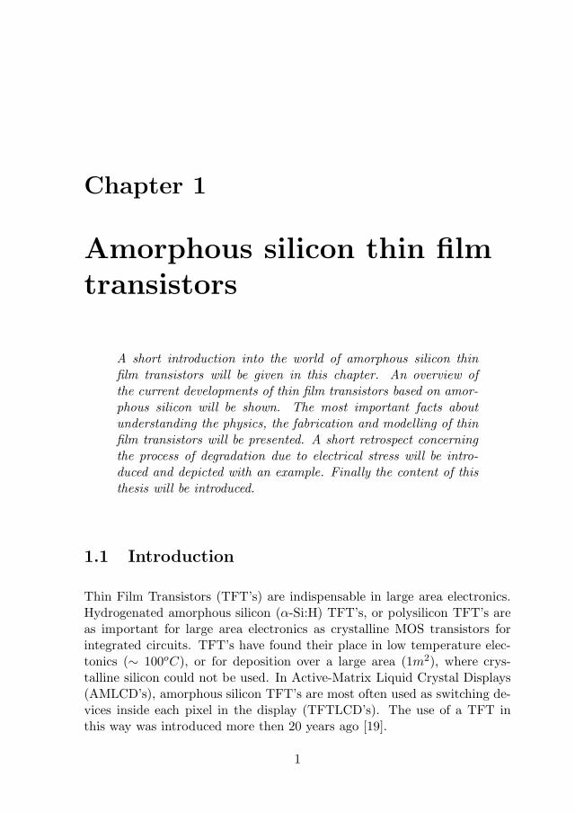
pens close to 70 V) the current is increasing with increasing voltage (∼ V 2),and after failing current starts to decrease with increasing voltage (TFTdamaged). Fig. 1.5 shows ID(VG) characteristics measured in 2 minuteslong break points. It can be observed that even before failing the transfercharacteristic of TFT shifted for ∼ 10V . The shift of the transfer char-acteristics represent actually an increase of threshold voltage. This largeshift of transfer characteristics is either due to the charge trapping or dueto creation of the states in the amorphous silicon layer.
1.2 Motivation
Although a lot of effort has been made to clarify the instabilities of electricalcharacteristics of thin film transistors, very little is known about their be-haviour under severe stress conditions such as electrostatic discharge stress(ESD). And on the other side, ESD failure is a hot topic in the displayindustry, as a large part of the damaged TFT displays originates from ESDfailure. The ESD problem is even more severe then in IC’s as the TFT’s arebuilt on the insulating substrate and often over the large area. Further, itis not possible to design an effective ESD protection using MOS transistorsswitched as bipolar transistors, the conventional solution for ESD protectionin IC’s.
Therefore the motivation for this work was the need for explanation of
8 Chapter 1. Amorphous silicon thin film transistors
-20 -10 0 10 20 30 40 50 60 70 80
V [V]G
0
0.2
0.4
0.6
0.8
1.0
1.2
I[
A]
D
before40V60V80V100V
Figure 1.5: Shift of transfer characteristics due to the electrical stress.
ESD failure in α-Si:H TFT’s. This knowledge is necessary required in thedesign of the transistors used in a ESD protection circuit. One of the firstgoals of this work was to identify failure under ESD stress and to modelthe failure. It was expected that α-Si:H TFT behave similarly to crystallineMOS transistors under ESD stress. It will be disproved in this thesis. It willbe clarified how a α-Si:H TFT respond to an ESD zap. The further challengeis to apply this knowledge for the purpose of design of ESD protection forTFT circuits.
1.3 Outline of the thesis
This thesis is focused towards testing and protection of hydrogenated amor-phous silicon thin film transistors for electrostatic discharge. The researchstarts with the experiments with ESD stress on single TFT’s. The resultsare further analysed and the ESD event in a single TFT is clarified. Thenan example of TFT circuit is manufactured and presented. Further ESDevent is investigated in TFT displays, by means of experiments and circuitsimulations. Finally the role of the ESD protection structures is discussed.The body of the thesis is organised as follows.
Chapter two gives the results of testing of grounded gate single TFT’son ESD stress. It describes the discharge event and how it can be mod-elled. Damage mechanisms and failures are dealt with. Dependence of thebreakdown voltage on technology parameters (channel length and width) is

1.3. Outline of the thesis 9
discussed. Also dependence of degradation and damage on stress duration.The results published in this chapter are based on the author’s publications[65], [66], [70], [47], [21], [68].
In chapter three electro-thermal simulations with a circuit simulator areused to identify the distribution and dissipation of temperature in α-Si:HTFT under ESD stress conditions. It is presented how the thermo-electricalnetwork is generated. A part of the results from this chapter are published,see [67].
In chapter four the influence of ESD stress on density of band gap statesin amorphous silicon is estimated. Density of states is calculated before andafter ESD stress and the impact of ESD stress is estimated. The resultsfrom this chapter are published in [69].
A practical example of an ESD problem in α-Si:H TFT circuit is pre-sented in chapter five. The application example, fingerprint sensor, is built.and furthermore it will be tested on ESD. Process flow and the results ofthe electrical and material characterisation is presented. The weakest pointof the sensor, ESD sensitivity, is analysed. The solution of the problem isdiscussed.
Finally chapter six gives an answer to the questions that we have oftenmet about how to design a TFT-based ESD protection structure. It isanalysed by means of electrical measurements and circuit simulations howa TFT display responds on ESD stress. Also the role of existing ESDprotection is tested and simulated. From the analysis of this ESD protectionstructures a number of recommendations for the design of ESD protectionin TFT circuits is drawn.
Chapter seven summarises the research and highlights the findings. Rec-ommendations for further research in the field of ESD stress on α-Si:H TFT’sare given.

10 Chapter 1. Amorphous silicon thin film transistors

Chapter 2
Electrostatic discharge stresson grounded gate α-Si:HTFT’s
A short introduction about electrostatic discharge stress will begiven in this chapter. The results of the ESD testing on amor-phous silicon TFT’s will be shown. The most important results ofthe testing with regard to the design parameters and the stress du-ration will be listed and analysed. The electrical model of degra-dation prior to electrical breakdown will be given. The results offailure analysis of the electrical breakdown will be shown.
2.1 Electrostatic discharge theory
Electrostatic discharge is a fast event of passing the triboelectric chargeaccumulated in an object (such as a human body or a transistor) to agrounded object. It happens in every day life all the time. People are everyday electrically charged and discharged. The process of discharge can bea small event, as the stinging sensation that you sometimes feel when youtouch the metal door handle, or it can be catastrophic event as it is the touchof a lightening. Something very similar happens with transistors. The onlydifference is that even a very low voltage, which a human body can takewithout any consequences, could damage or even destroy a transistor.
11

12 Chapter 2. Electrostatic discharge stress on grounded gate α-Si:H TFT’s
2.1.1 Electrostatic discharge models
When an electrostatic discharge failure is observed in an integrated cir-cuit, an analysis process aimed at identifying and solving the problem mustfollow. The basic failure mechanisms and electrical behaviour of a deviceinfluenced by ESD can be reproduced in a simpler form by using a briefvoltage pulse. Different experimental models are developed depending onthe way in which such brief voltage pulse originates. These ESD modelsare actually equivalent circuits or waveforms representing charging eventsexperienced by semiconductor devices. The most widely accepted model forthe use in industry quality and reliability testing is the Human Body Model(HBM). It represents human interaction with semiconductor devices thougha resistor R=1500 Ω and a capacitor C=100 pF. This model is defined bythe ESD Association Standard 5.1 [16]. Very similar is the Machine Model(MM). It represents contact of tools with semiconductor devices by a capac-itor C=200 pF. This model is defined by the ESD Association Standard 5.2[17].It is primarily used in Japan and in the automotive industry [10]. Thestress pulse in both model is modelled through the discharge of a chargedcapacitor. Furthermore, there is the Charged Device Model (CDM). Incontrast with the previous two models, the stress pulse is obtained throughdischarge of the charged semiconductor device itself via a pin. This modelis in the process of being defined. Currently there are two methods [10],one supporting the field-induced method [46] and the other supporting asocketed method ESD association standard D5.3 [18].
But unfortunately even the best models only approximate the reality.Apart of the approximate nature of the models, the ESD sensitivity of adevice (defined in volts and determined by using any of the defined models)in reality is additionally disturbed by the effect of parasitic inductors andstray capacitors. Therefore the test results are only a rough approximationto the ESD event. ESD sensitivity testing of devices, whether performedusing the CDM, MM or the HBM, is used to provide ESD sensitivity levelsfor the comparison of one device to another, as all these models providegood repeatability.
For a researcher working on a real ESD problem, only the data aboutESD sensitivity does not help to solve the problem. The real ESD event maybe dependent on the rise time of the ESD event, on its length, on device de-sign, fabrication technology, device package etc. The researcher needs moreinformation but only ESD sensitivity to establish the actual mechanism ofbreakdown, and in final to be able to prevent the ESD induced breakdown.A testing system that can provide some more information about the be-

2.1. Electrostatic discharge theory 13
haviour of a tested device under ESD stress is Transmission Line Model(TLM) system, where ESD stress is produced by a charged transmissionline, and which will be used for ESD experiments reported in this thesis. Itwill be explained in detail in Section 2.1.2.
2.1.2 Transmission Line Model testing system
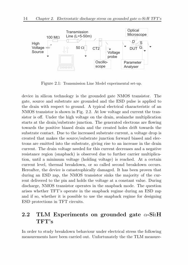
Transmission Line set-up was firstly introduced by Tim Maloney [36]. It wasinitially developed for ESD research, and it was proved to be a very impor-tant tool for the scientific approach to ESD problem, as it allows systematicstressing and also monitoring of device under stress during stressing. TheTLM system, was widely used for the studying of the transient behaviour ofelectrostatic discharge protection devices for the IC circuits as it is well cal-ibrated and easy to use. The parasitics can be kept small and repeatabilityis enhanced.
The TLM set-up is shown in Fig. 2.1. A 50 Ω coaxial cable (transmissionline) is first charged by the high voltage generator up to a known voltage.The amount of charge on the transmission line depends on its length. Whenthe line is discharged (the switch is closed) a short ESD pulse is created (10nanoseconds per meter of cable). The line is terminated with a 50 Ω resistorto minimise reflections. The voltage and the current can be monitored onthe oscilloscope, enabling accurate estimation of the power delivered in thedevice. A high-impedance transmission line model can be constructed byplacing a resistor (> 450Ω) in series with the device under test. This resistoris meant to provide that a voltage stress pulse is transformed into a currentstress pulse (as the serial resistance is much higher then the resistance ofthe device under test). The TLM is a step wise testing procedure. Thecurrent stress pulse is stepped up and the voltage on the device under testis measured.
2.1.3 On chip ESD protection strategy
To fully protect electrical circuits from the ESD, protection circuits areadded at every input, output and supply pin. The protection circuit has toprovide a conductive path to discharge the ESD stress. It has to limit thecurrent and the voltage in the circuit. It also has to stay invisible duringthe normal operation of the circuit.
This can be achieved using semiconductor devices such diodes and tran-sistors. The elements of the protection circuit must be designed to with-stand the high level currents and voltages. A very often used protection
14 Chapter 2. Electrostatic discharge stress on grounded gate α-Si:H TFT’s
Oscillo-scope
OpticalMicroscope
DUT
ParameterAnalyser
HighVoltageSource
D
G
S
100 M
50
TransmissionLine (L=5-50m)
CT2Voltageprobe
Figure 2.1: Transmission Line Model experimental set-up.
device in silicon technology is the grounded gate NMOS transistor. Thegate, source and substrate are grounded and the ESD pulse is applied tothe drain with respect to ground. A typical electrical characteristic of anNMOS transistor is shown in Fig. 2.2. At low voltage and current the tran-sistor is off. Under the high voltage on the drain, avalanche multiplicationstarts at the drain/substrate junction. The generated electrons are flowingtowards the positive biased drain and the created holes drift towards thesubstrate contact. Due to the increased substrate current, a voltage drop iscreated that makes the source/substrate junction forward biased and elec-trons are emitted into the substrate, giving rise to an increase in the draincurrent. The drain voltage needed for this current decreases and a negativeresistance region (snapback) is observed due to further carrier multiplica-tion, until a minimum voltage (holding voltage) is reached. At a certaincurrent level, thermal breakdown, or so called second breakdown occurs.Hereafter, the device is catastrophically damaged. It has been proven thatduring an ESD zap, the NMOS transistor sinks the majority of the cur-rent delivered to the pin and holds the voltage at a constant value. Duringdischarge, NMOS transistor operates in the snapback mode. The questionarises whether TFT’s operate in the snapback regime during an ESD zapand if so, whether it is possible to use the snapback regime for designingESD protections in TFT circuits.
2.2 TLM Experiments on grounded gate α-Si:H
TFT’s
In order to study breakdown behaviour under electrical stress the followingmeasurements have been carried out. Unfortunately the the TLM measure-

2.2. TLM Experiments on grounded gate α-Si:H TFT’s 15
Holding voltageVD
ID
Thermal breakdown
Snapback
Avalanche breakdown
Figure 2.2: IV characteristic of a NMOS emphasising the behaviour of the tran-sistor in the high current regime.
ments can not be performed in the way that is accepted in IC’s (it meansstressing by a current pulse). The on-resistance of α-Si:H TFT’s is muchhigher then of crystaline MOS transistors. The value of the on-resistancevaries, but it is in order of M Ω. As a consequence of this high on-resistancethe stress current is very low. Even the current under high ESD stress offew hundreds of Volts is so low that it can not be measured by the currenttransformer of the oscilloscope (sensitivity of which is 5 mA). Only the peakof the drain current can be measured. Also, the drain current during thebreakdown can be read out. That is shown in Fig. 2.3. It also should benoted that the gate and the source current during the breakdown are notknown, so the path of the breakdown current can not be established bythis measurement. The voltage data on the drain could be easily measuredby the oscilloscope. Therefore the standard TLM measurement system hadto be changed in order to compensate for the loss of data (current mea-surements) in the following way. Between each two TLM stress pulses, thetransfer characteristic ID(VG) of the TFT was monitored by the Parameteranalyser (Fig. 2.1). From the transfer characteristics important electri-cal parameters like threshold voltage, subthreshold slope were extracted.From the behaviour of the transfer characteristic the degradation flow wasestimated. Another important parameter that was measured by the Trans-mission Line model is the breakdown voltage. The measurement of the TLMvoltage showed that TFT’s give different response to the TLM stress thencrystalline MOS devices. The TLM voltage was increased up to the catas-
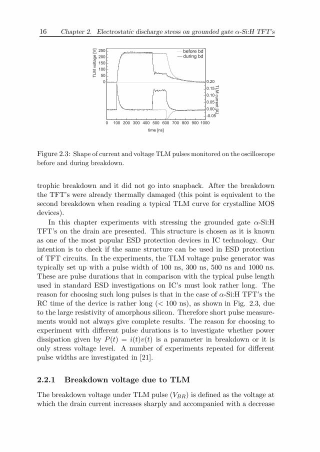
16 Chapter 2. Electrostatic discharge stress on grounded gate α-Si:H TFT’s
0 100 200 300 400 500 600 700 800 900 1000
0
50
100
150
200
250
TL
Mcu
rren
t[A
]
TL
Mvo
lta
ge
[V]
time [ns]
-0.05
0.00
0.05
0.10
0.15
0.20
before bdduring bd
Figure 2.3: Shape of current and voltage TLM pulses monitored on the oscilloscopebefore and during breakdown.
trophic breakdown and it did not go into snapback. After the breakdownthe TFT’s were already thermally damaged (this point is equivalent to thesecond breakdown when reading a typical TLM curve for crystalline MOSdevices).
In this chapter experiments with stressing the grounded gate α-Si:HTFT’s on the drain are presented. This structure is chosen as it is knownas one of the most popular ESD protection devices in IC technology. Ourintention is to check if the same structure can be used in ESD protectionof TFT circuits. In the experiments, the TLM voltage pulse generator wastypically set up with a pulse width of 100 ns, 300 ns, 500 ns and 1000 ns.These are pulse durations that in comparison with the typical pulse lengthused in standard ESD investigations on IC’s must look rather long. Thereason for choosing such long pulses is that in the case of α-Si:H TFT’s theRC time of the device is rather long (< 100 ns), as shown in Fig. 2.3, dueto the large resistivity of amorphous silicon. Therefore short pulse measure-ments would not always give complete results. The reason for choosing toexperiment with different pulse durations is to investigate whether powerdissipation given by P (t) = i(t)v(t) is a parameter in breakdown or it isonly stress voltage level. A number of experiments repeated for differentpulse widths are investigated in [21].
2.2.1 Breakdown voltage due to TLM
The breakdown voltage under TLM pulse (VBR) is defined as the voltage atwhich the drain current increases sharply and accompanied with a decrease

2.2. TLM Experiments on grounded gate α-Si:H TFT’s 17
in the drain voltage. In Fig. 2.4 some typical TLM curves are shownmeasured for TFT’s with different dimensions.
50 100 150 200 250 300 350 400 450 500
0.00
0.05
0.10
0.15
0.20
0.25
0.30
100/4
100/6
100/6
14/7
100/9
8/9
18/9
I TLM
[A]
VTLM
[V]
Figure 2.4: TLM curves shows different breakdown voltages for TFT’s with dif-ferent dimensions.
The results presented in this section are concerning two important sub-ject related to TLM stress induced breakdown:
• breakdown voltage vs. channel width and channel length
• breakdown voltage vs. pulse length.
An overview of the TFT’s with a variety of the channel length and widthtested by the TLM measurement system is given in Table 2.1. From thedata shown in Table 2.1 it can be quickly concluded that breakdown voltagedepends on the channel length and does not depend on the channel width(from the fact that the TFT’s with the constant channel length L = 9µmand with different channel widths did not show noticeable variations of thebreakdown voltage). The dependence of the breakdown voltage versus thechannel length , which is extracted from the data shown in Table 2.1, isseparately plotted in Fig. 2.5. Fig. 2.5 shows that breakdown voltagedepends almost linearly on the channel length for the short channel TFT’s(L < 10µm). For long channel TFT’s (L ≥ 10µm) the breakdown voltagestays constant with an approximate value of V br = 425V .
Beside the breakdown voltage measurements in the sample consisting ofthe TFT’s with W and L variations, an other experiment is carried out in or-der to get a better insight in the breakdown physics. The breakdown voltage

18 Chapter 2. Electrostatic discharge stress on grounded gate α-Si:H TFT’s
Table 2.1: Breakdown voltages under TLM stress in a sample with variations ofW and L.
W/L sample sample sample meanA1 B1 C1 value
100/10 420 450 410 427100/100 430 440 400 423
8/9 430 430 400 4204/9 430 430 400 42010/9 420 420 400 41318/9 410 410 400 4076/9 420 420 390 410
100/9 410 400 370 393100/8 370 370 320 35314/7 350 330 300 327100/6 280 280 260 27710/5 260 240 230 243100/4 210 190 190 197
was measured for different duration of the TLM stress pulse. Differencesin breakdown voltage due to difference in channel lengths/batches, maskpossible difference in breakdown voltages due to difference pulse lengths.Therefore for the following experiments only TFT’s were used with con-stant W/L ratio (18/9). In Table 2.2 the breakdown voltages of testedTFT’s are listed. These TFT’s were stressed with TLM pulses with pulselengths of 100 ns, 300 ns, 500 ns and 1 µs. It should be noted that the large(∼ 100ns) rise/fall time of the TFT has to be taken into account.
The data from Table 2.2 are graphically presented in Fig. 2.6. Theexperimental data show that the breakdown voltage lowers when the TLMstress time increases. Unfortunately the number of data points in the Fig.2.6 is not enough for a reliable extrapolation.
The conclusion that we can draw from the experiments is that the break-down voltage apparently depends on the channel length and does not on thechannel width. In the TFT’s with the channel length L < 10µm, so calledshort-channel effects, similar as in the standard crystalline devices, occursand the breakdown voltage is considerably lower. The current flow is de-pendant on the W/L ratio, but also on the channel length itself, due to

2.2. TLM Experiments on grounded gate α-Si:H TFT’s 19
190230270310350390430
4 5 6 7 8 9 10 100 L[µm]
V br[V ]
Figure 2.5: The mean value of the breakdown voltage versus the channel length.
punch through effect, which will be discussed later on. It is also shown thatthe breakdown voltage depends on the stress time. As the stress time isincreased, the breakdown voltage is decreased. These results suggests thatelectrical breakdown is in the end a thermal process. The heat generationis due to the current flow and it depends on the thermal properties of thematerials used, amorphous silicon, SixNy and glass. The time dependencesuggests also that a high power dissipation develops (Wunsch and Bell model[15]).
Table 2.2: Breakdown voltages of the TFT’s with W/L=18/9 tested by the TLMwith different pulse lengths.
100ns 300ns 500ns 1µssample T1 430 420 400 380sample T2 430 430 400 380sample T3 470 x 380 360sample T4 470 x 370 360sample T5 x x 380 360
mean value 450 425 386 368

20 Chapter 2. Electrostatic discharge stress on grounded gate α-Si:H TFT’s
360380400420440460
100 300 500 700 900 1100 t[ns]
V br[V ]
••
••
Figure 2.6: The mean value of the breakdown voltage versus the TLM stress time.
2.2.2 Pre-breakdown degradation due to TLM
If a TLM stress is higher than the ”threshold of degradation” (VTHDEG ∼180 V), the transfer characteristic, monitored between two TLM stresspulses, starts to change. The transfer characteristic shifts to the negativeside and the slope of the characteristic increases. A set of ID(VG) curvesmonitored in this way is shown in Fig. 2.7. The drain current behaviour un-
-4 -2 0 2 4 6 8 100
5
10
15
20W/L=10m/5m
TLM stress 0-280V, step=20V
I D
VG
[V]
[nA
]
Figure 2.7: Transfer characteristics monitored during the TLM series.
der applied gate voltage is already explained in Chapter 1, by equations 1.2,1.3 and 1.4. In literature, two mechanisms have been found to contribute todegradation effects in α-Si:H TFT’s:trapping of charge in the gate dielectric

2.2. TLM Experiments on grounded gate α-Si:H TFT’s 21
and change in the density of states (DOS) of the amorphous silicon itself.Which of this two set in during ESD stress will be investigated further inthis section. It is clear that change in the drain current might be due to
• the change in the threshold voltage, which can be due to the chargeaccumulation in the dielectric or at the interface dielectric/amorphoussilicon
• due to the change in the electron mobility. The electron mobility µn
is thermally activated with an energy given by the width of the tailstates, not by EC − EF [43].
µn = µ0NckT
ne−
EaT (2.1)
where µ0 is the extended state electron mobility, NC is the density ofstates at the mobility edge, n is the total electron density and Ea isthe activation energy which reflects the tail state distribution of the α-Si:H. Therefore the electron mobility might change if the temperatureof the TFT is changed.
The presence of the interface states can be read from the subthreshold slope.The sub-threshold slope is defined by:
S =dVG
d(logID)(2.2)
The change in the subthreshold slope will help us to distinguish whetherthe charges that are able to change threshold voltage are located in thegate dielectric (which produce no change in the subthreshold slope) or atthe gate dielectric/amorphous silicon interface which will produce changein the subthreshold slope).
The threshold voltage (VT ) is derived from the intersection of the slopeof linear characteristic with x-axis. It is found that once the TLM voltageexceeds the threshold of degradation, VT decreases linearly with appliedvoltage. The peak decrease in the threshold voltage is just before break-down. The breakdown voltage and TLM stress that a TFT can stand de-pends on the channel dimensions, as explained in 2.2.1. On the other hand,if the same amount of TLM stress is applied to TFT’s with different channeldimensions, the threshold voltage shift shows the same dependence with thechannel dimensions like the breakdown voltage. An overview of the VT shiftfor TLM stress of 500 ns and transistors with different channel dimensionsis shown in Fig. 2.8 [70]. Appearance of the negative shift of VT can be

22 Chapter 2. Electrostatic discharge stress on grounded gate α-Si:H TFT’s
Figure 2.8: Threshold voltage shift after TLM series (from 20 V up to 250 V) asfunction of W, L.
connected with both mechanisms, the creation of states in the amorphoussilicon layer, or near the interface and due to the charge trapping in the gatedielectric. For example, an amount of positive interface would cause an ac-cumulation of electrons in the channel, which would result in a lowering ofthe threshold voltage.
Besides VT , the transconductance is also derived from the slope of thelinear transfer characteristics. An increase of electron mobility is assumedand will be further explained by the analysis that follows. In α-Si TFT’s,the main carriers are electrons whose room-temperature mobility is typi-cally 0.3 − 0.6cm/V s. The dependence of the mobility with temperatureis given by equation 2.1. We suppose that a shift of VT and shift of µare independent processes, although they can be correlated, as shift in µwill almost certainly shift VT . We assume positive interface charges, whichwould help to move the current flow closer to interface α-Si/SiN and fur-ther from the bottom interface of α-Si/SiO2, where it is more confined inhigher mobility part of the band-gap. The fixed charge present in the gatedielectric causes bend bending at zero bias. Thus the DOS will be spatiallyinhomogeneous (in the direction of the channel depth) and determined bythe surface charge layer induced in the α-Si:H by the fixed charge in thegate insulator. There is also another possible mechanism which can helpto explain the change in the transfer characteristic’s slope, assuming thatinterface charges are inhomogeneous in the direction of the channel length.The assumption is that an amount of positive interface charges is createdclose to the drain. These positive charges would attract an accumulation

2.2. TLM Experiments on grounded gate α-Si:H TFT’s 23
layer (N+) that extends the drain, resulting in a shortening of the effectivelength of the transistor [73]. In this case electrom mobility stays constant.To avoid this uncertainty, the slope change will be presented through arelative change of transconductance:
gm =δIDδVG
=W
LµCVDS (2.3)
Stepped lowering of VT implies stepped accumulation of positive charges.Irreversibility of this degradation is observed and confirmed by means of re-peated TLM experiment under the same conditions. To investigate whetherthe SD induced degradation is permanent, repeated TLM stresses were ap-plied in the following way. In the first TLM series, TLM stress (VTLM ) isstepped from 20 V up to 250 V, when the series is stopped. After 100 minof pause (with all electrodes grounded) the second TLM series is repeated(VTLM =20-250 V). This time both VT and gm stay constant during TLMstress. After pause of 1000 min the third TLM series is applied (VTLM wasincreased from 20 V up to dielectric breakdown). Same as in the previ-ous case, no degradation is found for voltages up to 250 V. Finally, whenVTLM >250 V, then degradation of VT and gm continues with the same rate(1 V/100 V) as in the first TLM series (Fig. 2.9).
0 50 100 150 200 250 3004.0
4.5
5.0
5.5
6.0
VT
[V]
VTLM[V]
0 50 100 150 200 250 300
1.0
1.1
1.2
1.3
g/g
mm
0
V [V]TLM
Figure 2.9: Threshold voltage and transconductance behaviour during the firstand the repeated TLM series.
It should be noted that after the first TLM stress the ”turnaround phe-nomenon” of the threshold voltage shift is noticed. This phenomena for thelow negative gate bias is already known in the literature [62] and it appearswhen the negative threshold voltage shift caused by the hole trapping in theSiN gate dielectric are positively compensated by the states created near theconduction band in the α-Si film. This process of state creation should bedistinguished from the creation of states under high electric field.

24 Chapter 2. Electrostatic discharge stress on grounded gate α-Si:H TFT’s
In order to distinguish whether these charges are located in the gatedielectric or at the gate dielectric/amorphous silicon interface, the sub-threshold slope of the transfer characteristics is analysed. It appears thatsub-threshold slope increases during TLM stressing, which can be the re-sult of interface state creation. Assuming that created defects in amorphoussilicon are located at the gate dielectric/amorphous silicon interface, the ef-fective defect density Dit can be related to the sub-threshold slope [9] as:
S = ln10kT
q
(1 +
q2Dit
Ci
)(2.4)
where q is the electron charge, k is the Boltzmann constant, Ci is gatecapacitance per unit area and T is absolute temperature. The calculatedvalues of the density of interface states vary between TFT’s. For example,after a TLM series up to 250 V they are estimated to be in the order of1012cm−2eV −1. The behaviour of the subthreshold slope under TLM stressis shown in Fig. 2.10.
6 8 10 12 141E-11
1E-10
1E-9
W/L=14m/7m
VTLM
= 40-260V, step 10V
I D[A
]
VG
[V]
Figure 2.10: Subthreshold slope change during TLM.
2.2.3 Where are the defects?
The sub-threshold slope increase during TLM stressing implies defect statecreation. In order to determine where these defect states are located withinvolume of a TFT a repeated symmetrical experiment is performed as fol-lows. After the first TLM series (VTLM=50-250 V, step=10 V) is applied onthe source of the TFT, the second TLM series is applied on TFT’s drain.In the second TLM series the VT decrease and gm increase continuously

2.2. TLM Experiments on grounded gate α-Si:H TFT’s 25
from the same threshold of degradation voltage, when compared to the firstseries (Fig. 2.11). Apparently, repetitive TLM stresses on one side of thetransistor up to the highest previous level do not create additional damage,whereas an additional TLM series with the same low voltage on the otherterminal does create additional damage. It means that if TLM stress isapplied on the drain, the defect states are non-equally distributed along thechannel. They are located close to the drain of TFT.
100 150 200 250
5
6
7
8
VT
[ V]
VTLM
4
3
2
50 50 100 150 200 2500.9
1.0
1.1
1.2
1.3
1.4
1.5 TLM on source
TLM on drain
VTLM
g/g
mm
0
Figure 2.11: Threshold voltage and transconductance variation under two re-peated symmetrical TLM series (first series on the source, second on the drain).
2.2.4 CV measurements showing interface states creation
An additional proof that TLM stress induces creation of fast interface statesis obtained from high frequency C(V) measurements [23]. Parasitic capac-itances of the drain and the source are measured before and after a TLMseries up to 200V applied on drain. The position of the Fermi level in anundoped α-Si, as used in this investigation, is shifted closer to the bottomof the conduction band. Therefore, tested TFT’s are undoped and n-type(Fig. 2.1cv). It should be noted that during the TLM testing the TFT’sthreshold voltage is decreased by 0.5 V, and the transconductance is slightlyincreased. As it is shown in Fig. 2.12, the high frequency C(V ) curves ofthe parasitic capacitance of the source before and after TLM stress are thesame, meaning that TLM stress did not induce any damage at the sourceside. In contrast, the high frequency C(V ) curve of the parasitic capaci-tance at the drain side (Fig. 2.12) after TLM stress is stretched-out to thenegative side and degraded as compared with the curve monitored beforethe TLM stress.

26 Chapter 2. Electrostatic discharge stress on grounded gate α-Si:H TFT’s
-30 -20 -10 0 10 20 300.6
0.7
0.8
0.9
1.0before
afterr TLM
CG
D/C
SiN
voltage [V]
-30 -20 -10 0 10 20 30
0.7
0.8
0.9
1.0before
after TLM
CG
S/C
SiN
voltage [V]
Figure 2.12: Normalised high frequency capacitance vs voltage curves measuredfor the gate/source overlapping and gate/drain overlapping capacitances before andafter TLM stress applied on the drain.
2.2.5 Modelling of TLM stress induced degradation
Firstly, the gradually distributed electric field across the gate dielectric issimulated using Silvaco device simulator [14] for the TFT in gg mode. Thesimulation shows that if the threshold voltage of degradation is applied onthe drain, the electric field close to drain has value ∼ 5− 10 MV/cm. Thiselectric field peak is located close to the drain, but it expands from drain tosource during each next TLM stress pulse, since the TLM stress is stepped.
The assumption that a TLM stress creates positive interface charges,giving rise to sub-threshold slope and lowering VT , is interpreted by meansof electrical simulations. The assumed model says that the new createdinterface charge, induced by the electric field, widens with every step alongthe interface from the drain to the source (Fig. 2.13). The transfer charac-teristic of the top gate amorphous silicon transistor is simulated by Silvaco

2.2. TLM Experiments on grounded gate α-Si:H TFT’s 27
simulation tools [14], taking into account created interface charge. Initially,the transfer characteristic is simulated without any interface charge. Ateach simulation step a constant quantum of interface charge is added alongthe length from drain to source (Fig. 2.13). Charge parameters have beenoptimised, leading to: length of the cube x = 0.2µm and fixed charge den-sity quantum of 1012cm−2. The result of the simulations is presented inFig. 2.14. It can be seen that it describes the experimentally measuredcharacteristics, shown in Fig. 2.7. This is the effect of the positive inter-
semiconductor
-Si:H
n+ -Si:H
gate dielectricSiNxHy
glass
lightshield
q1q2q3q4q5q6S D
Gate
Figure 2.13: Model of stepped accumulation of the interface charges from q1 untilq6.
I[A
]D
4E-7
3E-7
2E-7
2E-7
0.00 2 4 6 8 10 12 14 16 18 20
W/L=100 m/6 m
V [V]G
x=0.1 m-2.7 m, step=0.2 m
Figure 2.14: Simulated transfer characteristics with increasing interface charge asdepicted in Fig. 2.13.
28 Chapter 2. Electrostatic discharge stress on grounded gate α-Si:H TFT’s
face charges, which help creating an inversion layer ”extending” the drain.If we assume negative charges in the channel (α-Si:H), the effect will be thesame. Negative states in the band gap of amorphous silicon are the statesin the upper part of the band gap, donor-like states. Conduction band-tailstates are neutral when empty and negative when filled [12].
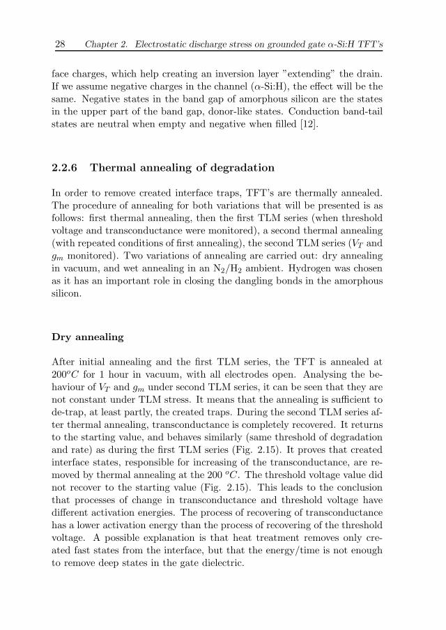
2.2.6 Thermal annealing of degradation
In order to remove created interface traps, TFT’s are thermally annealed.The procedure of annealing for both variations that will be presented is asfollows: first thermal annealing, then the first TLM series (when thresholdvoltage and transconductance were monitored), a second thermal annealing(with repeated conditions of first annealing), the second TLM series (VT andgm monitored). Two variations of annealing are carried out: dry annealingin vacuum, and wet annealing in an N2/H2 ambient. Hydrogen was chosenas it has an important role in closing the dangling bonds in the amorphoussilicon.
Dry annealing
After initial annealing and the first TLM series, the TFT is annealed at200oC for 1 hour in vacuum, with all electrodes open. Analysing the be-haviour of VT and gm under second TLM series, it can be seen that they arenot constant under TLM stress. It means that the annealing is sufficient tode-trap, at least partly, the created traps. During the second TLM series af-ter thermal annealing, transconductance is completely recovered. It returnsto the starting value, and behaves similarly (same threshold of degradationand rate) as during the first TLM series (Fig. 2.15). It proves that createdinterface states, responsible for increasing of the transconductance, are re-moved by thermal annealing at the 200 oC. The threshold voltage value didnot recover to the starting value (Fig. 2.15). This leads to the conclusionthat processes of change in transconductance and threshold voltage havedifferent activation energies. The process of recovering of transconductancehas a lower activation energy than the process of recovering of the thresholdvoltage. A possible explanation is that heat treatment removes only cre-ated fast states from the interface, but that the energy/time is not enoughto remove deep states in the gate dielectric.

2.3. Long time experiments 29
0 2 4 6 8 10 124.0
4.5
5.0
5.5
6.0
6.5
7.0
1. TLM
TLM after annealing
VT
[V]
Number of TLM stress pulses
0 2 4 6 8 10 120.96
1.00
1.04
1.09
1.13
gm
/gm
0
1. TLM
TLM after annealing
Number of TLM stress pulses
Figure 2.15: Effects of dry thermal annealing on threshold voltage and transcon-ductance.
Wet annealing
A completely different result is obtained by wet open-circuit thermal an-nealing in the atmosphere of N2 with the presence of H2 at 250 oC for30 min. The results are shown in Fig. 2.16. As shown in Fig. 2.16, thethreshold voltage after thermal annealing is increased (in contrast to thedry annealing), while transconductance is almost completely recovered, al-though it does not return exactly to the starting value. Both VT and gmunder the second TLM series are active (changing with increasing the TLMstress), they degrade in the same way as under the first TLM series, whichimplies that created states are removed from the α-Si:H/SiN interface. Thedifference in VT shift during wet and dry annealing comes from the presenceof hydrogen. Annealing without the presence of hydrogen gives negative,while annealing in the presence of hydrogen gives positive shift, as hydrogenplays important role in the process of de-trapping holes.
2.3 Long time experiments
A square voltage pulse in the range of seconds is applied to the drain ofa TFT using a parameter analyser HP4142B and a voltage generator ex-pander. The stress pulses are increased in voltage up to 200 V, the highestvoltage that can be generated by the parameter analyser equipped with avoltage expander. During each stress pulse the drain current is measuredand after each stress pulse the transfer characteristics are measured, bothwith the same parameter analyser.

30 Chapter 2. Electrostatic discharge stress on grounded gate α-Si:H TFT’s
0 2 4 6 8 10 12 14 16 18 20 224.00
4.50
5.00
5.50
6.00
6.50
7.00V
T[V
]
1. TLM
TLM after annealing
Number of TLM stress pulses
0 2 4 6 8 10 12 14 16 18 20 22
0.95
1.00
1.05
1.10
1.15
gm
/gm
0
1. TLM
TLM after annealing
Number of TLM stress pulses
Figure 2.16: Effects of wet thermal annealing on threshold voltage and transcon-ductance.
2.3.1 Current during stress
Both, the voltage and the current during stressing were measured. As thevoltage during stress is given by the voltage generator, the voltage is con-stant. The information of the current during stress is important, bearingin mind that that information was lost during TLM measurements. Thecurrent during stress measured on both the drain and the source of theTFT with W/L = 18/9 is shown in Fig. 2.17 for stress voltage on the drainVD=200 V, with the source and the gate grounded. It can be concludedfrom the plot that the current during stress is drain to source current, astwo curves shown in Fig. 2.17 overlap, except for the first point. It shouldbe noted that the drain current during stress is in the beginning (low drainvoltages) only a subthreshold (leakage) current, as the gate is grounded.Expected level of the leakage current is in the order of several pico amps.After the drain stress voltage is increased, the real conduction current (or-der of µA) sets in. Due to the high voltage applied on the drain, the DIBLeffect is initiated, as it will be explained further in section 2.5.
Another important remark about the drain current during stress is thatalthough the drain current level measured with each stepped voltage stressincreases, during a stress pulse the current shows an exponential decay (Fig.2.17). This decay is due to the process of creation/removal states acrossthe amorphous silicon layer. This process is confirmed from the measuredtransfer characteristic after stress, as it will be explained later in this section.The current during stressing reflects the creation/removal of states at theinterface, but also in the bulk of α-Si (reaching final steady state situationin this process takes some time - if it is reached at all [47]?).

2.3. Long time experiments 31
0.0 0.2 0.4 0.6 0.8 1.0
0.06
0.08
0.10
0.12
0.14
0.16ID
IS
Str
ess
cu
rre
nt
[A
]time [s]
Figure 2.17: Current during Long pulse stress measured on the drain and thesource (the source current is actually measured with the negative sign, plotted aspositive for convenience.
2.3.2 Breakdown voltage due to Long pulse
Due to the limitations of the measurement set-up (stress voltage only up to200 V), the breakdown voltage under long pulse stress could be measuredonly for the TFT’s that have a breakdown voltage lower than 200 V. There-fore the breakdown voltage measurements were limited on the short channelTFT’s. Two TFT’s were measured: W/L = 100/6 and W/L = 100/4. Forthese TFT’s the breakdown voltages of 150 V and 110 V are measured,respectively, under the stepped stress of 1 s. Also TFT with W/L = 18/9was tested, but it did not breakdown up to 200 V stress of 1s. The currentmeasured on the drain one step before and during the breakdown is shownin Fig. 2.18.
0.0 0.2 0.4 0.6 0.8 1.0
1E-10
1E-9
1E-8
1E-7
1E-6
1E-5
1E-4
VD=140V
VD=150V
I D[A
]
time [s]
Figure 2.18: Pre-breakdown and breakdown current during Long pulse stress.

32 Chapter 2. Electrostatic discharge stress on grounded gate α-Si:H TFT’s
2.3.3 Pre-breakdown degradation due to Long pulse
Pre-breakdown degradation is monitored in the same way as it was under theTLM stress. From the measured transfer characteristics, values of thresholdvoltage, subthreshold slope and transconductance are extracted. All theseparameters show the similar behaviour as under the TLM stress.
Threshold voltage , sub-threshold slope and transconductance showssimilar behaviour as under TLM stress. Therefore the experimental re-sults will not be discussed in details, but only in general. An overview ofthe pre-breakdown degradation measured on the TFT with W/L = 18/9under Long pulse stress of different lengths is given in Table 2.3. There
Table 2.3: Pre-breakdown degradation of the TFT’s with W/L=18/9 tested bythe Long pulse with different pulse lengths.
Stress [V] 0÷ 50 50÷ 125 125 ÷ 200VT /0 gm 0 S 0/ 0/
are three distinguished regions in the behaviour of monitored parameters.While stress voltage is low (VD <50 V) there is a slight increase in the VTfollowed with also very small decrease of S. This is initial change that isknown in the literature and it is called the turnaround phenomena and it wasalready mentioned in section 2.2.2. After the stress voltage is increased fur-ther (50< VD <125 V), an other region could be recognised when thresholdvoltage decreases moderately (∆VT < 1 V), the transconductance increasesand the subthreshold slope stays same as in the previous region. In thisregion there is no significant creation/removal of interface states and theprocess of charge trapping in the gate dielectric dominates. After the stressvoltage is higher then 125 V, VT degrades severely (∆VT ∼ 3V ), while gmdecreases severely and S increases sharply. In this region creation/removalof interface states in the amorphous silicon layer dominates in the processof degradation.
2.4 Time-voltage trade-off
In this section the time-voltage trade-off is presented in order to give anin-depth analysis of the ESD effects in α-Si:H TFT’s. The data presented

2.4. Time-voltage trade-off 33
in this section are actually drawn from the experimental results shown pre-viously in section 2.2 and section 2.3.
2.4.1 Breakdown voltage over time
The question we want to have an answer to is whether the breakdown de-pends on the stress time or it is only related to the stress level. That isimportant information to determine the mechanism of breakdown. The de-pendence of the power of the square pulse and the time to failure is due tothe energy consumed at TFT, as explained by the Wunsch and Bell model[74], [15]:
E =∫ t
0I(t)V (t)dt (2.5)
It is an early model of thermal breakdown in Si devices. In this modelthe pulse power and time to failure are related by P ∼ t1/2. This modelcovers only the middle part (typically for Si that is in the region 10 ns< t <100µs) of the P (t) curve. For very short failure time (t < 10ns), the littleheat is developed so that the process is adiabatic P ∼ t−1. For very largefailure times, typically above 100µs and after thermal equilibrium has beenestablished, the constant or steady state term dominates.
Unfortunately, there are not enough (accurate) breakdown voltages mea-sured for different pulse lengths using TFT’s with the same W/L. The datameasured under TLM stress are shown in Fig. 2.6, and the same TFT(W/L = 18/9) could not be measured by Long pulse stress. Only the smallnumber of data for TFT’s W/L = 100/6 and W/L = 100/4 are available.In these two TFT’s the breakdown voltage change from 240V under TLMstress to 150V under Long pulse stress and from 180V to 110V , respectively.Still, from this limited data source it is possible to draw the conclusion thatbreakdown voltage depends on the pulse duration, e.g. it lowers if the pulselength of applied stepped voltage stress increases, but a unique function ofthis dependence is not known. Though the current in TFT under squarevoltage pulse proves not to be constant in time (it exponentially decreaseswith time), we could assume from equation 2.5 that VBR lowers if the pulselength of applied stepped voltage stress increases. This conclusion impliesthat the breakdown due to ESD stress in TFT’s is a thermal breakdown.The power-density-dependant failure of amorphous silicon TFT was pre-viously investigated in [61] in the range 1-10 ms. From the power of thesquare stress, knowing the volume of the melted area, the melting point ofthe breakdown can be calculated. That will be mentioned later in section2.6.
34 Chapter 2. Electrostatic discharge stress on grounded gate α-Si:H TFT’s
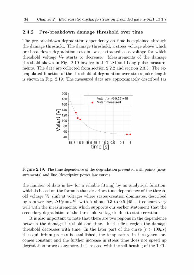
2.4.2 Pre-breakdown damage threshold over time
The pre-breakdown degradation dependency on time is explained throughthe damage threshold. The damage threshold, a stress voltage above whichpre-breakdown degradation sets in, was extracted as a voltage for whichthreshold voltage VT starts to decrease. Measurements of the damagethreshold shown in Fig. 2.19 involve both TLM and Long pulse measure-ments. The data are collected from section 2.2.2 and section 2.3.3. The ex-trapolated function of the threshold of degradation over stress pulse lengthis shown in Fig. 2.19. The measured data are approximately described (as
1E-7 1E-6 1E-5 1E-4 1E-3 0.01 0.1 1
40
60
80
100
120
140
160
180
200
Vsta
rt[V
]
time [s]
Vstart(t)=t^(-0.29)+49Vstart measured
Figure 2.19: The time dependence of the degradation presented with points (mea-surements) and line (descriptive power law curve).
the number of data is low for a reliable fitting) by an analytical function,which is based on the formula that describes time dependence of the thresh-old voltage VT shift at voltages where states creation dominates, describedby a power law, ∆VT = atβ, with β about 0.3 to 0.5 [45]. It concurs verywell with the measurements, which supports our earlier statement that thesecondary degradation of the threshold voltage is due to state creation.
It is also important to note that there are two regions in the dependencebetween the damage threshold and time. In the first region the damagethreshold decreases with time. In the later part of the curve (t > 100µs)the equilibrium process is established, the temperature in the system be-comes constant and the further increase in stress time does not speed updegradation process anymore. It is related with the self-heating of the TFT,

2.5. Device simulations 35
as the states creation is a thermal process. Self-heating will be analysed inthe Chapter 3.
2.5 Device simulations
2.5.1 Theoretical introduction
The breakdown of amorphous silicon devices was earlier investigated indiodes [5], or in an antifuse structure [1], where an evidence was found ofimpact ionisation in a-Si. In the thin film transistors itself a huge amount ofwork and research was focused on metastable effects in amorphous silicon,but very little was published on the subject on electrical breakdown. Theitems that have to be clarified about electrical breakdown in α-Si:H TFT’sare:
• is there punch-through?
• is there impact ionisation and avalanche breakdown?
• is there snapback?
Before the results of simulations regarding these questions will be shown, afew basic definitions will be introduced. The punch-through effect occurswhen the neutral substrate width is reduced to zero at a sufficient drainvoltage and the source depletion region is in direct contact with the draindepletion region. At this point, the source is effectively short circuited tothe drain, and a large current can flow. What actually happens is thatunder high drain bias the channel depletion width is no longer constantalong the length of the device, but varies from the source to the drain. Thiseffect is called Drain Induced Barrier Lowering (DIBL) Effect and it occurswhen higher drain voltage is applied to the device. It is very well known inMOS devices [3]. The surface potential (band bending) along the channelbetween source and drain for long channel devices is normally constant. Inshort devices, or in long devices under very high drain biasing, it happensthat the peak of the surface potential is reduced and is constant only overa small part of the channel, if at all. Since the peak surface potential isreduced, which means that the barrier is lowered, the current will increase.
Avalanche multiplication that may occur by means of impact ionisationis very well explained in standard crystalline Si devices [11]. Electrons/holesgain so much energy in a high electric field that they can generate extraelectron-hole pairs by exciting electrons from the valence band into the con-duction band. In this way an avalanche of free carriers may arise. Could we

36 Chapter 2. Electrostatic discharge stress on grounded gate α-Si:H TFT’s
expect an avalanche multiplication due to impact ionisation in amorphoussilicon in our TFT’s?
It has been already confirmed by the experimental results shown inthis chapter that the snapback regime in TFT’s is not detectable by ESDtesting such as TLM. This stands in opposition with the expectations, asthe snapback regime is known in all similar crystalline silicon devices, likeNMOS transistors and even n-well resistors [37]. If impact ionisation at thedrain/bulk junction due to the high electric field is proved to be present,then the holes concentration inside the n α-Si bulk starts to rise signifi-cantly. Then the source/bulk junction should become forward biased andthe electrons from the source n+ region would contribute to the drain cur-rent. This process is self-enhancing, as a lower external voltage is neededto maintain impact ionisation. This is seen as a snapback. An interestingissue is to verify the concentration of electrons and holes across the channellength of a TFT under ESD conditions.
2.5.2 Simulation results
The electrical simulations of TFT’s are performed by Silvaco process anddesign simulation software [14]. The effect of DIBL is shown through thesimulations of:
• surface potential of an a-Si:H TFT under high drain bias
• surface potential of a long- and a short-channel TFT under the samebiasing conditions.
In Fig. 2.20 is shown how the surface potential is distributed along thechannel for three different drain biases (VD=10, 20, 50 V). In all casesthe gate voltage was kept constant. It should be noted that the simulatedTFT was scaled in lateral direction, which means that channel length andthe drain biasing are divided with the factor 10. So the channel length ofsimulated device was L = 0.6µm, under drain bias (VD=1, 2, 5 V). That isdone for the simplicity. It slightly influences the accuracy of the simulationresults, but does not influence the conclusion extracted from the results atall. This figure shows that by increasing the drain bias, we decrease thebarrier. It proves that the DIBL effect is present in α-Si:H TFT devices.It also helps us to understand the results obtained from the experiments.In the experiments the drain was stressed. The gate was grounded, so thatthe device was not active in the conductive mode. Initially, under verylow drain voltage a low leakage current was flowing through the channel.

2.5. Device simulations 37
As the drain voltage was increased, the DIBL effect was more and morepronounced. When the drain voltage is large enough, the real current flowsthrough the device.
Pote
ntial[V
]
Pote
ntial[V
]
Pote
ntial[V
]
Pote
ntial[V
]
Vd=1VVd=2VVd=5V
0.1 0.2 0.3 0.4 0.5 0.1 0.2 0.3 0.4 0.5
0.1 0.2 0.3 0.4 0.5 0.1 0.2 0.3 0.4 0.50
0
Figure 2.20: An example of DIBL effect in amorphous thin-film transistors simu-lated for various drain voltages (VD=10, 20, 50 V).
In another example it is shown that the same effect of barrier loweringcan happen if the channel length is varied. Therefore a TFT with twodifferent channel lengths is simulated. The results of these simulations ispresented in Fig. 2.21. The simulations show that with shortening of thechannel, the barrier between source and drain is lowered. It also agreeswith our experimental observations. Namely, it was noticed that both thethreshold of degradation and the breakdown voltage depend on the channellength. The shorter TFT’s degrade and fail earlier than the longer ones.
The previous simulation results prove the presence of the punch-throughin α-Si:H TFT’s. It shows that the punch-though occurs when drain voltageis high enough to suppress the barrier in surface potential between sourceand drain. It happens earlier in shorter devices from the reason that in theshort channel devices the barrier is already initially lowered. What we wantto know further is if the depletion width at drain extends far enough in realdevice to have punch-through.

38 Chapter 2. Electrostatic discharge stress on grounded gate α-Si:H TFT’s
Figure 2.21: Surface potential distribution for TFT’s along the channel obtainedfor examples with different channel lengths.
The question of the impact ionisation and the avalanche breakdown isanalysed through the simulation of the recombination/generation rate understepped drain bias. The results of the simulations performed for a constantgate voltage (VG=25 V) and different drain biasing are shown in Fig. 2.22.Fig. 2.22 shows (please note that the drain voltage and the channel lengthare scaled with factor 10) that the peak generation rate is located at thedrain, in case when stress is applied to the drain. The generation peakvalue in the TFT with the channel length L = 0.6µm changes from G =9·1010 1
scm3 for VD=1 V to G = 1·1021 1scm3 for VD=10 V and G = 3·1025 1
scm3
for VD=20 V. As the results are scaled by factor 10, it allows us to comparethis result with the TFT with L = 6µm and VD=10, 100, 200 V, althoughwe must be aware that linear scaling of both voltage and size is not the sameas scaling the problem, as depletion layer width goes with V 1/2...1/3. Theexperiment shows that the breakdown in the TFT with L = 6µm occurringat 280 V could really be initiated by avalanche breakdown at the drain side.In this case we can expect an generation rate G > 3 ·1025 1
scm3 . This level ofgeneration is enough to start an avalanche breakdown. Simulation resultsprove that an avalanche breakdown is possible in amorphous silicon TFT’sunder ESD stress conditions provided similar physical models for ionisationcan be used for crystalline and amorphous silicon.
Finally the presence of snapback is examined. A short (L=0.6 µm)ggTFT is stressed by 40 V on the drain. This situation is similar to 400

2.5. Device simulations 39
Distance along the channel [ m]
Ge
ne
ratio
nra
te[s
cm
]-1
-3
Depth[ m]0
0.40.8
1.21.6
0-1e+10-2e+10-3e+10-4e+10-5e+10-6e+10-7e+10-8e+10-9e+10
gate
00.1
0.20.3
0.40.5 0
0.40.8
1.21.6
0
-5e+12
-1e+13
-1.5e+13
-2e+13
-2.5e+13
-3e+13
Vd=10V
gate
00.1
0.20.3
0.40.5 0
0.40.8
1.21.6
0
-2e+20
-4e+20
-6e+20
-8e+20
-1e+21
gate
00.1
0.20.3
0.40.5 0
0.40.8
1.21.6
0
-5e+24
-1e+25
-1.5e+25
-2e+25
-2.5e+25
-3e+25
Figure 2.22: Generation rate simulated under constant gate VG=25 V and varyingdrain biasing VD=1, 5, 10, 20 V.
V stress on a TFT with L=6 µm. Simulated structure, recombination andconcentration of holes and electrons are shown in Fig. 2.23. The peak ofelectric field is situated at the drain/bulk junction. This is where the impactionisation sets in. The generation rate of G = 9·1028 1
scm3 is simulated at thesame location. The holes and electrons flows away from this location towardsthe source and the drain contact, respectively. The amount of holes in thebulk/ back channel region is increased several orders of magnitude, still itseffect is not strong enough to seriously contribute to the output current. Itcan therefore be concluded that the snapback effect in amorphous silicon isdisturbed due to the properties of amorphous silicon.

40 Chapter 2. Electrostatic discharge stress on grounded gate α-Si:H TFT’s
Figure 2.23: Simulated TFT with potential distribution within the α-Si layer, sim-ulated concentration of holes and electrons through the bulk and the recombinationthrough the bulk.
2.6 Post-breakdown observation
Finally, post-breakdown observations have been carried out using opticalmicroscopy and scanning electron microscopy (SEM). The observation con-firms the location of the breakdown spot close to the drain in case whenthe ESD stress is applied to the drain. This further support our conclusionthat avalanche creates onset of breakdown in short devices. In long-channeldevices, where breakdown voltage is higher then in the short-channel de-vices, electric field close to drain at the moment of breakdown is very highand very close to the value of the critical electric field for silicon nitride (thevalue 5-6 MV/cm is found in the literature for the stoichiometric Si3N4. Thesilicon nitride used in TFT’s is not stoichiometric and the breakdown fieldvalue may vary. Electrical field propagation during a stepped TLM stressis simulated. TLM voltage was applied on the drain (ggTFT). Distributionof the electric field is shown in Fig. 2.24 for the drain voltage VD=200 V.In this case the peak field (close to the drain) is 7.5 MV/cm. Simulated

2.6. Post-breakdown observation 41
TFT has a burried metal layer that shields the amorphous silicon from thebacklight. Increasing the TLM stress up to 350 V the field peak is increasedup to 10 MV/cm. This could indicate that not only avalanche is cause ofbreakdown, but under sufficiently high drain voltage that is also the fieldacross the dielectric. Actually, the most often found failure mode is the
Figure 2.24: Electrical field in the ggTFT with the lightshield under TLM stress(200 V) on the drain.
gate dielectric breakdown . It appears as a rupture localised close to thedrain, with a center at the edge between drain and channel. Exceptionsare short channel devices, where the rupture completely covers the channellength. In this case, because of the punch-trough, the avalanche generationrate is no longer confined to the drain side. The size of the rupture indicatesthat the breakdown is a high temperature event. The temperature of thebreakdown was calculated on basis of the rupture size, assuming a sphericalvolume of the whole rupture, and the temperature of over 1400oC is esti-mated. The assumption of the spherical volume is made after the ruptureswere examined under the microscope. The location of the rupture indicatesthe position of the highest temperature peak. After inspection of failed de-vices the assumption is made that the highest peak of the temperature islocated at the edge between the drain and the channel, as it is shown in Fig.2.25. Fig. 2.25 shows example of gate dielectric breakdown in a TFT withL = 6µm, after etching of the top gate electrode. The size of the breakdownspot is large so that it covers almost the whole channel length. The centreof the breakdown spot is located exactly on the drain/gate edge.
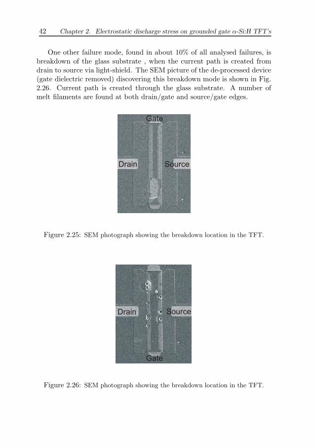
42 Chapter 2. Electrostatic discharge stress on grounded gate α-Si:H TFT’s
One other failure mode, found in about 10% of all analysed failures, isbreakdown of the glass substrate , when the current path is created fromdrain to source via light-shield. The SEM picture of the de-processed device(gate dielectric removed) discovering this breakdown mode is shown in Fig.2.26. Current path is created through the glass substrate. A number ofmelt filaments are found at both drain/gate and source/gate edges.
Drain Source
Gate
Figure 2.25: SEM photograph showing the breakdown location in the TFT.
Drain Source
Gate
Figure 2.26: SEM photograph showing the breakdown location in the TFT.

2.7. Summary 43
2.7 Summary
Experiments were performed on a single grounded gate (gg)TFT to deter-mine TLM failure threshold, in terms of voltage-to-failure profile as thepower-to-threshold can not be measured by the TLM system (the TLMcurrent of a single ggTFT is too low). The performance was measuredfor various values of the channel length and width. A linear relation thebreakdown voltage/channel length has been measured. The experimentsshowed that a degradation of the threshold voltage appears during TLMstress prior to the breakdown. Device level electrical simulations were doneto explain the observed degradation mechanisms. The pre-degradation hasbeen related to the created charges localised close to the stressed electrode.
The experiments were continued by using a prolonged ESD stress on aggTFT, in order to find out the time-voltage relation.
Further, device level electrical simulations have been performed to findout the presence of punch-through and avalanche multiplication. The sim-ulations revealed the presence of the DIBL effect in TFT’s, which is morepronounced in the short-channeled TFT’s.
Optical failure analysis showed the dielectric breakdown in two modes.The breakdown location is determined; in the long channel devices at thedrain, while in the short-channel TFT’s it is across the whole channel length.

44 Chapter 2. Electrostatic discharge stress on grounded gate α-Si:H TFT’s

Chapter 3
Thermal analysis under ESDconditions
This chapter presents the results of a study of the self-heatingeffects in amorphous silicon thin film transistors. The methodof electro-thermal coupled simulations will be explained. Theresults of two and three-dimensional simulations will be given.The results of the simulations in the static mode will be shownas well as in the transient mode.
3.1 Introduction
Although industrial interest in TFT’s in the last years is increased as displayindustry is developing, this is the first attempt in studying the self-heatingeffect in amorphous silicon TFT’s. Our interest in thermal modelling ofTFT’s came from our previous experimental study presented in Chapter 2,when a systematical study of electrostatic discharge effects has been done.The devices investigated were top-gate amorphous silicon TFT’s with va-riety of design parameters (channel length and width). Please note that anumber of devices is protected by a light-shield (like in Fig. 2.24). Dielectricbreakdown, appearing in two variations, is determined by failure analysis.The most often failure mechanism is located in the gate dielectric. In casethat breakdown is thermally activated, than it can be assumed that longchannel TFT’s have lower temperature peak under same biasing, i.e. bet-ter temperature dissipation (lower gradient of the temperature across thechannel). The applied stress induces, before catastrophic breakdown oc-curs, degradation of electrical parameters (such as lowering of the threshold
45

46 Chapter 3. Thermal analysis under ESD conditions
voltage and increasing of the electron mobility), but this degradation is notthe direct or only cause of the catastrophic breakdown, as the degradationlevel is different in different TFT’s at the moment of breakdown. The short-channel devices break down early, although their electrical parameters arevery little degraded at that point. In other words, different processes leadto dielectric breakdown and degradation. Although it is possible that bothof the processes are thermally activated. In analysing sub-threshold slopemeasured between stress pulses, it is found that creation of positive inter-face states is responsible for degradation. This result is also validated bymeans of Silvaco-Atlas device simulations. With the assumption that elec-trical breakdown is thermally initiated, it becomes interesting to simulatethe location of the highest temperature within a TFT. This work on thermalmodelling of TFT’s uses an approach of two- and three-dimensional circuitsimulations. This approach allows that variations of temperature, currentand voltages within the transistors active area are calculated.
3.2 Non-isothermal device simulation
This method for simulation of self-heating effects uses an electrical circuitwhere currents represent heat flow and voltages represent temperatures.The power dissipation of a transistor in the electrical circuit is modelledwith a current source in the thermal circuit. Current in the thermal cir-cuit represents the heat dissipation across the device. The principle of thismethod is shown in Fig. 3.1. The thermal resistance and thermal capaci-
Electrical circuit Thermal circuit
TFT
rv i=P
VG VD Tamb C
rl
Figure 3.1: Principle of the thermal-electrical circuit simulation method.

3.2. Non-isothermal device simulation 47
tance of the amorphous silicon are modelled in the thermal circuit with anelectrical resistor and an electrical capacitor respectively. The thermal cir-cuit is coupled with the electrical circuit by means of the temperature andpower dissipation. The voltage at thermal circuit is equivalent of temper-ature in electrical circuit. The temperature in electrical circuit is involvedby change in carrier mobility. The carrier mobility change is approximatedby equation [43]:
µ = µ0e−Ea
kT (3.1)
where activation energy Ea=0.1 eV, Boltzmann constant k = 8.6 · 10−5, Tis absolute temperature and µ0 is chosen so that carrier mobility at 300K isµ = 0.3 cm2/Vs [13]. The circuit simulator Pstar [40] is used to determinesteady state and transient solutions of these coupled circuits. The circuitscan be solved in two ways: simultaneously (coupled) and sequentially (un-coupled), as circuit simulator Pstar allows control of electrical mobility byelectrical variables. In simultaneous simulations all voltages and tempera-tures are solved in the same time. In the sequential simulations the electricalcircuit is solved first, than the results are used as input parameters for thethermal circuit. The result of thermal simulations is again used as input(temperature) for electrical circuit etc. In this work simultaneous approachis used. Sequential approach is used only during programming process toverify obtained results. The problem with non-isothermal device simula-tions is that the thermal and the electrical geometric domain are different.The thermally active area is much larger. In three-dimensional simulationsit can produce very large number of elements and a long execution time.Often compromise must be made between accuracy of the simulation andcomputer time, although in this simple TFT’s structure should not be alimitation.
3.2.1 TFT modelling using Pstar
Before electrothermal simulations have been performed, it is first checked ifa TFT can be simulated with Pstar. The model used in these simulations isPstar MOS model, level 301, which allows change of transistor’s parameters,such as mobility and threshold voltage. To compare simulated character-istics with measured ones, parameters are set at µ = 0.3cm2/Vs, VT=2V, L = 100µm and W = 1000µm. The simulated characteristic, shownin Fig. 3.2, shows that level of the output drain current is similar to themeasured current. It was also checked if carrier mobility behaves accordingto given equation. It should also be noted that switching characteristics of

48 Chapter 3. Thermal analysis under ESD conditions
crystalline MOS transistors are much better than once of the TFT’s, butit is assumed that it would not influence the quality of the simulations, sothis model has been accepted.
1.00E-11
1.00E-10
1.00E-09
1.00E-08
1.00E-07
1.00E-06
1.00E-05
1.00E-04
0 5 10 15 20
Vg [V]
Id[A
]
Figure 3.2: Transfer characteristic of TFT simulated by Pstar MOS model.
3.2.2 Electrothermal model
In electro-thermal simulations, current and voltage distributions over a TFTactive area are calculated. In that order, the TFT is split up into a number ofsections. Depending on the mesh, 2D and 3D simulations are distinguished.In 2D simulations, a TFT is split into number of sections along the TFT’slength. In 2D simulations all these sections have the same width, which isequal to the width of TFT itself. In 3D simulations each of these sectionsis split into number of sections along the TFT’s width, allowing calculationof the temperature distribution in both directions of channel length andchannel width of the TFT.
In the first stage two-dimensional simulations are performed. Geomet-rical representation of the simulated structure is shown in Fig. 3.3. Theelectrically active area of the TFT is split into ten sections (by dashed linesA-K in Fig. 3.3), each with its own current, voltage and temperature. Thethermal circuit is created within a thermally active area, which is inevitablylarger then the electrically active area, with its own mesh that only coin-cides with the mesh for electrical circuit in the areas where heat is generated.The electrical circuit of the model is shown in Fig. 3.4. For the electrical

3.2. Non-isothermal device simulation 49
SOURCE DRAIN
GATE
A B C D E F G H I J K
Figure 3.3: Geometrical representation of top gate TFT.
network, a TFT with dimensions W = 20µm and L = 10µm is modelledwith a serial connection of ten TFT’s with W = 20µm and L = 1µm.
VDVG
Figure 3.4: 2D electrical model of a TFT.
Before electrothermal simulations started, this concept of modelling of aTFT with serial connection of TFT’s had been verified. The same exampleused in Fig. 3.2 is simulated to compare previous results of simulationsof a TFT with the simulation of this model. As shown in Fig. 3.5 (leftaxis) the simulated output drain current is the same as the current shownin Fig. 3.2. In addition to this model verification, in the same plot it isalso shown how the lateral effects are automatically incorporated using thismodel. Thanks to the fact that voltage on each of TFT’s is not equal,current naturally must be equal in the serial connection, then the powerdissipation and consequently the temperature are not equally distributedbetween TFT’s in the serial connection. Distribution of voltages at each of

50 Chapter 3. Thermal analysis under ESD conditions
ten TFT’s in serial connection (right axis) is shown in Fig. 3.5. Biasingconditions are VD=10 V, VG=0-20 V. At the first moment, all drain voltagestays on the last TFT in the row, as the last TFT is at the drain side.As soon as it starts to conduct, the other TFT’s start too. After all ofTFT’s are in the saturation region (VG >15 V), voltage among them is stillnon-equally distributed.
1.0E-12
1.0E-11
1.0E-10
1.0E-09
1.0E-08
1.0E-07
1.0E-06
1.0E-05
1.0E-04
1 3 5 7 9 11 13 15 17 19 21
Vg [V]
Id[A
]
0
1
2
3
4
5
6
7
8
9
10
Vtf
t[V
]
Figure 3.5: Current and voltage distribution among 10 TFT’s in serial connection.
As the electrical circuit is verified as satisfying, the thermal circuit is tobe built. Although the mesh that is used in this simulation is extremely sim-ple, as it is made manually, the thermal circuit is already more complicated.It comes from the reason that the active area for thermal circuit is largerthan the active area for the electrical circuit, as temperature is dissipatedinto the glass substrate. In this case, only two extra layers surrounding theelectrically active area are taken into account. The scheme of the thermalcircuit is given in Fig. 3.6. The part of the circuit that is circled representone section in the electrically active area of TFT. Thermal resistances arecoloured in different shades of gray in order to distinguish their differentmeanings. Resistances at the top central part represent thermal behaviourin electrically active area (white). They are surrounded by a number of lat-eral resistances that represent the junction between amorphous Si and glass(dark gray). The rest of the circuit belongs to the glass area (light gray).It should be noted that temperature is taken into account only in the bot-tom part of the device (amorphous silicon layer and under it) and thermal

3.2. Non-isothermal device simulation 51
dissipation through nitride and metal connections has been neglected.
Tamb
Figure 3.6: Thermal circuit used in 2D simulations.
For each of the circuit elements used in the thermal network a model hasto be defined with spatial dimensions as parameters. The dependence of athermal resistance and capacitance on the spatial co-ordinates is determinedby the heat flow equation:
CTδT
δt= H + κ∆T (3.2)
where C is the thermal capacitance per unit of volume in JK−1cm−3, Tis the temperature in K, H is the heat generation per unit of volume inWcm−3, κ is the thermal conductance in WK−1cm−1. If we introduce ananalogy between the thermal capacitance per unit of volume with electri-cal capacitance per unit of volume, the thermal conductivity with electricalconductivity, the temperature with voltage and the heat generation withelectrical current, than heat equation is analog to the following partial dif-ferential equation:
CδV
δt= i+R∇V (3.3)
For solving this differential equation system must be discrete. In a three-dimensional discrete system current flow is allowed in direction of x, y and z

52 Chapter 3. Thermal analysis under ESD conditions
axis. To solve the equation the boundary conditions must be given. Bound-ary conditions are determined by means of ambient temperature and inputpower dissipation. Finally, we can represent the temperature distribution ina network of electrical resistances and capacitances. An elementary volumeis represented in Fig. 3.7. As current through the capacitance is C = δV
δt , it
HEAT FLOW
l W
d S
Figure 3.7: Definition of elementary dimensions in a section.
follows that all thermal capacitances must be connected to the ground. Ascurrent through resistance is i = R∆V then resistances are connected intoa network. For the three-dimensional rectangular mesh, the solution for thethermal resistance is:
RTH =l
κS(3.4)
where l and S are dimensions shown in Fig. 3.7. The heat capacitance isgiven by:
CTH = Cp · S · d (3.5)
where Cp is specific heat per volume in JK−1cm−3. The thermal resis-tance at the junction of two materials is calculated direction as a parallelconnection of two thermal resistors:
RTH = RTH1‖RTF2 (3.6)
A mesh is generated using the simplest concept of classical rectangular mesh-ing. A rectangular domain is divided into smaller rectangles by a classicalmesh. Dimensions used in building of the thermal mesh are up to free choiceof the researcher. His choice is of course limited with the computer speed.Physical quantities are calculated within the volume of mesh cubes. Onepossible choice of mesh dimensions used in this simulation is given in Fig.3.8. The top layer thickness is set at 360nm which is in reality representing
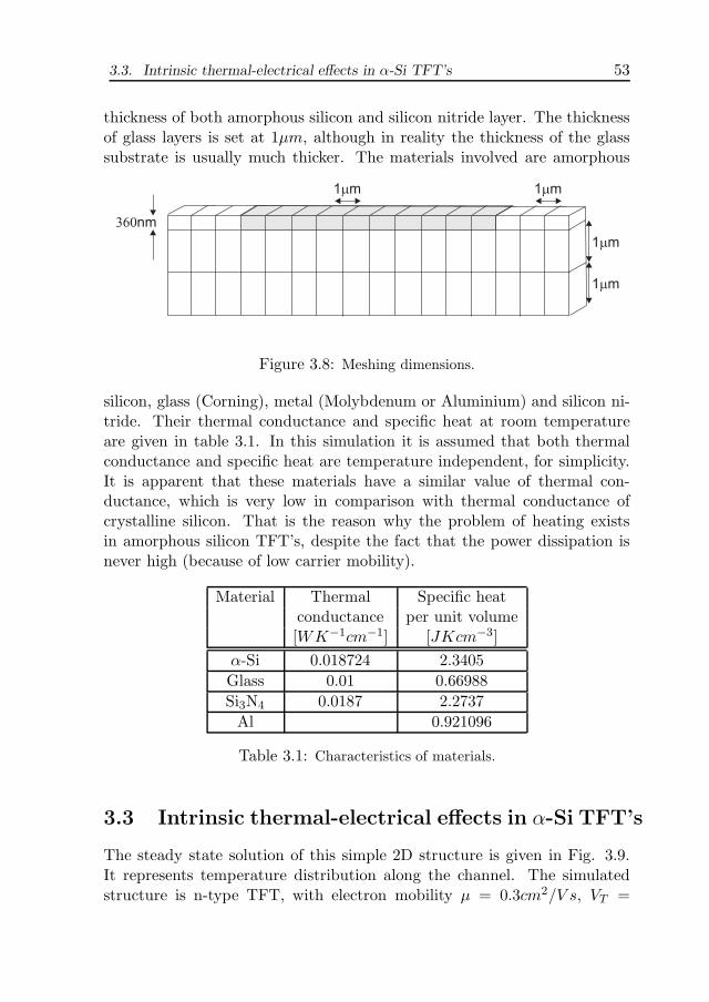
3.3. Intrinsic thermal-electrical effects in α-Si TFT’s 53
thickness of both amorphous silicon and silicon nitride layer. The thicknessof glass layers is set at 1µm, although in reality the thickness of the glasssubstrate is usually much thicker. The materials involved are amorphous
1 m 1 m
1 m
1 m
nm
Figure 3.8: Meshing dimensions.
silicon, glass (Corning), metal (Molybdenum or Aluminium) and silicon ni-tride. Their thermal conductance and specific heat at room temperatureare given in table 3.1. In this simulation it is assumed that both thermalconductance and specific heat are temperature independent, for simplicity.It is apparent that these materials have a similar value of thermal con-ductance, which is very low in comparison with thermal conductance ofcrystalline silicon. That is the reason why the problem of heating existsin amorphous silicon TFT’s, despite the fact that the power dissipation isnever high (because of low carrier mobility).
Material Thermal Specific heatconductance per unit volume[WK−1cm−1] [JKcm−3]
α-Si 0.018724 2.3405Glass 0.01 0.66988Si3N4 0.0187 2.2737Al 0.921096
Table 3.1: Characteristics of materials.
3.3 Intrinsic thermal-electrical effects in α-Si TFT’s
The steady state solution of this simple 2D structure is given in Fig. 3.9.It represents temperature distribution along the channel. The simulatedstructure is n-type TFT, with electron mobility µ = 0.3cm2/V s, VT =

54 Chapter 3. Thermal analysis under ESD conditions
6V and bias conditions are VD = 350V and VG = 50V . As voltage isapplied on drain and the source is grounded, the temperature has the highestpeak at the drain side. Moving closer to the source side, the temperaturedecays. The temperature at the source side has value that is very close toroom temperature. Extension of 2D simulation to 3D simulation is obtained
0
50
100
150
200
250
300
350
400
T [oC]
TFT 20/10
Figure 3.9: Steady state solution for 2D simulation.
by splitting the TFT in the channel width direction. The scheme of theelectrical circuit used in 3D simulations is shown in Fig. 3.10. The totalchannel width is split in 5 rows, which do not interact in the electrical,but only in the thermal circuit. It is possible that electrical current existsin the lateral direction. Simulation of this current would be possible if aTFT would be added between two neighbour nodes in two consequent rows.In this case this lateral current is neglected for simplicity. In our case, aTFT with dimensions L = 10µm, W = 100µm is modelled with a networkof 50 TFT’s with dimensions L = 1µm and W = 20µm. For building ofthe thermal circuit for 3D simulation, the same method is applied as in2D simulations. The only difference is that part of the circuit is added torepresent temperature dissipation into direction of new added dimensions.The new part of the circuit has the same mesh used for lateral dissipation in2D dimensions. The results of 3D simulations obtained under steady stateconditions are presented in Fig. 3.11. Transistor dimensions are L = 10µmand W = 100µm. The transistor model is n-type TFT. Biasing conditionsfor both simulations are: VD = 350V , VG = 50V .

3.3. Intrinsic thermal-electrical effects in α-Si TFT’s 55
VD
VG
Figure 3.10: Electrical circuit as used in 3D simulation.
3.3.1 Transient simulations for different ESD pulse duration
The result of a transient analysis is given in Fig. 3.12. Firstly, an ESD eventis simulated, with voltage pulse of length 100ns, with rise and fall time of10 ns, applied on the drain. Gate voltage is VG = 50V , source is grounded.In this time scale self-heating process is not completed, In other words, thetemperature has still not come to the value calculated in DC simulation (atthe hottest point 325 oC). Length of applied drain pulse is increased insteps (100 ns, 200 ns, 500 ns, 1 µs, 100 µs and 1 s) in order to determinewhen self-heating process is completed. For drain pulse lengths of 100 ns,200 ns, 500 ns and 1 µs the hottest point temperature is increasing withtime and yet is not reached equilibrium. Also, there is not much differencebetween temperature between rows. The temperature is homogeneouslydistributed over device. For pulse length of 100 µs, the temperature comesto saturation and the level of temperature is the same as the previous onefrom DC analysis. It saturates after 15 µs (Fig. 3.12). Finally, for thelength longer than that, as it is shown in Fig. 3.12 for pulse length of 1 s,the temperature is constant.
Thermal simulations of TFT’s include many approximations, which arenot present in reality, so it would be difficult to give a reliable answer tothe question what is the temperature level under certain current and volt-ages. Nevertheless, the distribution of temperature is determined. It canbe described as:
• if a voltage is applied on the drain, than the drain becomes the hotregion.

56 Chapter 3. Thermal analysis under ESD conditions
0
50
100
150
200
250
300
350
T [oC]
TFT 100/10
Figure 3.11: Steady state 3D simulation.
• if the same voltage is applied on the drain, then steady state conditionswill produce much higher temperatures than transient in a time rangeof a couple hundreds nanoseconds.
The most important value of this simulation is that the simulated distri-bution of temperature corresponds to the results shown in the Chapter 2.The question that was not answered in the Chapter 2 is whether the changeof breakdown with the change of the stress time is related to the thermalheating. The transient simulations of the self-heating are the link we needto completely unveil the process of ESD failure in TFT’s. A relation be-tween Fig. 3.13 and section 2.4.1, where it was shown how the breakdownvoltage depends on the stress duration. If we relate the experimental factswith the results of the transient simulations, we can state that after theTFT enters thermal equilibrium and constant temperature is established,the breakdown voltage will become constant.
It was mention earlier in section 2.4.2 that there are two distinguishedregions of the damage creation over time. There is a region when the damagethreshold decreases with time (t < 100µs and a region when the damagethreshold stays constant although stress time is increased, as shown in Fig.2.19. That behaviour was extracted from the experimental results and it canbe explained with the help of the Fig. 3.13. Namely, the damage creation isa thermal process. Therefore the amount of the created states depends on

3.3. Intrinsic thermal-electrical effects in α-Si TFT’s 57
the temperature of the system. Therefore the threshold of damage creationdepends on the stress time due to the fact that the temperature in thesystem depends on the stress time as well. For very short stress times(t < 100µs) the temperature of the system changes with time (Fig. 3.13).After 100 µs the temperature of the system is constant with increasing thestress time, which means that if the stress time is longer than that, theprocess of damage creation starts always with the same voltage.
3.3.2 Self-heating in TFT’s with different channel length
Electro-thermal simulations of the TFT’s with variations of the channellength have been performed in order to show the temperature distributionover the TFT area in the short and long TFT’s. The biasing conditionsare: gate voltage VG=60 V and drain voltage VD=100 V. These biasingconditions are chosen to show the heat generation in the most severe case.The simulations were performed under assumption that the heat generationis equally distributed in all four lateral directions over glass area.
The area surrounding the devices was the same in all simulations. Onlythe channel length was varied, while the channel width was constant, as wellas the drain and the source metal contacts widths. The simulated structureis designed according to the top-gate device built on a glass substrate andfrom the top side passivated over all device area, used in the experimentalprocedure. The temperature distribution shown in Fig. 3.14 is the temper-ature of the glass substrate in the first layer under the amorphous siliconlayer. In Fig. 3.14 the channel length area has on the x-axis a finer grid thanthe surrounding substrate. The temperature distribution over TFT’s shownin Fig. 3.14 is similar in all four cases. The simulations show that the tem-perature peak is located always at the drain side. Across the channel length,the temperature decreases from drain to source. In case of short devices thedistribution is very much uniform across the channel length. For the chan-nel length of L = 4µm (Fig. 3.14 ), the simulation shows that the TFT isoverheated. The simulated temperature is impossibly high (∆T = 2400oC),so it implies that in the reality the TFT would be already broken down.Fig. 3.14 shows that in the TFT with L = 6µm the temperature is rela-tively high (∆T = 120oC). The device with L = 10µm suffers much lowerheating (∆T = 28oC). Finally, the device with the length 100µm is notheated (∆T < 1oC). The simulations confirm that short channel devicessuffer from more pronounced thermal heating due to the larger localisedpower dissipation.

58 Chapter 3. Thermal analysis under ESD conditions
3.4 Summary and future work
Electro-thermal coupled simulations have been performed to find out if aTFT under the ESD stress suffers from self-heating. The simulation methoduses an electrical circuit coupled with a thermal circuit. The thermal circuitis an electrical circuit where currents represent heat flow and voltages rep-resent temperatures, a current source represents the power dissipation. Thesimulation method has been explained, 2D simulations have been performedin DC and 3D simulation have been preformed in DC and transient regime.A number of simulations has been preformed for TFT’s with different chan-nel length and for different ESD pulse durations. It was concluded that thetemperature peak in a grounded gate TFT stresses on the drain is locatedat the drain side of the α-Si:H channel. As expected, our simulation resultsindicated that the self-heating is much more pronounced in short-channelTFT’s. Simulation results also reveal that the time-constant of a TFT is15 µs, prolonging the stress after 15 µs will not increase the self-heating.The simulations prove that, upon specifying a critical temperature at whichfailure is declared, the breakdown voltage of a TFT under ESD conditionschanges with the channel length/temperature and the temperature/ESDduration relation.
As TFT’s are very simple devices from the point of view of their geo-metrical design, they are rather easy to simulate. For given examples, theexecution time of transient 3D simulation is about 30 seconds. It is dueto the fact that only rectangular mesh is used, but also due to very simplesimulated structure. It is possible to refine this work by:
• using a better mesh (by Lumex or any similar program as mesh gen-erator)
• using design structure which would be more similar to the real struc-ture (including metal lines for drain, source, gate and light-shieldwhich would act as a heat sink in the thermal circuit)
• taking into account the feedback effect of the local device temperatureon the thermal conductivity and specific heat
• simulating TFT’s with different channel length, and check if exper-imentally obtained result that higher breakdown voltage (i.e. lowertemperature peak) corresponds to longer channel length
• thinking about a TFT structure that overcomes the self-heating prob-lem and increases the breakdown capability of TFT’s and that can be

3.4. Summary and future work 59
used in the ESD protection structures (this issue is reported in section3.3)
• changing pulse length in the transient simulations with different pulselength, rise and fall time. Also it could be possible to determine whenthe temperature will reach saturation, i.e. time constant of heatingup the system.

60 Chapter 3. Thermal analysis under ESD conditions
TFT 100/10
0
50
100
150
200
250
300
350
400
1 11 21 31 41 51 61 71 81 91 101
time [ns]
Vd
[V]
0
20
40
60
80
100
120
T[o
C]
drain voltage
drain at 1. row
drain at 2. row
drain at middle row
drain at 4. row
drain at 5. row
TFT 100/10
0
50
100
150
200
250
300
350
400
1 11 21 31 41 51 61 71 81 91 101
time [2ns]
Vd
[V]
0
20
40
60
80
100
120
140
T[o
C]
drain voltage
1 row, D
2. Row, D
Middle row, D
4. Row, D
5. Row, D
TFT 100/10
0
50
100
150
200
250
300
350
400
1 11 21 31 41 51 61 71 81 91 101
time [5ns]
Vd
[V]
0
20
40
60
80
100
120
140
160
180
T[o
C]
Vd
1. Row, D
2. Row, D
middle row, D
4. Row, D
5. Row, D
TFT 100/10
0
50
100
150
200
250
300
350
400
1 11 21 31 41 51 61 71 81 91 101
time [10ns]
Vd
[V]
0
50
100
150
200
250
T[o
C]
Vd
1. Row, D
2. Row, D
Middle row, D
4. Row, D
5. Row, D
TFT 100/10
0
50
100
150
200
250
300
350
400
1 11 21 31 41 51 61 71 81 91 101
time [us]
Vd
[V]
0
50
100
150
200
250
300
350
400
T[o
C]
Vd
1. Row, D
2. Row, D
Middle row, D
4. Row, D
5. Row, D
TFT 100/10
0
50
100
150
200
250
300
350
400
1 11 21 31 41 51 61 71 81 91 101
time [100ms]
Vd
[V]
0
50
100
150
200
250
300
350
400
T[o
C]
Vd
1. Row, D
2. Row, D
Middle row, D
4. Row, D
5. Row, D
Figure 3.12: Transient 3D simulation calculated at the five points at the drainside for different pulse duration a.) stress time 100 ns, Tmax= 100 oC, b.) stresstime 200 ns, Tmax= 120 oC, c.) stress time 500 ns, Tmax= 160 oC, d.) stress time1 µs, Tmax= 200 oC, e.) stress time 100 µs, Tmax= 330 oC and f.) stress time 1s, Tmax= 330 oC.
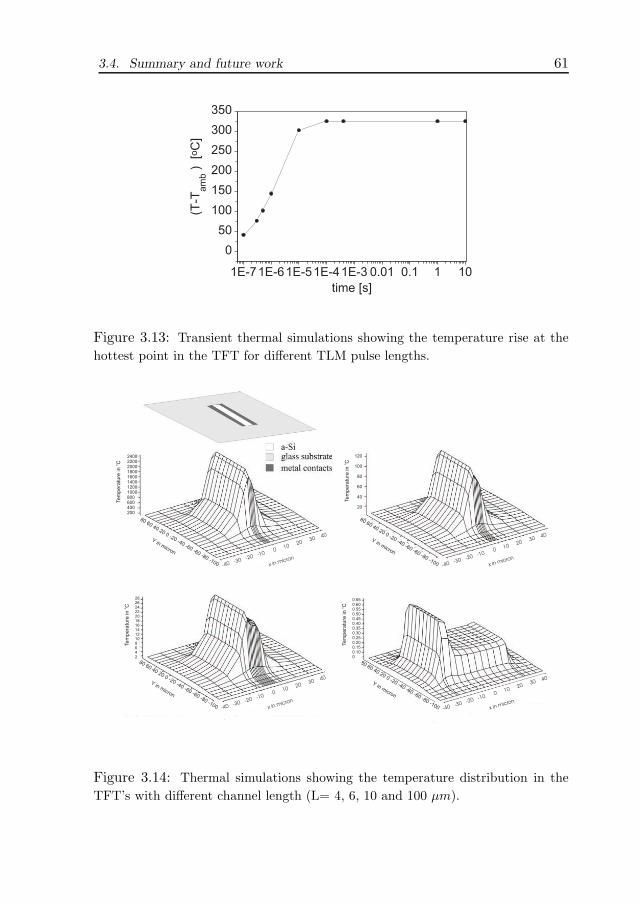
3.4. Summary and future work 61
1E-71E-61E-51E-41E-3 0.01 0.1 1 10
0
50
100
150
200
250
300
350
(T-T
am
b)
[oC
]
time [s]
Figure 3.13: Transient thermal simulations showing the temperature rise at thehottest point in the TFT for different TLM pulse lengths.
-40-30
-20-10
010
2030
40
x in micron
80 60 40 20 0 -20 -40 -60 -60 -80 -100
Yin micron
24002200200018001600140012001000800600400200
Tem
pera
ture
inC
o
-40-30
-20-10
010
2030
40
x in micron
80 60 40 20 0 -20 -40 -60 -60 -80 -100
Yin micron
Tem
pera
ture
inC
o
120
100
80
60
40
20
-40-30
-20-10
010
2030
40
x in micron
80 60 40 20 0 -20 -40 -60 -60 -80 -100
Yin micron
Tem
pera
ture
inC
o
282624222018161412108642
-40-30
-20-10
010
2030
40
x in micron
80 60 40 20 0 -20 -40 -60 -60 -80 -100
Yin micron
Tem
pera
ture
inC
o
0.650.600.550.500.450.400.350.300.250.200.150.100
Figure 3.14: Thermal simulations showing the temperature distribution in theTFT’s with different channel length (L= 4, 6, 10 and 100 µm).

62 Chapter 3. Thermal analysis under ESD conditions

Chapter 4
Band-gap density of statesunder ESD stress
In this chapter intrinsic properties of the amorphous silicon layerin a TFT under ESD stress conditions will be analysed. Thedensity of states within band gap induced by ESD stress will beinvestigated. A method for calculation of the density of stateswill be presented and then used to calculated the density of statesbefore and after applying ESD stress.
4.1 Theory of band-gap density of states
The atomic network of amorphous silicon is disordered and can have allrange of silicon bonds, such as covalent bonds, week bonds, dangling bondsand due to the presence of hydrogen also silicon-hydrogen bonds. There arecertain energies in the band gap which corresponds to the specific siliconbonds. Not more then two electrons with different spin could have the sameenergy level, therefore the energies of the bonds are spread all over the bandgap. These bonds still obey a certain distribution. In the first place, bondswithin the band gap could be divided into tail states and deep states. Tailstates are located next to the edges of the conductance and valence bands.They appear due to the silicon week bonds. Deep states are located as thename says deep into the band gap. They are due to the dangling bonds.States close to the conductance band are equivalent to donor states. Theyare be charged positively. The closer to the conductance band, the morepositive charge they have. States close to the valence band are equivalentto acceptor states. They can be negatively charged. Therefore states in the
63

64 Chapter 4. Band-gap density of states under ESD stress
N(E)
E
D- D
0 D+
ECEV
Figure 4.1: Energy gap states in amorphous silicon.
middle of the band gap are neutral. The distribution of the tail states isrepresented by a linear function and the distribution of the deep states bya sum of Gaussian functions, as it is shown in Fig. 4.1. The energy gapEc − Ev is typically around 1.8 eV at room temperature. In hydrogenatedamorphous silicon the majority of defects are passivated with hydrogen,reducing the density of the deep states to typically 1016 cm−3.
There are different models developed to describe numerically densityof states. The method for determing the density of states function N(E)throughout most of the energy gap, which will be used in this thesis, isbased on field-effect conductivity measurements.
4.2 Field-effect method for DOS estimation
An analytical method, which correlates the density of states within the en-ergy band gap and field-effect conductivity measurements, was firstly pro-posed in the seventies [35]. Shortly, from the measured ID(VG) character-istic, the amount of space charge induced by voltage VG can be calculated.Since then, the method is further enhanced by many authors [24], [50],[12], [27], [20]. Powell [42] gave an overview of different variations of thismethod, and a discussion of the approximations introduced in them, suchas constant space-charge density and zero-temperature statistics. It wasshown that from field-effect conductance measurements only the broad fea-tures of the density of states can be determined and a unique N(E) is notidentifiable. Later on [30], it was shown by Fortunato et al. that a class ofmethods called approximate methods of directly extracting the DOS [24],
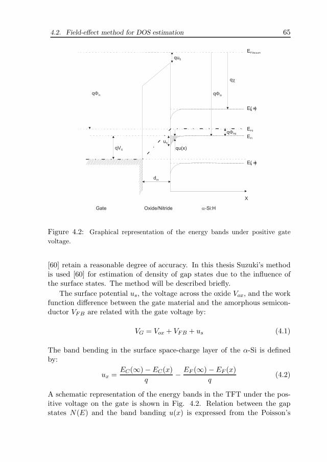
4.2. Field-effect method for DOS estimation 65
X
Gate Oxide/Nitride -Si:H
E( )C
E( )V
EFI
EF0
EFVacuum
qu(x)
qm qSi
qFB
dox
uS
quS
q
qVG
Figure 4.2: Graphical representation of the energy bands under positive gatevoltage.
[60] retain a reasonable degree of accuracy. In this thesis Suzuki’s methodis used [60] for estimation of density of gap states due to the influence ofthe surface states. The method will be described briefly.
The surface potential us, the voltage across the oxide Vox, and the workfunction difference between the gate material and the amorphous semicon-ductor VFB are related with the gate voltage by:
VG = Vox + VFB + us (4.1)
The band bending in the surface space-charge layer of the α-Si is definedby:
ux =EC(∞)− EC(x)
q− EF (∞)−EF (x)
q(4.2)
A schematic representation of the energy bands in the TFT under the pos-itive voltage on the gate is shown in Fig. 4.2. Relation between the gapstates N(E) and the band banding u(x) is expressed from the Poisson’s

66 Chapter 4. Band-gap density of states under ESD stress
equation:d2u(x)dx2
= −ρ(x)ε
(4.3)
ρ(x) is space charge density at the depth x in the bulk of amorphous silicondue to the local Fermi-level shift of q ·u(x), ε is dielectric constant of amor-phous silicon. At low temperatures, ρ(x) is related to the gap state densitydistribution by:
ρ(x) = −q
EF Si+q·u(x)∫EF Si
N(E)dE (4.4)
where EFSi is equilibrium Fermi level in Silicon (x → ∞) and q is elementaryelectron charge. After replacing space charge density by zero-temperaturestatistics, the gap state density is obtained from 4.3:
N(EF + qu) =ε
2δ2
δ(qus)2
[du
dx
∣∣∣∣x=0
]2
(4.5)
where us is surface potential in the amorphous silicon. Knowing that electricfield is given by:
du
dx
∣∣∣∣x=0
= −εdielε
Vdielddiel
= −εdielε
VG − VFB
ddiel(4.6)
where εdiel represents dielectric constant of the gate insulator, ddiel is itsthickness. Voltage across the gate dielectric Vdiel is expressed by gate voltageVG and the flat band voltage VFB, regarding to equation 4.1. Flat bendvoltage is difference between metal work function and Si work function incase when energy bands are flat, e.g. no gate voltage is applied (Fig. 4.2).Substituting 4.6 into 4.5 the gap density of states can be calculated if thefunction between gate voltage and the surface potential in the semiconductoris known. This function is obtained from the measured field-effect data bythe sheet conductance G = IDS
VDS
1WL
:
δG =G0
q2(VG − VFB)ε
εdiel
ddield
(exp
(quskT
)− 1
)qδus (4.7)
Before applying, the method is validated in a way. The Silvaco numericalsimulator [14] is used as a reference for validation of the analytical method.The developed algorithm is used on Silvaco’s simulated transfer characteris-tics and the result is later compared with the DOS from the Silvaco’s input

4.2. Field-effect method for DOS estimation 67
file. It is concluded that this method gives absolutely correct result for thetail states but not for the deep states. In other words, some DOS param-eters can be extracted from the calculated curve, such as slope of the tailstates distribution, density of states at the conduction band edge and theposition of the tail states peak. However, the level of the deep states con-centration is underestimated. The reason for that is that zero-temperatureapproximation is used for the local space-charge density. Another difficultywith field-effect based DOS calculations is that for calculating the DOS overthe band gap, below and above Fermi level, one must have both p-channeland n-channel TFT’s [49]. The problem is also that the range of energieswithin which the DOS is calculated is normally much smaller then the en-ergy gap itself. In spite of these uncertainties, the model is found usefulfor a rough DOS estimation, especially if only a comparison of density ofstates before and after stressing is needed. The calculation of DOS fromfield-effect conductance measurements is very sensitive to flat-band voltage.Therefore, the flat band voltage determination has been a subject for dis-cussion. It was determined in different ways [54]. In this chapter the flatband voltage at the surface was determined as the gate voltage at whichthe onset of the field-effect conductance occurs [60]. Namely, we assumethat current conduction occurs in the very shallow layer at the amorphoussilicon/silicon nitride interface. The flat-band voltage at interface is per def-inition the difference between metal work function (gate) and amorphoussilicon work function in case when energy bands are flat. It is known fromthe defect pool model that energy bands deep in the amorphous silicon arenever flat [12]. Consequently, the ”flat band voltage” at the interface is nowthe difference between metal work function (gate) and amorphous siliconwork function in case when surface potential is equal to zero. As surfacepotential is equal to zero, it means that there are no surface charges andconsequently the field-effect conductance is also equal to zero. When thegate voltage exceeds the flat band voltage, the surface potential increases,which means that current conduction sets-in. In TFT’s with silicon nitrideas gate dielectric the flat band voltage is negative, assuming that there is nopresence of fixed charges. The flat band voltage determined in this way wascompared with the flat band voltage from Silvaco simulator and the resultswere in complete agreement.

68 Chapter 4. Band-gap density of states under ESD stress
4.3 DOS estimated before and after ESD
In Fig. 4.3 the calculated DOS after initial TLM pulse and the calculatedDOS after a series of stepped 500 ns TLM stress pulse up to 420 V is plotted.Fig. 4.3 shows an increase in the density of deep gap states and tail statesin the upper part of the band gap after ESD stress pulse just one step beforebreakdown was applied on the drain. Therefore that is the worst case ofthe change in the density of states. In contrast, in Fig. 4.4 a moment ofthe states creation when the ESD stress just exceeds the stress threshold ispresented. Namely, in Fig. 4.4 the calculated DOS after the initial TLMpulse is compared to the calculated DOS after a series of 500 ns TLMpulses up to 240 V. It can be noted that only the number of the deep statesis slightly enhanced, whereas the number of the tail states is not changed atall. Thus, it can be concluded that deep states are more sensitive to ESDstress then the tail states. Fig. 4.4 also shows the density of sates calculatedafter an annealing experiment. Next to the plots previously explained aretwo DOS curves calculated before and after another series of TLM stress(up to 240 V), repeated after an annealing cycle. TFT’s are annealed at 250oC for 2 h and cooled down to the room temperature without applied bias.Annealing reproduced the original density of states. It is obvious that thestates in the band gap could not be annealed by temperature annealing.
0.00 0.08 0.16 0.24 0.32 0.40
1E16
1E17
1E18
1E19
Densi
tyO
fS
tate
s[c
m-3
eV
-1]
surface potential [eV]
Vfug=25VVfug=420V
Figure 4.3: Density of states in the upper band gap calculated before and afterESD stressing.
It is shown in this section that ESD stress prior to catastrophic break-down can induce damage in the DOS of amorphous silicon. If a stepped

4.3. DOS estimated before and after ESD 69
0.0 0.1 0.2 0.3
1E16
1E17
before stress
after stress
after annealing:
before stress
after stress
De
nsity
ofS
tate
s[c
m-3
eV
-1]
EF+E [eV]
Figure 4.4: Density of states calculated in order to show the effect of annealingon the states created due to ESD stress.
positive ESD stress is applied to the TFT’s drain, the number of deepstates and the tail states in the upper part of the band gap increases. Dur-ing TLM experiments the DOS in amorphous silicon gradually changes withevery ESD stress exceeding threshold. When ESD stress is low only the deepstates density increases, but if ESD stress is further increased the density oftail states increases as well. The created deep states could not be removedby dry annealing to 250oC. This is an important conclusion and it has tobe correlated with the experimental findings from Chapter 2. It means thatthe pre-breakdown degradation of threshold voltage and transconductancethat occurs under lower ESD stresses (Chapter 2) is, at least in some extent,due to the creation of gap states in the amorphous silicon. Comparing theresults of the annealing experiments from section 2.2.6 and the DOS cal-culations of the annealed TFT as from Fig. 4.4, we can conclude that thetransconductance change is not related with the creation of the density ofstates in the amorphous silicon. Namely, the transconductance is proved tobe annealed and the change in the DOS is not. The reason for the change oftransconductance has been found in accumulation of the positive charge atthe silicon/nitride interface in location close to the stressed drain electrode.Having that in mind, and the fact the the DOS calculations assumes thehomogenous distribution along the channel, it can be concluded that thetotal amount of the states in the amorphous silicon channel remains con-stant during and after thermal annealing, but the distribution of the chargesalong the channel may be changed.

70 Chapter 4. Band-gap density of states under ESD stress
4.4 Summary
To summarise, we have calculated the density of states in the band gap ofα-Si:H TFT’s before and after applying ESD stress. The calculation uses afield-effect technique. The calculations showed that a stepped TLM stresscreates an amount of the gap states. Initially the states are created inthe mid-gap. If the stress is increased also the number of the tail statesincreases. Thermal annealing proved not to be able to remove the ESDstress induced states.
Chapter 5
Dealing with ESD in a TFTcircuit - a fingerprint sensor
In the previous chapters an ESD event is evaluated in a singleTFT. In practice we often have to deal not with a single TFT,but with a TFT in an electrical circuit. Nevertheless, the knowl-edge gained testing a single TFT’s behaviour under ESD stressprovides us a basis that is needed when we have to deal with aTFT circuit. In this chapter an example will be given of ESDrelated considerations when making a TFT circuit. The chosensystem is a fingerprint sensor. The sensor is developed in ourlaboratory. The manufacturing process will be explained. The be-haviour under ESD stress will be analysed. A solution for ESDprotection will be proposed.
5.1 Introduction
A fingerprint is unique for each of us. Therefore it is since the middleof the nineteenth century used to identify a person. Nowadays a smallelectronic fingerprint sensor could be used to provide automatic recognitionof individuals. It can be used to protect access to, for example, mobileelectronic devices such as mobile phones or laptop computers, instead of aPIN (personal identification number) code, a key or a password. The areaof possible application is very wide. The whole recognition system has tosatisfy in the first place extraction of the features of a finger (the sensingelement), and secondly matching and accuracy of the characteristics of anindividual with previously recorded characteristics is needed.
71
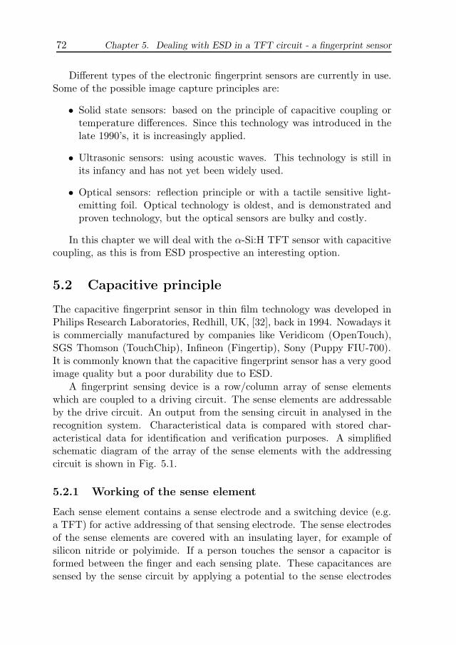
72 Chapter 5. Dealing with ESD in a TFT circuit - a fingerprint sensor
Different types of the electronic fingerprint sensors are currently in use.Some of the possible image capture principles are:
• Solid state sensors: based on the principle of capacitive coupling ortemperature differences. Since this technology was introduced in thelate 1990’s, it is increasingly applied.
• Ultrasonic sensors: using acoustic waves. This technology is still inits infancy and has not yet been widely used.
• Optical sensors: reflection principle or with a tactile sensitive light-emitting foil. Optical technology is oldest, and is demonstrated andproven technology, but the optical sensors are bulky and costly.
In this chapter we will deal with the α-Si:H TFT sensor with capacitivecoupling, as this is from ESD prospective an interesting option.
5.2 Capacitive principle
The capacitive fingerprint sensor in thin film technology was developed inPhilips Research Laboratories, Redhill, UK, [32], back in 1994. Nowadays itis commercially manufactured by companies like Veridicom (OpenTouch),SGS Thomson (TouchChip), Infineon (Fingertip), Sony (Puppy FIU-700).It is commonly known that the capacitive fingerprint sensor has a very goodimage quality but a poor durability due to ESD.
A fingerprint sensing device is a row/column array of sense elementswhich are coupled to a driving circuit. The sense elements are addressableby the drive circuit. An output from the sensing circuit in analysed in therecognition system. Characteristical data is compared with stored char-acteristical data for identification and verification purposes. A simplifiedschematic diagram of the array of the sense elements with the addressingcircuit is shown in Fig. 5.1.
5.2.1 Working of the sense element
Each sense element contains a sense electrode and a switching device (e.g.a TFT) for active addressing of that sensing electrode. The sense electrodesof the sense elements are covered with an insulating layer, for example ofsilicon nitride or polyimide. If a person touches the sensor a capacitor isformed between the finger and each sensing plate. These capacitances aresensed by the sense circuit by applying a potential to the sense electrodes

5.2. Capacitive principle 73
row
driver
circuit
column multiplexers + amplifiers
TFT switch
capacitorelectrode
Figure 5.1: A simplified schematic diagram of the sense elements together withassociated addressing circuitry.
and measuring charging characteristics. Depending whether a ridge or avalley of a finger touches the sensor surface, the capacitor will have a higheror a lower value. A schematic representation of a sense element is shown inFig. 5.2. The pixel plate is precharged to the value Vp. The capacitance of
Cint
OPAMP
prechargeTFT
readTFT
Vp
insulator
metal pad
fingerridge
dS
Q =Cpix pix Vpx
Figure 5.2: Schema of the capacitive fingerprint sensor.
the pixel is determined by the pixel plate area S and the distance betweenthe pixel plate and the finger d. The amount of charge at the pixel plateis proportional to the precharge voltage and the pixel capacitance, Qpix =Cpix × Vp. An operational amplifier with capacitive coupling is used to

74 Chapter 5. Dealing with ESD in a TFT circuit - a fingerprint sensor
integrate the charge. The output current is further handled by columnmultiplexers.
5.2.2 Fabrication of the capacitive fingerprint sensor
We made the capacitive fingerprint sensor based on thin film technology.The sensor is based on the bottom gate (inverted-staggered) α-Si:H TFT.The TFT’s were n-channelled, with a silicon-nitride gate insulator. Aschematic cross-section of a fingerprint cell is given in Fig. 5.3. As thethin film technology is used in well established technologies such as liquidcrystal display devices, and as such it is described well (see for example[71]), here the technology of making the capacitive fingerprint sensor willbe described only briefly.
TFT drain(column)
TFT source(capacitor plate)
substrate
TFT gate(row)
Si Nx y
-Sipassivation layer
Figure 5.3: Cross section of a pixel in the capacitive fingerprint sensor.
The fabrication process involves six photolithographic processes. Theseprocesses are listed in Table 5.1. Fig. 5.4 shows diagrammatically how the
mask layer material thickness [nm]1 gate metallisation Al 3002 etch stop SiNx 3503 drain and source implantation α-Si:H 3004 opening bottom metallisation layer SiNx 3005 top metallisation Al/Mo 3006 passivation SiNx 350
Table 5.1: TFT process flow with layer materials and thicknesses.
amorphous silicon TFT (coupled gate TFT, as used in the ESD protectionstructure) are fabricated.

5.2. Capacitive principle 75
gate metaldeposition
photolithographymask 1/etch
gate insulator,a-Si, etch stopdeposition
photolithographymask 2/etch
sacrificial Al/Modeposition andimplantation
etch, photolithog.mask 3/etch,mask 4/etch
drain/sourcemetal deposition
photolithographymask 5/etch
Figure 5.4: Coupled gate amorphous silicon thin film transistors fabrication pro-cess. Note that the last (passivation) photolithographic step is skipped.

76 Chapter 5. Dealing with ESD in a TFT circuit - a fingerprint sensor
As substrate material we used a Si wafer with a thick (1 µm) layer ofthermally grown SiO2. For the deposition of Al and Mo we chose sputter-ing. For the deposition of amorphous silicon and silicon nitride we usedPECVD (Plasma Enhanced Chemical Vapour Deposition). The depositiontemperature was 250 oC and the discharge frequency 13.56 MHz. Threelayers (SiNx as the gate dielectric, α-Si:H as the TFT channel and SiNx asthe etch stopping layer, protecting the channel from the following etchingprocesses) are deposited without breaking the vacuum. Wet etching wasused for etching of all layers, except for the second metallisation layer madewith Molybdenum. To make a highly doped α-Si:H for the source and draincontacts, ion implantation through a thin (10 nm) Al layer, or 20 nm Molayer was used. Implantation through Mo layer produced a better contact.We implanted both phosphorus and arsenic. Phosphorus implanted TFT’sgave lower contact resistance. We also made a variations with the dose andenergy when implanting phosphorus in order to optimise the implantationparameters for source/drain contacts. The devices were annealed at 280 oCfor 1 hour.
5.2.3 Characterisation of α-Si:H and SiN:H films
The thicknesses of the films are determined by spectroscopic ellipsometry.The thickness of the α-Si:H layer is estimated at 295 nm (mean value) andthe thickness of the SiN:H layer is estimated at 373 nm. Also the refractiveindex of SiN:H was measured and it showed the value of 1.71, which impliesthat the quality of the SiN:H is relatively good, as the value of the refractiveindex of the stoichiometric silicone nitride is about 2.
The structure of the α-Si:H layer has been verified by X-Ray Diffraction(XRD). Fig. 5.5 shows the measured XRD spectra of α-Si:H before andafter thermal annealing at 280 oC during 1 hour. We see that there areno visible spots of the polycrystalline Si on XRD data. Scattering fromvery small “pre-crystalline” areas is visible. There are no visible effects ofannealing on the state of material.
The composition of the SixNy:H layer has been determined by X-rayPhotoelectron Spectroscopy (XPS). The results show that the ratio betweensilicon and nitride is Si:N=1:1. The stoichiometric silicon nitride would haveSi:N=1:1.33. The result implies that the composition of the silicon nitridecould be improved. The presence of hydrogen is also determined by XPS.Hydrogen is found in 12.5 %. The target value is 14%, so this could beimproved as well.

5.2. Capacitive principle 77
Amorphous halo
Figure 5.5: XRD scan of α-Si:H layer before and after thermal annealing.
5.2.4 Electrical measurements of deposited structures
On the wafer with a fingerprint sensor a number of testing structures , suchas TFT’s and capacitors, ESD protection chains, etc. was deposited in orderto fully understand the performance of the fabricated sensor. Electricalmeasurements performed on these testing TFT’s and on a pixel in the sensormatrix will be described in this section. Electrical measurements on the ESDprotection chains will be shown in section 6.4.
TFT’s with different W/L ratios were deposited. In Fig. 5.6 and 5.7measured output and transfer characteristics of a TFT with W/L=100µm/12 µm are shown. From the measured characteristics electron mobilityand threshold voltage are calculated. The threshold voltage is determinedfrom the interception of linear fit of the linear part of the transfer character-istic in the linear regime of working with the x-axis (VD=0.1 V). The valueof the threshold voltage for the given TFT (Fig. 5.7) is 2.8V. From thesame linear fit of the transfer characteristic in the linear regime of working,the field-effect mobility in linear regime µl is determined by Eq. 1.3. Thecalculated value is µl=0.37 V/cm2. The field-effect mobility in the satura-tion regime µs is calculated by fitting a straight line through
√ID(VG) curve
measured in the saturation regime under VD=10 V. The µs is 0.26 V/cm2.For an ideal transistor, the field-effect mobilities calculated in both the lin-ear and the saturation regime should be equal. But due to the neglectionof the series resistance and also due to imperfect linear fitting a mismatchbetween µl and µs happens in practice.
The electrical characteristics of a pixel of the fingerprint sensor matrixmeasured before it was passivated are shown in Fig. 5.8. The figure shows

78 Chapter 5. Dealing with ESD in a TFT circuit - a fingerprint sensor
0 5 10 15 20
0
1
2
3
VG=20V
VG=15V
VG=10V
VG=5V
VG=0V
Dra
incur
rent[
A]
Drain voltage [V]
Figure 5.6: Output characteristics ID/VD under different gate voltages VG=0, 5,10, 15, 20 V of a TFT with W/L=100/12.
-10 -5 0 5 10 15 200.00
0.01
0.02
0.03
0.04
Dra
incurr
ent[
A]
Lin
ear
Gate voltage [V]
0
400
800
1k
2k
2k
VD=0.1V
VD=10V
Sqrt(D
rain
curre
nt[
A])
Satu
ratio
n
Figure 5.7: Transfer characteristics ID/VG under different drain voltages VD=0.1,10 V of a TFT with W/L=100/12.

5.3. Description of the ESD problem 79
0 2 4 6 8 10 12
0.00
0.05
0.10
0.15
VG=10V
VG=5V
VG=0V
Dra
incurr
ent[
A]
Drain voltage [V]
Figure 5.8: Output characteristics of a TFT switch in the fingerprint sensor ma-trix.
that the TFT in the matrix does operate as a switch. The dimensions ofthe TFT’s in the matrix are W/L=21 µm/8 µm and therefore the level ofthe drain current is proportionally lower then in Fig. 5.6.
5.3 Description of the ESD problem
In a capacitive fingerprint sensor a possible ESD zap is applied either di-rectly to the capacitive sensing element by the person who is using it orduring the assembly process by a machine. The latter problem is success-fully solved (for more information see Section 6.1) using the diode/TFTchains, and shortening all columns and rows during the manufacturing.
In the case when an ESD zap is applied directly to the sensing element,it is very difficult to find a good solution to protect the circuit. Under ESDstress, a possible current path goes through the top capacitance down tothe ground Fig. 5.9). The elements in this path that have to be protectedagainst ESD are:
1. the capacitor2. the column ”read” TFT3. the amplifier circuits.The most difficult task is to make the capacitor (actually the top dielec-
tric layer) ESD insensitive. The idea is that the top layer must not be fullyinsulating. A resistive path must exist.

80 Chapter 5. Dealing with ESD in a TFT circuit - a fingerprint sensor
One solution that comes to mind immediately is to construct protectionrings, i.e. walls of a conductive material connected to the ground aroundeach pixel. These walls are generally obtained by gold electroplating inorder to prevent oxidation [34] or of copper encapsulated by ruthenium,which is well known as a contact material and whose oxide is conductive[51]. This solution would certainly protect the sensor against the ESD up toa certain level, but it will introduce some additional problems. First is thatthe number of photolithographic masks will be increased, making the sensormore expensive (for applications like mobile phones it is very important tokeep the price low). In some cases it can cause water penetration from thesensor surface to the active area [34].
Another possible solution is to make good choice of material used forthe top dielectric layer. It should satisfy three conditions: to give ESDprotection, to avoid charge loss in the capacitor and to not allow reductionof effective resolution. The easy solution for the last condition is goodchoice of the capacitor dimensions. In case the dimensions of the capacitorare: area A = 50µm x 50µm, insulator thickness d = 500nm and distancebetween two cells x = 10µm then the ratio of resistances in lateral andvertical direction is Rs/Rp = 1600. This ratio should provide good effectiveresolution of the sensor, as the lateral component of the current is almostnegligible. Also, it may be possible to use material which is conductive inonly one, for example vertical and not in lateral direction.
To avoid charge loss it is desirable to keep the insulator thin. This maycounteract to the ESD robustness of the layer. The effect of the resistivelayer may be presented as a parallel connection of a capacitor and a resis-tor, as it is shown in Fig. 5.9. Considering ESD conditions, the resistanceRp will take the ESD current (the current through Rs may be neglected assufficiently lower). We have to determine how large this resistance shouldbe in order to protect the surface layer and also not to influence too muchthe operation of the circuit under both DC and ESD conditions. There aretwo issues that have to be mentioned. First is that the current throughthe surface layer will produce power dissipation, P = V 2
Rp/Rp, which leadsto heating. To simulate thermal behaviour of the surface layer would bestraightforward using Silvaco tools, if the material (which will be used forthe capacitor) were included in the simulator. We can also translate the con-clusions from our experience with thermal simulations on TFT’s stresses inthe drain, Chapter 3. If the resistive layer is a moderate thermal conductorit can be expected that the peak of the temperature distribution will beat the surface, and that the peak of the temperature in the resistive layer

5.3. Description of the ESD problem 81
CFA
Vp
prech
read
CFA
Vp
prech
read
Rs Rs
RpRp
P1
P2
Figure 5.9: Current path in the capacitive fingerprint sensor.
will be lower when the layer is thicker (Rp higher). On the other hand, thisresistive material could be a very poor thermal conductor or a very goodthermal conductor. In both cases the thickness of the resistive layer wouldnot play a role at the temperature distribution, as in the former case thetemperature would be localised at the surface, and in the latter case thetemperature would be transfered without losses to the rest of the sensor.Another issue important for ESD protection is that the current through theresistor Rp should produce a voltage drop sufficiently large to provide thatthe voltage on the TFT switch, which is directly connected to the surfacelayer via a metal plate, is never higher then the breakdown voltage of theTFT gate dielectric layer? In our case that is 330 nm SixNy, having around350 V breakdown voltage. In this way the TFT switch would be protectedand the element P1 in Fig. 5.9 would not be needed.
Considering the ESD protection under the TFT switch (Fig. 5.9), itwould be necessary to design the protection devices that will provide thepath to the ESD current. It seems to be the second most important issue,after setting a proper material for surface. If this part of the sensor wouldbe realised also in amorphous silicon thin-film technology, choice of theelementary structures for building a ESD protection would be very limited.The devices that one could use for protection elements P1 and P2 are onlynon-snapback type of protection structures, like:
• chains based on TFT’s used as diodes - made by coupling the gate

82 Chapter 5. Dealing with ESD in a TFT circuit - a fingerprint sensor
and the drain directly together. This structure is already successfullyused for each of the input and output terminals at the edge of theglass substrate. A more detailed examination of a similar structurewill be presented later in the chapter 6.
• TFT’s - as this devices never go to snapback, they can be used onlyin a non-breakdown mode. Normal MOS design can be used, as wellas GC TFT (Gate coupled TFT) (Fig. 5.10). Considering transientregime, an appropriate choice of R and C would help to provide thatTFT would turn-on only under a ESD zap.
• It would be also possible to use TFT’s with a thick gate dielectric,to increase the breakdown voltage. A specific structure based on thinfilm technology could be designed and implemented for the protectionelement P1/P2 in Fig. 5.9.
• High voltage TFT. For the switch a high voltage TFT (with the drainextension LD, as shown in Fig. 5.11) could be used. It would be usedin connection to the resistor Rp with its drain, and would ensure thatthe electric field in the gate dielectric is such that TFT can withstandhigher voltages. Instead of typical breakdown voltage of 350 V, itcould be easily increased up to 600 V, as reported in [25].
C
R
Figure 5.10: Gate coupled TFT.
5.3.1 ESD robust concept: resistive or pressure sensing?
As it was already explained in the previous section, the simplest (fromthe manufacturing point of view) way to protect the capacitive fingerprint

5.3. Description of the ESD problem 83
metalic gate
source and drain contacts
n drain+
n source+ -Si
SiNx
drain extension LD
Figure 5.11: High voltage TFT.
sensor from the electrostatic charge of the human operating the sensor is toprovide a current path to the ground introducing a material which wouldprovide both good dielectric properties to allow for the capacitive sensingand good resistive properties for giving the “low”-resistive path for the ESDcurrent [6]. It is a difficult task to optimise the material properties to satisfyall necessary conditions.
Another possible solution is to change slightly the concept of the sensorand to use resistive instead of capacitive sensing. The basic schema of thecircuit could remain similar as in Fig. 5.9. Instead of the integrator anoperational amplifier would be used for the amplification of the signal. Theproblem with the resistive sensor is that the current path would have tobe closed through the human body. Although that is an almost negligibleeffect, many people would object to this approach.
The idea of the resistive fingerprint sensor could be also combined withthe pressure sensing, using the piezo-resistive effect. In the piezo-resistiveeffect the electrical resistance of silicon changes with external pressure. Atconstant temperature, the resistance R of a semiconductor element of areaA, length l, resistivity ρ is R = ρ l
S . When the element is strained (e.g.pressed) the resistivity changes by an amount:
∆R = (δR
δl)∆l + (
δR
δρ)∆ρ+ (
δR
δA)∆A =
ρ
A∆l +
l
A∆ρ+
ρl
A2∆A (5.1)
∆R
R=
∆l
l+
∆ρ
ρ− ∆A
A(5.2)
A CMOS compatible micromachined tactile fingerprint sensor has been

84 Chapter 5. Dealing with ESD in a TFT circuit - a fingerprint sensor
reported in [39]. It would also be possible to use this approach in amor-phous and polysilicon thin film technology. Piezoresisistive properties inpolysilicon are affected by microstructure (fabrication process) and electri-cal properties (doping level). Unfortunately the micromachining part of thecircuit would be quite expensive. The rest of the circuit is very simple,composed from passive components only. This concept is ESD robust, asthe micromachining part, which is in direct contact with the human body,is not electrically active.
5.4 Summary
We have manufactured a capacitive fingerprint sensor with α-Si:H TFT’sused as switches. The design, the process flow and the test measurementshave been showed in this chapter. The sensor is used for an theoreticalESD analysis. The behaviour under an ESD stress has been described, andpossible ESD solutions have been discussed. Several ideas for an ESD robustfingerprint sensor have been proposed.

Chapter 6
TFT based ESD protection
This chapter will be focused on testing and analysing of ESDprotection devices based on thin film transistors. A number ofvarieties of protection structures made with coupled gate TFT’swill be tested. Circuit simulations of a TFT matrix without andwith ESD protection will be presented. Based on the testing andthe simulation results a proposal of how to improve ESD protec-tion in TFT circuits will be given.
6.1 Introduction
The ESD protection of a TFT based electrical circuit has to be efficient dur-ing the manufacturing and the application of the circuit from all potentialsources of the creation of electrostatic charge. It should be noted that thedesign of any ESD protection is focused in two directions. First, electro-static charging has to be prevented and second, the design of the protectionstructure should be optimised in such a way that there is no damage upto a certain stress level, the functionality of the product is not affected toomuch and it should not use to much area.
In this thesis we will not discuss preventing of the electrostatic charging.Only a few general remarks should be noted. TFT LCD’s are built froma multi-layer structure on a glass substrate. Most of the processes in theTFT LCD’s production combine movements, friction and separation of thisglass substrate with other materials. Those processes are the cause for thegeneration of an electric charge at the surface of the glass. One of the maingenerators of the electric charge in the TFT LCD production process is theact of separation of the glass substrate from a metal surface (chuck) on which
85

86 Chapter 6. TFT based ESD protection
it is laying during processing. The separation of the glass from the metalchuck creates an amount of electric charge in the glass according to thetriboelectric theorem. The best method to prevent this type of ESD dangerin to prevent it on-line [28], but that task will not be analysed here. Oneother way to prevent the electrostatic charging during the manufacturing isto short all row electrodes and all column electrodes by a shorting bar. Thatwould protect the displays during the processing, although after the scribeand break process, when the shorting bars are separated from the activematrix, the glass plates become very vulnerable to ESD and this substratecan be easily charged during handling. One way to reduce the problem isthe coverage of unused glass surface by dummy metal. The dummy metalcreates equipotential surfaces and prevents the glass from being charged.
In this chapter the attention will be focused on the ESD protection,by gaining knowledge by measurements, modelling and simulations. Theproblem will be discussed in general, and similar analysis can be applied forany TFT matrix used in, for example, liquid crystal displays, for telecomapplications, in automotive industry or in sensors. Each of these applica-tions has some specific working conditions that has to be taken into accountwhen one is designing an ESD protection circuit. These conditions will beshortly described. Knowing the conditions in which the circuit will operatewill help to determine which method should be chosen for ESD testing andwhich criteria the ESD protection circuit has to satisfy.
TFT’s used in telecom application (e.g. mobile phones) suffer from anadditional restriction when we are talking about ESD protection. Namely,there is always a significant leakage through the ESD ring at the operationalvoltage. And in mobile phones power consumption is very important [41].Therefore the leakage currents that are allowed in LCD’s where a constantpower supply is present are actually not allowed in telecom applications.
TFT’s are also often used for displays in car industry, where they arebuilt in the control panel. High quality of these displays is requested, con-sidering the price of the car. Acceptable number of pixel defects is very low.ESD protection is in this application very important [72].
TFT’s used for applications in sensors often have some very specificrequests. For example, the problem of the capacitive fingerprint sensor isalready described in Section 5.3.
A general solution will not be given in this chapter, as the problem withall its variations is too complex, but a number of relevant recommenda-tions that should be taken into account while designing a TFT based ESDprotection structure will be given.

6.2. Basic of ESD protection design 87
6.2 Basic of ESD protection design
A successful ESD solution is not trivial. A number of good individual ESDcomponents should be put together so that they cover all possible ESD zapconditions. Two possible approaches can be used for ESD protection design:
1. Random path approach: To find experimentally (by means of ESDtesting + failure analysis) the Random Path of ESD current. When theweakest link is found, the layout is fixed and the new circuit is forwardedto the next iteration of testing and failure analysis. Hopefully, after severaliterations of testing and re-designing, one could expect that desired ESDprotection will be realized.
2. Current path approach: To provide a designated path by which ESDcurrent can be discharged. The designated path has very low impedance,comparing with the other possible current paths. Designing the currentpath, it is important that the remaining voltage between the pins is suffi-ciently low, such that dielectrics are not damaged. This current path usuallyconsists of devices in a working chain. In crystalline devices, a device usedin this chain might be either breakdown-type (such as grounded gate MOS)or non-breakdown type device. As amorphous silicon TFT’s do not work asbreakdown devices (for example, crystalline MOS devices are used in snap-back regime - when parasitic bipolar transistor is switched on and they canhandle large current while keeping voltage constant at a certain value), theonly possibility is to use non-breakdown devices, which operate near theirnormal operating regime and are therefore easy to predict and simulate.
In this chapter, we will combine the two methods. First the TFT circuits(LCD) will be tested by means of TLM and the failure analysis will beperformed in order to find the random path of ESD current. Further, theTFT matrix will be modelled and simulated in the circuit simulator Pstar.Changing the design in the simulated model, a wanted ESD current path willbe created. The current path approach is more designable and systematic,and therefore is considered as better, and in this section we will put moreattention on this solution.
6.3 Testing of ESD protection structures in TFTAMLCD’s
In this section the results of ESD (TLM) testing on α-Si:H TFT based re-flective AM LCD’s, manufactured by Philips Mobile Display Systems, Kobe,Japan, will be presented and discussed. The displays are manufactured for

88 Chapter 6. TFT based ESD protection
ESD guard band
VS
V (n)G
V (n-1)G Cst orage
TFT switch
Vcom
Cst orage
TFT switch
Vcom
Figure 6.1: Electrical scheme of the display with the protection band type A.
use in telecom applications and handheld computers. One of the majorcauses for display failures during manufacturing is ESD (1-2 % out of total10 %). It has been found that the leakage current of the ESD protectionring during normal operation of the display gives rise to power dissipation.Three types of reflective TFT panel are evaluated (A, B, C) in order to findout which one has the best performance from the point of leakage currentsand also from the point of ESD protection.
In type A we have two types of ESD protection. The electrical schemeof the display A is shown in Fig. 6.1. The ESD protection of the gate linesconsists of a guard band to which all gate are connected via TFT’s thathave the gate connected to the drain (gate coupled TFT’s). The structurehas two TFT’s that are connected in a parallel connection from the gateline to the guard band. There is one TFT in each direction so that if thepotential on a particular line exceeds a certain value one of the TFT’s willturn on giving a leakage path. This structure is called “Single TFT, singlering, double sided”. A drawback here is that the TFT’s turns on at arather low voltage so that the ESD guard band will give a leakage current,which corresponds to the power dissipation of the order of 1mW in normaloperation. The ESD protection of the source lines has two TFT’s in a serialconnection from the source line to the guard band. A disadvantage of thisstructure that it provides protection for only one (positive) polarity of thestress pulse. This protection is named “Double TFT, single ring, singlesided”.
To reduce the leakage current these structures have been modified. In

6.3. Testing of ESD protection structures in TFT AMLCD’s 89
ESD guard band
VS
V (n)G
V (n-1)G Cst orage
TFT switch
Vcom
Cst orage
TFT switch
Vcom
Figure 6.2: Electrical scheme of the display with the protection band type B(double TFT protection between gate or source bus and guard band).
type B two series of two TFT’s in a parallel connection are used. The ideais that if the voltage is shared between two TFT’s, then during normaloperation each of the TFT’s will stay off. During an ESD event they willalso share the stress, which also can improve the ESD protection. Thescheme of the display B is shown in Fig. 6.2. This type of protection iscalled “Double TFT, single ring, double sided”.
Type C splits the guard band into two, as shown in Fig. 6.3. The TFT’sbetween a gate/source bus and the guard band 1 are activated if a positivestress is applied on the bus, and the TFT between a gate/source line and theguard band 2 is activated if a negative ESD stress is applied. This structureis named “Double TFT, double ring, single sided”.
Testing of the displays will be carried out in two steps, first the wholedisplay matrixes will be tested in order to find out the breakdown voltage,the failure spot and if possible to determine the random path of ESD cur-rent. Second, the ESD protection structures itself will be tested apart ofthe display matrix in order to clarify their performance under ESD biasingconditions.
6.3.1 TLM testing of the display matrix
All three display types are tested by means of a TLM tester, in order to findout which structure is most effective in suppressing ESD effects. First theresults of the testing of the panel will be presented. TLM measurementsshowed a breakdown voltage of around 380 V. Stressing by means of TLM

90 Chapter 6. TFT based ESD protection
ESD guard band 1
VS
V (n)G
V (n-1)G Cst orage
TFT switch
Vcom
Cst orage
TFT switch
Vcom
ESD guard band 2
Figure 6.3: Electrical scheme of the display with the protection band type C(double guard band).
voltage was continued long after breakdown in order to make the failure spotclearly visible. The pre-breakdown degradation is not known, as the leakagecurrent measurement did not show any increase prior to the breakdown.After TLM testing was finished, the displays were optically examined inorder to find the breakdown spot. After examinations under microscope,it could be concluded that always the TFT protection structures and onlyin one case the pixel TFT in the matrix are broken down. The conclusionis that the protection structure breaks down first. Only in the case whenTLM voltage is continued several times after the breakdown the TFT in thedisplay matrix will be affected.
TLM measurements were continued on the panel B (Double TFT, singlering, double sided). Breakdown voltage was identified by the TLM measure-ments, but in several cases it was difficult to observe the breakdown spoton the panel. If it was possible, then often the breakdown spot was locatednot in the TFT active area but at the line crossing between the stressedgate/source line and the guard band.
Finally, the panel C (Double TFT, double ring, single sided) was mea-sured. The breakdown voltage was around 380 V, and the breakdown spotcould not be identified in the TFT area, but only at the crossing of thestressed gate/source line and the guard band.
In the measured samples, the breakdown spot is found sometimes inthe protection structures, sometimes in the circuit; sometimes in the TFTactive area, sometimes in the metallisation lines crossing. One example of

6.3. Testing of ESD protection structures in TFT AMLCD’s 91
Figure 6.4: Protection structures left and right from the stressed gate line arebroken down.
the failure spot (a broken TFT in the protection structure), measured onthe display type A, is shown in Fig. 6.4.
The breakdown voltages are at the expected level for the given gate di-electric thickness and the channel length. It implies that the breakdown isdielectric breakdown, which appears either in the TFT active area or at thecrossings of the bottom and top metallisation layers (gate and source lines).There is no difference in the protection under the TLM stress between dif-ferent protection structures in the TLM breakdown voltages. A comparisonof measured TLM breakdown voltages is given in Fig. 6.5. The questionarises why the pixels in the matrix are not protected for the voltages higherthen 380 V. Also, it is not clear why there is no difference in the breakdownvoltages whithin the different structures. Whether the ESD structures donot work as they should, or if they do work as planned, then the design ofprotection is not good. To answer this dilemma, first the protection ele-ments will be tested and second, the design of the ESD protection will bere-considered using Pstar simulations.
6.3.2 Testing of ESD protection structures
The ESD protection structures are tested to study their ESD behaviourwithout any disturbance of the matrix. The structures are firstly measuredwith a Parameter Analyser HP4145B in order to determine their regime ofworking/switching on, and later the protection structures are ESD tested

92 Chapter 6. TFT based ESD protection
0 50 100 150 200 250 300 350 400 450
0.00
0.02
0.04
0.06
0.08
0.10
0.12
0.14
0.16
0.18
TLM
cur
rent
[A]
TLM voltage [V]
single TFT single band single TFT double band double TFT single band
Figure 6.5: Comparison of measured TLM breakdown voltages for protectionstructures A, B, C.
by means of a TLM tester.The results of the measurements by means of the Parameter Analyser
are shown in Fig. 6.6. The voltage is increased from 0 to 100 V and thecurrent is measured. Usually, when testing protection devices, current isforced, as a snapback cannot be studied in a voltage force mode. For thesedevices however, there is no snapback. The protection elements from differ-ent display types are presented together in order to compare their working.The plot shows that the display type A “Single TFT, single ring, doublesided” switches on first and produces the highest current. The current char-acteristics is degraded (saturated at the level of approximately 1 mA) after60 V. The display type C “Double TFT, double ring, single sided” switcheson also very fast and works well until 80 V when it also starts to saturate.The display type B “Double TFT, single ring, double sided” switches onconsiderably later, and does not go into the high current regime or satura-tion.
To have a clearer explanation of working of these ESD protection struc-tures, they were tested in the following way. The stress is applied either onthe gate or source line, while the other line (source or gate) was floating,and the protection ring was grounded. In this case we expect to test theprotection device itself. The result of the measurements are as follows.
As for the display type A the ESD structure for gate line differs fromthe ESD protection structure for the source line, therefore the results oftesting will be plotted separately for each of this two structures, Fig. 6.7“Single TFT, single ring, double sided” and Fig. 6.8 “Double TFT, single

6.3. Testing of ESD protection structures in TFT AMLCD’s 93
0 20 40 60 80 100
1E-7
1E-6
1E-5
1E-4
1E-3
I [A
]
V [V]
'Single TFT, single ring' 'Single TFT, double ring' 'Double TFT, double ring'
Figure 6.6: Measurements of the protection structures by means of ParameterAnalyser HP4145B.
ring, single sided”. There is a difference between these two structures in themeasured TLM breakdown voltages. The structure with two TFT in serieson one side of the source line showed the breakdown voltage of 260 V, andthe structure with one TFT connected with its gate and drain and one TFTconnected with its source between the gate line and the protection bandshowed the breakdown voltage of approximately 160 V. Also the leakagecurrents were monitored during the TLM stressing. The leakage currentmeasured before breakdown from the side of the source line (two TFT in aserial) were in order of 2 · 10−11 A, and the leakage current measured fromthe gate side (two single TFT’s) were in order of 5 · 10−10 A.
The display type B “Double TFT, single ring, double sided”, has equiv-alent structures from both gate and source bias line. Therefore only theresults of testing protection structures from the source line will be shown.It can be seen from the Fig. 6.9 that the breakdown voltage under TLMstress is considerably higher then in the display A, it is approximately 330V. The leakage current before the breakdown is in order of 3 · 10−10 A.
Finally, the display type C, “Single TFT, double ring, single sided”showed a TLM breakdown voltage of 310 V and the leakage current beforethe breakdown of 3 · 10−11.
The conclusion from the measured samples is that the single TFT hasa lower TLM breakdown voltage then the serial connection of two TFT’s.There is a big difference in the measured leakage current as well. A compar-

94 Chapter 6. TFT based ESD protection
0 50 100 150 200 250
0.00
0.02
0.04
0.06
0.08
0.10T
LM c
urre
nt [A
]
TLM voltage [V]0.00 0.02 0.04 0.06 0.08 0.10
1E-10
1E-9
1E-8
1E-7
1E-6
1E-5
Leak
age
curr
ent [
A]
TLM current [A]
Figure 6.7: TLM current and leakage current measurements during TLM stresson “Single TFT, single ring, double sided” structure.
0 50 100 150 200 250
0.00
0.02
0.04
0.06
0.08
0.10
TLM
cur
rent
[A]
TLM voltage [V]0.00 0.02 0.04 0.06 0.08 0.10
1E-11
1E-10
1E-9
1E-8
1E-7
1E-6
Leak
age
curr
ent [
A]
TLM current [A]
Figure 6.8: TLM current and leakage current measurements during TLM stresson “Double TFT, single ring, single sided” structure.
0 50 100 150 200 250 300 350 400
0.00
0.02
0.04
0.06
0.08
0.10
0.12
TLM
cur
rent
[A]
TLM voltage [V]0.00 0.02 0.04 0.06 0.08 0.10
1E-10
1E-9
1E-8
1E-7
Leak
age
curr
ent [
A]
TLM current [A]
Figure 6.9: TLM current and leakage current measurements during TLM stresson “Double TFT, single ring, double sided” structure.

6.3. Testing of ESD protection structures in TFT AMLCD’s 95
0 50 100 150 200 250 300 350
0.00
0.05
0.10
0.15
0.20
TLM
cur
rent
[A]
TLM voltage0.00 0.05 0.10
1E-11
1E-10
1E-9
1E-8
Leak
age
curr
ent [
A]
TLM current [A]
Figure 6.10: TLM current and leakage current measurements during TLM stresson “Double TFT, double ring, single sided” structure.
ison of the results of the TLM testing on ESD protection structures isolatedfrom the display matrix is shown in Table 6.1.
ESD Breakdown Leakage current Turn-on voltageprotection voltage (between TLM pulses, (correspondingstructure under TLM before breakdown) I = 100µA)1. SSD 160 V 500 pA 25 V2. DSS 240 V 20 pA 36 V3. DSD 330 V 300 pA 120 V4. DDS 310 V 30 pA 56 V
Table 6.1: Comparison of ESD protection structures. Structure 1. SSD: SingleTFT, single ring, double sided; Structure 2. DSS: Double TFT, single ring, singlesided; Structure 3. DSD: Double TFT, single ring, double sided; Structure 4. DDS:Double TFT, double ring, single sided.
If we now compare the breakdown voltages of the tested ESD protectionstructures (Table 6.1), we can conclude that the breakdown voltages of thestructures 1, 3 and 4 fulfil the expectations, as the single TFT structure (1.SSD) has the lowest breakdown voltage. Two TFT’s in series (structures 3.DSS and 4. DDS) have a breakdown voltage that is almost two times higher(that is desirable and as expected). Surprisingly, the breakdown voltage ofthe structure 2. DSS does not obey the rule:
VBR(TFT chain) = No. TFT’s · VBR(single TFT) (6.1)
The breakdown voltage here is decreased due to some influence of the par-

96 Chapter 6. TFT based ESD protection
ESD guard band
VS
V (n)G
V (n-1)G
TFT switch
TFT switch
Figure 6.11: TFT’s chains in the fingerprint sensor.
asitic structures, as we know that the TFT’s are the same in all structures.Of course one wants to have the breakdown voltage as high as possible
and increasing the number of TFT’s we could improve it, but increasingthe number of TFT’s would also lead into the same increase of the turn-onvoltage. In other words, one wants to have turn on voltage optimised: ithas to be higher then the display operational voltage (otherwise the leakageis too much), but on the other side not too high.
The leakage current, measured at 20-25V (operational voltage for thedisplay), should be kept as low as possible, as mentioned earlier. It can benoticed that the excessive leakage comes always from the symmetric chain.Actually, if the symmetric chain is split in two guard rings, the leakage isdramatically decreased. It is not quite clear why the leakage is related withthe design/geometry of basically the same protection structure, but it isclear that the leakage can be avoided simply by separating the chains.
6.4 Testing of TFT chains in fingerprint sensor
Chains of five TFT’s in a serial connection (Fig. 6.11) are used for each rowand column protection. The chains are connected to a single guard ring 1.Single protection chains were designed on the test part of the sensor. Thechains were built in three variations of TFT’s, with channel width and lengthof 160µm/64µm, 80µm/32µm and 40µm/16µm. The chains were tested,
1The structure described in this section belongs to the same fingerprint sensor asdescribed in the section 5.3.
6.5. ESD stress on the gate of α-Si:H TFT’s 97
applying the stepped voltage up to 100V on the one side of the chain, havingthe other connection grounded. The result of the measurements is shownin Fig. 6.12.
0 20 40 60 80 100
0.0
0.5
1.0
1.5
2.0
2.5
3.0
I [uA
]
V [V]
40/16 80/32 160/64
Figure 6.12: Measured characteristics of TFT’s chains with different channelwidths and lengths.
From the Fig. 6.12 it can be seen that all of the three chains switchon at about the same voltage of 40 V. That is consistent with the mea-sured threshold voltage of a single TFT. The larger TFT’s produce a highercurrent under the same voltage. The current is in the order of µA.
6.5 ESD stress on the gate of α-Si:H TFT’s
In addition to the experiments with the ESD protection structures alreadypresented in this chapter and to the experiments on the drain of a singleTFT presented in Chapter 2, experiments with TLM stress on the gate of asingle TFT are performed for the sake of clarity of the ESD event in a TFTcircuit. When a TFT is exposed to an ESD stress, the zap comes either onits drain/source (TFT’s are symmetrical from this point of view) or on thegate. Stressing on the drain is already explained in the previous chaptersand in this section ESD stressing on the gate will be investigated.
TFT’s with the channel width and length of 100µm/20µm, 75µm/15µmand 40µm/8µm were tested by means of TLM. Between the stresses thetransfer characteristic was measured. The results of these measurements

98 Chapter 6. TFT based ESD protection
are shown in Fig. 6.13 for a series of TLM stress of 500ns applied on aTFT with W/L=100µm/20µm. Any W/L could have been taken as thegraphs are all the same. Apparently the behaviour of tested TFT’s does
0 5 10 15 20
0.0
0.1
0.2
0.3
0.4
0.5W/L=100m/20m
I D[
A]
VG
[V]
40V80V120V160V200V240V280V320V360V400V440V
Figure 6.13: Transfer characteristics of the TFT with W/L=100µm/20µm moni-tored during a TLM series on the gate.
not depend on the channel width or length. Namely, TFT’s with differentchannel widths and lengths gave the same response under the TLM stress onthe gate. This result is logical and was expected. If a TLM stress is appliedon the gate, while the drain and the source are grounded, there is no draincurrent in the channel. On the other side, due to the high gate voltage, theelectric field in the gate insulator is high. If the electric field exceeds thecritical value the dielectric starts to leak and if the field is increased furtherit breaks down. In SiNx the critical field when the leakage current sets in is4-5 MV/cm and the breakdown field is 12 MV/cm. In our TFT’s it meansthat under 240 V TLM stress on the gate the wearing-out of the dielectricsets-in, and the dielectric breaks down at 320 V TLM stress on the gate.These voltages do not depend on the channel length and width but only onthe gate thickness.

6.6. Discussion on improvement of TFT based ESD protection 99
Data input
Gate
scan
1 2 3 ... n
1
2
3
...
m
Data lineStorage cap.
Gate lineLC cap.
TFT
Figure 6.14: Schematic diagram of a TFT LCD.
6.6 Discussion on improvement of TFT based ESDprotection
6.6.1 Modelling and simulation of TFT displays for ESDperformance
The electrical response of the TFT LCD’s without and with ESD protectionunder ESD stress will be modelled and simulated in this section. An imag-inary TFT display is analysed, as presented in Fig. 6.14. It has n columns(data lines) and m rows (gate lines). Therefore n×m pixels of which eachhas a TFT, a storage capacitor Cs and a liquid crystal capacitor CLC . Thestorage capacitor may be present but it does not have to, as it is intendedto improve the retention characteristics of the signal charge [71]. It canbe found in literature in two variations, as from the pixel to the ground orfrom the pixel to the gate line [38]. The display operates one line at a time -video signals are fed to the data lines simultaneously through a data bufferduring the gate turn-on time. The scan voltage pulse applied to a certain(say, i-th) gate line opens the gates of the TFT’s connected to the line. Thesignal voltage is then applied to the pixel electrode of each dot on this gateline.
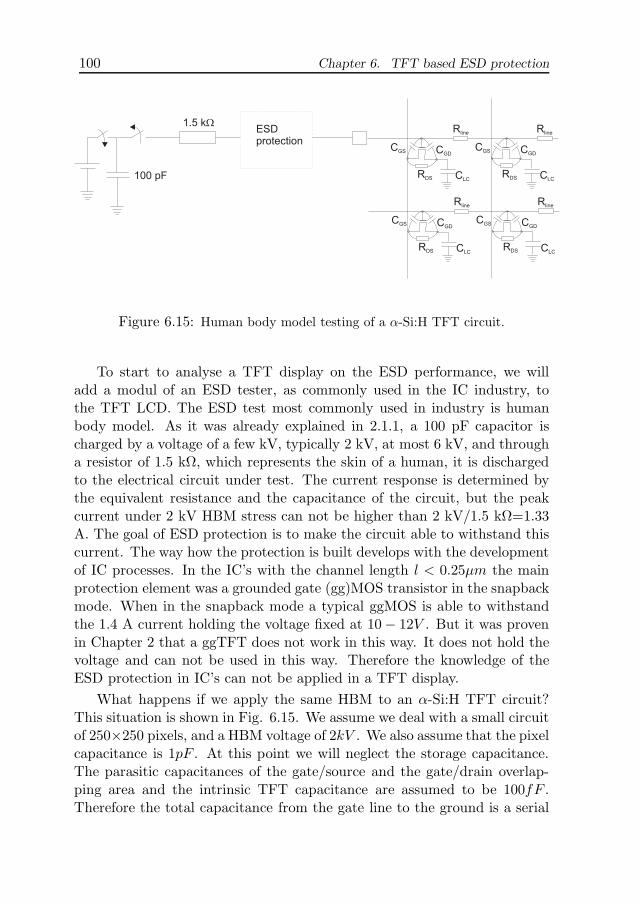
100 Chapter 6. TFT based ESD protection
100 pF
1.5 kESDprotection
CLC
CGDCGS
RDS CLC
CGDCGS
RDS
Rline Rline
CLC
CGDCGS
RDS CLC
CGDCGS
RDS
Rline Rline
Figure 6.15: Human body model testing of a α-Si:H TFT circuit.
To start to analyse a TFT display on the ESD performance, we willadd a modul of an ESD tester, as commonly used in the IC industry, tothe TFT LCD. The ESD test most commonly used in industry is humanbody model. As it was already explained in 2.1.1, a 100 pF capacitor ischarged by a voltage of a few kV, typically 2 kV, at most 6 kV, and througha resistor of 1.5 kΩ, which represents the skin of a human, it is dischargedto the electrical circuit under test. The current response is determined bythe equivalent resistance and the capacitance of the circuit, but the peakcurrent under 2 kV HBM stress can not be higher than 2 kV/1.5 kΩ=1.33A. The goal of ESD protection is to make the circuit able to withstand thiscurrent. The way how the protection is built develops with the developmentof IC processes. In the IC’s with the channel length l < 0.25µm the mainprotection element was a grounded gate (gg)MOS transistor in the snapbackmode. When in the snapback mode a typical ggMOS is able to withstandthe 1.4 A current holding the voltage fixed at 10− 12V . But it was provenin Chapter 2 that a ggTFT does not work in this way. It does not hold thevoltage and can not be used in this way. Therefore the knowledge of theESD protection in IC’s can not be applied in a TFT display.
What happens if we apply the same HBM to an α-Si:H TFT circuit?This situation is shown in Fig. 6.15. We assume we deal with a small circuitof 250×250 pixels, and a HBM voltage of 2kV . We also assume that the pixelcapacitance is 1pF . At this point we will neglect the storage capacitance.The parasitic capacitances of the gate/source and the gate/drain overlap-ping area and the intrinsic TFT capacitance are assumed to be 100fF .Therefore the total capacitance from the gate line to the ground is a serial

6.6. Discussion on improvement of TFT based ESD protection 101
connection of CTFT and CLC , Cpixel = 11/CTF T +1/CLC
= 90fF . The totalcapacitance of the line under test would be a parallel connection of 250 pixelcapacitances with Ctot = 250 · 90fF = 2.27pF . For start, let’s assume thatresistance of the metal line is zero. Therefore the voltage of 2 kV from theHBM capacitor of 100pF would be distributed between the human bodycapacitance and the equivalent capacitance of the matrix. The voltage inthe matrix would be equal to:
Vpixel =CHBM
Ctot + CHBM· VHBM = 1.95kV (6.2)
This is an approximation of the voltage stress that comes to a pixel if thereis no current shunted to the ground. In most often case the number ofpixels in a row is much larger which means that the voltage on a pixelwould be less. Still, the current through the circuit is too low to provide asufficiently high voltage drop on the human body resistor, and the voltageon the line under ESD zap is too high. A current discharge element isneeded, or another way to reduce the voltage. Obviously the problem is notsimple and the parasitics may not be neglected. To answer this questionelectrical simulations are performed and the current of the TFT during andESD stress is calculated. The resistance of the metal line must not beneglected. In this way a transmission line is created which has a very longdelay time. The pulse propagates down the gate line which is representedby the CpixelRpixel circuit, and the rectangular input pulse is delayed anddistorted as it travels along the gate busline [71]. The gate delay is definedas the time when the pulse height at the end of the line reaches 90% of theinput pulse amplitude and it depends on the length of the gate line lg bythe equation:
td ≈ RCl2g (6.3)
The first pixel is therefore first exposed to the ESD stress, and the last pixelsare in this way protected. The prediction is that under the ESD stress themost of the failures is located in the first columns. This is actually confirmedby experiments on the thin film diode displays [4]. It also could be confirmedby means of electrical simulations.
Estimation of parasitic elements
For the electrical simulations an estimation of parasitics of both the metalli-sation and the TFT’s will be introduced. From the modelling point of view,wires have three important characteristics: resistance, capacitance (electri-cal energy) and inductance (magnetic energy). Wires are represented as a
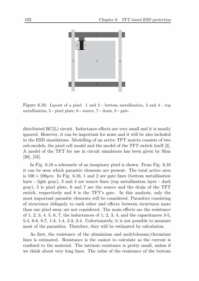
102 Chapter 6. TFT based ESD protection
1
2
3 4
6
5
7
8
Figure 6.16: Layout of a pixel. 1 and 2 - bottom metallisation, 3 and 4 - topmetallisation, 5 - pixel plate, 6 - source, 7 - drain, 8 - gate.
distributed RC(L) circuit. Inductance effects are very small and it is mostlyignored. However, it can be important for noise and it will be also includedin the ESD simulations. Modelling of an active TFT matrix consists of twosub-models, the pixel cell model and the model of the TFT switch itself [2].A model of the TFT for use in circuit simulators has been given by Shur[26], [53].
In Fig. 6.16 a schematic of an imaginary pixel is shown. From Fig. 6.16it can be seen which parasitic elements are present. The total active areais 100 × 100µm. In Fig. 6.16, 1 and 2 are gate lines (bottom metallisationlayer - light gray), 3 and 4 are source lines (top metallisation layer - darkgray), 5 is pixel plate, 6 and 7 are the source and the drain of the TFTswitch, respectively and 8 is the TFT’s gate. In this analysis, only themost important parasitic elements will be considered. Parasitics consistingof structures obliquely to each other and effects between structures morethan one pixel away are not considered. The main effects are the resistanceof 1, 2, 3, 4, 5, 6, 7, the inductances of 1, 2, 3, 4, and the capacitances 3-5,5-4, 6-8, 8-7, 1-3, 1-4, 2-3, 2-4. Unfortunately, it is not possible to measuremost of the parasitics. Therefore, they will be estimated by calculation.
As first, the resistance of the aluminium and molybdenum/chromiumlines is estimated. Resistance is the easiest to calculate as the current isconfined to the material. The intrinsic resistance is pretty small, unless ifwe think about very long lines. The value of the resistance of the bottom

6.6. Discussion on improvement of TFT based ESD protection 103
Al wires is estimated from the equation:
Rpixel = Rlpixel
wAl line= 1.5Ω (6.4)
where lpixel = 50µm is the length of the metal line between two pixels,wAl line = 8µm is the line width. The sheet resistance of the aluminium lineis R = 0.12 Ω
sq . The parasitic resistance of the source bus is estimated inthe similar way to value of Rbus = 40Ω. The drain bus is made of MoCr,which has sheet resistance of R = 1.6 Ω
sq , and the width of the line iswMoCr line = 4µm. The resistance of the pixel plate is 6Ω.
The inductive coupling is much more complex to analyse. Inductancecalculation is based on Maxwell’s equation. The estimate is very difficultbecause it depends on where the currents flow. But the problem in this casewill be reduced, because the inductances are not expected to have muchinfluence in this analysis. The self inductance of a straight conductor withdepth small compared to the length and width can be approximated by [63]:
L =4µm0
Dπ[sinh−1(
l
w)− 1] (6.5)
where µm0 is magnetic permeability of free space 4π10−7H/m.The capacitance coupling is mostly a nearest neighbour issue. The par-
allel plates approximation can be used in most of the cases (always whenthe dimensions of the plates are larger then the distance between them).
C =ε0εrd
S (6.6)
Fringe capacitances will be neglected in this model.Other parasitics come from the TFT itself. These are the parasitic
capacitances (overlap between the source/gate and the drain/gate) and theparasitic resistances (series resistance of the source and the drain). Thedimensions of the TFT switch are: channel length 20 µm and width 6 µm,gate dielectric thickness 330 nm, gate/source and gate/drain overlappingarea 2 µm, threshold voltage VT = 2 V, electron mobility µ0 = 1cm2/V s.Gate/bulk capacitance is neglected as there is no bulk contact, plus the valueis not much higher then the overlapping capacitances, and it can thereforebe assumed that it would not change much the simulation results.
In Table 6.6.1 the names of the parasitics are indicated and the calcu-lated values are given. The model of the circuit consisting 3 rows and 3columns is presented in Fig. 6.17.

104 Chapter 6. TFT based ESD protection
VTLM
VTLM
a.)
b.)
c.) d.)CHBM
RHBM
CHBM
RHBM
pixel
Rline Lline R /2gl L /2gl R /2glL /2gl
Cco
Cds
Clc
Cst
Ccoup
Ldl
Rdl
TFT
Figure 6.17: Equivalent circuit of a circuit with 3 rows and 3 columns. a.) TLMgenerator connected to the gate line. b.) HBM to the gate line. c.) TLM to thesource line. d.) HBM to the source line.

6.6. Discussion on improvement of TFT based ESD protection 105
Name Explanation ValueRgl resistance of 1,2 1.5 ΩRdl resistance of 3,4 40 ΩLgl inductance of 1,2 177 pHLdl inductance of 3,4 232 pHCco cap. between 1 and 3,4 6.3 fFCds cap. between 3 and 5 4 fFCcoup cap. between 5 and 4 5 fFRpix res. of pixel plate 6 ΩCst storage capacitor 1.5 pFCLC liquid crystal cap. 127 fF
CGDO, CGSO TFT overlapping cap. 8.26 fFRd, Rs drain and source serial res. 8.5 ΩRline res. of long input line 10 ΩLline ind. of long input line 500 pH
Table 6.2: Specific parasitics of one pixel, names and values.
Electrical simulations of a TFT LCD without ESD protection
Simulations have been executed with Pstar. Simulations of TLM and HBMhave been carried out on the model shown in Fig. 6.17. If the ESD pulse,either TLM or HBM, was supplied to one of the rows/columns, all otherrows and columns were grounded.
The results of the simulations are shown in the following pages. Firstlythe results of the simulation by means of TLM are given. The stress durationis 100 ns, with the rise/fall time of 5 ns. The results are presented through:
• Drain current of the TFT’s.
• Propagation of the voltage along the row (TFT’s gates nodes).
• Propagation of the voltage along the column (TFT’s drain nodes).
In Fig. 6.18 the results of the simulation supplying a positive TLMvoltage on the first row are shown. From Fig. 6.18 it can be concludedthat the current through TFT’s in the first row is almost equal, it is ratherhigh during the stress rise and fall time (2 mA) and it is decaying from 0.5mA to 0 A during the stress. This level of current is rather high for a TFT.The currents in all other rows are zero. Considering the voltage propagationalong the row under stress, we can conclude that the stress voltage is almost
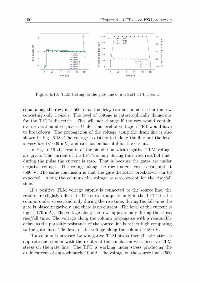
106 Chapter 6. TFT based ESD protection
0 20 40 60 80 100
-2
-1
0
1
2
TFT1 r1 c1 TFT2 r1 c2 TFT3 r1 c3 TFT4 r2 c1 TFT5 r2 c2 TFT6 r2 c3 TFT7 r3 c1 TFT8 r3 c2 TFT9 r3 c3
drai
n cu
rren
t [m
A]
time [ns]
0 20 40 60 80 100
0
100
200
300
400
500 V
G TFT1
VG TFT2
VG TFT3
voltage on the source line [V]vo
ltage
on
the
gate
line
[V]
time [ns]
-0.5
0.0
0.5
1.0
1.5
VS TFT7
VS TFT4
VS TFT1
Figure 6.18: TLM testing on the gate line of a α-Si:H TFT circuit.
equal along the row, it is 500 V, as the delay can not be noticed in the rowconsisting only 3 pixels. The level of voltage is catastrophically dangerousfor the TFT’s dielectric. This will not change if the row would containeven several hundred pixels. Under this level of voltage a TFT would haveto breakdown. The propagation of the voltage along the drain line is alsoshown in Fig. 6.18. The voltage is distributed along the line but the levelis very low (< 600 mV) and can not be harmful for the circuit.
In Fig. 6.19 the results of the simulation with negative TLM voltageare given. The current of the TFT’s is only during the stress rise/fall time,during the pulse the current is zero. That is because the gates are undernegative voltage. The voltage along the row under stress is constant at-500 V. The same conclusion is that the gate dielectric breakdown can beexpected. Along the columns the voltage is zero, except for the rise/falltime.
If a positive TLM voltage supply is connected to the source line, theresults are slightly different. The current appears only in the TFT’s in thecolumn under stress, and only during the rise time, during the fall time thegate is biased negatively and there is no current. The level of the current ishigh (-170 mA). The voltage along the rows appears only during the stressrise/fall time. The voltage along the column propagates with a reasonabledelay, as the parasitic resistance of the source line is rather high comparingto the gate lines. The level of the voltage along the column is 500 V.
If a column is stressed by a negative TLM stress then the situation isopposite and similar with the results of the simulation with positive TLMstress on the gate line. The TFT is working under stress producing thedrain current of approximately 10 mA. The voltage on the source line is 500
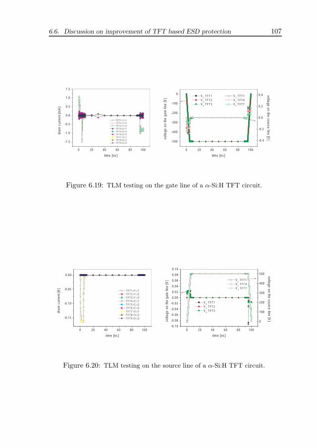
6.6. Discussion on improvement of TFT based ESD protection 107
0 20 40 60 80 100
-1.5
-1.0
-0.5
0.0
0.5
1.0
1.5
TFT1 r1 c1 TFT2 r1 c2 TFT3 r1 c3 TFT4 r2 c1 TFT5 r2 c2 TFT6 r2 c3 TFT7 r3 c1 TFT8 r3 c2 TFT9 r3 c3
drai
n cu
rren
t [m
A]
time [ns]
0 20 40 60 80 100
-500
-400
-300
-200
-100
0 V
G TFT1
VG TFT2
VG TFT3
volta
ge o
n th
e ga
te li
ne [V
]
time [ns]
-0.4
-0.2
0.0
0.2
0.4 VS TFT1
VS TFT4
VS TFT7
voltage on the source line [V]
Figure 6.19: TLM testing on the gate line of a α-Si:H TFT circuit.
0 20 40 60 80 100
-0.15
-0.10
-0.05
0.00
TFT1 r1 c1 TFT2 r1 c2 TFT3 r1 c3 TFT4 r2 c1 TFT5 r2 c2 TFT6 r2 c3 TFT7 r3 c1 TFT8 r3 c2 TFT9 r3 c3
drai
n cu
rren
t [A
]
time [ns]
0 20 40 60 80 100-0.10
-0.08
-0.06
-0.04
-0.02
0.00
0.02
0.04
0.06
0.08
0.10
VG TFT1
VG TFT2
VG TFT3
volta
ge o
n th
e ga
te li
ne [V
]
time [ns]
0
100
200
300
400
500
VS TFT1
VS TFT4
VS TFT7
voltage on the source line [V]
Figure 6.20: TLM testing on the source line of a α-Si:H TFT circuit.

108 Chapter 6. TFT based ESD protection
0 20 40 60 80 100-0.18
-0.16
-0.14
-0.12
-0.10
-0.08
-0.06
-0.04
-0.02
0.00
0.02
TFT1 r1 c1 TFT2 r1 c2 TFT3 r1 c3 TFT4 r2 c1 TFT5 r2 c2 TFT6 r2 c3 TFT7 r3 c1 TFT8 r3 c2 TFT9 r3 c3
drai
n cu
rren
t [A
]
time [ns]
0 20 40 60 80 100-0.1
0.0
0.1
0.2
0.3
0.4
0.5
VG TFT1
VG TFT2
VG TFT3
voltage on the source line [V]
volta
ge o
n th
e ga
te li
ne [V
]
time [ns]
-500
-400
-300
-200
-100
0 VS TFT7
VS TFT4
VS TFT1
Figure 6.21: TLM testing (negative voltage) on the source line of a α-Si:H TFTcircuit.
0 20 40 60
-0.7
-0.6
-0.5
-0.4
-0.3
-0.2
-0.1
0.0
0.1
drai
n cu
rren
t [A
]
time [ns]
TFT1 r1 c1 TFT2 r1 c2 TFT3 r1 c3 TFT4 r2 c1 TFT5 r2 c2 TFT6 r2 c3 TFT7 r3 c1 TFT8 r3 c2 TFT9 r3 c3
-10 0 10 20 30 40 50 60 70 80
0
500
1000
1500
2000 voltage on the source line [V]vo
ltage
on
the
gate
line
[V]
time [s]
VG TFT1
VG TFT2
VG TFT3
-10
0
10
20
30
40
50
VS TFT7
VS TFT4
VS TFT1
Figure 6.22: HBM testing on the gate line of a α-Si:H TFT circuit.
V.If HBM stress is supplied to the gate line, through a capacitor of 100 pF
pre-charged with 2×10⁻⁷ C (2 kV) and a resistor of 1500 Ω then a situationas presented in Fig. 6.22 happens. Full discharge of the HBM capacitor isnot possible as there is no current path to the ground in the circuit. Thevoltage is redistributed and the voltage on the gate line is almost equal to2000 kV, as the equivalent capacitance of the matrix is very small comperingwith 100 pF HBM capacitance. The peak current through TFT’s is -155mA.
If the HBM capacitor is connected to the source line, the decay timeis longer, as the source line has a larger resistance, as shown in Fig. 6.23.The peak current in the TFT’s is also higher (-600 mA) and the voltage

6.6. Discussion on improvement of TFT based ESD protection 109
0 20 40 60 80 100
-0.8
-0.6
-0.4
-0.2
0.0
TFT1 r1 c1 TFT2 r1 c2 TFT3 r1 c3 TFT4 r2 c1 TFT5 r2 c2 TFT6 r2 c3 TFT7 r3 c1 TFT8 r3 c2 TFT9 r3 c3
drai
n cu
rren
t [A
]
time [ns]
0 20 40 60 80 100-0.1
0.0
0.1
0.2
0.3
0.4
0.5
voltage on the source line [V]
VG TFT1
VG TFT2
VG TFT3
volta
ge o
n th
e ga
te li
ne [V
]
time [ns]
0
500
1000
1500
2000
VS TFT7
VS TFT4
VS TFT1
Figure 6.23: HBM testing on the source line of a α-Si:H TFT circuit.
0 20 40 60 80 100
-4
-2
0
2
4
TFT1 r1 c1 TFT2 r1 c2 TFT3 r1 c3 TFT4 r2 c1 TFT5 r2 c2 TFT6 r2 c3 TFT7 r3 c1 TFT8 r3 c2 TFT9 r3 c3
drai
n cu
rren
t [m
A]
time [ns]
0 20 40 60 80 100-100
0
100
200
300
400
500 V
G TFT1
VG TFT2
VG TFT3
volta
ge o
n th
e ga
te li
ne [V
]
time [ns]
-4
-2
0
2
4 voltage on the source line [V]
VS TFT1
VS TFT4
VS TFT7
Figure 6.24: MM testing on the gate line of a α-Si:H TFT circuit.
distribution is slightly different. The voltages along the stressed source lineare 1900 V. If the Machine model (MM) is used to test the gate line, thedistribution of the currents and voltages in the circuit is as shown in Fig.6.24. In the MM a capacitor of 200 pF is charged up to 200 V and through ainductor of 7.5 µH is discharged to the circuit. The voltage on the stressedline rises up to 400 V, which is above the breakdown voltage. Clearly someprotection is needed.
Simulations with protection elements
Finally a simulation of the LCD with the protection as used in the testedsamples is given. The chosen type of protection is “Double TFT, doublesided, single ring”. The results of the simulation with a positive TLM stress

110 Chapter 6. TFT based ESD protection
VTLM
pixel
Rline Lline R /2gl L /2gl R /2glL /2gl
Cco
Cds
Clc
Cst
Ccoup
Ldl
Rdl
TFT
Rprot
Figure 6.25: Schematic representation of ESD protection structure.
on the gate line are repeated on the circuit with ESD protection. The resultsare compared with Fig. 6.18 and they are completely the same. Apparentlythe protection element does not have any impact on the circuit responseunder an ESD stress. The TFT’s in the ESD protection structure do switchon under the ESD stress, and they conduct certain level of current. Thiscurrent has not any effect on the final voltage on the line. The resistance ofthe line is too low to produce sufficient voltage drop along the line.
The conclusion from these simulations is that the most important issuewhen designing an ESD protection in TFT LCD’s is to find way to reducethe voltage along the stresses gate/source line, as this is the most dangerousissue that appears during an ESD event in AMLCD’s. A resistor has to beintroduced along with the TFT chain in the way as shown in Fig. 6.25.
A simulation of TLM stress with ESD protection as in Fig. 6.25 is shownin Fig. 6.26. The value of resistor Rprot is chosen at 200 Ω. In Fig. 6.26both the stress voltage of TLM voltage generator and the voltages alongthe row under stress are shown. It is clear that the voltages on the TFT’sgates are dropped down to 150 V, which is under the edge of breakdown.In this way the TFT’s are fully protected from the TLM stress of 500 V.In order to protect the circuit from a higher voltage, the value of resistanceRprot should have been enlarged.
Unfortunately the drawback of this protection is that the leakage cur-rents of the protection TFT’s would cause a drop of the voltage along the lineduring the normal operation too, and a leakage current itself is detrimen-tal in battery operated equipments (displays in mobile phones are alwayson, even in the standby mode). For example, if the leakage current of thechain is 0.01 mA (thinking of 1000 rows/columns each with a protection

6.6. Discussion on improvement of TFT based ESD protection 111
0 20 40 60 80 100
0
100
200
300
400
500
VG(TFT1, TFT2, TFT3)
VTLM
volta
ge o
n th
e ga
te li
ne [V
]
time [ns]
Figure 6.26: Voltage propagation along the stressed gate line with Rprot = 200Ωand VTLM = 500V .
TFT chain), we can expect to see a voltage drop of ∆V = 200Ω · 0.01 mA=2 mV. In some applications, like automotive or TV/computer screen, thatdoes not give problems, but in the mobile phones that could be a strongdisadvantage.
If HBM stress is supplied, the TFT chain offers in this case quite enoughESD protection, as the resistance of the human body model itself (1500Ω) is enough to suppress the voltage along the line. If the human bodycapacitor is charged up to 2 kV, then the voltage on the TFT’s gates in thestressed row has its peak at 60 V. The resistor Rprot = 200 V in series withRHBM = 1500 kV has only marginal influence. It has to be noted here thatthe simulated TFT’s have an increased electron mobility and therefore theyconduct a much larger current then the real α-Si:H TFT’s.
If we consider Machine Model (MM), simulating handling by equipment(robots, testers, transportation equipment), as explained earlier in 2.1.1,then the situation is again similar with the TLM. The resistance of the MMis zero, but there is 0.75 µH inductor in series, and the resistance Rprot isneeded to provide the voltage drop. The voltage distribution along the rowunder MM stress with the protection chains and the protection resistor isshown in Fig. 6.27. If the value of 200Ω is chosen for Rprot, the circuitwould be able to withstand the MM stress of 200 V, which is standard forthis test, and even much higher MM stress.

112 Chapter 6. TFT based ESD protection
0 100 200 300 400 500 600
0
50
100
150
200
VG(TFT1, TFT2, TFT3)
V(CMM
)
volta
ge o
n th
e ga
te li
ne [V
]
time [ns]
Figure 6.27: Voltage propagation along the stressed gate line with Rprot = 200Ωand VMM = 200V .
These simulations are providing a good explanation of the real ESDevent, but still, many parameters are only approximated and can not beused directly for the ESD design. For example, the ESD protection ofthe displays tested in Section 6.3.2 conduct a current of only 0.02 A whenstresses by 300 V TLM stress. If we assume that HBM stress is supplied,with 2kV HBM voltage. To provide a voltage drop of 1.7 kV, (so thatthe circuit would be supplied with 300 V, which is bellow the breakdownvoltage and would produce the current of 0.02 A) we need a resistor ofR = 1700V/0.02A = 85kΩ and may influence the proper operation of thematrix although the matrix gives only capacitive loading. This is a quitelarge resistor and it would be difficult for realisation. The best way isto increase the current of the TFT chain by factor 10, using the TFT inthe chain with W/L ration 10 times larger then currently used, and theprotection resistor of 8.5 kΩ. This resistor would be easily realised withITO transparent metallisation layer, which has a very large sheet resistance(500 Ω
sq ).It is obvious that the design of ESD protection has to satisfy many
requirements to be efficient under different ESD tests. The solution thatwill respond satisfactory well under all ESD tests would be ideal. Among allpossible solutions one that would give the best response under the test whichis the most adequate for a specific application would be the favourite. It is
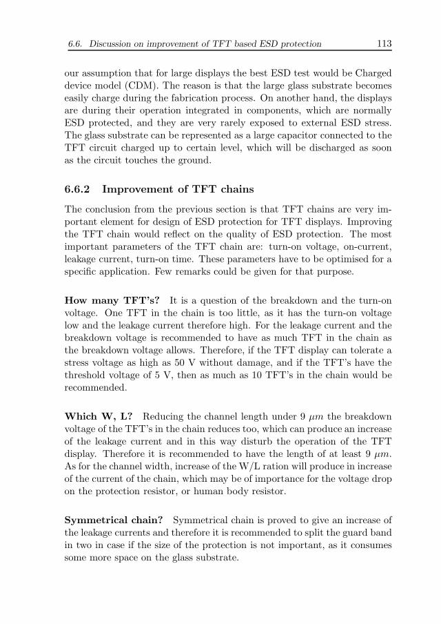
6.6. Discussion on improvement of TFT based ESD protection 113
our assumption that for large displays the best ESD test would be Chargeddevice model (CDM). The reason is that the large glass substrate becomeseasily charge during the fabrication process. On another hand, the displaysare during their operation integrated in components, which are normallyESD protected, and they are very rarely exposed to external ESD stress.The glass substrate can be represented as a large capacitor connected to theTFT circuit charged up to certain level, which will be discharged as soonas the circuit touches the ground.
6.6.2 Improvement of TFT chains
The conclusion from the previous section is that TFT chains are very im-portant element for design of ESD protection for TFT displays. Improvingthe TFT chain would reflect on the quality of ESD protection. The mostimportant parameters of the TFT chain are: turn-on voltage, on-current,leakage current, turn-on time. These parameters have to be optimised for aspecific application. Few remarks could be given for that purpose.
How many TFT’s? It is a question of the breakdown and the turn-onvoltage. One TFT in the chain is too little, as it has the turn-on voltagelow and the leakage current therefore high. For the leakage current and thebreakdown voltage is recommended to have as much TFT in the chain asthe breakdown voltage allows. Therefore, if the TFT display can tolerate astress voltage as high as 50 V without damage, and if the TFT’s have thethreshold voltage of 5 V, then as much as 10 TFT’s in the chain would berecommended.
Which W, L? Reducing the channel length under 9 µm the breakdownvoltage of the TFT’s in the chain reduces too, which can produce an increaseof the leakage current and in this way disturb the operation of the TFTdisplay. Therefore it is recommended to have the length of at least 9 µm.As for the channel width, increase of the W/L ration will produce in increaseof the current of the chain, which may be of importance for the voltage dropon the protection resistor, or human body resistor.
Symmetrical chain? Symmetrical chain is proved to give an increase ofthe leakage currents and therefore it is recommended to split the guard bandin two in case if the size of the protection is not important, as it consumessome more space on the glass substrate.
114 Chapter 6. TFT based ESD protection
6.7 Summary
As a first step to the development of design guidelines for ESD protectionof TFT LCD’s, the sensitivity of TFT LCD’s with four different protec-tion structures was investigated by means of a TLM tester. The resultsshowed that the four different ESD protection structures did not produceany difference in TLM sensitivity of TFT LCD’s. Therefore, testing wascontinued by testing the ESD protection structures only, isolated from theTFT LCD’s. The four ESD protection structures showed variations of theTLM breakdown voltage, which were in all cases lower then the previouslymeasured TLM breakdown voltage of the TFT LCD’s. It was concludedthat the ESD protection do not have impact on the TLM response of thedisplays. The only effect of a broken ESD protection could have been de-tected in the TLM curve of the display as a very small increase of the TLMcurrent.
To find out why different ESD protections do not produce difference inthe displays TLM sensitivity, a TFT LCD display has been modelled andsimulated by means of a circuit simulator. The TFT LCD has been simu-lated with and without ESD protection structure, and on HBM, MM andTLM stress. The circuit parameters used in the model have been estimatedfor an imaginary TFT LCD. Therefore there is a difference between themeasured and simulated ESD sensitivity levels. Still, the simulation helpsto explain the behaviour of the tested displays under the TLM stress. Itwas found that the ESD protection structure based on a TFT chain only,as in the tested TFT LCD’s, does not act as a protection under ESD stress.The structure has to be improved introducing a resistor in series to the dataline, which would be large enough to provide a sufficient voltage drop, suchthat the voltage on the line never exceeds 300 V.
Finally, it was analysed how a protection structure can be optimised, insense of an improved TFT chain in series with an optimised resistor.

Chapter 7
Summary andrecommendations
7.1 Summary
Although amorphous silicon thin film transistors (α-Si:H TFT’s) have avery low electron mobility and pronounced instabilities of their electricalcharacteristics, they are still very useful and they have found their placein the semiconductors industry, as they possess some very good properties:they can be deposited under low temperature and over a large area, and theyare very cheap. It is proved from practice that electrostatic discharge (ESD)is one of the most important issues in thin film electronics. It jeopardisesreliable operation of thin film transistors, firstly during the manufacturingprocess in the cleanroom, and also in some cases during their operation.Having a large on-resistance, α-Si:H TFT’s are very difficult from the pointof ESD protection, as it is difficult to sink the current. Another difficultyfor the ESD protection is that they are also built on an insulation substrate.Finally, the testing methods and the design rules that are already developedfor the silicon integrated circuits are not applicable on the amorphous siliconTFT’s. Therefore an original design has to be created in order to protectTFT circuits from the electrostatic discharge.
This work addresses the study of electrostatic discharge stressing in thinfilm transistors. Therefore, coupled gate α-Si:H TFT’s have been exposedto various experiments with ESD, in order to analyse their behaviour un-der ESD stress. It was established that “soft” degradation appears priorto breakdown. This soft degradations is visible through a threshold voltageshift (decrease). This consequently implies a leakage current increase. This
115

116 Chapter 7. Summary and recommendations
degradation is due to ESD stress created states in the amorphous siliconband gap. It was also shown that the breakdown voltage is linearly depen-dent on the channel length in short-channel TFT’s, and that it is constantfor the channel lengths longer then 9 µm. Breakdown in long TFT’s is due toa high electric field in the gate insulator. In the short TFT’s punch-throughand avalanche breakdown occurs.
Self-heating in the TFT’s with different channel lengths and also underESD stress of different pulse duration has been simulated. It is provedthat short channel TFT’s suffer from the effect of self-heating, while in longchannel TFT’s that it is reduced. The time needed to reach a temperatureequilibrium in a TFT is around 15 µs. Pulses shorter then this (ESD pulses)will not induce as large effect of self-heating as the long (> 15µs) ones.
A good example is a fingerprint sensor which has to be able to deal withthe static charge accumulated in a human body. A sensor has been designand manufactured. The effect of ESD has been analysed.
Finally ESD stress in a real TFT circuit has been tested and evaluated.The general conclusions are:
• TFT’s in a grounded gate configuration do not show a useful snap-back regime. Catastrophic (thermal) breakdown of the gate dielectrichappens at dielectric breakdown voltages, which implicitly means thatfurther circuits are not protected.
• TFT’s used as diode in a chain have to be used in series with a re-sistance. Its function has to be optimised in order to decrease thevoltage in the circuit below 300 V. Therefore the TFT’s used in chainhave to be designed to conduct as large current as possible.
7.2 Recommendations for future research
There are plenty issues that need more attention designing ESD protectionstructures for AMLCD’s, or other TFT based devices. Design rules fromalready developed ESD protections in IC technolgy are often simply trans-lated in thin film technology. In practice, these ESD protections in thin filmtechnology, often based on only one, very simple and surely not satisfactoryESD protection device, a TFT/diode chain, does not provide sufficient levelof protection.
Testing of single TFT’s behaviour under ESD stress showed that TFT’swith a longer channel length have higher breakdown voltage. This prop-erty should be kept in mind when designing protection structures. ESD

7.2. Recommendations for future research 117
protections with optimised TFT’s should be manufactured and tested. Tofurther improve the breakdown voltage, special high voltage TFT’s with thedrain extension could be built. Increase of the channel length in protectionTFT’s must be followed with an increase of the channel width. To increasethe current by a larger W/L ratio, wide channel TFT’s should be used.
ESD protections in AMLCD’s has to be improved by means of a serialresistor and an improved TFT chain in parallel. It is recommended to makeinherent use of long lines for realisation of the serial resistor Rprot. A goodusage of ITO, high resistive metallisation layer, would help to increase theinput line resistance.
It is highly recommended to introduce ESD testing and ESD standardsin large area electronics. HBM and MM testing of displays should becamea standard procedure.
ESD testing by means of CDM instead of TLM measurements set-upwould be a very interesting experiment. First reason is that TLM set-up isvery difficult for ESD testing of TFT’s, as in some cases the TLM current istoo low to be measured. But also, CDM model could give a better emulationof reality in which TFT’s operate. This assumption is build on the fact thatAMLCD’s are very easily charged during the manufacturing process.

118 Chapter 7. Summary and recommendations

Bibliography
[1] A. Amerasekera, S. P. Kwok, and J. Seitchik. Current transport mod-elling in an amorphous silicon antifuse structure. In Proc. of MRSSymp., volume 297, pages 999–1004, 1993.
[2] H. Aoki. Dynamic characterization of a-si tft-lcd pixels. IEEE Trans.on Electron Devices, 43(1):31–39, 1996.
[3] N. Arora. MOSEFET Models for VLSI Circuit Simulation, Theory andPractice. Springer-Verlag, 1993.
[4] S. Bijlsma. Electrostatic damage in tfd-r displays. Technical report,University of Twente, 1996.
[5] S. J. Bijlsma, H. van Kranenburg, K. J. B. M. Nieuwesteeg, and M. G.Pitt. Electrical breakdown of amorphous hydrogenated silicon rich sil-icon nitride thin film diode. IEEE Transactions on Electron Devices,43(9):1592–1601, 1996.
[6] Niel Bird. Philips research laboratories. Personal communication.
[7] H. C. Cheng, J. W. Tsai, C. Y. Huang, F. C. Luo, and H. C. Tuan. Theinstability characteristics of amorphous silicon thin film transistors withvarious interfacial and bulk defect states. Japanese Journal of AppliedPhysics, 36(10):6226–6229, 1997.
[8] Y. Cheng and T. Fjeldly. Unified physical iv model of fully depletedsoi/mosfets for analog/digital circuit design. Solid State Electronics,39(5):720–730, 1996.
[9] C. Chiang, S. Martin, J. Kanicki, Y. Ugai, and T. Yukawa. Top-gate staggered amorphous silicon thin-film transistors: series resistanceand nitride thickness effects. Japanese Journal of Applied Physics,37(11):5914–5920, 1998.
119
120 Bibliography
[10] S. Dabral and T. Maloney. Basic ESD and I/O Design. Wiley, 1998.
[11] H. C. de Graaff and F. M. Klaassen. Compact Transistor Modelling forCircuit Design. Springer-Verlag, 1990.
[12] S. C. Deane and M. J. Powell. Field-effect conductance in amorphoussilicon thin-film transistors with a defect pool density of states. Journalof Applied Physics, 74(11):6655–6666, 1993.
[13] Steave Deane. Philips reserch laboratories.
[14] Device simulation software Silvaco International. SILVACO ATLASuser’s manual, 1997.
[15] V. M. Dwyer, A. J. Franklin, and D. S. Campbell. Thermal failure insemiconductor devices. Solid-State Electronics, 33:553–560, 1990.
[16] ESD Association Standard. ESD senitivity testing: Human Body Model(HBM) - Component level, 1993. S5.1.
[17] ESD Association Standard. ESD sensitivity testing: Machine Model(MM) - Component level, 1994. S5.2.
[18] ESD Association Standard. ESD Sensitivity Testing: Charged DeviceModel (CDM) - Component level, 1997. D5.3.
[19] M. J. Powell et al. A 6in full-colour liquid crystal television using anactive matrix of amorphous-silicon tfts. In Proc. SID, volume 29, pages227–232, 1988.
[20] T. Globus, B. Gelmont, R. J. Mattacuch, and L. Q. Sun. Defect density-of-states a-si:h tfts. In Proc. of Material Research Society Symposium,volume 420, pages 263–268, 1996.
[21] N. Tosic Golo, S. van der Wal, F. G. Kuper, and T. Mouthaan. Time-voltage trade-off for esd damage threshold in amorphous silicon thinfilm transistors. volume 41, pages 1391–1396, 2001.
[22] C. F. O. Graeff, M. S. Brandt, M. Stutzmann, and M. J. Powell. Defectcreation in amorphous-silicon thin-film transistors. Phusical Review B,52(7):4680–4683, 1995.
[23] A. S. Grove. Physics and technology of semiconductor devices. JohnWiley and Sons, 1967.

Bibliography 121
[24] M. Grunewald, P. Thomas, and D. Wurtz. A simple scheme for evalu-ating field effect data. Physica Status Solidi (b), 100:K139–K143, 1980.
[25] M. Hack, A. Chiang, T. Y. Huang, A. G. Lewis, R. A. Martin, H. Tuan,I. W. Wu, and P. Yap. High-voltage thin film transistors for largearea microelectronics. In Proc. of IEEE International Electron devicemeeting (IEDM), pages 252–255, 1988.
[26] M. Hack, M. Shur, and J. G. Shaw. Physics models for amorphous-silicon thin-film transistors and their implementation in a circuit sim-ulation program. IEEE Trans. on Electron Devices, 36(12):2764–2769,1989.
[27] J. R. Hwang, J. S. Park, M. C. Jun, J. Jang, and M. K. Han. Extrac-tion of altered localized-states in a-si and poly-si tft’s under variousconditions. In Proc. of Material Research Society Symposium, volume297, pages 913–918, 1993.
[28] Eran Ishay. Orboteche ltd. Personal communication.
[29] Y. Kaneko, A. Sasano, and T. Tsukada. Characterization of instabilityin amorhous silicon thin-film transistors. Journal of Applied Physics,69(10):7301–7305, 1991.
[30] J. Kanicki, editor. Amorphous and microcrystalline semiconductor de-vices, volume II. Artech House, 1992.
[31] C. H. Kim and M. Matsumura. Short-channel amorphous-silicon thin-film transistors. IEEE Trans. Electron Devices, 43(12):2172–2176,1996.
[32] Alan G. Knapp. Fingerprint sensing device and recognition systemhaving predetermined electrode activation, June 1994.
[33] F. R. Libsch and J. Kanicki. Bias-stress-induced streched-exponentialtime dependence of charge injection and trapping in amorphous thin-film transistors. Applied Physics Letters, 62(11):1286–1288, 1993.
[34] K. Machida, S. Shigematsu, H. Morima, N. Shimoyama, Y. Tanabe,T. Kumazaki, K. Kudou, M. Yano, and H. Kyuragi. A new sen-sor structure and fabrication process for a single-chip fingerprint sen-sor/identifier lsi. In Proc. of IEEE International Electron Devices Meet-ing (IEDM), pages 887–890, 1999.

122 Bibliography
[35] A. Madan and P. G. Le Comber. Field-effect in substitutionally dopeda-si films. In Proc. of the 7th International Conference on Amorphousand Liquid Semiconductors, pages 377–381, 1977.
[36] T. J. Maloney and N. Khurana. Transmission line pulsing techniquesfor circuit modelling of esd phenomena. In EOS/ESD Proc., pages49–54, 1985.
[37] G. Notermans. On the use of n-well resistors in esd protections. Mi-croelectronics Reliability, 38:1741–1748, 1998.
[38] M. Ohta, M. Tsumura, J. Ohida, J. Ohwada, and K. Suzuki. Activematrix network simulator considering nonlinear c-v characteristics oftft’s intrinsic capacitances. In Proc. of Japan Display Conf., pages431–434, 1992.
[39] F. Parrain, B. Charlot, N. Galy, and B. Courtois. A cmos compatibilemicromachined tactile fingerprint sensor. In Proc. of Design, Test,Integration and Packaging of MEMS/MOEMS.
[40] Philips ED&T/Analogue simulation. PSTAR Reference Manual, 1994.
[41] Michael Pitt. Philips mobile display systems. Personal communication.
[42] M. J. Powell. Analysis of field-effect-conductance measurements onamorphous semiconductors. Philosophical Magazine B, 43(1):93–103,1981.
[43] M. J. Powell. The physics of amorphous-silicon thin-film transistors.IEEE Trans. on Electron Devices, 36(12):2753–2763, 1989.
[44] M. J. Powell, C. van Berkel, and S. C. Deane. Instability mechanismsin amorphous silicon thin film transistors. Journal of Non-CrystallineSolids, 137-138:1215–1220, 1991.
[45] M. J. Powell, C. van Berkel, and J. R. Hughes. Time and temperaturedependence of instability mechanisms in amorphous silicon thin filmtransistors. Applied Physics Letters, 54(14):1323–1325, 1989.
[46] R. G. Renninger. Mechanism of charged-device electrostatic discharge.In Proc. of EOS/ESD Symp., page 127, 1991.
[47] N. Tosic S. van der Wal, F. Kuper, and T. Mouthaan. Time-dependantdegradation effects in top-gate amorphous silicon hydrigenated thin-film transistors. In Proc. of SAFE, pages 153–157, 2000.

Bibliography 123
[48] R. Schropp and M. Zeman. Amorphous and microcrystalline silicon so-lar cells: modelling, materials and device technology. Kluwer AcademicPublishers, 1998.
[49] R. E. I. Schropp and J. F. Verwey. Undoped amorphous silicon tftswith n-channel or p-channel device operation for the determinationof the gap states distribution. In Proc. of Material Research SocietySymposium, volume 95, pages 489–495, 1987.
[50] R. Schumacher, P. Thomas, K. Weber, W. Fuhs, F. Djamdji, P. G. LeComber, and R. E. I. Schropp. Temperature-dependent effects in field-effect measurements on hydrogenated amorphous silicon thin-film tran-sistors. Physica Status Solidi (b), 58(4):K139–K143, 1988.
[51] S. Shigematsu, H. Morimura, Y. Tanabe, T. Adachi, and K. Machida.A single-chip fingerprint sensor and identifier. IEEE Journal of solidstate circuits, 34(12):1852–1859, 1999.
[52] M. Shur, M. Hack, and J. G. Shaw. A new analytical model for amor-phous silicon thin-film transistors. J. of Applied Physics, 66(7):3371–3380, 1989.
[53] M. Shur, M. Hack, J. G. Shaw, and R. A. Martin. Capacitance-voltagecharacteristics of amorphous silicon thin-film transistors. J. of AppliedPhysics, 66(7):3381–3385, 1989.
[54] M. S. Shur, M. Hack, and C. Hyun. Flat-band voltage and surfacestates in amorphous silicon-based alloy field-effect transistors. Journalof Applied Physics, 56(2):382–386, 1984.
[55] M. S. Shur, H. C. Slade, T. Ytterdal, L. Wang, Z. Xu, M. Hack, K. Afla-tooni, Y. Byin, Y. Chen, M. Froggatt, A. Krishnan, P. Mei, H. Meiling,B. H. Min, A. Nathan, S. Sherman, M. Stewart, and S. Theiss. Model-ing and scaling of a-si:h and poly-si thin film transistors. In Mat. Res.Soc. Symp. Proc., volume 467, pages 831–842, 1997.
[56] H. C. Slade and M. S. Shur. Analysis of bias stress on unpassivatedhydrogenated amorphous silicon thin-film transistors. Transactions onElectron Devices, 45(7):1548–1553, 1998.
[57] W. E. Spear and LeComber. Solid state communications, 17:1193, 1975.
[58] R. A. Street. Hydrogen diffusion and electronic metastability in amor-phous siliscon. Physica B, pages 69–81, 1991.

124 Bibliography
[59] R. A. Street. Hydrogenated amorphous silicon. Cambridge UniversityPress, 1991.
[60] T. Suzuki, Y. Osaka, and M. Hirose. Theoretical interpretations ofthe gap state density determined from the field effect and capacitance-voltage characteristics of amorphous semiconductors. Japanese Journalof Applied Physics, 21(3):L159–L161, 1982.
[61] M. Tada, S. Uchikoga, and M. Ikeda. Power-density-dependant failureof amorphous si tft. In Proc. of AMLCD, pages 269–272, 1996.
[62] Y. H. Tai, J. W. Tsai, H. C. Cheng, and F. C. Su. Anomalous bias-stress-induced unstable phenomena of hydrogenated amorhous siliconthin-film transistors. Applied Physics Letters, 67(1):76–78, 1995.
[63] M. T. Thompson. Inductance calculation techniques - part ii: Ap-proximations and handbook methods. Power Control and IntelligentMotion, 25(12), 1999.
[64] N. Tosic, G. Boselli, H. van Kranenburg, F. Kuper, and T. Mouthaan.The behaviour of a-si:h thim film transistors during electrostatic dis-charge. In Proc. of SAFE, pages 545–548, 1998.
[65] N. Tosic, F. Kuper, and T. Mouthaan. Electrostatic discharge induceddegradation in top-gate amorphous silicon thin film transistors. InProc. of SAFE, pages 515–520, 1999.
[66] N. Tosic, F. Kuper, and T. Mouthaan. Degradation of a-si:h tft’s causedby electrostatic discharge. In Proc. of MIEL, pages 359–362, 2000.
[67] N. Tosic, F. Kuper, and T. Mouthaan. High voltage effects in top-gate amorphous silicon thin-film transistors. In Proc. of MRS, pagesQ8.5.1–Q8.5.6, 2000.
[68] N. Tosic, F. Kuper, and T. Mouthaan. Analysis of the electrical break-down in hydrogenated amorphous silicon thin-film transistors. IEEETransaction on Electron Devices, 49(6):1012–1018, 2002.
[69] N. Tosic, F. Kuper, T. Mouthaan, and S. van der Wal. Estimateof the impact of electrostatic discharge on density of states in hy-drogenated amorphous silicon thin film transistors. Applied PhysicsLetters, 80(18):3337–3339, 2002.

Bibliography 125
[70] N. Tosic, F. G. Kuper, and T. Mouthaan. Transmission line modeltesting of top-gate amorphous silicon thin film transistors. In Proc. ofIRPS, pages 289–294, 2000.
[71] T. Tsukada. TFT/LCD Liquid Crystal displays addressed by thin-filmtransistors. Gordon and Breach Science Publishers, 1996.
[72] Frank Werner. Bosch. Personal Communication.
[73] R. Woltjer, A. Hamada, and E. Takeda. Time dependence of p-mosfethot-carrier degradation measured and interpreted consistently over tenorders of magnitude. IEEE Trans. on Electron Devices, 40(2):392–401,1993.
[74] D. C. Wunsch and R. R. Bell. Determination of threshold failure levelsof semiconductor diodes and transistors due to pulse voltages. IEEETrans. on Nuclear Science, 15:244, 1968.

126 Bibliography

Samenvatting
Amorf-silicium dunne film transistoren worden nog steeds veel gebruikt inde halfgeleider industrie, ondanks dat deze devices een erg lage elektronenmobiliteit hebben en uitgesproken instabiel zijn voor wat betreft hun elek-trische eigenschappen. Er zijn nl. ook enkele goede eigenschappen: deposi-tie kan plaatsvinden onder lage temperaturen en over een groot oppervlak.Bovendien zijn ze erg goedkoop. Uit de praktijk komt naar voren dat elek-trostatische ontlading (electrostatic discharge, ESD) een van de belangrijk-ste problemen in de dunne film elektronica is. Het staat een betrouwbarewerking van dunne film transistoren in de weg; in de eerste plaats tijdenshet produktie proces in de cleanroom, maar in sommige gevallen ook tij-dens gebruik. Vanwege hun hoge weerstand zijn α-Si:H TFT’s moeilijk tebeschermen tegen ESD en het is moeilijk om de stroom omlaag te brengen.Een andere moeilijkheid van betreft ESD bescherming is het feit dat ze opeen isolerend substraat zijn gebouwd. Tot slot zijn de test methoden enontwerpregels die ontwikkeld waren voor de silicium geintegreerde circuitsniet bruikbaar voor α-Si TFT’s. Voor de bescherming van TFT circuitstegen ESD zal moeten worden omgezien naar een alternatief ontwerp vande devices.
Dit werk behelst de studie naar elektrostatische stress in dunne filmtransistoren. Hiertoe zijn gekoppelde gate α-Si:H TFT’s blootgesteld aandiverse experimenten met ESD om zodoende hun gedrag onder ESD stress teanalyseren. Vastgesteld is dat ”zachte” degradatie plaatsvindt voor break-down. Deze zachte degradatie is zichtbaar vanwege een verschuiving in dedrempelspanning (verlaging). Dit heeft een verhoging van de lekstroom totgevolg. Deze degradatie is te wijten aan door ESD stress gecreeerde statesin de amorphous silicon band gap. Tevens is aangetoond dat het breakdownspanning lineair afhankelijk is van de channel lengte in korte kanaal TFT’s,en dat deze spanning constant is voor kanaal lengtes groter dan 9 µm.Breakdown in lange TFT’s is te wijten aan een hoog elektrisch veld in degate isolator. In korte TFT’s vindt punch-through en avalanche breakdown
127

plaats.Zelfverwarming in de TFT’s met verschillende channel lengtes alsmede
onder ESD stress met verschillende pulsduur is gesimuleerd. Het is bewezendat korte kanaal TFT’s te lijden hebben onder zelfverwarming, terwijl dateffect gereduceerd is in lange kanaal TFT’s. De tijd die benodigd is om eentemperatuursevenwicht te bereiken bedraagt ongeveer 15 µs. Korte pulsen(ESD pulsen) wekken minder zelfverwarming op dan lange pulsen (¿15 µs).
Een goed voorbeeld is de vingerafdruk sensor, die bestand moet zijntegen de statische lading die is opgebouwd in het menselijk lichaam. Eendergelijke sensor is ontworpen en gebouwd. Het effect van ESD hierop isgeanalyseerd.
Tot slot is ESD stress in een werkelijk TFT circuit getest en geevalueerd.Uithet resultaat blijkt dat een weerstand aan de TFT kettting moet wordentoegevoegd voor een efficiente ESD protectie. Het ontwerp van de protectiedient te worden geoptimaliseerd om de spanning in het circuit te verlagentot 300 V. Dit betekent, dat de TFT’s in the ketting een zo groot mogelijkestroom moeten kunnen voeren.
128
Author’s publications
1. N. Tosic, F. G. Kuper, T. Mouthaan, ”Degradation of a-Si:H TFTscaused by Electrostatic Discharge”, MIEL’00, 14-17 May, Nis, Yu-goslavia, pp. 359-362.
2. N. Tosic, F. G. Kuper, T. Mouthaan, ”Transmission Line ModelTesting of Top-Gate Amorphous Silicon Thin Film Transistors”, IRPS2000, 10-14 Apr. 2000, San Jose, CA, pp. 289-294.
3. N. Tosic, F. G. Kuper, T. Mouthaan, ”High voltage effect in top gateamorphous silicon thin film transistors”, MRS 2000 Spring Meeting,24-28 Apr. 2000, San Francisco, CA, MRS Proceedings Vol. 621, pp.Q8.5.1-Q.8.5.6.
4. N. Tosic Golo, S. van der Wal, F. G. Kuper, T. Mouthaan, ”Time-voltage trade-off for ESD damage threshold in amorphous silicon thinfilm transistors”, Microelectronics Reliability, Vol. 41 (2001) pp. 1391-1396, after ESREF 2001, 1-5 Oct. 2001, Arcachon, France.
5. N. Tosic Golo, F. G. Kuper, T. Mouthaan, ”Analysis of the electicalbreakdown in amorphous silicon thin-film transistors”, IEEE Trans-actions on Electron Devices, Vol. 49, No. 6 (2002) pp. 1012-1018.
6. N. Tosic Golo, S. van der Wal, F. G. Kuper, T. Mouthaan, ”Estima-tion of the impact of electrostatic discharge on density of states in hy-drogenated amorphous silicon thin-film transistors”, Applied PhysicsLetters, Vol. 80, No. 18 (2002) pp. 3337-3339.
7. N. Tosic Golo, F. G. Kuper, T. Mouthaan, ”Zapping Thin FilmTransistors”, Microelectronics Reliability Vol. 42 (2002) pp. 747-765.
8. N. Tosic Golo, F. G. Kuper, T. Mouthaan, M. Pitt, “Electrostaticdischarge protection in a-Si TFT circuits”, TFT Technology Sympo-sium VI, to be presented.
129

9. N. Tosic, G. Boselli, H. van Kranenburg, F. Kuper, T. Mouthaan,”The Behaviour of a-Si:H Thin Film Transistors During ElectrostaticDischarge”, poster, SAFE’98, 25-26 Nov. 1998, Mierlo, The Nether-lands, pp. 545-548.
10. N. Tosic, F. Kuper, T. Mouthaan, ”Electrostatic Discharge InducedDegradation in Top Gate Amorphous Silicon Thin Film Transistor”, poster, SAFE’99, 25-26 Nov. 1999, Mierlo, The Netherlands, pp.515-520.
11. S. van der Wal, N. Tosic, F. G. Kuper, T. Mouthaan, ” Time-dependent Degradation Effects in Top-gate Amorphous Silicon Hy-drogenated Thin-film Transistors”, poster, SAFE’00, 29 Nov. - 1 Dec.2000, Veldhoven, The Netherlands, pp. 153-158.
12. N. Tosic Golo, S. van der Wal, F. G. Kuper, T. Mouthaan, ”Es-timate of the impact of ESD stress on DOS in a-Si:H TFT’s”, oralpresentation at SID: Spring 2001 Meeting of Mid-European Chapter,5-6 Apr. 2001, Delft, The Netherlands.
13. N. Tosic Golo, T. Jenneboer, T. Mouthaan “Capacitive fingerprintsensor in amorphous silicon thin film technology”, poster, SAFE’02,to be presented.
130

Index
Aactivation energy, 21, 47AMLCD, 1amorphous silicon, 2avalanche multiplication, 35
Bband-gap density of states (DOS),
63field method calculation, 64deep states, 63tail states, 63
breakdown location, 40breakdown of the glass substrate,
42breakdown voltage
TFT chain, 96under TLM pulse, 16versus channel length, 17
Ccapacitance-voltage (C(V)) measure-
ments, 25Charged Device Model (CDM), 12critical electric field, 40
DDrain Induced Barrier Lowering (DIBL)
effect, 35
Eelectro-thermal simulations, 46electron mobility, 22
Electrostatic discharge (ESD), 11ESD protection, 85
Ffailure mode, 41fingerprint sensor, 71
capacitive principle, 72resistive principle, 83
flat band voltage, 67
Ggate dielectric breakdown, 41generation rate, 38grounded gate NMOS, 14
Hheat capacitance, 52heat flow equation, 51holding voltage, 14Human Body Model (HBM), 12
Iinterface charges, 22interface states
density, 24
MMachine Model (MM), 12
Pparasitic capacitances, 25PECVD, 2punch-through, 35
131
Sself-heating, 45snapback, 14subthreshold slope, 21
TTFTLCD, 85
gate delay, 102parasitics, 102storage capacitor, 99
thermal annealing, 28thermal modelling, 45thermal resistance, 52thin film transistor (TFT), 1
bottom gate, 4chain, 82coupled gate TFT, 82grounded gate TFT, 16high voltage TFT, 82long channel, 17short channel, 17top gate, 4
threshold of degradation, 20threshold voltage (VT ), 21
shift, 34turnaround phenomenon, 23
transconductance, 23Transmission Line Model (TLM),
13
WWunsch and Bell model, 33
132