Novel small-size directional antenna for UWB WBAN/WPAN applications
Hindawi Publishing CorporationInternational Journal of Microwave Science and TechnologyVolume 2010, Article ID 671515, 9 pagesdoi:10.1155/2010/671515
Research Article
New Design Method of UWB Microstrip Filters UsingAdaptive Genetic Algorithms with Defected Ground Structures
Amir Reza Dastkhosh,1 Gholamreza Dadashzadeh,2 and Mohammad Hossein Sedaaghi1
1 Faculty of Electrical Engineering, Sahand University of Technology, P.O. Box 51335-1996, Tabriz, Iran2 Faculty of Electrical Engineering, Shahed University, Tehran 3319118651, Iran
Correspondence should be addressed to Amir Reza Dastkhosh, amir reza [email protected]
Received 9 August 2009; Revised 5 January 2010; Accepted 6 March 2010
Academic Editor: Safieddin Safavi-Naeini
Copyright © 2010 Amir Reza Dastkhosh et al. This is an open access article distributed under the Creative Commons AttributionLicense, which permits unrestricted use, distribution, and reproduction in any medium, provided the original work is properlycited.
The effects of adaptive genetic algorithms (AGAs) and defected ground structures (DGSs) on performance optimization of taperedmicrostrip filter are investigated. The proposed structure achieves an ultra wide stopband with high attenuation within a smallsurface area, as well as 45% smaller size, in comparison with conventional filters. The parameters of the filter are optimized usingin-home AGA code. In the proposed AGA algorithm, the crossover and mutation probabilities are adaptively changed accordingto the value of individual fitness. Then by utilizing the proposed DGS, a compact S-band lowpass filter with ultra-wide spuriousfree window is obtained. The proposed filter achieves an insertion loss of 0.8 dB from DC up to 4 GHz and 21 dB rejection in thestopband from 4.3 up to 60 GHz. The fabricated and measured results exhibit good agreement with the simulated results. Theydemonstrate that combining AGA and DGS yields best possible response for this group of filters.
1. Introduction
In practice, high-performance microwave filters with min-imized size and weight are playing an important rolefor design and fabrication of high-efficiency miniaturizedmicrowave systems. Recently, due to high demand for broadband services, design of such miniaturized wide and ultra-wide stopband filters for interference cancellation (by meansof out of-band signal suppression) is gaining more and moreattention [1–4]. Nonuniform transmission lines (NUTLs)play an important role in microwave circuits. Applicationsinclude impedance transformation and matching, filters, anddirectional couples. The nonuniform line is traditionallyanalyzed in the frequency domain [5–7].
Genetic algorithms are widely employed in variousfields such as optimal engineering designs. They have beensuccessfully applied to finding the global optimum in avariety of unimodal domains. Parameter control methodsare classified as deterministic and adaptive. Deterministicsystems employ fixed, predefined parameters for GA. On theother hand, adaptive control uses feedback from the searchprocess to find out how the parameter values change [8, 9].
Many researchers have proposed and demonstratedelectromagnetic bandgap (EBG) microstrip structures toachieve compact and wide frequency stopband [10–12]. Alsorecently, DGSs have become one of the most interesting areasof research in modern communication systems [13–16]. TheDGS was first proposed by Kim et al. [17]. The microstripline with DGS patterns in the ground plane has the stopbandcharacteristics due to the equivalent effective inductance ofDGS. It modifies the characteristics of the transmission linesuch as line capacitance and inductance.
However none of these papers presents a combinedrigorous method to fully design and optimize new filters.We emphasize the new idea of optimization, analysis, andsynthesis on nonuniform transmission lines using adaptivegenetic algorithms and DGSs design methods. In sum, byusing adaptive genetic algorithms and DGSs, characteristicsand size of a tapered microstrip filter can be optimized. Thenew method yields a microstrip filter with high rejection inthe stopband and sharp transition with reduced insertionloss in passband. These features can be used in filter appli-cations to eliminate unwanted frequencies and to reduce thephysical size of a microstrip circuit. Conventional filtering
2 International Journal of Microwave Science and Technology
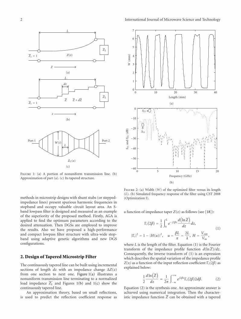
L
Zc = 1
Z
Z(z)
ZL
(a)
Zc = 1Z Z + dZ
ZL
dz
z
L
(b)
Port 1 Port 2W(i)
L
ZC(x)
(c)
Figure 1: (a) A portion of nonuniform transmission line. (b)Approximation of part (a). (c) Its tapered structure.
methods in microstrip designs with shunt stubs (or stepped-impedance lines) present spurious harmonic frequencies instopband and occupy valuable circuit layout area. An S-band lowpass filter is designed and measured as an exampleof the superiority of the proposed method. Firstly, AGA isapplied to find the optimum parameters according to thedesired attenuation. Then DGSs are employed to improvethe results. Also we have proposed a high-performanceand compact lowpass filter structure with ultra-wide stop-band using adaptive genetic algorithms and new DGSconfigurations.
2. Design of Tapered Microstrip Filter
The continuously tapered line can be built using incrementalsections of length dz with an impedance change ΔZ(z)from one section to next one. Figure 1(a) illustrates anonuniform transmission line terminating to a normalizedload impedance ZL and Figures 1(b) and 1(c) show thecontinuously tapered line.
An approximation theory, based on small reflections,is used to predict the reflection coefficient response as
0 10 20 30 400
1
2
3
4
5
6
7
W(m
m)
Length (mm)
(a)
0 5 10 15 20−60
−50
−40
−30
−20
−10
0
S 11
andS 2
1(d
B)
Frequency (GHz)
S11
S21
(b)
Figure 2: (a) Width (W) of the optimized filter versus its length(L). (b) Simulated frequency response of the filter using CST 2008(Optimization I).
a function of impedance taper Z(z) as follows (see [18]):
Γi(2β) = 1
2
∫ L
0e− j2βz
d(
lnZ)
dzdz,
|Γi|2 = 1− |H(u)|2, u = βL
π= 2L
λ, H = Vout
Vin,
(1)
where L is the length of the filter. Equation (1) is the Fouriertransform of the impedance profile function d(lnZ)/dz.Consequently, the inverse transform of (1) is an expressionwhich describes the spatial variation of the impedance profileZ(x) as a function of the input reflection coefficient Γi(2β) asexplained below:
12
d ln(Z)
dz= 1
2π
∫ +∞
−∞e j2βzΓi
(2β)2dβ. (2)
Equation (2) is the synthesis one. An approximate answer isachieved using numerical integration. Then the character-istic impedance function Z can be obtained with a tapered

International Journal of Microwave Science and Technology 3
0 10 20 30 400
1
2
3
4
5
6
W
Length (mm)
(a)
0 5 10 15 20−60
−50
−40
−30
−20
−10
0
S 11
andS 2
1(d
B)
Frequency (GHz)
S21
S11
(b)
Figure 3: (a) Width (W) of the optimized filter versus its length (L). (b) Simulated frequency response of the filter using Ansoft Designer 4(Optimization II).
microstrip filter as a primary structure. A lossless nonuni-form transmission line may be considered as a limitingcase where the number of nonuniform transmission lines(N) in stepped impedance transformers becomes infinitelylarge and, at the same time, the maximum length of eachnonuniform transmission line-section approaches to zero,provided that the total length L of the stepped impedancetransformer is equal to nonuniform transmission line. Toanalyze the filter, its structure is divided into a number ofshort segments based on the length of the filter as illustratedin Figure 1. The structure can be simulated more preciselyusing tapered sections. Therefore, the tapered sections areused for filter modeling [19, 20].
3. Adaptive Genetic Algorithms
In this section the optimization of the filter specificationsusing adaptive genetic algorithms [21–23] is introduced.The behavior of genetic algorithms is strongly influencedby the balance between exploration and exploitation. TheGA control parameter settings, such as mutation andcrossover probabilities (denoted by Pm and Pc, resp.) andthe population size, are key factors in the determinationof the exploitation versus exploration tradeoff. If poorsettings are used, the exploration/exploitation balance maynot be reached in a profitable way; the GA performanceis severely affected due to the possibility of prematureconvergence. Finding robust control parameters is not atrivial task since their interaction with GA performance isa complex relationship and the optimal ones are problemdependent. Therefore, adaptive GAs are considered wherethey dynamically adjust the selected control parameters orgenetic operators during the course of evolving a problemsolution. The significance of Pc and Pm in controlling GAperformance has been acknowledged in GA research [24–26].
Pc controls the rate at which a solution is subjected tocrossover. The higher the value of Pc, the quicker the newsolutions are introduced into the population. However, as Pcincreases, solutions can be disrupted faster than the selectioncan exploit them. Typical values of Pc are in the range 0.5–1.0. Mutation is another operator to restore genetic material.Larger values of Pm transform GA into a purely randomsearch algorithm while a little mutation is only requiredto prevent the premature convergence of the GA into asuboptimal solution. A good selection of Pc and Pm can leadto an easier search for good solution. Pm and Pc depend onthe fitness of the solutions and are zero for the solution withthe maximum fitness. Therefore, they are adapted as follows:
Pc = k1fMax − f ′
fMax − f(
if f ′ ≤ f =⇒ Pc = k3, k1 = k3 = 1)
,
Pm = k2fMax − f
fMax − f(
if f ≤ f =⇒ Pm = k4, k2 = k4 = 0.5).
(3)
f , fMax, f , and f ′ are the average fitness value of thepopulation, the maximum of the fitness, the fitness of eachmember of the population, and the larger fitness of thesolutions to be crossed, respectively. Also the normalizedfitness function is selected as
F = 100×(
23|S11| +
13|S21|
), (4)
where S11 and S21 are the worst points in the stopband andpassband regions, respectively.
As the signal’s frequency applied to millimeter-waveintegrated circuit is steadily increased, some characteristic

4 International Journal of Microwave Science and Technology
Microstrip line printedon the reverse side
of the substrate
1.9 mm(50 Ohm)
1.9 mm(50 Ohm)
R1
D1
D2 D3
(a)
(b)
D1R2
R3
R1
D2
D3
D7
D6
D4 D5
D8
PORTP = 1Z = 50 Ohm
PLCID = LC1
L = L0 nHC = C0 μF
PLCID = LC3
L = L2 nHC = C2 μF
PLCID = LC5
L = L4 nHC = C4 μF
PLCID = LC7
L = L6 nHC = C6 μF
PORTP = 2Z = 50 Ohm
SLCID = LC2
L = L1 nHC = C1 μF
SLCID = LC4
L = L3 nHC = C3 μF
SLCID = LC6
L = L5 nHC = C5 μF
SLCID = LC8
L = L7 nHC = C7 μF
(c)
Figure 4: Required DGS structures. (a) and (b) DGS (1) & DGS (2). (c) Resulting circuit model. Solid lines indicate that the slots are etchedin the ground plane of the microstrip.
5 10 15 20 25 30−50
−40
−30
−20
−10
0
DGS2 (Case A)DGS1 (Case A)DGS1 (Case B)
S 21
(dB
)
Frequency (GHz)
Figure 5: Frequency responses of DGS structures.
frequency may be reached at which undesirable effects occur.The same is true for monolithic integrated circuits. For asufficiently wide microstrip line, a transverse-resonant modeexists which can also be coupled strongly to the quasi-TEM microstrip mode. Therefore, because of fabricationtechnology and in order to avoid the excitation of higher-order modes in a microstrip, the maximum and minimumvalues of the microstrip widths are limited to 0.1–6.5 mm[27]. By this condition, a wider stopband filter can beobtained. The width of the microstrip feed line is fixed atW1 = 1.9 mm to achieve 50Ω impedance. The total lengthof the filter is assumed to be a wavelength. The number ofNUTL-sections is selected to be 40.
The optimization algorithm is employed to obtain thelowpass filter with the determined specifications. The opti-mization variables for the algorithm are widths of nonuni-form microstrip transmission line. Distinctive optimizedstructures are investigated using two different optimizationgoals and denoted Optimization I & II, respectively. Thevalues for width and the simulated frequency responses are

International Journal of Microwave Science and Technology 5
L1
L2
L3
DGS1 (B)
(a) (b)
0 10 20 30 40 50 60−60
−50
−40
−30
−20
−10
0
S 21
(dB
)
Frequency (GHz)
Simulated (CST)Simulated (designer)
Measured
S21
(c)
0 10 20 30 40 50 60−60
−50
−40
−30
−20
−10
0
S 11
(dB
)
Frequency (GHz)
Simulated (CST)Simulated (designer)
S11
(d)
Figure 6: Fabricated tapered microstrip filter optimized by DGSs(Optimization I): (a) Top, (b) Bottom, (c), (d): Frequency responses(Simulated and Measured) L1 = 10.5,L2 = 18.5, and L3 = 21.
L1
L2
DGS1 (A)
(a)
0 5 10 15 20 25 30 35−60
−50
−40
−30
−20
−10
0
S 21
andS 1
1(d
B)
Frequency (GHz)
S11S21
(b)
Figure 7: Simulated tapered microstrip filter optimized by DGSs(Optimization II): (a) Structure and (b) frequency responses (L1 =L2 = 20).
illustrated in Figures 2 and 3, respectively, and are simulatedon a 1.27 mm Rogers TMM substrate with a dielectric con-stant of 6. The structures are simulated with the commercialsoftwares, Ansoft Designer 4 and CST Microwave Studio2008. It is seen that the optimized insertion loss for a lowpassfilter is more than −0.3 dB from DC up to 4 GHz and therejection band is better than 20 dB in 4.7–20 GHz range.
4. Defected Ground Structures
The defected ground structure is an etched defect in theground plane of a microstrip circuit. This disturbancechanges the characteristics of a transmission line. It disturbsthe current distribution in the ground plane. By changing thegeometric dimensions, shapes or places of DGSs, it is possibleto modify the effective capacitance and inductance of thetransmission line. The DGSs investigated in this work andtheir equivalent circuits are demonstrated in Figure 4. Theproposed structure in this paper is based on a combinationof tapered etched holes and periodic DGSs.
As it is understood from the frequency responses, DSGsneed to be designed as a band-reject filter to achieve areasonable functionality. The best values for dimensions arefound using Ansoft Designer 4. The circuit parameters are
6 International Journal of Microwave Science and Technology
L1
L2
L3
DGS1 (C)
DGS1 (B)
Lt
(a)
0 5 10 150
1
2
3
4
5
6
W(m
m)
Length (mm)
(b)
0 10 20 30 40−70
−60
−50
−40
−30
−20
−10
0
S 21
(dB
)
Frequency (GHz)
Optimized filter (S21)Chebyshev filter (S21)
S21
(c)
0 10 20 30 40−70
−60
−50
−40
−30
−20
−10
0
S 11
(dB
)
Frequency (GHz)
Chebyshev filter (S11)Optimized filter (S11)
S11
(d)
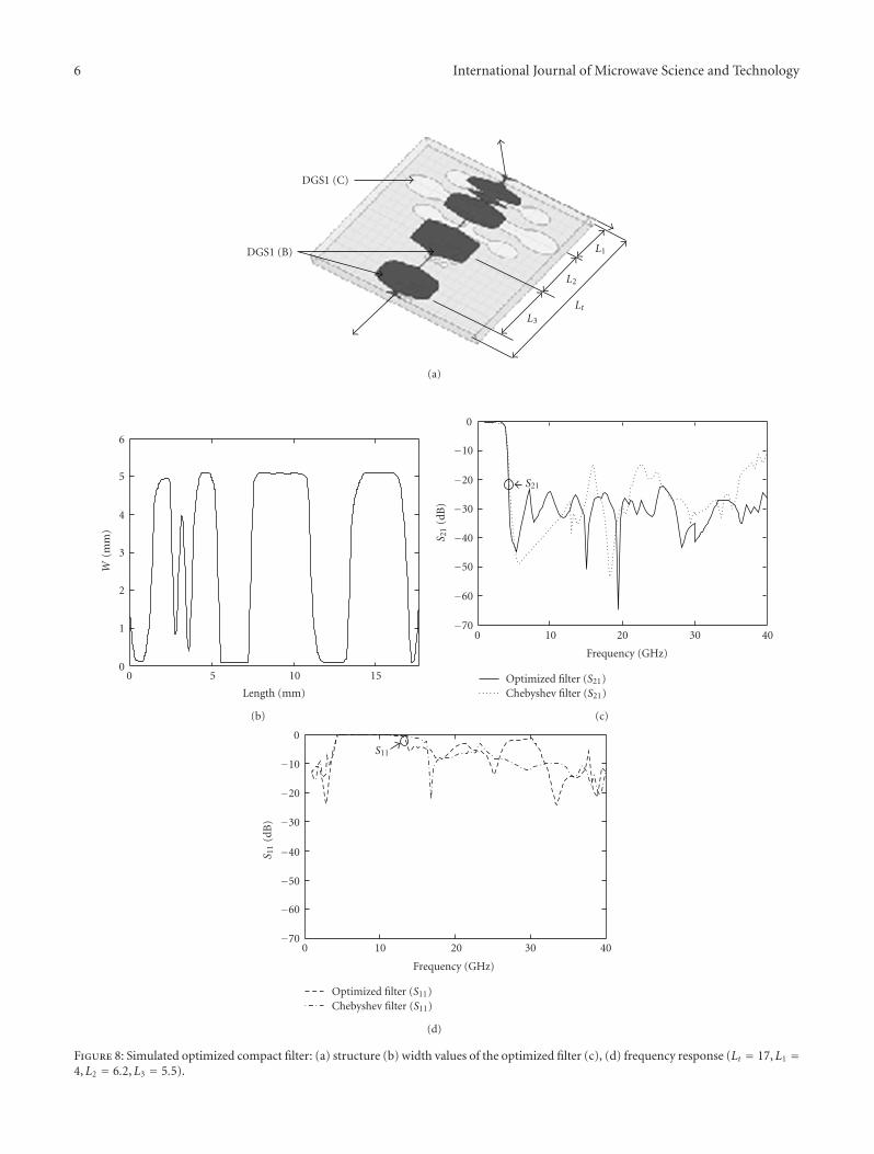
Figure 8: Simulated optimized compact filter: (a) structure (b) width values of the optimized filter (c), (d) frequency response (Lt = 17,L1 =4,L2 = 6.2,L3 = 5.5).

International Journal of Microwave Science and Technology 7
L3
L4
L1
L2
DGS1 (A)
DGS2 (A)
(a)
1000 6000 11000 16000 21000 25000−70
−60
−50
−40
−30
−20
−10
0
S 21
(dB
)
Frequency (MHz)
L1 = 19 mmL1 = 18 mm L1 = 36 mm
L1 = 18 mm, L2 = 36 mm
(b)
Figure 9: Setting up the cutoff frequency of the optimized filter: (a)the structure and (b) the frequency responses when (L3 = 5,L4 =25).
extracted from an electromagnetic simulation employing aButterworth bandstop filter response. Figure 5 depicts thefrequency responses of the DGSs. Various dimensions of therequired DGSs have been listed in Table 1.
5. Experimental Results
In order to show the effectiveness of the proposed methodand the accuracy of the model, we present experimentalresults. Figures 6 and 7 illustrate photos of the fabricatedfilter, the dimensions of structures, and their frequencyresponses. The DGS elements are cascaded in order torealize wider stopband with very sharp edge filter. The mea-surements are performed with an Agilent-8722ES networkanalyzer. CST 2008 and Ansoft Designer 4 use differentnumerical techniques to simulate the structures. Variationsin the measured performance are mainly due to imprecisefabrication by a milling machine, the effect of SMA con-nectors, and the nonideal soldering. Also, because of thelimitations in practical implementation, we were forced touse Rogers RT/duroid 6006 (TM) with a dielectric constant
Table 1: Dimensions (in mm) of DGSs with different resonantfrequencies.
DGS structures DGS (1) DGS (2)
Case A
R1 = 1, R2 = 0.75, R3 = 0.5 R1 = 1
D1 = 6, D2 = 4.3, D3 = 1, D1 = 1
D4 = 2.6, D5 = 4, D6 = 0.5, D2 = 3.3
D7 = 0.4, D8 = 2.2 D3 = 5
Case B
R1 = 0.5, R2 = 0.4,
R3 = 0.25,D1 = 3.2,
D2 = 2.2, D3 = 0.5,
D4 = 1.3, D5 = 2.2,
D6 = 0.25,D7 = 0.2,
D8 = 1.1
Case C
R1 = 2.25, R2 = 1.8,
R3 = 1.2,D1 = 14, D2 = 9.6,
D3 = 1.1, D4 = 5.8, D5 = 9.4,
D6 = 0.55, D7 = 0.9, D8 = .5
of 6.15. The simulation results show that the proposedstructure has an ultra-wide stopband and its peak remainsbelow the acceptable −22 dB level from 4.5 up to 60 GHz.
The operational frequency range of the Agilent-8722ESvector network analyzer was 50 MHz up to 40 GHz. There-fore, we were not able to measure the characteristics ofthe designed filter beyond 40 GHz. Also, only the S21 mea-surements were accessible. However, as it can be seen fromFigures 6 and 7, the simulation of the filter was performed upto 60 GHz using CST 2008 and Ansoft Designer 4 softwares.The structures were simulated with loss-free substrates andthe same results were obtained.
In another optimized structure, we present a morecompact design of the ultra-wide stopband lowpass filter.Figure 8 illustrates the dimensions and frequency response ofthe optimized compact filter. According to its specifications,a conventional 10th-order Chebyshev stepped-impedancelowpass microstrip filter is designed and optimized byAgilent ADS 2008 to highlight the performance of theoptimized filter. The conventional Chebyshev filter has32 mm length while the optimized filter’s length is less than ahalf-wavelength (i.e., 17 mm). The optimized compact filterhas sharper band edge and deeper and wider stopband.
In this case, the stopband peak is less than −21 dBfrom 4.3 up to 60 GHz. As mentioned earlier, a compactdeep attenuation and spurious-free filter is achieved by thismethod. The dimensions of the new DGS configuration aredemonstrated in Figure 8(a) and Table 1.
One of the interesting results of using such structures isthe ability to set up the cutoff frequency of these filters upto hundreds of MHz only by displacing a few millimeters ofthe DGSs with respect to their current positions as shown inFigure 9. The changes in characteristic impedance will shiftthe cutoff frequency. It is proportional to geometry, size,the amount, and displacement of DGSs. A varactor-loadedresonator can be implemented to design a tunable and high-selective lowpass filter.
8 International Journal of Microwave Science and Technology
6. Conclusion
An adaptive genetic algorithm is combined with nonuniformtransmission line to optimize a tapered microstrip lowpassfilter. With the DGS configurations, the proposed structuredisplays an ultra-wide stopband with high attenuation withina small circuit area. By applying adaptive genetic algorithmsand DGSs, the performance of a tapered microstrip filteris significantly improved. Also, the proposed lowpass filtershave wider and deeper stopband characteristics compared tothose of conventional lowpass ones. The equivalent circuitsand the related design procedures have been discussedin details. Numerical simulations using CST MicrowaveStudio 2008 and Ansoft Designer 4 show promising agree-ment with experiments. The measured data for fabricatedDGS-based lowpass filters have fairly good insertion-losscharacteristics. The designed filters have a 4 GHz cutofffrequency and also a stopband attenuation less than −21 dBfrom 4.3 GHz up to 60 GHz. As a result now, one candesign a desired compact filter, starting from a predefinedstructure.
References
[1] J. S. Hong and M. J. Lancaster, Microstrip Filters forRF/Microwave Applications, John Wiley & Sons, New York, NY,USA, 2001.
[2] J.-Z. Gu, W.-Y. Yin, R. Qian, C. Wang, and X.-W. Sun,“A wideband EBG structure with 1D compact microstripresonant cell,” Microwave and Optical Technology Letters, vol.45, no. 5, pp. 386–387, 2005.
[3] M. K. Mandal and S. Sanyal, “Compact wideband bandpassfilter,” IEEE Microwave and Wireless Components Letters, vol.16, no. 1, pp. 46–48, 2006.
[4] S. Sun and L. Zhu, “Capacitive-ended interdigital coupledlines for UWB bandpass filters with improved out-of-bandperformances,” IEEE Microwave and Wireless ComponentsLetters, vol. 16, no. 8, pp. 440–442, 2006.
[5] N. H. Younan, B. L. Cox, C. D. Taylor, and W. D. Prather,“Exponentially tapered transmission line antenna,” IEEETransactions on Electromagnetic Compatibility, vol. 36, no. 2,pp. 141–144, 1994.
[6] C. E. Baum and J. M. Lehr, “Tapered transmission-line trans-formers for fast high-voltage transients,” IEEE Transactions onPlasma Science, vol. 30, no. 5, pp. 1712–1721, 2002.
[7] L. A. Hayden and V. K. Tripathi, “Nonuniformly coupledmicrostrip transversal filters for analog signal processing,”IEEE Transactions on Microwave Theory and Techniques, vol.39, no. 1, pp. 47–53, 1991.
[8] A. E. Eiben, R. Hinterding, and Z. Michalewicz, “Parametercontrol in evolutionary algorithms,” IEEE Transactions onEvolutionary Computation, vol. 3, no. 2, pp. 124–141, 1999.
[9] D. Thierens, “An adaptive pursuit strategy for allocatingoperator probabilities,” in Proceedings of the ACM Genetic andEvolutionary Computation Conference (GECCO ’05), pp. 1539–1546, 2005.
[10] M. A. G. Laso, T. Lopetegi, M. J. Erro, D. Benito, M. J.Garde, and M. Sorolla, “Multiple-frequency-tuned photonicbandgap microstrip structures,” IEEE Microwave and WirelessComponents Letters, vol. 10, no. 6, pp. 220–222, 2000.
[11] C. C. Chiau, X. Chen, and C. Parini, “Multiperiod EBGstructure for wide stopband circuits,” IEE Proceedings, vol. 150,no. 6, pp. 489–492, 2003.
[12] Y.-C. Chen, A.-S. Liu, and R.-B. Wu, “A wide-stopbandlow-pass filter design based on multi-period taper-etchedEBG structure,” in Proceedings of the Asia-Pacific MicrowaveConference Proceedings (APMC ’05), vol. 3, pp. 2125–2127,Suzhou, China, December 2005.
[13] M. K. Mandal and S. Sanyal, “A novel defected groundstructure for planar circuits,” IEEE Microwave and WirelessComponents Letters, vol. 16, no. 2, pp. 93–95, 2006.
[14] Y. Chung, S.-S. Jeon, D. Ahn, J.-I. Choi, and T. Itoh,“High isolation dual-polarized patch antenna using integrateddefected ground structure,” IEEE Microwave and WirelessComponents Letters, vol. 14, no. 1, pp. 4–6, 2004.
[15] Z. Pan and J. Wang, “Design of the UWB bandpass filterby coupled microstrip lines with U-shaped defected groundstructure,” in Proceedings of the International Conference onMicrowave and Millimeter Wave Technology (ICMMT ’08), vol.1, pp. 329–332, April 2008.
[16] T. Kido, H. Deguchi, M. Tsuji, and M. Ohira, “Compacthigh-performance planar bandpass filters with arbitrarily-shaped conductor patches and slots,” in Proceedings of the 38thEuropean Microwave Conference (EuMC ’08), pp. 1165–1168,October 2008.
[17] C.-S. Kim, J.-S. Park, D. Ahn, and J.-B. Lim, “A novel 1-Dperiodic defected ground structure for planar circuits,” IEEEMicrowave and Wireless Components Letters, vol. 10, no. 4, pp.131–133, 2000.
[18] R. E. Collin, Foundations for Microwave Engineering, McGraw-Hill, New York, NY, USA, 2nd edition, 2000.
[19] K. Lu, “An efficient method for analysis of arbitrary nonuni-form transmission lines,” IEEE Transactions on MicrowaveTheory and Techniques, vol. 45, no. 1, pp. 9–14, 1997.
[20] C. L. Edwards, M. L. Edwards, S. Cheng, R. K. Stilwell, andC. C. Davis, “A simplified analytic CAD model for linearlytapered microstrip lines including losses,” IEEE Transactionson Microwave Theory and Techniques, vol. 52, no. 3, pp. 823–830, 2004.
[21] M.-I. Lai and S.-K. Jeng, “Compact microstrip dual-bandbandpass filters design using genetic-algorithm techniques,”IEEE Transactions on Microwave Theory and Techniques, vol.54, no. 1, pp. 160–168, 2006.
[22] E. Michielssen, J.-M. Sajer, S. Ranjithant, and R. Mittra,“Design of lightweight, broad-band microwave absorbersusing genetic algorithms,” IEEE Transactions on MicrowaveTheory and Techniques, vol. 41, no. 6-7, pp. 1024–1030, 1993.
[23] T. Nishino and T. Itoh, “Evolutionary generation of microwaveline-segment circuits by genetic algorithms,” IEEE Transac-tions on Microwave Theory and Techniques, vol. 50, no. 9, pp.2048–2055, 2002.
[24] M. Srinivas and L. M. Patnaik, “Adaptive probabilities ofcrossover and mutation in genetic algorithms,” IEEE Transac-tions on Systems, Man and Cybernetics, vol. 24, no. 4, pp. 656–667, 1994.
[25] C.-L. Liu, Z.-Y. Wang, and Z. Bao, “A kind of adaptive geneticalgorithm and it’s application in model identification,” inProceedings of the 4th International Conference on MachineLearning and Cybernetics (ICMLC ’05), vol. 5, pp. 2865–2869,August 2005.
[26] B. T. Skinner, H. T. Nguyen, and D. K. Liu, “Performancestudy of a multi-deme parallel genetic algorithm with adaptive

International Journal of Microwave Science and Technology 9
mutation,” in Proceedings of the 2nd International Conferenceon Autonomous Robots and Agents, Palmerston North, NewZealand, December 2004.
[27] T. C. Edwards and M. B. Steer, Foundations of Interconnect andMicrostrip Design, John Wiley & Sons, New York, NY, USA, 3rdedition, 2000.

Submit your manuscripts athttp://www.hindawi.com
VLSI Design
Hindawi Publishing Corporationhttp://www.hindawi.com Volume 2014
International Journal of
RotatingMachinery
Hindawi Publishing Corporationhttp://www.hindawi.com Volume 2014
Hindawi Publishing Corporation http://www.hindawi.com
Journal ofEngineeringVolume 2014
Hindawi Publishing Corporationhttp://www.hindawi.com Volume 2014
Shock and Vibration
Hindawi Publishing Corporationhttp://www.hindawi.com Volume 2014
Mechanical Engineering
Advances in
Hindawi Publishing Corporationhttp://www.hindawi.com Volume 2014
Civil EngineeringAdvances in
Advances inAcoustics &Vibration
Hindawi Publishing Corporationhttp://www.hindawi.com Volume 2014
Hindawi Publishing Corporationhttp://www.hindawi.com Volume 2014
Electrical and Computer Engineering
Journal of
Hindawi Publishing Corporationhttp://www.hindawi.com Volume 2014
DistributedSensor Networks
International Journal of
The Scientific World JournalHindawi Publishing Corporation http://www.hindawi.com Volume 2014
Hindawi Publishing Corporationhttp://www.hindawi.com Volume 2014
Journal of
Sensors
Modelling & Simulation in EngineeringHindawi Publishing Corporation http://www.hindawi.com Volume 2014
Hindawi Publishing Corporationhttp://www.hindawi.com Volume 2014
Active and Passive Electronic Components
Advances inOptoElectronics
Hindawi Publishing Corporation http://www.hindawi.com
Volume 2014
RoboticsJournal of
Hindawi Publishing Corporationhttp://www.hindawi.com Volume 2014
Chemical EngineeringInternational Journal of
Hindawi Publishing Corporationhttp://www.hindawi.com Volume 2014
Control Scienceand Engineering
Journal of
Hindawi Publishing Corporationhttp://www.hindawi.com Volume 2014
International Journal of
Antennas andPropagation
Hindawi Publishing Corporation http://www.hindawi.com Volume 2014
Hindawi Publishing Corporationhttp://www.hindawi.com Volume 2014
Navigation and Observation
International Journal of
Copyright © 2022 FDOKUMEN