On airborne nano/micro-sized wear particles released from low-metallic automotive brakes
Upload
khangminh22Category
view
3download
0
Micro/Nano Manufacturing
Hans Nørgaard Hansen and Guido Tosello
www.mdpi.com/journal/micromachines
Edited by
Printed Edition of the Special Issue Published in Micromachines

Micro/Nano Manufacturing
Special Issue Editors Hans Nørgaard Hansen
Guido Tosello
MDPI • Basel • Beijing • Wuhan • Barcelona • Belgrade

Special Issue Editors
Hans Nørgaard Hansen Guido Tosello
Technical University of Denmark Technical University of Denmark
Denmark Denmark
Editorial Office
MDPI AG
St. Alban-Anlage 66
Basel, Switzerland
This edition is a reprint of the Special Issue published online in the open access
journal Micromachines (ISSN 2072-666X) in 2017 (available at: http://www.mdpi.com/ journal/micromachines/special_issues/micro_nano_manufacturing).
For citation purposes, cite each article independently as indicated on the article
page online and as indicated below:
Author 1; Author 2. Article title. Journal Name Year, Article number, page range.
First Edition 2017
ISBN 978-3-03842-604-2 (Pbk)
ISBN 978-3-03842-605-9 (PDF)
Articles in this volume are Open Access and distributed under the Creative Commons Attribution license (CC BY), which allows users to download, copy and build upon published articles even for commercial purposes, as long as the author and publisher are properly credited, which ensures maximum dissemination and a wider impact of our publications. The book taken as a whole is © 2017 MDPI, Basel, Switzerland, distributed under the terms and conditions of the Creative Commons license CC BY-NC-ND (http://creativecommons.org/licenses/by-nc-nd/4.0/).

iii
Table of Contents
About the Special Issue Editors ................................................................................................................... v
Preface to “Micro/Nano Manufacturing” ................................................................................................... vii
Emanuele Cannella, Emil Krabbe Nielsen and Alessandro Stolfi
Designing a Tool System for Lowering Friction during the Ejection of In-Die Sintered
Micro Gears
Reprinted from: Micromachines 2017, 8(7), 214; doi: 10.3390/mi8070214 ............................................... 1
J. Israel Martínez-López, H.A. Betancourt, Erika García-López, Ciro A. Rodriguez
and Hector R. Siller
Rapid Fabrication of Disposable Micromixing Arrays Using Xurography and Laser Ablation
Reprinted from: Micromachines 2017, 8(5), 144; doi: 10.3390/mi8050144 ............................................... 16
Toshiyuki Obikawa and Mamoru Hayashi
Ultrasonic-Assisted Incremental Microforming of Thin Shell Pyramids of Metallic Foil Reprinted from: Micromachines 2017, 8(5), 142; doi: 10.3390/mi8050142 ............................................... 30
Matthew Bahr, Yasa Sampurno, Ruochen Han and Ara Philipossian
Slurry Injection Schemes on the Extent of Slurry Mixing and Availability during Chemical Mechanical Planarization
Reprinted from: Micromachines 2017, 8(6), 170; doi: 10.3390/mi8060170 ............................................... 40
Nicolas Blondiaux, Raphaël Pugin, Gaëlle Andreatta, Lionel Tenchine, Stéphane Dessors,
Pierre-François Chauvy, Matthieu Diserens and Philippe Vuillermoz
Fabrication of Functional Plastic Parts Using Nanostructured Steel Mold Inserts
Reprinted from: Micromachines 2017, 8(6), 179; doi: 10.3390/mi8060179 ............................................... 52
Cheng Guo, Jun Qian and Dominiek Reynaerts
Fabrication of Mesoscale Channel by Scanning Micro Electrochemical Flow Cell (SMEFC) Reprinted from: Micromachines 2017, 8(5), 143; doi: 10.3390/mi8050143 ............................................... 65
Federico Baruffi, Paolo Parenti, Francesco Cacciatore, Massimiliano Annoni
and Guido Tosello
On the Application of Replica Molding Technology for the Indirect Measurement of Surface and Geometry of Micromilled Components
Reprinted from: Micromachines 2017, 8(6), 195; doi: 10.3390/mi8060195 ............................................... 86
Axiu Cao, Hui Pang, Jiazhou Wang, Man Zhang, Jian Chen, Lifang Shi, Qiling Deng
and Song Hu
The Effects of Profile Errors of Microlens Surfaces on Laser Beam Homogenization
Reprinted from: Micromachines 2017, 8(2), 50; doi: 10.3390/mi8020050 ................................................. 104
Byungjoo Choi, Jiwoon Kwon, Yongho Jeon and Moon Gu Lee
Development of Novel Platform to Predict the Mechanical Damage of a Miniature Mobile Haptic Actuator
Reprinted from: Micromachines 2017, 8(5), 156; doi: 10.3390/mi8050156 ............................................... 112

iv
Lili Gao, Zai-Fa Zhou and Qing-An Huang
Modeling of the Effect of Process Variations on a Micromachined Doubly-Clamped Beam
Reprinted from: Micromachines 2017, 8(3), 81; doi: 10.3390/mi8030081 ................................................. 124
Tatsuhiko Aizawa and Kenji Wasa
Low Temperature Plasma Nitriding of Inner Surfaces in Stainless Steel Mini-/Micro-Pipes
and Nozzles
Reprinted from: Micromachines 2017, 8(5), 157; doi: 10.3390/mi8050157 ............................................... 139
Ali Davoudinejad, Guido Tosello, Paolo Parenti and Massimiliano Annoni
3D Finite Element Simulation of Micro End-Milling by Considering the Effect of Tool Run-Out Reprinted from: Micromachines 2017, 8(6), 187; doi: 10.3390/mi8060187 ............................................... 148
Philipp Wilhelmi, Christian Schenck and Bernd Kuhfuss
Handling in the Production of Wire-Based Linked Micro Parts
Reprinted from: Micromachines 2017, 8(6), 169; doi: 10.3390/mi8060169 ............................................... 168
v
About the Special Issue Editors Hans Nørgaard Hansen is working in the field of Micro/Nano Manufacturing. He deals with establishing the basis of industrial production of products and components in metal, polymers and ceramics in the micro‐ and nanometer regime. Specific activities include product development, materials development and development of processes and production systems focused on micro mechanical systems. The core activities comprise micro product design and development, tooling technologies for micro injection moulding and micro metal forming, mass production technologies, chemical and electrochemical processes and laser technologies. Finally the integration of processes into coherent process chains is a key activity. Professor Hans Nørgaard Hansen is the Head of the Department of Mechanical Engineering at the Technical University of Denmark, is a Fellow of CIRP (International Academy of Production Engineering) and the 2015–2017 President of euspen (European Society of Precision Engineering and Nanotechnology). Guido Tosello is Associate Professor at the Technical University of Denmark, Department of Mechanical Engineering, Section of Manufacturing Engineering. Guidoʹs principal research interests are the analysis, characterization, monitoring, control, optimization and simulation of precision moulding processes at micro/nano scales of thermoplastic materials. Technologies supporting precision/micro/nano moulding processes are of research interest: advanced process chain for micro/nano tools manufacturing, precision and micro additive manufacturing, dimensional and surface micro/nano metrology. Guido Tosello is the recipient of the ʺTechnical University of Denmark Best PhD Research Work 2008 Prizeʺ for his PhD thesis “Precision Moulding of Polymer Micro Components”, of the 2012 Alan Glanvill Award by The Institute of Materials, Minerals and Mining (IOM3) (UK), given as recognition for research of merit in the field of polymeric materials, of the Young Research Award 2014 from the Polymer Processing Society (USA) in recognition of scientific achievements and research excellence in polymer processing within 6 years from PhD graduation, and of the Outstanding Reviewer Award 2016 of the Institute of Physics (UK) for his contribution to the Journal of Microengineering and Micromechanics. Guido Tosello is currently the Project Coordinator of the Horizon2020 European Marie Skłodowska‐Curie Innovative Training Network MICROMAN “Process Fingerprint for Zero‐defect Net‐shape MICROMANufacturing” (2015–2019).


vii
Preface to “Micro/Nano Manufacturing”
Micro- and nano-scale manufacturing has been the subject of an increasing amount of interest and research efforts worldwide in both academia and industry over the past 10 years. Traditional lithography-
based technology forms the basis of silicon-based micro-electro-mechanical systems (MEMS) manufacturing, but also precision manufacturing technologies have been developed to cover micro-scale
dimensions and accuracies. Furthermore, these fundamentally different technology ecosystems are currently combined in order to exploit the strengths of both platforms. One example is the use of lithography-based technologies to establish nanostructures that are subsequently transferred to 3D geometries via injection molding.
Manufacturing processes at the micro-scale are the key-enabling technologies to bridge the gap between the nano- and the macro-worlds, to increase the accuracy of micro/nano-precision production
technologies, and to integrate different dimensional scales in mass-manufacturing processes. Accordingly, the present Special Issue provides recent developments in the field of micro/nano manufacturing in terms of production techniques and key enabling technologies that push the boundaries of the state of the art mass-manufacturing of micro-scale and micro/nano structured components.
The Special Issue consists of 13 original research papers, which cover both fundamental process technology developments as well as the application of those technologies for the fabrication of micro/nano devices. The papers included in this Special Issue address research in four main domains of micro/nano manufacturing:
(1) Process developments of micro-scale fabrication methods. Cannella et al. [1] developed a novel tooling system for in-die sintering of micro metal gears; Martinez-López et al. [2] investigated xurography and laser ablation processes for the rapid fabrication of micromixing arrays; Obikawa et al. [3] demonstrated ultrasonic-assisted incremental microforming for the rapid prototyping of thin shell metal pyramids.
(2) Micro/nano manufacturing technologies based on electrochemical processing. Bahr et al. [4] investigated the slurry application and injection system to advance the performance of the Chemical Mechanical Planarization (CMP) process; Blondiaux et al. [5] realized the fabrication of nanostructured steel mold inserts by applying a combination of nanosphere lithography and electrochemical etching; Guo et al. [6] demonstrated the fabrication of mesoscale channels by applying a micro electrochemical machining (µECM) process based on the scanning micro electrochemical flow cell (SMEFC).
(3) Quality control of micro systems and processes. Baruffi et al. [7] demonstrated the application of the replica molding technology for quality control of micro milled surfaces; Cao et al. [8] investigated the effect of profile errors on the surface of micro lenses on laser beam homogenization; Choi et al. [9] presented a novel testing platform to characterize and predict the mechanical damage of miniaturized haptic actuator; Gao et al. [10] modeled the effect of micro manufacturing process variations on the characteristics of a micro machined doubly-clamped beam.
(4) Key enabling technologies for micro production. Aizawa et al. [11] presented the development of low-temperature plasma nitriding for the treatment of stainless miniaturized pipes and nozzles’ internal surfaces; Davoudinejad et al. [12] modeled and simulated the micro end-milling process including the effect of tool run-out; Wilhelmi et al. [13] demonstrated the improvements in multi-stage micro production by handling wire-based linked micro parts.
We wish to thank all authors who submitted their papers to the Special Issue “Micro/Nano Manufacturing”. We would also like to acknowledge all the reviewers whose careful and timely reviews ensured the quality of this Special Issue.

viii
References
1. Cannella, E.; Nielsen, E.; Stolfi, A. Designing a Tool System for Lowering Friction during the Ejection of In-Die Sintered Micro Gears. Micromachines 2017, 8, 214; doi:10.3390/mi8070214.
2. Martínez-López, J.; Betancourt, H.; García-López, E.; Rodriguez, C.; Siller, H. Rapid Fabrication of Disposable Micromixing Arrays Using Xurography and Laser Ablation. Micromachines 2017, 8, 144; doi:10.3390/mi8050144.
3. Obikawa, T.; Hayashi, M. Ultrasonic-Assisted Incremental Microforming of Thin Shell Pyramids of Metallic Foil. Micromachines 2017, 8, 142; doi:10.3390/mi8050142.
4. Bahr, M.; Sampurno, Y.; Han, R.; Philipossian, A. Slurry Injection Schemes on the Extent of Slurry Mixing and Availability during Chemical Mechanical Planarization. Micromachines 2017, 8, 170;
doi:10.3390/mi8060170. 5. Blondiaux, N.; Pugin, R.; Andreatta, G.; Tenchine, L.; Dessors, S.; Chauvy, P.; Diserens, M.;
Vuillermoz, P. Fabrication of Functional Plastic Parts Using Nanostructured Steel Mold Inserts. Micromachines 2017, 8, 179; doi:10.3390/mi8060179.
6. Guo, C.; Qian, J.; Reynaerts, D. Fabrication of Mesoscale Channel by Scanning Micro Electrochemical Flow Cell (SMEFC). Micromachines 2017, 8, 143; doi:10.3390/mi8050143.
7. Baruffi, F.; Parenti, P.; Cacciatore, F.; Annoni, M.; Tosello, G. On the Application of Replica Molding Technology for the Indirect Measurement of Surface and Geometry of Micromilled Components. Micromachines 2017, 8, 195; doi:10.3390/mi8060195.
8. Cao, A.; Pang, H.; Wang, J.; Zhang, M.; Chen, J.; Shi, L.; Deng, Q.; Hu, S. The Effects of Profile Errors of Microlens Surfaces on Laser Beam Homogenization. Micromachines 2017, 8, 50;
doi:10.3390/mi8020050. 9. Choi, B.; Kwon, J.; Jeon, Y.; Lee, M. Development of Novel Platform to Predict the Mechanical
Damage of a Miniature Mobile Haptic Actuator. Micromachines 2017, 8, 156;
doi:10.3390/mi8050156. 10. Gao, L.; Zhou, Z.; Huang, Q. Modeling of the Effect of Process Variations on a Micromachined
Doubly-Clamped Beam. Micromachines 2017, 8, 81; doi:10.3390/mi8030081. 11. Aizawa, T.; Wasa, K. Low Temperature Plasma Nitriding of Inner Surfaces in Stainless Steel
Mini-/Micro-Pipes and Nozzles. Micromachines 2017, 8, 157; doi:10.3390/mi8050157. 12. Davoudinejad, A.; Tosello, G.; Parenti, P.; Annoni, M. 3D Finite Element Simulation of Micro
End-Milling by Considering the Effect of Tool Run-Out. Micromachines 2017, 8, 187;
doi:10.3390/mi8060187. 13. Wilhelmi, P.; Schenck, C.; Kuhfuss, B. Handling in the Production of Wire-Based Linked Micro
Parts. Micromachines 2017, 8, 169; doi:10.3390/mi8060169.
Hans Nørgaard Hansen and Guido Tosello
Special Issue Editors


micromachines
Article
Designing a Tool System for Lowering Frictionduring the Ejection of In-Die Sintered Micro Gears
Emanuele Cannella 1,2,* , Emil Krabbe Nielsen 3 and Alessandro Stolfi 2
1 IPU Product Development, Kgs. Lyngby 2800 DK, Denmark2 DTU Department of Mechanical Engineering, Kgs. Lyngby 2800 DK, Denmark; [email protected] DTU Department of Electrical Engineering, Kgs. Lyngby 2800 DK, Denmark; [email protected]* Correspondence: [email protected]; Tel.: +45-4525-6286
Received: 29 May 2017; Accepted: 3 July 2017; Published: 6 July 2017
Abstract: The continuous improvements in micro-forging technologies generally involve process,material, and tool design. The field assisted sintering technique (FAST) is a process that makespossible the manufacture of near-net-shape components in a closed-die setup. However, the final partquality is affected by the influence of friction during the ejection phase, caused by radial expansionof the compacted and sintered powder. This paper presents the development of a pre-stressed toolsystem for the manufacture of micro gears made of aluminum. By using the hot isostatic pressing(HIP) sintering process and different combinations of process parameters, the designed tool systemwas compared to a similar tool system designed without a pre-stressing strategy. The comparisonbetween the two tool systems was based on the ejection force and part fidelity. The ejection force wasmeasured during the tests, while the part fidelity was documented using an optical microscope andcomputed tomography in order to obtain a multi-scale characterization. The results showed that theuse of pre-stress reduced the porosity in the gear by 40% and improved the dimensional fidelity bymore than 75% compared to gears produced without pre-stress.
Keywords: micro sintering; field assisted sintering technique; hot isostatic pressing; micro gears;computed tomography; dimensional accuracy; porosity analysis
1. Introduction
Micro-sintering enables the manufacture of micro-scale components with a complex shapeand geometry. Near-net-shape components can be easily manufactured and post-removal processes,e.g., grinding, are limited to the final surface polishing. Compared to cutting processes, since thematerial scrap is reduced, a high saving of material is possible. Generally, the conventional sinteringprocess can be considered as two different phases, i.e., compaction and heating of the powder [1].The powder is fed into a closed-die and the punches apply the desired pressure to compact the rawmaterial. The compacted sample, called “green compact”, is ejected from the die and moved into atemperature-controlled oven. The sintering temperature is a process parameter and is strictly dependenton the material. This value never overcomes the melting temperature of the material. Therefore, thegreen compact is kept inside the oven for a defined time, namely the “sintering time”. In a finalphase, the sample is moved out from the oven and cooled down to the room temperature. The wholeprocess makes it possible to enable the densification of the sample by diffusional mechanisms issuedfrom the pressure and high temperature. Since, in the sintering process, the two steps, i.e., heatingand compaction, are carried out separately, the manufacturing time per component is extended.Additionally, oxidation of the material may occur and a protective atmosphere is required to preventthis phenomenon.
Micromachines 2017, 8, 214 1 www.mdpi.com/journal/micromachines
Micromachines 2017, 8, 214
To decrease the sintering time per component, new sintering processes have been developed.Such processes conduct heating and compaction of the powder simultaneously, thereby reducingmanufacturing time and improving the densification of the component [2–4]. Such new sinteringprocesses establish a mechanical-thermal field, which enables a different bonding mechanism betweenthe powder particles [5–7]. Hot isostatic pressing (HIP) and field assisted sintering technology(FAST) [8–10], are the main names given to such sintering processes. The main difference is onthe kind of heating principle [11]. In the HIP sintering, an external heating element, e.g., a heatingnozzle, provides the sintering of the pressed compact. In FAST sintering, the sintering heat is providedfrom the electrical current generating Joule heating while flowing into the compactor and/or thedie [12,13]. FAST and HIP operate both the compaction and heating operations inside the closed-diesetup. Since the compacted and heated powder cannot expand radially in such a setup, both sinteringapproaches generate a radial pressure at the die/sample interface. The radial pressure is mainly causedby the axial compaction pressure and thermal heating. The theoretical models, studied by Long andBockstiegel [14,15], allow an estimation of the radial pressure caused from the axial compaction of thepowder. The thermal influence on the radial pressure is studied by applying the thermal expansionlaw. The radial pressure has a direct impact on the quality of the sintered part because it increases thefriction at the interface and, thus, the ejection force. Additionally, the “spring-back” effect may furtheraffect the quality of the sintered component [16]. Several studies have investigated new solutions toreducing the friction, leading to four different types of approaches. A first approach relies on lubricants,which are commonly applied in conventional sintering. The majority of lubricants evaporate above atemperature of 200 ◦C, leaving, e.g., graphite or molybdenum disulfide as the only options. However,the use of lubricants influences the sample quality in terms of contamination, reducing the “greenstrength” and density [17–20]. A second approach is based on the use of a split die solution, where thedie includes several dismountable parts [21,22]. The latter are assembled before sintering and thendisassembled when the component is sintered and ready to be ejected. A third approach is based on atapered die solution that makes it possible to gradually decrease the radial pressure, thereby avoidingcrack formation [23]. The tapered dies are difficult to manufacture for their complex geometricalshapes. A fourth approach consists of the die pre-stressing, representing a solution being well-knownin metal forming. The die pre-stressing reduces the maximum tangential stress, known as the hoopstress, and the stress fluctuations, which the die is subject to. The use of the pre-stress for a sinteringtool was justified by the possibility of reducing the internal diameter of the die during the process.Starting from the estimation of the radial pressure, the expected radial expansion of the sample in afree-die wall condition can be predicted [14]. The pre-stress was then designed to achieve an internaldiameter reduction being equal to, or larger than, the sample expansion. After sintering, the stress-ringwas taken off and the pre-stress was removed from the die which, thus, recovers to the original innerdiameter. The radial pressure was decreased, thereby reducing the friction and ejection force. The diepre-stressing can be obtained using more than one approach e.g., stress-rings [24], stress-pins [25],stripwound containers [26], and a SMART® application using shape memory alloys (SMAs) [27,28].Each of the die pre-stressing solutions features advantages and disadvantages [26,29–31].
This paper presents the development of a pre-stressed tool system for the manufacture ofmicro-gears [32]. The developed pre-stressed tool system worked according to HIP. Fourteen gearswere produced using the pre-stressed tool system and then compared to other 14 gears producedwithout the stress-ring strategy. Different combinations of punch pressure, sintering temperature, andholding time were used to manufacture the gears. The comparison between the two tool systems wasbased on the ejection force and part fidelity to the computer-aided design (CAD) file. The ejection forcewas measured during the gear manufacture, while the part fidelity was documented using an opticalmicroscope and computed tomography in order to obtain a multi-scale characterization. Furthermore,porosity analysis was carried out on the gears using computed tomography.
2
Micromachines 2017, 8, 214
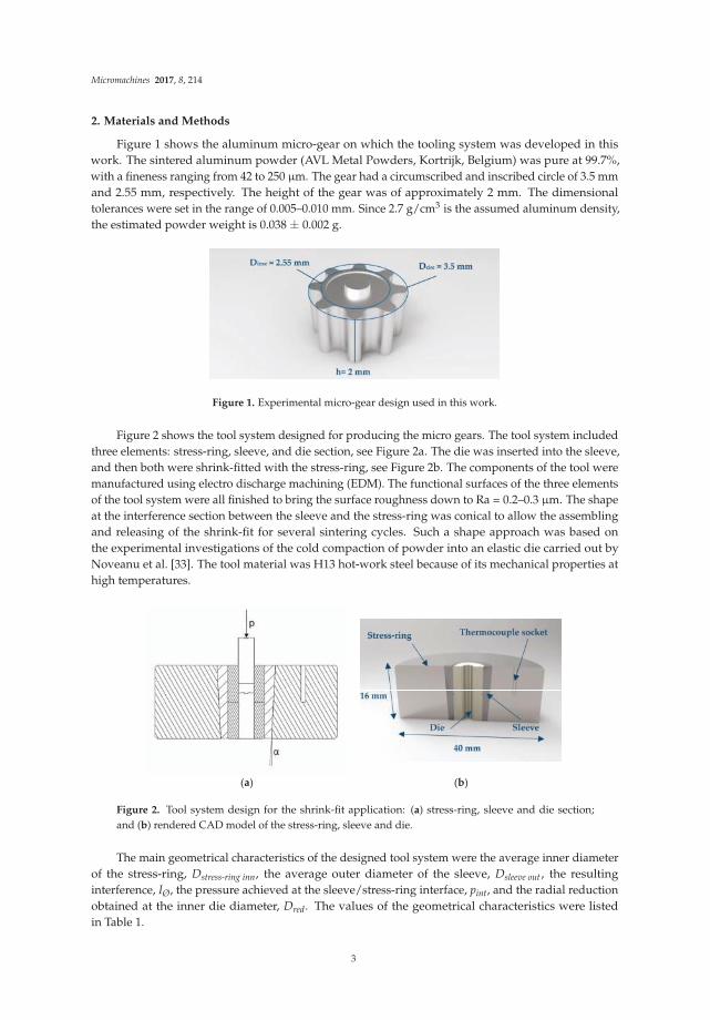
2. Materials and Methods
Figure 1 shows the aluminum micro-gear on which the tooling system was developed in thiswork. The sintered aluminum powder (AVL Metal Powders, Kortrijk, Belgium) was pure at 99.7%,with a fineness ranging from 42 to 250 µm. The gear had a circumscribed and inscribed circle of 3.5 mmand 2.55 mm, respectively. The height of the gear was of approximately 2 mm. The dimensionaltolerances were set in the range of 0.005–0.010 mm. Since 2.7 g/cm3 is the assumed aluminum density,the estimated powder weight is 0.038 ± 0.002 g.
Figure 1. Experimental micro-gear design used in this work.
Figure 2 shows the tool system designed for producing the micro gears. The tool system includedthree elements: stress-ring, sleeve, and die section, see Figure 2a. The die was inserted into the sleeve,and then both were shrink-fitted with the stress-ring, see Figure 2b. The components of the tool weremanufactured using electro discharge machining (EDM). The functional surfaces of the three elementsof the tool system were all finished to bring the surface roughness down to Ra = 0.2–0.3 µm. The shapeat the interference section between the sleeve and the stress-ring was conical to allow the assemblingand releasing of the shrink-fit for several sintering cycles. Such a shape approach was based onthe experimental investigations of the cold compaction of powder into an elastic die carried out byNoveanu et al. [33]. The tool material was H13 hot-work steel because of its mechanical properties athigh temperatures.
(a) (b)
Figure 2. Tool system design for the shrink-fit application: (a) stress-ring, sleeve and die section;and (b) rendered CAD model of the stress-ring, sleeve and die.
The main geometrical characteristics of the designed tool system were the average inner diameterof the stress-ring, Dstress-ring inn, the average outer diameter of the sleeve, Dsleeve out , the resultinginterference, IØ, the pressure achieved at the sleeve/stress-ring interface, pint, and the radial reductionobtained at the inner die diameter, Dred. The values of the geometrical characteristics were listedin Table 1.
3
Micromachines 2017, 8, 214
Table 1. Dimensional specifications of the pre-stressed tool.
Dstress-ring inn Dsleeve out IØ pint Dred
11.95 mm 12.00 mm 0.05 mm 326 MPa 12 µm
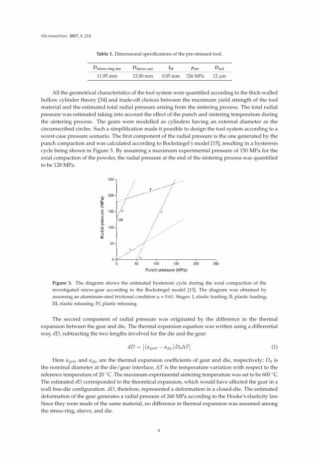
All the geometrical characteristics of the tool system were quantified according to the thick-walledhollow cylinder theory [34] and trade-off choices between the maximum yield strength of the toolmaterial and the estimated total radial pressure arising from the sintering process. The total radialpressure was estimated taking into account the effect of the punch and sintering temperature duringthe sintering process. The gears were modelled as cylinders having an external diameter as thecircumscribed circles. Such a simplification made it possible to design the tool system according to aworst-case pressure scenario. The first component of the radial pressure is the one generated by thepunch compaction and was calculated according to Bockstiegel’s model [15], resulting in a hysteresiscycle being shown in Figure 3. By assuming a maximum experimental pressure of 150 MPa for theaxial compaction of the powder, the radial pressure at the end of the sintering process was quantifiedto be 128 MPa.
Figure 3. The diagram shows the estimated hysteresis cycle during the axial compaction of theinvestigated micro-gear according to the Bockstiegel model [15]. The diagram was obtained byassuming an aluminum-steel frictional condition µ = 0.61. Stages: I, elastic loading; II, plastic loading;III, elastic releasing; IV, plastic releasing.
The second component of radial pressure was originated by the difference in the thermalexpansion between the gear and die. The thermal expansion equation was written using a differentialway, dD, subtracting the two lengths involved for the die and the gear:
dD =∣
∣
(
αgear − αdie
)
D0∆T∣
∣ (1)
Here αgear and αdie are the thermal expansion coefficients of gear and die, respectively; D0 isthe nominal diameter at the die/gear interface; ∆T is the temperature variation with respect to thereference temperature of 20 ◦C. The maximum experimental sintering temperature was set to be 600 ◦C.The estimated dD corresponded to the theoretical expansion, which would have affected the gear in awall free-die configuration. dD, therefore, represented a deformation in a closed-die. The estimateddeformation of the gear generates a radial pressure of 260 MPa according to the Hooke’s elasticity law.Since they were made of the same material, no difference in thermal expansion was assumed amongthe stress-ring, sleeve, and die.
4
Micromachines 2017, 8, 214
The total radial pressure was quantified to be 388 MPa by summing the two above mentionedcontributions, leading to a theoretical diameter expansion of the gear, Dexp, in a case of wall-freedie [14] as follows:
Dexp =pr − νpr − νpa
ED0 (2)
where pr is the total radial pressure previously calculated; pa is the axial compaction pressure; ν is thePoisson’s ratio; E is the Young’s modulus of aluminum. The Dexp value was found to be 13.48 µm.The nearest value to the Dexp value, complying with the yield limit of the used tool material, waschosen as the Dred.
Visual inspections and computed tomography inspections were carried out on the manufacturedgears. Visual inspections were carried out to evaluate the impact of the reduction of the ejection forceon the surface of the gears using an optical microscope DeMeet-220 (Schut Geometrical Metrology,Groningen, The Netherlands) with a 5:1 lens. The same lighting, fixturing process, and inspection areawere used for all the inspected gears. The gears were gently cleaned before being inspected. Computedtomography (CT) inspections were, furthermore, carried out to evaluate the impact of the pre-stresson the resulting porosity and dimensional accuracy of the gears. CT is an imaging method that takesadvantage of the capability of X-rays to penetrate the material [35,36].
3. Experimental Setup
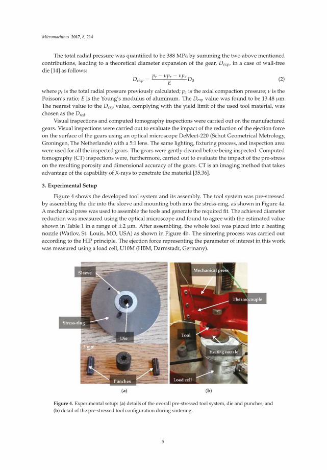
Figure 4 shows the developed tool system and its assembly. The tool system was pre-stressedby assembling the die into the sleeve and mounting both into the stress-ring, as shown in Figure 4a.A mechanical press was used to assemble the tools and generate the required fit. The achieved diameterreduction was measured using the optical microscope and found to agree with the estimated valueshown in Table 1 in a range of ±2 µm. After assembling, the whole tool was placed into a heatingnozzle (Watlov, St. Louis, MO, USA) as shown in Figure 4b. The sintering process was carried outaccording to the HIP principle. The ejection force representing the parameter of interest in this workwas measured using a load cell, U10M (HBM, Darmstadt, Germany).
Figure 4. Experimental setup: (a) details of the overall pre-stressed tool system, die and punches; and(b) detail of the pre-stressed tool configuration during sintering.
5
Micromachines 2017, 8, 214
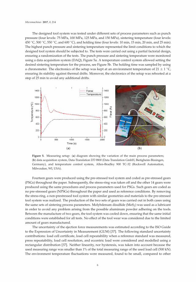
The designed tool system was tested under different sets of process parameters such as punchpressure (four levels: 75 MPa, 100 MPa, 125 MPa, and 150 MPa), sintering temperature (four levels:450 ◦C, 500 ◦C, 550 ◦C, and 600 ◦C), and holding time (four levels: 10 min, 15 min, 20 min, and 25 min).The highest punch pressure and sintering temperature represented the limit conditions to which thedesigned tool system should be subjected to. The tests were carried out using a partial factorial design,ensuring a randomization of the tests. The punch pressure and sintering temperature were monitoredusing a data acquisition system (DAQ), Figure 5a. A temperature control system allowed setting thedesired sintering temperature for the process, see Figure 5b. The holding time was sampled by usinga chronometer. The electronics of the setup was kept at an environment temperature of 21 ± 1 ◦C,ensuring its stability against thermal drifts. Moreover, the electronics of the setup was rebooted at astep of 25 min to avoid any additional drifts.
(a) (b)
Figure 5. Measuring setup: (a) diagram showing the variation of the main process parameters;(b) data acquisition system, Data-Translation DT-9800 (Data Translation GmbH, Bietigheim-Bissingen,Germany), and temperature control system, Allen-Bradley 900 TC-32 (Rockwell Automation,Milwaukee, WI, USA).
Fourteen gears were produced using the pre-stressed tool system and coded as pre-stressed gears(PSGs) throughout the paper. Subsequently, the stress-ring was taken off and the other 14 gears wereproduced using the same procedures and process parameters used for PSGs. Such gears are coded asno pre-stressed gears (NPSGs) throughout the paper and used as reference conditions. By removingthe stress-ring, a non-prestressed tool system with similar geometries and materials to the pre-stressedtool system was realized. The production of the two sets of gears was carried out in both cases usingthe same sets of sintering process parameters. Molybdenum disulfide (MoS2) was used as a lubricantin order to avoid any problem arising from the possible aluminum powder adhering on the tools.Between the manufacture of two gears, the tool system was cooled down, ensuring that the same initialconditions were established for all tests. No effect of the tool wear was considered due to the limitedamount of gears manufactured.
The uncertainty of the ejection force measurements was estimated according to the ISO Guideto the Expression of Uncertainty in Measurement (GUM) [37]. The following standard uncertaintycontributions: load cell certificate, load cell repeatability when a reference standard was measured,press repeatability, load cell resolution, and eccentric load were considered and modelled using arectangular distribution [37]. Neither linearity, nor hysteresis, was taken into account because theused measuring range was smaller than 1% of the total measuring range of the used load cell (500 kN).The environment temperature fluctuations were measured, found to be small, compared to other
6
Micromachines 2017, 8, 214
contributions and, thus, neglected. The expanded measurement uncertainty value, with a coveragefactor k = 2 at 95% confidence level, was estimated to be in the range of 10–100 N. The largestsource of uncertainty was found to be the press repeatability, which was strongly dependent on theprocess parameters.
4. Results and Discussions
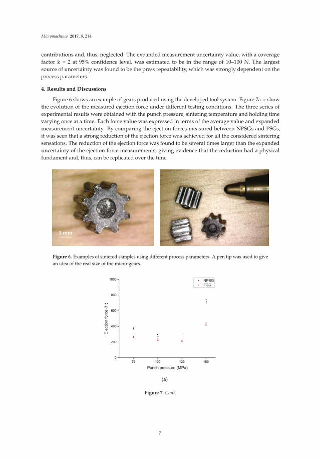
Figure 6 shows an example of gears produced using the developed tool system. Figure 7a–c showthe evolution of the measured ejection force under different testing conditions. The three series ofexperimental results were obtained with the punch pressure, sintering temperature and holding timevarying once at a time. Each force value was expressed in terms of the average value and expandedmeasurement uncertainty. By comparing the ejection forces measured between NPSGs and PSGs,it was seen that a strong reduction of the ejection force was achieved for all the considered sinteringsensations. The reduction of the ejection force was found to be several times larger than the expandeduncertainty of the ejection force measurements, giving evidence that the reduction had a physicalfundament and, thus, can be replicated over the time.
1 mm
Figure 6. Examples of sintered samples using different process parameters. A pen tip was used to givean idea of the real size of the micro-gears.
(a)
Figure 7. Cont.
7
Micromachines 2017, 8, 214
(b)
(c)
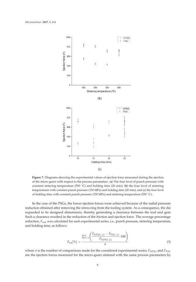
Figure 7. Diagrams showing the experimental values of ejection force measured during the ejectionof the micro-gears with respect to the process parameters. (a) The four level of punch pressure withconstant sintering temperature (550 ◦C) and holding time (20 min); (b) the four level of sinteringtemperatures with constant punch pressure (150 MPa) and holding time (20 min); and (c) the four levelof holding time with constant punch pressure (150 MPa) and sintering temperature (550 ◦C).
In the case of the PSGs, the lower ejection forces were achieved because of the radial pressurereduction obtained after removing the stress-ring from the tooling system. As a consequence, the dieexpanded to its designed dimensions, thereby generating a clearance between the tool and gear.Such a clearance resulted in the reduction of the friction and ejection force. The average percentagereduction, Fred, was calculated for each experimental series, i.e., punch pressure, sintering temperature,and holding time, as follows:
Fred[%] =
∑ni=1
(
FNPSG (i) − FPSG (i)
FNPSG (i)·100
)
n(3)
where n is the number of comparisons made for the considered experimental series; FNPSG and FPSG
are the ejection forces measured for the micro-gears sintered with the same process parameters by
8

Micromachines 2017, 8, 214
using a configuration without and with pre-stress, respectively. A summary of the average resultsfor each experimental series was collected in Table 2. The holding time series showed a reductionof the advantage of the pre-stress as the holding time increased. The longer holding times were,the larger the ejection forces. Such a finding can be due to the fact that longer holding times increasedthe adhesion of a gear to the die walls, resulting in stronger interactions between the surfaces incontact. A similar percentage force reduction was observed by varying either the punch pressure orthe sintering temperature.
Table 2. Average ejection force reduction during the ejection as a function of the process parameters.
Punch Pressure Sintering Temperature Holding Time
−27% −33% −50%
4.1. Visual Inspection of Micro-Gears Using an Optical Microscope
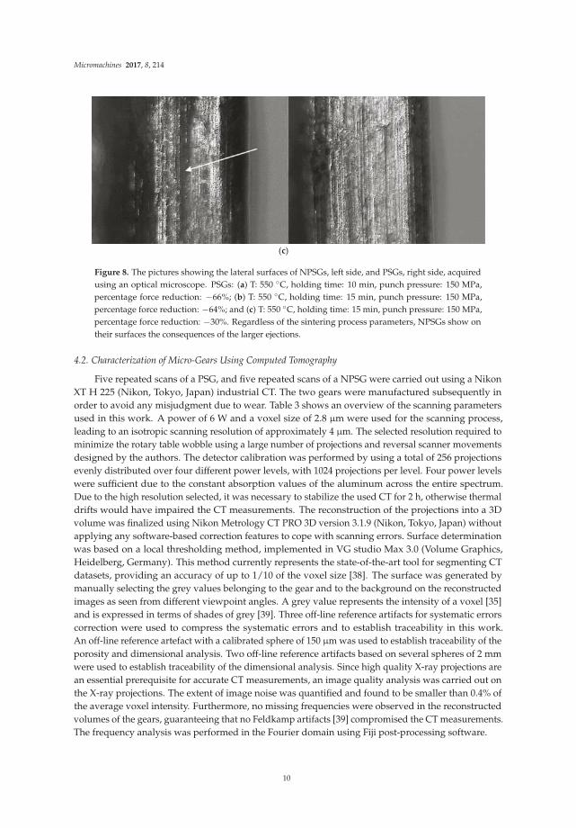
Figure 8 shows a collection of pictures of the gears sintered in the present work. PSGs did notshow any ploughing effect compared to NPSGs where such effect was well visible, as shown in thefigure using arrows. Ploughing was caused by asperities of a tool material metal penetrating into agear material, which was the softer one. Although it may be deducted that the new developed toolsystem increased the uniformity of the surface of the gears, the visual inspection did not give sufficientevidences to make a definitive statement. As a consequence, a quantitative analysis was carried outusing computed tomography.
(a)
(b)
Figure 8. Cont.
9
Micromachines 2017, 8, 214
(c)
Figure 8. The pictures showing the lateral surfaces of NPSGs, left side, and PSGs, right side, acquiredusing an optical microscope. PSGs: (a) T: 550 ◦C, holding time: 10 min, punch pressure: 150 MPa,percentage force reduction: −66%; (b) T: 550 ◦C, holding time: 15 min, punch pressure: 150 MPa,percentage force reduction: −64%; and (c) T: 550 ◦C, holding time: 15 min, punch pressure: 150 MPa,percentage force reduction: −30%. Regardless of the sintering process parameters, NPSGs show ontheir surfaces the consequences of the larger ejections.
4.2. Characterization of Micro-Gears Using Computed Tomography
Five repeated scans of a PSG, and five repeated scans of a NPSG were carried out using a NikonXT H 225 (Nikon, Tokyo, Japan) industrial CT. The two gears were manufactured subsequently inorder to avoid any misjudgment due to wear. Table 3 shows an overview of the scanning parametersused in this work. A power of 6 W and a voxel size of 2.8 µm were used for the scanning process,leading to an isotropic scanning resolution of approximately 4 µm. The selected resolution required tominimize the rotary table wobble using a large number of projections and reversal scanner movementsdesigned by the authors. The detector calibration was performed by using a total of 256 projectionsevenly distributed over four different power levels, with 1024 projections per level. Four power levelswere sufficient due to the constant absorption values of the aluminum across the entire spectrum.Due to the high resolution selected, it was necessary to stabilize the used CT for 2 h, otherwise thermaldrifts would have impaired the CT measurements. The reconstruction of the projections into a 3Dvolume was finalized using Nikon Metrology CT PRO 3D version 3.1.9 (Nikon, Tokyo, Japan) withoutapplying any software-based correction features to cope with scanning errors. Surface determinationwas based on a local thresholding method, implemented in VG studio Max 3.0 (Volume Graphics,Heidelberg, Germany). This method currently represents the state-of-the-art tool for segmenting CTdatasets, providing an accuracy of up to 1/10 of the voxel size [38]. The surface was generated bymanually selecting the grey values belonging to the gear and to the background on the reconstructedimages as seen from different viewpoint angles. A grey value represents the intensity of a voxel [35]and is expressed in terms of shades of grey [39]. Three off-line reference artifacts for systematic errorscorrection were used to compress the systematic errors and to establish traceability in this work.An off-line reference artefact with a calibrated sphere of 150 µm was used to establish traceability of theporosity and dimensional analysis. Two off-line reference artifacts based on several spheres of 2 mmwere used to establish traceability of the dimensional analysis. Since high quality X-ray projections arean essential prerequisite for accurate CT measurements, an image quality analysis was carried out onthe X-ray projections. The extent of image noise was quantified and found to be smaller than 0.4% ofthe average voxel intensity. Furthermore, no missing frequencies were observed in the reconstructedvolumes of the gears, guaranteeing that no Feldkamp artifacts [39] compromised the CT measurements.The frequency analysis was performed in the Fourier domain using Fiji post-processing software.
10

Micromachines 2017, 8, 214
Table 3. Overview of the scanning parameters used in this work.
Parameter Unit Value
X-ray tube voltage kV 130X-ray tube current µA 50
Corrected voxel size µm 2.8Magnification factor - 60
No. of projections - 2000No. of image per projection - 2
Integration time s 0.5Scanning time min 34
The porosity analysis was performed using two representative 3D volumes, one volume pergear, to minimize the impact of external influences such as dust, image noise, and lubricant.The representative 3D volumes were set to enclose approximately 90% of the total volume of eachgear. It was, therefore, assumed that any result obtained from the inspection of the two volumes wasrepresentative of the two entire gears. By using the Procedure for Uncertainty MAnagement (PUMA)method [37], the expanded measurement uncertainty, at 95% confidence level, for the porosity analysiswas estimated to be equal to ±0.01 mm3. The expanded measurement uncertainty was based on thefollowing uncertainty contributions: (i) the uncertainty from the calibration certificates of the off-linereference artefact; (ii) the uncertainty from the measurement repeatability; and (iii) the uncertaintyarising from the image noise. All the uncertainty contributions were based on Type B evaluations [37].The image noise contributed 60% of the expanded measurement uncertainty. Figure 9 shows thespatial porosity distribution for the two gears inspected using CT. The porosity fraction was quantifiedto be 0.03 ± 0.01% and 0.05 ± 0.01% of the representative volume for PSG and NPSG, respectively.By performing a t-test [40], it was found that the two porosity distributions can be assumed to bestatistically different, leading to a conclusion that the pre-stress increased the compactness of thepowder of which the gears were composed. The t-test was conducted at the 95% confidence level andtook into account the measurement uncertainty of the porosity fractions. It was also observed that thepores were found to be distributed within the volumes of both selected gears in a different fashion.PSG showed a uniform porosity within the inspected volume, whereas NPSG did not. As a generalconclusion, the use of pre-stress reduced the gear porosity by 40% and allowed the achievement ofa more uniform spatial distribution of the pores in the gear.
(a) (b)
Figure 9. Volume pore distributions for (a) NPSG and (b) PSG. Deviation range from 0 to 0.00009 mm3.
11

Micromachines 2017, 8, 214
The dimensional analysis of the gears was based on the actual-to-nominal comparison tool [40].The use of the actual-to-nominal comparison allows the quantification of the deviation of each surfacepoint of an object compared to its CAD file [36]. An actual-to-nominal comparison simplifies themeasurement procedures compared to other approaches involving primitive features [36]. By using thePUMA method [37], the expanded measurement uncertainty per voxel was calculated, making eachpoint of an actual-to-nominal comparison traceable to the meter. The measurement uncertainty wasbased on the following uncertainty contributions: (i) the uncertainty from the calibration certificatesof the two used off-line reference artifacts; (ii) the uncertainty from the measurement repeatability;(iii) the uncertainty arising from the image noise; and (iv) uncertainty from the post-processingactivities. The expanded measurement uncertainty was found to be 0.003 mm for all the voxels of thereconstructed volumes. A single uncertainty value was sufficient in this case due to the followingfavorable conditions: (i) no gear movements occurred during scanning, establishing that no localreconstruction errors occurred; (ii) the absence of material-related image artifacts, ensuring thatX-rays were well modelled during reconstruction at any voxel; (iii) the axial symmetry of the gears,making sure that scatter and the X-ray absorption coefficient did not change locally. The measurementuncertainty per voxel represents a source of novelty, paving the way for 3D measurement uncertaintyestimations. Figure 10 shows the two actual-to-nominal comparisons for the two gears with thedeviation range and colors. It can be seen from the figures that the two gears appeared to be extremelydifferent, with PSG having the higher fidelity to the CAD file. PSG showed 95% of its surface liedwithin ±0.009 mm, whereas PSG showed that 95% of its surface lies within ±0.040 mm. By usinga t-test [40], it was confirmed that the two fidelity values were statistically different. As a generalconclusion, the adoption of a pre-stress value can improve the dimensional accuracy of gear by morethan 75% compared to gears produced without pre-stress.
(a)
(b)
Figure 10. Actual-to-nominal comparison for (a) NPSG and (b) PSG. Deviation range ±0.03 mm.
12
Micromachines 2017, 8, 214
5. Conclusions
This paper has presented the development of a pre-stressed tool system for the manufacture ofmicro gears made of aluminum [32]. The developed pre-stressed tool system included a stress-ringand worked according to HIP, thereby reducing the sintering time compared to conventional sintering.Fourteen gears were produced using the pre-stressed tool system and then compared to another14 gears produced after removing the stress-ring. All the gears were manufactured in an environmentkept at of 21 ± 1 ◦C and using different combinations of punch pressure, sintering temperature,and holding time. By using the newly-developed pre-stressed tool system, a reduction in the ejectionforce of up to 50% was observed. The magnitude of the ejection force reduction was found to be largerthan the ejection force measurement uncertainties, giving evidence that such results had a physicalexplanation and, thus, can be replicated over time. Visual inspections, carried out using an opticalmicroscope, showed a reduced frictional interaction on the lateral surface of the micro-gears producedby using a pre-stressed tool system. Furthermore, CT measurements documented that the new toolsystem reduced the porosity in the gear by 40% and improved the dimensional fidelity to CAD bymore than 75% compared to gears produced without pre-stress. Finally, the paper has also introducedthe concept of CT measurement uncertainty per voxel, as well as proved the applicability of CT tomicro-manufacturing with expanded uncertainties of a few microns.
Acknowledgments: This research work was undertaken in the context of MICROMAN project (“Process Fingerprintfor Zerodefect Net-shape MICROMANufacturing”, http://www.microman.mek.dtu.dk/). MICROMAN isa European Training Network supported by Horizon 2020, the EU Framework Programme for Research andInnovation (Project ID: 674801). The first author would also like to thank IPU and Micro-FAST [41] for thepossibility to carry out experiments and for funding tools and dissemination activities related to this project.Moreover, special thanks go to Mogens Arentoft for his supervision and suggestions during the initial period of thisresearch. Finally, special thanks go to the Imaging Industry Centre at DTU for making the CT scanner available.
Author Contributions: Emanuele Cannella designed the tools, operated the experiments, analyzed the results andwrote the paper. Emil Krabbe Nielsen designed the micro-gear shape, supported the experiments, and reviewedand edited the paper. Alessandro Stolfi performed all the CT measurements shown in this work, and reviewedand edited the paper.
Conflicts of Interest: The authors declare no conflict of interest.
References
1. Castro, R.H.R. Overview of Conventional Sintering. In Sintering; Castro, R.H.R., van Benthem, K., Eds.;
Springer: Berlin, Germany, 2013; Volume 35, pp. 1–16.
2. Groza, J.R.; Zavaliangos, A. Nanostructured bulk solids by field activated sintering. Rev. Adv. Mater. Sci.
2003, 5, 24–33.
3. Wang, G.P.; Liu, W.Q.; Huang, Y.L.; Ma, S.C.; Zhong, Z.C. Effects of sintering temperature on the mechanical
properties of sintered NdFeB permanent magnets prepared by spark plasma sintering. J. Magn. Magn. Mater.
2014, 349, 1–4. [CrossRef]
4. Garay, J.E. Current-Activated, Pressure-Assisted Densification of Materials. Annu. Rev. Mater. Res. 2010, 40,
445–468. [CrossRef]
5. Guillon, O.; Gonzalez-Julian, J.; Dargatz, B.; Kessel, T.; Schierning, G.; Rathel, J.; Herrmann, M. Field-assisted
sintering technology/spark plasma sintering: Mechanisms, materials, and technology developments.
Adv. Eng. Mater. 2014, 16, 830–849. [CrossRef]
6. Li, W.; Olevsky, E.A.; McKittrick, J.; Maximenko, A.L.; German, R.M. Densification mechanisms of spark
plasma sintering: Multi-step pressure dilatometry. J. Mater. Sci. 2012, 47, 7036–7046. [CrossRef]
7. Akarachkin, S.A.; Ivashutenko, A.S.; Martyushev, N.V. Activation of mass transfer processes at spark plasma
sintering of zirconium dioxide. IOP Conf. Ser. Mater. Sci. Eng. 2016, 124, 12042. [CrossRef]
8. Zhao, J.; Qin, Y.; Huang, K.; Hijji, H. Forming of micro-components by electrical-field activated sintering.
MATEC Web Conf. 2015, 21. [CrossRef]
9. Orrù, R.; Licheri, R.; Locci, A.M.; Cincotti, A.; Cao, G. Consolidation/synthesis of materials by electric
current activated/assisted sintering. Mater. Sci. Eng. R Rep. 2009, 63, 127–287. [CrossRef]
13

Micromachines 2017, 8, 214
10. Munir, Z.A.; Quach, D.V.; Ohyanagi, M. Electric current activation of sintering: A review of the pulsed
electric current sintering process. J. Am. Ceram. Soc. 2011, 94, 1–19. [CrossRef]
11. Delaizir, G.; Bernard-Granger, G.; Monnier, J.; Grodzki, R.; Kim-Hak, O.; Szkutnik, P.D.; Soulier, M.;
Saunier, S.; Goeuriot, D.; Rouleau, O.; et al. A comparative study of Spark Plasma Sintering (SPS),
Hot Isostatic Pressing (HIP) and microwaves sintering techniques on p-type Bi2Te3 thermoelectric properties.
Mater. Res. Bull. 2012, 47, 1954–1960. [CrossRef]
12. Giuntini, D.; Olevsky, E.A.; Garcia-Cardona, C.; Maximenko, A.L.; Yurlova, M.S.; Haines, C.D.; Martin, D.G.;
Kapoor, D. Localized overheating phenomena and optimization of spark-plasma sintering tooling design.
Materials 2013, 6, 2612–2632. [CrossRef]
13. Chawake, N.; Pinto, L.D.; Srivastav, A.K.; Akkiraju, K.; Murty, B.S.; Kottada, R.S. On Joule heating during
spark plasma sintering of metal powders. Scr. Mater. 2014, 93, 52–55. [CrossRef]
14. Long, W.M. Radial pressures in powder compaction. Powder Metall. 1960, 6, 73–86. [CrossRef]
15. Bockstiegel, G. The Porosity-Pressure Curve and its Relation to the Size Distribution of Pores in Iron Powder
Compacts. In Proceedings of the 1965 International Powder Metallurgy Conference, New York, NY, USA,
14–17 June 1965.
16. Höganäs AB. Production of Sintered Components. Available online: https://www.hoganas.com/
globalassets/media/sharepoint-documents/HandbooksAllDocuments/Handbook2_Production_of_
Sintered_Components_December_2013_0675HOG_interactive.pdf (accessed on 5 June 2017).
17. Rahman, M.M.; Nor, S.S.M. An experimental investigation of metal powder compaction at elevated
temperature. Mech. Mater. 2009, 41, 553–560. [CrossRef]
18. Enneti, R.K.; Lusin, A.; Kumar, S.; German, R.M.; Atre, S.V. Effects of lubricant on green strength,
compressibility and ejection of parts in die compaction process. Powder Technol. 2013, 233, 22–29. [CrossRef]
19. Li, Y.Y.; Ngai, T.L.; Zhang, D.T.; Long, Y.; Xia, W. Effect of die wall lubrication on warm compaction powder
metallurgy. J. Mater. Process. Technol. 2002, 129, 354–358. [CrossRef]
20. Luo, S.D.; Yang, Y.F.; Schaffer, G.B.; Qian, M. Warm die compaction and sintering of titanium and titanium
alloy powders. J. Mater. Process. Technol. 2014, 214, 660–666. [CrossRef]
21. Chen, P.; Kim, G.-Y.; Ni, J. Investigations in the compaction and sintering of large ceramic parts. J. Mater.
Process. Technol. 2007, 190, 243–250. [CrossRef]
22. Andresen, H.; Lund, E. Tooling Solutions for Cold and Warm Forging Applications for Automotive and Other
Segments. Available online: http://www.istma.org/istma-world/ISTMA_Conferencehall/uddeholm2008/
Tooling%20solutions%20for%20cold%20and%20warm%20forging_Erik%20Lund_Henrik%20Andresen.
pdf (accessed on 5 June 2017).
23. Garner, S.; Ruiz, E.; Strong, J.; Zavaliangos, A. Mechanisms of crack formation in die compacted powders
during unloading and ejection: An experimental and modeling comparison between standard straight and
tapered dies. Powder Technol. 2014, 264, 114–127. [CrossRef]
24. Armentani, E.; Bocchini, G.F.; Cricrì, G. Doubly shrink fitted dies: Optimisation by analytical and FEM
calculations. Powder Metall. 2012, 55, 130–141. [CrossRef]
25. Koç, M.; Arslan, M.A. Design and finite element analysis of innovative tooling elements (stress pins) to
prolong die life and improve dimensional tolerances in precision forming processes. J. Mater. Process. Technol.
2003, 142, 773–785. [CrossRef]
26. Groenbaek, J.; Nielsen, E.R. Stripwound containers for combined radial and axial prestressing. J. Mater.
Process. Technol. 1997, 71, 30–35. [CrossRef]
27. Pan, W.; Qin, Y.; Law, F.; Ma, Y.; Brockett, A.; Juster, N. Feasibility study and tool design of using shape
memory alloy as tool-structural elements for forming-error compensation in microforming. Int. J. Adv.
Manuf. Technol. 2008, 38, 393–401. [CrossRef]
28. Qin, Y. Forming-tool design innovation and intelligent tool-structure/system concepts. Int. J. Mach.
Tools Manuf. 2006, 46, 1253–1260. [CrossRef]
29. Fu, M.W.; Chan, W.L. Micro-Scaled Products Development via Microforming; Fu, M.W., Chan, W.L., Eds.;
Springer: Berlin, Germany, 2014; ISBN 9781447163268.
30. Ghassemali, E.; Tan, M.J.; Jarfors, A.E.W.; Lim, S.C.V. Progressive microforming process: Towards the mass
production of micro-parts using sheet metal. Int. J. Adv. Manuf. Technol. 2013, 66, 611–621. [CrossRef]
31. Johnson, D.; Martynov, V.; Gupta, V. Applications of shape memory alloys: Advantages, disadvantages,
and limitations. Proc. SPIE 2001, 4557, 341–351. [CrossRef]
14

Micromachines 2017, 8, 214
32. Cannella, E.; Nielsen, E.K.; Arentoft, M. Ejection force analysis of sintered aluminium micro gears using
a shrink-fit die principle. In Proceedings of the 11th International Conference on Multi-Material Micro
Manufacture (4M2016): Co-organised with 10th International Workshop on Microfactories (IWMF2016),
Kgs. Lyngby, Denmark, 13–15 September 2016; pp. 41–44.
33. Noveanu, D. Researches concerning a new method for obtaining spur gears by metal powder compaction in
elastic dies. Metalurgia 2013, 65, 35–39.
34. Atzori, B. Gusci spessi. In Appunti di Costruzione di Macchine; Libreria Cortina: Padova, Italy, 2001;
pp. 262–281.
35. Kruth, J.P.; Bartscher, M.; Carmignato, S.; Schmitt, R.; De Chiffre, L.; Weckenmann, A. Computed tomography
for dimensional metrology. CIRP Ann. Manuf. Technol. 2011, 60, 821–842. [CrossRef]
36. De Chiffre, L.; Carmignato, S.; Kruth, J.P.; Schmitt, R.; Weckenmann, A. Industrial applications of computed
tomography. CIRP Ann. Manuf. Technol. 2014, 63, 655–677. [CrossRef]
37. Geometrical Product Specifications (GPS)—Inspection by Measurement of Workpieces and Measuring Equipment—Part 2:
Guidance for the Estimation of Uncertainty in GPS Measurement, in Calibration of Measuring Equipment and in Product;
ISO 14253-2:2011; British Standards Institute: London, UK, 2011.
38. Müller, P. Coordinate Metrology by Traceable Computed Tomography; Technical University of Denmark (DTU):
Kgs. Lyngby, Denmark, 2013.
39. Stolfi, A. Integrated Quality Control of Precision Assemblies Using Computed Tomography. Ph.D. Thesis,
Technical University of Denmark (DTU), Kgs. Lyngby, Denmark, 2017.
40. Witt, P.L.; McGrain, P. Comparing two sample means t tests. Phys. Ther. 1985, 65, 1730–1733. [CrossRef]
[PubMed]
41. MICRO-FAST. Available online: www.micro-fast.eu (accessed on 5 June 2017).
© 2017 by the authors. Licensee MDPI, Basel, Switzerland. This article is an open access
article distributed under the terms and conditions of the Creative Commons Attribution
(CC BY) license (http://creativecommons.org/licenses/by/4.0/).
15
micromachines
Article
Rapid Fabrication of Disposable Micromixing ArraysUsing Xurography and Laser Ablation
J. Israel Martínez-López *, H.A. Betancourt, Erika García-López, Ciro A. Rodriguez
and Hector R. Siller
Tecnológico de Monterrey, Eugenio Garza Sada 2501 Sur, 64849 Monterrey, NL, Mexico;[email protected] (H.A.B.); [email protected] (E.G.-L.); [email protected] (C.A.R.);[email protected] (H.R.S.)* Correspondence: [email protected]; Tel.: +52-818-358-2000
Academic Editors: Guido Tosello, Hans Nørgaard Hansen and Nam-Trung NguyenReceived: 28 February 2017; Accepted: 28 April 2017; Published: 4 May 2017
Abstract: We assessed xurography and laser ablation for the manufacture of passive micromixersarrays to explore the scalability of unconventional manufacture technologies that could beimplemented under the restrictions of the Point of Care for developing countries. In this work,we present a novel split-and-recombine (SAR) array design adapted for interfacing standardizeddispensing (handheld micropipette) and sampling (microplate reader) equipment. The design waspatterned and sealed from A4 sized vinyl sheets (polyvinyl chloride), employing low-cost disposablematerials. Manufacture was evaluated measuring the dimensional error with stereoscopic and confocalmicroscopy. The micromixing efficiency was estimated using a machine vision system for passivedriven infusion provided by micropippetting samples of dye and water. It was possible to employrapid fabrication based on xurography to develop a four channel asymmetric split-and-recombine(ASAR) micromixer with mixing efficiencies ranging from 43% to 65%.
Keywords: micromixing; split and recombine; rapid manufacture; xurography; laser ablation
1. Introduction
The development and spread of advanced diagnostic devices based on microfluidic technologycan be a key strategy element to tackle a wide variety of infectious diseases such as AIDS, tuberculosis(TB) or malaria. Despite the availability of diagnostics and solutions for these diseases, every year about15 million people die from these diseases [1]. Academics have proposed a wide variety of devicesbuilt on advanced manufacturing, electromechanical sensors and actuators, and Information andCommunications Technologies (ICT) to treat patients outside the boundaries of a hospital. A significantportion of these devices, gadgets, and systems had been conceived to serve in the Point of Care (POC).The approach to bringing healthcare closer to the patients is inherently well encompassed withtechnologies that enable the miniaturization of established diagnostics, treatment, and monitoringillness. In developing countries, mobility is an asset that can enhance aid by providing closer access toremote areas, treating illnesses at earlier stages, and deterring the spread of infectious diseases.
The World Health Organization (WHO) has resumed the requirements of the in-field solutionsunder the acronym “ASSURED”, which stands for affordable, sensitive, specific, user-friendly, rapidand robust, equipment-free or minimal equipment, and deliverable to end-users. The design andmanufacture of POC devices carries added demanding development requirements. This equipmentshould remain functional in its main purpose reliably under the constraints of being low-cost,the absence of trained staff, lack of electricity, poorly equipped laboratory facilities, and limitedaccess to refrigeration and storage [2,3]. Studies evaluating the performance of POC prognosis haveshown that end-users (typically remote health workers or volunteers) are affected by some factors,
Micromachines 2017, 8, 144 16 www.mdpi.com/journal/micromachines
Micromachines 2017, 8, 144
including manual dexterity, visual acuity, and available lighting during testing. Micropipette orother standardized methods for sample management and transfer can support a more reliable andhigh-throughput capable device operation [4,5].
Despite the copious amount of research in the design and operation of micromixers, researchregarding manufacture technology towards implementation beyond academic environments is limited.Microfabrication-based on the photolithographic processes of polymers is the most common approachemployed [6]. Typically, this implies procedures that require supervision by specialized personnelunder laboratory facilities (i.e., spin coaters, ovens, plasma treatment, hot plates) and requires thesupply of resins for the development of structures within the finesse in the micrometric scale. Thesespecimen can then be used as sample devices or employed to replicate them through casting, stamping,or injection molding. Polydimethylsiloxane (PDMS) is the most popular elastomer due the ability tocast with nanometric resolution and to be relatively inexpensive and because it can be irreversiblybonded to other materials such as glass or other polymeric films [7,8].
In rapid fabrication manufacturing techniques, devices are fabricated faster than conventionalmanufacturing processes. While some of these methodologies were originally conceived solely forproducing one or few samples within some surface or structural quality limitations, now it is possibleto find cases where these techniques have evolved into the production of components that could notbe made otherwise [9]. The incorporation of rapid fabrication technology for microfluidic devicesis a growing trend among researchers, but it has not yet been fully developed [10]. 3D printing hasraised much awareness among academics and media because it allows devices to be manufacturedon-demand with ease and quickness for medical applications [11] of microfluidic devices [12].
Compared to other rapid fabrication technologies such as fused deposition modeling (FDM) orstereolithography (SL), technology that relies on processing thin-films rolls is typically more affordableand can be transported more easily than liquid-based reagents like PDMS or the resins used for theprocesses mentioned above. The roll to roll hot embossing process is a recent advancement in micro hotembossing processes and is capable of continuously fabricating micro/nano structures on the polymerwith high efficiency and high throughput [13,14]. High volume fabrication employing manufacturebased on processing polymer on rolls has been used successfully for pinched flow fractionation oncellulose acetate [13]. Another group developed an electrophoresis chip for the detection of antibioticresistance bacteria by feeding a thermoplastic foil through a hot embossing cylinder [15]. Senkbeil et al.have altered the rheological behavior of the resin system to produce capillary electrophoresis chips.
Xurography is a rapid manufacture technology that originated from the adaptation of equipmentintended for advertisement used for the development of microfluidic systems. It relies on the patterningand removal of thin-films materials using a blade tracing a design [16,17]. Originally, around a decadeago, the major advantage was the simplicity and quickness in operation; nowadays, the cost reductionin these equipment from the original 4000 USD to 200 USD has accentuated the price-value ratioadvantage of this technique compared to more conventional approaches. For example, Silhouette [18]and Cricut [19] are two providers that offer desktop sized cutting equipment designed for homeuse with a starting price of 200 USD for processing standardized A4 sheets with comparable cuttingperformance to more expensive equipment.
Another technique used for manufacturing microdevices from thin layers of materials formattedas rolls is laser ablation. Some research has been developed widely in PDMS [20], glass [21,22], cyclicolefin copolymer (COP) [23], and polymethyl methacrylate (PMMA) [24,25] materials with a variety ofapplications in lab on a chip field. These microdevices have been processed using an ultra short pulsedlaser (e.g., femtosecond and picosecond pulse durations), which results in a promising techniquein micromachining that relies on design flexibility, precision, and productivity. Laser ablation formicrodevices is performed through the interaction between laser energy and the material, where themain parameters are wavelength and pulse duration. Therefore a focused volume absorbs laser energy,which allows a localized machining, while the rest of the sample results are unaffected [26]. Among thelaser ablation equipment, engravers are a subset of machines suited for cutting non-metallic materials.
17
Micromachines 2017, 8, 144
Prices can vary widely depending on the type of laser, work area, and features from roughly 8000 USDto 5000 USD. Recently there have been some efforts funded by crowdfunded projects to commercializeprototypes focused on hobbyists with lower price baselines and added features [27,28]. However thesealternatives remain above 500 USD and are still in development.
One of the desirable operations that a POC device must perform is micromixing since devices atthe micrometric scale tend naturally to operate on a laminar flow regime. Under that condition, thehomogenization and reaction of reagents tend to be slow or require systems with large characteristiclength to function properly [29,30]. Rather than perform micromixing by a supplementary force,passive micromixing depends on geometrical features along the flow chamber. For example, slantedgrooved [31,32] and staggered herringbone [33] micromixers induce homogenization by creating secondaryflows using obstacles or other complex features along the flow chamber. These designs are typicallyhighly efficient in the task of mixing but also require expensive multi-layer manufacture technology.
A widely studied example of a passive micromixer is the T-mixer. In this simple design, twoseparate fluids are brought into contact from opposite directions and then leave through a channel thatis perpendicular to the inlet channels [24]. The performance tends to be low as the mixing occurs onlyproximate to the junction. A more recent methodology, SAR or ASAR micromixers force this contactby repeatedly putting together the streams from the inputs and hence increasing the interfacial area ofthe streams. Recent research had employed the principle of the T-mixer by splitting and recombiningstreams iteratively with more complex geometry as rhombic [34,35], modified Tesla [36–38], or curvebased [39–41] and shapes based setups. Table 1 represents the recent development and the manufacturemethodologies and some micromixers channels per device (N) for in-plane micromixers prior tothis work. It is noticeable that, before the present work, Chung et al. [42] used a laser as part of amanufacturing process, but this was not done with consideration of either POC or rapid manufacturing.The authors have not found previous work from other research groups on the development ofinterfacing a micromixer with standardized sample management equipment, neither have they founddeported efforts to develop full-sized arrays.
Table 1. Manufacture methodologies for in-plane micromixers.
Work Reference Manufacture Methodology N winput
Hong et al. (2004) [37]Molding (nickel-SU-8), photolitography, hotembossing, drilling, thermal bonding
1 200 µm
Sudarsan & Ugaz (2006) [39] Circuit printing, etching, heat treatment 1 150 µm
Chung & Shi (2007) [34]Lithography, micro-molding, oxygen plasma treatmentbonding, mechanical punching
1 500 µm
Chung et al. (2009) [42]Laser machining, PDMS casting from PMMA, thermaland oxygen plasma bonding, mechanical punching
1 500 µm
Ansari et al. (2010) [40]SU-8 photolithography over a silicon wafer, PDMSmolding, mechanical punching
1 300 µm
Scherr et al. (2012) [43]SU-8 photolithography, PDMS molding, plasmacleaning, mechanical punching
1 30–200 µm
Li et al. (2013) [44] PDMS molding 1 300 µm
Martínez-López et al. (2016) [10] Xurography of PVC and manual lamination 1 750 µm
To address these restrictions in the deployment of a particular type of microfluidic device (SAR)micromixer, we have recently developed a methodology to produce single devices from scratch totesting without the requirement of ancillary laboratory equipment [10,45]. Combining xurographyand lamination offered promissing advantages over conventional manufacture such as flexibility, shortcycle times, and low-cost. However, to deploy micromixers such as POC, it is important to confrontthe scalability of the process to produce massively and reliably these devices in the field.
18
Micromachines 2017, 8, 144
In this work, we present a scaled-up version of a novel split-and-recombine (SAR) array designpresented before by our group [10,45] and adapted to be an interface for a handheld multichannelmicropipette as a step forward to meet the aforementioned criteria. The manufacturability has beenassessed for xurography and laser ablation. A benchmark between these manufacturing processesis relevant as they are the commercially available alternatives for processing thin-films withoutspecialized laboratory equipment.
While the mere availability of POC technologies does not automatically ensure their adoption [46,47],the authors of this article believe that the flexibility of rapid fabrication provided by manufacture basedon polymeric films along high-throughput capabilities can ease the integration of micromixing as part ofmore complex and functional diagnosis, treatment, and monitoring systems. For example, micromixinghas shown potential as a low-cost sensitivity enhancer for biosensing micro-devices [48–50].
2. Materials and Methods
A Graphtec CE5000–60 (Graphtec America, Irvine, CA, USA) high precision cutting plotterand a Telesis EV25DS (Telesis Technologies, Circleville, OH, USA) marking system were used toassess xurography and laser ablation. Standard commercial Arlon vinyl sheets (polyvinyl chloride;Arlon Graphics, Placentia, CA, USA) were used for the manufacturability assessment (this vendorwas selected considering the availability of a worldwide distributor network). Manufacture usingxurography was employed on a testing material with three color variations; gray (GX), orange (OX),and black (BX) using a similar methodology introduced by a previous work for a single micromixerdevice [10,45] and then adapted and employed on materials of the same batch for gray (GL), orange(OL), and black (BL) using ablation. The procedures can be summarized as follows: a microfluidicdevice can be developed by patterning and stacking four layers of materials. A PMMA substrate(Layer 0) provides the mechanical stiffness required for handling the device, a vinyl pattern (Layer 1)forms the flow cell walls, and an acetate sheet (Layer 2) is employed to provide an enclosure ceiling tothe device and provide additional structural support to the (Layer 4) vinyl sheet that seals the deviceand delimits the inlets and outlets. Tables 2 and 3 and Sections 2.1 and 2.2 describe more thoroughlythe setup conditions.
The implementation of the rapid fabrication methodology studied in this article was assessedin the manufacturing process of a passive micromixing following a procedure presented in previouswork [10] and expanded for an array configuration. The implemented design is based on previousresearch [10,40,45] on an unbalanced split and recombine micromixer. Figure 1a,b shows our proposedtesting device setup. A standard 96 microwell microplate (Sigma-Aldrich, Saint Louis, MO, USA) ormicrotiter is used to store samples prior processing. A standard multichannel micropipette (ThermoFischer, Waltham, MA, USA) was used to collect the samples from the microwells to introduce them ina four channel microdevice (I to IV). Figure 1b describes the array configuration: each of the channelsis integrated by two inputs (IA, IB, IC, etc.), a six phase asymmetric split, and a recombine micromixer;whereas the input main channel (winput = 1500 µm) is divided subsequently into a main subchannel(w1 = w3 = w5 = w7 = 1000 µm) and a lesser subchannel (w2 = w4 = w6 = w8 = w10 = w12 = 500 µm).The inputs and outputs of the device (�input = �output) are equally spaced (xd = xm = 9 mm) andshare the same dimension pipette to pipette distance. The overall size of the micromixer array is92 mm × 86.5 mm.
2.1. Xurography Setup
A Graphtec CE5000-60 (Graphtec America, Irvine, CA, USA) high precision cutting plotterwas used to pattern 4500 CalPlus vinyl sheet (Layer 1, Arlon Graphics LLC, Placentia, CA, USA).This equipment has a list price around $2000 USD.
Figure 1b describes the four layers composing the micromixing arrays. Commercial acetate sheetstransparency foils were used to pattern the intermediate layer (Layer 2; 21.59 × 27.94 cm). The thicknessof the acetate sheets was found to be variable among the stock and was examined using confocal
19

Micromachines 2017, 8, 144
microscopy prior experimentation. Devices were sealed using a CalPlus 5000 transparent polymericfilm (Layer 3, Arlon Graphics LLC, Placentia, CA, USA) to the cutting machine software (GraphtecDesign Studio, Graphtec America, Irvine, CA, USA) for patterning Layers 1, 2, and 3. The cutting toolused for this work was a standard carbide cutting tool model CB09U with a cutting diameter of 0.9 mmand a cutting angle of 45◦. Tables 2 and 3 describe the details of the setup conditions for patterningthe materials.
Figure 1. (a) Schematics of standardized handheld multichannel micropipette and microwell plate;(b) four-channel asymmetric split-and-recombine (ASAR) micromixer (two inputs and two outputs)microdevice setup used to evaluate xurography and laser ablation; (c) conforming layers of a microdevice.
Table 2. Setup conditions for laser ablation and xurography.
SetupManufactureTechnology
PatterningMechanism
Patterning Conditions Testing Material
GX,OX,BX
Xurography:Graphtec
CE5000-60
Blade CB09U(45◦)
Fload ≈ 0.8 N,Number of passes = 1
Gray, Orange,Black 4500 CalPlus
GL,OL,FLLaser ablation:Telesis EV25DS
Q-switchedNd: YVO4 laser
Mark speed = 500 mm/min,Frequency = 10 kHz,
Laser power = 22.5 W,Pass number = 10
Gray, Orange,Black 4500 CalPlus
20
Micromachines 2017, 8, 144
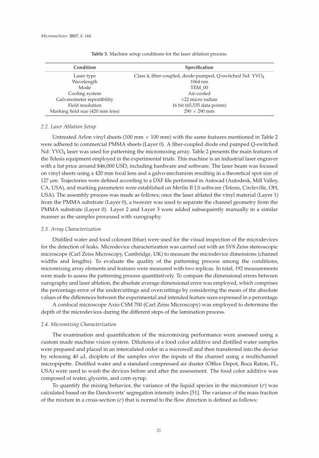
Table 3. Machine setup conditions for the laser ablation process.
Condition Specification
Laser type Class 4, fiber-coupled, diode-pumped, Q-switched Nd: YVO4Wavelength 1064 nm
Mode TEM_00Cooling system Air-cooled
Galvanometer repeatibility <22 micro radianField resolution 16 bit (65,535 data points)
Marking field size (420 mm lens) 290 × 290 mm
2.2. Laser Ablation Setup
Untreated Arlon vinyl sheets (100 mm × 100 mm) with the same features mentioned in Table 2were adhered to commercial PMMA sheets (Layer 0). A fiber-coupled diode end pumped Q-switchedNd: YVO4 laser was used for patterning the micromixing array. Table 2 presents the main features ofthe Telesis equipment employed in the experimental trials. This machine is an industrial laser engraverwith a list price around $46,000 USD, including hardware and software. The laser beam was focusedon vinyl sheets using a 420 mm focal lens and a galvo-mechanism resulting in a theoretical spot size of127 µm. Trajectories were defined according to a DXF file performed in Autocad (Autodesk, Mill Valley,CA, USA), and marking parameters were established on Merlin II LS software (Telesis, Circleville, OH,USA). The assembly process was made as follows; once the laser ablated the vinyl material (Layer 1)from the PMMA substrate (Layer 0), a tweezer was used to separate the channel geometry from thePMMA substrate (Layer 0). Layer 2 and Layer 3 were added subsequently manually in a similarmanner as the samples processed with xurography.
2.3. Array Characterization
Distilled water and food colorant (blue) were used for the visual inspection of the microdevicesfor the detection of leaks. Microdevice characterization was carried out with an SV8 Zeiss stereoscopicmicroscope (Carl Zeiss Microscopy, Cambridge, UK) to measure the microdevice dimensions (channelwidths and lengths). To evaluate the quality of the patterning process among the conditions,micromixing array elements and features were measured with two replicas. In total, 192 measurementswere made to assess the patterning process quantitatively. To compare the dimensional errors betweenxurography and laser ablation, the absolute average dimensional error was employed, which comprisesthe percentage error of the undercuttings and overcuttings by considering the mean of the absolutevalues of the differences between the experimental and intended feature sizes expressed in a percentage.
A confocal microscope Axio CSM 700 (Carl Zeiss Microscopy) was employed to determine thedepth of the microdevices during the different steps of the lamination process.
2.4. Micromixing Characterization
The examination and quantification of the micromixing performance were assessed using acustom made machine vision system. Dilutions of a food color additive and distilled water sampleswere prepared and placed in an intercalated order in a microwell and then transferred into the deviceby releasing 40 µL droplets of the samples over the inputs of the channel using a multichannelmicropipette. Distilled water and a standard compressed air duster (Office Depot, Boca Raton, FL,USA) were used to wash the devices before and after the assessment. The food color additive wascomposed of water, glycerin, and corn syrup.
To quantify the mixing behavior, the variance of the liquid species in the micromixer (σ) wascalculated based on the Danckwerts’ segregation intensity index [51]. The variance of the mass fractionof the mixture in a cross-section (σ) that is normal to the flow direction is defined as follows:
21
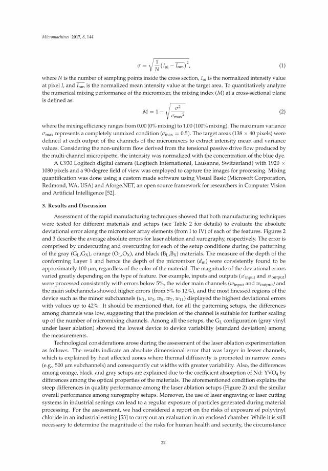
Micromachines 2017, 8, 144
σ =
√
1N
(
Ini − Inm)2
, (1)
where N is the number of sampling points inside the cross section, Ini is the normalized intensity valueat pixel I, and Inm is the normalized mean intensity value at the target area. To quantitatively analyzethe numerical mixing performance of the micromixer, the mixing index (M) at a cross-sectional planeis defined as:
M = 1 −
√
σ2
σmax2 (2)
where the mixing efficiency ranges from 0.00 (0% mixing) to 1.00 (100% mixing). The maximum varianceσmax represents a completely unmixed condition (σmax = 0.5). The target areas (138 × 40 pixels) weredefined at each output of the channels of the micromixers to extract intensity mean and variancevalues. Considering the non-uniform flow derived from the tensional passive drive flow produced bythe multi-channel micropipette, the intensity was normalized with the concentration of the blue dye.
A C930 Logitech digital camera (Logitech International, Lausanne, Switzerland) with 1920 ×
1080 pixels and a 90-degree field of view was employed to capture the images for processing. Mixingquantification was done using a custom made software using Visual Basic (Microsoft Corporation,Redmond, WA, USA) and Aforge.NET, an open source framework for researchers in Computer Visionand Artificial Intelligence [52].
3. Results and Discussion
Assessment of the rapid manufacturing techniques showed that both manufacturing techniqueswere tested for different materials and setups (see Table 2 for details) to evaluate the absolutedeviational error along the micromixer array elements (from I to IV) of each of the features. Figures 2and 3 describe the average absolute errors for laser ablation and xurography, respectively. The error iscomprised by undercutting and overcutting for each of the setup conditions during the patterningof the gray (GL,GX), orange (OL,OX), and black (BL,BX) materials. The measure of the depth of theconforming Layer 1 and hence the depth of the micromixer (dm) were consistently found to beapproximately 100 µm, regardless of the color of the material. The magnitude of the deviational errorsvaried greatly depending on the type of feature. For example, inputs and outputs (�input and �output)were processed consistently with errors below 5%, the wider main channels (winput and woutput) andthe main subchannels showed higher errors (from 5% to 12%), and the most finessed regions of thedevice such as the minor subchannels (w1, w3, w5, w7, w11) displayed the highest deviational errorswith values up to 42%. It should be mentioned that, for all the patterning setups, the differencesamong channels was low, suggesting that the precision of the channel is suitable for further scalingup of the number of micromixing channels. Among all the setups, the GL configuration (gray vinylunder laser ablation) showed the lowest device to device variability (standard deviation) amongthe measurements.
Technological considerations arose during the assessment of the laser ablation experimentationas follows. The results indicate an absolute dimensional error that was larger in lesser channels,which is explained by heat affected zones where thermal diffusivity is promoted in narrow zones(e.g., 500 µm subchannels) and consequently cut widths with greater variability. Also, the differencesamong orange, black, and gray setups are explained due to the coefficient absorption of Nd: YVO4 bydifferences among the optical properties of the materials. The aforementioned condition explains thesteep differences in quality performance among the laser ablation setups (Figure 2) and the similaroverall performance among xurography setups. Moreover, the use of laser engraving or laser cuttingsystems in industrial settings can lead to a regular exposure of particles generated during materialprocessing. For the assessment, we had considered a report on the risks of exposure of polyvinylchloride in an industrial setting [53] to carry out an evaluation in an enclosed chamber. While it is stillnecessary to determine the magnitude of the risks for human health and security, the circumstance
22
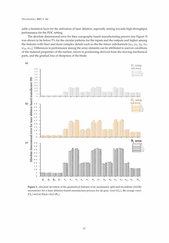
Micromachines 2017, 8, 144
adds a limitation layer for the utilization of laser ablation, especially aiming towards high-throughputperformance for the POC setting.
The absolute dimensional error for then xurography based manufacturing process (see Figure 3)was shown to be below 5% for the circular patterns for the inputs and the outputs and higher amongthe features with finer and more complex details such as the the minor subchannels (w2, w3, w6, w7,w10, w11). Differences in performance among the array elements can be attributed to uneven conditionsof the material properties of the surface, errors in positioning derived from the moving mechanicalparts, and the gradual loss of sharpness of the blade.
Figure 2. Absolute deviation of the geometrical features of an asymmetric split-and-recombine (ASAR)micromixer for a laser ablation-based manufacture process for (a) gray vinyl (GL), (b) orange vinyl(OL) and (c) black vinyl (BL).
23
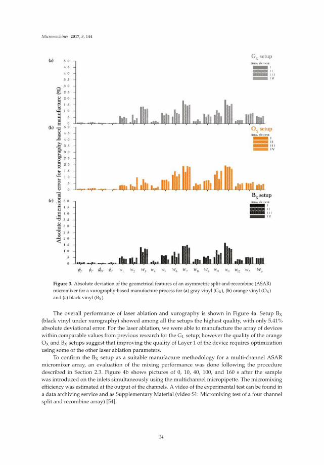
Micromachines 2017, 8, 144
Figure 3. Absolute deviation of the geometrical features of an asymmetric split-and-recombine (ASAR)micromixer for a xurography-based manufacture process for (a) gray vinyl (GX), (b) orange vinyl (OX)and (c) black vinyl (BX).
The overall performance of laser ablation and xurography is shown in Figure 4a. Setup BX
(black vinyl under xurography) showed among all the setups the highest quality, with only 5.41%absolute deviational error. For the laser ablation, we were able to manufacture the array of deviceswithin comparable values from previous research for the GL setup; however the quality of the orangeOX and BX setups suggest that improving the quality of Layer 1 of the device requires optimizationusing some of the other laser ablation parameters.
To confirm the BX setup as a suitable manufacture methodology for a multi-channel ASARmicromixer array, an evaluation of the mixing performance was done following the proceduredescribed in Section 2.3. Figure 4b shows pictures of 0, 10, 40, 100, and 160 s after the samplewas introduced on the inlets simultaneously using the multichannel micropipette. The micromixingefficiency was estimated at the output of the channels. A video of the experimental test can be found ina data archiving service and as Supplementary Material (video S1: Micromixing test of a four channelsplit and recombine array) [54].
24
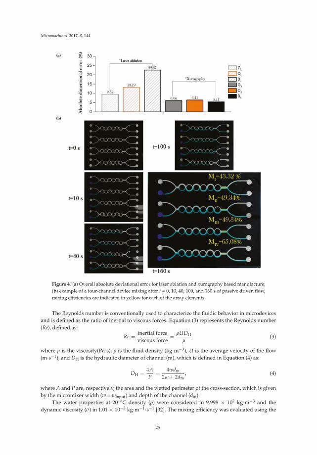
Micromachines 2017, 8, 144
Figure 4. (a) Overall absolute deviational error for laser ablation and xurography based manufacture;(b) example of a four-channel device mixing after t = 0, 10, 40, 100, and 160 s of passive driven flow,mixing efficiencies are indicated in yellow for each of the array elements.
The Reynolds number is conventionally used to characterize the fluidic behavior in microdevicesand is defined as the ratio of inertial to viscous forces. Equation (3) represents the Reynolds number(Re), defined as:
Re =inertial forceviscous force
=ρUDH
µ. (3)
where µ is the viscosity(Pa·s), ρ is the fluid density (kg·m−3), U is the average velocity of the flow(m·s−1), and DH is the hydraulic diameter of channel (m), which is defined in Equation (4) as:
DH =4A
P=
4wdm
2w + 2dm, (4)
where A and P are, respectively, the area and the wetted perimeter of the cross-section, which is givenby the micromixer width (w = winput) and depth of the channel (dm).
The water properties at 20 ◦C density (ρ) were considered in 9.998 × 10² kg·m−3 and thedynamic viscosity (σ) in 1.01 × 10⁻³ kg·m−1
·s−1 [32]. The mixing efficiency was evaluated using the
25
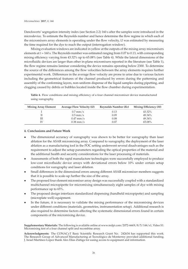
Micromachines 2017, 8, 144
Danckwerts’ segregation intensity index (see Section 2.2) 160 s after the samples were introduced in themicrodevice. To estimate the Reynolds number and hence determine the flow regime in which each ofthe micromixers array elements is operating under the flow velocity, U was estimated by measuringthe time required for the dye to reach the output (interrogation window).
Mixing evaluation windows are indicated in yellow at the outputs of the mixing array micromixerselements at t = 160 s. The Reynolds number was estimated ranging from 0.07 to 0.13, with correspondingmixing efficiency varying from 43.32% up to 65.08% (see Table 4). While the lateral dimensions of themicrofluidic devices are larger than other in-plane micromixers reported in the literature (see Table 1),the flow regime remains laminar considering the device remains operating below 2300. To determinethe source of the differences among the flow velocities between the array elements requires furtherexperimental work. Differences in the average flow velocity are prone to arise due to various factorsincluding the geometrical features of the channel produced by errors during the patterning andassembly of the conforming layers, non-uniform dispense of the liquid samples during pipetting, andclogging caused by debris or bubbles located inside the flow chamber during experimentation.
Table 4. Flow conditions and mixing efficiency of a four channel micromixer device manufacturedusing xurography.
Mixing Array Element Average Flow Velocity (U) Reynolds Number (Re) Mixing Efficiency (M)
I 0.7 mm/s 0.13 43.32%II 0.5 mm/s 0.09 49.34%III 0.47 mm/s 0.08 49.34%IV 0.38 mm/s 0.07 65.08%
4. Conclusions and Future Work
• The dimensional accuracy of xurography was shown to be better for xurography than laserablation for the ASAR micromixing array. Compared to xurography, the deployment of the laserablation as a manufacturing tool in the POC setting underwent several disadvantages such as therequirement to adjust the setup parameters regarding the optical properties of the material andthe additional health and security considerations for the laser processing of materials.
• Assessments of both the rapid manufacture technologies were successfully employed to producelow-cost microfluidic device arrays with deviational errors below 10% under certain setupconditions for xurography and laser ablation.
• Small differences in the dimensional errors among different ASAR micromixer members suggeststhat it is possible to scale-up further the size of the array.
• The proposed four element micromixer array design was successfully coupled with a standardizedmultichannel micropipette for micromixing simultaneously eight samples of dye with mixingperformance up to 65%.
• The proposed design interfaces standardized dispensing (handheld micropipette) and sampling(microplate well) equipment.
• In the future, it is necessary to validate the mixing performance of the micromixing devicesunder different conditions (materials, geometries, instrumentation setup). Additional research isalso required to determine factors affecting the systematic dimensional errors found in certaincomponents of the micromixing device.
Supplementary Materials: The following is available online at www.mdpi.com/2072-666X/8/5/144/s1, Video S1:Micromixing test of a four channel split and recombine array.
Acknowledgments: The CONACyT Basic Scientific Research Grant No. 242634 has supported this work.The Research Group of Advanced Manufacturing at Tecnológico de Monterrey provided additional funding.J. Israel Martínez-López thank Alex Elías Zúñiga for easing access to equipment and information.
26

Micromachines 2017, 8, 144
Author Contributions: J.I.M.L. conceived and designed the micromixer and evaluated the mixing performancedata, he was also responsible of writing major extents of the article. H.A.B. performed the manufacturing processesand collaborated with the mixing characterization. E.G.-L. designed the setup conditions for the laser ablationprocess. J.I.M.L. and H.R.S. contributed insights regarding the assessment analysis. C.A.R. contributed to theanalysis of data and aided in the selection, operation, and performance of the manufacturing technologies.
Conflicts of Interest: The authors declare no conflict of interest.
Abbreviations
The following abbreviations are used in this manuscript:
AIDS Acquired Immune Deficiency SyndromeASAR Asymmetric split and recombinationCAD Computer aided designCOC Cyclic olefin copolymerCOP Cyclic olefin polymerDXF Drawing Interchange FormatEP ElectrophoresisFDM Fused deposition modelingSAR Split and recombineSGM Slanted grooved mixerSHM Staggered herringbone mixerPC PolycarbonatePET Polyethylene terephthalatePETG Polyethylene terephthalate glycolPDMS PolydimethylsiloxanePEEK Polyether ether ketonePMMA Polymethyl methacrylatePOC Point-of-CarePVC Polyvinyl chlorideRGB Red-green-blueSL StereolitographyTB TuberculosisWHO World Health Organization
References
1. Bissonnette, L.; Bergeron, M.G. Diagnosing infections—Current and anticipated technologies for point-of-care
diagnostics and home-based testing. Clin. Microbiol. Infect. 2010, 16, 1044–1053. [CrossRef] [PubMed]
2. Mabey, D.; Peeling, R.W.; Ustianowski, A.; Perkins, M.D. Diagnostics for the developing world. Nat. Rev. Microbiol.
2004, 2, 231–240. [CrossRef] [PubMed]
3. Chin, C.D.; Linder, V.; Sia, S.K. Lab-on-a-chip devices for global health: Past studies and future opportunities.
Lab Chip 2006, 7, 41–57. [CrossRef] [PubMed]
4. Bell, D.; Peeling, R.W. Evaluation of rapid diagnostic tests: Malaria. Nat. Rev. Microbiol. 2006, 4, S34–S38.
[CrossRef] [PubMed]
5. Banoo, S.; Bell, D.; Bossuyt, P.; Herring, A.; Mabey, D.; Poole, F.; Smith, P.G.; Sriram, N.; Wongsrichanalai, C.;
Linke, R.; et al. Evaluation of diagnostic tests for infectious diseases: general principles. Nat. Rev. Microbiol.
2008, 8, S16–S28. [CrossRef] [PubMed]
6. Natarajan, S.; Chang-Yen, D.A.; Gale, B.K. Large-area, high-aspect-ratio SU-8 molds for the fabrication of
PDMS microfluidic devices. J. Micromech. Microeng. 2008, 18, 045021. [CrossRef]
7. McDonald, J.C.; Whitesides, G.M. Poly(dimethylsiloxane) as a material for fabricating microfluidic devices.
Acc. Chem. Res. 2002, 35, 491–499. [CrossRef] [PubMed]
8. Ren, K.; Zhou, J.; Wu, H. Materials for microfluidic chip fabrication. Acc. Chem. Res. 2013, 46, 2396–2406.
[CrossRef] [PubMed]
27

Micromachines 2017, 8, 144
9. Mogi, K.; Sugii, Y.; Yamamoto, T.; Fujii, T. Rapid fabrication technique of nano/microfluidic device with
high mechanical stability utilizing two-step soft lithography. Sens. Actuators B Chem. 2014, 201, 407–412.
[CrossRef]
10. Martínez-López, J.I.; Mojica, M.; Rodríguez, C.A.; Siller, H.R. Xurography as a rapid fabrication alternative
for point-of-care devices: Assessment of passive micromixers. Sensors 2016, 16, 705. [CrossRef] [PubMed]
11. Ventola, C.L. Medical applications for 3D printing: Current and projected uses. Pharm. Ther. 2014, 39, 704–711.
12. Yazdi, A.A.; Popma, A.; Wong, W.; Nguyen, T.; Pan, Y.; Xu, J. 3D printing: An emerging tool for novel
microfluidics and lab-on-a-chip applications. Microfluid. Nanofluid. 2016, 20, 50. [CrossRef]
13. Vig, A.L.; Mäkelä, T.; Majander, P.; Lambertini, V.; Ahopelto, J.; Kristensen, A. Roll-to-roll fabricated
lab-on-a-chip devices. J. Micromech. Microeng. 2011, 21, 035006. [CrossRef]
14. Deng, Y.; Yi, P.; Peng, L.; Lai, X.; Lin, Z. Flow behavior of polymers during the roll-to-roll hot embossing
process. J. Micromech. Microeng. 2015, 25, 065004. [CrossRef]
15. Liedert, R.; Amundsen, L.K.; Hokkanen, A.; Mäki, M.; Aittakorpi, A.; Pakanen, M.; Scherer, J.R.; Mathies, R.A.;
Kurkinen, M.; Uusitalo, S.; et al. Disposable roll-to-roll hot embossed electrophoresis chip for detection of
antibiotic resistance gene mecA in bacteria. Lab Chip 2011, 12, 333–339. [CrossRef] [PubMed]
16. Bartholomeusz, D.A.; Boutte, R.W. Xurography: Rapid prototyping of microstructures using a cutting plotter.
Microelectromech. Syst. J. 2006, 14, 1364–1374. [CrossRef]
17. Treise, I.; Fortner, N.; Shapiro, B.; Hightower, A. Efficient energy based modeling and experimental validation
of liquid filling in planar micro-fluidic components and networks. Lab Chip 2005, 5, 285–297. [CrossRef]
[PubMed]
18. Silhouette America. Available online: https://www.silhouetteamerica.com/ (accessed on 14 April 2017).
19. Cricut. Available online: https://home.cricut.com/ (accessed on 14 April 2017).
20. Huang, H.; Guo, Z. Ultra-short pulsed laser PDMS thin-layer separation and micro-fabrication.
J. Micromech. Microeng. 2009, 19, 055007. [CrossRef]
21. Liao, Y.; Ju, Y.; Zhang, L.; He, F.; Zhang, Q.; Shen, Y.; Chen, D.; Cheng, Y.; Xu, Z.; Sugioka, K.
Three-dimensional microfluidic channel with arbitrary length and configuration fabricated inside glass by
femtosecond laser direct writing. Opt. Lett. 2010, 35, 3225–3227. [CrossRef] [PubMed]
22. Ben-Yakar, A.; Byer, R.L.; Harkin, A.; Ashmore, J.; Stone, H.A.; Shen, M.; Mazur, E. Morphology of
femtosecond-laser-ablated borosilicate glass surfaces. Appl. Phys. Lett. 2003, 83, 3030–3032. [CrossRef]
23. McCann, R.; Bagga, K.; Groarke, R.; Stalcup, A.; Vázquez, M.; Brabazon, D. Microchannel fabrication on
cyclic olefin polymer substrates via 1064 nm Nd:YAG laser ablation. Appl. Surf. Sci. 2016, 387, 603–608.
[CrossRef]
24. Grzybowski, B.A.; Haag, R.; Bowden, N.; Whitesides, G.M. Generation of micrometer-sized patterns for
microanalytical applications using a laser direct-write method and microcontact printing. Anal. Chem. 1998,
70, 4645–4652. [CrossRef]
25. Hong, T.-F.; Ju, W.-J.; Wu, M.-C.; Tai, C.-H.; Tsai, C.-H.; Fu, L.-M. Rapid prototyping of PMMA microfluidic
chips utilizing a CO2 laser. Microfluid. Nanofluid. 2010, 9, 1125–1133. [CrossRef]
26. Malek, C.G.K. Laser processing for bio-microfluidics applications (part II). Anal. Bioanal. Chem. 2006, 385,
1362–1369. [CrossRef] [PubMed]
27. Pinecone Robotics. Available online: http://www.p-robots.com (accessed on 14 April 2017).
28. Mr Beam-Laser Cutting for Everybody. Available online: http://mr-beam.org/#tech (accessed on 14 April 2017).
29. Nguyen, N.-T.; Wu, Z. Micromixers—A review. J. Micromech. Microeng. 2005, 15, R1–R16. [CrossRef]
30. Su, Y.; Chen, G.; Yuan, Q. Ideal micromixing performance in packed microchannels. Chem. Eng. Sci. 2011, 66,
2912–2919. [CrossRef]
31. Schönfeld, F.; Hardt, S. Simulation of helical flows in microchannels. AIChE J. 2004, 50, 771–778. [CrossRef]
32. Du, Y.; Zhang, Z.; Yim, C.; Lin, M.; Cao, X. Evaluation of floor-grooved micromixers using concentration-
channel length profiles. Micromachines 2010, 1, 19–33. [CrossRef]
33. Stroock, A.D.; Dertinger, S.K.W.; Ajdari, A.; Mezic, I.; Stone, H.A.; Whitesides, G.M. Chaotic mixer for
microchannels. Science 2002, 295, 647–651. [CrossRef] [PubMed]
34. Chung, C.K.; Shih, T.R. Effect of geometry on fluid mixing of the rhombic micromixers. Microfluid. Nanofluid.
2007, 4, 419–425. [CrossRef]
35. Hossain, S.; Kim, K.-Y. Mixing analysis of passive micromixer with unbalanced three-split rhombic
sub-channels. Micromachines 2014, 5, 913–928. [CrossRef]
28
Micromachines 2017, 8, 144
36. Hong, C.-C.; Choi, J.-W.; Ahn, C.H. A novel in-plane passive micromixer using coanda effect. In Micro Total
Analysis Systems 2001; Ramsey, J.M., van den Berg, A., Eds.; Springer: Dordrecht, The Netherlands, 2001;
pp. 31–33.
37. Hong, C.-C.; Choi, J.-W.; Ahn, C.H. A novel in-plane passive microfluidic mixer with modified Tesla
structures. Lab Chip 2004, 4, 109–113. [CrossRef] [PubMed]
38. Hossain, S.; Ansari, M.A.; Husain, A.; Kim, K.-Y. Analysis and optimization of a micromixer with a modified
Tesla structure. Chem. Eng. J. 2010, 158, 305–314. [CrossRef]
39. Sudarsan, A.P.; Ugaz, V.M. Fluid mixing in planar spiral microchannels. Lab Chip 2006, 6, 74–82. [CrossRef]
[PubMed]
40. Ansari, M.A.; Kim, K.-Y.; Anwar, K.; Kim, S.M. A novel passive micromixer based on unbalanced splits and
collisions of fluid streams. J. Micromech. Microeng. 2010, 20, 055007. [CrossRef]
41. Ansari, M.A.; Kim, K.-Y. Mixing performance of unbalanced split and recombine micomixers with circular
and rhombic sub-channels. Chem. Eng. J. 2010, 162, 760–767. [CrossRef]
42. Chung, C.K.; Shih, T.R.; Wu, B.H.; Chang, C.K. Design and mixing efficiency of rhombic micromixer with
flat angles. Microsyst. Technol. 2009, 16, 1595–1600. [CrossRef]
43. Scherr, T.; Quitadamo, C.; Tesvich, P.; Park, D.S.-W.; Tiersch, T.; Hayes, D.; Choi, J.-W.; Nandakumar, K.;
Monroe, W.T. A planar microfluidic mixer based on logarithmic spirals. J. Micromech. Microeng. 2012, 22,
055019. [CrossRef] [PubMed]
44. Li, J.; Xia, G.; Li, Y. Numerical and experimental analyses of planar asymmetric split-and-recombine
micromixer with dislocation sub-channels. J. Chem. Technol. Biotechnol. 2013, 88, 1757–1765. [CrossRef]
45. Martínez-López, J.I.; Mojica, M.; Betancourt, H.A.; Rodríguez, C.A.; Siller, H.R. Xurography and Lamination
for Manufacturing Point-of-Care (POC) Micromixers. In Proceedings of the 4M/IWMF2016 Conference,
Lyngby, Denmark, 13–15 September 2016; Research Publishing Services: Kgs. Lyngby, Denmark, 2016;
pp. 227–230.
46. Pai, N.P.; Vadnais, C.; Denkinger, C.; Engel, N.; Pai, M. Point-of-care testing for infectious diseases: Diversity,
complexity, and barriers in low-and middle-income countries. PLoS Med. 2012, 9, e1001306. [CrossRef]
[PubMed]
47. Engel, N.; Ganesh, G.; Patil, M.; Yellappa, V.; Pai, N.P.; Vadnais, C.; Pai, M. Barriers to point-of-care testing in
India: Results from qualitative research across different settings, users and major diseases. PLoS ONE 2015,
10, e0135112. [CrossRef] [PubMed]
48. Martínez-López, J.I. Biosensing Enhancement of a SPR Imaging System Through Micromixing Structures;
Tecnologico de Monterrey: Monterrey, Nuevo León, Mexico, 2013.
49. Lynn, N.S.; Martínez-López, J.-I.; Bocková, M.; Adam, P.; Coello, V.; Siller, H.R.; Homola, J. Biosensing
enhancement using passive mixing structures for microarray-based sensors. Biosens. Bioelectron. 2014, 54,
506–514. [CrossRef] [PubMed]
50. Ko, Y.-J.; Maeng, J.-H.; Ahn, Y.; Hwang, S.Y. DNA ligation using a disposable microfluidic device combined
with a micromixer and microchannel reactor. Sens. Actuators B Chem. 2011, 157, 735–741. [CrossRef]
51. Danckwerts, P.V. The definition and measurement of some characteristics of mixtures. Appl. Sci. Res. Sect. A
1952, 3, 279–296.
52. AForge.NET:: Computer Vision, Artificial Intelligence, Robotics. Available online: http://www.aforgenet.
com/ (accessed on 28 February 2017).
53. Langard, S.; Rosenberg, J.; Andersen, A.; Heldaas, S. Incidence of cancer among workers exposed to vinyl
chloride in polyvinyl chloride manufacture. Occup. Environ. Med. 2000, 57, 65–68. [CrossRef] [PubMed]
54. López, J.I.M.; Cervantes, H.A.B.; Garcia-Lopez, E.; Rodriguez, C.; Siller, H.R. Micromixing Test of a Four
Channel Split and Recombine Array. Available online: https://doi.org/10.6084/m9.figshare.4704769.v1
(accessed on 26 April 2017).
© 2017 by the authors. Licensee MDPI, Basel, Switzerland. This article is an open access
article distributed under the terms and conditions of the Creative Commons Attribution
(CC BY) license (http://creativecommons.org/licenses/by/4.0/).
29
micromachines
Article
Ultrasonic-Assisted Incremental Microforming ofThin Shell Pyramids of Metallic Foil
Toshiyuki Obikawa *,† and Mamoru Hayashi ‡
Institute of Industrial Science, The University of Tokyo, Tokyo 153-8505, Japan; [email protected]* Correspondence: [email protected]; Tel.: +81-3-5284-5902† Current address: Center for Manufacturing Science and Technology, Tokyo Denki University,
Tokyo 120-8551, Japan.‡ Current address: Nidec Center for Industrial Science, Nidec Corporation, Kawasaki 212-0032, Japan.
Academic Editor: Guido ToselloReceived: 28 February 2017; Accepted: 25 April 2017; Published: 3 May 2017
Abstract: Single point incremental forming is used for rapid prototyping of sheet metal parts. Thisforming technology was applied to the fabrication of thin shell micropyramids of aluminum, stainlesssteel, and titanium foils. A single point tool used had a tip radius of 0.1 mm or 0.01 mm. An ultrasonicspindle with axial vibration was implemented for improving the shape accuracy of micropyramidsformed on 5–12 micrometers-thick aluminum, stainless steel, and titanium foils. The formabilitywas also investigated by comparing the forming limits of micropyramids of aluminum foil formedwith and without ultrasonic vibration. The shapes of pyramids incrementally formed were truncatedpyramids, twisted pyramids, stepwise pyramids, and star pyramids about 1 mm in size. A muchsmaller truncated pyramid was formed only for titanium foil for qualitative investigation of thesize reduction on forming accuracy. It was found that the ultrasonic vibration improved the shapeaccuracy of the formed pyramids. In addition, laser heating increased the forming limit of aluminumfoil and it is more effective when both the ultrasonic vibration and laser heating are applied.
Keywords: incremental microforming; ultrasonic spindle; shin shell micropyramid; metallic foil;forming limit; shape accuracy
1. Introduction
Functional miniaturized structures of various materials will be widely applied to sensors,filters, biotesters, bioscaffold, etc. in the near future. For this purpose, efficient microprocessingtechnologies with high accuracy and high surface quality are required to meet the demand for theirproduction. Microcutting [1], micro-laser-machining [2], micro-electric discharge machining [3,4], andmicroforming [5] have been intensively studied, and recently, micro-additive-manufacturing combinedwith other microprocessing [6] is more and more important in tailor-made manufacturing or high-mixlow-volume production of complex parts.
Incremental forming with a single point tool is regarded as a rapid prototyping process forsheet metal forming because no die is needed and parts of free-form surfaces can be fabricatedincrementally [7]. The forming limit is much larger for this technology than for other formingmethods [8]. Therefore, this technology can be applied to the fabrication of various shapes of sheetmetal parts [9]. It also can be applied to microforming of the miniature shell structures of aluminium,gold, and stainless steel foils [10–14]. The preparation of backing plates of various shapes, which areused as a support in ordinary incremental forming, is not easy for incremental forming of microparts.For this reason, no backing plate is needed for the developed microforming technologies. However,the accuracy of microshell structures formed without using a backing plate is not so high, and thus, itshould be improved without reducing the forming limit.
Micromachines 2017, 8, 142 30 www.mdpi.com/journal/micromachines
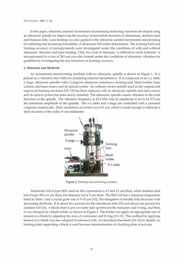
Micromachines 2017, 8, 142
In this paper, ultrasonic assisted incremental microforming technology has been developed usingan ultrasonic spindle for improving the accuracy of microshell structures of aluminium, stainless steel,and titanium foils. Laser heating was also applied to the ultrasonic assisted incremental microformingfor softening and increasing formability of aluminum foil under deformation. The forming limit andforming accuracy of micropyramids were investigated under the conditions of with and withoutultrasonic vibration and laser heating. Only for a foil of titanium—a difficult-to-work material—amicropyramid in a size of 283 µm was also formed under the conditions of ultrasonic vibration forqualitatively investigating the size reduction on forming accuracy.
2. Materials and Methods
An incremental microforming machine with an ultrasonic spindle is shown in Figure 1. It isplaced on a vibration-free table for insulating external disturbances. It is composed of an x-y table,z stage, ultrasonic spindle with a Langevin ultrasonic transducer, forming tool, blank holder, base,column, and laser source and its optical system. An ordinary motor spindle used in the original andimproved forming machines [10–13] has been replaced with an ultrasonic spindle and laser sourceand its optical system has been newly installed. The ultrasonic spindle causes vibration in the axialdirection of the spindle. The vibration frequency is 42.5 kHz and its amplitude is set to be 0.5 µm,the minimum amplitude of the spindle. The x-y table and z-stage are controlled with a personalcomputer numerically. Their resolutions of motion are 0.01 µm, which is small enough to fabricate ashell structure of the order of one millimeter.
Figure 1. Desktop microforming machine.
Aluminum foil of type 8021 used for the experiments is 6.5 and 12 µm-thick, while stainless steelfoil of type 304 is 8 µm-thick and titanium foil is 5 µm-thick. The 8021 foil has a chemical compositionlisted in Table 1 and a crystal grain size of 5–10 µm [15]. The elongation of metallic foils decreases withdecreasing thickness. It is about five percent for the aluminum foils [15] and about one percent forstainless foil [16]. A blank sheet is put on matte side up between the tensioner and O-ring, and then,it was clamped in a blank holder as shown in Figure 2. The holder can apply an appropriate size oftension to a blank by adjusting the sizes of a tensioner and O-ring [10–12]. This method for applyingtension to a blank was also adopted in reference [14]. As described elsewhere [10–12] in details, nobacking plate supporting a blank is used because miniaturization of a backing plate is not easy.
31

Micromachines 2017, 8, 142
Table 1. Chemical composition of 8021 aluminum foil [wt %].
Si Fe Cu Mn Mg Zn Others Al
<0.15 >1.2, <1.7 <0.05 <0.05 <0.05 <0.05 <0.05 Remainder
A single point forming tool of ultra-fine grain cemented carbide with a tip radius of R = 100 µmor 10 µm is used in this study (Figure 3). Before starting microforming, z-position of the top surfaceof a blank was determined accurately by detecting the contact between the tool and blank. n-propylalcohol is used as a lubricant for avoiding adhesion and abrasion between the forming tool and blank.High speed rotation of the tool generates the hydrodynamic pressure between the rotating tool andblank being formed. Under this condition, the alcohol may penetrate into the interface between themif the contact stress is low.
dt
Figure 2. Blank holder and tensioner.
(a) (b)
200 µm
Figure 3. Microtool for incremental microforming: (a) R = 100 µm; (b) R = 10 µm.
Incremental microforming process of a triangular pyramid, for example, is shown in Figure 4,where D is the diameter of a circumscribed circle of a base of a pyramid, α is a half apex angle definedas an angle between a lateral edge and a vertical line through an apex, θ is a half apex angle defined asan angle between a triangular lateral face and the vertical line, t is the thickness of a blank, ω is thetool rotational speed, and ∆z is the axial feed per a planar tool path. The side length of a triangulartool path on a plane shrinks step by step. The tool rotational speed ω and table speed vt were set to be5000 min−1 and 200 µm/s, respectively, except that ω = 10,000 min−1 and vt = 150 µm/s for a titaniummicropyramid of D = 283 µm. The axial feed ∆z was 5 and 12 µm for 6.5 and 12 µm-thick aluminumfoils, respectively, 5 µm for 8 µm-thick stainless steel foil, and 2 and 1 µm for titanium pyramids ofD = 1.41 mm and D = 283 µm, respectively. When the forming was conducted under the condition oflaser heating, the forming area of the foil was irradiated from the top of a pyramid (from the below ofa pyramid) using a semiconductor laser of 130 mW; the laser beam was reflected using a prism underthe blank holder.
32
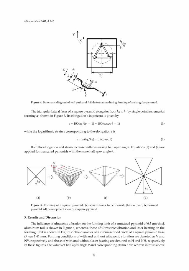
Micromachines 2017, 8, 142
X
Y
Δy
D
Z Δz
h
ω
t α
θ
Figure 4. Schematic diagram of tool path and foil deformation during forming of a triangular pyramid.
The triangular lateral faces of a square pyramid elongates from h0 to h1 by single point incrementalforming as shown in Figure 5. Its elongation e in percent is given by
e = 100(h1/h0 − 1) = 100(cosec θ − 1) (1)
while the logarithmic strain ε corresponding to the elongation e is
ε = ln(h1/h0) = ln(cosec θ) (2)
Both the elongation and strain increase with decreasing half apex angle. Equations (1) and (2) areapplied for truncated pyramids with the same half apex angle θ.
(a) (b) (c) (d)
Figure 5. Forming of a square pyramid: (a) square blank to be formed; (b) tool path; (c) formedpyramid; (d) development view of a square pyramid.
3. Results and Discussion
The influence of ultrasonic vibration on the forming limit of a truncated pyramid of 6.5 µm-thickaluminum foil is shown in Figure 6, whereas, those of ultrasonic vibration and laser heating on theforming limit is shown in Figure 7. The diameter of a circumscribed circle of a square pyramid baseD was 1.41 mm. Forming conditions of with and without ultrasonic vibration are denoted as V andNV, respectively and those of with and without laser heating are denoted as H and NH, respectively.In these figures, the values of half apex angle θ and corresponding strain ε are written in rows above
33
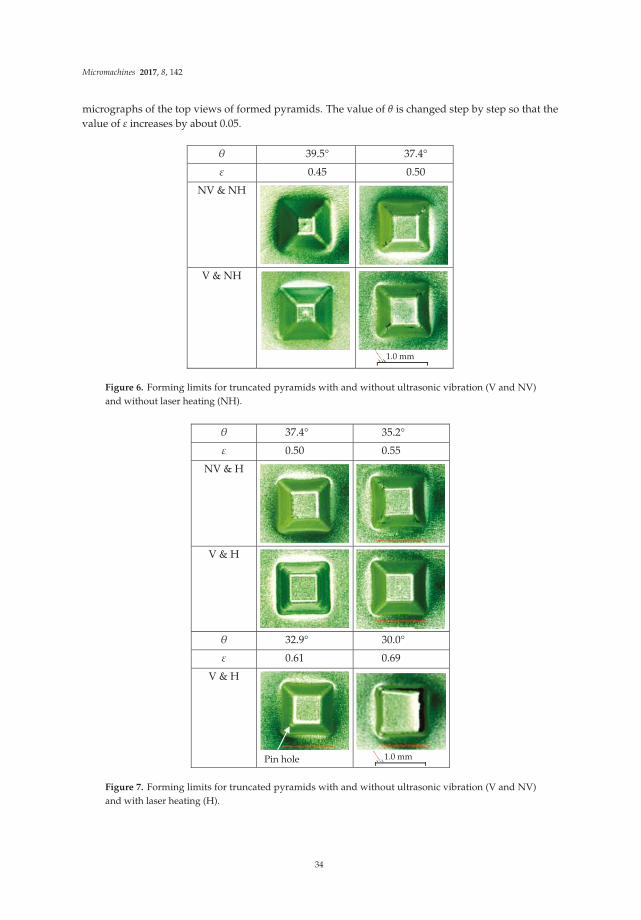
Micromachines 2017, 8, 142
micrographs of the top views of formed pyramids. The value of θ is changed step by step so that thevalue of ε increases by about 0.05.
39.5° 37.4°
0.45 0.50
NV & NH
V & NH
1.0 mm
Figure 6. Forming limits for truncated pyramids with and without ultrasonic vibration (V and NV)and without laser heating (NH).
37.4° 35.2°
0.50 0.55
NV & H
V & H
32.9° 30.0°
0.61 0.69
V & H
1.0 mmPin hole
Figure 7. Forming limits for truncated pyramids with and without ultrasonic vibration (V and NV)and with laser heating (H).
34
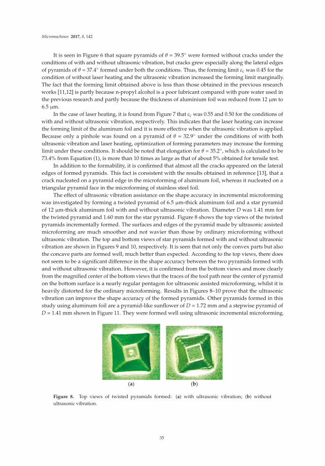
Micromachines 2017, 8, 142
It is seen in Figure 6 that square pyramids of θ = 39.5◦ were formed without cracks under theconditions of with and without ultrasonic vibration, but cracks grew especially along the lateral edgesof pyramids of θ = 37.4◦ formed under both the conditions. Thus, the forming limit εc was 0.45 for thecondition of without laser heating and the ultrasonic vibration increased the forming limit marginally.The fact that the forming limit obtained above is less than those obtained in the previous researchworks [11,12] is partly because n-propyl alcohol is a poor lubricant compared with pure water used inthe previous research and partly because the thickness of aluminium foil was reduced from 12 µm to6.5 µm.
In the case of laser heating, it is found from Figure 7 that εc was 0.55 and 0.50 for the conditions ofwith and without ultrasonic vibration, respectively. This indicates that the laser heating can increasethe forming limit of the aluminum foil and it is more effective when the ultrasonic vibration is applied.Because only a pinhole was found on a pyramid of θ = 32.9◦ under the conditions of with bothultrasonic vibration and laser heating, optimization of forming parameters may increase the forminglimit under these conditions. It should be noted that elongation for θ = 35.2◦, which is calculated to be73.4% from Equation (1), is more than 10 times as large as that of about 5% obtained for tensile test.
In addition to the formability, it is confirmed that almost all the cracks appeared on the lateraledges of formed pyramids. This fact is consistent with the results obtained in reference [13], that acrack nucleated on a pyramid edge in the microforming of aluminum foil, whereas it nucleated on atriangular pyramid face in the microforming of stainless steel foil.
The effect of ultrasonic vibration assistance on the shape accuracy in incremental microformingwas investigated by forming a twisted pyramid of 6.5 µm-thick aluminum foil and a star pyramidof 12 µm-thick aluminum foil with and without ultrasonic vibration. Diameter D was 1.41 mm forthe twisted pyramid and 1.60 mm for the star pyramid. Figure 8 shows the top views of the twistedpyramids incrementally formed. The surfaces and edges of the pyramid made by ultrasonic assistedmicroforming are much smoother and not wavier than those by ordinary microforming withoutultrasonic vibration. The top and bottom views of star pyramids formed with and without ultrasonicvibration are shown in Figures 9 and 10, respectively. It is seen that not only the convex parts but alsothe concave parts are formed well, much better than expected. According to the top views, there doesnot seem to be a significant difference in the shape accuracy between the two pyramids formed withand without ultrasonic vibration. However, it is confirmed from the bottom views and more clearlyfrom the magnified center of the bottom views that the traces of the tool path near the center of pyramidon the bottom surface is a nearly regular pentagon for ultrasonic assisted microforming, whilst it isheavily distorted for the ordinary microforming. Results in Figures 8–10 prove that the ultrasonicvibration can improve the shape accuracy of the formed pyramids. Other pyramids formed in thisstudy using aluminum foil are a pyramid-like sunflower of D = 1.72 mm and a stepwise pyramid ofD = 1.41 mm shown in Figure 11. They were formed well using ultrasonic incremental microforming.
(a) (b)
Figure 8. Top views of twisted pyramids formed: (a) with ultrasonic vibration; (b) withoutultrasonic vibration.
35
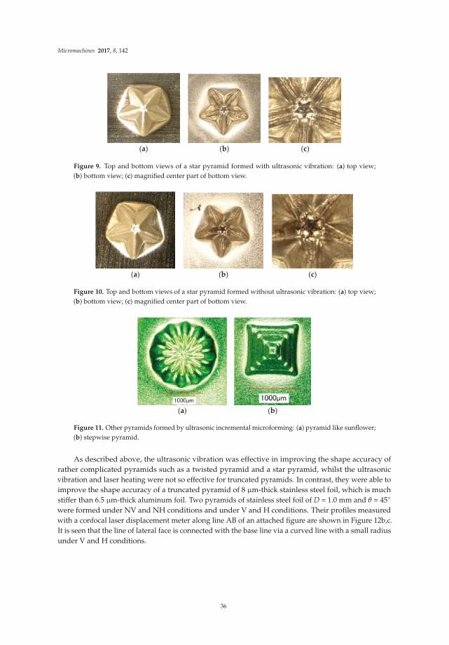
Micromachines 2017, 8, 142
(a) (b) (c)
Figure 9. Top and bottom views of a star pyramid formed with ultrasonic vibration: (a) top view;(b) bottom view; (c) magnified center part of bottom view.
(a) (b) (c)
Figure 10. Top and bottom views of a star pyramid formed without ultrasonic vibration: (a) top view;(b) bottom view; (c) magnified center part of bottom view.
(a) (b)
Figure 11. Other pyramids formed by ultrasonic incremental microforming: (a) pyramid like sunflower;(b) stepwise pyramid.
As described above, the ultrasonic vibration was effective in improving the shape accuracy ofrather complicated pyramids such as a twisted pyramid and a star pyramid, whilst the ultrasonicvibration and laser heating were not so effective for truncated pyramids. In contrast, they were able toimprove the shape accuracy of a truncated pyramid of 8 µm-thick stainless steel foil, which is muchstiffer than 6.5 µm-thick aluminum foil. Two pyramids of stainless steel foil of D = 1.0 mm and θ = 45◦
were formed under NV and NH conditions and under V and H conditions. Their profiles measuredwith a confocal laser displacement meter along line AB of an attached figure are shown in Figure 12b,c.It is seen that the line of lateral face is connected with the base line via a curved line with a small radiusunder V and H conditions.
36
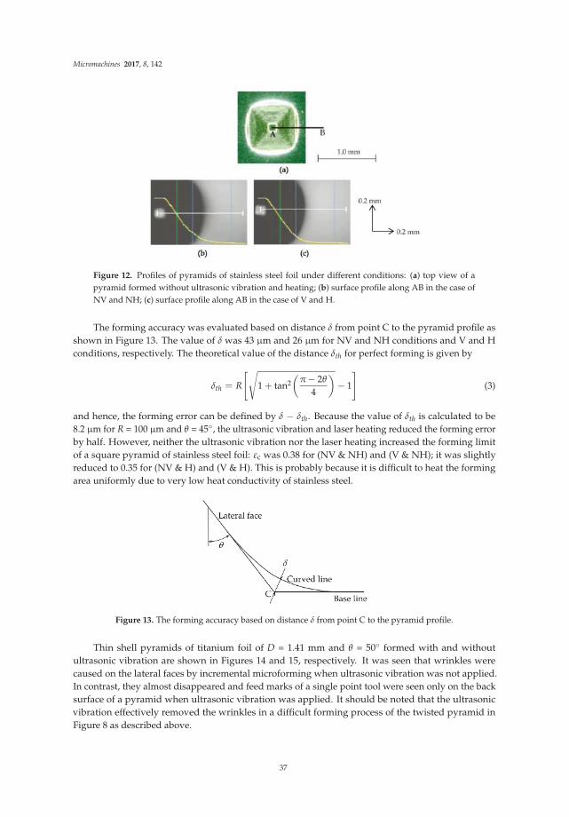
Micromachines 2017, 8, 142
Figure 12. Profiles of pyramids of stainless steel foil under different conditions: (a) top view of apyramid formed without ultrasonic vibration and heating; (b) surface profile along AB in the case ofNV and NH; (c) surface profile along AB in the case of V and H.
The forming accuracy was evaluated based on distance δ from point C to the pyramid profile asshown in Figure 13. The value of δ was 43 µm and 26 µm for NV and NH conditions and V and Hconditions, respectively. The theoretical value of the distance δth for perfect forming is given by
δth = R
[√
1 + tan2(
π− 2θ
4
)
− 1
]
(3)
and hence, the forming error can be defined by δ − δth. Because the value of δth is calculated to be8.2 µm for R = 100 µm and θ = 45◦, the ultrasonic vibration and laser heating reduced the forming errorby half. However, neither the ultrasonic vibration nor the laser heating increased the forming limitof a square pyramid of stainless steel foil: εc was 0.38 for (NV & NH) and (V & NH); it was slightlyreduced to 0.35 for (NV & H) and (V & H). This is probably because it is difficult to heat the formingarea uniformly due to very low heat conductivity of stainless steel.
Figure 13. The forming accuracy based on distance δ from point C to the pyramid profile.
Thin shell pyramids of titanium foil of D = 1.41 mm and θ = 50◦ formed with and withoutultrasonic vibration are shown in Figures 14 and 15, respectively. It was seen that wrinkles werecaused on the lateral faces by incremental microforming when ultrasonic vibration was not applied.In contrast, they almost disappeared and feed marks of a single point tool were seen only on the backsurface of a pyramid when ultrasonic vibration was applied. It should be noted that the ultrasonicvibration effectively removed the wrinkles in a difficult forming process of the twisted pyramid inFigure 8 as described above.
37
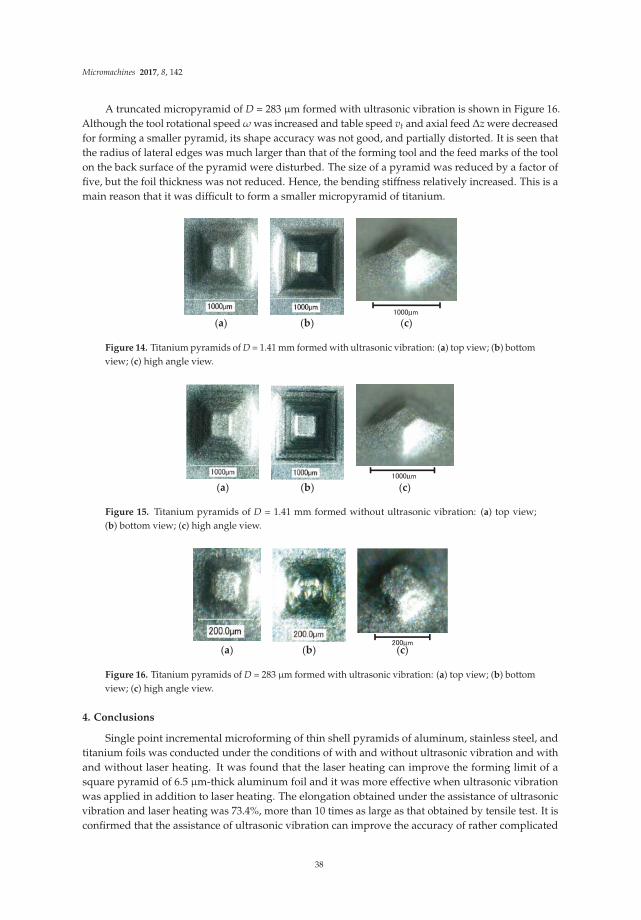
Micromachines 2017, 8, 142
A truncated micropyramid of D = 283 µm formed with ultrasonic vibration is shown in Figure 16.Although the tool rotational speed ω was increased and table speed vt and axial feed ∆z were decreasedfor forming a smaller pyramid, its shape accuracy was not good, and partially distorted. It is seen thatthe radius of lateral edges was much larger than that of the forming tool and the feed marks of the toolon the back surface of the pyramid were disturbed. The size of a pyramid was reduced by a factor offive, but the foil thickness was not reduced. Hence, the bending stiffness relatively increased. This is amain reason that it was difficult to form a smaller micropyramid of titanium.
(a) (b) (c)µ
Figure 14. Titanium pyramids of D = 1.41 mm formed with ultrasonic vibration: (a) top view; (b) bottomview; (c) high angle view.
(a) (b) (c)µ
Figure 15. Titanium pyramids of D = 1.41 mm formed without ultrasonic vibration: (a) top view;(b) bottom view; (c) high angle view.
(a) (b) (c)µ
Figure 16. Titanium pyramids of D = 283 µm formed with ultrasonic vibration: (a) top view; (b) bottomview; (c) high angle view.
4. Conclusions
Single point incremental microforming of thin shell pyramids of aluminum, stainless steel, andtitanium foils was conducted under the conditions of with and without ultrasonic vibration and withand without laser heating. It was found that the laser heating can improve the forming limit of asquare pyramid of 6.5 µm-thick aluminum foil and it was more effective when ultrasonic vibrationwas applied in addition to laser heating. The elongation obtained under the assistance of ultrasonicvibration and laser heating was 73.4%, more than 10 times as large as that obtained by tensile test. It isconfirmed that the assistance of ultrasonic vibration can improve the accuracy of rather complicated
38

Micromachines 2017, 8, 142
shape of pyramids such as a twisted pyramid and a star pyramid. It is also found that ultrasonicvibration improves the forming accuracy of stiff materials or difficult-to-work materials even if theshapes of micropyramids are simple.
Acknowledgments: The authors would like to extend their thanks to cutting tool manufacturers, OSG Corporationand NS Tool Co., Ltd. for the fabrication of microforming tools used in this study. This study is partly basedon projects supported by Amada Foundation (AF-2014023) and JSPS Grant-in-Aids for Challenging ExploratoryResearch (24656097, 2012), Japan. These contributions are gratefully acknowledged.
Author Contributions: T.O. conceived and designed the experiments; M.H. completed the experimentalapparatus, its controlling software, and forming experiments.
Conflicts of Interest: The authors declare no conflict of interest.
References
1. Dornfeld, D.; Min, S.; Takeuchi, Y. Recent advances in mechanical micromachining. CIRP Ann. 2006, 55,
745–768. [CrossRef]
2. Fissi, L.E.L.; Xhurdebise, V.; Francis, L.A. Effects of laser operating parameters on piezoelectric substrates
micromachining with picosecond laser. Micromachines 2015, 6, 19–31. [CrossRef]
3. Zhang, J.; Li, Q.; Zhang, H.; Sui, Y.; Yang, H. Investigation of micro square structure fabrication by applying
textured cutting tool in WEDM. Micromachines 2015, 6, 1427–1434. [CrossRef]
4. Raju, L.; Hiremath, S.S. A State-of-the-art review on micro electro-discharge machining. Procedia Technol.
2016, 25, 1281–1288. [CrossRef]
5. Wang, C.; Guo, B.; Shan, D. Friction related size-effect in microforming—A review. Manuf. Rev. 2014, 1, 23.
[CrossRef]
6. Malinauskas, M.; Rekštyte, S.; Lukoševicius, L.; Butkus, S.; Balciunas, E.; Peciukaityte, M.; Baltriukiene, D.;
Bukelskiene, V.; Butkevicius, A.; Kucevicius, P.; et al. 3D microporous scaffolds manufactured via
combination of fused filament fabrication and direct laser writing ablation. Micromachines 2014, 5, 839–858.
[CrossRef]
7. Jeswiet, J.; Micari, F.; Hirt, G.; Bramley, A.; Duflou, J.; Allwood, J. Asymmetric single point incremental
forming of sheet metal. Ann. CIRP 2005, 54, 88–114. [CrossRef]
8. Matsubara, S. A computer numerically controlled dieless incremental forming of a sheet metal. J. Eng. Manuf.
2001, 215, 959–966. [CrossRef]
9. Iseki, H. An approximate deformation analysis and FEM analysis for the incremental bulging of sheet metal
using a spherical roller. J. Mater. Process. Technol. 2001, 111, 150–154. [CrossRef]
10. Obikawa, T.; Satou, S.; Hakutani, T. Dieless incremental micro forming of miniature shell objects of aluminum
foils. Int. J. Mach. Tools Manuf. 2009, 49, 906–915. [CrossRef]
11. Sekine, T.; Obikawa, T. Single point micro incremental forming of miniature shell structures. J. Adv. Mech.
Des. Syst. Manuf. 2010, 4, 543–557. [CrossRef]
12. Obikawa, T.; Hakutani, T.; Sekine, T.; Numajiri, S.; Matsumura, T.; Yoshino, M. Single-point incremental
micro-forming of thin shell products utilizing high formability. J. Adv. Mech. Des. Syst. Manuf. 2010, 4,
1145–1156. [CrossRef]
13. Obikawa, T.; Sekine, T. Fabrication of miniature shell structures of stainless steel foil and their forming limit
in single point incremental microforming. Int. J. Autom. Techol. 2013, 7, 256–262.
14. Beltran, M.; Malhotra, R.; Nelson, A.J.; Bhattacharya, A.; Reddy, N.V.; Cao, J. Experimental study of failure
modes and scaling effects in micro-incremental forming. J. Micro Nano Manuf. 2013, 1, 031005. [CrossRef]
15. UACJ Foil Corporation. Available online: http://ufo.uacj-group.com/en/products/foil.html (accessed on
28 April 2017).
16. Arai, M.; Ogata, T. Development of small fatigue testing machine for film materials. Trans. Jpn. Soc. Mech. Eng.
2002, 68, 801–806. (In Japanese) [CrossRef]
© 2017 by the authors. Licensee MDPI, Basel, Switzerland. This article is an open access
article distributed under the terms and conditions of the Creative Commons Attribution
(CC BY) license (http://creativecommons.org/licenses/by/4.0/).
39
micromachines
Article
Slurry Injection Schemes on the Extent of SlurryMixing and Availability during ChemicalMechanical Planarization
Matthew Bahr 1,*, Yasa Sampurno 1,2, Ruochen Han 1 and Ara Philipossian 1,2
1 Department of Chemical and Environmental Engineering, University of Arizona, Tucson, AZ 85721, USA;[email protected] (Y.S.); [email protected] (R.H.); [email protected] (A.P.)
2 Araca, Inc., Tucson, AZ 85718, USA* Correspondence: [email protected]; Tel.: +1-(520)-870-4133
Academic Editors: Hans Nørgaard Hansen and Guido ToselloReceived: 30 April 2017; Accepted: 26 May 2017; Published: 29 May 2017
Abstract: In this study, slurry availability and the extent of the slurry mixing (i.e., among fresh slurry,spent slurry, and residual rinse-water) were varied via three different injection schemes. An ultravioletenhanced fluorescence technique was employed to qualitatively indicate slurry availability andits flow on the pad during polishing. This study investigated standard pad center area slurryapplication and a slurry injection system (SIS) that covered only the outer half of the wafer track.Results indicated that the radial position of slurry injection and the alteration of fluid mechanicsby the SIS played important roles in slurry mixing characteristics and availability atop the pad.Removal rates were found to decrease with slurry availability, while a higher degree of slurry mixingdecreased the fraction of fresh slurry and consequently lowered the removal rate. By using a hybridsystem (i.e., a combination of slurry injection via SIS and standard pad center slurry application),the polishing process benefited from higher slurry availability and higher fraction of fresh slurrythan the conventional pad center slurry application and the shorter SIS, individually. This workunderscores the importance of optimum slurry injection geometry and flow for obtaining a morecost-effective and environmentally benign chemical mechanical planarization process.
Keywords: slurry availability; slurry injection system; slurry injection position; chemical mechanicalplanarization; CMP; slurry utilization efficiency
1. Introduction
Chemical mechanical planarization (CMP) is an enabling step in integrated circuit (IC)manufacturing for achieving local and global surface planarity through combined chemical andmechanical means. CMP has been widely used in the semiconductor manufacturing industry since1985 [1]. Previous planarization technologies such as thermal flow and spin-on glass have beenshown to provide adequate local planarity, but CMP is the only technique that additionally providesglobal planarity across the wafer surface [2]. A lack of global surface planarity results in tremendousdifficulties during the following steps of the IC manufacturing process, such as lower photolithographyand etch yields, greater step height variation, greater line-width variation, and the amplification ofprevious layer defects [3]. These variations critically impact and reduce both chip performance andoverall device yield [1]. In addition to planarity, CMP must address issues concerning the surfacequality of the wafer. Many academic and industry studies have shown that by controlling the processparameters and consumable sets, average surface roughness values ranging from 0.5 nm to 2 nm canbe achieved [3–6].
Micromachines 2017, 8, 170 40 www.mdpi.com/journal/micromachines
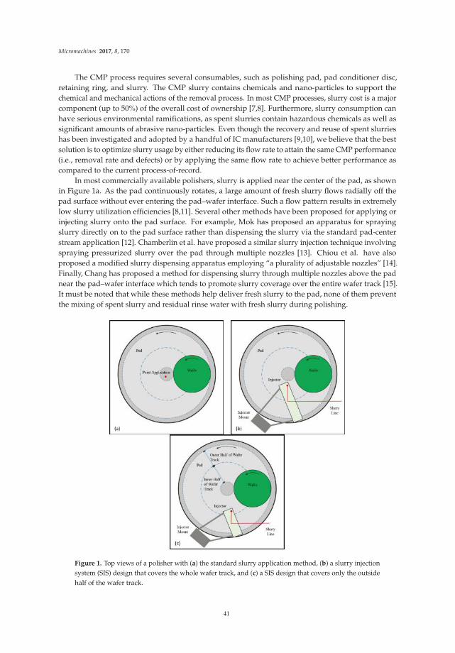
Micromachines 2017, 8, 170
The CMP process requires several consumables, such as polishing pad, pad conditioner disc,retaining ring, and slurry. The CMP slurry contains chemicals and nano-particles to support thechemical and mechanical actions of the removal process. In most CMP processes, slurry cost is a majorcomponent (up to 50%) of the overall cost of ownership [7,8]. Furthermore, slurry consumption canhave serious environmental ramifications, as spent slurries contain hazardous chemicals as well assignificant amounts of abrasive nano-particles. Even though the recovery and reuse of spent slurrieshas been investigated and adopted by a handful of IC manufacturers [9,10], we believe that the bestsolution is to optimize slurry usage by either reducing its flow rate to attain the same CMP performance(i.e., removal rate and defects) or by applying the same flow rate to achieve better performance ascompared to the current process-of-record.
In most commercially available polishers, slurry is applied near the center of the pad, as shownin Figure 1a. As the pad continuously rotates, a large amount of fresh slurry flows radially off thepad surface without ever entering the pad–wafer interface. Such a flow pattern results in extremelylow slurry utilization efficiencies [8,11]. Several other methods have been proposed for applying orinjecting slurry onto the pad surface. For example, Mok has proposed an apparatus for sprayingslurry directly on to the pad surface rather than dispensing the slurry via the standard pad-centerstream application [12]. Chamberlin et al. have proposed a similar slurry injection technique involvingspraying pressurized slurry over the pad through multiple nozzles [13]. Chiou et al. have alsoproposed a modified slurry dispensing apparatus employing “a plurality of adjustable nozzles” [14].Finally, Chang has proposed a method for dispensing slurry through multiple nozzles above the padnear the pad–wafer interface which tends to promote slurry coverage over the entire wafer track [15].It must be noted that while these methods help deliver fresh slurry to the pad, none of them preventthe mixing of spent slurry and residual rinse water with fresh slurry during polishing.
Figure 1. Top views of a polisher with (a) the standard slurry application method, (b) a slurry injectionsystem (SIS) design that covers the whole wafer track, and (c) a SIS design that covers only the outsidehalf of the wafer track.
41
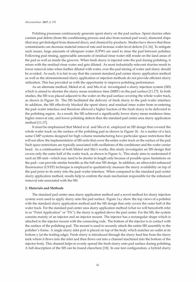
Micromachines 2017, 8, 170
Polishing processes continuously generate spent slurry on the pad surface. Spent slurries oftencontain pad debris (from the conditioning process and also from normal pad wear), diamond chips(that may get dislodged from diamond discs), and chemical by-products. Studies have shown that thesecontaminants can decrease material removal rate and increase wafer-level defects [11,16]. To mitigatesuch issues, large amounts of ultrapure water (UPW) are used to rinse the pad between polishes.Following pad rinsing, appreciable amounts of residual rinse water still reside on the land areas ofthe pad as well as inside the grooves. When fresh slurry is injected onto the pad during polishing, itmixes with the residual rinse water and gets diluted. As most industrially-relevant slurries result inlower removal rates when further diluted with water, over-the-pad mixing of water and slurry shouldbe avoided. As such, it is fair to say that the current standard pad center slurry application methodas well as the aforementioned slurry application or injection methods do not provide efficient slurryutilization. This has provided us with the opportunity to improve polishing performance.
As an alternate method, Meled et al. and Mu et al. investigated a slurry injection system (SIS)which is aimed to shorten the slurry mean residence time (MRT) on the pad surface [11,17]. In bothstudies, the SIS was placed adjacent to the wafer on the pad surface covering the whole wafer track,as shown in Figure 1b. The SIS facilitated the delivery of fresh slurry to the pad–wafer interface.In addition, the SIS effectively blocked the spent slurry and residual rinse water from re-enteringthe pad–wafer interface and therefore allowed a higher fraction of the fresh slurry to be delivered tothe polishing region. As a result, the SIS achieved a significantly lower slurry mean residence time,higher removal rate, and lower polishing defects than the standard pad center area slurry applicationmethod [11,17].
It must be emphasized that Meled et al. and Mu et al. employed an SIS design that covered thewhole wafer track on the surface of the polishing pad as shown in Figure 1b. As a matter of a fact,some CMP systems designed for high volume manufacturing have particular space restrictions thatwill not allow the implementation of SIS units that cover the entire wafer track on the surface of the pad.Such space restrictions are typically associated with oscillations of the conditioner and the wafer carrierhead. As a continuation of both Meled and Mu’s works, this study investigates an SIS design thatcovers only the outer half of the wafer track, as shown in Figure 1c. This study aims to understand ifsuch an SIS unit—which may need to be shorter in length only because of possible space limitations onthe pad—can provide similar benefits as the full-size SIS design. In addition, an ultraviolet enhancedfluorescence (UVEF) technique is employed to qualitatively measure the slurry availability on top ofthe pad prior to its entry into the pad–wafer interface. When compared to the standard pad centerslurry application method, results help to confirm the main mechanism responsible for the enhancedremoval rate associated with the SIS.
2. Materials and Methods
The standard pad center area slurry application method and a novel method for slurry injectionsystem were used to apply slurry onto the pad surface. Figure 1a,c show the top views of a polisherwith the standard slurry application method and the SIS design that only covers the outer half of thewafer track. For the standard pad center area slurry application method (what we will henceforth referto as “Point Application” or “PA”), the slurry is applied above the pad center. For the SIS, the systemconsists mainly of an injector and an injector mount. The injector has a rectangular shape which isattached to the injector mount with the connecting rods. The bottom of the injector is in contact withthe surface of the polishing pad. The mount is used to securely attach the entire SIS assembly to thepolisher’s frame. A single slurry inlet port is placed on top of the body which matches an outlet at itsbottom y (at the trailing edge). Fresh slurry is introduced through the slurry feed line from the slurrytank where it flows into the inlet and then flows out into a channel machined into the bottom of theinjector body. This channel helps to evenly spread the fresh slurry onto pad surface during polishing.A full description of the SIS can be found elsewhere [18]. In one test configuration, a hybrid slurry
42
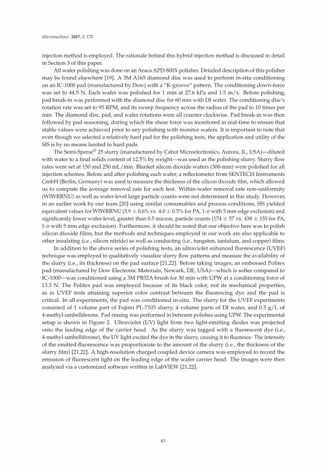
Micromachines 2017, 8, 170
injection method is employed. The rationale behind this hybrid injection method is discussed in detailin Section 3 of this paper.
All wafer polishing was done on an Araca APD-800X polisher. Detailed description of this polishermay be found elsewhere [19]. A 3M A165 diamond disc was used to perform in-situ conditioningon an IC-1000 pad (manufactured by Dow) with a “K-groove” pattern. The conditioning down-forcewas set to 44.5 N. Each wafer was polished for 1 min at 27.6 kPa and 1.5 m/s. Before polishing,pad break-in was performed with the diamond disc for 60 min with DI water. The conditioning disc’srotation rate was set to 95 RPM, and its sweep frequency across the radius of the pad to 10 times permin. The diamond disc, pad, and wafer rotations were all counter clockwise. Pad break-in was thenfollowed by pad seasoning, during which the shear force was monitored in real-time to ensure thatstable values were achieved prior to any polishing with monitor wafers. It is important to note thateven though we selected a relatively hard pad for the polishing tests, the application and utility of theSIS is by no means limited to hard pads.
The Semi-Sperse® 25 slurry (manufactured by Cabot Microelectronics, Aurora, IL, USA)—dilutedwith water to a final solids content of 12.5% by weight—was used as the polishing slurry. Slurry flowrates were set at 150 and 250 mL/min. Blanket silicon dioxide wafers (300-mm) were polished for allinjection schemes. Before and after polishing each wafer, a reflectometer from SENTECH InstrumentsGmbH (Berlin, Germany) was used to measure the thickness of the silicon dioxide film, which allowedus to compute the average removal rate for each test. Within-wafer removal rate non-uniformity(WIWRRNU) as well as wafer-level large particle counts were not determined in this study. However,in an earlier work by our team [20] using similar consumables and process conditions, SIS yieldedequivalent values for WIWRRNU (3.9 ± 0.6% vs. 4.0 ± 0.5% for PA, 1-σ with 5 mm edge exclusion) andsignificantly lower wafer-level, greater than 0.5 micron, particle counts (174 ± 57 vs. 438 ± 155 for PA,1-σ with 5 mm edge exclusion). Furthermore, it should be noted that our objective here was to polishsilicon dioxide films, but the methods and techniques employed in our work are also applicable toother insulating (i.e., silicon nitride) as well as conducting (i.e., tungsten, tantalum, and copper) films.
In addition to the above series of polishing tests, an ultraviolet enhanced fluorescence (UVEF)technique was employed to qualitatively visualize slurry flow patterns and measure the availability ofthe slurry (i.e., its thickness) on the pad surface [21,22]. Before taking images, an embossed Politexpad (manufactured by Dow Electronic Materials, Newark, DE, USA)—which is softer compared toIC-1000—was conditioned using a 3M PB32A brush for 30 min with UPW at a conditioning force of13.3 N. The Politex pad was employed because of its black color, not its mechanical properties,as in UVEF tests attaining superior color contrast between the fluorescing dye and the pad iscritical. In all experiments, the pad was conditioned in-situ. The slurry for the UVEF experimentsconsisted of 1 volume part of Fujimi PL-7103 slurry, 4 volume parts of DI water, and 0.5 g/L of4-methyl-umbelliferone. Pad rinsing was performed in between polishes using UPW. The experimentalsetup is shown in Figure 2. Ultraviolet (UV) light from two light-emitting diodes was projectedonto the leading edge of the carrier head. As the slurry was tagged with a fluorescent dye (i.e.,4-methyl-umbelliferone), the UV light excited the dye in the slurry, causing it to fluoresce. The intensityof the emitted fluorescence was proportionate to the amount of the slurry (i.e., the thickness of theslurry film) [21,22]. A high-resolution charged coupled device camera was employed to record theemission of fluorescent light on the leading edge of the wafer carrier head. The images were thenanalyzed via a customized software written in LabVIEW [21,22].
43

Micromachines 2017, 8, 170
Figure 2. Experimental setup for ultraviolet enhanced fluorescence (UVEF) on an Araca APD-800 Polisher.
3. Results and Discussion
Several published reports indicated that 300-mm CMP processes typically employ slurry flow ratesranging from 250 mL/min to 300 mL/min to achieve optimum material removal rates (RR) [11,23–25].In a separate study, Wang et al. showed that RR increases with the PA slurry flow rate, but it eventuallyreaches an asymptote where further increases in slurry flow rate no longer affect removal rate [26].Philipossian et al. showed that the slurry utilization efficiency (defined as the portion of slurrythat flows through the pad–wafer interface, divided by the total amount of slurry applied) actuallydecreases with an increase in slurry flow rate [8]. Simply increasing slurry flow rate until a certainlevel may help achieve higher RR in several cases, but at a disproportionality higher consumable cost.Therefore, in this study, polishing using the PA method at a slurry flow rate of 250 mL/min (henceforthreferred to as “PA-250”) is considered as our baseline process. Figure 3 summarizes the removal ratesfor all slurry injection methods (to be elaborated in detail later on in this section). As expected, PA atreduced slurry flow rate (i.e., 150 mL/min, henceforth referred to as “PA-150”) yields lower RR thanPA-250. Several published results have reported a similar finding, whereby removal rates are shownto decrease with slurry flow rate [11,26]. One reason for this observation is that at the reduced flowrate, less slurry is available to be transported to the pad–wafer interface [21,27]. Another reason isthe degree of slurry mixing: as discussed in Section 1, during polishing, the fluid residing on thepad surface contains spent slurry, polishing by-products (i.e., pad debris and chemical by-products),and residual rinse water from the pad rinsing procedure performed between polishes which do notcontribute to RR [11,27]. The fresh slurry injected on top of the pad surface gets diluted by mixingwith spent slurry and residual rinse water. The net effect is the reduction of the fraction of fresh slurrydelivered to the polishing region (i.e., between the pad and the wafer) where the removal mechanismoccurs. At reduced slurry flow rate (i.e., the PA-150), the fraction of fresh slurry becomes even lower,thus leading to a lower RR [11,17,27]. As a matter of fact, the traditional PA method does not provide amechanism to promote a higher fraction of fresh slurry. Based on the explanation above, we can inferthat both the degree of slurry mixing and slurry availability affect RR during polishing processes.
44
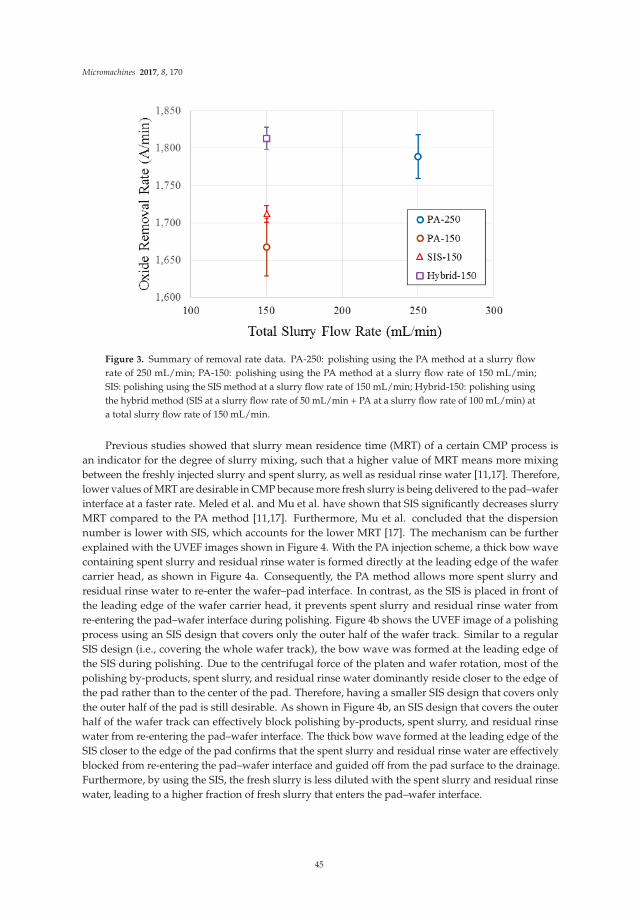
Micromachines 2017, 8, 170
Figure 3. Summary of removal rate data. PA-250: polishing using the PA method at a slurry flowrate of 250 mL/min; PA-150: polishing using the PA method at a slurry flow rate of 150 mL/min;SIS: polishing using the SIS method at a slurry flow rate of 150 mL/min; Hybrid-150: polishing usingthe hybrid method (SIS at a slurry flow rate of 50 mL/min + PA at a slurry flow rate of 100 mL/min) ata total slurry flow rate of 150 mL/min.
Previous studies showed that slurry mean residence time (MRT) of a certain CMP process isan indicator for the degree of slurry mixing, such that a higher value of MRT means more mixingbetween the freshly injected slurry and spent slurry, as well as residual rinse water [11,17]. Therefore,lower values of MRT are desirable in CMP because more fresh slurry is being delivered to the pad–waferinterface at a faster rate. Meled et al. and Mu et al. have shown that SIS significantly decreases slurryMRT compared to the PA method [11,17]. Furthermore, Mu et al. concluded that the dispersionnumber is lower with SIS, which accounts for the lower MRT [17]. The mechanism can be furtherexplained with the UVEF images shown in Figure 4. With the PA injection scheme, a thick bow wavecontaining spent slurry and residual rinse water is formed directly at the leading edge of the wafercarrier head, as shown in Figure 4a. Consequently, the PA method allows more spent slurry andresidual rinse water to re-enter the wafer–pad interface. In contrast, as the SIS is placed in front ofthe leading edge of the wafer carrier head, it prevents spent slurry and residual rinse water fromre-entering the pad–wafer interface during polishing. Figure 4b shows the UVEF image of a polishingprocess using an SIS design that covers only the outer half of the wafer track. Similar to a regularSIS design (i.e., covering the whole wafer track), the bow wave was formed at the leading edge ofthe SIS during polishing. Due to the centrifugal force of the platen and wafer rotation, most of thepolishing by-products, spent slurry, and residual rinse water dominantly reside closer to the edge ofthe pad rather than to the center of the pad. Therefore, having a smaller SIS design that covers onlythe outer half of the pad is still desirable. As shown in Figure 4b, an SIS design that covers the outerhalf of the wafer track can effectively block polishing by-products, spent slurry, and residual rinsewater from re-entering the pad–wafer interface. The thick bow wave formed at the leading edge of theSIS closer to the edge of the pad confirms that the spent slurry and residual rinse water are effectivelyblocked from re-entering the pad–wafer interface and guided off from the pad surface to the drainage.Furthermore, by using the SIS, the fresh slurry is less diluted with the spent slurry and residual rinsewater, leading to a higher fraction of fresh slurry that enters the pad–wafer interface.
45
Micromachines 2017, 8, 170
Figure 4. Bow wave formation on the polishing pad using (a) Point Application (PA) method and(b) the SIS.
SIS increases the slurry availability and reduces the degree of mixing of the fresh slurry withthe spent slurry and residual rinse water. As a result, using the SIS at a reduced slurry flow ratecan achieve similar removal rates compared to PA [11,17,21]. Previous studies on the SIS (that fullycover the whole wafer track) showed that SIS at a slurry flow rate of 150 mL/min achieved the sameremoval rate as PA at a slurry flow rate of 250 mL/min [11,17,21]. Referring back to Figure 3, usingan SIS that only covers the outer half of the wafer track at a flow rate of 150 mL/min (referred to as“SIS-150”) yields an RR that is significantly lower than the PA-250 and only slightly higher than thePA-150. In this configuration, the slurry injection port on the SIS coincides with the center of the wafertrack. Due to rotation and centrifugal forces of both platen and wafer, the injected fresh slurry is thenmainly distributed on the outer half of the wafer track, as illustrated by red color in Figure 5. Therefore,injecting the slurry in the center of the wafer track reduces slurry coverage in the pad–wafer interface,as entering fresh slurry is now reduced to one-half of what was observed when PA and full SIS designswere used. Furthermore, centrifugal forces act more rapidly to pull the slurry off of the pad surface asthe fresh slurry in injected closer to the edge of the pad. Therefore, in this configuration, while SIS isstill effective in blocking the spent slurry and residual rinse water, slurry availability is greatly reducedbecause it only covers the outer half of the wafer track. To increase slurry availability on the inner halfof the wafer track while still taking the benefit of SIS to block the spent slurry and residual rinse waterto re-enter the pad–wafer interface, a hybrid system is proposed as shown in Figure 6.
Figure 5. Coverage of fresh slurry on wafer track (red) using slurry injection system with slurryinjection point coinciding with the center of the wafer track.
46
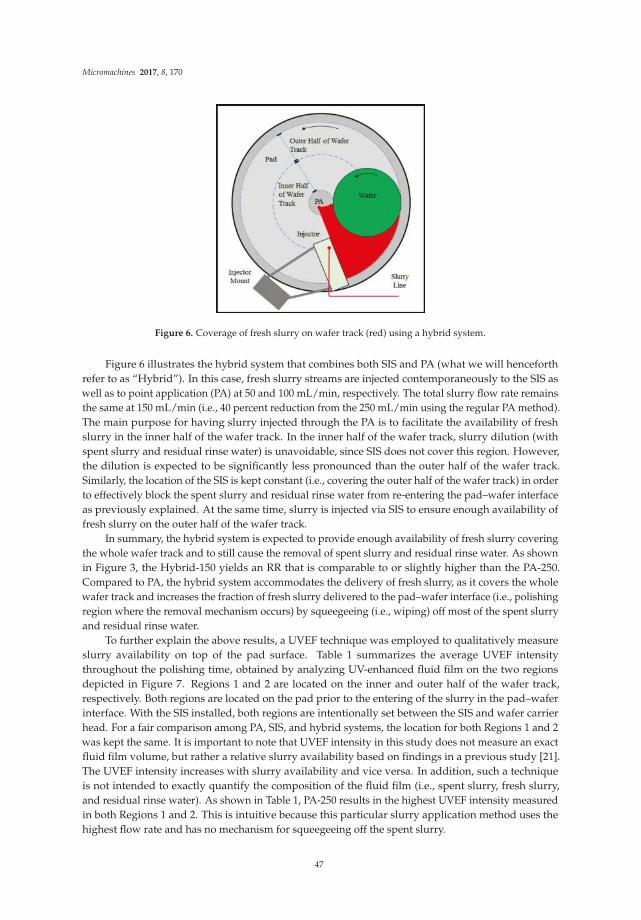
Micromachines 2017, 8, 170
Figure 6. Coverage of fresh slurry on wafer track (red) using a hybrid system.
Figure 6 illustrates the hybrid system that combines both SIS and PA (what we will henceforthrefer to as “Hybrid”). In this case, fresh slurry streams are injected contemporaneously to the SIS aswell as to point application (PA) at 50 and 100 mL/min, respectively. The total slurry flow rate remainsthe same at 150 mL/min (i.e., 40 percent reduction from the 250 mL/min using the regular PA method).The main purpose for having slurry injected through the PA is to facilitate the availability of freshslurry in the inner half of the wafer track. In the inner half of the wafer track, slurry dilution (withspent slurry and residual rinse water) is unavoidable, since SIS does not cover this region. However,the dilution is expected to be significantly less pronounced than the outer half of the wafer track.Similarly, the location of the SIS is kept constant (i.e., covering the outer half of the wafer track) in orderto effectively block the spent slurry and residual rinse water from re-entering the pad–wafer interfaceas previously explained. At the same time, slurry is injected via SIS to ensure enough availability offresh slurry on the outer half of the wafer track.
In summary, the hybrid system is expected to provide enough availability of fresh slurry coveringthe whole wafer track and to still cause the removal of spent slurry and residual rinse water. As shownin Figure 3, the Hybrid-150 yields an RR that is comparable to or slightly higher than the PA-250.Compared to PA, the hybrid system accommodates the delivery of fresh slurry, as it covers the wholewafer track and increases the fraction of fresh slurry delivered to the pad–wafer interface (i.e., polishingregion where the removal mechanism occurs) by squeegeeing (i.e., wiping) off most of the spent slurryand residual rinse water.
To further explain the above results, a UVEF technique was employed to qualitatively measureslurry availability on top of the pad surface. Table 1 summarizes the average UVEF intensitythroughout the polishing time, obtained by analyzing UV-enhanced fluid film on the two regionsdepicted in Figure 7. Regions 1 and 2 are located on the inner and outer half of the wafer track,respectively. Both regions are located on the pad prior to the entering of the slurry in the pad–waferinterface. With the SIS installed, both regions are intentionally set between the SIS and wafer carrierhead. For a fair comparison among PA, SIS, and hybrid systems, the location for both Regions 1 and 2was kept the same. It is important to note that UVEF intensity in this study does not measure an exactfluid film volume, but rather a relative slurry availability based on findings in a previous study [21].The UVEF intensity increases with slurry availability and vice versa. In addition, such a techniqueis not intended to exactly quantify the composition of the fluid film (i.e., spent slurry, fresh slurry,and residual rinse water). As shown in Table 1, PA-250 results in the highest UVEF intensity measuredin both Regions 1 and 2. This is intuitive because this particular slurry application method uses thehighest flow rate and has no mechanism for squeegeeing off the spent slurry.
47
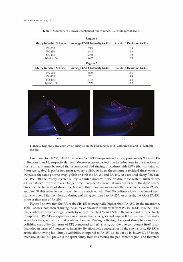
Micromachines 2017, 8, 170
Table 1. Summary of ultraviolet enhanced fluorescence (UVEF) images analysis.
Region 1
Slurry Injection Scheme Average UVEF Intensity (A.U.) Standard Deviation (A.U.)
PA-250 53.5 1.9PA-150 48.8 3.3SIS-150 27.0 1.2
Hybrid-150 44.7 2.5
Region 2
Slurry Injection Scheme Average UVEF Intensity (A.U.) Standard Deviation (A.U.)
PA-250 66.0 3.5PA-150 57.1 3.4SIS-150 41.8 2.4
Hybrid-150 59.9 2.2
(a) (b)
Figure 7. Regions 1 and 2 for UVEF analysis on the polishing pad: (a) with the SIS, and (b) withoutthe SIS.
Compared to PA-250, PA-150 decreases the UVEF image intensity by approximately 9% and 14%in Regions 1 and 2, respectively. Such decreases are expected due to reductions in the injection offresh slurry. It must be noted that a controlled pad rinsing procedure with UPW (that contains nofluorescence dye) is performed prior to every polish. As such, the amount of residual rinse water onthe pad is the same prior to every polish on both the PA-250 and PA-150. At a reduced slurry flow rate(i.e., PA-150), the freshly injected slurry is diluted more with the residual rinse water. Furthermore,a lower slurry flow rate takes a longer time to replace the residual rinse water with the dyed slurry.Since the mechanisms of slurry injection and fluid removal are essentially the same between PA-250and PA-150, this reduction in image intensity associated with PA-150 confirms a lower fraction of freshslurry to overall fluid on the pad during polishing compared to PA-250. As a result, the RR of PA-150is lower than that of PA-250.
Figure 3 shows that the RR of the SIS-150 is marginally higher than PA-150. In the meantime,Table 1 shows that when changing the slurry application mechanism from PA-150 to SIS-150, the UVEFimage intensity decreases significantly by approximately 45% and 27% in Regions 1 and 2, respectively.Compared to PA, SIS incorporates a mechanism that squeegees and wipes off the residual rinse wateras well as the spent slurry that contains the dye. During polishing, the spent slurry has a reducedpolishing capability (in terms of RR) compared to fresh slurry, but the dye component itself is notdegraded in terms of fluorescence intensity. By effectively squeegeeing off the spent slurry, SIS-150 isartificially showing less slurry availability compared to PA-150 as shown by its lower UVEF imageintensity. In fact, SIS prevents the spent slurry from re-entering the pad–wafer region, and therefore
48

Micromachines 2017, 8, 170
the UVEF image intensity associated with SIS in Regions 1 and 2 can be regarded as a much higherfraction of the fresh slurry (i.e., less dilution with spent slurry). Compared to PA-150, the significantdrop of UVEF intensity with SIS-150 in Region 1 is attributed to the absence of slurry injection in theinner half of the wafer track. As a result, only spent slurry contributes to the UVEF intensity with theSIS-150 in Region 1. Region 2 of the SIS-150 has a significantly higher intensity than Region 1 becausethe fresh slurry is injected through the SIS that covers the outer half of the wafer track (i.e., Region 2).The UVEF technique shows that even though SIS-150 can effectively wipe off the spent slurry andresidual rinse water, the fresh slurry is mainly available only to the outer half of the wafer track.
Compared to SIS-150, the Hybrid-150 increases the UVEF intensity of Regions 1 and 2 byapproximately 40% and 30%, respectively. In Region 1, the sharp increase in intensity is attributedto the addition of slurry injection on the inner half of the wafer track. As a result, it increases thefraction of fresh slurry to the overall fluid and hence the slurry availability in the inner half of thewafer track. The increase of intensity in Region 2 also outlines the effect of full wafer track slurrycoverage, as illustrated in Figure 6. The rotation of the platen–wafer ejects the slurry from the innerhalf of the wafer track toward the outer half of the wafer track. Such a mechanism, combined with thefresh slurry injected through the injector, increases slurry availability in Region 2 and thereby causeshigher UVEF intensity. Using the hybrid method, the combined mechanisms of the full slurry coverageand the squeegee effects (of spent slurry and residual rinse water) increase the fraction of fresh slurrywhile maintaining slurry availability on top of the polishing pad during polishing.
4. Conclusions
This work has shown that slurry availability and the extent of slurry mixing (i.e., among freshslurry, spent slurry, and residual rinse water) dramatically influence removal rates. The ultravioletenhanced fluorescence (UVEF) technique showed that injecting fresh slurry solely on the center ofwafer track reduces slurry availability in the pad–wafer interface, as it only covered the outer half ofthe wafer track. Removal rates were found to decrease with slurry availability accordingly. A higherdegree of slurry mixing decreased the fraction of fresh slurry, and consequently lowered the removalrate. In this study, a novel slurry injection system was installed on top of the polishing pad that coveredonly the outer half of the wafer track. UVEF technique confirmed that most of the fluid (i.e., slurry andresidual rinse water) predominantly resided closer to the edge of the pad rather than near the centerof the pad. Therefore, the SIS that covered only the outer half of the wafer track was still effective inblocking the spent slurry and the residual rinse water. This mechanism facilitated the increase in thefraction of fresh slurry on the polishing pad during polishing. In contrast, standard pad center areaslurry application did not have a similar mechanism to block the spent slurry and residual rinse water.
Results further indicated that slurry injection position and the novel SIS played important rolesin slurry mixing characteristics and slurry availability on top of the pad. Injecting fresh slurry at ahigher flow rate and at a location closer to the pad center area generally increased slurry availability.By using a hybrid system (i.e., a combination of slurry injection through the shorter SIS and a standardpad center area slurry application), the polishing process benefited from higher slurry availabilityand higher fraction of fresh slurry than the pad center area slurry application and the shorter SIS,individually. This was verified by the UVEF technique.
Acknowledgments: The authors would like to express their deepest gratitude to the University of Arizona’sdepartment of Chemical and Environmental Engineering for covering the publication costs of this article.
Author Contributions: A.P. and Y.S. conceived the experiments; M.B. and R.H. designed and subsequentlyperformed the experiments; M.B. and Y.S. analyzed the data; A.P. contributed the slurry, wafers, and all polishingand analysis tools; All authors contributed suggestions and participated in meaningful discussions regarding theexperiment and manuscript writing; M.B. wrote the manuscript; Y.S., R.H., and A.P. edited the manuscript.
Conflicts of Interest: The authors declare no conflict of interest.
49

Micromachines 2017, 8, 170
References
1. Landis, H.; Burke, P.; Cote, W.; Hill, W.; Hoffman, C.; Kaanta, C.; Koburger, C.; Lange, W.; Leach, M.; Luce, S.
Integration of Chemical-Mechanical Polishing into CMOS Integrated Circuit Manufacturing. Thin Solid Films
1992, 220, 1–7. [CrossRef]
2. Ali, I.; Roy, S.R.; Shinn, G. Chemical-Mechanical Polishing of Interlayer Dielectric: A Review. Solid State
Technol. 1994, 37, 63.
3. Zantye, P.B.; Kumar, A.; Sikder, A.K. Chemical Mechanical Planarization for Microelectronics Applications.
Mater. Sci. Eng. R Rep. 2004, 45, 89–220. [CrossRef]
4. Zhou, C.; Shan, L.; Hight, J.R.; Danyluk, S.; Ng, S.H.; Paszkowski, A.J. Influence of Collodial Abrasive Size
on Material Removal Rateand Surface Finish in SiO2 Chemical Mechanical Polishing. Tribol. Trans. 2002, 45,
232–238. [CrossRef]
5. Choi, G.; Lee, K.; Kim, N.; Park, J.; Seo, Y.; Lee, W. CMP Characteristics and Optical Property of ITO Thin
Film by Using Silica Slurry with a Variety of Process Parameters. Microelectron. Eng. 2006, 83, 2213–2217.
[CrossRef]
6. Basim, G.B.; Adler, J.J.; Mahajan, U.; Singh, R.K.; Moudgil, B.M. Effect of Particle Size of Chemical Mechanical
Polishing Slurries for Enhanced Polishing with Minimal Defects. J. Electrochem. Soc. 2000, 147, 3523–3528.
[CrossRef]
7. Holland, K.; Hurst, A.; Pinder, H. Improving Cost of Ownership and Performance of CMP Process and
Consumables. Micro 2002, 20, 26–30.
8. Philipossian, A.; Mitchell, E. Slurry Utilization Efficiency Studies in Chemical Mechanical Planarization.
Jpn. J. Appl. Phys. 2003, 42, 7259–7264. [CrossRef]
9. Kettler, D.S. Reclaim, Recycle and Reuse of Oxide Slurry for the CMP Process; SEMICON: Taipei, Taiwan, 2013.
10. Amoroso, N.; Tolla, B.; Boldridge, D. CMP Slurry Recycling System and Methods. U.S. Patent Application
20,120,042,575, 23 February 2012.
11. Meled, A.; Zhuang, Y.; Sampurno, Y.A.; Theng, S.; Jiao, Y.; Borucki, L.; Philipossian, A. Analysis of
A Novel Slurry Injection System in Chemical Mechanical Planarization. Jpn. J. Appl. Phys. 2011, 50,
05EC01:1–05EC01:5. [CrossRef]
12. Mok, P. Apparatus for Dispensing Slurry. U.S. Patent 5,964,413, 12 October 1999.
13. Chamberlin, T.; Miller, M.; Walton, G. Slurry Injection Technique for Chemical Mechanical Planarization.
U.S. Patent 5,997,392, 7 December 1999.
14. Chiou, W.; Chen, Y.; Shih, T.; Jang, S. Slurry Dispenser Having Multiple Adjustable Nozzles. U.S. Patent
6,398,627, 4 Jun 2002.
15. Chang, W. Methods for Enhancing Within-Wafer CMP Uniformity. U.S. Patent 6,929,533, 16 August 2005.
16. Kwon, T.; Cho, B.; Venkatesh, R.; Park, J. Correlation of Polishing Pad Property and Pad Debris on Scratch
Formation During CMP. In Proceedings of the International Conference on Planarization/CMP Technology,
Grenoble, France, 15–17 October 2012; pp. 391–396.
17. Mu, Y.; Han, R.; Sampurno, Y.; Zhang, Y.; Borucki, L.; Philipossian, A. Mean Residence Time and Dispersion
Number Associated with Slurry Injection Methods in Chemical Mechanical Planarization. ECS J. Solid State
Sci. Technol. 2016, 5, P155–P159. [CrossRef]
18. Borucki, L.; Sampurno, Y.; Philipossian, A. Method and Device for the Injection of CMP Slurry. U.S. Patent
8,845,395, 30 September 2014.
19. Fujikoshi Machinery Corporation. APD–800 Polisher and Tribometer. Available online: http://www.aracainc.
com/media/pubs/Polisher_and_Tribometer_300mm.pdf (accessed on 4 February 2016).
20. Philipossian, A.; Borucki, L.; Sampurno, Y.; Zhuang, Y. Novel Slurry Injection System for Improved Slurry
Flow and Reduced Defects in CMP. Solid State Phenom. 2014, 219, 143–147. [CrossRef]
21. Liao, X.; Sampurno, Y.; Zhuang, Y.; Philipossian, A. Effect of Slurry Application/Injection Schemes on
Slurry Availability during Chemical Mechanical Planarization (CMP). Electrochem. Solid State Lett. 2012, 15,
H118–H122. [CrossRef]
22. Liao, X.; Sampurno, Y.; Zhuang, Y.; Rice, A.; Sudargho, F.; Philipossian, A.; Wargo, C. Effect of Retaining
Ring Slot Designs and Polishing Conditions on Slurry Flow Dynamics at Bow Wave. Microelectron. Eng.
2012, 98, 70–73. [CrossRef]
50

Micromachines 2017, 8, 170
23. Jiao, Y.; Zhang, Y.; Wei, X.; Sampurno, Y.; Meled, A.; Theng, S.; Cheng, J.; Hooper, D.; Moinpour, M.;
Philipossian, A. Pad Wear Analysis during Interlayer Dielectric Chemical Mechanical Planarization. ECS J.
Solid State Sci. Technol. 2012, 1, N103–N105. [CrossRef]
24. Kangda, Y.; Shengli, W.; Yuling, L.; Chenwei, W.; Xiang, L. Evaluation of Planarization Capability of Copper
Slurry in the CMP Process. J. Semicond. 2013, 34, 036002:1–036022:4. [CrossRef]
25. Jiao, Y.; Sampurno, Y.; Zhang, Y.; Wei, X.; Meled, A.; Philipossian, A. Tribological, Thermal, and Kinetic
Characterization of 300-mm Copper Chemical Mechanical Planarization Process. Jpn. J. Appl. Phys. 2011, 50,
05EC02:1–05EC02:6. [CrossRef]
26. Wang, Y.G.; Zhang, L.C.; Biddut, A. Chemical Effect on the Material Removal Rate in the CMP of Silicon
Wafers. Wear 2011, 270, 312–316. [CrossRef]
27. Sampurno, Y.; Borucki, L.; Philipossian, A. Effect of Slurry Injection Position on Slurry Mixing, Friction,
Removal Rate, and Temperature in Copper CMP. J. Electrochem. Soc. 2005, 152, G841–G845. [CrossRef]
© 2017 by the authors. Licensee MDPI, Basel, Switzerland. This article is an open access
article distributed under the terms and conditions of the Creative Commons Attribution
(CC BY) license (http://creativecommons.org/licenses/by/4.0/).
51
micromachines
Article
Fabrication of Functional Plastic Parts UsingNanostructured Steel Mold Inserts
Nicolas Blondiaux 1,*, Raphaël Pugin 1, Gaëlle Andreatta 1, Lionel Tenchine 2,
Stéphane Dessors 2, Pierre-François Chauvy 3, Matthieu Diserens 3 and Philippe Vuillermoz 4
1 Centre Suisse d’électronique et de Microtechnique CSEM, 1 rue Jaquet-Droz, CH-2002 Neuchatel,Switzerland; [email protected] (R.P.); [email protected] (G.A.)
2 Centre Technique Industriel de la Plasturgie et des Composites-IPC, 2 rue Pierre et Marie Curie,01100 Bellignat, France; [email protected] (L.T.); [email protected] (S.D.)
3 Micropat SA, 30 Côtes-de-Montbenon, CH-1003 Lausanne, Switzerland; [email protected] (P.-F.C.);[email protected] (M.D.)
4 Vuillermoz SAS, 5 rue du Tomachon, 39200 Saint-Claude, France; [email protected]* Correspondence: [email protected]; Tel.: +41-32-720-55-38
Academic Editors: Hans Nørgaard Hansen, Guido Tosello, Andreas Richter and Nam-Trung NguyenReceived: 6 April 2017; Accepted: 25 May 2017; Published: 6 June 2017
Abstract: We report on the fabrication of sub-micro and nanostructured steel mold inserts forthe replication of nanostructured immunoassay biochips. Planar and microstructured stainlesssteel inserts were textured at the sub-micron and nanoscale by combining nanosphere lithographyand electrochemical etching. This allowed the fabrication of structures with lateral dimensions ofhundreds of nanometers and aspect ratios of up to 1:2. Nanostructured plastic parts were producedby means of hot embossing and injection molding. Surface nanostructuring was used to controlwettability and increase the sensitivity of an immunoassay.
Keywords: nanostructures; hot embossing; injection molding; polymer; 3D; steel; mold; wettability;immunoassay
1. Introduction
There is a growing trend for the fabrication of smart products with novel functionalities orenhanced performances. One route to achieve this goal is an accurate control of surface properties.Surface chemistry, topography and a combination of both can be engineered and optimized forspecific applications. Surfaces with controlled topographies have, for example, been manufacturedto reduce the adhesion of bacteria or living adherent cells [1,2] and to control friction and adhesionbetween surfaces [3]. The effect of surface roughness on wettability is a widely studied field [4].Mimicking the well-known lotus effect has been the focus of many studies for the fabrication ofsuperhydrophobic surfaces with controlled wetting states, for example, Cassie–Baxter vs. the Wenzelstate [5,6]. As reported by Martines et al., the processing of silicon-based materials using advancedlithographic techniques allows the design and fabrication of surfaces with a high degree of control oversurface chemistry and topography [7]. Plastic parts with controlled wettability have also been producedusing replication techniques such as hot embossing and injection molding, however, the productionof highly liquid-repellent plastic surfaces without any surface treatment remains challenging [8].Another field of application relevant to this study is the use of surface micro- and nanostructuring toenhance the performance of sensors for biomedical and point-of-care diagnostics [9]. Highly sensitiveplasmonic [10,11] and surface enhanced Raman spectroscopy (SERS) sensors have been produced byoptimizing surface structures on metallic layers, with enhancement factors of up to 108 compared to onflat surfaces [12]. Another way to improve the sensitivity of sensors is to increase the specific area of the
Micromachines 2017, 8, 179 52 www.mdpi.com/journal/micromachines
Micromachines 2017, 8, 179
sensing element. This has been shown by Ingham et al., who used anodized alumina to create highlyporous sensors with surface areas two to three orders of magnitude greater than flat surfaces [13].Kim et al. also reported a significant increase in the fluorescence intensity (four times greater comparedto a flat surface) after fabricating quartz nanopillars on the surface of a DNA biosensor [14]. Such aneffect was also demonstrated by Kuwabara et al. [15] on polystyrene immunoassay chips using ananoimprinting process. By using a specific elongation process during nanoimprinting, high aspectratio pillars were produced, giving rise to a 34-fold increase in the fluorescence intensity.
The examples mentioned above confirm the potential benefits of surface micro- andnanostructuring and show that various techniques have been used to produce specific structuresin different materials. One of the objectives of this study was to produce nanostructured, functionalparts using replication techniques such as hot embossing and injection molding. One of the key points,therefore, is the fabrication of nanostructured mold inserts. Although the process chain developedfor the production of CDs and DVDs is well established for the fabrication of nanostructured nickelstampers, there is an increasing interest to produce steel mold inserts. The main motivations are theease of integration in standard injection molds, the wide range of materials with better durabilityand the possibility of combining different techniques to process inserts at different length scaleswithout being limited by the thickness of the electroformed stamper. Conventional techniques such asmicromilling, laser ablation and wire electrical discharge machining (EDM) are well established for themicrostructuring of steels [16,17]. These are cost effective and allow the fabrication of high aspect ratiostructures on freeform shapes, but have a resolution limited to few micrometers. Alternatively,advanced lithography techniques have been developed for the microelectronic industry duringthe last few decades. UV, X-ray, interference and e-beam lithography, when combined with othermicrofabrication processes such as thin film deposition and etching, have paved the way for thefabrication of nanostructured surfaces and devices [18,19]. Emerging bottom-up approaches such asblock copolymer and nanosphere lithography have also appeared with the common goal of fabricatingsmaller structures [20,21]. These techniques are state of the art with regard to resolution, but they arelimited to planar substrates and have mainly been applied to silicon-based materials. When combinedwith electroforming, structured nickel stamps form the basis of the production of CDs and DVDs.Several studies report the use of photolithography to fabricate structured steel surfaces. Compared tostandard microstructuring techniques such as milling or EDM, this involves the fabrication of an etchmask, followed by the etching of the substrate. In photochemical etching, standard photolithographyis combined with chemical etching for the fabrication of a micropart or for surface microstructuring asshown by Hao et al., Masuzawa et al. and Mason et al. [22–24]. However, one drawback of chemicaletching is the significant increase in the surface roughness of the etched surface, which results fromthe chemical etching solution used and the microstructure of the steel. This can be overcome byusing an electrochemical etching technique, which leads to a mirror-polished surface in the etchedareas. Landolt et al. made comprehensive reviews on the effect of the main parameters affectingelectrochemical etching for titanium and stainless steel surfaces [25–27]. Usually limited to an isotropicprofile, electrochemical etching has also been used in a sequential Bosch-like process to create higheraspect ratio structures, as reported by Shimizu et al. [28]. Finally, physical etching techniques have alsobeen used for the fabrication of nanostructured steel surfaces. An alternative to wet etching techniqueshas been proposed by Al-Azawil et al., who combined photolithography and ion beam etching forthe surface structuring of injection mold inserts. The very low selectivity of ion beam etching allowedhomogeneous etching of the steel surface despite the heterogeneity of the material (Cr, Ni content,presence of MnS inclusions, steel microstructure) [29]. This technique was also used by Kurhihara et al.with a layer of nanoparticles as an etch mask [30]. Although the nanoparticle layers used as etch masksare not as well defined as etch masks made by photolithography, this approach allowed the processingof curved injection molding dies for the fabrication of optical lenses with improved antireflectivity.
When specifically considering the surface structuring of injection mold inserts, the process chaindeveloped for CDs and DVDs remains state of the art for the injection molding of nanostructured
53
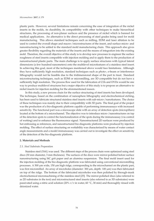
Micromachines 2017, 8, 179
plastic parts. However, several limitations remain concerning the ease of integration of the nickelinserts in the molds, its durability, its compatibility with other techniques to make hierarchicalstructures, the processing of non-planar surfaces and the presence of nickel which is banned formedical applications. An alternative is the direct processing of steel grades being used for moldmanufacturing. This allows standard techniques such as milling, EDM and laser ablation to beused to control the overall shape and macro-/microstructures of the insert, and surface micro- andnanostructuring to be added to the standard mold manufacturing chain. This approach also givesgreater flexibility regarding the materials of the inserts and the means of integration into the existingmold. Therefore, the overall objective of this study is to develop new processes to engineer the surfaceroughness of steel inserts compatible with injection molding and to apply them to the production ofnanostructured plastic parts. The main challenge is to apply surface structures with typical lateraldimensions (a few hundred nanometers) onto the multilevel microfeatures of a stainless steel insert.In achieving this goal, most of the techniques mentioned above would face limitations. Althoughthey have sufficiently high resolution, standard techniques such as photo-, e-beam or interferencelithography would not be feasible due to the tridimensional shape of the part to treat. Standardmicrostructuring techniques, such as EDM or micromilling, are 3D compatible but do not have asufficiently high resolution. The process flow used for the fabrication of CDs and DVDs would be oneway to produce multilevel structures but a major objective of this study is to propose an alternative tonickel inserts for injection molding for the aforementioned reason.
In this study, a new process chain for the surface structuring of steel inserts has been developed.The technique, based on the combination of nanosphere lithography and electrochemical etching,has been used to fabricate structured stainless steel inserts with sub-micro-/nanofeatures. The choiceof these techniques was mainly due to their compatibility with 3D parts. The final goal of the projectwas the production of a bio-diagnostic platform capable of performing immunoassays with increasedsensitivity. The functional part was a microscope slide with an array of detection spots (micropillars)located at the bottom of a microchannel. The objective was to introduce micro-/nanostructures on topof the detection spots to control the functionalization of the spots during the immunoassay (via controlof wetting) and to enhance the fluorescence signal. Nanostructured 2D surfaces were produced byhot embossing as references, and nanostructured bio-diagnostic platforms were produced by injectionmolding. The effect of surface structuring on wettability was characterized by means of water contactangle measurements and a model immunoassay was carried out to investigate the effect on sensitivityof the detection of the bio-diagnostic platform.
2. Materials and Methods
2.1. Steel Substrate Preparation
Stainless steel (316L) was used. The different steps of the process chain were optimized using steeldiscs (30 mm diameter, 3 mm thickness). The surfaces of the discs were mirror-polished before surfacenanostructuring using SiC grit paper and an alumina suspension. The final mold insert used forthe injection molding of the bio-diagnostic platform was fabricated using conventional micromillingprocesses. A 500 µm wide, 150 µm high ridge, corresponding to the microchannel on the plastic part,was first micromilled. An array of microholes (diameter: 300 µm, depth: 100 µm) was then fabricatedon top of the ridge. The bottom of the fabricated microholes was then polished by through-maskelectrochemical micromachining of the stainless steel [25]. The mirror-polished discs (also referred toas 2D substrates in the text) and microstructured steel inserts (also referred to as 3D substrates) werepassivated using a nitric acid solution (20% v/v in water, 60 ◦C, 30 min) and thoroughly rinsed withdeionized water.
54
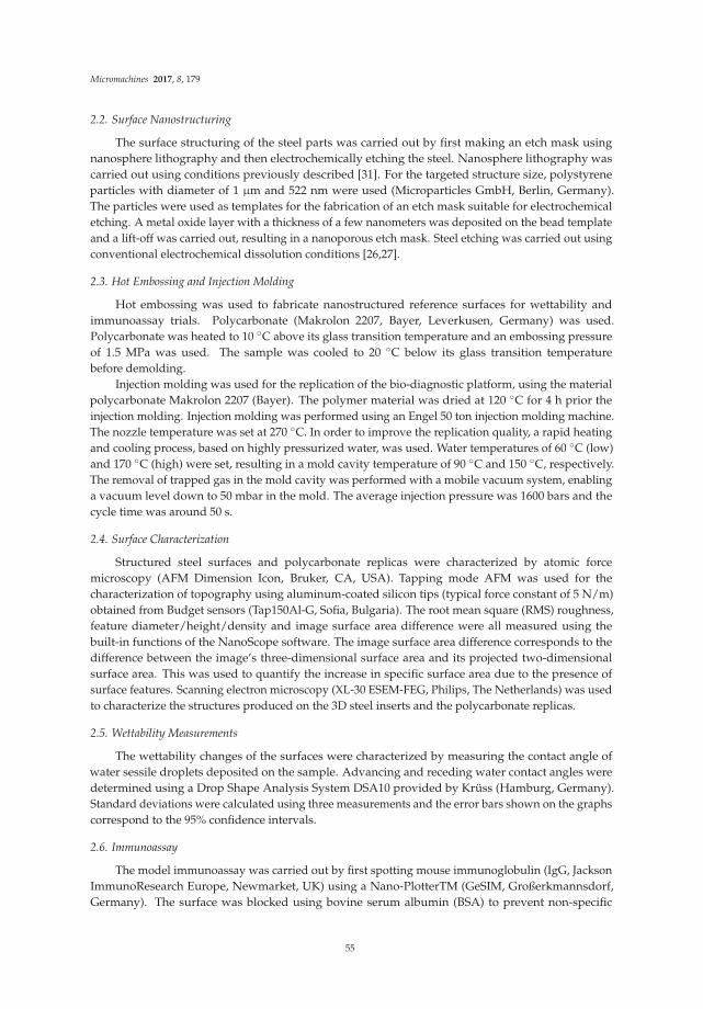
Micromachines 2017, 8, 179
2.2. Surface Nanostructuring
The surface structuring of the steel parts was carried out by first making an etch mask usingnanosphere lithography and then electrochemically etching the steel. Nanosphere lithography wascarried out using conditions previously described [31]. For the targeted structure size, polystyreneparticles with diameter of 1 µm and 522 nm were used (Microparticles GmbH, Berlin, Germany).The particles were used as templates for the fabrication of an etch mask suitable for electrochemicaletching. A metal oxide layer with a thickness of a few nanometers was deposited on the bead templateand a lift-off was carried out, resulting in a nanoporous etch mask. Steel etching was carried out usingconventional electrochemical dissolution conditions [26,27].
2.3. Hot Embossing and Injection Molding
Hot embossing was used to fabricate nanostructured reference surfaces for wettability andimmunoassay trials. Polycarbonate (Makrolon 2207, Bayer, Leverkusen, Germany) was used.Polycarbonate was heated to 10 ◦C above its glass transition temperature and an embossing pressureof 1.5 MPa was used. The sample was cooled to 20 ◦C below its glass transition temperaturebefore demolding.
Injection molding was used for the replication of the bio-diagnostic platform, using the materialpolycarbonate Makrolon 2207 (Bayer). The polymer material was dried at 120 ◦C for 4 h prior theinjection molding. Injection molding was performed using an Engel 50 ton injection molding machine.The nozzle temperature was set at 270 ◦C. In order to improve the replication quality, a rapid heatingand cooling process, based on highly pressurized water, was used. Water temperatures of 60 ◦C (low)and 170 ◦C (high) were set, resulting in a mold cavity temperature of 90 ◦C and 150 ◦C, respectively.The removal of trapped gas in the mold cavity was performed with a mobile vacuum system, enablinga vacuum level down to 50 mbar in the mold. The average injection pressure was 1600 bars and thecycle time was around 50 s.
2.4. Surface Characterization
Structured steel surfaces and polycarbonate replicas were characterized by atomic forcemicroscopy (AFM Dimension Icon, Bruker, CA, USA). Tapping mode AFM was used for thecharacterization of topography using aluminum-coated silicon tips (typical force constant of 5 N/m)obtained from Budget sensors (Tap150Al-G, Sofia, Bulgaria). The root mean square (RMS) roughness,feature diameter/height/density and image surface area difference were all measured using thebuilt-in functions of the NanoScope software. The image surface area difference corresponds to thedifference between the image’s three-dimensional surface area and its projected two-dimensionalsurface area. This was used to quantify the increase in specific surface area due to the presence ofsurface features. Scanning electron microscopy (XL-30 ESEM-FEG, Philips, The Netherlands) was usedto characterize the structures produced on the 3D steel inserts and the polycarbonate replicas.
2.5. Wettability Measurements
The wettability changes of the surfaces were characterized by measuring the contact angle ofwater sessile droplets deposited on the sample. Advancing and receding water contact angles weredetermined using a Drop Shape Analysis System DSA10 provided by Krüss (Hamburg, Germany).Standard deviations were calculated using three measurements and the error bars shown on the graphscorrespond to the 95% confidence intervals.
2.6. Immunoassay
The model immunoassay was carried out by first spotting mouse immunoglobulin (IgG, JacksonImmunoResearch Europe, Newmarket, UK) using a Nano-PlotterTM (GeSIM, Großerkmannsdorf,Germany). The surface was blocked using bovine serum albumin (BSA) to prevent non-specific
55

Micromachines 2017, 8, 179
adsorption (Jackson ImmunoResearch Europe). The excess BSA was then removed by rinsing withphosphate-buffered saline (PBS) with a surfactant (Tween20) and then PBS only. PBS and PBS-Tweenwere supplied by Sigma Aldrich (Buchs, Switzerland). The complementary antibody (αIgG, JacksonImmunoResearch Europe) conjugated to a fluorescent marker (Cy5) was then added. After a lastrinsing step (PBS/Tween 20 and PBS) to remove any αIgG excess, a confocal microscope (TCS-SP5,Leica, Heerbrug, Switzerland) was used to image the detection spots. The amount of fluorescence wascharacterized by measuring the camera-gain necessary to barely reach saturation.
3. Results and Discussion
3.1. Surface Structuring of Flat Stainless Steel (2D Substrate)
The first part of this study focused on the fabrication of sub-micro-/nanostructures on flat,stainless steel substrates.
As shown in Figure 1, the proposed process flow consists of four main steps: first, the depositionof micro-/nanoparticles on the surface of the steel; second, the deposition of a thin (a few nanometersthick) metal oxide layer; third, a lift-off step to remove the particles and produce a porous metal oxideetch mask. Finally, the structures are transferred into the substrate by etching the stainless steel bymeans of an electrochemical dissolution process. The lateral dimensions are controlled via the particledeposition step (particle diameter, particle density). The vertical dimensions are given by the etchingstep (depth, profile).
Figure 1. Schematic showing the process flow used for steel nanostructuring.
In Figure 2, photographs and SEM images of flat stainless steel (316L) surfaces coated withparticles are presented. The presence of the particles leads to a color change effect due to lightscattering. These color changes depend on the size of the particles and the viewing angle and are welldescribed [31]. For 500 nm particles, a monolayer was obtained with a particle density of 1.49 × 10⁸
part·cm−2 and a fill factor of 33%. For 1 µm particles, a density of 2 × 10⁷ part·cm−2 was obtained witha fill factor of 17%. The particle monolayer was then used for the fabrication of an etch mask before theelectrochemical dissolution of the steel. The pattern was transferred into a thin hard mask prior to theelectrochemical dissolution. Figure 3 presents the result obtained using 500 nm beads as templates.
The samples were then electrochemically etched. In Figure 4, a photograph of the steel surface afteretching and the corresponding AFM image of the topography are presented. As for the particle-coatedsurfaces, the transfer of the structures into the steel gave a color change effect on the surface. AFMconfirmed that hemispherical structures were obtained. For an etch mask made using a template of 500nm beads, the average diameter of the final structures after etching was 460 nm with an average depthof 260 nm. One of the main advantage of electrochemical dissolution is the surface quality obtained inthe etched areas, which leads to an RMS roughness on the order of a few nanometers [26]. A range
56
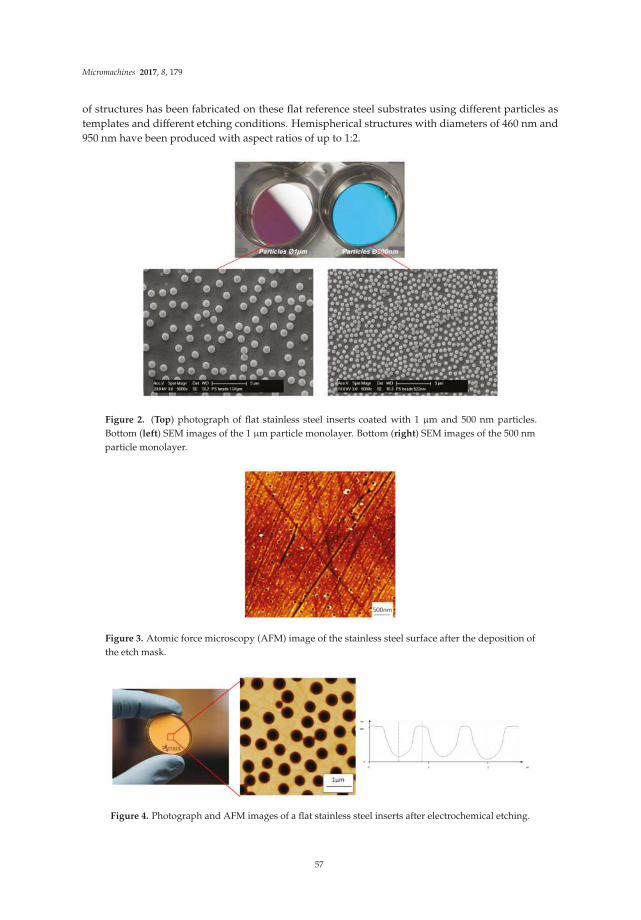
Micromachines 2017, 8, 179
of structures has been fabricated on these flat reference steel substrates using different particles astemplates and different etching conditions. Hemispherical structures with diameters of 460 nm and950 nm have been produced with aspect ratios of up to 1:2.
Figure 2. (Top) photograph of flat stainless steel inserts coated with 1 µm and 500 nm particles.Bottom (left) SEM images of the 1 µm particle monolayer. Bottom (right) SEM images of the 500 nmparticle monolayer.
Figure 3. Atomic force microscopy (AFM) image of the stainless steel surface after the deposition ofthe etch mask.
Figure 4. Photograph and AFM images of a flat stainless steel inserts after electrochemical etching.
57
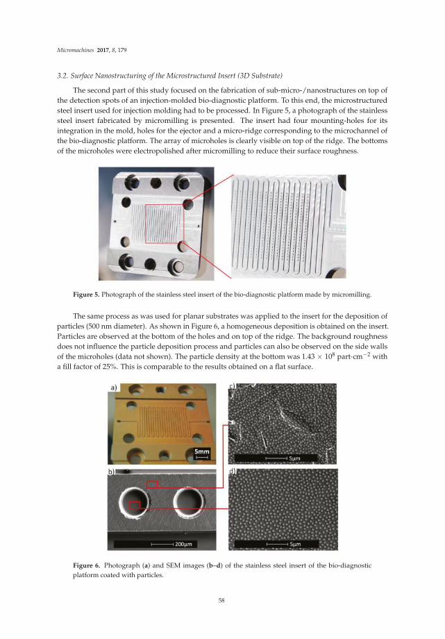
Micromachines 2017, 8, 179
3.2. Surface Nanostructuring of the Microstructured Insert (3D Substrate)
The second part of this study focused on the fabrication of sub-micro-/nanostructures on top ofthe detection spots of an injection-molded bio-diagnostic platform. To this end, the microstructuredsteel insert used for injection molding had to be processed. In Figure 5, a photograph of the stainlesssteel insert fabricated by micromilling is presented. The insert had four mounting-holes for itsintegration in the mold, holes for the ejector and a micro-ridge corresponding to the microchannel ofthe bio-diagnostic platform. The array of microholes is clearly visible on top of the ridge. The bottomsof the microholes were electropolished after micromilling to reduce their surface roughness.
Figure 5. Photograph of the stainless steel insert of the bio-diagnostic platform made by micromilling.
The same process as was used for planar substrates was applied to the insert for the deposition ofparticles (500 nm diameter). As shown in Figure 6, a homogeneous deposition is obtained on the insert.Particles are observed at the bottom of the holes and on top of the ridge. The background roughnessdoes not influence the particle deposition process and particles can also be observed on the side wallsof the microholes (data not shown). The particle density at the bottom was 1.43 × 10⁸ part·cm−2 witha fill factor of 25%. This is comparable to the results obtained on a flat surface.
Figure 6. Photograph (a) and SEM images (b–d) of the stainless steel insert of the bio-diagnosticplatform coated with particles.
58
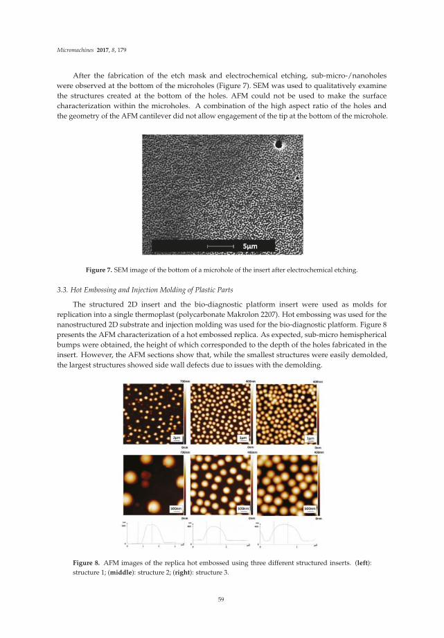
Micromachines 2017, 8, 179
After the fabrication of the etch mask and electrochemical etching, sub-micro-/nanoholeswere observed at the bottom of the microholes (Figure 7). SEM was used to qualitatively examinethe structures created at the bottom of the holes. AFM could not be used to make the surfacecharacterization within the microholes. A combination of the high aspect ratio of the holes andthe geometry of the AFM cantilever did not allow engagement of the tip at the bottom of the microhole.
Figure 7. SEM image of the bottom of a microhole of the insert after electrochemical etching.
3.3. Hot Embossing and Injection Molding of Plastic Parts
The structured 2D insert and the bio-diagnostic platform insert were used as molds forreplication into a single thermoplast (polycarbonate Makrolon 2207). Hot embossing was used for thenanostructured 2D substrate and injection molding was used for the bio-diagnostic platform. Figure 8presents the AFM characterization of a hot embossed replica. As expected, sub-micro hemisphericalbumps were obtained, the height of which corresponded to the depth of the holes fabricated in theinsert. However, the AFM sections show that, while the smallest structures were easily demolded,the largest structures showed side wall defects due to issues with the demolding.
Figure 8. AFM images of the replica hot embossed using three different structured inserts. (left):structure 1; (middle): structure 2; (right): structure 3.
59
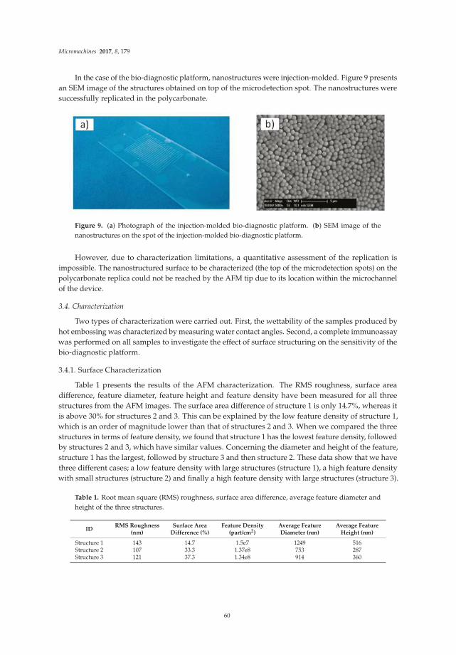
Micromachines 2017, 8, 179
In the case of the bio-diagnostic platform, nanostructures were injection-molded. Figure 9 presentsan SEM image of the structures obtained on top of the microdetection spot. The nanostructures weresuccessfully replicated in the polycarbonate.
Figure 9. (a) Photograph of the injection-molded bio-diagnostic platform. (b) SEM image of thenanostructures on the spot of the injection-molded bio-diagnostic platform.
However, due to characterization limitations, a quantitative assessment of the replication isimpossible. The nanostructured surface to be characterized (the top of the microdetection spots) on thepolycarbonate replica could not be reached by the AFM tip due to its location within the microchannelof the device.
3.4. Characterization
Two types of characterization were carried out. First, the wettability of the samples produced byhot embossing was characterized by measuring water contact angles. Second, a complete immunoassaywas performed on all samples to investigate the effect of surface structuring on the sensitivity of thebio-diagnostic platform.
3.4.1. Surface Characterization
Table 1 presents the results of the AFM characterization. The RMS roughness, surface areadifference, feature diameter, feature height and feature density have been measured for all threestructures from the AFM images. The surface area difference of structure 1 is only 14.7%, whereas itis above 30% for structures 2 and 3. This can be explained by the low feature density of structure 1,which is an order of magnitude lower than that of structures 2 and 3. When we compared the threestructures in terms of feature density, we found that structure 1 has the lowest feature density, followedby structures 2 and 3, which have similar values. Concerning the diameter and height of the feature,structure 1 has the largest, followed by structure 3 and then structure 2. These data show that we havethree different cases; a low feature density with large structures (structure 1), a high feature densitywith small structures (structure 2) and finally a high feature density with large structures (structure 3).
Table 1. Root mean square (RMS) roughness, surface area difference, average feature diameter andheight of the three structures.
IDRMS Roughness
(nm)Surface Area
Difference (%)Feature Density
(part/cm2)Average FeatureDiameter (nm)
Average FeatureHeight (nm)
Structure 1 143 14.7 1.5e7 1249 516Structure 2 107 33.3 1.37e8 753 287Structure 3 121 37.3 1.34e8 914 360
60
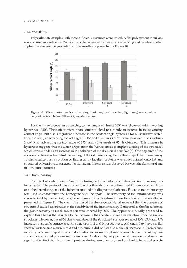
Micromachines 2017, 8, 179
3.4.2. Wettability
Polycarbonate samples with three different structures were tested. A flat polycarbonate surfacewas also used as a reference. Wettability is characterized by measuring advancing and receding contactangles of water used as probe-liquid. The results are presented in Figure 10.
Figure 10. Water contact angles: advancing (dark grey) and receding (light grey) measured onpolycarbonate with four different types of structures.
For the flat reference, an advancing contact angle of almost 100◦ was observed with a wettinghysteresis of 30◦. The surface micro-/nanostructures lead to not only an increase in the advancingcontact angle, but also a significant increase in the contact angle hysteresis for all structures tested.For structure 1, an advancing contact angle of 115◦ and a hysteresis of 57◦ were measured. For structures2 and 3, an advancing contact angle of 135◦ and a hysteresis of 85◦ is obtained. This increase inhysteresis suggests that the water drops are in the Wenzel mode (complete wetting of the structure),which corresponds to an increase in the adhesion of the drop on the surface [5]. One objective of thesurface structuring is to control the wetting of the solution during the spotting step of the immunoassay.To characterize this, a solution of fluorescently labelled proteins was inkjet printed onto flat andstructured polycarbonate surfaces. No significant difference was observed between the flat control andthe structured samples.
3.4.3. Immunoassay
The effect of surface micro-/nanostructuring on the sensitivity of a standard immunoassay wasinvestigated. The protocol was applied to either the micro-/nanostructured hot-embossed surfacesor to the detection spots of the injection-molded bio-diagnostic platforms. Fluorescence microscopywas used to characterize the homogeneity of the spots. The sensitivity of the immunoassay wascharacterized by measuring the gain necessary to reach saturation on the camera. The results arepresented in Figure 11. The quantification of the fluorescence signal revealed that the presence ofstructure 3 caused an increase in the sensitivity of the immunoassay. Compared to the flat reference,the gain necessary to reach saturation was lowered by 30%. The hypothesis initially proposed toexplain this effect is that it is due to the increase in the specific surface area resulting from the surfacestructures. However, the AFM characterization of the structured surfaces revealed 15%, 33% and 37%increases in specific surface area for structures 1, 2 and 3, respectively. Although they have similarspecific surface areas, structure 2 and structure 3 did not lead to a similar increase in fluorescenceintensity. A second hypothesis is that variation in surface roughness has an effect on the adsorptionand conformation of proteins on the surfaces. As shown by Scoppeliti et al., surface roughness cansignificantly affect the adsorption of proteins during immunoassays and can lead to increased protein
61

Micromachines 2017, 8, 179
density on the surface, which may increase the sensitivity of the immunoassay [32]. A third hypothesisis that the interaction of light with the surface structures may influence the fluorescence emissionlevel. Highly sensitive sensors have been produced using optical interference to improve fluorescencesignal [33]. In a previous publication, we showed that particle monolayers deposited on a surface leadto significant optical effects due to the interference between the incident light and the light scattered bythe particles [31]. This size-dependent effect is also expected to have occurred with the hemisphericalstructures of this study. One other hypothesis, therefore, is that the signal enhancement is due to anoptical interference effect caused by the presence of the structures. A more detailed analysis of theoptical properties of the structured surfaces in the immunoassay medium is needed to confirm thishypothesis and the origin of this enhancement.
Figure 11. Confocal images of the fluorescent spots printed on a hot embossed sample (a) andinjection-molded samples (b). (c) Graph presenting the gains necessary to reach saturation on thefluorescent camera.
4. Conclusions
The fabrication of micro-/nanostructured steel surfaces has been achieved by combiningnanosphere lithography and electrochemical etching. Structures with lateral sizes of 400 nm to1 µm with an aspect ratio of 1:2 were produced. The process was applied to planar substrates as well
62
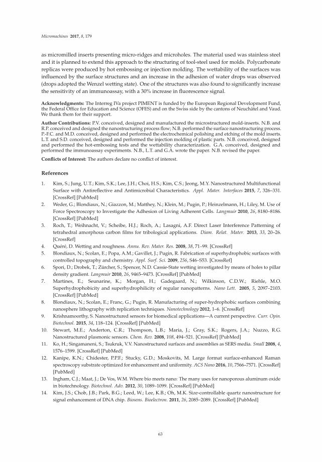
Micromachines 2017, 8, 179
as micromilled inserts presenting micro-ridges and microholes. The material used was stainless steeland it is planned to extend this approach to the structuring of tool-steel used for molds. Polycarbonatereplicas were produced by hot embossing or injection molding. The wettability of the surfaces wasinfluenced by the surface structures and an increase in the adhesion of water drops was observed(drops adopted the Wenzel wetting state). One of the structures was also found to significantly increasethe sensitivity of an immunoassay, with a 30% increase in fluorescence signal.
Acknowledgments: The Interreg IVa project PIMENT is funded by the European Regional Development Fund,the Federal Office for Education and Science (OFES) and on the Swiss side by the cantons of Neuchâtel and Vaud.We thank them for their support.
Author Contributions: P.V. conceived, designed and manufactured the microstructured mold-inserts. N.B. andR.P. conceived and designed the nanostructuring process flow; N.B. performed the surface nanostructuring process.P.-F.C. and M.D. conceived, designed and performed the electrochemical polishing and etching of the mold inserts.L.T. and S.D. conceived, designed and performed the injection molding of plastic parts. N.B. conceived, designedand performed the hot-embossing tests and the wettability characterization. G.A. conceived, designed andperformed the immunoassay experiments. N.B., L.T. and G.A. wrote the paper. N.B. revised the paper.
Conflicts of Interest: The authors declare no conflict of interest.
References
1. Kim, S.; Jung, U.T.; Kim, S.K.; Lee, J.H.; Choi, H.S.; Kim, C.S.; Jeong, M.Y. Nanostructured Multifunctional
Surface with Antireflective and Antimicrobial Characteristics. Appl. Mater. Interfaces 2015, 7, 326–331.
[CrossRef] [PubMed]
2. Weder, G.; Blondiaux, N.; Giazzon, M.; Matthey, N.; Klein, M.; Pugin, P.; Heinzelmann, H.; Liley, M. Use of
Force Spectroscopy to Investigate the Adhesion of Living Adherent Cells. Langmuir 2010, 26, 8180–8186.
[CrossRef] [PubMed]
3. Roch, T.; Weihnacht, V.; Scheibe, H.J.; Roch, A.; Lasagni, A.F. Direct Laser Interference Patterning of
tetrahedral amorphous carbon films for tribological applications. Diam. Relat. Mater. 2013, 33, 20–26.
[CrossRef]
4. Quéré, D. Wetting and roughness. Annu. Rev. Mater. Res. 2008, 38, 71–99. [CrossRef]
5. Blondiaux, N.; Scolan, E.; Popa, A.M.; Gavillet, J.; Pugin, R. Fabrication of superhydrophobic surfaces with
controlled topography and chemistry. Appl. Surf. Sci. 2009, 256, S46–S53. [CrossRef]
6. Spori, D.; Drobek, T.; Zürcher, S.; Spencer, N.D. Cassie-State wetting investigated by means of holes to pillar
density gradient. Langmuir 2010, 26, 9465–9473. [CrossRef] [PubMed]
7. Martines, E.; Seunarine, K.; Morgan, H.; Gadegaard, N.; Wilkinson, C.D.W.; Riehle, M.O.
Superhydrophobicity and superhydrophilicity of regular nanopatterns. Nano Lett. 2005, 5, 2097–2103.
[CrossRef] [PubMed]
8. Blondiaux, N.; Scolan, E.; Franc, G.; Pugin, R. Manufacturing of super-hydrophobic surfaces combining
nanosphere lithography with replication techniques. Nanotechnology 2012, 1–6. [CrossRef]
9. Krishnamoorthy, S. Nanostructured sensors for biomedical applications—A current perspective. Curr. Opin.
Biotechnol. 2015, 34, 118–124. [CrossRef] [PubMed]
10. Stewart, M.E.; Anderton, C.R.; Thompson, L.B.; Maria, J.; Gray, S.K.; Rogers, J.A.; Nuzzo, R.G.
Nanostructured plasmonic sensors. Chem. Rev. 2008, 108, 494–521. [CrossRef] [PubMed]
11. Ko, H.; Singamaneni, S.; Tsukruk, V.V. Nanostructured surfaces and assemblies as SERS media. Small 2008, 4,
1576–1599. [CrossRef] [PubMed]
12. Kanipe, K.N.; Chidester, P.P.F.; Stucky, G.D.; Moskovits, M. Large format surface-enhanced Raman
spectroscopy substrate optimized for enhancement and uniformity. ACS Nano 2016, 10, 7566–7571. [CrossRef]
[PubMed]
13. Ingham, C.J.; Maat, J.; De Vos, W.M. Where bio meets nano: The many uses for nanoporous aluminum oxide
in biotechnology. Biotechnol. Adv. 2012, 30, 1089–1099. [CrossRef] [PubMed]
14. Kim, J.S.; Chob, J.B.; Park, B.G.; Leed, W.; Lee, K.B.; Oh, M.K. Size-controllable quartz nanostructure for
signal enhancement of DNA chip. Biosens. Bioelectron. 2011, 26, 2085–2089. [CrossRef] [PubMed]
63

Micromachines 2017, 8, 179
15. Kuwabara, K.; Ogino, M.; Ando, T.; Miyauchi, A. Enhancement of fluorescence intensity from an
immunoassay chip using high-aspect-ratio nanopillars fabricated by nanoimprinting. Appl. Phys. Lett.
2008, 93, 3. [CrossRef]
16. Masuzawa, T. State of the Art of Micromachining. Ann. CIRP 2000, 49, 473–488. [CrossRef]
17. Bieda, M.; Schmädicke, C.; Roch, T.; Lasagni, A. Ultra-low friction on 100Cr6-steel surfaces after direct laser
interference patterning. Adv. Eng. Mater. 2015, 17, 102–108. [CrossRef]
18. Madou, M. Fundamentals of Microfabrication: The Science of Miniaturization; CRC Press: Boca Raton, FL, USA,
2002.
19. Pease, R.F.; Chou, S.Y. Lithography and other patterning techniques for future electronics. Proc. IEEE 2008,
96, 248–270. [CrossRef]
20. Ruiz, R.; Kang, H.; Detcheverry, F.A.; Dobisz, E.; Kercher, D.S.; Albrecht, T.R.; De Pablo, J.J.; Nealey, P.F.
Density multiplication and improved lithography by directed block copolymer assembly. Science 2008, 321,
936–939. [CrossRef] [PubMed]
21. Klein, M.J.K.; Montagne, F.; Blondiaux, N.; Vazquez-Mena, O.; Heinzelmann, H.; Pugin, R.; Brugger, J.;
Savu, V. SiN membranes with submicrometer hole arrays patterned by wafer-scale nanosphere lithography.
J. Vac. Sci. Technol. B 2011, 2, 021012. [CrossRef]
22. Hao, L.; Meng, Y.; Chen, C. Experimental investigation on effects of surface texturing on lubrication of initial
line contacts. Lubr. Sci. 2014, 26, 363–373. [CrossRef]
23. Mason, J.A.; Adams, D.C.; Johnson, Z.; Smith, S.; Davis, A.W.; Wasserman, D. Selective thermal emission
from patterned steel. Opt. Express 2010, 18, 25192. [CrossRef] [PubMed]
24. Rao, P.N.; Kunzru, D. Fabrication of microchannels on stainless steel by wet chemical etching. J. Micromech.
Microeng. 2007, 17, 99–106.
25. Landolt, D.; Chauvy, P.F.; Zinger, O. Electrochemical micromachining, polishing and surface structuring of
metals: Fundamental aspects and new developments. Electrochim. Acta 2003, 48, 3185–3201. [CrossRef]
26. Zinger, O.; Chauvy, P.F.; Landolt, D. Development of titatnium electrochemical microstructuring towards
implant applications. Eur. Cells Mater. 2001, 1, 24–25.
27. Zinger, O.; Chauvy, P.F.; Landolt, D. Scale-resolved electrochemical surface structuring of titanium for
biological applications. J. Electrochem. Soc. 2003, 150, B495–B503. [CrossRef]
28. Shimizu, M.; Yamada, T.; Sasaki, K.; Takada, A.; Nomura, H.; Iguchi, F.; Yugami, H. Anisotropic multi-step
etching for large-area fabrication of surface microstructures on stainless steel to control thermal radiation.
Sci. Technol. Adv. Mater. 2015, 16, 025001–025006. [CrossRef] [PubMed]
29. Al-Azawi1, A.; Smistrup, K.; Kristensen, A. Nanostructuring steel for injection molding tools. J. Micromech.
Microeng. 2014, 24, 055023–055029. [CrossRef]
30. Kurihara, K.; Saitou, Y.; Souma, N.; Makihara, S.; Kato, H.; Nakano, T. Fabrication of nano-structure
anti-reflective lens using platinum nanoparticles in injection moulding. Mater. Res. Express 2015, 2, 015008.
[CrossRef]
31. Guillaumée, M.; Liley, M.; Pugin, R.; Stanley, R. Scattering of light by a single layer of randomly packed
dielectric microspheres giving color effects in transmission. Opt. Express 2008, 16, 1440–1447. [CrossRef]
[PubMed]
32. Scopelliti, P.E.; Borgonovo, A.; Indrieri, M.; Indrieri, M.; Giorgetti, L.; Bongiorno, G.; Carbone, R.; Podesta, A.;
Milani, P. The Effect of Surface Nanometre-Scale Morphology on Protein Adsorption. PLoS ONE 2010, 5,
11862. [CrossRef] [PubMed]
33. Yasuda, M.; Akimoto, T. Highly Sensitive Fluorescence Detection of Avidin/Streptavidin with an Optical
Interference Mirror Slide. Anal. Sci. 2012, 28, 947–952. [CrossRef] [PubMed]
© 2017 by the authors. Licensee MDPI, Basel, Switzerland. This article is an open access
article distributed under the terms and conditions of the Creative Commons Attribution
(CC BY) license (http://creativecommons.org/licenses/by/4.0/).
64
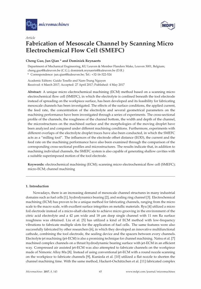
micromachines
Article
Fabrication of Mesoscale Channel by Scanning MicroElectrochemical Flow Cell (SMEFC)
Cheng Guo, Jun Qian * and Dominiek Reynaerts
Department of Mechanical Engineering, KU Leuven & Member Flanders Make, Leuven 3001, Belgium;[email protected] (C.G.); [email protected] (D.R.)* Correspondence: [email protected]; Tel.: +32-16-322-524
Academic Editors: Guido Tosello and Nam-Trung NguyenReceived: 6 March 2017; Accepted: 27 April 2017; Published: 4 May 2017
Abstract: A unique micro electrochemical machining (ECM) method based on a scanning microelectrochemical flow cell (SMEFC), in which the electrolyte is confined beneath the tool electrodeinstead of spreading on the workpiece surface, has been developed and its feasibility for fabricatingmesoscale channels has been investigated. The effects of the surface conditions, the applied current,the feed rate, the concentration of the electrolyte and several geometrical parameters on themachining performance have been investigated through a series of experiments. The cross-sectionalprofile of the channels, the roughness of the channel bottom, the width and depth of the channel,the microstructures on the machined surface and the morphologies of the moving droplet havebeen analyzed and compared under different machining conditions. Furthermore, experiments withdifferent overlaps of the electrolyte droplet traces have also been conducted, in which the SMEFCacts as a “milling tool”. The influences of the electrode offset distance (EOD), the current and thefeed rate on the machining performance have also been examined through the comparison of thecorresponding cross-sectional profiles and microstructures. The results indicate that, in addition tomachining individual channels, the SMEFC system is also capable of generating shallow cavities witha suitable superimposed motion of the tool electrode.
Keywords: electrochemical machining (ECM); scanning micro electrochemical flow cell (SMEFC);micro-ECM; channel machining
1. Introduction
Nowadays, there is an increasing demand of mesoscale channel structures in many industrialdomains such as fuel cells [1], hydrodynamics bearing [2], and sealing ring channel [3]. Electrochemicalmachining (ECM) has proven to be a unique method for fabricating channels, ranging from the microscale to the macro scale, with excellent surface integrities on metallic materials. Ryu [4] utilized a microfoil electrode instead of a micro-shaft electrode to achieve micro grooving in the environment of thecitric acid electrolyte and a 42 µm wide and 18 µm deep single channel with 11 nm Ra surfaceroughness was obtained. Liu et al. [5] has utilized a kind of ECM method with low-frequencyvibrations to fabricate multiple slots for the application of fuel cells. The same features were alsosuccessfully fabricated by other researchers [6], in which they developed an innovative multifunctionalcathode, combining the tool electrode, the sealing device and the spacers between every channels.Electrolyte jet machining (jet-ECM) is also a promising technique for channel machining. Natsu et al. [7]machined complex channels on a thrust hydrodynamic bearing surface with jet-ECM in an efficientway. Compressed air assisted jet-ECM was also attempted to fabricate channels on the workpiecemade of Nimonic Alloy 80a [8]. Instead of using conventional jet-ECM with a round nozzle scanningon the workpiece to fabricate channels [9], Kunieda et al. [10] utilized a flat nozzle to shorten thechannel machining time. With the same method, Hackert-Oschätzchen et al. [11] fabricated complex
Micromachines 2017, 8, 143 65 www.mdpi.com/journal/micromachines
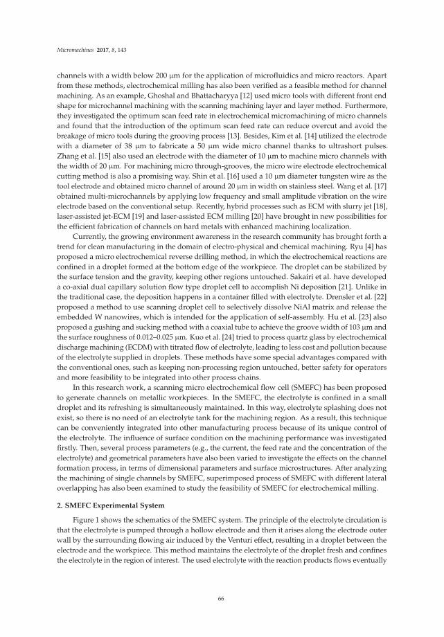
Micromachines 2017, 8, 143
channels with a width below 200 µm for the application of microfluidics and micro reactors. Apartfrom these methods, electrochemical milling has also been verified as a feasible method for channelmachining. As an example, Ghoshal and Bhattacharyya [12] used micro tools with different front endshape for microchannel machining with the scanning machining layer and layer method. Furthermore,they investigated the optimum scan feed rate in electrochemical micromachining of micro channelsand found that the introduction of the optimum scan feed rate can reduce overcut and avoid thebreakage of micro tools during the grooving process [13]. Besides, Kim et al. [14] utilized the electrodewith a diameter of 38 µm to fabricate a 50 µm wide micro channel thanks to ultrashort pulses.Zhang et al. [15] also used an electrode with the diameter of 10 µm to machine micro channels withthe width of 20 µm. For machining micro through-grooves, the micro wire electrode electrochemicalcutting method is also a promising way. Shin et al. [16] used a 10 µm diameter tungsten wire as thetool electrode and obtained micro channel of around 20 µm in width on stainless steel. Wang et al. [17]obtained multi-microchannels by applying low frequency and small amplitude vibration on the wireelectrode based on the conventional setup. Recently, hybrid processes such as ECM with slurry jet [18],laser-assisted jet-ECM [19] and laser-assisted ECM milling [20] have brought in new possibilities forthe efficient fabrication of channels on hard metals with enhanced machining localization.
Currently, the growing environment awareness in the research community has brought forth atrend for clean manufacturing in the domain of electro-physical and chemical machining. Ryu [4] hasproposed a micro electrochemical reverse drilling method, in which the electrochemical reactions areconfined in a droplet formed at the bottom edge of the workpiece. The droplet can be stabilized bythe surface tension and the gravity, keeping other regions untouched. Sakairi et al. have developeda co-axial dual capillary solution flow type droplet cell to accomplish Ni deposition [21]. Unlike inthe traditional case, the deposition happens in a container filled with electrolyte. Drensler et al. [22]proposed a method to use scanning droplet cell to selectively dissolve NiAl matrix and release theembedded W nanowires, which is intended for the application of self-assembly. Hu et al. [23] alsoproposed a gushing and sucking method with a coaxial tube to achieve the groove width of 103 µm andthe surface roughness of 0.012–0.025 µm. Kuo et al. [24] tried to process quartz glass by electrochemicaldischarge machining (ECDM) with titrated flow of electrolyte, leading to less cost and pollution becauseof the electrolyte supplied in droplets. These methods have some special advantages compared withthe conventional ones, such as keeping non-processing region untouched, better safety for operatorsand more feasibility to be integrated into other process chains.
In this research work, a scanning micro electrochemical flow cell (SMEFC) has been proposedto generate channels on metallic workpieces. In the SMEFC, the electrolyte is confined in a smalldroplet and its refreshing is simultaneously maintained. In this way, electrolyte splashing does notexist, so there is no need of an electrolyte tank for the machining region. As a result, this techniquecan be conveniently integrated into other manufacturing process because of its unique control ofthe electrolyte. The influence of surface condition on the machining performance was investigatedfirstly. Then, several process parameters (e.g., the current, the feed rate and the concentration of theelectrolyte) and geometrical parameters have also been varied to investigate the effects on the channelformation process, in terms of dimensional parameters and surface microstructures. After analyzingthe machining of single channels by SMEFC, superimposed process of SMEFC with different lateraloverlapping has also been examined to study the feasibility of SMEFC for electrochemical milling.
2. SMEFC Experimental System
Figure 1 shows the schematics of the SMEFC system. The principle of the electrolyte circulation isthat the electrolyte is pumped through a hollow electrode and then it arises along the electrode outerwall by the surrounding flowing air induced by the Venturi effect, resulting in a droplet between theelectrode and the workpiece. This method maintains the electrolyte of the droplet fresh and confinesthe electrolyte in the region of interest. The used electrolyte with the reaction products flows eventually
66
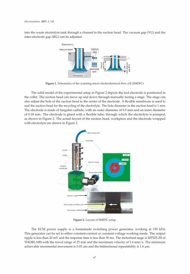
Micromachines 2017, 8, 143
into the waste electrolyte tank through a channel in the suction head. The vacuum gap (VG) and theinter-electrode gap (IEG) can be adjusted.
Figure 1. Schematics of the scanning micro electrochemical flow cell (SMEFC).
The solid model of the experimental setup in Figure 2 depicts the tool electrode is positioned inthe collet. The suction head can move up and down through manually tuning a stage. The stage canalso adjust the hole of the suction head to the center of the electrode. A flexible membrane is used toseal the suction head for the recycling of the electrolyte. The hole diameter in the suction head is 1 mm.The electrode is made of tungsten carbide, with an outer diameter of 0.5 mm and an inner diameterof 0.18 mm. The electrode is glued with a flexible tube, through which the electrolyte is pumped,as shown in Figure 2. The actual layout of the suction head, workpiece and the electrode wrappedwith electrolyte are shown in Figure 2.
Figure 2. Layout of SMEFC setup.
The ECM power supply is a homemade switching power generator, working at 150 kHz.This generator can be set to either constant-current or constant-voltage working mode. The outputripple is less than 20 mV and the response time is less than 50 ms. The motorized stage is MTS25-Z8 ofTHORLABS with the travel range of 25 mm and the maximum velocity of 2.4 mm/s. The minimumachievable incremental movement is 0.05 µm and the bidirectional repeatability is 1.6 µm.
67

Micromachines 2017, 8, 143
The cross-sectional profiles and the roughness of the channels machined by SMEFC have beenmeasured by a Mitutoyo CS3200 profiler (Mitutoyo, Kawasaki, Japan). When measuring the roughness,the workpiece is cleaned firstly in a mixture of ethanol and acetone in an ultrasonic tank. The styluscontacts the bottom surface of the channel and moves along the channel. The nominal radius of thestylus is 2.0 µm. A Zeiss optical microscope (Carl Zeiss AG, Oberkochen, Germany), SteREO DiscoveryV20, was used to evaluate the width of the channels cavities, and Dino-Lite digital microscopeAM4115ZT (AnMo Electronics Corporation, Hsinchu, Taiwan) was installed to help monitor andobserve the moving electrolyte droplet above the workpiece top surface. The maximum lateralresolution of the digital microscope is around 1.4 µm/pixel. The surface microstructures of thechannel bottom surface were examined with a Phenom desktop SEM (Phenom-World B.V., Eindhoven,The Netherlands). The current signals during the electrochemical dissolution were recorded by a dataacquisition unit embedded in the ECM power supply.
3. SMEFC Machining Experiments and Discussion
A series of experiments have been carried out under constant-current mode. The electrolyte isa sodium nitrate (NaNO3) solution with the concentration of 120 g/L and 250 g/L. The workpiecematerial is a kind of stainless steel from UDDEHOLM STAVAX® ESR (Hagfors, Sweden). The electrolyteflow rate is 0.06 mL/s pumped by a metering pump of ProMinent® (ProMinent GmbH, Heidelberg,Germany). The vacuum condition is achieved by a Venturi tube, with an inlet pressure of 4 bar. Thecorresponding vacuum pressure is 45 kPa.
3.1. Experimental Verification
When the droplet moves on the workpiece, the droplet shape will be regulated by its gravity,surface tension and adhesion simultaneously. Therefore, surface conditions or the roughness of theworkpiece may affect the behavior of the moving droplet. To investigate this conjecture, samples withtwo different surface treatments were used. One sample was ground by a surface grinder (Ra = 0.4 µm)and the other one was pre-machined by micro-EDM milling (Ra = 1.2 µm). The surface tension of theelectrolyte is around 75.5 mN/m [25].
Figure 3 shows the profile of the electrolyte droplet moving at different speed on a micro-EDMedsurface. The moving direction of the electrolyte droplet relative to the workpiece has been indicated bythe arrows. The applied current is 230 mA and the feed rates are 0.1 mm/s, 0.2 mm/s, 0.4 mm/s and0.8 mm/s, respectively. It can be noticed that when the scanning speed is 0.1 mm/s, the droplet seemsto be not stable. The electrolyte left on the workpiece can be obviously observed and it crystallizes veryquickly probably due to its exposure to surrounding flowing air. With a slower feed rate, the channelbecomes deeper and the corresponding droplet volume in the channel becomes bigger in the sametime. When the volume reaches a certain level, the surface tension (cohesion) cannot support thevolume in the form of a single droplet. As a result, some of the electrolyte is left on the machinedsurface, as illustrated in Figure 4. Consequently, the electrolyte cannot be fully recovered by theVenturi effect. The electrolyte droplets above the workpiece top surface under the other three feed ratesmaintain a relatively stable shape during the motion. However, when the feed rate goes even higher,the cross-sectional profile perpendicular to the moving direction becomes increasingly asymmetrical.
68

Micromachines 2017, 8, 143
Figure 3. Electrolyte droplet moving on the surface treated by micro-electrical-discharge machining(EDM) milling.
(a) (b)
Figure 4. Explanation of the electrolyte leakage. (a) Surface tension maintains a single droplet;(b) electrolyte left on machined surface once the droplet volume is larger.
Figure 5 depicts the situation when the electrolyte droplet moves on the ground surface with thefeed rates of 0.1 mm/s, 0.2 mm/s and 0.4 mm/s, respectively. Obvious delaying of the electrolytedroplet can be noticed. Compared with the case in Figure 3, the trail above the workpiece top surfacebecomes longer. Obviously, this difference in the droplet morphology is induced by the difference inthe roughness of these two samples.
Figure 5. Electrolyte droplet moving on the ground surface.
69
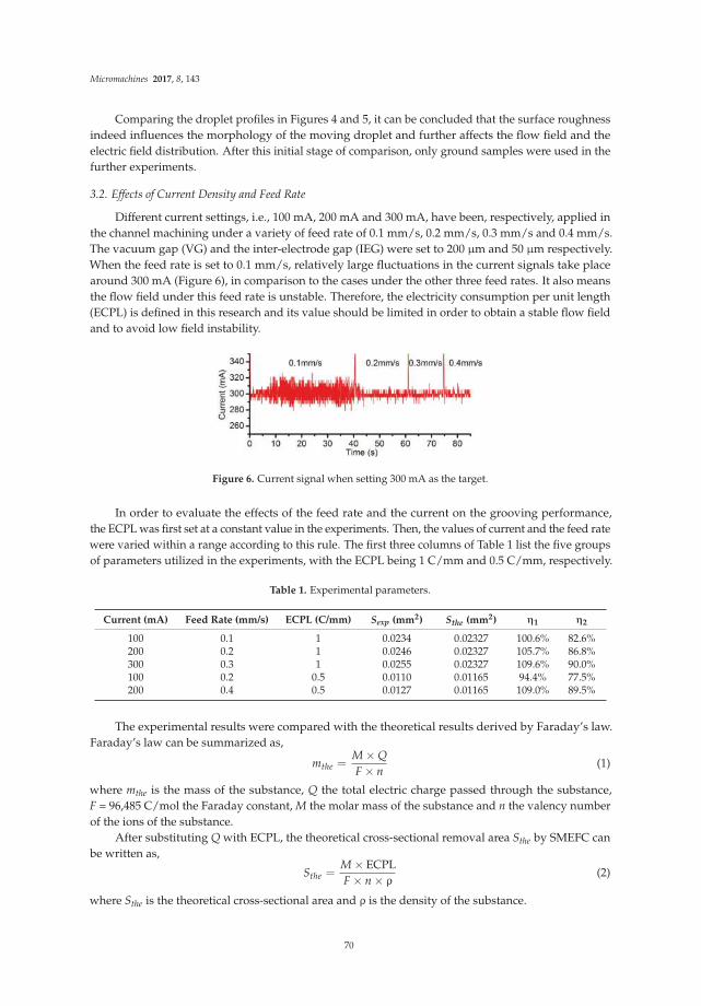
Micromachines 2017, 8, 143
Comparing the droplet profiles in Figures 4 and 5, it can be concluded that the surface roughnessindeed influences the morphology of the moving droplet and further affects the flow field and theelectric field distribution. After this initial stage of comparison, only ground samples were used in thefurther experiments.
3.2. Effects of Current Density and Feed Rate
Different current settings, i.e., 100 mA, 200 mA and 300 mA, have been, respectively, applied inthe channel machining under a variety of feed rate of 0.1 mm/s, 0.2 mm/s, 0.3 mm/s and 0.4 mm/s.The vacuum gap (VG) and the inter-electrode gap (IEG) were set to 200 µm and 50 µm respectively.When the feed rate is set to 0.1 mm/s, relatively large fluctuations in the current signals take placearound 300 mA (Figure 6), in comparison to the cases under the other three feed rates. It also meansthe flow field under this feed rate is unstable. Therefore, the electricity consumption per unit length(ECPL) is defined in this research and its value should be limited in order to obtain a stable flow fieldand to avoid low field instability.
Figure 6. Current signal when setting 300 mA as the target.
In order to evaluate the effects of the feed rate and the current on the grooving performance,the ECPL was first set at a constant value in the experiments. Then, the values of current and the feed ratewere varied within a range according to this rule. The first three columns of Table 1 list the five groupsof parameters utilized in the experiments, with the ECPL being 1 C/mm and 0.5 C/mm, respectively.
Table 1. Experimental parameters.
Current (mA) Feed Rate (mm/s) ECPL (C/mm) Sexp (mm2) Sthe (mm2) η1 η2
100 0.1 1 0.0234 0.02327 100.6% 82.6%200 0.2 1 0.0246 0.02327 105.7% 86.8%300 0.3 1 0.0255 0.02327 109.6% 90.0%100 0.2 0.5 0.0110 0.01165 94.4% 77.5%200 0.4 0.5 0.0127 0.01165 109.0% 89.5%
The experimental results were compared with the theoretical results derived by Faraday’s law.Faraday’s law can be summarized as,
mthe =M × Q
F × n(1)
where mthe is the mass of the substance, Q the total electric charge passed through the substance,F = 96,485 C/mol the Faraday constant, M the molar mass of the substance and n the valency numberof the ions of the substance.
After substituting Q with ECPL, the theoretical cross-sectional removal area Sthe by SMEFC canbe written as,
Sthe =M × ECPLF × n × ρ
(2)
where Sthe is the theoretical cross-sectional area and ρ is the density of the substance.
70

Micromachines 2017, 8, 143
The current efficiency can be described as,
η =mexp
mthe=
Sexp
Sthe(3)
where mexp and Sexp are the experimental removal mass and experimental cross-sectional area,respectively. The valency number n of stainless steel is controversial, because it depends on theproportion of the generated Fe2+ ions and Fe3+ ions. According to the results of [26], whenFe2+:Fe3+ = 1:2, n1 = 3.1410. Using this value, the current efficiency η is calculated to be alwayslarger than 100%. Similar results are also shown in [26], and the uncertain proportion of Fe2+ ionsand Fe3+ ions induce this phenomenon. Therefore, n2 = 2.5786 is also used in the calculations, whichis obtained under the assumption that only Fe2+ ions are generated. η1 and η2 represent the currentefficiency calculated under n1 and n2 respectively. The actual current efficiency should be a valuebetween these two efficiencies. Sthe is calculated under the valency number of n2.
Figure 7 shows the cross-sectional profiles of the channels machined with the parameters inTable 1. It can be observed that when the same ECPL, the maximum depth of these channels is almostthe same in spite of some slight differences (Figure 7). However, as shown in Figure 8, the width of thechannels has clear deviations. At the ECPL of 1 C/mm, the channel width processed by 0.1 mm/s isthe smallest and almost the same width is produced in the cases of 0.2 mm/s and 0.3 mm/s. Similarly,at the ECPL of 0.5 C/mm, the channel width increases with the feed rate. A high concentration(250 g/L) alleviates the trend. There are two possible reasons accountable for this trend. One reasonis that a high current can derive a high current efficiency compared to a low current, which can beconfirmed in the current efficiency in Table 1. The other possible reason is that the contact angle of theelectrolyte droplet is also influenced by the applied voltage. This implies that if a relative voltage isapplied, the electrolyte droplet needs to expand to a bigger area to obtain a smaller contact angle.
Figure 7. Cross-sectional profiles.
Figure 8. Channel width comparison.
Figure 9 indicates that, although the same ECPL can induce relatively uniform depth, the roughnessdeclines along with the increase of the feed rate. Surface microstructures at the channel bottom asshown in Figure 10 also confirm this point when comparing Figure 10a,f,k. Rosenkranz et al. [27]has already pointed out, that during the ECM process, the iron surface is covered by a thin oxidelayer, on top of which a polishing film of supersaturated iron nitrate forms. The thickness of filmvaries with the current density and the electrolyte flow rate, when other parameters do not change.With the increase of the applied current, the surfaces in each column of Figure 10, except the column
71
Micromachines 2017, 8, 143
with the feed rate of 0.1 mm/s, become smooth, which can be regarded as the result of the polishingfilm thickening. In each row of Figure 10, the surfaces become smooth along with the increase ofthe feed rate. This is because, when the current density near the droplet trail is much lower than thecenter area, a lower feed rate means a longer time of exposure to the low current density and thiscontributes to the thinning of the supersaturated film. Another noticeable problem in Figure 10 is that,although Figure 10l appears more smooth compared to other surfaces, its roughness is higher thanthat in Figure 10k. This may be explained by the time resolved model of the surface structure duringECM proposed by Rosenkranz et al. [27]. The proposed theory is that for very long current pluses oreven direct current, the crystallographic orientation of the grains influence highly the electrochemicaldissolution process and the roughness depends on the dissolution speed of different grains. From thispoint of view, the exposure to the low current density is possibly playing a positive role, because itcan thin down the uneven polishing film induced by a large current density and flatten the machinedsurface. This might explain why, with the applied current of 300 mA, the feed rate of 0.3 mm/sproduces a lower roughness compared to the feed rate of 0.4 mm/s.
Figure 9. Roughness under different current values and concentrations.
Figure 10. Microstructures of the channel bottom surface. (a) Current: 100 mA, feed rate: 0.1 mm/s;(b) current: 100 mA, feed rate: 0.2 mm/s; (c) current: 100 mA, feed rate: 0.3 mm/s; (d) current: 100 mA,feed rate: 0.4 mm/s; (e) current: 200 mA, feed rate: 0.1 mm/s; (f) current: 200 mA, feed rate: 0.2 mm/s;(g) current: 200 mA, feed rate: 0.3 mm/s; (h) current: 200 mA, feed rate: 0.4 mm/s; (i) current: 300 mA,feed rate: 0.1 mm/s; (j) current: 300 mA, feed rate: 0.2 mm/s; (k) current: 300 mA, feed rate: 0.3 mm/s;(l) current: 300 mA, feed rate: 0.4 mm/s.
72

Micromachines 2017, 8, 143
3.3. Effects of Vacuum Gap (VG)
The effects of VG have been also evaluated under a uniform air pressure. VG sizes of 200 µm,300 µm and 400 µm have been, respectively, selected in the experiments to investigate its influenceon the machining performance. The applied current setting was 200 mA and the IEG was set to50 µm. In Figure 11, it can be noticed that, under the same feed rate, the trail of the droplet above theworkpiece top surface becomes longer as the VG increases.
Figure 11. Droplet morphologies under different vacuum gap (VG).
Figure 12 is the plot of the current signal under the VG of 400 µm. Compared to the situation withthe feed rate of 0.1 mm/s, violent current fluctuations (~40 mA) have been detected around 200 mA inthe three larger feed rates. This is a sign of instability in the flow field, which can also be confirmed bytheir corresponding droplet morphologies in Figure 11.
Figure 12. Current signal when setting 200 mA as the target (VG = 400 µm).
Figure 13 portrays the cross-sectional profiles of the channels machined under different VGs anddifferent feed rates. It can be noticed that when the VG is set to 400 µm, the cross-sectional profilesbecome irregular, apart from the case with a feed rate of 0.1 mm/s. Therefore, it can be assumedthat there is a correlation between the fluctuation of current signals (Figure 12) and the profiles of themachined channels. Figure 14 exhibits clearly the morphology difference of the channels machinedwith feed rates of 0.1 mm/s and 0.2 mm/s. It can be seen that the channel with 0.2 mm/s has a veryrough surface. Therefore, a VG of 400 µm can lead to an unstable machining performance, except forthe cases with very small feed rate. It is noticeable that when the VG is set to 200 µm and 300 µm, thereis no significant deviation between them, although some deviations exist in the morphologies of themoving droplets, as shown in the microscopic graphs (Figure 11).
73

Micromachines 2017, 8, 143
Figure 13. Cross-sectional profiles with different VGs (current = 200 mA).
Figure 14. Channel morphologies under the VG of 400 µm at: (a) 0.1 mm/s; and (b) 0.2 mm/s.
Table 2 demonstrates the current efficiency when varying the VG. There is no definite disciplinefound on whether the VG affects the current efficiency.
Table 2. Current efficiency.
VG (µm) Feed Rate (mm/s) ECPL (C/mm) Sexp (mm2) Sthe (mm2) η1 η2
200 0.1 2 0.0498 0.0466 106.9% 87.8%200 0.2 1 0.0246 0.0233 105.6% 86.7%200 0.3 0.667 0.0164 0.0155 105.8% 86.9%200 0.4 0.5 0.0127 0.01165 109.0% 89.5%300 0.1 2 0.0499 0.0466 107.1% 87.9%300 0.2 1 0.0246 0.0233 105.6% 86.7%300 0.3 0.667 0.0169 0.0155 109.0% 89.5%300 0.4 0.5 0.0122 0.01165 104.7% 85.9%400 0.1 2 0.0499 0.0466 107.1% 87.9%
The channel width under different VGs in Figure 15 indicates that a larger VG can lead to alarger channel width, especially in the case with low electrolyte concentration. Figure 16 reveals theroughness of the channel bottom surface under different VGs. With an electrolyte concentration of250 g/L, a smaller VG (200 µm) results in a lower roughness. As for the electrolyte concentration of120 g/L, the roughness trend shows an adverse effect.
74
Micromachines 2017, 8, 143
Figure 15. Channel width under different VGs.
Figure 16. Roughness under different VGs.
Figure 17 shows the surface microstructures under different VGs while the same electrolyteconcentration is used (i.e., 250 g/L). Obvious heterogeneous microstructures distribute on the samesurface when the VG is set to 300 µm and 400 µm, which spoils surface conformance and roughness.One possible reason for this phenomenon is that a larger VG could lead to a slower transport processand an increase in the concentration of the products, which further influences the formation ofmicrostructures. From this point of view, it is better to apply as small as possible a VG to acceleratethe update of the electrolyte under the condition of stabilizing the electrolyte droplet. Since a feedrate larger than 0.2 mm/s under the VG of 400 µm will result in irregular channel morphologies(as depicted in Figure 14), those corresponding surface microstructures are demonstrated in a largerview in Figure 17 to show the uneven surface.
75
Micromachines 2017, 8, 143
Figure 17. Surface microstructures under the current of 200 mA. (a) VG: 200 µm, feed rate: 0.1 mm/s;(b) VG: 200 µm, feed rate: 0.2 mm/s; (c) VG: 200 µm, feed rate: 0.3 mm/s; (d) VG: 200 µm, feed rate:0.4 mm/s; (e) VG: 300 µm, feed rate: 0.1 mm/s; (f) VG: 300 µm, feed rate: 0.2 mm/s; (g) VG: 300 µm,feed rate: 0.3 mm/s; (h) VG: 300 µm, feed rate: 0.4 mm/s; (i) VG: 400 µm, feed rate: 0.1 mm/s; (j) VG:400 µm, feed rate: 0.2 mm/s; (k) VG: 400 µm, feed rate: 0.3 mm/s; (l) VG: 400 µm, feed rate: 0.4 mm/s.
3.4. Effects of Inter-Electrode Gap (IEG)
During the preliminary experiments, it has been identified that only an IEG below 100 µm wascapable of stabilizing the electrolyte droplet. Thus, IEGs of 50 µm and 80 µm have been selected forfurther investigation. Figure 18 illustrates the cross-sectional profiles under different IEGs. It appearsthat the profile of the channels machined with the same feed rate has very small deviations in itsmaximum depth. Figure 19 demonstrates the variation of the roughness and width of the machinedchannels. The channels machined with a VG of 80 µm are wider than those with a VG of 50 µm,no matter what the feed rate is. This phenomenon can be explained by the fact that the appliedvoltage will be automatically elevated to maintain the specified current value when the IEG increases,which will in turn reduce the contact angle of the droplet and widen the contact area because of theelectrowetting. As for the roughness, its relationship with the IEG still needs to be studied.
Figure 18. Cross-sectional profiles under different inter-electrode gaps (IEGs) (concentration: 250 g/L,current: 200 mA, VG: 200 µm).
76

Micromachines 2017, 8, 143
Figure 19. Channel roughness and width under different IEGs.
Table 3 shows the change of current efficiency with IEG. It can be noticed that the current efficiencyin all cases with the IEG of 50 µm is larger than its counterpart at 80 µm.
Table 3. Current efficiency.
IEG (µm) Feed Rate (mm/s) ECPL (C/mm) Sexp (mm2) Sthe (mm2) η1 η2
50 0.1 2 0.0498 0.0466 106.9% 87.8%80 0.1 2 0.0477 0.0466 102.4% 84.1%50 0.2 1 0.0246 0.0233 105.6% 86.7%80 0.2 1 0.0245 0.0233 105.6% 86.7%50 0.3 0.667 0.0164 0.0155 105.8% 86.9%80 0.3 0.667 0.0161 0.0155 103.9% 85.3%50 0.4 0.5 0.0127 0.01165 109.0% 89.5%80 0.4 0.5 0.0120 0.01165 103.0% 84.6%
3.5. Effects of Electrolyte Concentration
The effects of the electrolyte concentration on the machining performance have already beenpartially illustrated in the sections above. Additional experiments have been conducted to investigatethe surface microstructures derived under different electrolyte concentrations. The cross-sectionalprofiles in Figure 20 indicate that the electrolyte concentration has barely any effect on the maximumdepth of machined channels. Figure 21 describes the surface microstructures obtained under differentelectrolyte concentrations. When the current is set to 200 mA, there is not much difference in the surfacestructures under the same feed rate. While with a current of 300 mA, there exist clear differencesbetween images in Figure 21k,o as well as the images in Figure 21l,p. This discrepancy implies thatthe polishing film thickness depends heavily on the electrolyte concentration under higher currentdensities. This also corresponds to the case in Figure 9, in which a lower roughness is obtained underthe electrolyte concentration of 120 g/L in comparison to the electrolyte concentration of 250 g/L.In summary, a lower electrolyte concentration is beneficial towards a smooth bottom surface because anuneven, thick and supersaturated layer formed under a high concentration electrolyte can deterioratethe roughness.
Figure 20. Cross-sectional profiles (current = 200 mA, VG = 200 µm).
77
Micromachines 2017, 8, 143
Figure 21. Microstructures of the channel bottom surface. (a) Current: 200 mA, electrolyteconcentration: 250 g/L, feed rate: 0.1 mm/s; (b) current: 200 mA, electrolyte concentration: 250 g/L,feed rate: 0.2 mm/s; (c) current: 200 mA, electrolyte concentration: 250 g/L, feed rate: 0.3 mm/s;(d) current: 200 mA, electrolyte concentration: 250 g/L, feed rate: 0.4 mm/s; (e) current: 200 mA,electrolyte concentration: 120 g/L, feed rate: 0.1 mm/s; (f) current: 200 mA, electrolyte concentration:120 g/L, feed rate: 0.2 mm/s; (g) current: 200 mA, electrolyte concentration: 120 g/L, feed rate:0.3 mm/s; (h) current: 200 mA, electrolyte concentration: 120 g/L, feed rate: 0.4 mm/s; (i) current:300 mA, electrolyte concentration: 250 g/L, feed rate: 0.1 mm/s; (j) current: 300 mA, electrolyteconcentration: 250 g/L, feed rate: 0.2 mm/s; (k) current: 300 mA, electrolyte concentration: 250 g/L,feed rate: 0.3 mm/s; (l) current: 300 mA, electrolyte concentration: 250 g/L, feed rate: 0.4 mm/s;(m) current: 300 mA, electrolyte concentration: 120 g/L, feed rate: 0.1 mm/s; (n) current: 300 mA,electrolyte concentration: 120 g/L, feed rate: 0.2 mm/s; (o) current: 300 mA, electrolyte concentration:120 g/L, feed rate: 0.3 mm/s; (p) current: 300 mA, electrolyte concentration: 120 g/L, feed rate:0.4 mm/s.
The calculated current efficiency in Table 4 shows that higher concentration contributes to a highercurrent efficiency compared with its lower-concentration counterpart.
Table 4. Current efficiency.
Concentration (g/L) Feed Rate (mm/s) ECPL (C/mm) Sexp (mm2) Sthe (mm2) η1 η2
120 0.1 2 0.0473 0.0466 101.5% 83.3%250 0.1 2 0.0498 0.0466 106.9% 87.8%120 0.2 1 0.0242 0.0233 103.9% 85.3%250 0.2 1 0.0246 0.0233 105.6% 86.7%120 0.3 0.667 0.0152 0.0155 98.1% 80.5%250 0.3 0.667 0.0164 0.0155 105.8% 86.7%120 0.4 0.5 0.0116 0.01165 99.6% 81.8%250 0.4 0.5 0.0127 0.01165 109.0% 89.5%
78
Micromachines 2017, 8, 143
3.6. Multiple Processing
Similar to using jet-ECM to generate complex surfaces by superimposed multi-dimensionalmotion [28] and to derive specified waviness through parameters adjustment [29], it is also possible tofabricate a pocket with the SMEFC by overlapping multiple process trajectories. In the experiments,the VG was set to 200 µm and the IEG was set to 50 µm as default unless otherwise specified.An overlapping of seven paths was adopted in a zigzag model as shown in Figure 22. The currentsettings and ECPL utilized in the experiments are described in Table 5. The feed rates were determinedcorresponding to the setting of ECPL. Three electrode offset distances (EOD), i.e., 200 µm, 300 µm and400 µm, have been chosen for the experiments.
Figure 22. Electrode path.
Table 5. Feed rate (mm/s) used in the experiments.
Current (mA)
ECPL (C/mm)1 2/3 1/2 1/3 1/4
200 0.2 0.3 0.4 0.6 0.8300 0.3 0.45 0.6 0.9 1.2400 0.4 0.6 0.8 1.2 1.6
Figure 23 reveals the cross-sectional profiles of the cavities machined with different EODs with acurrent setting of 400 mA. It can be seen that the cavity depth increases as the EOD decreases, underthe same feed rate. When the EOD is set to 400 µm (Figure 23c), there exist obvious periodic peaks onthe bottom surface and the height of the peaks decrease along with the increase of the feed rate. Suchkind of peaks cannot be observed in the profiles under the other two EODs. As shown in Figure 23a,when the feed rate is set at 1.6 mm/s, the bottom surface is relatively flat. However, in the case withfour other feed rates, irregular spikes and valleys appear on the bottom surface. A possible reason forthis phenomenon is that, with the same level of current, a small EOD will result in a relatively deepchannel, which will in turn affect the flow field distribution of the neighboring electrolyte droplet.These effects tend to induce the electrolyte leakage and consequently deteriorate the bottom surface.A similar situation exists in Figure 24, which shows the cross-sectional profiles under the current of300 mA and the EOD of 200 µm. When the EOD is set to 300 µm (Figure 23b), the bottom surfaceappears rather smooth except in the case feed rate of 0.4 mm/s.
79
Micromachines 2017, 8, 143
Figure 23. Cross-sectional profile with different electrode offset distances (EODs): (a) 200 µm; (b) 300 µm;and (c) 400 µm.
Figure 24. Cross-sectional profile with the current of 300 mA and EOD of 200 µm.
The volume removal rate (VRR) under different EODs has also been calculated and drawn inFigure 25. It can be found that the MRR with an EOD of 300 µm remains at stable values around0.0257 mm3/s, even if the ECPL changes from 1 C/mm to 1/4 C/mm. Considering both the flatnessand the VRR stability, an EOD of 300 µm is a suitable value to be applied.
Figure 25. Volume removal rate (VRR) under different EODs.
The effect of the applied current has also been experimentally investigated, under the conditionof the same ECPL. Figure 26 shows the comparison of the cross-sectional profiles under differentcurrent. It can be noticed that a better surface quality can be achieved under the current setting of400 mA (Figure 26b). The case of 300 mA shows a rather rough profile and the corresponding currentsignal (Figure 27) fluctuates violently compared with other feed rates, which means the power supplyneeds more time to adjust the parameters to adapt the unstable flow field. When the EOD is set to200 µm, rough cross-sectional profiles are formed no matter what the current setting is. To clarify thisphenomenon, Figure 28 shows the bottom surface of the cavities machined under different EODs and
80
Micromachines 2017, 8, 143
the same ECPL of 1 C/mm. There are obvious residues on the surface of Figure 28a–c. Even with anEOD of 300 µm, residues still can be observed (in Figure 28d,e), but the cavity under the current settingof 400 mA shows a relatively smooth surface without any material residues as depicted in Figure 28f.
Figure 26. Cross-sectional profiles with different EODs: (a) 200 µm; (b) 300 µm.
Figure 27. Current signal under 300 mA.
Figure 28. SEM pictures of the machined cavities. (a) EODs: 200 µm, current: 200 mA; (b) EODs: 200 µm,current: 300 mA; (c) EODs: 200 µm, current: 400 mA; (d) EODs: 300 µm, current: 200 mA; (e) EODs:300 µm, current: 300 mA; (f) EODs: 300 µm, current: 400 mA.
81
Micromachines 2017, 8, 143
In order to determine the residues composition, energy dispersive spectroscopy (EDS) analysiswas conducted on a JXA-8530F (Jeol, Peabody, MA, UAS). Figure 29 shows the element spectrum andobvious peaks in Na element and O element were found in Region 001. It can be concluded that theresidues on the machined surface is crystallization of NaNO3 salt. Figure 30 shows the schematicshape of the electrolyte droplet along the measurement line during the electrochemical dissolution.When EOD is 200 µm, there are more electrolytes in the cavity than the case with the EOD of 300 µm.It is more possible to generate electrolyte leakage when EOD is smaller. The reason why larger currentinduce less residues may be that, at the same level of ECPL, larger current means larger feed rate,which reduces the time of the electrolyte exposure to the fast airflow. This reduction inhibits theelectrolyte crystallization possibility.
Figure 29. Energy-dispersive spectroscopy (EDS) analysis of the residues.
82
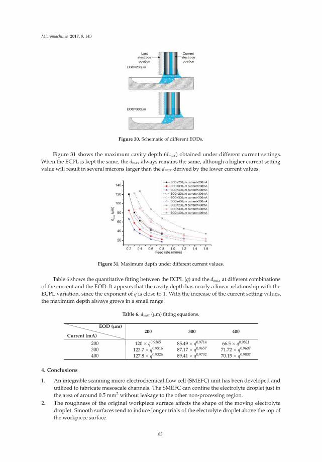
Micromachines 2017, 8, 143
Figure 30. Schematic of different EODs.
Figure 31 shows the maximum cavity depth (dmax) obtained under different current settings.When the ECPL is kept the same, the dmax always remains the same, although a higher current settingvalue will result in several microns larger than the dmax derived by the lower current values.
Figure 31. Maximum depth under different current values.
Table 6 shows the quantitative fitting between the ECPL (q) and the dmax at different combinationsof the current and the EOD. It appears that the cavity depth has nearly a linear relationship with theECPL variation, since the exponent of q is close to 1. With the increase of the current setting values,the maximum depth always grows in a small range.
Table 6. dmax (µm) fitting equations.
Current (mA)
EOD (µm)200 300 400
200 120 × q0.9365 85.49 × q0.9714 66.5 × q0.9821
300 123.7 × q0.9516 87.17 × q0.9657 71.72 × q0.9607
400 127.8 × q0.9326 89.41 × q0.9702 70.15 × q0.9807
4. Conclusions
1. An integrable scanning micro electrochemical flow cell (SMEFC) unit has been developed andutilized to fabricate mesoscale channels. The SMEFC can confine the electrolyte droplet just inthe area of around 0.5 mm2 without leakage to the other non-processing region.
2. The roughness of the original workpiece surface affects the shape of the moving electrolytedroplet. Smooth surfaces tend to induce longer trials of the electrolyte droplet above the top ofthe workpiece surface.
83

Micromachines 2017, 8, 143
3. Among all the geometrical parameters of the SMEFC configuration, the vacuum gap significantlyaffects the shape of the moving electrolyte droplet. A smaller vacuum gap tends to providea better control of the electrolyte droplet, which contributes to the consistency of the surfacemicrostructures. At the same level of the electric consumption per unit length, the channel depthmaintain the same on the whole, but suitable combinations of the current densities and feedrates can generate better surface quality and roughness. The concentration of the electrolyteinfluences the formation of the supersaturated layer and further affects the roughness. A highercurrent density, a smaller inter-electrode gap and a higher electrolyte concentration improve thecurrent efficiency.
4. As for the electrochemical milling by the SMEFC, the cavities machined with different electrodeoffset distances and different electric consumption per unit length have been compared.The electrode offset distance plays a significant role on the milling performance. Throughthe comparison of the cross-sectional profiles and SEM pictures, the electrode offset distance of300 µm together with the current of 400 mA is a better combination for obtaining a relativelysmooth bottom surface and a stable material removal rate. The removal depth can be adjusted bytuning the feed rate. A larger electrode offset distance and a higher current contribute to decreaseof the residues of the electrolyte crystallization.
5. In future research, a linear power supply can replace the switching power supply for a bettercurrent holding capability. The electrode with the outer diameter of 0.3 mm will also be utilizedto obtain smaller features. Multiple vision units will be installed at different angles to monitorand analyze the moving electrolyte droplet.
Acknowledgments: The authors would like to thank the China Scholarship Council (CSC) for providing ascholarship. Part of this research has been financed by the EC project Hi-Micro (Grant No. 314055) and MicroMAN(Grant No. 674801). The authors also would like to thank the technicians and Yansong Guo at the MechanicalEngineering Department of KU Leuven, for their assistance on component fabrication, and Shuigen Huang for theEDS analysis.
Author Contributions: Under the supervision of Dominiek Reynaerts and Jun Qian, Cheng Guo conducted themain research work, including hardware and software development of the experimental setup, design of theexperiments, analysis of the results, and writing the paper. Dominiek Reynaerts and Jun Qian have facilitated theexperiments, provided daily guidance and suggestions for this research work, and revised the paper.
Conflicts of Interest: The authors declare no conflict of interest. The founding sponsors had no role in the designof the study; in the collection, analyses, or interpretation of data; in the writing of the manuscript, and in thedecision to publish the results.
References
1. Lee, S.-J.; Lee, C.-Y.; Yang, K.-T.; Kuan, F.-H.; Lai, P.-H. Simulation and fabrication of micro-scaled flow
channels for metallic bipolar plates by the electrochemical micro-machining process. J. Power Sources 2008,
185, 1115–1121. [CrossRef]
2. Hung, J.-C.; Chang, C.-H.; Chiu, K.-C.; Lee, S.-J. Simulation-based fabrication of micro-helical grooves in a
hydrodynamic thrust bearing by using ecmm. Int. J. Adv. Manuf. Technol. 2013, 64, 813–820. [CrossRef]
3. Liu, G.X.; Zhang, Y.J.; Jiang, S.Z.; Liu, J.W.; Gyimah, G.K.; Luo, H.P. Investigation of pulse electrochemical sawing
machining of micro-inner annular groove on metallic tube. Int. J. Mach. Tools Manuf. 2016, 102, 22–34. [CrossRef]
4. Ryu, S.H. Eco-friendly ecm in citric acid electrolyte with microwire and microfoil electrodes. Int. J. Precis.
Eng. Manuf. 2015, 16, 233–239. [CrossRef]
5. Jia, L.; Xiaochen, J.; Di, Z. Electrochemical machining of multiple slots with low-frequency tool vibrations.
Procedia CIRP 2016, 42, 799–803. [CrossRef]
6. Liu, G.; Zhang, Y.; Deng, Y.; Wei, H.; Zhou, C.; Liu, J.; Luo, H. The tool design and experiments on pulse
electrochemical machining of micro channel arrays on metallic bipolar plate using multifunctional cathode.
Int. J. Adv. Manuf. Technol. 2017, 89, 407–416. [CrossRef]
7. Natsu, W.; Ikeda, T.; Kunieda, M. Generating complicated surface with electrolyte jet machining. Precis. Eng.
2007, 31, 33–39. [CrossRef]
84

Micromachines 2017, 8, 143
8. Hackert, M.; Meichsner, G.; Schubert, A. Generating micro geometries with air assisted jet electrochemical
machining. In Proceedings of the Euspen 10th Anniversary International Conference, Zurich, Switzerland,
18–22 May 2008; pp. 420–424.
9. Kai, S.; Sai, H.; Kunieda, M.; Izumi, H. Study on electrolyte jet cutting. Procedia CIRP 2012, 1, 627–632.
[CrossRef]
10. Kunieda, M.; Mizugai, K.; Watanabe, S.; Shibuya, N.; Iwamoto, N. Electrochemical micromachining using
flat electrolyte jet. CIRP Ann. Manuf. Technol. 2011, 60, 251–254. [CrossRef]
11. Hackert-Oschätzchen, M.; Meichsner, G.; Zinecker, M.; Martin, A.; Schubert, A. Micro machining with
continuous electrolytic free jet. Precis. Eng. 2012, 36, 612–619. [CrossRef]
12. Ghoshal, B.; Bhattacharyya, B. Investigation on profile of microchannel generated by electrochemical
micromachining. J. Mater. Process. Technol. 2015, 222, 410–421. [CrossRef]
13. Ghoshal, B.; Bhattacharyya, B. Electrochemical micromachining of microchannel using optimum scan feed
rate. J. Manuf. Process. 2016, 23, 258–268. [CrossRef]
14. Kim, B.H.; Ryu, S.H.; Choi, D.K.; Chu, C.N. Micro electrochemical milling. J. Micromech. Microeng. 2005,
15, 124. [CrossRef]
15. Zhang, Z.; Zhu, D.; Qu, N.; Wang, M. Theoretical and experimental investigation on electrochemical
micromachining. Microsyst. Technol. 2007, 13, 607–612. [CrossRef]
16. Shin, H.S.; Kim, B.H.; Chu, C.N. Analysis of the side gap resulting from micro electrochemical machining
with a tungsten wire and ultrashort voltage pulses. J. Micromech. Microeng. 2008, 18, 075009. [CrossRef]
17. Wang, S.; Zhu, D.; Zeng, Y.; Liu, Y. Micro wire electrode electrochemical cutting with low frequency and
small amplitude tool vibration. Int. J. Adv. Manuf. Technol. 2011, 53, 535–544. [CrossRef]
18. Liu, Z.; Nouraei, H.; Spelt, J.K.; Papini, M. Electrochemical slurry jet micro-machining of tungsten carbide
with a sodium chloride solution. Precis. Eng. 2015, 40, 189–198. [CrossRef]
19. Yuan, L.; Xu, J.; Zhao, J.; Zhang, H. Research on hybrid process of laser drilling with jet electrochemical
machining. J. Manuf. Sci. Eng. 2012, 134, 064502. [CrossRef]
20. Zhang, Z.; Cai, M.; Feng, Q.; Zeng, Y. Comparison of different laser-assisted electrochemical methods based
on surface morphology characteristics. Int. J. Adv. Manuf. Technol. 2014, 71, 565–571. [CrossRef]
21. Sakairi, M.; Sato, F.; Gotou, Y.; Fushimi, K.; Kikuchi, T.; Takahashi, H. Development of a novel microstructure
fabrication method with co-axial dual capillary solution flow type droplet cells and electrochemical
deposition. Electrochim. Acta 2008, 54, 616–622. [CrossRef]
22. Drensler, S.; Milenkovic, S.; Hassel, A.W. Microvials with tungsten nanowire arrays. J. Solid State Electrochem.
2014, 18, 2955–2961. [CrossRef]
23. Hu, J.-F.; Kuo, C.-L. Study on Micro Electrochemical Machining Using Coaxial for Gushing and Sucking
Method. Master’s Thesis, National Yunlin University of Science & Technology, Yunlin County, Taiwan, 2007.
24. Kuo, K.-Y.; Wu, K.-L.; Yang, C.-K.; Yan, B.-H. Wire electrochemical discharge machining (WECDM) of quartz
glass with titrated electrolyte flow. Int. J. Mach. Tools Manuf. 2013, 72, 50–57. [CrossRef]
25. Leroy, P.; Lassin, A.; Azaroual, M.; André, L. Predicting the surface tension of aqueous 1:1 electrolyte
solutions at high salinity. Geochim. Cosmochim. Acta 2010, 74, 5427–5442. [CrossRef]
26. Deconinck, D.; Hoogsteen, W.; Deconinck, J. A temperature dependent multi-ion model for time accurate
numerical simulation of the electrochemical machining process. Part III: Experimental validation. Electrochim.
Acta 2013, 103, 161–173. [CrossRef]
27. Rosenkranz, C.; Lohrengel, M.; Schultze, J. The surface structure during pulsed ecm of iron in NaNO3.
Electrochim. Acta 2005, 50, 2009–2016. [CrossRef]
28. Schubert, A.; Hackert-Oschätzchen, M.; Martin, A.; Winkler, S.; Kuhn, D.; Meichsner, G.; Zeidler, H.;
Edelmann, J. Generation of complex surfaces by superimposed multi-dimensional motion in electrochemical
machining. Procedia CIRP 2016, 42, 384–389. [CrossRef]
29. Martin, A.; Eckart, C.; Lehnert, N.; Hackert-Oschätzchen, M.; Schubert, A. Generation of defined surface
waviness on tungsten carbide by jet electrochemical machining with pulsed current. Procedia CIRP 2016, 45,
231–234. [CrossRef]
© 2017 by the authors. Licensee MDPI, Basel, Switzerland. This article is an open access
article distributed under the terms and conditions of the Creative Commons Attribution
(CC BY) license (http://creativecommons.org/licenses/by/4.0/).
85
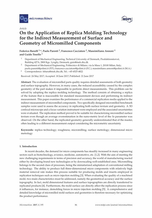
micromachines
Article
On the Application of Replica Molding Technologyfor the Indirect Measurement of Surface andGeometry of Micromilled Components
Federico Baruffi 1,*, Paolo Parenti 2, Francesco Cacciatore 2, Massimiliano Annoni 2
and Guido Tosello 1
1 Department of Mechanical Engineering, Technical University of Denmark, Produktionstorvet,Building 427A, 2800 Kgs. Lyngby, Denmark; [email protected]
2 Department of Mechanical Engineering, Politecnico di Milano, via la Masa 1, 20100 Milan, Italy;[email protected] (P.P.); [email protected] (F.C.); [email protected] (M.A.)
* Correspondence: [email protected]; Tel.: +45-4525-4822
Received: 24 May 2017; Accepted: 18 June 2017; Published: 21 June 2017
Abstract: The evaluation of micromilled parts quality requires detailed assessments of both geometryand surface topography. However, in many cases, the reduced accessibility caused by the complexgeometry of the part makes it impossible to perform direct measurements. This problem can besolved by adopting the replica molding technology. The method consists of obtaining a replicaof the feature that is inaccessible for standard measurement devices and performing its indirectmeasurement. This paper examines the performance of a commercial replication media applied to theindirect measurement of micromilled components. Two specifically designed micromilled benchmarksamples were used to assess the accuracy in replicating both surface texture and geometry. A 3Dconfocal microscope and a focus variation instrument were employed and the associated uncertaintieswere evaluated. The replication method proved to be suitable for characterizing micromilled surfacetexture even though an average overestimation in the nano-metric level of the Sa parameter wasobserved. On the other hand, the replicated geometry generally underestimated that of the master,often leading to a different measurement output considering the micrometric uncertainty.
Keywords: replica technology; roughness; micromilling; surface metrology; dimensional micrometrology
1. Introduction
In recent decades, the demand for micro components has steadily increased in many engineeringsectors such as biotechnology, avionics, medicine, automotive, etc. [1,2]. With the aim of meeting thenew challenging requirements in terms of precision and accuracy, the world of manufacturing reactedeither by developing brand new technologies or by downscaling well-established ones. Micromillingbelongs to the second class of processes, being the miniaturized adaptation of conventional millingtechnology. The ability to produce full three-dimensional micro components with relatively highmaterial removal rate makes this process suitable for producing molds and inserts employed inreplication techniques such as micro injection molding [3]. When evaluating the quality of a machinedmold, two main characteristics must be addressed, namely the geometrical accuracy and the surfacetopography. In fact, mold dimensional features and surface topographies are directly transferred toreplicated products [4]. Furthermore, the mold surface can directly affect the replication process sinceit influences, for instance, demolding forces in micro injection molding [5]. A comprehensive anddetailed knowledge of micromilled mold surfaces and geometries is therefore necessary for optimizingthe product performance.
Micromachines 2017, 8, 195 86 www.mdpi.com/journal/micromachines
Micromachines 2017, 8, 195
When dealing with micromilling, numerous phenomena, negligible for conventional milling,become significant. One of them is related to the minimum chip thickness effect [6]. When machiningwith chip thickness values comparable to the tool edge radius, effects such as plowing and elasticrecovery become dominant, causing a decrease of dimensional accuracy and an increase of surfaceroughness, in particular for soft-state metallic alloys [7].
At present, many dimensional and topographical measurement solutions can be applied tomicro components [8]. Among all of them, optical instruments are strongly emerging [9] because oftheir peculiar advantages. Firstly, their contact-less and non-destructive nature makes them suitablefor measuring soft and very small components: even a small force would in fact invalidate themeasurement or damage the sample. Furthermore, most optical measuring techniques allow an arealsurface characterization, which has more statistical significance in comparison to a profile one [10].Finally, they are potentially faster than typical contact instruments such as coordinate-measuringmachines (CMMs) and stylus profilometers. However, certain features, for instance micro holes ormicro cavities, are inaccessible for optical lenses, since an insufficient amount of light is reflectedback to the measuring objective. In other cases, samples may not physically fit under the microscope.Inaccessible features are typical in micro molds for injection molding applications, where high aspectratio features must often be replicated [11–13]. In such cases, new solutions must be employed toperform dimensional and surface measurements without adopting destructive inspections. Amongthem, replica molding technology is the most promising one. This method is based on the replicationof inaccessible features by means of casting-like soft polymeric media such as polydimethylsiloxane(PDMS) or two-component silicone polymers [4]. The common replication procedure simply consistsin casting the replication media over the component to be replicated. After the curing is completed,the replica is removed and then measured, providing and indirect quantitative information of the actualgeometry and surface. The use of such method is well-established in medical and dental fields [14,15]where specimens simply cannot be placed under a measuring instrument. It is also widely employedin non-destructive metallographic analysis of mechanical components [16,17]. For dimensional andsurface metrology tasks, replication kits based on a two-component polymer are nowadays widelyused [18,19]. Silicone based materials are usually employed, since they ensure almost no shrinkageover a wide range of curing temperature. When using these kits, the polymer and the curing agent areautomatically mixed in a disposable nozzle. A dispensing gun is utilized for directing the casting ofthe replication media. Tosello et al. [20] successively employed this method to monitor the tool wear ofa mold for Fresnel lenses production presenting micro structures with a height of 23 µm.
In recent decades, few research papers investigated the replication performance of fast replicationmedia used in indirect metrology tasks. Madsen et al. [21] studied the shrinkage of a PDMS materialutilized for measuring nano-metric geometries. The authors considered several mixing ratios and curingtemperature levels and investigated the repeatability of the process through repeated replicas. The authorsconcluded that the utilized PDMS shrinks linearly between 1% and 3 %, leading to dimensions thatare smaller than the ones of the replicated master. In a recent paper, Goodall et al. [22] analyzed theaccuracy and precision of seven different silicone based replication media utilized for quantitative surfacetexture characterization. Two masters, one smooth and one rough lower jaw teeth, were replicated.Most of the areal surface texture parameters and fractal parameterization were employed to carry outcomparisons. It was found that low viscosity media generally achieve higher accuracy and precision.However, the authors highlighted a need for standardization, since results from different impressionmedia were not comparable. Finally, Gasparin et al. [23] investigated the surface texture replicationperformance of three replication media (one hard and two soft). Two calibrated roughness standardswere used as masters. Measurements were performed with optical and tactile instruments. A replicationdegree up to 96% was reached, proving that the measured deviations fell inside the uncertainty range.Since the nominal Ra value of the measured standard was 500 nm, the authors’ considerations cannot bedirectly extended to micromilled surfaces, which are usually smoother (in most applications, Ra rangesbetween 50 nm and 250 nm [24–27] on both flat and free-form parts).
87
Micromachines 2017, 8, 195
Despite several approaches have been proposed in literature [28,29], the use of surface topographyprediction models in industrial micromilling applications is still extremely limited. This is due to thelack of robustness that the models show with respect to the variability of the material characteristics,tool micro-geometry and tool wear. Therefore, the measurement of micromilled surface after machiningrepresents the standard practice that machinists still adopt for verifying the cutting process results.The replication and the following indirect measurement are thus the preferable solution for characterizingthe surface topography of inaccessible micromilled features.
At present, the literature still lacks a study focused on the performance verification of a replicaprocedure specifically applied to micromilled components.
The aim of this paper is to evaluate the performance of a commercial silicone replication media(RepliSet [19], Struers®, Ballerup, Denmark) in the indirect measurement of micromilled surfacesand geometries made from mold steel. In order to accomplish this, a quantitative comparisonbetween micromilled masters and their replicas was carried out. In particular, the performancein replicating both surface topography and geometry was assessed separately using two differentbenchmark samples.
2. Materials and Methods
In order to assess the surface replication fidelity of the silicone media, two different samples weredesigned and then machined.
The first one was used to assess the replication performance related to indirect surface roughnessmeasurements. Different benchmark surfaces were machined and then replicated. Micro-roughedand micro-finished surfaces were obtained by varying the radial depth of cut. Two materials weremilled: AISI 440 hardened (AISI 440 H, hardness = 60 HRC) and AISI 440 annealed (AISI 440 A,hardness = 18 HRC). These two stainless steels represent a suitable choice for mold manufacturing andare expected to produce different surface topographies in relation to the specific material characteristics,as for instance hardness, grain size and specific cutting force. In particular, being AISI 440 A in a softstate, the risk of plowing is certainly higher than for the harder AISI 440 H [7].
The second sample was used to investigate the replication capability related to indirect geometricalmeasurements. Five micromilled pockets were produced on the same two aforementioned materialsand successively replicated. The geometry of the pockets was varied in order to assess the replicationfidelity of the silicone media at different penetration depths.
2.1. Micromilled Surfaces
The consideration of surface topography is the first step for the assessment of any replicationmethod. In micromilling surface generation, several factors affect the final surface topography.In particular, milling process parameters, milling strategy and the geometry of the adopted toolall play an important role. In this study, three typologies of micromilled surface were produced on boththe materials. A coated WC Round End Mill (Mitsubishi Materials Corporation, Tokyo, Japan) (2 flutes,diameter = 1 mm, Corner Radius = 0.1 mm and cutting edge radius = 6 µm) was used for the tests onan ultra-high precision KERN Evo micromilling machine. Table 1 shows the cutting parameters for thethree machined surfaces.
Table 1. Cutting parameters for the three machined surfaces.
Cutting Parameter S1 S2 S3
ae/DC 100% (full slot) 30% (overlapped) 30% (finished)ap/µm 50 50 50
vc/(m/min) 100 100 100f z/µm 12.5 12.5 12.5
88
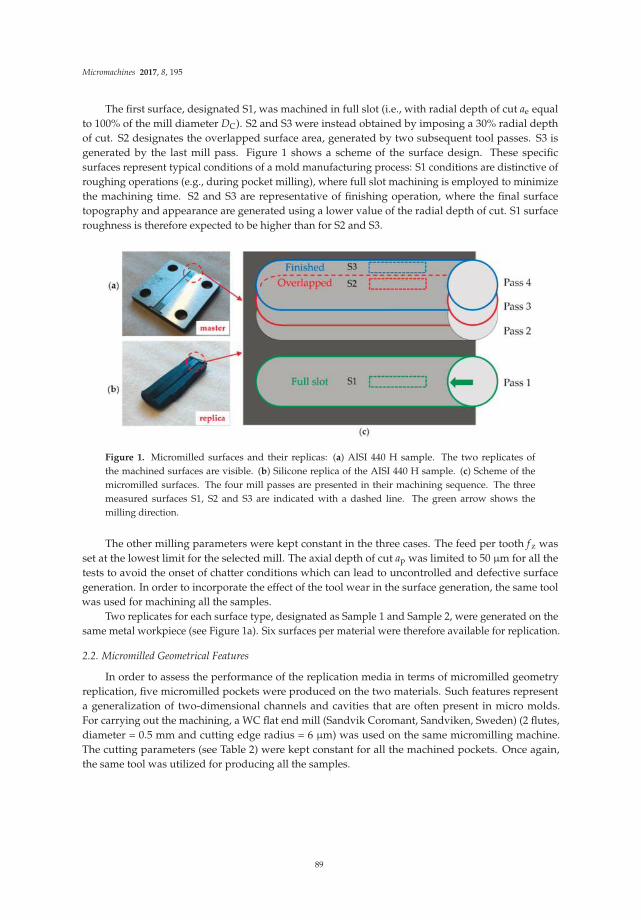
Micromachines 2017, 8, 195
The first surface, designated S1, was machined in full slot (i.e., with radial depth of cut ae equalto 100% of the mill diameter DC). S2 and S3 were instead obtained by imposing a 30% radial depthof cut. S2 designates the overlapped surface area, generated by two subsequent tool passes. S3 isgenerated by the last mill pass. Figure 1 shows a scheme of the surface design. These specificsurfaces represent typical conditions of a mold manufacturing process: S1 conditions are distinctive ofroughing operations (e.g., during pocket milling), where full slot machining is employed to minimizethe machining time. S2 and S3 are representative of finishing operation, where the final surfacetopography and appearance are generated using a lower value of the radial depth of cut. S1 surfaceroughness is therefore expected to be higher than for S2 and S3.
Figure 1. Micromilled surfaces and their replicas: (a) AISI 440 H sample. The two replicates ofthe machined surfaces are visible. (b) Silicone replica of the AISI 440 H sample. (c) Scheme of themicromilled surfaces. The four mill passes are presented in their machining sequence. The threemeasured surfaces S1, S2 and S3 are indicated with a dashed line. The green arrow shows themilling direction.
The other milling parameters were kept constant in the three cases. The feed per tooth f z wasset at the lowest limit for the selected mill. The axial depth of cut ap was limited to 50 µm for all thetests to avoid the onset of chatter conditions which can lead to uncontrolled and defective surfacegeneration. In order to incorporate the effect of the tool wear in the surface generation, the same toolwas used for machining all the samples.
Two replicates for each surface type, designated as Sample 1 and Sample 2, were generated on thesame metal workpiece (see Figure 1a). Six surfaces per material were therefore available for replication.
2.2. Micromilled Geometrical Features
In order to assess the performance of the replication media in terms of micromilled geometryreplication, five micromilled pockets were produced on the two materials. Such features representa generalization of two-dimensional channels and cavities that are often present in micro molds.For carrying out the machining, a WC flat end mill (Sandvik Coromant, Sandviken, Sweden) (2 flutes,diameter = 0.5 mm and cutting edge radius = 6 µm) was used on the same micromilling machine.The cutting parameters (see Table 2) were kept constant for all the machined pockets. Once again,the same tool was utilized for producing all the samples.
89
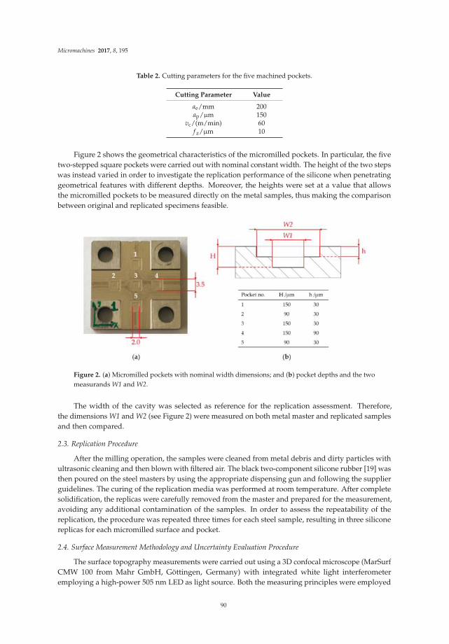
Micromachines 2017, 8, 195
Table 2. Cutting parameters for the five machined pockets.
Cutting Parameter Value
ae/mm 200ap/µm 150
vc/(m/min) 60f z/µm 10
Figure 2 shows the geometrical characteristics of the micromilled pockets. In particular, the fivetwo-stepped square pockets were carried out with nominal constant width. The height of the two stepswas instead varied in order to investigate the replication performance of the silicone when penetratinggeometrical features with different depths. Moreover, the heights were set at a value that allowsthe micromilled pockets to be measured directly on the metal samples, thus making the comparisonbetween original and replicated specimens feasible.
Figure 2. (a) Micromilled pockets with nominal width dimensions; and (b) pocket depths and the twomeasurands W1 and W2.
The width of the cavity was selected as reference for the replication assessment. Therefore,the dimensions W1 and W2 (see Figure 2) were measured on both metal master and replicated samplesand then compared.
2.3. Replication Procedure
After the milling operation, the samples were cleaned from metal debris and dirty particles withultrasonic cleaning and then blown with filtered air. The black two-component silicone rubber [19] wasthen poured on the steel masters by using the appropriate dispensing gun and following the supplierguidelines. The curing of the replication media was performed at room temperature. After completesolidification, the replicas were carefully removed from the master and prepared for the measurement,avoiding any additional contamination of the samples. In order to assess the repeatability of thereplication, the procedure was repeated three times for each steel sample, resulting in three siliconereplicas for each micromilled surface and pocket.
2.4. Surface Measurement Methodology and Uncertainty Evaluation Procedure
The surface topography measurements were carried out using a 3D confocal microscope (MarSurfCMW 100 from Mahr GmbH, Göttingen, Germany) with integrated white light interferometeremploying a high-power 505 nm LED as light source. Both the measuring principles were employed
90
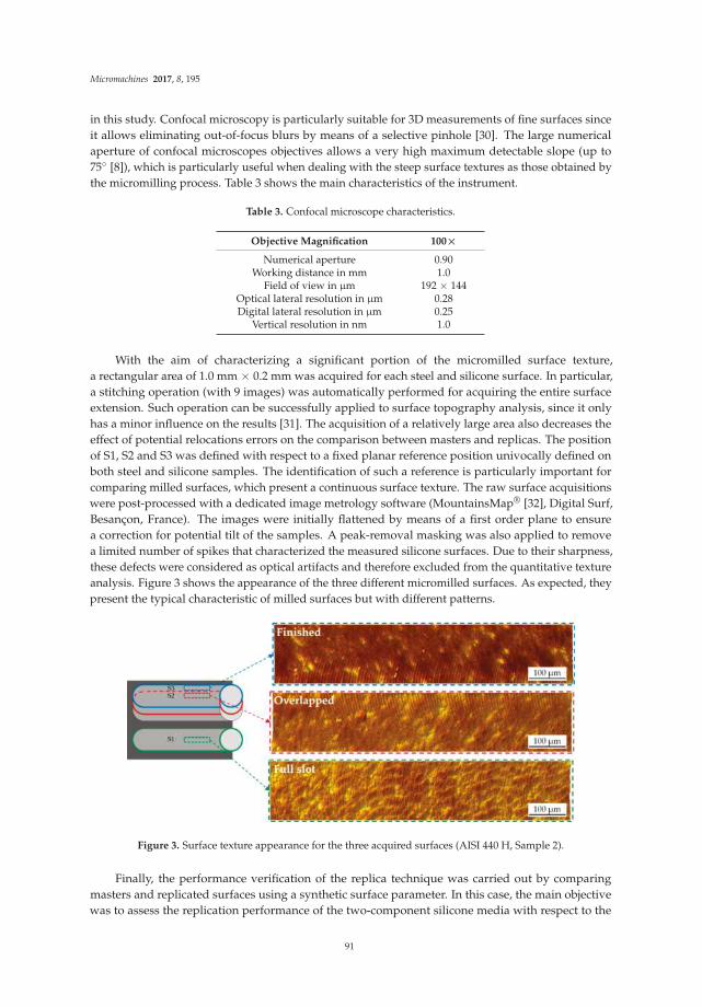
Micromachines 2017, 8, 195
in this study. Confocal microscopy is particularly suitable for 3D measurements of fine surfaces sinceit allows eliminating out-of-focus blurs by means of a selective pinhole [30]. The large numericalaperture of confocal microscopes objectives allows a very high maximum detectable slope (up to75◦ [8]), which is particularly useful when dealing with the steep surface textures as those obtained bythe micromilling process. Table 3 shows the main characteristics of the instrument.
Table 3. Confocal microscope characteristics.
Objective Magnification 100×
Numerical aperture 0.90Working distance in mm 1.0
Field of view in µm 192 × 144Optical lateral resolution in µm 0.28Digital lateral resolution in µm 0.25
Vertical resolution in nm 1.0
With the aim of characterizing a significant portion of the micromilled surface texture,a rectangular area of 1.0 mm × 0.2 mm was acquired for each steel and silicone surface. In particular,a stitching operation (with 9 images) was automatically performed for acquiring the entire surfaceextension. Such operation can be successfully applied to surface topography analysis, since it onlyhas a minor influence on the results [31]. The acquisition of a relatively large area also decreases theeffect of potential relocations errors on the comparison between masters and replicas. The positionof S1, S2 and S3 was defined with respect to a fixed planar reference position univocally defined onboth steel and silicone samples. The identification of such a reference is particularly important forcomparing milled surfaces, which present a continuous surface texture. The raw surface acquisitionswere post-processed with a dedicated image metrology software (MountainsMap® [32], Digital Surf,Besançon, France). The images were initially flattened by means of a first order plane to ensurea correction for potential tilt of the samples. A peak-removal masking was also applied to removea limited number of spikes that characterized the measured silicone surfaces. Due to their sharpness,these defects were considered as optical artifacts and therefore excluded from the quantitative textureanalysis. Figure 3 shows the appearance of the three different micromilled surfaces. As expected, theypresent the typical characteristic of milled surfaces but with different patterns.
Figure 3. Surface texture appearance for the three acquired surfaces (AISI 440 H, Sample 2).
Finally, the performance verification of the replica technique was carried out by comparingmasters and replicated surfaces using a synthetic surface parameter. In this case, the main objectivewas to assess the replication performance of the two-component silicone media with respect to the
91
Micromachines 2017, 8, 195
vertical profile development, since, given its nano-metric range, it is most critical to replicate. Therefore,the arithmetical mean height Sa was computed for each surface and then utilized as the parameterof comparison. This parameter, according to the ISO 25178-2 standard [33], gives indication aboutthe average areal surface roughness of the surface, being the analogous of Ra that is used to describeprofile measurements. Sa was chosen as indicator since it is only slightly influenced by local defects oroptical artifacts, and therefore is suitable for a carrying out a general comparison between two surfaces.No cutoff filter was applied before calculating Sa. In this way, the performance replication throughoutthe entire spatial frequency domain was investigated.
To verify the quality of the measurements, an uncertainty evaluation was carried out.The measurement uncertainty U is a parameter associated with the results of a measurement thatcharacterizes the dispersion of the values that could be reasonably be attributed to the measurand [34].It is of paramount importance to determine this parameter and to include it in the evaluation of thereplication capability, since, at the nano-scale, the variations due to replication process, instrumentaccuracy and measurement repeatability are in the same order of magnitude [4]. The uncertaintybudget of the Sa measurements on the metal and silicone samples was estimated following ISO15530-3 [35]. Although this method was conceived for CMM measurements, its principle can besuccessfully applied to optical measurements [23], allowing to avoid some of the complications thata full uncertainty estimation would introduce [36]. Such an approach is based on the substitutionmethod, which allows estimating the instrument uncertainty by repeated measurements on a calibratedartifact sharing similar characteristic with the actual measurand. In this particular case, a calibratedroughness artifact (nominal value: Ra = 480 nm) was employed for this task. The measurementuncertainty related to surface roughness measurements when using the confocal microscope uCONF
was calculated as follows:uCONF =
√
u2cal + u2
p + u2res,CONF (1)
where ucal is the standard calibration uncertainty of the roughness standard; up represents the standarduncertainty related to the measurement procedure and is calculated as standard deviation of fifteenrepeated measurements on the calibrated standard; and ures,CONF is the resolution uncertainty relatedto the declared 1 nm vertical resolution of the confocal microscope. The uncertainty contributionintroduced by the thermal deformation of the samples was neglected since the measurements wereperformed inside a metrologic laboratory with a 20 ◦C ± 0.5 ◦C controlled temperature.
In order to evaluate the uncertainty related to the measurements of the actual measurands,one more source of uncertainty was taken into account: uSa, mill, the standard deviation of tenrepeated Sa measurements on the micromilled samples and on their replicas. Therefore, the expandeduncertainty of surface roughness measurement of the micromilled surfaces is calculated as:
USa = k×√
u2CONF + u2
Sa, mill (2)
where k is the coverage factor, equal to 2 for a 95% confidence interval. In order to characterize theuncertainty of both masters and replicas, uSa, mill was calculated for the three materials involved in thestudy. Table 4 presents the uncertainty budget.
Table 4. Uncertainty contributions for the Sa roughness measurements on the masters andreplicated surfaces.
Uncertainty Contribution AISI 440 H AISI 440 A Silicone
ucal/nm 11.0 11.0 11.0up/nm 2.1 2.1 2.1
ures,CONF/nm 0.3 0.3 0.3uCONF/nm 11.2 11.2 11.2uSa, mill/nm 3.7 3.9 4.7
USa/nm 24 24 24
92
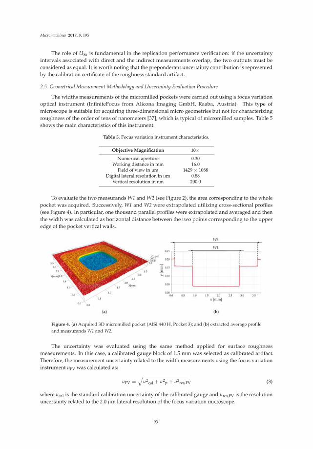
Micromachines 2017, 8, 195
The role of USa is fundamental in the replication performance verification: if the uncertaintyintervals associated with direct and the indirect measurements overlap, the two outputs must beconsidered as equal. It is worth noting that the preponderant uncertainty contribution is representedby the calibration certificate of the roughness standard artifact.
2.5. Geometrical Measurement Methodology and Uncertainty Evaluation Procedure
The widths measurements of the micromilled pockets were carried out using a focus variationoptical instrument (InfiniteFocus from Alicona Imaging GmbH, Raaba, Austria). This type ofmicroscope is suitable for acquiring three-dimensional micro geometries but not for characterizingroughness of the order of tens of nanometers [37], which is typical of micromilled samples. Table 5shows the main characteristics of this instrument.
Table 5. Focus variation instrument characteristics.
Objective Magnification 10×
Numerical aperture 0.30Working distance in mm 16.0
Field of view in µm 1429 × 1088Digital lateral resolution in µm 0.88
Vertical resolution in nm 200.0
To evaluate the two measurands W1 and W2 (see Figure 2), the area corresponding to the wholepocket was acquired. Successively, W1 and W2 were extrapolated utilizing cross-sectional profiles(see Figure 4). In particular, one thousand parallel profiles were extrapolated and averaged and thenthe width was calculated as horizontal distance between the two points corresponding to the upperedge of the pocket vertical walls.
Figure 4. (a) Acquired 3D micromilled pocket (AISI 440 H, Pocket 3); and (b) extracted average profileand measurands W1 and W2.
The uncertainty was evaluated using the same method applied for surface roughnessmeasurements. In this case, a calibrated gauge block of 1.5 mm was selected as calibrated artifact.Therefore, the measurement uncertainty related to the width measurements using the focus variationinstrument uFV was calculated as:
uFV =√
u2cal + u2
p + u2res,FV (3)
where ucal is the standard calibration uncertainty of the calibrated gauge and ures,FV is the resolutionuncertainty related to the 2.0 µm lateral resolution of the focus variation microscope.
93
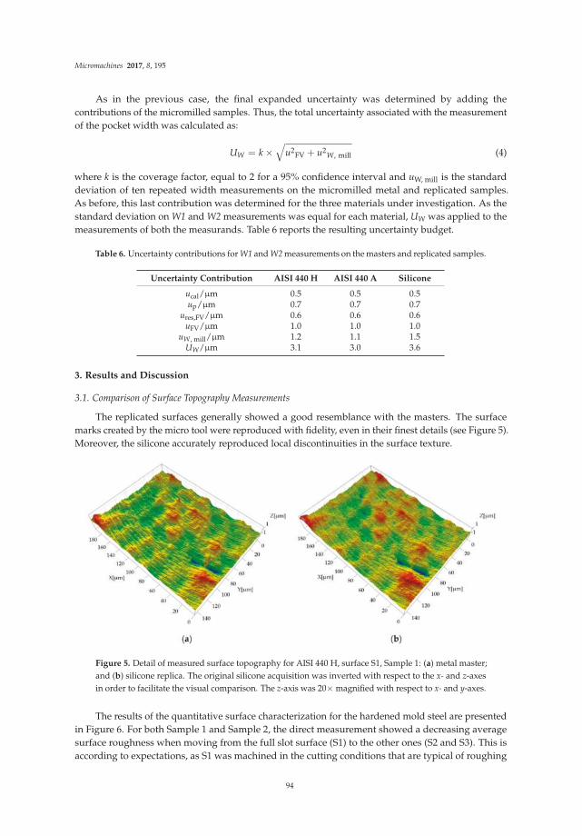
Micromachines 2017, 8, 195
As in the previous case, the final expanded uncertainty was determined by adding thecontributions of the micromilled samples. Thus, the total uncertainty associated with the measurementof the pocket width was calculated as:
UW = k ×√
u2FV + u2
W, mill (4)
where k is the coverage factor, equal to 2 for a 95% confidence interval and uW, mill is the standarddeviation of ten repeated width measurements on the micromilled metal and replicated samples.As before, this last contribution was determined for the three materials under investigation. As thestandard deviation on W1 and W2 measurements was equal for each material, UW was applied to themeasurements of both the measurands. Table 6 reports the resulting uncertainty budget.
Table 6. Uncertainty contributions for W1 and W2 measurements on the masters and replicated samples.
Uncertainty Contribution AISI 440 H AISI 440 A Silicone
ucal/µm 0.5 0.5 0.5up/µm 0.7 0.7 0.7
ures,FV/µm 0.6 0.6 0.6uFV/µm 1.0 1.0 1.0
uW, mill/µm 1.2 1.1 1.5UW/µm 3.1 3.0 3.6
3. Results and Discussion
3.1. Comparison of Surface Topography Measurements
The replicated surfaces generally showed a good resemblance with the masters. The surfacemarks created by the micro tool were reproduced with fidelity, even in their finest details (see Figure 5).Moreover, the silicone accurately reproduced local discontinuities in the surface texture.
Figure 5. Detail of measured surface topography for AISI 440 H, surface S1, Sample 1: (a) metal master;and (b) silicone replica. The original silicone acquisition was inverted with respect to the x- and z-axesin order to facilitate the visual comparison. The z-axis was 20× magnified with respect to x- and y-axes.
The results of the quantitative surface characterization for the hardened mold steel are presentedin Figure 6. For both Sample 1 and Sample 2, the direct measurement showed a decreasing averagesurface roughness when moving from the full slot surface (S1) to the other ones (S2 and S3). This isaccording to expectations, as S1 was machined in the cutting conditions that are typical of roughing
94

Micromachines 2017, 8, 195
operations. In general, Sa measured on the master surfaces ranged between 55 nm and 96 nm. A certainroughness variability was observed between the direct measurements of the two samples. In particular,Sample 1 presented an 11 nm to 18 nm larger Sa compared to Sample 2. This variability is due to themicromilling process itself, since the surfaces were machined in the same cutting conditions on thetwo samples. In comparison to the direct measurement, the three replicas always presented a largerSa. However, considering the measurement uncertainty, direct and indirect measurements provided,in all the cases, the same Sa values. In fact, the uncertainty intervals overlap, making the measurementoutput equal from a metrological point of view. The standard deviations among the three siliconereplicas range between 3 nm and 11 nm, demonstrating good repeatability of the replication procedure.Moreover, taking into account the measurement uncertainty, the replication procedure always providedconsistent Sa results.
Figure 6. Sa values measured on master (green) and replicated (red) surfaces for AISI 440 H. The resultsfor the three surfaces S1 (left), S2 (middle) and S3 (right) are shown: (a) Sample 1; and (b) Sample 2.The error bars indicate the expanded uncertainty USa.
The results of the Sa measurements for the AISI 440 A are shown in Figure 7. In this case, S1 andS2 were produced with similar Sa roughness values (ranging between 61 nm and 74 nm for the twosamples), while S3 had a significantly higher value of around 200 nm. This is contrary to expectations,as S3 was machined with the same radial depth of cut of S2. This unexpected increase of surfaceroughness was caused by the presence of plowing: for AISI 440 A, the last micromilling pass generatedplowed marks on the surface, which diminished the surface quality (see Figure 8). This event happenedonly for S3 because the material accumulated on the tool during the first three passes (see Figure 1)leading to an increase of surface roughness [7] during the last pass. The softness of the annealedmaterial is the most probable reason for this phenomenon. As for the previous material, a certainvariability between Sample 1 and Sample 2 was observed. When comparing direct and indirectmeasurements, the replication process again introduced an average overestimation of the surfaceroughness of the master. However, as for the hardened material, the uncertainty intervals of direct andindirect measurements overlap in almost all cases, except for Replica 3 of S1, Sample 2 and Replica 2 ofS3, Sample 1. The replication process is once again very repeatable: the three different replicas always
95
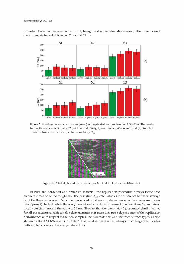
Micromachines 2017, 8, 195
provided the same measurements output, being the standard deviations among the three indirectmeasurements included between 7 nm and 15 nm.
Figure 7. Sa values measured on master (green) and replicated (red) surfaces for AISI 440 A. The resultsfor the three surfaces S1 (left), S2 (middle) and S3 (right) are shown: (a) Sample 1; and (b) Sample 2.The error bars indicate the expanded uncertainty USa.
Figure 8. Detail of plowed marks on surface S3 of AISI 440 A material, Sample 2.
In both the hardened and annealed material, the replication procedure always introducedan overestimation of the roughness. The deviation ∆Sa, calculated as the difference between averageSa of the three replicas and Sa of the master, did not show any dependence on the master roughness(see Figure 9). In fact, while the roughness of metal surfaces increased, the deviation ∆Sa remainedmostly constant around the value of 24 nm. The fact that the parameter ∆Sa assumed similar valuesfor all the measured surfaces also demonstrates that there was not a dependence of the replicationperformance with respect to the two samples, the two materials and the three surface types, as alsoshown by the ANOVA results in Table 7. The p-values were in fact always much larger than 5% forboth single factors and two-ways interactions.
96
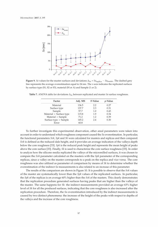
Micromachines 2017, 8, 195
Figure 9. Sa values for the master surfaces and deviations ∆Sa = Sareplica − Samaster. The dashed greyline represents the average overestimation equal to 24 nm. The x-axis indicates the replicated surfacesby surface type (S1, S2 or S3), material (H or A) and Sample (1 or 2).
Table 7. ANOVA table for deviations ∆Sa between replicated and master Sa surface roughness.
Factor Adj. MS F-Value p-Value
Material 136.5 2.2 0.27Surface type 137.7 2.3 0.31
Sample 57.7 1.0 0.43Material × Surface type 115.8 1.9 0.34
Material × Sample 71.2 1.2 0.39Surface type × Sample 145.2 2.4 0.30
Error 60.8
To further investigate this experimental observation, other areal parameters were taken intoaccount in order to understand which roughness component caused the Sa overestimation. In particular,the functional parameters Svk, Spk and Sk were calculated for masters and replicas and then compared.Svk is defined as the reduced dale height, and it provides an average indication of the valleys depthbelow the core roughness [33]. Spk is the reduced peak height and represents the mean height of peaksabove the core surface [33]. Finally, Sk is used to characterize the core surface roughness [33]. In orderto analyze how the silicone media replicated the valleys of the micromilled surfaces, it was chosen tocompare the Svk parameter calculated on the masters with the Spk parameter of the correspondingreplicas, since a valley on the master corresponds to a peak on the replica and vice versa. The coreroughness was also utilized as parameter of comparison by means of Sk to determine whether theoverestimation of the indirect Sa measurements is also related to an increase of this parameter.
The results of the comparison are shown in Figure 10. It is possible to observe that the Svk valuesof the master are systematically lower than the Spk values of the replicated surfaces. In particular,the Spk of the replicas is on average 60% higher than the Svk of the masters. This clearly demonstratesthat the replication procedure generated surfaces having peaks that are higher than the valleys ofthe master. The same happens for Sk: the indirect measurements provided an average 63% higherlevel of Sk for all the produced surfaces, indicating that the core roughness is also increased after thereplication procedure. Therefore, the Sa overestimation introduced by the indirect measurements iscaused by two distinct phenomena: the increase of the height of the peaks with respect to depths ofthe valleys and the increase of the core roughness.
97

Micromachines 2017, 8, 195
Figure 10. Functional roughness parameters calculated on master (blue) and replicated (green) samples:(a) Svk and Spk values for master and replicas respectively; and (b) Sk values. The interval barsindicate the standard deviations calculated among the three replicas. The x-axis indicates surface type(S1, S2 or S3), material (H or A) and Sample (1 or 2).
This phenomenon is probably generated during the demolding phase of the replica.The two-component silicone during solidification penetrates in the master surface valleys, replicatingthe surface topography (see Figure 5). When the solidified replica is manually removed, the siliconesticks to the deepest points of the surface valleys due to their very small width, making its removalmore difficult than in other areas. Therefore, it appears that manual removal causes a nano-metricstretch perpendicular to the average plane of the surface, which results in the observed increase ofboth dale height and core roughness. This also explains why the overestimation is almost constant(see Figure 9): the manual removal acts as external factor, and it does not depend on the experimentalvariables. Another evidence is given by the Kurtosis parameter Sku [33], which provides a quantitativeevaluation of the sharpness of the roughness profile. The replicated surfaces had, on average, a 23%higher Sku value, demonstrating that they have a sharper profile than the masters, as a consequence ofthe stretch induced by the manual removal.
3.2. Comparison of Geometrical Measurements
The steel micromilled pockets and their silicone replicas had a very similar shape. In particular,the replicas were able to accurately reproduce the geometry of the vertical walls, since no trace ofany tilt due to the shrinkage of the polymer was present. With regard to the steps of the pockets,a not-perfect perpendicularity of the silicone pockets with respect to the vertical axis was sometimesobserved, as shown in Figure 11 where Replica 3 presents a slightly tilted intermediate horizontal line.This micrometric deformation does not affect the width measurements.
98
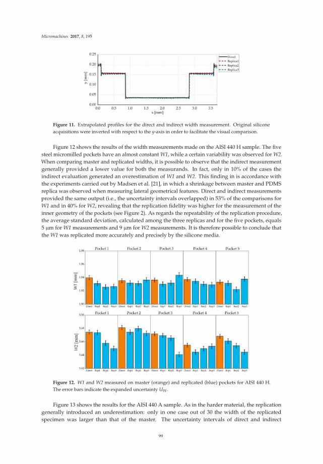
Micromachines 2017, 8, 195
Figure 11. Extrapolated profiles for the direct and indirect width measurement. Original siliconeacquisitions were inverted with respect to the y-axis in order to facilitate the visual comparison.
Figure 12 shows the results of the width measurements made on the AISI 440 H sample. The fivesteel micromilled pockets have an almost constant W1, while a certain variability was observed for W2.When comparing master and replicated widths, it is possible to observe that the indirect measurementgenerally provided a lower value for both the measurands. In fact, only in 10% of the cases theindirect evaluation generated an overestimation of W1 and W2. This finding in is accordance withthe experiments carried out by Madsen et al. [21], in which a shrinkage between master and PDMSreplica was observed when measuring lateral geometrical features. Direct and indirect measurementsprovided the same output (i.e., the uncertainty intervals overlapped) in 53% of the comparisons forW1 and in 40% for W2, revealing that the replication fidelity was higher for the measurement of theinner geometry of the pockets (see Figure 2). As regards the repeatability of the replication procedure,the average standard deviation, calculated among the three replicas and for the five pockets, equals5 µm for W1 measurements and 9 µm for W2 measurements. It is therefore possible to conclude thatthe W1 was replicated more accurately and precisely by the silicone media.
Figure 12. W1 and W2 measured on master (orange) and replicated (blue) pockets for AISI 440 H.The error bars indicate the expanded uncertainty UW.
Figure 13 shows the results for the AISI 440 A sample. As in the harder material, the replicationgenerally introduced an underestimation: only in one case out of 30 the width of the replicatedspecimen was larger than that of the master. The uncertainty intervals of direct and indirect
99
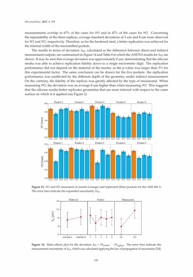
Micromachines 2017, 8, 195
measurements overlap in 67% of the cases for W1 and in 47% of the cases for W2. Concerningthe repeatability of the three replicas, average standard deviations of 3 µm and 8 µm were observedfor W1 and W2, respectively. Therefore, as for the hardened steel, a better replication was achieved forthe internal width of the micromilled pockets.
The results in terms of deviation ∆W, calculated as the difference between direct and indirectmeasurement outputs, are summarized in Figure 14 and Table 8 in which the ANOVA results for ∆W areshown. It may be seen that average deviation was approximately 8 µm, demonstrating that the siliconemedia was able to achieve replication fidelity down to a single micrometer digit. The replicationperformance did not depend on the material of the master, as the p-value was larger than 5% forthis experimental factor. The same conclusion can be drawn for the five pockets: the replicationperformance was unaffected by the different depth of the geometry under indirect measurement.On the contrary, the fidelity of the replicas was greatly affected by the type of measurand. Whenmeasuring W2, the deviation was on average 8 µm higher than when measuring W1. This suggeststhat the silicone media better replicates geometries that are more internal with respect to the outersurface on which it is applied (see Figure 2).
Figure 13. W1 and W2 measured on master (orange) and replicated (blue) pockets for the AISI 440 A.The error bars indicate the expanded uncertainty UW.
Figure 14. Main effects plot for the deviation ∆W = Wmaster − Wreplica. The error bars indicate themeasurement uncertainty of ∆W, which was calculated applying the law of propagation of uncertainty [34].
100
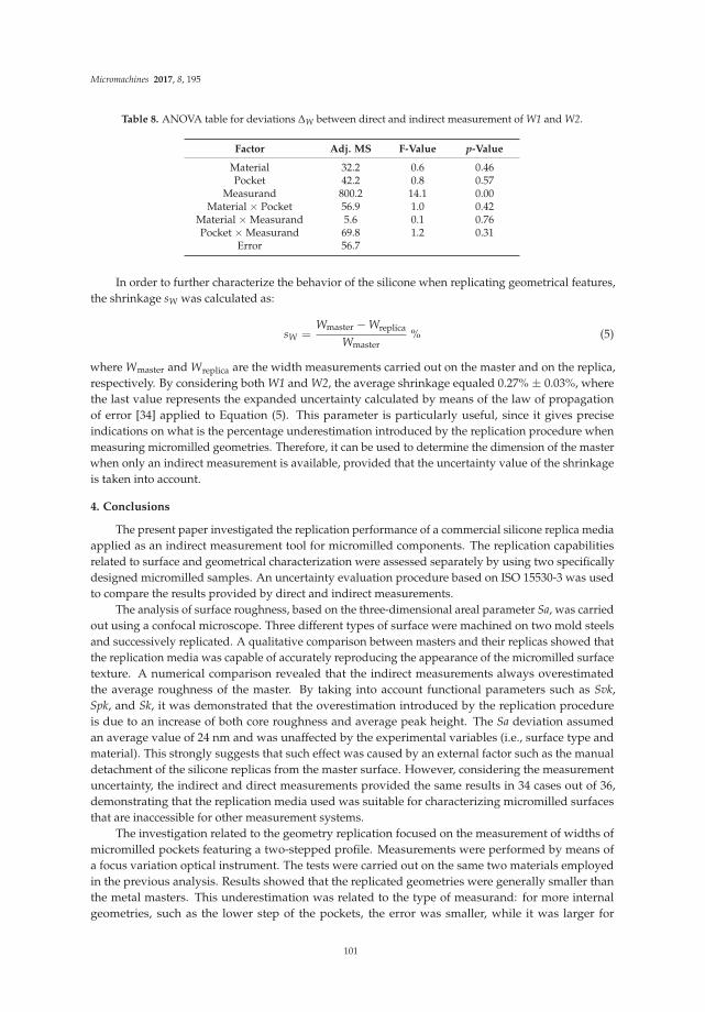
Micromachines 2017, 8, 195
Table 8. ANOVA table for deviations ∆W between direct and indirect measurement of W1 and W2.
Factor Adj. MS F-Value p-Value
Material 32.2 0.6 0.46Pocket 42.2 0.8 0.57
Measurand 800.2 14.1 0.00Material × Pocket 56.9 1.0 0.42
Material × Measurand 5.6 0.1 0.76Pocket × Measurand 69.8 1.2 0.31
Error 56.7
In order to further characterize the behavior of the silicone when replicating geometrical features,the shrinkage sW was calculated as:
sW =Wmaster − Wreplica
Wmaster% (5)
where Wmaster and Wreplica are the width measurements carried out on the master and on the replica,respectively. By considering both W1 and W2, the average shrinkage equaled 0.27% ± 0.03%, wherethe last value represents the expanded uncertainty calculated by means of the law of propagationof error [34] applied to Equation (5). This parameter is particularly useful, since it gives preciseindications on what is the percentage underestimation introduced by the replication procedure whenmeasuring micromilled geometries. Therefore, it can be used to determine the dimension of the masterwhen only an indirect measurement is available, provided that the uncertainty value of the shrinkageis taken into account.
4. Conclusions
The present paper investigated the replication performance of a commercial silicone replica mediaapplied as an indirect measurement tool for micromilled components. The replication capabilitiesrelated to surface and geometrical characterization were assessed separately by using two specificallydesigned micromilled samples. An uncertainty evaluation procedure based on ISO 15530-3 was usedto compare the results provided by direct and indirect measurements.
The analysis of surface roughness, based on the three-dimensional areal parameter Sa, was carriedout using a confocal microscope. Three different types of surface were machined on two mold steelsand successively replicated. A qualitative comparison between masters and their replicas showed thatthe replication media was capable of accurately reproducing the appearance of the micromilled surfacetexture. A numerical comparison revealed that the indirect measurements always overestimatedthe average roughness of the master. By taking into account functional parameters such as Svk,Spk, and Sk, it was demonstrated that the overestimation introduced by the replication procedureis due to an increase of both core roughness and average peak height. The Sa deviation assumedan average value of 24 nm and was unaffected by the experimental variables (i.e., surface type andmaterial). This strongly suggests that such effect was caused by an external factor such as the manualdetachment of the silicone replicas from the master surface. However, considering the measurementuncertainty, the indirect and direct measurements provided the same results in 34 cases out of 36,demonstrating that the replication media used was suitable for characterizing micromilled surfacesthat are inaccessible for other measurement systems.
The investigation related to the geometry replication focused on the measurement of widths ofmicromilled pockets featuring a two-stepped profile. Measurements were performed by means ofa focus variation optical instrument. The tests were carried out on the same two materials employedin the previous analysis. Results showed that the replicated geometries were generally smaller thanthe metal masters. This underestimation was related to the type of measurand: for more internalgeometries, such as the lower step of the pockets, the error was smaller, while it was larger for
101
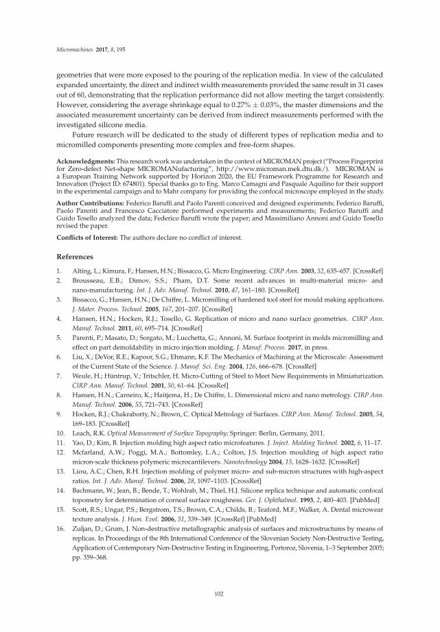
Micromachines 2017, 8, 195
geometries that were more exposed to the pouring of the replication media. In view of the calculatedexpanded uncertainty, the direct and indirect width measurements provided the same result in 31 casesout of 60, demonstrating that the replication performance did not allow meeting the target consistently.However, considering the average shrinkage equal to 0.27% ± 0.03%, the master dimensions and theassociated measurement uncertainty can be derived from indirect measurements performed with theinvestigated silicone media.
Future research will be dedicated to the study of different types of replication media and tomicromilled components presenting more complex and free-form shapes.
Acknowledgments: This research work was undertaken in the context of MICROMAN project (“Process Fingerprintfor Zero-defect Net-shape MICROMANufacturing”, http://www.microman.mek.dtu.dk/). MICROMAN isa European Training Network supported by Horizon 2020, the EU Framework Programme for Research andInnovation (Project ID: 674801). Special thanks go to Eng. Marco Camagni and Pasquale Aquilino for their supportin the experimental campaign and to Mahr company for providing the confocal microscope employed in the study.
Author Contributions: Federico Baruffi and Paolo Parenti conceived and designed experiments; Federico Baruffi,Paolo Parenti and Francesco Cacciatore performed experiments and measurements; Federico Baruffi andGuido Tosello analyzed the data; Federico Baruffi wrote the paper; and Massimiliano Annoni and Guido Tosellorevised the paper.
Conflicts of Interest: The authors declare no conflict of interest.
References
1. Alting, L.; Kimura, F.; Hansen, H.N.; Bissacco, G. Micro Engineering. CIRP Ann. 2003, 52, 635–657. [CrossRef]
2. Brousseau, E.B.; Dimov, S.S.; Pham, D.T. Some recent advances in multi-material micro- and
nano-manufacturing. Int. J. Adv. Manuf. Technol. 2010, 47, 161–180. [CrossRef]
3. Bissacco, G.; Hansen, H.N.; De Chiffre, L. Micromilling of hardened tool steel for mould making applications.
J. Mater. Process. Technol. 2005, 167, 201–207. [CrossRef]
4. Hansen, H.N.; Hocken, R.J.; Tosello, G. Replication of micro and nano surface geometries. CIRP Ann.
Manuf. Technol. 2011, 60, 695–714. [CrossRef]
5. Parenti, P.; Masato, D.; Sorgato, M.; Lucchetta, G.; Annoni, M. Surface footprint in molds micromilling and
effect on part demoldability in micro injection molding. J. Manuf. Process. 2017, in press.
6. Liu, X.; DeVor, R.E.; Kapoor, S.G.; Ehmann, K.F. The Mechanics of Machining at the Microscale: Assessment
of the Current State of the Science. J. Manuf. Sci. Eng. 2004, 126, 666–678. [CrossRef]
7. Weule, H.; Hüntrup, V.; Tritschler, H. Micro-Cutting of Steel to Meet New Requirements in Miniaturization.
CIRP Ann. Manuf. Technol. 2001, 50, 61–64. [CrossRef]
8. Hansen, H.N.; Carneiro, K.; Haitjema, H.; De Chiffre, L. Dimensional micro and nano metrology. CIRP Ann.
Manuf. Technol. 2006, 55, 721–743. [CrossRef]
9. Hocken, R.J.; Chakraborty, N.; Brown, C. Optical Metrology of Surfaces. CIRP Ann. Manuf. Technol. 2005, 54,
169–183. [CrossRef]
10. Leach, R.K. Optical Measurement of Surface Topography; Springer: Berlin, Germany, 2011.
11. Yao, D.; Kim, B. Injection molding high aspect ratio microfeatures. J. Inject. Molding Technol. 2002, 6, 11–17.
12. Mcfarland, A.W.; Poggi, M.A.; Bottomley, L.A.; Colton, J.S. Injection moulding of high aspect ratio
micron-scale thickness polymeric microcantilevers. Nanotechnology 2004, 15, 1628–1632. [CrossRef]
13. Liou, A.C.; Chen, R.H. Injection molding of polymer micro- and sub-micron structures with high-aspect
ratios. Int. J. Adv. Manuf. Technol. 2006, 28, 1097–1103. [CrossRef]
14. Bachmann, W.; Jean, B.; Bende, T.; Wohlrab, M.; Thiel, H.J. Silicone replica technique and automatic confocal
topometry for determination of corneal surface roughness. Ger. J. Ophthalmol. 1993, 2, 400–403. [PubMed]
15. Scott, R.S.; Ungar, P.S.; Bergstrom, T.S.; Brown, C.A.; Childs, B.; Teaford, M.F.; Walker, A. Dental microwear
texture analysis. J. Hum. Evol. 2006, 51, 339–349. [CrossRef] [PubMed]
16. Zuljan, D.; Grum, J. Non-destructive metallographic analysis of surfaces and microstructures by means of
replicas. In Proceedings of the 8th International Conference of the Slovenian Society Non-Destructive Testing,
Application of Contemporary Non-Destructive Testing in Engineering, Portoroz, Slovenia, 1–3 September 2005;
pp. 359–368.
102

Micromachines 2017, 8, 195
17. Jordon, J.B.; Bernard, J.D.; Newman, J.C. Quantifying microstructurally small fatigue crack growth in
an aluminum alloy using a silicon-rubber replica method. Int. J. Fatigue 2012, 36, 206–210. [CrossRef]
18. AccuTrans 2012 AccuTrans Brochure. Available online: http://www.accutrans.info/fileadmin/dam/DATEN/
AccuTrans/downloads/others/30000992_11--12_IFU_AccuTrans_AM_01.pdf (accessed on 15 February 2017).
19. Struers 2008 RepliSet Brochure. Available online: http://www.struers.com/en-GB/Products/Materialographic-
analysis/Materialographic-analysis-equipment/Replication-system (accessed on 15 February 2017).
20. Tosello, G.; Hansen, H.N.; Gasparin, S.; Albajez, J.A.; Esmoris, J.I. Surface wear of TiN coated nickel tool
during the injection moulding of polymer micro Fresnel lenses. CIRP Ann. Manuf. Technol. 2012, 61, 535–538.
[CrossRef]
21. Madsen, M.H.; Feidenhans’l, N.A.; Hansen, P.-E.; Garnæs, J.; Dirscherl, K. Accounting for PDMS shrinkage
when replicating structures. J. Micromech. Microeng. 2014, 24, 127002. [CrossRef]
22. Goodall, R.H.; Darras, L.P.; Purnell, M.A. Accuracy and precision of silicon based impression media for
quantitative areal texture analysis. Sci. Rep. 2015, 5, 10800. [CrossRef] [PubMed]
23. Gasparin, S.; Hansen, H.N.; Tosello, G. Traceable surface characterization using replica moulding technology.
In Proceedings of the 13th International Conference on Metrology Properties of English Surfaces, Kgs,
Lyngby, Denmark, 12–15 April 2011; pp. 306–315.
24. Jinsheng, W.; Dajian, Z.; Yadong, G. A Micromilling Experimental Study on AISI 4340 Steel. Key Eng. Mater.
2009, 408, 335–338.
25. Kiswanto, G.; Zariatin, D.L.; Ko, T.J. The effect of spindle speed, feed-rate and machining time to the surface
roughness and burr formation of Aluminum Alloy 1100 in micro-milling operation. J. Manuf. Process.
2014, 16, 435–450. [CrossRef]
26. Wang, J.; Gong, Y.; Shi, J.; Abba, G. Surface Roughness Prediction in Micromilling using Neural Networks
and Taguchi’s Design of Experiments. In Proceedings of the IEEE International Conference on Industrial
Engineering and Engineering Managament (IEEM), Gippsland, Auatralia, 8–11 December 2009; pp. 1–6.
27. Cardoso, P.; Davim, J.P. Optimization of Surface Roughness in Micromilling. Mater. Manuf. Process. 2010, 25,
1115–1119. [CrossRef]
28. Liu, X.; DeVor, R.E.; Kapoor, S.G. Model-Based Analysis of the Surface Generation in Microendmilling—Part I:
Model Development. J. Manuf. Sci. Eng. 2007, 129, 453–460. [CrossRef]
29. Abdelrahman Elkaseer, A.M.; Dimov, S.S.; Popov, K.B.; Negm, M.; Minev, R. Modeling the Material
Microstructure Effects on the Surface Generation Process in Microendmilling of Dual-Phase Materials.
J. Manuf. Sci. Eng. 2012, 134, 44501. [CrossRef]
30. Schwenke, H.; Neuschaefer-Rube, U.; Pfeifer, T.; Kunzmann, H. Optical Methods for Dimensional Metrology
in Production Engineering. CIRP Ann. Manuf. Technol. 2002, 51, 685–699. [CrossRef]
31. Marinello, F.; Bariani, P.; De Chiffre, L.; Hansen, H.N. Development and analysis of a software tool for
stitching three-dimensional surface topography data sets. Meas. Sci. Technol. 2007, 18, 1404–1412. [CrossRef]
32. MountainsMap®, Digital Surf. Available online: http://www.digitalsurf.fr/en/mntkey.html (accessed on
15 February 2017).
33. ISO. IOS 25178-2: Geometrical Product Specifications (GPS)—Surface Texture: Areal—Part 2: Terms, Definitions
and Surface Texture Parameters; IOS: Geneva, Switzerland, 2012.
34. Joint Committee for Guides in Metrology (JCGM). Evaluation of Measurement Data: Guide to the Expression of
Uncertainty in Measurement; JCGM: Paris, France, 2008.
35. ISO. IOS 15530-3: Geometrical Product Specifications (GPS)—Coordinate Measuring Machines (CMM): Technique
for Determining the Uncertainty of Measurement; IOS: Geneva, Switzerland, 2011.
36. Haitjema, H. Uncertainty in measurement of surface topography. Surf. Topogr. Metrol. Prop. 2015, 3, 35004.
[CrossRef]
37. Tosello, G.; Haitjema, H.; Leach, R.K.; Quagliotti, D.; Gasparin, S.; Hansen, H.N. An international comparison
of surface texture parameters quantification on polymer artefacts using optical instruments. CIRP Ann.
Manuf. Technol. 2016, 65, 529–532. [CrossRef]
© 2017 by the authors. Licensee MDPI, Basel, Switzerland. This article is an open access
article distributed under the terms and conditions of the Creative Commons Attribution
(CC BY) license (http://creativecommons.org/licenses/by/4.0/).
103
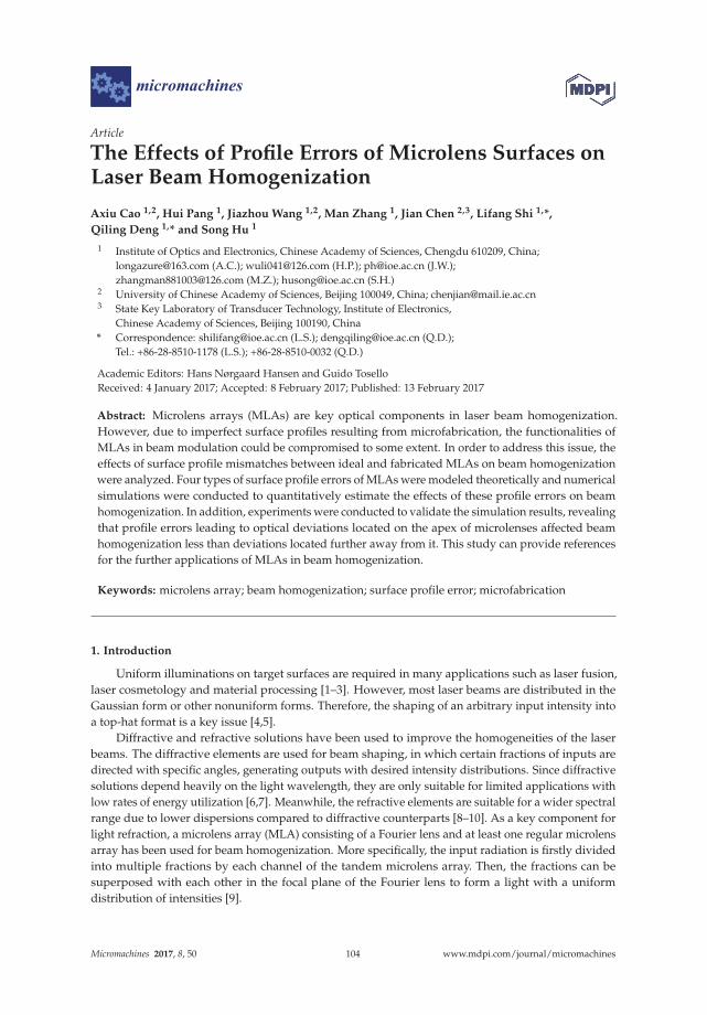
micromachines
Article
The Effects of Profile Errors of Microlens Surfaces onLaser Beam Homogenization
Axiu Cao 1,2, Hui Pang 1, Jiazhou Wang 1,2, Man Zhang 1, Jian Chen 2,3, Lifang Shi 1,*,
Qiling Deng 1,* and Song Hu 1
1 Institute of Optics and Electronics, Chinese Academy of Sciences, Chengdu 610209, China;[email protected] (A.C.); [email protected] (H.P.); [email protected] (J.W.);[email protected] (M.Z.); [email protected] (S.H.)
2 University of Chinese Academy of Sciences, Beijing 100049, China; [email protected] State Key Laboratory of Transducer Technology, Institute of Electronics,
Chinese Academy of Sciences, Beijing 100190, China* Correspondence: [email protected] (L.S.); [email protected] (Q.D.);
Tel.: +86-28-8510-1178 (L.S.); +86-28-8510-0032 (Q.D.)
Academic Editors: Hans Nørgaard Hansen and Guido ToselloReceived: 4 January 2017; Accepted: 8 February 2017; Published: 13 February 2017
Abstract: Microlens arrays (MLAs) are key optical components in laser beam homogenization.However, due to imperfect surface profiles resulting from microfabrication, the functionalities ofMLAs in beam modulation could be compromised to some extent. In order to address this issue, theeffects of surface profile mismatches between ideal and fabricated MLAs on beam homogenizationwere analyzed. Four types of surface profile errors of MLAs were modeled theoretically and numericalsimulations were conducted to quantitatively estimate the effects of these profile errors on beamhomogenization. In addition, experiments were conducted to validate the simulation results, revealingthat profile errors leading to optical deviations located on the apex of microlenses affected beamhomogenization less than deviations located further away from it. This study can provide referencesfor the further applications of MLAs in beam homogenization.
Keywords: microlens array; beam homogenization; surface profile error; microfabrication
1. Introduction
Uniform illuminations on target surfaces are required in many applications such as laser fusion,laser cosmetology and material processing [1–3]. However, most laser beams are distributed in theGaussian form or other nonuniform forms. Therefore, the shaping of an arbitrary input intensity intoa top-hat format is a key issue [4,5].
Diffractive and refractive solutions have been used to improve the homogeneities of the laserbeams. The diffractive elements are used for beam shaping, in which certain fractions of inputs aredirected with specific angles, generating outputs with desired intensity distributions. Since diffractivesolutions depend heavily on the light wavelength, they are only suitable for limited applications withlow rates of energy utilization [6,7]. Meanwhile, the refractive elements are suitable for a wider spectralrange due to lower dispersions compared to diffractive counterparts [8–10]. As a key component forlight refraction, a microlens array (MLA) consisting of a Fourier lens and at least one regular microlensarray has been used for beam homogenization. More specifically, the input radiation is firstly dividedinto multiple fractions by each channel of the tandem microlens array. Then, the fractions can besuperposed with each other in the focal plane of the Fourier lens to form a light with a uniformdistribution of intensities [9].
Micromachines 2017, 8, 50 104 www.mdpi.com/journal/micromachines
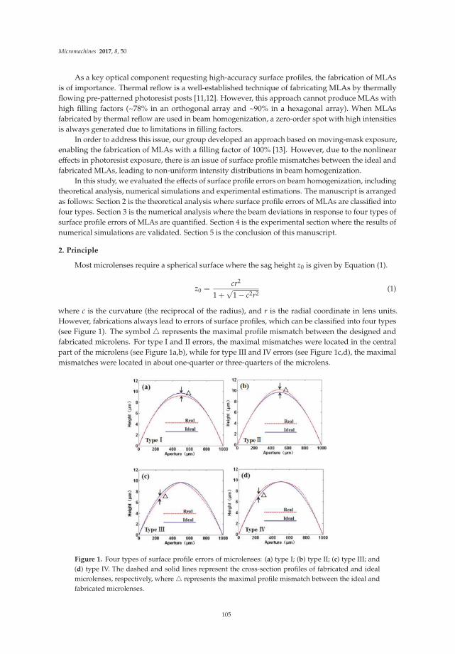
Micromachines 2017, 8, 50
As a key optical component requesting high-accuracy surface profiles, the fabrication of MLAsis of importance. Thermal reflow is a well-established technique of fabricating MLAs by thermallyflowing pre-patterned photoresist posts [11,12]. However, this approach cannot produce MLAs withhigh filling factors (~78% in an orthogonal array and ~90% in a hexagonal array). When MLAsfabricated by thermal reflow are used in beam homogenization, a zero-order spot with high intensitiesis always generated due to limitations in filling factors.
In order to address this issue, our group developed an approach based on moving-mask exposure,enabling the fabrication of MLAs with a filling factor of 100% [13]. However, due to the nonlineareffects in photoresist exposure, there is an issue of surface profile mismatches between the ideal andfabricated MLAs, leading to non-uniform intensity distributions in beam homogenization.
In this study, we evaluated the effects of surface profile errors on beam homogenization, includingtheoretical analysis, numerical simulations and experimental estimations. The manuscript is arrangedas follows: Section 2 is the theoretical analysis where surface profile errors of MLAs are classified intofour types. Section 3 is the numerical analysis where the beam deviations in response to four types ofsurface profile errors of MLAs are quantified. Section 4 is the experimental section where the results ofnumerical simulations are validated. Section 5 is the conclusion of this manuscript.
2. Principle
Most microlenses require a spherical surface where the sag height z0 is given by Equation (1).
z0 =cr2
1 +√
1 − c2r2(1)
where c is the curvature (the reciprocal of the radius), and r is the radial coordinate in lens units.However, fabrications always lead to errors of surface profiles, which can be classified into four types(see Figure 1). The symbol � represents the maximal profile mismatch between the designed andfabricated microlens. For type I and II errors, the maximal mismatches were located in the centralpart of the microlens (see Figure 1a,b), while for type III and IV errors (see Figure 1c,d), the maximalmismatches were located in about one-quarter or three-quarters of the microlens.
Figure 1. Four types of surface profile errors of microlenses: (a) type I; (b) type II; (c) type III; and(d) type IV. The dashed and solid lines represent the cross-section profiles of fabricated and idealmicrolenses, respectively, where � represents the maximal profile mismatch between the ideal andfabricated microlenses.
105
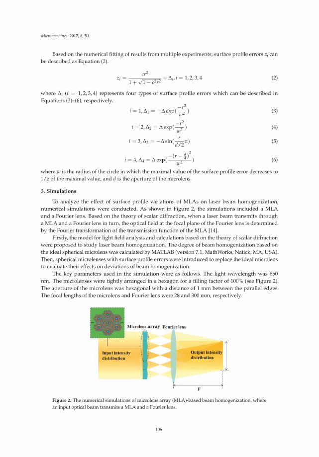
Micromachines 2017, 8, 50
Based on the numerical fitting of results from multiple experiments, surface profile errors zi canbe described as Equation (2).
zi =cr2
1 +√
1 − c2r2+ ∆i, i = 1, 2, 3, 4 (2)
where ∆i (i = 1, 2, 3, 4) represents four types of surface profile errors which can be described inEquations (3)–(6), respectively.
i = 1, ∆1 = −∆ exp(−r2
w2 ) (3)
i = 2, ∆2 = ∆ exp(−r2
w2 ) (4)
i = 3, ∆3 = −∆ sin(r
d/2π) (5)
i = 4, ∆4 = ∆ exp(−(r − d
4 )2
w2 ) (6)
where w is the radius of the circle in which the maximal value of the surface profile error decreases to1/e of the maximal value, and d is the aperture of the microlens.
3. Simulations
To analyze the effect of surface profile variations of MLAs on laser beam homogenization,numerical simulations were conducted. As shown in Figure 2, the simulations included a MLAand a Fourier lens. Based on the theory of scalar diffraction, when a laser beam transmits througha MLA and a Fourier lens in turn, the optical field at the focal plane of the Fourier lens is determinedby the Fourier transformation of the transmission function of the MLA [14].
Firstly, the model for light field analysis and calculations based on the theory of scalar diffractionwere proposed to study laser beam homogenization. The degree of beam homogenization based onthe ideal spherical microlens was calculated by MATLAB (version 7.1, MathWorks, Natick, MA, USA).Then, spherical microlenses with surface profile errors were introduced to replace the ideal microlensto evaluate their effects on deviations of beam homogenization.
The key parameters used in the simulation were as follows. The light wavelength was 650nm. The microlenses were tightly arranged in a hexagon for a filling factor of 100% (see Figure 2).The aperture of the microlens was hexagonal with a distance of 1 mm between the parallel edges.The focal lengths of the microlens and Fourier lens were 28 and 300 mm, respectively.
Figure 2. The numerical simulations of microlens array (MLA)-based beam homogenization, wherean input optical beam transmits a MLA and a Fourier lens.
106

Micromachines 2017, 8, 50
When the maximal surface profile errors were 0, 0.3, 0.5, 0.7 or 0.9 µm (the value of � in micronshas been quoted as a percentage of the microlens height), the corresponding deviation of beamhomogenization was obtained, respectively (see Figure 3). With the increase of the surface profileerrors, the side effects on the intensity distribution of the beam outputs became more and more obvious,indicated by a spot with non-uniform intensities. For type I and type IV errors, the output light wasshown to gradually converge to the center along with the increasing values of the surface profile error.On the contrary, for type II and type III errors, the output light was shown to gradually deviate fromthe center along with the increasing values of the surface profile error. When the values of the surfaceprofile errors were identical for these four types of situations, type III and IV errors exerted moreinfluence than type I and II errors (see Figure 3c1–c4).
Figure 3. Numerical simulations of images after beam homogenization by passing MLAs withfour types of surface profile errors. The maximal surface profile errors were 0 µm (0%) for (a1–a4);0.3 µm (3.6%) for (b1–b4); 0.5 µm (5.11%) for (c1–c4); 0.7 µm (7.15%) for (d1–d4); and 0.9 µm (9.19%)for (e1–e4), respectively.
In order to quantitatively compare the influences of four types of surface profile errors on beamhomogeneity, a key parameter η was defined as shown in Equation (7).
η =Imax − Imin
Imax + Imin× 100% (7)
where Imax and Imin represent the maximal and minimal intensities within the output spot, neglectingthe effect of the periodic interference pattern.
The non-uniformities of the surface profile errors within 1 µm were calculated in simulations,as shown in Figure 4. With an increase in the maximal surface profile error �, non-uniformity η wasalso shown to increase. Again, errors of type III and IV demonstrated more significant effects on beamhomogeneity than the other two types of errors. More specifically, a sudden increase in the slope of thenon-uniformity metric of 0.4 was observed for type III and IV errors and a further increase of errorsled to rapid increases of non-uniformities.
107
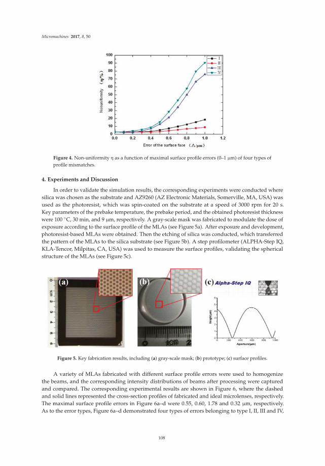
Micromachines 2017, 8, 50
Figure 4. Non-uniformity η as a function of maximal surface profile errors (0–1 µm) of four types ofprofile mismatches.
4. Experiments and Discussion
In order to validate the simulation results, the corresponding experiments were conducted wheresilica was chosen as the substrate and AZ9260 (AZ Electronic Materials, Somerville, MA, USA) wasused as the photoresist, which was spin-coated on the substrate at a speed of 3000 rpm for 20 s.Key parameters of the prebake temperature, the prebake period, and the obtained photoresist thicknesswere 100 ◦C, 30 min, and 9 µm, respectively. A gray-scale mask was fabricated to modulate the dose ofexposure according to the surface profile of the MLAs (see Figure 5a). After exposure and development,photoresist-based MLAs were obtained. Then the etching of silica was conducted, which transferredthe pattern of the MLAs to the silica substrate (see Figure 5b). A step profilometer (ALPHA-Step IQ,KLA-Tencor, Milpitas, CA, USA) was used to measure the surface profiles, validating the sphericalstructure of the MLAs (see Figure 5c).
Figure 5. Key fabrication results, including (a) gray-scale mask; (b) prototype; (c) surface profiles.
A variety of MLAs fabricated with different surface profile errors were used to homogenizethe beams, and the corresponding intensity distributions of beams after processing were capturedand compared. The corresponding experimental results are shown in Figure 6, where the dashedand solid lines represented the cross-section profiles of fabricated and ideal microlenses, respectively.The maximal surface profile errors in Figure 6a–d were 0.55, 0.60, 1.78 and 0.32 µm, respectively.As to the error types, Figure 6a–d demonstrated four types of errors belonging to type I, II, III and IV,
108

Micromachines 2017, 8, 50
respectively. The theoretical boundary of the expected outer envelope of the irradiated region wasdrawn with lines in a white color on each image, as shown in Figure 6.
Figure 6. Experimental results of images processed by MLAs with different surface profile errors.The maximal errors were quantified as (a) � = 0.55 µm (type I); (b) � = 0.60 µm (type II); (c) � = 1.78 µm(type III); and (d) � = 0.32 µm (type IV).
This deviation of beam homogenization can be explained as follows. The input beam was firstlysegmented into several sub-beams by the microlens and then the sub-beams were overlapped witheach other through the Fourier lens, generating a uniform intensity distribution. The surface profileerrors of the fabricated microlenses led to the irregular distributions of sub-beams, resulting in theredistribution of the divergence angles. Therefore, the output intensity was no longer uniform, and wasaffected by the fidelities of the surface profiles of microlenses.
If the fabricated microlens showed a type I, surface profile error the curvature of the surfaceprofiles around the light axis at the central region of the microlens was shown to reduce. Therefore, therefractive angle of the light in the corresponding region decreased compared with the light in the sameregion of the ideal microlens. Since the scale of the light with smaller refractive angles increased, theintensity converged by the Fourier lens was significantly enhanced in the center of the output spot.On the contrary, if the fabricated microlens suffered from a type II surface profile error, the refractiveangle of the light in the corresponding region was shown to increase because of the increase of thecurvature of the surface profile. Therefore, the intensity was reduced in the center of the output spotbecause of the decreases in both light intensities and refractive angles.
In addition, when the fabricated microlens demonstrated a type III surface profile error, thecurvature of the surface profile firstly increased and then decreased along the direction from the centerto the edge of the microlens, compared with the ideal surface profiles. Then the amount of the lightwith smaller or bigger refractive angles decreased. Therefore, the intensity which should converge atthe center and edge of the output spot was translated to regions between the center and the boundaryareas. Thus, the intensities at the central and marginal regions were very weak. On the contrary, whenthe fabricated microlens showed a type IV surface profile error, the corresponding curvature of thesurface profile changed in the opposite direction. Therefore, the intensity which should converge inthe region between the central and the boundary areas of the output spot was modulated into theregions of the center and the edges.
109

Micromachines 2017, 8, 50
Overall, the type III and IV surface profile errors nearly changed the whole surface of the microlenswhile type I and II surface profile errors only affected one half of the microlens. Therefore, the typeIII and IV surface profile errors demonstrated more significant influences on beam homogenization.In order to realize beam homogenization, the surface profile errors have to be controlled withina certain range at which the side influences can be tolerated. Meanwhile, the type III and IV surfaceprofile errors should be avoided because of their significant side effects.
5. Conclusions
In conclusion, in this study, effects of surface profile mismatches between fabricated and idealMLAs on beam homogenization were compared and studied. Both numerical simulations andexperimental results quantitatively located the side effects of surface profile errors. These resultssuggest profile deviations located further away from the apex of the microlenses should be avoidedin the future fabrication of MLAs since they demonstrated more significant side effects in beamhomogenization in comparison to profile errors located on the apex of the microlenses. Hopefully, thisstudy can provide references for the future study of beam homogenization–leveraging microlens arrays.
Acknowledgments: This research was supported by the National Natural Science Foundation of China (NSFC)(Nos. 61505214, 61605211); the Applied Basic Research Programs of Department of Science and Technology ofSichuan Province (Nos. 2016JY0175, 2016RZ0067); the National Defense Foundation of China (No. CXJJ-16M116);the Youth Innovation Promotion Association, Chinese Academy of Sciences (CAS); the CAS “Light of West China”Program. The authors thank their colleagues for their discussions and suggestions to this research.
Author Contributions: Axiu Cao and Hui Pang conceived and designed the experiments; Jiazhou Wang andMan Zhang performed the experiments while Lifang Shi and Qiling Deng supervised the whole process; Axiu Caoanalyzed the data; Song Hu contributed reagents/materials/analysis tools; Axiu Cao and Jian Chen wrote andrevised the paper.
Conflicts of Interest: The authors declare no conflict of interest.
References
1. Lou, S.; Zhu, H.; Han, P. Laser beam homogenizing system design for photoluminescence. Appl. Opt. 2014,
53, 4637–4644. [CrossRef]
2. Kim, J.W.; Mackenzie, J.I.; Hayes, J.R.; Clarkson, W.A. High-power Er: YAG laser with quasi-top-hat output
beam. Opt. Lett. 2012, 37, 1463–1465. [CrossRef] [PubMed]
3. Yao, P.H.; Chen, C.H.; Chen, C.H. Low speckle laser illuminated projection system with a vibrating diffractive
beam shaper. Opt. Express 2012, 20, 16552–16566. [CrossRef]
4. Sinhoff, V.; Hambuecker, S.; Kleine, K.; Ruebenach, O.; Wessling, C. Micro-lens arrays for laser beam
homogenization and transformation. Proc. SPIE 2013, 8605, 860509.
5. Wippermann, F.; Zeitner, U.; Dannberg, P. Beam homogenizers based on chirped microlens arrays.
Opt. Express 2007, 15, 6218–6231. [CrossRef] [PubMed]
6. Deller, M. Laser Beam Shaping: Theory and Techniques; Dickey, F.M., Holswade, S.C., Eds.; CRC Press (Taylor and
Francis Group): Boca Raton, FL, USA, 2000.
7. Pepler, D.A.; Danson, C.N.; Ross, I.N.; Rivers, S.; Edwards, S. Binary-phase Fresnel zone plate arrays for
high-power laser beam smoothing. Proc. SPIE 1995, 2404, 258–265.
8. Zhou, A.F. UV excimer laser beam homogenization for micromachining applications. Opt. Photonics Lett.
2011, 4, 75–81. [CrossRef]
9. Deng, X.M.; Liang, X.B.; Chen, Z.Z.; Yu, W.Y.; Ma, R.Y. Uniform illumination of large targets using a lens
array. Appl. Opt. 1986, 25, 377–381. [CrossRef] [PubMed]
10. Kamon, K. Flye-Eye Lens Device and Lighting System Including Same. U.S. Patent No. 5,251,067, 5
October 1993.
11. Lin, C.P.; Yang, H.; Chao, C.K. Hexagonal microlens array modeling and fabrication using a thermal reflow
process. J. Micromech. Microeng. 2003, 13, 775–781. [CrossRef]
12. Mohammed, A.; Cherry, G.; Franck, C.; Stuart, V.S.; Rajdeep, S.R. Geometrical characterization techniques
for microlens made by thermal reflow of photoresist cylinder. Opt. Lasers Eng. 2008, 46, 711–720.
110

Micromachines 2017, 8, 50
13. Shi, L.F.; Du, C.L.; Dong, X.C.; Deng, Q.L.; Luo, X.G. Effective formation method for an aspherical microlens
array based on an aperiodic moving mask during exposure. Appl. Opt. 2007, 46, 8346–8350. [CrossRef]
[PubMed]
14. Cao, A.X.; Pang, H.; Wang, J.Z.; Zhang, M.; Shi, L.F.; Deng, Q.L. Center off-axis tandem microlens arrays for
beam homogenization. IEEE Photonics J. 2015, 7, 2400207. [CrossRef]
© 2017 by the authors. Licensee MDPI, Basel, Switzerland. This article is an open access
article distributed under the terms and conditions of the Creative Commons Attribution
(CC BY) license (http://creativecommons.org/licenses/by/4.0/).
111
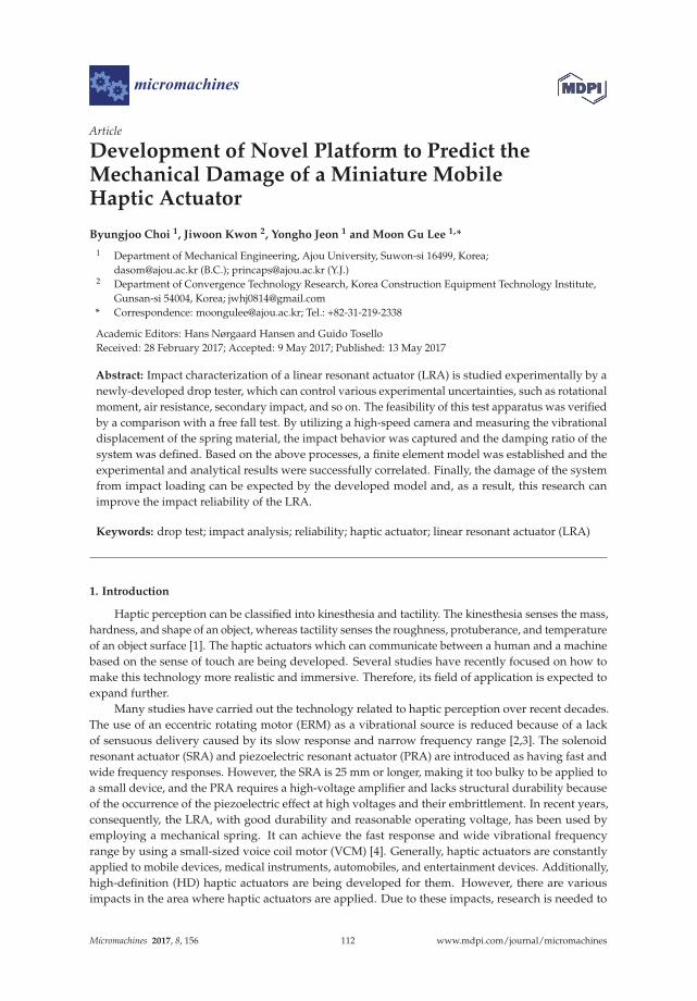
micromachines
Article
Development of Novel Platform to Predict theMechanical Damage of a Miniature MobileHaptic Actuator
Byungjoo Choi 1, Jiwoon Kwon 2, Yongho Jeon 1 and Moon Gu Lee 1,*
1 Department of Mechanical Engineering, Ajou University, Suwon-si 16499, Korea;[email protected] (B.C.); [email protected] (Y.J.)
2 Department of Convergence Technology Research, Korea Construction Equipment Technology Institute,Gunsan-si 54004, Korea; [email protected]
* Correspondence: [email protected]; Tel.: +82-31-219-2338
Academic Editors: Hans Nørgaard Hansen and Guido ToselloReceived: 28 February 2017; Accepted: 9 May 2017; Published: 13 May 2017
Abstract: Impact characterization of a linear resonant actuator (LRA) is studied experimentally by anewly-developed drop tester, which can control various experimental uncertainties, such as rotationalmoment, air resistance, secondary impact, and so on. The feasibility of this test apparatus was verifiedby a comparison with a free fall test. By utilizing a high-speed camera and measuring the vibrationaldisplacement of the spring material, the impact behavior was captured and the damping ratio of thesystem was defined. Based on the above processes, a finite element model was established and theexperimental and analytical results were successfully correlated. Finally, the damage of the systemfrom impact loading can be expected by the developed model and, as a result, this research canimprove the impact reliability of the LRA.
Keywords: drop test; impact analysis; reliability; haptic actuator; linear resonant actuator (LRA)
1. Introduction
Haptic perception can be classified into kinesthesia and tactility. The kinesthesia senses the mass,hardness, and shape of an object, whereas tactility senses the roughness, protuberance, and temperatureof an object surface [1]. The haptic actuators which can communicate between a human and a machinebased on the sense of touch are being developed. Several studies have recently focused on how tomake this technology more realistic and immersive. Therefore, its field of application is expected toexpand further.
Many studies have carried out the technology related to haptic perception over recent decades.The use of an eccentric rotating motor (ERM) as a vibrational source is reduced because of a lackof sensuous delivery caused by its slow response and narrow frequency range [2,3]. The solenoidresonant actuator (SRA) and piezoelectric resonant actuator (PRA) are introduced as having fast andwide frequency responses. However, the SRA is 25 mm or longer, making it too bulky to be applied toa small device, and the PRA requires a high-voltage amplifier and lacks structural durability becauseof the occurrence of the piezoelectric effect at high voltages and their embrittlement. In recent years,consequently, the LRA, with good durability and reasonable operating voltage, has been used byemploying a mechanical spring. It can achieve the fast response and wide vibrational frequencyrange by using a small-sized voice coil motor (VCM) [4]. Generally, haptic actuators are constantlyapplied to mobile devices, medical instruments, automobiles, and entertainment devices. Additionally,high-definition (HD) haptic actuators are being developed for them. However, there are variousimpacts in the area where haptic actuators are applied. Due to these impacts, research is needed to
Micromachines 2017, 8, 156 112 www.mdpi.com/journal/micromachines

Micromachines 2017, 8, 156
make this device reliable. Such efforts have been made in related industries, but there is a need tomake systematic forecasts because the existing ones are based on the trial and error method with thedesigner’s experience.
Figure 1 shows the structure of an LRA (iPhone 4s, vibration motor). A spring, magnet, and movingmass are fixed on the top of the housing, while the coil is attached at the bottom of the housing. When acurrent is applied to the coil, a Lorentz force is generated due to the electromagnetic interactionbetween the current of the coil and the magnetic field. This force results in haptic perception by thevibration of the magnet and moving mass attached to the spring [5]. The structural durability of eachcomponent is a crucial part in the delivery of consistent haptic perception and, therefore, the relatedindustry requires high reliability for this system. In the case of the impact durability test droppingfrom 1.8 m, from a human ear’s height, only a 10% malfunction rate for the haptic actuator mountedin a smartphone is allowed in the industry. In order to satisfy this criterion, many suppliers haveperformed several research activities, such as reliability testing and analytical work [6–12]. The droptest, which is one of the experimental methods, is the most accurate way to study the impact resistanceof a mobile device. However, experimental approaches cannot effectively characterize the impactbehavior of each component because of its small size and behavior under a high-rate regime. In orderto solve this issue, the finite element analysis was introduced in this study and this approach wasverified by a comparison with the experimental approach.
(a) (b)
Figure 1. Appearance and internal structure of a coin-type LRA: (a) appearance; and (b) cross-sectional view.
Among the components in the actuator, the spring is the most sensitive part under impactloading and the impact damage can change the natural frequency of the spring, causing a malfunction,like insufficient acceleration.
In this study, we developed the novel platform which can predict the mechanical damage forLRA under impact loading. To generate the impact loading, the specific drop tester was developedand the repeatability test was executed for checking the feasibility of the test apparatus. Additionally,the analytical model was established and appropriate material testing was performed for obtainingthe mechanical property simultaneously. As the relevance of the analytical model was proved by acorrelation with experimental results, we can finally successfully predict the mechanical damage ofthe LRA under impact loading with the developed analytical model. We can assure that the researchoutput explained in this article can play a significant role for damage analysis of various electricaldevices under impact loading.
2. Drop Tester
2.1. Drop Tester Configuration
In general, the falling motion of the mobile device shows several aspects by rotation moment,air resistance, secondary impact, and so on. Therefore, it is very difficult to analyze the mechanicalbehavior experimentally due to the experimental uncertainty caused by the falling motion. In order tocontrol the experimental uncertainty, a new drop tester was developed.
113

Micromachines 2017, 8, 156
The experimental setup was constructed as shown in Figure 2. The impact force sensor (200C50,PCB Piezotronics Inc., Depew, NY, USA) can measure the frequency band of 0.0003 Hz to 30 kHzand a maximum dynamic compression force of 222.4 kN [13]. It was mounted onto the bottom of thetest system. The measured signal was acquired and saved by a data acquisition system (LABVIEW,National Instruments, Austin, TX, USA). Additionally, the high-speed camera (FASCAM, APX-RS,Photron, Tokyo, Japan) was introduced for capturing the impact behavior visually and the image wascaptured at 512 × 512 resolution and 10,000 fps with an LED light.
(a) (b)
Figure 2. Drop tester configuration: (a) schematic diagram; and (b) experimental setup.
The test specimen was fixed with an auto-release gripper, which was operated by a pneumaticsystem, and the gripper was attached to the bushing. When the test begins, the bushing starts fallingdown through the guide shaft and then the gripper releases the specimen passing the proximity sensor.Finally, the test object impacts the force sensor mounted onto the bottom part of the impact tester.To reduce the experimental uncertainty, especially friction during the falling of the object, the bushingwas composed of monomer cast nylon and grease was applied onto the guide shaft.
2.2. Drop Tester Verification
The developed drop tester consists of several supplementary components for controlling theexperimental uncertainty and this supplementary component can distort the impact behavior.Therefore, the feasibility of this test apparatus must be verified in an appropriate manner. In thisstudy, we fulfilled the verification of this feasibility by a comparison with the free fall test. A slenderrod was used as a specimen and this rod was wrapped with silicone rubber to mitigate the vibration.Both the rod with and without the constraint were dropped from a height of 1.8 m. This height is asimulated value of the height of human ears. The drop from this height will result in a severe impacton the devices.
Despite the small allowable error in the peak force and period, as shown in Figure 3 and Table 1,the primary impact and subsequent oscillation for both tests was well matched and the agreementbetween the free and assisted tests suggests that the test results with the newly-developed testapparatus shows good repeatability.
114
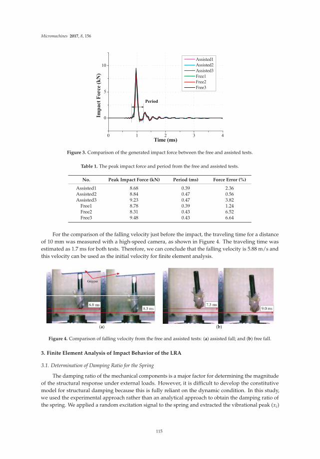
Micromachines 2017, 8, 156
0 1 2 3 4
0
5
10
Imp
act
Fo
rce
(kN
)
Time (ms)
Assisted1
Assisted2
Assisted3
Free1
Free2
Free3
Period
Figure 3. Comparison of the generated impact force between the free and assisted tests.
Table 1. The peak impact force and period from the free and assisted tests.
No. Peak Impact Force (kN) Period (ms) Force Error (%)
Assisted1 8.68 0.39 2.36Assisted2 8.84 0.47 0.56Assisted3 9.23 0.47 3.82
Free1 8.78 0.39 1.24Free2 8.31 0.43 6.52Free3 9.48 0.43 6.64
For the comparison of the falling velocity just before the impact, the traveling time for a distanceof 10 mm was measured with a high-speed camera, as shown in Figure 4. The traveling time wasestimated as 1.7 ms for both tests. Therefore, we can conclude that the falling velocity is 5.88 m/s andthis velocity can be used as the initial velocity for finite element analysis.
(a) (b)
Figure 4. Comparison of falling velocity from the free and assisted tests: (a) assisted fall; and (b) free fall.
3. Finite Element Analysis of Impact Behavior of the LRA
3.1. Determination of Damping Ratio for the Spring
The damping ratio of the mechanical components is a major factor for determining the magnitudeof the structural response under external loads. However, it is difficult to develop the constitutivemodel for structural damping because this is fully reliant on the dynamic condition. In this study,we used the experimental approach rather than an analytical approach to obtain the damping ratio ofthe spring. We applied a random excitation signal to the spring and extracted the vibrational peak (xi)
115
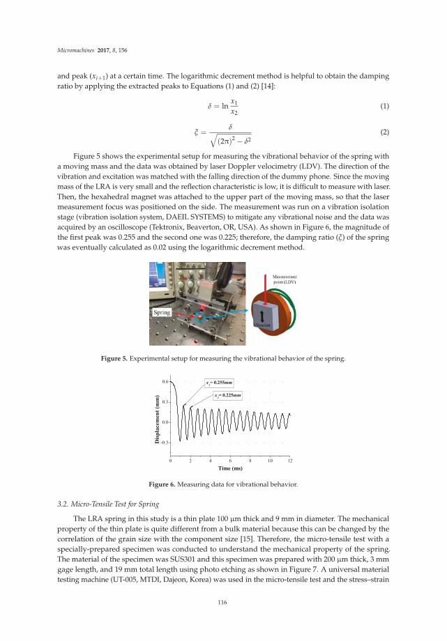
Micromachines 2017, 8, 156
and peak (xi+1) at a certain time. The logarithmic decrement method is helpful to obtain the dampingratio by applying the extracted peaks to Equations (1) and (2) [14]:
δ = lnx1
x2(1)
ξ =δ
√
(2π)2− δ2
(2)
Figure 5 shows the experimental setup for measuring the vibrational behavior of the spring witha moving mass and the data was obtained by laser Doppler velocimetry (LDV). The direction of thevibration and excitation was matched with the falling direction of the dummy phone. Since the movingmass of the LRA is very small and the reflection characteristic is low, it is difficult to measure with laser.Then, the hexahedral magnet was attached to the upper part of the moving mass, so that the lasermeasurement focus was positioned on the side. The measurement was run on a vibration isolationstage (vibration isolation system, DAEIL SYSTEMS) to mitigate any vibrational noise and the data wasacquired by an oscilloscope (Tektronix, Beaverton, OR, USA). As shown in Figure 6, the magnitude ofthe first peak was 0.255 and the second one was 0.225; therefore, the damping ratio (ξ) of the springwas eventually calculated as 0.02 using the logarithmic decrement method.
Figure 5. Experimental setup for measuring the vibrational behavior of the spring.
0 2 4 6 8 10 12
-0.3
0.0
0.3
0.6
x2= 0.225mm
Dis
pla
cem
en
t (m
m)
Time (ms)
x1= 0.255mm
Figure 6. Measuring data for vibrational behavior.
3.2. Micro-Tensile Test for Spring
The LRA spring in this study is a thin plate 100 µm thick and 9 mm in diameter. The mechanicalproperty of the thin plate is quite different from a bulk material because this can be changed by thecorrelation of the grain size with the component size [15]. Therefore, the micro-tensile test with aspecially-prepared specimen was conducted to understand the mechanical property of the spring.The material of the specimen was SUS301 and this specimen was prepared with 200 µm thick, 3 mmgage length, and 19 mm total length using photo etching as shown in Figure 7. A universal materialtesting machine (UT-005, MTDI, Dajeon, Korea) was used in the micro-tensile test and the stress–strain
116

Micromachines 2017, 8, 156
curve of the SUS301 is shown in Figure 8. Even though the ultimate tensile strength (UTS) of SUS301 isknown to be 1300 MPa [16], the UTS in this micro-tensile test was measured as 1510 MPa because ofthe size effect.
Figure 7. LRA spring test specimen.
0 2 4 6 8 100
400
800
1200
1600
Str
ess
(MP
a)
Strain (%)
Figure 8. Stress–strain curve of SUS301 obtained by the micro-tensile test.
3.3. Experimental Verification of Analytical Model
To mimic the cellular phone, the appropriate dummy phone was prepared and the finite element(FE) model was also generated for this physical model, as shown in Figure 9. The dummy phone wascomposed of an aluminum panel and the LRA was attached to the center of the panel. In general,the LRA is covered with a metal housing. This makes it difficult to measure the vibration of the movingmass. Therefore, the LRA housing was removed to observe the moving mass movement during theimpact moment. Additionally, this aluminum panel was covered by a transparent plate made ofpolycarbonate. This transparency allows the capturing of the behavior of the LRA by a high-speedcamera. The hexa and tetra element was applied as the FE model element and a fine mesh with a 60 µmelement size was applied in the spring and moving mass, which was our main interest. The impactthat a haptic actuator dropped from the 1.8 m ear’s height to the floor is a significant problem. In thiscase, a falling velocity was applied as 5.88 m/s, which was measured from the drop test just beforecollision, and gravitational acceleration was defined as 9.81 m/s2. Futhermore, the friction coefficientwas applied as 0.61 for static and 0.47 for kinetic, repectively.
(a) (b)
Figure 9. Physical and FE model of dummy phone with LRA: (a) dummy phone as a test specimen;and (b) finite element analysis.
117
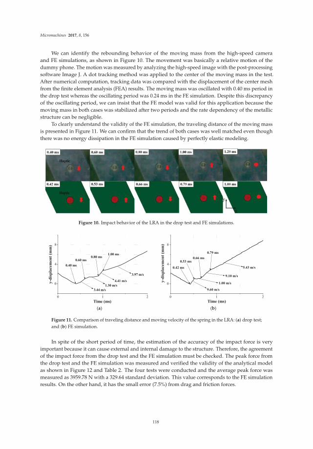
Micromachines 2017, 8, 156
We can identify the rebounding behavior of the moving mass from the high-speed cameraand FE simulations, as shown in Figure 10. The movement was basically a relative motion of thedummy phone. The motion was measured by analyzing the high-speed image with the post-processingsoftware Image J. A dot tracking method was applied to the center of the moving mass in the test.After numerical computation, tracking data was compared with the displacement of the center meshfrom the finite element analysis (FEA) results. The moving mass was oscillated with 0.40 ms period inthe drop test whereas the oscillating period was 0.24 ms in the FE simulation. Despite this discrepancyof the oscillating period, we can insist that the FE model was valid for this application because themoving mass in both cases was stabilized after two periods and the rate dependency of the metallicstructure can be negligible.
To clearly understand the validity of the FE simulation, the traveling distance of the moving massis presented in Figure 11. We can confirm that the trend of both cases was well matched even thoughthere was no energy dissipation in the FE simulation caused by perfectly elastic modeling.
Figure 10. Impact behavior of the LRA in the drop test and FE simulations.
(a) (b)
0 1 2
0
4
8
3.97 m/s
4.41 m/s
1.30 m/s
0.60 ms
1.00 ms0.80 ms
3.44 m/s
y-d
isp
lacem
en
t (m
m)
Time (ms)
0.40 ms
0 1 2
0
4
8
5.43 m/s
9.10 m/s
1.00 m/s
9.60 m/s
0.79 ms
0.66 ms0.53 ms
0.42 ms
y-d
isp
lace
men
t (m
m)
Time (ms)
Figure 11. Comparison of traveling distance and moving velocity of the spring in the LRA: (a) drop test;and (b) FE simulation.
In spite of the short period of time, the estimation of the accuracy of the impact force is veryimportant because it can cause external and internal damage to the structure. Therefore, the agreementof the impact force from the drop test and the FE simulation must be checked. The peak force fromthe drop test and the FE simulation was measured and verified the validity of the analytical modelas shown in Figure 12 and Table 2. The four tests were conducted and the average peak force wasmeasured as 3959.78 N with a 329.64 standard deviation. This value corresponds to the FE simulationresults. On the other hand, it has the small error (7.5%) from drag and friction forces.
118
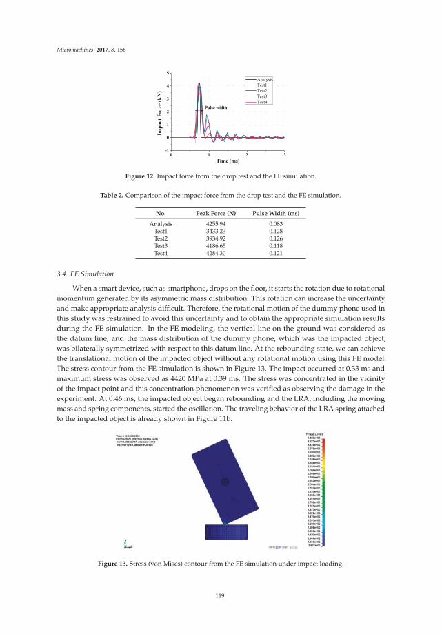
Micromachines 2017, 8, 156
0 1 2 3-1
0
1
2
3
4
5
Pulse width
Imp
act
Fo
rce
(kN
)Time (ms)
Analysis
Test1
Test2
Test3
Test4
Figure 12. Impact force from the drop test and the FE simulation.
Table 2. Comparison of the impact force from the drop test and the FE simulation.
No. Peak Force (N) Pulse Width (ms)
Analysis 4255.94 0.083Test1 3433.23 0.128Test2 3934.92 0.126Test3 4186.65 0.118Test4 4284.30 0.121
3.4. FE Simulation
When a smart device, such as smartphone, drops on the floor, it starts the rotation due to rotationalmomentum generated by its asymmetric mass distribution. This rotation can increase the uncertaintyand make appropriate analysis difficult. Therefore, the rotational motion of the dummy phone used inthis study was restrained to avoid this uncertainty and to obtain the appropriate simulation resultsduring the FE simulation. In the FE modeling, the vertical line on the ground was considered asthe datum line, and the mass distribution of the dummy phone, which was the impacted object,was bilaterally symmetrized with respect to this datum line. At the rebounding state, we can achievethe translational motion of the impacted object without any rotational motion using this FE model.The stress contour from the FE simulation is shown in Figure 13. The impact occurred at 0.33 ms andmaximum stress was observed as 4420 MPa at 0.39 ms. The stress was concentrated in the vicinityof the impact point and this concentration phenomenon was verified as observing the damage in theexperiment. At 0.46 ms, the impacted object began rebounding and the LRA, including the movingmass and spring components, started the oscillation. The traveling behavior of the LRA spring attachedto the impacted object is already shown in Figure 11b.
Figure 13. Stress (von Mises) contour from the FE simulation under impact loading.
119
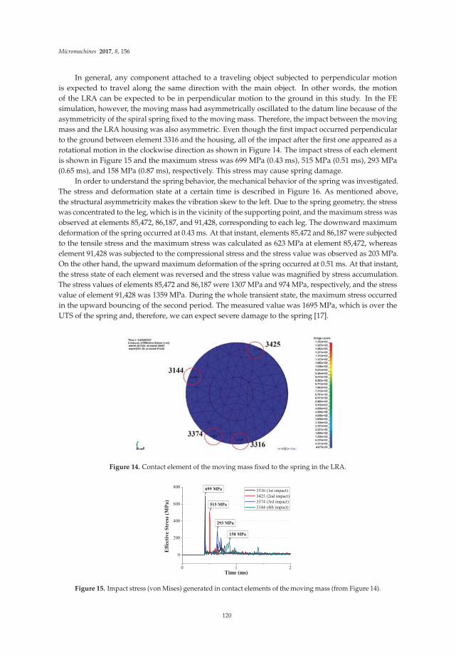
Micromachines 2017, 8, 156
In general, any component attached to a traveling object subjected to perpendicular motionis expected to travel along the same direction with the main object. In other words, the motionof the LRA can be expected to be in perpendicular motion to the ground in this study. In the FEsimulation, however, the moving mass had asymmetrically oscillated to the datum line because of theasymmetricity of the spiral spring fixed to the moving mass. Therefore, the impact between the movingmass and the LRA housing was also asymmetric. Even though the first impact occurred perpendicularto the ground between element 3316 and the housing, all of the impact after the first one appeared as arotational motion in the clockwise direction as shown in Figure 14. The impact stress of each elementis shown in Figure 15 and the maximum stress was 699 MPa (0.43 ms), 515 MPa (0.51 ms), 293 MPa(0.65 ms), and 158 MPa (0.87 ms), respectively. This stress may cause spring damage.
In order to understand the spring behavior, the mechanical behavior of the spring was investigated.The stress and deformation state at a certain time is described in Figure 16. As mentioned above,the structural asymmetricity makes the vibration skew to the left. Due to the spring geometry, the stresswas concentrated to the leg, which is in the vicinity of the supporting point, and the maximum stress wasobserved at elements 85,472, 86,187, and 91,428, corresponding to each leg. The downward maximumdeformation of the spring occurred at 0.43 ms. At that instant, elements 85,472 and 86,187 were subjectedto the tensile stress and the maximum stress was calculated as 623 MPa at element 85,472, whereaselement 91,428 was subjected to the compressional stress and the stress value was observed as 203 MPa.On the other hand, the upward maximum deformation of the spring occurred at 0.51 ms. At that instant,the stress state of each element was reversed and the stress value was magnified by stress accumulation.The stress values of elements 85,472 and 86,187 were 1307 MPa and 974 MPa, respectively, and the stressvalue of element 91,428 was 1359 MPa. During the whole transient state, the maximum stress occurredin the upward bouncing of the second period. The measured value was 1695 MPa, which is over theUTS of the spring and, therefore, we can expect severe damage to the spring [17].
Figure 14. Contact element of the moving mass fixed to the spring in the LRA.
0 1 2
0
200
400
600
800
158 MPa
293 MPa
515 MPa
Eff
ecti
ve
Str
ess
(MP
a)
Time (ms)
3316 (1st impact)
3425 (2nd impact)
3374 (3rd impact)
3144 (4th impact)
699 MPa
Figure 15. Impact stress (von Mises) generated in contact elements of the moving mass (from Figure 14).
120
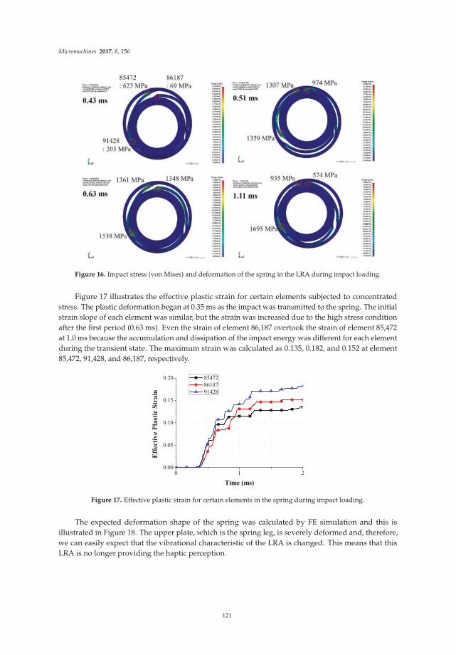
Micromachines 2017, 8, 156
Figure 16. Impact stress (von Mises) and deformation of the spring in the LRA during impact loading.
Figure 17 illustrates the effective plastic strain for certain elements subjected to concentratedstress. The plastic deformation began at 0.35 ms as the impact was transmitted to the spring. The initialstrain slope of each element was similar, but the strain was increased due to the high stress conditionafter the first period (0.63 ms). Even the strain of element 86,187 overtook the strain of element 85,472at 1.0 ms because the accumulation and dissipation of the impact energy was different for each elementduring the transient state. The maximum strain was calculated as 0.135, 0.182, and 0.152 at element85,472, 91,428, and 86,187, respectively.
0 1 20.00
0.05
0.10
0.15
0.20
Eff
ect
ive
Pla
stic
Str
ain
Time (ms)
85472
86187
91428
Figure 17. Effective plastic strain for certain elements in the spring during impact loading.
The expected deformation shape of the spring was calculated by FE simulation and this isillustrated in Figure 18. The upper plate, which is the spring leg, is severely deformed and, therefore,we can easily expect that the vibrational characteristic of the LRA is changed. This means that thisLRA is no longer providing the haptic perception.
121

Micromachines 2017, 8, 156
Figure 18. Expected deformation shape (highlighted with red lines) of the spring after the impact.
4. Conclusions
We developed a novel platform which can predict the mechanical damage for an LRA underimpact loading by using drop test and FE analysis methods.
(1) For the analysis, a series of preparations were carried out. First, the drop tester was newly-developedfor experimental verification of the FE model. Its experimental verification satisfied the freefall conditions while assisting the drop with a test apparatus. Second, a micro-tensile test wasperformed to obtain the material properties considering the size effect of the thin LRA springs. Third,structural damping was modeled by measuring the vibration displacement of a spring with theexcitation signal.
(2) Based on the previous study, the impact FE modeling of a dummy phone including an LRAwas performed, and its experimental verification was carried out by comparison of the impactdeformation and force during the impact behavior. Despite the error in the impact force (7.5%)and pulse width (33%), the analytical model and experimental model were well correlated.Additionally, the impact rebound displacement is well matched.
(3) Consequently, the damage of the FE model was analyzed. The external impact and secondaryinternal impact of the LRA moving mass were concentrated on the LRA spring. Primary andsecondary impact generated a maximum impact stress of 1695 MPa. Further, effective strain atthe same position was evaluated as 0.182. The damaged shape of the spring was confirmed and avibration characteristic change was expected.
In conclusion, impact deformation and force were calculated through an experimentally-verifiedFE model. This process can redeem the durability study against impact which has been conducted bythe designer’s experience and trial-and-error. Finally, this research will be used extensively in impactanalysis of smart devices, automobiles, medical instruments, game machines, and remote controls,including miniature parts.
Acknowledgments: This work was supported by the National Research Foundation of Korea (NRF) grant fundedby the Korea government (MISP) (no. 2014R1A2A10052344).
Author Contributions: M.G.L., Y.J., J.K. and B.C. conceived and designed the experiments and simulations;B.C. designed the drop tester and performed the experiments and simulations; Y.J., M.G.L. and B.C. analyzed thedata; B.C., M.G.L. and J. K. wrote the paper.
Conflicts of Interest: The authors declare no conflict of interest.
References
1. Kern, T.A. Engineering Haptic Devices; Springer Heidelberg: Berlin, Germany, 2009.
2. Cho, Y.J.; Yang, T.H.; Kwon, D.S. A new miniature smart actuator based on piezoelectric material and solenoid
for mobile devices. In Proceedings of the 5th International Conference on the Advanced Mechatronics
(ICAM), Osaka, Japan, 4–6 October 2010; pp. 615–620.
3. Yang, T.H.; Pyo, D.B.; Kim, S.Y.; Cho, Y.J.; Bae, Y.D. A New Subminiature Impact Actuator for Mobile Devices.
In Proceedings of the IEEE World Haptics Conference, New York, NY, USA, 21–24 June 2011; pp. 95–100.
4. Pyo, D.B. A Novel Impact-Resonant Actuator for Mobile Devices. Master’s Thesis, Korea Advanced Institute
of Science and Technology (KAIST), DaeJeon, Korea, 2012.
122

Micromachines 2017, 8, 156
5. Kim, K.H.; Choi, Y.M.; Gweon, D.G.; Lee, M.G. A novel laser micro/nano-machining system for FPD process.
J. Mater. Process. Technol. 2008, 201, 497–501. [CrossRef]
6. Goyal, S.; Buratynski, E. Methods for Realistic Drop-Testing. Int. Microelectron. Packag. Soc. 2000, 23, 45–52.
7. Kim, J.G.; Lee, J.Y.; Lee, S.Y. Drop/Impact Simulation and Experimental Verification of Mobile Phone.
Trans. Korean Soc. Mech. Eng. 2001, 25, 695–702.
8. Kim, J.G.; Park, Y.K. Experimental Verification of Drop/Impact Simulation for a Cellular Phone. Exp. Mech.
2004, 44, 375–380. [CrossRef]
9. Zhou, C.Y.; Yu, T.X.; Lee, S.W. Drop/impact tests and analysis of typical portable electronics devices. Int. J.
Mech. Sci. 2008, 50, 905–917. [CrossRef]
10. Karppine, J.; Li, J.; Pakarinen, J.; Mattila, T.T.; Paulasto-Krockel, M. Shock impact reliablity characterization
of a handheld product in accelerated tests and use environment. Microelectron. Reliab. 2012, 52, 190–198.
[CrossRef]
11. Mattila, T.T.; Vajavaara, L.; Hokka, J.; Hussa, E.; Makela, M.; Halkola, V. Evaluation of the drop response of
handheld electronic products. Microelectron. Reliab. 2014, 54, 601–609. [CrossRef]
12. Choi, B.J.; Yeom, H.H.; Jeon, Y.H.; Lee, M.G. Experimental verification of drop impact test and analysis
for mobile electronics. In Proceedings of the 11th International Conference on Multi-Material Micro
Manufacture (4M) and the 10th International Workshop on Microfactories (IWMF), Kongens Lyngby,
Denmark, 13–15 September 2016; pp. 125–128.
13. Metz, R. Impact and Drop Testing with ICP Force Sensors. Sound Vib. 2007, 11, 18–20.
14. Inman, D.J. Engineering Vibration; Pearson Education: London, UK, 2008.
15. Bazant, Z.P. Size effect on structural strength: A review. Arch. Appl. Mech. 1999, 69, 703–725.
16. Gupta, R.K.; Mathew, C.; Ramkumar, P. Strain Hardening in Aerospace Alloys. Front. Aerosp. Eng. 2015, 4,
1–13. [CrossRef]
17. Magd, E.E. Mechanical properties at high strain rates. J. Phys. IV Colloq. 1994, 4, 149–170.
© 2017 by the authors. Licensee MDPI, Basel, Switzerland. This article is an open access
article distributed under the terms and conditions of the Creative Commons Attribution
(CC BY) license (http://creativecommons.org/licenses/by/4.0/).
123

micromachines
Article
Modeling of the Effect of Process Variations on aMicromachined Doubly-Clamped Beam
Lili Gao, Zai-Fa Zhou * and Qing-An Huang *
Key Laboratory of MEMS of the Ministry of Education, Southeast University, Nanjing 210096, China;[email protected]* Correspondence: [email protected] (Z.-F.Z.); [email protected] (Q.-A.H.);
Tel.: +86-25-8379-2632 (Z.-F.Z.); +86-25-8379-8801 (Q.-A.H.)
Academic Editors: Hans Nørgaard Hansen and Guido ToselloameReceived: 1 October 2016; Accepted: 28 February 2017; Published: 5 March 2017
Abstract: In the fabrication of micro-electro-mechanical systems (MEMS) devices, manufacturingprocess variations are usually involved. For these devices sensitive to process variations such asdoubly-clamped beams, mismatches between designs and final products will exist. As a result,it underlies yield problems and will be determined by design parameter ranges and distributionfunctions. Topographical changes constitute process variations, such as inclination, over-etching, andundulating sidewalls in the Bosch process. In this paper, analytical models are first developed forMEMS doubly-clamped beams, concerning the mentioned geometrical variations. Then, finite-element(FE) analysis is performed to provide a guidance for model verifications. It is found that resultspredicted by the models agree with those of FE analysis. Assigning process variations, predictionsfor performance as well as yield can be made directly from the analytical models, by means ofprobabilistic analysis. In this paper, the footing effect is found to have a more profound effect on theresonant frequency of doubly-clamped beams during the Bosch process. As the confining process hasa variation of 10.0%, the yield will have a reduction of 77.3% consequently. Under these circumstances,the prediction approaches can be utilized to guide the further MEMS device designs.
Keywords: doubly-clamped beam; process variations; FE analysis; Bosch process; yield prediction
1. Introduction
Precise processing control has turned into an issue, owing to the mass production ofmicro-electro-mechanical systems (MEMS) devices and their increasingly complicated manufacturingprocesses. Discrepancies between initial designs and products deteriorate quickly with the feature sizereductions. Even with the state-of-art fabrication techniques, process variations occur inevitably [1–3].The process variations mainly include misalignment, footing as well as critical dimension (CD)loss [4], manifested as inclination, over-etching and undulating sidewalls in the Bosch process [5].Typically, the effects of relative tolerances in MEMS devices are more severe than macro-scaleproducts [1,6,7]. Relative manufacturing tolerances are alternatives to performance uncertainties.In addition, microstructures are commonly performed with nonlinear parallel plate electrostatic forces,which contributes to the complexity of problems. For such a reason, adequate methods are requireddue to the limitations in design rules and linear theories of MEMS [8].
Studies on process variations have achieved abundant results [9] in the scope of integratedcircuits (ICs). However, these IC achievements cannot meet the whole needs of MEMS technologies.The conventionally used trial-and-error approach severely relies on the design-test cycle, which notonly postpones the development cycle, but is also costly and time-consuming. Therefore, efforts havebeen made in the domain of MEMS devices analysis, for a better understanding of the impacts ofprocess variations and also for reductions of performance variabilities at the design stage [10–15].
Micromachines 2017, 8, 81 124 www.mdpi.com/journal/micromachines
Micromachines 2017, 8, 81
Islam et al. [10] conducted simulations and stress analysis on a fixed-fixed beam in electrostaticsituations. Their results have reflected that changes in length and thickness tend to be more strictlycontrolled. Microbeam resonators are commonly utilized to detect or filter signals in MEMS. Dueto manufacturing uncertainties, microbeam resonators undergo significant variability from initialdesigns. For example, Liu et al. [11] achieved tradeoff designs regarding multiple and conflictingdesign criteria, while Rong et al. [12] focused on multilayer structures while considering the firstand second-order sensitivities of frequency. Mawardi et al. [13] utilized enumeration search andinput–output relationships to get the governing parameters as well as a wide range for operatingresonant frequency. In addition, magnetometers adopted multiphysics-based optimization andnonlinear situations [14], and gyroscopes focused on the packaging with double yield [15]. Exceptfor unique device analysis, methods that are generally applicable have advanced the processingimprovement further [3,16–26]. Mirzazaden et al. [16–18] investigated morphology uncertainties withreduced-order models through on-chip tests. Moreover, Shavezipur et al. [3,19], and Allen et al. [20]proposed the first-order second-moment (FOSM) and advanced FOSM reliability method, respectively,in a probabilistic way to obtain a linearized feasible region and maximize the yield. For those non-linearactuated MEMS devices, high fidelity optimization schemes have also been realized. To avoid thebrute-force Monte Carlo (MC) scheme, Pfingsten et al. [21] considered a Bayesian Monte Carlo approachfor yield estimation, with 90.0% computational savings but the same accuracy, compared with MCschemes. Vudathu et al. [22,26] applied a sensitivity analyzer for MEMS (SAM) by worst-case analysis,revealing the effects of parametric variations on performance and yield. Achievements have beenreached to get a balance between precision and calculation—for example, the Sigma-Point approachapplied to MEMS resonators with four orders of magnitude faster than MC [23], the generalizedpolynomial chaos (GPC) framework to handle stochastic coupled electromechanical analysis with thesame precision and one order of magnitude faster compared with MC [24], and the Taguchi parameterdesign and statistical process-control method to minimize variability in performance response tofluctuations [25].
However, little work has been carried out for detailed analysis of specific processing steps.This paper intends to explore the effect of process variations on the resonance frequency ofdoubly-clamped beams, under the Bosch target processing environment. The commercial code ANSYS(11.0) [27] guides the verifications of the presented methods. The results suggest that with assignedprocess variations, structure performance and yield can be predicted. On the other hand, given designspecifications, reasonable suggestions can be made for parameter error ranges under process variations.
2. Process Variations
Marked as a highly anisotropic etching process with high aspect ratios, deep reactive-ion etching(DRIE) is employed to create deep penetration, steep-sided holes and trenches in wafers or substrates.The Bosch process is one of the high-rate DRIE technologies, capable of fabricating 90◦ vertical wallstheoretically [28–30]. The Bosch process alternates between isotropic plasma etching and deposition ofa passivation layer, also called pulsed or time-multiplexed etching. The etching–deposition procedureswill be repeated until all of the demands are satisfied. However, it is hard to obtain a sidewallprecisely vertical to the substrate. Morphology features like inclinations, undulating ripples as wellas over-etching are inevitable and critical, which are called the trapezium effect, the ripple effect andfooting effect in the following, respectively. The variations induced by these effects manifest roughly asplanar sizes (dominated by photolithography and etching processes), planar position offset (dominatedby alignment) and vertical sizes (dominated by thickness variations of thin films or the substrate).An ideal beam is a cuboid structure with a length dominated as l, a width as w, and the thickness as h.The cross section was supposed to be a standard rectangle, while, in fact, it appeared as the side-viewgiven in Figure 1a–c. The beams illustrated in Figure 1 are fabricated by DRIE technology, with thesidewall inclination around 84.3◦, the undulating ripples about 120◦, and the over-etching circled inred of Figure 1c.
125
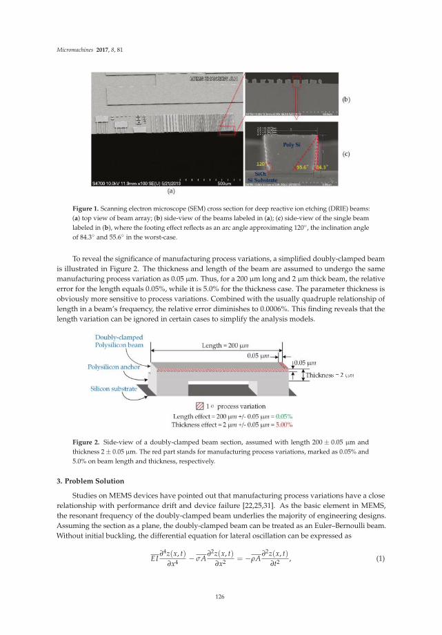
Micromachines 2017, 8, 81
Figure 1. Scanning electron microscope (SEM) cross section for deep reactive ion etching (DRIE) beams:(a) top view of beam array; (b) side-view of the beams labeled in (a); (c) side-view of the single beamlabeled in (b), where the footing effect reflects as an arc angle approximating 120◦, the inclination angleof 84.3◦ and 55.6◦ in the worst-case.
To reveal the significance of manufacturing process variations, a simplified doubly-clamped beamis illustrated in Figure 2. The thickness and length of the beam are assumed to undergo the samemanufacturing process variation as 0.05 µm. Thus, for a 200 µm long and 2 µm thick beam, the relativeerror for the length equals 0.05%, while it is 5.0% for the thickness case. The parameter thickness isobviously more sensitive to process variations. Combined with the usually quadruple relationship oflength in a beam’s frequency, the relative error diminishes to 0.0006%. This finding reveals that thelength variation can be ignored in certain cases to simplify the analysis models.
Figure 2. Side-view of a doubly-clamped beam section, assumed with length 200 ± 0.05 µm andthickness 2 ± 0.05 µm. The red part stands for manufacturing process variations, marked as 0.05% and5.0% on beam length and thickness, respectively.
3. Problem Solution
Studies on MEMS devices have pointed out that manufacturing process variations have a closerelationship with performance drift and device failure [22,25,31]. As the basic element in MEMS,the resonant frequency of the doubly-clamped beam underlies the majority of engineering designs.Assuming the section as a plane, the doubly-clamped beam can be treated as an Euler–Bernoulli beam.Without initial buckling, the differential equation for lateral oscillation can be expressed as
EI∂4z(x, t)
∂x4 − σA∂2z(x, t)
∂x2 = −ρA∂2z(x, t)
∂t2 , (1)
126
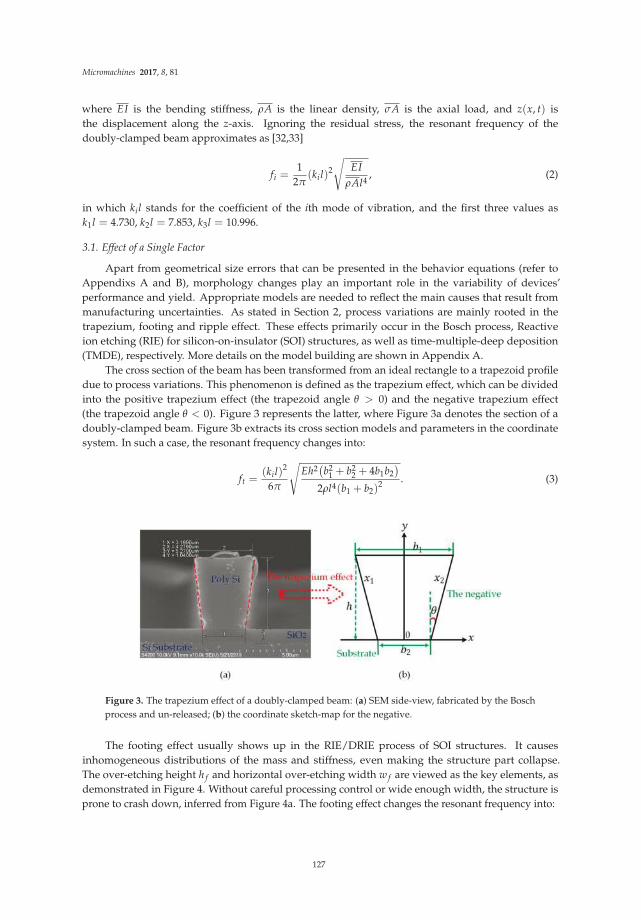
Micromachines 2017, 8, 81
where EI is the bending stiffness, ρA is the linear density, σA is the axial load, and z(x, t) isthe displacement along the z-axis. Ignoring the residual stress, the resonant frequency of thedoubly-clamped beam approximates as [32,33]
fi =1
2π(kil)
2
√
EI
ρAl4, (2)
in which kil stands for the coefficient of the ith mode of vibration, and the first three values ask1l = 4.730, k2l = 7.853, k3l = 10.996.
3.1. Effect of a Single Factor
Apart from geometrical size errors that can be presented in the behavior equations (refer toAppendixs A and B), morphology changes play an important role in the variability of devices’performance and yield. Appropriate models are needed to reflect the main causes that result frommanufacturing uncertainties. As stated in Section 2, process variations are mainly rooted in thetrapezium, footing and ripple effect. These effects primarily occur in the Bosch process, Reactiveion etching (RIE) for silicon-on-insulator (SOI) structures, as well as time-multiple-deep deposition(TMDE), respectively. More details on the model building are shown in Appendix A.
The cross section of the beam has been transformed from an ideal rectangle to a trapezoid profiledue to process variations. This phenomenon is defined as the trapezium effect, which can be dividedinto the positive trapezium effect (the trapezoid angle θ > 0) and the negative trapezium effect(the trapezoid angle θ < 0). Figure 3 represents the latter, where Figure 3a denotes the section of adoubly-clamped beam. Figure 3b extracts its cross section models and parameters in the coordinatesystem. In such a case, the resonant frequency changes into:
ft =(kil)
2
6π
√
Eh2(
b21 + b2
2 + 4b1b2)
2ρl4(b1 + b2)2 . (3)
Figure 3. The trapezium effect of a doubly-clamped beam: (a) SEM side-view, fabricated by the Boschprocess and un-released; (b) the coordinate sketch-map for the negative.
The footing effect usually shows up in the RIE/DRIE process of SOI structures. It causesinhomogeneous distributions of the mass and stiffness, even making the structure part collapse.The over-etching height h f and horizontal over-etching width w f are viewed as the key elements, asdemonstrated in Figure 4. Without careful processing control or wide enough width, the structure isprone to crash down, inferred from Figure 4a. The footing effect changes the resonant frequency into:
127
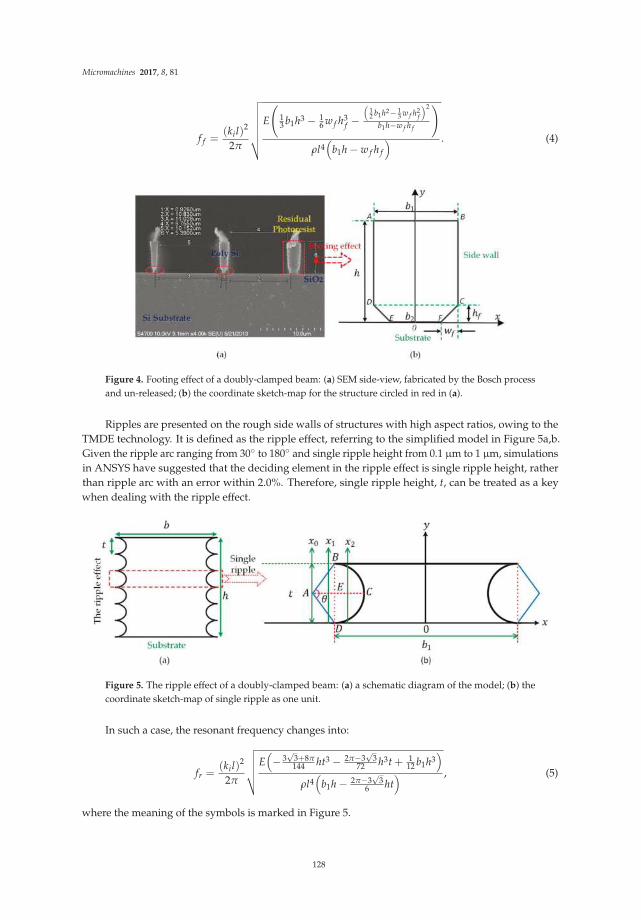
Micromachines 2017, 8, 81
f f =(kil)
2
2π
√
√
√
√
√
√
√
E
(
13 b1h3 − 1
6 w f h3f −
(
12 b1h2− 1
3 w f h2f
)2
b1h−w f h f
)
ρl4(
b1h − w f h f
) . (4)
Figure 4. Footing effect of a doubly-clamped beam: (a) SEM side-view, fabricated by the Bosch processand un-released; (b) the coordinate sketch-map for the structure circled in red in (a).
Ripples are presented on the rough side walls of structures with high aspect ratios, owing to theTMDE technology. It is defined as the ripple effect, referring to the simplified model in Figure 5a,b.Given the ripple arc ranging from 30◦ to 180◦ and single ripple height from 0.1 µm to 1 µm, simulationsin ANSYS have suggested that the deciding element in the ripple effect is single ripple height, ratherthan ripple arc with an error within 2.0%. Therefore, single ripple height, t, can be treated as a keywhen dealing with the ripple effect.
Figure 5. The ripple effect of a doubly-clamped beam: (a) a schematic diagram of the model; (b) thecoordinate sketch-map of single ripple as one unit.
In such a case, the resonant frequency changes into:
fr =(kil)
2
2π
√
√
√
√
√
E(
−3√
3+8π144 ht3 − 2π−3
√3
72 h3t + 112 b1h3
)
ρl4(
b1h − 2π−3√
36 ht
) , (5)
where the meaning of the symbols is marked in Figure 5.
128
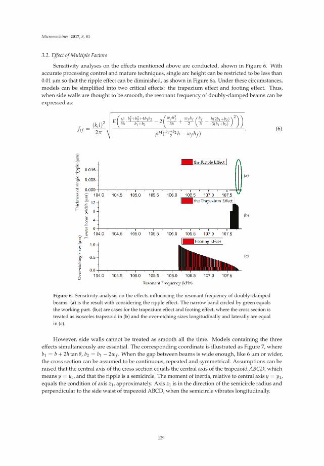
Micromachines 2017, 8, 81
3.2. Effect of Multiple Factors
Sensitivity analyses on the effects mentioned above are conducted, shown in Figure 6. Withaccurate processing control and mature techniques, single arc height can be restricted to be less than0.01 µm so that the ripple effect can be diminished, as shown in Figure 6a. Under these circumstances,models can be simplified into two critical effects: the trapezium effect and footing effect. Thus,when side walls are thought to be smooth, the resonant frequency of doubly-clamped beams can beexpressed as:
ft f =(kil)
2
2π
√
√
√
√
√
√
E
(
h3
36 ·b2
1+b22+4b1b2
b1+b2− 2
(
w f h3f
36 +w f h f
2
(
h f
3 −h(2b1+b2)3(b1+b2)
)2))
ρl4( b1+b22 h − w f h f )
. (6)
Figure 6. Sensitivity analysis on the effects influencing the resonant frequency of doubly-clampedbeams. (a) is the result with considering the ripple effect. The narrow band circled by green equalsthe working part. (b,c) are cases for the trapezium effect and footing effect, where the cross section istreated as isosceles trapezoid in (b) and the over-etching sizes longitudinally and laterally are equalin (c).
However, side walls cannot be treated as smooth all the time. Models containing the threeeffects simultaneously are essential. The corresponding coordinate is illustrated as Figure 7, whereb1 = b + 2h tan θ, b2 = b1 − 2w f . When the gap between beams is wide enough, like 6 µm or wider,the cross section can be assumed to be continuous, repeated and symmetrical. Assumptions can beraised that the central axis of the cross section equals the central axis of the trapezoid ABCD, whichmeans y = yc, and that the ripple is a semicircle. The moment of inertia, relative to central axis y = y1,equals the condition of axis z1, approximately. Axis z1 is in the direction of the semicircle radius andperpendicular to the side waist of trapezoid ABCD, when the semicircle vibrates longitudinally.
129
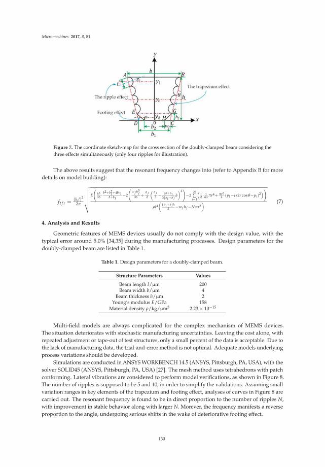
Micromachines 2017, 8, 81
Figure 7. The coordinate sketch-map for the cross section of the doubly-clamped beam considering thethree effects simultaneously (only four ripples for illustration).
The above results suggest that the resonant frequency changes into (refer to Appendix B for moredetails on model building):
ft f r =(ki l)
2
2π
√
√
√
√
√
√
E
(
h336 ·
b2+b21+4bb1
b+b1−2
(
w f h3f
36 +A f2
(
h f3 −
2b+b13(b1+b)
h
)2)
−2N∑
i=1
(
12 ·
164 πr4+ πr2
2 (y1−i∗2r cos θ−yc)2)
)
ρl4(
(b1+b)h2 −w f h f −Nπr2
) (7)
4. Analysis and Results
Geometric features of MEMS devices usually do not comply with the design value, with thetypical error around 5.0% [34,35] during the manufacturing processes. Design parameters for thedoubly-clamped beam are listed in Table 1.
Table 1. Design parameters for a doubly-clamped beam.
Structure Parameters Values
Beam length l/µm 200Beam width b/µm 4
Beam thickness h/µm 2Young’s modulus E/GPa 158
Material density ρ/kg/µm3 2.23 × 10⁻¹⁵
Multi-field models are always complicated for the complex mechanism of MEMS devices.The situation deteriorates with stochastic manufacturing uncertainties. Leaving the cost alone, withrepeated adjustment or tape-out of test structures, only a small percent of the data is acceptable. Due tothe lack of manufacturing data, the trial-and-error method is not optimal. Adequate models underlyingprocess variations should be developed.
Simulations are conducted in ANSYS WORKBENCH 14.5 (ANSYS, Pittsburgh, PA, USA), with thesolver SOLID45 (ANSYS, Pittsburgh, PA, USA) [27]. The mesh method uses tetrahedrons with patchconforming. Lateral vibrations are considered to perform model verifications, as shown in Figure 8.The number of ripples is supposed to be 5 and 10, in order to simplify the validations. Assuming smallvariation ranges in key elements of the trapezium and footing effect, analyses of curves in Figure 8 arecarried out. The resonant frequency is found to be in direct proportion to the number of ripples N,with improvement in stable behavior along with larger N. Morever, the frequency manifests a reverseproportion to the angle, undergoing serious shifts in the wake of deteriorative footing effect.
130
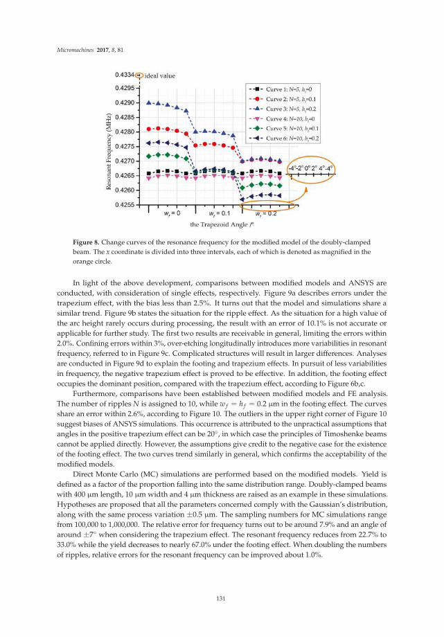
Micromachines 2017, 8, 81
Figure 8. Change curves of the resonance frequency for the modified model of the doubly-clampedbeam. The x coordinate is divided into three intervals, each of which is denoted as magnified in theorange circle.
In light of the above development, comparisons between modified models and ANSYS areconducted, with consideration of single effects, respectively. Figure 9a describes errors under thetrapezium effect, with the bias less than 2.5%. It turns out that the model and simulations share asimilar trend. Figure 9b states the situation for the ripple effect. As the situation for a high value ofthe arc height rarely occurs during processing, the result with an error of 10.1% is not accurate orapplicable for further study. The first two results are receivable in general, limiting the errors within2.0%. Confining errors within 3%, over-etching longitudinally introduces more variabilities in resonantfrequency, referred to in Figure 9c. Complicated structures will result in larger differences. Analysesare conducted in Figure 9d to explain the footing and trapezium effects. In pursuit of less variabilitiesin frequency, the negative trapezium effect is proved to be effective. In addition, the footing effectoccupies the dominant position, compared with the trapezium effect, according to Figure 6b,c.
Furthermore, comparisons have been established between modified models and FE analysis.The number of ripples N is assigned to 10, while w f = h f = 0.2 µm in the footing effect. The curvesshare an error within 2.6%, according to Figure 10. The outliers in the upper right corner of Figure 10suggest biases of ANSYS simulations. This occurrence is attributed to the unpractical assumptions thatangles in the positive trapezium effect can be 20◦, in which case the principles of Timoshenke beamscannot be applied directly. However, the assumptions give credit to the negative case for the existenceof the footing effect. The two curves trend similarly in general, which confirms the acceptability of themodified models.
Direct Monte Carlo (MC) simulations are performed based on the modified models. Yield isdefined as a factor of the proportion falling into the same distribution range. Doubly-clamped beamswith 400 µm length, 10 µm width and 4 µm thickness are raised as an example in these simulations.Hypotheses are proposed that all the parameters concerned comply with the Gaussian’s distribution,along with the same process variation ±0.5 µm. The sampling numbers for MC simulations rangefrom 100,000 to 1,000,000. The relative error for frequency turns out to be around 7.9% and an angle ofaround ±7◦ when considering the trapezium effect. The resonant frequency reduces from 22.7% to33.0% while the yield decreases to nearly 67.0% under the footing effect. When doubling the numbersof ripples, relative errors for the resonant frequency can be improved about 1.0%.
131
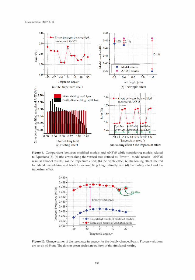
Micromachines 2017, 8, 81
Figure 9. Comparisons between modified models and ANSYS while considering models relatedto Equations (3)–(6) (the errors along the vertical axis defined as: Error = |model results—ANSYSresults|/model results): (a) the trapezium effect; (b) the ripple effect; (c) the footing effect, the redfor lateral over-etching and black for over-etching longitudinally; and (d) the footing effect and thetrapezium effect.
Figure 10. Change curves of the resonance frequency for the doubly-clamped beam. Process variationsare set as ±0.5 µm. The dots in green circles are outliers of the simulated results.
132
Micromachines 2017, 8, 81
5. Conclusions
This paper has considered the problems existing in the Bosch process and their negative influenceson MEMS doubly-clamped beam performance. Modified models of doubly-clamped beams werebuilt, with consideration for the trapezium, footing, and ripple effects respectively and simultaneously.The relative performance error was restricted to 10.0%, with a yield of about 77.3% if process variationswere assumed to be in the same range. FE verifications have been performed to validate the modelsbuilt in this study, indicating that the heavy simulation work can be substituted in some cases byapplying the models.
The model results can be viewed as the guidance for design cycle optimizations. Designers candirectly figure out the key elements in the etching process by reconsidering the design sizes and shapes,and eventually compensate the errors brought by process variations to improve the yield.
Other critical elements such as residual stress, gaps between beams, or variations in Young’smodulus were not considered in this paper and will be discussed in future work. Moreover, diversifieddistribution forms such as quasi-Gaussian can be applied in MC methods and will be the focus offuture research.
Acknowledgments: The authors would like to acknowledge the support offered by the National High TechnologyDevelopment Program of China under Contract 2015AA042604.
Author Contributions: Lili Gao developed the model, and Lili Gao and Zai-Fa Zhou jointly performed thesimulations and the data analysis. Qing-An Huang proposed the idea for the model and edited this manuscript.
Conflicts of Interest: The authors declare no conflict of interest.
Appendix A. Single Factor Effect
Appendix A.1. The Trapezium Effect
During the DRIE processes, the ideal rectangle profile of a beam can be transferred to a trapezoidprofile due to process variations. Usually, the cases are divided into the positive trapezium effect(the trapezoid angle θ > 0) and the negative trapezium effect (the trapezoid angle θ < 0), shown inFigure 3. For the ideal doubly-clamped beam, the resonance frequency can be expressed as:
f =(kil)
2
4π
√
Ew2
3ρl4 . (A1)
Inducing x-y coordinates (the same way for the positive), the upper width b1 is:
b1 = b2 − 2h· tan θ. (A2)
The neutral axis could be denoted by yna, along with the linear equations of x1 and x2, that is:
yna =Sz
At=
2b1 + b2
3(b1 + b2)h. (A3)
Here, Sz is the static moment, and At is the current cross-sectional area.Then, the moment of inertia is expressed as:
It =∫
Ay2dA ==
h3(
b21 + b2
2 + 4b1b2)
36(b1 + b2). (A4)
Thus, the resonant frequency of the doubly-clamped beam for the modified model consideringthe trapezoid effect changes into:
133

Micromachines 2017, 8, 81
ft =(kil)
2
6π
√
Eh2(
b21 + b2
2 + 4b1b2)
2ρl4(b1 + b2)2 . (A5)
Appendix A.2. The Footing Effect
The critical element in the footing effect is the over-etching height h f and horizontal over-etchingwidth w f , as shown in Figure 4. According to the properties for the moment of inertia, the moment ofinertia relative to the neutral axis for the cross section ABCFED can be expressed as:
I′ABCFED = I′ABCD + I′CDEF, (A6)
where
I′ABCD =112
b1
(
h − h f
)3, (A7)
I′CDEF =h3
f
36(
b1 − w f
) (3b21 − 6b1w f + 2w2
f ). (A8)
Then, regards to the parallel-axis theorem, the moment of inertia relative to the neutral axis yc forthe cross section ABCFED becomes
I f = IABCFED = IABCD + ICDEF = I′ABCD + b1
(
h − h f
)
(yc − y1)2 + I′CDEF + h f
(
b1 − w f
)
(yc − y2)2. (A9)
Here, y1 and y2 denote the neutral axis of ABCD and CDEF, relative to each own centroid,respectively, and
y1 =h + h f
2, y2 =
3b1 − 2w f
26b1 − 6w fh f , yc =
12 b1h2
−13 w f h2
f
b1h − w f h f. (A10)
Thus, the frequency of the doubly-clamped beam for the modified model considering the footingeffect changes into:
f f =(kil)
2
2π
√
√
√
√
√
√
√
E
(
13 b1h3 − 1
6 w f h3f −
(
12 b1h2− 1
3 w f h2f
)2
b1h−w f h f
)
ρl4(
b1h − w f h f
) . (A11)
Appendix A.3. The Ripple Effect
The key element of the ripple effect is the height of the ripple, almost nothing to do with the arcof the ripple. Therefore, the height of the ripple, t, is taken as an impact factor of the ripple effectshown as Figure 5. The impacts on frequency mainly arise from t, and the central angle is chosen asθ = 60
◦
, according to the statistical results of tapeout (for the further model optimization, θ could betreated as an independent variable). Similar to the knowledge of moment of inetia, the cross sectionregarding x = 0 under the ripple effect is the sum of each unit, depicted in Figure 5. Symetrically,the moment of inertia of each unit stays the same, regarding the axis of x = 0, denoted as I0. Here,
we have AB = AD = BD = r = t, AE =√
32 r, CE = r −
√3
2 r.With a series of calculations, the moment of inertia relative to the neutral axis itself for one unit is:
I0 =b1t3
12+
√3 − 4π
48t4. (A12)
Similarly, the sum of the moment of inertia under the ripple effect is expressed as:
Ir = ∑ Ii = ∑i=Ni=1
(
I0 +(
h2 − 2i−1
2 t)2(
b1t − 2π−3√
36 t2
)
)
= − 3√
3+8π144 ht3 − 2π−3
√3
72 h3t + 112 b1h3. (A13)
134
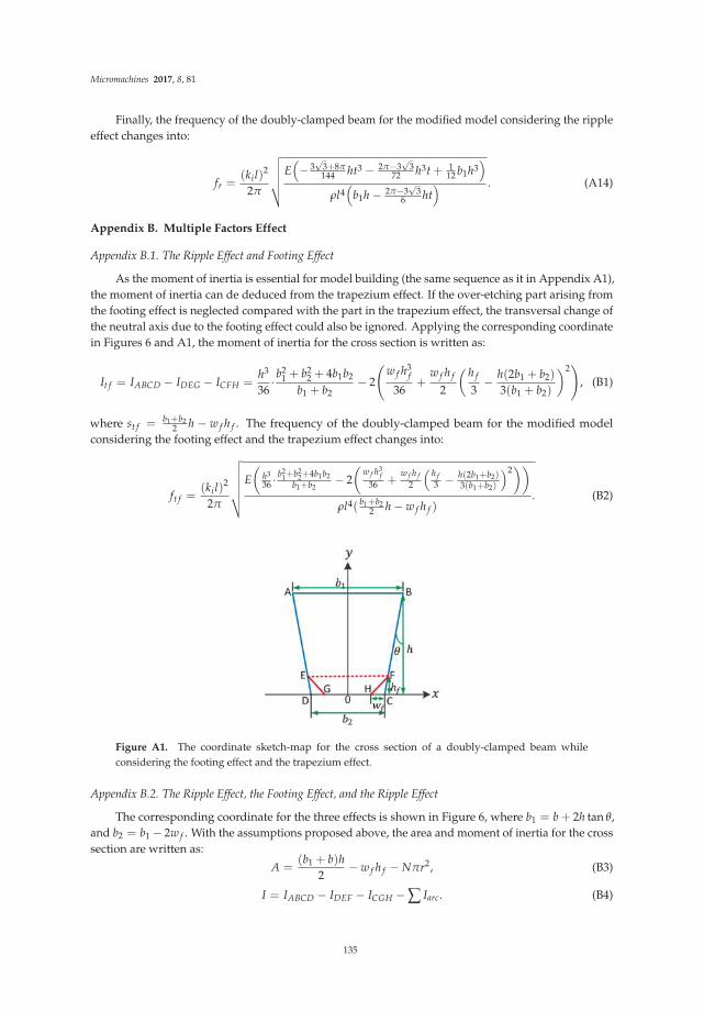
Micromachines 2017, 8, 81
Finally, the frequency of the doubly-clamped beam for the modified model considering the rippleeffect changes into:
fr =(kil)
2
2π
√
√
√
√
√
E(
−3√
3+8π144 ht3 − 2π−3
√3
72 h3t + 112 b1h3
)
ρl4(
b1h − 2π−3√
36 ht
) . (A14)
Appendix B. Multiple Factors Effect
Appendix B.1. The Ripple Effect and Footing Effect
As the moment of inertia is essential for model building (the same sequence as it in Appendix A1),the moment of inertia can de deduced from the trapezium effect. If the over-etching part arising fromthe footing effect is neglected compared with the part in the trapezium effect, the transversal change ofthe neutral axis due to the footing effect could also be ignored. Applying the corresponding coordinatein Figures 6 and A1, the moment of inertia for the cross section is written as:
It f = IABCD − IDEG − ICFH =h3
36·b2
1 + b22 + 4b1b2
b1 + b2− 2
(
w f h3f
36+
w f h f
2
(
h f
3−
h(2b1 + b2)
3(b1 + b2)
)2)
, (B1)
where st f = b1+b22 h − w f h f . The frequency of the doubly-clamped beam for the modified model
considering the footing effect and the trapezium effect changes into:
ft f =(kil)
2
2π
√
√
√
√
√
√
E
(
h3
36 ·b2
1+b22+4b1b2
b1+b2− 2
(
w f h3f
36 +w f h f
2
(
h f
3 −h(2b1+b2)3(b1+b2)
)2))
ρl4( b1+b22 h − w f h f )
. (B2)
Figure A1. The coordinate sketch-map for the cross section of a doubly-clamped beam whileconsidering the footing effect and the trapezium effect.
Appendix B.2. The Ripple Effect, the Footing Effect, and the Ripple Effect
The corresponding coordinate for the three effects is shown in Figure 6, where b1 = b + 2h tan θ,and b2 = b1 − 2w f . With the assumptions proposed above, the area and moment of inertia for the crosssection are written as:
A =(b1 + b)h
2− w f h f − Nπr2, (B3)
I = IABCD − IDEF − ICGH − ∑ Iarc. (B4)
135
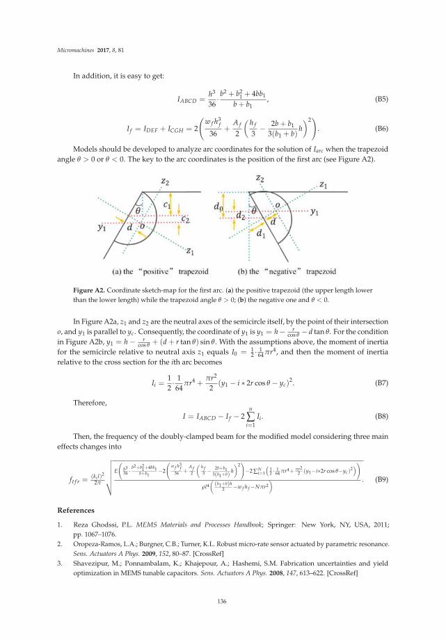
Micromachines 2017, 8, 81
In addition, it is easy to get:
IABCD =h3
36·b2 + b2
1 + 4bb1
b + b1, (B5)
I f = IDEF + ICGH = 2
(
w f h3f
36+
A f
2
(
h f
3−
2b + b1
3(b1 + b)h
)2)
. (B6)
Models should be developed to analyze arc coordinates for the solution of Iarc when the trapezoidangle θ > 0 or θ < 0. The key to the arc coordinates is the position of the first arc (see Figure A2).
Figure A2. Coordinate sketch-map for the first arc. (a) the positive trapezoid (the upper length lowerthan the lower length) while the trapezoid angle θ > 0; (b) the negative one and θ < 0.
In Figure A2a, z1 and z2 are the neutral axes of the semicircle itself, by the point of their intersectiono, and y1 is parallel to yc. Consequently, the coordinate of y1 is y1 = h− r
cos θ − d tan θ. For the conditionin Figure A2b, y1 = h −
rcos θ + (d + r tan θ) sin θ. With the assumptions above, the moment of inertia
for the semicircle relative to neutral axis z1 equals I0 = 12 ·
164 πr4, and then the moment of inertia
relative to the cross section for the ith arc becomes
Ii =12·
164
πr4 +πr2
2(y1 − i ∗ 2r cos θ − yc)
2. (B7)
Therefore,
I = IABCD − I f − 2n
∑i=1
Ii. (B8)
Then, the frequency of the doubly-clamped beam for the modified model considering three maineffects changes into
ft f r =(ki l)
2
2π
√
√
√
√
√
√
E
(
h336 ·
b2+b21+4bb1
b+b1−2
(
w f h3f
36 +A f2
(
h f3 −
2b+b13(b1+b)
h
)2)
−2 ∑Ni=1
(
12 ·
164 πr4+ πr2
2 (y1−i∗2r cos θ−yc)2)
)
ρl4(
(b1+b)h2 −w f h f −Nπr2
) . (B9)
References
1. Reza Ghodssi, P.L. MEMS Materials and Processes Handbook; Springer: New York, NY, USA, 2011;
pp. 1067–1076.
2. Oropeza-Ramos, L.A.; Burgner, C.B.; Turner, K.L. Robust micro-rate sensor actuated by parametric resonance.
Sens. Actuators A Phys. 2009, 152, 80–87. [CrossRef]
3. Shavezipur, M.; Ponnambalam, K.; Khajepour, A.; Hashemi, S.M. Fabrication uncertainties and yield
optimization in MEMS tunable capacitors. Sens. Actuators A Phys. 2008, 147, 613–622. [CrossRef]
136

Micromachines 2017, 8, 81
4. Lee, M.C.; Kang, S.J.; Jung, K.D.; Choa, S.-H.; Cho, Y.C. A high yield rate MEMS gyroscope with a packaged
siog process. J. Micromech. Microeng. 2005, 15, 2003. [CrossRef]
5. Yeom, J.; Wu, Y.; Selby, J.C.; Shannon, M.A. Maximum achievable aspect ratio in deep reactive ion etching of
silicon due to aspect ratio dependent transport and the microloading effect. J. Vac. Sci. Technol. B 2005, 23,
2319–2329. [CrossRef]
6. Johnson, B.N.; Mutharasan, R. Biosensing using dynamic-mode cantilever sensors: A review.
Biosens. Bioelectron. 2012, 32, 1–18. [CrossRef] [PubMed]
7. Lang, W. Silicon microstructuring technology. Mater. Sci. Eng. R Rep. 1996, 17, 1–55. [CrossRef]
8. Younis, M.I. MEMS Linear and Nonlinear Statics and Dynamics; Springer: New York, NY, USA, 2010; p. 453.
9. Milor, L. A survey of yield modeling and yield enhancement methods. IEEE Trans. Semicond. Manuf. 2013,
26, 196–213. [CrossRef]
10. Islam, M.F.; Ali, M.A.M.; Majlis, B.Y. Probabilistic analysis of micro-machined fixed-fixed beam for reliability.
IET Micro Nano Lett. 2008, 3, 95–100. [CrossRef]
11. Liu, M.; Maute, K.; Frangopol, D.M. Multi-objective design optimization of electrostatically actuated
microbeam resonators with and without parameter uncertainty. Reliab. Eng. Syst. Saf. 2007, 92, 1333–1343.
[CrossRef]
12. Rong, L.; Paden, B.; Turner, K. MEMS resonators that are robust to process-induced feature width variations.
J. Microelectromech. Syst. 2002, 11, 505–511. [CrossRef]
13. Mawardi, A.; Pitchumani, R. Design of microresonators under uncertainty. J. Microelectromech. Syst. 2005, 14,
63–69. [CrossRef]
14. Bagherinia, M.; Bruggi, M.; Corigliano, A.; Mariani, S.; Lasalandra, E. Geometry optimization of a lorentz
force, resonating MEMS magnetometer. Microelectron. Reliab. 2014, 54, 1192–1199. [CrossRef]
15. Luo, Z.; Wang, X.; Jin, M.; Liu, S. MEMS gyroscope yield simulation based on Monte Carlo method. In
Proceedings of the 2012 IEEE 62nd Electronic Components and Technology Conference, 29 May–1 June 2012;
pp. 1636–1639.
16. Mirzazadeh, R.; Eftekhar Azam, S.; Mariani, S. Micromechanical characterization of polysilicon films through
on-chip tests. Sensors 2016, 16, 1191. [CrossRef] [PubMed]
17. Mirzazadeh, R.G.A.; Mariani, S. Assessment of overetch and polysilicon film properties through on-chip
tests. In Proceedings of the 2nd International Electronic Conference on Sensors and Applications, Basel,
Switzerland, 15–30 November 2015.
18. Mirzazadeh, R.M.S. Assessment of micromechanically-induced uncertainties in the electromechanical
response of MEMS devices. In Proceedings of the 3rd International Electronic Conference on Sensors
and Applications, Basel, Switzerland, 15–30 November 2016.
19. Shavezipur, M.; Ponnambalam, K.; Hashemi, S.M.; Khajepour, A. A probabilistic design optimization for
MEMS tunable capacitors. Microelectron. J. 2008, 39, 1528–1533. [CrossRef]
20. Allen, M.; Raulli, M.; Maute, K.; Frangopol, D.M. Reliability-based analysis and design optimization of
electrostatically actuated MEMS. Comput. Struct. 2004, 82, 1007–1020. [CrossRef]
21. Pfingsten, T.; Herrmann, D.J.L.; Rasmussen, C.E. Model-based design analysis and yield optimization.
IEEE Trans. Semicond. Manuf. 2006, 19, 475–486. [CrossRef]
22. Vudathu, S.P.; Duganapalli, K.K.; Laur, R.; Kubalinska, D.; Bunse-Gerstner, A. Yield analysis via induction of
process statistics into the design of MEMS and other microsystems. Microsyst. Technol. 2007, 13, 1545–1551.
[CrossRef]
23. Engesser, M.; Buhmann, A.; Franke, A.R.; Korvink, J.G. Efficient reliability-based design optimization for
microelectromechanical systems. IEEE Sens. J. 2010, 10, 1383–1390. [CrossRef]
24. Agarwal, N.; Aluru, N.R. Stochastic modeling of coupled electromechanical interaction for uncertainty
quantification in electrostatically actuated MEMS. Comput. Methods Appl. Mech. Eng. 2008, 197, 3456–3471.
[CrossRef]
25. Dewey, A.; Ren, H.; Zhang, T. Behavioral modeling of microelectromechanical systems (MEMS) with
statistical performance-variability reduction and sensitivity analysis. IEEE Trans. Circuits Syst. II Analog
Digit. Signal Process. 2000, 47, 105–113. [CrossRef]
26. Vudathu, S.P.; Laur, R. A design methodology for the yield enhancement of MEMS designs with respect to
process induced variations. In Proceedings of the 57th Electronic Components and Technology Conference,
Sparks, NV, USA, 29 May–1 June 2007.
137

Micromachines 2017, 8, 81
27. ANSYS Academic Research, Release 16.2, Help System, ANSYS, Inc. Available online: http://ansys.com/
products/academic (accessed on 3 March 2017).
28. Laermer, F.; Schilp, A. Method of Anisotropically Etching Silicon. U.S. Patent US5501893, 26 March 1996.
29. Laermer, F.; Schilp, A. Method for Anisotropic Etching of Silicon. U.S. Patent US6284148, 4 September 2001.
30. Laermer, F.; Schilp, A. Method of Anisotropic Etching of Silicon. U.S. Patent US6531068, 11 March 2003.
31. Wu, B. A statistically optimal macromodeling framework with application in process variation analysis of
MEMS devices. In Proceedings of the 2012 IEEE 10th International New Circuits and Systems Conference
(NEWCAS), Montreal, QC, Canada, 17–20 June 2012; pp. 221–224.
32. Liu, C. Foundations of MEMS; Prentice Hall Press: Upper Saddle River, NJ, USA, 2011; p. 560.
33. Weaver, W., Jr.; Timoshenko, S.P.; Young, D.H. Vibration Problems in Engineering; Wiley: New York, NY, USA,
1974; pp. 415–455.
34. Cowen, A.; Hardy, B.; Mahadevan, R.; Wilcenski, S. PolyMUMPs Design Handbook; MEMSCAP Inc.: Durham,
NC, USA, 2011.
35. Cowen, A.; Hames, G.; Monk, D.; Wilcenski, S.; Hardy, B. SoiMUMPs Design Handbook; MEMSCAP Inc.:
Durham, NC, USA, 2011.
© 2017 by the authors. Licensee MDPI, Basel, Switzerland. This article is an open access
article distributed under the terms and conditions of the Creative Commons Attribution
(CC BY) license (http://creativecommons.org/licenses/by/4.0/).
138
micromachines
Article
Low Temperature Plasma Nitriding of Inner Surfacesin Stainless Steel Mini-/Micro-Pipes and Nozzles
Tatsuhiko Aizawa 1,* and Kenji Wasa 2
1 Department of Engineering and Design, Shibaura Institute of Technology, 3-19-10 Shibaura, Minato-City,Tokyo 108-8548, Japan
2 Research and Development Division, TECDIA, Co., Ltd., 4-3-4 Shibaura, Minato-City, Tokyo 108-0023, Japan;[email protected]
* Correspondence: [email protected]; Tel.: +81-3-6722-2741
Academic Editors: Hans Nørgaard Hansen and Guido ToselloReceived: 9 January 2017; Accepted: 11 May 2017; Published: 13 May 2017
Abstract: Metallic miniature products have been highlighted as mini-/micro-structural componentsworking as a precise mechanism, in dispensing systems, and in medical operations. In particular, theessential mechanical parts such as pipes and nozzles have strength and hardness sufficient for ejectingviscous liquids, solders, and particles. A low-temperature plasma nitriding process was proposed asa surface treatment to improve the engineering durability of stainless steel mini-/micro-pipes andnozzles. Various analyses were performed to describe the inner nitriding process only, from the innersurface of pipes and nozzles to their depth in thickness. AISI316 pipes and AISI316/AISI304 nozzlespecimens were used to demonstrate by plasma nitriding for 14.4 ks at 693 K that their inner surfaceshad a hardness higher than 800 HV.
Keywords: micro-fabrication; mini- and micro-nozzles; stainless steels; plasma nitriding; innersurfaces; hollow cathode device; nitrogen interstitials; hardness
1. Introduction
Pipes and nozzles are typical mechanical parts for transporting gaseous and liquid media anddepositing liquid- or melt-drops onto material surfaces and interfaces in joining, soldering, anddrawing processes [1]. In cellular phones, many devices and sensors are joined onto liquid crystalpanels by adhesives, which are deposited onto the joined interface [2]. For example, digital cameraunits are integrated into cellular phones by accurately joining a series of functional parts. Dimensionalaccuracy and integrity is preserved by joining via adhesive droplets. These nozzle outlets contact andhit the joined surfaces; the stainless steel nozzles often deform and become damaged in the joiningprocess. The ruby nozzle is often selected for sufficient hardness in operation.
High-density plasma nitriding has been used for hardening metals and alloys such as stainlesssteels, tool steels, and titanium and aluminum alloys with the use of DC-biased metallic tubes (referredto here as hollow-cathode devices) [3–6]. In these processes, these metallic alloy parts and componentsare efficiently plasma-nitrided in hollow-cathode devices. For example, AISI-420 martensitic stainlesssteel die-parts have been plasma-nitrided at 673 K for 14.4 ks to have a hardness higher than1000 HV [3,7,8]. In addition, AISI304 and AISI316 stainless steel plates were also plasma-nitridedat 673 K for 14.4 ks by 70 Pa to have a nitrided layer thickness higher than 80 µm and a hardness higherthan 1400 HV, respectively [9–11].
In the present study, this surface treatment, with the use of a hollow-cathode device, was employedto harden the inner surfaces of mini-/micro-nozzles and pipes for the joining process. The innerdiameter of their through-holes ranged from 50 µm to 10 mm. The hydrogen–nitrogen mixed gas wasblown into the inlet of these nozzles. The nitrided through-hole surfaces were observed by Scanning
Micromachines 2017, 8, 157 139 www.mdpi.com/journal/micromachines
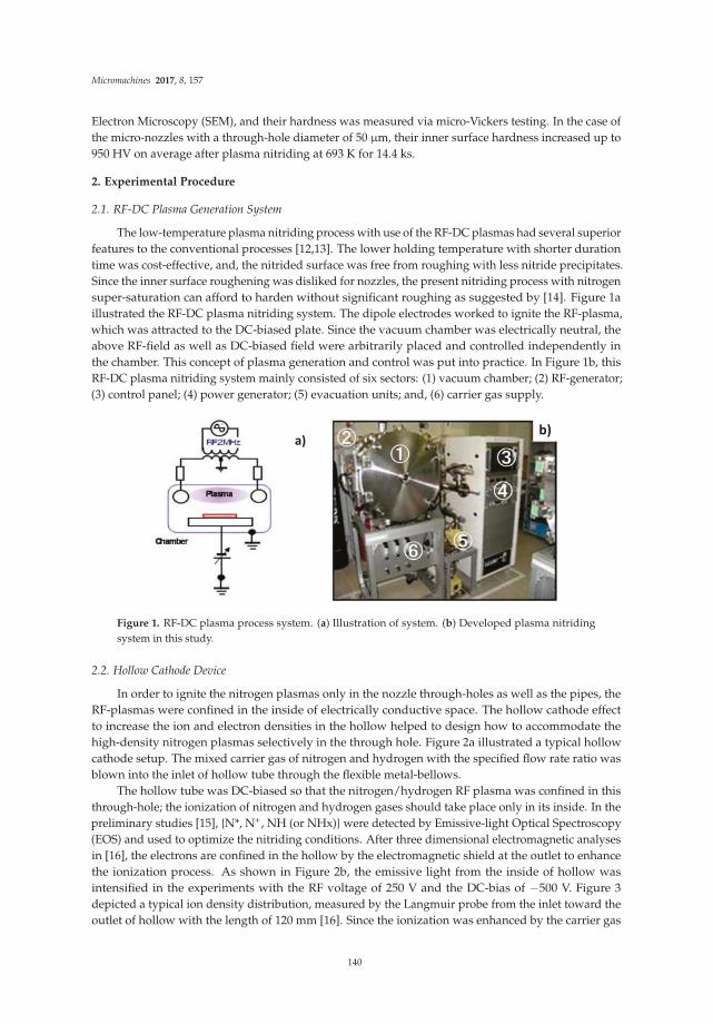
Micromachines 2017, 8, 157
Electron Microscopy (SEM), and their hardness was measured via micro-Vickers testing. In the case ofthe micro-nozzles with a through-hole diameter of 50 µm, their inner surface hardness increased up to950 HV on average after plasma nitriding at 693 K for 14.4 ks.
2. Experimental Procedure
2.1. RF-DC Plasma Generation System
The low-temperature plasma nitriding process with use of the RF-DC plasmas had several superiorfeatures to the conventional processes [12,13]. The lower holding temperature with shorter durationtime was cost-effective, and, the nitrided surface was free from roughing with less nitride precipitates.Since the inner surface roughening was disliked for nozzles, the present nitriding process with nitrogensuper-saturation can afford to harden without significant roughing as suggested by [14]. Figure 1aillustrated the RF-DC plasma nitriding system. The dipole electrodes worked to ignite the RF-plasma,which was attracted to the DC-biased plate. Since the vacuum chamber was electrically neutral, theabove RF-field as well as DC-biased field were arbitrarily placed and controlled independently inthe chamber. This concept of plasma generation and control was put into practice. In Figure 1b, thisRF-DC plasma nitriding system mainly consisted of six sectors: (1) vacuum chamber; (2) RF-generator;(3) control panel; (4) power generator; (5) evacuation units; and, (6) carrier gas supply.
a)b)
Figure 1. RF-DC plasma process system. (a) Illustration of system. (b) Developed plasma nitridingsystem in this study.
2.2. Hollow Cathode Device
In order to ignite the nitrogen plasmas only in the nozzle through-holes as well as the pipes, theRF-plasmas were confined in the inside of electrically conductive space. The hollow cathode effectto increase the ion and electron densities in the hollow helped to design how to accommodate thehigh-density nitrogen plasmas selectively in the through hole. Figure 2a illustrated a typical hollowcathode setup. The mixed carrier gas of nitrogen and hydrogen with the specified flow rate ratio wasblown into the inlet of hollow tube through the flexible metal-bellows.
The hollow tube was DC-biased so that the nitrogen/hydrogen RF plasma was confined in thisthrough-hole; the ionization of nitrogen and hydrogen gases should take place only in its inside. In thepreliminary studies [15], {N*, N+, NH (or NHx)} were detected by Emissive-light Optical Spectroscopy(EOS) and used to optimize the nitriding conditions. After three dimensional electromagnetic analysesin [16], the electrons are confined in the hollow by the electromagnetic shield at the outlet to enhancethe ionization process. As shown in Figure 2b, the emissive light from the inside of hollow wasintensified in the experiments with the RF voltage of 250 V and the DC-bias of −500 V. Figure 3depicted a typical ion density distribution, measured by the Langmuir probe from the inlet toward theoutlet of hollow with the length of 120 mm [16]. Since the ionization was enhanced by the carrier gas
140

Micromachines 2017, 8, 157
flow, the nitrogen ion density increased monotonically toward the outlet of hollow. This high densityabruptly decreased down in one or two orders just at the outside of this hollow. This ion densitydistribution was preferable to make selective nitriding of the through holes; in particular, the innersurface of nozzle outlet could be efficiently nitrided. After the Langmuir probe measurement andemissive-light optical spectroscopy, the species of activated nitrogen atoms and NHx-radicals might beresponsible for nitriding process of the austenitic stainless steel pipes and nozzles as discussed in [17].As suggested in [18], the flow rate ratio of H2 to N2 in the mixture gas also affected the NH-radicalyields in the generated plasmas. The nitriding condition with the RF voltage of 250 V, the DC-biasof −500 V, the pressure of 70 Pa and the N2/H2 ratio by 160 mL/min to 30 mL/min was used asstandard processing parameters in the following experiments. The holding temperature was measuredby the thermocouple, which was embedded in the jig to fix the pipe and nozzle on the cathode plate.The heating unit was on/off controlled to keep the measured temperature by 693 K.
DC-bias Plate
Dipole Electrode
N2 + H2
Hollow
Dipole electrode
Hollow Cathode
a) b)
Figure 2. The hollow cathode device. (a) Illustration of the hollow cathode device to ignite the nitrogenplasmas in the inside of nozzles. (b) High densification in the hollow cathode.
Figure 3. Langmuir probe measurement in the inside of hollow. (a) Experimental setup for measurement.(b) Ion density distribution from the inlet to the outlet.
2.3. Specimen
Besides for the normal AISI316 (Tokai Engineering Service Co. Ltd., Tokyo, Japan) pipe unit withthe inner diameter of 16.9 mm, both the AISI316 mini- and AISI304 micro-nozzles were prepared tomake plasma nitriding with use of the hollow cathode device. Table 1 lists their dimensional sizes andgeometries, respectively. The finished inner surfaces by mechanical machining and end-milling wasnitrided for pipe and nozzle specimens only after cleaning. The AISI316 austenitic stainless steel pipewas first used to describe the hollow cathode effect on the hardening behavior along its inner surface.
141
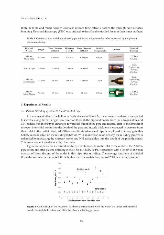
Micromachines 2017, 8, 157
Both the mini- and micro-nozzles were also utilized to selectively harden the through-hole surfaces.Scanning Electron Microscopy (SEM) was utilized to describe the nitrided layer in their inner surfaces.
Table 1. Geometry, size and dimension of pipe, mini- and micro-nozzles to be processed by the presentplasma nitriding.
Pipe andNozzle
LengthOuter Diameter
at OutletThicknessat Outlet
Inner Diameterat Outlet
SurfaceRoughness Rz
OutlookMaterialSupplier
AISI304Micro-Pipe
30.0 mm 0.88 mm 0.15 mm 0.58 mm 0.5 µm
TECDIACo., Ltd.
AISI316 Pipe 55.5 mm 21.5 mm 2.3 mm 16.9 mm 1.5 µm
TokaiEngineering
Service,Co., Ltd.
AISI316Mini-Nozzle
25.0 mm 2.8 mm 0.86 mm 1.08 mm 1.2 µm
TokaiEngineering
Service,Co., Ltd.
AISI304Micro-Nozzle
5.5 mm 1.9 mm 0.5 mm 1.0 mm 0.5 µmTECDIACo., Ltd.
3. Experimental Results
3.1. Plasma Nitriding of AISI316 Stainless Steel Pipe
In a manner similar to the hollow cathode device in Figure 2a, the nitrogen ion density is expectedto increase along the carrier gas flow direction through the pipe and nozzle since the nitrogen atom andNH–radical flux intensity is enhanced toward the outlet of the pipe and nozzle. That is, the amount ofnitrogen interstitial atoms into the depth of the pipe and nozzle thickness is expected to increase fromtheir inlet to the outlet. First, AISI316 austenitic stainless steel pipe is employed to investigate thishollow cathode effect on the nitriding behavior. With an increase in ion density, the nitriding process isenhanced by increasing the nitrogen atoms and NH–radical flux into the depth of the pipe thickness.This enhancement results in a high hardness.
Figure 4 compares the measured hardness distributions from the inlet to the outlet of the AISI316pipe before and after plasma nitriding at 693 K for 14.4 ks by 70 Pa. A specimen with a length of 16.9 mmwas cut off from the end of the outlet in this pipe after nitriding. The average hardness of nitridedthrough-hole inner surfaces is 800 HV higher than the matrix hardness of 200 HV at every position.
Displacement from the inlet, mm
0
200
400
600
800
1000
1200
1400
0 2 4 6 8 10 12 14 16 18
Nitrided nozzle
Bare nozzle
Ha
rdn
ess
, HV
0.1
Figure 4. Comparison of the measured hardness distribution toward the end of the outlet in the normalnozzle through-hole before and after the plasma nitriding process.
142
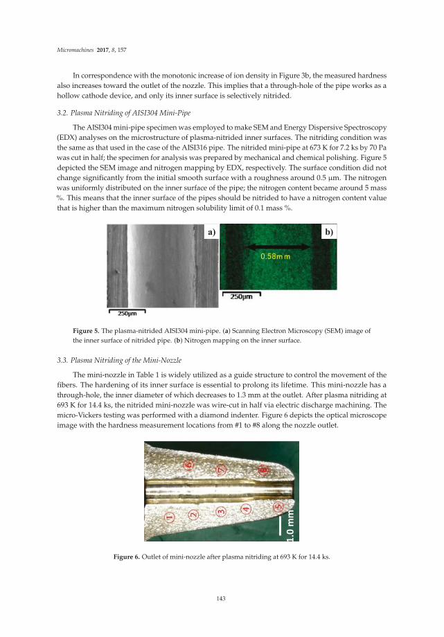
Micromachines 2017, 8, 157
In correspondence with the monotonic increase of ion density in Figure 3b, the measured hardnessalso increases toward the outlet of the nozzle. This implies that a through-hole of the pipe works as ahollow cathode device, and only its inner surface is selectively nitrided.
3.2. Plasma Nitriding of AISI304 Mini-Pipe
The AISI304 mini-pipe specimen was employed to make SEM and Energy Dispersive Spectroscopy(EDX) analyses on the microstructure of plasma-nitrided inner surfaces. The nitriding condition wasthe same as that used in the case of the AISI316 pipe. The nitrided mini-pipe at 673 K for 7.2 ks by 70 Pawas cut in half; the specimen for analysis was prepared by mechanical and chemical polishing. Figure 5depicted the SEM image and nitrogen mapping by EDX, respectively. The surface condition did notchange significantly from the initial smooth surface with a roughness around 0.5 µm. The nitrogenwas uniformly distributed on the inner surface of the pipe; the nitrogen content became around 5 mass%. This means that the inner surface of the pipes should be nitrided to have a nitrogen content valuethat is higher than the maximum nitrogen solubility limit of 0.1 mass %.
a) b)
Figure 5. The plasma-nitrided AISI304 mini-pipe. (a) Scanning Electron Microscopy (SEM) image ofthe inner surface of nitrided pipe. (b) Nitrogen mapping on the inner surface.
3.3. Plasma Nitriding of the Mini-Nozzle
The mini-nozzle in Table 1 is widely utilized as a guide structure to control the movement of thefibers. The hardening of its inner surface is essential to prolong its lifetime. This mini-nozzle has athrough-hole, the inner diameter of which decreases to 1.3 mm at the outlet. After plasma nitriding at693 K for 14.4 ks, the nitrided mini-nozzle was wire-cut in half via electric discharge machining. Themicro-Vickers testing was performed with a diamond indenter. Figure 6 depicts the optical microscopeimage with the hardness measurement locations from #1 to #8 along the nozzle outlet.
1.0
mm
Figure 6. Outlet of mini-nozzle after plasma nitriding at 693 K for 14.4 ks.
143
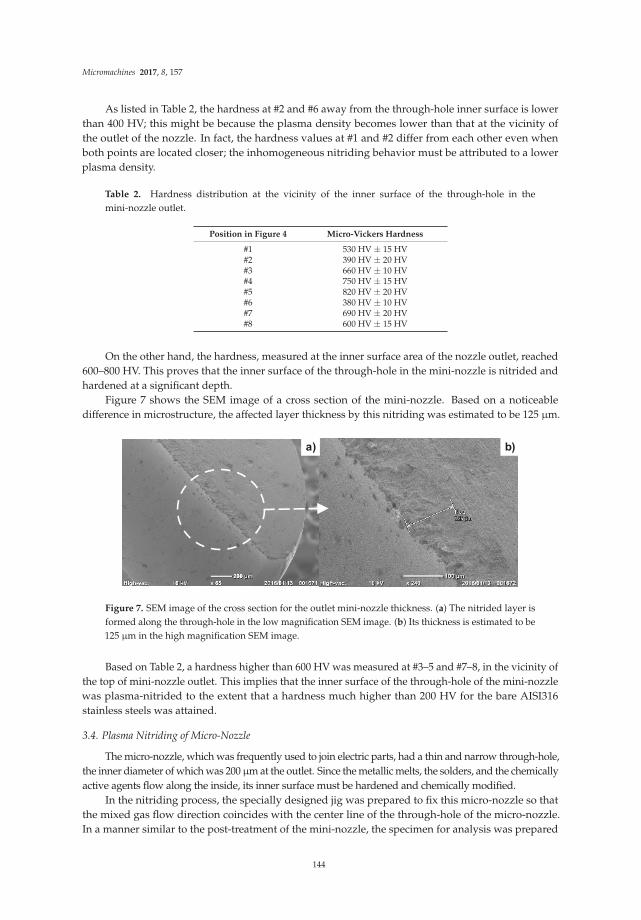
Micromachines 2017, 8, 157
As listed in Table 2, the hardness at #2 and #6 away from the through-hole inner surface is lowerthan 400 HV; this might be because the plasma density becomes lower than that at the vicinity ofthe outlet of the nozzle. In fact, the hardness values at #1 and #2 differ from each other even whenboth points are located closer; the inhomogeneous nitriding behavior must be attributed to a lowerplasma density.
Table 2. Hardness distribution at the vicinity of the inner surface of the through-hole in themini-nozzle outlet.
Position in Figure 4 Micro-Vickers Hardness
#1 530 HV ± 15 HV#2 390 HV ± 20 HV#3 660 HV ± 10 HV#4 750 HV ± 15 HV#5 820 HV ± 20 HV#6 380 HV ± 10 HV#7 690 HV ± 20 HV#8 600 HV ± 15 HV
On the other hand, the hardness, measured at the inner surface area of the nozzle outlet, reached600–800 HV. This proves that the inner surface of the through-hole in the mini-nozzle is nitrided andhardened at a significant depth.
Figure 7 shows the SEM image of a cross section of the mini-nozzle. Based on a noticeabledifference in microstructure, the affected layer thickness by this nitriding was estimated to be 125 µm.
a) b)
Figure 7. SEM image of the cross section for the outlet mini-nozzle thickness. (a) The nitrided layer isformed along the through-hole in the low magnification SEM image. (b) Its thickness is estimated to be125 µm in the high magnification SEM image.
Based on Table 2, a hardness higher than 600 HV was measured at #3–5 and #7–8, in the vicinity ofthe top of mini-nozzle outlet. This implies that the inner surface of the through-hole of the mini-nozzlewas plasma-nitrided to the extent that a hardness much higher than 200 HV for the bare AISI316stainless steels was attained.
3.4. Plasma Nitriding of Micro-Nozzle
The micro-nozzle, which was frequently used to join electric parts, had a thin and narrow through-hole,the inner diameter of which was 200µm at the outlet. Since the metallic melts, the solders, and the chemicallyactive agents flow along the inside, its inner surface must be hardened and chemically modified.
In the nitriding process, the specially designed jig was prepared to fix this micro-nozzle so thatthe mixed gas flow direction coincides with the center line of the through-hole of the micro-nozzle.In a manner similar to the post-treatment of the mini-nozzle, the specimen for analysis was prepared
144

Micromachines 2017, 8, 157
from the plasma-nitrided micro-nozzle. Figure 8 depicts the optical microscopic image of the specimenwith hardness measurement locations from #1 to #3 at the vicinity of the nozzle outlet inner surface.The positions of #1 and #2 are located at the vicinity of the inner surface of the through-hole, while #3is selected to locate only on the inner surface of the through-hole.
a) b)
500 m
Figure 8. A cross section of the plasma nitride micro-nozzle at 693 K for 14.4 ks. (a) Hardness testingspecimen cut-off from the original micro-nozzle. (b) The hardness measuring points from #1 to #3 onthe flattened surface in the specimen.
Table 3 summarizes the measured micro-Vickers hardness at #1 to #3. Compared to the hardnessof bare AISI316, 200 HV, the inner surface of the through-hole was significantly hardened. The averagehardness for this micro-nozzle was 950 HV, much higher than that for the mini-nozzle. This is becausethe micro-indenter included more un-nitrided area at the outlet of a mini-nozzle to lower the measuredhardness in practice. On the other hand, in the case of this micro-nozzle, the nitrided area of itsthickness at the outlet mainly contributes to the measured hardness.
Table 3. Hardness distribution at the vicinity of the inner surface of the through-hole in themicro-nozzle outlet.
Position in Figure 6 Micro-Vickers Hardness
#1 960 HV ± 30 HV#2 880 HV ± 20 HV#3 1020 HV ± 15 HV
Figure 9 shows the SEM image of a cross section of the outlet of the through-hole. Although thefine nitriding front end was not observed in the thickness, the deeper nitrided layer might be formedby the present hollow cathode-type plasma nitriding.
Figure 9. SEM image of a cross section at the outlet of the micro-nozzle with an inner diameter of 200 µm.
145
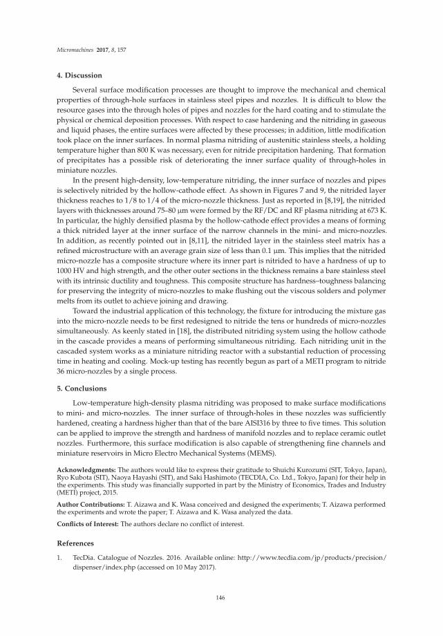
Micromachines 2017, 8, 157
4. Discussion
Several surface modification processes are thought to improve the mechanical and chemicalproperties of through-hole surfaces in stainless steel pipes and nozzles. It is difficult to blow theresource gases into the through holes of pipes and nozzles for the hard coating and to stimulate thephysical or chemical deposition processes. With respect to case hardening and the nitriding in gaseousand liquid phases, the entire surfaces were affected by these processes; in addition, little modificationtook place on the inner surfaces. In normal plasma nitriding of austenitic stainless steels, a holdingtemperature higher than 800 K was necessary, even for nitride precipitation hardening. That formationof precipitates has a possible risk of deteriorating the inner surface quality of through-holes inminiature nozzles.
In the present high-density, low-temperature nitriding, the inner surface of nozzles and pipesis selectively nitrided by the hollow-cathode effect. As shown in Figures 7 and 9, the nitrided layerthickness reaches to 1/8 to 1/4 of the micro-nozzle thickness. Just as reported in [8,19], the nitridedlayers with thicknesses around 75–80 µm were formed by the RF/DC and RF plasma nitriding at 673 K.In particular, the highly densified plasma by the hollow-cathode effect provides a means of forminga thick nitrided layer at the inner surface of the narrow channels in the mini- and micro-nozzles.In addition, as recently pointed out in [8,11], the nitrided layer in the stainless steel matrix has arefined microstructure with an average grain size of less than 0.1 µm. This implies that the nitridedmicro-nozzle has a composite structure where its inner part is nitrided to have a hardness of up to1000 HV and high strength, and the other outer sections in the thickness remains a bare stainless steelwith its intrinsic ductility and toughness. This composite structure has hardness–toughness balancingfor preserving the integrity of micro-nozzles to make flushing out the viscous solders and polymermelts from its outlet to achieve joining and drawing.
Toward the industrial application of this technology, the fixture for introducing the mixture gasinto the micro-nozzle needs to be first redesigned to nitride the tens or hundreds of micro-nozzlessimultaneously. As keenly stated in [18], the distributed nitriding system using the hollow cathodein the cascade provides a means of performing simultaneous nitriding. Each nitriding unit in thecascaded system works as a miniature nitriding reactor with a substantial reduction of processingtime in heating and cooling. Mock-up testing has recently begun as part of a METI program to nitride36 micro-nozzles by a single process.
5. Conclusions
Low-temperature high-density plasma nitriding was proposed to make surface modificationsto mini- and micro-nozzles. The inner surface of through-holes in these nozzles was sufficientlyhardened, creating a hardness higher than that of the bare AISI316 by three to five times. This solutioncan be applied to improve the strength and hardness of manifold nozzles and to replace ceramic outletnozzles. Furthermore, this surface modification is also capable of strengthening fine channels andminiature reservoirs in Micro Electro Mechanical Systems (MEMS).
Acknowledgments: The authors would like to express their gratitude to Shuichi Kurozumi (SIT, Tokyo, Japan),Ryo Kubota (SIT), Naoya Hayashi (SIT), and Saki Hashimoto (TECDIA, Co. Ltd., Tokyo, Japan) for their help inthe experiments. This study was financially supported in part by the Ministry of Economics, Trades and Industry(METI) project, 2015.
Author Contributions: T. Aizawa and K. Wasa conceived and designed the experiments; T. Aizawa performedthe experiments and wrote the paper; T. Aizawa and K. Wasa analyzed the data.
Conflicts of Interest: The authors declare no conflict of interest.
References
1. TecDia. Catalogue of Nozzles. 2016. Available online: http://www.tecdia.com/jp/products/precision/
dispenser/index.php (accessed on 10 May 2017).
146

Micromachines 2017, 8, 157
2. Resigen, U.; Scheik, S. Multi-dimensional line dispensing of unfilled adhesives. Microsyst. Technol. 2008, 14,
1895–1901. [CrossRef]
3. Katoh, T.; Aizawa, T.; Yamaguchi, T. Plasma assisted nitriding for micro-texturing martensitic stainless steels.
Manuf. Rev. 2015, 2, 2. [CrossRef]
4. Aizawa, T.; Fukuda, T.; Morita, T. Low temperature high density plasma nitriding of stainless steel molds for
stamping of oxide glasses. Manuf. Rev. 2016, 3, 2. [CrossRef]
5. Windajanti, J.M.; Aizawa, T.; Djoko, H.S. High density plasma nitriding of pure titanium. In Proceedings of
the 10th SEATUC Conference 2016, Tokyo, Japan, 22–24 February 2016.
6. Aizawa, T.; Muraishi, S.; Sugita, Y. High density plasma nitriding of Al-Cu alloys for automotive parts.
J. Phys. Sci. Appl. 2014, 4, 255–261.
7. Kim, S.K.; Yoo, J.S.; Priest, J.M.; Fewell, M.P. Characteristics of martensitic stainless steel nitrided in a
low-pressure RF plasma. Surf. Coat. Technol. 2003, 163, 380–385. [CrossRef]
8. Farghali, A.; Aizawa, T. Phase transformation induced by high nitrogen content solid solution in the
martensitic stainless steels. Mater. Trans. 2017, 58, 697–700. [CrossRef]
9. Samandi, M.; Shedden, B.A.; Smith, D.I.; Collins, G.A.; Hutchings, R.; Tendys, H. Microstructure, corrosion
and tribological behavior of plasma immersion ion-implanted austenitic stainless steel. Surf. Coat. Technol.
1993, 59, 261–266. [CrossRef]
10. Blawert, C.; Mordike, B.L.; Jiraskova, Y.; Schneeweiss, O. Structure and composition of expanded
austenite produced by nitrogen plasma immersion ion implantation of stainless steels X6CrNiTi1810 and
X2CrNiMoN2253. Surf. Coat. Technol. 1999, 116, 189–198. [CrossRef]
11. Farghali, A.; Aizawa, T. High nitrogen concentration on the fine grained austenitic stainless steels.
In Proceedings of the 11th SEATUC Conference, Ho Chi Minh City, Vietnam, 13–14 March 2017; in press.
12. Aizawa, T.; Sugita, Y. High density RF-DC plasma nitriding of steels for die and mold technologies.
Res. Rep. SIT 2013, 57, 1–10.
13. Anzai, M. Surface Treatment for High Qualification of Dies and Molds; Nikkan-Kougyo Shinbun: Tokyo, Japan, 2009.
14. Dong, H. S-phase surface engineering of Fe-Cr, Co-Cr and Ni-Cr alloys. Int. Mater. Rev. 2010, 55, 65–98. [CrossRef]
15. Santjojo, D.J.; Istiroyah; Aizawa, T. Dynamics of nitrogen and hydrogen species in a high rate plasma
nitriding of martensitic stainless steel. In Proceedings of the 9th SEATUC Conference, Nakhon Ratchasima,
Thailand, 27–30 July 2015.
16. Yunata, E.E. Characterization and Application of Hollow Cathode Oxygen Plasma. Ph.D. Thesis, Shibaura
Institute of Technology, Tokyo, Japan, 2016.
17. Czerwiec, T.; Michel, H.; Bergmann, E. Low-pressure, high-density plasma nitriding: Mechanisms,
technology and results. Surf. Coat. Technol. 1998, 108–109, 182–190. [CrossRef]
18. Aizawa, T.; Sugita, Y. Distributed plasma nitriding systems for surface treatment of miniature functional
products. In Proceedings of the 9th 4M/ICOMM, Milan, Italy, 31 March–2 April 2015; pp. 449–453.
19. Ferreira, L.M.; Brunatto, S.F.; Cardoso, R.P. Martensitic stainless steels low-temperature nitriding:
Dependence of substrate composition. Mater. Res. 2015, 18, 622–627. [CrossRef]
© 2017 by the authors. Licensee MDPI, Basel, Switzerland. This article is an open access
article distributed under the terms and conditions of the Creative Commons Attribution
(CC BY) license (http://creativecommons.org/licenses/by/4.0/).
147
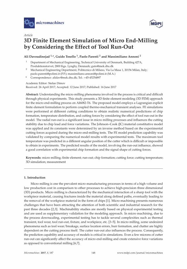
micromachines
Article
3D Finite Element Simulation of Micro End-Millingby Considering the Effect of Tool Run-Out
Ali Davoudinejad 1,*, Guido Tosello 1, Paolo Parenti 2 and Massimiliano Annoni 2
1 Department of Mechanical Engineering, Technical University of Denmark, Building 427A,Produktionstorvet, 2800 Kgs. Lyngby, Denmark; [email protected]
2 Mechanical Engineering Department, Politecnico di Milano, Via La Masa 1, 20156 Milan, Italy;[email protected] (P.P.); [email protected] (M.A.)
* Correspondence: [email protected]; Tel.: +45-45254897
Academic Editor: Stefan DimovReceived: 26 April 2017; Accepted: 12 June 2017; Published: 16 June 2017
Abstract: Understanding the micro milling phenomena involved in the process is critical and difficultthrough physical experiments. This study presents a 3D finite element modeling (3D FEM) approachfor the micro end-milling process on Al6082-T6. The proposed model employs a Lagrangian explicitfinite element formulation to perform coupled thermo-mechanical transient analyses. FE simulationswere performed at different cutting conditions to obtain realistic numerical predictions of chipformation, temperature distribution, and cutting forces by considering the effect of tool run-out in themodel. The radial run-out is a significant issue in micro milling processes and influences the cuttingstability due to chip load and force variations. The Johnson–Cook (JC) material constitutive modelwas applied and its constants were determined by an inverse method based on the experimentalcutting forces acquired during the micro end-milling tests. The FE model prediction capability wasvalidated by comparing the numerical model results with experimental tests. The maximum tooltemperature was predicted in a different angular position of the cutter which is difficult or impossibleto obtain in experiments. The predicted results of the model, involving the run-out influence, showeda good correlation with experimental chip formation and the signal shape of cutting forces.
Keywords: micro milling; finite element; run-out; chip formation; cutting force; cutting temperature;3D simulation; measurement
1. Introduction
Micro milling is one the prevalent micro manufacturing processes in terms of a high volume andlow production cost in comparison to other processes to achieve high-precision three dimensional(3D) products. Micro milling is characterized by the mechanical interaction of a sharp tool with theworkpiece material, causing fractures inside the material along defined paths, eventually leading tothe removal of the workpiece material in the form of chips [1]. Micro machining presents numerouschallenges that have been attracting the attention of both scientific and industrial research for thepast three decades [2,3]. Machinability studies are mostly based on physical experimental testingand are used as supplementary validation for the modeling approach. In micro machining, due tothe process downscaling, experimental testing has to tackle several complexities such as thermaltransient, tool wear, tool run-out, fixture, and workpiece, etc. [3–5]. In micro milling, some undesiredphenomena such as tool wear/breakage, surface location errors, burr formation, and chatter are highlydependent on the cutting process itself. The cutter run-out also influences the process. Consequently,the prediction capability and accuracy of models is critical in simulations. Even a few microns of cutterrun-out can significantly affect the accuracy of micro end-milling and create extensive force variationsas opposed to conventional milling [6,7].
Micromachines 2017, 8, 187 148 www.mdpi.com/journal/micromachines

Micromachines 2017, 8, 187
During the last four decades, numerical modeling (Finite Element Modeling (FEM) methods)has been recognized as a viable method for reducing or eliminating trial and error approaches in thedesign and optimization of machining processes. The 2D FE model investigated the effects of threemicrogroove parameters (groove width, edge distance, and depth ratio) on the friction and wear oftextured and non-textured tools. It was revealed that microgrooves on the rake face of a cutting toolperpendicular to the chip flow direction were effective in a way that the frictional behavior at thechip–tool interface was improved. Microgrooves were also very effective in reducing flank wear andcrater wear [8].
This study reported a significant effect of temperature on the flow stress that affected the cuttingforces prediction results. A strain gradient plasticity based-FE model of orthogonal micro cuttingof Al5083-H116 was used to investigate the influence of the tool edge radius on the size effect [9].A micro orthogonal cutting simulation at small uncut chip thickness levels was presented to predict asizeable strain gradient strengthening effect that was validated through micro cutting experiments [10].Irfan et al. investigated the 2D FE modeling of Inconel 718 micro milling for different feed rates andcutting tool edge angles. A higher cutting temperature was observed at a higher feed rate and with anegative edge angle. The maximum stress distribution occurred in the contact zone between the tooland chip [11].
Afazov et al. [12] investigated micro milling force calculations using orthogonal FE methodsincluding a mathematical model for determining the uncut chip thickness in the presence of run-outeffects for AISI 4340 steel. The uncut chip thickness and the tool path trajectories were determined fordistinct micro milling parameters such as the cutting velocity, cutting tool radius, feed rate, and numberof teeth. The prediction of 2D FEM orthogonal micro cutting forces by considering the chip load andtool edge radius effect was utilized for the micro end milling of brass 260 in [13]. Tool trajectories,the edge radius, and run-out effects are considered in the prediction of milling forces. The cutting forcecoefficients were identified from a set of simulations at a range of cutting edge radii and chip loads.Another study investigated coated and uncoated cubic boron nitride (CBN) tools with the 2D finiteelement method (FEM) to predict the chip formation, cutting forces, temperatures, and wear ratesgenerated in the micro milling of Ti-6Al-4V titanium alloy. The effect of run-out was not considered inthe model [14]. 2D FEM micro-end milling of Ti-6Al-4V titanium alloy was investigated with a planestrain-based orthogonal cutting force model with a tool edge radius effect to validate the cutting forceresults [15].
Although 2D FE simulations offer some distinct advantages when studying the orthogonal cuttingprocess, 3D FE models provide more realistic oblique configurations, mainly in milling processeswith complex cutting tool geometries [16,17]. 3D FE simulations present supplementary analysiscapabilities to investigate the effect of the helix angle and tool edge radius on chip flow and burrformation, which are almost impossible to be considered by 2D FE models [18].
A 3D FE model was developed to investigate the correlation between the cutting temperatureand cutting edge radii in the micro-end milling of Al2024-T6 [19]. In this study, the simulationresults revealed that increasing the tool edge radius increases the cutting temperature, reaching thehighest temperature of 57.5 ◦C at the edge radius. Another study investigated 3D FEM to predict tooland workpiece temperature fields in the micro milling process of Ti-6Al-4V under various cuttingconditions. A thermocouple was used for the experimental temperature measurements to validatethe simulation results [20]. A 3D FEM study was developed on the same Ti-6Al-4V material in orderto investigate the cutting forces in three directions under different cutting conditions, and the chipevolution and morphologies of different cutting parameters were also analyzed. The predicted andexperimental chip morphologies were compared and a good agreement was observed. In termsof cutting forces, the predicted cutting forces showed a good correlation with the experimentallymeasured data with a 6–8% prediction error in the X- and Y-directions and a 12–15% prediction errorin the Z-direction [21].
149
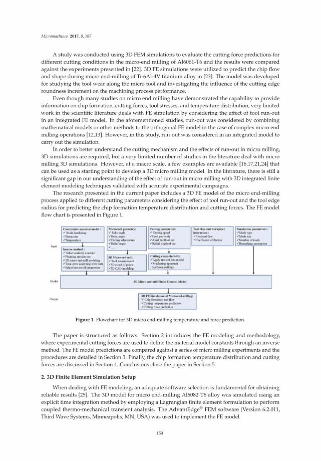
Micromachines 2017, 8, 187
A study was conducted using 3D FEM simulations to evaluate the cutting force predictions fordifferent cutting conditions in the micro-end milling of Al6061-T6 and the results were comparedagainst the experiments presented in [22]. 3D FE simulations were utilized to predict the chip flowand shape during micro end-milling of Ti-6Al-4V titanium alloy in [23]. The model was developedfor studying the tool wear along the micro tool and investigating the influence of the cutting edgeroundness increment on the machining process performance.
Even though many studies on micro end milling have demonstrated the capability to provideinformation on chip formation, cutting forces, tool stresses, and temperature distribution, very limitedwork in the scientific literature deals with FE simulation by considering the effect of tool run-outin an integrated FE model. In the aforementioned studies, run-out was considered by combiningmathematical models or other methods to the orthogonal FE model in the case of complex micro endmilling operations [12,13]. However, in this study, run-out was considered in an integrated model tocarry out the simulation.
In order to better understand the cutting mechanism and the effects of run-out in micro milling,3D simulations are required, but a very limited number of studies in the literature deal with micromilling 3D simulations. However, at a macro scale, a few examples are available [16,17,21,24] thatcan be used as a starting point to develop a 3D micro milling model. In the literature, there is still asignificant gap in our understanding of the effect of run-out in micro milling with 3D integrated finiteelement modeling techniques validated with accurate experimental campaigns.
The research presented in the current paper includes a 3D FE model of the micro end-millingprocess applied to different cutting parameters considering the effect of tool run-out and the tool edgeradius for predicting the chip formation temperature distribution and cutting forces. The FE modelflow chart is presented in Figure 1.
Figure 1. Flowchart for 3D micro end-milling temperature and force prediction.
The paper is structured as follows. Section 2 introduces the FE modeling and methodology,where experimental cutting forces are used to define the material model constants through an inversemethod. The FE model predictions are compared against a series of micro milling experiments and theprocedures are detailed in Section 3. Finally, the chip formation temperature distribution and cuttingforces are discussed in Section 4. Conclusions close the paper in Section 5.
2. 3D Finite Element Simulation Setup
When dealing with FE modeling, an adequate software selection is fundamental for obtainingreliable results [25]. The 3D model for micro end-milling Al6082-T6 alloy was simulated using anexplicit time integration method by employing a Lagrangian finite element formulation to performcoupled thermo-mechanical transient analysis. The AdvantEdge® FEM software (Version 6.2.011,Third Wave Systems, Minneapolis, MN, USA) was used to implement the FE model.
150
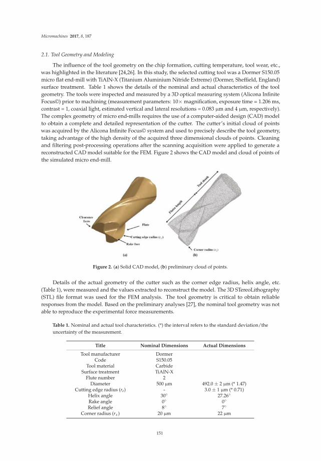
Micromachines 2017, 8, 187
2.1. Tool Geometry and Modeling
The influence of the tool geometry on the chip formation, cutting temperature, tool wear, etc.,was highlighted in the literature [24,26]. In this study, the selected cutting tool was a Dormer S150.05micro flat end-mill with TiAlN-X (Titanium Aluminium Nitride Extreme) (Dormer, Sheffield, England)surface treatment. Table 1 shows the details of the nominal and actual characteristics of the toolgeometry. The tools were inspected and measured by a 3D optical measuring system (Alicona InfiniteFocus©) prior to machining (measurement parameters: 10× magnification, exposure time = 1.206 ms,contrast = 1, coaxial light, estimated vertical and lateral resolutions = 0.083 µm and 4 µm, respectively).The complex geometry of micro end-mills requires the use of a computer-aided design (CAD) modelto obtain a complete and detailed representation of the cutter. The cutter’s initial cloud of pointswas acquired by the Alicona Infinite Focus© system and used to precisely describe the tool geometry,taking advantage of the high density of the acquired three dimensional clouds of points. Cleaningand filtering post-processing operations after the scanning acquisition were applied to generate areconstructed CAD model suitable for the FEM. Figure 2 shows the CAD model and cloud of points ofthe simulated micro end-mill.
Figure 2. (a) Solid CAD model, (b) preliminary cloud of points.
Details of the actual geometry of the cutter such as the corner edge radius, helix angle, etc.(Table 1), were measured and the values extracted to reconstruct the model. The 3D STereoLithography(STL) file format was used for the FEM analysis. The tool geometry is critical to obtain reliableresponses from the model. Based on the preliminary analyses [27], the nominal tool geometry was notable to reproduce the experimental force measurements.
Table 1. Nominal and actual tool characteristics. (*) the interval refers to the standard deviation/theuncertainty of the measurement.
Title Nominal Dimensions Actual Dimensions
Tool manufacturer DormerCode S150.05
Tool material CarbideSurface treatment TiAlN-X
Flute number 2Diameter 500 µm 492.0 ± 2 µm (* 1.47)
Cutting edge radius (re) - 3.0 ± 1 µm (* 0.71)Helix angle 30◦ 27.26◦
Rake angle 0◦ 0◦
Relief angle 8◦ 7◦
Corner radius (rε) 20 µm 22 µm
151
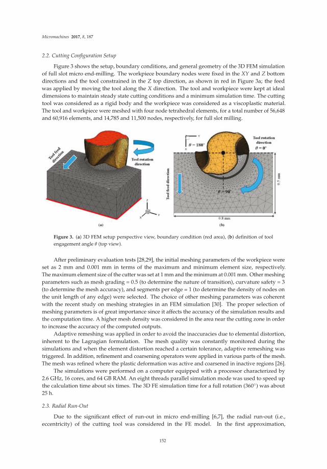
Micromachines 2017, 8, 187
2.2. Cutting Configuration Setup
Figure 3 shows the setup, boundary conditions, and general geometry of the 3D FEM simulationof full slot micro end-milling. The workpiece boundary nodes were fixed in the XY and Z bottomdirections and the tool constrained in the Z top direction, as shown in red in Figure 3a; the feedwas applied by moving the tool along the X direction. The tool and workpiece were kept at idealdimensions to maintain steady state cutting conditions and a minimum simulation time. The cuttingtool was considered as a rigid body and the workpiece was considered as a viscoplastic material.The tool and workpiece were meshed with four node tetrahedral elements, for a total number of 56,648and 60,916 elements, and 14,785 and 11,500 nodes, respectively, for full slot milling.
Figure 3. (a) 3D FEM setup perspective view, boundary condition (red area), (b) definition of toolengagement angle θ (top view).
After preliminary evaluation tests [28,29], the initial meshing parameters of the workpiece wereset as 2 mm and 0.001 mm in terms of the maximum and minimum element size, respectively.The maximum element size of the cutter was set at 1 mm and the minimum at 0.001 mm. Other meshingparameters such as mesh grading = 0.5 (to determine the nature of transition), curvature safety = 3(to determine the mesh accuracy), and segments per edge = 1 (to determine the density of nodes onthe unit length of any edge) were selected. The choice of other meshing parameters was coherentwith the recent study on meshing strategies in an FEM simulation [30]. The proper selection ofmeshing parameters is of great importance since it affects the accuracy of the simulation results andthe computation time. A higher mesh density was considered in the area near the cutting zone in orderto increase the accuracy of the computed outputs.
Adaptive remeshing was applied in order to avoid the inaccuracies due to elemental distortion,inherent to the Lagragian formulation. The mesh quality was constantly monitored during thesimulations and when the element distortion reached a certain tolerance, adaptive remeshing wastriggered. In addition, refinement and coarsening operators were applied in various parts of the mesh.The mesh was refined where the plastic deformation was active and coarsened in inactive regions [26].
The simulations were performed on a computer equipped with a processor characterized by2.6 GHz, 16 cores, and 64 GB RAM. An eight threads parallel simulation mode was used to speed upthe calculation time about six times. The 3D FE simulation time for a full rotation (360◦) was about25 h.
2.3. Radial Run-Out
Due to the significant effect of run-out in micro end-milling [6,7], the radial run-out (i.e.,eccentricity) of the cutting tool was considered in the FE model. In the first approximation,
152
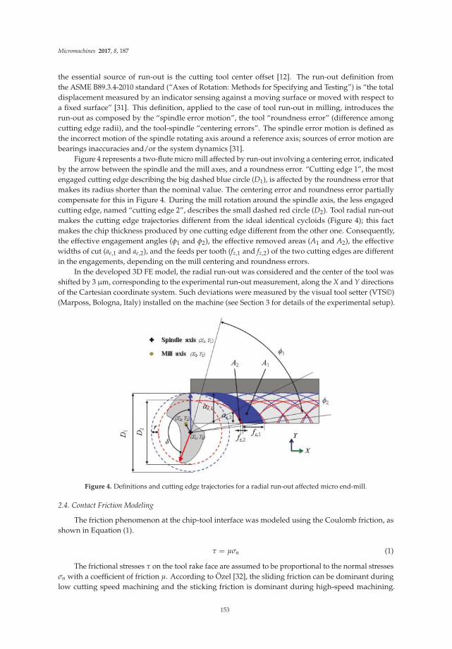
Micromachines 2017, 8, 187
the essential source of run-out is the cutting tool center offset [12]. The run-out definition fromthe ASME B89.3.4-2010 standard (“Axes of Rotation: Methods for Specifying and Testing”) is “the totaldisplacement measured by an indicator sensing against a moving surface or moved with respect toa fixed surface” [31]. This definition, applied to the case of tool run-out in milling, introduces therun-out as composed by the “spindle error motion”, the tool “roundness error” (difference amongcutting edge radii), and the tool-spindle “centering errors”. The spindle error motion is defined asthe incorrect motion of the spindle rotating axis around a reference axis; sources of error motion arebearings inaccuracies and/or the system dynamics [31].
Figure 4 represents a two-flute micro mill affected by run-out involving a centering error, indicatedby the arrow between the spindle and the mill axes, and a roundness error. “Cutting edge 1”, the mostengaged cutting edge describing the big dashed blue circle (D1), is affected by the roundness error thatmakes its radius shorter than the nominal value. The centering error and roundness error partiallycompensate for this in Figure 4. During the mill rotation around the spindle axis, the less engagedcutting edge, named “cutting edge 2”, describes the small dashed red circle (D2). Tool radial run-outmakes the cutting edge trajectories different from the ideal identical cycloids (Figure 4); this factmakes the chip thickness produced by one cutting edge different from the other one. Consequently,the effective engagement angles (φ1 and φ2), the effective removed areas (A1 and A2), the effectivewidths of cut (ae,1 and ae,2), and the feeds per tooth (fz,1 and fz,2) of the two cutting edges are differentin the engagements, depending on the mill centering and roundness errors.
In the developed 3D FE model, the radial run-out was considered and the center of the tool wasshifted by 3 µm, corresponding to the experimental run-out measurement, along the X and Y directionsof the Cartesian coordinate system. Such deviations were measured by the visual tool setter (VTS©)(Marposs, Bologna, Italy) installed on the machine (see Section 3 for details of the experimental setup).
Figure 4. Definitions and cutting edge trajectories for a radial run-out affected micro end-mill.
2.4. Contact Friction Modeling
The friction phenomenon at the chip-tool interface was modeled using the Coulomb friction, asshown in Equation (1).
τ = µσn (1)
The frictional stresses τ on the tool rake face are assumed to be proportional to the normal stressesσn with a coefficient of friction µ. According to Özel [32], the sliding friction can be dominant duringlow cutting speed machining and the sticking friction is dominant during high-speed machining.
153
Micromachines 2017, 8, 187
In micro milling, even if high rotational speeds are used, the cutting speed is lower (in this studyabout 31 m/min) than in macro milling due to the small tool diameter. Consequently, the Coulombsliding friction model can be considered as effective for the micro milling process. The constant valueof the friction coefficient was µ = 0.7 in this study. This value was selected based on the experimentalidentification by Medaska on Al6061-T6 with carbide tools [33]. Al6082-T6 and Al6061-T6 are twopopular aluminum alloys and sometimes they replace each other in the industrial practice due tosimilar characteristics.
2.5. Constitutive Material Model
The reliability of the finite element model results are greatly influenced by the material constitutivelaw and contact conditions at tool-chip and tool-workpiece interfaces [34]. A reliable material modelthat perfectly captures the constitutive behavior of the alloy under high strain, strain rate, andtemperature is critical in machining simulations. A number of different constitutive material modelshave been reported in the literature such as Oxley’s constitutive model [35], the Power law model [26],the strain path dependent model [36], and the Johnson-Cook (JC) model [37], etc. Among the differentconstitutive material models, JC is widely used for machining simulations due to the correspondingmaterial behavior as a function of the strain, strain rate, and temperature [38]. In the present study,the micro end-mill is modelled as a rigid body for the coated carbide tool (TiAlN-X coating with2 µm thickness) with the Advantedge tool default material. However, the workpiece is consideredas viscoplastic material and an essential input is the accurate definition of the workpiece materialproperties and the constitutive material model is represented by the Johnson-Cook model. The flowstress can be expressed as (Equation (2)):
σ =(
A + B (ε)n)[
1 + Cln(
ε·
ε·0
)][
1 − (T − Ta
Tm − Ta)
m]
(2)
where σ is the material flow stress, ε is the plastic strain, ε· is the strain rate, and ε·0 is the referencestrain rate. T is the material temperature, Tm is the melting point, and Ta is the room temperature.The JC constants are as follows: A is the yield stress, B is the pre-exponential factor, C is the strain ratefactor, n is the work hardening exponent, and m is the thermal softening exponent.
Inverse JC Parameters Estimation with 2D FE Simulations
The correct calibration of these parameters is critical to predict the forces, temperature, chipmorphology, etc., with a reasonable accuracy. Unfortunately, there is a lack of standardization for thesecoefficients in the literature. The discrepancies are due to the different methods and test conditionsused for the determination of the material constants [39]. To reduce the uncertainty associated withthe parameters value determination, a viable method based on a machining test was adopted in thispaper. It consists of an inverse method, as used by a number of researchers to obtain the materialconstants [39–41]. In particular, an experimental procedure for identifying the material constants atdifferent cutting conditions was developed. An experimental campaign was specifically carried out.Table 2 shows its cutting conditions and the maximum experimental cutting force measured values.The force measuring system and compensation method applied for this set of experiments and forthe final validation tests are detailed in the experimental procedure (Section 3). Each experiment wasreplicated two times to consider the experimental variability. Four parameters of the Johnson-Cookequation (A, B, n, C), which were the most susceptible to the strain hardening effect, were selected.
The simulations plan was based on a 24 full factorial design (two levels and 4 factors, Table 3).16 JC parameter combinations were used for simulating each cutting condition of Table 2, for a totalof 64 runs. An initial JC parameters combination for the 6082-T6 aluminum alloy was taken from(Table 3). These values were obtained at high strain rates by conducting split Hopkinson pressurebar (SHPB) tests in conditions similar to metal cutting. The other level was obtained by scaling downthe [42] values by 50%, apart from the m one (Table 3). This scale was applied due to the overestimated
154

Micromachines 2017, 8, 187
result of the cutting force simulations with original values [27]. Other physical properties of Al6082-T6used in the FE model are presented in Table 4 [43].
Table 2. Experimental and 2D simulated cutting conditions.
CuttingConditions
ToolDiameter
CuttingSpeed
Radial Depthof Cut (ae)
Axial Depthof Cut (ap)
Feed Per Tooth Fx Fy
(mm) (m/min) (mm) (mm) (µm/(Tooth·Rev)) (N) (N)
1 0.5 28 0.125 0.05 4 0.7 0.32 0.5 28 0.25 0.05 4 0.93 0.83 0.5 28 0.125 0.1 4 1.3 0.644 0.5 28 0.25 0.1 4 1.63 1.2
Table 3. Johnson-Cook constants for Al6082-T6.
Level A (MPa) B (MPa) C m n
1 428.5 327.7 0.00747 1.31 1.008 [39]2 214.25 163.85 0.003735 1.31 0.504
The FEM simulations in the inverse method were carried out to evaluate the best combination ofJC parameters for obtaining the most accurate cutting forces. A simplified 2D FE model was used toreduce the computational effort to carry out the total 64 simulations, under the hypothesis that thebest JC parameters would also perform well in the 3D case.
Figure 5 shows the setup and the general geometry of the 2D micro end-milling FEM simulation.The workpiece bottom boundary nodes are fixed in the Y direction and the tool in both the X and Y
directions. The workpiece moves with a cutting speed or surface velocity, while the tool is stationary.The axial depth of cut is measured in the Z direction, perpendicular to the feed and speed directions.The rigid cutting tool was meshed using 670 brick elements. The workpiece was meshed with six-nodequadratic triangular elements for a total number of 1566 nodes. The maximum and minimum elementsizes for the workpiece were set to 0.1 mm and 0.002 mm, respectively. The maximum element size ofthe cutter was set at 0.2 mm and the minimum at 0.002 mm. The friction phenomenon at the chip-toolinterface was the same as in the 3D FE model, with the same coefficient of friction. A large value of theinterface heat transfer coefficient hint = 104 (N/s mm ◦C) was selected for these simulations to ensurethat they reached a steady state condition.
Figure 5. Setup and boundary conditions of the 2D micro end-milling FEM.
155

Micromachines 2017, 8, 187
After running the 2D simulations for all the designed parameter combinations, the maximumforces were extracted from the simulations. The errors between the predicted and the experimentalforce components (Fx and Fy) were calculated and recorded for all tested combinations. The total errorwas calculated by (Equation (3)). Each relative error was squared in this equation. Squares were foundand summed for each force component and each cutting condition. Subsequently, the sum of thesquare was divided by M × N (M: number of cutting conditions (4); N: number of force components(2)). The square root of this value gives the forces total error, representing the performance of eachflow stress model representation. Table 5 shows the total errors for the 16 JC parameter combinations.In the case of the second parameters combination, an error occurred in the simulations preventing usfrom obtaining results in all cutting conditions.
For these sets of parameters, it was observed that the resultant total error varied between 15.73and 73.06%. According to these results, the best set of parameters was selected to represent the materialflow stress in the following 3D simulations, as presented in Table 6.
Errortotal =
√
√
√
√
∑Mj=1 ∑
Ni=1[(
Fji,Ex−Fji,Sim
Fji,Ex)2]
N × M(3)
Table 4. Material properties for Al6082-T6 [43].
Property Unit Value
Young’s modulus, E (GPa) 70Poisson ratio, v - 0.33
Density, ρ (g/cm2) 2.70Thermal conductivity, K (W/m·K) 180
Specific heat, Cp (J/Kg·◦C) 700Thermal expansion coefficient - 24 × 10−6
Melting temperature, Tmelt (◦C) 582
Table 5. Simulated force results and comparison with experiments.
NoCoded Variable Cutting Conditions
A B n C 1 2 3 4
Fx Fy Fx Fy Fx Fy Fx Fy Total Error
(MPa) (MPa) (N) (N) (N) (N) (N) (N) (N) (N) (%)
1 428.5 327.7 1.008 0.003735 1.4 0.33 1.77 0.4 2.4 0.7 3.2 0.82 65.562 214.25 163.85 0.504 0.00747 0.06 0.04 0.06 0.04 0.1 0.14 0.09 0.13 Error3 214.25 327.7 1.008 0.003735 0.3 0.15 1.4 0.3 0.6 0.3 2.7 0.5 57.814 214.25 327.7 1.008 0.00747 1 0.24 1.2 0.58 0.83 0.42 2.1 0.75 31.135 428.5 327.7 1.008 0.00747 1.3 0.32 1.7 0.4 2.6 0.7 3.8 0.8 73.066 428.5 327.7 0.504 0.003735 0.82 0.43 1.1 0.57 1.7 0.88 2.4 1.1 24.77 428.5 163.85 0.504 0.00747 0.54 0.35 0.72 0.65 1.1 0.6 0.83 0.61 30.888 428.5 163.85 0.504 0.003735 0.55 0.24 0.86 0.38 0.98 0.65 1.5 0.8 28.389 428.5 163.85 1.008 0.00747 0.97 0.33 1.33 0.4 1.95 0.7 2.6 0.8 39.7110 214.25 163.85 1.008 0.003735 0.65 0.16 0.08 0.14 1.4 0.3 0.45 0.2 64.2411 214.25 163.85 1.008 0.00747 0.82 0.21 0.17 0.09 1.5 0.35 0.35 0.18 62.5712 214.25 327.7 0.504 0.00747 0.83 0.3 0.98 0.56 1.48 0.63 1.78 0.89 15.7313 214.25 163.85 0.504 0.003735 0.54 0.24 0.7 0.3 1.03 0.46 1.4 0.6 35.9314 428.5 327.7 0.504 0.00747 1 0.47 1.4 0.6 2 1 2.75 1.2 47.6815 428.5 163.85 1.008 0.003735 0.3 0.19 1.23 0.34 1.9 0.65 2.5 0.73 45.5116 214.25 327.7 0.504 0.003735 0.85 0.27 0.65 0.54 1.6 0.53 0.92 0.83 27.87
Error: with the following material combination constants simulations did not finished to the end.
156

Micromachines 2017, 8, 187
Table 6. Best set of JC Al6082-T6 flow stress model constants used for 3D simulations.
A (MPa) B (MPa) C m n Tm (◦C) Ta (◦C)
214.25 327.7 0.00747 1.31 0.504 582 21
3. FEM Validation Experimental Procedure
In order to verify the accuracy of the developed numerical model, both the predicted cuttingforces and temperatures were validated against experiments. The machine tool is one of the criticalaspects of micro machining in order to achieve a high precision on machined components and have astable machining process [44]. Micro milling operations have been performed on a Kern EVO ultraprecision 5-axis machining center (nominal positioning tolerance = ±1 µm, precision on the workpiece= ±2 µm). The machine tool and experimental setup are illustrated in Figure 6a.
The cutting tool tips were inspected and measured prior to machining and the only tools withminimal geometrical inaccuracies and defects were selected for the experiments. The run-out ofmicro end-mills was measured with both static (Figure 6c) and dynamic (Figure 6b) methods. In thestatic run-out measurements, a dial gauge was used by placing its probe against the tool shank,manually rotating the spindle, and reading the value of run-out as the “total indicator reading” [31].The measured run-out was 3 ± 1 µm for both tool measurements. The micro mill dynamic run-out wasmeasured by a visual tool setter VTS (Marposs, Bologna, Italy), is equipped with a camera synchronizedwith the spindle rotation to acquire a set of tool diascopic images at a defined angular step. A dedicatedsoftware analyzes these images and calculates the tool diameter, the maximum tool dynamic diameter(or flying circle diameter) D1, and the radial runout (or TIR) r [31], corresponding to the differencebetween the maximum and the minimum tool dynamic radii. The minimum tool dynamic diameter D2
can be obtained from D1 and r (Figure 4). The experimental setup is shown in Figure 6b. The dynamicmeasurement was performed at the same rotational speed of the final experiments after the requiredVTS speed calibration. The tool radial run-out with respect to the spindle axis was 4 ± 0.5 µm and thisvalue was used in the simulations. The measurements were repeated five times in order to guaranteestatistical consistency. The standard deviation of the measurement was XYZ µm, equivalent to XY%of the measured run-out. Micro end-mills were held in HSK32 Kern/Schaublin tool holders anda precision Schaublin collet (type D14, 74-14000) was used to reduce the clamping error and thetool run-out.
Full slot micro end-milling was carried out in dry cutting conditions. The cutting parameters aresummarized in Table 7. The cutting conditions were selected according to the literature [45,46], tryingto avoid significant rubbing and burr formation due to the feeds per tooth below the cutting edgeradius. Four replicates were performed for each cutting condition to consider experimental variability.
Table 7. Experimental tests conditions.
Cutting Parameters Symbol Test1 Test2
Axial depth of cut (mm) ap 0.05 0.05Radial depth of cut (mm) ae 0.5 0.5
Feed per tooth (µm/(tooth·rev)) fz 8 4Cutting speed (m/min) vc 31.4 31.4
Spindle speed (rpm) n 20,000 20,000
Approach Full slot
157
Micromachines 2017, 8, 187
Figure 6. (a) Machine tool and experimental setup; (b) dynamic run-out measurement; (c) staticrun-out measurement; (d) schematic of experimental temperature measurement setup; (e) temperaturedistribution in end-mill; (f) dynamometer and force compensation.
3.1. Force Measurement
The cylindrical workpiece (Figure 6f) was fixed on a Kistler 9317B miniature piezoelectricthree-axial dynamometer (Figure 6f), which measured the obtained cutting force signals (measuringrange: Fx, Fy = ±1000 N, Fz = ±2000 N; linearity error ≤ 0.5% FSO, Full Scale Output) amplifiedby three Kistler 5015A charge amplifiers. A low-pass filter at 20,000 Hz was directly appliedon the charge amplifiers in order to avoid aliasing and a Hanning window was used to reduceleakage. The acquisition time window was one second long for each milling step. The cutting forcemeasurements were affected by vibrations due to the low resonance frequency of the fixturing andforce measurement system. In order to accurately measure the micro milling forces, a compensationmethod was applied to the measured forces [47]. The dynamometer dynamic behavior was identifiedfrom the impact tests applied in both the X and Y directions on the same workpiece material (Figure 6f).Figure 7 shows the result of the impact test used to obtain the frequency response function of thedynamometer in both directions. The same experimental setup and procedure was used for the inversemethod experiments for determining the JC parameters (Section “Inverse JC Parameters Estimationwith 2D FE Simulations”).
158

Micromachines 2017, 8, 187
Figure 7. FRFs of the dynamometer in (a) X and (b) Y directions.
3.2. Infrared Temperature Measurements
The infrared ThermaCAMTM SC 3000 Researcher camera (FLIR Systems, Boston, MA, USA) witha waveband in the electromagnetic spectrum (in the range of 8–9 µm) was used for measuringthe temperature at the cutting area. The measurement accuracy of the camera was ±1% or±1 ◦C (for measurement ranges up to +150 ◦C) with a spatial resolution (IFOV) of 1.1 mrad.Crisp high-resolution 14-bit images and thermal data were captured and stored at high rates (upto 900 Hz) on high capacity PC. The camera was positioned along the cutting direction (Figure 6d).The temperature measurement was carried out at the tool tip area, as shown in Figure 6e. An infraredcamera was calibrated with a set of standard blackbodies at various temperatures. The lenses havetheir own unique calibration to insure accuracy and the camera will automatically identify the lensattachment and load appropriate data in the radiometric calculations. The emissivity and backgroundcorrection are variable, from 0.01 to 1.0 [48]. The camera microscope lens was used to acquire imagesat a 75–99 mm focus range, adjusted on the micro tool with a ±0.05 mm depth of focus. All of theexperimental data have been normalized to a room temperature of 21 ◦C.
159
Micromachines 2017, 8, 187
4. Results and Discussion
4.1. Chip Formation
The micro milling full slot operation was simulated for both types of teeth engagements.The calculation time was in the range of 30 ± 3 h, depending on the cutting condition. The differentresults obtained at the end of the simulations for each cutting condition are presented in this section.Figure 8 shows the chip formation and plastic strain distribution during the micro milling process intwo cutting conditions, Test1 (fz = 8 µm/(tooth·rev)) and Test2 (fz = 4 µm/(tooth·rev)), for differentangular positions of both cutting teeth. The maximum plastic strain occurred in the chip area, mainlynear to the end of the cut (about 50 micros from tool tip). As expected, the plastic strain is greaterwhen the feed is higher. The feed effect on the chip formation is also clear since different chip volumescan be observed at the same angular position. Figure 9 shows the chips at the end of the cut (θ = 360◦).The effects of the tool run-out on the chip shape are visible in Figures 9 and 10. Due to the unequalload, the first and second removed chips present different shapes and sizes.
Figure 8. 3D chip formation prediction and plastic strain distribution at different angular positions(a) Test1 and (b) Test2.
160
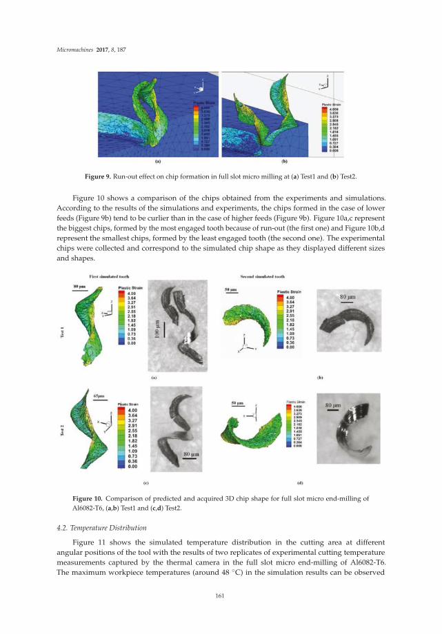
Micromachines 2017, 8, 187
Figure 9. Run-out effect on chip formation in full slot micro milling at (a) Test1 and (b) Test2.
Figure 10 shows a comparison of the chips obtained from the experiments and simulations.According to the results of the simulations and experiments, the chips formed in the case of lowerfeeds (Figure 9b) tend to be curlier than in the case of higher feeds (Figure 9b). Figure 10a,c representthe biggest chips, formed by the most engaged tooth because of run-out (the first one) and Figure 10b,drepresent the smallest chips, formed by the least engaged tooth (the second one). The experimentalchips were collected and correspond to the simulated chip shape as they displayed different sizesand shapes.
Figure 10. Comparison of predicted and acquired 3D chip shape for full slot micro end-milling ofAl6082-T6, (a,b) Test1 and (c,d) Test2.
4.2. Temperature Distribution
Figure 11 shows the simulated temperature distribution in the cutting area at differentangular positions of the tool with the results of two replicates of experimental cutting temperaturemeasurements captured by the thermal camera in the full slot micro end-milling of Al6082-T6.The maximum workpiece temperatures (around 48 ◦C) in the simulation results can be observed
161
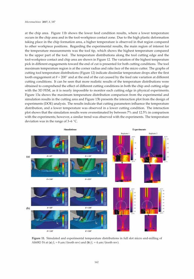
Micromachines 2017, 8, 187
at the chip area. Figure 11b shows the lower feed condition results, where a lower temperatureoccurs in the chip area and in the tool-workpiece contact zone. Due to the high plastic deformationtaking place in the chip formation area, a higher temperature is observed in that region comparedto other workpiece positions. Regarding the experimental results, the main region of interest forthe temperature measurements was the tool tip, which shows the highest temperature comparedto the upper part of the tool. The temperature distributions along the tool cutting edge and thetool-workpiece contact and chip area are shown in Figure 12. The variation of the highest temperaturepick in different engagements toward the end of cut is presented for both cutting conditions. The toolmaximum temperature region is at the corner radius and rake face of the micro cutter. The graphs ofcutting tool temperature distributions (Figure 12) indicate dissimilar temperature drops after the firsttooth engagement at θ = 200◦ and at the end of the cut caused by the feed rate variation at differentcutting conditions. It can be seen that more realistic results of the temperature distributions wereobtained to comprehend the effect of different cutting conditions in both the chip and cutting edgewith the 3D FEM, as it is nearly impossible to monitor each cutting edge in physical experiments.Figure 13a shows the maximum temperature distribution comparison from the experimental andsimulation results in the cutting area and Figure 13b presents the interaction plot from the design ofexperiments (DOE) analysis. The results indicate that cutting parameters influence the temperaturedistribution, and a lower temperature was observed in a lower cutting condition. The interactionplot shows that the simulation results were overestimated by between 7% and 12.5% in comparisonwith the experiments; however, a similar trend was observed with the experiments. The temperaturedeviation was in the range of 3–6 ◦C.
Figure 11. Simulated and experimental temperature distributions in full slot micro end-milling ofAl6082-T6 at (a) fz = 8 µm/(tooth·rev) and (b) fz = 4 µm/(tooth·rev).
162

Micromachines 2017, 8, 187
Figure 12. Simulated temperature distribution along the cutting edge for (a) Test1 and (b) Test2.
Figure 13. (a) Comparison of experimental and simulated maximum temperature distribution and (b)interaction plot of temperature distribution
4.3. Cutting Forces Predictions
It was noted that all the simulated forces were affected by a relevant amount of numericalnoise distributed at an extremely high frequency range, much beyond the range of real cutting forcecontributions. A fifth-order Butterworth low-pass filter was therefore applied to the simulated signalswith a cut-off frequency equal to the bandwidth achievable by the dynamometer installed on themachine, which is around 4000 Hz (after the application of the acquired force compensation [41]),in order to obtain simulated force signals comparable with the experiments. The comparisons wereperformed between results obtained by the finite element model and the physical experiments.Figure 14 shows the cutting force components Fx, Fy, and Fz obtained for both teeth engagements,considering the effect of the run-out in the full slot micro end-milling process. The comparison betweenthe experiments and simulation reveals globally similar trends for Fx, and Fy components in terms ofthe curve shapes. However, some discrepancies in the magnitude of forces were observed, probablydue to aluminum particles sticking to the tool (build up edge) that affect the tool geometry and the tooldynamics. The effect of the run-out phenomenon is visible in the cutting force results as the first tooth
163
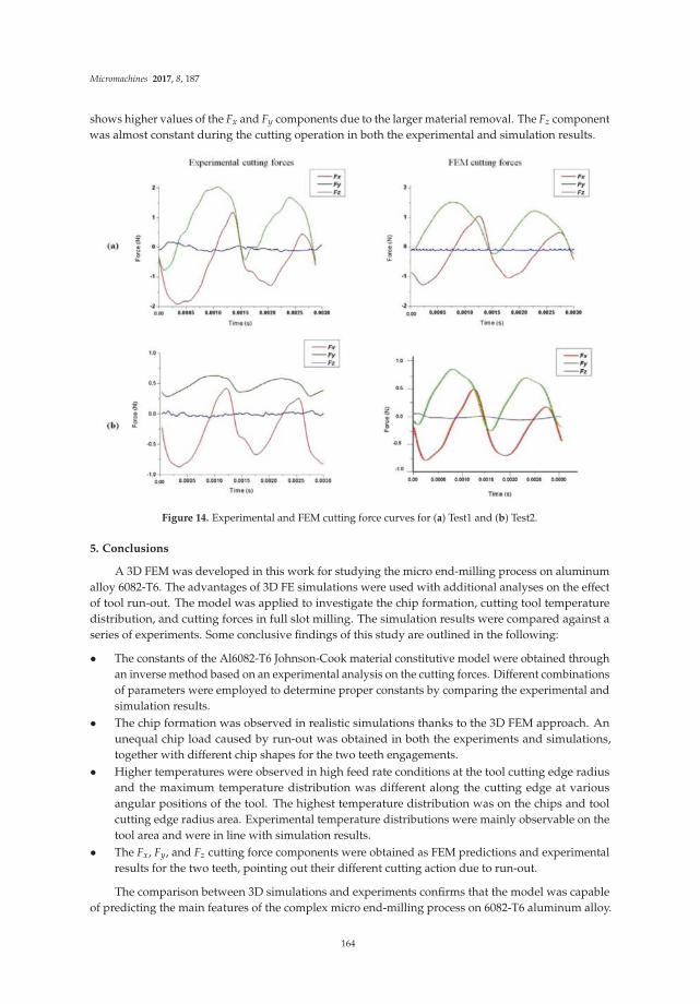
Micromachines 2017, 8, 187
shows higher values of the Fx and Fy components due to the larger material removal. The Fz componentwas almost constant during the cutting operation in both the experimental and simulation results.
Figure 14. Experimental and FEM cutting force curves for (a) Test1 and (b) Test2.
5. Conclusions
A 3D FEM was developed in this work for studying the micro end-milling process on aluminumalloy 6082-T6. The advantages of 3D FE simulations were used with additional analyses on the effectof tool run-out. The model was applied to investigate the chip formation, cutting tool temperaturedistribution, and cutting forces in full slot milling. The simulation results were compared against aseries of experiments. Some conclusive findings of this study are outlined in the following:
• The constants of the Al6082-T6 Johnson-Cook material constitutive model were obtained throughan inverse method based on an experimental analysis on the cutting forces. Different combinationsof parameters were employed to determine proper constants by comparing the experimental andsimulation results.
• The chip formation was observed in realistic simulations thanks to the 3D FEM approach. Anunequal chip load caused by run-out was obtained in both the experiments and simulations,together with different chip shapes for the two teeth engagements.
• Higher temperatures were observed in high feed rate conditions at the tool cutting edge radiusand the maximum temperature distribution was different along the cutting edge at variousangular positions of the tool. The highest temperature distribution was on the chips and toolcutting edge radius area. Experimental temperature distributions were mainly observable on thetool area and were in line with simulation results.
• The Fx, Fy, and Fz cutting force components were obtained as FEM predictions and experimentalresults for the two teeth, pointing out their different cutting action due to run-out.
The comparison between 3D simulations and experiments confirms that the model was capableof predicting the main features of the complex micro end-milling process on 6082-T6 aluminum alloy.
164

Micromachines 2017, 8, 187
Acknowledgments: The research leading to these results has received funding from the People Programme(Marie Curie Actions) of the European Union’s Seventh Framework Programme (FP7/2007-2013) under REA grantagreement No. 609405 (COFUNDPostdocDTU). The authors would also like to acknowledge the Politecnico diMilano University for founding the PhD project “3D Finite Element Modeling of Micro End-Milling by ConsideringTool Run-Out, Temperature Distribution, Chip and Burr Formation” by A.D. This research work was undertakenin the context of MICROMAN project (“Process Fingerprint for Zero-defect Net-shape MICROMANufacturing”,http://www.microman.mek.dtu.dk/). MICROMAN is a European Training Network supported by Horizon 2020,the EU Framework Programme for Research and Innovation (Project ID: 674801).
Author Contributions: Ali Davoudinejad carried out simulations, experiments, measurements and wrote thepaper; Guido Tosello, Paolo Parenti and Massimiliano Annoni revised the paper.
Conflicts of Interest: The authors declare no conflict of interest.
References
1. Uriarte, L.; Herrero, A.; Lvanov, A.; Oosterling, H.; Staemmler, L.; Tang, P.T.; Allen, D. Comparison between
microfabrication technologies for metal tooling. Proc. Inst. Mech. Eng. Part C J. Mech. Eng. Sci. 2006, 220,
1665–1676. [CrossRef]
2. DeVor, R.E.; Ehmann, K.F.; Kapoor, S.G. Technology Assessment on Current Advanced Research in
Micro-Machining and Related Areas; The Association For Manufacturing Technology: McLean, VA, USA,
2004; p. 239.
3. Dornfeld, D.; Min, S.; Takeuchi, Y. Recent advances in mechanical micromachining. CIRP Ann. Manuf. Technol.
2006, 55, 745–768. [CrossRef]
4. Anand, R.S.; Patra, K. Modeling and simulation of mechanical micro-machining—A review.
Mach. Sci. Technol. 2014, 18, 323–347. [CrossRef]
5. Koo, J.-Y.; Kim, J.-S.; Kim, P.-H. Machining Characteristics of Micro-Flow Channels in Micro-Milling Process.
Mach. Sci. Technol. 2014, 18, 509–521. [CrossRef]
6. Bao, W.Y.; Tansel, I.N. Modeling micro-end-milling operations. Part II: Tool run-out. Int. J. Mach. Tools Manuf.
2000, 40, 2175–2192. [CrossRef]
7. Dhanorker, A.; Özel, T. An Experimental and Modeling Study on Meso/Micro End Milling Process.
In Proceedings of the ASME 2006 International Manufacturing Science and Engineering Conference, Ypsilanti,
MI, USA, 8–11 October 2006; pp. 1071–1079.
8. Ma, J.; Duong, N.H.; Lei, S. Finite element investigation of friction and wear of microgrooved cutting tool in
dry machining of AISI 1045 steel. Proc. Inst. Mech. Eng. Part J J. Eng. Tribol. 2014, 229, 449–464. [CrossRef]
9. Liu, K.; Melkote, S.N. Finite element analysis of the influence of tool edge radius on size effect in orthogonal
micro-cutting process. Int. J. Mech. Sci. 2007, 49, 650–660. [CrossRef]
10. Liu, K.; Melkote, S.N. Material strengthening mechanisms and their contribution to size effect in
micro-cutting. J. Manuf. Sci. Eng. 2005, 128, 730–738. [CrossRef]
11. Ucun, I.; Aslantas, K.; Bedir, F. Finite element modeling of micro-milling: Numerical simulation and
experimental validation. Mach. Sci. Technol. 2016, 20, 148–172. [CrossRef]
12. Afazov, S.M.; Ratchev, S.M.; Segal, J. Modelling and simulation of micro-milling cutting forces. J. Mater.
Process. Technol. 2010, 210, 2154–2162. [CrossRef]
13. Jin, X.; Altintas, Y. Prediction of micro-milling forces with finite element method. J. Mater. Process. Technol.
2012, 212, 542–552. [CrossRef]
14. Thepsonthi, T.; Özel, T. Experimental and finite element simulation based investigations on micro-milling
Ti-6Al-4V titanium alloy: Effects of cBN coating on tool wear. J. Mater. Process. Technol. 2013, 213, 532–542.
[CrossRef]
15. Pratap, T.; Patra, K.; Dyakonov, A.A. Modeling cutting force in micro-milling of Ti-6Al-4V titanium alloy.
Procedia Eng. 2015, 129, 134–139. [CrossRef]
16. Bajpai, V.; Lee, I.; Park, H.W. Finite element modeling of three-dimensional milling process of Ti-6Al-4V.
Mater. Manuf. Process. 2014, 29, 564–571. [CrossRef]
17. Wu, H.B.; Zhang, S.J. 3D FEM simulation of milling process for titanium alloy Ti6Al4V. Int. J. Adv.
Manuf. Technol. 2014, 71, 1319–1326. [CrossRef]
18. Min, S.; Dornfeld, D.A.; Kim, J.; Shyu, B. Finite element modeling of burr formation in metal cutting.
Mach. Sci. Technol. 2001, 5, 307–322. [CrossRef]
165

Micromachines 2017, 8, 187
19. Yang, K.; Liang, Y.; Zheng, K.; Bai, Q.; Chen, W. Tool edge radius effect on cutting temperature in
micro-end-milling process. Int. J. Adv. Manuf. Technol. 2011, 52, 905–912. [CrossRef]
20. Mamedov, A.; Lazoglu, I. Thermal analysis of micro milling titanium alloy Ti-6Al-4V. J. Mater. Process. Technol.
2016, 229, 659–667. [CrossRef]
21. Wang, F.; Zhao, J.; Li, A.; Zhu, N.; Zhao, J. Three-dimensional finite element modeling of high-speed end
milling operations of Ti-6Al-4V. Proc. Inst. Mech. Eng. Part B J. Eng. Manuf. 2014, 228, 893–902. [CrossRef]
22. Davoudinejad, A.; Parenti, P.; Annoni, M. 3D finite element prediction of chip flow, burr formation, and
cutting forces in micro end-milling of aluminum 6061-T6. Front. Mech. Eng. 2017, 1–12. [CrossRef]
23. Thepsonthi, T.; Özel, T. 3-D finite element process simulation of micro-end milling Ti-6Al-4V titanium alloy:
Experimental validations on chip flow and tool wear. J. Mater. Process. Technol. 2015, 221, 128–145. [CrossRef]
24. Ulutan, D.; Lazoglu, I.; Dinc, C. Three-dimensional temperature predictions in machining processes using
finite difference method. J. Mater. Process. Technol. 2009, 209, 1111–1121. [CrossRef]
25. Bil, H.; Kılıç, S.E.; Tekkaya, A.E. A comparison of orthogonal cutting data from experiments with three
different finite element models. Int. J. Mach. Tools Manuf. 2004, 44, 933–944. [CrossRef]
26. Man, X.; Ren, D.; Usui, S.; Johnson, C.; Marusich, T.D. Validation of finite element cutting force prediction
for end milling. Procedia CIRP 2012, 1, 663–668. [CrossRef]
27. Davoudinejad, A. 3D Finite Element Modeling of Micro End-Milling by Considering Tool Run-Out, Temperature
Distribution, Chip and Burr Formation; University of Politecnico di Milano: Milan, Italy, 2016.
28. Rebaioli, L.; Annoni, M.; Davoudinejad, A.; Parenti, P. Performance of Micro End Milling Force Prediction
on Aluminum 6061-T6 with 3D FE Simulation. In Proceedings of the 4M/ICOMM 2015-International
Conference on Micromanufacturing, Milan, Italy, 31 March–2 April 2015.
29. Davoudinejad, A.; Chiappini, E.; Tirelli, S.; Annoni, M.; Strano, M. Finite Element Simulation and Validation
of Chip Formation and Cutting Forces in Dry and Cryogenic Cutting of Ti-6Al-4V. Procedia Manuf. 2015, 1,
728–739. [CrossRef]
30. Niesłony, P.; Grzesik, W.; Chudy, R.; Habrat, W. Meshing strategies in FEM simulation of the machining
process. Arch. Civ. Mech. Eng. 2015, 15, 62–70. [CrossRef]
31. American National Standards Institute (ASME). Axes of Rotation: Methods for Specifying and Testing; American
Society of Mechanical Engineers: New York, NY, USA, 1986.
32. Özel, T. The influence of friction models on finite element simulations of machining. Int. J. Mach. Tools Manuf.
2006, 46, 518–530. [CrossRef]
33. Medaska, M.K.; Nowag, L.; Liang, S.Y. Simultaneous measurement of the thermal and tribological effects of
cutting fluid. Mach. Sci. Technol. 1999, 3, 221–237. [CrossRef]
34. Umbrello, D.; M’Saoubi, R.; Outeiro, J.C. The influence of Johnson-Cook material constants on finite element
simulation of machining of AISI 316L steel. Int. J. Mach. Tools Manuf. 2007, 47, 462–470. [CrossRef]
35. Oxley, P.L.B. The Mechanics of Machining: An Analytical Approach to Assessing Machinability; E. Horwood:
Chichester, UK, 1989.
36. Katsuhiro, M.; Takahiro, S.; Eiji, U. Flow stress of low carbon steel at high temperature and strain rate. II:
Flow stress under variable temperature and variable strain rate. Bull. Jpn. Soc. Precis. Eng. 1983, 17, 167–172.
37. Johnson, G.R.; Cook, W.H. A constitutive Model and Data for Metals Subjected to Large Strains, High Strain
Rates and High Temperatures. In Proceedings of the 7th International Symposium on Ballistics, Hague,
The Netherlands, 19–21 April 1983; pp. 541–547.
38. Dixit, U.S.; Joshi, S.N.; Davim, J.P. Incorporation of material behavior in modeling of metal forming and
machining processes: A review. Mater. Des. 2011, 32, 3655–3670. [CrossRef]
39. Daoud, M.; Jomaa, W.; Chatelain, J.F.; Bouzid, A. A machining-based methodology to identify material
constitutive law for finite element simulation. Int. J. Adv. Manuf. Technol. 2015, 77, 2019–2033. [CrossRef]
40. Guo, Y.B. An integral method to determine the mechanical behavior of materials in metal cutting. J. Mater.
Process. Technol. 2003, 142, 72–81. [CrossRef]
41. Özel, T.; Zeren, E. A Methodology to determine work material flow stress and tool-chip interfacial friction
properties by using analysis of machining. J. Manuf. Sci. Eng. 2005, 128, 119–129. [CrossRef]
42. Jaspers, S.P.F.; Dautzenberg, J. Material behaviour in conditions similar to metal cutting: Flow stress in the
primary shear zone. J. Mater. Process. Technol. 2002, 122, 322–330. [CrossRef]
43. Aalco metals Ltd. Aluminium Alloy 6082-T6~T651 Plate; Aalco Metals Ltd.: Cobham, UK, 2013; pp. 24–25.
166

Micromachines 2017, 8, 187
44. Lamikiz, A.; de Lacalle, L.N.; Celaya, A. Machine Tool Performance and Precision. In Machine Tools for High
Performance Machining; de Lacalle, L.N., Lamikiz, A., Eds.; Springer: London, UK, 2009; pp. 219–260.
45. Gillespie, L.K.; Blotter, P.T. The Formation and Properties of Machining Burrs. J. Eng. Ind. 1976, 98, 66.
[CrossRef]
46. Mathai, G.K.; Melkote, S.N.; Rosen, D.W. Effect of process parameters on burrs produced in micromilling of
a thin nitinol foil. J. Micro Nano Manuf. 2013, 1, 21005–21010. [CrossRef]
47. Annoni, M.; Pusterla, N.; Rebaioli, L.; Semeraro, Q. Calibration and validation of a mechanistic micromilling
force prediction model. J. Manuf. Sci. Eng. 2015, 138, 11001–11012. [CrossRef]
48. ThermCAM® Researcher Features/Specifications; FLIR Systems: Boston, MA, USA, 2002.
© 2017 by the authors. Licensee MDPI, Basel, Switzerland. This article is an open access
article distributed under the terms and conditions of the Creative Commons Attribution
(CC BY) license (http://creativecommons.org/licenses/by/4.0/).
167
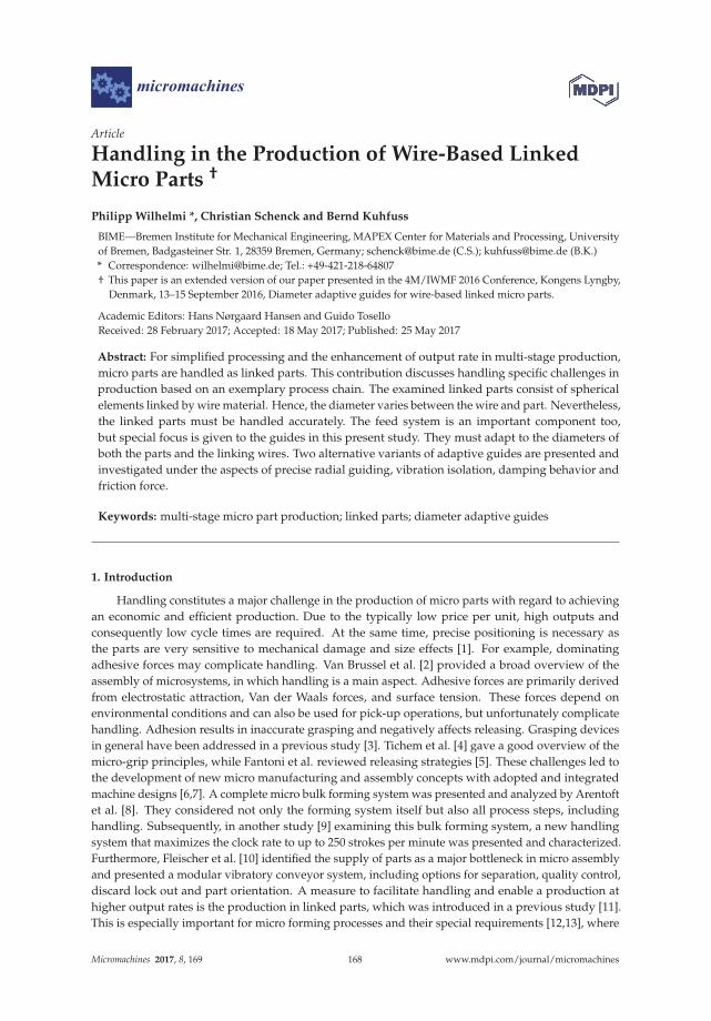
micromachines
Article
Handling in the Production of Wire-Based LinkedMicro Parts †
Philipp Wilhelmi *, Christian Schenck and Bernd Kuhfuss
BIME—Bremen Institute for Mechanical Engineering, MAPEX Center for Materials and Processing, Universityof Bremen, Badgasteiner Str. 1, 28359 Bremen, Germany; [email protected] (C.S.); [email protected] (B.K.)* Correspondence: [email protected]; Tel.: +49-421-218-64807† This paper is an extended version of our paper presented in the 4M/IWMF 2016 Conference, Kongens Lyngby,
Denmark, 13–15 September 2016, Diameter adaptive guides for wire-based linked micro parts.
Academic Editors: Hans Nørgaard Hansen and Guido ToselloReceived: 28 February 2017; Accepted: 18 May 2017; Published: 25 May 2017
Abstract: For simplified processing and the enhancement of output rate in multi-stage production,micro parts are handled as linked parts. This contribution discusses handling specific challenges inproduction based on an exemplary process chain. The examined linked parts consist of sphericalelements linked by wire material. Hence, the diameter varies between the wire and part. Nevertheless,the linked parts must be handled accurately. The feed system is an important component too,but special focus is given to the guides in this present study. They must adapt to the diameters ofboth the parts and the linking wires. Two alternative variants of adaptive guides are presented andinvestigated under the aspects of precise radial guiding, vibration isolation, damping behavior andfriction force.
Keywords: multi-stage micro part production; linked parts; diameter adaptive guides
1. Introduction
Handling constitutes a major challenge in the production of micro parts with regard to achievingan economic and efficient production. Due to the typically low price per unit, high outputs andconsequently low cycle times are required. At the same time, precise positioning is necessary asthe parts are very sensitive to mechanical damage and size effects [1]. For example, dominatingadhesive forces may complicate handling. Van Brussel et al. [2] provided a broad overview of theassembly of microsystems, in which handling is a main aspect. Adhesive forces are primarily derivedfrom electrostatic attraction, Van der Waals forces, and surface tension. These forces depend onenvironmental conditions and can also be used for pick-up operations, but unfortunately complicatehandling. Adhesion results in inaccurate grasping and negatively affects releasing. Grasping devicesin general have been addressed in a previous study [3]. Tichem et al. [4] gave a good overview of themicro-grip principles, while Fantoni et al. reviewed releasing strategies [5]. These challenges led tothe development of new micro manufacturing and assembly concepts with adopted and integratedmachine designs [6,7]. A complete micro bulk forming system was presented and analyzed by Arentoftet al. [8]. They considered not only the forming system itself but also all process steps, includinghandling. Subsequently, in another study [9] examining this bulk forming system, a new handlingsystem that maximizes the clock rate to up to 250 strokes per minute was presented and characterized.Furthermore, Fleischer et al. [10] identified the supply of parts as a major bottleneck in micro assemblyand presented a modular vibratory conveyor system, including options for separation, quality control,discard lock out and part orientation. A measure to facilitate handling and enable a production athigher output rates is the production in linked parts, which was introduced in a previous study [11].This is especially important for micro forming processes and their special requirements [12,13], where
Micromachines 2017, 8, 169 168 www.mdpi.com/journal/micromachines

Micromachines 2017, 8, 169
multiple different operations may be performed on a single part. Applications of this approach tobulk forming based on sheet metal have been presented previously in the literature [14,15]. In contrast,the work presented in this paper addresses bulk forming based on wire material. Figure 1 showsan example of the production of wire-based linked micro parts. In the first process, preforms aregenerated within a wire by a laser material accumulation process [16]. The wire is melted partiallywhile being pushed together. The remaining sections of the wire build the frame structure that linksup the preforms. In a second step, the preforms are formed by micro rotary swaging [17,18].
Figure 1. Example of wire-based linked micro part production.
To enable the production of linked parts at high output rates, appropriate production facilities aredeveloped and investigated. The feed system is essential for the accumulation process. It must providea high dynamic positioning with adequate precision and accurate alignment of the wire within theprocess zone. The chosen solution in this case is a gripper-based feed system driven by a linear directdrive. The grippers are self-centering and aligned to each other by the design concept. The grippergeometry provides good support of the wire by line contact. Nevertheless, the distance of the preformswithin the linked parts may vary due to changes in length of the frame structure during a multi-stageproduction process, especially when forming is included [18]. Hence, a referencing of the individualparts becomes necessary for the positioning in a subsequent production process. Therefore, a visualhigh-speed part referencing system has been developed [19]. The system is based on a line camera,which is triggered based on the signal of the position sensor of the feed system. Appropriate guidesare important to guide the linked parts securely through the process chain, and such guides are alsoaddressed in this paper.
2. Requirements for Adaptive Guides
Depending on the processes and their spatial alignment, the guides along the process chain mustmeet different requirements. It is important that the guides suppress vibrations that occur betweenthese processes. The part must be centered within the tools, close to the process. The vibrationsinduced by the process should be damped and the transmission of vibrations from the process to thelinked parts outside the tool and vice versa must be suppressed. Furthermore, a compact size canbe important due to space limitations. Conventional wire guides are typically realized as bushingsconsisting of ceramic materials. They are especially optimized for high wear resistance. As they areimplemented as sliding guides, they usually feature a clearance. The clearance cannot be downscaledlinearly to the micro range, which is related to tolerancing issues in micro production, as discussed ina previous study [20]. This problem already exists in the case of guiding raw wire material, becausethe diameter tolerances are too high. However, this becomes even more evident when consideringthe standard deviation of the preform diameters, which depend on the actual process parameters.Furthermore, with a constant bushing diameter, the clearance depends on the position of the parts,which can lead to a significant misalignment of the center line of the linked part (Figure 2). The linkedparts used for the presented investigations feature a frame diameter of dframe = 360 µm and a partdiameter of dpart = 660 µm. Hence, assuming that there is no clearance between the guide and parts,the maximum possible misalignment is er = 150 µm for this example.
169

Micromachines 2017, 8, 169
(a) (b)
Figure 2. Misalignment in the case of applying a classical wire guide bushing: (a) part within thebushing; (b) only wire within the bushing.
The measure to overcome this problem by increasing the length of the guide beyond the maximumdistance between the parts is limited by the following reasons. First, due to space limitation,this solution is not always applicable. Furthermore, the nearest guiding point in relation to thetool would depend on the position of parts in this case. Considering the low structural stiffness ofthe linked parts, precise guiding cannot be guaranteed this way. Adaptive guides are investigatedto solve the described problems, which can locally adapt their diameter to the actual needs [21].The required features of such a guide can be summarized as follows: precise radial guiding withsufficient stiffness, good re-centering ability after displacement of the linked parts, high dampingof radial and axial vibrations, low and preferably constant resistant forces against feed direction,compactness, high wear resistance, ability of lubricant free operation, and reasonable manufacturingcosts by good manufacturability. Generally, the design of micro bearings is strongly influenced by themanufacturability. Nevertheless, studies on air bearings [22,23], magnetic bearings [24,25], and ballbearings [26] can be found. All of these guiding solutions have two well-defined partners with constantgeometrical properties. In the field of high accuracy requirements in combination with geometricaladaption, only gripper-based concepts are mentioned. A simpler solution with limited travel is theapplication of flexure hinges, which further offer the advantage of zero clearance and therefore arealso applied for micromanipulation devices [27].
3. Concepts of Adaptive Guides
The general function of a linear guide is to limit the original six degrees of freedom of the guidedpart. In this present study, this means a translation in the feed direction and a rotation around thecenter line. By this definition, a wide solution space is spanned. Adaptive bearings can be eitheractive or passive [28]. An active adaptive guide controls the clearance by measuring it with a sensorand adapting the diameter with an actuator comparable to the aforementioned grasping solutions.Regarding the needed components, such a system is comparatively complex. The complexity obviouslybecomes a major challenge when considering the huge number of adaptive guides that are required forthe production of linked parts. Hence, a passive solution is more suitable and the presented conceptsin this paper are limited to pure mechanical systems. A function scheme of a mechanical passiveadaptive guide is illustrated in Figure 3. It uses the feeding force to increase the guide diameter whena part passes through. It consists of three elementary functional elements: a contact element allowsrelative motion and guarantees wear resistance; a kinematics transforms the feeding force to a radialforce, which acts on an elastic element to enable the diameter adaption. In the macro range for highprecision applications, a high stiffness is usually preferred. In the considered case, a reduced stiffnesshas less impact on the accuracy, due to the inherent low rigidity of the linked parts.
Figure 3. Passive adaptive guide function scheme.
170
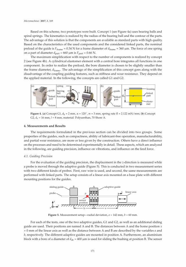
Micromachines 2017, 8, 169
Based on this scheme, two prototypes were built. Concept 1 (see Figure 4a) uses bearing balls andspiral springs. The kinematics is realized by the radius of the bearing ball and the contour of the parts.The advantage of this solution is that the components are available as standard parts with high quality.Based on the characteristics of the used components and the considered linked parts, the nominalpreload of the guide is Fframe = 0.34 N for a frame diameter of dframe = 360 µm. The force of one springon a part of diameter dpart = 660 µm is Fpart = 0.66 N.
The maximum simplification with respect to the number of components is realized by concept2 (see Figure 4b). A cylindrical elastomer element with a central bore integrates all functions in onecomponent. In order to realize the preload, the bore diameter is chosen to be slightly smaller thanthe frame diameter, dframe. The advantage of the simplification of this concept goes along with thedisadvantage of the coupling guiding features, such as stiffness and wear resistance. They depend onthe applied material. In the following, the concepts are called G1 and G2.
Figure 4. (a) Concept G1, db = 2 mm, α = 120◦, m = 3 mm, spring rate R = 2.122 mN/mm; (b) ConceptG2, de = 16 mm, l = 8 mm, material: Polyurethan, 70 Shore A.
4. Measurements and Results
The requirements formulated in the previous section can be divided into two groups. Someproperties of the guides, such as compactness, ability of lubricant-free operation, manufacturability,and partial wear resistance, are more or less given by the construction. Others have a direct influenceon the processes and need to be determined experimentally in detail. These aspects, which are analyzedin the following, are guiding precision, influence on vibrations, and influence on the feed force.
4.1. Guiding Precision
For the evaluation of the guiding precision, the displacement in the z-direction is measured whilea probe is moved through the adaptive guide (Figure 5). This is conducted in two measurement serieswith two different kinds of probes. First, raw wire is used, and second, the same measurements areperformed with linked parts. The setup consists of a linear axis mounted on a base plate with differentmounting positions for the guides.
Figure 5. Measurement setup—radial deviation, a = 142 mm, b = 60 mm.
For each of the tests, one of the two adaptive guides, G1 and G2, as well as an additional slidingguide are used. Their positions are named A and B. The distances between A and the home position x
= 0 mm of the linear axis as well as the distance between A and B are described by the variables a andb, respectively. The different adaptive guides are mounted in position A. Furthermore, an aluminiumblock with a bore of a diameter of dsb = 400 µm is used for sliding the bushing at position B. The sensor
171
Micromachines 2017, 8, 169
is located at position P, directly outside the adaptive guide. The position of the probe in the z-directionis measured by an optical micrometer (Figure 6). The accuracy of the used device is specified to0.7 µm. Between the single measurements, the probe is moved in the x-direction by the linear axis.The displacement between two measurements determines the measurement point distance ∆x relativeto the wire. The sensor detects the upper edge of the probe. Consequently, the measurements consideronly the z-direction. Assuming that the used probe is not rotationally symmetric, a different behaviorin the y- and z-directions is expected and the angular orientation of the probe around its length axis(x-axis) could influence the measurement results. Consequently, two measurements are performed foreach test configuration. First, a measurement with the same probe section and probe orientation isperformed for both guides. Following this, the probe is rotated 90◦ around its length axis (x-axis) andthe measurements are repeated. For each measurement, the probe is fed in fixed steps of distance ∆x
until reaching position x = 10 mm and measured for each step, before being pushed back to the startingposition. This measurement procedure is repeated 10 times. The radial deviation e is calculated byrelating each measurement to the initial value at the position of x = 0 mm. The centering force of theguides is assumed to be direction-independent. Hence, the orientation of the guides is considerednegligible. Nevertheless, G1 is oriented during testing in a way so that the uppermost of the threesprings is aligned with the z-axis.
Figure 6. Measurement setup—radial deviation.
For a proper interpretation of the measurements, it is important to distinguish different influences.One influence is expected to be the contour accuracy of the probe, which is not necessarily rotationallysymmetric. Therefore, the base material of the linked parts, which is hard-drawn wire (1.4301/AISI 304)with a diameter of dwire = 360 µm with bright surface produced in bars, is used instead of the linkedparts for the first experiments. The measurement point distance is set to ∆x = 1 mm. Figures 7 and 8illustrate the results. The range of the mean value from the minimum to the maximum is beneath10 µm for the orientation of 0◦ and beneath 5 µm for the orientation of 90◦ for both guides. Thestandard deviation of the measurements is close to the sensor resolution, but obviously smaller forguide G2. Within the diagrams, the measurements show a similar curve shape for the same angularorientation but different guides. Comparing the curve shapes between the two diagrams respectively,a clear difference can be observed between the different angular orientations. This can be explained bythe fact that even the raw wires show some contour deviations due to being not ideally straight androtationally symmetric.
Figure 7. Comparison of radial deviation for G1 and G2 measured with wire, dwire = 360 µm.
172
Micromachines 2017, 8, 169
Figure 8. Comparison of radial deviation for G1 and G2 measured with wire, dwire = 360 µm.
Finally, G1 and G2 are tested with real linked parts. For further identification of the influence ofthe contour of the parts, two different linked parts are used (Figure 9). Linked part 1 shows a goodrotational symmetry and no measurable offset op1 ≈ 0 µm between the two wires at both sides of thepart. Linked part 2, in contrast, shows an offset op2. The frame diameter of dframe = 360 µm and thepart diameter of dpart = 660 µm is equal in both cases. The length of the parts is lpart 1 ≈ 1200 µm andlpart 2 ≈ 1000 µm. The measurement procedure is the same as before, but the measuring point distanceis reduced to ∆x = 0.2 mm. Furthermore, the measurement is again performed two times for eachlinked part and, for the second measurement, the linked part is rotated 90◦ around its length axis(x-axis). The parts are illustrated in Figure 9 in both orientations. The measured offset of linked part 2is op2,0◦ = 165 µm for the orientation of 0◦ and op2,90◦ = 225 µm for the orientation of 90◦.
(a) (b)
(c) (d)
Figure 9. (a) Linked part 1 at 0◦, (b) Linked part 1 at 90◦, (c) Linked part 2 at 0◦, and (d) Linked part 2at 90◦.
In the measurements with G1 (Figure 10a), the regions where the bearing balls are in contact withthe parts can clearly be recognized by the unsteady curve. The range of the deviation is about 40 µmin the zones where only the wire is in contact with the bearing balls. The overall range of the deviationis about 160 µm. A similar behavior can be observed in the measurements for G2 (Figure 10b), but thecurve is smoother. The overall range of the deviation is about 50 µm. Before the part enters the guide(x = 1 mm) and after it has passed through (x = 9 mm), the deviation e is close to 0 µm. The curves forthe two different angular orientations are quite similar. As expected, the deviation for linked part 2is much higher and in a range of 225 µm (Figure 11). The deviation is on a constant level, when thepart is not within the guide, but there is a significant offset between the two described regions whenthe part is before and when it is behind the guide. For both guides, the curves are similar, but for G2,the curve is smoother and shows a smaller standard deviation.
173
Micromachines 2017, 8, 169
(a) (b)
Figure 10. Radial deviation for (a) G1 and (b) G2 measured with linked part 1 (no offset betweenwire ends).
(a) (b)
Figure 11. Radial deviation for (a) G1 and (b) G2 measured with linked part 2 (offset betweenwire ends).
4.2. Vibrations
For the vibration analysis, an application-specific testing is performed, which allows a qualitativecomparison of the different guide concepts under the aspect of suppression of radial vibrations(Figure 12).
174
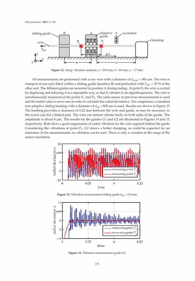
Micromachines 2017, 8, 169
Figure 12. Setup vibration analysis, a = 230 mm, b = 60 mm, p = 17 mm.
All measurements are performed with a raw wire with a diameter of dwire = 360 µm. The wire isclamped at one end, fitted within a sliding guide (position B) and preloaded with Fplv = 25 N at theother end. The different guides are mounted in position A during testing. At point S, the wire is excitedby displacing and releasing it in a repeatable way, so that it vibrates in its eigenfrequencies. The wire issimultaneously measured at the points P1 and P2. The same sensor in previous measurements is usedand the initial value is set to zero in order to calculate the radial deviation e. For comparison, a standardnon-adaptive sliding bushing with a diameter of dsg = 800 µm is used. Results are shown in Figure 13.The bushing provides a clearance of 0.22 mm between the wire and guide, as may be necessary inthe worst case for a linked part. The wire can almost vibrate freely on both sides of the guide. Theamplitude is about 8 µm. The results for the guides G1 and G2 are illustrated in Figures 14 and 15,respectively. Both show a good suppression of radial vibration for the wire segment behind the guide.Considering the vibrations at point P1, G2 shows a better damping, as could be expected for anelastomer. In the measurements, no vibration can be seen. There is only a variation in the range of thesensor resolution.
Figure 13. Vibration measurement sliding guide dsg = 0.8 mm.
Figure 14. Vibration measurement guide G1.
175
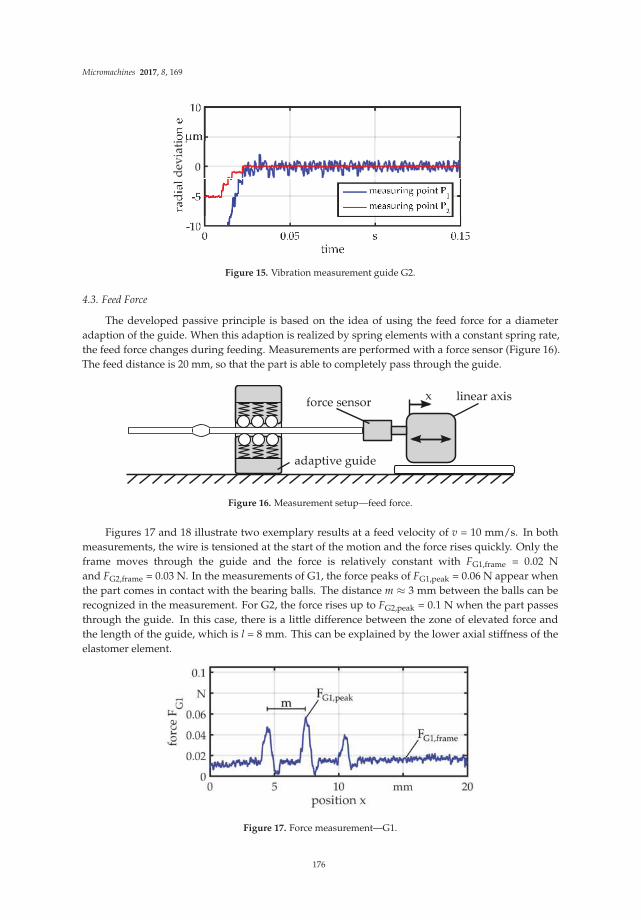
Micromachines 2017, 8, 169
Figure 15. Vibration measurement guide G2.
4.3. Feed Force
The developed passive principle is based on the idea of using the feed force for a diameteradaption of the guide. When this adaption is realized by spring elements with a constant spring rate,the feed force changes during feeding. Measurements are performed with a force sensor (Figure 16).The feed distance is 20 mm, so that the part is able to completely pass through the guide.
Figure 16. Measurement setup—feed force.
Figures 17 and 18 illustrate two exemplary results at a feed velocity of v = 10 mm/s. In bothmeasurements, the wire is tensioned at the start of the motion and the force rises quickly. Only theframe moves through the guide and the force is relatively constant with FG1,frame = 0.02 Nand FG2,frame = 0.03 N. In the measurements of G1, the force peaks of FG1,peak = 0.06 N appear whenthe part comes in contact with the bearing balls. The distance m ≈ 3 mm between the balls can berecognized in the measurement. For G2, the force rises up to FG2,peak = 0.1 N when the part passesthrough the guide. In this case, there is a little difference between the zone of elevated force andthe length of the guide, which is l = 8 mm. This can be explained by the lower axial stiffness of theelastomer element.
Figure 17. Force measurement—G1.
176
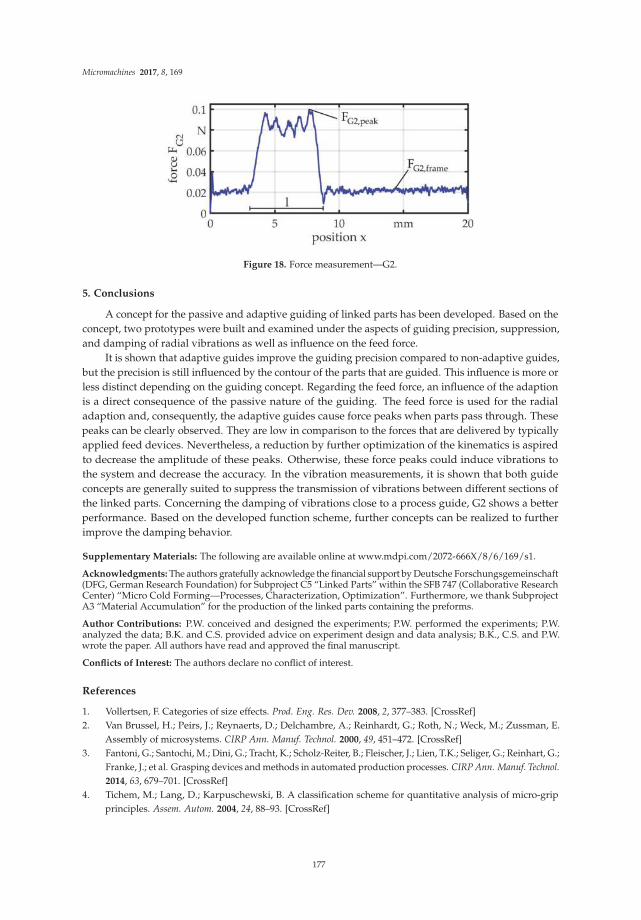
Micromachines 2017, 8, 169
Figure 18. Force measurement—G2.
5. Conclusions
A concept for the passive and adaptive guiding of linked parts has been developed. Based on theconcept, two prototypes were built and examined under the aspects of guiding precision, suppression,and damping of radial vibrations as well as influence on the feed force.
It is shown that adaptive guides improve the guiding precision compared to non-adaptive guides,but the precision is still influenced by the contour of the parts that are guided. This influence is more orless distinct depending on the guiding concept. Regarding the feed force, an influence of the adaptionis a direct consequence of the passive nature of the guiding. The feed force is used for the radialadaption and, consequently, the adaptive guides cause force peaks when parts pass through. Thesepeaks can be clearly observed. They are low in comparison to the forces that are delivered by typicallyapplied feed devices. Nevertheless, a reduction by further optimization of the kinematics is aspiredto decrease the amplitude of these peaks. Otherwise, these force peaks could induce vibrations tothe system and decrease the accuracy. In the vibration measurements, it is shown that both guideconcepts are generally suited to suppress the transmission of vibrations between different sections ofthe linked parts. Concerning the damping of vibrations close to a process guide, G2 shows a betterperformance. Based on the developed function scheme, further concepts can be realized to furtherimprove the damping behavior.
Supplementary Materials: The following are available online at www.mdpi.com/2072-666X/8/6/169/s1.
Acknowledgments: The authors gratefully acknowledge the financial support by Deutsche Forschungsgemeinschaft(DFG, German Research Foundation) for Subproject C5 “Linked Parts” within the SFB 747 (Collaborative ResearchCenter) “Micro Cold Forming—Processes, Characterization, Optimization”. Furthermore, we thank SubprojectA3 “Material Accumulation” for the production of the linked parts containing the preforms.
Author Contributions: P.W. conceived and designed the experiments; P.W. performed the experiments; P.W.analyzed the data; B.K. and C.S. provided advice on experiment design and data analysis; B.K., C.S. and P.W.wrote the paper. All authors have read and approved the final manuscript.
Conflicts of Interest: The authors declare no conflict of interest.
References
1. Vollertsen, F. Categories of size effects. Prod. Eng. Res. Dev. 2008, 2, 377–383. [CrossRef]
2. Van Brussel, H.; Peirs, J.; Reynaerts, D.; Delchambre, A.; Reinhardt, G.; Roth, N.; Weck, M.; Zussman, E.
Assembly of microsystems. CIRP Ann. Manuf. Technol. 2000, 49, 451–472. [CrossRef]
3. Fantoni, G.; Santochi, M.; Dini, G.; Tracht, K.; Scholz-Reiter, B.; Fleischer, J.; Lien, T.K.; Seliger, G.; Reinhart, G.;
Franke, J.; et al. Grasping devices and methods in automated production processes. CIRP Ann. Manuf. Technol.
2014, 63, 679–701. [CrossRef]
4. Tichem, M.; Lang, D.; Karpuschewski, B. A classification scheme for quantitative analysis of micro-grip
principles. Assem. Autom. 2004, 24, 88–93. [CrossRef]
177
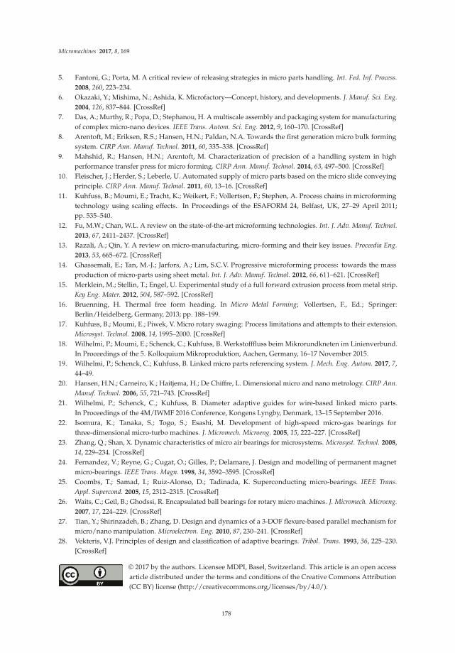
Micromachines 2017, 8, 169
5. Fantoni, G.; Porta, M. A critical review of releasing strategies in micro parts handling. Int. Fed. Inf. Process.
2008, 260, 223–234.
6. Okazaki, Y.; Mishima, N.; Ashida, K. Microfactory—Concept, history, and developments. J. Manuf. Sci. Eng.
2004, 126, 837–844. [CrossRef]
7. Das, A.; Murthy, R.; Popa, D.; Stephanou, H. A multiscale assembly and packaging system for manufacturing
of complex micro-nano devices. IEEE Trans. Autom. Sci. Eng. 2012, 9, 160–170. [CrossRef]
8. Arentoft, M.; Eriksen, R.S.; Hansen, H.N.; Paldan, N.A. Towards the first generation micro bulk forming
system. CIRP Ann. Manuf. Technol. 2011, 60, 335–338. [CrossRef]
9. Mahshid, R.; Hansen, H.N.; Arentoft, M. Characterization of precision of a handling system in high
performance transfer press for micro forming. CIRP Ann. Manuf. Technol. 2014, 63, 497–500. [CrossRef]
10. Fleischer, J.; Herder, S.; Leberle, U. Automated supply of micro parts based on the micro slide conveying
principle. CIRP Ann. Manuf. Technol. 2011, 60, 13–16. [CrossRef]
11. Kuhfuss, B.; Moumi, E.; Tracht, K.; Weikert, F.; Vollertsen, F.; Stephen, A. Process chains in microforming
technology using scaling effects. In Proceedings of the ESAFORM 24, Belfast, UK, 27–29 April 2011;
pp. 535–540.
12. Fu, M.W.; Chan, W.L. A review on the state-of-the-art microforming technologies. Int. J. Adv. Manuf. Technol.
2013, 67, 2411–2437. [CrossRef]
13. Razali, A.; Qin, Y. A review on micro-manufacturing, micro-forming and their key issues. Proceedia Eng.
2013, 53, 665–672. [CrossRef]
14. Ghassemali, E.; Tan, M.-J.; Jarfors, A.; Lim, S.C.V. Progressive microforming process: towards the mass
production of micro-parts using sheet metal. Int. J. Adv. Manuf. Technol. 2012, 66, 611–621. [CrossRef]
15. Merklein, M.; Stellin, T.; Engel, U. Experimental study of a full forward extrusion process from metal strip.
Key Eng. Mater. 2012, 504, 587–592. [CrossRef]
16. Bruenning, H. Thermal free form heading. In Micro Metal Forming; Vollertsen, F., Ed.; Springer:
Berlin/Heidelberg, Germany, 2013; pp. 188–199.
17. Kuhfuss, B.; Moumi, E.; Piwek, V. Micro rotary swaging: Process limitations and attempts to their extension.
Microsyst. Technol. 2008, 14, 1995–2000. [CrossRef]
18. Wilhelmi, P.; Moumi, E.; Schenck, C.; Kuhfuss, B. Werkstofffluss beim Mikrorundkneten im Linienverbund.
In Proceedings of the 5. Kolloquium Mikroproduktion, Aachen, Germany, 16–17 November 2015.
19. Wilhelmi, P.; Schenck, C.; Kuhfuss, B. Linked micro parts referencing system. J. Mech. Eng. Autom. 2017, 7,
44–49.
20. Hansen, H.N.; Carneiro, K.; Haitjema, H.; De Chiffre, L. Dimensional micro and nano metrology. CIRP Ann.
Manuf. Technol. 2006, 55, 721–743. [CrossRef]
21. Wilhelmi, P.; Schenck, C.; Kuhfuss, B. Diameter adaptive guides for wire-based linked micro parts.
In Proceedings of the 4M/IWMF 2016 Conference, Kongens Lyngby, Denmark, 13–15 September 2016.
22. Isomura, K.; Tanaka, S.; Togo, S.; Esashi, M. Development of high-speed micro-gas bearings for
three-dimensional micro-turbo machines. J. Micromech. Microeng. 2005, 15, 222–227. [CrossRef]
23. Zhang, Q.; Shan, X. Dynamic characteristics of micro air bearings for microsystems. Microsyst. Technol. 2008,
14, 229–234. [CrossRef]
24. Fernandez, V.; Reyne, G.; Cugat, O.; Gilles, P.; Delamare, J. Design and modelling of permanent magnet
micro-bearings. IEEE Trans. Magn. 1998, 34, 3592–3595. [CrossRef]
25. Coombs, T.; Samad, I.; Ruiz-Alonso, D.; Tadinada, K. Superconducting micro-bearings. IEEE Trans.
Appl. Supercond. 2005, 15, 2312–2315. [CrossRef]
26. Waits, C.; Geil, B.; Ghodssi, R. Encapsulated ball bearings for rotary micro machines. J. Micromech. Microeng.
2007, 17, 224–229. [CrossRef]
27. Tian, Y.; Shirinzadeh, B.; Zhang, D. Design and dynamics of a 3-DOF flexure-based parallel mechanism for
micro/nano manipulation. Microelectron. Eng. 2010, 87, 230–241. [CrossRef]
28. Vekteris, V.J. Principles of design and classification of adaptive bearings. Tribol. Trans. 1993, 36, 225–230.
[CrossRef]
© 2017 by the authors. Licensee MDPI, Basel, Switzerland. This article is an open access
article distributed under the terms and conditions of the Creative Commons Attribution
(CC BY) license (http://creativecommons.org/licenses/by/4.0/).
178

MDPI AG
St. Alban-Anlage 66
4052 Basel, Switzerland
Tel. +41 61 683 77 34
Fax +41 61 302 89 18
http://www.mdpi.com
Micromachines Editorial Office
E-mail: [email protected]
http://www.mdpi.com/journal/micromachines


MDPI AG
St. Alban-Anlage 66
4052 Basel
Switzerland
Tel: +41 61 683 77 34
Fax: +41 61 302 89 18
www.mdpi.com ISBN 978-3-03842-605-9
Copyright © 2022 FDOKUMEN