Diamond and carbon-derived vacuum micro- and nano-electronic devices
7
Diamond and carbon-derived vacuum micro- and nano-electronic devices W.P. Kang a, T , J.L. Davidson a , A. Wisitsora-at a , Y.M. Wong a , R. Takalkar a , K. Subramania a , D.V. Kerns b , W.H. Hofmeister c a Department of Electrical Engineering and Computer Science, Vanderbilt University, Nashville, TN 37235, USA b Olin College of Engineering, Needham, MA 02492, USA c Department of Chemical Engineering, Vanderbilt University, Nashville, TN 37235, USA Available online 17 March 2005 Abstract A bmorphologically engineeredQ fabrication approach has been utilized for the development various configurations of diamond/carbon field emitter arrays and devices. Based on this approach, we have developed several fabrication processes to micro-pattern diamond and other forms of carbon structures and achieve topologically managed field emitters that optimize both the geometrical and quantum aspects of the Fowler–Nordheim governed field emission. We report the fabrication of (a) pyramidal and edge-shaped vertical field emission devices, (b) lateral diamond field emission devices, (c) nano-patterned nano-scaled diamond field emitter arrays, and (d) gated carbon nanotubes field emitters. Excellent field emission device structures over a large area have been achieved with these fabrication methods. The interesting field emission results of these devices suggest the potential of diamond/carbon emission devices beyond conventional vacuum microelectronics is significant. D 2005 Elsevier B.V. All rights reserved. Keywords: Diamond/carbon; Carbon nanotubes; Field emission diode/triode; Vertical and lateral micro-arrays; Micro- and nano-patterning 1. Introduction Chemical vapor-deposited (CVD) diamonds or related carbons are excellent cathode materials for vacuum elec- tronics because of their low electron affinity and excellent mechanical and chemical properties. However, the bdirectQ usage of diamond or other forms of carbon emitters leads to non-uniform emitter microstructures, uncontrolled randomly scattered emission sites, and inconsistent emission behav- iors. Consequently, practical engineering design and control of emitter structures are needed to fully exploit the use of diamond/carbon field emitters. We have developed a molding process for the fabrication of diamond field emitter cathodes [1] and reported practical modifications involving the sp 2 content, boron doping, and tip sharpening to further enhance diamond field emission [2–5]. This paper describes the use of micro- and nano- fabrication methods to achieve various forms of diamond/ carbon bmorphologically engineeredQ structures such as vertically self-aligned gated micro pyramidal tips and micro edges, lateral micro emitter structures with built-in gate and anode, nano-scaled field emitter arrays, and gated carbon nanotubes (CNTs) arrays, for electron emission modulation and control. Vertically self-aligned gated diamond vacuum triodes were fabricated on a silicon-on-insulator (SOI) mold utilizing conventional silicon micro-patterning and etching techniques to define the anode, gate, and cathode. The fabrication has achieved diamond field emitter triodes over practical wafer areas. Lateral diamond vacuum devices were fabricated with a diamond patterning technique utilizing an oxide mask and lift-off. Nano-scaled diamond field emitter arrays were fabricated by focus ion beam (FIB) and nanocrystalline diamond deposition process. Gated carbon nanotubes field emission devices were achieved by catalytic-aided thermal CVD of CNTs on pre-defined cathode area on silicon substrate. Detail physical structures and field emission characteristics of these devices are presented. 0925-9635/$ - see front matter D 2005 Elsevier B.V. All rights reserved. doi:10.1016/j.diamond.2005.01.033 T Corresponding author. E-mail address: [email protected] (W.P. Kang). Diamond & Related Materials 14 (2005) 685 – 691 www.elsevier.com/locate/diamond
Transcript of Diamond and carbon-derived vacuum micro- and nano-electronic devices

www.elsevier.com/locate/diamond
Diamond & Related Materi
Diamond and carbon-derived vacuum micro- and nano-electronic devices
W.P. Kanga,T, J.L. Davidsona, A. Wisitsora-ata, Y.M. Wonga, R. Takalkara, K. Subramaniaa,
D.V. Kernsb, W.H. Hofmeisterc
aDepartment of Electrical Engineering and Computer Science, Vanderbilt University, Nashville, TN 37235, USAbOlin College of Engineering, Needham, MA 02492, USA
cDepartment of Chemical Engineering, Vanderbilt University, Nashville, TN 37235, USA
Available online 17 March 2005
Abstract
A bmorphologically engineeredQ fabrication approach has been utilized for the development various configurations of diamond/carbon
field emitter arrays and devices. Based on this approach, we have developed several fabrication processes to micro-pattern diamond and other
forms of carbon structures and achieve topologically managed field emitters that optimize both the geometrical and quantum aspects of the
Fowler–Nordheim governed field emission. We report the fabrication of (a) pyramidal and edge-shaped vertical field emission devices, (b)
lateral diamond field emission devices, (c) nano-patterned nano-scaled diamond field emitter arrays, and (d) gated carbon nanotubes field
emitters. Excellent field emission device structures over a large area have been achieved with these fabrication methods. The interesting field
emission results of these devices suggest the potential of diamond/carbon emission devices beyond conventional vacuum microelectronics is
significant.
D 2005 Elsevier B.V. All rights reserved.
Keywords: Diamond/carbon; Carbon nanotubes; Field emission diode/triode; Vertical and lateral micro-arrays; Micro- and nano-patterning
1. Introduction
Chemical vapor-deposited (CVD) diamonds or related
carbons are excellent cathode materials for vacuum elec-
tronics because of their low electron affinity and excellent
mechanical and chemical properties. However, the bdirectQusage of diamond or other forms of carbon emitters leads to
non-uniform emitter microstructures, uncontrolled randomly
scattered emission sites, and inconsistent emission behav-
iors. Consequently, practical engineering design and control
of emitter structures are needed to fully exploit the use of
diamond/carbon field emitters.
We have developed a molding process for the fabrication
of diamond field emitter cathodes [1] and reported practical
modifications involving the sp2 content, boron doping, and
tip sharpening to further enhance diamond field emission
[2–5]. This paper describes the use of micro- and nano-
fabrication methods to achieve various forms of diamond/
0925-9635/$ - see front matter D 2005 Elsevier B.V. All rights reserved.
doi:10.1016/j.diamond.2005.01.033
T Corresponding author.
E-mail address: [email protected] (W.P. Kang).
carbon bmorphologically engineeredQ structures such as
vertically self-aligned gated micro pyramidal tips and micro
edges, lateral micro emitter structures with built-in gate and
anode, nano-scaled field emitter arrays, and gated carbon
nanotubes (CNTs) arrays, for electron emission modulation
and control.
Vertically self-aligned gated diamond vacuum triodes
were fabricated on a silicon-on-insulator (SOI) mold
utilizing conventional silicon micro-patterning and etching
techniques to define the anode, gate, and cathode. The
fabrication has achieved diamond field emitter triodes over
practical wafer areas. Lateral diamond vacuum devices
were fabricated with a diamond patterning technique
utilizing an oxide mask and lift-off. Nano-scaled diamond
field emitter arrays were fabricated by focus ion beam
(FIB) and nanocrystalline diamond deposition process.
Gated carbon nanotubes field emission devices were
achieved by catalytic-aided thermal CVD of CNTs on
pre-defined cathode area on silicon substrate. Detail
physical structures and field emission characteristics of
these devices are presented.
als 14 (2005) 685–691

SiSiO2
SiO2
SiO2Si
(a)
(b) SiO2Si
SiSiO2
SiO2
(c) SiO2Si
SiSiO2
SiO2
(d)SiO2Si
SiSiO2
SiO2
Diamond
SiO2
SiSiO2
Diamond
SiO2
Si
Diamond
(e)
(f)
Fig. 1. The fabrication scheme of the vertical self-align gated diamond
emitter triode utilizing silicon-on-insulator wafer.
Si-Gate
Diamond Tip
(a)
(c)
Fig. 2. Scanning electron micrographs of: (a) diamond pyramidal tips array; (b) d
emitter structure with pyramidal tips; (d) vertical self-aligned gated diamond emi
W.P. Kang et al. / Diamond & Related Materials 14 (2005) 685–691686
2. Device fabrications, structures, and electron emission
characteristics
2.1. Vertical diamond field emission devices
The vacuum diode and triode in a vertical configuration
are robust electronic devices with high-speed capability,
high temperature, and radiation tolerance. These diamond
emitters have superior transistor performance. However,
there are challenging obstacles to the development of a
diamond field emitter triode due to the difficulty of diamond
processing to achieve the three-terminal structure.
We have developed a practical and well-controlled
micro-fabrication method that utilizes silicon-on-insulator
(SOI) wafer as a substrate with a self-contained basic triode
structures. Vertically self-aligned gated pyramidal-tip and
edge-shaped triode structures were fabricated on a silicon-
on-insulator (SOI) mold. This fabrication method (Fig. 1)
utilizes conventional silicon micro-patterning and etching
techniques to define the anode, gate, and cathode. Details of
the fabrication steps have been described in prior publica-
tions [1,5]. The fabrication has achieved pyramidal-shaped
(Fig. 2(a)) and edge-shaped (Fig. 2(b)) diamond field
emitter cathode arrays and self-aligned gated triodes (Fig.
(d)
(b)
iamond edge-shaped emitters array; (c) vertical self-aligned gated diamond
tter structure with edge-shaped emitters.

4.5
4
3.5
3
2.5
2
1.5
1
0.5
0
Ano
de C
urre
nt (
µA)
0 50 100 150 200 250 300 350
Anode Voltage (V)
Fig. 3. The anode emission current vs. anode voltage (Ia–Va) of a self-
aligned gated diamond emitter triode (with 4 tips).
(a)
W.P. Kang et al. / Diamond & Related Materials 14 (2005) 685–691 687
2(c)–(d)) over practical wafer areas. The SEM of the
fabricated diamond field emission triode structures show
the nano-sharp apex and edges, surrounded by a self-aligned
silicon gate derived from the process.
SiO2
SiO2
SiO2Si
Si
SiO2
SiO2Si
Si
SiO2
Anode pattern
Cathodepattern
SiO2
SiO2
Si
Si
SiO2
Diamond
SiO2
Si
Si
SiO2
Diamond
(a) Starting material: oxidized SOI wafer
(b) Oxide patterning for diamond cathode and anode
(c) PECVD diamond deposition
(d) SiO2 and Si etching to form diamond anode and cathode
Si
SiO2SiSiO2
DiamondAnode Cathode
Fig. 4. Fabrication process for lateral diamond emitter utilizing silicon-on-
insulator wafer.
The field emission of the self-aligned gated triode
exhibits transistor characteristics [5]. Ia–Vg–Va plots (Fig.
3) of emission characteristics from 4 tips show a very low
gate turn-on voltage of 10 V and high emission current of 4
AA at gate voltage of 20 V. Ia–Va plots of emission
characteristics demonstrate the desired saturation behavior
of field emission transistor with a high voltage gain of 250.
The high amplification factor value indicates that the
diamond field emission transistor provides high voltage
gain when operated as an amplifier. The low turn-on gate
voltage and high gain factor are comparable to solid-state
metal-oxide-semiconductor field effect transistor, MOSFET,
devices, confirming the diamond field emission triode has
significant potential for IC-compatible vacuum microelec-
tronic applications.
2.2. Lateral diamond vacuum devices
Field emission device in lateral configurations has
interest to vacuum microelectronics due to simpler fabrica-
tion, design versatility of electrode geometry, and precise
spacing between electrodes by fine photolithography con-
Diamond Anode
Diamond Cathode
SiO2
Diamond gate
Diamond gate
(b)
Diamond Anode
SiO2
Diamond Cathode
Fig. 5. Scanning electron micrographs of lateral diamond emitter structures:
(a) diode configuration and (b) triode configuration.

Fig. 6. The emission current vs. anode voltage of a lateral diamond emitter
diode (with 4 fingers). Insert is the F–N plot of the emission data.
W.P. Kang et al. / Diamond & Related Materials 14 (2005) 685–691688
trol. A number of lateral field emitters utilizing materials
other than diamond have been reported [6–12], but their
emission characteristics are marginal.
(e) Si mold removal
(d) Boron-doped Microcrystalline diamond growth us
(a) Starting material: 1 cm2 silicon sample
(b) Mold formation on silicon by high-precision millin
(c) Nanodiamond growth using CH4/H2/N2 PECVD d
Fig. 7. Fabrication process of the nanodiamond vacuum field emission
We have developed a lateral diamond emitter fabrica-
tion technique on a SOI wafer utilizing oxide patterning
and lift-off process. The fabrication steps for the lateral
diamond emitter are shown in Fig. 4. The process begins
with the growth of 1 Am SiO2 on a SOI wafer followed by
patterning the anode and cathode structures on the SiO2
layer. The exposed SiO2 was then etched away, and the
diamond grown on the silicon area by PECVD with bias-
enhanced nucleation. The SiO2 masking layer was etched
away. The patterned diamond anode and cathode served as
a mask for etching silicon to yield isolation between the
electrodes as well as setting the anode–gate–cathode
spacing. The final structure consists of patterned diamond
anode, gate, and cathode, supported by a silicon layer
underneath, sitting on the SiO2 layer on the silicon
substrate.
Fig. 5 shows lateral device structures in a diode and a
triode configuration. However, from the SEM micrograph
observation, it would be seem that the apparently large
radius curvature of the diamond finger cathode would be
further reduced. Application of sub-micron photolithogra-
phy patterning is of interest. More elaborate lateral config-
urations are conceived and under evaluation.
Preliminary emission test (Fig. 6) has shown the lateral
diode exhibits a low turn-on voltage of ~5 V and a high
emission current of 6 AA, from 4 diamond fingers, at an
anode voltage of 25 V. The emission current of the lateral
ing CH4/H2/TMB PECVD deposition technique
Si
g using the FIB
eposition technique
Si
Si
Nanodiamond
Microcrystalline diamond
Si
Nanodiamond
Diamond thin film with high aspect ratio nano-tips
cathode by the focused ion beam nano-mold transfer technique.

(a) (b)
Fig. 8. SEM micrographs of an array of high aspect-ratio diamond nano-tips array (a) low magnification and (b) high magnification.
Fig. 9. The emission current vs. anode voltage of a nano-diamond nano-tips
array.
W.P. Kang et al. / Diamond & Related Materials 14 (2005) 685–691 689
emitter conforms to F–N behavior (insert of Fig. 6) and thus
confirms that the observed current is electron field emission.
The emission current is stable over time, with current
fluctuation less than 10% over ~3 days, under a fixed anode
voltage. The low turn-on voltage (turn-on field ~3 V/Am)
and high emission characteristics are among the best of
reported lateral field emitter structures. The lateral diamond
field emitter has potential applications in vacuum micro-
electronics, sensors and microelectromechanical systems
(MEMS).
2.3. Nano-patterned nano-scaled diamond field emitter
arrays
We have recently developed a FIB (focused ion beam)
nano-mold transfer technique for the development of nano-
diamond vacuum field emission cathode arrays. The nano-
crystalline diamond grown by CH4/H2/N2 MPCVD was
applied for the fabrication of a field emission nano-cathode
array. The fabrication process steps are outlined in Fig. 7.
An n-type silicon substrate of area 1 cm2 is the starting
material. The nano-mold is then created on the silicon
substrate by high precision milling using a focused ion
beam, whereby a finely focused beam of gallium (Ga+) ions
are rastered on the surface of the silicon, forming arrays of
high aspect-ratio conical cavities of controlled diameter and
depth. Nanocrystalline diamond film is then deposited in
and on the silicon mold by the CH4/H2/N2 CVD process.
The mold-filling is followed by a thicker layer of micro-
crystalline diamond film deposited using CH4/H2/Trime-
thylboron CVD process. Next, a metal layer such as Ti/Ni
(~1 Am) is deposited on the diamond film, which is then
brazed with high-temperature copper alloy [Cu(26.7%)/
Ti(4.5%)/Ag(68.8%)] ~500 Am thick on a Mo substrate in a
vacuum of ~10�6 Torr at 900 8C. The final process step is to
flip the chip and completely etch remove the silicon using
KOH solution, which yields a diamond thin film with high
aspect-ratio nano-tips.
Fig. 8 includes the SEM micrographs displaying an array
of high aspect-ratio diamond nano-tips fabricated by nano-
crystalline diamond growth in and on the inverted silicon
molds. The radius of curvature of the diamond nano-tip
shown in the figure is less than 30 nm. The aspect ratio of
the tips is about 25 and 37 in specific cases. The diamond
nano-tips, as seen in the figure, take the contour of the
cavities created in the silicon mold by the FIB. The diamond
nano-tip array cathode was examined for enhanced electron
field emission. Fig. 9 shows a low turn-on field of ~4 V/Amand a high current density of ~2 A/cm2 have been be
achieved. The novel FIB nano-mold transfer technique is a
step towards the development of vacuum bnanoelectronicQdevices.

W.P. Kang et al. / Diamond & Related Materials 14 (2005) 685–691690
2.4. Carbon nanotubes field emission devices
Carbon nanotubes field emission devices are attractive
due to the simplicity of carbon nanotubes synthesis and the
compatibility of using conventional silicon micro-patterning
technique for the fabrication of CNTs vacuum devices. We
have presented the development of thermal CVD grown
carbon nanotubes (CNTs) for cold cathode applications [13].
We have recently developed a fabrication process for gated
CNTs, configured as triode field emitter.
The gated field emitter or triode device was fabricated
utilizing conventional silicon IC fabrication process. The
SiO2
Si
Gate
SiO2
Si
Dry Oxidation
Sputtering of Metal Gate
SiO2
SiO2
SiO2
Si
Gate Gate
PR PR
Patterning & Wet-etching of Metal
SiO2
(a)
(b)
(c)
(d
(e
(f
(g)
Self-aligned Gate
CNTs
Fig. 10. (a)–(f) Schematic diagram of the fabrication process for the single-mask
over-etched gate.
fabrication process is a single-mask, self-aligned integrated
gate electrode triode structure, as illustrated in Fig. 10(a)–
(f). The process begins with thermal oxidation of highly
doped n-type silicon (100) substrate followed by sputter-
deposition of the gate metal (gold or copper). The thickness
of the thermal oxide and the sputtered metal layers was ~1.5
Am and 0.8 Am, respectively. After that, the metal gate and
the oxide were isotropically wet-etched. Next, a thin layer of
Ti and Pd was sputter-deposited in sequence. Following
that, the unwanted catalyst above the gate layer was lifted
off with acetone. Lastly, the mold was transferred to the
CVD chamber for selective growth of CNTs inside the
Gate
SiO2
PR
Gate
SiO2
PR
Si
Sputtering of catalysts
Wet-etching of SiO2 (BOE)
Gate
SiO2
PR
Gate
SiO2
PR
Si
Catalysts Lift-off & Growth of CNTs
Gate
SiO2
Gate
SiO2
Si
)
)
)
self-aligned 3-band triode structure, and (g) SEM of the 3-band triode with
0.0
0.5
1.0
1.5
2.0
2.5
3.0
25 50 75 100 125 150 175 200
Va (V)
I a(µ
A)
Vg = 50 V
Vg = 65 V
Vg = 80 V
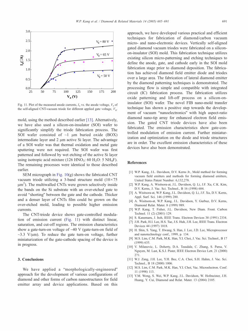
Fig. 11. Plot of the measured anode currents, Ia vs. the anode voltage, Va of
the self-aligned CNT-vacuum triode for different applied gate voltage, Vg.
W.P. Kang et al. / Diamond & Related Materials 14 (2005) 685–691 691
mold, using the method described earlier [13]. Alternatively,
we have also used a silicon-on-insulator (SOI) wafer to
significantly simplify the triode fabrication process. The
SOI wafer consisted of ~1 Am buried oxide (BOX)
intermediate layer and 2 Am active Si layer. The advantage
of a SOI wafer was that thermal oxidation and metal gate
sputtering were not required. The SOI wafer was first
patterned and followed by wet etching of the active Si layer
using isotropic acid mixture (126 HNO3: 60 H2O: 5 NH4F).
The remaining processes were identical to those described
earlier.
SEM micrograph in Fig. 10(g) shows the fabricated CNT
vacuum triode utilizing a 3-band structure mold (10�75
Am2). The multiwalled CNTs were grown selectively inside
the bands on the Si substrate with an over-etched gate to
avoid bshortingQ between the gate and the cathode. Thicker
and a denser layer of CNTs film could be grown on the
over-etched mold, leading to possible higher emission
currents.
The CNT-triode device shows gate-controlled modula-
tion of emission current (Fig. 11) with distinct linear,
saturation, and cut-off regions. The emission characteristics
show a gate-turn-on voltage of ~40 V (gate-turn-on field of
~3.3 V/Am). To reduce the gate turn-on voltage, further
miniaturization of the gate-cathode spacing of the device is
in progress.
3. Conclusions
We have applied a bmorphologically-engineeredQapproach for the development of various configurations of
diamond and other forms of carbon nanostructures for field
emitter array and device applications. Based on this
approach, we have developed various practical and efficient
techniques for fabrication of diamond/carbon vacuum
micro- and nano-electronic devices. Vertically self-aligned
gated diamond vacuum triodes were fabricated on a silicon-
on-insulator (SOI) mold. This fabrication technique utilizes
existing silicon micro-patterning and etching techniques to
define the anode, gate, and cathode early in the SOI mold
fabrication stage prior to diamond deposition. The fabrica-
tion has achieved diamond field emitter diode and triodes
over a large area. The fabrication of lateral diamond emitter
by the diamond patterning techniques is demonstrated. The
processing flow is simple and compatible with integrated
circuit (IC) fabrication process. The fabrication utilizes
oxide patterning and lift-off process on a silicon-on-
insulator (SOI) wafer. The novel FIB nano-mold transfer
technique has shown a positive step towards the develop-
ment of vacuum bnanoelectronicsQ with high aspect-ratio
diamond nano-tip array for enhanced electron field emis-
sion. The gated CNT triode devices have also been
fabricated. The emission characteristics show gate-con-
trolled modulation of emission current. Further miniatur-
ization and optimization on the diode and triode structures
are in order. The excellent emission characteristics of these
devices have also been demonstrated.
References
[1] W.P. Kang, J.L. Davidson, D.V. Kerns Jr., Mold method for forming
vacuum field emitters and methods for forming diamond emitters,
United States Patent Number: 6,132,278.
[2] W.P. Kang, A. Wisitsora-at, J.L. Davidson, Q. Li, J.F. Xu, C.K. Kim,
D.V. Kerns, J. Vac. Sci. Technol., B 16 (1998) 684.
[3] A. Wisitsora-at, W.P. Kang, J.L. Davidson, Q. Li, J.F. Xu, D.V. Kerns,
Appl. Surf. Sci. 146 (1999) 280.
[4] A. Wisitsora-at, W.P. Kang, J.L. Davidson, Y. Gurbuz, D.V. Kerns,
Diamond Relat. Mater. 8 (1999) 989.
[5] W.P. Kang, T. Fisher, J.L. Davidson, New Diam. Front. Carbon
Technol. 11 (2) (2001) 129.
[6] S. Kanemaru, J. Itoh, IEEE Trans. Electron Devices 38 (1991) 2334.
[7] J.H. Park, H.I. Lee, H.S. Tae, J.S. Huh, J.H. Lee, IEEE Trans. Electron
Devices 44 (1997) 1018.
[8] H. Shin, S. Yang, T. Hwang, S. Han, J. Lee, J.D. Lee, Microprocessor
and nanotechnology conf., 1999, p. 134.
[9] M.S. Lim, C.M. Park, M.K. Han, Y.I. Choi, J. Vac. Sci. Technol., B 17
(1999) 635.
[10] V. Milanovic, L. Doherty, D.A. Teasdale, C. Zhang, S. Parsa, V.
Nguyen, M. Last, K.S.J. Pister, IEEE Electron Device Lett. 21 (2000)
271.
[11] W.J. Zang, J.H. Lee, Y.H. Bee, C.A. Choi, S.H. Hahm, J. Vac. Sci.
Technol., B 18 (2000) 1006.
[12] M.S. Lim, C.M. Park, M.K. Han, Y.I. Choi, Vac. Microelectron. Conf.
11 (1998) 113.
[13] Y.M. Wong, S. Wei, W.P. Kang, J.L. Davidson, W. Hofmeister, J.H.
Huang, Y. Cui, Diamond and Relat. Mater. 13 (2004) 2105.