In-Beam Diamond Start Detectors
11
IEEE TRANSACTIONS ON NUCLEAR SCIENCE 1 In-Beam Diamond Start Detectors M. Ciobanu * , E. Berdermann, N. Herrmann, K.D. Hildenbrand, M. Kiš, W. Koenig, J. Pietraszko, M. Pomorski, M. Rebisz-Pomorska, A. Schüttauf Abstract—This paper describes operation principles and the in- beam performance of Start Detector (SD) assemblies consisting of Diamond Detectors (DDs) grown by Chemical Vapour Deposition (CVD) and Front End Electronics (FEE) which have been designed for and used in various nuclear physics experiments at GSI Helmholtz Center for Heavy Ion Research in Darmstadt. In parallel to the FEE design we have performed extensive calculations to model the dependence of the signal-to-noise ratio (S/N ) and the time resolution σt on various quantities such as the collected charge Qcol , the detector capacitance CD, the temperature T , and finally the noise contribution and bandwidth of the amplifier. In combination with the new FEEs (including an application- specific integrated circuit, ASIC) we have tested both poly- crystalline and single-crystal diamonds of various sizes and thicknesses with relativistic ion beams ranging from protons to heaviest ions. For heavy ions all setups deliver time resolutions σt < 60 ps. In case of protons the small primary detector signals require single-crystals as material and more elaborated designs like segmentation of the detector area and the increase of the amplifier input impedance. The best time resolution obtained for relativistic protons was σt = 117 ps. Index Terms—Detector instrumentation, Analog integrated circuits, Timing circuits, Timing electronics I. I NTRODUCTION A n in in-beam Start Detector (SD) is an important com- ponent of Time-of-Flight (TOF) systems, which are commonly used to identify different reaction products in fixed- target nuclear physics experiments. It provides the time-zero Manuscript received September 24, 2010; revised February 10, 2011 and April 17, 2011; accepted June 05, 2011. This work was supported in part by the European Community through the FP6 Integrated Infrastructure Initiative Hadron Physics, Proj. RII3-CT-2004-506078 and in part by the German BMBF under the project number 06HD154. M. Ciobanu is with the GSI Helmholtz Zentrum für Schwerionenforschung GmbH, 64291 Darmstadt, Germany. He is also with the Space Sciences Institute, 077125 Bucharest, Romania (email: [email protected]). E. Berdermann, K. D. Hildenbrand, W. Koenig and A. Schüttauf are with the GSI Helmholtz Zentrum für Schwerionenforschung GmbH, 64291 Darmstadt, Germany (e-mail: [email protected]; [email protected]; [email protected]; [email protected]). N. Herrmann is with the Physikalisches Institut der Universität Heidelberg, 69120 Heidelberg, Germany (e-mail: [email protected]). M. Kiš is with the GSI Helmholtz Zentrum für Schwerionenforschung GmbH, 64291 Darmstadt, Germany. He is also with the Ru ¯ der Boškovi´ c Institute, 10000 Zagreb, Croatia (email: [email protected]). J. Pietraszko is with the Institut für Kernphysik der Johann Wolfgang Goethe Universität Frankfurt, 60438 Frankfurt am Main, Germany (email: [email protected]). M. Pomorski and M. Rebisz-Pomorska are now with the Diamond Sensor Laboratory of CEA-LIST Saclay, F-91191 Gif-sur-Yvette, France (e-mails: [email protected], [email protected]). Color versions of one or more of the figures in this paper are available online at http://ieeexplore.ieee.org. Digital Object Identifier 10.1109/TNS.2011.2160282 (T 0) or reference time for the TOF measurement by deter- mining the crossing time of each beam particle before it hits the target. So the uncertainty in T 0 affects directly the TOF resolution and hence the velocity and the mass identification [1]. In order to reach TOF resolutions below 100 ps, the time resolution σ t of the SD must be below the half of that value. In addition, another feature may be of importance: high beam intensities require fast detectors delivering narrow signals and electronics which can cope with the corresponding rates. In connection with this the material should be radiation hard to withstand high integral doses without sizeable degradation of its properties. In the next section we describe briefly the physical param- eters of diamonds, which make them an almost ideal active detector material to meet the mentioned requirements. A prerequisite, however, is an optimal adaptation of the used FEE. In order to understand better the underlying relations and dependencies of parameters, such as the signal-to-noise ratio S/N and the time resolution σ t on various system parameters, we have performed model calculations the results of which have influenced especially the design of the detectors for minimum-ionizing protons. Formalism and the results are described in section III.We start with the simplest model of readout electronics (just one resistor) to evaluate the dependence of S/N and σ t on the collected charge Q col , on the detector capacitance C D and on the temperature T . In a few steps we add the contribution of the amplifier noise and its bandwidth, resulting in a set of analytical formulae describing the dependence of S/N and σ t on these parameters. Two extreme cases are discussed: The hypothetically instantaneous charge collection and the more realistic case of charge drift to the opposite electrodes. In section IV we present several SD-setups, which have been designed for different experiments, and their resolutions σ t which have been achieved with various beams of relativistic ions. All diamonds used in the present studies have been grown at Element Six Ltd. (King’s Ride Park, Ascot, Berkshire SL58BP, UK) and supplied by DIAMOND DETECTORS LTD (16 Fleetsbridge Business Centre, Upton Road, Ponte, Dorset BH17AF, UK). We investigated both types: polycrystalline diamond detectors (pcDD) grown on silicon wafers and single- crystal diamond detectors (scDD) grown on mono-crystalline {100}-oriented High-Pressure-High-Temperature (HPHT) syn- thetic diamond substrates. II. CVD DIAMONDS AS DETECTOR MATERIAL 0018–9499$26.00 c 2011 IEEE
-
Upload
independent -
Category
Documents
-
view
1 -
download
0
Transcript of In-Beam Diamond Start Detectors

IEEE TRANSACTIONS ON NUCLEAR SCIENCE 1
In-Beam Diamond Start DetectorsM. Ciobanu∗, E. Berdermann, N. Herrmann, K.D. Hildenbrand, M. Kiš, W. Koenig, J. Pietraszko, M. Pomorski,
M. Rebisz-Pomorska, A. Schüttauf
Abstract—This paper describes operation principles and the in-beam performance of Start Detector (SD) assemblies consisting ofDiamond Detectors (DDs) grown by Chemical Vapour Deposition(CVD) and Front End Electronics (FEE) which have beendesigned for and used in various nuclear physics experimentsat GSI Helmholtz Center for Heavy Ion Research in Darmstadt.
In parallel to the FEE design we have performed extensivecalculations to model the dependence of the signal-to-noise ratio(S/N ) and the time resolution σt on various quantities suchas the collected charge Qcol, the detector capacitance CD , thetemperature T , and finally the noise contribution and bandwidthof the amplifier.
In combination with the new FEEs (including an application-specific integrated circuit, ASIC) we have tested both poly-crystalline and single-crystal diamonds of various sizes andthicknesses with relativistic ion beams ranging from protons toheaviest ions.
For heavy ions all setups deliver time resolutions σt < 60 ps.In case of protons the small primary detector signals requiresingle-crystals as material and more elaborated designs likesegmentation of the detector area and the increase of the amplifierinput impedance. The best time resolution obtained for relativisticprotons was σt = 117 ps.
Index Terms—Detector instrumentation, Analog integratedcircuits, Timing circuits, Timing electronics
I. INTRODUCTION
An in in-beam Start Detector (SD) is an important com-ponent of Time-of-Flight (TOF) systems, which are
commonly used to identify different reaction products in fixed-target nuclear physics experiments. It provides the time-zero
Manuscript received September 24, 2010; revised February 10, 2011 andApril 17, 2011; accepted June 05, 2011. This work was supported in part bythe European Community through the FP6 Integrated Infrastructure InitiativeHadron Physics, Proj. RII3-CT-2004-506078 and in part by the GermanBMBF under the project number 06HD154.
M. Ciobanu is with the GSI Helmholtz Zentrum für SchwerionenforschungGmbH, 64291 Darmstadt, Germany. He is also with the Space SciencesInstitute, 077125 Bucharest, Romania (email: [email protected]).
E. Berdermann, K. D. Hildenbrand, W. Koenig and A. Schüttauf arewith the GSI Helmholtz Zentrum für Schwerionenforschung GmbH, 64291Darmstadt, Germany (e-mail: [email protected]; [email protected];[email protected]; [email protected]).
N. Herrmann is with the Physikalisches Institut der Universität Heidelberg,69120 Heidelberg, Germany (e-mail: [email protected]).
M. Kiš is with the GSI Helmholtz Zentrum für SchwerionenforschungGmbH, 64291 Darmstadt, Germany. He is also with the Ruder BoškovicInstitute, 10000 Zagreb, Croatia (email: [email protected]).
J. Pietraszko is with the Institut für Kernphysik der Johann WolfgangGoethe Universität Frankfurt, 60438 Frankfurt am Main, Germany (email:[email protected]).
M. Pomorski and M. Rebisz-Pomorska are now with the Diamond SensorLaboratory of CEA-LIST Saclay, F-91191 Gif-sur-Yvette, France (e-mails:[email protected], [email protected]).
Color versions of one or more of the figures in this paper are availableonline at http://ieeexplore.ieee.org.
Digital Object Identifier 10.1109/TNS.2011.2160282
(T0) or reference time for the TOF measurement by deter-mining the crossing time of each beam particle before it hitsthe target. So the uncertainty in T0 affects directly the TOFresolution and hence the velocity and the mass identification[1]. In order to reach TOF resolutions below 100 ps, the timeresolution σt of the SD must be below the half of that value.In addition, another feature may be of importance: high beamintensities require fast detectors delivering narrow signals andelectronics which can cope with the corresponding rates. Inconnection with this the material should be radiation hard towithstand high integral doses without sizeable degradation ofits properties.
In the next section we describe briefly the physical param-eters of diamonds, which make them an almost ideal activedetector material to meet the mentioned requirements.
A prerequisite, however, is an optimal adaptation of the usedFEE. In order to understand better the underlying relations anddependencies of parameters, such as the signal-to-noise ratioS/N and the time resolution σt on various system parameters,we have performed model calculations the results of whichhave influenced especially the design of the detectors forminimum-ionizing protons.
Formalism and the results are described in section III.Westart with the simplest model of readout electronics (just oneresistor) to evaluate the dependence of S/N and σt on thecollected charge Qcol, on the detector capacitance CD and onthe temperature T . In a few steps we add the contribution ofthe amplifier noise and its bandwidth, resulting in a set ofanalytical formulae describing the dependence of S/N and σton these parameters. Two extreme cases are discussed: Thehypothetically instantaneous charge collection and the morerealistic case of charge drift to the opposite electrodes. Insection IV we present several SD-setups, which have beendesigned for different experiments, and their resolutions σtwhich have been achieved with various beams of relativisticions.
All diamonds used in the present studies have been grownat Element Six Ltd. (King’s Ride Park, Ascot, BerkshireSL58BP, UK) and supplied by DIAMOND DETECTORS LTD(16 Fleetsbridge Business Centre, Upton Road, Ponte, DorsetBH17AF, UK). We investigated both types: polycrystallinediamond detectors (pcDD) grown on silicon wafers and single-crystal diamond detectors (scDD) grown on mono-crystalline100-oriented High-Pressure-High-Temperature (HPHT) syn-thetic diamond substrates.
II. CVD DIAMONDS AS DETECTOR MATERIAL
0018–9499$26.00 c© 2011 IEEE

2 IEEE TRANSACTIONS ON NUCLEAR SCIENCE
I n comparison to any other known detector material, di-amond features a high mobility for both carriers, which
can be derived from the field-dependent carrier drift velocitiesν(E)e,h measured with broadband amplifiers (BBA) apply-ing the Transient Current Technique (TCT) with short-rangeα-particles [2]. Note that the FWHM of the TCT signalsrepresents the carriers transition time ttr = d/ν(E)e,h withthe detector thickness d, whereas the signal area correspondsto Qcol. The directly measured mobility values obtained byone of the authors for scDD at lowest possible electric fieldsED are µe = 1800 cm2/Vs and µh = 2450 cm2/Vs atED = 0.1 V/µm and ED = 0.06 V/µm, respectively [3]. Thesemobilities in conjunction with very high breakdown fieldsEbreak > 107 V/cm and a low dielectric constant εr = 5.7provide detector signals of fast rise times and narrow pulsewidths suitable for fast timing and counting of high ion rates.Moreover, diamond is radiation hard [4], most likely due to thehigh atomic packing factor of the carbon atoms in the diamondlattice causing strong covalent bonds. The same origin compelsa wide band gap (Eg = 5.48 eVT=300K), which providesdiamond sensors of very low dark current but also of high pairproduction energy εDia ≈ 13 eV, and thus of relatively lowsensitivity, e.g. compared to silicon (εSi ≈ 3.6 eV). Its thermalconductivity (20 Wcm−1K−1), which is six times higher thanthat of copper, supports self-annealing of shallow traps andprotects in-beam detectors against thermal spikes.
In scDDs, practically 100% of the generated primary chargeis collected. In pcDD a part of this charge is lost at grainboundaries resulting in reduced charge collection efficienciesCCE = Qcol/Qgen between 0.1 and 0.6 (with Qgen the iongenerated charge). Due to the current production technologyhowever, the size of standard scDDs do not exceed 5 mm x5 mm, which is given by the dimensions of the HPHT diamondsubstrates used for the epitaxial growth. The maximum areaavailable so far may reach 10 mm x 10 mm.
For precise calculations of the amplitudes of signals emittedby relativistic heavy ions in diamond sensors of different qual-ity, the transient current signal shape has to be known; suchsimulations are not available at present. Hence, we estimatedroughly the pulse heights delivered by two diamond detectors(DD) of 300 µm thickness on the 50 Ω input impedance of aBBA, taken into account signal widths (FWHM) of 2.5 ns and1.5 ns for a scDD (CCE = 1) and a pcDD (CCE = 0.4),respectively [5].
The results plotted in Fig. 1 have been calculated forparticles of 1 A GeV kinetic energy. The horizontal solidline indicates the equivalent noise amplitude of the diamondbroadband amplifier (DBA) [6], i.e. σnDBA ≈ 50 µV, whereasthe dashed line the 3σnDBA deviation noise amplitude. Fig. 1illustrates the large dynamic range of signals expected inhadron physics experiments. Furthermore, it shows that theBBA readout in the case of relativistic ions lighter thancarbon is challenging even for spectroscopic grade single-crystal diamond sensors.
III. HOW CAN THE DETECTION OF RELATIVISTIC PROTONSBE IMPROVED?
Fig. 1. Estimated pulse heights on the input of a BBA. The data have beencalculated for various relativistic heavy ions of a kinetic energy of 1 A GeVtraversing two DDs of d = 300 µm and CCE = 0.4 and 1.0, respectively.
Cc
(b)
Vout Vout
TR
Ri CiIbb
Rb
Cb
TRi (t)
CD
Ri CiCD
i (t)
VV
Rb
Ibb
(a)
Fig. 2. Schematic layout of two circuits for the connection of a DD to itsamplifier (see text for explanation).
F ig. 2 shows the two FEE schematics, which are mostfrequently used to read out DDs: (a) one DD electrode is
connected to ground; the second one is biased and read out,(b) one electrode is biased, the second one read out. The biasis applied by the power supply Vb via resistor Rb. In mode (b),the capacitor Cb decouples the biasing resistor thus eliminatingits thermal noise. Due to the high volume resistivity of thematerial, the breakdown voltage is very high and the leakagecurrent at nominal operation bias is negligible. The equivalentschematic comprises a pure capacitor and a current generator.
A. Signal Processing at Instantaneous Collection of Charge
In the following we will calculate the S/N using the sim-plified schematics shown in Fig. 3. The diamond detector isconnected to the simplest measurement system representedby the resistor Ri. This approach is similar to: "S/N versusCapacitance in a Current-Sensing Amplifier" [7], [8] and wewill continue with the evaluation of the time resolution σt.
This schematics represents a low pass filter with a timeconstant τS = RiCD and a cut-off frequency fS = 1/(2πτS).
inRiTRi
D VinpRiC
(t)
Fig. 3. Simplified equivalent schematic for noise estimations: the detector(dashed box) is connected to a simple measurement device represented by theresistor Ri.
CIOBANU et al.: IN-BEAM DIAMOND START DETECTORS 3
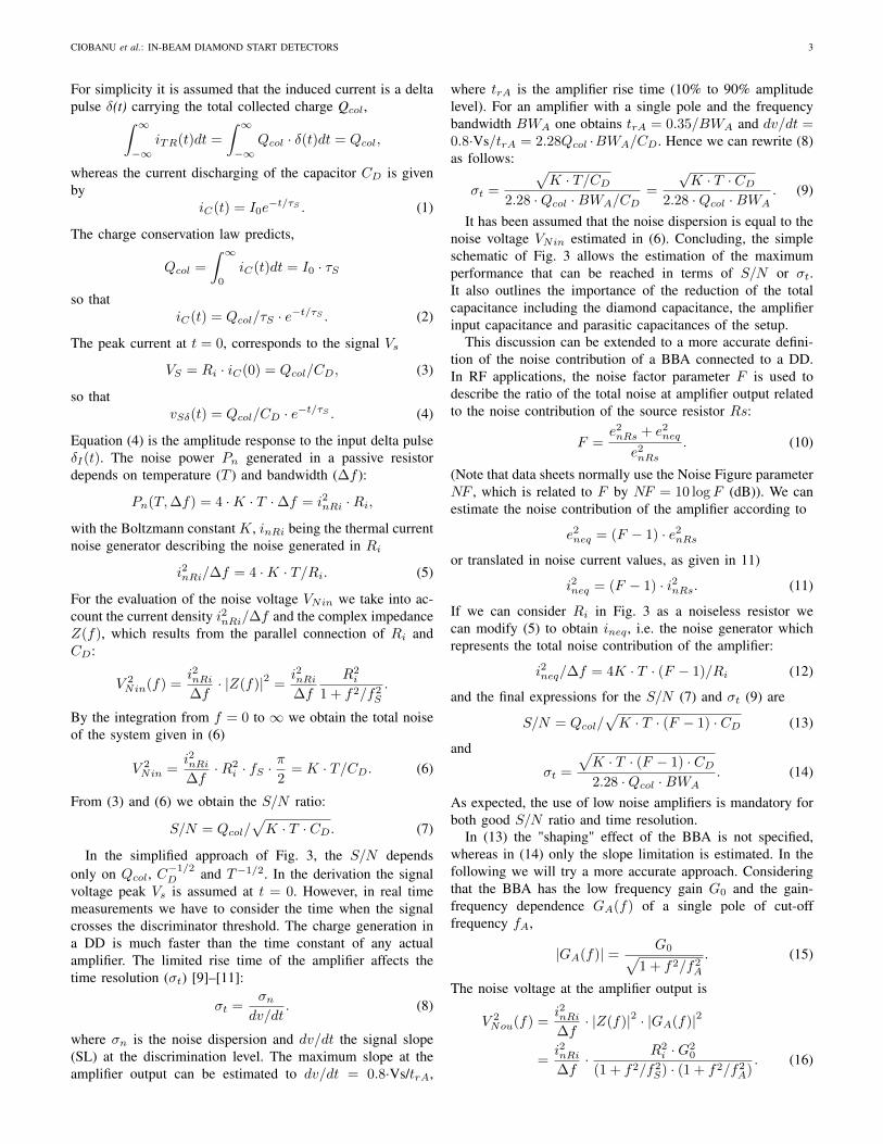
For simplicity it is assumed that the induced current is a deltapulse δ(t) carrying the total collected charge Qcol,∫ ∞
−∞iTR(t)dt =
∫ ∞−∞
Qcol · δ(t)dt = Qcol,
whereas the current discharging of the capacitor CD is givenby
iC(t) = I0e−t/τS . (1)
The charge conservation law predicts,
Qcol =
∫ ∞0
iC(t)dt = I0 · τS
so thatiC(t) = Qcol/τS · e−t/τS . (2)
The peak current at t = 0, corresponds to the signal Vs
VS = Ri · iC(0) = Qcol/CD, (3)
so thatvSδ(t) = Qcol/CD · e−t/τS . (4)
Equation (4) is the amplitude response to the input delta pulseδI(t). The noise power Pn generated in a passive resistordepends on temperature (T ) and bandwidth (∆f ):
Pn(T,∆f) = 4 ·K · T ·∆f = i2nRi ·Ri,
with the Boltzmann constant K, inRi being the thermal currentnoise generator describing the noise generated in Ri
i2nRi/∆f = 4 ·K · T/Ri. (5)
For the evaluation of the noise voltage VNin we take into ac-count the current density i2nRi/∆f and the complex impedanceZ(f), which results from the parallel connection of Ri andCD:
V 2Nin(f) =
i2nRi∆f· |Z(f)|2 =
i2nRi∆f
R2i
1 + f2/f2S.
By the integration from f = 0 to ∞ we obtain the total noiseof the system given in (6)
V 2Nin =
i2nRi∆f·R2
i · fS ·π
2= K · T/CD. (6)
From (3) and (6) we obtain the S/N ratio:
S/N = Qcol/√K · T · CD. (7)
In the simplified approach of Fig. 3, the S/N dependsonly on Qcol, C
−1/2D and T−1/2. In the derivation the signal
voltage peak Vs is assumed at t = 0. However, in real timemeasurements we have to consider the time when the signalcrosses the discriminator threshold. The charge generation ina DD is much faster than the time constant of any actualamplifier. The limited rise time of the amplifier affects thetime resolution (σt) [9]–[11]:
σt =σn
dv/dt. (8)
where σn is the noise dispersion and dv/dt the signal slope(SL) at the discrimination level. The maximum slope at theamplifier output can be estimated to dv/dt = 0.8·Vs/trA,
where trA is the amplifier rise time (10% to 90% amplitudelevel). For an amplifier with a single pole and the frequencybandwidth BWA one obtains trA = 0.35/BWA and dv/dt =0.8·Vs/trA = 2.28Qcol ·BWA/CD. Hence we can rewrite (8)as follows:
σt =
√K · T/CD
2.28 ·Qcol ·BWA/CD=
√K · T · CD
2.28 ·Qcol ·BWA. (9)
It has been assumed that the noise dispersion is equal to thenoise voltage VNin estimated in (6). Concluding, the simpleschematic of Fig. 3 allows the estimation of the maximumperformance that can be reached in terms of S/N or σt.It also outlines the importance of the reduction of the totalcapacitance including the diamond capacitance, the amplifierinput capacitance and parasitic capacitances of the setup.
This discussion can be extended to a more accurate defini-tion of the noise contribution of a BBA connected to a DD.In RF applications, the noise factor parameter F is used todescribe the ratio of the total noise at amplifier output relatedto the noise contribution of the source resistor Rs:
F =e2nRs + e2neq
e2nRs. (10)
(Note that data sheets normally use the Noise Figure parameterNF , which is related to F by NF = 10 logF (dB)). We canestimate the noise contribution of the amplifier according to
e2neq = (F − 1) · e2nRsor translated in noise current values, as given in 11)
i2neq = (F − 1) · i2nRs. (11)
If we can consider Ri in Fig. 3 as a noiseless resistor wecan modify (5) to obtain ineq , i.e. the noise generator whichrepresents the total noise contribution of the amplifier:
i2neq/∆f = 4K · T · (F − 1)/Ri (12)
and the final expressions for the S/N (7) and σt (9) are
S/N = Qcol/√K · T · (F − 1) · CD (13)
and
σt =
√K · T · (F − 1) · CD2.28 ·Qcol ·BWA
. (14)
As expected, the use of low noise amplifiers is mandatory forboth good S/N ratio and time resolution.
In (13) the "shaping" effect of the BBA is not specified,whereas in (14) only the slope limitation is estimated. In thefollowing we will try a more accurate approach. Consideringthat the BBA has the low frequency gain G0 and the gain-frequency dependence GA(f) of a single pole of cut-offfrequency fA,
|GA(f)| = G0√1 + f2/f2A
. (15)
The noise voltage at the amplifier output is
V 2Nou(f) =
i2nRi∆f· |Z(f)|2 · |GA(f)|2
=i2nRi∆f· R2
i ·G20
(1 + f2/f2S) · (1 + f2/f2A). (16)

4 IEEE TRANSACTIONS ON NUCLEAR SCIENCE
By integration of (16) from f = 0 to ∞ we obtain the totalnoise at the amplifier output (17)
V 2Nou =
i2nRi∆f·R2
i ·G20 · fS ·
fAfS + fA
· π2
=K · T · (F − 1) ·G2
0
CD · (1 + τA/τS)=K · T · (F − 1) ·G2
0
CD · (1 +m), (17)
where m = τA/τS . The response vAδ(t) of the amplifier tothe delta function excitation δ(t) is
vAδ(t) = VA · e−t/τA , (18)
with ∫ ∞0
vAδ(t)dt = VA · τA = G0. (19)
For the evaluation of the output signal, we have to use theconvolution of the signal vSδ(t) developed on Ri (3) withvAδ(t) given in (18):
vout(t) = vSδ(t)⊗ vAδ(t) =
∫ ∞−∞
vSδ(u)vAδ(t− u)du
= VS · VA · e−t/τA ·∫ t
0
eu(1/τA−1/τS)du.
a) for the particular case of τA = τS
vout(t) = VS · VA · e−t/τA · t =QcolCD· G0
τA· e−t/τA · t. (20)
vout(t) has a maximum for tM = τA
vout(tM ) =QcolCD· G0
e.
b) for τA 6= τS
vout(t) =QcolCD·G0 ·
τSτS − τA
· (e−t/τS − e−t/τA). (21)
vout(t) is maximal for
tM =ln τA
τS
1/τS − 1/τA= τA
lnm
m− 1. (22)
If we can measure the peak value vout(tM ) by peak detectionwe find
vout(tM ) =QcolCD·G0 ·
1
1−m·(e
m·lnm1−m − e
lnm1−m
)(23)
VNou = G0 ·
√K · T · (F − 1)
CD · (1 +m). (24)
We can calculate the S/N ratio;a) for the particular case τA = τS
S/N =Qcol√
K · T · (F − 1) · CD·√
1 +m
e. (25)
b) for τA 6= τS
S/N =Qcol√
K · T · (F − 1) · CD·
·√
1 +m
1−m·(e
m·lnm1−m − e
lnm1−m
). (26)
Fig. 4. S/N (left) and σt (right) as a function of CD with Ri as parameter.
In order to obtain σt we must calculate the slope SL ofvout(t) in the discrimination point, e.g. for simplicity at tD =tM/2 :
SL(t) =d(vout(t))
dt
=QcolCD·G0 ·
τSτS − τA
·(e−t/τA
τA− e−t/τS
τS
).
For tD = tM/2:
SL(tD) =QcolCD· G0
τA· 1
1−m·
·(e
lnm2·(1−m) −m · e
m·lnm2·(1−m)
),
σt =τA ·
√K · T · (F − 1) · CD
Qcol· 1−m√
1 +m·
· 1
elnm
2·(1−m) −m · em·lnm2·(1−m)
. (27)
Equations (26) and (27) represent the ideal case of a Diracexcitation where the charge is instantaneously collected. InFig. 4, S/N (26) and σt (27) are plotted as a function ofCD for three values of Ri (50 Ω, 500 Ω, and 5 kΩ). In thisevaluation the following parameters have been used: Qcol =2 fC, τA = 50 ps, F = 3.2, G0 = 20.
The S/N increases continuously with decreasing detectorcapacitance. The influence of the Ri value is minimal forCD > 1 pF (τS > τA) and vanishes for CD ≈ 10 pF. Theballistic deficit of the preamplifier generates an important lossof the signal amplitude for CD < 1 pF (τS < τA), which canbe compensated by an increase of Ri, leading to an increase ofS/N . The time resolution σt degrades linearly with increasingdetector capacitance and increasing Ri value.
For the calculations of the dependence of S/N and σton τA (Fig. 5), the following parameters have been used:Qcol = 2 fC, Ri = 50 Ω, F = 3.2, G0 = 20. BothS/N and σt improve significantly for low capacitances andlow τA values. The bandwidth of the low noise amplifierneeded is technologically limited to a few GHz at present(e.g. BW = 3.018 GHz, corresponding to a time constantof τA = 50 ps). Therefore, the most effective way forimprovement is a decrease of the total capacitance.
Fig. 6, 7 and 8 show results of simulations with theAPLAC simulation engine [12]. Detectors of capacitancesCD = 0.1 pF, 1 pF and 10 pF, respectively, have beenassumed, all readout with BBA (Fig. 2 left). The transientsignals on the detector (VS , left scale) are represented by full

CIOBANU et al.: IN-BEAM DIAMOND START DETECTORS 5
symbols, those at the amplifier output (VA, right scale) byopen symbols; a very fast injected charge has been assumed(2 fC in 0.2 ps). The time axis is in logarithmic scale. In eachfigure three values of Ri are plotted: 50 Ω (squares), 500 Ω(circles) and 5 kΩ (triangles). In all cases, τA =50 ps. Themaximum signal amplitude is obtained for minimum detectorcapacitance CD =0.1 pF (Fig.6). Nevertheless, it is obviousthat all cases show ballistic deficits (note the different Y-scalesand remember the amplifier gain G0 =20).
The minimum ballistic deficit is observed for CD = 10 pF(Fig. 8), but the signals are very small in this case. The designvalues of CD and Ri have to be a compromise between themost effective charge collection, the ballistic deficit and thehigh rate capability of the sensors.
B. Signal Processing at Complete Charge Drift and Collection
According to the Shockley-Ramo theorem, charge move-ment induces a time dependent current on the detector elec-trodes. For parallel plate detector geometry and under the as-sumption of a homogeneously distributed space charge withina scDD, the induced current can be described by the simplifiedformula (28) [2], [3]:
ie,h(t) =Qgen · v(E)e,h
det/τeff−t/τe,h , (28)
where Qgen is the generated charge, v(E)e,h is the chargecarrier velocity, d is the detector thickness, τe,h denotes thelifetime of excess electrons and holes and τeff is given by
τeff =ε · ε0
q · µe,h ·Neff. (29)
Neff denotes the net effective fixed space charge in thediamond bulk, ε the diamond permittivity, ε0 the vacuumpermittivity and q the elementary charge. If a negligibleamount of space charge is present, the internal electric fieldis almost constant. If the charge carrier lifetime τe,h is longerthen the transition time ttr, the carrier drift velocity vdr canbe calculated by vdr = d/ttr. In this case, a constant inducedcurrent is expected for 0 < t < ttr:
ie,h(t) =Qgenttr
= const.
Equations (20) and (21) represent the response of the wholesystem to the pulse Qcol · δ(t); in order to obtain the responseto 1 · δ(t) we must normalize
voutδ(t) = vout(t)/Qcol. (30)
Fig. 5. S/N (left) and σt (right) as a function of τA with CD as parameter.
Fig. 6. Simulated signals of a DD with CD =0.1 pF. Full symbols denote thedetector output signals (left ordinate), open symbols the corresponding BBAoutput signals (right ordinate). Three different values of Ri are considered(50 Ω, 500 Ω, and 5 kΩ) corresponding to τS =5 ps, 50 ps and 500 ps,respectively.
Fig. 7. Same as Fig.6 but for CD =1 pF and τS =50 ps, 500 ps and 5 ns.
To obtain the amplifier response vP (t) to ie,h(t), we use theconvolution
vP (t) = voutδ(t)⊗ ie,h(t) =
∫ t
0
voutδ(u) · ie,h(t− u)du.
For a) t ≤ ttr
vP (t) =Qgen ·G0
CD· τSttr·(me−t/τA − e−t/τS + 1−m
)1−m
(31)
Fig. 8. Same as Fig. 6 but for CD = 10 pF and τS = 500 ps, 5 ns and50 ns.

6 IEEE TRANSACTIONS ON NUCLEAR SCIENCE
Fig. 9. Transient response of a scDD with ttr = 5 ns and three values ofCD (0.1 pF, 1 pF and 10 pF), for Ri = 50 Ω (upper-left), Ri = 500 Ω(upper-right) and Ri = 5 kΩ (bottom).
and b) t > ttr
vP (t) =Qgen ·G0
CD· τSttr·[−e−t/τS + e−(t−ttr)/τS
1−m+
+m ·
(e−t/τA − e−(t−ttr)/τA
)1−m
]. (32)
Fig.9 shows the signal response at the output of a BBA (32)for a diamond detector of CD = 0.1 pF (squares), 1 pF (dots)and 10 pF (triangles), respectively. The upper-left figure iscalculated for an Ri = 50 Ω, the upper-right for Ri = 500 Ωand the bottom one for Ri = 5 kΩ.
We can estimate the signal amplitude as well as S/N andσt for t = ttr
vP (ttr) =Qgen ·G0
CD· τSttr·[m · e−ttr/τA − e−ttr/τS
1−m+ 1
]S/N =
Qgen√K · T · (F − 1) · CD
·√
1 +m
1−m· τSttr·
·(−e−ttr/τS +m · e−ttr/τA + 1−m
)(33)
SL(t) =d(vP (t))
dt=Qgen ·G0
CD · ttr· e−t/τS − e−t/τA
1−m.
This formula has a maximum for t = tM (22) when tD =tM/2,
SL(tD) =QgenCD
· G0
ttr· 1
1−m· (e
m·lnm2·(1−m) − e
lnm2·(1−m) )
σt =ttr ·
√K · T · (F − 1) · CD
Qgen· 1−m√
1 +m·
· 1
em·lnm2·(1−m) − e
lnm2·(1−m)
. (34)
We use (33) and (34) to evaluate the most difficult case, i.e.close to the detection of relativistic protons. The followingparameters have been used in Fig. 10: single crystal with
Fig. 10. S/N ratio (left) and σt (right) as a function of CD for three Ri
values.
Fig. 11. S/N ratio (left) and σt (right) as a function of τA, for three valuesof CD .
ttr = 5 ns, Qcol = 2 fC, τA = 50 ps, F = 3.2, G0 = 20,ttr = 5 ns. The S/N is less than 1 for any CD if Ri = 50 Ω(left). The increase of Ri to 500 Ω allows a S/N > 3 forCD > 2 pF and shows a maximum for CD ≈ 9 pF, whenτS = RiCD = 4.5 ns ≈ ttr. In the case of Ri = 5 kΩ,an optimum situation can be reached for CD ≈ 0.9 pF whenτS = 4.5 ns ≈ ttr.
Concluding, the S/N has an optimum for τS ≈ ttr i.e. whenthe detector time constant equals the carrier drift time.σt has also a strong dependence on CD, hence the decrease
of the detector capacitance is mandatory. Fig. 11 demonstratesthat in the case of Ri = 50 Ω there is no way to obtain areasonable S/N and σt for fast protons by selecting valuesfor τA and CD.
IV. APPLICATIONS
O ver the past years we have designed and constructeda number of SDs for various experiments at GSI. The
present material is meant as a comprehensive description of thework we have performed. Some parts may have been presentedelsewhere, in particular details of our FEE designs: these casesare properly referenced.
In the following, we give a short overview of these designsand the test results obtained with relativistic beams rangingfrom protons to tantalum ions. The results of the modelsimulations presented above served as a guideline for thevarious projects, especially for the design of proton detectors.
A new diamond SD for the FOPI (FOur PI) detector [13],was planned to replace the standard plastic scintillation startdetector. At that time only pcDDs were available in thenecessary size; for readout, discrete amplifiers (FEE-1-cards[11]) were used. The results were more than encouraging;

CIOBANU et al.: IN-BEAM DIAMOND START DETECTORS 7
Particle
D2A2
A1
Vthr
Start
Start
TD1
TD2
StopDEL2
DEL1 StopD1
t2
t1
t2
t1
t3 t2
t3 t1
t1
t2
Pasive Delay
ORt3
SD 1 SD 2
Fig. 12. Circuit for the measurement of the time resolution of SDs. Twoidentical detector channels are used (see text).
excellent time resolutions have been obtained. Details aredescribed in section IV-A.
Hence, we began to design an even larger system, whichincluded also beam-halo detectors surrounding the central SD(subsection B). The influence of all relevant capacitances tothe resolution was demonstrated in the model results; so wetried to reduce the external capacitances by replacing thediscrete FEE through the newly developed ASIC PADI-1. Ithouses three channels designed in a spirit very close to thatof the discrete FEE-1 amplifiers [14]. This allowed placingthe diamond SD directly on a printed-circuit board, whichcarries also the amplifier and discrimination system in veryclose environment.
Considering the model results and the resolutions reachedwith heavy ions it was obvious that decent results for protonswould clearly need single-crystal instead of polycrystallinematerial. The available areas of about 22 mm2 would presentalready too large capacitance, so the surface had to be seg-mented and the amplifier had to be placed extremely close tothe electrodes. Different technical approaches are described insubsections C and D; this last design was developed to be usedin the HADES experiment [15] at GSI.
The time resolutions of the various DD/FEE assemblieshave always been measured in the following way: two identicalSDs were placed one behind another in the direct beam; ina special experiment the second sensor was replaced by afast scintillation counter. The generalized setup is shown inFig. 12. The signals of the two SDs were processed by FEE,which was housing an amplifier (A) followed by a leadingedge discriminator (D). The OR signals provide the commonstart signal of the Time-to-Digital Converters (TD1, TD2) andtwo passively delayed signals (DEL) stop the individual TDchannels. The time-difference spectrum (i.e. the histogram ofthe time difference tD = ∆t1 − ∆t2 = t1 − t2 can beapproximated with a normal distribution of standard deviationσTD. Assuming equal contributions of the two identical SDs,the time resolution of one channel is given by σt = σTD/
√2.
Since the total capacitance of the setup is of high impor-tance, we discuss CD in the following in more detail. Thecapacitance of a round disk capacitor of radius a, thickness d,and dielectric constant εr can be calculated according to [16]:
CD =a2πε0εr
d
1 +
2d
πεra
[ln( a
2d
)+ (1.41εr + 1.77) +
Fig. 13. The pcDD set used in a 181Ta beam of 1 A GeV (left). The timedifference spectrum measured between two identical detectors (right). Thetime resolution is 22 ps.
+d
a(0.268εr + 1.65)
]. (35)
The first term represents the bulk capacitance defined onlyby the two circular electrodes; the fringe fields are describedby the other terms and account for up to 20% of CD.For other shapes and geometries, the share of the fringecapacitance may be even higher; it can be estimated on thebasis of approximating formulae or by simulation programs.We decided to measure the total detector capacitance CD;we used Boonton Capacitance Meter Model 72BD. In thefollowing, we will specify CD by two values: the estimatedvalue CDE , which ignores the fringe effects and the measuredvalue CDM , which is the total value including all assemblycapacitances: the detector bulk capacitance plus fringe as wellas the parasitic and the preamplifier input capacitances (notbiased) for the FEE located close to the DD.
A. Start Detectors for Heavy Ions
As a new in-beam SD for the FOPI experiment, a pcDD hasbeen mounted in the center of an aluminum box (Fig.13, leftphoto); metallized mylar entrance and exit windows close thebox. The crystal has an area of 10 mm x 10 mm, a thicknessof 0.5 mm, and it is fixed on a ceramic substrate. Each surfaceis covered by a round Cr/Au-electrode of 8 mm diameter(CDE = 5.14 pF, CDM = 6.8 pF), one being used as HV-electrode, the other for readout (cf. the two BNC connectors atthe bottom of the box). For timing tests, two FEE-1 cards [11],each consisting of four discrete channels of high-frequencyamplifiers followed by fast leading edge discriminators, areused to readout two identical detector modules placed onebehind the other perpendicular to the beam direction.
Using 181Ta beam of 1 A GeV, a time resolution σt ≈ 22 pswas measured (Fig. 13, right plot); a similar value (σt ≈ 28 ps)has been obtained with 27Al ions of 2 A GeV.
B. An Integrated Universal Beam Monitor and Start Detectorfor Heavy-Ion Experiments
After the positive results obtained from our first SD test(subsection IV-A) we designed a new assembly, in order tomeet all the requirements of a start system of the FOPIexperiment. The size of the pcDD was as large as 20 mm

8 IEEE TRANSACTIONS ON NUCLEAR SCIENCE
Fig. 14. Board comprising the 20 mm x 20 mm pcDD and the completeelectronics including two ASIC chips. The DD is divided into nine separatesegments for timing measurement and beam monitoring (see text for details).
Fig. 15. Time difference spectrum measured with the central pad of theDD of Fig. 14 in coincidence with a plastic scintillation detector. The DDplus FEE contributes with σt = 45 ps to the total σTD = 60 ps of the ToFspectrum.
x 20 mm; it is only 0.15 mm thick in order to reducebeam straggling and reactions in the detector material. It hasidentical aluminum contacts on front and back side, consistingof a central electrode of 5.5 mm diameter (CDE = 7.7 pF,CDM = 9.2 pF) for the start signal, four surrounding sectorsfor beam-profile measurements or beam-halo control, plus an-other segmented outermost ring (cf. Fig. 14). The latter servesmerely as a potential ring to guarantee the field homogeneityalong the borders of the beam-halo electrodes.
In order to minimize the capacitances the FEE is equippedwith two PADI-1 chips [14]; all components are mountedtogether with the DD on a common printed circuit board in adense configuration.
Each PADI-1 chip has three preamplifier-discriminatorchannels followed by digital buffers, which are used forreadout and processing of the signals of the five detectorsegments; the digitization is performed with external units.
This setup has been used in an experiment with a 1.9 A GeV58Ni beam. The time resolution was measured in referenceto the standard FOPI start detector, i.e. a plastic scintillationdetector, read out by two fast phototubes [13]; the resolutionof each sensor can be determined independently. From themeasured total sTD = 60 ps (Fig. 15), σt = 45 ps areattributed to the diamond setup.
The rate capability of PADI-1 has been investigated in abeam test experiment with carbon ions using a scDD of 3 mmx 3 mm area. The diamond sensor of 0.3 mm thickness wasmetallized with four circular pad electrodes on both sides, eachof 1.2 mm diameter and of capacitances CDE = 0.18 pF
Q1
BF998
To next Cell
Rload
1n 100n
Rbias
Ubias
S
D
To Detector
100K
G1
G2
Coax Cable
Fig. 16. Schematics of the MOS buffer.
and CDM = 2.9 pF, respectively. We observed a lineardependence of the detected rate on the beam intensity up to1.35 × 108 ions/spill. For details see [17], [18].
C. Start Detectors for Relativistic Light Ions and ProtonsFeaturing a Simple MOS Buffer.
The model calculations as well as the experimental resultsdescribed so far showed clearly that good time resolutions forlight ions, and in particular protons, demand additional designimprovement: one has to consequently minimize all relevantcapacitances of the assemblies, to increase the preamplifierinput impedance, and, above all, to use single-crystal diamondas detector material.
For a first beam test, the electrodes of two scDDs (of area= 4 mm x 4 mm and thickness d = 0.4 mm) have beensegmented into four sectors, each of those directly bondedto the corresponding input of its amplifier, which was locatedin close proximity of the sensor. We have chosen the BFR998double-gate MOS transistor which is often used in VHF/UHFamplifiers since it has a very good noise figure (typically0.6 dB@200 MHz and 1 dB@800 MHz) and a BW = 1 GHz.In addition, it has an input capacitance Ci = 1.2-2.4 pF,an output capacitance Cout = 1 pF, a feedback capacitanceCG1D < 25 fF and a transconductance of gm ≈ 25 mA/V.The DC bias and the detector signal are transmitted througha 50 Ω coaxial cable to a modified version of the FEE-1 [11]which contains also the biasing circuit. The simple MOS buffer(MB) circuit (Fig. 16) allows to easily adjusting the detectortime constant (in this case τS ≈ (CDE+ 2 pF )× 100 kΩ).The resulting capacitances per sector were CDE = 0.2 pF andCDM = 3.3 pF.
Fig. 17 shows the time difference spectrum measured withtwo well-aligned opposite sectors of the two quadrant sensors,which were mounted in short distance between each otherperpendicular to a 6Li beam of 1.8 A GeV. The time resolutionobtained was σt = 55 ps.
However, this simple MOS buffer solution has two draw-backs: Ci (≈ 2 pF) is not sufficiently low, and, since the gainis below 1.0, the noise of the next cell must be low too.
D. The new scDD Proton Start Detector for HADES
In the design described in the following, the above disadvan-tages have been eliminated. For the new proton start detectorfor the HADES spectrometer at GSI, the segmentation of thesensor electrode has been driven even further: the scDD of4.7 mm x 4.7 mm area and d = 0.5 mm thickness is segmented

CIOBANU et al.: IN-BEAM DIAMOND START DETECTORS 9
Fig. 17. Time difference spectrum measured with relativistic 6Li ions of1.8 A GeV using the MOS buffer plus the FEE-1 card and scDD sc3 (Table II).
Fig. 18. The new SD of HADES is a scDD of 4.7 mm x 4.7 mm size anda thickness of 500 µm; it is segmented in eight pads.
in eight pads (Fig. 18) yielding CDE = 0.142 pF andCDM = 1.5 pF. The new FEE consists of a low capacitancebroadband amplifier (LCB) for the first stage mounted closeto the sensor [19].
Fig. 19 shows the used FEE schematic. The low capacitancebroadband amplifier (LCB) consists of a 14 GHz widebandsilicon planar transistor mounted in common-emitter con-figuration. It is mounted as close as possible to the cor-responding pad of the segmented electrode. This transistorhas a low noise figure (NF = 1 dB) as well as lowcollector-base (CCBS = 0.13 pF) and emitter-base capaci-tances (CEBS = 0.22 pF). The biasing resistor is divided inthree elements to minimize the total parasitic capacitance. Thecollector load resistor is located at the input of the next cell.
The left-hand side photograph of Fig. 20 shows the FEEboard with its eight LCB channels before the mounting andbonding of the DD shown in Fig. 19 into the central hole.The identical electronics scheme was used to test a secondSD assembly, which was consisting of a sensor with one
Rload
1n 100n
Rbias
Ubias
Q1
100K
100K
100K
To next CellCoax Cable
To Detector BFG410W
Fig. 19. Schematics of the low capacitance broadband amplifier FEE.
Fig. 20. Mounting details of the LCB: at left is shown the PCB with 8channels used in the proton beam test and on the right one, a quadrant-SD(sc4, Table II) surrounded by four LCB amplifiers, as used in a 6Li beamtest.
Fig. 21. Time resolution measured with 6Li ions of 1.8 A GeV betweentwo segments of two different scDD (sc4, Table II), read out with thelow capacitance broadband amplifiers (LCB) developed for the HADESspectrometer.
electrode segmented in four sectors (quadrant detector sc4,Table II). Its board is shown on the right side of Fig. 20 withthe SD mounted in the right hole. The collectors of the LCBamplifiers are connected through micro strip lines to coaxialcables, which transmit the signals to the next amplifier cells.The PCB material is Rogers 4003C, a high-frequency material(glass-reinforced hydrocarbon and ceramics) with a dielectricconstant εr = 3.38±0.05. In order to minimize the detectorfringe capacitance, the ground plane has a circular groove cutaround the detector.
Two identical single-crystal diamond quadrant sensors (cs4,Table II) were tested with 6Li ions of 1.8 A GeV and antime resolution σt = 32 ps (Fig. 21) was achieved. Thiscan be compared to the 55 ps measured in the same beamtest with the simplified MOS-buffer FEE type of subsectionIV-C (Fig. 17). The eight-sector SD delivered with protons of3.5 GeV a resolution σt = 117 ps, which is the best protonvalue, reached so far [19].
V. SUMMARY AND CONCLUSIONS.
In this paper we describe a variety of detector systems con-sisting of diamond detectors and their front-end electronics,
which we have designed and built as in-beam start detectorsfor existing and future GSI experiments. They should be ableto cope with all beams of relativistic ions including protons,the detection of which is a particular challenge because of thevery low primary charge generated in the detector material.

10 IEEE TRANSACTIONS ON NUCLEAR SCIENCE
TABLE ITIME RESOLUTIONS OF VARIOUS ASSEMBLIES TESTED WITH VARIOUS
BEAMS AND BEAM ENERGIES
Ion: Type, Energy FEE type σt EFF DD(ps) (%) No.
p, 1.25 GeV TCSA+FEE-1 330 96 sc1p, 3.5 GeV LCB+FEE HA 117 94 sc2
6Li, 1.8 A GeV MB+FEE-1 55 no sc36Li, 1.8 A GeV LCB+FEE HA 32 no sc427Al, 2 A GeV FEE-1 28 92 pc158Ni, 1.9 A GeV PADI-1 45 no pc2181Ta, 1 A GeV FEE-1 22 94 pc3
TABLE IIDETAILS OF THE TESTED DD
DD Size d No. of Pad Area CDE CDM
No. (mm2) (mm) Pads (mm2) (pF) (pF)sc1 4 x 4 0.5 4 1.69 0.165 1.2sc2 4.7 x 4.7 0.5 8 1.46 0.142 1.5sc3 4 x 4 0.4 4 1.69 0.2 3.3sc4 3.5 x 3.5 0.05 4 1.43 1.4 2.5pc1 10 x 10 0.5 1 52.8 5.14 6.8pc2 20 x 20 0.15 9 23.8 7.7 9.2pc3 10 x 10 0.5 1 52.8 5.14 6.8
In parallel, we have performed extensive model calculationsto estimate the dependence of the signal-to-noise ratio S/Nand the time resolution σt on various parameters. The compu-tation results presented in detail in section III, together with themeasured resolutions of scDDs and pcDDs, show that a minordecrease of the total system capacitance CD and an increaseof the amplifier input resistance Ri alone are not sufficient forproton detection. CD has to be minimized by a) an extremelycareful design of the DD-FEE assembly, where especially thefirst stage of the FEE has to be positioned as close as possibleto the DD, b) a minimization of fringing detector capacitances(for which the mounting PCB should have the ground layersat a few mm distance) and c) by segmentation of the DDinto single pads, not exceeding a few mm2. When CD isminimized, the input resistance Ri can be adjusted to obtainthe optimum condition for S/N : τS ≈ ttr. In addition, oneshould use only single-crystal detectors, which collect almost100% of the primary charge.
Table I summarizes the experimental results obtained withthe diamond detectors described in Table II: the time resolu-tions σt achieved with the presented DD-FEE assemblies invarious beam tests with relativistic ions of different energies,and the detection efficiencies (EFF, if measured).
The tested scDDs and pcDDs are labeled sci and pci withi as running number; the FEE types are given as they aredenominated in the text. Along with the DD-FEE assembliesdescribed in section IV, we present the results of an early testperformed with a scDD assembly (sc1, TableII) equipped witha FEE consisting of a fast charge sensitive amplifier (TCSA)[20] as a first stage followed by a FEE-1 card.
The pc diamond SDs read out with FEE-1 or PADI-1 ASICsdeliver satisfying resolutions for relativistic heavy-ions in theorder of σt ≈ 45 ps. The sc diamond SDs have demonstratedtime resolutions σt < 60 ps with 6Li, 12C and 27Al ions.
The best value obtained for relativistic protons was
Fig. 22. Comparison of measured time resolutions presented in this paper(full symbols) and other literature values (open symbols) for fast chargedparticles from protons to U; square symbols denote scDD, round symbolsdenote pcDD. The added external values for pc-4, pc-5, pc-6, pc-7, pc-8and sc-5 are taken from the references [21], [21], [22], [23], [24], and [25],respectively.
σt ≈ 117 ps. This was achieved by segmentation of the elec-trodes and reduction of parasitic capacitances and amplifierinput capacitance. In addition, the amplifier input impedance,and due to this the detector time constant, had to be increased.The present resolution is not satisfying yet in the light of thedesign goal defined in the introduction. Further improvementsare conceivable; however, both on the side of electronics andon the material side (e.g. the novel CVD diamond material,grown on large iridium wafers has a good perspective forfuture timing applications [5]).
In order to put our results in a larger context, we present theobtained values in Fig. 22 together with all other DD resultsfound in the literature. Ions from proton to 238U and bothsc- and pc-material were used. It is obvious that our resultshave widened the field considerably; to our knowledge they arepresently the state of the art in timing with diamond detectors.
ACKNOWLEDGMENT
This work is partially supported by the European FP6Project RII3-CT-2004-506078 and by the German BMBFunder the project number 06HD190i. We express our gratitudeto G. May and M. Träger for indefatigable cooperation andtechnical support. Special thanks from all of us go to P.Moritz for the excellent design of the DBA amplifiers, andin particular to C. Kozhuharov, C. J. Schmidt and H. Bozdogfor many fruitful discussions regarding this manuscript.
REFERENCES
[1] E. Berdermann and M. Ciobanu, “CVD-Diamond Detectors for Experi-ments with Hadrons, Nuclei and Atoms” in CVD Diamond for ElectronicDevices and Sensors, R. S. Sussmann, Ed. New York: Wiley, 2009, pp.227-255.
[2] H. Pernegger, S. Roe, P. Weilhammer, V. Eremin, H. Frais-Kolbl, and E.Griesmayer et al., “Charge-carrier properties in synthetic single-crystaldiamond measured with the transient-current technique”, J. Appl. Phys.,vol. 97, p. 073704, 2005.
[3] M. Pomorski, “Electronic properties of single crystal CVD diamondand its suitability for particle detection in hadron physics experi-ments” Wolfgang von Goethe University, Frankfurt am Main, Ger-many, 2008. Available online: http://www-norhdia.gsi.de/publications/pomorski_thesis_final_LQ.pdf.

CIOBANU et al.: IN-BEAM DIAMOND START DETECTORS 11
[4] W. Adam, W. de Boer, E. Borchi, M. Bruzzi, C. Colledani, and P.D’ Angelo et al., “Radiation hard diamond sensors for future trackingapplications”, Nucl. Instr. Meth. A, vol. 565, pp. 278-283, 2006.
[5] E. Berdermann, M. Pomorski, W. de Boer, M. Ciobanu, S. Dunst, and C.Grah et al., "Diamond detectors for hadron physics research", DiamondRelated Mater., vol. 19, pp. 358-367, 2010.
[6] P. Moritz, E. Berdermann, K. Blasche, H. Stelzer, and B. Voss, “Broad-band electronics for diamond detectors“, Diamond Related Mater., vol.10, pp. 1770-1777, 2001.
[7] H. Spieler, SLUO Lecture Series 1998. Available online:http://www-group.slac.stanford.edu/sluo/lectures/detector_lecture_files/detectorlectures_10.pdf.
[8] H. Spieler, Radiation Detectors and Signal Processing, Lec-ture series pres. at Univ. of Heidelberg, Germany 2005. Ava-ialble online: http://www-physics.lbl.gov/~spieler/Heidelberg_Notes_2005/pdf/IV_Signal_Processing.pdf.
[9] H. Spieler, “Fast timing methods for semiconductor detectors”, IEEETrans. Nucl. Sci., vol. 29, no. 3, pp. 1142-1158, Jun. 1988.
[10] A. Pullia and E. Gatti, “Optimal filters with constant-slope crossover andfinite width for pulse-timing measurements”, IEEE Trans. Nucl. Sci., vol.49, no. 3, pp. 1170-1176, Jun. 2002.
[11] M. Ciobanu, A. Schüttauf, E. Cordier, N. Herrmann, K. D. Hildenbrand,and Y. J. Kim et al., "A front-end electronics card comprising a highgain/high bandwidth amplifier and a fast discriminator for time-of-flightmeasurements", IEEE Trans. Nucl. Sci., vol. 54, no. 4, pt. 3, pp. 1201-1206, Aug. 2007.
[12] The APLAC simulator, Avilable online: http://web.awrcorp.com/Usa/Products/APLAC.
[13] A. Gobbi, J. P. Alard, G. Augustinski, Z. Basrak, N. Bastid, andI. M. Betayev et al., "A highly-segmented ∆E-time-of-flight wall asforward detector of the 4π-system for charged particles at the SIS/ESRaccelerator", Nucl. Instr. Meth. A, vol. 324, pp. 156-176, 1993.
[14] M. Ciobanu, N. Herrmann, K. D. Hildenbrand, M. Kiš, and A. Schüttauf,"PADI, a fast Preamplifier – Discriminator for time-of-flight measure-ments", in Proc. IEEE Nucl. Sci. Symp., Dresden, Germany, 2008, vol.N30-18, pp. 2018-2024.
[15] G. Agakishiev, C. Agodi, H. Alvarez-Pol, E. Atkin, E. Badura, and A.Balanda et al., “The high-acceptance dielectron spectrometer HADES”,Eur. Phys. J. A vol. 41, pp. 243-277, 2009.
[16] W. C. Chew and J. A. Kong, "Effects of fringing fields on the capacitanceof circular microstrip disk", IEEE Trans. on Microw. Theory Techn., vol.MTT-28, no. 2, pp. 98-104, Feb. 1980.
[17] M. Rebisz, “Alternative methods for heavy-ion therapy dosimetry” Ph.D.dissertation, Ruprecht-Karls Universität Heidelberg, Germany, 2007.Available online: https://www.gsi.de/documents/DOC-2008-Apr-5-1.pdf.
[18] M. Rebisz-Pomorska, M. Ciobanu, M. Kiš, M. Pomorski, and B. Voss,"Diamond detectors for the monitoring of carbon-ion therapy beams",Nucl. Instr. Meth. A, vol. 620, pp. 534-539, 2010.
[19] J. Pietraszko, L. Fabbietti, W. Koenig, and M. Weber, "Diamond as tim-ing detectors for minimum-ionizing particles: The HADES proton-beammonitor and START signal detectors for time of flight measurements",Nucl. Instr. Meth. A vol. 618, pp. 121-123, 2010.
[20] M. Ciobanu, N. Herrmann, K. D. Hildenbrand, T. I. Kang, M. Kiš,and A. Schüttauf, "A charge sensitive amplifier for time and energymeasurements", in Proc. IEEE Nucl. Sci. Symp., Dresden, Germany,2008, vol. N30-20, pp. 2028-2032.
[21] E. Berdermann, K. Blaske, P. Moritz, H. Stelzer, B. Voss, and F.Zeytouni, "First applications of a CVD-diamond detectors in heavy-ionexperiments", Nucl. Phys. B (Proc. Suppl.), vol. 78, pp. 533-539, 1999.
[22] M. Mikuž, V. Cindro, I. Dolenc, H. Kagan, G. Kramberger, and H. Frais-Kölbl et al., "The ATLAS beam conditions monitor", in Proc. IEEENucl. Sci. Symp., Honolulu, Hawaii, 2007, vol. N31-7, pp. 1914-1917.
[23] A. Lohstroh, F. Schirru, B. S. Nara Singh, L. Scruton, M. Bentley,S. P. Fox et al., "Polycrystalline diamond detectors for time of flightmeasurements of high energy ion beams", presented at IEEE Nucl. Sci.Symposium, Knoxville, Tennessee, 2010, private communication.
[24] A. Stolz, M. Behraven, M. Regmi, and B. Golding, "Heteroepitaxialdiamond detectors for heavy ion beam tracking", Diamond RelatedMater., vol 15., pp. 807-810, 2006.
[25] E. Berdermann, K. Blasche, P. Moritz, H. Stelzer, and B. Voss, "The useof CVD-diamond for heavy-ion detection", Diamond Related Mater., vol.10, pp. 1770-1777, 2001.