Radiation Damage in Hubble Space Telescope Detectors
7
1 Abstract-- The Hubble Space Telescope has been orbiting since April 1990. It is a unique laboratory for radiation damage studies for different detectors. We present some of the most ambiguous findings still looking for an explanation. I. INTRODUCTION HE Hubble Space Telescope (HST) is a large, space- based observatory for observation from the near-UV to the near-IR. Since its launch in 1990, Hubble has been greatly extended in its scientific powers through new instrumentation installed during four servicing missions with the Space Shuttle, and has become one of the most important instruments in the history of astronomy. It has been responsible for many groundbreaking observations and has helped astronomers achieve a better understanding of many fundamental problems in astrophysics. A large variety of scientific instruments have been installed on HST (Table I), each with a unique set of detectors: UV- optical Silicon Charge Coupled Devices (CCDs), IR Detectors and UV-Microchannel plates. Some of these detectors have been in space for more than 14 years, others for only 3-4 years. HST orbits in a Low Earth Orbit (LEO) and is, therefore, exposed to a radiation environment that significantly impacts its instruments. Astronomers characterize radiation damage effects mostly with the goal of improving the scientific return of the instruments installed on Hubble. However the collection of 17 years of data taken in a fairly well understood radiation environment provides a huge dataset for better understanding mechanisms of radiation damage that can be helpful in planning future missions. We approach the Manuscript received July 13, 2007. Marco Sirianni is with the European Space Agency at the Space Telescope Science Institute, Baltimore, MD 21218 USA (telephone 410-338- 4810, e-mail: [email protected]). Max Mutchler is with the Space Telescope Science Institute, Baltimore, MD 21218 USA (e-mail: [email protected]). Ron Gilliland is with the Space Telescope Science Institute, Baltimore, MD 21218 USA (e-mail: [email protected]). John Biretta is with the Space Telescope Science Institute, Baltimore, MD 21218 USA (e-mail: [email protected]). Ray Lucas is with the Space Telescope Science Institute, Baltimore, MD 21218 USA (e-mail: [email protected]). most active community on radiation effects hoping to find an explanation for some of the most interesting and unique effects seen in our data. II. THE HST RADIATION ENVIRONMENT HST orbits in a LEO, at about 580 km of altitude with an inclination of 28.5 degrees and an orbital period of ~ 96 minutes. Spacecraft in low earth orbit are exposed to electrons and protons trapped in the Van Allen radiation belts. The accumulated exposure to trapped particles is dominated by passage through the South Atlantic Anomaly (SAA). Every day HST completes about 15 orbits and crosses some portion of the SAA region seven times a day. For the low inclination orbit of HST the geomagnetic field effectively shields the spacecraft from solar coronal mass ejection (CME) protons. In addition to trapped particles and CME protons a LEO spacecraft is subject to low-level galactic cosmic ray (GCR) flux. GCR heavy ions and high-energy trapped protons cause single events upsets (SEUs) and single event latchups (SELs) in microelectronics as well as false signals in CCD detectors. A comprehensive discussion of the HST radiation environment can be found in the literature [1]. The SAA contains mostly protons with energy between 10 and 50 MeV but also electrons, lower energy protons, and cosmic ray ions. When HST transits a portion of the SAA, all its detectors are exposed to several minutes of strong radiation. Although the radiation environment is the same for all of them, the unique properties of these devices pose different challenges to their functionality in space. TABLE I HST DETECTORS a) STIS stopped working in August 2004; b) the CCD channels of ACS stopped working on January 2007 Radiation Damage in Hubble Space Telescope Detectors Marco Sirianni, Max Mutchler, Ron Gilliland, John Biretta, and Ray Lucas T
Transcript of Radiation Damage in Hubble Space Telescope Detectors

1
Abstract-- The Hubble Space Telescope has been orbiting
since April 1990. It is a unique laboratory for radiation damage studies for different detectors. We present some of the most ambiguous findings still looking for an explanation.
I. INTRODUCTION
HE Hubble Space Telescope (HST) is a large, space-based observatory for observation from the near-UV to
the near-IR. Since its launch in 1990, Hubble has been greatly extended in its scientific powers through new instrumentation installed during four servicing missions with the Space Shuttle, and has become one of the most important instruments in the history of astronomy. It has been responsible for many groundbreaking observations and has helped astronomers achieve a better understanding of many fundamental problems in astrophysics. A large variety of scientific instruments have been installed on HST (Table I), each with a unique set of detectors: UV-optical Silicon Charge Coupled Devices (CCDs), IR Detectors and UV-Microchannel plates. Some of these detectors have been in space for more than 14 years, others for only 3-4 years. HST orbits in a Low Earth Orbit (LEO) and is, therefore, exposed to a radiation environment that significantly impacts its instruments. Astronomers characterize radiation damage effects mostly with the goal of improving the scientific return of the instruments installed on Hubble. However the collection of 17 years of data taken in a fairly well understood radiation environment provides a huge dataset for better understanding mechanisms of radiation damage that can be helpful in planning future missions. We approach the
Manuscript received July 13, 2007. Marco Sirianni is with the European Space Agency at the Space
Telescope Science Institute, Baltimore, MD 21218 USA (telephone 410-338-4810, e-mail: [email protected]).
Max Mutchler is with the Space Telescope Science Institute, Baltimore, MD 21218 USA (e-mail: [email protected]).
Ron Gilliland is with the Space Telescope Science Institute, Baltimore, MD 21218 USA (e-mail: [email protected]).
John Biretta is with the Space Telescope Science Institute, Baltimore, MD 21218 USA (e-mail: [email protected]).
Ray Lucas is with the Space Telescope Science Institute, Baltimore, MD 21218 USA (e-mail: [email protected]).
most active community on radiation effects hoping to find an explanation for some of the most interesting and unique effects seen in our data.
II. THE HST RADIATION ENVIRONMENT HST orbits in a LEO, at about 580 km of altitude with an
inclination of 28.5 degrees and an orbital period of ~ 96 minutes. Spacecraft in low earth orbit are exposed to electrons and protons trapped in the Van Allen radiation belts. The accumulated exposure to trapped particles is dominated by passage through the South Atlantic Anomaly (SAA). Every day HST completes about 15 orbits and crosses some portion of the SAA region seven times a day. For the low inclination orbit of HST the geomagnetic field effectively shields the spacecraft from solar coronal mass ejection (CME) protons. In addition to trapped particles and CME protons a LEO spacecraft is subject to low-level galactic cosmic ray (GCR) flux. GCR heavy ions and high-energy trapped protons cause single events upsets (SEUs) and single event latchups (SELs) in microelectronics as well as false signals in CCD detectors. A comprehensive discussion of the HST radiation environment can be found in the literature [1].
The SAA contains mostly protons with energy between 10
and 50 MeV but also electrons, lower energy protons, and cosmic ray ions. When HST transits a portion of the SAA, all its detectors are exposed to several minutes of strong radiation. Although the radiation environment is the same for all of them, the unique properties of these devices pose different challenges to their functionality in space.
TABLE I
HST DETECTORS
a) STIS stopped working in August 2004; b) the CCD channels of ACS
stopped working on January 2007
Radiation Damage in Hubble Space Telescope Detectors
Marco Sirianni, Max Mutchler, Ron Gilliland, John Biretta, and Ray Lucas
T

2
For this paper we will focus on the radiation impact seen in CCDs on board of HST. The amount of data available for this analysis varies among the instruments, with younger instruments being better monitored than older ones. We therefore focus on the ACS, STIS and WFPC2 devices (Table II).
TABLE II BASIC HST/CCD SPECIFICATIONS
III. RADIATION DAMAGE IN CCDS Two very good reviews have been published in recent years [2],[3]. These papers provide a summary of the evolution of radiation effect understanding in infrared detector technology, CCDs and active pixels sensors (APS). Long-term radiation damage mechanisms in CCDs are divided into two general categories: total ionizing dose (TID) and displacement damage effects [3],[4]. Ionizing damage: In passing through the insulating layers of the CCD electrode structure, a particle liberates electrons from atoms. Over the time this lead to a static charging of the electrode insulator which means that the CCD operating voltages essentially drift with time. Non-ionizing or Displacement damage: As a particle passes through the epitaxial silicon, there is a change that it will collide with a silicon atom so as to displace it from its location in the crystal lattice, generating a point defect. Such defects introduce energy levels in the silicon bandgap. The stable defects created by the displacement damage are responsible for degrading the performance of the detectors by [5]:
- increasing the mean dark current - increasing dark current non-uniformity by
introducing hot pixels or hot spikes. - decreasing the charge transfer efficiency (CTE),
Since all the HST detectors have a buried channel and are operated inverted they are mainly subject to displacement damage and almost completely insensitive to charge generation and accumulation at the silicon-oxide interface, which is typical of TID damage. In the following we will discuss only displacement damage effects.
A. Dark Current In the depletion region of each pixel, energy levels near midgap are responsible for generation of electron-hole pairs. Thermal excitation of a bound valence-band electron to the
defect energy level can be followed by another excitation to the conduction band, thus generating a free electron hole-pair. Multi Phinned Phase (MPP) devices are run into inversion and therefore the surface dark current is suppressed and the bulk dark current is the only contribution. The dark current in HST CCD is routinely monitored with the acquisition of long exposure dark frames. Dark frames are used to create reference files for the calibration of scientific images and to track and catalog hot pixels as they evolve (see next section). In order to study the evolution of the dark current with time we calculate the modal dark current after rejecting the spurious signal due to the cosmic rays hits. As expected the average dark current increase correlates with the amount of displacement damage imparted by incoming protons [6]. This behavior is seen on all HST CCDs where the growth of dark current ranges from 1.5 to 3.8 e-/pix/hr/year (table III). However we can report some anomalies in the trend. Fig. 1 shows the dark rate as a function of time for one of the two CCDs of the ACS/WFC. The growth is quite linear, however there are two variation of slope. The fist one seems to be associated with a long-term effect of the variation in the anneal length (see below) from 12 hrs to 6 hrs. While the difference in dark rate in frames acquired just before and after each anneal cycle is undistinguishable, indicating that the majority of the pixels do not benefit from the anneal, there is a clear change in slope roughly 4-5 months after the change in the duration of the anneal. The second change in slope is due to a change in operational temperature of the ACS/WFC CCDs that was lowered from -77 oC to -80 oC in July 2006.
Fig. 1. Dark rate evolution with time for one of the ACS WFC CCD. The vertical lines mark the epoch when the anneal length has was reduced by 12 to 6 hr and a change in operating temperature.
Fig. 2 shows a similar plot for the STIS CCD. Starting from the launch in Nov 1997 the STIS CCD’s dark rate has been increasing linearly at ~ 3.3 e-/pix/hr/yr until December 1999 when some instability in the readout electronic was reported. Between Dec 1999 and May 2001 the dark rate did not increase significantly. On May 2001 the primary side-1 electronics on STIS failed. Operations were resumed using the backup side-2 electronics and the dark current re-started increasing with time but at a lower pace (~2.2 e-pix/hr/yr).

3
The STIS side-2 electronics does not have a working CCD temperature controller. As a consequence the CCD temperature (and therefore the dark rate) fluctuates with the temperature of the spacecraft environment. However, the detector is often cooler than it was during side-1 operations [7].
Fig. 2. Dark rate evolution with time for STIS CCD. The vertical lines mark the beginning of the electronic instability on Side-1 (December 1999) and the beginning of operation on Side 2 (May 2001).
The four WFPC2 CCDs show the most interesting
behavior. After approximately five years after launch, the dark current stopped increasing (Fig. 3). The reasons are not presently understood. It is known [8] that the dark rate in WFPC2 CCDs is produced by two components. The first one is the classical thermal generation of electron-hole pair at the pixel level; the second one is related at the fluorescence of the MgF2 window, which correlate with the solar cycle. Initial hypothesis [9] suggesting that the lower dark rate increase could have been linked to the reduced cosmic ray rates due to a maximum of solar activity are likely incorrect because the WFPC2 dark current remained constant even years after the solar maximum.
Fig. 3. Dark rate evolution for one of the four WFPC2 CCDs.
TABLE III
TIME EVOLUTION OF THE DARK CURRENT FOR HST CCDS
B. Hot Pixels Although the increase in the mean dark rate with proton
irradiation is important the dark current non-uniformity (hot pixels) is generally a bigger concern for astronomical applications. Some pixels show very high dark current up to several times the mean dark rate. Depending on the particular collision sequence, protons of the same energy may produce very different amount of displacement damage. Moreover, if a defect is created in a high electric field region, the contaminated pixel can show very large dark current as a result of field-enhanced emissions [10].
Hot pixels accumulate as a function of time on orbit. Fig. 4 shows the evolution with time of the distribution of pixels at different dark rate for one of ACS/WFC CCDs. As the proton-induced damage increases the mean dark current (the peak of the distribution) and the hot pixels population (the tail of the histogram) increase. According to Hopkinson et al [11] a simple fit to the histogram can be made assuming a Gaussian main peak whose half width increases approximately as the square root of the fluence, and an exponential tail whose amplitude is proportional to fluence. Sirianni et al [12] discussed the evolution of hot pixels in the ACS CCDs and find that the number of new hot pixels with a dark current higher than the mean dark current increases every day by few to several hundreds depending on the threshold used.

4
Fig. 4. Distribution of dark pixels for one ACS/WFC CCD at launch and after several years on orbit.
1) Annealing The definition of hot pixels is somewhat arbitrary. In general they are defined as those pixel having a dark rate greater than a given threshold. For HST instruments such threshold is defined according to impact on calibration of the scientific images and varies for each instruments. In order to partially anneal the hot pixels, all HST instruments perform a monthly anneal, by raising the CCD temperature to about +20 oC for a few hours. Although it is still not clear why at such low temperature a significant annealing is observed (the most common defects in silicon anneal at much higher temperature), all instruments have reported a significant benefit despite the loss of observational time. Transient hot pixels that after 6-7 anneal cycles do not recover their normal status remain permanently hot. Therefore we can define two different rates of hot pixel growth, the daily growth of new hot pixels and the growth of permanent hot pixels. Fig. 5 shows the evolution of hot pixels with dark current greater than 0.08 e-/pix/sec as a function of time for one of the two ACS/WFC CCDs in a period of ~ 100 days. New hot pixels steadily develop at a rate of ~ 400 pixel/day (slope of segment B-B’, C-C’, and D-D’). No significant variations in the daily hot pixel growth have been seen with time. After each anneal cycle, marked with a vertical dashed line in Fig. 5, the number of hot pixels created in the preceding month which maintain a dark current higher than the threshold decrease drastically.
Fig. 5. The total number of hot pixels as a function of time for an ACS/WFC CCD. The vertical dashed line indicate the dates on which anneals occurred. The solid lines show the fit to the daily new hot pixels growth. The dotted line shows the permanent hot pixels growth. It is possible to measure the effectiveness of the anneal process by comparing dark frames just before and after each anneal cycle. The anneal rate is given by the number of hot pixel that annealed in a given month divided by the number of new hot pixel that grew in that month, for example (B’-C)/(B’-B), (C’-D)/(C’-c), etc.
A meaningful comparison between the anneal rate of hot
pixels in different instruments is quite complex. Clearly operating temperature and threshold have a major impact on the result, but also annealing temperature, duration of the anneal period and radiation shielding can play a role. Table IV lists the percentage of pixel that became permanently hot every year for different thresholds and different instruments.
TABLE IV
ANNUAL PERMANENT HOT PIXEL CONTAMINATION (%)
a) before and after summer 1998
The study of the radiation damage in HST detector has allowed great improvement in our understanding of the anneal process, but has also raised many still unanswered questions. We will summarize below some of the most interesting findings Dependence on the hot pixel signal: The annealing rate strongly depends on the dark rate of the hot pixel. Hot pixels show a higher anneal rate than warmer pixels [12]. The effectiveness of the anneal drop again for the very hot pixels (Table V). It should be noted that when comparing hot pixels at different temperatures the type of defects sampled by choosing a fixed threshold for the hot pixel definition is different. The last two column of table 5 clearly show that at -80 oC there is an improvement of the anneal rate for moderately hot pixels. This is mainly due to the fact that the same defect that produce a dark rate 0.08 e-/pix/sec for a pixel at -77 oC produce just 0.04 e-/pix/sec at -80 C. Therefore the anneal rate depend on the type of defect (i.e. the energy level) and obviously not by the effect created by the defect.
TABLE V
AVERAGE ANNEAL RATE FOR THE ACS/WFC CCDS
Length of the annealing: The anneal rate seems to be related to the length of the anneal period. Since launch the anneal time for ACS CCDs have been reduced first from 24 to 12 hrs and more recently from 12 to 6 hr. While a first analysis did not show any significant impact on the annealing effectiveness, long term studies

5
clearly show that the 6 hr is less beneficial than a 12 hr anneal (Table V). The effect of a shorter anneal period is also visible in the dark rate growth Fig. 1 Temperature of the annealing: The same anneal rate can be obtained at colder temperatures. If the temperature of the CCDs is raised to -10 oC for periods ranging between 24 and 48 hours the population of hot pixels decreased by the same amount as in a normal anneal cycle at +20 oC. Grade of annealing: For any particular hot pixel, a complete anneal is a rare event. Most of the annealed hot pixels significantly reduce their dark current level but never rejoin the population of normal (Gaussian distribution) dark pixels. Fig. 6 and 7 show the dark current for two ACS/WFC pixels as a function of time. Anneal dates are marked in the figure as vertical dashed lines, while the horizontal line marks the threshold for hot pixel definition. The pixel in figure 6 is damaged just after day 800 and it is fully healed after the first anneal cycle. Fig. 7 shows a more typical case where the pixel is only fully partially healed by the anneal cycle.
Fig. 6. Example of an pixel impacted by radiation damage and fully healed by the annealing process
Fig. 7. Example of a pixel impacted by radiation damage but only partially healed by the annealing process. It is no more classified as hot pixel, but did not fully recovered. Reverse Annealing:
Several hot pixels (~ 15 % in both ACS/WFC and ACS/HRC) show evidence of reverse annealing. While most of the hot pixels show some degree of healing in response to an annealing cycle, some of them may be activated to “hot” by the same procedure. This happen to pixels that have been damaged by radiation and that, depending on the anneal cycle
they may lose or regain the status of “hot pixel” (Fig. 8). The pixel may maintain the same active or inactive status through several anneal periods, but the change in status occurs always in association with the power and thermal cycle of the CCD associated to the anneal process. The cause of this form of reverse annealing is presently not understood.
Fig. 8. Two examples of hot pixels impacted by radiation damage and that are subject to reverse annealing.
C. Charge Transfer Efficiency Without any doubt CTE degradation is the radiation damage with the largest impact on the scientific application of CCD in space. Charge is trapped during the readout process and released in different time scales. The trapping of charge during the readout causes errors in the measurement of the object flux. The release of a portion of the trapped charges during the readout causes faint tails appear on each object thus obscuring the real position of an object. The impact of the CTE is dependent on the number of transfers, the background level, brightness of the object and the time of the observations. We have monitored the CTE degradation for all CCD detectors on Hubble. Operating temperature and clocking rate of the CCD are fundamental factors for CTE performance. We find that each signal level the CTE is degrading linearly with time and that the defects that cause charge trapping are insensitive to anneal cycle [13]. WFPC2 CCDs also show a linear degradation in CTE performance despite the saturation to damage send in the dark rate and hot pixel trend. Astronomers have developed empirical formula to correct the photometry for the loss of signal due to the degradation of the CTE. However the optimal solution would be to develop an algorithm that could recover the original information at the pixel level. Pixel based CTE corrections have been attempted
6
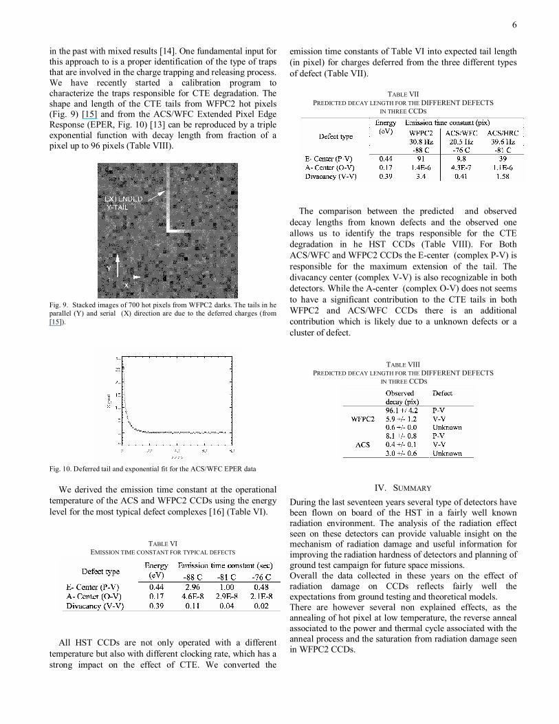
in the past with mixed results [14]. One fundamental input for this approach to is a proper identification of the type of traps that are involved in the charge trapping and releasing process. We have recently started a calibration program to characterize the traps responsible for CTE degradation. The shape and length of the CTE tails from WFPC2 hot pixels (Fig. 9) [15] and from the ACS/WFC Extended Pixel Edge Response (EPER, Fig. 10) [13] can be reproduced by a triple exponential function with decay length from fraction of a pixel up to 96 pixels (Table VIII).
Fig. 9. Stacked images of 700 hot pixels from WFPC2 darks. The tails in he parallel (Y) and serial (X) direction are due to the deferred charges (from [15]).
Fig. 10. Deferred tail and exponential fit for the ACS/WFC EPER data
We derived the emission time constant at the operational
temperature of the ACS and WFPC2 CCDs using the energy level for the most typical defect complexes [16] (Table VI).
TABLE VI EMISSION TIME CONSTANT FOR TYPICAL DEFECTS
All HST CCDs are not only operated with a different
temperature but also with different clocking rate, which has a strong impact on the effect of CTE. We converted the
emission time constants of Table VI into expected tail length (in pixel) for charges deferred from the three different types of defect (Table VII).
TABLE VII
PREDICTED DECAY LENGTH FOR THE DIFFERENT DEFECTS IN THREE CCDS
The comparison between the predicted and observed
decay lengths from known defects and the observed one allows us to identify the traps responsible for the CTE degradation in he HST CCDs (Table VIII). For Both ACS/WFC and WFPC2 CCDs the E-center (complex P-V) is responsible for the maximum extension of the tail. The divacancy center (complex V-V) is also recognizable in both detectors. While the A-center (complex O-V) does not seems to have a significant contribution to the CTE tails in both WFPC2 and ACS/WFC CCDs there is an additional contribution which is likely due to a unknown defects or a cluster of defect.
TABLE VIII PREDICTED DECAY LENGTH FOR THE DIFFERENT DEFECTS
IN THREE CCDS
IV. SUMMARY During the last seventeen years several type of detectors have been flown on board of the HST in a fairly well known radiation environment. The analysis of the radiation effect seen on these detectors can provide valuable insight on the mechanism of radiation damage and useful information for improving the radiation hardness of detectors and planning of ground test campaign for future space missions. Overall the data collected in these years on the effect of radiation damage on CCDs reflects fairly well the expectations from ground testing and theoretical models. There are however several non explained effects, as the annealing of hot pixel at low temperature, the reverse anneal associated to the power and thermal cycle associated with the anneal process and the saturation from radiation damage seen in WFPC2 CCDs.

7
V. REFERENCES [1] M. R. Jones, “ACD WFC CCD Radiation Test: The Radiation
Environment”, ACS Instrument Science Report 00-09, STScI Baltimore, 2000.
[2] J. C. Pickel, A. H. Kalma, G. R. Hopkinson, and C. J. Marshall, 2003, IEEE Trans. Nucl. Sci. vol 50, 671.
[3] Srour, J.R., Marshall, C.J., and Marshall, P.W. 2003, IEEE Trans. Nucl. Sci. vol 50, 653.
[4] Clampin et al. 2005 [5] J. R. Srour, “Basic Mechanisms of radiation effects on electronic
materials, devices, and integrated circuits” Tutorial Short Course IEEE 1982 Nuclear and Space Radiation Effect Conference.1982.
[6] J. Bogaerts, B. Diericks, and R. Mertens, “Enhanced Dark Current Generation in Proton-Irradiate CMOS Active Pixels Sensors”, IEEE Trans. Nuc. Sci. Vol 49, 1513, 2002.
[7] T. M. Brown STIS Instrument Science Report 01-03, STScI Baltimore, 2001.
[8] J. A. Biretta et al., 2006, WFPC2 Instrument Handbook, Version 9.2 (Baltimore: STScI)
[9] J. Mack, et al. , “WFPC2 Dark Current vs. Time”, WFPC2 Instrument Science Report 01-05, STScI Baltimore, 2001.
[10] C. J. Dale, P. W. Marshall, and Burke, E.A., IEEE Trans Nucl. Sci. vol 37, 1784, 1990.
[11] G. R. Hopkinson, C. J. Dale, and P.W. Marshall, IEEE Trans Nucl. Sci. vol 43, 614, 1996.
[12] M. Sirianni, M. Mutchler, and R. Lucas, “Hot Pixel Growth in ACS CCDs”, 2005 HST Calibration Workshop, Ed. A. Koekemoer, P. Goudfrooij, and L. Dressel, (Baltimore: STScI).
[13] M. Mutchler, and M. Sirianni, “Internal Monitoring of ACS Charge Transfer Efficiency”, ACS Instrument Science Report 05-03, STScI Baltimore, 2005.
[14] P. Bristow, “Application of Model Derived Charge Transfer Inefficiency Corrections to STIS Photometric CCD Data”, ST-ECF Instrument Science Report, CE-STIS 2003-001, 2003
[15] J. A. Biretta, V. Kozhurina-Platais, “Hot pixels as a probe of WFPC2 CTE Effects” WFPC2 Instrument Science Report 05-01, STScI Baltimore, 2005.
[16] J. H. Stein, in “Radiation effects in semiconductors”, eds. J.W. Corbett, and G. D. Watkins, 1971.