Noise Characterization of Silicon Strip Detectors - CERN
138
CERN-THESIS-2007-178
-
Upload
khangminh22 -
Category
Documents
-
view
2 -
download
0
Transcript of Noise Characterization of Silicon Strip Detectors - CERN

CER
N-T
HES
IS-2
007-
178

UNIVERSITA DEGLI STUDI DI TRIESTE
DOTTORATO DI RICERCA IN FISICAXX CICLO
Noise Characterization
of Silicon Strip Detectors
Comparison of Sensors
with and without
Integrated JFET Source-Follower
Settore scientifico-disciplinare:FISICA NUCLEARE E SUBNUCLEARE
DottorandoGabriele Giacomini Coordinatore del collegio docenti:
prof. Gaetano Senatore
Tutore e Relatore:
prof. Luciano Bosisio


Contents
Riassunto iii
Abstract iv
Introduction 1
1 Static Characterization of Silicon Microstrip Detectors 3
1.1 ALICE Microstrip Sensors . . . . . . . . . . . . . . . . . . . . . . . 3
1.1.1 Sensor Design and Specifications . . . . . . . . . . . . . . . 4
1.1.2 Acceptance Testing of Sensors . . . . . . . . . . . . . . . . . 6
1.1.3 Punch-Through I-V Characteristic . . . . . . . . . . . . . . 7
1.1.4 Capacitance measurements . . . . . . . . . . . . . . . . . . 8
1.1.5 3D Numerical Device Simulations . . . . . . . . . . . . . . . 21
1.2 Microtrip Sensors with Integrated Source Follower . . . . . . . . . 24
1.2.1 Device Description . . . . . . . . . . . . . . . . . . . . . . . 25
1.2.2 DC Measurements . . . . . . . . . . . . . . . . . . . . . . . 29
1.2.3 AC measurements . . . . . . . . . . . . . . . . . . . . . . . 33
2 Models for Noise Analysis in Silicon Detectors 35
2.1 Noise Sources in Detector Systems . . . . . . . . . . . . . . . . . . 35
2.1.1 Shot Noise . . . . . . . . . . . . . . . . . . . . . . . . . . . 37
2.1.2 Thermal Noise . . . . . . . . . . . . . . . . . . . . . . . . . 38
2.1.3 1f noise . . . . . . . . . . . . . . . . . . . . . . . . . . . . . 39
2.1.4 Noise in JFETs . . . . . . . . . . . . . . . . . . . . . . . . . 39
2.2 Charge Sensitive Amplifier Configuration . . . . . . . . . . . . . . 40
2.3 Source Follower Configuration . . . . . . . . . . . . . . . . . . . . . 44
2.4 Theoretical comparison of CSA and SF . . . . . . . . . . . . . . . 51
2.5 Technological consideration . . . . . . . . . . . . . . . . . . . . . . 52
3 Experimental Set-up for Noise Measurements 55
3.1 Detector Assembly . . . . . . . . . . . . . . . . . . . . . . . . . . . 55
3.2 Preamplifier . . . . . . . . . . . . . . . . . . . . . . . . . . . . . . . 55
3.3 Shaping and Acquisition System . . . . . . . . . . . . . . . . . . . 57
3.4 Signal Generation and Gain Calibration . . . . . . . . . . . . . . . 59
3.5 DC Voltage and Current Supplies . . . . . . . . . . . . . . . . . . . 63
3.6 Calibration of Photogenerated Current . . . . . . . . . . . . . . . . 64
i

4 Noise Measurements on Microstrip Detectors read out by a Charge
Sensitive Amplifier 67
4.1 Noise parameterization . . . . . . . . . . . . . . . . . . . . . . . . . 674.2 Preliminary measurements on a PhotoDiode . . . . . . . . . . . . . 68
4.2.1 DC-coupled measurements . . . . . . . . . . . . . . . . . . . 684.2.2 AC-coupled measurements . . . . . . . . . . . . . . . . . . . 70
4.3 Noise in Strip Detectors . . . . . . . . . . . . . . . . . . . . . . . . 714.4 Unexpected noise components in strip detectors . . . . . . . . . . . 77
4.4.1 Noise due to resistive layers at the surface . . . . . . . . . . 774.4.2 Excess Punch-Through Noise . . . . . . . . . . . . . . . . . 85
5 Noise Measurements on Microstrips with integrated Source-Follower
structure 91
5.1 Modified theoretical analysis . . . . . . . . . . . . . . . . . . . . . 915.1.1 Signal . . . . . . . . . . . . . . . . . . . . . . . . . . . . . . 925.1.2 Noise . . . . . . . . . . . . . . . . . . . . . . . . . . . . . . 94
5.2 Noise on integrated JFETs . . . . . . . . . . . . . . . . . . . . . . 955.3 Measurements on Pixels . . . . . . . . . . . . . . . . . . . . . . . . 965.4 Measurements on Strip Detectors . . . . . . . . . . . . . . . . . . . 99
5.4.1 CSA Readout . . . . . . . . . . . . . . . . . . . . . . . . . . 995.4.2 Readout with Source-Follower . . . . . . . . . . . . . . . . . 102
6 Comparative Discussion of the Experimental results on CSA and
SF 109
6.1 Pixels . . . . . . . . . . . . . . . . . . . . . . . . . . . . . . . . . . 1116.2 Strip . . . . . . . . . . . . . . . . . . . . . . . . . . . . . . . . . . . 112
Conclusions 114
A Instruments for static characterization of devices 117
B 241Am spectra 121
Bibliography 129

Caratterizzazione del rumore
in rivelatori a microstriscia su silicio
Confronto tra sensori
con e senza
inseguitore di source a JFET integrato
Riassunto
Il rumore e spesso il principale fattore che limita le prestazioni di un sistemadi rivelazione. In questo lavoro si riporta un dettagliato studio dei contributi dirumore in diversi tipi di sensori al silicio a microstriscia.
Si sono investigati sia sensori con lettura a doppia faccia, fabbricati da tredifferenti fornitori per l’esperimento ALICE presso lo LHC del CERN, sia rivelatoriche includono, come primo stadio di condizionamento del segnale, un “Source-Follower” a JFET, integrato sullo stesso substrato del sensore. Questi ultimi sonostati progettati nel tentativo di migliorare le prestazioni del sistema quando sonorichieste strisce molto lunghe, ottenute concatenando insieme vari sensori.
Dopo una descrizione dei sensori a microstriscia utilizzati, vengono illustratee interpretate le misure di caratterizzazione statica eseguite su di essi (corrente ecapacita verso tensione e/o frequenza). Come aiuto nell’interpretazione di alcunepeculiari caratteristiche di queste misure si e fatto ricorso a simulazioni numerichedel dispositivo.
Sono poi descritti i modelli comunemente usati per esprimere il rumore del sis-tema rivelatore-amplificatore in funzione dei parametri che lo caratterizzano. Sonostate considerate e confrontate due configurazioni del primo stadio di trattamentodel segnale: il tradizionale amplificatore di carica e l’inseguitore di “source”.
Segue la descrizione delle misure di rumore eseguite e dei relativi risultati. Sonostate misurate curve della carica equivalente di rumore in ingresso, in funzione deltempo di picco del formatore, per diversi valori della corrente di buio. Quest’ultimae stata variata per fotogenerazione (illuminando il sensore con un LED) o, inalternativa, iniettandola direttamente nella striscia sotto esame per mezzo di unasorgente esterna di corrente (attraverso una resistenza di alto valore).In tal modo e stato possibile verificare i modelli per il rumore su un ampio intervallodei parametri, ed evidenziare chiaramente il contributo di rumore del meccanismodi punch-through, utilizzato per polarizzare le strisce.
Il rumore misurato con lettura del segnale tramite amplificatore di carica egeneralmente in buon accordo con il modello comunemente usato, ma in qualchecondizione operativa si sono trovati contributi inaspettati. Questi sono stati inter-pretati correlandoli con alcune caratteristiche particolari delle misure di capacita.Il rumore misurato sui rivelatori con Source-Follower integrato e in accordo con lepredizioni del modello, quando per i parametri si usano i valori misurati.
Infine si confrontano le prestazioni dei due differenti approcci per la lettura delsegnale.
iii

Abstract
Noise is often the main factor limiting the performance of detector systems. Inthis work a detailed study of the noise contributions in different types of siliconmicrostrip sensors is carried on. We investigate three sensors with double-sidedreadout fabricated by different suppliers for the ALICE experiment at the CERNLHC, in addition to detectors including an integrated JFET Source-Follower asa first signal conditioning stage. The latter have been designed as an attempt atimproving the performance when very long strips, obtained by gangling togetherseveral sensors, are required. After a description of the strip sensors and of theiroperation, the “static” characterization measurements performed on them (currentand capacitance versus voltage and/or frequency) are illustrated and interpreted.Numerical device simulation has been employed as an aid in interpreting someof the measurement results. The commonly used models for expressing the noiseof the detector-amplifier system in terms of its relevant parameters are then pre-sented. Two configurations of the first signal processing stage are considered andconfronted: the usual charge-sensitive amplifier and the Source-Follower. Next,the noise measurements performed and their results are illustrated. Curves of theequivalent input noise charge versus shaping time of the filtering amplifier, forseveral values of the leakage current, have been obtained. The leakage currenthas been varied by photogeneration, illuminating the sensor with a LED, or alter-natively by injecting it into the strip from an external current source, through ahigh-value resistor. The noise measured with the strip sensors read-out by a charge-sensitive amplifier generally agrees well with the common model, but in some oper-ating conditions unexpected contributions have been found. These have been inter-preted by correlating them with some peculiar features of the capacitance-voltagemeasurements. The noise measured on the detectors with integrated JFET source-follower complies with the prediction of the model, using the measured values ofthe relevant parameters. Finally, the performances of the two different approachesare confronted.
iv

Introduction
Since the pioneering work of Josef Kemmer on the fabrication of silicon de-tectors with the planar process [1], much progress has been made. Advancementsin both detector and IC technologies opened the way to a varied array of siliconsensors, for many applications, in both science and industry. The power, flexibilityand reliability of the technology allowed the introduction of various new kinds ofdetectors.Among the first and most straightforward ones are strip detectors, in which thejunction electrodes are shaped as long, narrow, parallel strips, allowing to de-termine with high spatial accuracy the coordinate orthogonal to the strip of theimpact point of a detected particle.Strip detectors have become a fundamental part of the inner tracking system ofmost high energy physics experiments. Because of their geometry, they cannot de-termine completely the position of the ionizing event, lacking information about thecoordinate parallel to the strip. So, a signal from a further sensors, e.g. with stripsat a different angle, is needed for a complete position determination. Anyway, theyallow high spatial resolution, with a reduced number of read-out channels, com-pared with real 3D tracking devices as pixels. Strip detectors are commonly readout by Charge Sensitive Amplifiers (CSA), integrated into custom VLSI chips to-gether with further amplification, shaping and a variety of other optional functionssuch as analog sample and hold with multiplexed read-out, ADC conversion, trig-gering, and more.These chips are usually not commercial but are designed by the experiment teamand fabricated by a foundry. The read-out chip is mounted as close as possibleto the strips, in order to minimize stray connection capacitance. Every channel ofthe chip is bonded to a strip.The advantage of the CSA configuration is that, as will be explained, the signal isindependent on the parameters of the detector; it depends only on the well definedfeedback capacitance. The detector capacitance, strip series resistance and leakagecurrent affect only the level of noise.For long strips, with a large capacitance, the option could be considered of sub-dividing the strip into shorter ones, individually connected to a simple first signalprocessing stage, integrated on the detector itself. Then, by means of thin cables,the signal is brought outside the tracking region, for further processing. An inte-grated Source Follower is a natural choice for this approach, since it has low outputimpedance, able to drive high capacitive loads, as presented by the long connec-tions to the outer stages. A suitable fabrication technology had been developedat ITC-irst 1 (Trento) for the integration of n-channel JFETs on high resistivitysilicon substrates, together with p-i-n detectors. The good static and dynamiccharacteristics of these JFETs had been demonstrated, but their suitability forthe read-out of strip detectors had not yet been investigated.One aim of this thesis, then, is to verify this point and, in particular, if it couldgive better noise performances with respect to a standard CSA read-out.In chapter 1, the static characterization of the devices used throughout this workis presented. Two kind of strip detectors are considered: those designed for theITS (Inner Tracking System) of the ALICE experiment at CERN and strips with
1Now, “FBK - irst”.
1

integrated Source-Follower, developed under a “PRIN 2003” project. In the INFN-Trieste laboratory, the characterization and the quality acceptance tests of allmicrostrip detectors for the ALICE experiment have been made. On similar de-vices, we performed some additional tests; in particular, capacitance measurementsopened the way to interpreting some peculiar features of the noise measurements.On detectors with SF, a characterization of the JFETs, constituting the source-follower stage, determined their parameters to be used in noise considerations.In chapter 2, the noise as a physical quantity is introduced and the basic ideasof signal processing and noise analysis are presented for both the CSA and theSF configurations. Making some approximations, we derived the conditions fordetermining when one configuration is expected to be better than the other.In chapter 3, the experimental set-up is described. The characteristics of the com-mercial single channel preamplification and filtering-shaping chain are presented,followed by the methods employed to generate signals with a conveniently highrate, as needed for an efficient noise determination.Chapter 4 deals with noise measurements with the CSA read-out configuration.In order to fully characterize the signal processing, measurements with a simplediode detector have been made first. The measurements are based on noise scansversus peaking time, facilitated by the fact that the digital shaper allows selectingthe shaping parameters within a wide range. Leakage and punch-through currentsare varied too, checking their noise contributions. The same measurements arethen performed on the strip detector, employing different methods for the polar-ization of the strips and investigating both sides of the detector (p and n strips).On these devices, the dependence on the bias voltage has been studied, leading tosome unexpected results. These effects have been related to some features of thecapacitance measurements described in chapter 1. A comparison with excess noiseterms, found but not explained by other groups, is carried on.Chapter 5 reports the noise scans made on structures with integrated SF. Forthese devices our set-up was not suitable to process the signals in an optimal way;however, we derived analytical expressions for both the signal and the noise underthese conditions. As a result, signal and noise are discussed separately while theENC, used in the CSA case, is not taken into account, since it does not give addi-tional information. First pixels (devices with very extremely small area) and thenstrips are studied. A comparison with the theory discussed in chapter 2 is made.Finally, in chapter 6, the experimental data are commented in the light of the the-oretical expectations described in chapter 2, to answer the question that startedour investigation:
SF or CSA?
2

Chapter 1
Static Characterization of
Silicon Microstrip Detectors
1.1 ALICE Microstrip Sensors
The ALICE experiment at the Large Hadron Collider at CERN is designed forthe detection of events generated by heavy ion collisions. In order to cope withthe very high multiplicity of these events, the inner part of the tracking system iscomposed of six layers of silicon detectors with finely subdivided readout [2] [3].The two outer layers, placed at average radii of 39 and 44 cm, are made up of stripdetectors.
Given the low interaction rate during ion beam operation of the LHC andthe relatively large radius of the strip layers, the expected radiation levels for10 years of operation are very modest: a dose of 40 Gy and a hadron fluence of4·1011 cm−2 [3]. Such values do not pose demanding requirements on the radiationtolerance of the microstrip sensors.
The need for minimizing the material thickness forced the choice of double-sided sensors, while integrated AC-coupling capacitors are required for reliableoperation of the detector system and simplification of the assembly process. Thehigh expected track density (about 1 cm−2) led to the adoption of a small-anglestereo geometry for the strips on opposite sides of the sensor, in order to limit theoccurrence of ambiguities in track reconstruction.
The two strip layers are composed of 1698 sensors of a single type, for a to-tal sensitive area of ∼5 m2. The sensors have been provided by three differentsuppliers:
- Canberra Semiconductor NV, Lammerdries 25, B-2250 Olen, Belgium
- ITC-irst (now FBK-irst), Via Sommarive 18, I-38050 Trento, Italy
- SINTEF Electronics and Cybernetics, Blindern, N-0314 Oslo, Norway
All measurements reported in this work concerning the ALICE microstrip de-tectors have been performed on four test detectors (identical to the main onesexcept for a reduced number of strips, as described in Section 1.1.1). These willbe referred to by the following abbreviations:
- AI , indicating a test sensor fabricated by ITC-irst.
3

- AE , indicating a test sensor fabricated by Canberra.
- AS1,AS2 indicating two test sensors fabricated by SINTEF. Of these, AS2has been irradiated with low energy X-rays (20 keV), illuminating the p-side,to a dose of ∼130 Gy, to the purpose of increasing the positive oxide chargeand prevent inversion of the interface [4].
1.1.1 Sensor Design and Specifications
The sensor has an overall size of 75 mm × 42 mm and a standard thickness of300 µm [5]. The chosen stereo angle of 35 mrad between the two sides results fromp-side strips forming an angle of +7.5 mrad with the short edge of the sensor andn-side strips forming a corresponding angle of -27.5 mrad.
The strips are about 40 mm long and placed at a pitch of 95 µm. At each endof a strip there are two bonding/probing pads on the upper (metal) electrode ofthe integrated capacitor (“AC pads”), and one smaller probing pad (“DC pad”)connected to the lower electrode (implanted or diffused strip in the silicon sub-strate). The AC pad layout has reflection symmetry about the two detector axesand is identical on p and n sides, thus simplifying both testing and assembly.
On p-side, the strips are biased by punch-through from a surrounding biasring [6] [7] [8]. Confronted with polysilicon resistors, this method of biasing is sim-pler to implement (no need for additional processing) and does not take room onthe sensor layout. Furthermore, it avoids the thermal noise associated with a biasresistor, although it brings its own specific noise contributions, which are discussedin Sections 4.3 and 4.4.2. The main drawback of punch-through biasing is limitedradiation tolerance, but this is not a concern for the ALICE strip detectors, giventhe very modest radiation levels they are expected to face.A similar scheme has been adopted on n-side, where the strips are biased by in-jection of electrons toward the bias ring, across a potential barrier created by theinsulation structure (p-stop or p-spray, depending on the supplier’s choice).A microscope picture of a corner on the n-side of the AI sensor is shown in Fig-ure 1.1.
Outside of the bias ring, a guard ring is present and, on p-side, a number offloating rings are implemented in order to control the peak electric fields. Theguard ring design and the details of strip design at the silicon level are defined bythe suppliers of the sensors.
On the wafer, alongside the main detector, there is ample space for test struc-tures. In addition to the standard devices for measuring properties of the substratematerial and parameters of the fabrication process, a test detector has been in-cluded.
The test sensor is identical to the main one in all details of both the strips andthe edge regions (bias rings, guard rings, scribe lines), the only difference being areduced number of strips: 128 instead of 768. As a consequence, the overall sizeof the sensor is reduced to 14.2 mm × 42 mm. The small-angle stereo geometryallows designing a smaller detector with the same strip length of the large one, onboth sides.
Because of the identical design, all properties of the sensors can be investigatedon the test detectors, with obvious advantages in terms of availability (they are notneeded for installation in the ALICE tracker) and a more compact size, facilitating
4

Figure 1.1: Microscope picture of a corner on the n-side of the AI sensor. Thep-stop implants surrounding the n-type strips are clearly visible.
assembly and bonding.
According to the electrical specifications, a strip is classified as defective ifeither of the following happens [5]:
- the leakage current of the DC strip exceeds 20 nA;
- the effective insulation resistance of the DC strip is below 50 MΩ;
- the AC capacitor is broken;
- the metal AC strip is shorted to adjacent ones or to bias ring (“metal short”);
- the metal AC strip is interrupted (“metal open”).
The acceptance criterion requires the total number of defective strips on the twosides of a sensor to be less than 30, corresponding to about 2% of all strips.The sensor must also comply with specifications on the maximum detector op-erating voltage, maximum total current and on the current stability in time. Inaddition, there are specifications on the values of the interstrip capacitance, theAC coupling capacitance, the metal strip resistance, the punch-through voltagedrop and the differential punch-through resistance. These parameters are testedonly on a sampling basis [5], since they are not related to random defects, butrather to design and processing aspects.
5

1.1.2 Acceptance Testing of Sensors
The acceptance testing and quality control of the microstrip sensors for the ALICEInner Tracking System has been performed at the Trieste INFN laboratory.
A detailed description of the testing procedures adopted can be found in [5]and a summary of test results is given in [9]. Here we only recall the main stepsof the routine acceptance test, performed on every sensor.The n-side of the sensor is tested first, with the following sequence:
1) AC Strip Scan: Every strip capacitor is measured sequentially, with 20 Vbias applied across it. Capacitance, dissipation factor and leakage currentare measured simultaneously.
2) I-V Measurement: The currents of bias and guard rings on p-side (back-side) are measured, together with the current of one n-side strip, with thebias voltage reaching up to 100 V. The strip I-V characteristic allows a quickestimate of the insulation bias voltage, since parasitic currents due to instru-ment offset voltages dominate the measured strip current until good stripinsulation is reached.
3) Punch-Through V oltage Measurement: The punch-through voltage dropbetween bias ring and strip is measured versus bias voltage, for two differentstrips.
4) DC Strip Scan: Leakage current and insulation resistance of every strip aremeasured.
Tests 1), 3) and 4) are then repeated on p-side (there is no need to redo theI-V measurement). The time required for the complete characterization of one(full-size) sensor is normally about two hours.
In the following we will be concerned only with measurements made on the fourtest sensors mentioned above, to the purpose of characterizing their properties inview of the noise measurements.First, good quality sensors have been selected by performing the standard accep-tance measurements.The AI detector showed a low depletion voltage1 of ∼15 V. The AE detectorshowed an even lower depletion voltage of just ∼8 V, while the AS detectors havehigher depletion voltages, around 40 V.
After cutting from the wafer, the sensors have been glued upon fiberglass sup-ports and bonded on both sides to gold-plated copper traces.The assembly provides external access to:
- on each side, the bias ring and the guard ring;
- one (centrally located)strip per side; bonding provides independent access toits DC and AC pads;
- on each side, the AC pads of all the other strips, bonded together to acommon line.
1the “depletion voltage” is defined here as the minimum bias voltage at which every n-sidestrip is insulated from the others, with an effective interstrip resistance exceeding 100 MΩ.
6

0 1 2 3 4
-10n
-5n
0
5n
I stri
p (A
)
V strip (V)
Figure 1.2: Punch-through I-V characteristic: while all others strips sit at theirpunch-trough voltage, the voltage of the single bonded strip is varied. Above acertain threshold (∼3 V in this figure) a nearly exponential punch-through currentstarts flowing from the strip to the bias ring.
We describe in the following subsections a few additional measurements, notroutinely made on the ALICE sensors, with particular attention to capacitancemeasurements, which are important for interpreting the noise data.
1.1.3 Punch-Through I-V Characteristic
During the standard acceptance tests, the punch-through voltage of a few samplestrips has been measured versus the detector bias voltage. This measurement isperformed by contacting the DC pad of the strip and reading out the voltagewith a very high impedance “voltmeter” (an SMU channel of the HP4156A set incurrent-mode, at zero current).
To get more insight on the punch-through mechanism we can measure its I-Vcharacteristic, for a given value of the bias voltage. This is done by varying thevoltage applied to the DC pad of the strip, and measuring the current flowing intothe DC pad itself from the external instrument (SMU channel in voltage-mode:forces voltage, measures current). The punch-through current, flowing from thestrip to the bias ring, is then the sum of the leakage current with the externallymeasured current.
Figure 1.2 shows an example of such a measurement, for a p-side strip of sensorAS2 (the leakage current is higher than normal because of the surface generationcaused by the X-ray irradiation). When the strip is at 0 V (the same voltage asthe bias ring), it collects more than its “fair” share of leakage current, since theadjacent strips are at punch-through voltage (a few volt positive); this causes adeformation of the electric field in the silicon, with more field lines reaching the
7

strip, which then collects also a fraction of the leakage current normally flowingto the neighbouring strips. No punch-through current flows between the strip andthe bias ring, because they are at the same voltage, hence the leakage currentflows to the external instrument (reading a negative current because of the signconvention).When a positive voltage is applied to the strip, the voltage difference with theadjacent ones is reduced, and the collected leakage current decreases (in absolutevalue): this is shown by the (almost linear) slope of the first part of the plot.Finally, when the strip voltage becomes large enough to cause a significant punch-through current to the bias ring (∼3 V in this case), the current measured by theinstrument quickly goes to zero (the condition in which all the strip leakage cur-rent flows by punch-through), then reverses sign and grows with an approximatelyexponential dependence on the strip voltage.At “large” current values (depending on geometry and substrate doping, about10 nA are enough in this case) the punch-through current significantly devi-ates from the exponential behaviour, to become space-charge limited when thecarrier density in the punch-through region becomes comparable with the sub-strate dopant density. The current then exhibits a power-law dependence on volt-age [7] [10].
If one needs an accurate measure of the strip leakage current in its “normal”operating conditions (when it is biased by punch-through), the best procedurewould be to extrapolate the linear part of the plot in Figure 1.2 to the punch-through voltage (the voltage at which zero current is measured).
1.1.4 Capacitance measurements
The only capacitances routinely measured on ALICE strip detectors are those ofthe integrated AC coupling capacitors, made up of a thin layer of SiO2 betweenthe implant and the metal. On a sampling basis, interstrip capacitances to firstand second neighbors have also been measured [5]. For this work, a few moredetailed measurements have been performed, taking advantage of the wire-bondedconnections to the strips and bias ring on both sides of the sensors. In the followingwe illustrate, among these measurements, those that are most relevant for theinterpretation of the noise characteristics of the sensors. The equipment and theprocedures used for capacitance measurements are briefly described in Appendix A.
In the measurements, connections to the strip are made to the AC pads (i.e.to the metal strips) rather than the DC ones (i.e. to the implanted strips). Onthe one hand, the capacitances to be measured are at most on the order of 10 pFper strip, at least an order of magnitude less than the coupling capacitance, sothat the difference in the measurement results introduced by adding the couplingcapacitance in series is small. More importantly, it is actually the capacitancesmeasured on AC pads that affect the performance characteristics of the detectorreadout (such as noise), because the front-end electronics is connected to the ACpads.
One of the most important detector parameters entering in noise calculationsis the total capacitance between the charge collecting electrode (e.g. a strip) andall other electrodes that are kept at fixed voltage, i.e. at ground for what concernsthe signal [11]. This can be measured, for example, by feeding the sinusoidal small-signal voltage vAC (see Appendix A) to all the other electrodes and measuring the
8

induced AC current on the strip under study. It is instructive, however, to considerseparately the various capacitances between the strip and the other electrodes.
Unless otherwise stated, the capacitance-voltage measurements (C-V charac-teristics) reported in the following are performed at 200 kHz frequency. This ap-proximately corresponds to the shaping times (a few µs) used in the noise measure-ments; furthermore, the measured values do not significantly depend on frequencyin a large interval around this point. Special features of the frequency-dependenceof capacitance and dissipation factor are then investigated with measurementsperformed versus frequency (C-f characteristics), for different values of the biasvoltage.
Consider first the capacitance between a strip and the opposite side (backside)of the sensor. Because the AC pads of all strips are wire bonded to just a fewterminals, in our setup it is easy to measure the capacitance between all p-sidestrips and all n-side ones. Dividing the result by the number of strips we get afairly accurate measurement of the capacitance between a single strip and all theothers on the opposite side, i.e. the backside capacitance of a strip. Figure 1.3reports the capacitance between all the p-side and all the n-side strips, measuredversus bias voltage, for sensor AS1. The backside capacitance is plotted as C−2
(as is common practice) because for one-dimensional one-sided junctions the slopeof the C−2 − V plot is inversely proportional to the doping concentration [12]; fora uniformly doped substrate we then get a linear increase until the total depletionvoltage is reached and the curve flattens out. In our case we expect deviationsfrom the simple linear plot, because of two reasons: first, the junction is composedof many strips, so the geometry is not one-dimensional, and in addition there areinterface charges in the interstrip gaps, altering the electrostatics of the problem;second, the actual bias voltage between p-side and n-side strips differs from theapplied voltage because of the (non constant) punch-through voltage drops on bothsides. Nevertheless, we observe that the plot in Figure 1.3 is still approximatelylinear. From the knee of the curve we can estimate that total depletion of thesubstrate is reached at a voltage of 41 V applied between the two bias rings (thisincludes the punch-through voltage drops).
For strip pitches smaller than the substrate thickness, the major contributionto the total capacitance of a strip usually comes from the interstrip capacitance,which is dominated by the capacitance to first neighbours. With our set-up, wecan easily measure the capacitance of one strip towards all other strips on the sameside. Figure 1.4 shows the interstrip capacitance versus bias voltage, measured onsensor AS1. In order to measure only the interstrip capacitance, the bias ring andthe backside must be kept at signal ground. The figure also shows the capacitancemeasured when the backside is made floating for the AC signal, which has beenobtained by supplying the bias voltage through a 1 MΩ resistor. In this latter case,the backside (including the undepleted part of the substrate at low bias voltages) iscoupled to the AC signal by the backside capacitance of the n-1 strips connected tothe HIGH terminal; in turn the backside is coupled to the strip under measure bythe backside capacitance of that strip. It follows that the backside almost exactlyfollows the vAC signal, so that we measure the sum of the interstrip and the strip-to-back capacitance. As a consequence, the measured capacitance increases at lowbias voltages, where the capacitance to backside becomes important. Conversely,when the backside is grounded for the signal, the capacitance decreases at lowbias voltage, because of the partial screening of the interstrip capacitance by the
9

0 10 20 30 40 50 60 70 800
1x10¹⁹
2x10¹⁹
3x10¹⁹
4x10¹⁹
C
p-2 (F
-2)
V back (V)
Figure 1.3: Detector AS1. Capacitance between all the p-side and all the n-sidestrips, measured as a function of the voltage applied between the two bias rings.The function C−2 is plotted.
undepleted bulk.
In order to measure the total capacitance of a (metal) strip towards all otherelectrodes, we connect the AC pad of a single strip to the LOW terminal, while thebias ring and the AC pads of all other strips on the same side are connected to theHIGH terminal. The bias ring and all AC pads on the opposite side are connectedto HIGH through a large capacitor and to the bias voltage supply through a 1 MΩresistor. Since the current flowing through the resistor is small (tens of nA), thecorresponding voltage drop is negligible compared to the reverse bias voltage. Inany case, it could be easily corrected for by measuring the bias supply current andsubtracting the IR product from the applied voltage.This configuration – with the metal strips at the same DC voltage of the cor-responding bias ring, and the underlying implanted strips at their appropriatepunch-through voltage – is the one applying during normal operation of the detec-tor, when each strip is connected to a preamplifier, and the front-end electronicsis floated at the detector bias voltage. An example of the measurement of thiscapacitance versus bias voltage is given in Figure 1.5, relative to an n-side stripof sensor AS1. The sharp increase of the measured capacitance and dissipationfactor below 40 V reflects the fact that the n-side strips are not insulated belowthis voltage. Above the strip insulation voltage, the capacitance slowly decreasesbecause of a slight lateral depletion of the electron accumulation channels presentin between the p-stop implants that are used to insulate the strips.
The values of total strip capacitance and dissipation factor measured at 60 Vbias for all four sensors are summarized in Table 1.1. The depletion voltages ofthe sensors are also indicated. The quoted C and D values refer to the particularstrips (one per side on each sensor) that have been individually bonded to an
10

0 20 40 60 80 1000
2p
4p
6p
8p
10p
12p
14p
Cp
(F)
V back (V)
back floating back grounded
Figure 1.4: Detector AS1. Capacitance between one p-side AC strip and all theothers ones, versus bias voltage. The figure shows curves obtained with the back-side grounded or floating for the AC signal. f = 200kHz
0 20 40 60 80 1000
5p
10p
15p
20p
D C
V bias (V)
C (F
)
0.00
0.01
0.02
0.03
0.04
0.05
D
Figure 1.5: Total capacitance and dissipation factor for a single n-side strip of sen-sor AS1. It includes the capacitance toward the backside, the bias ring (negligible)and all others strips on the same side. f = 200 kHz
11

Capacitance Capacitance Vdepl
p-side (pF) n-side (pF) (V)
CANBERRA AE 10.2 (0.6 %) 12.2 (4.6 %) 8
ITC AI 10.6 (0.6 %) 10.3 (1.0 %) 15
SINTEF AS1 6.8 (0.7 %) 8.8 (3.4 %) 42SINTEF irr. AS2 6.8 (1.3 %) 8.3 (4.1 %) 40
Table 1.1: Total strip capacitance and dissipation factor (in parentheses) for thesensors studied, measured at 60 V bias and 200 kHz frequency. The depletionvoltages of the sensors are also indicated. Sensor AS2 has been irradiated with20 keV X-rays illuminating the p-side, at a dose of 130 Gy
external terminal. The same strips are used for the noise measurements, so thatvalues reported can be appropriately used in models for noise analysis. However,the strip capacitance is subject to variations inside the same sensor and, to a largerextent, between sensors coming from different wafers and/or production lots. Forthis reason, when confronting different types of sensors the quoted capacitancescan be taken as significant only with an uncertainty of 10%.We observe that the n-side strips have larger capacitance than p-side ones, withthe exception of the AI sensor, for which there is no difference. Furthermore, theirradiation with X-rays does not seem to have appreciably changed the capacitanceof the AS sensors.
The dissipation factor is comfortably low (< 5%), at least when depletion isreached, and this ensures that the capacitance is a well-determined parameter. Infact, the relative differences between the values obtained with series and parallelmodels are of order D2.However, the dependence of D on bias voltage, above total depletion, shows char-acteristic features, with some differences between the sensors studied. Figure 1.6reports the measured D vs. Vbias curves of strips, for the AE and AI sensors (theones with low depletion voltage).
On the n-side of detector AE the dissipation factor, after a very steep dropcorresponding to the strip insulation voltage, remains almost constant at a rela-tively high value of 4.5%. The n-side of sensor AI shows a different pattern: afterdropping sharply when the strip becomes insulated ( 16 V), D decreases graduallyuntil, about 40 V above depletion, it suddenly changes to a constant value closeto 1%.On the p-side, there is no sharp drop in D at total depletion, since the p-strips areinsulated from the n-type bulk at all bias voltages (the high value of D at very lowbias, 0-1 V, is likely due to the large strip capacitance to the undepleted, highlyresistive bulk). The p-side plot for the AE sensor shows a behavior similar to then-side of the AI sensor: D smoothly decreases until it suddenly flattens at about50 V bias. This characteristic of the dissipation factor is interesting because, incontrast to it, the capacitance (measured at the same frequency of 200 kHz) showsvery little voltage dependence above total depletion.
These features, due to a resistive component of the admittance, are presum-ably related to surface effects, because after the substrate is depleted, changes inresponse to bias voltage variations can only take place in surface structures andlayers. In fact, the backside capacitance measurements show constant dissipation
12

0 20 40 60 80 1000.00
0.01
0.02
0.03
0.04
0.05
0.06
D
V back (V)
Canberra P - side Canberra N - side ITC N-side ITC P - side
Figure 1.6: Dissipation factor versus bias voltage for p-side and n-side strips ofsensors AE and AI. Notice the depletion voltage of the detector, clearly shown bythe sharp fall of D for n-side strips. f = 200kHz
factors (< 1%) above total depletion, practically independent on frequency.
In order to explain these features, the capacitance and dissipation factor havebeen studied in the frequency domain: a series of measurements versus frequencyhave been carried out, for different values of the bias voltage (above total deple-tion). The results of the measurements have been confronted with the predictionsof a very simple model.In the following subsections the situations for the sensors type AE and AI areconsidered separately.
AE-type sensor
At the surface of the AE detector, both on p and on n-side, the bias ring is sep-arated from the strips and each strip from the others by a layer of opposite con-ductivity: on p-side an electron accumulation layer induced by the positive oxidecharge and on n-side a p-spray layer, a low dose boron implant uniform across thewafer [13]. Then we expect the situation to be similar on the two sides. We ver-ified that the measured interstrip capacitance is insensitive to whether or not thebias ring is connected to ground or to the HIGH terminal; this is true on both sides.
Consider measurements on n-side first, as reported in Figure 1.8. Looking atthe curve for the dissipation factor D, we notice that a function of the type:
D ∝ ωτ
1 + (ωτ)2(1.1)
13

Cis Cis
LOW HIGH
C layer
BR
HIGH
C layer C layer
LOW
R
R
(a) (b)
Figure 1.7: Simplified model of the interstrip impedance applying to: (a) AEsensor and p-side of AI sensor; (b) n-side of AI sensor.
with τ ∼(10 kHz)−1, has a very similar frequency dependence.An impedance made up by a capacitance in parallel with the series combina-
tion of a resistance and a capacitance, as shown in Figure 1.7(a), can account forthis shape.This schematic can be interpreted as follows: Cis is the “direct” interstrip capaci-tance (dominated by first neighbours, with a small contribution from other neigh-bours), Clayer is the capacitance of the strip versus the resistive layer (p-spray onn-side, electron accumulation channels on p-side) in series with the capacitance ofthis layer to all other strips, and R is the resistance of the resistive layer path link-ing the strip to all other strips. Obviously this is an extremely simplified model,with just three lumped elements replacing distributed capacitances and resistancesin electrodes of complex geometry.
With some tedious calculations we obtain the values of D and Cp = Im(Y )/ωfor the simple circuit of Figure 1.7(a):
D =Re(Y )
Im(Y )=
ωR(Clayer − Cis ⊕ Clayer)
1 + (ωR)2(Cis ⊕ Clayer)Clayer(1.2)
Cp =Im(Y )
ω= (Clayer + Cis)
1 + (ωR)2(Cis ⊕ Clayer)Clayer
1 + (ωClayerR)2(1.3)
where the notation Clayer ⊕ Cis stands for the series combination of the two ca-pacitances.
Consider now the p-side of sensor AE, where more interesting features appear.The results of the model of Figure 1.7(a) are compared with the measured C-f
and D-f curves in Figure 1.9. The values of Cis and Clayer (given in the caption)have been adjusted in order to reproduce the capacitance measured at low andhigh bias voltage in the low-frequency limit (when R can be neglected). Once thisis done, the model can qualitatively reproduce the dependence of C and D on thebias voltage by varying the value of the layer resistance R. The flat C and Dcurves measured at high bias voltage (above ∼50 V) are obtained when R → ∞(indeed in Equations 1.2 and 1.3 Cp becomes independent of f and D → 0 whenR → ∞). This is interpreted by assuming that the electron accumulation layeron p-side is interrupted at high bias voltage, suppressing the long-range capacitivecoupling between strips. 3-D device simulations (Section 1.1.5) show that indeedin the narrow (6 µm) punch-through gap at the end of the strips the accumulation
14

layer is depleted due to the punch-through voltage difference between strips andbias ring, thus insulating the interstrip accumulation channels from each other.At lower bias voltages, when the accumulation layer is not interrupted, the lowfrequency capacitance shows the large contribution of the coupling Clayer to theresistive layer, while at high frequency this contribution is cut off by the seriesresistance R.
Going back to the n-side measurements (Figure 1.8), the fact that D is almostindependent on the bias voltage can be related to the fact that the implanted p-spray layer, having a dopant density per unit surface much larger than the densityof the accumulation electrons, is only marginally depleted at its edges, and nevergets interrupted.
It can be seen that the model, despite its gross oversimplification of the realsituation, is able to qualitatively reproduce the main features of the measurements.
15

100 1k 10k 100k 1M0
5p
10p
15p
20p
25p
Cp
(F)
f (Hz)
25 V 40 V 50 V 60 V
(a)
100 1k 10k 100k 1M0.00
0.05
0.10
0.15
0.20
0.25
D
f (Hz)
(b)
Figure 1.8: AE sensor, n-side. (a) Capacitance versus frequency of the single striptowards all other strips on the same side, for four values of the bias voltage (25,40, 50 and 60 V). (b) Dissipation factor for the same measurement.
16

100 1k 10k 100k 1M0
3p
5p
8p
10p
12p
15p
Cp
(F)
f (Hz)
25 V 40 V 50 V 60V
(a)
100 1k 10k 100k 1M-0.05
0.00
0.05
0.10
0.15
0.20
0.25
D
f (Hz)
25 V 40 V 50 V 60 V
(b)
100 1k 10k 100k 1M0.0
2.5p
5.0p
7.5p
10.0p
12.5p
15.0p
Cp
(F)
f (Hz)
R = 10M R = 100M R = 1G
(c)
100 1k 10k 100k 1M0.00
0.05
0.10
0.15
0.20
0.25
0.30
0.35
D
f (Hz)
R = 10M R = 100M R = 1G
(d)
Figure 1.9: AE sensor, p-side. (a) Capacitance versus frequency of the single striptowards all other strips on the same side, for four values of the bias voltage (25, 40,50 and 60 V). (b) Dissipation factor for the same measurement. (c) Capacitancecalculated from the model of Figure 1.7a, with Clayer = 7 pF, Cis = 8 pF andthree values of R (10 MΩ, 100 MΩ, 1 GΩ). (d) Dissipation factor calculated fromthe model, with the same parameter values.
AI-type sensor
On the p-side of the AI sensor (Figure 1.10), the capacitance is independent offrequency for every bias voltage applied, and the dissipation factor is always low(< 1%). According to our previous model, this means that the accumulationchannels in between the strips are not connected to each other at their ends,because the surface region between the bias ring and the strips is depleted even atthe low bias of 25 V. This different situation with respect to the p-side of the AEsensor may be caused by the shorter punch-through gap (5 µm) and by a possiblysmaller positive charge in the oxide.
On n-side, the strip insulation is obtained by surrounding the strips with ap-doped frame, called “p-stop”. In addition, a p-stop strip is laid in between thep-stop frames, so that two adjacent n-side strips are separated by three p-stopimplants (see Figure 1.1).We can represent the situation actually occurring with the aid of the model inFigure 1.7(b), in which an electron accumulation layer between the p-stops is inohmic contact with the n-type bias ring (in contrast to the previously discussed
17

100 1k 10k 100k 1M0
2p
4p
6p
8p
10p
12p
Cp
(F)
f (Hz)
18 V 25 V 50 V 60 V(a)
100 1k 10k 100k 1M0.000
0.005
0.010
D
f (Hz)
25 V 18 V 50 V 60 V
(b)
Figure 1.10: AI sensor, p-side. (a) Capacitance versus frequency of the single striptowards all other strips on the same side, for four values of the bias voltage (18,25, 50 and 60 V). (b) Dissipation factor for the same measurement.
18

100 1k 10k 100k 1M0.0
2.5p
5.0p
7.5p
10.0p
Cp
(F)
f (Hz)
25 V 50 V 60 V
(a)
100 1k 10k 100k 1M
-0.4
-0.3
-0.2
-0.1
0.0
D
f (Hz)
25 V 50 V 60 V
(b)
100 1k 10k 100k 1M0
2p
4p
6p
8p
Cp
(F)
f (Hz)
R = 10M R = 100M R = 1G
(c)
100 1k 10k 100k 1M-0.4
-0.3
-0.2
-0.1
0.0
D
f (Hz)
R = 10M R = 100M R = 1G
(d)
Figure 1.11: AI sensor, n-side. (a) Capacitance versus frequency of the singlestrip towards all other strips on the same side, for three values of the bias voltage(25, 50 and 60 V); the bias ring is at ground. (b) Dissipation factor for the samemeasurement. (c) Capacitance calculated from the model of Figure 1.7b, withClayer = 7.4 pF, Cis = 4.2 pF and three values of R (10 MΩ, 100 MΩ, 1 GΩ). (d)Dissipation factor calculated from the model, with the same parameter values.
situations, where the resistive layer was junction-insulated from the bias ring). Asbefore, there is an interstrip capacitance Cis between the strip and its neighbors,and a capacitance Clayer of the strip towards the resistive layer. This time there isno long-range coupling between the strips through the resistive layer, because thelatter is tied to the bias ring at the strip ends. R represents, with the limits of alumped-element model, the resistance of the accumulation channel up to the biasring.
Consider first the case in which the bias ring is kept at ground, and we measurethe capacitance between the single strip and all the other strips (the vAC signal isapplied to all the other strips) 2.We then calculate the capacitance and dissipation factor in the parallel RC model
2The backside is at constant voltage Vbias, equivalent to ground for the signal.
19

100 1k 10k 100k 1M0
2p
4p
6p
8p
10p
12p
14p
16p
Cp
(F)
f (Hz)
25 V 50 V 60 V
(a)
100 1k 10k 100k 1M0.00
0.05
0.10
0.15
0.20
0.25
0.30
0.35
D
f (Hz)
25 V 50 V 60 V
(b)
100 1k 10k 100k 1M0
2p
4p
6p
8p
10p
12p
Cp
(F)
f (Hz)
R = 10M R = 100M R = 1G
(c)
100 1k 10k 100k 1M0.00
0.05
0.10
0.15
0.20
D
f (Hz)
R = 10M R = 100M R = 1G
(d)
Figure 1.12: AI sensor, n-side. (a) Capacitance versus frequency of the single striptowards all other strips on the same side plus the bias ring, for three values of thebias voltage (25, 50 and 60 V); the bias ring is connected to the HIGH terminal. (b)Dissipation factor for the same measurement. (c) Capacitance calculated from themodel of Figure 1.7b, with Clayer = 7.4 pF, Cis = 4.2 pF (same as in Figure 1.11)and three values of R (10 MΩ, 100 MΩ, 1 GΩ). (d) Dissipation factor calculatedfrom the model, with the same parameter values.
of Figure 1.7(b), with the “BR” terminal at ground:
D =Re(Y )
Im(Y )=
−ωC2l R
Cis + 2(ωClR)2(2Cis + Cl)(1.4)
Cp =Im(Y )
ω=
Cis + 2(ωClR)2(2Cis + Cl)
1 + (2ωClR)2(1.5)
Figure 1.11 shows the measured values of Cp and D versus frequency, for threedifferent bias voltages. Also reported are the predictions of the model with threedifferent values of the resistance R. The values of the two capacitances Cis andClayer of the model have been adjusted in order to reproduce the measured capac-itance in the high and low frequency limits. The measured C-f and D-f curvesflatten out at high bias voltage (exceeding 60 V). As before for the p-side of theAE sensor, the model reproduces this behaviour when R goes to infinity: the in-terpretation is that as the bias voltage increases the electron layer at the ends of
20

the strips is depleted by the p-stops becoming more negative with respect to thebias ring, so that the accumulation channels in between the strips are eventuallydisconnected from the bias ring and from each other. Again, this view is supportedby 3-D simulations, as reported in Section 1.1.5. At lower bias voltages, these ac-cumulation channels are connected to the bias ring, which is kept at ground, sothey act as an electrostatic shield in between the strips, depressing the measuredinterstrip capacitance; because of their high resistance, however, the shielding isonly effective at low frequencies. As for the case of the AE sensor, the shapes ofboth the Cp and D curves qualitatively agree with a very simple three elementmodel. The model also predicts the negative values for the dissipation factor ob-served at low frequencies for the two lower bias voltages.
A second measurement has been performed by connecting the bias ring to theHIGH terminal, so that the vAC signal is fed both to the bias ring and to all theother strips. The results are shown in Figure 1.12, together with the predictionsof the model for this setup:
D =Re(Y )
Im(Y )=
ωC2layerR
(Cis + Clayer) + 2(ωClayerR)2(2Cis + Clayer)(1.6)
Cp =Im(Y )
ω=
(Cis + Clayer) + 2(ωClR)2(2Cis + Clayer)
1 + (2ωClayerR)2(1.7)
These are very similar to the previous equations, just note the opposite (nowpositive) sign of D and the replacement Cis → Cis +Clayer in the numerator of Cp
and in the denominator of D.As before we get a satisfactory qualitative agreement between the model and
the measured data.
1.1.5 3D Numerical Device Simulations
What happens to the electron accumulation layer at the Si-SiO2 interface can beguessed from the capacitance measurements reported above and from an intuitivepicture of the situation, but it is worth looking for a confirmation with the helpof device simulation. The task is complicated by the fact that the effects to bereproduced are intrinsically three-dimensional, so that a 3-D device simulator isrequired 3.
As with all 3-D simulations, the number of mesh points is a critical issue, anda careful selection of the region of interest must be made. This has been chosenas the strip-end region facing the bias ring, since there we expect the electronaccumulation layer to be interrupted. In order to reduce as much as possible thenumber of mesh points, the backside has been taken unpatterned and the substratemesh very rough. Taking advantage of the symmetry it has been sufficient to drawjust one half of the interstrip region, 47.5 µm wide instead of the 95 µm pitch:Neumann boundary conditions are applied at the symmetry planes. The numberof mesh vertices was on the order of 100k.
Two structures have been simulated, corresponding to the n and p sides of theAI detector, each one for six combinations of oxide charge density and substratedoping.
3ISE-TCAD 7.0 has been used. Each simulation took about 24 hours on a Pentium 4 single-processor machine.
21

Qoxide(q cm−2) Vdepl(V ) p-side (V) n-side (V)
1 1011 16 5 2050 5 50
2.5 1011 16 25 5050 25 85
5 1011 16 75 11050 140
Table 1.2: Summary of 3-D simulations. The first two columns report input pa-rameters: the fixed oxide charge density (in units of elementary charges cm−2) andthe depletion voltage of the sensor (as a measure for the substrate doping). Thelast two columns show the results of the simulation for the minimum bias voltageat which the electron accumulation channels separate from each other.
The simulation increased the bias voltage (applied on the backside) in stepsof 5 V, keeping the bias ring at ground; the strip, as in punch-through biasedconditions, was left floating.By looking at the values of carrier concentrations and potential at the Si-SiO2
interface, we can verify that the electron accumulation layer actually depletes nearthe bias ring at reasonable values of bias voltage; the electron concentration in theinterstrip channel, instead, remains practically constant.The values of bias voltage for which the electron layer is depleted at strip endsare summarized in Table 1.2. Obviously, since the electron accumulation at theinterface is induced by the positive oxide charge, the bias voltage for which thechannel depletion occurs is strongly dependent on this concentration. On junctionside (p-side), this voltage is practically independent of the doping concentration(within the resolution allowed by the 5 V steps), since the electric field peaks atthe junction. On the ohmic side (n-side), the bias voltage at which the channelis depleted strongly depends on the substrate dopant concentration, because theelectric field configuration on the n-side is influenced by the bias voltage only afterthe substrate is depleted.
From the capacitance measurements on the AI sensor we deduced that on p-sidethe channels were already insulated at 25 V bias, while on n-side this happened atabout 60 V bias. The values reported in Table 1.2 agree well with these numbers,assuming an oxide charge density of 2.5 · 1011 cm−2, corresponding to an averagevalue measured on the test structures of the ITC wafers.
An example of the simulation results is shown in Figure 1.13, showing theelectrostatic potential at the interface in the strip-end region. At low voltage, theelectron accumulation layer surrounds the strip and is therefore connected withthe layers surrounding the adjacent strips. The interface is equipotential, sincethe electron layer is resistive and low currents flow through it. At high enoughvoltage, the accumulation layer is depleted in a small region between the p-stopsat the strip end on n-side, and in the punch-through gap between strip and biasring on p-side. On both sides, the electron accumulation channels in between thestrips are then insulated from each other. The potential shows a discontinuity,sign that a continuous resistive path is absent.
22

Figure 1.13: Simulated potential at the Si-SiO2 interface. Upper two pictures: n-side of AI-type sensor at 40 V bias (left) and 60 V bias (right). Lower two pictures:p-side of AI-type sensor at 10 V bias (left) and 25 V bias (right). Positive oxidecharge density is 2.5 · 1011 cm−2. Only 1/8 of the simulated strip length (verticaldirection) is shown
23

Figure 1.14: Layout of a triode-type JFET with a channel length of 4 µm and awidth of 200 µm.
1.2 Microtrip Sensors with Integrated Source Follower
The second type of silicon strip detector considered in this study is a single-sidedsensor with a JFET-based Source-Follower (SF) integrated at one end of eachstrip, as a first signal conditioning stage [14] [15]. They have been designed inan attempt at improving the signal-to-noise performance when very long strips,obtained by ganging together several sensors, are required. Then, by having a SFon each strip segment, the capacitance at the input could be limited to that of asingle detector.In a different situation, the integrated SF could allow to take better profit ofthe low capacitance of small detectors, by reducing the parasitic capacitance ofconnections.
Prototypes of these sensors have been fabricated by ITC-irst 4, making useof a technology they had developed for integrating, on high resistivity substrates,totally depleted detectors with JFETs, MOSFETs and BJTs [16] [17] [15].
In this process, the n-channel JFET is enclosed in a p-well, with the purposeof insulating the channel from the n-type high resistivity substrate, and allowingcomplete depletion of the latter by the applied bias voltage. In the JFETs usedfor the SF, adopting a triode configuration, the p-well is connected at the implantlevel with the gate, so it also acts as a bottom gate.An example of the JFET layout is shown in Figure 1.14.
In a first implementation of the technology, although the JFETs showed goodstatic characteristics, they exhibited higher white noise than could be attributedto channel thermal noise, as estimated from the measured transconductance. Thisexcess noise has been traced down to a high gate series resistance, particularly inthe bottom gate [15] [18], due to insufficient doping of the p-well. The dopingprofile of the p-well is shown by the curve on the left in Figure 1.15. Because of
4Now FBK-irst, “Fondazione Bruno Kessler”.
24
the low doping, a drain voltage of only 3 V was sufficient to completely depletethe well at the drain end of the channel, leaving the undepleted portion of thewell connected to the top gate only at the source end. This, together with the lowconductivity of the well itself, caused a high series resistance in the bottom gate,responsible for the excess white noise observed.Indeed, during the electrical characterization, it has been found that a few voltsapplied to the n+ drain (or source), with all other terminals grounded, are enoughto deplete the p-well, turning on a punch-through current from drain to substrate.(When a bias voltage is applied to the substrate, the punch-through current issuppressed, but the well depletion and the high series resistance in the bottomgate are still there.)
In order to address this issue, a new version of the technology has been de-veloped, featuring a deeper and more doped p-well [19]: the new doping profile isshown by the right plot in Figure 1.15. The new JFETs have better noise perfor-mance, since their bottom gate is not depleted by the drain voltage and has lowerseries resistance.
Figure 1.16 shows, for the two processes, the electrostatic potential under thedrain, plotted versus the first 5 µm of depth into the substrate, with differentvoltages applied to the drain, keeping all others terminals grounded. The plotis obtained from a numerical device simulation performed with the ISE-TCADsoftware [20]. As can be seen, in the case of the “old” p-well, for VD = 4 V there isno potential barrier to electron injection from the substrate into the drain, leadingto large current flow between these two terminals, as has been measured on realdevices. With the new process, instead, the barrier to electron injection is stillpresent.
1.2.1 Device Description
Two configurations of detectors with integrated Source-Follower have been investi-gated: isolated “pixels” (area 0.7 mm×0.8 mm) and single-sided microstrip sensors(strip pitch 100 µm, strip length 7 cm). The schematic of the devices is sketchedin Figure 1.17. The SF transistor JS has an active load, made with a second JFETJC in current source configuration [21].
Pixels are biased by an integrated 3 MΩ polysilicon resistor5. They are of twotypes, called PIN1 and PIN2, differing by the size of the JFETs6:
- PIN1 : JS 1000/4, JC 400/4;
- PIN2 : JS 400/4, JC 200/4;
Figures 1.18 and 1.19 show microscope pictures of the Source-Follower region inthe structure PIN2 and a detail of the JS transistor.
The gate of JS, directly connected to the pixel, is not externally accessible.However, since only the very small diode and gate leakage currents flow throughthe 3 MΩ resistor, the ohmic drop through the resistor is negligible, and the
5This is the DC-measured value of the resistance. However, at relatively high frequencies,the distributed capacitance of the resistor shunts to ground part of this resistance, resulting in alower, frequency-dependent effective resistance.
6The notation e.g. 1000/4 stands for a channel width of 1000 µm and a channel length of4 µm.
25

0 1 2 3 4
1E15
1E16
1E17
1E18
C
once
ntra
tion
(cm
-3)
depth ( m)
new p-well old p-well
Figure 1.15: Doping profile of the p-well in the old and the new versions of thetechnology developed by ITC-irst [19] [18]. Data come from SIMS measurements.
0 1 2 3 4 5-0.5
0.0
0.5
1.0
1.5
2.0
pote
ntia
l (V)
depth ( m)
old pwell 4V old pwell 1V new pwell 4 V
Figure 1.16: Electrostatic potential under the drain, plotted versus the first 5 µmof depth into the substrate, obtained from a 2-D simulation performed with ISE-TCAD. Curves refer to a JFET whose bottom gate is the “old” p-well, (at 1 and4 V applied on drain) and for a JFET with the “new” p-well (at 4 V). Substrate,source and both top and bottom gates are at ground.
26

CD CD
DDV DDV
SSV SSVVGG
Vback Vback
Rbias
SJ
CJ
SJ
CJ
CAout out
(a) (b)
2R
2R
PIXEL STRIP
Figure 1.17: Schematics of the detectors with integrated JFETs: (a) pixel, (b)strip. Open circles represent the accessible terminals. The strip detector has 64strips with individual output pads, while the VDD, VSS and VGG terminals are incommon between the 64 strips.
Figure 1.18: Picture of the Source-Follower of the PIN2 structure.
27

Figure 1.19: Detail of the 400/4 JS FET in structure PIN2, showing the threesource fingers, the two drain fingers and the gate surrounding them.
28

voltage applied to the VGG terminal can be considered as applied to the gate7.Then, having a pad on both source and drain, full DC characterization of JS ispossible.
Coming to JC, its gate is shortcircuited to the source, in order to act as acurrent source when biased into saturation. Then it is only possible to measurethe output characteristics at VGS = 0, showing the value of the saturation current,which defines the working point of JS.Unfortunately we get no information about the transconductance gm,C , an impor-tant parameter entering in noise estimates8.For the 400/4 JC in the structure PIN1 we can refer to JS in PIN2, which is iden-tical to it but has all terminals independently accessible.For JC in PIN2 (200/4) we have no match, so we must estimate its parametersfrom scaling rules: gm,C of PIN2 will be one half – to first approximation – of gm,S .
It should be kept in mind, however, that an accurate determination of the pa-rameters of the FET of interest from measurements made on another device (evenif identical in design) is not always possible. In fact, on the same wafer thereare test structures containing several JFET sizes (some of them are identical tothe ones in our Source-Followers) and we noticed a little spreading of parametersbetween nominally identical devices.
The strips are biased via a 2R || 2R voltage divider, taking bias from the com-mon lines VSS and VGG. Because of the low reverse leakage currents of gate andstrip, every strip stays at the same voltage (VDD + VGG)/2. The VDD line too iscommon for all 64 strips of the sensor.JS is a 500/4 JFET, while JC has the size 200/12. Both have a different geometrywith respect to the devices in the pixel structures: the “fingers” composing thesource and drain are only 50 µm long, instead of 100 µm.The test structure includes a replica of JS, but not of JC. In the layout of the stripdevice, the node corresponding to the source of JS and drain of JC is not externallyaccessible through a pad (see Figure 1.17(b)). Direct measurements on the devicesconnected to one of the strips have been made after breaking the passivation layerin order to access with a probe the source of JS.
1.2.2 DC Measurements
Among the several JFETs in test structures (all in triode configuration9), we testedthe 1000/4 (JS of PIN1), the 400/4 (JS of PIN2 and JC of PIN1), the 200/4, whosefinger length is double of the previous two JFETs and then is slightly different fromJC of PIN2, and the 500/4 (JS of the strip) whose finger length is one quarter thatof the first two.
Some examples of the standard measurements made upon them are presentedin Figures 1.20 to 1.23, referring to the 1000/4 test structure. From the outputcharacteristics ID versus VDS (Figure 1.20), we obtain the output resistance ofthe JFET, i.e. the reciprocal of the output conductance gd = dID/dVD: in the
7In any case, a correction for the voltage drop could easily be performed by measuring thecurrent drawn by the VGG terminal.
8Subscripts S and C denote quantities referred to the JFETS JS and JC, respectively.9The top and bottom gates are in contact.
29

0 1 2 3 4 5 60
2m
4m
6m
8m
I dra
in (A
)
V DS (V)
Figure 1.20: Output characteristic ID-VDS of the 1000/4 JFET test structure.VGS = 0, -0.2, -0.4, . . . , -1 V.
saturation region this resistance ranges, in the case of the 1000/4 device, from41 kΩ at VGS = 0 to 3.3 MΩ at VGS = −1 V; similar values hold for the otherJFETs.
In Figure 1.21 the input characteristic ID versus VGS is shown, for VDS = 2 V(there is little dependence on VDS as long as we stay in the saturation region).The drain current shows pinch off at VG ≃ −1.5 V. The transconductance gm =dID/dVG, computed as incremental ratio of the measured points, follows the draincurrent.
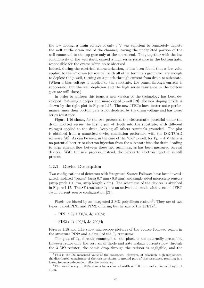
Figures 1.22 shows gate current versus drain voltage. Note how the gate currentincreases rapidly for drain voltages in excess of 3 V. This at first would appearto be due to avalanche multiplication in the reverse biased gate-drain junction;however, the fact that the current is lower at VGS = −1 V than at VGS = 0 –despite the higher value of VGD – shows that a different interpretation is needed.Further insight can be obtained from the “complementary” Figure 1.23, showingIG versus VG, for different values of VDS : when the gate voltage becomes morenegative, the gate-drain junction becomes more reverse biased, but the gate cur-rent decreases. Instead, the current increases at higher values of the drain-sourcevoltage (controlling the field in the pinched-off region of the channel) and at morepositive values of the gate voltage (increasing the channel current).This indicates that the multiplication process is due to impact ionization by theelectrons making up the channel current, in the high-field region near the drain [22].The generated electrons flow to the drain, adding up to the channel current; how-ever, their effect is hardly noticeable because the channel current is much largerthan this contribution from impact ionization. The generated holes are collectedon the gate, leading to a dramatic increase of the otherwise very small gate current(as shown by Figure 1.23). In any case, our operating voltage is VDS ≃2.5 V, in a
30

-2.0 -1.5 -1.0 -0.5 0.01p
10p
100p
1n
10n
100n
1µ
10µ
100µ
1m
10m
g m (S
) or
I dr
ain
(A)
V GS (V)
gm I drain
Figure 1.21: Input characteristic ID-VGS of the 1000/4 JFET test structure. ID
and gm are plotted for VDS = 2 V.
200/4 400/4 500/4 1000/4
gm @ VGS = 0V 3.0 5.8 6.9 14.3gm @ VGS = −0.2V 2.5 4.7 5.6 11.6gm @ VGS = −0.4V 1.9 3.5 4.2 8.8gm @ VGS = −0.6V 1.2 2.2 2.9 5.8
Table 1.3: Trasconductance gm (in mS) of every measured test structure.VDS =3 V.
region where the multiplication effects can be neglected even for the gate current.
Table 1.3 shows the gm values measured on the test JFETs. It can be seenthat they scale reasonably well with the channel width W . The scaling is less goodfor the 500/4 device, because it is made of 4 times shorter “fingers”, leading to alarger influence of the “border effects”.
In the source follower configuration, the current flowing into the channel of theJFET JS is fixed by the saturation current of JC, acting as a current source. Thiscurrent defines the gate-source voltage of JS .Both JFETs are expected work in saturation; in order to reach this condition,the supply voltages VDD and VSS (Figure 1.17) must exceed some minimum val-ues. Table 1.4 lists the operating point of the JFETs, as adopted for the noisemeasurements.
31
0 1 2 3 4 5 6100f
1p
10p
100p
1n
10n
100n
I gat
e (A
)
V DS (V)
V GS = 0 V V GS = -0.8 V V GS = -1 V
Figure 1.22: Gate current of the 1000/4 JFET versus VDS , for different values ofVGS. IG shows avalanche multiplication for VDS & 3 V.
-2.0 -1.5 -1.0 -0.5 0.0100f
1p
10p
100p
1n
10n
100n
1µ
I gat
e (A
)
V GS (V)
V DS = 6 V V DS = 5 V V DS = 4 V V DS = 1 V
Figure 1.23: Gate current of the 1000/4 JFET versus VGS, for different values ofVDS.
32

PIN1 PIN2 STRIP
Idrain (mA) 4.34 1.41 0.285Vgate of JS (V) 0 0 1.5 (2)VSS (V) -3 -3 0VDD (V) 3 3 3 (4)VGS of JS (V) -0.45 -0.34 0.77VDS of JC (V) 3.45 3.34 2.27 (2.77)VDS of JS (V) 2.55 2.66 0.73 (1.23)gm (mS) 10.7 4.62 1.7
Table 1.4: Operating points of the JFETs of the devices bonded and used asdetectors.
200/4 400/4 500/4 1000/4
CGD @ VSG = 0 V 1.44 1.57 2.34 4.36CGD @ VSG = 0.2 V 1.55 2.34 4.28CGD @ VSG = 0.4 V 1.53 2.31 4.17CGD @ VSG = 0.6 V 1.52 2.29 4.09CGD @ VSG = 0.8 V 2.28 4.05
Table 1.5: Gate-drain capacitance for Vdrain = 3V . Gate to LOW. Source to SMU.2.7µF connected from source to ground. Values in pF.
1.2.3 AC measurements
For noise measurements, the capacitance entering noise expressions is the one seenby the gate of the input transistor. In the source-follower configuration, the gate-source capacitance does not contribute: since VGS is kept constant by the followereffect, this capacitance does not charge up. We then need to know only the gate-drain capacitance. The JFETs have been designed to have one more finger in thesource than in the drain, so that the gate-drain capacitance is smaller.
We have measured the capacitance CGD versus VDG for several values of VGS .The results for VGD = 3 V are shown in Table 1.5. Because the gate is kept at0 V by the LOW terminal of the LCR meter (see Appendix A), while the drainis connected to the HIGH terminal (supplying the vAC signal and the VDG bias),we must provide an additional DC voltage to the source and, at the same time,we must keep it at ground for what concerns the AC signal. The SMU we use asvoltage source is not expected to give a good AC ground, so we connected a largevalue capacitor C0 between source and ground (except in the measurements withthe source at 0 V, when the source has been directly connected to ground). Thiscapacitor in some conditions causes the SMU to oscillate (this is why Table 1.5has white boxes).
The value of C0 must be chosen large enough to make its impedance smallcompared with that of the channel; the channel resistance 1/gd in Figure 1.20 hasa minimum value of 100 Ω at VGS = VDS = 0. At the measurement frequencyof 100 kHz, (ωC)−1 = 100Ω when C = 16 nF, so that with the used capacitanceC0 = 2.7µF the source is kept efficiently at ground.
The gate capacitance has been measured to be frequency independent in a
33
0 1 2 3 4 5 60
2p
4p
6p
8p
10p
C
GD
(F)
V drain (V)
V GS = 0 V V GS = -0.8 V
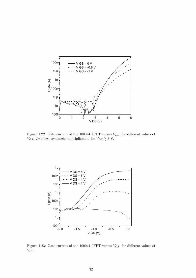
Figure 1.24: Gate-drain capacitance versus VDG for a 1000/4 JFET, with VGS = 0and -0.8 V.
wide range of frequencies, as expected for a reverse biased junction as long asseries resistance is not an issue. A relatively high frequency of 100 kHz has beenchosen, to make the admittance of the 2.7 µF capacitance much larger than theconductance of the channel and to increase the accuracy of the measurement.Looking at Figure 1.24, we note that the capacitance increases more rapidly at lowdrain voltages, when the JFET is in its “linear” region: in this case the channel isin ohmic contact with the drain, so that a fraction of the gate-channel capacitance(the other end of the channel is kept at AC ground by the source) contributesto the gate-drain capacitance. In the saturation region the capacitance shows amodest dependence on VGD and VGS . The dissipation factor is low (below 1%) forVGD . 5 V.
From Table 1.5 we see the capacitance approximately scales with the channelwidth for the 1000/4 and 400/4 JFETs, that have similar geometry. The 200/4JFET has a different structure, with only one gate and one source finger, 200 µmlong, and the perimeter of the gate running all around the drain is the same asfor the 400/4 JFET: hence the very similar capacitance values. The 500/4 JFET,on the other hand, has a higher capacitance than expected from scaling; this canbe easily explained by considering border effects, which in this structure are moreimportant due to the shorter fingers, as noticed for the transconductance values.
34

Chapter 2
Models for Noise Analysis in
Silicon Detectors
Often the most important feature limiting the performances of a system is itsinherent level of noise. This is a measurable quantity and can be expressed inmany ways. The signal to noise ratio indicates, for a specific type of event, theratio between the signal (assumed to be noise-free) and the rms noise. Since mostdetectors rely on the measurement of the charge delivered by an ionization event 1,the most common parameter used to characterize the noise is the equivalent noisecharge (ENC), defined as the input charge that produces at the output a signalamplitude equal to the rms noise.It is the minimum charge detectable by the system, the one making the signalto noise ratio equal to 1. In any detector, minimizing the ENC could not be theonly issue. As an example, consider a detector working at high rate: if the signalsare processed too slowly, phenomena like pile-up may occur; consider also cases inwhich the charge needs time to be collected at the electrode: a longer signal helpscollecting the total charge avoiding the so called ballistic deficit. Anyway, even itis meaningless to talk about the best detector, a best detector can be found forevery application. Now, we present the theory underlining the philosophy of pulseprocessing. This argument has been discussed many times and long ago, it is a fullunderstood issue and largely used: we do not have the purpose of presenting thedetails of the theory, we just present the underlying ideas. Since in this work wewill use two type of preamplifiers (charge and voltage sensitive ones) we describejust these two, skipping the current sensitive one. First, a brief review of the noisesources we are dealing with is presented.
2.1 Noise Sources in Detector Systems
In any physical system, measurable quantities come with some sort of unavoidablesuperimposed fluctuations, due to the discrete nature of matter or the quantityitself or to the randomness of the constituting processes [23]. All these fluctua-tions take the name of “noise”; it is a statistical property of the system and canbe estimated and measured. Obviously, it could be minimized, and often this is
1The charge produced by an ionization event is proportional to the energy deposited into thedetector material. In Silicon, an average energy of 3.6 eV is required to create an electron/holepair
35

the most important aim of the system designer.Consider a process, no matter the quantity involved, represented by the real func-tion of time x(t). It spans from −∞ to +∞ and of such a process we want tocalculate the Fourier transform. This may seem hopeless, because one conditionfor the existence of the transform function X(ω) is that x(t) must be absolutelyintegrable, i.e.:
∫
∞
−∞
dt|x(t)| < ∞ (2.1)
but this condition does not hold, since x(t) does not decay to zero at ±∞. |x(t)|2 isrelated to the energy carried by the physical process and it is clear that the energyincreases with time. However, our measurement times are never infinite and we areinterested in statistical quantities independent of the time of observation. CallingT the observation time, we can define a new function from x(t), coincident withx(t) inside the window ±T
2 and null outside:
xT (t) =
x(t) if − T2 < t < T
20 outside
(2.2)
The gated (or truncated) function xT (t) is now absolutely integrable, so that itsFourier Transform exists
XT (ω) =
∫
∞
−∞
dt xT (t)e−iωt (2.3)
and, by Parseval’s theorem (or energy theorem):∫
∞
−∞
dt|xT (t)|2 =1
2π
∫
∞
−∞
dω|XT (ω)|2 =1
2π
∫
∞
0dω 2|XT (ω)|2 (2.4)
Since xT (t) is a real process, the module of its Fourier Transform |XT (ω)| is aneven function, allowing the integral
∫
∞
−∞dω to become, as written,
∫
∞
0 2 dω. Both
sides of the equation above represent the energy of the process 2 and are finiteas long T < ∞. The quantity 2|XT (ω)|2 can then be interpreted as the energyspectral density of the process, which has units of energy/Hz.
Dividing both sides by the observation time T we get the average power in thegated process xT (t):
1
T
∫ T2
−T2
dt|x(t)|2 =1
T
∫
∞
−∞
dt|xT (t)|2 =1
2π
∫
∞
0dω
2|XT (ω)|2T
(2.5)
For the stationary noise processes we are interested in, it is reasonable to assumethe existence of the limit:
limT→∞
1
T
∫ T2
−T2
dt|x(t)|2 (2.6)
which can then be taken to represent the average power of the ungated processx(t). Then:
limT→∞
1
T
∫ T2
−T2
dt|x(t)|2 = limT→∞
1
2π
∫
∞
0dω
2|XT (ω)|2T
= (2.7)
2They are actually proportional to the energy, with a dimensioned proportionality constantthat depends on the nature of the process considered. For brevity, this proportionality constantis usually understood, and the expression above is conventionally called the energy of the process.
36

1
2π
∫
∞
0dω[ lim
T→∞
2|XT (ω)|2T
]
where we have assumed that the limit T → ∞ and the integration over ω canbe interchanged. It is then natural to define the power spectral density of theprocess x(t) as:
dx2
df= lim
T→∞
2|XT (ω)|2T
(2.8)
The power spectral density just defined is referred to as the “unilateral” spec-tral density; often, as in [11], the “bilateral” power spectral density is used, wherethe factor 2 in the numerator of 2.8 is absent and the integral extends from −∞to +∞.
If x(t) is the input of a linear network3, it is straightforward to determine thepower spectral density at the output of the system due to the input x(t). If h(t)is the response of the system to a δ-like impulse, then the output correspondingto the input waveform x(t) is given by the convolution product:
xout(t) =
∫ +∞
−∞
dt′ x(t − t′)h(t′) (2.9)
In the frequency domain, this translates into the simple product of the FourierTransforms:
Xout(ω) = X(ω)H(ω) (2.10)
Noise spectral densities are proportional to the square of the modulus of the Fouriertransforms. Then, taking the square of the modulus of the expression above, weget:
dx2out
df=
dx2
df|H(ω)|2 (2.11)
Integration over all frequencies gives the rms value of the output quantity xout(t).These concepts are already sufficient to derive the contributions of some of themost relevant noise sources.
2.1.1 Shot Noise
We illustrate the characteristics of shot noise by considering the current associatedwith random emission of carriers over a potential barrier. Example of this kindof process are the thermionic emission of electrons from a cathode in vacuumtubes, or the emission of holes or electrons by the punch-through mechanism insemiconductor devices. Considering a time T , in which N emissions are observed,the current can be expressed in the time domain as:
i(t) = qN
∑
k=1
f(t − tk) (2.12)
where q is the electron charge, and f(t − tk) gives the time dependence of thecurrent pulse produced by a carrier emitted at time tk. Since the integral of this
3a linear network is one for which the superposition law applies: in our case the preamplifier-shaper chain can be approximated as linear, i.e. we assume the signal amplitudes are small enoughfor the small signal analysis to apply
37

pulse must be equal to q, we have:∫ +∞
−∞dt f(t) = 1. The Fourier transform of
such a process is:
I(ω) = qF (ω)
N∑
k=1
eiωtk (2.13)
with the corresponding power spectrum:
limT→∞
q2 2|F (ω)|2T
N∑
k=1
N∑
m=1
eiω(tk−tm) (2.14)
The summation can be decomposed into one considering the terms k = m andanother considering the terms k 6= m. The first gives just the number N of pulsesin the interval T , the other accounts for the DC level of the current [23]. Neglectingthe second term, we obtain the power spectral density:
di2
df= lim
T→∞
q22|F (ω)|2 K
T= 2q2ν|F (ω)|2 = 2qI|F (ω)|2 (2.15)
where limT→∞ q NT = qν is the DC current. Notice that, in the case the pulses are
extremely sharp, to be considered as delta pulses, the power spectrum assumes thewell known expression:
di2
df= 2qI (2.16)
Since all frequency dependent terms are inside |F (ω)|2, the noise is white, i.e.frequency independent, at least in the range of frequencies for which the physicalpulse can be considered as δ-like: ω << ∆t−1, where ∆t in the “duration” of thecurrent pulse.The leakage current thermally generated via SHR traps in a semiconductor devicehas the same spectral power density 2qI [23], because it results from the superpo-sition of current pulses generated by randomly emitted carriers.
2.1.2 Thermal Noise
A resistor in thermal equilibrium with its surroundings shows a noise voltage atits terminals, i.e. the open circuit voltage has a value different from zero, due tothe thermal motion of the electric charges in a conductor. This phenomenon wasdiscovered by Johnson back in 1928 [24], and in the same year the expression forthis noise was first derived by Nyquist [25], on the basis of the second law of thethermodynamics, considering the power exchanges between a couple of resistors inthermal equilibrium.Nowadays, this noise is referred to as “Johnson” or “thermal” noise.He found that the noise voltage power spectral density is flat (“white”) and hasthe value:
dv2
df= 4kTR (2.17)
Any physical resistor shows this kind of noise.In the analysis of electronics devices, one often encounters “effective” resistances,not related to an ohmic conduction process and calculated from the slope of thecurrent-voltage characteristic of the device. It is important to notice that nothermal noise is associated with these resistances [26].
38

4kT gΓ m
GSC
GDC
4kT gΓ m
RS gmvG’S+4kTR
fA
s
+4kTRfA
s
gate2qI
gate2qI
G
S
DG’
G
S
D
Figure 2.1: Location of the noise sources in a JFET. Also depicted is its relevantsmall signal model.
2.1.3 1f
noise
While shot noise and Johnson noise are white noises, i.e. frequency independent, atleast in the frequency range of interest in most physical cases, there are very com-mon noise sources showing strong frequency dependence. The so called “flicker”
noise comes with a power spectral density ofA1/f
f and it is present in almost everyelectronic device. Trapping and detrapping processes, in which a carrier is trappedand released with a given time constant, generate a pure Lorentzian noise, havinga power spectral density ∝ f−2. Very seldom a single time constant is involved,and with just a few values of time constants spread across a couple of decades,Lorentzian noise sums up to an almost perfect f−1 spectrum [26]. Usually, werefer to this kind of mechanism to explain flicker noise, related to some kind ofimperfections of the material. It is clear that, in devices more affected by imper-fections, the 1/f noise will be greater [27]. MOSFETs are particularly afflicted,being surface effect devices; JFETs are less sensitive, relying for their functioningon bulk effects.
2.1.4 Noise in JFETs
The noise sources in junction field-effect transistors are: leakage current of thegate, gate spreading resistance, thermal noise in the channel, flicker noise in thechannel.The gate leakage current is usually negligibly small in the JFETs used for spectro-scopic applications. This current comes from carrier generation in a reverse biasedjunction. Its noise current spectral density is: di2
df = 2qIleakage.Gate spreading resistance accounts for series resistance of the gate. Usually thisnoise contribution is small; its voltage spectral density is dv2
df = 4kTRgate.The resistance of the channel can be expressed in terms of the transconductancegm as (Γgm)−1, where the corrective factor Γ has a value of about 2/3 [8]. This
gives at the drain a noise current with spectral density di2
df = 4kTΓgm. Channelnoise can be referred back to the gate via the transcondunctance, leading to avoltage spectral density dv2
df = 4kTΓgm
. Summarizing, all noise sources in the JFETcould be thought of as applied at the gate and described by an input noise voltage(Figure 2.1) .
39

Rf
Cf
outv
Rf
Cf
outvDCinC inC
Rbias
CA
DCdi2df
dv2
df
Figure 2.2: Fundamental elements of a Charge Sensitive Amplifier (CSA), thedetector (represented by its capacitance) is DC-coupled (left) and AC-coupled(right) to the CSA. Also shown, the noise sources.
2.2 Charge Sensitive Amplifier Configuration
The CSA (Figure 2.2) can be seen as an operational amplifier (OPA) whose out-put is connected by a feedback capacitance to the inverting input, while the non-inverting input stays at some fixed potential, equivalent to ground for the small-signal analysis. The detector is connected to the inverting input. When a chargeQ0 is delivered by an ionization event, this charge does not accumulate on the de-tector capacitance, because the voltage across it is kept constant by the feedbackloop, but flows to charge up the feedback capacitance Cf , giving at the outputa step signal, whose amplitude is −Q0/Cf . Since the input transistor is usuallya JFET, providing very high input impedance, the feedback capacitance is thelowest impedance path to the signal.The detector can be DC or AC coupled to the CSA. In the first case, the biasresistor, with its associated thermal noise, is absent, so that the overall noise per-formance is expected to be better. The leakage current flows directly throughthe feedback path, charging up the capacitance, exactly as the signal charge does.Thus the output voltage will increase with time, eventually reaching saturation.It is then necessary to provide a DC path for the current: the simplest way isplacing a feedback resistor in parallel with the feedback capacitor. This resistortoo contributes a noise current at the input of the CSA, but it can be easily madeof larger value than the bias resistor when the latter needs to be integrated on thedetector. The signal charge, initially stored on the feedback capacitor, is also dis-charged through the feedback resistor, causing the output to decay exponentiallywith time constant given by the product RfCf . An alternative solution, adoptedin many practical cases, is the introduction in the feedback path of a reset transis-tor. The leakage current initially is integrated onto the feedback capacitance; toprevent saturation, at suitable times the reset transistor turns on and dischargesthe feedback capacitance through a low resistance path. This has the advantageof not introducing additional noise sources, if we can neglect the very low leakagecurrent of the transistor in its OFF state. Furthermore, in integrated circuits,where space is a concern, a transistor is many times smaller than a resistor. Thislast kind of CSA is called a reset-type one.In this work, only amplifiers with continuous draining of charge trough a feedbackresistor will be considered. In detectors with many electrodes, such as strip or pix-
40

els, it is preferable to AC couple the sensor to the preamplifier, by interposing alarge value capacitor between them. This will prevent high leakage currents origi-nating in defective strips or pixels from affecting the working point of the front-endelectronics. A bias resistor will also be required, in order to apply bias to the de-tector and provide a path for the leakage current. The coupling capacitance mustbe large enough to, on one hand, favourably compete with the detector and straycapacitances, and on the other hand, have an impedance, in the frequency rangepassed by the filter following the CSA stage, much lower than the bias resistor.Even with AC coupling, a feedback resistor in the CSA (or a reset transistor) willstill be needed, in order to stabilize the input against stray charges and currents.However, this resistor can be taken of larger value than the bias resistor, so thatits contribution to the noise will not be important. Consider now, the effect of thenoise sources on the output of the CSA. Noise current sources at the input, indi-cated with the symbol di2
df , charge up the feedback capacitance, giving an outputnoise voltage:
dv2out,i
df=
1
ω2C2f
di2
df(2.18)
Notice how the white spectral density of the current noise becomes strongly depen-dent on frequency. Noise voltage sources at the input (dv2
df ) produce at the outputa noise voltage which can be determined by considering the voltage divider givenby the feedback and input capacitances. That voltage is then:
dv2out,v
df=
dv2
df
(Cin + CD + Cf )2
C2f
(2.19)
where CD is the capacitance of the detector, and Cin accounts for the input ca-pacitance of the first JFET of the front-end electronics, as well as for the parasiticcapacitance in the connection between detector and electronics.These noise voltages, carrying informations on some of the relevant detector andfront-end electronics features, come out from the CSA, which has low outputimpedance, and feed the following stage, the shaping amplifier. The latter per-forms a filtering in the frequency domain, with the purpose of enhancing the signalwith respect to the noise. The shapers considered in our studies are time-invariantones: that is their action does not depend explicitly on time.If a step function enters the shaping circuit, it gives at the output a pulse of adefined “shape”. In the frequency domain, if this shape has the Laplace TransformF (s), then we have [11]:
F (s) =1
sT (s) (2.20)
where 1s is the Laplace Transform of the input step and T (s) is the transfer function
of the shaper, defined as the Laplace transform of the output pulse correspondingto a δ-pulse at the input 4. With this definition, we can express the noise voltage
4In our definition, differing from the one reported in [11], the amplitude of output shapef(t) = L
−1(F (s)) is normalized to unity. This has the advantage that the signal acquired by theamplification chain:
S =Q0
CfA MAX(L −1(F (s))) (2.21)
with A the gain of the amplification stage, simplifies in: S = Q0
CfA
41

r.m.s. at the output of the shaping amplifier as:
σ2v =
∫
∞
0dω
dv2out
df|T (iω)|2 = (2.22)
∫
∞
0dω (
di2
df
1
ω2C2f
+dv2
df
(Cf + Cin + CD)2
C2f
)|T (iω)|2
where the contributions of both input noise current and input noise voltage havebeen considered. The signal to noise ratio is then:
S
N=
Q0/Cf√
σ2v
=Q0
√
∫
∞
0 dω (di2
df1
ω2 + dv2
df (Cf + Cin + CD)2)|T (iω)|2(2.23)
Notice that the Cf factors cancel each other. The ENC is the signal charge thatmakes S
N = 1. Expressed in coulomb, it is just the denominator; dividing it by theelementary charge q we get the more usual expression in terms of electrons. Then,summarizing, the contributions to the ENC of the various noise sources are foundto be:
- current or parallel noise:
ENC2parallel =
∫
∞
0dω
di2
df
|T (iω)|2ω2
(2.24)
- voltage or series noise, both white and flicker:
ENC2series =
∫
∞
0dω
dv2
df(Cf + Cin + CD)2|T (iω)|2 (2.25)
The above reported integration is often impracticable to perform analytically;with numerical techniques, however, it is easy to obtain an accurate result. Expres-sions derived for many types of shaping functions are available in literature [11].Derivation of noise level can be carried on also in the time domain [28]. With thisapproach, the transfer function of the circuitry following the CSA is not used andthe filtering action is replaced by the shaping one, then a frequency function is re-placed by a time function. The calculation in the time domain begins consideringthe causality of noise process: during the processing of the signal, care should betaken of all noise events which occurred at previous times, whose effects last untilmeasurement time.Campbell theorem states that, at any time, the variance of a process is given bythe sum of the squares of all preceding contributions at that time.In our case, in particular, noise current is given by independently emitted charges,each one giving a step pulse at the output of the CSA which is then processedby the filtering stage: the “shaper”. If a charge q is emitted at time t0 and theshape transforms the step of magnitude q
Cfat the output of CSA into a shape
qCf
f(t − t0), it gives a contribution to the measured signal at the measurement
time tm of:
v(tm) =q
Cff(tm − t0) (2.26)
42

To calculate the variance of of the process, we must take into account all the noiseevents occurring at times t0i < tm and sum up their square contributions at thetime tm. The variance of the process is then [28]:
σ2v,i =
q2
C2f
Σif2(tm − t0i) (2.27)
and the symbol σ2v,i stands for the variance of the output voltage, produced by
noise current. Passing at the integration level, possible since the rate of arrival ofthe pulses is far greater than the times involved in any physical calculation:
σ2v,i =
q2
C2f
< n >
∫
∞
0dtf2(t) (2.28)
Notice that the term q2 < n >= qI is one half of the shot noise. We can readilyextend the concept and say that, limited for the current noise, whose pulses inte-grate onto the feedback capacitor, the noise at the output of the shaper is givenby:
σ2v,i =
1
C2f
1
2
di2
df
∫
∞
0dtf2(t) (2.29)
If noise current, originated from δ pulses, produces steps at the output of the CSA,noise voltage, originated by δs too, transmits as it is at the output of the CSA; sothere is an operation of derivation between them. If a δ gives a f(t), a derivativeof a δ, let’s call it the doublet δ′, gives the function δ′ ⊗ f(t) = f ′(t). The noisecontribution given by the voltage white noise is:
σ2v,v =
(Cin + Cf + CD)2
C2f
1
2
dv2
df
∫
∞
0dtf ′2(t) (2.30)
and the symbol σ2v,v stands for the variance of the output voltage, produced by
voltage noise. Normalizing the shape at some fixed peculiar time, maybe thepeaking time or some shaping time defining the curve, we can have an expressionmaking explicit such times:
I1 =1
2
∫
∞
0dt f2(t) = τa1 (2.31)
I2 =1
2
∫
∞
0dt f ′2(t) =
a2
τ(2.32)
if, of course, just one time is involved. Any shaper has its own numerical coefficientsa1, a2; they have been tabulated for a large number of pulse response.Unfortunately, calculation of ENC following the easier time domain is not trivialfor a “coloured” noise spectral density, only white noise can be treated with thiscalculations. Then, in calculation of the 1/f noise contribution we must rely onfrequency domain methods5. The 1
f noise comes from a voltage noise, as seen inFigure 2.1, and expressing it with the aid of the constant A1/f :
dv21/f
df=
A1/f
f(2.33)
5On the other hand, dealing with time variant shapers, only time domain approach is feasible.
43

To have the 1f contribution to the total output noise v2, just calculate the integral:
σ2v,1/f =
∫
∞
0dω|T (iω)|2
A1/f
f
(Cf + Cin + CD)2
C2f
=(Cf + Cin + CD)2
C2f
Af (2.34)
independent of the peaking time. It is a feature of the exact 1f power noise spectral
density, and does not depend on the filter involved. This comes out because thefiltering action selects a passing band, whose lower and upper limit scale with thesame factor, changing the peaking time of the shaper. Indeed, since
∫ fup
fdowndf 1
f ∼log
fup
fdown, there are no frequency or time dependencies in the final results.
The total noise voltage can be expressed as:
σ2v = σ2
v,i + σ2v,v + σ2
v, 1f
= (2.35)
di2
df
1
C2f
τa1 +dv2
df
(Cin + Cf + CD)2
C2f
a2
τ+
(Cf + Cin + CD)2
C2f
Af
Since the input signal is ∝ C−1f , the ENC (expressed in number of electrons) takes
the well known expression [28]:
ENC2 =di2
dfτa1 +
dv2
df(Cf + Cin + CD)2
a2
τ+ (Cf + Cin + CD)2Af (2.36)
showing the three components, each having a different dependence on the peakingtime τ , as shown in the example of Figure 2.3.
2.3 Source Follower Configuration
The configuration adopted for the readout employing a source-follower (SF) asfirst stage of signal processing is illustrated in Figure 2.4. The JFET JC actsas a current source, setting the working point of JS . The output of the SF isAC coupled by the capacitor CA to an external charge-sensitive amplifier. Thesignal generator can be represented as a current source delivering a short pulse ofcurrent, typically shorter than a few tens of nanoseconds; in many cases this maybe approximated by a δ-like pulse of current. The signal charge is integrated on thecapacitance at the input of the SF rather than on the feedback capacitance of theCSA, and is then discharged through the RC equivalent circuit of the input node.R is the bias resistance, through which the leakage current flows. C = CD + CGD
is the total capacitance seen by input, with the important exclusion of the FETgate-source capacitance, which does not contribute because it is bootstrapped bysource follower action (its two terminals have the same voltage). The small signalvoltage at the gate of the JFET is then [29]:
vin(t) =Q0
CD + CGDe−
tR(CD+CGD) =
Q0
Ce−
tRC (2.37)
with the Laplace Transform:
vin(s) = Q0R
1 + sR(CD + CGD)(2.38)
44

0.1 1 10
200
300
400
500
600700800900
1000
EN
C
peaking time ( s)
total parallel 1/f series
Figure 2.3: ENC (Equivalent Noise Charge in electrons r.m.s.) for a CSA followedby a triangular shaper, as a function of the shaper’s peaking time. The parametersare: a1 = 1
3 , a2 = 1, Cf +Cin +CD = 10 pF, di2
df = 2qIleakage with Ileakage = 1 nA,dv2
df = 4kTΓgm
with gm = 13 mS and Af = 10−12 V 2.
The output voltage of the SF driving the capacitive load CA can be expressed inthe s domain as:
vin(s)
1 + gS+gC+sCAgm,S
(2.39)
Since the output conductances gS , gC of the two transistors are much smaller thanthe transconductance gm,S of JS and in addition sCA << gm,S (as will be discussedlater), the output voltage of the SF closely follows the input. In the following, wewill then assume that the output of the SF equals the input. The following stageof amplification is again a OPA in CSA configuration, but now the combinationSF + CSA behaves as a voltage amplifier, giving at the output:
vout(s) = −vin(s)CA
Cf
sRfCf
1 + sRfCf= −Q0R
CA
Cf
sRfCf
(1 + sRC)(1 + sRfCf )(2.40)
Transforming this back to the time domain:
vout(t) = −Q0
C
CA
Cf
RfCfe−t
RC − RCe−
tRf Cf
RfCf − RC(2.41)
The output is the difference of two exponential falls, one with time constant RCand another with time constant RfCf . As mentioned in section above, it is difficultto integrate a very large value resistor on the detector, since this would increase toan intolerable extent the dead area, so it often comes out that RC = R(CD +CGD)is much smaller than the feedback time constant RfCf . The signal may then be
45

Rf
fCSJ
CJ
outv
inv~
inv
dvSF2
dfbiasR
CD
di2pdf AC
dv2
df
inC
di2df
CSA
Figure 2.4: Schematics of a detector read-out by a Source Follower. Also shown,the noise sources.
approximated by a single exponential decay, with time constant set by the detectorRC. If the shaping time is not much shorter than this time constant, a decrease inthe pulse height occurs, with a consequent reduction in S/N.
With respect to the CSA configuration, the signal at the shaper’s input ismagnified by the factor CA
C = CACD+CGD
, that could be made large choosing largevalues for the coupling capacitances CA. The limit to the value of CA comes fromtwo considerations: first, the JFET JS takes a time CA/gm to charge up CA or,expressed in the frequency domain, the output impedance of the JFET (g−1
m ) mustbe by far smaller than 1/ωCA; second, the value of the capacitor is limited by spaceconstraints when it needs to be integrated on the silicon wafer. With respect tothe CSA configuration, the signal at the shaper’s input is, indeed, CA
CD+CGDtimes
greater. The signal acquired is, considering unity gain of the shaper response:
SSF =Q0
CD + CGD
CA
Cf(2.42)
Let’s calculate the expecteddv2
outdf at the output of CSA, knowing the noise sources
and the transfer function of the system. Just enumerate the noise sources [30]:
-di2pdf = 2qIL + 2qIgate + 4kT
R is the noise current at the input of the JFETJS . It is made up by the leakage current of the detector, the leakage of thegate of the input JFET and the Johnson noise of the biasing resistor. As thesignal does, it passes through the RC of the detector, giving by generalizedOhm law a small signal voltage at the gate of the FET. Then, at the outputof the CSA:
dv2out,ip
df=
di2pdf
(CA
Cf)2
R2
1 + (ωR(CD + CGD))2(2.43)
Two case are worth distinguishing: at short shaping times compared withRC, that is at high frequency, the denominator of the expression above isproportional to ω2, behaving as parallel noise:
dv2out,ip
df=
di2pdf
(CA
Cf)2
1
ω2(CD + CGD)2(2.44)
46

RBias 1M gm,S 5 mS
CD 5 pF gm,C 1 mS
CGD 2 pF gm 10 mS
Cin 15 pF Af,S 0
CA 15 pF Af 10−12V 2
Table 2.1: Unless differently specified, parameters entering noise expressions forthe SF read-out, used to calculate the plots 2.5 through 2.8.
on the other hand, at long shaping times, or low frequencies, the ω2 depen-dence disappears, as in the case of series noise:
dv2out,ip
df=
di2pdf
(CA
Cf)2R2 (2.45)
Notice how also this noise is amplified by the ratio CACf
, exactly as the signal
is.
-dv2
SFdf = 4kTRGate,S + 4kT Γ
gm,S+
A 1f
,S
f + 4kTΓgm,C
g2m,S
is the series noise of the
input devices (the two JFET of the source follower), comprehensive of the1/f noise of the JS , that is reproduced identical to the drain of JC and givesa contribution:
dv2out,SF
df=
dv2SF
df(CA
Cf)2 (2.46)
- dv2
df = 4kTRGate + 4kT Γgm
+A1/f
f is the series noise of the CSA amplifier,essentially the noise of input FET, referred to the gate of its input FET. Itgives a contribution to the output:
dv2out,v
df=
dv2
df(CA + Cin + Cf
Cf)2 (2.47)
where Cin is the input capacitance of the input FET plus parasitic capaci-tance in the connections from CA to CSA. Note that for applying the formulaof the voltage divider the impedance must be at ground and CA does notseem to be at; instead, since the input impedance of JS is low, practicallywe can consider CA at ground.
- di2
df = 4kTRf
is the parallel noise at the input of the CSA amplifier, essentially
the noise of the feedback resistor. It contributes as:
dv2out,i
df=
di2
df
1
(ωCf )2(2.48)
-dv2
shaper
df : not always we can neglect the noise introduced by the shaper, wewill see later a case when this really happens. Obviously, being at the output,it contributes as it is at the output.
47

0.01 0.1 1 10 100 100010
100
1000
EN
C
peaking time ( s)
total 1M series-parallel 1M series-parallel 10M total 10 M 1/f series
Figure 2.5: Model for the noise expected in a detector read-out by a SF; theparameters used are those listed in table 2.1. Series, 1/f and bias resistor noisecontributions are shown, as well as their sum. Bias resistors of 1 MΩ and 10 MΩare considered.
Next step, let’s pass these noise spectral densities through the shaper:
σ2v =
∫
∞
0dω|T (iω)|2 dv2
out
df(2.49)
Many of these contributions may be calculated in the time domain, since they areoriginated from white noise and have expressions similar to the ones described inthe CSA case. The most interesting part is the one with the peculiar denominator1+ω2(R(CD +CGD))2, behaving as voltage or current noise depending on whetherthe shaping time is greater or smaller than the input time constant.We can take advantage of the integral expression calculated for the CSA case, tofind out the ENC contribution of each noise source, shown in Figure 2.5.
-di2pdf is the noise coming from the “parallel” sources before the first amplifica-tion stage, the SF itself. The major contribution is easily given by the biasresistor. Let’s consider the two limiting cases: at high frequency, this noiseis a parallel one and:
ENC2ip,ω→∞
= (2qIL + 2qIgate +4kT
R)a1τ (2.50)
while at low frequency:
ENC2ip,ω→0 = (2qIL + 2qIgate +
4kT
R)(CD + CGD)2R2 a2
τ(2.51)
Considering that usually we try to keep the shaping times small, in order toincrease the acquisition rate, this noise is essentially parallel and the expres-sion ENC2
ip,ω→∞holds. It turns out that the expression is identical to the
48

0.01 0.1 1 10 100 1000
200
400
600
800
1000
EN
C
peaking time ( s)
CA = 7 pF CA = 15 pF CA = 1 nF
Figure 2.6: Effect of the coupling capacitance CA on ENC: plots for CA = 7 pF,15 pF and 1 nF (practically infinite).
one for the CSA: the noise and the signal are indeed amplified by the sameamount and the capacitances, different in the two cases, play no role.
49

In general, the complete expression is6:
ENC2ip =
R2
τ
di2
df(1 +
a
2(−3 − e−
2a + 4e−
1a )) (2.60)
with a = R(CD+CGD)τ .
-dv2
SFdf is the voltage noise coming from the two JFETs making the SF. Sepa-
rating the white contribution from the 1/f one:
ENC2vSF ,white = (2.61)
(4kTRGate,S + 4kTΓ
gm,S+ 4kTΓ
gm,C
g2m,S
)(CD + CGD)2a2
τ
ENC2vSF ,1/f = Af,S(CD + CGD)2 (2.62)
These contributions are not present in the CSA case.
- dv2
df is the voltage noise coming from the external amplifier, configured as aCSA one but behaving as a voltage amplifier; again, separating the whitefrom the 1/f noise
ENC2v,white = (2.63)
(4kTRGate + 4kTΓ
gm)(
CA + Cin + Cf
CA)2
(CD + CGD)2a2
τ
6Unfortunately, to come to an exact and analytical solution, we must calculate by hand theintegral:
ENC2ip
=di2
df
Z
∞
0
dω|T (ω)|2R2
1 + (ωR(CD + CGD))2(2.52)
Considering a triangular shaper, |T (ω)|2 = 2π(ωτ)2
(1− cos(ωτ ))2 and setting a = R(CD+CGD)τ
and
x = ωτ , the integral “simplifies” to the new one:
ENC2ip
=di2
df
2R2
πτ
Z
∞
0
dx(1 − cos x)2
x2(1 + (xa)2)(2.53)
The integral, let’s call it “I”, can be proficiently decomposed to:
I =
Z
∞
0
dx(1− cos x)2
x2− a
2
Z
∞
0
dx(1 − cos x)2
1 + (ax)2(2.54)
Solving with some mathematical methods or with the aid of an integral table, the integrals give:
Z
∞
0
dx(1− cos x)2
x2=
π
2(2.55)
Z
∞
0
dx1
1 + (ax)2=
π
2a(2.56)
Z
∞
0
dxcos x
1 + (ax)2=
π
2ae−
1
a (2.57)
Z
∞
0
dxcos2 x
1 + (ax)2=
π
4a(1 + e
−2
a ) (2.58)
summing up to:
I =π
2+
aπ
4(−3 − e
−2
a + 4e−
1
a ) (2.59)
50

The contribution comes to its limiting value of
(4kTRGate + 4kTΓ
gm)(CD + CGD)2a2
τ(2.64)
increasing the coupling capacitance CA, being Eq. 2.63 a monotonically de-creasing function of this parameter, as can seen in Figure 2.6. Comparingwith the expression for the CSA:
ENC2v,CSA = (4kTRGate + 4kT
Γ
gm)(CD + Cin + Cf )2a2
τ(2.65)
we realize that deciding which one is greater depends strongly on the valueof the capacitance involved. Large Cin make the SF better, and then makingthat configuration preferable when parasitic capacitance, due to long wireconnection to the front-end amplifier, are not negligible. The same holdsconsidering the pink noise of the same second amplification stage:
ENC2v,1/f = Af (
CA + Cin + Cf
CA)2(CD + CGD)2 (2.66)
Deciding if it is better than CSA noise (CD + Cin)2A 1f
,1 depends again on
the capacitances.
- di2
df is the white noise coming from the Johnson noise of the feedback resistorRf :
ENC2i =
4kT
Rf
(CD + CGD)2
CAa1τ (2.67)
With CA larger than the input capacitance, this ENC can be made smallerthan the one in the CSA case.
At this point we must be able to compare the noise performances of the two typesof detector-amplifier chains with some numerical results.
2.4 Theoretical comparison of CSA and SF
As seen in the above sections, the parameters to be managed are a lot; so we are ledto make some approximation. Since this work is aimed to state the performancesof detector for high energy physics, only short peaking times are of interest, sothe noise
dipdf can be seen as parallel. The detector are supposed to have a very
large capacitance, deriving from gangling together several ones, and then the CGD
can be neglected. The same holds for Cf , that should be practically zero in everyapplication. For good devices, series resistances of the JFET gate are small; 1/fnoise can be neglected in first instance to simplify the overall calculations. gm,C
of the current source is less than gm,S , then also the noise coming from JC , can beneglected.
Consider, then, only the contributions coming from the thermal noise of thechannels of JFETs:
ENC2CSA = (CD + Cin)24kT
Γ
gm
a2
τ(2.68)
51

ENC2SF = C2
D4kTΓ((CA + Cin
CA)2
1
gm+
1
gm,S)a2
τ(2.69)
We are searching the condition for which the SF is better than the CSA:ENC2
CSA > ENC2SF ; this translates in a condition for the gm:
gm,S >gm
(1 + CinCD
)2 − (1 + CinCA
)2(2.70)
According to the expression above, when CA = CD then gm,S should be infinitefor the SF to be better than CSA, i.e. the JS must be noise free. In the very caseof CA < CD the expression shows that every gm,S ≥ 0 make the SF better, butthis is obviously due to a singularity of the function gm,S(CA) for CA = CD. Then,the condition is that CA > CD; it can be shown that even neglecting the thermalnoise in the channel of JS , the very white voltage noise of the CSA makes the SFconfiguration worst if CA > CD. This because the signal is under amplified by thefactor CA
CD< 1. In Figure 2.7, with all the parameters listed in table 2.1 and not just
considering the noise coming from some JFETs, the plots shows how the SF worksbetter than the CSA. The minimum gm,S , according to the formula, is gm
12 = 0.83mS. As expected, in the time range where series noise dominates, i.e. low shapingtimes, the SF configuration gives better noise performances than CSA. The regionin which the superiority of the SF holds less is the one where the parallel noise ofthe bias resistance begins to dominate: this contribution, indeed, does not dependon both capacitances or transconductances. At very high peaking times, howevertoo long to be practicable in whatever application, this bias resistance begins tocontribute as series noise, making SF better and better with respect to the CSA.
The introduction of integrated JFETs into the detector substrate is, of course,a complication of the process, requiring additional dopant implantations; but largeCin, sum of the input capacitance of the first FET and of parasitic capacitances,may justify it. It is worth plotting the expected noise in function of this parameterfor the two cases, at some fixed peaking time, possibly when series noise dominates- the other regions are not interesting. One typical result is plotted in Figure 2.8:for Cin smaller than 13 pF, the CSA is still better, then it worsens very rapidlywith respect to the SF. In this case, indeed, the Cin enters in the noise expressionsnever alone, but weighted with the CA, that must be made as high as possible, inthe ratio CA + Cin/CA.
2.5 Technological consideration
The supposed supremacy of the SF on CSA depends on many parameters and thesituation described above can be considered just as a first approximation. More,the SF needs some devices in the same silicon wafer of the detectors, compellingwith them for the available space and/or producing some power dissipation. Let’sconsider some limitations.
Rbias
Large Rbias must be chosen to decrease its Johnson noise. To make a large resistoris always an issue, since bias resistors are made with polysilicon whose resistivityper square ρs is of the order of 10 − 20 kΩ/. It is common, as in the previous
52

0.01 0.1 1 10 100 1000100
1000
10000
EN
C
peaking time ( s)
SF CSA
Figure 2.7: Comparison of the expected ENC for SF and CSA read-out versuspeaking time, with the two configurations sharing the same parameters as listedin table 2.1.
examples of silicon strip detectors, have bias resistors in a snaky configuration, toincrease their length. Anyway, the occupied surface is large and this fact puts ahigher limit to their value. However, considering low peaking times, parallel noisecoming from it may become low compared with the series sources of the channelthermal noises of the FETs; this can be the ultimate noise to cope with in SF.
CA
Large capacitances, as CA should be, require space. CA are integrated on the waferand are made of a thin layer of SiO2 between an external metal and a polysiliconlayer. The geometrical value, per unit area, is: ǫSiO2/tox, holding, for an oxidethickness of 200 nm 7, 0.17 fF/µm2. To have a “small” coupling capacitance ofjust 10 pF, the area needed is as large as 20k µm2; having a pitch, in a stripdetector, of 100 µm, in first approximation, considering complete area covering,we need capacitances 600 µm longer. It is not a negligible surface, and it comesin competition with the electrodes for charge collection.
JFET
It is possible to fabricate working JFET with the required characteristic of ca-pacitance and trasconductance, having a small pitch too. A possible geometry isthe interdigitated one, allowing high length/width ratios. In the plots above, weneglected the series contribution of the gate resistance, coming from the unmetal-lized regions of the gate implant, which could be even greater than the thermal
7the dielectric constant for the Silicon Oxide is 3.4 10−13 F/cm.
53

0 5p 10p 15p 20p 25p0
500
1000
1500
2000
E
NC
C in
SF CSA
Figure 2.8: Comparison of the expected ENC for SF and CSA read-outs versusthe input capacitance Cin, sum of the input capacitance of the CSA and of theparasitic capacitances. The peaking time is 100 ns, the other parameters are thoselisted in table 2.1.
noise of the channel.
54
Chapter 3
Experimental Set-up for Noise
Measurements
3.1 Detector Assembly
After testing the electrical properties of the detectors, in order to select good qual-ity devices and measure the static parameters relevant for noise measurements,they are glued upon custom made fiberglass supports. These are designed to allowconnecting by wire bonds all relevant electrodes of the device to externally acces-sible terminals.The detector support is mounted inside a mild steel shielding box which also con-tains the preamplifier, and is provided with BNC coaxial connectors for interfacingwith the measuring instruments and voltage supplies. All connections inside theshielding box between the device terminals and the preamplifier or the BNC con-nectors to the external world are made with short wires provided by miniature pins,fitting into mating receptacles, so that the connections are quickly reconfigurablewithout soldering.
A photograph of the shielding box with two ALICE-type microstrip sensorsinside is shown in Figure 3.1, while a schematic of the whole system is reported inFigure 3.2.
3.2 Preamplifier
The charge sensitive preamplifier used in this work is an Amptek Model A250 1,equipped with an external input JFET type 2SK152 2 and mounted on a ded-icated evaluation board supplied by Amptek. The latter is a 4.5 cm×4.5 cmTeflon-insulated PCB holding the hybrid preamplifier, the input FET, a test inputcapacitor and power supply filtering. The preamplifier is placed in the same shield-ing box holding the sensors. The input lead is connected to the FET gate, whichis kept at a voltage of +0.4 V by the feedback loop, while the source is at groundpotential and the drain is kept at 3 V by the internal circuitry of the A250. Thetransconductance of the input FET has been measured to be high (13 mS) andits gate capacitance is matched to the strip capacitance of the ALICE detectors
1www.amptek.com/a250.html2the datasheet can be found in www.interfet.com/pdf/DS 2SK113 P44.pdf
55

Figure 3.1: Picture of the shielding box, showing two ALICE-type test detectorsassembled on a fiberglass support, the board hosting the Amptek A250 preamplifierand the wire connections between the components.
40 dB
Vbias
T(s)
scope
BNC
PX4
USB
PC
Rf
Cf
A250
Ctest
501M
2SK152
1 Fµ
detector
LED
Figure 3.2: Experimental set-up for noise measurements: the standard readoutchain composed of the charge sensitive preamplifier, the shaper and the acquisitionsystem is shown. In this case the detector, represented by its capacitance, is DCcoupled to the preamplifier.
56

(∼ 10 pF). The feedback resistance is easily measured by connecting an ohmmeterbetween JFET input and preamplifier output; its value is 300 MΩ, as specified.
The shape of the output signal should be a single exponential decay whosetime constant is given by the product of the RC elements in the feedback loop;the specs give 300 MΩ and 1 pF, we observe instead a little undershoot and adominant time constant of ∼ 400µs. From this, a value of ∼1.3 pF can be deducedfor the feedback capacitance Cf . The nominal value is 1 pF, the difference beinglikely due to parasitics in the PCB.
A test capacitance is provided on the board, with its 50 Ω termination; throughaccurate calibration with X-rays (see Section 3.4), its value has been found to be2.28 pF.
By means of noise measurements made with open input (no detector con-nected), it is possible to extract some parameters of the amplifier which can thenbe used for the other noise measurements.The input capacitance Cin = CFET + Ctest + Cparasitic is ∼12 pF.The equivalent series resistance of the FET gate is 60 Ω.The coefficient of the 1/f noise, caused essentially by the series flicker noise voltageof input FET, is Af = 1.6 ·10−12 V2, for the shaper used. The gate leakage currentis negligible; the transconductance is taken as measured (13 mS), while the par-allel noise current contribution of the feedback resistor Rf can be represented bythe thermal noise of a 200 MΩ resistance. The difference with the static measuredvalue of 300 MΩ may be due to additional noise current sources in the preamplifiercircuit.
3.3 Shaping and Acquisition System
The Amptek PX4 is a single channel digital shaper with triggering and data ac-quisition functions 3. It takes at the input a step pulse followed by an exponentialfall.
An analog prefilter section amplifies the signal, performs Pole-Zero cancellationand cuts down the decay constant of the signal to 3.2 µs. The output of the prefilteris sampled and digitized at 20 MHz rate by a flash ADC. Then the digital sectionperforms the functions of trapezoidal shaping, triggering and acquisition of thepeak value of the shaped signal. All PX4 settings are controlled via software.Data are sent to a PC and settings are imported through a USB interface.
A good Pole-Zero compensation of the input signal is required to get at theoutput of the filter the correct trapezoidal shape. Because for the Pole-Zero can-cellation to be effective the decay time of the input signal must exceed 36 µs, thisposes a restriction on the input signals that can be correctly processed by the PX4.This limitation will become important in the case of signals from detectors read outby a source follower (Chapter 5), and will require a modification of the relationsdeveloped in Chapter 2 for the determination of the equivalent noise charge.
The shaping is trapezoidal with peaking time and flat top width selectable viasoftware. The peaking time ranges from 0.8 µs to 102 µs4. The flat top widthrange depends on the peaking time; in this work we tried to keep the flat top atthe minimum value allowed by the PX4, since there is no risk of ballistic deficits
3www.amptek.com/px4.html4A triangular shaper with peaking time τ gives approximately the same noise of a gaussian
shaper with shaping time 2.2 times shorter.
57

100 1k 10k 100k 1M 10M0.0
0.1
0.2
0.3
|T|2
f (Hz)
0.8 s 25 s
Figure 3.3: Plot of |T (ω)|2 for two triangular shapers with peaking times 0.8 µsand 25 µs. The filtering function peaks at f ≃ 0.37/τ .
coming from slow charge collection inside the detector.
The Laplace Transform for a trapezoidal waveform in the time domain is:
F (s) =(−1 + e−sτ )(−1 + e−s(FT+τ))√
2π τ s2(3.1)
where τ is the peaking time of the trapezoid and FT the flat top width.
Since the trapezoid is the response of the system to an input step, whoseLaplace Transform is s−1, the transfer function of the shaper in the s domain is:
T (s) = sF (s) =(−1 + e−sτ )(−1 + e−s(FT+τ))√
2π τ s(3.2)
or, in the real variable ω (the imaginary part of s):
|T (ω)|2 = 4(1 − cos(ωτ))(1 − cos(ω(FT + τ))
2π(ωτ)2(3.3)
Figure 3.3 shows a plot of the square of the modulus of the transfer functionT (ω) of a triangular shaper, for two values of the peaking time τ .
From Equation 3.3 we can calculate the ω value corresponding to the peak ofT (ω), for a triangular shaper (FT=0) with peaking time τ :
ωpeak ≃ 2.3/τ or fpeak ≃ 0.37/τ (3.4)
This relationship can be used to estimate the approximate frequency interval cor-responding to a given range of peaking times, or vice versa.
58

By performing the integrals I1 and I2 defined by Equations 2.31 and 2.32, wecan calculate the shaper coefficients for white parallel noise and for white seriesnoise. Because two times are involved in the definition of the trapezoid, we expectboth times to enter into the expressions for the noise coefficients. Indeed, in Equa-tion 2.36 a1τ gets replaced by τ
3 + FT2 , while a2 = 1. The FT time does not enter
in the noise expression for series noise5. Notice that the flat top only makes thingsworse, since it increases the shot noise component. This motivates our choice ofsetting FT to the lowest allowed value.
For the parameter Af characterizing the 1/f noise, we rely on the values mea-sured with open preamplifier input. In our shaped pulses, the flat top width(the minimum value allowed) does not increase proportionally to the peakingtime: the ratio FTmin/τ decreases for longer peaking times. Indeed, the inte-gral
∫
dω|T (ω)|2/ω – which is proportional to the series 1/f noise – ranges from0.53 (in the case of τ = 0.8 µs and FT = 0.2 µs) to 0.46 (in the cases in which τ >>FT). For long peaking times, the flat top is short compared to τ : the trapezoidalshape looks like a triangular one and Af can be taken as constant.
A DAC in the PX4 converts the digital shaped signal into an analog signal forvisual inspection on a scope.
A high number of equal charge signals at the input result, on the screen of aPC, in a gaussian amplitude distribution whose standard deviation σ, calculated bythe PX4 software, is proportional to the noise. Of course a preliminary calibrationmust be performed to set the gain of the whole amplification chain.
3.4 Signal Generation and Gain Calibration
In order to measure the absolute level of noise – usually expressed in terms ofthe Equivalent Noise Charge (ENC) at the amplifier input – we need to calibratethe overall gain of the preamplifier-shaper-ADC system, i.e. determine the outputsignal amplitude (or ADC channel number) corresponding to a given charge at theinput. The best way to perform this calibration is by using monochromatic X-raysof suitable energy from a radioactive source to generate a precisely known chargesignal inside the detector.
An 241Am source is particularly suited for calibrating silicon detectors. Itemits several monochromatic lines, the main ones having the energies shown inTable 3.1. The highest energy (≃ 60 keV) line is well separated from the othersand it generates in silicon a charge of 59.5 keV/3.6 eV ≃ 16.5 ke ≃ 2.65 fC, or about2/3 of the charge released by a m.i.p. traversing 300 µm of silicon. Unfortunately,as Table 3.1 shows, the detection efficiency for the 60 keV line in 300 µm ofsilicon is rather low and it could take time to acquire a spectrum with a sufficientstatistics. Moreover, although photons of the low energy lines interact principallyby photoelectric effect, as can be seen in figure 3.4, the Compton cross section for60 keV photons becomes comparable with the photoelectric cross section. Thisproduces a shoulder on the low-energy side of the 60 keV peak, reducing statisticsin the peak and making the Gaussian fit less straightforward.
5As Equation 2.32 explicitly shows, parts of the waveform having zero time derivative (e.g.the flat top of a trapezoidal shape) do not contribute to that integral.
59

energy emission mass attenuation linear attenuation interaction interactionfraction coefficient coefficient probability fraction
(keV) (%) (cm2/g) (cm−1) (%) (%)
13.9 13 12.1 28.2 57.1 7.4217.6 20.2 6.5 15.1 36.5 7.3721.0 5.20 3.87 9.01 23.7 1.226.3 2.40 2.11 4.91 13.7 0.3333.2 0.12 1.07 2.49 7.20 0.0159.5 35.7 0.321 0.75 2.22 0.79
Table 3.1: Interaction of the most intense Americium X-ray lines in 300 µm ofSilicon. The mass attenuation coefficients are taken from Figure 3.4, the linearattenuation coefficient µ is the product of the mass attenuation in cm2 g−1 withthe density of Si (ρSi = 2.33 g cm−3). The “interaction probability” is 1 − e−µd,where d =300 µm. The “interaction fraction” is the product of the emissionfraction of the line with its interaction probability.
1 10 100
10m
100m
1
10
100
1k
atte
nuat
ion
(c
m2 /g
)
energy (keV)
total photoelectric Compton
Figure 3.4: Mass attenuation coefficients in silicon of X-rays from1 keV to 100 keV (range of Americium lines). Compton andphotoelectric processes are shown, as well as their sum (fromhttp://physics.nist.gov/PhysRefData/Xcom/html/xcom1.html).
60

0 10 20 30 40 50 600
100
200
300
400
chan
nel
photon energy (keV)
Figure 3.5: Peak position in channels of the most relevant Americium source ofTable 3.1, taken from spectrum in Figure B.1. Also shown the fit to the points,giving a gain of 7.0 channel/keV and an offset of 0.3 channels, compatible withzero.
For some detectors, in particular those with narrow strips (with large perime-ter/area ratio for the detecting elements), in a non negligible fraction of the eventsthe charge can be spread over two adjacent electrodes, leading to higher back-ground in the spectrum and more difficult fits, which need to be made only on thehigh-energy side of the peak.By using a simple diode with a circular or square shape, having minimal perime-ter/area ratio, it is possible to get cleaner Gaussian peaks, allowing to accuratelydetermine the gain of the amplification chain.Notice that we actually need two lines for this purpose, in order to find the zeroof the energy scale, since there might be an offset level somewhere in the ampli-fication chain or in the ADC conversion. Usually, the zero-energy channel can bedetermined by acquiring “events” with no signal in the detector, but with the PX4this is not possible, since it cannot be triggered by an external signal. However, byusing two of the Americium lines, or pulser-generated signals (see below), we ver-ified that in all cases, no matter the detector used, zero input charge correspondsto channel number zero.The data in Figure 3.5 show the linearity of the correlation of the channel numberwith the energy of the absorbed Am photons, according to the main peaks men-tioned in Table 3.1. The actual measurements are reported in Appendix B, bothfor the single diode and for the different microstrip detectors.
The A250 preamplifier board provides a test capacitance, terminated with 50 Ω,which can be fed with a square wave of amplitude Vsquare to inject a known chargeQ0 = CtestVsquare into the amplifier input. For example, if the capacitance is 2 pF,pulsing it with a 2 mV square wave produces a charge injection of 4 fC, close
61

to the charge release of a m.i.p. in 300 µm of silicon. The waveform generatoremployed was not able to generate such small amplitudes (and even if it could,the noise level on such low amplitude would be significant). Therefore, a waveof much larger amplitude has been generated, and attenuated by 40 dB using apassive attenuator6.
By comparing the positions of the 60 keV peak and of the peaks generatedby injecting charge through the test capacitance, we can accurately determine thevalue of the test capacitance, including small parasitics in the PCB layout7. Itis then possible to perform noise measurements using the pulser instead of theradioactive source.Actually, using charge injection through the test capacitance is the correct way ofmeasuring the noise. In contrast, when using signals generated in the detector byX-rays, we are actually measuring the resolution of the system, which includesfluctuations in the charge collected by the detector. These fluctuations may haveseveral origins, including charge production statistics, carrier trapping (negligiblein our detectors), Compton scattered X-rays, interaction of the X-ray in regions oflow electric field, charge division between adjacent electrodes. These effects lead tobroadening and distortion of the X-ray peaks; instead, the pulser-generated peaksare clean Gaussians, with no background.
The pulser method also has the very important advantage of allowing a muchhigher and adjustable data taking rate8.
Of course fluctuations in the height of the pulser signal would contribute tothe measured noise. These fluctuations have been minimized by generating a largesignal and attenuating it. The fact that the peak width does not change by in-creasing the attenuation ratio gives confidence that the pulser signal fluctuationsdo not significantly contribute to the noise. It has also been verified that the pulserpeaks are (slightly) narrower than the 60 keV Americium peak obtained with thesimple diode (giving the lowest noise and the cleanest X-ray peaks). Finally, thefact that the noise measured with the diode agrees with the predictions of themodel indicates that there are no significant noise contributions from the set-up.
Charge injection by pulsing the test capacitor on the A250 board is very practi-cal but not always feasible. In detectors with integrated JFETs, this capacitor nolonger provides access to detector, because of the presence of the Source Followerand the coupling capacitance in between.So we must connect a different test capacitor directly to a pad on the sensor, whenpresent, with the usual 50 Ω termination to ground 9.If a contact pad is not present, as in the case of the small diode (“pixel”) withintegrated JFET, the only way to generate a high-rate signal in the detector isby optical pulses emitted e.g. by a LED. The amount of charge generated in thedetector by the light pulse can be determined by comparison of the peak positionwith the position of the 60 keV X-ray peak.As for the pulser, fluctuations in the intensity of light coming from the LED would
6Agilent 8495A, max attenuation 70 dB, frequency range: DC ÷ 4 GHz.7The A250 specifications give 2 pF with a tolerance of 10%; we measured 2.28 pF.8Frequencies ranging from 100 Hz to 1 kHz were chosen in order to allow the preamplifier
sufficient time for discharging the feedback RC.9The 50 Ohm resistor correctly terminate the waveform, avoiding reflections that would in-
troduce some spourious signals acting as additional noise. Its thermal noise, on the other hand,does not give an appreciable contribution to the parallel noise feeding into the CSA
62

contribute to the measured noise. Comparing measurements made on the photo-diode with both methods shows that the LED light fluctuations are slightly worsethan the pulser signal fluctuations.
The LED used should have a reverse recovery time [31] much shorter than thepeaking times used, otherwise the tail in the light emission would cause the outputsignal height to depend on the peaking time because of the ballistic deficit effect.
3.5 DC Voltage and Current Supplies
The bias voltage of the detector is most conveniently applied to the “backside”,leaving the “frontside (the one connected to the preamplifier) at ground potential.The local reference ground (or “common” potential) is provided by the shieldingbox, containing the detector and the preamplifier; the box is connected to thecommon terminal of the power supply. The voltage and current sources needed byour set-up are provided by the instrument HP4156C, intended for static charac-terization of semiconductor devices.
Noise on the bias supply line adds to the intrinsic detector noise: if a fluctuation∆v in the bias voltage occurs, a noise charge ∆Qn = CD∆v is injected into thepreamplifier. It is then necessary to filter the bias voltage with an RC low-passfilter placed close to the detector, cutting off noise frequencies higher than 1/2πRC.We used a filter with a long time constant of 10 s, realized with a 10 MΩ resistorand a 1 µF capacitor. The capacitor provides also the return path for the signalgenerated inside the detector.
Two more channels of the HP 4156C provide the positive and negative powersupplies for the preamplifier. Filtering for these voltages is included in the pream-plifier board.
A fourth SMU channel of the HP 4156C is used whenever we need a currentsource. For example, increasing the current of the devices is obtained through twomethods: photogeneration by a LED or direct current injection through a largevalue resistor.
Driving a LED by a DC current we get a constant flow of light that canbe used to photogenerate a constant leakage current in the detector. For thisDC illumination we used an infrared led with slow response time. This helps inreducing noise, by averaging out fluctuations in the driving current.
A different method for increasing the current is by direct injection through alarge value resistor, connected to the DC pad of the detector – when there is one10.This method can be used e.g. to increase (or decrease, or even reverse) the currentflowing by punch-through to a bias ring, but it is not equivalent to a leakagecurrent, because current injected through an ohmic contact does not carry shotnoise (as verified in Section 4.3).
The current driving the LED has been filtered by an RC low-pass filter. Afterthe filter, a large-value resistor has been used to inject the current into the detector.This resistor is necessary in order to decouple the detector from the large capacitiveload of the filter and connections, plus the load of the current source itself (whichis a good current source only in DC or at low frequencies).This resistor contributes with its thermal noise to the total measured noise. Thevalue of the resistor should then be taken large enough to make its thermal noise
10Every detector used is provided by a DC pad except the small diode with integrated JFET.
63
0 1m 2m 3m 4m0
10n
20n
30n
40n
50n
I s
trip
(A)
I LED (A)
V strip = 0 V -1 V -2 V -3 V -4 V
Figure 3.6: Photogenerated current drawn by the DC-connected strip on the n-sideof AI sensor, plotted as a function of the current driving the IR LED, for severalvalues of the strip voltage. The bias ring is at V =0 and a negative bias voltage(–50 V) is applied to the p-side.
negligible with respect to the other noise sources present. A 1 GΩ resistor hasbeen used for this purpose.
3.6 Calibration of Photogenerated Current
In Section 3.4, we discussed the use of X-rays from an 241Am source to calibratethe signal injected through a test capacitor, or generated by a pulsed LED.
A different calibration need arises when we use a constant (“DC”) illuminationto increase the leakage current of the detector by photogeneration. Being ableto vary the leakage current in a controlled way over a large enough interval hasproved to be very helpful for checking the predictions of the noise model, andallowed identifying an unexpected noise component that would not have beenclearly visible at low currents (Section 4.4.2).
A LED11 is mounted in a fixed position inside the shielding box and drivenwith a DC current, in order to shine a constant flow of light on the detector. The850 nm photons have an absorption length of approximately 20 µm in silicon; thecharge carriers photogenerated in the depleted region of the detector get collectedby the electric field and contribute to the leakage current. They are subject tothe same Poisson fluctuations as the thermally generated carriers, giving rise toshot noise. Metal layers on the detector absorb the light, shielding the underlyingsilicon. Therefore in strip detectors the photogeneration is only effective in theinterstrip gaps, which are not covered by the metal. However, since the light is not
11Infrared AlGaAs LED type HERO HIRL5010, with peak emission at wavelength λp = 850 nm.
64

collimated, but is partially diffused inside the box, and since the photon absorp-tion length is only a factor two shorter than the metal strip width, some carriergeneration also occurs under the metal strips. The photodiode instead has a wideoptical window, with a metal ring only around the edge, making photogenerationmore uniform.
Since the LED current is in the range 1 ÷ 10 mA and the bias needed by theAlGaAs LED is about 1 V, the power consumption reaches a maximum of 10 mW,and the heat load is not a concern.
The calibration is performed by varying the LED drive current and measuringthe leakage current of the detector, kept in the same biasing conditions as for thenoise measurement. This condition is important because the voltage differencebetween adjacent electrodes can have a strong influence on the sharing of thephotogenerated current between them. When the noise has to be measured withDC-coupling of the sensor, it is straightforward to calibrate the current with thesensor kept at the appropriate bias: it is sufficient to set the voltage of the current-measuring SMU channel at the same voltage of the preamplifier input12.In case of AC coupling with bias provided by an external resistor, the voltage dropthrough this resistor is usually small, and can be evaluated and kept into accountfor the calibration.
The situation is more complicated when the bias to the detector element ofinterest (e.g. a strip) is provided by punch-through. Then we should measure thecurrent collected by the strip when it sits at the appropriate punch-through voltagewith respect to the bias ring: this will be the leakage current of the strip duringthe noise measurement. However, in this condition the instrument connected tothe strip would measure zero current. In order to measure the current of the strip,its voltage difference with respect to the bias ring must be set to a value somewhatlower than the punch-through voltage – previously measured – so that the punch-through mechanism will be cut off, and the current will flow to the measuringinstrument.
Because of the difference in biasing conditions, only an approximate determi-nation of the current will then be possible.For the photodiode the photogenerated current shows little dependence on thevoltage difference between diode and guard ring.By contrast, in the case of a strip detector the photogenerated current collected bya strip is strongly dependent on the potential applied to it (while the other stripsstay at punch-through voltage), as can be seen in Figure 3.6.
This quite different behaviour depends on two factors.First, the different perimeter/area ratio between the photodiode (having a squareshape) and the strip. Both have approximately the same area (4 mm2), but thestrip has a perimeter ∼10 times longer. By varying the relative voltage betweenadjacent elements, we displace the boundary between their respective carrier col-lection regions, and this changes the sharing of the photogenerated current betweenthe two elements. Thus we expect a larger current variation for the longer perime-ter (not necessarily proportional, because it depends also on other factors like thewidth of the gap between the adjacent elements).Second, the photodiode has a large optical window, so most of the photocurrent
12this has been measured to be -0.41 V at the supply of voltage of +-8 V
65

is generated far from the edges, while for the strip essentially all the photocurrentis generated in the edge region. As a consequence, even the relative variation ofthe photocurrent is larger for the strip.
In order to determine with good accuracy the photogenerated leakage current ofa strip, the following method has been followed: for a given value of the LED drivecurrent, the strip current is measured versus the strip voltage, varied from zero(the voltage of the bias ring) to the punch-through voltage. From the variation ofthe current in the pre-punch-through region, the current at punch-through voltageis then extrapolated.
66

Chapter 4
Noise Measurements on
Microstrip Detectors read out
by a Charge Sensitive Amplifier
This chapter summarizes systematic noise measurements performed on microstripdetectors equipped with a Charge Sensitive Amplifier (CSA), using the instrumen-tation described in Chapter 3. The measurement results are interpreted in termsof the noise concepts and parameterizations introduced in Chapter 2.After validating the noise parameterization for the adopted CSA with a set of dataobtained from a simple photodiode, the same method is applied to double-sidedmicrostrip detectors from different manufacturers1 leading to a detailed under-standing of their properties and to the observation of some unexpected noise effects.
4.1 Noise parameterization
As described in Chapter 3, to characterize the noise performance of different detec-tors we adopted an amplification chain based on the Amptek A250 charge sensitivepreamplifier and PX4 digital shaper.The square of the modulus of the transfer function of the PX4, performing a trape-zoidal shaping with peaking time τ and flat top width FT , is (see Equation 3.3):
|T (ω)|2 =4(1 − cos ωτ)2(1 − cos ω(τ + FT ))2
2π(τω)2(4.1)
Given a noise current power spectral density di2
df , generated by sources in par-
allel to the detector, and a noise voltage power spectral density dv2
df , generatedby sources in series to the detector, the corresponding Equivalent Noise Charge(ENC), after integration over all frequencies, is:
ENC2 =di2
df(τ
3+
FT
2) +
(Cin + CD + Cf )2
τ
dv2
df+ (Cin + CD + Cf )2Af (4.2)
1ITC-irst, Via Sommarive 18, I-38050 Trento, Italy;SINTEF Electronics and Cybernetics, Blindern, N-0314 Oslo, Norway;Canberra Semiconductors NV, Lammerdries 25, B-2250 Olen, Belgium.
67

as discussed in Chapter 2, where all the parameters appearing in 4.2 weredefined. Accurate noise measurements on the amplifier chain not connected to adetector allowed to determine those parameters in the expression above that arerelated to the preamplifier, in particular:
- RS = 60Ω is the series resistance of the input JFET;
- Af = 1.6 10−12V2
- Cin + Cf ∼ 13 pF
- Rf = 200 MΩ, although static measurements give a value of 300 MΩ, asreported by specs.
These values parameterize the parallel, series and flicker noise; the model as-suming that the noise of the front-end electronics is dominated by the first inputFET and the feedback resistor is only an approximation. However, the parametervalues are reproducible and are the starting point for noise measurements on de-tectors read-out by a CSA.As first step, Equation 4.2 has been tested, varying both the peaking time andthe leakage current; agreement with the model also implies full functionality of theset-up. The noise measurements have been performed both on a simple photodiodeand on ALICE-type detectors, for which the most significant static measurementshave been reported in Chapter 1.
4.2 Preliminary measurements on a PhotoDiode
Our noise model has been initially validated by measurements performed on aphotodiode.On the same wafers containing the microstrip detectors many test devices arefabricated, including several diodes. As test structures, they are mainly usedfor the determination of the dopant density and carrier generation time in thehigh-purity substrate. A small area (2 mm × 2 mm) photodiode with guardring has been cut from an ITC-supplied wafer, glued onto a fiberglass supportand connected by wire-bonds. The metallization covers just the perimeter of theimplant, in order to leave a wide optical window.An RC low pass filter (470 MΩ× 1 µF) is soldered close to the pad contacting thebackside, in order to remove noise from the bias voltage applied to the diode. Thenoise measurements reported below are essentially scans of noise versus peakingtime, performed for several values of the diode leakage currents. The latter hasbeen photogenerated by illuminating the device with an IR LED, driven by anSMU operating in current mode.
4.2.1 DC-coupled measurements
A first set of measurements has been performed with DC coupling between pho-todiode and CSA: the terminal bonded to the p+ implant of the junction diodeis directly connected, through a short wire, to the gate of the input FET. DCcoupling is possible because the low leakage current of the diode (tens of pA),flowing through the 300 MΩ feedback resistor, produces only a negligible voltagedrop (order of 0.1 V). This is the less noisy configuration, since it does not include
68

1 100
150
300
450
600
750
900
EN
C
peaking time ( s)
5.83 nA 2.34 nA 1.17 nA 0.59 nA dark
Figure 4.1: Equivalent Noise Charge versus peaking time, measured on the pho-todiode DC coupled to the CSA. Several values of leakage current are considered:dark (∼ 10 pA), 0.59 nA, 1.17 nA, 2.34 nA and 5.83 nA, controlled by photogen-eration from an IR LED. The points are the experimental values, while the solidlines are the curves obtained from 4.2, with the parameters values derived fromDC measurements or noise measurements with open CSA input.
the parallel noise contribution from a bias resistor. The expected noise shouldfollow Equation 4.2 that, including the explicit expressions for the power spectraldensities, becomes the sum of the three following terms:
ENC2 =∑
( τ3 + FT
2 )(2qIL + 4kTRf
) parallel white noise1τ (Cin + CD + Cf )24kT ( Γ
gm+ RS) series white noise
(Cin + CD + Cf )2Af series flicker noise
(4.3)
with the parameter values:
- RS = 60 Ω is the series resistance of the input FET (the series resistance inthe diode itself is not important);
- CD = 3.2 pF is the capacitance of the diode implant towards the backsideand the guard ring, to be added to the previously estimated capacitance ofthe CSA (Cin + Cf );
- IL is the diode leakage current, either thermally generated or photogenerated.This current is derived from a DC calibration, performed by measuring thediode current as a function of the LED driving current.
Figure 4.1 summarizes the noise measurements performed for several values ofthe diode leakage current. The continuous lines represent the noise curves predictedby the model, with the parameter values listed above. A good agreement with themodel is obtained, confirming the reliability of the set-up.
69
4.2.2 AC-coupled measurements
1 100
200
400
600
800
1000
1200
EN
C
peaking time ( s)
5.83 nA 2.34 nA 1.17 nA 0.59 nA dark
Figure 4.2: Noise measured with the photodiode AC-coupled to the CSA by a 2 nFexternal capacitor. The diode is biased by punch-through to the guard ring. Theleakage currents have the same values as in the DC-coupled case. The continuouslines are obtained from the model, assuming a noise contribution from leakagecurrent di2
df = 4qIL (see text).
In order to measure the noise when the diode is biased by punch-through to thesurrounding guard ring, a large value capacitor (2 nF) has been interposed betweenthe diode and the CSA. The leakage current made of holes collected by the diodecharges up the diode to a positive voltage, until a stationary state is reached inwhich an equal current of holes flows by the punch-through mechanism [6] [8] fromthe diode to the guard ring. With a 50 V bias applied to the backside contactand the bias ring at common, the diode sits at a voltage of ∼ 9 V. This punch-through voltage drop, slowly increasing with the leakage current, has been takeninto account when performing the calibration of the diode current versus the IRLED drive current in AC biasing conditions.
The punch-through current is due to carriers (holes in this case) emitted overa potential barrier. As such, it is affected by Poisson fluctuations leading to ashot noise contribution. If fluctuations in the hole emission current from diodeto bias ring are uncorrelated to fluctuations in the hole arrival current on thediode (a reasonable assumption for not too large currents), then the two shotnoise contributions should add up in quadrature, leading to a leakage currentcontribution to parallel noise di2
df = 4qIL instead of just 2qIL (Figure 4.3). Then
the effect of punch-through biasing would be an increase by a factor√
2 of the shotnoise (to be added in quadrature to the other noise sources). The measured noisevalues, reported in Figure 4.2, agree with this assumption.
70

CA
i2dfd
2qIleakage=i2dfd
2qIleakage=
BR, p p
CSA
photodiode (or strip)
hole flux by leakagehole flux by punch−through
Figure 4.3: Model of different noise sources for the AC-connected detector. Thepunch-through current of holes flowing to the Bias Ring (BR) is equal to theleakage current and adds a further “shot noise” term to the overall noise.
4.3 Noise in Strip Detectors
In our set-up with single channel readout, for the strip detectors we expect tohave the same types of noise sources as for the diode. The very different geometrywould only be reflected in different values for the relevant parameters.In the next paragraphs the main differences with respect to the simple diode andtheir consequences will be discussed.
The long and narrow implant of a strip has a large resistance (order of 105Ω).However, this resistance does not contribute to thermal noise, because it has strongcapacitive coupling to the low-resistance metal strip connected to the amplifier (theupper electrode of the integrated AC-coupling capacitor). This capacitance is highenough to be the path of least impedance in the frequency range of interest forthis study, so that the high resistance of the implanted strip is effectively shuntedby the metal strip and the thermal noise contribution is set by the latter.
The resistance of the metal strips has been measured, and found to be in theinterval 20−50 Ω, depending on the side (p or n) of the sensor and on the supplier.It also varies between wafers, due to variations in metal thickness and line width.The strip series resistance RS with the total strip capacitance CD makes a low-passfilter, with 3dB cut at f = 2π
RSCD. In our case RSCD ∼ 10 pF · 100 Ω ∼ 1 ns,
much shorter than our shaping times (and of any shaping time used with stripdetectors), so the filtering is determined uniquely by the shaper.
In situations when several strips are bonded together in “daisy-chain”, withjust the last one connected to a preamplifier, the resulting electrode is quite longand the inductance of the strips must be taken into account when predicting thenoise level. A strip must be represented with capacitive, inductive and resistiveelements all connected in a passive distributed network ([26], pag 128). With thehelp of circuit simulations (using SPICE or similar programs) it is then possible todetermine the minimum granularity (numbers of LRC elements per unit length)required for accurate predictions. When the transfer function of the shaper (theresponse to a δ-like pulse) peaks at high frequency (10 MHz, say), this kind of
71
1 100
250
500
750
1000
1250
1500
1750
2000
EN
C
peaking time ( s)
6.9 nA 3.44 nA 1.8 nA dark
Figure 4.4: ENC versus peaking time for detector AE, p-side, at several values ofphotogenerated currents: 0.7 nA (dark), 1.8 nA, 3.44 nA and 6.9 nA. Vbias = 40 V.Strip biased by punch-through. The continuous lines are the predictions of themodel, with
∑
C = 24 pF, RS ∼ 85 Ω
analysis is necessary [32].In the ALICE detector, the strips are only four centimeters long (to reduce occu-pancy in the very high multiplicity environment) and are read-out in a frequencyrange (shaping time 1-2 µs) where inductive effects are totally negligible. Thestrips can then be represented by a single capacitance and a resistance in seriesand noise analysis can rely on what has been developed for the simple diode.
In our set-up every metal strip, except the one under study, is bonded to acommon line, which during noise measurements is connected to the “common”terminal (the local reference ground): in this way we reproduce the actual opera-tion of the detector, where the metal strips are not floating, but are kept at localground by the front end electronics.However, during operation in the ALICE experiment, every strip is read out bya dedicated amplifier, whose input noise voltage is coupled to the adjacent stripsby the interstrip capacitance. This induced noise adds in quadrature to the othernoise sources of the strip. In our case, this noise contribution is absent (or verylow), since the adjacent strips are directly connected to ground, with no noisesource apart from the very small thermal noise due to the low resistance of themetal strip. Then again, the model used for the simple diode should be applicable.
The detector capacitance is the sum of the interstrip capacitance and the back-side capacitance plus a contribution of capacitance towards the bias ring, whichis negligible except at very low frequencies (see Chapter 1). As can be seen byplots reported in Chapter 1, in the frequency range of our noise measurements 2,
2From Equation 3.4 we deduce that the range of peaking times considered in this Chapter (0.8to 25.6 µs) corresponds to a frequency interval of approximately 10-500 kHz.
72

1 100
200
400
600
800
1000
1200
EN
C
peaking time ( s)
11 nA 5.5 nA 2.3 nA dark
Figure 4.5: Detector AS1, p-side. Strip under measurement biased by externalresistor (the punch-through mechanism is turned off). Photogenerated currents of0.2 nA (dark) with Rbias = 1 GΩ, 2.3 nA with 470 MΩ, 5.5 nA with 200 MΩ and11 nA with 100 MΩ. Vbias = 70 V. The continuous lines are the predictions of themodel, with
∑
C = 23 pF, RS = 70Ω
the strip capacitance can be considered frequency-independent (in our noise modelthe effect of capacitance changes smaller than 1 pF is not significant). As a con-sequence, when calculating from the model the noise versus peaking time curves,a single capacitance value has been used, independent of peaking time.
The results of noise measurements performed on the strip detectors generallyagree well with the model predictions, with some exceptions described in the fol-lowing sections.
As an example, Figure 4.4 shows the Equivalent Noise Charge versus peakingtime measured on a p-side strip of detector AE, for different values of the stripleakage current, controlled by photogeneration. The continuous lines show thepredictions of the model. The parameters characterizing the amplifier (includingthe 1/f noise coefficient Af ) have been taken from measurements performed with-out detector (Section 4.1). The total capacitance has been determined by addingthe measured strip capacitance to the amplifier input capacitance. As done in thecase of the photodiode, a shot noise contribution of the punch-through current hasbeen added in quadrature to the other noise sources. The agreement between themeasured data and the model is quite satisfactory, over a wide range of peakingtimes and leakage currents.
The punch-through contribution to noise can be further checked by exploitingthe fact that, in addition to the pad on the metal line (“AC pad”), also the padconnected to the implant of the strip under measurement (“DC pad”) has beenbonded to an external terminal. It is then possible to apply different methods for
73

CAdi2df
=
di2df
= 2qIleakage
2q(I +I )leakage injecteddi2df
=
BR, p p
CSA
photodiode (or strip)
injected hole flux
hole flux by leakage
0
hole flux by punch−through
Figure 4.6: Carrier fluxes and noise contributions for the case of a positive injectedcurrent on p-side. Although current injected through an ohmic contact has noassociated noise, it contributes to noise since it adds up to the punch-throughcurrent.
1 100
250
500
750
1000
1250
EN
C
peaking time ( s)
10 nA 5 nA 2 nA
Figure 4.7: Detector AI, n-side. Strip biased by punch-through and current in-jected via a large resistor (1 GΩ). The injected currents (2, 5 and 10 nA) arenegative: the electrons flow from the strip to the bias ring as in normal punch-through conditions. Vbias = 60 V. The continuous lines are the predictions of themodel, with
∑
C = 24 pF, RS = 80Ω
74

CA
didf
2= 2q(I − I )leakageextracted
didf
2= 2qIleakage
= 0df
2di
BR, p p
CSA
photodiode (or strip)
extracted hole flux
hole flux by leakagehole flux by punch−through
Figure 4.8: Carrier fluxes and noise contributions for the case of a negative injectedcurrent on p-side. The punch-trough current flows in reversed direction, as long asthe extracted current is larger than the leakage current. The leakage current andpunch-through current add up to give the extracted current.
1 100
250
500
750
1000
1250
EN
C
peaking time ( s)
10 nA 5 nA 2 nA
Figure 4.9: Detector AI, p-side. Current extraction (injection of a negative current)of 2, 5 and 10 nA. The leakage current and the punch-through current from thebias ring to the strip add up to give the current drained by the external currentsource. Vbias = 60 V. The continuous lines are the predictions of the model, with∑
C = 24 pF, RS = 80Ω
75

biasing methods, and to control the punch-through current independently of theleakage current.
For every detector, the following set-ups have been explored:
- Polarization via an external resistor Rbias, connected between the DC padand the common terminal. Provided RbiasIL < VPT , the punch-through cur-rent is turned off, because the voltage drop between strip and bias ring isbelow the punch-through voltage, and the strip leakage current flows throughthe external resistor. The shot noise contribution of the punch-through cur-rent disappears, being replaced by the thermal noise of the bias resistor. Thenoise current spectral density then becomes:
di2
df= 2qIPT + 2qIL = 4qIL → 2qIL +
4kT
Rbias(4.4)
As an example, Figure 4.5 shows a measurement performed on detector AS1,p-side. A good agreement with the predictions of the model is found.
- Current injection through the DC pad: this time the external resistor is notused to bias the strip (i.e. to set its voltage), but is connected to a currentsource; the strip voltage is again set by the punch-through mechanism, witha punch-through current given by the sum of the leakage current and theinjected current. The value of R is taken very large (1 GΩ), in order tominimize its thermal noise contribution. The noise current spectral density(neglecting the small contribution from the 1 GΩ resistor) is then:
di2
df= 2qIL + 2q(IL + Iinjected) = 4qIL + 2qIinjected (4.5)
The situation (referred to p-side) is depicted in Figure 4.6. In order toincrease the flow of holes from the strip to the bias ring, the injected currentmust be positive. On the n-side, the symmetric situation requires a negativecurrent injected through the DC pad (thus increasing the flow of electronsby punch-through from the strip to the bias ring). Figure 4.7 reports theresults of a measurement performed on sensor AI, n-side.
- Current extraction from the DC pad: if the sign of the external current isreversed, we can make the carriers to flow by punch-through in the reversedirection (from the bias ring to the strip). The situation referred to p-side isillustrated in Figure 4.8. The noise contribution becomes:
di2
df= 2qIL + 2q(Iextracted − IL) = 2qIextracted (4.6)
since the punch-through current adds to the leakage current to satisfy theboundary condition set by the external current source3. Figure 4.9 shows themeasurement made on sensor AI, p-side. Note that in this case we do notneed to rely on an independent knowledge of the leakage current (which canvary with time, and requires a calibration when photogeneration is used) sothat deriving the predictions of the model is both simpler and more accurate.
3This is true when the extracted current is larger than the leakage current; if not, part ofthe leakage current keeps flowing to the bias ring, and the noise contribution is: 2qIL + 2q(IL −Iextracted) = 4qIL − 2qIextracted.
76

0 10 20 30 40 50 60 70 80400
500
600
700
EN
C
V back (V)
3.2 s 2.4 s 1.6 s 0.8 s
Figure 4.10: Noise versus bias voltage of AE n-side for peaking time of 0.8, 1.6,2.4 and 3.2 µs.
For every setup, a good agreement between data and model is obtained, us-ing for the detector capacitance a value very close to the one derived from thedirect measurements reported in Chapter 1. A slight excess capacitance (1-2 pF)required in order to better reproduce the measurement results can be attributedto parasitics in the connection.
4.4 Unexpected noise components in strip detectors
Although in the situations illustrated so far the measured noise agrees with thepredictions of the basic model of Section 4.1, in some instances significant devia-tions from the simple model have been observed. These are described in the nexttwo subsections.
4.4.1 Noise due to resistive layers at the surface
In addition to the peaking time, the leakage current and the polarization method,we can vary one more parameter: the bias voltage. Increasing it, the noise isexpected to decrease a bit, since the capacitance (slightly) does4; this is observedfor the AS detectors and the p-side of the AI detector. Instead, new phenomenaappear on the AE detector and the n-side of the AI detector, strictly relatedto what observed on the behaviour of the dissipation factor in the capacitancemeasurements (Section 1.1.4).
4In the dark, the small increase of the leakage current does not appreciably affects the noiseat moderate shaping times, while the photogenerated currents are independent of bias voltage.
77

0 10 20 30 40 50 60 70200
300
400
500
600
700
EN
C
V back (V)
0.8 s 3.2 s
Figure 4.11: Noise versus bias voltage of AE p-side for peaking time of 0.8 and3.2 µs.
The sensors AE and AI have very low depletion voltages (about 8 V and 15 V,respectively)5. The noise measurements reported in the previous section – per-formed at bias voltages well above the depletion voltage – agree with the simplemodel. However, in an intermediate voltage interval, an extra noise contributionappears. Furthermore, the n-side of detector AE (not shown in the previous sec-tion) shows a large excess noise at all bias voltages.
In Figures 4.10 through 4.13, we show the noise versus bias voltage for bothsides of the AE and AI sensors, measured in the dark for different values of thepeaking time.The AS sensors have not been considered since their depletion voltage is muchhigher and the effects described in the following have not been observed.
Consider first the n-side of sensor AE, shown in Figure 4.10. Below depletionvoltage the noise sharply increases, an obvious consequence of the fact that then-side strips are no longer insulated. Above depletion, we observe a monotonicdecrease of noise with increasing bias voltage, but the level of noise remains sig-nificantly higher (about a factor two) with respect to the p-side and to the othertypes of sensors, and also relative to the prediction of the model. Therefore, somenoise source not considered in the model must be present. We can further notethat at all bias voltages the excess noise is larger at longer peaking times.
On the p-side of the same detector (Figure 4.11), the noise shows an importantdecrease above depletion voltage, ending in a plateau beyond ∼ 50 V. From 10 to50 V, at a peaking time of 3.2 µs the noise decreases by more than 150 e−, and
5As previously noted, by “depletion voltage” we actually mean the bias voltage at which theinterstrip resistance on n-side exceeds 100 MΩ.
78

0 10 20 30 40 50 60 70200
300
400
500
EN
C
V back (V)
0.8 s 2.4 s
Figure 4.12: Noise versus bias voltage of AI n-side for peaking time of 0.8 and2.4 µs.
by more than 100 at 0.8 µs. Below depletion voltage, the noise increases rapidly(because of the large backside capacitance and of the dissipative effects in theundepleted high resistivity bulk) but not as sharply as on the n-side, since thep-side strips are junction-insulated from the substrate.
While the noise values in the high-voltage plateau are compatible with thepredictions of the basic model, the noise increase going to lower voltages cannotbe explained by the modest increase in capacitance. Here again, the excess noise atlow voltage is higher at longer peaking times, and must come from some additionalnoise source, not included in the basic model.
Similar considerations hold for the n-side of the AI detector (Figure 4.12, wherethe plateau is reached at ∼ 60 V.
Finally, for the p-side of sensor AI (Figure 4.13), the noise increase going downin voltage is much less pronounced, and is compatible with the increase in capaci-tance.
Comparing these results with the curves of dissipation factor versus bias voltagereported in Figure 1.6, a striking similarity becomes apparent:
- For AE n-side both D and noise are much higher; D is about constant, whilethe noise decreases slowly with voltage.
- For AE p-side both D and noise decrease significantly with voltage, reachinga plateau beyond ∼ 50 V.
- For AI n-side, both D and noise decrease significantly with voltage, reachinga plateau beyond ∼ 60 V.
- AI p-side has low D and no excess noise, even at low voltage.
79

0 10 20 30 40 50 60 70200
300
400
500
EN
C
V back (V)
0.8 s 1.6 s 3.2 s
Figure 4.13: Noise versus bias voltage of AI p-side for peaking time of 0.8, 1.6 and3.2 µs.
It is also interesting to consider the plots of the interstrip capacitance anddissipation factor versus frequency (Section 1.1.4), where both C and D reach alower value, frequency independent, at a bias voltage corresponding to the voltagebeyond which the excess noise disappears. These features have been attributed tothe presence of a common resistive path surrounding all the strips, which at lowvoltages and low frequencies introduces a long-range capacitive coupling betweenthe strips.
We are then naturally led to attribute the source of the excess noise to thepresence of a resistive layer: accumulation electrons on AI n-side and AE p-side,p-spray implant on AE n-side.
In order to find out the spectral density of the excess noise, since we cannotdirectly measure the noise in the frequency domain, we rely on the measurementstaken versus peaking time.To begin with, we determine the excess noise by subtracting in quadrature theENC value predicted by the basic model from the measured ENC value. In allcases, the result is a time dependence of the form:
ENC2res ∝
√τ = qKres
√τ (4.7)
where the suffix “res” stands for “resistive layer”, and the proportionality constantKres, with units of C
√Hz, has the values reported in Table 4.1.
By increasing the detector current using photogeneration or direct injection, weverified that this excess noise is actually independent on both the leakage currentand the punch-through current.
Since the excess noise comes from the detector, we find it natural to describeit in terms of a noise current. As we are going to verify in the following, the
80

1 10
500
1000
1500
2000
EN
C
peaking time ( s)
12.5 nA 6.08 nA 2.95 nA dark standard
Figure 4.14: Detector AE, n-side. Punch-through biased, with photogeneratedcurrents of 200 pA (dark), 1 nA, 2.95 nA, 6.08 nA and 12.5 nA. Independently ofthe bias applied (here 40 V), ENC2 shows an extra term proportional to
√τ . The
thin continuous lines are calculated from the model including this extra term. Thetwo thick lines show the predictions of the basic model, for the dark and 12.5 nAcurrents.
ITC n-side Canberra n-side Canberra p-side(25 V) (40 V) (25 V)
AC set-up 0.5 2.4 1
Table 4.1: Values of Kres, in units of 10−11 C√
Hz, for the three detectors showingexcess noise of the type ENC2
res = qKres√
τ
noise current power spectral density generating, after triangular shaping, a noiseENC2 ∝ √
τ is proportional to√
ω. We parameterize it as:
di2res
df= qK ′
res
√ω (4.8)
By inserting this expression into Equation 2.24, giving the ENC correspondingto a noise current at the input of a CSA followed by a shaper with transfer functionT (ω), and using the expression 4.1 for the transfer function of a trapezoidal shaper,we get:
ENC2res =
∫
∞
0dω
|T (ω)|2ω2
qK ′
res
√ω = (4.9)
qK ′
res
4√
2
15√
π
FT 2.5 − 2τ2.5 − 2(FT + τ)2.5 + (FT + 2τ)2.5
τ2
81

1 10
250
500
750
1000
1250
EN
C
peaking time ( s)
10 nA 5 nA 2 nA standard
Figure 4.15: Detector AE, p-side, at low bias voltage (25 V). Injected positivecurrents of: 2 nA, 5 nA and 10 nA. The thin continuous lines are calculatedfrom the model including the extra term ENC2 ∝ √
τ . The thick line shows theprediction of the basic model for a 2 nA current. Other parameters are
∑
C =23 pF, RS = 80Ω
In our case, the shaping is almost triangular, with FT ∼ 0; then the expressionsimplifies to:
ENC2res ≃ 0.35 qK ′
res
√τ (4.10)
which coincides with 4.7 if we set K ′
res = Kres/0.35.
Figures 4.14 through 4.16 plot the usual noise scans versus peaking time, forthe three cases showing this kind of excess noise. The continuous lines representthe noise calculated with the modified model, including the term given by Equa-tion 4.7 with the Kres values given in Table 4.1. Also shown by comparison arethe noise curves (thicker lines) predicted by the basic model, for some values ofthe leakage currents.
During the assembly and then the commissioning of the ALICE Silicon StripDetector, the noise of every strip has been monitored. The integrated front-endelectronics connected to the sensors performs a semigaussian filtering with shapingtime 1.8 µs. It was readily recognized that n-side of AE-type detectors has highernoise than the others. Furthermore, the noise on the p-side of AE-type detectorsand on the n-side of AI-type detectors is still decreasing with bias voltage wellbeyond depletion, until a plateau is reached at high voltage.This noise behaviour could not be justified in terms of capacitance variations, andno explanation for it has been found.
Figures 4.17 and 4.18 show two examples of such noise measurements, plottingthe rms noise voltage at the shaper output for the 768 strips of the p-side of a
82

1 10
250
500
750
1000
1250
1500
EN
C
peaking time ( s)
9.0 nA 5.0 nA 2.5 nA 1.2 nA dark standard
Figure 4.16: Detector AI, n-side at low bias voltage (25 V). Punch-through biased,with photogenerated currents of 300 pA (dark), 1.2 nA, 2.5 nA, 5 nA and 9 nA.The thin continuous lines are calculated from the model including the extra termENC2 ∝ √
τ . The thick line shows the prediction of the basic model for the darkcase. Other parameters are
∑
C = 25 pF, RS = 80Ω
sensor, followed by the 768 strips of the n-side of the same sensor and so on for allten modules making up a half-ladder, giving a total of 15360 strips6. Figure 4.17refers to 10 modules all with AE-type sensors while Figure 4.18 shows 9 moduleswith AI-type sensors and one – easily recognizable by the greater noise of its n-side– with AE-type sensor. During acceptance tests at the INFN Trieste laboratory,these AE-type sensors, of which we can track the serial number, have been foundto deplete between 12 and 20 V. For the AI-type sensors the depletion voltage isbetween 26 and 30 V.
Looking at Figure 4.17, it appears evident that the n-side is noisier than p-sideand that the variation of the noise level between 30 and 90 V of bias is larger onp-side than on n-side. This agrees with the above reported measurements: thenoise on the n-side of AE sensors slightly decreases with bias voltage but remainsquite high; on p-side, instead, the excess noise contribution ENC2 ∝ √
τ is presentat 30 V, while at 90 V it should be absent. For most modules, this decrease issignificant, on the average about 25%. Considering that a m.i.p. (releasing acharge of ∼24 ke) gives a signal of 120 mV, the observed noise decrease of 0.5 mV,translated into electrons, gives ∼ 100 e.
For the AI-type sensors in Figure 4.18, the noise on p-side does not changewith bias voltage between 39 and 90 V. This seems to imply that in these sensorsthe electron accumulation layer at the interface is rapidly depleted in the region ofthe narrow punch-through gap between the end of a strip and the bias ring. Then
6Courtesy of ALICE Trieste group.
83

0.0 2.5k 5.0k 7.5k 10.0k 12.5k 15.0k0
1
2
3
4
5
m
V rm
s
strip number
30 V 90 V
Figure 4.17: Noise scan, in mV, of the strips of p and n-side of 10 consecutivemodules mounted on a half-ladder of the Silicon Strip Detector of the ALICEexperiment. The sensors are of the AE type, and the noise is measured at two biasvoltages: 30 V and 90 V.
0.0 2.5k 5.0k 7.5k 10.0k 12.5k 15.0k0
1
2
3
4
5
mV
rms
strip number
39 V 90 V
Figure 4.18: Noise scan, in mV, as in Figure 4.17. The sensors, this time, are ofthe AI type, except the fifth which is AE-type. The noise is measured at 39 V and90 V.
84

the accumulation channels in between the p-type strips would be insulated fromeach other and no long-range resistive-capacitive coupling between strips would bepresent. On AE-type sensors, instead, this depletion would only occur at relativelyhigh bias voltages, so that the noise decreases going from 30 to 90 V.On the n-side of AI-type sensors, the noise difference between low and high voltageis on the order of 50 e. This can be related to the presence of a continuous resistivelayer, made of accumulated electrons under the Si − SiO2, interface, running allaround the p-stop implants and in ohmic contact with the n-type bias ring. Asdiscussed in Section1.1.4, at high enough voltage the accumulation layer betweenthe p-stops begins to deplete near the ends of the strips, interrupting the continuouspath.Even at high voltage the n-side is noisier (by ∼ 50 e) than the p-side. This does notagree with the measurements made with the single-channel readout, which showabout the same noise level on the two sides of the AI sensor at high bias voltage.It is possible that the (modest) additional noise observed on the n-side with theALICE setup is due to different readout conditions.
On the n-side of AE-type sensors, the high noise at all bias voltages appear tobe related to the presence of the resistive p-spray layer surrounding the strips. Thislayer undergoes a slight lateral depletion at the edges of the strips and bias ring(explaining the slow decrease of noise and of capacitance), but is never completelydepleted or interrupted in some regions by the applied bias voltage.
4.4.2 Excess Punch-Through Noise
A different unexpected noise component appears on the p-side of the AS sensors.Figure 4.19 shows the noise versus peaking time measured on the AS1 sensor withpunch-through biasing and several values of the photogenerated leakage current.The continuous lines are calculated from a modified model, as explained below.Note that in this plot (and only in this one) the ENC is plotted on a logarithmicscale. The ENC at high currents and/or long peaking times is significantly higherthan was measured on the other sensors, and appears to be linearly dependent onτ (unit slope on the log-log plot). This excess noise was not present in the plotof Figure 4.5, relative to the same detector, in which the strip was polarized byan external resistor in order to turn off the punch-through current. In fact, thenoise in Figure 4.5 was in good agreement with the basic model with no punch-through contribution but including the thermal noise of the bias resistor. Thisclearly shows that the large excess noise in Figure 4.19 must have its origin in thepunch-through mechanism.
On n-side, this excess noise is absent and the basic model applies.
In the photodiode and the other strip detectors, the punch-through current hasbeen found to contribute an additional shot noise term, added in quadrature to theshot noise of the leakage current. Here the situation is different: the contributionof the punch-through current to ENC2, instead of being linearly proportional toτIPT appears to be proportional to the square of both the peaking time and thepunch-through current.
Since the excess noise is originated by the punch-through current, it is naturalto describe it by a current noise at the amplifier input. The fact that ENC2 isapproximately proportional to τ2 leads us to guess that the spectral power densityof this current noise is proportional to 1/ω, or 1/f , which can be described as a
85

1 10100
1000
EN
C
peaking time ( s)
9 nA 4.5 nA 1.9 nA dark
Figure 4.19: Detector AS1, p-side. Biased by punch-trough, with photogeneratedcurrents of 170 pA (dark), 1.9 nA, 4.5 nA and 9 nA. Vbias = 70 V.
∑
C = 20 pF,RS = 70Ω
“parallel 1/f noise”.A naive attempt to get from this noise current power spectral density the ENC
in the time domain corresponding to a trapezoidal shaper with transfer functionT (ω) – as was done in Equation 4.9 for a spectral density ∝ √
ω – fails, becausethe integral is divergent:
ENC2 =
∫
∞
0dω
|T (ω)|2ω2
di2
df∝
∫
∞
0dω
|T (ω)|2ω2
1
ω→ ∞ (4.11)
However, the 1/f dependence is only an approximation for the real noise process.As discussed in Section 2.1.3, the 1/f noise often results from the superpositionof several Lorentzian noise processes, having a plateau at low frequency and adependence ∝ f−2 beyond the 3dB point [33]. This superposition is obviouslyfinite at zero frequency. The 1/f approximation is a convenient one in the case ofa noise voltage with spectral power density ∝ 1/ω (“series 1/f noise”), becausethe divergence is cancelled by the factor |T (ω)|2 in the integration. Here howeverwe have a noise current with spectral density ∝ 1/ω (“parallel 1/f noise”): thisbrings a factor ω−2 in the integrand, and the integral no longer converges.
If we try fitting the data in Figure 4.19 by including in the model a termsimply proportional to τ2I2
PT we do not get a good match at short peaking times.This may be due to the fact that the trapezoidal shaping is characterized bytwo constants (shaping time τ and flat top width FT ). Although the minimumavailable value for FT has been selected in all cases, at short peaking times thisis not negligible in comparison to τ .
Because the direct determination of the noise coefficients for trapezoidal shap-ing from Equation 4.11 failed, we tried using the same relative weights for τ and
86

FT as derived for the parallel white noise: ( τ3 + FT
2 ).Consequently, in Figure 4.19, the solid lines are calculated from the model withan extra term given by:
ENCPT2 = qKPT (
τ
3+
FT
2)2 I2
PT (4.12)
where the dimensionless coefficient KPT has the value 7 · 1014. We see that thisterm reproduces well the measured noise.The modified noise model for this detector is then represented by the expression:
ENC2 =∑
(2qIL + 2qIPT )( τ3 + FT
2 ) parallel white noise1τ (Cin + CD + Cf )2 4kT ( Γ
gm+ RS) series white noise
(Cin + CD + Cf )2 Af series flicker noise
qKPT ( τ3 + FT
2 )2 I2PT parallel flicker noise
(4.13)
For operation in the ALICE experiment, where the shaping time is relativelyshort (on the order of 1 µs), the effect of this excess noise is hardly noticeable for“normal” values of the leakage current (.1 nA). However, most AS-type sensorshave been pre-irradiated on p-side with low energy X-rays in order to increasethe positive oxide charge and prevent the inversion of the interface [4]. As aconsequence, the Si − SiO2 interface damage created by the irradiation increasedthe strip current to a value of ∼ 5 nA/strip. At these current levels the excessnoise starts being appreciable, but the total noise is still comfortably low (thesignal to noise ratio for a m.i.p. still exceeds 50:1). It is interesting to note thatthe irradiation affected the noise only through the increased leakage current: noeffects of the surface damage on the 1/f noise have been observed. In particular,the parameter KPT in Equation 4.12 remains practically unchanged.
It must be remarked that if in noise measurements we did not artificially in-crease the leakage current by photogeneration or direct injection, we would nothave been able to find out this excess noise contribution.
Some authors [34] [33] reported excess noise on irradiated silicon strip detectorsbiased by punch-through. They found the excess noise was induced by hadronirradiation; instead, γ-irradiation was ineffective in generating this noise. Theyobserved the excess noise was growing linearly with the shaping time [34].
This has been interpreted in terms of a 1/f current noise, caused by radiationgenerated defects [33]. The carriers (holes) making up the punch-through cur-rent – which flows in the bulk, although close to the surface – may get trappedby some kind of bulk defect and released after a time delay characteristic of thetrap. Each trap generates a lorentzian noise; a large number of traps with a broadspectrum of time constants result in a frequency dependence very close to 1/f [33].
In the case of the AS-type sensors, however, the excess punch-through noise ispresent in non-irradiated sensors (and at the same level in X-ray irradiated ones),none of which is likely to have a significant level of bulk defects. If, on the otherhand, interface states were responsible of the noise through modulation of theelectric field in the underlying bulk region, then the X-ray irradiated sensor AS2,having a higher density of interface states, would be expected to show higher noise,which is not the case. Hence, the origin of this excess noise in the AS-type sensorsremains unclear.
87

1 10100
1k
10k
EN
C
peaking time ( s)
400 nA 200 nA 100 nA 50 nA 25 nA 10 nA 5 nA
Figure 4.20: Detector AS2 (irradiated with X-rays), p-side. ENC versus peakingtime, in log-log scale, for large currents injected into the DC pad of the strip. Thecontinuous lines show the noise calculated with Equation 4.13, using the followingvalues for the parameter KPT : 6 ·1014 at 5 nA and 10 nA, 5 ·1014 at 25 nA, 4 ·1014
at 50 nA, 2.3 · 1014 at 100 nA, 1.5 · 1014 at 200 nA, 0.8 · 1014 at 400 nA.
The dependence on shaping time reported in [34] is the same as discussed abovefor the p-side of the AS sensors. However, the dependence on the leakage currentis different. In [34], a square root dependence on current of the extra noise term isquoted – the same as for shot noise – but with a proportionality factor three-fourtimes larger. They reached current levels up to 1 µA per strip: this is a quitehigh current to flow in the narrow punch-through region at the strip end. At theseinjection levels, space charge effects likely arise and the poissonian hypothesis ofrandom emission of carriers does not hold anymore [7].
In order to see whether at high current levels the linear dependence of the excessnoise found at moderate currents was modified into a square root dependence, weperformed additional noise measurements by injecting large currents through theDC pad in the AS2 detector. The injected current, in addition to the leakagecurrent, flows by punch-through from the p+ strip to the bias ring.At high currents, space charge effects are observed from the deviation of the punch-through I-V characteristics from an exponential law, so we may expect that thepreviously stated ENC2 ∝ τ2I2 dependence gets modified.Figure 4.20 reports the results of these measurements, with injected currents upto 400 nA. Currents exceeding 50 nA have been injected through resistors of valuelower than 1 GΩ, in order to keep the voltage drop within the voltage complianceof the current source.
For each current value, the dependence ENC2 ∝ τ2 for the excess noise isconfirmed. If we fit the data with an expression like 4.12 for the excess noise, wefind that the constant KPT varies for currents in excess of about 10 nA, decreasing
88

10 100100
1k
10k
EN
C
I punch-through (nA)
4.8 s 2.4 s 1.6 s 3*shot noise 1.6 s
Figure 4.21: Detector AS2, p-side. ENC versus injected current for three differentpeaking times (1.6 µs, 2.4 µs, 4.8 µs) (the continuous lines simply join the points).The dashed line shows (for a peaking time of 1.6 µs) the ENC given simply bythree times the shot noise of the current.
for higher currents. This indicated that the dependence of the excess ENC on IPT
is less than linear.These measurements are plotted in a complementary way in Figure 4.21, wherethe noise versus punch-through current is shown for three different peaking times.Also shown (for a short peaking time of 1.6 µs) is the noise calculated as threetimes the shot noise of the punch-through current, corresponding to what has beenobserved in [34]. We see that indeed for large currents the excess noise ENC iscloser to a square root dependence on IPT (as is the case for the shot noise) thanto a linear one.
89

90

Chapter 5
Noise Measurements on
Microstrips with integrated
Source-Follower structure
In this chapter we present the measurements performed on detectors with an inte-grated first amplification stage, consisting in a couple of JFETs in Source-Follower(SF) configuration.
One of them, JC, acts as a current source, setting the operating point of theother FET, JS, whose gate is connected to the detector. Because of some limita-tions of the set-up, the theory exposed in Chapter 2 will have to be revisited inorder to derive quantitative results applicable to the real situation. Noise measure-ments will then be presented, first for the two kinds of SF with pixel-like sensor;secondly for the strip-like sensors, for which several read-out configurations havebeen explored. As in the previous chapter, the experimental data are comparedwith the “modified” theoretical expectations, using for the device parameters thevalues obtained from static measurements.
5.1 Modified theoretical analysis
The signals at the output of the SF stage have an exponential fall set by theRC time constant of the equivalent small signal circuit seen by the gate of theinput JFET JS. The time constants of the studied detectors are 18 µs and 9 µsfor the pixels-like sensors having input JFET 1000/4 and 400/4, respectively, and18.8 µs in the case of the strip detector. Such relatively short values are due tothe integrated polysilicon bias resistors, whose values are 3 MΩ for the pixels and0.8 MΩ for the strips. These decay times are shorter than the minimum valueof 36 µs required at the input of the PX4 digital processor in order to get thecorrect trapezoidal shape at the output. However, if we set the pole-zero correctionparameter PZ to zero, we still know the transfer function of the shaper, which isgiven by equation 3.2:
T (s) =(−1 + e−sτ )(−1 + e−s(FT+τ))√
2π τ s(5.1)
The drawback of this approach (the only one we can adopt given the above men-tioned constraints) is that the peak amplitude of the output signal will decrease
91
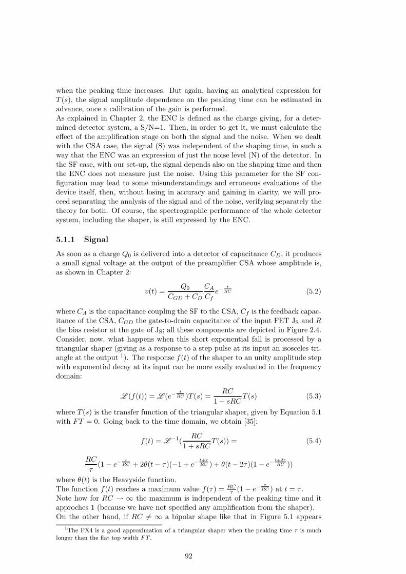
when the peaking time increases. But again, having an analytical expression forT (s), the signal amplitude dependence on the peaking time can be estimated inadvance, once a calibration of the gain is performed.As explained in Chapter 2, the ENC is defined as the charge giving, for a deter-mined detector system, a S/N=1. Then, in order to get it, we must calculate theeffect of the amplification stage on both the signal and the noise. When we dealtwith the CSA case, the signal (S) was independent of the shaping time, in such away that the ENC was an expression of just the noise level (N) of the detector. Inthe SF case, with our set-up, the signal depends also on the shaping time and thenthe ENC does not measure just the noise. Using this parameter for the SF con-figuration may lead to some misunderstandings and erroneous evaluations of thedevice itself, then, without losing in accuracy and gaining in clarity, we will pro-ceed separating the analysis of the signal and of the noise, verifying separately thetheory for both. Of course, the spectrographic performance of the whole detectorsystem, including the shaper, is still expressed by the ENC.
5.1.1 Signal
As soon as a charge Q0 is delivered into a detector of capacitance CD, it producesa small signal voltage at the output of the preamplifier CSA whose amplitude is,as shown in Chapter 2:
v(t) =Q0
CGD + CD
CA
Cfe−
tRC (5.2)
where CA is the capacitance coupling the SF to the CSA, Cf is the feedback capac-itance of the CSA, CGD the gate-to-drain capacitance of the input FET JS and Rthe bias resistor at the gate of JS; all these components are depicted in Figure 2.4.Consider, now, what happens when this short exponential fall is processed by atriangular shaper (giving as a response to a step pulse at its input an isosceles tri-angle at the output 1). The response f(t) of the shaper to an unity amplitude stepwith exponential decay at its input can be more easily evaluated in the frequencydomain:
L (f(t)) = L (e−t
RC )T (s) =RC
1 + sRCT (s) (5.3)
where T (s) is the transfer function of the triangular shaper, given by Equation 5.1with FT = 0. Going back to the time domain, we obtain [35]:
f(t) = L−1(
RC
1 + sRCT (s)) = (5.4)
RC
τ(1 − e−
tRC + 2θ(t − τ)(−1 + e−
t+τRC ) + θ(t − 2τ)(1 − e−
t+2τRC ))
where θ(t) is the Heavyside function.The function f(t) reaches a maximum value f(τ) = RC
τ (1 − e−τ
RC ) at t = τ .Note how for RC → ∞ the maximum is independent of the peaking time and itapproches 1 (because we have not specified any amplification from the shaper).On the other hand, if RC 6= ∞ a bipolar shape like that in Figure 5.1 appears
1The PX4 is a good approximation of a triangular shaper when the peaking time τ is muchlonger than the flat top width FT .
92

0 100µ 200µ 300µ-15m
-10m
-5m
0
5m
10m
15m
ampl
itude
(V)
time (s)
64 s
Figure 5.1: Signal processed by the PX4 shaper with peaking time set to 64 µs.The input signal is an exponential fall with decay time 18µs, i.e. the output of thePIN 1 detector. The signal is acquired by a digital scope and the noise is averagedout over many identical waveforms.
on the scope. In this figure a real signal obtained with τ > RC (τ = 64 µs andRC = 18 µs) is shown, confirming the correctness of the expression 5.4.
Note how in Figure 5.1 the leading and falling edges follow exponential laws,as expected from formula 5.4, with time constants equal to the decay time of theinput signal.
In the case of trapezoidal shaping, expression 5.4 becomes more complicatedand more terms appear in the equation; but for what concerns us nothing changes:the maximum is again at t = τ and has the same value. This maximum value ofthe output signal is detected by the PX4 and acquired as the final result of thesignal processing.Injecting a constant charge into the detector, a different amplitude is acquired,depending on the peaking time, proportional to:
RC
τ(1 − e−
τRC ) (5.5)
To verify this point, an 241Am spectrum has been acquired for several values of thepeaking time: the 60 keV peak position agrees with 5.5, as shown in Figure 5.2.Fitting the curve, it is possible to have a further determination of the parameterRC, that could be estimated or by static measurements or, more accurately, byfitting the output signal as seen on a scope, like the one of Figure 5.1. Moreover,it is a way to calibrate the gain of the whole acquisition chain, necessary to scalethe noise data. The expected amplitude of the signal is (in channels):
RC
τ(1 − e−
τRC )
Q0
CD + CGD
CA
CfA (5.6)
93

0 5 10 15 20100
150
200
250
chan
nels
peaking time ( s)
60 keV
Figure 5.2: Position of the 60 keV X-ray peak acquired with the PIN 2 detector.The solid line is calculated with expression 5.5, scaled by the gain.
product of the first in expression 5.4 with the amplification introduced by detectorand CSA and with the gain A of the shaper (in channels/V), the aim of ourcalibration.For every device, the 60 keV peak position has been measured versus peaking time,in order to determine the gain CA
CfA.
5.1.2 Noise
In chapter 2, the contribution of every noise source was calculated and expressedin terms of the ENC. There, it was understood that the signal amplitude is inde-pendent of the peaking time. As explained in the previous section, this is not thecase with our set-up.Since both signal and noise change with peaking time, this parameter is misleadingand we must calculate the theoretical σ2 of the noise in some arbitrary units (forexample, in channels of PX4) and compare it with the measured one, as we didfor the signal. The contributions of every type of noise (flicker, series or parallel)are calculated solving the integral and scaling it for the gain of the amplificationchain:
σ2 = A2
∫
∞
0dω
dv2out
df|T (iω)|2 (5.7)
wheredv2
outdf is the noise voltage power spectral density at the output of the CSA.
The single contributions are then, making explicit the gain parameter ACACf
:
- series:
σ2s = (
CA
CfA)2
1
τ(dv2
s
df+
dv21
df(CA + Cin
CA)2) (5.8)
94

- flicker:
σ2f = (
CA
CfA)2(Af,S + Af,1(
CA + Cin
CA)2) (5.9)
- parallel: as seen in chapter 2, the discharging of the signal through the de-tector RC leads to a non trivial calculation of the noise. There, this integralhas been calculated for a triangular shaper; in the case of a trapezoidal one,the integral I becomes:
I =
∫
∞
0dx
(1 − cos(x))(1 − cos(x(1 + FTτ )))
x2(1 + (xa)2)(5.10)
I =π
2+
aπ
4(−2 + 2e−
1a + 2e−
1a(1+ F T
τ) − e−
1a(2+ F T
τ) − e−
F Taτ ) (5.11)
with a = RCτ , and it is easily verified that for FT = 0 we are back to the
expression 2.59 of the triangular shaper. The parallel noise contribution canbe written as:
σ2parallel = (
CA
CfA)2
di2pdf
2R2
πτI (5.12)
The parameters of the detector, CD+CGD and R, enter only via the constanta.
Summing in quadrature these three independent terms, we get the total value ofσ2. Having established the required noise expressions, we began the study fromthe simplest devices, i.e. the pixels, in order to check our theoretical model.
5.2 Noise on integrated JFETs
The noise properties of the JFETs having, as bottom gate, one of the two p-wellsof Figure 1.15 have been explored by measuring the gate referred noise voltageby means of a spectrum analyzer [36], then in the frequency domain. As can beseen in Figure 5.3, the improvement achieved with the “new” p-well is significant:both the high frequency plateau, coming from white noise contributions, and the1/f noise are much better in devices built with the new technology. The 1/fnoise corner is as low as 100 Hz and the related noise coefficient Af , entering intonoise expressions for the ENC, is less than 10−13V 2, which can be neglected. Forcomparison, the Af parameter for the 2SK152 JFET used at the input of theA250 preamplifier is ten times greater. The white noise contribution is seen toscale correctly with the transconductance (not shown in the figure); however, it isquite high, due to the series resistance of those portions of the p-type implants ofboth the top gate and the bottom gate that are not covered by the metallization.The value of this gate resistance is of the order of 400 Ω. For the old p-well, whichis less doped than the new one, this gate resistance is even larger, as can be easilyappreciated from the high frequency part of the spectrum in Figure 5.3.All devices considered in the following have the “new” p-well.In the polarization range adopted, the gate leakage current is negligible, so thenoise coming from the JFETs is uniquely due to the gate resistance and to thechannel conductance. It can be expressed as a gate referred noise voltage powerspectral density:
dv2
df= 4kT (
Γ
gm+ RGate) (5.13)
95

100 1k 10k 100k1
10
100
nois
e vo
ltage
spe
ctrum
(nV/H
z0.5 )
f (Hz)
old p-well new p-well
Figure 5.3: Gate referred square root of noise voltage power spectral densities oftwo JFETs fabricated with the two different p-wells. JFET under measure is thetriode 1000/4, VS = 0 V, VD = 3 V and ID = 250 µA [36].
5.3 Measurements on Pixels
As anticipated in chapter 1, we have two kinds of pixels, named PIN 1 and PIN 2.The two pixel types have the same sensor size, then they have the same value forCD = 1.0 pF. They also have the same value of Rbias ∼ 3 MΩ, but they differ intheir JFETs:
- PIN 1 has JS of type 1000/4, i.e. having a channel length of 4 µm andchannel width of 1000 µm with CGD = 4.6 pF; JC, the current source FET,has a 400/4 geometry;
- PIN 2 has a 400/4 JS with CGD = 1.8 pF and a 200/4 JC .
The chosen values of power supply voltages must ensure the JFETs are working inthe saturation region, in order to get a good Source-Follower action. The chosenvoltages are VDD = 3 V, VSS = −3 V, VGG → ground and Vbias = 50 V (seeFigure 2.4), sufficient to deplete the 300 µm substrate. Both VDD and VSS areprovided by batteries, since the S and D currents in the mA range are not easilyfiltered by simple RC low-pass filters. In this condition the transconductance ofthe JFETs and the gate-drain capacitance CGD of JS are readily obtained fromtheir static characterization, described in Chapter 1:
- PIN 1: gm,JS= 10.7 mS, gm,JC
= 5.8 mS, CGD,JS= 4.6 pF
- PIN 2: gm,JS= 4.6 mS (gm,JC
is not measurable, since the gate is short-circuited to the source, and no test-structure of this size is present on thewafer), CGD,JS
= 1.8 pF.
96

parameters for PIN 1
CA (pF) Rbias (MΩ) C parasitic (pF) fitted τ (µs)
none 2.65 1.2 17.98 2.70 0.6 17.167 2.75 0.8 17.5
1 nF 2.75 1 18
Table 5.1: Summary of some of the parameters fitting the data acquired withthe pixel PIN 1. First line (output of the SF directly connected to PX4, withoutcapacitor CA) refers to Figure 5.4, second line to Figure 5.5. The fitted τ valuesare derived from curves analogous to the one shown in Figure 5.2.
The transconductance and capacitance values above reported are measured on teststructure devices, since in pixel detectors with source-follower not all terminals areaccessible. For example, the gate of JS is not accessible and the source and gateof JC cannot be independently contacted. The quoted values must be taken asapproximate, since a spreading of the parameters has been observed in test struc-tures.Since the leakage current is very low, few tens of pA, the voltage drop on the 3 MΩbias resistor is negligible and the gate stays practically at the same voltage of VGG,i.e. ground.At the drain of JC (connected to the source of JS), a pad allows the connectionof an external capacitor CA of selectable value. Direct connection to PX4 input isalso possible; in this case the input signals are very small, fractions of a millivolt.This option, however, has been explored and found to give acceptable results.As explained in previous sections, we expect the product of Rbias with CD + CGD,symbolized by RC, to be equal to the time constant of the exponential decay ofthe output signal, recorded by a digital scope.What we observe in every detector is that the DC value of polysilicon resistormultiplied by the measured capacitance is slightly greater then the decay time ofthe output pulses.For PIN 1 this product is 18.5 µs and the decay time fitted on the signal shape is∼ 18 µs; for PIN 2 the RC product is 9.9 µs against a fitted decay time of ∼ 9.0 µs.We expect the other way around, since parasitic capacitances are likely present.This 5-10 % discrepancy could be attributed to the fact that the bias resistor seesunder the oxide a further resistance on the undepleted substrate: the oxide capac-itance, in the frequency range of interest, shorts the two resistances. In this way,the effective resistance is the parallel of the two. Even though we could expectsome kind of frequency dependence, throughout the noise calculations a constantresistance for every peaking time is used. Measurements made on both pixels jus-tify this first order approximation. Capacitances of some fractions of picofarad,accounting for parasitics, are added to fit the experimental data. The product ofthe “effective” resistance and the “corrected” capacitance is, with good approxi-mation, equal to the time constant derived by fitting the 60 keV data similar tothose in figure 5.2. In the two tables 5.1 and 5.2, a summary of the parametervalues used for the two pixel types is presented. The noise data in Figure 5.4,plotted together with the theoretical curves expected from the parameters listed intables 5.1 and 5.2, refer to the SF directly connected to the PX4 shaper, without
97

parameters for PIN 2
CA (pF) Rbias (MΩ) C parasitic (pF) fitted τ (µs)
none 2.65 0.5 9.167 2.65 0.4 9.0
Table 5.2: Summary of some of the parameters fitting the data acquired with thepixel PIN 2. First line refers to Fig. 5.4 and line 2 to Figure 5.5.
interposing the CSA. In this case, the noise contribution of the A250 is replacedby the input noise of the PX4. In the plots, it is parameterized with a series re-sistance of 1 kΩ, which is exactly its input impedance [37]; expected noise, as canbe seen, is smaller than the measured one at the lowest peaking times, while athigher peaking times, when the thermal noise of the 3 MΩ bias resistor on the pixeldominates, the agreement is good. Flicker noise from PX4 may be responsible forthis discrepancy.Of course, the Johnson noise of the 3 MΩ resistor is dominant over other noisesources. It behaves as parallel noise until peaking times of the order 2 RC; beyondthat point, it shows a series noise behavior. This is more evident on PIN 2 pixel,exhibiting a shorter RC time constant.One could think about increasing Rbias by connecting an external resistor in serieswith the 3 MΩ integrated resistor, in order to reduce the parallel noise; howeverthis would be ineffective because the output pad of the 3 MΩ resistor has a largecapacitance to the undepleted substrate, effectively shorting it to ground in thefrequency range of interest.At low peaking times, the series noise contribution from the gate resistance be-comes important. For both devices, a value of 400 Ω can be deduced from the mea-sured noise versus peaking time dependence. Another group measured [19] [36],by means of a spectrum analyzer, the noise power spectral density (shown inFigure 1.15) of the JFETs making up the SF, finding good agreement with ourmeasurements in the time domain. Such a high value for the series resistance isdue to the resistance of the long and narrow gate implants.Figure 5.5 shows the plots acquired from the two PIN devices, AC-coupled to theCSA through CA. In this case, we can neglect the noise coming from the last am-plification stage (the PX4) and, again, the noise is well reproduced by calculations.With the source-follower, the test capacitance present on the preamplifier board
cannot be used to inject charge into the detector. Moreover, the pixels do nothave a DC pad for connecting an external Ctest to the detector. The only way togenerate events is irradiating the detector with some kind of particle. Acquisitionof 241Am spectra is not practical because it requires a long time (due to the smallarea of the pixels) and the 60 keV peak is not well separated from the backgroundespecially at high peaking times, where the system is noisier. The most convenientway is illuminating the sensor with short pulses from a LED, whose statistics ofphoton emission should not contribute appreciably to the noise. Data for the pixeldevices are generated with this method.
98

1 105
10
15
20
25
30
FWHM
(cha
nnel
s)
peaking time ( s)
PIN 1 PIN 2
Figure 5.4: Scan of the FWHM noise (expressed in ADC channels) versus peakingtime on devices PIN 1 and PIN 2, with output directly connected to PX4. Con-tinuous lines are calculated with the measured parameter values. The gains of theamplification stage are different, so a comparative discussion of the noise in thetwo pixels is not possible at this level.
5.4 Measurements on Strip Detectors
The detector includes a Source-Follower at the end of each strip. The strip isDC coupled to the gate of the input JFET JS of the SF. Since the strips are alsoprovided with bonding pads, we have two different options for signal readout:
- CSA configuration, in which the strip is AC-coupled to the A250 preamplifierthrough an external capacitor;
- SF configuration, in which the output of the SF is AC-coupled to the A250through a capacitor integrated on the detector wafer (this how the detectorwas intended to be operated).
In the following we discuss separately the two cases.
5.4.1 CSA Readout
An external 2 nF capacitor AC couples the strip to the input of the CSA. With ref-erence to Figure 1.17(b), VDD is set (by batteries) to 2.5 V, while VSS and VGG areat ground. In this way the strip is biased through the 4R voltage divider at VDD/2,with an effective bias resistance of value R, which has been measured to be 0.8 MΩ.In these conditions, JS is biased just barely into saturation; for good SF operation,a higher value of VDD would be preferred, but here the SF is not used. For whatconcerns the noise, the effect of the SF is just to add the gate-drain capacitanceof JS to the input node of the CSA. The well calibrated 2.28 pF Ctest mounted on
99

1 10
15
20
25
30
35
40
FWHM
(cha
nnel
s)
peaking time ( s)
PIN 1 PIN 2
Figure 5.5: Scan of the FWHM noise versus peaking time on devices PIN 1 andPIN 2, connected to the A250 with capacitances of 8 and 67 pF respectively. Asin Figure 5.4, the gains are different for the two curves, so the vertical scale doesnot have an absolute meaning.
the CSA board can be conveniently used to inject a charge signal into the detector.
We have two choices for the dealing with the neighboring strips:
- short the neighboring strips to ground for the signal, by connecting a largevalue capacitor between their DC pad and ground; in DC, all the strip remainbiased at the same voltage, set by the resistive voltage divider;
- leave the neighboring strips “floating” in AC, i.e. biased only through thevoltage divider, with an effective resistance to ground of ∼0.8 MΩ.
Noise measurements versus peaking time taken in both configurations are shownin Figure 5.7.
Neighbors grounded
Keeping the DC pads of the neighboring strips at ground (for the signal), wehave again the standard configuration of a capacitive detector read out by theCSA, described in Chapter 4. Here the noise from nearby strips (due to their biasresistors and leakage currents) is not coupled, via the interstrip capacitance, to thestrip under measure, but is shorted to ground. The capacitance seen by the inputof CSA is the sum of the capacitances to the backside, to the bias ring, and tothe adjacent strips (which we lump together under the symbol CD), plus the gate-drain capacitance of JS. The measured noise, because of the large parallel noise
100

Rbias Cbulk
single strip
A
Cis
Figure 5.6: Schematic of the strip detector as used in the SPICE simulations.Every strip is represented by a capacitance towards the backside, in parallel witha bias resistance, plus a capacitance towards the neighboring strips. Values of theparameters are: Rbias =0.75 MΩ, Cis =7 pF, Cbulk =9 pF. In the case shown, anammeter measures the noise current. If we are interested in measuring a noisevoltage, a voltmeter replaces the ammeter.
contribution from Rbias, is not much sensitive to series noise and then to totalcapacitance. From the data of Figure 5.7 a total input capacitance of roughly36 pF can be estimated; by subtracting the well known Cin of the CSA (13 pF),we get CD +CGD ∼ 23 pF. From the same noise data we can instead obtain a goodmeasure of the effective bias resistance, which is found to be 0.75 MΩ, slightly lessthan the DC measured value.
Neighbors floating
The strips are polarized by the 4R voltage divider; in AC, they see an effective biasresistance to ground given by 2R||2R = 0.75 MΩ. In this condition the noise ofthe other strips (dominated by the contribution of their bias resistance) is coupledvia interstrip capacitances to the strip under measure.In order to estimate this noise we must solve a network of resistors and capaci-tors, representing the strips of the detector. Since the analytical solution is notsimple, we analyzed the circuit shown in Figure 5.6 with the help of a SPICEcircuit simulator [38]. A strip is represented by the parallel of a capacitance and aresistance towards ground with two interstrip capacitances towards the neighbor-ing strips. The resistance has the value determined from the noise measurementwith neighboring strips at ground in AC. For the interstrip capacitance we use thevalue (7 pF) obtained from direct measurements; in order to sum up to 23 pF aspreviously estimated for the CD + CGD capacitance, the capacitance to ground inthe network of Figure 5.6 must be ∼ (23 − 2 × 7)pF = ∼9 pF.
The simulator adds in series to each resistor its noise voltage source dv2
df = 4kTRbias
or, in parallel, its Thevenin equivalent di2
df = 4kTRbias
. Since we are interested in acurrent noise, an ammeter is used to read it.The resulting noise current spectral density at the CSA input, in the frequencyrange of interest (5 to 500 kHz), can be fitted as:
√
di2ndf
= 1.72 − 0.236
1 + ( f14.14 kHz)
1.77(10−13 A√
Hz) (5.14)
101
1 10500.0
1.0k
1.5k
2.0k
2.5k
3.0k
3.5k
neighbor floating neighbor grounded
EN
C
peaking time ( s)
Figure 5.7: Noise measurements on strip detector with the strip AC-coupled to theCSA, bypassing the integrated SF stage. The JFETs are polarized with VDD =2.5 V and VSS = 0 V. With neighboring strips grounded, the model used inChapter 4 can be directly applied; with the strips floating (actually, connectedto ground by a 0.75 MΩ effective resistance), a numerical calculation must beperformed in order to estimate the expected ENC.
The contribution of this noise at the output of the shaper has been determined bynumerically calculating the integral:
ENC2parallel =
∫
∞
0dω
di2ndf
|T (ω)|2ω2
(5.15)
where |T (ω)|2 depends on the trapezoidal shaping parameters τ and FT (equa-tion 3.3).This term is just the contribution of the parallel noise of the detector. We mustadd in quadrature other noise terms like the series noise of the CSA input FETand the 1/f noise. The result is shown as a continuous line in Figure 5.7, togetherwith the measured experimental points.It can be seen from the plot that, by increasing the peaking time (i.e. going tolow frequencies), the relative difference between the two curves decreases; thishappens because the impedance of Cis increases at low frequency, cutting off thenoise current originating from the other strips. This can also be seen from equa-
tion 5.14: in the low frequency limit the noise reduces to just√
di2
df =√
4kTRbias
, with
Rbias =0.75 MΩ, i.e. the contribution of the resistance biasing the strip under test.
5.4.2 Readout with Source-Follower
This is the way these strips were intended to be used: taking the signal from theoutput of the SF through the integrated coupling capacitor CA (Figure 1.17(b)).
102

1 10 100
15.0
17.5
20.0
22.5
25.0
FWHM
peaking time ( s)
SF - neighbor grounded
Figure 5.8: Noise measurement on strip detector taking the signal from the in-tegrated CA, after the SF stage. C = 26 pF, RS = 500 Ω, Rbias = 0.75 MΩ.Neighbor strip are grounded, so we fall in the case of the previously seen pixels.
Due to space limitations on the wafer, the value of CA is only 22 pF, slightly lessthan the capacitance CD + CGD seen by the gate of JS. VDD is set by batteriesto 3 V, while VSS = VGG = 0. The strips are biased at VDD/2 =1.5 V. Staticcharacterization of the SF has shown that this is a convenient working point. Theparameters of JS entering into noise expressions cannot be directly measured on thedevices connected to the strips, because its source terminal is not externally accessi-ble; however, devices with the same layout are included in test structures and havebeen characterized (Chapter 1). We obtained: gm,JS
= 1.0 mS, CGD = 3.0 pF.The JFET JC has gate and source connected together, making it impossible tomeasure the transconductance; since no test structure with the same geometryexists on the wafer, we can only rely on scaling considerations.The bonding pad present on every strip can be exploited to inject a signal chargethrough an external 1 pF capacitor Ctest (properly terminated with 50 Ω toground).Again, we can choose to leave the adjacent strips floating, or clamp them to GNDwith a large capacitor.
Neighbors grounded
In this configuration, we are back to the case of the pixels, since the nearby stripsdo not contribute to the noise. By acquiring the signal waveform at the outputof the CSA with a digital oscilloscope, we could determine its decay time, whichreproduces the decay time of the voltage signal on the strip. From this we canget a good estimate of CD + CGD + Ctest, since R is well determined by previousmeasurements with CSA read-out. The decay time is 18.8 µs. Then, given the
103

1 10 100
16
18
20
22
24
26
28
FWHM
(cha
nnel
s)
peaking time ( s)
Figure 5.9: Noise measurement on strip detector taking the signal from the in-tegrated CA, after SF stage. Neighbors strips are floating, as in the expectedSF configuration. Numerically calculated curve comes from integration 5.19, withnoise voltage expression given by a SPICE simulation of the model of Figure 5.6,with the same parameters used in Figure 5.7.
value Rbias = 0.75 MΩ, a total capacitance of 25 pF (1 pF out of these 25 pF isdue to Ctest) can be deduced.The calibration of the charge injection at the input is not straightforward: thenoise of these structures is indeed high, given the low value of the bias resistor. Asa result, the 60 keV X-ray peak is not well separated from the noise and is clearlyvisible only at the lowest peaking times.Moreover, the injected charge depends on the ratio of Ctest to the total capacitanceof the detector node (input of the SF). Indeed, because of the high input impedanceof the SF, the strip is not kept at virtual ground as it was with CSA readout, sothe real injected charge is not simply Q0 = Ctestvin, but less, depending on thevoltage divider built-up by the capacitances Ctest= 1 pF and CD + CGD= 24 pF:
Q0 = Ctest(vin − vstrip) = Ctestvin(1 −1
24pF1
24pF + 11pF
) (5.16)
where vin is the square wave amplitude applied to Ctest.Comparing the signal pulse height generated by Q0 with the one due to the 16.6 kereleased by the 60 keV photons we can, as in the case of the pixel, determine thegain of the whole system.The measured noise data are shown in Figure 5.8 together with the expected ones,where a further 1 pF is added to the total capacitance in order to better fit thedata.
104

Neighbors floating
In this configuration, predicting the noise level is rather difficult and we cannot givean accurate analytical expression for it. It is similar to the case shown in Figure 5.7,in which the signal is taken from the DC pad while the neighboring strips remainfloating. As in that case, we must rely on SPICE simulations. Referring back tothe sketch shown in Figure 5.6, the ammeter must be replaced by a voltmeter,since we are sensing a noise voltage 2. With the same parameter values of theprevious simulation, the output expression for the noise voltage spectral densityis:
√
dv2
df=
1.1510−7
1 + ( f19.25 kHz )1.24
V√Hz
(5.17)
for frequencies ranging from DC to 70 kHz and:√
dv2
df= 1.1810−3f−0.983 V√
Hz(5.18)
for frequencies from 70 kHz to 10 MHz.At low frequency, where Cis, coupling the strip under test to its neighbors, hasa high impedance, the noise is dominated by the bias resistor of the strip itself
(√
dv2
df =√
4kTRbias). At high frequency, the interstrip capacitances are shorted
and the noise voltage at the SF input is generated by the parallel combination ofmany bias resistors, giving a lower level of voltage noise.The r.m.s. noise at the output of the shaper can be obtained from the noisevoltage spectral density given above at the SF input, by numerically evaluatingthe integral:
σ2 = (ACA
Cf)2
∫
∞
0dω
dv2
df|T (ω)|2 (5.19)
The gain term, expressed by the product ACACf
, has been determined from the
previous measurement with neighbors grounded. The set up, indeed, has been keptidentical in the two configurations, apart from the removal of the 2 nF capacitancesbetween the DC pads of the adjacent strips and ground.The agreement, as can be seen in Figure 5.9, is not at the level of the previouscase (Figure 5.8). Anyway, the general behavior is reproduced.
The waveform in this latter case is worth a separate discussion. It is not asimple exponential decay: the injection of a charge into a strip initially rises it to apotential: vhit,0 = Q0
C′ , where C ′ is the capacitance between the strip, connected tothe gate of JS, and all other electrodes kept at constant voltage (at ground in AC).Contrary to the previous case, the other strips are not grounded and they chargeup through the voltage divider given by the interstrip capacitance Cis and theirown C ′. Referring to Figure 5.10, and calling vnear the voltage of the adjacentstrip, we expect at time zero:
vhit,0 =Q0
C ′(5.20)
vnear,0 =Q0
C ′
Cis
Cis + C ′(5.21)
2This is due to the high input impedance of the SF. By contrast, the low input impedanceCSA was sensitive to the noise current.
105

RbiasRbias
isCnearv vhit
C C
Figure 5.10: Sketch of two nearby strips for the calculation of waveforms generatedby a charge released in one of the strips.
In this way, the signal spreads from one strip to the nearby ones, a so called cross-talk effect. An analogous argument holds for the other nearby strips, but, sincethe voltage divider is made up by more capacitances as we move away from thehit strip, the signal on those strips is expected to be smaller. Moreover, since justone strip is actually collecting the charge, the pulses from the other strips musthave a bipolar shape with zero area. An example of acquired pulses is shown inFigure 5.11. To calculate the time dependence of the signal for the very schematiclayout of Figure 5.10, we must solve the two differential equations expressing theKirchhoff current law for the two strip nodes:
vnearR + C dvnear
dt + Cisd(vnear−vhit)
dt = 0vhitR + C dvhit
dt + Cisd(vhit−vnear)
dt = 0(5.22)
The simplest way to solve the system is through a Laplace transform, but thecalculation quickly diverges in complexity. A first order approximation that canbe done is to set C = Cis, translating in a simple relation between the zero-timepotentials of the two strips: vhit,0 = 2vnear,0. The signal from the hit strip is thenfound to be:
vhit(s) = 32vhit,0RC 1+s2RC
1+4sRC+3s2(RC)2
vhit(t) = 14vhit,0(3e
−t
RC + e−t
3RC )(5.23)
whose time integral is∫
vhit(t)dt = 32RCvhit,0. The solution is the sum of two
exponential decays, with time constants RC and 3RC; in the more general caseof Cis 6= C, the two time constant are RC and RC + 2RCis. The signal from theneighboring strip is:
vnear(s) = 32vhit,0RC sRC
1+4sRC+3s2(RC)2
vnear(t) = 14vhit,0(3e
−t
RC − e−t
3RC )(5.24)
very similar to the previous one, but with a “-” sign, leading to a null integral.The time constants are the same.If we inject a charge in the detector with a light pulse from an LED instead ofusing the Ctest, nearly the same charge is injected on every strip, so they all chargeup at the same voltage. As a result, the interstrip capacitances Cis do not chargeup. The resulting waveform is the same on every strip: it is a single exponentialdecay, with a time constant much shorter with respect to the case of injectionthrough Ctest. This is due to the fact that the effective strip capacitance is much
106
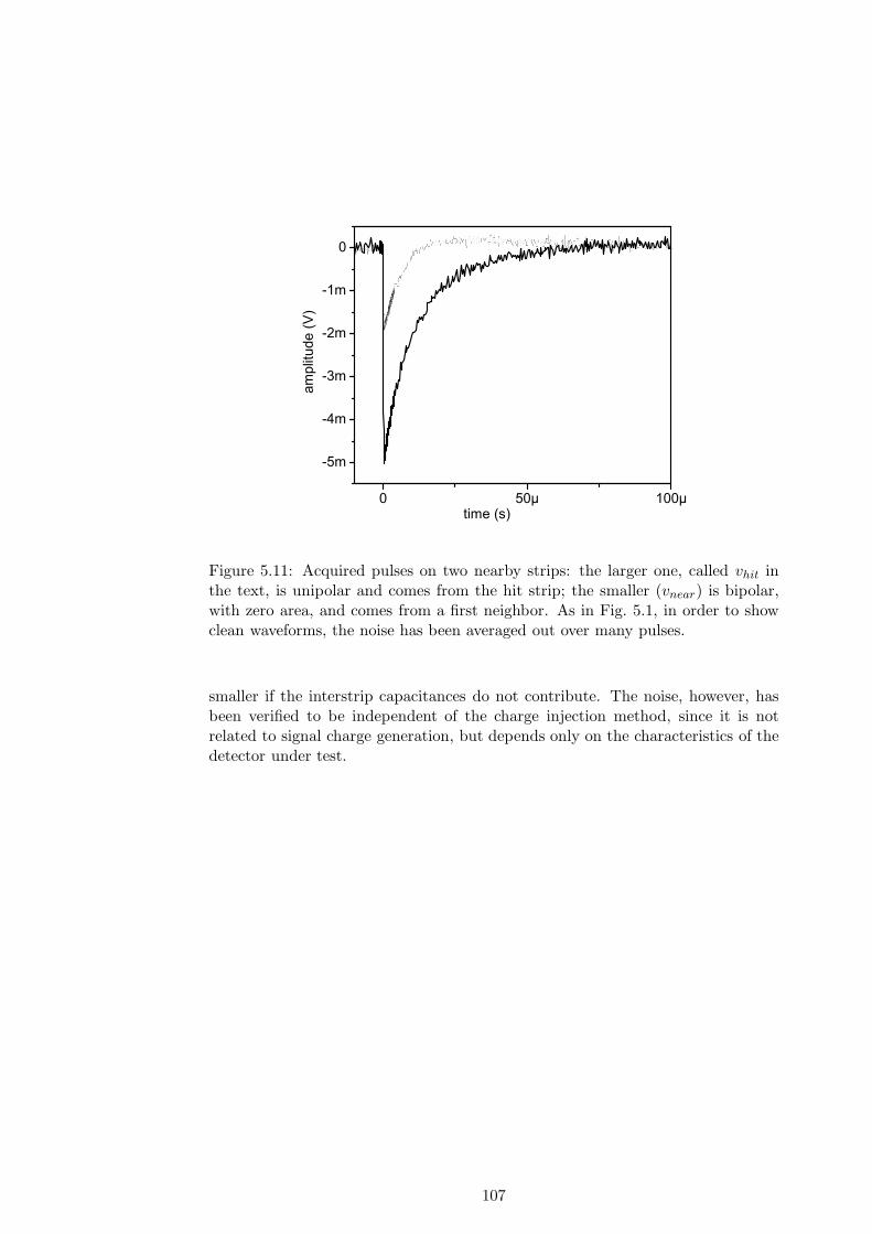
0 50µ 100µ
-5m
-4m
-3m
-2m
-1m
0
ampl
itude
(V)
time (s)
Figure 5.11: Acquired pulses on two nearby strips: the larger one, called vhit inthe text, is unipolar and comes from the hit strip; the smaller (vnear) is bipolar,with zero area, and comes from a first neighbor. As in Fig. 5.1, in order to showclean waveforms, the noise has been averaged out over many pulses.
smaller if the interstrip capacitances do not contribute. The noise, however, hasbeen verified to be independent of the charge injection method, since it is notrelated to signal charge generation, but depends only on the characteristics of thedetector under test.
107

108

Chapter 6
Comparative Discussion of the
Experimental results on CSA
and SF
An experimental comparison of SF vs CSA read-out methods has been alreadycarried on in [39]. In that work, a low capacitance detector, used for X-ray spec-troscopy, had the first JFET of the front-end electronics integrated on the samesilicon substrate of the detector, and served as input device for both the SF andCSA readout configurations. All the other components of the amplifier have beenplaced outside the chip. The reset of the signal and leakage current charge wasachieved by means of both pulsed and continuous methods, avoiding the Rbias andits thermal noise. It was pointed out that, considering null noise contribution ofthe external amplifier, the S/N performances should be equal for the two read-out methods, since the noise sources, as long as the FET is made working at thesame biasing point, are the same and the amplification affects in the same man-ner both signal and noise. We add that, since the CGS capacitance of the inputFET does not contribute in the SF, SF could be even better. However, the papershows that with the SF a much poorer linearity is achieved than with the CSA:with the latter, the output voltage of the preamplifier is directly linked to thesignal charge via the feedback capacitance, a very stable parameter, whereas theSF links just the output voltage with the gate voltage of the first JFET, withoutmaking a precise conversion in advance between the input voltage and the signalcharge. This relationship depends on the capacitance at the input node (sum ofCD, CGD and strays) and for spectroscopic detectors (having small capacitance),significant variations with detector and FET bias are expected (and observed).Variations with temperature are observed too to be much more severe in SF thanin CSA read-out. It may be stated that in an environment with controlled biasand temperature their performances are at the same level. However, it is not thecase: the signal and leakage currents are integrated at the input node, shifting thepolarization point of the FET and then its capacitances. In the SF, this causes avariation of the gain with a broadening effect of X-ray lines, similar to the effectof the noise.Particular care should be taken in the choice of the reset method. A pulsed re-set method, removing the charge only at fixed time intervals, should be avoidedbecause then pulses arriving at different times are amplified at different levels. A
109

1 1010
20
30
40
50
FWHM
(cha
nnel
s)
peaking time ( s)
SF CSA
Figure 6.1: Plots of the measured FWHM noise for the PIN 1 (upper curve) andPIN 2 devices; also shown the expected noise with CSA read-out (with the samepixel parameters).
continuous reset, as a diode in parallel to the detector, is to be preferred, allowingcurrents from the detector to flow through its forward biased junction, whose po-tential drop is set by the amount of current.In our devices, even if a parasitic diode could be a viable alternative, a polysiliconRbias was chosen as a path to the currents, because of its simplicity. The noiseperformances, of JCcourse, worsen. Static characterizations on FETs showed aspreading in the values of capacitances, so the gain is expected to vary from stripto strip. This issue is absent in the CSA read-out method, since the gain dependsonly on the well determined parameter Cf , in every case external to the detectorchip. In a severe environment like a collider, a continuous calibration of the ca-pacitance (measuring the gain) should be performed, but this is impractical.Already these considerations on the signal make the classic CSA a better choice:but let’s consider other features of the two readout configurations.
In the following analysis, we concentrate on noise issues.In Chapter 2, when comparing the SF with the CSA, we made some crude approx-imations:
1 - CGD, the capacitance of gate-drain junction of the input JFET of the SF, isnegligible with respect to the detector capacitance CD;
2 - RS and Af (the flicker noise coefficient) are negligible for the input transistorof the SF;
3 - Af,1 of the input FET of the CSA is zero;
4 - the JFET current source JC is noiseless.
110

Contrary to what done in [39], the noise coming from the external amplifier hasbeen taken into account.Approximation # 3 has been introduced to simplify the calculations, leading toa simple relation between the transconductances of JS and J1, derived in equa-tion 2.70; obviously it does not hold in real situation, and in our case the coefficiententering noise expressions is a well determined parameter with value 1.6 10−12 V2.Approximation #2 refers to an ideal low-noise JFET, fabricated for spectroscopicapplications. The flicker noise coefficient on our integrated JS and JC JFETs are,as measured, really negligible, less than 10% of the noise of 2SK152; RS , on theother hand, is very large, ∼ 400 Ω, due to some design limitations.Approximation # 4 is a good one, since the noise term coming from JC can bemade smaller than the noise term of JS :
4kTΓgm,C
g2m,S
< 4kTΓ1
gm,S(6.1)
To discuss properly item # 1, it is better to go in deeper detail, splitting thedevices studied in high and low value capacitance: namely strips and pixels.As usual, we start from the pixels.
6.1 Pixels
The PX4 digital filter is not able to shape correctly input exponential falls withtime constant less than 36 µs, as is the case of our pixels. A signal pulse heightdeficit, function of the peaking time, will occur. This is not the case with the CSA,whose long decay time comes from the product RfCf of the feedback path. Thesignal, then, is processed correctly, giving, independently of the peaking time, anunvarying signal amplitude at the output. In this condition, the CSA is betterthan the SF, from the point of view of the ENC, especially at long peaking times.In the following, we suppose to have the same signal for every peaking time, given,at the input of PX4, by Q0/Cf in the case of CSA and Q0
CD+CGD
CACf
in the SF
case. Figure 6.1 shows a summary of the experimental data taken from bothpixels, PIN 1 and PIN 2, already shown together in Figure 5.5. Also shown is theexpected value for a CSA configuration, that would be measured with the samegain of the whole acquisition set-up.Relation 2.70 gives, for the transconductance gm,S of JS of PIN 1, a minimum valueof 3 mS, with the CD and CA values used in this particular noise measurement. Inthe same way, for PIN 2, relation 2.70 gives a minimum value for gm,S of 0.4 mS.Both conditions are largely satisfied, so the fact that the noise in CSA is less thanthe noise in SF for PIN 1 for short peaking times - when series noise dominates -,must be due to some not well verified approximation, listed in item #1 through#4.Anyway, at longer peaking time, the CSA becomes much noisier than the SF, dueto the Johnson noise of the 3 MΩ resistance which starts contributing as seriesnoise in SF read-out, then giving a noise contribution decreasing with peakingtime. At high frequency (low peaking times), the 3 MΩ acts as a parallel noisesource, for both set-up. Its contribution to the total noise is the same for both SFand CSA read-out methods.Since parallel noise cannot explain the different behaviour of the two read-out
111

at low peaking times, this difference must then arise from series contributions,expressed below. Series contributions in the CSA case are proportional to :
(CD + Cin)
√
1
τ4kT (
Γ
gm,1+ RS,1) + Af,1 (6.2)
The numerical value of the square root, using the parameters of the used set-up,is 2.1 107 V2. For the SF:
(CD + CGD)CA + Cin
CA
√
1
τ4kT (
Γ
gm,1+ RS,1) + Af,1+ (6.3)
(CD + CGD)
√
1
τ4kT (
Γ
gm,S+ RS,S)
if the flicker noise of JS and the noise from JC are neglected.The numerical value inside the second square root is 4.7 107 V2, with the param-eters of the system.It is bigger because of the 400Ω of RS,S. Having fixed all parameters but thecapacitances, the condition for which the CSA is worse than the SF translate in arelation among them:
(CD + Cin) > (CD + CGD)CA + Cin
CA+ 1.5(CD + CGD) (6.4)
where 1.5 =√
2.1 107/√
4.7 107.Supposing that the above relation holds for both pixel types, and substituting theparameters CA = 8 pF or 67 pF, CD = 1 pF and Cin = 14 pF we get a conditionfor CGD.For CA = 8 pF, equal to the capacitance used in the PIN 1 measurement, CGD <2.5 pF for SF to be better than CSA: this condition is satisfied by PIN 2, havinga CGD = 1.8 pF but not by PIN 1 having CGD = 4.6 pF; this explains why in theFigure 6.1 PIN 1 has worse noise performances than CSA.CA = 67 pF, as used for PIN 2, sets the upper limit of CGD at 4.5 pF, then againSF is a better choice for PIN 2 (as seen in Figure 6.1) but for PIN 1 we need aneven bigger CA.In Figure 6.2, it is shown the maximum CGD, in function of CA, for which the
SF gives better noise performances than CSA.
6.2 Strip
The strips with integrated SF show several limitations, related to their particulardesign and also to some unavoidable intrinsic characteristics, making them unfitto be used for tracking purposes in high energy physics experiments.
Design Limitations
Some limitations belong to the specific detector under study and could be correctedwith a suitably modified design:
112

1 10 1000
1
2
3
4
5
C G
D (p
F)
CA (pF)
Figure 6.2: Plot of the maximum CGD of JS in function of the coupling capaci-tance CA, for which - theoretically, according to 6.4 - SF is better than CSA. Theparameters used are: CD = 1 pF, Cin = 14 pF, gm,1 = 13 mS, gm,S = 10 mS,Af,1 = 1.6 10−12 V2, RS = 400 Ω
- the integrated coupling capacitance CA is only of 22 pF, less than CD; inthis way, strips read by SF cannot hold a comparison with CSA read out,since the first condition for obtaining a better noise performance from theSF compared to the CSA the opposite condition: CA > CD.
- the small current, generated by JC, sets the VGS of JS to a value of −0.77 Vand to a small value for the transconductance gm,S . This makes series noisesignificant, as can be seen in Figure 5.9 or 5.8 where the minimum noise isachieved for 1.6 µs of peaking time, greater than the minimum allowed bythe shaper.
- the big value of series resistance, due to the incomplete metallization of thegate implant, increases the series noise too.
Intrinsic Limitations
Even though the JFETs of the SF draw a relatively low current, the power dissi-pation is ∼ 1 mW/channel (Idrain = 0.3 mA ·VDD = 3 V). This thermal budget isenterely produced inside the detector substrate, which would require to be cooled.Of course, the cooling of the CSA stage is also needed.Moreover, charge collected in one strip induces signals on the neighboring strips,giving a sizable cross-talk. This would help the signal interpolation of course;however, it leads to high occupancy, increased dead times and, possibly, eventlosses.
113
Conclusions
In this work, among all types of silicon detectors, we concentrate upon themicrostrip ones. The goal was, on one side, to investigate the noise sources inmicrostrip detectors – with particular attention to the contribution of the punch-through biasing mechanism – and on the other side to compare two different ap-proaches for the readout of signals: the classic charge sensitive amplifier (CSA)and a less common Source Follower (SF) integrated with the sensor as first ampli-fication stage.
The strip sensors read out by the CSA are of the type used in the Inner TrackingSystem of the ALICE experiment; they come in three different versions, suppliedby three manufacturers. The detectors with integrated SF are test devices designedfor evaluation purposes, in view of a possible utilization of this readout scheme inHigh Energy Physics experiments.
The study of both detector types started with a static characterization of thedevices, in order to verify their functionality and to measure the values of theparameters entering into noise expressions.
On the ALICE-type detectors, in addition to the standard tests performedto verify the quality of the sensors, some more detailed measurements have beenmade. In particular, the interstrip capacitance and related dissipation factor (tocomplete the information about the interstrip admittance) have been measured asa function of both frequency and bias voltage.We found that at bias voltages above substrate depletion both capacitance anddissipation factor still show a substantial dependence on frequency. Only at biasvoltages much above depletion this dependence flattens out.
This observed behaviour has been attributed to the presence of resistive layers,such as electron accumulation at the interface – or the p-spray implant in one sensortype – which at low frequency strongly couple one strip to the other strips of thedetector. At a sufficiently high bias voltage, the electron accumulation channels(but not the p-spray implant) in between the strips become insulated from eachother, because of the depletion of the narrow region between the strip end and thebias ring. Then the long-range coupling between the strips is no longer presentand the capacitance and dissipation factor become independent of frequency. Thispoint has been verified by 3D numerical simulations.
Detailed measurements of noise have been performed, exploring its dependenceupon a wide set of parameters: the diode polarization method (resistor or punch-through), the shaping time, the leakage and the punch-through currents, the de-tector bias voltage. Photogeneration and direct injection – through the DC padof the strip – has been used to vary over a wide interval the leakage and thepunch-through currents, independently of each other.
It has been found that the current flowing by punch-through contributes anadditional shot noise term, added in quadrature to the contribution of the leakagecurrent. This suggests that fluctuations in the two currents are uncorrelated, i.e.the arrival of carriers on the strip from the bulk is uncorrelated to their emis-sion towards the guard ring. Since the punch-through mechanism involves the“thermionic-like ” emission of carriers above a potential barrier, it is expected tobe subject to shot noise fluctuations, at least until space charge effects becomeimportant, smoothing out the fluctuations ([8], p. 221). However, if the fluctu-ations in punch-through current were (to consider the extreme case) completely
114

correlated to the fluctuations in leakage current, they would bring no additionalcontribution to the detector noise.
An unexpected noise contribution related to punch-through has been foundon the p-side of one type of sensors. Unlike shot noise, which is proportionalto the square root of current and shaping time, this new contribution is directlyproportional to both the punch-through current and the shaping time. Its power
spectral density can be described as a parallel flicker (1/f) noise: di2
df ∝ I2PTf .
A similar dependence of excess noise on the shaping time has been reported in theliterature [34],[33]. However, it has been observed only in irradiated detectors, andthe reported dependence on leakage current was the same as for normal shot noise,i.e. square root of I, while we observe a linear dependence, at least at moderatecurrent values.
The bias voltage, once the sensor is totally depleted, is not expected to havea significant influence on noise, the only effect being due to a slow decrease incapacitance. Instead, an extra noise contribution has been observed, which can beparameterized as a noise current power spectral density: di2
df ∝√
f .This excess noise is present precisely for those detectors and for those bias voltagesfor which the capacitance and dissipation factor were not flat versus frequency. Itis then natural to relate the origin of this noise to the presence of resistive lay-ers surrounding the strips. The physical mechanism responsible for this noise isnot clear. In the literature, an observed excess noise has been attributed to resis-tive lines (p-stops), and described in terms of thermal noise associated with theresistance, capacitively coupled to the adjacent strips [40]. However, this noisemechanism would be characterized by a frequency dependence completely differ-ent from the one we observed.
Our versatile measurement set-up began to show its limitations in the studyof detectors with integrated source follower.In this case, the output signals from the preamplifier have an exponential decaywith a time constant which is set by the RC constant of the detector. For therelatively low value of the bias resistors present in our devices, this time (∼20 µs)is too short to be correctly processed by the PX4 shaper.However, by using the known transfer function of the shaper we are still able toderive analytical expressions for both the noise and the signal as a function ofthe peaking time selected. It is important to remark that in these conditions thesignal amplitude is no longer independent of the peaking time, but decreases whenpeaking time increases. This is due to a limitation in the pole-zero cancellationcircuit of the PX4, which cannot properly handle signals with a decay time shorterthan 36 µs. By using a different shaper or, better, by increasing the value ofthe bias resistor integrated on the detector (a resistance 10 times larger could beeasily obtained, giving a decay time of ∼200 µs), this limitation could be overcome.Because of this, in estimating the signal to noise ratio we assume that the filtering-shaping stage is able to give an output signal whose amplitude is independent ofthe peaking time.
The noise model developed in Chapter 2 was first checked with single pixels;their design allows to connect, between the SF and the following stage, an externalcapacitor CA, whose value can be conveniently chosen. This capacitance entersinto noise and signal expressions: the signal amplitude and the noise due to theinput node (detector and SF) are both proportional to CA so that its value does
115

not affect the signal to noise ratio as long as the noise of the following CSA stageis negligible. The measured signal and noise dependence on the peaking time hasbeen found to agree with the model.
Comparing the results with those expected from a pixel sensor having thesame parameters (capacitance, leakage current, bias resistance) but read out bya CSA, it is found that the SF approach is actually better for low enough valuesof the capacitance CGD of the input FET of the SF. Indeed, for the device calledPIN2, having CGD,JS
= 1.8 pF, the SF gives better noise performance for everyvalue of the peaking time (we recall that we are assuming the signal amplitudeto be independent of the peaking time); on the other hand, pixel PIN1, havingCGD,JS
= 4.6 pF, is found to be worse than the CSA at short peaking times, whereseries noise dominates. For very long times, the SF is much better than CSA.
With strip detectors the situation is more complicated. Because of the highimpedance of the SF, the strips are floating in AC, rather than kept at virtualground as in the CSA case. Then signal and noise in one strip are induced onneighboring strips via the interstrip capacitance, and we must rely on circuit sim-ulation to predict the signal and noise behavior. By simulating the detector witha network including the interstrip and backside capacitances and the bias resis-tors, we were able to reproduce, although not as well as for the pixel case, theexperimental data.
A comparison with the CSA readout is hopeless for this strip detector. Thecoupling capacitance CA integrated on the sensor is slightly smaller than the totalcapacitance of the input node. This fact alone implies that the signal to noise ratiowith the SF readout must be worse than for the CSA readout.It must be considered that in microstrip detectors, having a large density of readoutchannels, the space available for the coupling capacitance is very limited, so thatit is difficult to significantly increase its value.
A further drawback of the SF readout in multielectrode detectors with strongcapacitive coupling between the elements (such as strip detectors) is the importantcross-talk, due to the high input impedance of the SF.
116

Appendix A
Instruments for static
characterization of devices
Capacitance measurements
For capacitance-voltage (C−V ) or capacitance-frequency (C−f) measurements, anHP 4284A “Precision LCR Meter” is employed. The instrument measures, withina wide frequency range, the (complex) admittance of the circuit network connectedbetween its “LOW” and “HIGH” terminals. The measurements is carried on withthe four terminal Kelvin method: two terminals force the current, the other twosense the potential [12]. The HIGH current terminal outputs a sinusoidal signal,with frequency f in the interval from 20 Hz to 1 MHz and rms amplitude vAC
ranging from 5 mV to 1 V, superimposed to a DC bias voltage (Figure A.1). TheLOW current terminal closes the current path to common through a vector amper-ometer, measuring the in-phase and the π
2 out-of-phase components of the smallsignal current flowing in response to the sinusoidal voltage. A high-impedancevector voltmeter measures the amplitude and phase of the voltage drop across thedevice under test. Since in our case the impedance of the connections is negligiblewith respect to the impedance to be measured, we can use a simpler two-terminalsetup, by shorting together directly at the output of the instrument the HIGH po-tential to the HIGH current terminal, and similarly the LOW potential terminal
VDC
ACv
A
Y,Z
C
V
PHIGHLOW
CP
Figure A.1: Schematic of the instrument HP 4284A for impedance measurementsin the frequency domain. A “four-terminal” connection to the device under test isalso shown.
117

to the LOW current one.
Using complex notation for the amplitudes, we can relate the AC current tothe voltage through a complex admittance Y = G + iB = 1/Z:
iAC = Y vAC = (G + iB)vAC
The instrument can display the result of the measurement (the complex admit-tance or impedance) in several equivalent ways: for example, the module of theadmittance or the impedance vector and the angle θ it makes with the real axis inthe complex plane, or the real and imaginary parts of either vector, or it can givethe values of a resistive and a reactive component, making up - either in parallelor in series combination - the measured admittance.Since for our devices the reactive component of the admittance is essentially capac-itive (rather than inductive), the two common ways of representing the networkare through a resistance and a capacitance in series or in parallel ([12], pag 116).
CpRpCs
Rs
Figure A.2: Parallel and series RC models of the device under measurement.
Consider first the model in which the two lumped elements are in parallel:calling them Rp and Cp, the admittance is the sum of the admittances of the twobranches in the left-side diagram of Figure A.2:
Y = G + iB =1
Rp+ iωCp
The “dissipation factor” D is defined as the ratio between the real and theimaginary parts of the admittance:
D =Re(Y )
Im(Y )=
1
ωCpRp
In the series model, with components Rs and Cs, the impedance of the networkis given by the sum of the two impedances:
1/Y = Z = Rs − i1
ωCs
Because of the relation between a complex vector and its inverse, it is immediateto verify that the dissipation factor can be expressed in terms of the impedanceas:
D =Re(Y )
Im(Y )= −Re(Z)
Im(Z)= ωRsCs
118

From the equality Y = 1/Z, by writing Y in terms of Rp and Cp and Z in termsof Rs and Cs, we can derive the relation between the parameters of the series andthe parallel models:
Rs = RpD2
1 + D2
Cs = Cp(1 + D2)
When measuring the admittance between two particular electrodes of the de-vice under test we must connect all other electrodes of the device (plus any otherclose-by external electrode) to the instrument “common” (or “ground”) terminal.In this way, the current flowing through these electrodes will return directly tocommon without being measured by the current meter and thus will not con-tribute to the measured admittance. In addition, because the other electrodes willbe kept at constant (common) voltage, no current will flow between them andthe LOW terminal. The situation can be illustrated by the simple example of themeasurement of the bulk capacitance of a diode with guard ring (Figure A.3). Forthis measurement the backside of the wafer is connected to the HIGH terminal,the diode (D) to the LOW terminal and the guard ring (GR) to common. Onlythe displacement current through CD is measured; the current through CGR flowsto common, while no current flows through the capacitance CIS between the diodeand the guard ring, since no voltage is applied across it.
It is often necessary to apply to the device a bias voltage exceeding the maxi-mum value (40 V) of the instrument’s internal DC power supply. To this purpose,the bulk terminal is connected to an external power supply through a resistanceR0 and to the HIGH terminal (carrying the vAC signal) through a capacitanceC0. In order to ensure that the full vAC voltage is applied to the backside con-tact, the capacitance and the resistance must be high enough for the conditionsC0 >> (CD + CGR) and R0C0 >> 1/ω to hold.
The best choice between the parallel or the serial model depends not only on thedevice under study, but also on the measurement frequency and the bias voltageapplied. In the above example of the diode, when the bias voltage is high enoughto completely deplete the high resistivity substrate, only the small resistance ofthe thin and highly doped contacts will be present in series with the capacitance tobe measured. In these conditions, the parallel model can accurately describe thereal device. The series model can also be adequate, provided the leakage currentis low or varies very little with bias voltage.
When the bias voltage is such that the substrate is only partially depleted,a significant series resistance may be present. If this series resistance gives thedominant contribution to dissipative effects, then the series model is appropriate.In this case the capacitance extracted with the parallel model will underestimatethe real capacitance by the factor (1 + D2)−1. However, it is important to keep inmind that in the general case there will be both a parallel and a series resistance,so that neither model gives a faithful representation of the network; one must thentry to choose the frequency in such a way that one of the two resistances gives anegligible contribution to the dissipation factor.
Current and voltage measurements
For current and voltage measurements (I-V , V -I or V -V ), an HP 4156C “PrecisionSemiconductor Parameter Analyzer” is employed. The instrument has four inde-
119

CDCGRCIS
Vback
C0R0
i =iACi =iAC
ACv
ACvACv LOW
HIGH
ωCGRωCD
Figure A.3: Example of capacitance measurement with HP 4284A, showing thatonly the displacement current through CD is measured by the LOW terminal.
pendent SMU (Source-Measure Unit) channels. Each channel can be configured tosource voltage and measure current (“V-Mode”) or alternatively to source currentand measure voltage (“I-Mode”). The voltage range is 0 ÷ ±100 V, the currentrange 0÷±100 mA. The maximum measurement resolution (in the lowest ranges)is 1 fA for the current and 1 µV for the voltage. The SMUs are provided withseparate “Force” and “Sense” terminals for remote voltage sensing in Kelvin-typemeasurements. Since in our measurements the voltage drop in the connections isalmost always negligible in comparison with the drop across the device under test,we do not make use of the remote sensing option, thus keeping the connectionsmuch simpler. In some situations, notably when supplying a bias voltage throughan RC filter, the drop across the connecting circuit may be significant; in this casewe correct for the voltage drop by simply measuring the current and subtractingthe IR product.
120

Appendix B
241Am spectra
A spectrum of the radioactive source 241Am has been acquired with every detectorstudied, in order to check its spectrographic properties.Its most important lines are listed in table 3.1; in particular the 59.5 keV photonis well separated from the other less energetic lines and, interacting with siliconvia photoelectric effect, it releases a charge of 1.65 104 e−, about 2/3 of the chargereleased by a m.i.p. traversing 300µm of Si.All CSA read-out spectra in this appendix are taken using the same set-up, withthe same gain value of the amplification chain. The zero of energy is at channelzero (this is a nice feature of PX4 digital shaper).
0 100 200 300 400
100
1k
10k
100k
coun
ts
channels
DIODE DC
Figure B.1: 241Am spectrum acquired with diode detector, CSA amplifier config-uration, DC-coupled, peaking time 4.0 µs, Vbias = 50 V. The 60 keV peak hasa standard deviation of 150 e−. The vertical scale in set to log-scale, to enhanceboth the low activity peak of 33.2 keV and the events coming from Compton effect,between the two most energetic peaks of 33.2 keV and 59.5 keV.
121
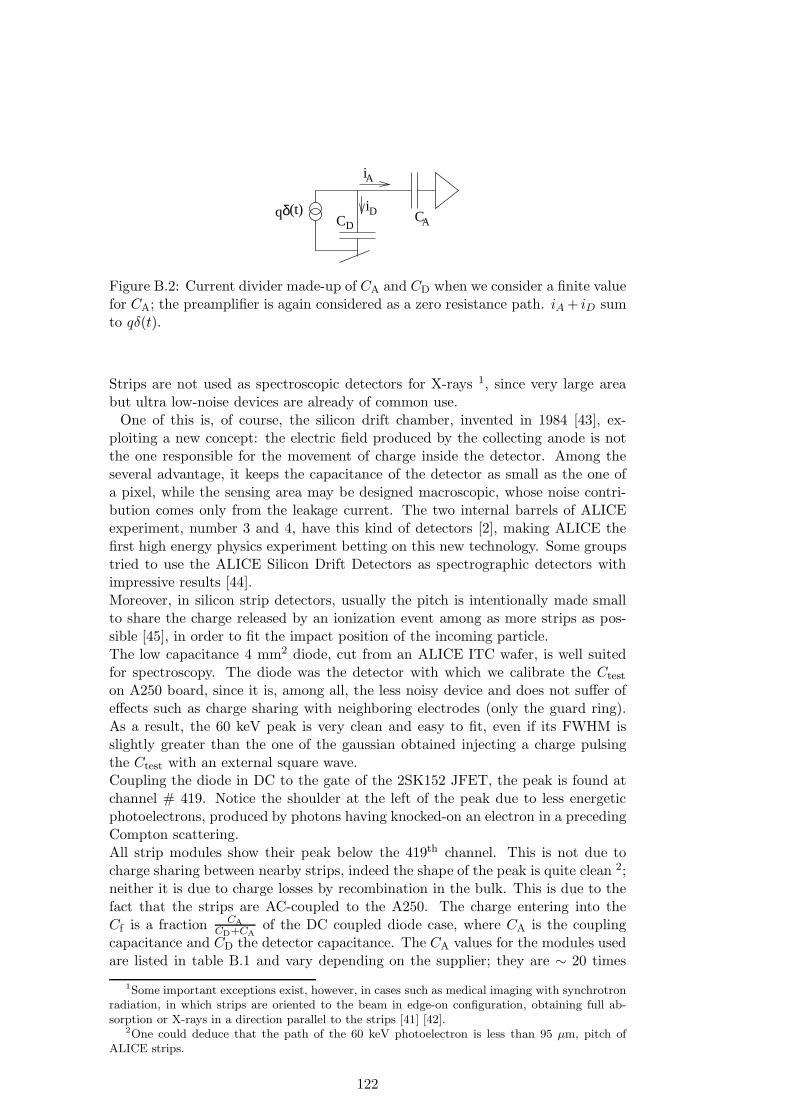
δ(t)qAC
DCDi
Ai
Figure B.2: Current divider made-up of CA and CD when we consider a finite valuefor CA; the preamplifier is again considered as a zero resistance path. iA + iD sumto qδ(t).
Strips are not used as spectroscopic detectors for X-rays 1, since very large areabut ultra low-noise devices are already of common use.
One of this is, of course, the silicon drift chamber, invented in 1984 [43], ex-ploiting a new concept: the electric field produced by the collecting anode is notthe one responsible for the movement of charge inside the detector. Among theseveral advantage, it keeps the capacitance of the detector as small as the one ofa pixel, while the sensing area may be designed macroscopic, whose noise contri-bution comes only from the leakage current. The two internal barrels of ALICEexperiment, number 3 and 4, have this kind of detectors [2], making ALICE thefirst high energy physics experiment betting on this new technology. Some groupstried to use the ALICE Silicon Drift Detectors as spectrographic detectors withimpressive results [44].Moreover, in silicon strip detectors, usually the pitch is intentionally made smallto share the charge released by an ionization event among as more strips as pos-sible [45], in order to fit the impact position of the incoming particle.The low capacitance 4 mm2 diode, cut from an ALICE ITC wafer, is well suitedfor spectroscopy. The diode was the detector with which we calibrate the Ctest
on A250 board, since it is, among all, the less noisy device and does not suffer ofeffects such as charge sharing with neighboring electrodes (only the guard ring).As a result, the 60 keV peak is very clean and easy to fit, even if its FWHM isslightly greater than the one of the gaussian obtained injecting a charge pulsingthe Ctest with an external square wave.Coupling the diode in DC to the gate of the 2SK152 JFET, the peak is found atchannel # 419. Notice the shoulder at the left of the peak due to less energeticphotoelectrons, produced by photons having knocked-on an electron in a precedingCompton scattering.All strip modules show their peak below the 419th channel. This is not due tocharge sharing between nearby strips, indeed the shape of the peak is quite clean 2;neither it is due to charge losses by recombination in the bulk. This is due to thefact that the strips are AC-coupled to the A250. The charge entering into theCf is a fraction CA
CD+CAof the DC coupled diode case, where CA is the coupling
capacitance and CD the detector capacitance. The CA values for the modules usedare listed in table B.1 and vary depending on the supplier; they are ∼ 20 times
1Some important exceptions exist, however, in cases such as medical imaging with synchrotronradiation, in which strips are oriented to the beam in edge-on configuration, obtaining full ab-sorption or X-rays in a direction parallel to the strips [41] [42].
2One could deduce that the path of the 60 keV photoelectron is less than 95 µm, pitch ofALICE strips.
122

CA p-side n-side
CANBERRA 300 290
ITC 320 240
SINTEF 200 180
Table B.1: Measured coupling capacitance CA of the different strip modules. Val-ues in pF. Scan of the AC was one of the measurements aimed to decide the qualityof a detector.
greater than the detector capacitance CD, making the ratio CACA+CD
in the range95% - 97 % and justifying the peak displacement.In chapter 3 we stated that signals and noise generated inside the detector see a“zero” resistance path to the amplifier, so both integrate on Cf .CA, however, is not infinite and must be compared with detector capacitance. Fig-ure B.2 shows how the signal qδ(t) divides itself into two currents by a “currentdivider”: iA, through CA, is equal to qδ(t) CA
CA+CDand iD = qδ(t) CD
CA+CDthrough
the detector capacitance and it does not contribute to the signal. The same holdsfor a fraction CD
CA+CDof the parallel noise, shorted to ground as well as the signal 3.
The assumption that the preamplifier itself is a 0Ω path is taken as true.The low energy shoulder at the left of 60 keV peak can be explained by a minorfraction of events, whose charge is shared between two strips.All these spectra are acquired at the best peaking time for each detector, estimatedby means of noise measurements of the kind of those described in chapter 4. Inthe better detectors, the S/N ratio for a m.i.p should be, with this set-up, greaterthan 100. In our situation, however, we do not have to cope with noise coupledfrom the other channel electronics or with a high rate of signal setting an upperlimit to the peaking time, we can choose the optimum bias voltage and we can usea low-noise single channel amplifier, no matter its power dissipation.Every of these things are not possible in ALICE, which performs however S/N ashigh as 75 [46].
About detector with SF read-out, spectra on PINs are influenced by the lowvalue (3 MΩ) of the bias resistor integrated in the device; being the parallel noise sosignificant, the minimum available peaking time of 0.8µs has been used. The gainis different from the CSA cases and different between them too, so the horizontalscale can be thought of as expressed in arbitrary units. Spectra B.9 is acquiredconnecting the output of the source follower directly to the PX4 shaper, avoidingthe noise contribution from the CSA stage, but being more sensitive to the noiseof PX4 itself.
3since the correction is small, throughout the chapters this consideration has not been takeninto account
123

0 100 200 300 4000
20k
40k
coun
ts
channels
ITC n-side
Figure B.3: Am spectrum acquired with detector AI, n-side, CSA amplifier con-figuration, peaking time 2.4 µs, Vbias = 70 V, ENC = 290 e−, calculated from thestandard deviation of 60 keV peak.
0 100 200 300 4000
20k
40k
60k
coun
ts
channels
ITC p-side
Figure B.4: Am spectrum acquired with detector AI, p-side, CSA amplifier con-figuration, peaking time 4.0 µs, Vbias = 60 V, ENC = 260 e−.
124

0 100 200 300 4000
10k
20k
30k
coun
ts
channels
Canberra n-side
Figure B.5: Am spectrum acquired with detector AE, n-side, CSA amplifier con-figuration, peaking time 0.8 µs, Vbias = 80 V, ENC = 540 e−.
0 100 200 300 4000
25k
50k
75k
coun
ts
channels
Canberra p-side
Figure B.6: Am spectrum acquired with detector AE, p-side, CSA amplifier con-figuration, peaking time 2.4 µs, Vbias = 70 V, ENC = 240 e−.
125
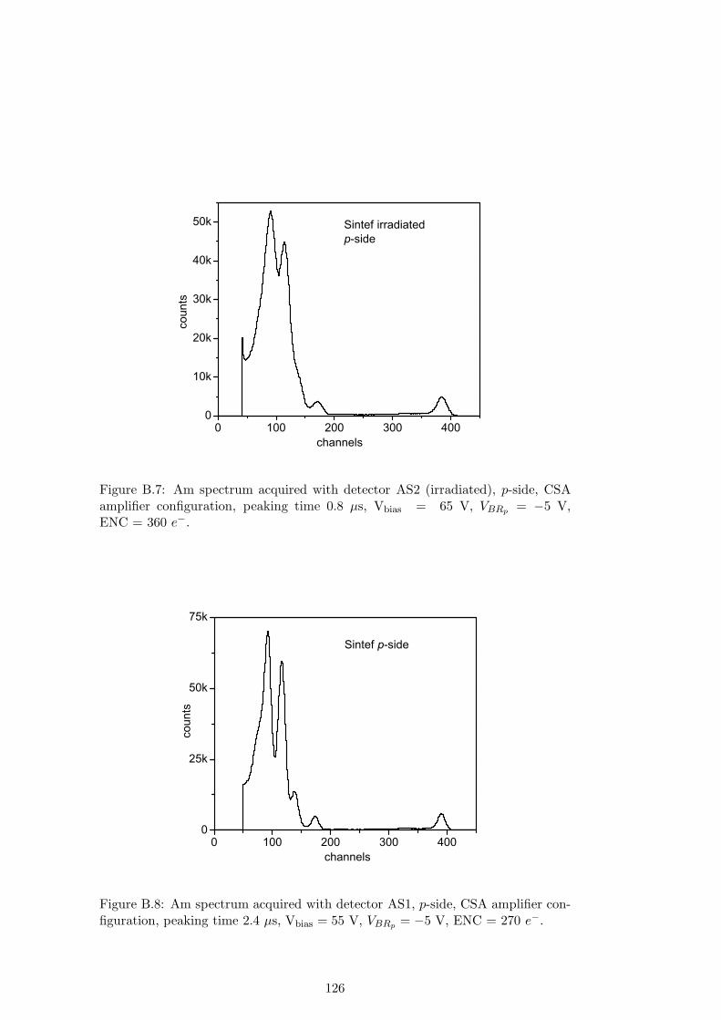
0 100 200 300 4000
10k
20k
30k
40k
50k
co
unts
channels
Sintef irradiatedp-side
Figure B.7: Am spectrum acquired with detector AS2 (irradiated), p-side, CSAamplifier configuration, peaking time 0.8 µs, Vbias = 65 V, VBRp = −5 V,ENC = 360 e−.
0 100 200 300 4000
25k
50k
75k
coun
ts
channels
Sintef p-side
Figure B.8: Am spectrum acquired with detector AS1, p-side, CSA amplifier con-figuration, peaking time 2.4 µs, Vbias = 55 V, VBRp = −5 V, ENC = 270 e−.
126

0 100 200 300 400 5000
10k
20k
30k
40k
coun
ts
channels
PIN1
Figure B.9: Am spectrum acquired with detector PIN1 whose output was di-rectly connected to PX4, without a coupling capacitance, SF configuration, peak-ing time = 0.8 µs, Vbias = 50 V, ENC = 380 e−.
0 100 200 3000
5k
10k
15k
coun
ts
channels
PIN2
Figure B.10: Am spectrum acquired with detector PIN2, CA= 67 pF, SF configu-ration, peaking time = 0.8 µs, Vbias = 50 V, ENC = 330 e−.
127

128

Bibliography
[1] Kemmer J. Fabrication of low noise silicon radiation detectors by the planarprocess. Nucl. Instr. and Meth., 169:499, 1980.
[2] ALICE - technical design report, ITS inner tracking system. CERN/LHCC99-12, ALICE TDR 4, 18 June 1999.
[3] Kuijer P. The Inner Tracking System of the ALICE experiment. Nucl. Instr.
and Meth. A, 530:28, 2004.
[4] Bosisio L. et al. Experience with the test and qualification of double-sidedsilicon microstrip sensors for the ALICE Inner Tracking System. IEEE NSS
Conference Record, page 1429, 2006.
[5] Rashevskaya I. et al. Qualification of a large number of double-sided siliconmicrostrip sensors for the ALICE Inner Tracking System. Nucl. Instr. and
Meth. A, 572:122, 2007.
[6] Holl P. et al. A double-sided silicon strip detector with capacitive read-out anda new method of integrated bias coupling. IEEE Trans. Nucl. Sci., 36:251,1989.
[7] Persky G. Chu J.L. and Sze S.M. Thermionic injection and space-charge-limited-current in reach-through p+ − n − p+ structures. J. Appl. Phys.,43:3510, 1972.
[8] Lutz G. Semiconductor radiation detectors. Springer, 1999.
[9] Rachevskaia I. et al. Test and quality control of double-sided silicon microstripsensors for the ALICE experiment. Nucl. Instr. and Meth. A, 530:59, 2004.
[10] Ghandhi S.K. Semiconductor power devices. Wiley, 1977.
[11] Gatti E. and Manfredi P.F. Processing the signals from solid state detectorsin elementary particle physics. Rivista del Nuovo Cimento, 9, 1986.
[12] Schroder D.K. Semiconductor material and device characterization. Wiley,2nd edition, 1998.
[13] Westgaard T. Schjolberg-Henriksen K. and Sundby-Avset B. HERA-B detec-tors with p-spray isolation on the n-side; unirradiated results. IEEE Trans.
Nucl. Sci., 47:1371, 2000.
[14] Dalla Betta G.-F. et al. Feasibility studies of microelectrode silicon detectorswith integrated electronics. Nucl. Instr. and Meth. A, 478:372, 2002.
129

[15] Dalla Betta G.-F. et al. A fabrication process for silicon microstrip detectorswith integrated front-end electronics. IEEE Trans. Nucl. Sci., 49:1022, 2002.
[16] Dalla Betta G.-F. et al. Silicon pin radiation detectors with on-chip front-endjunction field effect transistors. Nucl. Instr. and Meth. A, 417:325, 1998.
[17] Dalla Betta G.-F. et al. Monolithic integration of Si-PIN diodes and n-channeldouble-gate JFET’s for room temperature X-ray spectroscopy. Nucl. Instr.
and Meth. A, 458:275, 2001.
[18] Piemonte C. Process simulations of a fabrication technology for detectorcompatible front-end circuits on high resistivity silicon. ITC-irst InternalReport, Ref.No. 0306-02, 2003.
[19] Piemonte C. et al. An improved fabrication process for Si-detector-compatibleJFETs. Nucl. Instr. and Meth. A, 568:314, 2006.
[20] ISE-TCAD, ISE Integrated System Engineering AG, Zurich, CH. SoftwareRelease 7.0.
[21] Horowitz P. and Hill W. The Art of Electronics. Cambridge University Press,1989.
[22] Fiorini C. and Lechner P. Charge sensitive preamplifier with continuous resetby means of the gate-to-drain current of the JFET integrated on the detector.IEEE Trans. Nucl. Sci., 49:1147, 2002.
[23] Buckingham M.J. Noise in electronic devices and systems. Ellis HorwoodLtd., 1983.
[24] Johnson J. Thermal agitation of electricity in conductors. Phys. Rev., 32:97,1928.
[25] Nyquist H. Thermal agitation of electric charge in conductors. Phys. Rev.,32:110, 1928.
[26] Spieler H. Semiconductor Detector Systems. Oxford University Press, 2005.
[27] Fitzgerald D.J. Hsu S.T. and Grove A. Surface state related l/f noise in p-njunction and MOS transistor. Appl. Phys. Lett., 12:287, 1968.
[28] Radeka V. Low-noise techniques in detectors. Ann. Rev. Nucl. and Particle
Sci., 38:217, 1988.
[29] Ratti L. private communication.
[30] Manghisoni M. et al. Integrated front-end electronics in a detector compati-ble process. Source-Follower and Charge-Sensitive preamplifier configuration.Proc. SPIE Hard X-rays and Gamma-rays Det. Phys. III, 4507:141, 2001.
[31] Muller R.S. and Kamins T.I. Device Electronics for Integrated Circuits. Wiley,2nd edition, 1986.
[32] Kostner S. and Straussmann U. Noise considerations of the BEETLE amplifierused with long silicon strip detectors. 2005. LHCb note 2005-029.
130

[33] Andricek L. et al. Single sided p+n and double-sided silicon strip detectorexposed to fluences up to 2 1014/cm2 24 gev protons. Nucl. Instr. and Meth.
A, 409:184, 1998.
[34] Azzi P. et al. Radiation damage experience at CDF with SVX. Nucl. Instr.
and Meth. A, 383:155, 1996.
[35] Mathematica 6.0. www.wolfram.com/products/mathematica/index.html.
[36] Dalla Betta G.-F. et al. Monolithic integration of detectors and transistorson high-resistivity silicon. Nucl. Instr. and Meth. A, 579:658, 2007.
[37] www.amptek.com/px4.html.
[38] focus.ti.com/docs/toolsw/folders/print/tina-ti.html.
[39] Fasoli L. Sampietro M. and Bertuccio G. Source Follower or Charge Ampli-fier? an experimental comparison using a detector with integrated electronics.IEEE Trans. Nucl. Sci., 43:2413, 1996.
[40] Hopman P.I. et al. Optimization of silicon microstrip detector design forCLEO III. Nucl. Instr. and Meth. A, 383:98, 1996.
[41] Arfelli F. et al. Design and evaluation of AC-coupled, FOXFET-biased, “edge-on” silicon strip detectors for X-rays imaging. Nucl. Instr. and Meth. A,385:311, 1997.
[42] Vrtacnik C. et al. FOXFET in PIN diode strip detector. IEEE Africon,2:1189, 1999.
[43] Gatti E. and Rehak P. Semiconductor drift chamber - an application of anovel charge transport scheme. Nucl. Instr. and Meth., 225:608, 1984.
[44] Zampa G. et al. Very large area silicon drift detector spectroscopic perfor-mances. IEEE NSS Conference Record, page 3790, 2006.
[45] Belau E. et al. Charge collection in silicon strip detectors. Nucl. Instr. and
Meth., 214:253, 1983.
[46] Sokolov O. Prototyping of Silicon Strip Detectors for the Inner Tracking
System of the ALICE experiment. PhD thesis, Utrecht University, 2006.
131