statusand applicationsof diamond and diamond-likematerials
109
BTIC FILECOPY AD-/_,222 986 STATUSAND APPLICATIONS OF DIAMOND AND DIAMOND-LIKEMATERIALS: %NEMERGINGTECHNOLOGY I q _lkp_vK! tor publi.o relecBe; National Materials Advisory Board C" Commission on Engineering and Technical Systems National ResearchCouncil _. I,_:_... !,.._ .., ,I! I..., _
-
Upload
khangminh22 -
Category
Documents
-
view
3 -
download
0
Transcript of statusand applicationsof diamond and diamond-likematerials
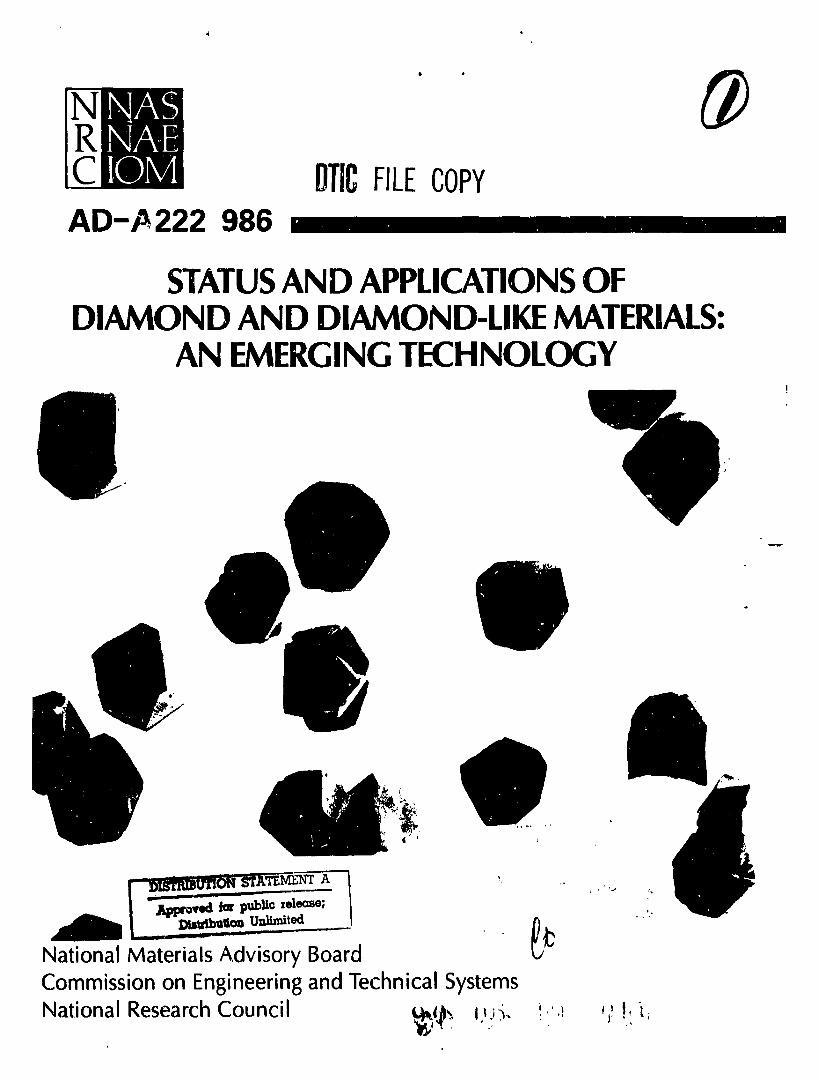
BTICFILECOPYAD-/_,222 986
STATUSAND APPLICATIONSOFDIAMOND AND DIAMOND-LIKEMATERIALS:
%NEMERGINGTECHNOLOGYI
q
_lkp_vK! tor publi.orelecBe;
National Materials Advisory Board C"Commission on Engineeringand Technical Systems
National ResearchCouncil _. I,_:_... !,.._.., ,I! I...,_
1990017647
NATIONAL RESEARCH COUNCIL
COMMISSION ON ENGINEERING AN[) TECHNICAl. SYSTEMS
NATIONAL MATERIALS ADVISORY BOARD
The purpose of the National Materials Advisory Board
is the advancement of materials science and engineering in the national interest.
CHAIRMAN PAST CHAIRMAN
Dr. James C. Williams Dr. Bem_d H. KearGeneral Manager Chairman. Department ofMaterials Technology Laboratories Mechanics andMaterials ScienceMail Drop #85 Director, Center for MaterialsGeneral Electric Company SynthesisI Neumann Way College of EngineeringCincinnati, OH 45215-6301 Rutgers University
P.O. Box 909Piscataw,sy. NJ 08854
MEMBERS
Dr. Norberl S. Baer Dr. Frank E. Jamerson Dr. John P. giggsHagop Kevorkian Professor of Manager _'ice President, R&D Research
Conservation Division and Staff Cont,lcts DivisionNew York University General Motors Resea-ch Managing Director. MitchellConservation Center of the Institute Laboratories Technical Center
of Fine Arts 30500 Mound Road Hoechst Celanese Corporation14East 78th Street Warren. MI 48090-9055 86 Morns AvenueNew York, NY 10021 Summit, NJ 07901
Dr. Melvin F. KanninenMr. Robert R. Beebe Institute Scientist Dr. Maxine L. SavitzSenior Vice President Southwest Resear 'h Institute DirectorHomestake MiningCompany P.O. Drawer 285_ , Garrett Ceramic Components650 California Street San Antonio. TX 78284 DivisionSan Francisco. CA 94108 Allied-Signal Aerospace Co.
Dr. gonald M. Latanision 19800South Van Ness AvenueDr. Frank W. Crossman Professor of Materials Science & Torrance, CA 90509Assistant Director Engineering. and Director,Telecommunications, Systems & Operat,ons Materials Processing Center Dr. Dale F. SteinLockheed Missiles & Space Co,, Inc. Room 8-202 PresidentOrg. No. 19-60, Bldg. 102 Massachusetts Institute of Michigan Technological UniversityP.O. Box 3504 Technology Houghton. MI 49931Sunnyvale. CA 94088-3, 04 Cambridge. MA 02139
Dr. Earl R. ThompsonDr. James Economy Dr. Robert A. Laudise Assistant Director of Research forProfessor & Head of Materials Director, Physical and Inorganic Materials Technology
Science Chemistry Research Laboratory United Technologies ResearchUniversity of Illinois Room IA-264 CenterDepartment of Material_Science & AT&T Bell Laboratories Silver Lane
Engineering Murray Hill, NJ 07974 East Hartford, CT 061081304Green StreetUrbana, IL 61801 De. William D. Nix Mr. James R. Weir, Jr.
Professor, Department of Materials Associate DirectorDr. James A. Ford Science and Engineering Metals & Ceramics DivisionConsultant Stanford University Oak Ridge National Laboratory703Judith Drive Stanford. CA 94305 P.O. Box X
Oak Ridge, TN 37830Johnson City. TN 37604 Dr. Donald R. Paul
Melvin H. Gertz Regents Chair Dr. Robert M. WhiteDr. Robert E. Green, Jr. in Chemical Engineenng Vice PresidentDirector of Center for NDE Director, Center for Polymer MCCProfessor. Materials Science Research 3500 West Balcones Center Drive
Department Department of Chemical Austin, TX 78759Johns Hopkins University EngineeringBaltimore, MD 21218 University of Texas
Austin, TX 78712 NMAB STAFFDr. John K, HulmChief Scientist Emeritus Dr. Joseph L. Pentecost K,M. gwdsky, DirectorWestinghouse Research Professor S.M. Barkin, Assoc. Director
Laboratories School of Materials Engineering Mary Brittain, Adm. Officer1310Beulah Road Georgia Institute of Technology 2101 Constitution Ave., NWPittsburgh, PA 15235 Atlanta. Ga 30332 Washirgton, DC 20418 3/90
1990017647-002

UNCLASSIFIED
SECURITYCLASSIFICATIONOF THISPAGE
REPORTDOCUMENTATIONPAGEIII II
1'1.REVvlRTSECURITYCLASSIFICATION lb. RESTRICTIVEMARKINGS
UNCI_ASSIFIED NONE21. SECURITYCLASSIFICATI()NAUT_-OI_ITY 3. DISTRIBUTION/AVAILABILITYC_:REPORT
N/A Approved for Public ReleaseIIII
2b.bECLASSIF_:ATK)NIDOWNGP_t_)INGSCHEDULE Distribution UnlimitedN/A
I
4. _ERFORMINGOR(JANiZATIONREPORTNUMBER(S) S. MONITORINGORGANIZATIONREPORTNUMBER(S)
NMAB-445
Cm.NAME OFPERFORMINGORGANIZATION_ " 6b OFFIC$$YMilOL 71. NAMEOF MONITORINGORGANIZATION
National Materials Advisor_ @fN_/_mJ_e) Department of Defense/National Aeronautics
Board NMAB and Space Administration
6(. ADDRESS(Or).,S_ate.o_d ZlPCode) 7b &DDRESS(CRy,SM_e.br_ ZheCode)2101 Constitution Avenue
Washington, DC 20418 Washington, DC 20301
Ikl.NAMEOF FU'I_DING'/SPONSORING 8b OFFICESYMBOL 9.PROCUREMENTINSTRUMENTIDENTIFICATIONNUMBERORGANIZATION Of _b_)see 7a MDA 903-89-K-0078
II III
_. ADDRESS(CRy,State,or_ ZIPCode) 10 SOURCEOF FUNDII_IGWIJMBERSPROGRAM PROJECT TASK WORKUNITELEMENTNO. NO NO. ACCESSIONNO.
Washington, DC 20301
11.TITLE(/nc/_le SecurRyI_f_)"
Status and Application of Diamond and Diamond-Like Material s: An Emerging Technology
12.PERSONALAUTHOR(S)
I I im ii
13a. TYPEOFREPORTOne of a 13b.TIMECOVERED 114.DATEOF REPORT(Year,Month, DRy) JIB. 6_3% COUNT
series un_r contract FROM 1987 TO 1990 J 1990 April 30 I 115{ J .%' El
- .sI I i I i I __
17 COSATICODES ..... , IUIJ| ERMS(Cont/nueneteBv_tlw/f necemry snd ide b/ock numb_r)._
\, " FIELD GROUP SUI_ROU, "6_amond] diamond-like hydrocarbons\carlM)n.s_ chem£cai .& vapor, "" deposltton processes; ion Implantation; cnara;terizatton
_. techniques'; thermal conducttvity_, applicatons; PAD issues,/
,9:_sT_ (c.,,.. o.._,. _ _ _ _ _ _ _,) '-_cent discoveries that make possible the growth of crystalline diamond by
cnemlcal vapor deposition offer the potential for a wide variety of new
applications. This report takes a broad look at the state of the technology
following from these discoveries in relation to other allied materials, such as
hlgh-pressure diamond and cubic boron nltrlde. Most o£ the po_entla! defense,
space, and commercial applications are related to diamond's hardness, but some
utilize other aspects such as optical or electronic properties. The growth
processes are reviewed, and techniques for characterizin8 the resultingmaterials' properties are discussed. Crystalline diamond is emphastzed: _but
other dia=ond-llke materials (silicon carbide, amorphous carbon containinghydrogen) are also examined. Scientific, technical, and economic problem area sthat could impede the rapid exploitation of these materials are identified.',
Recommendations are p_'esented covering broad areas of research and development_I IIII I
20. DISTRIBUTION/AVAiLABiLITYOF ABSTRACT 21. ABSTRACTSE'_RITYCLASSIFICATIONr_UNCLA.SSIFIEINUNLIMIT[D I"1 SAMEAS RPT. _] DTI¢ USERS UNCLASSIFIED
"2_1. NAMEOF P_SPONSIIILEINDIVIDUAL 2-_b.TELEP;40NE(M_ludeAnsi Code)i _2c.OFFICESYMBOLJerome Persh (202) 695-,0005 OUSDR&E/ReAT/MST
lU I
DD FORM 147|. 14MAR LI APR_mon rely beulecl unt,lelheuS_K:. _ SECURITYCLAS}IFIC,_kTIONOFTHt} PAGE_li c_her,:cl_ns ire olxo_e.
1990017647-003

STATUSAND APPLICATIONSOFDIAMOND AND DIAMOND-LIKEMATERIALS:
AN EMERGINGTECHNOIOGY
I i
Accession For
gHTIS GRA&I
DTIC TAB @
Unannounced []Justi_Icatlon
By
Distribution/
Availability Codes
iAvall and/or
Dlst I Special
1990017647-004

1990017647-005

STATUSAND APPLICATIONSOFDIAMOND AND DIAMOND-LIKEMATERIALS:
AN EMERGINGTECHNOLOGY
Report of the Committee on Superhard Materials
NATIONAL MATERIALS ADVISORY BOARDCommission on Engineering and Technical Systems
National Research Council
NMAB-445National Academy Press
1990
1990017647-006
NOTICE: The project that h the subject of this report was appro%,ed by the Governing Board ofthe National Research Council, whose members are drawn from the councils of the NationalAcademy of Sciences, the National Academy of Engineering, and the Institute of Medicine. Themembers of the committee responsible for the report were chosen for their special competences andwith regard for appropriate balance.
This report has been reviewed by a group other than the authors according to procedures_pproved by a Report Review Committee consisting of members of the National Academy ofSciences, the National Academy of Engineering, and the Institute of Medicine.
The National Academy of Sciences is a private, nonprofit, self-perpetuating society ofdistinguished scholars engaged in scientific and engineering research, dedicated to the furtheranceof science and technology and to their use for the general welfare. Upon the authority of the chartergranted to it by the Congress in 1863, the Academy has a mandate that requires it to advise thefederal government on scientific and technical matters. Dr. Frank Press is presldent of the NationalAcademy of Sciences.
The National Academy of Engineering was established in 1964, under the charter of theNational Academy of Sciences, as a parallel organization of outstanding engineers. It is autonomousin its administration and in the selection of its members, sharing with the National Academy ofSciences the responsiblity for advising the federal gcvernment. Tile National Academy ofEngineering also sponsors engineering programs aimed at meeting national needs, encourageseducation and research, and recognizes the superior achievements of engineers. Dr. Robert M. Whiteis president of the Nationnl Academy of Engineering.
The Institute of Medicine was established in 1970 by the National Academy of Science_ tosecure the services of eminent members of appropriate professions in the examination of policymatters pertaining to the health of the public. The Institute acts under the responsibility given tothe National Academy of Sciences by its congressiona! charter to be an adviser to the federalgovernment and, upon it_own initiative, to identify issues of medical care, research, and education.Dr. Samuel O. Thief is president of the Institute of Medicine.
The National Research Council was organized by the National Academy of Sciences in 1916to associate the broad community of science and technology with the Academy's purpo_s offurthering knowledge and advising the federal government. Functioning in accordance with generalpolicies determined by the Academy, the Council has become the principal operating agency of boththe National Academy of Sciences and the National Academy of Engineering in providing servicesto the government, the public, and the scientific and engineering cowraunities. The Council isadministered jointly by both Academies and the Institute of Medicine. D._. Frank Pre_s mid Dr.Robert M. White are chairman and vice chairman, respectively, of the National Research Council.
This study by the National Materials Advisory Board was conducted under Contract No.MDA-903-89-K-0078 with the Department of Defense and the National Aeronautics and SpaceAdministration.
Library of Congress Card Number 90-60384.International Standard Book Number 0-309-04196- i.
This report is available from the Defense Technical Information Center, Cameron Station,Alexandria, VA 22304-6148.
SIO0.
Corr." Small single crystal diamonds oroduced by AFCI filament assisted CVD process(Courtesy of Air Products and Chemicals. Inc.)
Frontispiece:ContinuouspolycrystallinediamondcoalingproducedbyAPCI filamentassisted CVD Trocess (Courtesy of Air Products and Chemicals, Inc.)
Printed in _he Ueited States of America.
1990017647-007
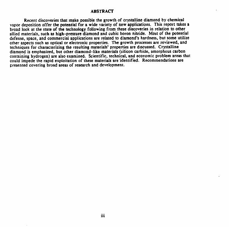
ABSTRACT
Recent discoveries that make possible the growth of crystalline diamond by chemicalvapor deposition offer the potential for a wide variety of new applications. This report takes abroad look at the state of the technology following from these discoveries in relation to otherallied materials, such as high-pressure diamond and cubic boron nitride. Most of the potentialdefense, space, and commercial applications are related to diamond's hardness, but some utilizeother aspects such as optical or electronic properties. The growth processes are reviewed, andtechniques for characterizing the resulting materials' properties are dmcussed. Crystallinediamond is emphasized, but other diamond-like materials (silicon carbide, amorphous carboncontaining hydrogen) are also examined. Scientific, technical, and economic problem areas thatcould impede the rapid exploitation of these materials are 'identified. Recommendations arepresented covering broad areas of research and development.
ooo
111
1990017647-008

ACKNOWLEDGMENTS
Valuable briefings were presented to the committee by Professor Robert Davis, NorthCarolina State University, who discussed epitaxy, doping, and characterization of nanocrystalline
SiC thin films, and Dr. Jobn W. Coburn, IBM, who spoke on mechanistic aspects of diamondfilm deposition. The committee, acknowledges their assistance with thanks.
1990017647-009

COMMITTEE ON SUPERHARD MATERIALS
CHAIRMAN
JOHN Do VENABLES, Corporate Scientist, Martin Marietta Laboratories, Baltimore, Maryland
VICE CHAIRMAN.
JACK H. WERNICK, Manager, Division of Materials Science, Bell Commuaications Research,Inc., Red Bank, New Jersey
MEMBERS
JOHN C. ANGUS, Professor of Engineering, Chemical Engineering Department, Case WesternReserve University, Cleveland, Ohio
PETER M. BELL, Vice President, Corporate Technology, Norton Company, Worcester,Massachusetts
JEROME J. CUOMO, Manager, CCS Materials Laboratory, IBM, Thomas J. Watson ResearchCenter, Yorktown Heights, New York
ROBERT C. DEVRIES, General Electric Company (Retired), Burnt Hills, New York
ALBERT FELDMAN, Leader, Optical Materials Group, National Institute of Standards andTechnology, Gaithersburg, Maryland
MICHAEL W. GELS, Staff Member, M.I.T. Lincoln Laboratories, Lexington, Massachusetts
DAVID S. HOOVER, Manager, Inorganic Materials, Air Products and Chemicals, Inc.,Allentown, Pennsylvania
RUSSELL MESSIER, Associate Professor, Engineering Science and Mechanics, PennsylvaniaState University, University Park
LIAISON REPRESENTATIVES
JEROME PERSH, Department of Defense (OUSDR&E), Washington, D.C.
T. W. ItASS, Air Force Wright Aeronautical Laboratories, Wright-Pattersoa Air Force Base, Ohio
vii
1990017647-010

ROBERT KATZ. Army Materials Technology Laboratory, Watertown. M_ssachusctts
MAX N. YODER, Office of Naval Research, Arlington, Virginia
ROBER'I" POHANKA, Office of Naval Research, Arlington: Virginia
BEN A. WILCOX, Defense Advanced Research Projects Agency, Arlington, Virginia
ROBERT i USARO, NASA Lewis Research Center, Cleveland, Ohio
NMAB STAFF
,JOSEPH R. LANE, Senior Program OfficerJUDITH A. AMRI, Senior SecretaryCATItRYN SUMMERS, Senior Secretary
.°,VIII
1990017647-011
CONTENTS
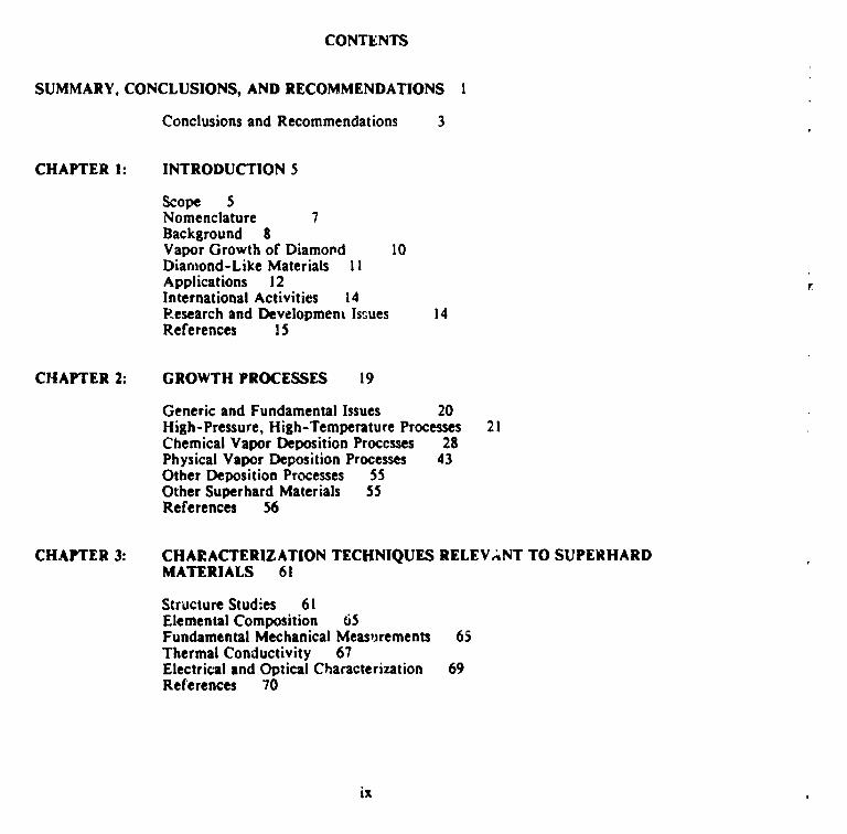
SUMMARY, CONCLUSIONS, AND RECOMMENDATIONS I
Conclusions and Recommendations 3
CHAPTER I: INTRODUCTION 5
Scope 5Nomenclature 7Background 8Vapor Growth of Diamond I0Diamond-Like Materials IIApplications 12 rInternational Activities 14P,esearch and Developmem Issues 14References 15
CHAPTER 2: GROWTH PROCESSES 19
Generic and Fundamental Issues 20High-Pressure, High-Temperature Processes 21Chemical Vapor Deposition Processes 28Physical Vapor Deposition Processes 43Other Deposition Processes 55Other Superhard Materials 55References 56
CHAPTER 3: CHARACTERIZATION TECHNIQUES RELEV,_NT TO SUPERHARDMATERIALS 61
Structure Studies 61Elemental Composition 65FundamentalMechanicalMeas,jrements 65Thermal Conductivity 67Electrical and Optical Characterization 69References 70
iX
1990017647-012
CHAPTER 4: APPLICATIONS 73
Mechanical Applications 75Electronics 78Optics and Optoelectronics 83References 88
CHAPTER 5: RESEARCH ANI_ DEVELOPMENT ISSUES AND OPPORTUNITIES 91
Growth Processes 92Materials CI"..racterization 93Applications 93Beyond Diamond: Other Materials and Issues 94References 95
APPENDIX: BIOGRAPHICAL SKETCHES OF COMMITTEE MEMBERS 97
X
1990017647-013
TABLES AND FIGURES
Table 1=i Nomenclature for Diamond=Like Materials 7
Table 1-2 Some Properties of Natural Type IIA Diamond and Vapor-Grown Diamond 12
Table 2-1 Plasma-Enhanced Chemical Vapor Deposition (PECVD) Processesfor Diamond Film Growth 30
Table 2-2 Nonplasma Deposition Processes for Diamond Film Growth 33
Table 2-3 Deposition Data for DLC, BN, and Related Composites 45-46
Table 4-1 Mechanical and Thermal Applications of Superhard Materials 73
Table 4-2 Potential Electronic Applications of Superhard Materials 74
Table 4-3 Optical and Optoelectronic Applications of Superhard Materials "/5
Table 4-4 Relative Figures of Merit for Electronics 78
Table 4-5 Figures of Merit for Thermal Stress Resistance 84
Figure 1- 1 Number of papers published in scientific journals on low-pressure growthof diamond and diamond-like materials 6
Figure 1-2 Hard materials in the composition tetrahedron C-B-N-Si 6
Figure 1-3 Microhardness versus atomic number density 8
Figure 1-4 Equilibrium phase diagram for the carbon system 9
Figure 2-1 The Hall "belt"apparatus 23
Figure 2-2 Cell design for growth of large crystals of diamond or cubic BN usinga temperature gradient between carbon source and the seed crystal 25
Figure 2-3 Morphology of diamond from metal solutions as a function of pressureand temperature 26
xi
1990017647-014

Figure 2=4 Schematicrepresentationof the four principal types of diamondin termsof the systems B-C and C-N 27
Figure 2-5 Schematicdiagramsof variousplasma-enhancedCVD techniquesfordiamond growth 31
Figure 2-6 Statisticsof abstracts published at the meetings of the JapaneseAppliedPhysics Society on different preparationmethodsfor diamond thin films
32
Figure 2-7 Schematicdiagramsof two different nonplasmaapproachesfor diamondgrowth 33
Figure 2-8 Ratioof diamond to graphite nucleationvelocity as a functionof supersaturation 37
Figure 2-9 Relative growth and etch rates of diamond and graphite in the presenceof a hydrocarbon(CH4)and atomic hydrogen 38
Figure 2-10 CH4(open squares)and CzHz(solid circles) mole fractions at thegrowing diamond surface as a function of distance between substrateandfilament 39
Figure 2-11 Processesfor growing carbon films from hydrocarbongases 44
Figure 2-12 Processesfor growing carbon films using solid carbon 44
Figure 2-13 Ion plating configuration 49
Figure 2-14 RF plasmaconfiguration 50
Figure 2-15 Direct ion beamclepositionfrom solid precursoronfiguration 50
Figure 2-16 Direct ion beam deposition from gaseous precursorconfiguration 51
Figure 2-17 Dual ion beam deposition configuration 52
Figure 2-18 Ion beam sputteringwith ion beam assist configuration 52
Figure 3-1 Raman spectra of diamond, graphite.,and microcrystallinegraphite 62
Figure 3-2 Atom numberdensity versus atom fraction hydrogen 66
Figure 3-3 The thermalconductivity of variousmaterials as a functionof temperature 67
xii
1990017647-015
SUMMARY, CONCLUSIONS, AND RECOMMENDATIONS
Recent success in deposition of diamond and diamond-like coatings on a variety ofsubstrates at practical growth rates is one of the most important technological developments in thepast decade. It places within the reach of s_:ience and industry an opportunity to exploit themany desirz.ble extreme properties of these materials (e.g., modulus, hardness, thermalconduc+.ivity, high breakdown voltage). Indeed, the ultimate economic in,pact of thi_ technologymay well outstrip that of high-temperature superconductors. Consequently, it is imperative thatthe United States take a leading role in the commercialization of diamond technology.
The committee focused on materials that can be grown at practical growth rates byvarious vapor-phase techniques. These include principally diamond, diamond-like hydrocarbons(DLHC), and diamond-like carbons (DLC).
, Diamond--This refers to crystalline diamond grown at relatively low pressure byvarious chemical vapor-deposition (CVD) processes in the presence of hydrogen andhydrocarbons such as methane. Substrate temperatures generally are required to be above 600"C.Surface morphology is usually faceted.
. Diamond-like hydrocarbons (DLHC)--These are metastable, amorphous materialsprepared by various techniques (e.g., ion beam deposition) involving thermal decomposition ofhydrocarbons and having atomic number densities greater than approximately 0.19 g-atom/era 3.Hydrogen content ranges from 17 atomic percent to 60 atomic percent. Properties vary widely,depending on hydrogen content; surface finish is usually optically smooth, and substratetemperature requirement is low (<150"C).
• Diamond-like carbons (DLC)--There is evidence to suggest that hydrogen-free DLCfilms exist. These might be considered "microcrystailine" diamond, but much work remains tofurther describe their structure and properties.
• Other materials--In addition to the foregoing, the study includes a discussion of high-pressure diamond to provide background for the low-pressure processes and to indicatetechnological opportunities for the mote conventional approach to diamond manufacturing. Also,a brief description of related materials involving boron, carbon, nitrogen, and silicon is given,with particular emphasis on SiC and BN.
The ability to deposit diamond and diamond-like films on a variety of substrates(including diamond-like materials on paper and plastics) vastly expands the potential applicationareas for these materials over that possible with high-pressure, high-temperature technology.
1990017647-016
2
Althou_hcurrentapplicationsinactualproductionarelimitedtohigh-modulustweeterspeakercones(forimprovedhigh=frequencyperformance)and instrumentwin_.',:s,otherusesarebeingactivelypursued.The committeefeltthatthereareapplicationsthathavenotbeenrealizedbutwhichexhibitpotentialforhighpayoff,assumingadequatefunding.
Inelectronics,thereispotentialpayoffinthefollowingapplicatioas:
• High=temperatureelectronicsforspacewithimprovedheatdissipationcapabilityviatheT4dependencefortheradiationofenergy.
• Coldcathodes(currentdensitiesgreaterthan1000A/cm z)thattakeadvantageofexpectedlow work function.
• Thermalconductorsand heatsinks,particularlyforelectronicpackages.
• High-power,high=efficiencyradarelectronics,witha potentialfora hundredfoldincreaseinpower capabilityoversilicontransistors.
• Solar=blinddetectors,whichtakeadvantageofthelargeenergygap(greaterthan6.4eV) of BN.
Inoptics,potentialpayoffscouldoccurinthefollowing:
• Anti=abrasion,anti=erosioncoatingsforinfraredlensesandwindows. Some successhasalreadybeenachieved,forexample,inapplyingdiamond=likecoatingstoZnS and ZnSewindowsusinga Ge-C intermediatelayer.
• Anti-abrasioncoatingson opticalfibersforfiber=optic=guided(FOG) missiles.
• Compact ultravioletlasers(fordiamond,thisrequiresa stress-inducedconversiontoadirect-gapmaterial,possiblyby a strainedsuperlatticeapproach).
• Largesingle-crystalopticalelementsforuseininfrareddevices(e.g.,windows andlenses).
Other potential app!ications could include the following:
• Abrasion-resistant coatings for computer disks and read-write heads.
• Machine tool guides to produce precise, very reproducible parts.
• X=ray lithographic masks.
• Anti=friction (low-friction) coatings for prosthetics.
• Corrosion protection and passivating films.
As more and more potential applications of diamond and diamond-like films becameappsrent, it was clear that the impact of this emerging technology on the defense, space, andcommercial sectors could _ival that of high-temperature superconductors but with moreimmediate applications. For this to happen, however, certain technical and economic problemareas must be identified and decisive addressed. Also, some approaches and policies that havebeen carried out correctly in the past should be encouraged and promoted. Few applications have
1990017647-017
as yet reached the marketplace; the enthusiasm of workers in the field is based substantially onthe feelings that applications--often completely unforeseen--follow when a product with uniqueproperties is developed.
CONCLUSIONS AND RECOMMENDATIONS
This emerging technology must be exploited. The following conclusions andrecommendations address those areas that the committee feel will expedite this exploitation.
While General Electric and DeBeer have the bulk of the high-pressure diamond market,Japan apparently leads in vapor-deposited diamond research and development. However, theability to transfer a technological development from the laboratory stage into useful applicationscan be the most difficult part in the growth of a new technology. Fortunately, in the case ofdiamond and diamond-like films, it appears that transfer has been facilitrted by the excellentuniversity, industry, and government interactions that have developed in this country. As aresulq many companies, large and small, are now growing films in the United States afterreceiving training from government- and industry-sponsored programs.
Regvmmendation
Funding for university, industr.,,, and government programs that will turn this emergingtechnology into a national pivotal technology with important useful applications must becontinued and expanded in the future. The programs should be interdisciplinary, withtheoreticians working with chemists, optical scientists, electrical engineers, and materialsscientists to establish relationships among growth processes, structure, and properties. Theyshould be carefully coordinated with and should draw upon the results of the individual basicresearch programs discussed in Conclusion and Recommendation 2. In order to ensure thegreatest impact, emphasis should be placed on the optimization and use of combinations ofproperties (e.g., hardness and infrared transparency for window coatings) for well-definedapplications.
Cotlclusion 2
The new films can exhibit many of the extreme properties that make diamond attractivebut the effect of variables such as hydrogen content, other impurities (dopants), crystallinity, andsp3/sp 2 ratio on mechanical, electrical, and optical properties is not well understood. Anappreciation of the influence of additional elements in the diamond lattice on, for example,tribology could be of considerable industrial significance. Thus, the ability to produce films withpredictable material properties to satisfy specific application requirements is currently lacking.
Reeommendatio_
A coordinated interagency effort i_ recommended to address fundamental problems thathave arisen in attempts to exploit diamond and diamond-like technology applications. Among themost pressing problems that should be addressed are:
• Nucleation and growth processes, with specific emphasis on increasing growth rates ofboth diamcnd and diamond-like films and on growing larger high-quality single crystals ofdiamond for electronic and optical applications. An integral part of this study shuuld besubstrate development and adhesion to substrates. Current work involves deposition from vapor;
1990017647-018
v I
4
other possibilities should be explored. Much needs to be done to enable deposition over largeareas and at lower temperatures.
® Growth of cubic BN films and crystals, with specific emphasis on their use forultraviolet detectors (BN can be doped both p and n type) and solar-blind detectors.
• Modulated structures incorporating layers of BN and diamond, for example, to developmaterials that are harder and/or tougher than diamond.
• Cold cathode development for high-power electron sources (greater than 1000 A/cruz).The basic question to be resolved relates to determining the degree of (negative) electron affinityof the film materials.
• Development of a predictive capability for the stability of various boron, nitrogen, andcarbon alloys and "superdense" carbons through the use of fundamental structure calculations.One question that should be answered: "Is there anything beyond diamond with useful extremeproperties?"
(_0nclusion 3
• Attaining successful electronic devices requires successful coatrolled doping ofdiamond both by CVD and by ion implantation.
Recommendztion
Basic understanding should be developed, through theoretical studies, of doping anddefect formation and their influence on the band structure. Development and understanding ofprocesses for both p-type and n-type doping should also be pursued.
Conclusion 4
The rapid growth of this emerging technology coupled with the wide variety of materialsit can produce (e.g., crystalline and amorphous materials containing large or small amounts ofhydrogen) has led to several different nomenclature schemes, with some resulting confusion.
Recomm_._JKt_.D
The committee recommends that a uniform system of nomenclature be used based on thefollowing principles:
I. ]_iamond films - true crystalline diamond films as produced by a variety of CVDtechniques.
2. Diamond-like films f._} are of two types:
• Diamond-like hydrocarbons (DLHC) - amorphous films grown by a variety of ion-assisted deposition processes and the decomposition of hydrocarbon gases. These films generallycontain between 15 percent and 60 percent hydrogen and have atomic number densities greotrthan 0.19 g-atom/era 3.
• Diamondqike carbons (DLC) - amorphous hydrogen-free carbon films h_vingatomic number densities greater than 0.19 g-atom/cm °.
1990017647-019

1
INTRODUCTION
This study is motivated, in large measure, by recent discoveries that have permitted thegrowth of crystalline diamond by chemical vapor deposition at practical growth rates. Chemicalvapor deposition of diamond has enormous technological potential in areas as diverse as_.lectronics, optics, biomedical implants, abrasives, cutting tools, bearing surfaces, and heat sinks.The related diamond-like materials show great potential for tribological surfaces, corrosionprotection, passivating layers, and diffusion barriers as well as in photolithography.
By way of background, annual world production of natural rough diamonds is about 94million carats (18.7 tons). Synthetic production in weight terms is much larger, possibly 66 tons.Imports of industrial-quality artificial diamonds amount to about 51 million carats (I0 tons). Saleprice is slightly over $1/carat.
Vapor-grown diamond and diamond-like materials may play an important role in a widerange of industries. Their ultimate economic impact may well outstrip that oi high-temperaturesuperconductors. However, despite this promise, there are relatively few applications currentlybeing realized.
Many of the most exciting applications of both diamond and the diamond-like materialsarise from their extreme properties, or combinations of properties, with hardness sometimesunimportant or of secondary importance.
SCOPE
This report reviews the present status of vapor-grown diamond, the diamond-likematerials, and related solids such as SiC and cubic BN. Currer,t developments are considered in abroad context, and directions for future work are recommended.
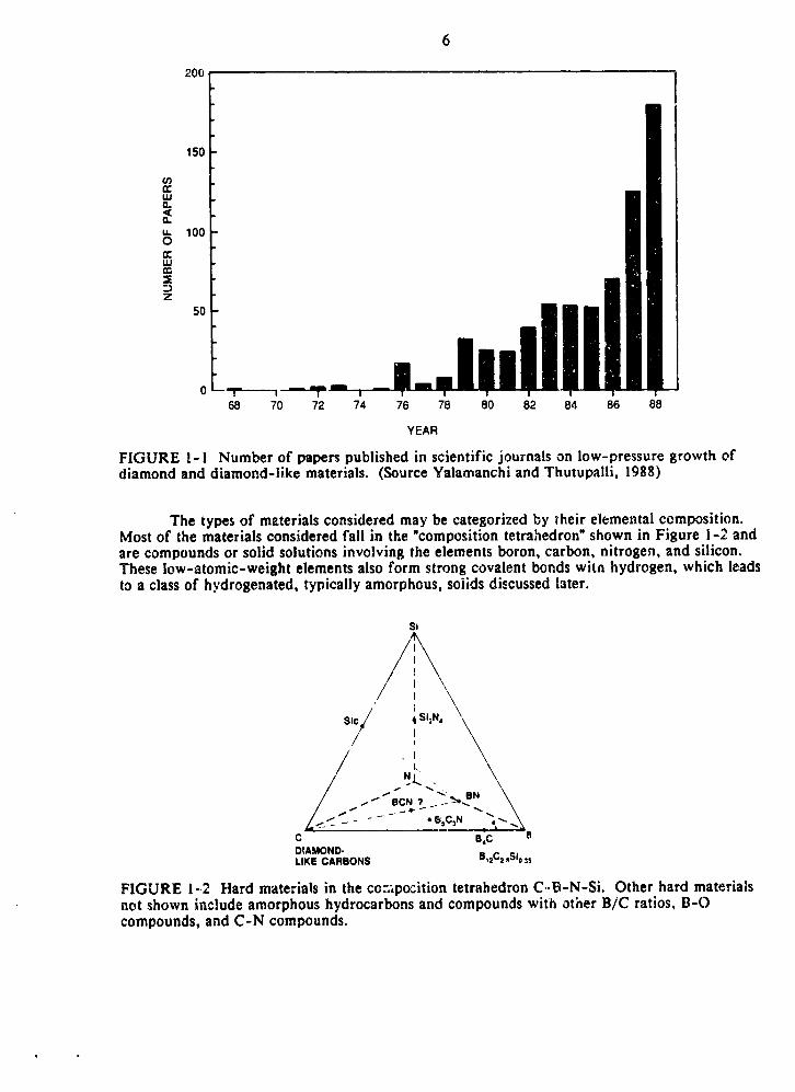
The field of superhard materials is rapidly evolving and has diffuse and expandingboundaries. It is not an exaggeration to say that there has been an explosion of interest in thesubject. Figure 1-I shows the trend in numbers of scientific papers published in the past 20years. The curve is sharply upward, with no indication of peaking.
At the risk of incompleteness, it was necessary to make some arbitrary judgments abouttopics to include. This inevitably reflects the experiences of the members of the committee andshould not necessarily be regarded as a value judgment about the relative importance of topics.
1990017647-020
6
200 !
150
o_0cuJa.
u. 1000n.LU
Z50
068 70 72 74 76 78 80 82 84 86 88
YEAR
FIGURE l-1 Number of paperspublishedin scientific journals on low-pressuregrowth ofdiamondand diamond-like materials. (SourceYalamanchiand Thutupalli, 1988)
The types of m¢terialsconsideredmay be categorizedby their elemental composition.Most of the materialsconsideredfall in the "compositiontetrahedron"shown in Figure 1-2 andare compoundsor solid solutionsinvolving the elementsboron, carbon, nitrogen, and silicon.Theselow-atomic-weight elementsalsoform strongcovalentbondswith hydrogen, which leadsto a classof hydrogenated,typically amorphous,soiidsdiscussedlater.
Si
--:, \,f
• I \
C B_C BDIAMOND-LIKE CARBONS BlaC=mSl03s
FIGURE 1-2 Hard materials in the co.-:,po:itiontetrahedronC..B-N-SI. Other hard materialsnot shown include amorphoushydrocarbonsand compoundswith other B/C ratios, B-Ocompounds,and C-N compounds.
1990017647-021

7
The major emphasis is on crystalline diamond and the so-called diamond-like materials.For the latter the categorization method proposed by Angus and Hayman (1988) is used; coverageis restricted to carbons and hydrocarbons with atomic number densities greater thanapproximately 0.19 g-atom/cm 3. The amorphous diamond-like materials have higher numberdensities than other carbonaceous materials and have a significant fraction of sp3-bonded carbonsites.
Cubic BN ,:rid both hexagonal and cubic SiC are considered because they are structurallyrelated to diamond and have overlapping areas of application. Other recently reported hardmaterials in the C-N and B-O systems are noted but not discussed. The committee has arbitrarilychosen not to include BoO, AlzO 3, BP, AIN, Si3N4, and the garnets. No doubt these materialswill compete for many of the same applications discussed in this report.
NOMENCLATURE
A confusing and inconsistent nomenclature has arisen to describe the diamond-likematerials. The committee made an arbitrary choice of terms for use in this report. The generallyaccepted Feneric term, "diamend-iike materials," is used to describe all carbon and hydrocarbonsolids with atomic number densities greater than approximately 0.19 g-atom/cm 3. It is accuratein that the diamond-like phases have exceptional hardness, a significant proportion of sp3 carbonatom sites, and atomic number densities between those of crystalline diamond and theadamantanes.
There appear to be two main classes of diamond-like solids (i.e., nonhydrogenated andhydrogenated). These are refened to in this report as diamond-like carbons and diamond-likehydrocarbons respectively. In some cases the abbreviations a-C (amorphous carbon) and DLC arealso used to refer to the diamond-like carbons and a-C:H and DLHC to refer to the diamond-like hydrocarbons. A summary of the principal terms used to describe the diamond-likematerials is given in Table 1-1.
TABLE 1-1 Nomenclature for Diamond-Like Materials
Nonhydrogenated Hydrogenated
Used in This Reuort
Diamond-like carbons Diamond-like hydrocarbonsa-C a-C:HDLC DLHC
Not IJsed in This Renort
Den_ carbons Dense hydrocarbonsaDi-CHard carbons
1990017647-022
8
BACKGROUND
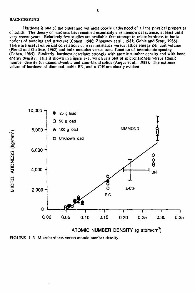
Hardness is one of the oldest and yet most poorly understood of all th_ physical propertiesof solids. The theory of hardness has remained essentiaily a semiempirical science, at least untilvery recent years. Relatively few studies are available that attempt to relate hardness to basicnotions of bonding and structure (Cohen, 1956; Zhogolev et al., 1981; Goble and Scott, 1985).There are useful empirical correlations of wear resistance versus lattice energy per unit volume(Piendl and Gielisse, 1962) and bulk modulus versus some function of interatomic spacing(Cohen, 1985). Similarly, hardness correlates strongIj with atomic number density and with bondenergy density. This is shown in Figure 1-3, which is a plot of microhardness versus atomicnumber density for diamond-cubic and zinc-blend solids (Angus et al., 1988). The extremevalues of hardness of diamond, cubic BN, and a-C:H are clearly evident.
10,000-_ • 25gload Trl 50 g load 1"
/
8,000- _ 100 g load DIAMONDE.E 0 Unknown load .L
m 6,000
iii
z to grr 4,000<"!- O
o 4_ 0'_ 2,000 a-C:H
0 = w 10. 00 0.05 0.10 0.15 0.20 0.25 0.30 0.35
ATOMIC NUMBER DENSITY (g atom/cm_)FIGURE 1-3 Microhardnessversusatomic numberdensity.
1990017647-023

9
Hlah=Pressure Synthesis of Diamond I_Kd.._.JlJ_d_
The GeneralElectricCompany was thefirsttoreveala successfulprocessforgrowthofdiamondathighpressureand hightemperature(Bundyetal.,1955),Graphiticcarbonsinth_presence of a liquid metal solvent-catalyst are brought into the temperature-pressure range wherediamond is the thermodynamically stable phase and crystals spontaneously nucleate and grow(Figure !-4). Since 1955 the growth of abrasive grain up to about 1 mm at high pressures andtemperatures has matured to become a routine manufacturing procedure. About 90 percent ofindustrial diamond abrasives are now synthesized. In terms of size, shape, and toughness, theprocess provides a reproducibility and tailorability not found in natural materials. GeneralElectric, DeBeers, Sumitomo, and the Soviet Union now provide high-pressure grit on the worldmarket.
I _PT 7/80- __] _" -
RH
Oiamond60 FE -
IZ_BERMAN-SIMON
Graphite20_//
O' I iI0 1000 2000 3000
T (K)
FIGURE 1-4 Equilibrium phase diagram for the carbon system. The P-T curves for severaldiamond-liquid metal eutecdcs are cross-plotted on the diagram. These curves define theminimum P-T conditions for high- pressure diamond synthesis by the solvent-catalyst method.The region for vapor=growth of diamond is located at pressures less than I bar and temperaturesless than 1400 K.
The pressure range for high-pressure synthesis is generally 50 to 65 kb; the temperaturerange is from ! 300 to 1700"C. The reaction mixture contains carbon (usually as graphite) incombination with the Group 8 elements, iron, nickel, and cobalt; manganese, aluminum, andboron are principal secondary elements. At the reaction conditions these systems exhibit adiamond-liquid two-phase region. Nucleation of diamond is rapid once the metal-carboneutectic temperature is exceeded.
1990017647-024
10
High-pressurediamondsynthesisisa batchoperation.The timecycleisdeterminedbythedesiredgrainsizeand optimizationofdielife.Growth ratescan be veryfast,but I000_m/hour isa usefulaveragerateforgrainsizesintherangeof 50 toI000_,m.The processbecomesprohibitivelyexpensiveforsizeslargerthanaboutI ram,withthepossibleexceptionofcrystalslargerthanIcarat.Sinteredmaterialsareproducedforcuttingtools,wire-drawingdies,and well=drillingbits.Polycrystallinepiecesup toabout50 mm indiameter,usuallyon a carbidebaseorwithina carbidering,areavailable.
It is possible to grow large gem-quality single crystals by a high-pressure thermal gradientprocess. Diamond crystals as large as 1i carats with a maximum dimension of 17 mm have beenreported (Shigley, 1987). Crystals doped with either boron or nickel can also be produced.Sumitomo Corporation sells N-doped crystals at least 6 to 7 mm in maximum dimension forfabrication into cutting tools, microtome and scalrel blades, wire dies, anvils, and heat sinks.
Similar processes are used for cubic BN synthesis. The principal solvent-catalysts arealkali and alkaline earth metal nitridez and metal solvents similar to these used for growingdiamond. Although cubic BN abrasive grain has been available since 1957, the first optically andelectrically useful crystals were synthesized in 1987 (Mishima et al., 1987).
Metastable Diamond Growth
Metastable phases can form from precursors with high chemical potential if the activationbarriers to more stable phases are sufficiently high. As the precursors fall in enet'gy they can betrapped in a metastable state. For metastable diamond synthesis the undesired competingprocesses are nucleation of graphitic carbons and graph:,tization of existing diamond. Thepossibility of making diamond in the pressure-temperature range where it is thermodynamicallyunstable has been recognized for many years (Bridgman, 1955, Lander and Morrison, 1966);however, accomplishing practical low-pressure processes has taken decades tc accomplish.
The first documented successful effort to grow diamond from vapor was initiated in 1949by William G. Eversole at the Linde Laboratories of Union Carbide Corporation (Kiffer, 1956;Sversole, 1962). Eversole's work was contemporaneous with the earliest studies of high-pressurediamond growth. Angus in the United States (Angus et al., 1968) and Deryagin in the SovietUnion (Deryagin et ai., 1968) continued these efforts, which ultimately led to proof that diamondcould be grown by chemical vapor deposition from hydrocarbon gases and to some under-standing of the role of hydrogen in the process. Although relatively rapid transient growth rates(0.1 j,m/hour) of diamond were achieved in these early studies, graphite..: carbons eventuallynucleated on the diamond seed crystals, suppressing further diamond growth. Average growthrates were too low to be,of commercial significance,
Several reviews describing the history of low-pressure diamond growth are available(Devries, 1987; Badzian and Devries, 1988; Angus and Hayman, 1988). These papers provideextensive bibliographies.
VAPOR GROWTH OF DIAMOND
The first reports of rapid low-pressure growth of diamond crystals on nondiamondsubstrates were by Deryagin's group in the Soviet Union (Deryagin eta!., 1977; Spitsyn et al.,1981); however, the method of growth was not revealed. Worldwide interest in Iow-pressulediamond growth was stimulated by a series of remarkable papers published by workers associatedwith the National Institute for Inorganic Materials (NIRIM) in Japan (Matsumoto, 1985;
1990017647-025

11
Matsumoto et al., 1982a,b; 19g7a,b). Yaichiro Sato and Nobuo Setaka were leading figures in thiseffort. Methods for growth of d_amond at rates of 10 _,m/hour were described, and convincingcharacterization evidence was given. The de novo growth of faceted diamond without thenecessity of a seed crystal was a significant advance over earlier methods.
Crystalline diamond can be grown by an astonishingly large variety of energeticallyassisted chemical vapor deposition processes. These may be conveniently, if somewhatarbitrarily, divided into two broad categories:
• Thermally-assisted chemical vapor deposition, for example, hot-filament-assistedpi ocesses.
• Plasma-assisted chemical vapor deposition (PACVD), for example, microwave- Jassistedprocesses.
These methods are described in detail late; in this report. They can produce polycrystallinediamond films on a wide variety of substr,_tes without the .necessity of a diamond seed crystal.Although detailed molecular mechanisms are rot known with certainty, all of the processes haveelements in common; namely, the presence of atomic hydrogen and the production of energeticcarbon-containing fragments under conditions that _upport high moEilities on the diamondsurface.
Average growth rates of polycrystailine diamond films are tens of micrometers per hour,but growth rates on the order of hundreds of micrometers per hour have been reported in high-energy systems. (Kurihara et al., 1988). Indeed, a growth rate of 30 to 40 _m per hour has beenachieved with an acetylene torch (IJirose and Kando, 1988; Hirose, and M;tsuizumi, 1988).Diamond-on-diamond epitaxy has been reported (Spitsyn et al., 1981; Fujimori, 1987) but theepitaxial layer is not of high quality, with stacking faults, twins, and even microcracks along(11 I) planes. It is expected that hcteroepitaxy of diamond will _ a:complishe_ in the nea,"future. The uncontrollable nucleation of diamond nuclei has prevented the g:owth of large (i.e.,greater than I ram) single crystals by vapor deposition.
DIAMOND-LIKE MATERIALS
Related research has led to the discovery of _.new class of materials, the diamond-likesolids. The diamond-like phases are distingaished by unusual hardness and chemical inertness.These properties apparently arise from the high proportion of spa carbon sites. Several recentreview articles give access to this literature (Angus and Hayman, 1988; Tsai and Bogy, 1987;Angus et al., 1986).
There appear to be two classes of diamond-like phases: the diamond-like hydrocarbons(a-C:H) and the diamond-like carbon (a-C). More is known abo_t the diamond-likehydrocarbons than the diamond-like carbons. The diamond-like carbons may, in fact, includeseveral different types of structures ranging from microcrystalline diamond to complex,amorphous materials containing significant amounts of both spz and spa carbon sites.
The diamond-like materials are made by energetically assisted deposition processes--iorexample, from rf plasma, s-by direct deposition from low-energy (-100 eV) ion beams or bycondensation from plasma arcs. As in the case of vapor growth of diamond, detailed molecularmechanisms are not known with certainty. However, evidence from several sources suggests thatthe metastable, amorphous diamond-like structures may be stabilized by the quenching due to thecold substrate.
1990017647-026

12
APPLICATIONS
Aovlication_ of Diamon_
The applications of diamond will stern from its extreme properties. Diamond has thehighest values of atomic number density, hardness, thermal conductivity at 298 K, and elasticmodulus of any known material (Table !-2). It is the most incompressible substance known andhas a thermal expansion coefficient lower than Invar. Diamond also has a high refractive indexand optical dispersion. If nitrogen is absent, diamond is extremely transparent from 230 nm to atleast 40 _,m in the infrared (apart from a few intrinsic absorption bands from 2.5 to 6.0 #m).
Applications of diamond as an abrasive or as a cutting tool arise from its extremehardness and high :hermal conductivity. The ability to deposit diamond films over large areaswill greatly expand these applications and should lead to many others as well. Diamond filmsmay find application as wear-resistant coatings, wire-drawing dies, coatings for drills, andbearing surfaces. It may also be possible to employ diamond coatings as impact-protectioncoatings for rain erosion and small-particle impact.
TABLE I-2 Some Properties of Natural Type IIA Diamond and Vapor-Grown Diamond
Properties Type IIA Vapor-Grown
Hardness, GPa ,,90* 80 - >90Mass density, g/cm a 3.515 2.8 - 3.5Molar density, g-atom/cm 3 0.293* 0.23 - 0.29Specific heat at 300 K, J/g 6.195Debye temperature, 273-1100 K 1860 ± l0 KThermal conductivity at 198 K, _,20' I0 - 20
W/cm/_Bulk mod_lus, N/m z 4.4-5.9xi011.Compressibility, cma/kg 1.7x 10⁻⁷**Linear thermal expansion coefficient 0.8xl0 -6.**
at 293 K, K"tRefractive index at 589.19 nm 2.41726 ,,2.4Dielectric constant at 300 K 5.7,0.05 ,,5.7
*Higher than any other known material.**Lower than any other known material.
***Lower than lnvar.
The high thermal conductivity, low expansion coefficient, a', strength of diamondprovide high resistance to thermal shock. Windows for very-high-po_ter lasers may takeadvantage of this combination of propertles. Crystailume for example, has announced thecommercial availability of 6-ram diameter x-ray windows. The high thermal conductivity has ledto the use of diamond as a heat sink material in electronic applications. This application, andmany others, will likely be expanded by the availability of large-area diamond films.
1990017647-027

13
Naturaland high=press_iresyntheticdiamondsarealreadyusedasinstrumentwindows inspecializedresearchapplications.Thisisa natura!applicationof vapor-growndiamondfilms;opticalelementsanddiamond=costedopticsarelong=rangepossibilities.However,someapplicationsrequiresignificantreductionsinsurfaceroughnessand inopticalabsorption.
Diamond electronic: is another long-range possibility. Diamond is a wide=band=gapsemiconductor (5.5 eV) and, furthermore, has a high breakdown voltage (~i07V/cm) and asaturation velocity (2.7 X 107 cm/sec), higher than silicon, GaAs, or InP. Electron and holemobilities are approximately 1900 and 1200 cma/V-sec respectively. However, *,heuse of vapor-grown diamond as an active electronic component will require greater crystalline perfection thanis now available. Many electronic applications will also require growth of heteroepitaxialdiamond films, which at this time has not been achieved.
Annlications of Cubic BN. SIC. and Olher Materlal_t
Cubic BN has a hardness second only to diamond and is unreactive with alloys of iron,nickel, and cobalt. These properties have led to important applications as an abrasive. It haspotential applications as an active semiconductor device (it can be doped both n- and p-type) andas a heat sink material.
Silicon carbide is a commercially important abrasive material that can be mlide in tonnagelots at I atm pressure. Recent advanc,es in the growth of large single crystals of SiC may lead toapplications as an active electronic device material, as a heat sink, and possibly as a substrate forthe heteroepitaxial growth of diamond from the vapor.
Boron carbide is used as an abrasive (although never achieving its initial promise in thisapplication), as an energy-absorbing material in armor, and as a moderator in nuclear reactors. Itis under serious study and shows promise for high-temperature thermal electric applications.
Annlications of Diamond=Like Materials
As with crystalline diamond, the applications of the diamond=like materials stem fromtheir extreme properties. Of particular importance are their hardness, chemical inertness,smoothness, and apparent impermeability. Also, these films can be deposited on cold,temperature-sensitive substrates (e.g., hardened steel), which opens up other potentialapplications.
The properties of the diamond-like hydrocarbons can be "tuned" by adjusting thehydrogen composition and by adding other functional groups. It may be possible to exploit thisbehavior to tailor the properties for specific applications.
The diamond-like materials may find principal applications as a wear-resistant coatingand as a diffusion barrier and corrosion=resist,nt coating. Coatings on magnetic and optical disksare the most immediate possibilities. Hermetic coatings to protect optical fibers and high-temperature supercondue, tors are other potential applications. These materials have been used asantireflection coatings on germanium optics because of their hardness and the ability to controltheir refractive indexes by varying the carbon/hydrogen ratio.
Diamond-like materials are being actively developed for high-resolution submicrometer-scale lithography. Excimer laser etching has been used to produce structures as small as 0.13 _,m.These materials can also be employed as a bottom layer in a two-layer resist system.
1990017647-028

14
Other potential applications of diamond-like films include )_ltraviolet-absorbing coatingsa,_d coatings for photothermal energy conversion and photoreceptors.
INTERNATIONAL ACTIVITIES
It is difficult to make an accurate assessment of the relative positions of the variouscountries known to be doing research in diamond and diamond-like materials. Groups in Japanare leading in practical applications of this new technology. Whether or not they have anygreater insight into the fundamental issues of nucleation and growth is much less clear.According to an article in the New York Times (October 20, 1988), American expertsacknowledge that Japan now holds a commanding lead in CVD diamond technology. Statisticsfrom industry sources provide a comparison: in the past 5 years, of 573 patents granted in thenew diamond technology, 488 were awarded to Japanese companies and only 28 were awarded inthe United States. Soviet workers, particularly Deryagin's group, have a long history in low-pressure diamond research (Badzian and DeVries, 1988). However, the committee is aware of noapplications of this technology in the Sovi©t Union. This may, of course, be due to theunwillingness of Soviet researchers to divulge detailed descriptions of their efforts. DeBeers hassupported low-pressure diamond synthesis, at least sporadically, since the early 1970s andcurrently is supporting work on CVD growth of diamond in both England and South Africa, butapparently not at the intensity of the Japanese effort.
Leadership in diamond-like technology appears to be more evenly diffused. There areleading research groups in Japan, the Federal Republic of Germany, Australia, Great Britain, andthe United States.
RESEARCH AND DEVELOPMENT ISSUES
The new diamond science and technology transcend the boundaries of traditionalmaterials science. Fundamental developments in this field will require _ontributions fromorganic chemistry, surface chemistry, plasma physic_ and chemistry, theoretical quantumchemistry, thin-film mechanics, and solid-state physics. A host of engineering and applieddisciplines will be involved in applications work.
The basic molecular mechanisms involved in both nucleation and growth of diamond arenot well understood. Special attention should be paid to those surface spectroscopies that cangive insight into species and processes on the growing crystal surface. It is unlikely that high-rate growth of optical- and semiconductor-grade diamonds can be achieved without betterunderstanding of the molecul3r mechanisms involved in both nucleation and growth.
Virtually all current research efforts involve growth of diamond from the vat or. Otherlow-pressure processe._--for example, growth from liquids--should be explored as alternativeavenues for growth of large, high-quality diamond crystals.
The vapor growth of diamond for sophisticated optical and electronic applications bycurrent techniques is limited by two factors: (a) the uncontrolled formation of independentdiamond nuclei during growth and (b) the appearance of growth errors during extension of thelattice. The first leads to polycrystalline films with a typical crystal size of 1 to 10 _m andsurfaces that are faceted. The second leads directly to defect structures within the diamondlattice.
1990017647-029

15
Diamond-on-diamond epitaxy has been achieved, and the epitaxial layers are approachingelectronic-grade quality. The relationships between growth parameters and the types of defectstructures produced should be explored. Heteroepitaxy on silicon, SiC, or other sacrificialsubstrates would also be highly desirable but has not been achieved yet as far as the committeeknows. Also, achieving substitutional n-type doping in diamond is still problematical.
Fundamental theoretical studies of the types of molecular structures that lead to"hardness"and basic studies of the atomic-scale processes during inelastic deformation areappropriate. This research could lead to new superhard materials and to designed modificationsof existing superhard materials.
The scale-up and engineering of plasma processes for production of diamond anddiamond-like films is important for the development of practical, large-scale applications. Rapidgrowth of uniform, high-quality films over large areas that exhibit good adhesion to theirsubstrates will be required for many applications. Here the application of fundamental conceptsof plasma chemistry and plasma physics is in order. The deposition of crystalline diamond filmsat low temperatures (<300"C) would permit a host of applications involving temperature-sensitive substrates. Deposition on steel or Gther metals, of strongly adherent films would be amajor achievement in saws, drills, avd similar tools.
Growth of diamond at high pressures will continue to be an important commercialprocess. Basic research in the synthesis of diamond and related materials at high pressures shouldbe supported.
The diamond-like phases should be recognized as a new class of materials. Much work onthe influence of elemental composition and process variables on the styucture and properties ofthe diamond-like hydrocarbons (a-C:H) is required before these materials can be fully exploited.Current a-C:H films are highly compressively stressed and are thermally unstable above 400"C.The structure and properties of the diamond-like carbons (a-C) and their relationship tomicrocrystalline diamond should be explored.
Assuming solutions to adhesion problems, the largest impact of the diamond-like phasesmay be in tribological coatings and as diffusion barriers. However, the influence of additionalelements, functional groups, and ambient gases on friction and wear characteristics is not known.The permeability of diamond-like hydrocarbons is expected to be very low. However, carefulmeasurements of permeabiK_y as a function of process conditions and film composition have notbeen made.
REFERENCES
Angus, J. C., and C. C. Hayman. 1988. Low-pressure, ,T,e_table growth of diam,_nd and"diamond-like" phases. Science, Voi. 24 !, pp. 913.-92i.
Angus, J. C., C. C. Hayman, and R. W. Hoffman. 1988. Diamond Optics, SPIE Symposium 969,August 16-17, 1988, San Diego, California. Bellingham, Washington: SPIE-lnternationalSociety for Optical Engineers.
Angus, J. C., P. K.oidl, and S. Domitz. 1986. Carbon thin films. Chapter 4 in Plasma Depositionof Thin Films, J. Mort and F. Jansen, eds. Boca Raton, Florida: CRC Press.
Angus, J. C., H. A. Will, and W. S. Stanko. 1968. J. Appl. Phys., Vol. 39, p. 2915.ItP
1990017647-030

16
Badzian, A. R., and R. C. Devries. 1988. Crystallization of diamond from the gas phase i. Mat.Res. Bull., Voi. 23, p. 385.
Bridgman, P.W. 1955. Synthtic Diamonds. _i. Am., Vol. 193, p. 42.
Bundy, F. P., H. T. Hall, H. M. Strong, and R. H. Wentorf, Jr. 1955. Man-Made Diamonds.Nature, Vol. 176, p. 51.
Cohen, M. L. 1986. Predicting new solids and superconductors. Science, Vol. 234,pp. 549-553.
Cohen, M.L. 1985. Calculation of bulk moduli of diamond and zinc-blende solids. Phys. Rev.B. Condensed Matter, Vol. 32, No. 12, pp. 7988-7991.
Deryagin, B. V., B. V. Spitsyn, L. L. Builov, A. A. Klochkov, A. E. Gorodetskil, and A. V.Smolyaninov. 1977. Diamond crystal synthesis on nondiamond substrates. SOy. Phys.Dokl., Vol. 21, p. 676.
Deryagin, B. V., D. V. Fedoseev, V. M. Lukyanovich, and 1_.V. Spitzin_ 1968. FilamentaryDiamond Crystals. J. Cryst. Growth, Vol. 2, p. 380.
DeVries, R.C. 1987. Synthesis of diamond under metastable conditions. Ann. Rev. Mater. Sci.,Vol. 17, p. 161.
Eversole, W.G. 1962. U.S. Patents 3,030,187 and 3,030,188.
Fujimori, N. 1987. Symposium N: Plasma-Assisted Deposition of New Materials. FinalProgram and Abstracts of the Materials Research Society Meeting, Boston, November 30-December 5, 1987.
Goble, R. J., and S. O. Scott. 1985. Canadian Mineralogist, Vol. 23, pp. 273-285.
Hirose, Y., and K. Kondo. 1988. Abstracts of Spring Applied Physics Lab. Meeting, Mar. 1988,. p. 434.
Hirose, Y., and M. Mitsuizumi. 1988. New Diamond (in Japanese), V. 4, p. 34.
Kiffer, A. D. 1956. Synthesis of Diamond From Carbon Monoxide. Tonowanda Laboratories,Linde Air Products Co., Tonawanda, New York.
Kurihara, K., K. Sasaki, M. Kawaradi, and N. Koshino. 1988. High rate synthesis of diamondby dc plasma jet chemical vapor deposition. Appl. Phys. Lett., Vol. 52, p. 437.
Lander, J. J,, and J. Morrison, 1966. Surface Science, Vol. 4, p. 241.
Matsumoto, S. 1985. J. Mat. SCi. Lett., Vol. 4, p. 600.
Matsumoto, S., M. Hino, and T. Kobayashi. 1987a. Chemical vapour deposition in RF glowdischarge. Appi. Phys. Lett.,Vol. 51, p. 737.
Matsumoto, S._ S. M. Hino, and T. Kobayashi. 1987b. Synthesis of diamond films in a RFinduction thermal plasma. Paper $7-03, 2458, presented at the Eighth InternationalSymposium on Plasma Chemistry (ISPC-8), Tokyo, Japan.
1990017647-031
17
Matsumoto, S., Y. Sato, M. Kamo, and N. Setaka. 1982a. Vapor deposition of diamond particlesfrom methane. Jpn. J. Appl. Phys., Part 2, Vol. 21, p. 183.
Matsumoto, S., Y. Sato, M. Tsutsumi, and N. Setaka. 1982b. Growth of diamond particles frommethane-hydrogen gas. J. Mat. Sci., Vol. 17, p. 3106.
Mishima, O., J. Tanaka, S. Yamaoka, and O. Fuku:,maga. 1987. High-temperature cubic boronnitride p-n junc2ion diode made at high pressure. Science, Voi. 238, pp. 181-183.
Plendl, J. N., and P. J. Gileisse. ]962. Phys. Rev., Voi. 125, pp. 828-832.
Shigley, J. E., et al. 1987. The gemolog;cal properties of the DcBeers gem-quality syntheticdiamonds. Gems and Gemology, _Vol.23, pp. 187-206.
Spitsyn, B. V., L. L. Bouilov, and Ft.V. Deryagin. 1981. Vapor growth of diamond on diamondand other surfaces. J. Cryst. Growth, Vol. 52, p. 219.
Tsai, H., and D. B. Bogy. 19,.7. Characterization of diamondlike carbon films and theirapplication as overcoats on thin-film media for magnetic recording. J. Vac. Sci. Tech.,Vol. A5, p. 3287.
Yalamanchi, R. S., and G. K. _',,:.Thutupalli. 1988. Investigations of R. S. plasma-depositeddiamond-like carbon coatings. J. Thin Solid Films, Voi. 164, pp. 103-109.
Zhogolev, D. A., O. P. Bugaets, and J. A. Marushko. 1981. Zh. Struktur Khim. Vol. 22, No. 1,pp. 46-53.
1990017647-032

2
GROWTH PROCESSES
This chapter addresses deposition processes of superhard materials as defined inChapter I. Although it is the discovery of diamond growth from a low-pressure vapor byenhanced CVD techniques that is the focus of this report, the wider range of materials andme_.hods is also described.
The high-temperature, high-pressure (HPHT) techniques for growth of diamond andcubic BN, which are now over 30 years old, can be considered a mature technology. However,there are still some key scientific questions relating even to basic nucleation and growth andpotential technological developments (large-area single crystals with controlled purity andperfection) that must still be explored. If homoepitaxy of diamond proves to be important, anin-country capability, or at least expertise, in the preparation of HPHT substrate may be critical.
It is the control of nonequilibrium gas phase chemistry that allows for the growth ofdiamond at low pressures. Over the past I0 years workers have moved from a generally heldbelief that no practical process for low-pressure diamond growth was possible to the currentrealization that nearly any method that produces a ready supply of atomic hydrolsen and somecarbon-containing species works. Furthermore, the crystal quality and related morphology areremarkably similar for all the various processes and their variants, even though they range fromplssma-enhanced processes to heated-filament-assisted nonplasma processes. During the courseof the writing of this report even an atmospheric oxyacetylene torch has been repor'^d to producepolycrystalline diamond films+ Such observations suggest a common mechanism eL _c'eation andgrowth. However, there are differences, such as the growth rates reported varying ove_ 3 ordersof magnitude (0.1 to 300 _m/hr). Also, scratching the substrate with diamond (or other abrasive)is essential for high nucleation densities y,l/_m') in some processes but not others (e.g., thermalplasmas and atmospheric torch). To compare the various deposition techniques, much more needsto be known about the generation and transport of critical vapor species to the growing filmst_rface as well as surface processes during both nucleation and growth.
Key technological concerns include the deposition rate, the area that can be uniformlycovered, the throwing power of the process, the range of substrates on which diamond cannucleate, the substrata temperature, and the energy efficiency of the process. Eventually acomparative parameter such as the mass deposited per unit time per unit power input could beu_ed to compare each of the processes on an economic basis, but results are currently too sketchy.Also, each application will weight the different components of such a parameter differently.
19
1990017647-033
2O
Although enhanced CVD processes for diamond growth have created a number of newapplication opportunities, there are a number of limitations. These include (a) the high substratetemperature (~ 1000"C) for optimum crystal perfection; (b) the large grain size, which leads tooptical and IR scattering, high friction, etc.; (c) contamination from etching and re-deposition ofthe substr_te and deposition system components in contact with the atomic hydrogen; (d) thehigher defect densities reported in all CVD diamond; (e) diamond's low coefficient of thermalexpansion compared to most sabstrate materials; (f) lack of adhesion; (g) high stress; and (h) lackof large area heteroepitaxial substrates. Certainly the hope is that, through further developmentof current techniques plus discovery of even other deposition processes, these problems can beovercome. Of course, in formulating new applications for CVD diamond it is well to keep inmind basic limitations that are inherent for diamond materials in general. For example, theupper use temperature for conventional diamonds in air is no more than approximately 600 to700"C, and a similar limitation is expected to apply to CVD-grown material.
For many applications the substrate temperature is the limiting factor, and oftentemperatures above 500"C are unacceptable. A number of physical vapor deposition (PVD)techniques, involving ion bombardment, have been developed over the past 18 years to producethese materials at close to room temperature. However, the DLC and DLHC have lowercrystal!inity, higher residual stress, and lower hardness. To their credit, DLC and DLHC filmsare smooth, dense, and reasonably hard and have a variable range of other properties such asrefractive index, optical band gap, and electrical resistivity. A relatively unexplored area ofdeposition "space" is the use of both bombardment and chemical vapor deposition processessimultaneously at temperatures not exceeding 300 to 500"C. Such materials may have propertiesintermediate between the diamond and DLC and DLHC materials, possibly leading to newapplications.
One final research and development (R&D) opportunity is the possibility ofpolycrystalline cubic BN films with grain size similar to that of diamond films. Whetheranalogous approaches might be successful remains to be seen. Microcrystalline cubic fiN hasbeen produced by ion-bombardment-mediated PVD processes (similar to DLC and DLHC), andthis provides some hope. However, no successfu! attempts have been reported for crystallinecubic BN.
GENERIC AND FUNDAMENTAL ISSUES
The two principal superhard materials, diamond and cubic BN, can be synthesized byhigh-pressure, high-temperature (HPHT) processes in the stable thermodynamic region by staticor dynamic methods in the case of diamond, or by low-pressure techniques in regions ofthermodynamic metastability. The former is a mature manufacturing process and will bedescribed first. About 90 percent of all industrial diamond used is synthesized by the HPHTprocess because it prm, ides a reproducible product in terms of size, shape, and toughness (orfriability). All cubic BN must be synthesi_ed, since it does not occur naturally. Research anddevelopment effort in certain areas of this field in the United States appears to be very limitedcompared to activities in some other countries.
The vapor deposition of diamond now allows for preparation in many new forms--thinfilms over large areas, chemically bonded to a wide range of surfaces, on complex shapedsurfaces, freestanding forms, powders, etc. It appears that cubic BN films with large crystal sizes(>1 _,m) are possible, which would open Ul_even further new materials opportunities. Severalyears ago it seemed as if polycr_stalline films of diamond at practical growth rates could not beprepared at all, and now it appears that just about every technique that can provide an intensesource of atomic hydrogen during growth works. This creates the frustrating situation of having
1990017647-034

21
too many choices. Ultimately it may turn out that there is no one best deposition method butrather that certain ones will be best for certain film forms or applications.
This section deals mainly with diamond and diamond-like materials--i.e., amorphous antinanocrystalline carbon both with and without hydrogen and with high gram-atom numberdensities (p_ > 0.2 g-atom/era s) (Angus et al., 1986)--since they are the only superhard materialsfor which a significant body of literature exists. The limiting value of hardness of DLC andDLHC films is sti!l not known. Cubic BN has been prepared as a microcrystalline coating, but todate no films with crystal sizes above 200 A have been reported, and the chemical and structuralcharacterization of these materials is sketchy. The recent disclosure of a suboxide of boron ofnominal composition of B_20 (Badzian, 1988) as a material that can scratch diamond is alsointriguing. This composiUon also can be prepared by reactive sputtering to have propertiessimilar to that of the bulk material. However, such reports must be considered with caution,since even SiC has been known to scratch diamond. Superhard materials in the C-N system areyet to be explored.
If cubic BN can be successfully vapor-deposited as large crystals and polycrystaUinefilms, it is expected that research on this material will increase dramatically, just as whendiamonds were successfully deposited from the vapor and the result recognized. Depositionapproaches analogous to those for diamond are under way in the United States and elsewhere.
In this report the deposition of superhard materials is categorized in a standard manner aschemical vapor deposition (CVD) and physical vapor deposition (PVD) processes. In general,CVD methods use g_-phase chemistry to control both the retention of the metastable phase whencondensed on a surface and the details of the composition, impurities, defects, etc. In PVD it isusually ion bombardment processes that control the characteristics and thus the properties of theresulting metastable films. As mentioned earlier, it now seems that just about any process thatefficiently produces atomic hydrogen and carbon-containing species can yield diamond films oversome range of conditions. In some der_osition processes both physical and chemical processes takeplace simultaneously, but such distinctions will not be made specifically. Very often the relativeroles of the two different general processes are not well understood.
HIGH-PRESSURE, HIGH-TEMPERATURE PROCESSES
The first reproducible industrial process for making diamond was announced in 1955, andthe synthesis of cubic BN was accomplished by 1957. Both phases were precipitated from solutionat pressures >45 kb and temperatures >II00"C,where they are the thermodynamically stablephase. The unique chemistry for each of the two superhard materials is considered separately.A description is given of the critical mechanical equipment that makes the synthesis possible.
Materials Growth Processes
Direct Conversion
It is possible to make both diamond and cubic BN by direct conversion of graphite andhexagonal BN, respectively. This can be done both by static and dynamic processes, but fordiamond the pressure range (>i20 kb) and temperature are prohibitively high and noteconomically viable because of ',he limited life of carbide dies used in static processes. However,under dynamic conditions (shock), the conversion is practical, and the DuPont process provides amarketable product. Becattse of the short reaction time, the crystals range in size from
1990017647-035

22
submicrometer to several micrometers, and they are used primarily for polishing-grade materialor for starting material for sintering.
For cubic BN the pressure-temperature (P-T) conditions are less severe than for diamond,and a directly converted product is available. The wurtzite form of BN, which is also hard, ismade by shock synthesis and is used primarily for sintering polycrystalline aggregates.
Static or Indirect Process
The difficulties of direct conversion led to the development of processes to lower thepressure and temperature. This is accomplished by use of a solvent-catalyst system that permitsgrowth to occur at conditions much nearer the diamond-graphite equilibrium line but at lowertemperatures.
The static synthesis process consists of first raising the pressure to the desired value andthen raising the temperature of the cell by resistive heating. The P-T conditions for growth areheld for the d_sired time, and the power to the heater is decreased to zero. The pressure is thenreleased and the cell removed for separation of the product.
The P-T conditions for both diamond and cubic BN are attained as described above, butthe chemistry for the synthesis of the two materials is different. For diamond, the compositionsare generally mixtures of Group VIII metals with graphite. Usually the metals iron, cobalt, ornickel are major components of the alloy with carbon, with manganese, aluminum, and boron thesecondary components, The physical chemistry of these systems can be described in terms of aphase diagram of the selected metal alloy-carbon system (a T-X diagram) at pressures wherediamond is a stable phase in equilibrium with a metal-rich liquid. In this system there exists aeutectic at lower P-T conditions than required for direct conversion. In these terms, the growthis from solution, and the driving force for nucleation is the difference in solubility between thatof diamond and graphite under the HPHT conditions. Nucleation and growth begin as soon asthe eutectic temperature of the system is exceeded. Some believe the process is better describedas "catalytic," and the compromise term "solvent-catalyst" is frequently seen in the literature.There are still many things not understood about the nature of the solution and the transport in itunder HPHT conditions.
The first requirement is a mechanical system that will reproducibly attain 50-65 kb and1200-1700"C simultaneously. Since the material is produced in batches rather than continuously,it is an advantage to have as large a working volume as possible. There are several types ofapparatus (e.g., uniaxial belts or girdles, tetrahedral, octahedral, and variations on the cube press,piston-cylinder) and cells (e.g., low and high aspect ratio). During the more than 30 years ofexperience in synthesizing diamonds, there has been a convergence in the use of uniaxial belts formanufacturing. The other methods have advantages for R&D purposes, but scale-up hasgenerally favored the belt.
The belt consists of a central die, generally of cemented tungsten carbide, _urrounded bya serie,_ of "belted" steel rings to keep the carbide in compression. Two symmetrically opposedtapered anvils are pressed toward the die hydraulically and are separated from carbide-carbidecontact by a set of gaskets made from natural cr synthetic pyrophyllite or soapstone-like material(Figure 2- I).
Carbide and pyrophyllite are the key materials used in this and most other high-pressureapparatus. The gasket provides mechanical, thermal, and electrical insulation and contains thecell and its reactants. The anvil-die-anvil combination is adapted to commercially availablepresses. The cost of setting up a large apparatus is estimated to be in the range of at least
1990017647-036

23
$250,000 to $1,000,000. This equipment must be capable of repeated excursions to and fromHPHT conditions. Die breakage is :elated to fatigue and work-hardening of the carbide dies andcan be an important manufacturing cost factor. The supply and cost of carbide dies (esneciallyfor large volume) are probably key factors in limiting new entrants to the manufacturing of thesematerials. The attractiveness and relative simplicity of CVD as alternative processes will beobvious, as described later in this report.
i
i
FIGURE 2-I The Hall "belt" apparatus. Shaded areas are cemented carbide; black is gasketmaterial.
There are many celi designs to cover the needed variations, but common to all is internalheating by passing a low-voltage high current through the cell. Direct heating usually means thecurrent passes directly through the reactants (e.g., a mixture of iron and graphite for diamondsynthesis). Indirect heating is used with nonconducting reactants (e.g., BN plus Li3N mixture forcubic BN) by packing them in a conducting cylindrical sleeve or around a condccting core(graphite or metal). Cell variations result from the need to separate reactants from containers andto control the heat distribution.
1990017647-037

24
Cubic BN Chemistry
The solvent-catalysts for cubic BN are based primarily on alkali or alkaline earth metalsand their nitrides. "[he phase diagram for hexagonal BN with Li3BN z is analogous to that ofgraphite with a metal. Cubic BN can also be synthesized from Group VIII metals with a bit ofaluminum added and from other systems, but the water and acid solubility of the alkali andalkaline earth metals and nitrides favors easy removal of the product from these reactants.
Control of Crystal Size
The static process permit:, control of grain size simply by _,ontrolling the time the systemremains at the desired P-T conditions. Carbon is transported from the graphite source through athin metal film to the growing crystal. Most abrasive grain found in the marketplace is less than!mm in maximum dimension because the process becomes noneconomical if the growth time istoo long. The practice has been to use sintered diamond when sizes greater than 1 mm areneeded. The special case of large gem-quality crystals is considered below. Growth rates can bevery high, but 1 mm per hour is commonly attained.
The nucleation rate can be controlled by varying pressure conditions above the eutectictemperature for both diamond and cubic BN. Nucleation can also be controlled by seeding withsmall diamond or cubic BN crystals.
Growth of Large Crystals
In 1970 a thermal gradient process for growing large crystals (:, 1 ram) in a controli_.dmanner was developed (Figure 2-2). Using this technique, colorless, blue (B-doped), and yellow(N-doped) diamond crystals of gem quality were grown to about 6 mm in maximum dimensionand about 1.3 carats weight. The crystal size at that time was primarily limited by cell size.These crystals were grown one at a time for 100 hours or more. Sin:e that time Sumitomo andDeOeers have both scaled up the process to grow larger crystals and many at a time. Yellowcrystals up to 7 mm in size are available (from $umitomo Electric) for tools, windows, scalpels,anvils, etc. DeBeers has reported a crystal greater than I! carats with a maximum dimension of 17ram. The process requires large expensive equipment, which could be producing abrasive grain,so that some manufacturers have been reluctant to get involved. To improve the yield, manycrystals must be grown at the same time by optimizing the use of the thermal gradient verticallyin the cell of a belt apparatus. The gradient can be established in the cell with a sleeve heater,but then alloys with different eutectic temperatures must be used to allow growth in severallayers in the cell. This is fairly siml_le for N-doped ¢rysta|s, but there are fewer degrees offreedom for the aluminum alloys used to eliminate nitrogen and produce colorless and bluecrystals. New alloy design is needed.
Cubic BN crystals to about 3 mm maximum dimension have been grown by thermalgradient methods, but good-quality untwinned crystals are rare. Sumitomo has taken up thischallenge, and this situation can be expected to change. NIRIM (Mishima, et al. :987) has growncubic BN p-n junctions.
The production of large crystals is of considerable current interest for electronic, optical,and dielectric applications and should be re=evaluated in the United States, especially in light ofthe obvious commitment by Japanese and ,South African diamond manufacturers. However, ifthe CVD techniques continue to show promise, the difficulty of growth at high pressures may bebypassed as epitaxial techniques (perhaps on SiC crystals) are developed.
1990017647-038
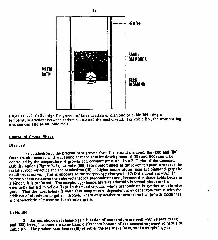
25
H(ATER
SMALLOlAMONOS
METALBATH
SEEDOIAMOHO
FIGURE 2-2 Cell design for growth of large crystals of diamond or cubic BN using atemperature gradient between carbon source and the seed crystal. For cubic BN, the transportingmedium can also be an ionic melt.
Control of Crystal Shl_oe
Diamond
The octahedron is the predominant growth form for natural diamond; the (100) and (il0)faces are also common. It was found that the relative development of (111)and (100) could becontrolled by the temperature "_fgrowth at a constant pressure. In a P-T plot of the diamondstability region (Figure 2-3), ,ie cube (100) face predominates at the lower temperatures (near themetal-carbon eutectic) and the octahedron (111)at higher temperatures, near the diamond-graphiteequilibrium curve. (This is opposite to the morphology changes in CVD diamond growth.) inbetween these extremes the cubo-octahedron predominates and, because this shape holds better ina binder, it is preferred. The morphology-temperature relationship is serendipitous and isessentially limited te yellow Type lb diamond crystals, which predominate in synthesized abrasivegrain. That the morphology is more than temperature-.dependent is evident from results with theaddition of aluminum to getter nitrogen, where only octahedra form is the fast growth mode thatis characteristic of processes for abrasive grain.
Cubic BN
Similar morphological changes as a function nf temperature a_e seen with respect to (I]!)and (100) faces, but there are some basic differences because of the noncentrosymmetric nat,:re ofcubic BN. The predominant face is (!11)of either the (+) or (-) form, so the morphology is
1990017647-039
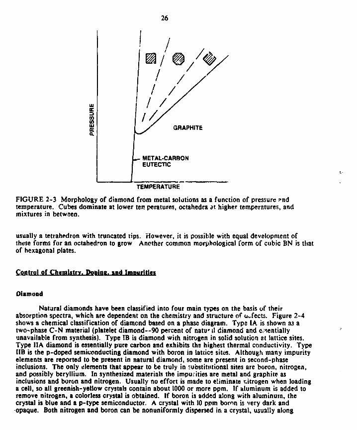
26
i/
,.- METAL-CARBONEUTEC'nC
TEMPERATURE
FIGURE 2-3 Morphology of d;amond from metal solutionsasa function of pressure_ndtemperature. Cubes dominateat lower ten peratures,octahedraat higher tempe_tures, andmixtures in between.
usually a tetrahedron with truncated tips. However, it is possible with equal development ofthese forms for an octahedron to grow Another common morphological form of cubic BN is thatof hexagonal plates.
Control of Chemistry. Doninn. snd Imnurities
Diamond
Natural diamonds have been classified into four main types on the basis of theirabsorption spectra, which are dependent on the chemistry and structure o£ u,.fects. Figure 2-4shows a chemical classification of diamond based on a phase diagram. Type IA is shown 03 atwo-phase C-N material (platelet diamond--90 percent of natu-_l diamond and e.:_entially 'unavailable from synthesis). Type IB is diamond with nitrogen in solid solution at lattice sites.Type IIA diamond is essentially pure carbon and exhibits the highest thermal conductivity. TypeliB is the p-doped semiconducting diamond with boron in lattice sites. Although many impurityelements are reported to be present in natural diamond, some are present in second-phaseinclusions. The only elements that appear to be truly in -..ubstitutional sites are boron, nitrogen,and possibly beryllium. In synthesized materials the impu._ities are metal and graphite asinclusions and boron and nitrogen. Usually no effort is made to eliminate uitrogen when loadinga ceil, so all greenish-yellow crystals contain about 1000 or more ppm. If aluminum is added toremove nitrogen, a colorless crystal is obtained. If boron is added along with aluminum, thecrystal is blue and a p-type semiconductor. A crystal with 10ppm bornn is very dark and
-opaque. Both nitrogen and boron can be nonuniformly dispersed in a crystal, usually along
1990017647-040
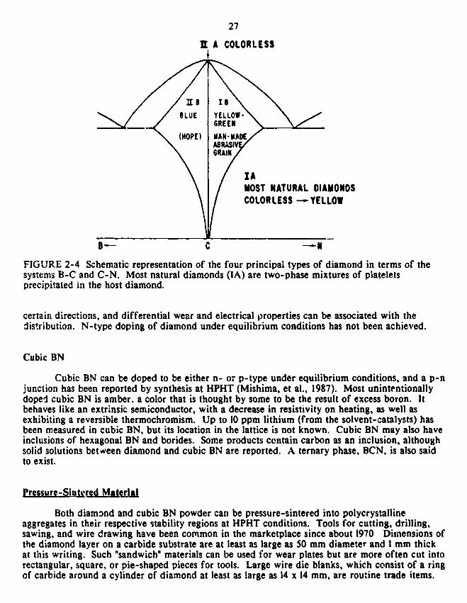
27
X A COLORLESS
YELLOW-
,r
r ZAMOSTNATURALOIAMONOSCOLORLESS-* YELLOW
B"- C ----II
FIGURE 2-4 Schematic representation of the four principal types of diamond in terms of thesystems B-C and C-N. Most natural diamonds (IA) are two-phase mixtures of plateletsprecipitated in the host diamond.
certain directions, and differential wear and electrical properties can be associated with the:listribution. N-type doping of diamond under equilibrium conditions has not been achieved.
Cubic BN
Cubic BN can be dopedto be either n- or p-type under equilibrium conditions,and a p-njunction hasbeenreported by synthesisat HPHT (Mishima, et al., 1987). Most unintentionallydopedcubic BN is amber, a color that is thought by someto be the resultof excessboron, itbehaveslike an extrinsic semiconductor,with a decreasein resistivityon heating, as well asexhibiting a reversible thermochromism. Up to 10ppm lithium (from the solvent-catalysts)hasbeenmeasuredin cubic BN, but its locationin the lattice is not known. Cubic BN may alsohaveinclusionsof hexagonalBN and borides. SomeDroductscontain carbon as an inclusion,althoughsolidsolutionsbetween diamondand cubic BN are reported. A ternary phase,BCN, is alsosaidto exist.
Pressure-Sintered Material
Both diamond and cubic BN powder can be pressure-sinteredinto polycrystallineaggregatesin their respectivestability regionsat HPHT conditions. Tools for cutting, drilling,sawing,and wire drawing havebeen commonin the marketplacesinceabout 1970 Dimensionsofthe diamondlayer on a carbidesubstrateare at leastas largeas 50 mm diameterand I mm thickat this writing. Such"sandwich"materialscan be usedfor wear platesbut are more often cut intorectangular,square,or pie-shapedpiecesfor tools. Large wire die blanks, which consistof a ringof carbide arounda cylinder of diamondat leastas largeas 14x 14ram, are rou:ine trade items.
1990017647-041
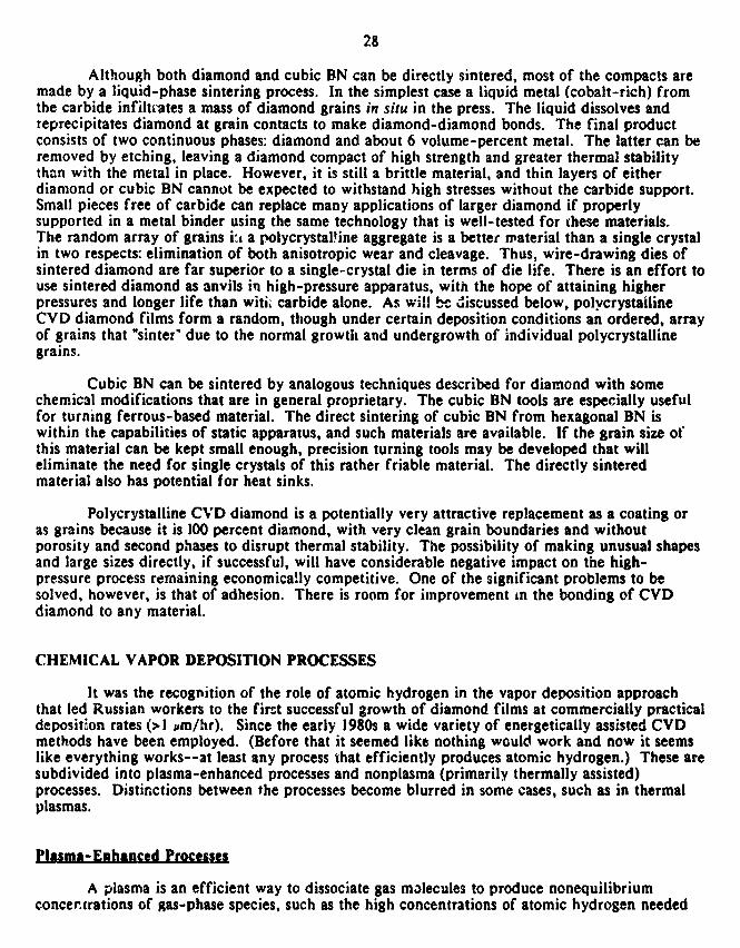
28
Although both diamond and cubic BN can be directly sintered, most of the compacts aremade by a liquid-phase sintering process. In the simplest case a liquid metal (cobalt=rich) fromthe carbide infiltrates a mass of diamond grains in situ in the press. The liquid dissolves andreprecipitates diamond at grain contacts to make diamond=diamond bonds. The final productconsists of two continuous phases: diamond and about 6 volume-percent metal. The latter can beremoved by etching, leaving a diamond compact of high strength and greater thermal stabilitythan with the metal in place. However, it is still a brittle material, and thin layers of eitherdiamond or cubic BN cannot be expected to withstand high stresses without the carbide support.Small pieces free of carbide can replace many applications of larger diamond if properlysupported in a metal binder using the same technology that is well=tested for _hese materials.The random array of grains i:_a polycrystal!ine aggregate is a better material than a single crystalin two respects: elimination of both anisotropic wear and cleavage. Thus, wire=drawing dies ofsintered diamond are far superior to a single-crystal die in terms of die life. There is an effort touse sintered diamond as anvils in high=pressure apparatus, with the hope of attaining higherpressures and longer life than witi_ carbide alone. As will be _iscussed below, polycrystallineCVD diamond films form a random, though under certain deposition conditions an ordered, arrayof grains that "sinter_due to the normal growth and undergrowth of individual polycrystallinegrains.
Cubic BN can be sintered by analogous techniques described for diamond with somechemical modifications that are in general proprietary. The cubic BN tools are especially usefulfor turning ferrous-based material. The direct sintering of cubic BN from hexagonal BN iswithin the capabilities of static apparatus, and such materials are available. If the grain size ofthis material can be kept small enough, precision turning tools may be developed that willeliminate the need for single crystals of this rather friable material. The directly sinteredmaterial also has potential for heat sinks.
Polycrystalline CVD diamond is a potentially very attractive replacement as a coating oras grains because it is 100 percent diamond, with very clean grain boundaries and withoutporosity and second phases to disrupt thermal stability. The possibility of making unusual shapesand large sizes directly, if successful, will have considerable negative impact on the high=pressure process remaining economica!ly competitive. One of the significant problems to besolved, however, is that of adhesion. There is room for improvement in the bonding of CVDdiamond to any material.
CHEMICAL VAPOR DEPOSITION PROCESSES
It was the recognition of the role of atomic hydrogen in the vapor deposition approachthat led Russian workers to the first successful growth of diamond films at commercially practicaldeposition rates (_,! j,m/hr). Since the early 1980s a wide variety of energetically assisted CVDmethods have been employed. (Before that it seemed like nothing woul0 work and now it seemslike everything works--at least any process that efficiently produces atomic hydrogen.) These aresubdivided into plasma-enhanced processes and nonplasma (primarily thermally assisted)processes. Distinctions between the processes become blurred in some cases, such as in thermalplasmas.
Plasma-Enhanced Processes
A plasma is an efficient way to dissociate gas molecules to produce nonequilibriumconcentrations of gas=phase species, such as the high concentrations of atomic hydrogen needed
1990017647-042

29
to make dia,lond. Plasmas can be generated by a number of energy sources (dc, rf, andmicrowave electric fields and flames), and the plasmas can be either cold or hot.
The main techniques with their variations are given in Table 2-I.. and schematics oftypical experimental setups are shown in Figure 2-5. Also given are representative references.Although these preparation methods are not discussed in detail, a few general comments can bemade.
The most extensively studied process is microwave plasma-enhanced chemical vapordeposition (MPECVD). This trend has only increased over the past several years, especially inJapan (Figure 2-6). The apparent reasons are (a) the stability and reproducibility of microwavecold plasmas; (b) their energy efficiency (high plasma density, low electron temperatures, lowsheath potentials); (c) the increased availability of 1-2 kW microwave (wave-guided) powersupplies and applicators; and (d) the potential to scale the process to larger substrates (4-5 in.).However, the rf and dc plasma methods produce diamond films of comparable quality and, undercertain conditions (e.g., substrate biasing), at much higher rates, and they are being used incommercial processes in the United States (Crystallume and Air Products).
Although strides to scale the MPECVD process have been made, it seems that rf and dcplasmas are easier to scale. It is not as clear which of these processes would have an advantage incoating nonplanar substrates or which is amenab!e to large batch coating such as on verticallystacked wire mesh trays for cutting tool coatings. Also, dc plasma processes at present seem tohave an advantage of potentially higher deposition rates (--SX).
The thermal plasma approach generates the necessary temperature to dissociate Hz directlyin the plasma. Although the plasma nozzle is nearby, nothing is known at present as totemperatures and carbide formation at the met_! nozzle or, more generally, the stability of theprocess. To date this process has only been used successfully in Japan by NIRIM, Fujitsu andAsahi Diamond; U.S. companies and universities are pursuing this approach. It isknown that the rates can be extremely high (200-500 um/hr) but the deposition area is small (<1cm2). The deposition "on-time" is thermally limited, and the uniformity and reproducibility arepoor. However, if controlled, this approach could be very important.
Of the remaining plasma-enhanced techniques listed in Table 2-1, the atmospheric torchis unique and potentially the most important. Although not strictly a plasma, an atmosphericflame is simple in design, cost, and use. Hydrogen, oxygen, and hydrocarbon gases (e.g.,acetylene) are simply burned, and diamond forms in the reducing part of the flame. Hirose'sresults in atmospheric torch deposition (Hirose and Mitsuizumi, 1988) have now been repeated inseveral laboratories around the world (Naval Research Laboratory, Pennsylvania State University,and Sumitomo Electric), and it is expected that other groups will be pursuing this technique.
The trade-offs among plasma stability, deposition rate, coating area, film quality (asdefined by either scientific or technological criteria) for each of the plasma processes have yet tobe determined. It is likely that there will be nos__ answer, solution, or technique; rather, eachtechnique will find its niche (albeit, some small niches).
NonDhtsma Processes
Besides the plasma-enhancement approach to vapor deposition of diamond, Derjaguin andFedoseev (1977) recognized that high-temperature and catalytic processes could also produce a"superequilibri ,'n" of atomic hydrogen, which appeared to be the necessary ingredient for asingle-step deposition process.
1990017647-043

3O
TABLE 2-1 Plasma-Enhanced Chemical Vapor Deposition (PECVD) Processes for DiamondF'_lmGrowth
DepositionRate Selected
Technique (_,m/hr) References
Microwas _-PECVD 0.1-5 1,2,3- magnetic field at high pressure (>1 torr)- ECR (_:0.1 torr)
¢rf-PECVD ? 4,5
- inductively coupled- capacitively coupled
dc-PECVD 0.0 ! - 1O0 6,7,8- capacitively coupled- hollow cathode discharge
Thermal plasmas 10-300 9,10, I1- dc therm_,! plasma torch- rf thermal plasma torch- atmospheric flame torch- vacuum arc
Key to References:
!. :',amo, M. Y. Sato, S. Matsumoto, and N. Setaka. 1983. Diamon synthesis from gas phase inmicrowave plasma. J. Cryst. Growth, Vol. 62, p. 642.
2. Saito, S., S. Matsuda, and S. Nogita. 1986. J. Mat. Sci. Lett., Vol. 5,p. 565.3. Kawarada, H., K. S. Mar, and A. Hiraki. 1987. Larbe area chemical vapour depositon of
diamond particles and films using magneto-microwave plasma. Jpn. J. Appl. Phys.,Vol. 26, p. L1032.
4. Matsumoto, S. 1985. Chemical vapour deposition of diamond in rf glow discharge. J. Mat.S¢[. Lett., Vol. 4, p. 600.
5. Marria, R., L. Stobierski, and R. Pampuch. 1981. Diamond syhthesis in cool plasma. Cryst.Res. Tech., Vol. 16, p. 785.
6. Suzuki, K., H. Yasuda, and T. Inuzuka. 1987. Growth of diamond thin films by dc plasmachemical vapor deposition. Appl. Phys. Lett., Vol. 50, no. 12, p. 728.
7. Pinneo, J.M. 1987. Diamond Technology Initiative Workshop, paper 4. Sponsored by theOffice of Naval Research at M.I.T. Lincoln Laboratories, Boston, Massachusetts(February 2).
8. Singh, B., O. R. Mesker, A. W. Levine, and Y. Arie. 1988. Diamond synthesis by hollowcathode plasma assisted chemical vapor deposition. Proc. SPlE, Vol. 877, p 70.
9. Koshino, N., K_ Kurihara, M. Kawarada, and K. Sasaki. 1988. 1988 MRS Spring Meeting,Symposium D Extended Abstracts, p. 95. M. Gels, G. H. Johnson, and A. R. Badzian, eds.
10. Matsumoto, S., M. Hino, and T. Kobayashi. 1987. Synthesis of diamond films in a FRinduction thermal plasma. Appl. Phys. Lett., Vol. 51, p. 737.
11. Hiro3e, Y., and Kondo. Spring 1988. APL Meeting, Abstracts, p. 434.
1990017647-044

31
H3 + CH3
Quartz tube/.
Wave guide $ubstrate
_"_# _ ca.*_+ Re_,--ntGas
P"Jnger
Sheath gas (S) _1 IMagnetron I .._j I
Vacuum•(a)pump t_
O RF
0 Work=oil0
Substmte ..LL
Subsb'ato w°rking c°i' To Manometer ..]_[_ _._a.r.,, SubsVate hdder J I
"_- -__"_ o"Pu,,p (a)
c.--2-[2RF genmato¢
113.56MHz1
(b)
Water J_-:i]
' iI1_ i
_=__u Plasmajet ,':i',,',
0 =ll t *# #l t t ',
bstrate , ' ' ' ' ,
1¢1 (elGas mlet
FIGURE 2-5 Schematic diagrams of various plasma-enhancedCVD techniquesfor diamondgrowth: (a) microwave PECVD (Kamo et el., 1983); (b) rf PECVD (Matsumoto, 1985); (c) dcPECVD (Suzuki et al., 1987); (d) rf thermal plasmaCVD (Matsumoto, 1985); (e) dc thermalplasmaCVD (Koshino et el., 1988).
1990017647-045

32
2O
Methods
_-- [] HF/EACVD
_ RF10 MW
_) _1_ DC
_. UV/Laser[] Other
[] Theory0
1/86 2/86 1/87 2/87
FIGURE 2-6 Statistics of abstracts published at the meetings of the Japanese Applied PhysicsSociety on different preparation methods for diamond thin films (Bachmann et al., 1988).
Other than a patent by Vicke_-y (1973) and the recent paper by Badzian eta!. (1988), theidea and use of catalytic processes in diamond vapor growth has not been explored. Theseapproaches may prove to be important from an energy (economy) viewpoint, and thus more workis justified. However, chemistry control is always difficult to unravel, and adding catalyticmechanisms to an already complex and poorly understood process involving atomic hydrogen andhydrocarbon species will require considerably more time and effort.
Thermally enhanced processes would appear to be the easiest to understand experimentally(Figure 2-7) and conceptually. The optimum conditions for diamond growth involve, amongother factors, a substrate temperature of about 1000"C and a high percentage of atomichydrogen. Since this latter factor cannot be achieved at the 1000"C substrate surface, asecondary filament in close proximity to the substrate is an option. In fact, this approach is thesimplest and most effective to date. The nonplasma methods are listed in Table 2-2.
The heated filament approaches can have some severe limitations due to hydrogenincorporation and carbide formation of the refractory metal filament (usually tungsten ortantalum). The filament may form the carbide before diamond growth starts (delay time up tohours) and then is brittle and sags or distorts during deposition. This leads to depositionconditions that are nonstable and difficult to reproduce. The small-bore-tube approach seems tominimize these effects, and the gas flow both over the heated filament and at the substrate can bebetter controlled. The filament temperature is generally 2000 to 2300"C, and thermochemicalcalculationsshow that between5 and 10 percentof H2 is dissociatedto atomic hydrogenat thosetemperatures.
Hybrid Processes
The combination of plasma formation and particle bombardment (e.g., due to self-biasesand imposed biases at the growing film) will need to be considered. Although it is consideredseparately in the next section of this report, it may very well be the blending of plasma chemistrywith ion bombardment that produces the most p,'actical coatings--superhard, tough, and adherentto metal and ceramic substrates.
1990017647-046
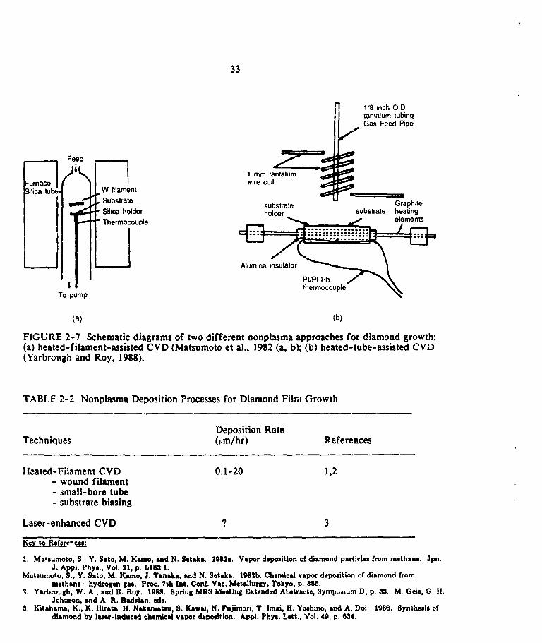
33
1/8 =nchO D.tantalum tubingGas Feed Pipe
;eed
_,,_ 1 mm tantalum
Furnace "_ wire coal
Silica tub W hlament
Substrate substrate Graphite
_[_ Sihca holder holder substrate heating
Thermocoupte _ _ j elements,/% -\1 ii
| Pt/Pt-Rh / _"_N
To pump thermocouplo %
(a) (b)
FIGURE 2-7 Schematic diagrams of two different nonp!asma approaches for diamond growth:(a) heated-filament-assisted CVD (Matsumoto et al., 1982 (a, b); (b) heated-tube-assisted CVD(Yarbrough and Roy, 1988).
TABLE 2-2 Nonplasma Deposition Processes for Diamond Filni Growth
Deposition RateTechniques (_m/hr) References
H¢ated-Filament CVD 0,1-20 1,2- wound filament- small-bore tube- substrate biasing
Laser-enhancedCVD ? 3
Key to References:
1. Matsumoto, S., Y. Sate, M. Ktmo, and N. $,taka. 1982s. Vapor deposition of diamond particles from methane. Jpn.J. Appi. Phys., Yol. 111,p, L183.1.
Mateumoto, S., Y. Sate, M. Kamo, J. Tanaka, mad N. Sataka. IN_b. Chemic al vapor deposition of diamond frommethane--hydrogen gN. Prec. 7th Int. Conf. Vac. Metallurgy, Tokyo, p. 386.
.'t. Yarbrough, W. A., and R. Roy. 1985. Spring MRS Meeting Extended Abstracto, Symp_=mm D, p. 33. M, Geis, G. H.Johnson, and A. EL.Badsian, ads.
3. Kitahama, K., K. Hirers, H. Nakamatsu, S. Kawal, N. Fujimorl, T. Imai, H. Yoahino, and A. DoS. 1986. Synthesis ofdiamond by Imr-lndueed chemical vapor depoeition. Appl. Phys. Left., Vol. 49, p. 654.
1990017647-047

34
__._nor-Liouid-Solid (VLS) Growth
The growth of diamond whiskers has been reported (Derjaguin et al., 1968), but nosignificant further work appears to have been done in the interven;ng 20 years. It was claimedthat the diamond whisker growth proceeded by the VLS process, but it is not known ho-_ theconditions differed from those used to grow graphite whiskers. In the latter case, iron beadsapproximately 100 to 200 A in diameter provide transport of carbon from the vapor to thegrowing tip of the whisker under conditions not too far removed from CVD diamond growth.Careful experiments are needed to determine what factors encourage diamond whisker growthand the possible role of hydrogen in the process.
Critical CVD Growth Parameters
Diamond crystals and films with the highest perfection have been grown by controlling thegas-phase chemistry. Although many of _he details of the fundamental nucleation and growthprocesses are 3till unknown (see later section), the critical deposition parameters of nucleation andgrowth have been explored extensively over the past several years. Interestingly, with fewexceptions, the critical parameters are similar for all of the various techniques described coveringa wide range of gas activation. Thus, unless noted, the general parameters apply to all of thesediamcnd deposition approaches.
Substrates and Their Preperation
Diamond has been nucleated and grown on a wide range of substrates, including metals,semiconductors, graphite, insulators, and even fused silica glass. Although the present evidenceis inconclusive, stable carbides at the diamond fiim-nondiamond substrate interface appear to beimportant. The origin of the carbide may be due to direct chemical reaction between theactivated gaseous species intentionally introduced into the system and the metal element in thesubstrate or to gas species originating from atomic hydrogen etching of the deposition reactorwal! or the substrate.
There is usually a delay time between the start of the deposition to the point whereindividual crystallites are seen and the time when they grow together to form a continuous film.The most effective methods for increasing the nucleation density and decreasing the delay timefor nucleation and growth have been to either scratch or seed the surface with diamond powderor add metal impurities (Si, Ti, B) in the gas phase. In the first case, the diamond crystalslittered on the substrate surface are, of course, excellent nucleation sites for immediate diamondgrowth. Epitaxial growth of diamond on diamond has been demonstrated by Spitsyn andcoworkers (1981L and Geis (1988). Other nondiamond powders (e.g., cubic BN, SiC, TaC) havebeen used to "seed"the surface (Bachmann et al., 1988).
Substrate Temperature
For the diamond films with the highest level of crystal perfection, the substratetemperature is usually in the range of 900 to 1000"C. This result seems to be independent ofdeposition technique (either PECVD or TECVD), and in all cases the film morphology consists ofapproximately 1- to 5-_,m-size crystallites in films about 5 j,m thick. The temperature obviouslylimits substrates to rather refractory materials.
1990017647-048
35
Diamond films with crystallite sizes of approximately 2000 A have been reported atsubstrate temperatures around 650"C while 100- to 200-A-size crystailites occur for substratetemperatures less than 600"C but greater than 450"C. The optimum temperature for crystalperfection is similar to that for the maximum in film growth rate.
Gases and Gas Composition
A large number of hydrocarbon gases have been used to deposit diamond. Although thereare no ,-eported significant differences in the resulting films, methane has been the gas of choice.In nearly all reported cases, large hydrogen gas dilution (e.g., about 1 percent CH, in H2) isnecessary with a trade-off between high rates (at about 5 percent CH,) and crystal size andperfection (at about 0.2 to 0.5 percent CH,). Recently diamond films of apparent comparablequality have been grown from CO. For CO, dilution with hydrogen appears radically different.Good-quality diamond films are obtained at 50 percent CO concentrations and even greater.
Gas Flow Rate and Pressure
The largest diamond crystals are obtained at pressures from 20 to 100 torr in both theplasma-assisted and thermally-assisted processes. In the case of PECVD, at law gas pressures,SiC formation increases while the plasma starts to become unstable at pressures above 100 torr.In the optimum range (especially at 50 to 100 torr) the plasma volume is small enough so it is notin contact with the reactor tube wall (typically 38- to 50-ram-diameter tubes for MPECVD).The film quality and deposition rate are relatively insensitive to the flow rate, which is typically50 to 1000 sccm.
Additions to Gas
Very little systematic work has been reported on either inert or reactive gas additions tothe Hz-hydrocarbon gas mixtures. More work is clearly nee&tlJ.
Position of Substrate
In all reports on PECVD diamond the substrates are immersed in the plasma or separatedonly by the dark space sheath in dc and rf plasmas. Remote plasma deposition in MPECVD hasnot been reported as yet, but the possibility cannot be discounted. For thermally assistedprocesses the substrate generally is placed aoout ! cm from the heated filament (or tube orthermal plasma nozzle). Remote deposition at distances greater than several centimetet-s has notbeen reported. Whether this is related to the lifetime of active species (atomic hydrogen andhydrogen-containing radicals, ions, or molecules) is yet to be explored.
Parameters Specific to Individual Processes
In the case of heated-filament CVD the filament temperature Is typically 2000 to 2300"C.Although the gas flow over and near the filament should be critical, this has not been controlledto date. For thermal plasmas the results are sketchy, but gas temperatures of 3000 to 10,000 Kare reported. Although the high deposition rates and excellent quality are encouraging, theapparent lack of film reproducibility (N. Koshino, personal communication) may simply reflectthe lack of control of the process at present.
1990017647-049

36
Size of Substrates
To make diemond deposition commercially feasible, high deposition efficiencies areneeded. One approach is to deposit over large areas, and for many applications (e.g., opticalwindows, semiconductor wafers, large numbers of cutting tools) this is essential. For substratediameter greater than 5 in., uniform substrate heating at approximately 1000"C for optimumdiamond growth will become a major problem. Although microwave plasmas have the advantageof stability and efficiency of production of plasma species, the geometrical constraints ofcoupling microwave energy to a plasma .'olume are significant. However, work in this directionis ongoing in both the United States and Japan. The ability to scale up dc and rf depositionprocesses is easier than with microwave; they seem less restrictive and have been usedsuccessfully in the a-Si:H solar cell field, for example. Scaling up of the heated-filament CVDmethod is a matter of constructing an array of heated wires and tubes, with the main drawbackbeing the uniformity of deposition thickness and properties.
Electric and lt,tagnetic Field Effects
Biasing of tl- _trates during dc plasma deposition results in diamond formation whenpositively biased "..,, _n carbide formation when negatively biased. The mechanism is not known,_ot even whether it involves only electrons or both electrons and ions (positive and/or negative)_If high-resistivity diamond films are eventually made, then dc plasmas wil! not work due to spacecharge buildup. If a positive bias on the substrate is essential, then this could be a limitation.
For microwave plasmas the electron cyclotron resonance (ECR) condition (875 gauss) forene:gy coupiln8 has been used. At high pressures (>! torr) ECR does not occur due to gas phase_'oilisions, but 9o._it_veresu)ts have been claimed regarding the ability to increase the extent ofthe plasmasoas coscaleto ',urgersubstrat_s.At the lower pressures(<0.1 torr) where the ECRcondition is valid_d_tn_ondgrowth hasbeen reportedat low temperatures(650"C). This area ofresearchof high plasmadensity deservesfurther investigation.
To the extent that electric andmagnetic fields allow for the acceleration,deceleration,anddeflection of active plasmaspecies, tEeseprocesscontrolswill allow merging betweenchemistr', controlledand bombardment-controlledgrowth of diamond. It is expectedthat thisarea will prove to be scientifically and technologicallyimportant.
Fundamental Issues in CVD Processes
There have been few reported studiesthat directly addressthe fundamental issuesofnucleationand growth of vapor-depositeddiamondfilms and the resulting film's structuralandchemicaldefects. This _ection, therefore, dealsmore with speculationsand attemptsto identifycritical areasof research. As is to be expectedfor an emergingmaterial technology,knowledgeof how to deposit films far exceedsthe understandingof fundamental mechanismsand kinetics ofnucleationand growth.
Nucleation
Since diamond is a metastable solid, the issue of nucleation involves not only that ofdiamond b Jt also graphite and the hexagonal polytype of diamond, Ionsdaleite. Furthermore,planar defects associated with the ( 111) planes in diamond--stacking faults, twinning, andintroduction of planar graphite planes between the (111) planes of diamond--have all been
1990017647-050

37
observed (Badzian et al., 1988; Davis et al., J987). The free-energy differences of these carbonphases are relatively small, so that kinetic factors, size effects, surface reconstructions, etc.,during nucleation could easily be more important than thermodynamic factors.
The widely varying morphological forms reported (Matsumoto and Matsui, 1983) forvapor-deposited diamond--cube, cuboctahedra, twinned cuboctaheda, pseudo-icosahedra,decahedral, Wulff polyhedra--are not _.!i found in natural or HPHT synthetic diamond crystals.There appear to be, however, some similarities between HPHT and vapor-deposited diamond. Inboth instances, stable carbides may provide favorable centers for diamond nucleation andsubsequent growth. Whether this is a requirement for heterogeneous nucleation on nondiamondsubstrates remainv to be seen.
Badzian and DeVries (1988), and othershave reviewedthe chemicalkinetics mode]fordiamondvapor depositiondevelopedby Derjaguin and Fedoseev(1977) and Fedoseevandcoworkers (1984). They start from thermodynamic calculations that show that the equilibriumpressure of carbon vapor over a diamond is about 2 times higher than over graphite. In theabsence of other factors, graphite nucleation is more probable than diamond. The Russianscientists considered ways tc overcome this inclination. In this approach, which considerschemical kinetics in the context of classical nucleation theory, there are several key points. First,the presence of a diamond surface (e.g., autoepitaxy or diamond-seeded surface) increases theprobability of diamond nucleation. Second, there should be a small range of conditions overwhich the nucleation rate of diamond is greater than that of graphite, _lthough this is not welldefined (Figure 2-8). Third, H2 dilution decreases the growth rate of graphite more thandiamond. And fourth, atomic hydrogen etches graphite faster than diamond. Thus, the Russian'itetature concluded that a single-step process for making diamond was possible, as shown inFigure 2-9. In Figure 2-9 note that (a) in the case of CH4 pyrolysis at certain supersaturationconditions, the specific growth rate of diamond (Vd)is higher than that of graphite (_), but bothincrease together; (b) in tbe presence of H', etching of diamond is insignificant, but. the etchingof graphite is dorvinant4 and (c) for mixtures of CH4 and H" there are conditions of pressure andtemperature where growth of diamond is significant and graphite is etched. In this competition,graphite nucleation and growth will essentially cease or will be covered by the diamond phase(Badzian and DeVries, 1988).
Data on diamond deposition rate as a function of temperature (Derjaguin et al., 1968)show a maximum at about 1000"C (under a limited range of conditions), which is consistent withthis model.
Jd
r.
0 J v
X
FIGURE 2-8 Ratio of diamond to graphite nucleation velocity as a function of supersaturation x(arbitrary units) (Badzian and DeVries, 1988).
1990017647-051

38
A. Only CH 4 B. Only H ° C. CH 4 + H°Growth only Etching only Combined growth and etclling
v_, I_ d g g
FIGURE 2-9 Relative growth and etch ra_esof diamond and graphite in the presence of ahydrocarbon (CH4) and atomic hydrogen (Badzian and DeVrics, 1988).
Badzian and Devries (1988) extend this approach by considering surface reconstructionsand relaxations on the (111) surface of diamond, which are known to occur also in the 900 to1000"C range (Pate, 1986). Other phenomena and properties that critically depend ontemperature in this same range include adsorption and desorption of hydrogen, etch pitorientatiGn, coefficient of static friction with metals, and oxidation rate. Based on this set ofcircumstantial evidence as a whole, a nucleation model that requires a =ritic_,!temperature wassuggested.
Clearly, the nucleation stage in diamond growth poses the most important questions thatwill have to be answered before there is significant progress in solving practical problems of low-defect-density polycrystalline films, high purity, homoepitaxy, heteroepitaxy, and controlledmorphology. Yet the current models of nucleation are primarily speculative, with a minimalamount of conclusive results reported. There is still no real understanding of critical nucleus sizeand crystallographic orientation; effect of impurities; catalytic effects (if any); intermediate layers(e.g., distinct or graded, stable carbides, hydrogenated); defect generation, propagation, andelimination; and gas-pha_e nucleation.
At an even more basic level, we still do not know enough about the detailed surfacechemistry and crystallography in this ca,'bon-hydrogen system to know whether diamond growthis the thermodynamically unexpected or expected structure. It has been suggested recently(Machlin, 1988) that there is a thermodynamically stable region for diamond in the C-H systemand that the diamond could be the expected phase to nucleate and grow under certain low-pressure conditions.
Growth Mechaninms
Before understanding diamond nucleation and growth from a vapor, a mechanistic andchemica! kinetics model must be developed. The key to any model will, of course, be aknowledge of the species at the growing film surface. Derjaguin and Fedoseev (1977) first
1990017647-052
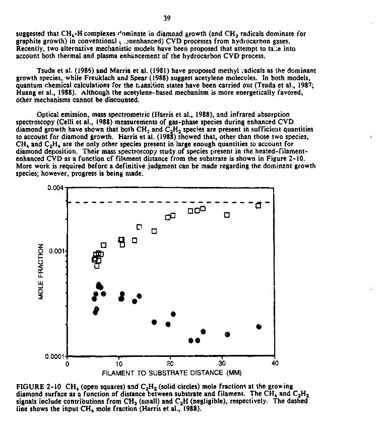
39
suggested that CH4.H complexes c%minate in diamond growth (and CH3 radicals dominate forgraphite growth) in convention_l _.3nenhanced) CVD processes from hydrocarbon gases.Recently, two alternstive mechanistic models have been proposed that attempt to ta'_e intoaccount both thermal and plasma enhancement of the hydrocarbon CVD process.
Tsuda et al. (1986) and Marria et al. (19gl) have proposed methyl :adicals as the dominantgrowth species, while Freuklach and Spear (1988) suggest acetylene molecules. In both models,quantum chemical calculations for the bans:,tion states have been carried out (Tsuda et al., 1987,Huang et al., 1988). Although the acetylene-based mechanism is more energetically favored,other mechanisms cannot be discounted.
Optical emission, mass spectrometric (Harris et al., 1988), and infrared absorptionspectroscopy (Celli et al., 1988) measurements of gas-phase species during enhanced CVDdiamond growth have shown that both CHz and CzHz species are present in sufficient quantitiesto account for diamond growth. Harris et al. (1988) showed that, other than those two species,CH, and CzH4 are the only other species present in large enough quantities to account fordiamond deposition. Their mass spectro._copy study of species present in the heated-filament-enhanced CVD as a function cf filament distance from the s,Jbstrate is shown in Figure 2-I0.More work is required before a definitive judgment can be made regarding the dominant growthspecies; however, progress is being made.
0.004 ....
ooo -cP o
O0
goO_ 0.001I-0<n-1.1.LU
o ,,,o&o*O ,
• • Q• ®
Oe
0.0001 ", , ,0 10 20 30 40
FILAMENT TO SUBSTRATEDISTANCE (MM)
FIGURE 2-10 CH, (open squares) and C=Ha (solid circles) mole fraction_ at the growingdiamond surface as a function of distance between substrate and filament. The CH 4 and C=Hzsignals include contributions from CH 3 (small) and CzH (negligible), respectively. The dashedline shows the input CH4 mole fraction (Harris et al., 1988).
1990017647-053

4O
Someof the importantaspects of diamondfilm growth that remain essentially unansweredare:
• Species on the growing film surface.
• Role of atomic hydrogenon the different crystallographicfaces of diamond during
growth.
• Surface structureduring film growth.
• Catalytic processes, if any.
• Surface kinetics and surface diffusion.
• Ion, electron, and radical bombardmentduring film growth.
• Synergistic effects of surface chemistry and bombardment.
• Growth rates--e.g., rate-limiting process(es);effect of impurities.
Impurities
The current vapor=depositedmaterialsare extremely impure, especially by semiconductorstandards. Atomic hydrogen, which is a necessaryingredient in diamondfilm deposition, is ahighly reactive element. Since silicon subs¢ratesand fused silica reactortubes and bell jazs areoften used, silicon is a common impurity. Levels of 0.2 atomic percent silicor have beenreported (Badzian et al., 1988) for films with close to optimm_ characteristics. It is expected thatdeposition techniques that providesufficient H"at the growing film surface and minimize H"interactions with the substrateand containmentvessel will be developed for those applicationsrequiring low or controlled levels of impurities. At that point the puriw of the startinggases willbecome important.
The main nonmetallicimpurity is hydrogen, with the lowest levels reported (L_nford,1987) being 435 * 79 9pma. the only systematicmeasurementsreported (Hartnett, 1988) showthat there is _n inverse relationbetween [H] in film and the Hz concent,'ationemployed duringdeposition, with the lowest level (see above) prepared in a 0.5 percent Hz-CH4 gas mixture. Insome instances(Lanford, 1987), the [H] concentrationwas over 1 atomic percent, and yet thefilms still showed the diamond diffraction pattern.
Silicon impurities have been relatedto an 80-fold increase in nucleation rate and a 2 to 3times increase in growth rate(Badzianet al., 1988). However, tee Raman spectra indicate anassociated ircrease in the 1332 cm"xand a strong, narrowband luminescence peak near 6000cm"x. The origin of this luminescenceband is still not understood,although an increase in thesilicon content has been suggested to be related to the presenceof silicon in octahedralholes ofthe diamond lattice (Hartnett, 1988),
The elimination and then controlled addition of impurityatoms is expected to be animportantaspect in both the scientific understandinsand the technologicaldevelopment. Littleinformation has been reportedto date.
q
1990017647-054

41
Defects
Essentia!ly nothing is known about point defects in CVD diamond fiJms (vacancies,interstitials, voids, or substitutional elemeqts), either extrinsic or impurity-related. Theoreticaland high-.resolution TEM (Glass et al., 1988) studies are expected to help understanding.
Planar defects such as mierotwins, stackihg faults, and graphite inclusions have beenviewed by medium- and high-resolution TEM (Glass et al., 1988). However, their relation topreparation conditions, impurities, etc., is unknown. Other defects such as dislocations and grainboundaries have not been fully investigated.
Since defects are important to essentially all film properties, considerable emphasis willhave to be placed here. Nucleation and renu. leation are expected to be related to defects andimpurities. At present only a little is known about the most obvious defects associated withstacking faults.
Morphology
Although a wide range of te:hniques have been used to deposit diamond films, the filmmorphologies reported ar_ similar. Also, in all cases the most structurally perfect crys'ais occurover a narrow range of process parameters, as described earlier. The diamond crystals grow ascubes, octahedra, cuboctahedra, and single and multiple (! 11) twins and intergrow aspolycrystalline layers with morphologies ranging from well-defined facets to poorly definedrounded shapes, highly irregular forms, etc. The crystal facets in many of the diamond filmsshow layer-like growth as expected from surface diffusion to steps and re-entrants (Badzian etal., 1988) and appear similar to crystals grown rather fast under high supersaturation conditions.
One of the problems facing diamond thin films is the fact that, at the conditions forgrowth of the most structurally perfect crystals, the faceted top surface of a typical 5-,,m-thickfilm shows a distribution of facet sizes usually centered around 1 _o 2 _,m. Such films are highlyscattering, thus limiting optical applications as well as optical analysis techniques such asspectroscopic ellipsometry and IR and optical transmission. Rough films are also unsuitable formany tribological applications as well. There are two approaches to obtaining smooth films:essentially zero nucleation density (single-crystal films) and extremely high nucleation density(submicrometer grain-size films). For applications in which mechanical properties and depositionon a nondiamond substrate are important, the latter approach is better. However, associated withfine-grain-size diamond films appears to be an increasing percentage of nondiamond material, as
. indicated by their Raman spectra (see Chapter 3). Certainly, _s the morphological units getsmaller, the internal surface area (internal morphology) increases, and the volume of materialaffected by tEese surfacescan be a significant fraction of the total volume, especia!ly when thecrystallite size approaches 200 to 100 A.
To what extent this phase purity problem is important remains to be seen. Certainly theanswer for each application is expected to be different, and trade-offs will have to be made.Other properties expected to be related to morphology (both internal and external) are adhesion,internal stress, friction, chemical stability, interdiffusion, electrical conductivity, and thermalconductl vity.
A.n evolutionary growth model for diamond films is expected to be important as attemptsare mad,', to design and engineer films for specific applications. A complete description and,;nderstsnding will entail a number of the fundamental issues already discussed--nucleation,intermediate layers, renucleation, intergrowth of crystals, evolutionary selection, arid effects of
1990017647-055

42
!mpurities and defects. A knowledgeof how to control nucleationrate and density, and perhapsto vary the growth rate in a deliberate mannerduring the early growth stageor throughouttheprocess(e.g., continuouslygradedor periodically gradedto make multilayers), will be a desirablegoal in future studies.
Diamond film morphology (often referred to as microstructure) has at least five facets,namely, (a) growth cones, (b) grain size, (c) grain shape, (d) grain orientation, and (e) defects.Growth cones are a very common feature of many different types of deposition processes and, infact, are a common occurrence in deposition of some of the materials discussed in this report,e.g., SiC. Growth cones commonly affect a variety of properties, usually in a negative fashion.Being collections of grains of very limited misorientation, they can commonly lead to anisotropyof properties, i.e., different properties through the thickness than in the place of the coating.They typically exacerbate surface roughness and surface finishing and limit fra_,ture toughnessand, especially, strength due to their acting as pseudo-large grains, and their boundaries orfrequent locations for accumulation of impurities, as well as possible porosity entrapment. Bothof the latter factors, of course, can have other negative affects, e.g., on _hermal conductivity.
Grain size has a variety of effects that can be either good or bad. Hardness typicallydecreases with increasing grain size, even in quite hard materials, e.g., SiC and B4C. Wearresistance follows a similar trend, again as shown in such hard materials as SiC and B4C. It is notclear whether fracture toughness has any significant dependence on grain size in cubic nlaterials,but tensile and compressive strengths clearly do, again with larger grains giving lower strengths.Clearly, for some of the electronic semiconductor applications, grain sizes must be large enoughto give a single crystal region of sufficient size for the semiconductor junction to have its propereffects.
Final!y, grain size also plays a role in resultant surface finish. Larger grains tend to leadto rougher as-deposited surfaces and also often limit the quality of surface finishing that canresult from machining. Grain shape, in particular the issue of whether or not columnar grainsare formed, can also be important, since columnar grains may lead to lower transverse fracturetoughness, i.e., easier transverse cracking. On the other hand, columnar grains may lead toenhancedtransversethermalconductivity.
Defects ranging from point, line, and planar lattice defects to voids and impurity particlescan all play a role in a variety of properties ranging from electronic to thermal to mechanical.Generally, defects are detrimental to most of these properties; they can in some cases, however,be either neutral or beneficial (e.g., lattice defects can be beneficial to hardness.
Film morphologyhasalsobeen related to residualstressesin PVD fibers, although not in aquantitative ma3ner. Generally dense,fine-grain-size fibers are in a high s:ateof compressivestress,whereascoarsergrain fibers often are closerto a neutral stressstateor even slightlytensile. Suchstressesare, again, a very commonproblem in depositedcoating. Suchstressesarefrequently observedto be seriousproblemsin someof the materialsdiscussedin this report, e.g.,SiC. Another possibleimportant sourceof suchresidualstressesmay be stoichiometry variations,which might thus be lesssevere;n diamondcoatings,but certainly could continu_ to be a similarproblem in BN coatings. Su_,nstressesbecomeof increasingconcernand .,eriousnessasboth thethicknessas w_ll asthe lateral dimensionsof the coating increase. Hence, thesecan becomeanimportant issuein scaling-up for many applications.
1990017647-056
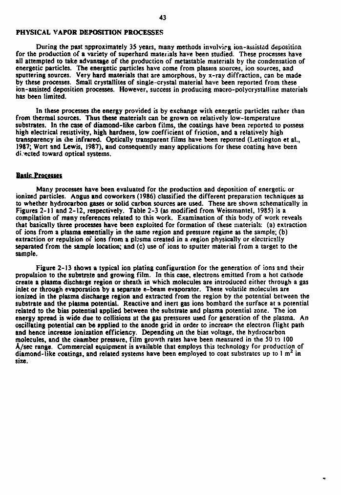
43
PHYSICAL VAPOR DEPOSITION PROCESSES
During the pq_st,'tpproximately 35 years, many methods involvirg ion-assisted depositionfor the production of a variety of superhard materials have been studied. These processes haveall attempted to take advantage of the production of metastable materials by the condensation ofenergetic particles. The energetic particles have come from plasma sources, ion sources, andsputtering sources. Very hard materials that are amorphous, by x-ray diffraction, can be madeby these processes. Small crystallites of single-crystal material have been reported from theseion-assisted deposition processes. However, success in producing macro-polycrystailine materialshas been limited.
In these processes the energy provided is by exchange with energetic particles rather thanfrom thermal sources. Thus these materials can be grown on relatively low-temperaturesubstrates. In the case of diamond-like carbon films, the coatings have been ,_eported to possesshigh electrical resistivity, high hardness, low coefficient of friction, and a relatively hightransparency in she infrared. Optically transparent films have been reported (Lettington et al.,1987; Wort and Lewis, 1987), and consequently many applications for these coating have beenall/acted toward optical systems.
Itaalg.P_r_ostnn
Many processes have been evaluated for the production and deposition of energetic orionized particles. Angus and coworkers (1986) classified the different preparation techniques asto whether hydrocarbon gases or solid carbon sources are used. These are shown schematically inFigures 2-11 and 2-12, respectively. Table 2-3 (as modified from Weissmantel, 1985) is acompilation of many references related to this work. Examination of this body of work revealsthat basically three processes have been exploited for formation of these materials: (a) extractionof ions from a plasma essentially in the same region and pressure regime as the sample; (b)extraction or repulsion of ions from a pbsma created in a region physically or electricallyseparated from the sample location; and (c) use of ions to sputter material from a target to thesample.
Figure 2-13 shows a typical ion plating configuration for the generation of ions and theirpropulsion to the substr_te and growing film. In this case, electrons emitted from a hot cathodecreate a plasma discharge region or sheath in which molecules are introduced either through a gasinlet or through evaporation by a separate e-beam evaporator. These volatile molecules areionized in the plasma discharge region and extracted from the region by the potential between thesubstrate and the plasma potential. Reactive and inert gas ions bombard the surface at a potentialrelated to the bias potential applied between the substrate and plasma potential zone. The ionenergy spread is wide due to collisions at the gas pressures used for generation of the plasma. Anoscillating potential can be _pplied to the anode grid in order to increase the electron flight pathand hence increase ionization efficiency. Depending on the bias voltage, the hydrocarbonmolecules, and the chamber pressure, film growth rates have been measured in the 50 to 100A/see range. Commercial equipment is available that employs this technology for production ofdiamond-like coatings, and related systems have been employed to coat substrates up to I mz insize.
1990017647-057

44
a. RF parallelplate b. RF _nduct=vedischarge C DC glow d=scharge
BIAS
'_ d. DC glow discharge e. Triode f. Hot fllamen!d=scharg_w=thbiasedscreen
•_.L __. SUBSTRATE
II
g. Hot filamen!discharge h. Pulsedd_schargetadgunwithauxd0ary_onbeam
FIGURE 2-11 Processesfor growing carbon films from hydrocarbon gases(Angus et al., 1986).
SUBSTRATE Q:_ I SUBSTRATE
CARBONTARGET TARGE'"
a. Dual beam sputtering b. Singlebeam sputtering
SUBSTRATE I !'o_ SUBSTRATE
LASER ,_1C_/_ o,_ Ar I;;Ar I_
_ Ar
"°o C q ICARBONI I" LCARBO CATHODE ",.--,------" " uTARGET BIAS
c. Laserevapora0onwith d. DC glowdischargewithauxiliaryionbeam acceleratinggrids
ANODECARBON CARBON RING SUBSTRATE
_.__._1 RODES CATHODE
,_ BSTRATE _ BIAS
e. Pulseddischargerail gun f. Vacuumarc.dischargerunsoff cathodematerial
FIGURE 2-12 Processes for growing carbon films using solid carbon (Angus et ai., 1986).
1990017647-058

45
TABLE 2-3 Decomposition Data for DLC, BN, and Related Composites
Appr_x_.-mte
Deposition Ion Energy (eV)
Pressure or Sample
;e¢_lque Reactants _Torr_ Bias Comments ReSonances
_Pla_l C2M 2 i0-3-i0 -4 G]_ssy ftJms 1,2l_lamitirm
C2Hh,(Ar) 1.2xi0 -2 2000-5000 V Black hard films 3-5
C2M 2 0.9 300- 400 V Yellow or bro_ inert films 6,7
RFPI_..,- C4HI0,(CH4.C3H 8) 0 2 i00-1900 V f:ard Insulatln8 films, 8-14D_Im_it_om depending on parameters
CzH Z 0.5 Yellow-brownlsh insulating 15filam
CZB6,(C2H2,C2H4,C3H 8) ?xl0 "2 500-I000 V Hard _ns_lat_ng films, p = 1.9- 16-182.0 g/cm
C2H 4 7xi0 -3 10-1400 V Very Low friction coefficients 19,20
C3!18 .15 400- 700 V Optical coatings 21
C6H C 2.2x10 -2 400-1800 V Optical and protective coa_i*_da 22,23
CH4,C2B 6 7x10 -3 500-2000 V Coatings with dismgnd-like 24,25propert_a_
CH 4 3x10 "2 540 V Investigations on k_netics and 26,27structure
CH4,C2H2,C2B 4 "×10 -2 Particle con$1omerates or films 28containing mlcrocrystals
C3Hg(Ar) - GeC interlayer to improve 29adhesion
7.5xi0 "6 10-1400 V Study of trlbology properties 30
_la_Zez C,(Ar,Kr) 1 5xl0 -4 Ion-beam sputtering 31-36
Dq_mlti_
C,B2.(Ar) .4 Ion-beam sputter_n_ wlth H+ 37,38
partlclpatlon
C,CH4,(Ar) 1 5x10 -4 200-i000 eV Dual-_on-be_n s_utterin_ 33,38-43
C,(Ar) 4 5xl0 -3 0- 300 V RF bi_s sputtering 44
C,C2H2,(Ar) ixl0 -3 Hybrid process: dc magnatron 45-50
sputterlnK and plasma
dec,xnpusitlon
C,C4HI0 3.7xi0 "2 0- 100 V Hybrid process, low-stress 51films
Ar 3 x10⁻² 150 V Ion beam sputter with assist 5Z
be_
Ar 7.5xi0-3 Magne_ron sputter at various $3
power levels
Ar 7 5xi0"3 O- 150 V Unbalancud magnetron with bias 54
Fxbrous carbon source 55
X,'_ C6H 6 (Tet*:altne, 2.2xi0 -4 20-5000 V Deposition rates of 30-I00 8,38,56-58P_ antrhacene) nm/mxn st tow pressures
Teeknlqmm
C6B6,AI,SI,Ti,Cr 2.2xi0 -2 200-3000 V Preparation of Melt-cOmpOsltea 38,59-64
C,CH4, (AE) 3000-5000 V Columnar fxlm morphology
I-m Beam C,(AI) 3.7xi0 -5 20- I00 eV Very hard, inert, transparent 9,65-70
Dalamiti rm films
C,CH4 - 900 eV Epitaxial layers on diamond
CB4 7.5x10 "2 20- 800 V Hard film_ containing micro- 71crystals
-9C,(Az) 5 x i0 30- I00 eV Mass filtered ton beam, small 72
crystallltes
C,(Ar) 7 x 10 -7 10-1000 eV Mass filtered ton beam, high 73
resxstlvity coatingsCO 5 x 10 -10 _- 300 eV Mess filtered ion beam 74
CH4{Ar) 2 x 10⁻⁴ i00 eV Dual ton beam deposlt:.on 75
CH4(Ar) 5 x i0"5 90- 2bO eV Single beam direct deposition 76
1990017647-059

46
TABLE 2-3 Decomposition Data for DLC, BN, and Related Composites (Continued)
Al_Proximats
Deposition Ion Energy (eV)Pxsasu_e or Sample
Tsc_mlqus React_ts (To_r _ bias Comments Raferonce_
Other C,(Ar) - 0- gs0 eV Laser evaporation with xon 34,77T_qaes bombardment
CH4 0.37 PuLsed plasma process 78C,(At) 750 Ion 5eneration from rlmdomly 79
muvin8 arc spot, high depos-ition rates
C(Ar) 1 x i0-5 Coaxial carbon plasma Sum 80
I)e1_oaitiom 8N.N2.(A_) 7.5110-3 RF sputtering, stoichio_tric 81,82of i-_ films
8N,N2,(Ar) 4.5110-3 0- i00 V RF bias sputterln$, inert, 83dense films
8,N2,NH3,(Ar) 1.5x10"3 0-3500 V Ion plating combined with 21,32,38,56,electron beam evaporation 60
BH3,E2H6,N2,N_3 - PLasma decomposition 84-8683,N3,H6,(Ar) 2.2xi0"4 200-1000 V Plasma decomposition 32,56,87B,N2 7.5110"6 40 keV Electron beam evaporation of B 88,89
with nltrosen ion bombardm0nt
B,N2 5 x 10⁻⁷ 2- 25 kV Boron E-beam evaporated, 90nitroBen ions
D3N3H5 5 x 10⁻⁴ Stoichiometric BN 91EN.Ar - FAB dual beam sputter 92
deposition
Raviw - - Review of UK RSRE applxcatLons 93A_Aclu
- A review of recent work on hard 94DLC films
- - DLC for thin film media for 95maSherS c rocordLnK
l(ey to References:
1. Schmellenmeir, H. 1963. Exp. Tach. Phys., Vol. 1, p. 49.2. Schmdlanmeir, H. 1955-$6. Z. Phys. Chem., Vol. 205, p. 349.3. Whitmell, D. S., and R. Willisun_n. 1976. Thin Solid Films, Vol. 3S, p. 255.4. Pick*fins, M., N. R. S. Tait, and D. W. L. Tolfr_. 1980. Depoeition and characteristics of ion plated carbon eostinp. Philoe.
Mat., Vol. A42, p. 257.5. Tsit, N. R. S., and D. W. L. Tolfr,_. 1981. Phys. Status Solid, Vol. A69, p. 339.6. Meyerson, B., and F. W. Smith. 19SOs. Electrical and optical prol_rties of hydropnatod amorphous carbon films. 3. Non-C_stal.
Solids, Vol. 35/_6, p. _4$.7. Meyerson, B., and F. W. Smith. 19S0b. Chemical modification of the elactricsl prol_rti_ of hydropnated smorphous carbon films.
Solid State Comm., Vol. 34, p. $SI.8. Holland, L., and S. M. Ojh*. 1979. The zrowth of carbon films with random •tomic structure from ion impact dsmN_ in •
hydrocarbon plums. Thin Solid Films, Voi. 58, p. 10T.9. Holland, L., and S. M. Ojhs,. 1976. Deposition of hswd and insulst!nz carbonsceous films on an KF taqjet in • butane plum•.
Thin Solid Films, Vol, 38, p. L17.10. Holland, L., and S. M. Ojh•. 1978. Infrared tr•n0pmnt and amorphous carbon ITown under ion imp_t in • butane plum•. Thin
Solid Films, Vol. 48, p. L21.11. Holland, L. 1980. A review of pl_m, procmm etudi_. Surface. Tachnol., Vol. 11, p. 146.12. Ojh,, S, M., end L. Holland. 1_77. Proc. Int. Vac. Consr., 7th, Vienna, 1977, p. 1667.13. Ojha, S. M., H. Nomtrom, and D. McCult.uch. 1979. The I_rowth kinetics and proparti_ of hard and insulatlnz carbonaceous films
grown in an RF disch,_. Thin Solid Films VoL 60, p. _lS.
1990017647-060
47
14. Vote, H., and R. J. Morlvec. 1981. Structural investigation of thin filrnJ of diamondlike carbon. J. Appl. Phys., Vol. 52, p. 61S1.15. Anderson, D.A. 1977. The electrical and optical properties of amorphous carbon preapred by the Glow discharge t_chnique.
Philos. Mq., Vol. 35, p. _.T.16. Andenmen, L.P. 1981. A review of recent work on hard I-C films. Thin Solid Films, Vol. S6, p. 183.IT. Andenmon, L. P., and S. BerE. 1978. Initial etching in an rf butane plMrna. Vacuum, Vol. 28, p. 449.18. Andenmon, L. P., S. Berg, H. Noretrom, and S. Towta. 1979. Properties and coating rat_, of diamond-like carbon films produced
by FR glow di_:harp of hydrocarbon g_. Thin Solid Films, Vol. 63, p. 165.19. Enke, K. 1981. Thin Solid Films, Vol. 80, p. 22T.20. Gsmbino, R. J., and J. A. Thompson. 1980. Spin resonance spectro_opy of amorphous carbon filnm. Solid State Commun.,
Vol. 34, p. 15.21. Beale, H.A. 1979. Cubic boron n:.tride. Ind. Res./Dev. (June), p. 143.22. Bubenzer, A., B. Diechler, and _.. Nyaieh. 1982. Optical properties of hydrogenated hard carbon thin films. Thin Solid Films,
Vol. 91, p. $I.23. Dischler, B., A. BubenNr, and P. Koidl. 1983. Hard carbon coatings with low optical absorption. Appl. P_,ys. Lett., Vol. 42,
p. 656.24. Fujlmori, N., A. Doi, and T. Yoshioka. 1953. Proc. Conf. Japan Society of Applied Physics, S0th, Tokyo, p. 214.25. Doi, A., N. Fujimori, T. Yoehioka, and Y. Doi. 1985. Plums deposition of crystalline carbon r,nd 1-Carbon film. Proc. Int. Ion
Eng. Cong., Kyoto, 1983 IEEJ, Tokyo, p. I137.26. Njalesh and Nowsk, 198.5.27. Hmdzimoto, K., T. Sakamoto, N. Matuda, S. Babe, and A. Kinbara. 1985. Physical proeprties of carbon films produced by plesma
CVD. Proc. Int. Ion Eng. ConE., Kyoto, IEEJ, Tokyo, p. 1126.28. H-% Z., S. Miturt, and B. Wendler. 1983. rf-plesma deposition of thin diamond-lie carbon film. Proc. Int. Ion Eng. Cong.,
Kyoto, 1983 IEP.J, Tokyo, p. 1143.29. Lettington, A. H. 1987. v_esEditions de Physique Paris, Vol. XVII._0. Gautberin, G., and C. Waiesmantel. 1978. Some trends in preparing film structures by ion beam methods. Thin Solid Films,
Vol. 60, p. 155.31. Weiesmantel, C. 1981. Ion beam deposition of special film structures. J. Vac. Sci. Technol., Vol. 18, p. 179.32. Pretum, J. 1984. Thesis, Techniecbe Hochschule, KarI-Marx-Stedt, German Democratic Republic.33. leujimori, S., T. Kesai, sad T. Jnamurs. 1982. C_.rbonfilm formation by laser evaporation and ion beam sputtering. Thin Solid
Films, Vol. 92, p. TI.34. Mathine, D., R. O. Dillon, A. A. Khan, G. Bu-Abbud, J. A. Woollarn, D. C. Liu, B. Banks, and S. Domits. 1984. Optical, Raman,
and pho_oemiesion results on amorphous "oiamondlike" carbon films. J. Vac. Sci. Technol., Vol. A2, p. 365.$5. Strelniski. V. E., V. G. Padaika, and S. I. Vakula. 1078. Properties of the diamond-like carbon film produced by the condensation
of a plMma stream with an rf potential. Zh. Teck. Fig., Vol. 48, p. $77.36. Mackow0ki, J. M., M. Berton, P. Ganau, and Y. Toues. 1982. Vide, Vol. 212, p. 99.37. Weiesmantal, C., K. dewilogua, K. Breanar, D. Dietrich, U. lgbarsbach, H. I. Erler, B. Rau, and G. Reiese. 1982. Preparation r_d
properties of hard I-C and I-BN coatino. Thin Solid Films, Vol. 96, p. 31.38. Weiesmantel, C. 1977. Trends in thin film depositon methods. Proc. Int. Vac. Cong., 7th, Vienna, 1977, p. 1533.39. Weiesmantal, C. 1976. Ion beam utilisation for etching and film deposition. Vide, Vol. 183, p. 107.40. Weiesmsmtal, C., G. Raiese, H. J. Erler, F. Hanny, K. Bewilozua, U. Ebersbech, and C. Schurer. 1979a. Preparation of hard
coatings by ion beam methods. Thin Solid Films, Vol. 3, p. 316.41. Nikiforova, N. N., M. B. Guesva, and V. G. Babtev. 1982. Proc. USSR Conf. InterLctious Atomic Particles Solids, 6th, Minsk,
1982, p. 112.42. Banks, B. A., and S. K. Rutledge. 1982. Ion beam sputter-deposited diamondlike films. J. Vec. Sci. Technol., Vol. 21, p. 807.43. Sathyamoorthy, A., and W. Weisweilar. 1982. Studies of the sputter deposition of carbon, silicon and SiC films. Thin Solid Films,
Vol. ST, p. _.44. Harding, O. L., B. Window, D. K. McKensie, A. R. Collins, and C. M. Horwits. 1979. Cylindrical magnetron sputtering system for
coating solar selective surfaces onto ba;ches of tubes. J. Vac. $ci. Technol., Vol. 16, p. 2105.45. Harding, G.L. 1980. Absorptsmce and emittance of metal carbide selec_ivt surfeces sputter deposited onto glm tubes. Sol.
l_.nergy Mater., Vol. T, p. 101.46. Harding, G. L., $. Craig, and B. Window. 1982. Production and properties of sputtered thin films for solar selective absorbing
surfaces. Appl. Surf. Sci., Vol. 11/12, p. 315.47. Craig, S., and G. L. Harding. 1982. Structure, optical properties end decomposition kinetics of sputtered hy6rogenated carbon.
Thin Solid Piling, Vol. 97, p. 345.48. McKansle, D. K., and L, M. Briu_. 1981. Properties of hyd_genated carbon films produced by reactive magnetron sputterinl.
SoL Enerr/Mater., Vol. 6, p. 79.49. McKanale, R. C. McPhedran, N. Sawides, and L. C. Botton. 1983. Properties and structure of amorphous hydrogenated carbon
films. Philos. MNL, Vol. B48, p. $41.60. Zeles, J. 198.5. Low-st_u diamondlike carbon films. J. Vhc. Sci. Technol., Vol. A1, p. 305.61. Pellicori, S. IS,, C. M. Peterzon, amd T. P. Hanson. 1986. Transparent carbon films: comparison of properties between ion- and
plesma-depoeit_ procesmm, J. Vac. Sci. Technol., Vol. A4, No. 5, p. 2550.62. Savvldes, N., and B. Window. 1986. Diamondlike amorphous carbon films prepared by magnetron sputterinfJ of graphite. J. Vac.
Sci. Technol., Vol. AS, No. 6.63. Sawldes, N., and B. Window. 1986. Unbalanced magnetron ion-misted deposition and property modification of thin films.
J. Vsc. Sci. Tw.hnol., Vol. A4, No. 3.64. Pulker, H. K., and R. Stzffler. 1979. U.S. Patent 4,175,53&
1990017647-061

48
55. W,iumanLel, C., K. B_wilozua, D. Dietrich, H. J. Erler, H. J. Hinnebers, S. Kloec, W. Nowick, and G. Reisse. 1980a. Structureend properties of qu_,i-smorphous films prepsred by ion beam techniques. Thin Solid Films, Vol. 72, p. 19.
56. Weisanumtel, C., H. J. Erler, and G. R*isse. 19T_b. Ion beam teclmiquse for thin and thick film deposition. Surf. Sci., Vol. 86,p. 207.
57. Weimmantel, K. Bewilosua, H. J. _Hm', H. J. Hinneherz, 9. Klose, W. Nowick, end G. Rei_se. 1980b. p. 188. In Low Enerrj IonBeuns, i. H. Wilson and K. G. St,phens, ods. Institute of Physics Conf. Series 54, Institute of Physics, Bristol and London.
58. Weisementel, C., K. Breuer, end B. Winds. 1985. Hard films of unususl mlcr_tructure. Thin Solid Films, Vol. 100, p. 385.59. W_dsementel, C. 198Sa. Proc. Int. Vsc. Conzr., 9th, Madrid, 1985, p. 299.60. Bewilosun, K., E. Buziel, B. Rau, C. Sohurer, end C. Wei_mentel. 1980. Krist. und Tech., Vol. 15, p. 1205.61. Weiesmentel, C. 191Lqb. Ion-bMod prepsur-tion of semiconductor end herd msterisis films. Proc. Int. Ion Ens. Cons., Kyoto, IEF,J,
Tokyo, p. 13ST.62. Tesr, D. G., end M. Ssdsma. 19?T. The ion pistins of c_bon. Thin Solid Films, Vol. 45, p. 553.63. Ssdsma M. S. 198.q. Deposition end chsrscteriJtics of ion plated csrbon coatinl_. Proc. Int. Ion Eng. Cons., Kyoto, IEEJ, Tokyo,
p.l64. Ai,enbers, S., end R. W. Chsbot. 19TI. Ion-benin deposition of thin films of dismondlike carbon. J. Appl. Phys., Vol. (2, p. 2955.65. Spencer, E. 6., P. H. Sochmidt, D. J. JoT, end F. J. Senuslon,. 1976. lon-besm-depo*itod polycrystalline diamondlike films.
Appl. Phys. Leer., Vol. 39, p. lie.68. Ai_nberlL S. 1984. Properties and applicstions of dismondlike cturbon films. J. Vec. Sci. Technol., Vol. A2, p. 369.6_. Furuse, T., T. Suenki, S. MstmsnJoto, K. Nishids, end Y. Nennichi. 1978. Insulatins carbon tontine on (ALGA) se DH Iwtr facets.
Appl. Phys. Leer., Vol. S.q, p. SIT.68. Monsvec, T. J., end T. W. Orent. 1981. Electron spectroscopy of ion beam and hydrocarbon plasma sneratod diunondlike carbon
films. J. Vsc. Sci. T,chnol. Vol. 18, p. 2_.(59. Fntemen, J. H., W. Temple, D. Beenlend, end O. A. Osrd. 19T6. Ion beam studies. I. Teh retardation of ion beams to very low
enersies in an implantation accelerstor. Nucl. InJtrum. Methods, Vol. 135, p. 1.TO.More, T., end Y. Namba. 198& Hturddismondlike csrbon films deposited I:y ionised deposition of methane Z_- J. Vsc. Sci.
Technol., Vol. AI, p. 33.Tl. Chsikov,kii, E. F., V. M. Pusikov, end A. V. Semenou. 1981. SOy. Phys. Cryetmdlozr., Vol. 26, No. 1.T2. Ishikawa, J., Y. Tskeiri, K. O|sws, end T. TskN0. 198?. Tren,pmnt cturbon film prepared by mue-separated nesative-csrbon-
ion*bes,m deposition. Jpr. J. Appl. Phys., Vol. 61, No. ?, pp. 8509-3615.TS. Kesi, S., H. Keng, end J. W. ltsb0dsds. 1987. Chemically bonded dismondlik, carbon films from ion-beam depositon. Phys. Rev.
Letters, Vol. 59, No. 1.T4. Mirtich, M. I. 1981. Ion beam dspoeitod protective films. NASA Technical Memorandum 81722. NASA Lewis Reeslurch Ce,,ter.75. Nir, D., end M. )distich. 194145.Thin film Srowth rate effects for primary ion beam dspo, ited diamondlike carbon films. J. VIc. Sci.
Technol., Vol. A4, No. S.?6. Fujimori, N., end K. Neq_i. 1981. The effect of ion bombardment on csrbon films prepsred by Iseer evaporation. Jpn. J. Appl.
Phys., Vo|. _10,p. L164.7T. Sokolowski, M., and A. Sokol_wda. 1983. Electr'_ccharge influence on the met_table phue nucleation. J. Crystal Growth,
Vol. ST, p. 185.78. Dorodnov, A.M. 19T8. Zh. Tekh. Fis., Voi. 9, p. 48.79. Sorer st. ILl.,1984.80. Airs, C. R., end N. C. Tren. 1983. J. Appl. Phys., Vol. 64, p. 6053.81. Wi810ns, M. D., C. R. Ait_, smc!F. S. Hickernell. 198& J. Vac. Sci. Technol., Vol. A2, p. $2_.8_. Roth, D., H. J. Erler, B. Rother, L. Richter, K. Peter, end B. Winds. 1984. Proc. Conf. Hochvakuum, Orensfiacben, Dunn*
Schichten, 9th Dresdsn, 1984. Vol. 1, p. 366, Phys. Soc. of GDR, Berlin,&q.Gafri, D., A. Grill, D. ltshlk, A. Inspektor, end It. Avni. 1980. Boron nitride coatinlp on steel and graphite produced with • low
pressure rf plums Thin Solid Films, Voi. 73, p. 63S.84. Miylunoto, H., M. HiroGe,end ¥. O,sk•. 1983. 9tructund end electronic ch,_rscteris•tion of dischlrse-produced boron nitride.
Jpn. J. Appl. Phys., Voi. 33, p. LII16.85. Sokolowdi, M., A. Sobolowd•, A. Michseiski, Z. Romenowski, A. Ru,ek-Muurek, end M. Wronikowski. 1981. Thin Solid Films,
Vol. 80, p. 5149.86. 9henfield, S., and R. Wolbon. 198,q. Ion beam synthesis of curbi boron nitrids. J. Vsc. Sci. Technol., Vol. AI, p. 323.ST. $stou, M., K. M•tude, end F. F_imoto. 1988. Proc. Symp. Ion Sources end Ion-Assisted Technology, 6th, Tokyo, 1982, p. 425.88. Sotou, M., end F. FuJimoto. 1983. Formstion of cubic boron nitride fllrm by boron evaporation and nitrogen ion beam
bombJurdment. Jpn. J. Appl. Phys., VoL |3, p. LI71.89. Andoh, K. O., Y. Susuki, E. Kendjo, M. Sotou, end F. F_imoto. 1987. Nuclear Instruments.90. Hslverson, W., end D. T. quints. 1986. Effects of chJurp neutrslieation on lon-besum-depoJitod bor:., nitrids films. J. Vsc. Sci.
Technol., VoL AS, No. 6.91. Shimoksw•, F., H. Kuweno, end K. Nt4sd. 1986. Proc. 9th Syrup- on ISIAT, Tokyo.9:. Lettins_on, A. H., _. C. Lewis, C. J. H. Wore, B. C. Monschen, end A. J. N. Hope. 1_87. Developments in GeC _s a Dureble
Coatins Str_bours, June 198T.98. TesS, H., end D. B. Bozy. 1987. Chsrsctertsstlon of disumondlike c_bon films end their applicatio, _ ..... cc,,ts cn thin-film
media for msgnetic recoedins. J. Vsc. 8ci. Technol., Voi. AS, No. (5.94. Ansus, J. C., end C. Hnymen. 1988. Low-pnmsure, metutsble growth of dien_ond an_ ",_,mondlike" phases. Science, Vol. _14, no.
_84_8,pp. 915-931.96. An8us, J. C., P. Koidl, end 9. Domits. 1986. Csrbon thin films. Chzpter 4 i, _luma Depositio_ _f Thin Films. J. Mort and
F. JenJen, eds. Boca R•ton, Florida: CRC Preu.
1990017647-062

49
_._._ Substrate
I - _ Growingfilm
' ; _ _ j Plasma sheath_ _ _, Screen
/ Hot cathode
U. UaU_ _. j Gas inlet
I Electronbeamevaporator
• Electrons]0 Ions
FIGURE 2-13 Ion plating configuration.
An alternative appr(ach to the ion plating techniqueis the useof an rf-plasma-assistedCVD systemalso usinga voltagebiason the sampleholder. A typical configuration is showninFigure 2-14. Radio frequency energyof 13.56 MHz is applied to the lower electrode. Thiscreatesa plasmabetweenthe lower electrodea_,l upper electrode that is at rf ground potential.Superimposedon the ff potential is a negative bias, typically 300 to 1000 V. This resultsinbombardment of the lower electrode(holding the samples)by energeticspeciesextracted fromthe plasma. An alternative configurationof this sametechnologyallows the sampleelectrodetoself-bias due to the very different inabilities of electronsand ions. This will alsoresult inenergeticbombardmentof the samples.
This configuration hasseensignificantdevelopmentfor the productio, of optical coatings.One applicationhasbeen for the depositionof hard a-C:H coatingson germaniumsubstrates.Equipment hasbeenconstructedfor coatingobjectsup to 1 m in diameter.
Figure 2-15 showsthe original sacrificial cathode ion sourcedevelopedfor direct ion beamdepositionof diamond-like carl_n coatings. In this I_rocess,a high-voltage dischargeis initiatedbetweenthe carbon cathodeand carbon anode in the ion source. Argon is suppliedto thisdischarge,and the resultingchargedargonions spotter the negative electrode, introducingsputteredcarbon into the plasmadischarge. Ions of argonand carbonare extracted throughanorifice by appropriate electronicextractioz_opticsand are impingedon the sampleheld in asecondvacuumchamberat substantiallylower pressure. This techniqueresults in amorphouscarbon coatingswith little or no hydrogen. In addition, the low vacuumpressureof thedepositionchamberresultsin a more uniform ion ev,ergy profile. Smallcrystallites (up to 5 #m)of diamondhavealso beenproducedby this technique.
1990017647-063

50
HydrocarbonGas Inlet
10"3Torr - 600 v
-tH,'
C', H', _ - Plasma
m I--'_'1 m
I Lower Electrode(Cu) I[ r"_
Vacuum IPump -_
.
FIGURE 2-14 rf plasmaconfiguration.
FIGURE 2-]5 Direct ion beamdepositionfrom solid precursorconfiguration.
1990017647-064

51
Another manifestation of the single ion beam direct-deposition approach is shown inFigure 2-16. In this technique, a standard Kaufman-type ion source is employed for thegeneration of energetic carbon and argon ions. Because a hydrocarbon feed is used, substantialquantities (up to 30 atomic percent) of hydrogen are incorporated into the resulting amorphouscoating. This inclusion of hydrogen can be beneficial in tailoring the refractive index of theresulting material. In addition to diamond-like carbon, this technique has also been employed forthe production of cubic BN coatings.
MAGNETCOIL
ANODE _ CHARGENEUTRALIZER SUBSTRATE
DISCHARGE FILAMENT HOLDER
CHAMBER oet_oOe,,,Oe,eO_ _ leo • O
cP°°°CATHODE O • oO I¢,10 • O • o e_
FILAMENT ¢_ ' OO'L,,=vO O•Oo •OO /: ELECTRONSIONS
8oN,Me , , -eoO . ,v /
VAPOR ', Z%:tt. g °° "°.°IONEXTRACTION
GRID
v,
FIGURE 2-16 Direct ion beam deposition from gaseous precursor configuration (Holland andOjba, 1978; and Berg and Anderson, 1979).
Figure 2-17 shows a modification of the single direct ion beam deposition configuration.In this technique, originally developed by workers at NASA's Lewis Research Center (Mirtich,1981) and other laboratories,a secondion sourceis typically operatedat higher ion energy thanthe depositing source. The resulting films have been shown to be clearer than diamond-like fi!msproduced from a single beam ion source using volatile precursor molecules.
Another modification of the dual ion beam system is shown in Figure 2-18. In this system,carbon is sputtered from a 8r_-phite target by the first ion source. The sputtered carbon isallowed to deposit on the substrate with or without secondary ion bombardment. A s£cond ionsource, operated at a lower ion energy, can be employed to further bombard the sample surface.This results again in films with improved mechanical and optical properties. This technique hasalso been employed for the production of cubic BN films.
1990017647-065

52
,_ . 8 cm Ion Source
// ArgonIons
,;/--..._...
Like Film
Beam Mixture of Mel_ne and Argon
Cathode Neutrahzer
FIGURE 2-17 Dual ion beamdepcsitionconfiguration(Mirtich, 1981).
Substrate
Film formation
_4/,_" Electron gun
N ,//SI .Inert - _ r ion beam
"V_,__,:°:,_,tm,P'X. It• _n source
FIGURE 2-18 Ion beam sputteringwith ion beamassist configuration.
1990017647-066

i
53
(_rittcal Grgwth Parameters
Amorphous diamond-like carbon and -,Jbic BN thin films have been produced byion-assisted processes primarily through close control of ion energy. Many of the fundamentalprocesses involving the nucleation of these films, the critical role of the impinging ion energy,and the relative roles of deposition ions (i.e., CNn+) versus argon ions are sti!! not well understooddespite extensive study _-/er many years. However, it is abundantly clear that a new class ofmaterials with very interesting physical, electronic, and optical properties can be produced bythis technology. The following sections point out some of the _.onsiderations necessary inproducing these materials.
Substrates and Film Nucleation
Since it is possible to operate ion-assisted processes at temperatures below 100"C, a widevariety of substrates have been studied in the deposition of these amorphous thin films.Substrates tested include a wide variety of optical materials (CR 39 optical pi_,stic, polycarbonate,glass, quartz, sapphire); infrared-transmitting optical materials, including germa:lium, zincsulfide, and zinc selenide; a variety of hard substrates im 'uding normal steels, cool steels, andcemented carbide substrates; and a variety of electronic-grade materials. Although thin films canbe produced on this wide variety of substrates, the adhesion properties of the coatings and theirresistance to abrasion vary widely. Generally, sputtering of the substrate pric,r to deposition isemployed to improve adhesion properties. In addition, thin interlayers such as germanium onZnS have also been used to improve adhesion (Lettington et ai., 1987).
The processes involved in the initial nucleation of the coating vary, depending on thedeposition process. Generally, coatings produced by ion plating techniques and those producedby ion beam sputtering nucleate quite easily, and films grow rapidly thereafter. However, filmsproduced by direcl ion beam deposition show a significant influence of substrate type on initialcoating nucleation. Seeding techniques such as those discussed in the earlier section entitled"Substtates and Their Preparation" are not generally employed for these amorphous coatings.
Deposition Pressure
As can be seen from Table 2-3. at least two distinct regions of process pressure are used indepositing these coatings. Coatings produced by ion plating and related techniques, wherein thegas discharge is in the same pressure regime as the sample, employ chamber pressures in themillitorr region. Direct ion beam deposition techniques, on the other hand, utilize _ressures inthe submillitorr region. Because of this fundamental difference, coatings produced by ion platingtypically grow at faster rates but have I_oorer optical and electronic properties than thoseproduced by ion beam processes.
ion Energy Considerations
Perhaps the single most widely studied process parameter employed in producingion-assisted coatings is control of the energy of the incident energetic particles, rhese studieshave clearly shown that many of the resulting film properties can be directly related to thecontrol of particle energy, len plating and related techniques typically use sample bias voltagesof 500 to )500 V. Because of the relatively high gas pressures utilized in these processes, theactual energy of particles impacting the surface is considerably less. in addition, a wide spreadof particle energies can be expected in these techniques.
1990017647-067

54
Direct ion beam deposition pr_esses have focused on ion energies ranging from 50 to 150eV. Careful control of ion energy in high-vacuum system_ employing mass filtering of carbonions has been shown to produce crystalline diamond materials up to several microm .ers in size(Chaikovskii et al., 1981).
Size of Substrates
Process equipment for coating substrates up to 1 m in diameter has been constructed forion plating and related deposition systems. Until recently, the area coated by direct ion beamprocesses has been restricted by the unavailability of large-area ion beam source technology.Most of the experimental work has been conducted utilizing sources capable of covering areas~ 15 cm in diameter or smaller. Recently, however, commercial ion beam sources have becomeavailable up to 38 cm in diameter. In addition, ion sources up to 1.5 m in diameter have beenconstructed at the NASA Lewis Research Center. The availability of large-coverage-area ionsources will accelerate development of direct deposition of these materials.
Fpudamcntal Issues in PVD Processes
Ion-assisted PVD processes take advantage of the production of metas:.abl-, species by thecondensation of energetic particles. The energy contained in the condensing particle ix employedin preferentially rearranging the bonding structure on the material surface. Much of thefundamental chemistry and physics occurring on the surface is still not well understood.However, some issues are clearly important, and a variety of theories have beeq aOvanced toexplain the nature of these resulting unique materials.
Growth Met ._auisms
AS particles of varying energy impact on a solid surface, a number of basic processes canoccur, including recoil of the particle from the surface, ejection of mate-:.l from the surfacecaused by the impact (sputtering), sticking of the particle to the surface, also with resultingenei'gy transfer from the particle to the solid surface, and implantation of the particle into thesurface with resulting energy transfer. A variety and combination of these processes may well beoccurring in many of the deposition approaches used for making amorphous diamond-lit:e carbonand _ther hard materials.
in the case of the production of diamond-like carbon, it is important to understand whycarbon atoms are deposited in the tetrahedrally bonded (sp s) structures versus the non-sp s bondedcarbon structure. One theory proposed to explain this observed result is that of preferentialsputtering (Spencer et al., 1976). Under the conditions usod in the deposition of these coatings,an arriving energetic particle is most likely to either recoil from the surface, condense or. thesurface, or eject materia! from the surface. Studies done by Angus and coworkers (1986) and byMiyazawa and coworkers (1984) indicated that impinging energetic particlos may have sufficientenergy to preferentially sputter non-sp s bonded carbon materials. Consequent_;, over a giventime period the material remaining on the surface will contain a preferential ertrichm_°nt of spsstructures.
The second proposed cGncept for the stabilization of sos bonded structures involves thehigh transient temperabJres and pressures that appear in the intmedi_te vicinity _..fan impactingenergetic particle. Weissmantel (19Sl) proposed _hat transfon_ations into sp s slructures car. occurduring these short-lived pressure and temperature events. Although the correctness of ,h.s theory
1990017647-068
55
has been debated, it appears clear that the growth surface is undergoing energetic bombardmentof sufficient energy for a variety of transformations to occur.
It does appear that, what-.ver the detailed mechanism of formation, the final structure ofdiamond-like hydrocarbons is close to that predicted for completely constrained, random covalent
• networks.
Microstruclure
Diamond-like carbon films have beenshownto contain a variety of hydrogencontentsandrangeof atGmicstructures. The majority of the densef:.ms have beenfound by x-rayexaminationto be amorphous. Sometimessmall crystal! teshave been identified, particularly infihns producedby ion beamprocesses.Thesecrystalliteshavebeen identified as having bothgraphiteand diamondstructures.
OTHER DEPOSITION PROCESSES
It is interesting to speculate that if part of the diamond-making process involves thestabilization of the surface, whether it be in the equilibrium or metastable regions, then theremay be other ways of doing this. There are two claims in the category of synthesis in thepresence of a liquid phase under metastable conditions: (a) the report of overgrowths on diamondin a mc en salt in the presence of nickel (Patel and Cherian, 1981); and (b) the breakdown ofAI4C3 in the presence of a carbon halide in a molten salt (French and French, 1981, 1982). Thelatter definitely produced fine-grai,ied hard po,,,ders. Although there has been adequate time forthe use of such processes if they were indeed successful, there appears to have been noconsummation of what are obviously exciting results. These should be reexamined.
_nother regime for study is the C-H-O system in the pressure range up to about 20 kb.There is an apparent convergence in the 'iterature on the reality of carbon deposition from thissystem in rature in liquids essentially immiscible with silicates.
Yet another approach to making diamond (and other high-pressure phases) at atmosphericpressure is the solid (graphite)-solid (diamond) transformation process mediated by intense laserirradiation of a loose, free-falling powder. Fedoseev and coworkers (1983) were the first toreport successful experiments by this process using a CO2 laser, and recently Alam and cowo-kers(1988) have confirmed these results using both CO2 and Nd-YAG lasers. The current drawbacksto this approach are the low conversion efficiency of the transformation process and the fact thatpowder and not continuousfilms are produced.
OTHER SUPERHARD MATERIALS")3
Silicon cr,rbide is considered a superhard material in the cot, text of this report, it is aboutone-third _. hard as digmond and comparab!e to cubic BN. Cubic BN is about half the hardnessof diamond and is the second hardest material known. Corundum, a-SiC, is the hexagonal (6H)phase that normally forms; it has been produced commercially for many years by the Ache.sonprocess. Generally these crystals form dark platelets of low purity. High-purity transparent SiCis more difficult to obtain because of difficulty in purity .':ndstoichiometry control, but crystalsof i x . x 5 mm have been produced.
J ! q m
1990017647-069
56
There are a large number of hexagonal and rhombohedrai polytypes and only one cubic(3C) polytype, E-SiC. The p-phase has been produced by vapor deposition processes, andvarious I_rocedures have been developed for heteroepitaxial growth on large-area siliconesubstrates based on various buffer layers to satisfy the mismatch in lattice parameter and thermalexpansion coefficient. Thick layers have been successfully prepared by a number of workers(e.g., Nishino et al., 1980; Liaw and Davis, 1985).
Although high-purity heteroepitaxial films could be achieved, they still contain a highdefect density of microtwins, intrinsic stacking faults, and antiphase boundaries. Recent resultsfrom the North Carolina State University group (see extensive rev,;ew by Davis et al., 1988, whichalso discusses diamond films deposition) of the deposition on Acheson-type a-SiC [both Si (0001)and C (0001) faces] show that these defects could be essentially eliminated, with the onlyremaining defect being of the double-positioning-boundary (DPB) type. And even these DPBdefects could be eliminated by 3" off-axis tilting of the substrate. However, in this latter casethe resulting film is a-SiC and not E-SiC.
Silicon carbide films can be doped both n- and p-type, and this combined with its highthermal conductivity and electrical field breakdown strength, makes it ati excellent material forelectronic devices. The potential electronic and nonelectronic uses of this new high-purity andlow-defect density material are jost beginning to be cxplored.
REFERENCES
Alam, M., T. DebRoy, R.Roy, and E. Brevel. 1988. Hig,i-pressure phases of SiO/sub 2/made inair by Fedoseev-Derjaguin laser process. Appl. Phys. Lett., Vol. 52, no./g, p. 16870.
Bachmann, P., W. Drawe, D. Knight, R. Weimer, and R. Messier. 1988. Diamond and Diamond-like Materials Synthesis (Extended Abstr_.cts), p. 99. M. Gels, G. H. Johnson, and A. R.Badzian, eds., Materials Research Society.
Badzian, A. R. !988. Superhard material comparable in hardness to diamonds. Vol. 53, No. 25,P. 2495. Appi. Phys. Lett.
Badzian, A. R., and R. C. DeVries. 1988. Crystallization of diamond from the gas phase:I. Mat. Res. Bull., Vol. 23, no. 3, p. 385.
Badzian, A. R., T. Badzian, R. Roy, R. Messier, and K. E. Spear. 1988. Crystallization ofdiamond crystas and filsm by microwave assisted CVD: Part II. Mat. Res. Bull., Vol. 23,p. 531-548.
Berg, S., and L. P. Ande:3on. 1979. Thin Films, Vol. 58, pp. 117-120.
Celli, F. G., F. E. Pehrsson, H. T. Wang, and J. E. Butler. 1988. Infrared detection of gaseousspecies during the filament-assisted growth of diamond. Appl. Phys. Lett., Vol. 52,p. 2043.
• Davis, R. F., J. T. _la, G. Lucovsky, and K. J. Bachman. 1987. Growth, Characterization, andDevice Development in Monocrystailine Diamond Films. Annual Report to Office ofNaval Research (Contract N00011 86-K-0666, June 1987).
q a ' I
1990017647-070

57
Davis, R. F., Z. Sitar, B. E. Williams, H. S. Hong, H. J. Kim, J. W. Palmour, J. A. Edmond,J. Ryu, J. T. Glass, and C. H. Carter. 1988. Critical evaluation of the status of the areasfor future research regarding the wide band gap semiconductors diamond, gallium nitrideand silicon carbide. Mat. Sci. Eng., Vol. BI, p. 77.
Derjaguin, B. V., and D. V. Fec:oseev. 1977. Growth of Diamond and Graphite From the GasPhase (in Russian). Moscow:. Nauka.
Derjaguin, B. V., L. L. Bouilov, and B. V. Spitsyn. 1968. Archiwum Nauki o Materiatach,Vol. 7, p. 111.
Fedosee% D. V., V. L. Bukhovcts, I. G. Varshavskaya, A. V. Laurent ev, and B. V. Derjquin.1983. Transition of graphite into diamond in a solid phase under atmospheric pressure.Carbon, Vol. 21, p. 237.
Fedoseev, D. V., B. V. Derjaguin, Y. G. Varshavskaja, and A. C. Semienova Tjan-Shanskaja.1984. Crystallization of Diamond (in Russian). Moscow:. Nauka.
French, F. A., and D. A. French. 1981. Production of Uitrahard Particle__. U.S. Patent No.4,275,050 (filed ] 1/8/79, issued 6/23/81).
French, F. A., and D. A. French. 1982. Ultrahard Particles of Carbon Produced by RetctingMetal Carbide With Nonmetal Halide in Hot Melt System. U.S. Patent No. 4,352,787 (filed11/8/79, is.oued 10/5/82).
Freuklach, M., and K. E. Spear. 1988. Growth mechanism of vapor-deposited diamond. J. Mat.Res., Vol. 3, p. 133.
Geis, M. W., G. H. Johnson, and A. R. Badzian, eds. MRS Spring Meeting Extended .Abstracts,Symposium D, p. 115.
Glass, J. T., B. E. Williams, R. F. Davis, and K. Kobashi. 1988. Proceedings of the 1st Int. Conf.on the New Diamond Science and Technology, Tokyo, October 24-26, Paper 3-10, p. 165.
Harris, S. J., A. M. Weiner, and T. A. Perry. 1988. Measurement of stable sgecies vresent duringfilament_assisted diamond growth. Appl. Phys. Lett., Vol. 53, p. 1605.
Hartnett, T. 1988. Characterization of Diamond Deposition in a Microwave Plasma. M.S.Thesis, Pennsylvania State University.
Hirose, Y., and M. Mitsuizumi. 1988. New Diamond (in Japanese), Vol. 4, p.34.
Holland,L.,and Ojba,S.M. 1978.ThinSolidFilms,Vol.48,pp.21-21.
Huang, D., M. Freuklach, and M. Maroncel_i. 1988. J. Phys. Chem., Vol. 92, p. 6379.
Kamo, M. Y. _to, S. Matsumoto, and N. Setaka. 1983. Diamond synthesis from gas phase inmicrowave plasma. J. Cryst. Growth, Voi. 62, p. 642.
Koshino, N., K. Kurihara, M. Kawarada, and K. Sasaki. 1988. Diamond and Diamond!ikeMaterials (Extended Abstracts), p. 95. M. Gels, G. H. Johnson, and A. R. Badzian, eds.,Materials Research Society.
1990017647-071

58
Lanford, W. 1987. 2nd Annual Diamond Technology Initiative Meeting. Sponsored by theOffice of Naval Research and SDIO/IST, Durham, North Carolina, Paper 8-P-O.
Liaw, P. H., and R. F. Davis. 1985. Epitaxial growth and chfracterization of beta -SiC thinfilms. J. Electrochem. Soc., Vol. 132, p. 642.
Littleton, A. H., J. C. Lewis, C. J. H. Wort, B. C. Monachan, and A. J. N. Hope. 1987.Developments in GeC as a durable coating. Amorphous Hydrogenated Carbon Films, In E=MRS Meeting, Strasbourg, June.
Machlin, E.S. 1988. On the stabilization of diamond relative to graphite by surfaces.J. Mat. Res., Vol, 3, p. 958.
Matsumoto, S. 1985. Chemical vapour deposition of diamond in rf glow discharge. J. Mater.Sci.Lett.Vol.4,no.5,pp.600-602.
Matsumoto,S.,and Y. Matsui.1983.Electronmicroscopicobservationof diamondparticlesgrown from thevapourphase.J.Mat.Sci.,Vol.18,p.1785.V. K.:Chapman & Hall.
Mirtich,M.J. 1981.lonbeam depositedprotectivefilms.NASA TechnicalMemorandum8!722.NASA LewisResearchCenter.
Mishima,O.,J.Tanaka,S.Yamaoka,and O. Fukanaga.1987.High=temperaturecubicboronnitridep=n junctiondiodemade athighpressure.Science.Vol,238,p.181.
Miyazawa,T.,S.Misawa,S.Yoshida,and S.Gonda. 1984.Preparationandstructureofcarbonfilmdepositedby a mass=separatedCSUP(+)ionbeam. MaterialsDivision,ElectrotechnicalLaboratory.Japan.J.Appl.Phys.55(I),pp.188=193.
Nishino,S.,Y. Hazuki,H. Matsunami,and T.Tankaka. 1980.Chemicalvapordepositionofsinglecrystallinebeta=SiCfilmson siliconsubstratewithsputteredSiCintermediatelayer.J.Electrochem.Soc.,Vol.127,p.2674.
Pate,B.B. 1986.The diamondsurfaceatomicandelectronicstructure.SurfaceSci.,Vol.165,p.83.
Patel,A. R.,and K. A. Cherian.1981.Crystallizationofdiamondatatmosphericpressure.IndianJ.of Pureard AppliedPhy_.,Vol.19,pp.803=820.
Safer,D. M., D. A. Gulino,and S.K. Rutledge.1984.NASA Tech.Memo 83600.
Spitsyn,B.V.,L.L.Bouilov,and B.V. Derjaguin.1981.Vapor growthofdiamond on diamondand othersurfaces.J.Cryst.Growth,Vol.52,p.219.
Suzuki,K.,H. ¥asuda,and T. Inuzuka.1987.Growth ofdiamond thinfihnsby dc plasmachemicalvapordeposition.Appl.Phys.Lett.,Vol.50,no.12,p.728.
Tsuda,M,, M. Nakajima,and S.Oikawa. 1987.The importanceof thepositivelychargedsurfacefortheepitaxialgrowthofdiamondsatlow pressure.Jpn.J.Appl.Phys.,Vol.26,p.L527.
1990017647-072
59
Tsuda, M., M. Nakajima, and S. Oikawa. 1986. Epitaxial growth mechanism of diamond crystalin CH/sub 4/-Hsub 2/pluma. J. Am. Chem. Sot., Vol. i08, p. 5780.
Vickery, E. 1973. Process fer Epitaxial Growth of Diamonds. U.S. Patent 3, 714, 334.
Weissmantel, C. 1985. Preparation, Structure and Properties of Hard Coatings, in Thin filmsfrom Free Atoms and Particles. New York: Academic Press.
Wort, C. J. H., and J. C. Lewis. 1987. Erosion Resistant Coatings for Infra-red Windows in the8-14/am Band. In Electro-Optical Systems and Image Analysis for Airborne Applications.AGARD Avionics Panel Symposium, Athens, Greece, October 1987.
Yarbrough, W. A.o and R. Roy. 1988. Diamond and Diamondlike Materials (ExtendedAbstracts), p. 33. M. Geis, G. H. Johnson, and A. R. Badzian, eds., Materials ResearchSociety.
1990017647-073

3
CHARACTERIZATION TECHNIQUES RELEVANT TO SUPERHARD MATERIALS
Many different types of analytical techniques have been used to characterize thesuperhard materials. More traditional methods such as optical microscopy, optical absorption,x-ra) diffraction (XRD), x-ray fluorescence (XRF), and Auger spectroscopy, have proved veryusefu_ in ways that have been discussed at length in other publications (Field, 1979; Sze, 1983;Tsai and Bogy, 1987). The special characteristics of the superhard materials and their unusualgrowth methods, however, have led investigators to rely heavily on a number of less commonlyused techniques. This chapter provides background regarding the nature of these techniques andthe information they provide and points out the need for new characterization methods. Theareas covered include techniques for characterizing phases present, surface structure, chemicalcomposition, and properties such as thermal, electrical, and optical. The need for fundamentalstudies of the diamond-like materials is also discussed.
STRUCTURE STUDIES
Determination of the different carbon phases incorporated in diamond and diamond-likecarbon materials is of importance for controlling the growth or deposition conditions. Severaltechniques are sensRive to differences between carbon chases, including Auger electronspectroscopy, electron energy loss spectroscopy (EELS), and Raman spectroscopy (Soli_RandRamdas, 1970). Since Auger and EELS are surfac_ analysis techniques, they are sensitive only tothe first 3 nm of the surface and hence incapable of characterizing the bulk of the material.Raman spectroscopy appears to be the analytical tool of choice because the diamond Raman peakat 1332 em': is easily distinguished from peaks related to other forms of carbon, as shown inFigure 3-1. A detailed investigation of the Raman spectra of films prepared under variousdeposition conditions, correlated with Auger and EELS data, should lead to the development ofstandard reference materials for calibrating instrumentation in the Field (as opposed to theresearch laboratory).
In addition to the Raman signal, a photoluminescence signal may also be present. Thisfluorescence background arises generally from defect centers within the films and therefore couldprovide an analytical tool for their identification. This may be important for films to be used inelectronic or optoelectronie applications because free carrier properties sucb as carrier lifetimeand mobility may be affected by them. The presence of the fluorescence signal does introduce a
61
1990017647-074
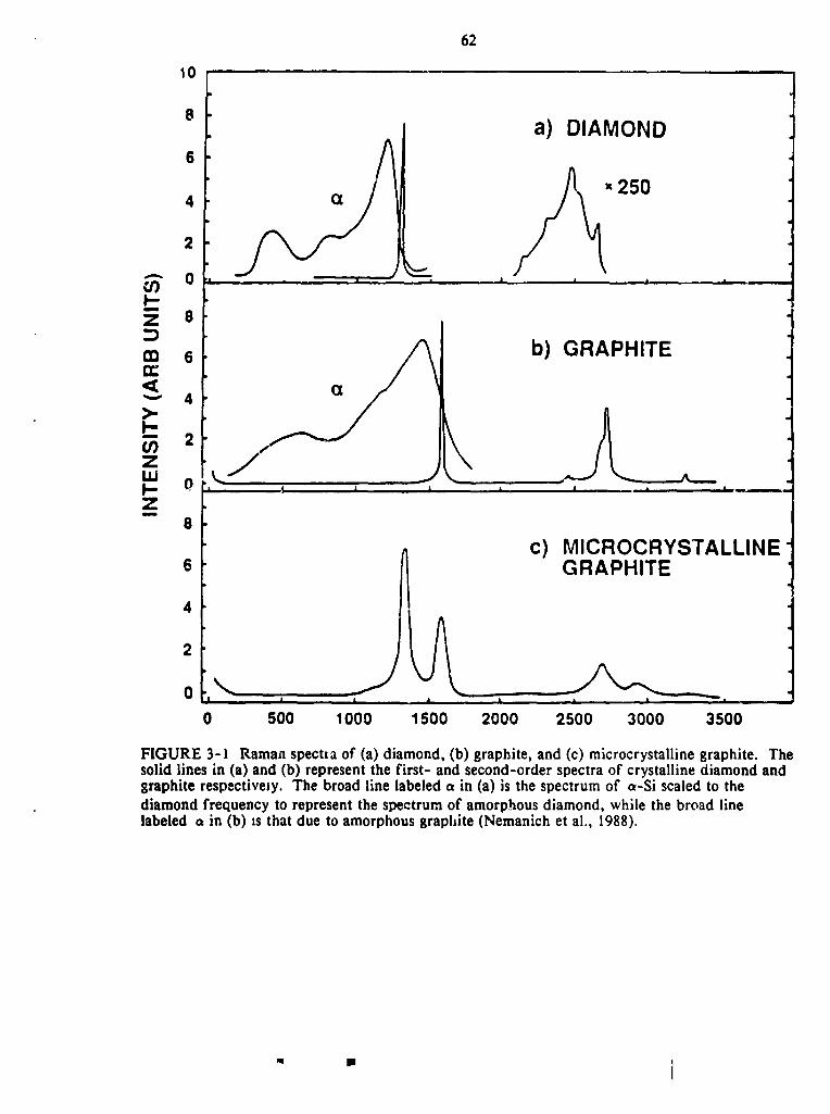
62
tO
o a) DIAMOND6
4 _x 250
2
i-ira=
Z 8
n-= 6 _ _ b) GRAPHITE
.¢4
>-I--
I-- 0 , _ I i _ , -, ,_,Z
0
c) MICROCRYSTALLINE6 GRAPHITE
4
2o ,"- J, i i i i =
0 500 1000 1500 2000 2500 3000 3500
FIGURE 3-1 Ramanspect=aof (a) diamond,(b) graphite,and(c) microcrystallinegraphite. Thesolidlinesin (a) and(b) representthefirst- andsecond-orderspectraor"crystallinediamondandsraphiterespectively.The broadlinelabeled_,in (a) isthespectrumot"<=-Siscaledto thediamondfrequencyto representthespectrumof'amorphousdiamond,whilethebroadlinelabeleda in (b) ssthatdue toamorphous8rapSite(Nemanichet el., 1988).
,, B i
1990017647-075

63
problem,however,sinceitrepresentsa backgroundsignalthatmustbe subtractedfrom theRaman signal. If the fluorescence signal is large, experimental uncertainties introduced in thesubtraction process could limit the ability to make the Raman data quantitative for thisapplication.
The most critical single parameter for understanding the nature of the diamond and DLCmaterials is the sp3/sp z ratio. Diamond is characterized by sp3 bonding between atoms, andgraphite is ct_aracterized by spa bonding. The sp3/sp2 ratio can be determined by severaltechniques, including nuclear magnetic resonance spectroscopy (Hoch and Reynhardt, 1988),elecU'on energ_ loss spectroscopy, and optical measurements of the dielectric function. Also ofgreat interest is the distribution of hydrogen over the different types of carbon sites (CH, CI-12,and CH3). This can be determined using Fourier transform infrared spectroscopy (FTIR). Thediamond-like materials are typically amorphous, and the local environment around each carbonatom may provide information of interest. This can presumably be accomplished by neutron orx-ray diffraction techniques. Extended x-ray absorption fine structure spectroscopy (EXAFS)may also be useful in this context. The concentration of dangling bonds (free radical sites) maybe measured by electron spin resonance (ESR).
The diamond-like materials often exhibit a medium-range order, which may be smallclusters or microcrystallites. High-resolution transmission electron microscopy will undoubtedlybe of value in characterizing these features.
_lf._ce Characterization
The surface s_ructnre of diamond is extremely stable and is responsible for some of itsinteresting properties (e.g., low coefficient of friction and negative electron affinity).Characterization techniques useful for examining the structure of diamond surfaces may beconveniently divided into three categories, depending on whether the_"measure geometricstructure, electronic structure, or chemical composition. A summary of these techniques follows.
Geometric Structure
The classical methods for studying the geometric structure of crystalline surface_ are low-energy electron diffraction (LEED) and high-energy electron diffraction (HEED). Thesemethods are well known and require no discussion here.
Grazing angle x-ray scattering can also be used to give information about geometricsurface structure. To apply this technique to monolayers, one requires a synchrotron x-raysource--e.g., the Brookhaven source--and very low scattering angles.
In recent years the scanning tunneling microscope (STM) has been developed. It is anextremely powerfui method that can resolve individual atoms on surfaces but cannot be appliedto insulating mater:4als. The scanning force microscope, on the other hand, does not require aconducting substrate; however, its resolution is significantly less than that of the STM. Theexpectations are that the scanning force microsco._e will be able to provide atom resolution withinthe next few years.
1990017647-076
64
Electronic Structure
The electronicstrvcture of adsorbed species on surface can be studied by angle resolvedphotoelectronspectroscopy. Either x-ray or ultraviolet photonscan be used. The angularandenergy distribution of emitted electrons gives direct information on the electronic structure of thesurface, from which geometric structurescan also be inferred. Auger spectroscopy may also beuseful.
Ultrahigh-vacuum ellipsometric spectroscopy can be used to investigate the electronicstructure of surfaces. It can provide a measure of the dielectric coefficient tensor and itsfrequency dependence at optical wavelengths. This provides information about surface electronicstates. In principle, the IR region can be done as well.
Chemical Composition
There are, of course, a number of other well-known surface analytical methods that giveinformation on the composition, and sometimes bonding, in the near-surface region. These aresecondary ion mass spectroscopy (SIMS), Auger spectrosco,_y, photoelectron spectroscopy andelectron spectroscopy for chemical analysis (ESCA). For highly insulating materials, secondaryneutral mass spectrosco.,y (SNMS) may be useful.
Dynnmic Processes
Inelastic scattering processesgive information on the motion of scatteritJgcenters. Bothinelastic neutronscattering and inelastic laser light scatteringcan be applied to the study ofdiamond surf_-ces. Molecularbeamscattering from diamond surfaces, perhaps using C*or H+,also might be considered. Scatteringintensity as a function of angle and energy will giveinformation aboutdynamic processeson the surface.
Fourier transform infraredspectroscopy is an extremely powerful method for analyzingthe vibrationalmodes of absorbedspecies. FTIR is now capableof monolayer sensitivity bymeansof double-reflection infraredand attenuatedtotal reflection techniques. Ramanspectroscopycan also be done in a Fouriertransformmocleand may prove useful for studyingnucleation processes.
High-resolution electron energy loss spectroscopycan also be used to obtain informationon the vibrationalstructureof absorbedspecies.
Molecular Modeling
Molecular modeling methodsare powerful tools for the study of surfaces. Both staticstructuralproblemsand dynamic processesmay be studied. For example, molecularmechanicsand more advanced ab initio quantummechanical techniquescan be used to study the state ofreconstructedcrystalline surfaces. Random, diffusive processeson surfaces can be modeled using
stochastic methodsdirectly--e.g., throughthe general Langevinequation for generating
trajectori,,sand variousMonte Carlo algorithms. Also, mol,,cular_dynamic techniquescan be usedto develop trajectories, from which dynamics can be studied. Supercomputersare required foradvanced wo_'kin either of these areas.
1990017647-077

65
ELEMENTAL COMPOSITION
It is astonishing that a majority of reports on the DLC and diamond materials still do notinclude a measurement of the elemental composition of the films. Of particular importance is theamount of hydrogen. Hydrogen can be conveniently determined by XSNnuclear reaction analysis(NRA), which provides a depth profile of hydrogen concentration. Hydrogen can also bedetermined b'_,helium forward scatter spectroscopy, but with a hi_her detection limit. Analysisof heavy elements is conveniently done by Rutherford backscatter spectroscopy (RBS). Augerspectroscopy is also useful for elemental analysis, and when combined with sputtering can givecomposition profiles as well. However, both RBS and Auger spectroscopy have detection limitson the order of 10"a atomic percent. When lower detection limits are required secondary ion massspectrvscopy or neutron activation is useful. Finally, combustion analysis can providemeasurements of hydrogen, carbon, oxygen, and nitrogen for samples of milligram size.
FUNDAMENTAL MECHANICAL MEASUREMENTS
Surprisingly few measurements of the fundamental mechanical properties of CVDdiamond and diamond-like materials have been made. Of particular interest would be themeasurements of the modulus of elasticity, the thermal expansion coefficient, the thermalconductivity, and the level of internal stress. All of these mechanical properties are offundamental importance for many proposed applications.
The films appear to be very impermeable; however, there are no accurate measurementsof the permeabilities of these materials. Applications of diamond and diamond-like materials asdiffusion barriers, corrosion protection layers, and vapor barriers will depend on thepermeabihties.
A simple and very instructive property that should be routinely measured is the massdensity. When combined with the knowledge of elemental composition, this permits placing thematerial of interest in the field of atom number density versus atom fraction hydrogen (Figure3-2). This type of plot provides a convenient way for categorizing different classes ofhydrocarbons and cgrbon. Similar compounds, for example the n-aikanes (AL), fall in tightgroupings ot the diagram. Diamond, DI, is at the upper left-hand corner. The adamantanes,AD, which are 10 and 14 carbon atom molecular diamonds, are at the lower right of thediamond-like hydrocarbon (a-C:H) grouping. The diamond-like hydrocarbons (filled symbols)range from approximately 0.20 to 0.60 atom fraction hydrogen and have number densities greaterthan 0.19 gram-atom per cubic centimeter. The vertical dastted lines show the theoreticalcomposition range predicted for fully constrained, random hydrocarbon networks. The atomnumber density of a-C-H increases with hydrogen content, in contrast to the behavior ofconventional hydrocarbons. This increase is caused by the increase in average coordinationnumber of carbon from 3 to 4 as the amount of hydrogen is increased. The diamond-likecarbons (a-C) appear to be a different class of material, with little or no hydrogen and with atomnumber densities from _,pproximately 0.19 to 0.28 gram-atom per cubic centimeter. These
densities indicate significant spa, tetrahedral, bonding. The amorphous carbons (AM) aredominated by sp, trigonal, bonding and can be formed by la_er or electron-beam evaporation.Other symbols are AC, oligomers of acetylene; AD, adamantanes; AR, polynuclear aromatics; andGR, graphite,
There are indications from several sources that the diamond-like materials areinhomogeneous, in particular, variations of elemental composition and properties with depth ofthe film are suspected. This question is rarely addressed but should be considered when assessingfilm properties. The interface between diamond or diamond-like materials and various substrates
|
1990017647-078
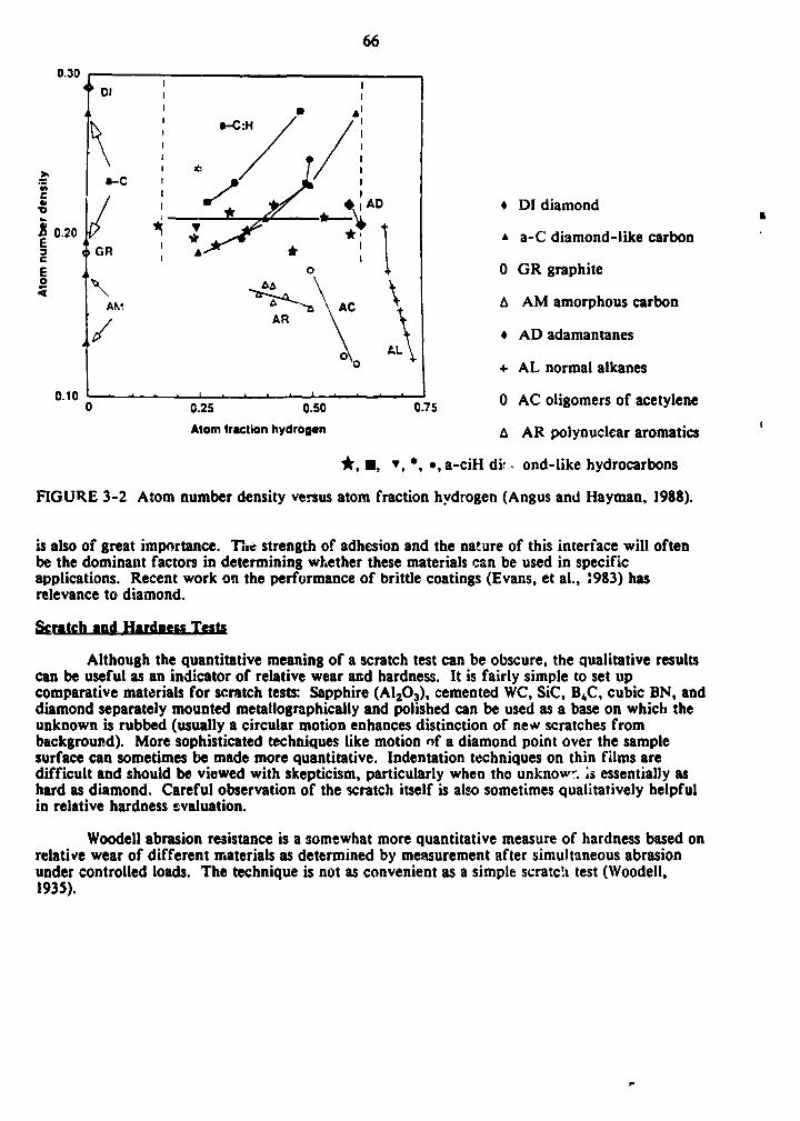
66
0.30 _, OI II• &l
•-- C
0.20 _ * a-C diamond-like carbonE GR iC I
E o O GR graphite
< A_: _"-_ AC _ _ AM amorphous carbont AD adamantanes
t.o + AL normal alkanes
I
o.10 L . . . , , , , ....... 0 AColigomersofacetylene0 0.25 0.50 0.75
Atom traction hydrogen /1 AR polynuclcar aromatics (
'Jr, II, v, *, s, a-ciH di:_ ond-like hydrocarbons
FIGURE 3-2 Atom number density versus atom fraction hydrogen (Angus and Hayman, 1988).
is also of great importance. TI,c strength of adhesion end the nature of this interface will oftenbe the dominant factors in determining wf,ether these materials can be used in specificapplications. Recent work on the performance of brittle coatings (Evans, et al., :983) hasrelevance to diamond.
Scratch and Hardness Tests
Although the quantitative meaning of a scratch test can be obscure, the qualitative resultscan be useful as an indicator of relative wear and hardness. It is fairly simple to set upcomparative materials for scratch tests: Sapphire (AI203) , cemented WC, SiC, B,C, cubic BN, anddiamond separately mounted metallographically and polished can be used as a base on which theunknown is rubbed (usually a circular motion enhances distinction of new scratches frombackground). More sophisticated techniques like motion nf a diamond point over the samplesurface can sometimes be made more quantitative. Indentation techniques on thin films aredifficult and should be viewed with skepticism, particularly when the unknowr, is essentially ashard as diamond. Careful observation of the scratch itself is also sometimes qualitatively helpfulin relative hardness fvaluation.
Woodeil abrasion resistance is a somewhat more quantitative measure of hardness based onrelative wear of different n',aterials as determined by measurement after simultaneous abrasionunder controlled loads. The technique is not as convenient as a simple scratc_ test (Woodell,1935).
1990017647-079

67
THERMAL CONDUCTIVITY
Many of the applications of superhard materials, especially CVD diamond, will relyheavily on their high thermal conductivities (Figure 3-3). Recent work has shown tha+ thethermal conductivity of CVD diamond depends strongly on the hydrogen/methane ratio used inthe microwave plasma CVD process and that the measurements correlate strongly with the DLC1332 cm "1 peak in the Raman spectrum (Ono et al., 1986). It has also been shown that thethe_tal conductivity of CVD diamond below room temperature is significantly lower than that ofnatural diamond crystals (Moreili et al., 1988), possibly because of the small crystallite si=es inCVD Jiamond. This variability makes it imperative that the thermal properties of CVD diamondbe well characterized, not only as a means of establishing design parameters for specific devicesbut also because it may be possible to use thermal measurements as a means of monitoring thedeposition process.
1000
Cu_ Diamond ii_i!!!!i!::!ii!!::!!-_. :i_ii_i_ii:i!:!i:i:_: 100- / _ / _ _'_:i:i":i:i:i:_:_
/ iiiii!iiiiiiiililil_ _o
g_ _o
_ 3
_-//:/, °*_,'xN ,1 3 10 30 100 300 1000'
TEMPERATURE(K)
FIGURE 3-3 The thermal conductivity of variousmaterialsasa function of ten,peragure. Thevertical band representsthe temperature region from -25 to 125"C.
1990017647-080

68
Measurements of thermal properties are important at temperatures below and above roomtemperature. Diamond has the highP,st thermal conductivity of any known material at roomtemperature. The temperature range between 20 and 250 K is important not only becausethermal dat2 can provide a measure of the qualit_ of the diamond but also because diamond hasconsiderable potential for applica.*ions as a superconductor of heat in this temperature interval.Measurements above room tempera,'ure are desirable because electronic devices made of diamondare expected to operate at elevated temperatures.
The methods of Ono and coworkers (1986) and Morelli and coworkers (1988) arecumbersome and would probably not be suitable for routine measurement; both employdelamin:tted CVD diamond t'ilms, which are highly brittle. In the Ono method the film strip issuspended in vacuum between two heated supports. The temperature distribution along thelength of the sample is measured by means of a thermograph, which monitors the specimenthrough a CaF2 window. From an approximate solution of the steady-state heat diffusionequation, the thermal conductivity of the film can be calculated.
The Morclli method is more conventional and allows for measurement of thermalconductivity as a function of temperature down to 20 K. Thermocouples are attached to a stripof delamir_ated diamond film suspended in a cryostat, and one end of the film is heated toestablish a thermal current in the film. From a measurement of the temperatures at two pointsalong the film and other paranteters, the thermal conductivity can be calculated.
Several methods based on thermal wave generation and detection appear promising formeasuring the thermal properties of diarrJondfilms. These methods yield the thermal diffusivity,A, which is related to the thermal conductivity, k, by
A = k/Cp
where C = specific heat and p = density.
The first method is called photothermal radiometry (Konstad and Nordal, '980). In thistechnique, a laser beam (COz or argon-ion) modulated at a frequency, f, is focused onto thesurface of the diamond film, thus heating the surface and causing a thermal wave to propagateinto the film. The temperature at the surface is measured with an infrared detector, typicallyliquid-nitrogen-cooled InSb. The temperature a*.the surface depends not only on the directheating from the laser beam but also on thermal energy that returns to the surface because ofreflections at the ¢ilm-sub.ctrate interface. (Reflections may also reselt from defects within thefilm.) Thermal waves are highly damped, with the penetration depth v_.tying inversely with thesquare root of f. Thus, by varying f, one can probe to different depths of the film, therebyaffecting the amount of thermal energy reflected from the film-substrate interface. Bymeasuring the phase of the surface temperature as a fun_.t_cn of f, one can obtain the thermaldiffusivity of the film and, hence, the thermal conducti,,,ty. The phase of the thermal signal ismeasured with a vector lock-in amplifier. Meuurements can be made over a temperature rangeof 20"C to _J0"C by conducting the experiments with the specimen in a furnace (Frederikse andYin8, 1988).
With pure diamond films 0,1 to 1 mm thick, frequencies in the range 1000 to ,000 Hz arer.eeded. In the case of thinner films, the Frequencies required c_n be significantly higher, andconsequently the measurements can be more difficult to perform. In this case, a variation of the
l ' II p
1990017647-081
69
technique could be used. For example, instead of measuring the effect of propagation of heatnormal to the film surface, one could measure the effect of heat propal_ation parallel to thesurface. This type of experiment can be done at significantly lower frequencies.
Another method that can be used is the optical be_tmdeflection technique (Bo,:_ra et al., t1980). Here again, "he film surface is heated by a focused, modulated laser beam. In thismethod, a probe helium-neon laser beam skimming the surface of _he specimen is c_eflec.,edbythe thermal gradients .;n the air, which act as a probe of the s;_ecimen temperature. Thedeflection is measured by a quadrant detector. By translating t:_e probe beam po.Htion Relative tothe heated spot on the film surface, one can obtain not only the thermal diffusivity of the filmbut, in _ddition, the therh,al anisotropy in the film.
The thermal properties of diamond are most sensitive te defects near 77 K, the [_-temperature at which the thermal cenductivity of pure diamond has a maximum. At thistemperature phonon scattering begins to limit the thermal conductivity, and abo_ e thisteml: rature only large concentrations of defects would be imt)ortant. Thus, therw:dmeasurements are expected to yield excellent data regar_!_-__defect densities in diamond film_. Inthis case, methods based on the work of Moreili and c. wo,'kers (1988) appear to be mostappropriate. Residual stress can be a consequence of the th©r,nal h._tory.
ELECTRICAL AND OPTICAL CHARACTERIZATION
The performance of semiconductor materials in electronic, and optoelectronic de/ices suchas transistors, detectors, light-emitting dioues, lasers, and op+Jcal switches is dependent on theextrinsic electronic states in the material. These states may be deliberately introdeced into themateri_l by processes such as doping and ion implantation, or they may be present because ofunwanted impurities and defects introduced during I:rocessing. Important parameters regardingthese states are concentrations at_dspatial distribution of defect and impurity states; energy levelswithin the band gap; carrier (electrons and holes) capture rates, release rates, and nobilities;recombination rates and branching ratios for radiative and nonrad_tive decay; and quantumefficiencies for luminescence and photoconductivi_y. Some of the techniques that can be used toprobe the defect-related electronic states that lie within the forbidden gap of diamond and SiCand how these states affect the electronic pruperties are as follows:
• Csthodotumiuescence Imaging and spectr,_tcopy. These experiments cnn be carried outin a scanning electron microscope. Catho_oluminescence is optical emissio,t from defect-relatedor intrinsic electronic states resulting from excitation by an electron beam. By combiningscanning-electron imaging with luminescence spectroscopy, information abo,Jt point defects andimpur:.ties, extended defects (e.g., dislocations, stacking faults), and crystal f;rowth habits can becorrelated (Collins, 1987). _n addJt_q3n,cathodoluminescence imaging can be correlated withsecondaRy-electron or other imab'xp_$n,odes of the electron microscope that may providecomplementary information ebout crystal growth and morphology. Cathodclum_ne._ence imakesand spectra in CVD diamond have been able to identify' defect centers that have been observed inbulk diamond (Boccara et al., 1980).
• Electrical ¢oeductivity. T;tis measurement provides information about the electricalactivity of dopant soecies. The activation energies of impurities are investigated by mea, uringthe temperature-dependence of the electrical conductivity. As part of this re:;earch, va, iousmethods of attaching electrical contacts to the specimens will require investigation.
• Photoluminescence and p:,otocouductlvit_ e:_citation spectroscopies, rhese technique.¢are used to study defect-related opt_,:al absorption. An arc lamp or flash lamp with high TV
1990017647-082

7O
output, combined with a scanning monochromator, or a tunable excimer-pumped dye i_er canprovide the means for exciting photocarriers above the band gap The sbsorption process isobserved either by measuring the total lua,-;nescence signal as a function of the incident photonenergy or by observing the wavelength-dependence of the ph,_toconducti_ity. Time-resolvedphotoluminescence and pherocon(:uctivity also provide information about carrier (electron or
• hole) lifetime and mobilities.
A wide variety of deeec: centers ha,,e been identified in natural diamond by means ofphotoluminescence and cathodoluminescence. Some of these defects such as the neutral vacancyand nitrogen-carbon interstitial complexes have now been observed in CVD diamond. It isirr,portant tho: extensive invvstigation of these defects and their abundance in CVD diamond becarried out.
As is true with other new fields, progress in understanding behavior is impeded by thelack of a "standard"materials of known purity and structt,.z. This is especially true ininvestigating electronic behavior, the distribution of :tandardized samples to various laboratorieswould be a boon.
REFERENCES
Angus, J. C., and C. C. Haym_n. 1988. Low-pressure metastab;e growth of diamond anddiamond-like phases, grieve.e, Vol 241, p. 913.
Boccara, A. C., D. Fourvier, and J. Badoz. 1980. Thermo-opticai spectroscopy: detection by the"mirage effect." Appl. Phys. l.ett., Vol. 36, p. 130.
Collins, A.T. 1787. Cathodoluminescence decay time, studies of the neutral vacancy in diamond.J. Phys. C: Solid State Phys., Vol. 20, p. 2027.
Evans, A. G., G. Crumley, and R. Demaray. 1983. On the mechanical behavior of brittlecoatings and layers. Oxid. Met. Vol. 20, pp. 193-216.
Field, J. E., ed. 1979. The Properties of Diamond. New York: Academic Press.
Frederikse, H. P. R., and X. T. Ying. 1988. Heat conductivity of oxide coatings by photothermalradiometry between 293 and 1173"K. Appl. Optics, Vol. 27, no. 22, pp. 4672-4675.
Hoch, M. J. R., and E. C. Reynhardt. 1988. Nuclear 5pin-lattice relaxation of dilute spins irsemiconducting diamond. Phys. Rev. B, Vol. 37, p. 9722.
Koastad, S. O., and P. E. Nordal. 1980. PhotoacoustJc and photothermal techniques for powderand surface s_ectroscopy. Appl. Surf. Sci., Vol. 6, pp. 372-391.
Mo:._lli, D. T. C. P. Beetz, and T. A. Perry. 1988. Thermal conductivity of synthetic di:roond.Ciims. J. Appl. Phys., gel. 64, pp. 3063-3066.
Nemanich, R J., J. T. Glass, G. Lucovsky, and R. E. Shroder. 1988. Raman scattering ot carbonbonding in diamond anti diamond-like films. J. Vac. _;i. Tech. A, Vol. 6, p. 1783.
One, A., T. Baya, H. Fuanmoto, and A. Niehikav_a. !986. The.real conductivity of diamondfil,as synthes_-ed by microwave plasma CVD. Jab. J. Appl. Phys., Voi. 25, p. L808.
1990017647-083
71
Solin, S. A., and A. K. Ramdas. 1970. Raman spectrum of diamond. Phys. Rev. B, Vol. 1,p. 1687.
Sze, S. M., ed. 1983. VL$I Technology. New York: McGraw H-I! Book Co. Tsai, H. C., andD. B. Bogy. 1987. Critic;.l review, Characterization of diamond-like carbon films andtheir application as overcoats on thin-film media Cot magnetic recording. J. Vac. Tech.A, Vol. 5, p. 3287.
Tsai, H. C., and D. B. Bogy. 1987. Critical Review: Characterization of diamond like carbonfilms and their application as overcoats in thin-film application as ovt_coats in thin-filmmedia for magnetic recording. J. Va. Sci. Technol. A, Vol. 6, pp. 328"/-3312.
Woodeli, C. E. 1935. Method of comparing the hardness of electric furnace products and naturalabrasives. Trans. Eiectrochem. Soc., Vol. 68, pp. 111-130.
I m, I
1990017647-084
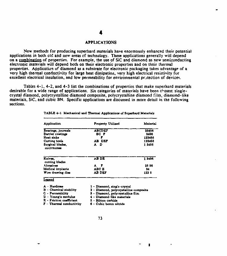
4
APPLICATIONS
New methods for producing superhard materials have enormously enhanced their potentialapplications in both old and new areas of technology. These applications generally will dependon a combination of properties. For example, the use of SiC and diamond as new semiconductingelectronic materials will depend both on their electronic properties and on their thermalproperties. Application of diamond as a substrate for electronic packaging takes advantage of avery high thermal conductivity for large heat dissipation, very high electrical resistivity forexcellent electrical insulation, and low permeability for environmental protection of devices.
Tables 4-1, 4-2, and 4-3 list the combinations of properties that make superhard materialsdesirable for a wide range of applications. Six categories of materials have been c_osen: single-crystal diamond, polycryst_iline diamond composite, polycrystalline diamond film, diamond-likematerials, SiC, and cubic BN. Specific applications are discussed in more detail in the followingsections.
TABLE 4-1 M*chanictl and Thermal ApplicationJ of Sup,rhswd Materials
Application Prop,rty Utilised Matarill
Bearings, journals ABCDEF 28456Bswri*r coatings BC F 3456H.at sinks F 12S456Cutting took AB DEF 123466Surgical blade, A D I $456microtonul
Knives, ._B DE 1 S456cutting bhtd_
AbrMiv_ A F 28 S6Medicalimplants ABC E 34Wire drawingdies AB DEF 123 5
hsum/
A - Hsrclnmm 1 - Diamond, sing!l-crystal
B - Chemical stability | - Disunond, polycrystallin, compo.,it.C - Permeability 3 - Diamond, polycrysttlline fl_mD - Young's modulus 4 - Diamond-like materials
E - Frictioncodfleiant 5 - SiliconcarbideF -Th.rmalconductivity 6 - Cubicboron nitrids
73
1990017647-085

74
TABLE 4-2 Electroni_ AppUcationJ of Superhard Materia TM
Application Property Utili_ Materild
TransistorsHigh-performsace Y LM 1 56High-temp4rsture BC F LMN 1 S6Radiation-hard F J LM I 56High-power F LMN I 56
Negative ,lKtron,Lffinitycathode J L 1 S
Ellctdcal inJulatom B JK M 1 3456Substrata, heat sinks F K M 1 SX-ray muks ABCD G 1 34
Dir_t-writemicrool_:tronics AB 4
Mztgnetic disks, h,_Is ABE 1 4Hifh-volta|e switchss F K M I SSThermistors F J 1 S 56P_:ksling A C F K M 1 34
Imsad
A - H_in_, 1 - Diamond, 8inEle-cr/stslB - Chemical stability I - Diamond, polyc_"veta_linecompositeC - Pemmability $ - Diamond, polycrygi_-UinefilmD - Younz'e modulus 4 - Diamond-like mat4wislE - Friction co_qicient S - Silicon carbideF - Thermal conductivity 6 - Cubic boron nitdd,G - X-ray trsnlmissionH - Infrarsd transmissionI - ViJibls trsnsmbeionJ - Ultraviolet transmission,
large bsnd-ppK - Electrically insulatingL - gemiconductivityM - Dielectric strengthN - Cm*riervelocity\mobility
Many of the potential applicationsof superhardmaterialsare currently limited byconditions during synthesis and by the propertiesof the resuitaqt product. In the c_e ofdiamond films, limiting factors are high substratatemperaturesduring dep,_si',ion;large surfaceroughnessesthat are undesirablefor many mechanicaland optical applications;poor adherencetosubstrata materials;and stresses in the films that can lead to delaminat:,onand substratafracture.
Other applicationsrequiresingle crystalsor epitaxial films. Single-crystal diamond filmshave been grown homoepitaxially on diamond;however, epitaxiai growth on other materials,which would be highly desirable, has not yet been confirmed. For electronics, one must be ableto dope with electrically active species to produce b<,,nn-type and p-type condvctivity. In thecase of diamond, there is a problemof how to incorporatesubstitutionaln-type dopants.
Finally, CVD deposition of polycrystaJlinebulk material,as opposed to thin film material,requireshigh deposition _'ates. Although high deposition rates have been reportedin theliterature, uniform deposition of high-quality materialover largeme:Lshas not yet been achieved.
1990017647-086
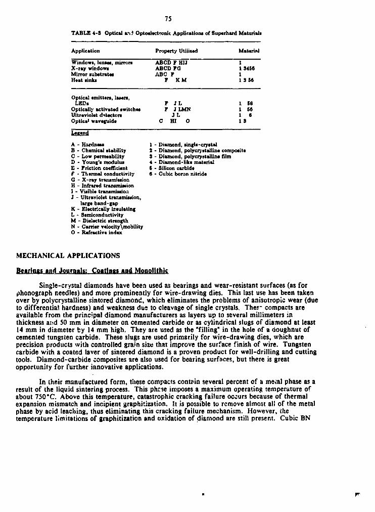
75
TABLE 4-$ Optical L.L40pto4dectronk Applications of guperhard Mat_riak
Application Property Utilis4d Materi_l
Windows, Icsmw, mirrors ABCD F HIJ 1X-ray windows ABCD FG 1 3456Mirror subatmtu ABC F IHeat sinks F K M I $ 56
Optical emitters, Immrs,LEDs F J L I 56
Optically activated switchm F J LMN 1 66Ultraviolet d_tectors J L 1 6Opticat wavquide C HI O I S
A - H-..rdnes* I - Diamond, single-crystalB - Chemic,.* stability 2 - Diamond, polycrystalline compoai_eC - Low pernmability $ - Diamond, polycrystalline filmD -Young', modulus 4 - Diamond-like materialE - Friction coefficient S - Silicon carbideF - Tl'.armal conductivity 6 - Cubic boron nitrideG - X-ray tr,ammJmdonH - lnfrsr, d traxmmi_ionI - Visible transmluio,._J - Ultraviolet trar.smi_ion,
larg, band-gapK - F.iectrlcally i_sulatingL - SemiconductivityM - Dielectric strengthN - Carrier velocity\mobilityO - Refractive index
MECHANICAL APPLICATIONS
Bearlnlsand Journals: Coatimzs and Monolithic
Single-crystal diamonds have been used as bearings and wear-resistant surfaces (as forphonograph needles) and more prominently for wire-drawing dies. This last use has been takenover by polycrystalline sintered diamond, which eliminates the problems of anisotropic wear (dueto differentia! hardness) and weakness due to cleavage of single crystals. Thes- compacts areavailable from the principal diamond manufacturers as layers up to several millimeters inthickness and 50 mm in diameter on cemented carbide or as cylindrical slugs of diamond at least14 mm in diameter by 14 mm high. They are used as the "filling" in the hole of a (toughnut ofcemented tungsten carbide. These slugs are used primarily for wire-drawing dies, which areprecision products with controlled grain size that improve the surface finish of wire. Tungstencarbide with a coated laver of sintered diamond is a proven product for well-drilling and cuttingtools. Diamond-carbide _,omposites are also used for bearing surfaces, but there is greatopportunity for further innovative applications.
In their manufactured form, these compacts contain several percent of a metal phase as aresult of the liquid sintering process. This phr.w imposes a maximum operating temperature ofabout 750"C. Above this temperature, catastrophic cracking failure occurs because of thermalexpansion mismatch and incipient graphRi_tion. It is possible to remove almost al; of the metalphase by acid leaching, thus eliminating this cracking failure mechanism. However, thetemperature l;mitations of graphitization and oxidation of diamond are still present. Cubic BN
• rr
1990017647-087

76
can be used at higher temperatures than diamond. Surface fluorination is being used to enhancethe oxidation resistance of diamond (Margrave, et al., 1988).
m
Some of the ;,dvantages seen for CVD diamond layers in bearing and wear-surfaceapplications are higher thermal stability, which will aid both in use and in brazing to substrates;essentially theoretical density (no metal phase, no porosity from metal removal); ability to makeintricate shapes; arid potential of making smooth, mirror-like surfaces without polishing.
The high thermal conductivity of some of the superhard materials (diamond, cubic BN,SiC) can decrease wear significantly by rapid transfer of heat from hot spots caused by localizedfrictional heating. Diamond and diamond-like materials both have shown small coefficients offriction (<0.0_), which also acts to minimize frictional wear (Koskinen et al., 1985; Miyake et al.,1985).
In the case of diamond-like materials, the coefficients of friction depend on the relativehumidity (RH). Up to about 1 percent RH, the coefficients are very low (0.01-0.02); however,above I percent RH the coefficients increase rapidly, reaching 0.2 at 100 percent RH (Tsai andBogy, 1987). The coefficient of friction of diamond is less sensitive to moisture. In the case ofdiamond, adsorbed hydrogen appears necessary to maintain the low coefficient of friction.However, in a vacuum envircnment or at high temperatures, this hydrogen layer will desorb,resulting in a significantly higher coefficient of friction.
Although diamond-like films are very smooth, CVD diamond usually has a rough surfacethat would act toabrade an opposing part. Deposition of smooth CVD diamond films wouldsolve this problem. The nonreactivity of superhard materials in corrosive environments end athigh temperateres makes possible the fabrication cf bearings and journals that can overate inadverse env;ronments such as those found in nuclear reactors.
The ability to deposit diamond, DLC, and cubic BN in thin film form should allow forcoating large surface areas for abrasion and wear resistance. Thus, for example, it may bepossible to produce diamond-coated ways, spindle bearings, and shafts on milling machines andlathes. The decrease in wear of such components would result in equipment that maintains smallm_chining tolerances over significantly greater periods of time than at present.
Nonreactivity in corrosive environments, at high temperature, and in the presence ofionizing radiation may make it possible to use some superhard materials as protective barriercoatings in adverse environments. Tl',eir low permeability would prevent diffusion of reactivespecies to the substrate material, thus Dreventing substrate degradation. High thermalconductivities would diffuse hot spots, preventing localized high temperatures from reaching thesubstrate.
._ttine Tool_ Drills. Bits. Cultters.Saw Blade_
Precision turning tools made of polycrystalline diamond are still of limited value becausethe grain size is larger than the des;red surface finish in most cases. This is less of a problem indirect-cc,_verted polycrystalline materials (i.e., gr_'phite converted directly to diamond withoutsolvent catalysts, or hexagonal BN converted to cubic BN). CVD diamond and cubic BN are veryattractive for this application because of the possibility of having very-fine-grain materiel orsingle crystals deposited and b.3n,Jed directty onto the tool material.
1990017647-088

77
Surgical Blades and MIc;gtomel
Single-crystal diamond is already used for microtome blades and surgical knives. Thesharpness of the blade allows cutting of biological tissue without significantly depressing thetissue (minimum springback), and the hydrophobic surface of diamond prevents sticking anddragging. The production of large synthesized single crystals was at first aimed primarily at thismarket and the turning tool market. The limitations here are primarily associated with thedifficulty of grinding and polishing uniform edges. It is expected that eventually the CVDprocess could be used to produce a uniform edge directly, without a polishing procedure, andthereby solve this problem.
Knives and CuttiH Blades
There are applications for diamond cutting blades in a wide variety of industries. Forexample, the orange juice industry requires cutting blades that maintain their sharpness for anextended length of time. Dull blades waste the juice in the oranges. At the present time, thesecutting blades, which are made of a hard stainless-steel alloy, require sharpening every 30 days.If the blades could last for a full cutting season of 9 months without sharpening, considerable [_.sa _ngs wou',d result. Coating the cutting blades with diamond or DLC would appear to be oneway of extending the time between sharpenings.
Abrasives
Diamond grain and cubic BN abrasive grain were the first synthesized superhard materialsproducts. Sintered polycrystaUine materials followed. Manufacturers in about 14 countries makegood-quality abrasive grain that ends up mounted in various media for cutting, grinding, andsawing applications. Grain sizes range from submicromecer scale to almost I ram. The largersizes are used primarily for rock cutting and shaping. Synthesized abrasive grain can be providedreproducibly with controlled properties--size, shape, toughness. I) is for this reason that about90 percent of industrial diamond is synthesized and i0 percent is vatural.
The potential of CVD diamond for abrasive grain is now being evaluated by variousmanufacturers. It will probably find a unique niche in the market by virtue of its purity, shape(i.e., flakes and sheets are possible), and polycrystaUine nature. Its defect structures may giveCVD diamond different and perhaps better abrasive properties.
Medical Imniants
Ion beam-depositedDLC coatings have been studied for their use in b_.ological impiantsystems (Aisenber8 and ChaboL 1974). The coatings produced were found to have an extremelysmooth surface, high surface tension, and slight elf,ctronegativity (Adamson, 1982). In addition,the samples were found to have a low gas permeability and high adhesion to the substrates tested.Result,_ of veaa tara, renal embolus, and ex )'ivo tests indicate a high degree of thromboresistancefor these materials, These results combined with the durability of the m_terials suggest that theycould be useful as coatings for medical implants, including artificial joints. One would expectthat diamond coatings would perform in a similar manner. The high surface energy of diamond,which causes it to be hydrophobic, allows it to _esist bacterial and viral attachment, since surfaceenergy relates to _urface tension (Adamson, 19821
1990017647-089
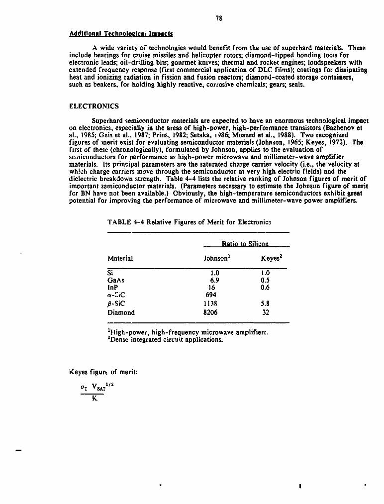
78
Ad01tlonal TechnoloEical Imuacts
A wide variety of technologies would benefit from the use of superhard materials. Theseinclude bearings for cruise missiles and helicopter rotors; diamond-tipped bonding tools forelectronic leads; oil-drilling bits; gourmet kmves; thermal and rocket engines; loudspeakers withextended frequency response (first commercial application of DLC films); coatings for dissipatingheat and ionizing radiation in fission and fusion reactors; diamond-coated storage containers,such as beakers, for holding highly reactive, corrosive chemicals; gears; seals.
ELECTRONICS
Superhard semiconductor materials are expected to have an enormous technological impacton electronics, especially in the areas of high-power, high-performance transistors (Bazhenov etal., 1985; Geis et al., 1987; Prins, 1982; Setaka, 1_86; Moazed et al., 1988). Two recognizedfigures of merit exist for evaluating semiconductor materials (Johnson, 1965; Keyes, 1972). Thefirst of these (chronologically), formulated by Johnson, applies to the evaluation ofsemiconductors for performance as high-power microwave and millimeter-wave amplifiermaterials. Its principal parameters are the saturated charge carrier velocity (i.e., the velocity atwhich charge carriers move through the semiconductor at very high electric fields) and thedielectric breakdown strength. Table 4-4 lists the relative ranking of Johnson figures of merit ofimportant semiconductor materials. (Parameters necessary to estimate the Johnson figure of meritfor BN have not been available.) Obviously, the high-temperature semiconductors exhibit greatpotential for improving the performance of microwave and millimeter-wave power amplifiers.
TABLE 4-4 Relative Figures of Merit for Electronics
Ratio to Silie,on
Material Johnson z Keyes z
Si 1.0 1.0GaAs 6.9 0.5InP 16 0.6a-_iC 694
fl-SiC I 138 5.8Diamond 8206 32
ZHigh-power, high-frequency microwave amplifiers.ZDense integrated circuit applications.
Keyes figurL of merit:
oz V_T 1/z
K
1990017647-090
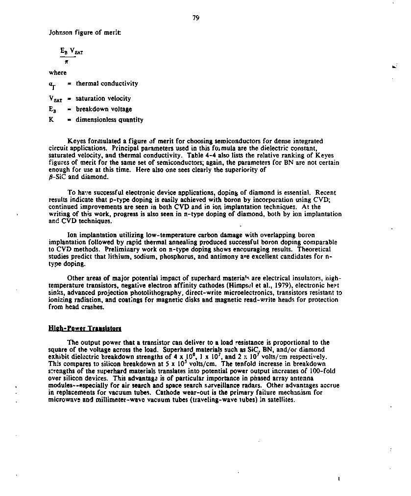
79
Johnson figure of merit:
E_ VSAT
ff
where
aT = thermal conductivity
VSA_ = saturation velocity
Ee = breakdown voltage
K = dimensionless quantity
Keyes formulated a figure of merit for choosing semiconductors for dense integratedcircuit applications. Principal parameters used in this for mula are the dielectric constant,saturated velocity, and thermal conductivity. Table 4-4 also lists the relative ranking of Keyesfigures of merit for the same set of semiconductors; again, the parameters for BN are not certainenough for use at this time. Here also one sees clearly the superiority ofE-SiC and diamond.
To ha,,e successful electronic device applications, doping of diamond is essential. Recentresults indicate that p-type doping is easily achieved with boron by incorporation using CVD;continued improvements are seen in both CVD and in ion implantation techniques. At the
, writing of this work, progress is also seen in n-type doping of diamond, both by ion implantationand CVD techniqu=s.
Ion implantation utilizing low-temperature carbon damage with overlapping boronimplantation followed by rapid thermal annealing produced successful boron doping comparableto CVD methods. Preliminary work on n-type doping shows encouraging results. Theoreticalstudies predict that lithium, sodium, phosphorus, and antimony are excellent candidates for n-type doping.
Other areas of major potential impact of superhard materia!_ are electrical insulators, ifigh-temperature transistors, negative electron affinity cathodes (Himpsol et al., 1979), electronic hePtsinks, advanced projection photolithography, direct-write microelectronics, transistors resistant toionizing radiation, and coatings for magnetic disks and magnetic read-write heads for protectionfrom head crashes.
Hlth-Power Transistors
The output power that a transistor can deliver to a load resistance is proportional to thesquare of the voltage across the load. Superhard materials such as SiC. BN, and/pc diamondexhibit dielectric breakdown strengths of 4 x 10s, 1 x 10⁷, and 2 r. 107.volts/:m respectively.This compares to silicon breakdown at 5 x l0 s voits/cm. The tenfold increase in breakdownstrengths of the superhard materials translates into potential power output increases of 100-foldover silicon devices. This advantage is of particular importance in phased array antenna
, modules--especially for air search and space search surveillance radars. Other advantages accruein replacements tbr vacuum tubes. Cathode wear-out is the primary failure mechanism formicrowave- and millimeter-wave vacuum tubes (traveling-wave tubes) in satellites.
I
1990017647-091
80
Hi=h-PerfQrmance (Ranid-Resoonse_ Transistors
Several factors affect transistor speed. Among them are dielectric constant, charge carriermobility, and charge carrier velocity. The dielectric constant determines the parasitic capacitanceof the transmission lines on integrated circuits. Phase distortion and propagation speed areadversely affected by a large parasitic capacitance. The dielectric constants for diamond and SiCare 5.5 and 9.0, respectively, compared to 12 and 1"3for silicon and germanium, respectively.Speed/frequency performance is inversely related to the dielectric constant; therefore, thesuperhard materials provide advantages in applications involving supercomputers and solid-statepower amplifiers in the microwave and millimeter-wave spectrum.
Modern transistors require lithographic resolutions of less than 1.0 micrometer and arecharacterized by charge carrier channel regions of similar dimensions. These very short channellengths lead to electric field strengths of 50,000 volts/cm in logic devices and even greater fieldsin analog devices. Since the superhard materials have ,ower atomic mass than more conventionalsemiconductors, the energies of the optical phonons that scatter the charge carriers are muchhigher. The ve!ocities at which the charge carriers (i.e., electrons and holes) are scattered byoptical phonons is thus much higher, and charge carrier transit time across the transistor channelis therefore shorter than in semiconductors characterized by higher atomic mass. Transit timegain factors of 2 to 3 over silicon and GaAs are possible. This translates directly into apropc'tionately higher frequency response.
Although charge carrier mobilities exhibited by diamond and SiC are generally lower thanthose of conventional semiconductors (an exception is the hole mobility of diamond, which is 3times the hole mobility of silicon), this limitation can be circumvented by using cascade-structured devices, wherein the charge carrier velocity entering the second stage of the device isnear saturated velocity. In this manner the average velocity of electrons in diamond and SiC canbe much higher than that of even GaAs.
A final speed and frequency advantage of diamond and SiC over I[I-V semiconductordevices arises because the superhard semiconductors do not exhibit a region of negativedifferen'ial conductivity. As such, the charge carrier velocit,, remains high, even at high electricfield strengths. This equates to higher-power microwave and millimeter-wave amplifiers.
Hi__g_-TemneratureTransistors
" The large forbidden band-3aps of diamond, SiC, and cubic BN enable them to continue toact as semiconductors at extremely high temperatures without experiencing charge carrierdegeneration. Temperatures as high as 650"C have been demonstrated for E-SiC; BN anddiamond should perform at even higher temperatures. Practical upper opecating temperatureswill be limited primar:ly by degradation in the metallization used for ohmic and Schottkycontacts to the semiconductors.
High-temperature transistors will be particularly advantageous in spacecraft In unmannedspacecraft, _he systems required to cool conventional silicon eevices to 125°Ccould be largelyeliminated if operating temperatures of 325"Cwere permissible. These cooling systems canoccupy up to 60 percent of the volume of an unmanned satellite. Thus the use of semiconductorssuch as SiC, cubic BN, and/or diamond could significandy reduce the system vo'ume, weight,and cost. However, the advantages, compared to silicon *'_d GaAs, may be offset because them,_bilities of the negative free carriers (holes) a,_gear to decrease more rapidly with increasingtemperature than those of silicon and GaAs.
1990017647-092

81
Rg41ation-Hard Transistors
The binding energies between the atoms of superhard crystals are much stronger than thoseof the more conventional semiconductors. Therefore, their vu!nerability to heavy particle (ion)bombardment is less than that of conventional semiconductors. Furthermore, because of theirhigher band-gaps, fewer electron-hole pairs are generated per impinging photon; again thistranslates into _sreater immunity to alpha, beta, and gamma radiation. Definitive tests ondiamond and BN devices have not yet been conducted because of the embryonic state of the art.Preliminary tests on synthetic epitaxial and natural diamond indicate a factor of 100 improvementin the damage resistance over that of silicon to 1.5 meV electrons, Initial Japanese tests on/3-SiC devices have shown them to be immune to a radiation dose of 107 tad equivalent in silicon,radiation sufficient to damage most silicon devices, If fused silk,,- is esed as the insulator for SiCdevices, the fu_ed silica an_ not the SiC will be the limiting factor in radiation immunity.Fortuitously, AIN is lattice-matched to SiC and may be useful as a heteroepitaxial insulator,enabling SiC to operate in a potential well of the single-crystalline AIN insulator. If so, it maybe possible to fabricate insulated-gate field-effect transistors that do not have the limitations ofpresent SiO2-based silicr_n devices. Similarly, diamond devices may be made to operate in a9otential well created by lattice-matched cubic BN insulators. A significant amount of researchwill be required before these aspects of inherent radiation hardness can be confirmed.
The combinatio_l of radiation hardness and high-temperature capability of superhardmaterials may make electronics practical within or near nuclear reactors.
Hi_h-VoltHe Electronics
High-voltage electronics made from superhard semiconductor materials would have greaterreliability than vacuum tubes, the components most likely to fail in high-voltage circuits. Thiswould be extremely important for phased array antenna modules and satellites. Megavoltswitches would h? reliable because superhard materials have high breakdown voltages. Thiswould facilitate _mplementing high-voltage dc transmission of electricity.
Reliable Electronics
The predominant failure mechanJsm in power semiconductors is the migration (diffusion)of dopant impurities. The superhard semiconductors have a decided advantage in this respect.The diffusivity of dopant impurities in the superhard materials at temperatures well above therr_Iting point of silicon is equivalent to the diffusivity of dopants in silicon at 125"C. Attemperatures well above 400-C, im_,urity diffusion in the superhard semiconductors is negligible.The predominant failure mechanism will be solely that of the metallization. The use of metalsilicides and metal carbides i,,.expected to significantly improve resistance to even thisdegradation mechanism. However, low diffusivity may be a problem when trying to obtain
,_ uniform semiconductor doping.
NHative E[e_;_ronAffinllv Cathodel
Diamond is believed to have a negative electron affinity (Himps,-I et al., i979). Thisshould make possible efficient _lectron emitters for a variety of applications, such as elec-yronguns with cold cathodes and micrometer-sized vacuum tubes tha: would have power an_frequency performance far superior to that of conventional semiconductor devices.
1990017647-093

82
Electrical Insulators
Superhard semiconductor ,_qaterialsgenerally possess large forbidden band-gaps andtherefore are good electrical insu!2tors. Natural diamond, for instance, can exhibit darkresistivitiesgreater than 10z° ohm-cm resistance. In synthesized diamond, resistivities varybetween 10Q-and 10l° ohm-,:m, depending on the growth process used. The insulating propertiesof semiconducting heterojunctions must, however, be considered on a case-by-case basis.Depending on how the band-gaps align, the material with the wider band-gap may notnecessarily be an insulator for both electrons _,nd holes. The view of semiconductor-insulatorinterfaces must be modified to a concept of assessing materials in potential wells. Diamond-likematerials can have resistivities exceeding 1012 ohm-cm.
Heat Conductors
Most of the superhard materials useful for electronic applications also have high thermalconductivities. For example, natural diamond has a value of 20 Wcm-1 K-x at room temperatur_(Ono et al., 1986). Since natural diamond contains both carbon 12 and carbon 13 isotopes, itsthermal conductivity is not optimized. Isotopically pure carbon 12 diamond should have athermal conductivity that is greater by a factor of 2, but experimental verification of thisprediction is needed.
BN, SiC, and AIN are also good thermal conductors and are of use in a variety ofapplications. These materials a_e most useful in single-crystal form, heteroepitaxially bonded tothe material to which they are to be used as heat sinks. However, heteroepitaxy is believed to belimited to lattice-matched materials with similar chemical bonding. BN is only lattice-matched todiamond, and SiC is only lattice-matched to/_IN and GaN. Most applications will require otherforms of bonding, such as soldering.
Unlik,. copper, the superhard heat sinks are generally electrically insulating in nature andcan be used for removing heat without the complicating requirement of an additional electricallyinsulating layer. The high heat-removal capability of these materials should permit the
" fabrication of integrated circuits with significantly increased coml._onent densities.
X-RAy Masks for Advance Pr61ectlon Photolitho_ranhv
X-ray wavelength masks offer the possibility of achieving si;'nificantly higher-densityelectronics. These masks must be thin to prevent absorption of the x-ray radiation and yet mustbe optica"y _,ransparent for visoal observation. Large areas of thin unsupported diamond filmswill be required.
Direct-Write Microelectronics
Coating of electronic chips during processing with diamond-like coatings can be used topattern the electronic circuit cfirectly--for example, by electron beam etching.
_isks and Read-W,.'-le Heads
Magnetic disks and read-write heads are susceptible to damage when the head comes intocontact with the magnetic medium. The result can be destruction of the disk, the head, and
1990017647-094

83
valuable stored data This problem is becoming even greater as attempts are made to increase thedensity of Gataon the storage medium, requiring smaller head-to-disk _aps. The disk and headmust be protected with a wear-resistant, low-friction coating. Much of the earlier discussionconcerned with friction and wear in bearings and journals is applicable here. Coating of disksand heads with DLC has been the subject cf extensive study, and a considerable payoff in saveddata may be realized (Tsai and Bogy, 1987).
Additional Technological Imoacts
Additional advantages of superhard electronic materials include in situ electronic sensingand signal processing in chemical reactors, automobile engines, engines in heavy industrialequipment,rocketengines,nuclearreactor-s,etc;low=costmicrowaveovens;higher-speedsupercomputers;nuclearradiationdosimetersand detectorswithgreatpotentialforuseinradiationbiologyand medicine;and t_ermistors.
OPTICS AND OPTOELECTRONICS
The desirability of superhard mate_ials as optical materials stems from their uniqueproperties. Their advantages apply both to monolithic optics and to optical coatings. Theirprimary advantages lle in their hardness and chemical inertness, which would make opticalcomponents fabricated from these materials resistartt to adverse conditions such as abrasiveenvironments caused by dust and rain, chemically corrosive environments, reactive environmentsas in plasmas, and high-temperature environments. In addition, particular materials would haveother advantages. The wide band gaps of diamond and cubic BN make them candidates forultraviolet optics, and their low mass numbers make them candidates for soft x-ray windows.High thermal conductivity, high Vomit,'., modulus, low therm_,l expansion coefficient, and h;gnfracture toughness make diamond an i,,,;portant candidate material for optical components inhigh-photon-flux environments, such as in free-electron I_ers, because of its resistance tothermal fracture and its ability to dissipate heat rapidly. Table 4-5 shows the figures of merit forthermal stress resistance of diamond relative to those of several important opti:al materials,Diamond is clearly superior to the other materials, from both a _ractical and a theoretical pointof view.
Several major problems must be overcome before diamond optics in the nza_-infrare0,visible, and ultraviolet w:,ll be widely used. In the case of shlgle-crystal diamond, ,3.._lylimitedsizes are available, perhaps up to 7 cm in diameter. CVD diamond could be vsed i/" aonolithicoptics (such as lenses, windows, and domes), provided deposition rates were sufficiently high. I_the case of CVD diamond, however, the limitations are optical scatter arising from polycrv_.rallinemorphology and surface roughness and absorption resulting f_'om graphitic or diamond-likespecies, lattice defects, and other impurities within the diamond phase.
Crystalline diamond and diamond-like materials have many potential uses as coatings forinfrared optics. In principle, diamond shows no first-orc_er absorption in the infrared; theabsorption observed is due to second-order processes, deftcts, and impurities. Diansond coatingsare potentially applicable for use from the ncnvacuum ultraviolet through the infrared, except fora region of ,_bsorption between 2.5 _nd 6 _,n, but optical scatter limits such use in currentlyproduced CVD diamond. However, at wavelengths beyond approximately 10 _,m, transmissionmeasurements sun,eat that this material may have adequate transmissivity to be useful in theIongwave infrared region.
1990017647-095

84
FABLE 4-5 Figures o_"Merit for Thermal Stress Resistance
Material RT Source
Silicate glass 2.3 x 10z aSapphire 3.4 x 10³ a -Fused silica 4.3 x l03 aDiamond (300 K) 9.4 x 10⁵ b
( 80 K) 1.3 x 10⁷ b(300 Y_) 3.8 x I08 c(80K) 5.4x 10⁸ c
a.From Krupke etaL (1986),inwhicha flawsizeof50 _,wwas assumed.
b.Basedon parametersinField(1979)and assuminga flawsizeof 50 _,m.
c.Theoret;calvaluebasedon paraL_etersinField(1979).
_r - ._ x(l-u)aE
wheret
R: - figure of meri:
o_ - fracture strength
- thermal conductivity
u - Poisson's ratio
c: - linear therraz: expansioncqefficient
E - Young's modulus
The use of CVD diamond as an optical film material has the :im,_tation of re0uiring high' substrat_ temperatures (greater than 600"C)ducing deposition, whic_ restricts the number of
substrate materials that can be used. Adhesion to the substrate is anuther problem, _.nd, when thediamond does adhere, c_ifferential contraction during cooling can lea:l to delamination andcrazing. Diamond-,ke films, on the other hand, can be deposited at much lower temperatures(approximately 150"C).but they too exhibit adhesion problems and may also contain largeinie,,'nal stresses that can cause delamination of thick coatings from subst-ates. Hydrogen-freeDLC coatiugs have much less residual stres', than the DLHC type, however.
_Jme of _he early adherence problents have been addressed wit.'-,t_ood results. Fore,arn¢ie, tl:e adherence of diamond-like rilms to infrared-transmitting substrates such as ZnS andZnSe is improved dramatically by de_ositir, g an amorr_hous geratanium-carbon layec between thesub_trate and the overlying diamond-like ,.rating (Lettington et. al., 1987; Wort and Lewis, 1987).
1990017647-096

85
This combination of hard coatings can imnart good wear erosion and abrasion resistance to ZnSand ZnSe and can be adjusted in thickn.e, • to provide an antireflection coating as well.
In addition to their potential use as optical coatings and monolithic optics, superhardmaterials h_ve potential uses as mirror subs*.rates,optical and optoelectronic heat sinks, lasersources, light-emitting diodes (visible and ultraviolet), high-speed optically activated electronicswitches, ultraviolet detectors, optical waveguides, and fiber optic coatings.
_.hi¢ Windows and Leases
The ability to deposit high-optical-quality CVD diamond at high deposition rates will makeit possible to produce windows and lenses for the infrared, visible, and ultraviolet that aredurable in extreme environments. In addition to the environn_*,ntal advantages of diamond, itshigh refractive index makes it an attractive lens material because lenses with high refractivepower can be made significantl,t thinner and hence lighter. Furthermore, simp'.e antireflectivecoatings can be easily made for diamond optics, especially for the ultraviolet, because theantireflection condition is more easily satisfied than for other substrate materials. For example, asingle-layer antireflection coating, to work efficiently, must have a refractive index close to thesquare root of the substrate refractive index, _ condition difficult to achieve for substraterefractive indices less than 1.9. The refractive index of diamond at 0.589/_m is 2.418; a filmwith an index of 1.555 would make an alr.tost perfect antireflection coating, a value easilyobtainable with optical glasses. In addition, diamond and DLC make good infrared antireflectioncoatings for substrate materials such as GaAs, silicon, and germanium.
, Single-crystal diamond has particular advantages as a high-power laser window or outputcoupler, such as is required in a free-electron laser. Because of its superior thermal shockresistance and its large heat-dissipation capability, it may make possible very compact free-electron lasers. With diamond windows the areal power density could be higher, resulting ingreater total power for a given beam size. If the windows are cooled to liquid-nitrogentemperatures, the heat-dissipating capability of diamond windows would be even greater. Thus,an effort to produce large, high-optical-quality single-crystal diamond either by high-pressuretechniques or by CVD processes would be extreme ._..lesirable.
Because of the low atomic numbers of the elements in diamond, DLC, DLHC, and BN,these materials exhibit low x-ray absorption, making them excellent x-ray windows. Because ofits high strength, diamond can be made very thin, thus lowering its absorptivity even more. Inthe soft x-ray region, diamond would be expected m replace beryllium. Commercialization ofdiamond for energy-dispersive anaylsis windows for energy-dispersive x-ray analysis is expectedsh,_rtly.
Mirror Substrates
High thermal conductivity and high strength make diamond an excellent substrate materialfor mirrors intended for high-average-power laser radiation. The high strength would allow forthinner substrates and hence lighter mirrors. This will be practical when large-diameter, thickdeposits can be made at reasonable deposition rates.
1990017647-097
86
Heat Conductors
Diamond, SiC, cubic BN, and AIN can act as heat-conducting substr_te materials foroptoelectronic applications such as laser diodes, where significant heat may be developed. In thiscase the constraints are similar to the electronic ones discussed earlier. The use of superhardmaterials as mirror substrates, as discussed above, takes advantage of their large thermalconducting capabilities.
ODtical Emitters. Lasers. and Li2ht-Emittin2 Diodes
SiC and cubic BN, because of their large dilect band-gaps, emit optical radiation atsignificantly shorter wavelengths than conventional III-V materials. BN has recentlydemonstrated emission in the ultraviolet. Furthermore, it is expected that light-emitting diodescan be made from these materials. In diamond, direct laser action is expected to be moredifficult because it is an indirect band-gap material. However, laser action has been exhibited bycolor centers in diamond (Rand and DeShazer, 1985a, b) in the visible region; thus, diamond canact as a laser host material. Calculations indicate that, by applying a large uniaxial strain todiamond, it can be converted to a direct band-gap semiconductor. Whether such a large uniaxialstrain can be I_roducedand maintained in practical device:_ is highly problematical. Perhaps itcan be accomplished by making diamond one component of a strained-layer superlattice. Otherpossibilities for laser action in diamond are intra-atomic energy transitions (2d and 4f) inimpurity ions within the diamond or within a heterojunction p-n junction. Ultraviolet lasersmade of superhard materials offer greater storage density capability on compact disks because thelaser light could be focused to smaller spot sizes.
Onticallv Activated Electronic Switches
Recent experiments have shown that diamond can act as an optically activated electronicswitch (Bharadwaj et al., 1983; Young et al., 1983; Glinski et al., 1984; Huo et al., 1986). Becauseof its high breakdown voltgge, diamond can withstand very high voltages without electricalbreakdown, lllumiriation by intense excimer laser radiation leads to switching time_ on ananosecond time scale and smaller.
Ultraviolet Solar-Blind I)eteflori
In the region between 180 nm and 300 nm, the ozone layer reduces the reflectance of theearth over 3 orders of magnitude below that of the visible and near-infrared. In the region of140 to 180 nm, the reflectance is further reduced by an additional 200-fold. Below 140 nm, auralspectra dominate. For exoatmospheric "targets"a truly solar-blind region is the window at 140 to180 nm. Although the band-gap of cubic BN is not now known with certainty, it is expected tolie within this window. Since BN has now been synthesized in its cubic form, the excitingpossibility exists that BN can be used not only _ a solar-blind detector but also as a coherent(laser) illuminator as well. Diamond should be blind to radiation at wavelengths longer than 225nm and thus can be used to capitalize on the more than 3 orders of magnitude ozone-createdreduction in the solar reflection of the earth. SiC has too low a band-gap to be useful in solar-blind applications.
1990017647-098
87
Onti¢al Waveiuides
The high refractive index of diamond makes it a candidate optical w_veguide material.Because it is a centrosymmetric material, it will not exhibit an electro-optic effect; thus, it mightbe useful either as a passive waveguide material or as ar_acousto-optic material. Furthermore,the refractive index of diamond is between the refre:;ive index of C,aAs and related III-Vcompounds used as optical sources and that of LiNbO3, a modulator material. Thus, diamond canact as a transition waveguide between components made of these two classes of materials.
I_iberOntlc Coatine
Fiber optics are subject to abrasion and chemical degradation from moisture. The strengthof silica=based fibers is severely lowered by water vapor. Hard, impervious coating materials areneeded to protect these fibers. Both diamond and diamond-like carbon are hard, providingabrasion resistance. In addition, because they are dense and chemically impervious, they can beused to hermetically seal a fiber from the environment. Fiber optics coated with DLC areeffectively sealed against w;Rer-vapor penetration. This will be especially important for the newheavy=metal halide fibers that exhibit low absorption in the infrared but are particularlysusceptible to environmental degradation, especially moisture. Optical communications systems,including military systems, rely heavily on fiber optics.
l had_.Caatlau
High-Power Laser Mirrors
Laser mirrors are subject to degradation from a variety of sources: They are subject tointense optical radiation, which causes a form of dielectric breakdown owing to the high opticalelectric fields present; they are subject to thermal shock and degradation as a result of heating bythe intense optical radiation; they are subject to attack by reactive s_cies such as fluorine inexcimer lasers; they are subject to plasma erosion in lasers with gas discharges; and they aresubject to environmental degradation from dust and moisture whe_, they act as the output couplerto the external environment. Furthermore, many lasers operate in the ultraviolet, where there is alack of hard coating materials possessing high refractive indices. Because of the high refractiveindex of diamond and its resistance to environmental attack, the development of low-optical-loss diamond coatings in single layers and in multilayers with other lower index materials such asSiOz would considerably ameliorate these problems. The high refractive index of diamond shouldmake possible antireflectin8 and high-reflecting mirrors with fewer layers and with greatersurvivability than current mirrors.
Protective Coatings
Many optical components are subjected to extreme environmental factors that causecomponent degradation. Much of this degradation occurs in environments of critical importanceto the nation's defense. Aircraft fly through dust and rain, which abrade and erode aircraftcanopies; tanks and personnel operate in dusty and moist environments that degrade viewingports, binoculars, periscopes, rangefinders, target designators, and goggles; radomes and IR-domes are subjected to dust and rain impact and abrasion and may be heated to elevatedtemperature because of atmospheric friction.
1990017647-099

83
He:'_ng of radomes in re-entry vehicles can be a problem because the high temperaturesgenerated _a the atmosphere can cause the ra_Iomematerial to become conducting, which preventsthe transmission of microwave energy owing to absorption. In this situation diamond r_domeswould have four advantages: because of its large band-gap, diamond would remain insulating toelevated ten:oeratures, the low dielectric constant of diamond :esults in low reflectivity ofmicrowave energy because of a lower impedance mismatch with the air, the high therm_Iconductivity of diamond would permit generated heat to dissipate over a larger ares, thuslowering peak temperatures, and oxidation of the diamond surface would cause production of COand CO2, with the result that the chemical composition of the radome surface would remainunchanged.
From a commercial viewpoint, superhard protective optical coatings would be useful onalmost all optical surfaces. Diamond-coated eyeglasses, windshields, and windows couldsignificantly maintain visibility by decreasing the susceptibility to scratching. The lifetimes ofoptical disks would be significantly extended. Improvement by a factor of 6 h, scratch resistancehas been obtained for plastic lenses coated with DLC.
Antireflection Coatings
A.ntireflectioncoatingsofdiamondorDLC wouldhaveconsiderableadvantages.Siliconand GaAs solarcellscoatedwithdiamondwould exhibitgreaterefficiencybecauseofreductionofreflectivelosses,whileatthesame timethecellswouldbe resistanttodegradationfrom theenviro,mentoDLC coatingshavebeendepositedon siliconsolarcellswithan increueincellefficiencyof 40 l_r.centand on germaniumwindows,resultinginexcellenttransmissivity,TheadvantageofDLC coatingsoverdiamondisthattherefractiveindexof DLC can be tailoredtosuita particularapplication.Valuesof refractiveindexbetweon1.8and greaterthan2.I areobtainableby varyingthedepositionconditions,Moreover,DLC coatingsshow a negligiblesurfaceroughness,
Additional Technolo21cal Imnacts
Additional advantages that may arise from the application of superhard materials to opticsinclude environmentally stable interference filters; missile detection sensors; and detectorsresistant to ionizing radiation.
REFERENCES
Adamson,A.W. 1982.PhysicalChemistry,FourthEdition.New York:JohnWileyand Sons.
Aisenberg, S., and R. W. Chabot. 1974. Ion Beam Deposited Carbon Coatings for BiocompatibleMaterials. National Institute of Health, Contract No. NIH-NOL-HB-3-2919.
BaLhenov, V. K., I. M. Vikulin, and A. O. Oontar. 1985. Synthetic diamonds in electronics(review). SOy. Phys. Semicond., Vol. 19, pp. 829-841.
Bharadwaj, P. K., R. F. Code, H. M. van Driel, and E. Walentynowicz. 1983. High voltageoptoelectronic switching in diamond. Appl. Phys. Lett., Vol. 43, pp. 207-209.
1990017647-100

89
Field, J. E. 1979. The Proper,ties of Diamond. Loncion: Academic Press. M. W. Geis, D. D.Rathman, D. J. Ehrlich, R. A. Murphy, and W. T. Lindley.1987. High-temperature point contact transistors and Schottky diodes formed ot_ syntheticboron-doped diamond. IEEE Electron Device Letters, EDL-8, pp. 341-343.
Glinski, J., X. J. Gu, R. F. Code, and H. M. van Driel. 1984. Space-charge induced• optoelectronic switching in lla diamond. Appl. Phys. Lett., Vol. 45, p. 260.
Himpsel, F. J., J. A. Knapp, J. A. van Vechten, and D. E. Eastman. 1979. Quantum photoyieldof diamond(l II)-A stable negative-affinity emitter. Phys. Rev. B, Vol. 20, p. 624.
Huo, Y. S., X. J. Gu, R. F. Ccae, and Y. G. Fuh. 1986. Optical switching mechanisms in typella diamond. J. Appl. Phys., Vol. 59, p. 2060.
Johnson, E. D. 1965. RCA Rev. Vol 26, p. 163.
Keyes, R.W. 1972. Figure of merit for se_,iconductors for high-speed switches. Proc. IEEE,VoL 60, p. 225.
Koskinen, J., J. P. Hirvonen, and A. Anttila. 1985. Wear and hardness of diamond-like coat;ngsprepared by ion beam deposition. Appl. Phys. Lett., Voi. 47, p. 941.
Krupke, W. F., M. D. Shinn, J. E. Marion, J. A. Caird, and S. E. Stokowski. 1986. J. Opt. Soc.Am. B, Vol. 3, p. 102.
Lettington, A. H., J. C. Lewis, C. J. H. Wort, B. C. Monachan, and J. R. Hope. 1987.Developments in GeC as a durable coating material. In Proceedings of the E-MRS Meetingon Amorphous Hydrogenated Carbon Films, Strasbourg, June 1987.
Margrave, J. L., D. E. Patterson, and R. N. Hauge. 1988. Proceedings MRS Symposium, Boston,MA (December).
Miyake, S., S. Takahashi, I. Watanabe, and H. Yoshihara. 1985. Friction and wear properties ofhard carbon compo.-ed of diamond and graphite mixed crystal structure deposited ontovarious substrates. Pp. 407-412. Proc. JSLE International Tribology Confonference, July8-10.
Moazed, K. L., R. Nguyen, and J. R. Zeidler. 1%8. Ohmic contacts to semi-conductingdiamond. IEEE Electron Device Letters, Vol. 9, pp. 350-351.
Ono, A., T. Baya, H. Funamoto, and A. Nishikawa. 1986. Thermal conductivity of diamondfilms synthesized by microwave plasma CVD. Jap. J. Appl. Phys, Vol. 25, p. L808.
Prins, J.F. 1982. Bipolar transistor action in ion implanted diamond. Appl. Phys. Lett., Vol. 41,pp. 950-952.
Rand, S. C., and L. G. DeShazer. 1985a. Laser action of H3 color center in diamond. Proc. Int.Conf. Lasers, 1984.
Rand, S. C., and L. G. DeShazer. 1985b. Visible color-center laser in diamond. Opt. Lett., Vol.10, pp. 481-483.
Setaka, N. 1986. Diamonds as electronic materials. Kino Fairyo, Vol. 6, pp. 28-33.
1990017647-101

90
Tsai, H. C., and D. B, Bogy. 1987. Critical review: Characterization of diamond like carbonfilms and their application as overcoats in thin-film media for magnetic recording. J. Vac.Sci. Technol. A, Vol. 6, pp. 3287-3312.
Wort, C..I.H., and J. C. Lewis. 1987. Erosion resistant coatings for infrared windows in the8-14 _m band. In AGARD Avionics Panel Symposium on Electro-Optical Syslerns and
4 Image Analysis for Airborne Applications, Athens, October 1987.
, Young, .I.F., L. A. Vermeulen, D. L Moss, and H. M. van Dri¢l. 1983. Subnanos_cond time-resolved photoconductive response of semiconducting diamond. Appl. Phys, Lett., Vol. 42,pp. 434-436.
1990017647-102
5
RESEARCH AND DEVELOPMENT ISSUES AND OPPORTUNITIES
Superhard materials are increasingly important industrial materials whose uses arecurrently enhancing productivity in metalworking, oil production, and mining. Several of thesematerials are also emerging as key materials for future advanced electronic and optical systems.It is important to point out that in this latter area the United Sta_es is not in a leadership position.There are, however, several research and development efforts in this country directed towardfabrication of high-temperature transistors based on diamond and SiC _'orpossible use as sensors.Other efforts address the use of diamond-like films for wear-resistant coatings on magnetic disksand optoelectronic devices and components, for masks for use in fabricating distributed feedbacklasers, distributed Bragg reflectors, filters, modulators, and couplers.
During the committee's deliberations it w_ clear ti_at, in the area of diamond anddiamond-like film technology, the U.S. efforts have been dependent on following thetechnologies first demonstrated in Japan and the USSR. For example, Sumitomo is beginning tomarket large-area thick films of cubic BN for use as heat sinks for solid-state devices, eventhough its thermal conductivity is approximately one-third that of diamond. As another example,Showa Denko (press release, Showa Denko, Tokyo, 1988) in collaboration with Nippon Instituteof Technology, has developed a high-speed process for the synthe,,is of diamond thin films onsilicon wafers.
In the area of high-pressure synthesis of diamond and cubic BN, the processes for doingthis were invented, developed, and commercialized in the United States. These technologies havebecome mature and subsequently diffused globally. An example of this is the list of countries inwhich there is commercial synthesis (high-pressure, high-temperature) of diamond and/or cubicBN: Czechoslovakia, France, East and West Germany, Greece, Ireland, Japan, Peoples Republicof China, Poland, Romania, South Africa, Sweden, Soviet Union, and the United States. Unlessthe United States invests efforts in developing innovative processes and new materials in thisarea, it faces the prospect of the field of superhard materials and their applicetions following theunfortunate precedents of ti_e steel and semiconductor device industries. This would furtherexacerbate the nation's negative trade balance and create yet another import-dependent criticalindustry.
Many applications of superhard materials require well-controlled properties. Formechanical applications this necessitates control of hardness, surface roughness, ,_nd adhesion tosubstrates. In thermal applications, control of thermal conductivity is required. Electronic andoptoelectronic applications requ;re control of absorption coefficient, carrier concentration, carrier
91
1990017647-103
92
lifetime, and defect-state densities. Research is needed first to control the deposition process totailor these properties and to scale-up the processes, then to understand how the processing
.' parameters affect the material structure and properties, and finally to formulate measurementmetl_ods for characterizing the properties of the material for specific applications.
Accordingly, this chapter focuses on key research and developmezlt issues identified withgrowth of superhard materials, their characterization, and their application. Although theemphasis in this report is confined to the low-pressure, lower-temperature (LPLT) processes nowbeing developed, the established hig?_-pressure, high-temperature (HPHT) process should now beexamined in the light of emerging thin-film processco to see if knowledge of LPLT processes canbe applied to the HPHT process.
GROWTH PROCESSES
The critical R&D issues associated with growth processes, particularly thin fihn growth,are discussed in this section within two broad categories--chemical vapor deposition (CVD) andphysical vapor deposition (PVD). For CVD, the chemical aspects of the overall process dominate,whereas in PVD, several physical aspects of the process need to be considered.
CVD Growth
For the case of vapor-deposited diamond films, control of the deposition process requiresunderstanding the chemistry of the diamond formation process. This in turn requires studiesdirected toward (a) understanding the nucleation and growth mechanisms as a function ofsubstrate material and substrate surface orientation, (b) knowing the atomic and molecular speciespresent in the gas phase, (c) finding means for doping in a well-controlled manner, (d)understanding how deposition parameters affect film morphology during homo- andheteroepitaxial deposition, and (e) determining the chemical and structural perfection (i.e.,impurity and dopant distribution and degree of twinning). Understanding these epitaxial issuesmay lead to the growth of high-quality large area single-crystal films.
Other research and development issues include the following:
• The surface properties of films as they relate to bonding and adhesion to othermaterials need to be determined. Currently, diamond adheres to diamond or carbides. This work
,ld lead to additional understanding and control of film morphology as well as increasing filmadherence to other substrates and to growth of the larger-area heteroepitaxial single-crystal filmsimportant for electron devices. Grading the layers to arrive at the desired surface or layer so asto minimize strain resulting from substrate and thermal mismatch is another issue within thecontext of this item.
• Chemical purity and obtaini_tg dopant homogeneity of diamond and diamond-likefilms as a function of growth technique, growth parameters, and doping need to be establishedand understood. Doping by ion implantation has not resulted in semiconducting films but mightbe successful for oriented single-crystal films.
• Methods of lowering growth temperatures must be determined. For example, low-temperature deposition of ZrB_ and HfB2 films by thermal decomposition of metal borohydrides(M[BHt],) and epitaxial growth of ZrN on silicon has recently been achieved.
1990017647-104
93
• What are the factors that limit growth rates? Innovative ways of increasing theefficiency nf deoosition (grams of deposited material per watt-hour) and of coating three-dimensional objects (throwing power) must be sought.
The PVD R&D issues such as deposition rate, throwing power, substrate thermalmismatch, deposition efficiency, and gas-phase chemistry studies related to epitaxy andformation of large-area single-crystal films and layered composites are similar to those discussedin the previous section. For PVD growth, the local or substrate-deposit interface temperaturegenerally, should not exceed 500"C. This will require control of vapor chemistry and particlekinetic energies.
MATERIALS CHARACTERIZATION
There are voids in knowledge of the dielectric, mechanical (including hardness and' friction), thermal, and optical properties of diamond and diamond-like films as a function of
hydrogen content and alloy additions. In addition, since carbon can form double and triplebonds, it is important to clarify the nature of the bonding and structural network of theamorphous diamond-like hydrogenated films.
Crystal or material features on an atomic level, such as atomic location of hydrogen andimpurity atoms,crystal defects (stacki,g faults, etc.), and electron energy levels for impurityatoms need to be characterized and understood. Furthermore, since Raman spectra are frequentlyobtained for these materials, much work needs to be done to understand features of the spectra.
Surface reconstruction or rearrangement of surface atoms is well known to occur for sp3-bonded materials (silicon, for example), and (100)-(110) surface characterization is a researchissue that should be examined so as to understand surface properties that are orientation- andcomposition- (hydrogen, for example) dependent.
Determination of electron affinity of diamond and diamond-like materials is a propertyof importance from the standpoint of their possible use as cold cathode materials.
APPLICATIONS
Diamond and diamond-like materials are already being developed for several electronicapplications--e.g., as films for masks for fabrication of 1.3-_m distributed feedback lasers(Gozdz et al., 1988) and as coatings for magnetic disks and heads (Seki et al., 1987; Tsai andBogy, 1987).
Smooth, defect-free single-crystal diamond films could find application as transistors forhigh-temperature, high-frequency applications, just as SiC is now being developed for remoteelevated-temperature sensor applications. Issues associated with this application includeobtaining dopant uniformity and epitaxial high-temperature-stable metal contacts. Perhaps theaitrides of the transition elements, such as ZrN, now being explored as a metallization for silicon,and other metallic nitrides, such as TiN, VN, HfN, and TiCN, are possibilities.
The possibility of making high-energy lasers, UV detectors, and optoelectronic devicesfrom diamond needs to be explored. Diamond is an indirect-gap material, and for efficient laser
1990017647-105

94
operation direct electronic transitions are necessary. Perhaps _. "able alloying to form donorand acceptor bands within the gap or by forming a strain,-.d : _, " _Ter that becomes a directgap material, efficient lasers, very likely optically pumped • ':,.<.': =_lcped. Perhapsdiamond can be used to fabricate photoconducting, PIN, a_ ,_ : :._ _e detectors.
Since the conduction band of diamond is above the v:.. ..... ,, it may be pc_ssible toform high=current cold cathodes with diamond. The use of such, .,odes could be veryimportant for future high=frequency development, not only for traveling=wave tubes but also formicrometer vacuum tubes, which could surpass the present state of the art of semiconductordevices even with the addition of diamond devices.
Increasing attention is being directed toward the use of diamond and diamond=likecoatings as a packaging material (to minimize wear and abrasion and to protect against corrosion)for electronic items (magnetic disks and heads) and as heat sinks for semiconductor lasers used inoptical communications. Application of films surely will increase as one learns how to optimizecoating thickness for a given substrate (as well as developing nondiamond substrates), how todope or alloy these films with nonionized impurities to increase microfracture toughness, andhow to scale=up the deposition process. The use of diamond and diamond-like coatings forcreating an impervious layer on optical fiber is another possible application.
Other diverse applications of diamond films are as x-ray lithography masks formanufacture of ultra-high-density integrated circuit chips and in prosthetic device3.
BEYOND DIAMOND:. OTHER MATERIALS AND ISSUES
There should be increased activity concerned with the synthesis of diamond-like andnondiamond-like materials in bulk and thin-film form and with the control of microstructures,such as in composites and in modulated structures for enhanced properties.
1
Emphasisshouldbe placedon spectroscopicstudiesdirectedtowardunderstandingthechemistryand physicsofplasmasusedforplasma=enhanceddepositionof films.Thisinformationisimportantforscaling=upplasmadepositionprocesses,
The superlatticeTiC=TiCN=TiN isnow incommercialuse(Quinto,1988)forcuttingtools,whilethesuperlattict.TiN=VN isreceivingattention(Barnettetal.,1988).Thin=f_lmternarynitrides(Randhawaetal,,1988;Penttinenetal.,1988)suchas(TiZr)l_containingTiNand ZrH intheratioof25:75exhibita microhardnessinexcessof 3100kg/mm" and excellentwearresistance.
More work on thesynthesisofcubicBN mustbe undertakemIthasbeensuggestedthattheelectronicenergygapof thismaterialisgreaterthanthatofdiamond,
The natureofthebondingandarravgementof atomsina soliddeterminesitsmechanicalproperties,and quantum=chemicalcalculationsshouldbe undertakentoshedlight,inparallelwithexperiment,on thebondinginsuperhardmaterials,TheoreticalresultssuggestthatC-Nbondswithinan appropriatehostcrystalstructuremightyieldhardermaterialsthanpurediamond,Boron-oxygenand boron=carbon-nitrogenmaterialsneedtobe synthesized,
1990017647-106
95
REFERENCES
Barnett, S. A., L. Hultman, J. E. Sundgren, F. Ronin, and S. Rohde. 198g. Epitaxial growth ofZrN on Si(100). Appl. Phys. Lett., Vol. 53, No. 5, p. 400.
Gozdz, A. S., P. S. D. Lin, A. Soberer, and S. F. Lee. 1988. Fast direct e-beam lithographicfabrication of first-order gratings for 1.3j,m DFB lasers. Electron. Lett., Vol. 24, p. 123.
Penttinen, I., J. M. Molarius, A. S. Korhonen, and R. Lappalainen. 1988. Structure andcomposition of ZrN and (Ti,/qN coatings. J. Yac. Sci. Technology, Vol. A6, No. 3(May/June), p. 2158.
(_uinto, D.T. 1988. Mechanical properties and structure relationships in hard coatings forcutting tools. J. Vac. Sci. Technology, Vol. A6, No. 3 (May/June), p. 2149.
Randhawa, H., P. C. Johnson, and R. Cunninghan. 1988. Deposition and characterization ofternary nitrides. _. Vac. Sci. Technology, Vol. A6, No. 3 (May/June), p. 2136.
Seki, H., G. M. MCClelland, and D. C. Bullock. 1987. Raman spectroscopy of disk coatings in aworking magnetic drive. Wear, Vol. 116, p. 381.
Tsai, H., and D. B. Bogy. 1987. Characterization of diamond-like carbon films and theirapplication as overcoats on thin-film media for magnetic recording. J. Vac. Sci. Tech.,Vol. AS+ No. 6, p. 3287.
1990017647-107

Appendix
BIOGRAPHICAL SKETCHES OF COMMITIEE MEMBERS
John D. Vennbles, the committee chairman, received his B.S. degree in physics from CaseInstitute of Technology and his Ph.D. in Physics from the University of Warwick, England, in
, 1971. He currently holds the position of Corporate Scientist at Martin Marietta Laboratories andis responsible for long-range -&D planning and technical interactions between the IP._orator_esand the corporation's operating divisions. Much of his prior work has been concern :d withstructure-property relationships in high-temperature materials, including transition _ecalcarbides and ceramics.
Jack H. Weruick, vicechairman of the committee, received his B.S. and Ph.D. degrees from theUniversity of Minnesota and Pennsylvania State University respectively. He conducted researchat Los Alamos Scientific Laboratory, taught metallurgy at Pena State for 5 years, and then joinedBell Labs in 1934, where he rose to managerial research :_ositions that included head of the SolidState Chemical Research Department and head of the Device Materials Research Department. He
, was elected to the National Academy of Engineering in 1979. Since divestiture of the operatingtelephone companies from AT&T, he has managed Materials Science Research for BellCommunications Research, Inc.
John C. Angus, a chemical engineer, received his B.S., M.S., and Ph.D. degrees a t the Universityof Michigan. Since 1963 he has I_,en at Case Western Reserve University and became professorthere in 1970. His research on low-pressure growth of diamond dates back to 1965.
Peter M. Bell is Vice President for Corporate Technology at Norton Company in Worcester,MassachusettL and is associated with the Geophysical Laboratory in Washington, D.C. He beganhis scientific career as solid state physicist at the Air Force Cambridge F_esearch Laboratory afterreceiving his B.S. degree at St. Lawrence Unicersity, his M.S at the University of Cincinnati, andA.M. and Ph.D. degrees at Harvard University. Since _hen he has been at the GeophysicalLaboratory, with occas!onal periods of teaching at Harvard, Johns Hopkins, SUNY, and theCalifornia Institute of Technology.
Jerome J. Cuomo received his B.S. degree from Manhattan Coll_.ge and ttis M.S. degree from _t.Johns University in physical chemistry. He later attained a Ph.D. in physics from OdenseUniversity in Denmark. He is currently manager of the Materials Laboratory in CentralScientific Services at the IBM T. J. Watson Research Cente,', where for the past 25 years he h:"been working in the science and technology of materials and materials processing. In particu_c,
97
1990017647-108

98
he has developed ion beam processing for material deposition, modification, and synthesis. Hehas also been recognized for his work in magnetic semiconductor and superconducting materials.
Robert C. DeVrles' background in mineralogy (the field in which he received his Ph.D. fromPennsylvania State University) led to work at General Electric R&D Center on phase equilibria athigh temperatures and pressures. He worked on high-pressure, high-temperature synthesis ofdiamond and cubic BN ior more than 20 years and on CVD diamond for more than 2 yearsbefore retiring after 34 tears at G.E. He taught at Rensselaer Polytechnic Institute from 1961 to1965. In 1981 his po._ition at the R&D Center was designated as a Coolidge Fellow.
Albert Feldman received degrees in physics from City College of New York (B.S.) and theUniversity of Chicago (M.S. and Ph.D.). He has been conducting research at the NationalInstitute of Standards and Technology (formerly the National Bureau of Standards) over the past22 year_ principally in the area of optical materials research. He is currently leader of theOptica. Materials Group.
Michael W. Co.is received his degrees from Rice University and stayed on for post-graduatework. For the past 10 years he has been at Massachusetts Institute of Technology's LincolnLaboratories. He has worked on thin-film silicon, on submicrometer technology, and on diamoaddevice development.
David S. Hoover was educated at Juniata College (B.S.) and Pennsylvania State Uni,_ersity, wherehe obtained his Ph.D. degree in earth and mineral sciences. He has been employed by AirProducts and Chemicals, Inc., since 1980, currently as manager for inorganic materials. Hisexpertise is in carbon and carbon-containing materials ard composites.
Russell Messier teaches and conducts research at the Pennsylvania State University, where hereceived his doctorate in 1973. His B.S. was from Northeastern University, and his industrialexperience was with GTE Sylvania. His membership in IEEE, American Vacuum Society, andMRS reflect his interests in thin-film preparation and characterization (including diamond) byhigh-frequency sputtering.
1990017647-109