Low power high output impedance high bandwidth QFGMOS current mirror
11
Low power high output impedance high bandwidth QFGMOS current mirror Nikhil Raj a,n , Ashutosh Kumar Singh b , Anil Kumar Gupta a a Department of Electronics and Communication Engineering, NIT Kurukshetra, Haryana 136119, India b Department of Computer Application, NIT Kurukshetra, Haryana 136119, India article info Article history: Received 26 August 2013 Received in revised form 9 May 2014 Accepted 12 May 2014 Available online 19 June 2014 Keywords: QFGMOS Compliance voltage Input/output impedance Bandwidth Low power abstract Current mirror is a basic block of any mixed-signal circuit for example in an analog-to-digital converter. Its precise performance is the key requirement for analog circuits where offset is a measure issue. The key parameter which defines the performance of current mirror is its input/output impedance, input swing, and bandwidth. In this paper, a low power design of current mirror using quasi-floating gate MOS transistor is presented. The proposed current mirror boosts its output impedance in range of giga-ohm through use of regulated cascode structure followed by super-cascode. Another improvement is done in reduced input compliance voltage limits with the help of level shifter. The proposed current mirror operates well for input current range 0–700 μA with an input and output impedance of 160 Ω and 8.55 GΩ respectively and high bandwidth of 4.05 GHz. The total power consumption of the proposed current mirror is about 0.84 mW. The low power consumption with enhanced output impedance and bandwidth suits proposed current mirror for various high-speed analog designs. Performance of the presented current mirror circuit is verified using HSpice simulations on 0.18 μm mixed-mode twill-well technology at a supply voltage of 70.5 V. & 2014 Elsevier Ltd. All rights reserved. 1. Introduction The market demand and efficient portable electronic equip- ment have pushed the industry to produce circuit designs operat- ing at low voltage (LV) for low power (LP) consumption. This trend is applicable for both types of circuits i.e. analog and digital. The technology downscaling and demand of low power requirements under low supply voltage has put limitation on design of precise amplifiers with high gain, dynamic range and full signal swing. Major issues in LV design are dynamic range degradation. In view to market demand, nowadays IC designers are moving towards Floating Gate Metal Oxide Semiconductor (FGMOS) and Quasi- Floating Gate Metal Oxide Semiconductor (QFGMOS) transistors [1]. Circuits based on a QFGMOS technique operate at much lower supply than conventional CMOS. It improves the performance of floating gate transistors in terms of low transconductance and reduced gain-bandwidth (GB) product [2,3]. Also, the initial charge trapping at floating gate in FGMOS [4] has been no more issues in QFGMOS transistors. These trapped charges at floating node causes dc offsets [5] in the circuits. The input capacitors in FGMOS transistors creates a capacitor divider network which causes the input signal to attenuate and hence improves the linearity. Some of the applications using of multi-input FGMOS transistors can be found in design of multiplier, transconductor, filter, I–V converter, current mirror with wide dynamic range and enhanced bandwidth and many other concerned to low power design [6–14]. QFGMOS circuits are wide-band ac coupled circuits which blocks the dc offset associated with the input voltage without degrading the frequency response [15,16]. The capacitor divider property helped in design of very linear programmable CMOS OTA which further found application in design of tunable MOS resistors [17] and also GM-C filter [18]. Few other recent published articles based on QFGMOS are design of current conveyor [19], current mirror [20,21], and voltage controlled resistor [22]. The experimental verification of QFG based circuits in the literature proved it to be a better technique for realizing low voltage power circuits. Current mirror is used as a bias circuit in operational trans- conductance amplifier (OTA), op-amps current amplification, and also as active loading and level shifting [23]. The demand of high- speed analog circuits like data converters in audio applications, for example DAC require high bandwidth current mirror. In single-ended DAC, the current mirror copies one of the outputs of current steering DAC and the difference of current is used to produce a voltage signal with the help of resistor which is amplified via amplifier of the audio driver. The dynamic performance of Contents lists available at ScienceDirect journal homepage: www.elsevier.com/locate/mejo Microelectronics Journal http://dx.doi.org/10.1016/j.mejo.2014.05.005 0026-2692/& 2014 Elsevier Ltd. All rights reserved. n Corresponding author: Tel.: þ91 9729334953 E-mail addresses: [email protected] (N. Raj), [email protected] (A.K. Singh), [email protected] (A.K. Gupta). Microelectronics Journal 45 (2014) 1132–1142
Transcript of Low power high output impedance high bandwidth QFGMOS current mirror

Low power high output impedance high bandwidthQFGMOS current mirror
Nikhil Raj a,n, Ashutosh Kumar Singh b, Anil Kumar Gupta a
a Department of Electronics and Communication Engineering, NIT Kurukshetra, Haryana 136119, Indiab Department of Computer Application, NIT Kurukshetra, Haryana 136119, India
a r t i c l e i n f o
Article history:Received 26 August 2013Received in revised form9 May 2014Accepted 12 May 2014Available online 19 June 2014
Keywords:QFGMOSCompliance voltageInput/output impedanceBandwidthLow power
a b s t r a c t
Current mirror is a basic block of any mixed-signal circuit for example in an analog-to-digital converter.Its precise performance is the key requirement for analog circuits where offset is a measure issue. Thekey parameter which defines the performance of current mirror is its input/output impedance, inputswing, and bandwidth. In this paper, a low power design of current mirror using quasi-floating gate MOStransistor is presented. The proposed current mirror boosts its output impedance in range of giga-ohmthrough use of regulated cascode structure followed by super-cascode. Another improvement is done inreduced input compliance voltage limits with the help of level shifter. The proposed current mirroroperates well for input current range 0–700 μA with an input and output impedance of 160Ω and8.55 GΩ respectively and high bandwidth of 4.05 GHz. The total power consumption of the proposedcurrent mirror is about 0.84 mW. The low power consumption with enhanced output impedance andbandwidth suits proposed current mirror for various high-speed analog designs. Performance of thepresented current mirror circuit is verified using HSpice simulations on 0.18 μm mixed-mode twill-welltechnology at a supply voltage of 70.5 V.
& 2014 Elsevier Ltd. All rights reserved.
1. Introduction
The market demand and efficient portable electronic equip-ment have pushed the industry to produce circuit designs operat-ing at low voltage (LV) for low power (LP) consumption. This trendis applicable for both types of circuits i.e. analog and digital. Thetechnology downscaling and demand of low power requirementsunder low supply voltage has put limitation on design of preciseamplifiers with high gain, dynamic range and full signal swing.Major issues in LV design are dynamic range degradation. In viewto market demand, nowadays IC designers are moving towardsFloating Gate Metal Oxide Semiconductor (FGMOS) and Quasi-Floating Gate Metal Oxide Semiconductor (QFGMOS) transistors[1]. Circuits based on a QFGMOS technique operate at much lowersupply than conventional CMOS. It improves the performance offloating gate transistors in terms of low transconductance andreduced gain-bandwidth (GB) product [2,3]. Also, the initial chargetrapping at floating gate in FGMOS [4] has been no more issues inQFGMOS transistors. These trapped charges at floating nodecauses dc offsets [5] in the circuits. The input capacitors in FGMOS
transistors creates a capacitor divider network which causes theinput signal to attenuate and hence improves the linearity. Someof the applications using of multi-input FGMOS transistors can befound in design of multiplier, transconductor, filter, I–V converter,current mirror with wide dynamic range and enhanced bandwidthand many other concerned to low power design [6–14]. QFGMOScircuits are wide-band ac coupled circuits which blocks the dcoffset associated with the input voltage without degrading thefrequency response [15,16]. The capacitor divider property helpedin design of very linear programmable CMOS OTA which furtherfound application in design of tunable MOS resistors [17] and alsoGM-C filter [18]. Few other recent published articles based onQFGMOS are design of current conveyor [19], current mirror[20,21], and voltage controlled resistor [22]. The experimentalverification of QFG based circuits in the literature proved it to be abetter technique for realizing low voltage power circuits.
Current mirror is used as a bias circuit in operational trans-conductance amplifier (OTA), op-amps current amplification, andalso as active loading and level shifting [23]. The demand of high-speed analog circuits like data converters in audio applications,for example DAC require high bandwidth current mirror. Insingle-ended DAC, the current mirror copies one of the outputsof current steering DAC and the difference of current is used toproduce a voltage signal with the help of resistor which is amplifiedvia amplifier of the audio driver. The dynamic performance of
Contents lists available at ScienceDirect
journal homepage: www.elsevier.com/locate/mejo
Microelectronics Journal
http://dx.doi.org/10.1016/j.mejo.2014.05.0050026-2692/& 2014 Elsevier Ltd. All rights reserved.
n Corresponding author: Tel.: þ91 9729334953E-mail addresses: [email protected] (N. Raj),
[email protected] (A.K. Singh), [email protected] (A.K. Gupta).
Microelectronics Journal 45 (2014) 1132–1142
current-steering DAC is also affected by the output impedance ofcurrent mirror [24]. This paper presents low voltage high outputimpedance, high bandwidth current mirror design using the lowpower technique QFGMOS. An improvement in input signal swingof proposed current mirror is also achieved using level shifter.
The paper is divided in five sections. Section 2 covers the basicson QFGMOS transistor followed by proposed current mirrorarchitectures in Section 3. The simulation results are discussed inSection 4 and finally the paper is concluded in Section 5.
2. QFG MOSFET
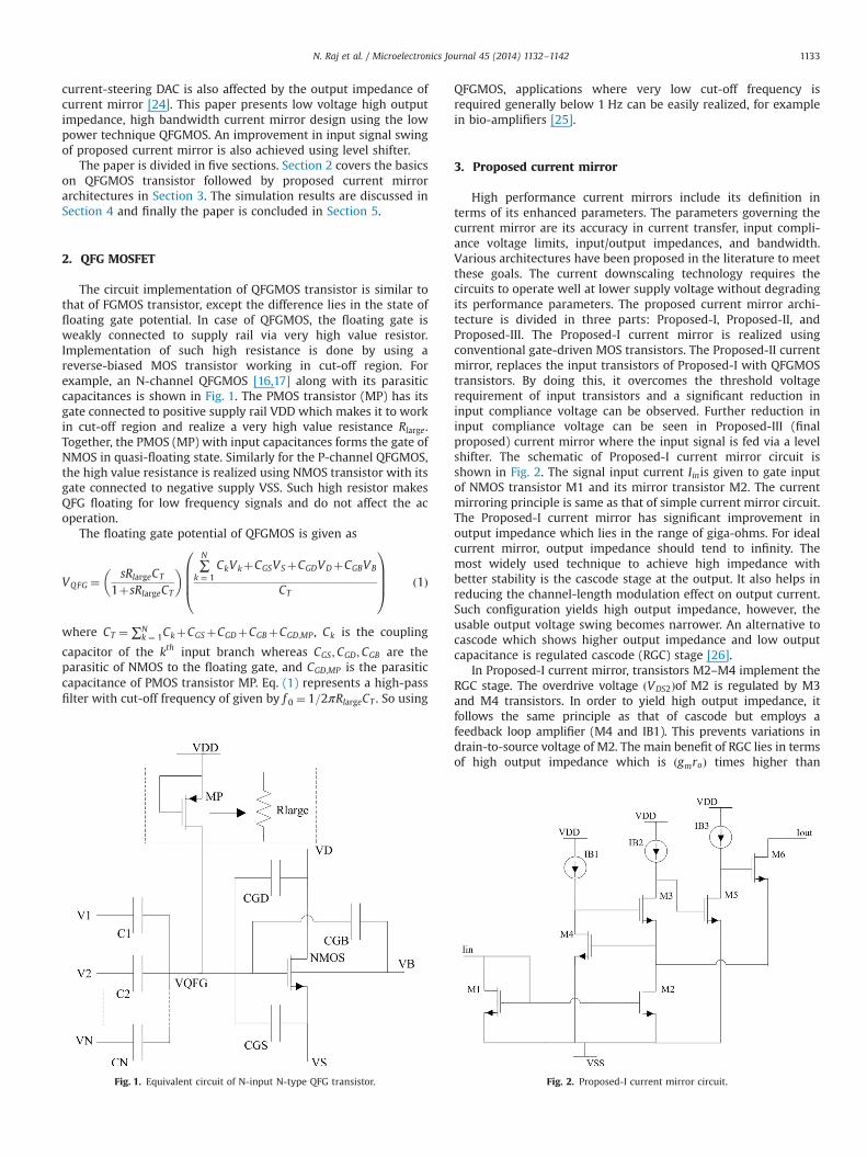
The circuit implementation of QFGMOS transistor is similar tothat of FGMOS transistor, except the difference lies in the state offloating gate potential. In case of QFGMOS, the floating gate isweakly connected to supply rail via very high value resistor.Implementation of such high resistance is done by using areverse-biased MOS transistor working in cut-off region. Forexample, an N-channel QFGMOS [16,17] along with its parasiticcapacitances is shown in Fig. 1. The PMOS transistor (MP) has itsgate connected to positive supply rail VDD which makes it to workin cut-off region and realize a very high value resistance Rlarge.Together, the PMOS (MP) with input capacitances forms the gate ofNMOS in quasi-floating state. Similarly for the P-channel QFGMOS,the high value resistance is realized using NMOS transistor with itsgate connected to negative supply VSS. Such high resistor makesQFG floating for low frequency signals and do not affect the acoperation.
The floating gate potential of QFGMOS is given as
VQFG ¼ sRlargeCT
1þsRlargeCT
� � ∑N
k ¼ 1CkVkþCGSVSþCGDVDþCGBVB
CT
0BBB@
1CCCA ð1Þ
where CT ¼∑Nk ¼ 1CkþCGSþCGDþCGBþCGD;MP , Ck is the coupling
capacitor of the kth input branch whereas CGS;CGD;CGB are theparasitic of NMOS to the floating gate, and CGD;MP is the parasiticcapacitance of PMOS transistor MP. Eq. (1) represents a high-passfilter with cut-off frequency of given by f 0 ¼ 1=2πRlargeCT . So using
QFGMOS, applications where very low cut-off frequency isrequired generally below 1 Hz can be easily realized, for examplein bio-amplifiers [25].
3. Proposed current mirror
High performance current mirrors include its definition interms of its enhanced parameters. The parameters governing thecurrent mirror are its accuracy in current transfer, input compli-ance voltage limits, input/output impedances, and bandwidth.Various architectures have been proposed in the literature to meetthese goals. The current downscaling technology requires thecircuits to operate well at lower supply voltage without degradingits performance parameters. The proposed current mirror archi-tecture is divided in three parts: Proposed-I, Proposed-II, andProposed-III. The Proposed-I current mirror is realized usingconventional gate-driven MOS transistors. The Proposed-II currentmirror, replaces the input transistors of Proposed-I with QFGMOStransistors. By doing this, it overcomes the threshold voltagerequirement of input transistors and a significant reduction ininput compliance voltage can be observed. Further reduction ininput compliance voltage can be seen in Proposed-III (finalproposed) current mirror where the input signal is fed via a levelshifter. The schematic of Proposed-I current mirror circuit isshown in Fig. 2. The signal input current Iinis given to gate inputof NMOS transistor M1 and its mirror transistor M2. The currentmirroring principle is same as that of simple current mirror circuit.The Proposed-I current mirror has significant improvement inoutput impedance which lies in the range of giga-ohms. For idealcurrent mirror, output impedance should tend to infinity. Themost widely used technique to achieve high impedance withbetter stability is the cascode stage at the output. It also helps inreducing the channel-length modulation effect on output current.Such configuration yields high output impedance, however, theusable output voltage swing becomes narrower. An alternative tocascode which shows higher output impedance and low outputcapacitance is regulated cascode (RGC) stage [26].
In Proposed-I current mirror, transistors M2–M4 implement theRGC stage. The overdrive voltage ðVDS2Þof M2 is regulated by M3and M4 transistors. In order to yield high output impedance, itfollows the same principle as that of cascode but employs afeedback loop amplifier (M4 and IB1). This prevents variations indrain-to-source voltage of M2. The main benefit of RGC lies in termsof high output impedance which is ðgmroÞ times higher than
Fig. 1. Equivalent circuit of N-input N-type QFG transistor. Fig. 2. Proposed-I current mirror circuit.
N. Raj et al. / Microelectronics Journal 45 (2014) 1132–1142 1133
conventional cascode stage. The capacitive current through Cgd3
which flows in biasing network is independent of current inputpath whereas in cascode this current appears twice. This reducedoutput capacitance improves the frequency response of the pro-posed current mirror. The output impedance is further enhanced byðgmroÞ2 using super cascode structure [27] realized using M5 andM6. The output transistor M6 of super cascode is driven by thedrain potential of M4 via the inverting amplifier realized by IB2 andM5. Using inverting amplifier stage provides the additional gain-boosting which further enhance the output impedance. The maindrawback in Proposed-I current mirror lies in low input signalswing. The input compliance voltage ðVinÞ of a current mirror is aparameter which decides the range of input voltage swing. The verycommon factor influencing input signal swing is the thresholdvoltage of input transistors which puts the limitation on inputcompliance voltage. To overcome the threshold voltage limitation,the widely acceptable QFGMOS technique is employed to the inputtransistors M1 and M2. The Proposed-II current mirror usingQFGMOS transistor as an input is shown in Fig. 3.
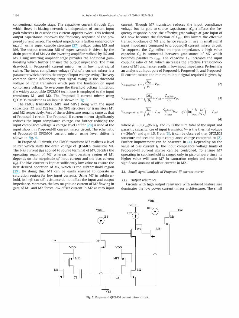
The PMOS transistors (MP1 and MP2) along with the inputcapacitors (C1 and C2) form the QFG structure for transistors M1and M2 respectively. Rest of the architecture remains same as thatof Proposed-I circuit. The Proposed-II current mirror significantlyreduces the input compliance voltage. For further reducing theinput compliance voltage, a voltage level shifter [28] is used at theinput shown in Proposed-III current mirror circuit. The schematicof Proposed-III QFGMOS current mirror using level shifter isshown in Fig. 4.
In Proposed-III circuit, the PMOS transistor M7 realizes a levelshifter which shifts the drain voltage of QFGMOS transistor M1.The bias current ðIBÞ applied to source terminal of M7, decides theoperating region of M7 whereas the operating region of M1depends on the magnitude of input current and the bias currentðIBÞ. The bias current is kept at sufficiently low value to ensure thebest desired operation of M7, which is the subthreshold region[29]. By doing this, M1 can be easily ensured to operate insaturation region for low input currents. Using M7 in subthres-hold, its high cut-off resistance do not affect the input and outputimpedance. Moreover, the lowmagnitude current of M7 flowing ingate of M1 and M2 forces low offset current in M2 at zero input
current. Though M7 transistor reduces the input compliancevoltage but its gate-to-source capacitance ðCgs7Þ affects the fre-quency response. Since, the effective gate voltage at gate input ofM1 now becomes the function of Cgs7, this lowers the effectivetransconductance of M1 and hence results in rise in small signalinput impedance compared to proposed-II current mirror circuit.To suppress the Cgs7 effect on input impedance, a high valuecapacitor CX is connected between gate-source of M7 whichbecomes parallel to Cgs7. The capacitor CX increases the inputcoupling ratio of M1 which increases the effective transconduc-tance of M1 and hence results in low input impedance. Performingan analysis at input port of Proposed-I, Proposed-II, and Proposed-III current mirror, the minimum input signal required is given by
Vin;proposed� I ¼ffiffiffiffiffiffiffiffi2Iinβ1
sþVth1 ð2Þ
Vin;proposed� II ¼ffiffiffiffiffiffiffiffi2Iinβ1
sþVth1�
Cgd;MP
CTVDD ð3Þ
Vin;proposed� III ¼ffiffiffiffiffiffiffiffi2Iinβ1
sþVth1�
Cgd;MP1
CTotalVDD�ηVT ln
IBIDO7
L7W7
� ���������� Vth7j
��ð4Þ
where β1 ¼ μnCoxðW=LÞ1 and CT is the sum total of the input andparasitic capacitances of input transistor, VT is the thermal voltageð � 26mVÞ and η¼ 1:5. From (3), it can be observed that QFGMOSstructure reduces the input compliance voltage compared to (2).Further improvement can be observed in (4). Depending on thevalue of bias current IB, the input compliance voltage limits ofProposed-III current mirror can be controlled. To ensure M7operating in subthreshold IB ranges only in pico-ampere since itshigher value will turn M7 in saturation region and results insignificant amount of offset current in M2.
3.1. Small signal analysis of Proposed-III current mirror
3.1.1. Output resistanceCircuits with high output resistance with reduced feature size
dominates the low power current mirror architectures. The small
Fig. 3. Proposed-II QFGMOS current mirror circuit.
N. Raj et al. / Microelectronics Journal 45 (2014) 1132–11421134

signal model for calculating the output resistance ðRoutÞ is shownin Fig. 5.
iout ¼ gm6V52þVout�V2
ro6ð5Þ
V2 ¼ ioutro2ð6Þ
and
V5 ¼ �ðgm5ro5Þðgm3ro3Þð1þgm4ro4ÞV2 ð7Þ
Fig. 4. Proposed-III QFGMOS current mirror circuit using level shifter.
Fig. 5. Small signal model for calculating output resistance.
Fig. 6. Small signal model for calculating bandwidth.
N. Raj et al. / Microelectronics Journal 45 (2014) 1132–1142 1135

From (5)–(7)
Rout ¼Vout
iout
¼ ðro6þro2ððgm6ro6Þðgm5ro5Þðgm3ro3Þð1þgm4ro4Þþð1þgm6ro6ÞÞÞð8Þ
Since gmro441
Rout � ro2ðgm3ro3Þðgm4ro4Þðgm5ro5Þðgm6ro6Þ ð9Þ
Table 1W and L of MOS transistors used in proposed CMs.
Transistors W (μm) L (μm) Transistors W (μm) L (μm)
M1 25 0.24 M6 5.33 0.24M2 25 0.24 M7 60 0.48M3 10 0.24 MP1 0.24 0.24M4 10 0.24 MP2 0.24 0.24M5 2.24 0.24
Cx¼5 pF, C1¼C2¼1 pF, supply¼70.5 V, IB¼10 pA, IB1¼30 μA, IB2¼ IB3¼100 μA.
Fig. 7. DC characteristics of Proposed-I, II, III for input current ranging from 100 μAto 700 μA.
Fig. 8. Current transfer characteristics of Proposed-I, II, III for input current rangingfrom 0 to 700 μA.
Fig. 9. Error in current transfer characteristics of Proposed-I, II, III current mirror.
Fig. 10. Input characteristics of Proposed-I, II, III current mirror.
Fig. 11. Frequency response for bandwidth calculation of Proposed-I, II, III currentmirror.
N. Raj et al. / Microelectronics Journal 45 (2014) 1132–11421136

From (9), an increment by ðgmroÞ4 times the output resistancecompared to conventional QFGMOS current mirror can be seenand which is almost in range of giga-ohms.
3.1.2. BandwidthThe frequency response of any analog circuits is function of its
gain and feedback capacitance. The small-signal model for calcu-lating bandwidth of Proposed-III current mirror is shown in Fig. 6.The symbols used in analysis matches with standard spice modelparameters of MOSFETs. Here, all the MOS transistors are assumedto be working in saturation region except M7 and MP which areworking in cut-off region. The output conductance is neglected.The Cgd effects are neglected in comparison to Cgs of saturationmode transistors. The capacitor CX connected in parallel to Cgs7 ofM7, reduces Cgs7 effect on input characteristic. The capacitors Cgd7
and Cgd;MP are the gate-to-drain capacitance of M7 and MPrespectively.
Fig. 12. Input resistance of Proposed-I, II, III current mirror.
Fig. 13. Output resistance of Proposed-I, II, III current mirror.
Table 2THD over varying input current signal amplitude at 10 MHz, 50 MHz, and 100 MHz for Proposed-I, II , III current mirror.
Amplitude of input signal μAð Þ THD for Proposed-I THD for Proposed-II THD for Proposed-III
10 MHz 50 MHz 100 MHz 10 MHz 50 MHz 100 MHz 10 MHz 50 MHz 100 MHz
10 0.035 1.024 1.002 0.084 1.040 1.038 0.076 1.113 1.23420 0.073 1.019 1.031 0.153 1.054 1.084 0.132 1.112 1.19030 0.084 1.028 1.044 0.201 1.096 1.148 0.168 1.145 1.22740 0.107 1.041 1.072 0.264 1.133 1.161 0.221 1.136 1.28150 0.129 1.056 1.097 0.332 1.173 1.212 0.276 1.176 1.33460 0.152 1.075 1.112 0.397 1.218 1.251 0.324 1.216 1.36670 0.176 1.093 1.137 0.436 1.264 1.303 0.387 1.260 1.42180 0.200 1.112 1.164 0.530 1.315 1.358 0.444 1.305 1.47790 0.224 1.133 1.193 0.598 1.367 1.415 0.501 1.353 1.536
100 0.249 1.157 1.223 0.668 1.425 1.475 0.560 1.410 1.599110 0.275 1.179 1.256 0.739 1.482 1.537 0.619 1.463 1.666120 0.302 1.203 1.291 0.814 1.541 1.603 0.683 1.520 1.738130 0.330 1.230 1.328 0.889 1.604 1.670 0.747 1.576 1.813140 0.359 1.256 1.369 0.968 1.667 1.741 0.813 1.640 1.894150 0.389 1.286 1.413 1.049 1.737 1.819 0.883 1.709 1.983160 0.421 1.317 1.462 1.134 1.809 1.899 0.958 1.779 2.077170 0.455 1.353 1.519 1.222 1.886 1.988 1.033 1.856 2.174180 0.490 1.391 1.580 1.315 1.968 2.080 1.112 1.939 2.292190 0.528 1.395 1.650 1.413 1.989 2.179 1.196 1.997 2.420200 0.569 1.434 1.731 1.518 2.121 2.288 1.287 2.070 2.563210 0.613 1.488 1.801 1.630 2.227 2.408 1.385 2.183 2.731220 0.663 1.496 1.834 1.753 2.348 2.498 1.490 2.238 2.821230 0.719 1.563 1.898 1.887 2.474 2.564 1.607 2.377 2.930240 0.791 1.628 2.224 2.039 2.642 2.837 1.738 2.552 3.379
Fig. 14. THD plot for Proposed-I, II, III current mirror for 10 MHz input sinusoidalsignal.
N. Raj et al. / Microelectronics Journal 45 (2014) 1132–1142 1137

At input node 9,
iin ¼ gm1V7þsCAV7 ð10Þ
where
CA ¼ 2C1;2 J ðCgs1;2þCgd;MP1;2Þ
þCgd7ð2C1;2 J ðCgs1;2þCgd;MP1;2ÞþCXþCgs7ÞCXþCgs7
At output node 4,
iout ¼ gm2gm3gm4
gm4ðgm3þsCgs3Þþs2Cgs3Cgs4V7 ð11Þ
From (10) and (11),
AI ¼ioutiin
¼ gm2gm3gm4
Cgs3Cgs4CAðsþðgm1=CAÞÞðs2þðgm4=Cgs4Þsþðgm3gm4=Cgs3Cgs4ÞÞð12Þ
The mid-band gain at s¼0 is
ioutiin
¼ gm2gm3gm4
gm1gm3gm4¼ gm2
gm1
same as that of simple current mirror
Solving for roots of (12),
P1 ¼ �gm1
CAð13Þ
P2;3 ¼�ðgm4=Cgs4Þ7
ffiffiffiffiffiffiffiffiffiffiffiffiffiffiffiffiffiffiffiffiffiffiffiffiffiffiffiffiffiffiffiffiffiffiffiffiffiffiffiffiffiffiffiffiffiffiffiffiffiffiffiffiffiffiffiffiffiffiffiffiffiffiffiffiffiffiffiffiffiffiðgm4=Cgs4Þ2�4ðgm3gm4=Cgs3Cgs4Þ
q2
ð14Þ
The proposed current mirror have one real pole and twocomplex poles. The dominant pole P1 determines the bandwidthof current mirror which lies in the order of giga hertz.
4. Simulation results
The proposed current mirror circuit's shown in Figs. 2–4 hasbeen simulated on 0.18 μm mixed-mode twin-well technology
Fig. 15. THD plot for Proposed-I, II, III current mirror for 50 MHz input sinusoidalsignal.
Fig. 16. THD plot for Proposed-I, II, III current mirror for 100 MHz input sinusoidalsignal.
Table 3Output current vs input current variation for different process corner with theircurrent matching error ratio ðIout� IinÞ=Iin .
Input current(μA)
Output current (μA) for (%) Current matching errorration for
Typicalcorner
Fastcorner
Slowcorner
Typicalcorner
Fastcorner
Slowcorner
50 50.500 54.100 46.416 0.01 0.08 �0.07100 105.077 111.164 98.445 0.05 0.11 �0.01150 157.598 165.829 148.960 0.05 0.10 �0.006200 208.874 219.009 198.579 0.04 0.09 �0.007250 259.291 271.143 247.588 0.03 0.08 �0.009300 309.067 322.487 296.147 0.03 0.07 �0.01350 358.339 373.207 344.352 0.02 0.06 �0.01400 407.204 423.415 392.268 0.01 0.05 �0.01450 455.726 473.194 439.941 0.01 0.05 �0.02500 503.956 522.603 487.402 0.007 0.04 �0.02550 551.931 571.690 534.677 0.003 0.03 �0.02600 599.682 620.493 581.781 �0.00 0.03 �0.03650 647.230 669.041 628.732 �0.00 0.02 �0.03700 694.595 717.358 675.536 �0.00 0.02 �0.03
Fig. 17. Error in current transfer characteristic of Proposed-III current mirror atTypical, Fast, and Slow process corners.
N. Raj et al. / Microelectronics Journal 45 (2014) 1132–11421138

provided by UMC using 70.5 V supply with the help of HSpicesimulator. The simulations confirm excellent properties of pro-posed current mirror circuits. The device dimension of transistorsused in proposed-I, II, and III current mirror is shown in Table 1.The other assumed parameters for circuit simulations are alsolisted in Table 1. The selection of input bias currents is to ensurelower Vin and offset in the circuit. The input dc bias current is keptat 65 μA. The channel length of the transistors is kept at itsminimum value.
In Fig. 7, the output current is plotted in relation to outputvoltage for input current values ranging from 100 μA to 700 μA insteps of 100 μA. It has been observed that among the proposedcurrent mirror circuits, Proposed-III copy the input current withminimal offset. The current transfer characteristics of Proposed-I,II, and III circuits from 0 to 700 μA is shown in Fig. 8 andcorresponding the current copying accuracy error percentage isshown in Fig. 9.
The minimum error percentage in current transfer ratio can beobserved for Proposed-III current mirror which varies from 1% (forinput currents below 100 μA) to 5% (for input currents above100 μA) and further decreases for high input current.
The input characteristic of proposed current mirrors over inputcurrent ranging from 0 to 700 μA is shown in Fig. 10. The inputcompliance voltage range of Proposed-II is found to be lower thanthe proposed-I by 230 mV at 700 μA which is further reduced by100 mV in Proposed-III current mirror with the help of levelshifter technique. The frequency response of the Proposed-I, II,and III current mirror is shown in Fig. 11.
The graph for input impedance of proposed current mirrorcircuits is shown in Fig. 12. The effect of using Cx in gaining thehigher transconductance of M1 can be observed in input impe-dance plot where the impedance achieved by Proposed-IIIbecomes almost equal to Proposed-II current mirror. The outputimpedance plot is shown in Fig. 13.
For non-linearity analysis of Proposed-I, II, and III currentmirror, the transient analysis is performed for evaluating the totalharmonic distortion (THD) for input current wave sine signal atfrequency of 10 MHz, 50 MHz and 100 MHz for a quiescent currentof 250 μA. The THD percentage at above stated frequencies istabulated in Table 2 and results are plotted in Figs. 14–16. It isfound that with increase in input signal amplitude and frequencythere is increase in THD percentage.
Fig. 19. Monte Carlo (100 runs) analysis for Iout at Iin¼0 to 700 μA applying 5%channel length variation on Proposed-III current mirror.
Fig. 20. Monte Carlo (100 runs) analysis for Vin at Iin¼0 to 700 μA applying 5%channel length variation on Proposed-III current mirror.
Fig. 18. Monte Carlo (100 runs) analysis for Iout/Vout at Iin¼700 μA applying 5%channel length variation on Proposed-III current mirror.
Fig. 21. Monte Carlo (100 runs) analysis for input resistance applying 5% channellength variation on Proposed-III current mirror.
N. Raj et al. / Microelectronics Journal 45 (2014) 1132–1142 1139

In industry, the MOS transistor fabrication suffers process andenvironmental variations from wafer to wafer. The robustness offinal Proposed-III current mirror circuit is shown by simulating it
on three different process corners, namely Typical, Fast, and Slow.The output current variation to input current at these corners withtheir current matching error ratio is tabulated in Table 3 and
Fig. 22. Monte Carlo (100 runs) analysis for output resistance applying 5% channellength variation on Proposed-III current mirror.
Fig. 23. Monte Carlo (100 runs) analysis for bandwidth calculation applying 5%channel length variation on Proposed-III current mirror.
Table 4Output current vs input current variation for temperatures with their current matching error ratio ðIout� IinÞ=Iin .
Input Current ðμAÞ Output current ðμAÞ for Typical corner Current matching error ratio for Typical corner
�251C 01C þ251C þ501C þ751C �251C 01C þ251C þ501C þ751C
50 55.204 53.413 50.500 50.360 48.995 0.10 0.06 0.01 0.007 �0.02100 111.155 107.890 105.077 102.367 99.922 0.11 0.07 0.05 0.02 �0.007150 165.296 160.810 157.598 153.172 149.788 0.10 0.07 0.05 0.02 �0.001200 218.300 212.761 208.874 203.252 199.021 0.09 0.06 0.04 0.01 �0.004250 270.506 264.034 259.291 252.825 247.813 0.08 0.05 0.03 0.01 �0.008300 322.117 314.798 309.067 302.019 296.274 0.07 0.04 0.03 0.006 �0.01350 373.264 365.164 358.339 350.909 344.468 0.06 0.04 0.02 0.002 �0.01400 424.034 415.205 407.204 399.551 392.440 0.06 0.03 0.01 �0.001 �0.01450 474.494 464.975 455.726 447.979 440.221 0.05 0.03 0.01 �0.004 �0.02500 524.691 514.514 503.956 496.222 487.832 0.04 0.02 0.007 �0.007 �0.02550 574.660 563.852 551.931 544.300 535.290 0.04 0.02 0.003 �0.01 �0.02600 624.431 613.012 599.682 592.229 582.607 0.04 0.02 �0.00 �0.01 �0.02650 674.026 662.013 647.230 640.021 629.793 0.03 0.01 �0.00 �0.01 �0.03700 723.464 710.871 694.595 687.685 676.855 0.03 0.01 �0.00 �0.01 �0.03
Fig. 24. Temperature analysis for current matching error ratio at �251C, 01C,þ251C, þ501C and þ751C.
Fig. 25. Temperature analysis for Iout/Vout at Iin¼700 μA from�251C to þ751C atthe steps of þ251C.
N. Raj et al. / Microelectronics Journal 45 (2014) 1132–11421140

corresponding plot appears in Fig. 17. It can be observed that theProposed-III current mirror operates within acceptable range inwhole design space.
Any circuit must meet tolerances for the specific manufacturingprocess for maximum process yield. Such analyses are used tomodify DC operating points, DC sweeps, AC sweeps, and transientanalysis. The model parameter like channel length of MOS tran-sistor varies from transistor to transistor by a small amountdepending on the die distribution which is supposed to be amajor cause for offsets and mismatch in the analog circuits. Theanalysis of such parameter variations of transistors used inProposed-III current mirror circuit is shown by applying 5%mismatch with the help of Gaussian distribution. Using MonteCarlo simulations (100 runs), the mismatch effects of channellength on performance characteristics of Proposed-III circuit isshown in Figs. 18–23. From these graphs, it can be observed thatthe fabrication process does not have significant effect on pro-posed current mirror performance.
Further to verify the performance of the proposed currentmirror against PVT (process, VDD and temperature) varia-tions, the basic characteristics of current mirror are plotted onvarious temperatures. The current matching error ratio for typicalcorner at various temperatures is tabulated in Table 4 andthe corresponding plot is shown in Fig. 24. The output andinput characteristics, and frequency response for temperaturesranging from �251C to þ751C at the steps of þ251C are shown inFigs. 25–27.
Further, to evaluate the performance a comparative analysis ofProposed-I, II, and III current mirror with existing gate driven,FGMOS and QFGMOS based current mirror is shown in Table 5.From Table 5, it can be concluded that the proposed currentmirrors has wide operating range maintaining the same powerconsumption level. The achieved input/output impedance andhigh bandwidth without using any compensation techniqueencourages its application for low power designs.
5. Conclusion
The paper presents a low-voltage QFGMOS based currentmirror. The attractive parameters of proposed current mirror areits wide operating range, low input compliance voltage, and highoutput impedance. The achieved giga-hertz bandwidth makes itattractive for high frequency analog circuits, required in signal-processing applications. The proposed current mirror consumespower less than 1 mW. The validation of characteristics of pro-posed current mirror has been done with industry specifictechnology through the standard HSpice simulator.
Fig. 26. Temperature analysis for Vin at Iin¼0 to 700 μA from �251C to þ751C atthe steps of þ251C.
Fig. 27. Temperature analysis for current gain in dB from �251C to þ751C at thesteps of þ251C.
Table 5Comparative study on Current Mirror performance parameters with Proposed-I, II, and III current mirror.
Parameters Ref.
[7] [12] [21] [30] Proposed-I Proposed-II Proposed-III
Input current range ðμAÞ 0.1–500 0–500 0–500 0–500 0–700 0–700 0–700Input resistance (Ω) NA 1.1K 235 679 265 140 160Output resistance (Ω) 1.35 M 143.4 K 117 K 482 M 12.9 G 8.05 G 8.55 GInput compliance voltage (V) NA 0.41@50 μA 0.2@500 μA NA 0.68@500 μA 0.34@500 μA 0.26@500 μA
0.64@700 μA 0.41@700 μA 0.31@700 μABWðHzÞ 500 M 1.2 G 1.52 G 2.26 G 3.65 G 4.2 G 4.05 GPower (W) NA 1.13 m 0.83 m NA 0.887 m 0.821 m 0.841 mInput bias current ðμAÞ NA 500 NA NA 65 65 65Supply (V) 70.65 70.75 70.5 �1 70.5 70.5 70.5Technology 0.25 μm 0.5 μm 0.13 μm TSMC UMC UMC UMC
0.18 μm 0.18 μm 0.18 μm 0.18 μm
N. Raj et al. / Microelectronics Journal 45 (2014) 1132–1142 1141

References
[1] J. Ramirez-Angulo, C. Urquidi, R.G. Carvajal, A. Lopez-Martin, A new family oflow-voltage analog circuits based on quasi floating gate transistors, IEEE Trans.on Circuits Syst.-II 50 (5) (2003) 214–220, http://dx.doi.org/10.1109/TCSII.2003.811434.
[2] J. Ramirez-Angulo, S.C. Choi, G. Gonzalez-Altamiran, Low supply voltage OTAarchitectures using floating gate transistors, IEEE Trans. Circuits Syst. 442 (12)(1995) 971–974, http://dx.doi.org/10.1109/MWSCAS.1995.504402.
[3] J. Ramirez-Angulo, R.G. Carvajal, J. Tombs, A. Torralba, Low-voltage CMOS op-amp with rail-to-rail input and output signal swing for continuous-time signalprocessing using multiple-input floating-gate transistors, IEEE Trans. CircuitsSyst.-II: Analog Digit. Signal Process. 48 (1) (2001) 111–116, http://dx.doi.org/10.1109/82.913195.
[4] E. Rodriguez-Villegas, M. Jimenez, R.G. Carvajal, On dealing with the chargetrapped in Floating-Gate MOS (FGMOS) transistors, IEEE Trans. Circuits Syst.-II: Express Briefs 54 (2) (2007) 156–160, http://dx.doi.org/10.1109/TCSII.2006.886226.
[5] W.P., Millard , Z.K. , Kalyjian, A.G. , Andreou ‘Calibration and matching offloating gate devices,’ in: Proceedings of the 2000 IEEE International Sympo-sium on Circuits and Systems, (ISCAS), Geneva, vol. 4, 2000, pp. 389–392.(http://dx.doi.org/10.1109/ISCAS.2000.858770).
[6] S., Sharma, S.S., Rajput, L.K., Magotra, S.S. , Jamuar, ‘FGMOS based wide rangelow voltage current mirror and its applications,’ in: Proceeding of the Asia-Pacific Conference on Circuits and Systems, (APCCAS ‘02), vol.2, 2002, pp. 331–334. (http://dx.doi.org/10.1109/APCCAS.2002.1115251).
[7] S. Yan, E. Sanchez-Sinencio, Low voltage analog circuit design: a tutorial, IEICETrans. Analog Integr. Circuits Syst. vol. E83A (2) (2000) 179–196.
[8] J. Ramirez-Angulo, A.J. Lopez, MITE circuits: the continuous-time counterpartto switched-capacitor circuits, IEEE Trans. Circuits Syst. II: Analog Digit. SignalProcess. 48 (1) (2001) 45–55, http://dx.doi.org/10.1109/82.913186.
[9] M. Gupta, R. Pandey, Low-voltage FGMOS based analog building blocks,Microelectron. J. 42 (6) (2011) 903–912, http://dx.doi.org/10.1016/j.mejo.2011.03.013.
[10] J., De la Cruz Alejo, L.N.O., Moreno, ‘Mismatch compensation in currentmirrors with FGMOS transistor,’ in: Proceedings of the 7th InternationalConference on Electrical Engineering Computing Science and AutomaticControl (CCE), 2010, pp. 599–603. (http://dx.doi.org/10.1109/ICEEE.2010.5608617).
[11] S. Sharma, S.S. Rajput, L.K. Mangotra, S.S. Jamuar, FGMOS current mirror:behaviour and bandwidth enhancement, Analog Integr. Circuits Signal Process.46 (3) (2006) 281–286, http://dx.doi.org/10.1007/s10470-006-1625-6.
[12] S.S., Rajput, S.S.,Jamuar, ‘Advanced current mirrors for low voltage analogdesigns,’ in: Proceedings of the IEEE International Conference on Semicon-ductor Electronics, 2004, pp. 258–263. (http://dx.doi.org/10.1109/SMELEC.2004.1620882).
[13] B.Aggarwal, , M., Gupta, ‘Low-Voltage Cascode Current Mirror Based on Bulk-Driven MOSFET and FGMOS Techniques,’ in: Proceedings of the InternationalConference on Advances in Recent Technologies in Communication andComputing (ARTCom'09), Oct. 2009, pp. 473–477. (http://dx.doi.org/10.1109/ARTCom.2009.83).
[14] K. Ahlad, Split length FGMOS MOS cell: a new block for low voltageapplications, Analog Integr. Circuits Signal Process. 75 (3) (June 2013)399–405, http://dx.doi.org/10.1007/s10470-012-0001-y.
[15] J. Ramirez-Angulo, A.J. Lopez-Martin, R. Gonzalez-Carvajal, F. Munoz Chavero,Very low voltage analog signal processing based on quasi floating gatetransistors, IEEE J. Solid State Circuits 39 (2004) 434–442, http://dx.doi.org/10.1109/JSSC.2003.822782.
[16] J.M.A. Miguel, A.J. Lopez-Martin, L. Acosta, J. Ramirez-Angulo, R.G. Carvajal,Using floating gate and quasi-floating gate techniques for rail-to-rail tunableCMOS transconductor design, IEEE Trans. on Circuits Syst. I: Regul. Pap 58 (7)(2011) 1604–1614, http://dx.doi.org/10.1109/TCSI.2011.2157782.
[17] A. Torralba, C. Luja n-Martinez, R.G. Carvajal, J. Galan, M. Pennisi, J. Ramirez-Angulo, A. Lopez-Martin, Tunable linear MOS resistors using quasi-floating-gate techniques, IEEE Trans. on Circuits Syst. II: Express Briefs 56 (no. 1) (2009)41–45, http://dx.doi.org/10.1109/TCSII.2008.2010163.
[18] C. Garcia-Alberdi, A. Lopez-Martin, L. Acosta, R.G. Carvajal, J. Ramirez-Angulo,‘Tunable class AB CMOS Gm-C filter based on quasi-floating gate techniques,',IEEE Trans. on Circuits Syst. I: Regul. Pap. 60 (5) (2013) 1300–1309, http://dx.doi.org/10.1109/TCSI.2012.2220504.
[19] H. Moradzadeh, S.J. Azhari, Low-voltage low-power rail-to-rail low-Rx wide-band second generation current conveyor and a single resistance-controlledoscillator based on it, IET Circuits Devices Syst. 5 (1) (2011) 66–72, http://dx.doi.org/10.1049/iet-cds.2010.0178.
[20] R. Gupta, S. Sharma, Quasi-floating gate MOSFET based low voltage currentmirror, Microelectron. J. 43 (7) (2012) 439–443, http://dx.doi.org/10.1016/j.mejo.2012.04.006.
[21] N. Raj, A.K. Singh, A.K. Gupta, Low-voltage bulk-driven self-biased cascodecurrent mirror with bandwidth enhancement, Electron. Lett. 50 (1) (2014)23–25, http://dx.doi.org/10.1049/el.2013.3600.
[22] R. Gupta, S. Sharma, Voltage controlled resistor using quasi-floating-gateMOSFETs, Maejo Int. J. Sci. Technol. 7 (01) (2013) 16–25.
[23] P.E. Allen, D.R. Holberg, CMOS Analog Circuit Design, Second edition, OxfordUniversity Press, USA, 2002.
[24] S.J. Azhari, K. Monfaredi, S. Amiri, A 12-bit, low-voltage, nanoampere-based,ultralow-power, ultralow-glitch current-steering DAC for HDTV, Int. Nano Lett.2 (1) (2012) 1–7, http://dx.doi.org/10.1186/2228-5326-2-35.
[25] R.R., Harrison, ‘A low-power, low-noise CMOS amplifier for neural recordingapplications,’ in: Proceedings of the IEEE International Symposium on Circuitsand Systems (ISCAS'02), 2002, vol.5, pp. v197–v200. (http://dx.doi.org/10.1109/ISCAS.2002.1010674).
[26] E. Sackinger, W. Guggenbuhl, A high-swing, high-impedance MOS cascodecircuit, IEEE J. Solid State Circuits 25 (1) (1990) 289–298, http://dx.doi.org/10.1109/4.50316.
[27] A. Torralba, R.G. Carvajal, J. Ramirez-Angulo, E. Munoz, Output stage for lowsupply voltage high-performance CMOS current mirrors, Electron. Lett. 38 (24)(2002) 1528–1529, http://dx.doi.org/10.1049/el:20021062.
[28] V.I. Prodanov, M.M. Green, CMOS current mirrors with reduced input andoutput voltage requirements, Electron. Lett. 32 (2) (1996) 104–105, http://dx.doi.org/10.1049/el:19960076.
[29] S.S. Rajput, S.S. Jamuar, A current mirror for low voltage, high performanceanalog circuits, Analog Integr. Circuits Signal Process. 36 (2003) 221–233,http://dx.doi.org/10.1023/A:1024718421282.
[30] M. Gupta, B. Aggarwal, A.K. Gupta, A very high performance self-biasedcascode current mirror for CMOS technology, Analog Integr. Circuits SignalProcess. 75 (1) (2013) 67–74, http://dx.doi.org/10.1007/s10470-012-9994-5.
N. Raj et al. / Microelectronics Journal 45 (2014) 1132–11421142