Linear Modelling - CORE
84
Universidade de Aveiro 2016 Departamento de Eletrónica, Telecomunicações e Informática Cristiano Ferreira Gonçalves Caracterização de Transístores GaN HEMT para Modelação Não Linear GaN HEMT Transistors Characterization for Non– Linear Modelling
-
Upload
khangminh22 -
Category
Documents
-
view
2 -
download
0
Transcript of Linear Modelling - CORE

Universidade de Aveiro
2016
Departamento de Eletrónica, Telecomunicações e Informática
Cristiano Ferreira Gonçalves
Caracterização de Transístores GaN HEMT para Modelação Não Linear GaN HEMT Transistors Characterization for Non–Linear Modelling


Universidade de Aveiro
2015
Departamento de Eletrónica, Telecomunicações e Informática
Cristiano Ferreira Gonçalves
Caracterização de Transístores GaN HEMT para Modelação Não Linear GaN HEMT Transistors Characterization for Non–Linear Modelling
Dissertação apresentada à Universidade de Aveiro para cumprimento dos requisitos necessários à obtenção do grau de Mestre em Engenharia Eletrónica e Telecomunicações, realizada sob a orientação científica do Doutor José Carlos Esteves Duarte Pedro, Professor Catedrático do Departamento de Eletrónica, Telecomunicações e Informática da Universidade de Aveiro e sob a coorientação científica do Doutor Pedro Miguel da Silva Cabral, Professor auxiliar do Departamento de Eletrónica, Telecomunicações e Informática da Universidade de Aveiro. Dissertation presented to the university of Aveiro for the fulfillment of the necessary requisites to obtain the degree of Master in Electronics and Telecommunication Engineering, developed under the scientific guidance of Doctor José Carlos Esteves Duarte Pedro, full professor of the Electronics, Telecommunications and Informatics Department of the University of Aveiro and Doctor Pedro Miguel da Silva Cabral associated professor of the Electronics, Telecommunications and Informatics Department of the University of Aveiro.

Dedico este trabalho aos meus pais e às minhas irmãs por todo o apoio que me proporcionaram. Aos meus amigos, também, pelos momentos de distração necessários.


O júri / The jury
Presidente / President Prof. Doutor João Nuno Pimentel da Silva Matos Professor Associado da Universidade de Aveiro
Arguente Principal / Main Examiner Prof. Doutor João José Lopes da Costa Freire Professor Associado com Agregação da Universidade de Lisboa
Orientador / Advisor Prof. Doutor José Carlos Esteves Duarte Pedro Professor Catedrático da Universidade de Aveiro


Agradecimentos / Acknowledgments
É com toda a sinceridade que agradeço aos meus pais por me terem possibilitado a oportunidade de iniciar e percorrer todo este percurso académico. Tenho a plena noção que sem o esforço e dedicação deles isto também não seria possível.
Agradeço também ao meu orientador e professor José Carlos Esteves Duarte Pedro, tal como ao meu co-orientador Pedro Miguel da Silva Cabral por todo o conhecimento transmitido e tempo disponibilizado ao longo dos últimos meses.
Ao Doutor Francesc Martin Purroy, toda a sua equipa, e em especial ao Doutor Luis Carlos Cótimos Nunes por toda a sua ajuda, conhecimento transmitido, disponibilidade e profissionalismo durante todas as etapas deste trabalho.
À Universidade de Aveiro e Instituto de Telecomunicações pela disponibilização de todos os espaços, equipamentos e laboratórios.
À Huawei Technologies Sweden AB pela disponibilização dos seus laboratórios e equipamentos, os quais foram muito importantes para a realização de todo o trabalho.
Por último, a todos os meus colegas, pelo seu apoio, não só nesta fase mas durante todo o meu percurso académico.

Palavras-Chave
Amplificador de Potencia RF, Caracterização, Colapso da Currente, Curvas IV Pulsadas, GaN HEMT, Linearidade, Modelação, Parametros S Pulsados, Pulser, Transistor de RF.
Resumo
Ultimamente, as redes de telecomunicações móveis estão a exigir cada vez maiores taxas de transferência de informação. Com este aumento, embora sejam usados códigos poderosos, também aumenta a largura de banda dos sinais a transmitir, bem como a sua frequência. A maior frequência de operação, bem como a procura por sistemas mais eficientes, tem exigido progressos no que toca aos transístores utilizados nos amplificadores de potência de radio frequência (RF), uma vez que estes são componentes dominantes no rendimento de uma estação base de telecomunicações. Com esta evolução, surgem novas tecnologias de transístores, como os GaN HEMT (do inglês, Gallium Nitride High Electron Mobility Transistor). Para conseguir prever e corrigir certos efeitos dispersivos que afetam estas novas tecnologias e para obter o amplificador mais eficiente para cada transístor usado, os projetistas de amplificadores necessitam cada vez mais de um modelo que reproduza fielmente o comportamento do dispositivo. Durante este trabalho foi desenvolvido um sistema capaz de efetuar medidas pulsadas e de elevada exatidão a transístores, para que estes não sejam afetados, durante as medidas, por fenómenos de sobreaquecimento ou outro tipo de fenómenos dispersivos mais complexos presentes em algumas tecnologias. Desta forma, será possível caracterizar estes transístores para um estado pré determinado não só de temperatura, mas de todos os fenómenos presentes. Ao longo do trabalho vai ser demostrado o projeto e a construção deste sistema, incluindo a parte de potência que será o principal foco do trabalho. Foi assim possível efetuar medidas pulsadas DC-IV e de parâmetros S (do inglês, Scattering) pulsados para vários pontos de polarização. Estas últimas foram conseguidas á custa da realização de um kit de calibração TRL. O interface gráfico com o sistema foi feito em Matlab, o que torna o sistema mais fácil de operar. Com as medidas resultantes pôde ser obtida uma primeira análise acerca da eficiência, ganho e potência máxima entregue pelo dispositivo. Mais tarde, com as mesmas medidas pôde ser obtido um modelo não linear completo do dispositivo, facilitando assim o projeto de amplificadores.


Keywords
Characterization, Current Collapse, Gan HEMT, Linearity, Modeling, Pulsed IV, Pulsed S-Parameters, Pulser Head, RF Power Amplifier, RF Transistor.
Abstract
Lately, the wireless networks should feature higher data rates than ever. With this rise, although very powerful codification schemes are used, the bandwidth of the transmitted signals is rising, as well as the frequency. Not only caused by this rise in frequency, but also by the growing need for more efficient systems, major advances have been made in terms of Radio Frequency (RF) Transistors that are used in Power Amplifiers (PAs), which are dominant components in terms of the total efficiency of base stations (BSS). With this evolution, new technologies of transistors are being developed, such as the Gallium Nitride High Electron Mobility Transistor (GaN HEMT). In order to predict and correct some dispersive effects that affect these new technologies and obtain the best possible amplifier for each different transistor, the designers are relying more than ever in the models of the devices. During this work, one system capable of performing very precise pulsed measurements on RF transistors was developed, so that they are not affected, during the measurements, by self-heating or other dispersive phenomena that are present in some technologies. Using these measurements it was possible to characterize these transistors for a pre-determined state of the temperature and all the other phenomena. In this document, the design and assembly of the complete system will be analysed, with special attention to the higher power component. It will be possible to measure pulsed Direct Current Current-Voltage (DC-IV) behaviour and pulsed Scattering (S) parameters of the device for many different bias points. These latter ones were possible due to the development of one TRL calibration kit. The interface with the system is made using a graphical interface designed in Matlab, which makes it easier to use. With the resulting measurements, as a first step analysis, the maximum efficiency, gain and maximum delivered power of the device can be estimated. Later, with the same measurements, the complete non-linear model of the device can be obtained, allowing the designers to produce state-of-art RF PAs.


i
Table of Contents
TABLE OF CONTENTS .................................................................................................. I
LIST OF FIGURES ...................................................................................................... III
LIST OF TABLES ......................................................................................................... V
LIST OF ACRONYMS .................................................................................................. 7
1. INTRODUCTION ................................................................................................ 9
1.1. Inherent Problems in GaN Devices .................................................................................. 9
1.2. Pulsed Measurement Systems ....................................................................................... 11
1.3. Objectives ......................................................................................................................... 13
1.4. Different Available Solutions .......................................................................................... 15
1.5. Summary ........................................................................................................................... 16
2. DESIGN AND IMPLEMENTATION OF A POWER PULSER HEAD ............................... 19
2.1. Design of the Circuit ........................................................................................................ 19
2.2. Design and Implementation of the Board ...................................................................... 25
2.3. Validation and Test .......................................................................................................... 26
3. DC-IV CHARACTERIZATION OF A RADIO FREQUENCY TRANSISTOR .................... 33
3.1. Inherent Problems and Used Technics During the Characterization ......................... 33
3.2. Analysis of the Obtained Results ................................................................................... 42
4. IV CHARACTERIZATION AND SMALL SIGNAL ANALYSIS COMPARISON .................. 47
4.1. S-Parameter Measurements ........................................................................................... 47
4.2. Transcondutance (gm) and Output Conductance (gds) Deduction and Integration 51
4.3. Validation of the Pulsed Measurement System ............................................................ 54

ii
5. CONCLUSION AND FUTURE WORK ................................................................... 61
5.1. Conclusion ....................................................................................................................... 61
5.2. Future Work ...................................................................................................................... 62
6. REFERENCES ................................................................................................ 65
7. APPENDICES .................................................................................................. 67
7.1. Appendix A – TRL Calibration Kit Description ............................................................. 67

iii
List of Figures
Figure 1 – Basic GaN layer structure and in package pre matched GaN chip. ........................................ 10 Figure 2 – Equivalent model of one MESFET, ‘im’ defined in equation (1). ............................................. 12 Figure 3 – Example of a DC-IV behaviour pulsed measurement. ............................................................ 13 Figure 4 – Photographs of the pulsed measurement systems, AURIGA’s one on the left, and AMCAD on
the right. ................................................................................................................................. 16 Figure 5 – Example of a generic voltage-series feedback system. .......................................................... 20 Figure 6 – Pulser simplified SPICE-like schematic. ................................................................................. 21 Figure 7 – Small signal asymmetrical voltage source, featuring switchable resistor. ............................... 23 Figure 8 – Dissipated power on the Pulser, for 130 V supply voltage. ..................................................... 24 Figure 9 – Delivered power of the Pulser, for 130 V supply voltage. ........................................................ 24 Figure 10 – Top layer drawing of the Pulser PCB. ................................................................................... 25 Figure 11 – Photograph of the Pulser after fully assembled. ................................................................... 26 Figure 12 – Loads used to characterize the Pulser. ................................................................................. 27 Figure 13 – Comparison between HB simulations and transient ones. .................................................... 27 Figure 14 – Calculated approximation error (difference between simulations). ....................................... 27 Figure 15 – Comparison between simulations and measurements, for the 50 Ω load. ............................ 28 Figure 16 – Comparison between simulations and measurements, for the 4 Ω load. .............................. 28 Figure 17 – Simulated response of the Pulser with one capacitive load of 10 nF, on the left, and one
equation defined load that simulates the behavior of one Transistor, on the right. ................ 29 Figure 18 – 2.5 Ω test load, used for high peak power tests. ................................................................... 29 Figure 19 – Results of the high power test performed in the previous shown load. ................................. 30 Figure 20 - Results of the characterization of a 220 W RF device. .......................................................... 30 Figure 21 – Example of the average settling time obtained with the Pulser. ............................................ 31 Figure 22 – Simplified RC physical Cauer Network model of the warming and cooling of any device. .... 34 Figure 23 – Very first used signal, 10 us of width. .................................................................................... 34 Figure 24 – First test setup used to characterize the device. ................................................................... 35 Figure 25 – Required signal shaping. ...................................................................................................... 36 Figure 26 – Example of one 𝑣𝐷𝑆 and 𝑖𝐷𝑆 pulse. ....................................................................................... 36 Figure 27 – First DC-IV characteristic curves, measured for the 15 W Cree GaN. .................................. 36 Figure 28 – Schematic of one GaN HEMT including the analysis of the virtual gate created. ................. 37 Figure 29 – Schematic of one GaN HEMT where the positive charges are shown, trapped in the Buffer
and Substrate layers. ............................................................................................................. 38 Figure 30 – Comparison between the traps charging (some nanoseconds, top) and discharging (hundreds
of milliseconds, bottom) times. ............................................................................................... 38 Figure 31 – Second pulsed signal used, now featuring a trapping pre charging pulse. ........................... 39 Figure 32 – Second measured DC-IV characteristic curves. ................................................................... 39 Figure 33 – Third signal used, now featuring the gate pulses too. ........................................................... 40 Figure 34 – DC-IV characteristic curves obtained for different tested DTs. ............................................. 41 Figure 35 – Full DC-IV characteristic curves obtained for the last test with a 0.001% DT. ...................... 42 Figure 36 – DC-IV curves in the 𝑖𝐷𝑆/𝑣𝐷𝑆 plane for different 𝑣𝐺𝑆 and 𝑉𝑞 values. ........................................ 43
Figure 37 – DC-IV curves in the 𝑖𝐷𝑆/𝑣𝐺𝑆 plane for a 50 V fixed pre trapping pulse and different values
of 𝑣𝐷𝑆. ..................................................................................................................................... 44 Figure 38 – DC-IV curves in the 𝑖𝐷𝑆/𝑣𝐺𝑆 plane for 8 V 𝑣𝐷𝑆 and different 𝑉𝑞’s. .......................................... 45
Figure 39 – Measured dynamic gain profiles with two tone of various peak-envelope-power for a GaN HEMT. .................................................................................................................................... 46
Figure 40 – Complete schematic of the final system. ............................................................................... 47 Figure 41 – Photograph of the complete setup, on the Probe Station. ..................................................... 48 Figure 42 – Designed graphical User Interface. ....................................................................................... 48

iv
Figure 43 – TRL Calibration Kit used to measure packaged devices. ...................................................... 49 Figure 44 – Sampling time intervals used. ............................................................................................... 50 Figure 45 – S-Parameters of Cree GaN HEMT CGH27015F. ................................................................. 50 Figure 46 – Transcondutance (gm) and Output Conductance (gds) of the measured device. ................. 51 Figure 47 – Obtained isodynamic 𝑖𝐷𝑆 curves, @DC-IV in black, @gds in red and @gm in blue. ............ 54 Figure 48 – 𝑖𝐷𝑆 curve for 𝑣𝐺𝑆 equal to 1 V and respective optimal load lines. .......................................... 55 Figure 49 – Load-Pull contours, at the current source plane, of the analyzed device. ............................. 55 Figure 50 – Drain efficiency vs Output Power characteristic of the device. .............................................. 56 Figure 51 – Illustration of the method used to calculate the 𝐼𝑄 and large signal 𝐼𝑄. .................................. 56
Figure 52 – Load-Pull prediction at the package plane, and design loads used for the PA at the package plane. ..................................................................................................................................... 57
Figure 53 – OMN of the designed PA, and measured S-parameters of the same device, at 28 V of 𝑉𝐷𝑆
polarization............................................................................................................................. 57 Figure 54 – Photograph of the designed PA, after assembled. ................................................................ 58 Figure 55 – OMN S-parameters for three different values of the tuning capacitor. .................................. 59 Figure 56 – Measured Gain and Drain Efficiency of the designed PA. .................................................... 59 Figure 57 - Phase difference between each line and the thru standard. .................................................. 67 Figure 58 - Best phase difference between all the lines and the thru standard for each frequency. ........ 68 Figure 59 - PCB and base plate of the designed TRL kit. ........................................................................ 68 Figure 60 - Type of connector used. ........................................................................................................ 69 Figure 61 - Photograph of the complete TRL kit. ..................................................................................... 69 Figure 62 - Open and short standards reflection values. ......................................................................... 70 Figure 63 - Reflection and transmission of one of the lines. .................................................................... 70

v
List of Tables
Table 1 – Reference of the components used in the design. ................................................................... 23 Table 2 – Circuit performance specifications (expected). ........................................................................ 24 Table 3 – Drain current for a 𝑣𝐺𝑆 of 1 V and 𝑣𝐷𝑆 of 15 V, as function of the trapping level....................... 44 Table 4 – Variation of the 𝑉𝑇, for different trapping states, and fixed 𝑣𝐷𝑆 of 8 V...................................... 45 Table 5 – Comparison between the measured and predicted metrics of the designed PA. ..................... 60

vi

7
List of Acronyms
ADS Advanced Design System
AWG Arbitrary Waveform Generator
BSS Base Station Subsystem
BBSM Broad Band Spice Model
CAD Computer Aided Design
DC Direct Current
DT Duty Cycle
DUT Device Under Test
DAC Digital-to-Analog Converter
DC-IV Direct Current Current-Voltage
HV High Voltage
𝑖𝐷𝑆 Drain-to-Source Current
IFBW Intermediate Frequency Bandwidth
𝐼𝑚𝑎𝑥 Maximum Drain Current
𝐼𝑄 Quiescent Current
GaN Gallium Nitride
GaAs Gallium Arsenide
gm Transcondutance (Mutual Conductance)
gds Output Conductance (Drain-to-Source Conductance)
GUI Graphical User Interface
HEMT High Electron Mobility Transitory
LDMOS Laterally Diffused Metal Oxide Semiconductor
LPR Load-Pull Ratio
LV Low Voltage
MOSFET Metal Oxide Semiconductor Field Effect Transistor
MESFET Metal Semiconductor Field Effect Transistor
M.Sc. Master of Science Degree
𝜂𝑚𝑎𝑥 Maximum Efficiency
OMN Output Matching Network
OpAmp Operational Amplifier
PA Power Amplifier
PAE Power Added Efficiency
PCB Printed Circuit Board

8
PC Personal Computer
𝑃𝑑𝑐 Direct-Current Power
PEP Peak-Envelope-Power
𝑃𝑜𝑢𝑡(𝑚𝑎𝑥) Maximum Delivered Power
RF Radio Frequency (Rádio Frequência)
𝑅𝑙 Amplifier Load
SiC Silicon Carbide
SMA SubMiniature version A
S-parameters Scattering parameters
SR Slew Rate
𝑇𝑜𝑓𝑓 Off Time (During one Cycle)
TRL Thru, Reflect and Line
VNA Vector Network Analyser
𝑣𝐵𝐸 Base-to-Emitter Voltage
𝑣𝑑𝑐 Quiescent Voltage
𝑣𝐷𝑆 Drain-to-Source Voltage
𝑣𝐺𝑆 Gate-to-Source Voltage
𝑣𝑘 Knee Voltage
𝑣𝑚𝑎𝑥 Maximum Drain Voltage
𝑉𝑇 Threshold Voltage
𝑉𝑄 Quiescent Voltage (Pre Trapping Pulse)

9
1. Introduction
The motivation behind this work is the high importance that the modelling of active
devices has in the evolution of the wireless technologies these days. This field is driving the
design of Radio Frequency (RF) Power Amplifiers (PAs) to better performance metrics than
ever. This is even more important in the case of the, now state of the art, high frequency
designs being done to spread the future 5G networks. In this last case, since at high
frequencies the load-pull measurements are much harder to perform and less accurate, the
usage of non-linear models to design RF PAs is getting even more important.
Since the modelling work is extremely dependent on the quality of the measurements
used, measurement field is evolving very fast as well. Being the used measurements mostly
pulsed Direct Current Current-Voltage (DC-IV) and Scattering parameters (S-parameters),
and since the state of art systems that perform this kind of measurements are very
expensive, a low cost and versatile equipment that perform them has been proposed as the
work to be done during this M.Sc. work.
This introductory chapter will star by describing the problems present in the
technology of most of the transistors used nowadays. Then it will describe a pulsed
measurement system and which are the available implementations. Finally, a summary of
all the chapters of this work will be done.
1.1. Inherent Problems in GaN Devices
With the high demand for more and more powerful devices, High Voltage (HV)
transistors, such as Laterally Diffused Metal Oxide Semiconductor (LDMOS), Gallium
Arsenide (GaAs) Filed Plate Metal Semiconductor Field Effect Transistors (MESFETs),
Silicon Carbide (SiC) MESFFETs and SiC Gallium Nitride (GaN) High Electron Mobility
Transistors (HEMTs), are being used [1]. However, the high breakdown voltage combined
with the high electron mobility of GaN based devices, which is much higher than it is for
example in SiC MESFETs, is making GaN HEMTs the favourite ones. The GaN HEMT
layers can be grown in a sapphire or SiC substrate. Yet, since the thermal conductivity is
higher in SiC substrates, usually, this last one is preferred in order to help the device to
achieve even higher power densities. Their high electron mobility allows their use in
millimetre wave applications as well, which is a very important characteristic with the

10
continuous need for higher data rates in telecommunications systems, and, consequently,
higher operating frequencies. In Figure 1 [2] [3], one schematic of the basic layer structure
of a GaN device is shown along with a photograph of one GaN HEMT power module, which
is composed by many other smaller GaN cells and some input and output combining and
pre-matching circuits. This device is already pre matched inside the package, in order to
allow simpler matching circuits.
Figure 1 – Basic GaN layer structure and in package pre matched GaN chip.
Due to the impressive performance of GaN devices, such as their high power
density, high cut-off frequency, high thermal conductivity and the currently key factor, the
efficiency, their use is increasing in RF power applications [4]. Despite their performance
improvement over the last decades, these devices still suffer from highly dispersive
phenomena, as did silicon ones in their earlier years. The most substantial of these non-
desired dispersive effects is the current collapse, that, as explained in the next paragraphs,
reduces the maximum current of the device, are putting a limit in very important performance
metrics of some GaN applications as, for example, RF PAs, reducing their maximum
deliverable output power.
This makes imperative that the measurements on GaN devices have to take into
account some inherently dynamic behaviour. This means that those devices do not need to
be measured using pulse systems only because of the maximum average dissipated power,
which is significantly reduced using very low duty cycles. They need to be measured using
pulse systems in order to properly manipulate the Drain-to-Source Voltage (𝑉𝐷𝑆) and
characterize some dispersive effects which are the drain trapping effect (or current collapse)
knee walkout and gate lag [5] [6] [7].
Considering these dispersive phenomena, the Drain-to-Source Current (𝑖𝐷𝑆) will be
analysed as a function dependent not only on the Gate-to-Source Voltage (𝑉𝐺𝑆) and 𝑉𝐷𝑆 but
on the temperature and level of trapping as well.
The current collapse is the most determinant phenomenon in the most recent
devices, since the gate lag has been almost solved by using passivation dielectrics in each

11
side of the gate [8] [5], as shown in Figure 1. The current collapse effect reduces the drain
current of the device, for the same 𝑣𝐺𝑆 and 𝑣𝐷𝑆 conditions by a phenomenon explained later
during this work. In some devices a raise in the knee voltage (𝑉𝑘) can be observed as well,
being this known as knee walkout. Because of the maximum drain current (𝐼𝑚𝑎𝑥) reduction,
a decrease in the maximum achievable efficiency (𝜂𝑚𝑎𝑥) and delivered power (𝑃𝑜𝑢𝑡(max)) of
the designed state-of-art RF PAs is being caused, as demonstrated by the equations (1) to
(6).
The presented equations assume a RF PA working as an ideal class B amplifier, i.e.
featuring a 180º conduction angle and conducting only even harmonics. The chosen load
(𝑅𝑙) and quiescent voltage (𝑉𝑑𝑐) are the ones that maximize the efficiency and delivered
power for one pre-determined level of trapping [9]. The maximum drain voltage (𝑉𝑚𝑎𝑥) is the
peak voltage at the drain of the device and the Direct-Current (DC) Power (𝑃𝑑𝑐) is the DC
delivered power.
𝑃𝑜𝑢𝑡(max) =1
2∗ 𝑅𝑙 ∗
𝐼𝑚𝑎𝑥2
4
(1)
𝑃𝑜𝑢𝑡(max) =1
8∗ 𝐼𝑚𝑎𝑥 ∗ (𝑉𝑚𝑎𝑥 − 𝑉𝑘)
(2)
𝑃𝑑𝑐 = 𝑉𝑑𝑐 ∗𝐼𝑚𝑎𝑥
𝛱
(3)
𝑃𝑑𝑐 =𝑉𝑚𝑎𝑥 + 𝑉𝑘
2∗𝐼𝑚𝑎𝑥
𝛱
(4)
𝜂𝑚𝑎𝑥 =𝑃𝑜𝑢𝑡(max)
𝑃𝑑𝑐
(5)
𝜂𝑚𝑎𝑥 =𝛱
4∗𝑉𝑚𝑎𝑥 − 𝑉𝑘
𝑉𝑚𝑎𝑥 + 𝑉𝑘
(6)
As it can be seen from the deduced equations, the maximum delivered power will
decrease proportionally to the decreasing of the maximum 𝑖𝐷𝑆 and the efficiency will
decrease with the raise of the knee voltage. Therefore, current collapse and knee walkout
are the most relevant non wanted effects of trapping [10] [6].
Another problem is the inherent dynamics associated with this phenomenon. Thus,
another very useful benefit of its characterization is the possibility of linearization of the RF
PAs based on this type of devices.
1.2. Pulsed Measurement Systems
Nowadays, with the rising and further development of powerful Computer Aided
Design (CAD) Tools the use of active device’s nonlinear models is increasing. This plays a
great advantage during the design of nonlinear circuits, such as RF PAs, mixers, and

12
oscillators. This CAD tools help to bring performance metrics, such as the gain, linearity
and the efficiency (being this last one the determining factor at the moment) to the upper
limit imposed by the device itself. But for that to be true, since the designer is relying on the
model accuracy, the model should be as precise as possible when predicting the behaviour
of the device, i.e. it needs to predict the dispersive behaviours explained in the previous
section. For obtaining these models, either the physics of the device needs to be exactly
known or a simplified equivalent circuit model should be extracted using diverse types of
measurements. The first option would be the optimal one but the complete structure of the
device would need to be known, which would lead to very complex models. Moreover,
sometimes the device’s structure is not available. The second option relies on a combination
of behavioural models and the equivalent circuit of the parasitic elements, as the one shown
in Figure 2. These models [11] can be obtained using the right approach and measurements,
for the same conditions in which the device will operate in the real world, thus predicting its
behaviour in a better way.
Figure 2 – Equivalent model of one MESFET, ‘im’ defined in equation (7).
𝑖𝑚 = 𝑔𝑚 ∗ 𝑒−𝑗𝑤𝛕 ∗ 𝑣𝑖 (7)
This work will be focused on the measurement aspects rather than on the modelling
itself. Modelling includes fields as, for example, electrical models’ extraction and
optimization, which are out-of-scope. Being the measurements the basis for a good model
extraction [12], their accuracy is considered very important, and this is what promoted this
work, which will be rapidly described during the next few paragraphs.
The most important measurements, on transistors as, for example, GaN ones, are
DC-IV (Figure 3 [13]), S-parameters and load-pull measurements, among others. Some of
these measurements, especially using high power devices, cannot be done under DC bias
or they will be dominated by unwanted self-heating effects and trapping, which, as
introduced before, affects most of the used devices these days. Moreover, they cannot be

13
characterized in non-safe operation regions, which is imperative since those devices are
being pushed to their limits, operating in this area for short amounts of time, so that more
output power is obtained from them.
Taking into account the aspects mentioned in the last paragraph it is obvious that
pulsed measurements are imperative for a complete characterization of these active
devices. In this type of measurements, as shown in Figure 3, the device is turned on during
a short amount of time, which needs to be enough for the device to become stable and to
complete the necessary measurements, and then turned off during a much longer time.
Since the Duty Cycle (DT) of the signal is very low, the average dissipated power stills under
the safe limit, making possible the measurement of high dissipated power states.
Figure 3 – Example of a DC-IV behaviour pulsed measurement.
1.3. Objectives
The first goal of this work is to design, build, test and use with success the Pulser
power head, which is called, from now on, just by Pulser. This is the component which
amplifies the originally generated low power pulse and provides the needed power for the
Device Under Test (DUT). The Pulser specifies the maximum allowed voltage, current and
power of the device, as the minimum characterization pulse width which is mandatory to
obtain good results, since the characterized devices are powerful and some of the
phenomena affecting them have associated very fast time constants.
During this work, the Pulser will be designed and a complete DC-IV and S-
parameters pulsed measurement system will be setup, with the aim of providing the needed
measurements to correctly model these new technology devices.
This type of system is composed by:
Pulse generators which generate the required signal. The optimal options
are the DAC based ones, being its versatility a great advantage.

14
DC power supplies, which are necessary to supply the Pulser with the
necessary power;
Pulser, to amplify the low power pulse generated by the pulse generator, as
mentioned before;
Measurement instruments, as oscilloscopes and Vector Network Analysers
(VNAs), which are the instruments which acquire the DC-IV values and the
S-parameters, respectively;
One controller as, for example, Matlab running in a computer, to command
and keep all the instruments running in the correct order, and then save the
results;
TRL calibration kit, which was designed during this work as well, and is used
to obtain S-parameter measurements of packaged devices.
The built system is capable of performing some hundreds of nanoseconds DC-IV
measurements and S-parameters wideband detection measurements, using an
appropriated VNA.
Then, using the designed Pulser, and all the built system, a 15 W GaN device (Cree
CGH35015F) is characterized, both by DC-IV measurements and S-parameters
measurements. The main idea is to obtain the isodynamic characteristic of the device, i.e.
the behaviour of the device for a fixed temperature and trapping states. This isodynamic
behaviour is required because it is the one that describes more accurately the RF behaviour
of the device. Posteriorly this behaviour can be scaled to other temperature or trapping
states, in order to obtain the complete nonlinear behavioural model of the device [14].
The S-parameters measurements of this 15 W GaN device are used to extract the
model of the device and are used with the aim of verifying if the obtained characteristic is
isodynamic, which is needed to accomplish the objective enunciated in the last paragraph.
From the S-parameters are obtained the transcondutance (gm) and output
conductance (gds) of the device. Subsequently those parameters are integrated in order to
𝑉𝐺𝑆 and 𝑉𝐷𝑆 respectively, by this process two more IV characteristic curves are obtained
and then compared with the ones obtained by pulsed DC-IV measurements. In case of
matching between the three characteristics, the build DC-IV pulse system is validated as
one capable of doing isodynamic characterization of devices. This conclusion can be made
taking into consideration the mathematical basis of conservative fields and potential
functions. As it will be better explained later, if 𝑖𝐷𝑆 is analysed as a potential and the results
from the integration of both gm and gds (vector field) are equal, since their integration is

15
made following two different paths, they can be considered conservative, being 𝑖𝐷𝑆 its
potential. Thus, 𝑖𝐷𝑆 can be considered isodynamic.
1.4. Different Available Solutions
Pulsing systems have been developed and used with success for many years. Their
evolution in terms of maximum output voltage, output current and settling time is being one
of the key factors, in order to make possible the characterization of the high power devices
used at the moment [15]. This evolution is possible since the used components in the
designed Pulser heads are becoming faster and more powerful than they were some
decades ago.
Some years ago (1998) the state-of-art pulse setups for this type of measurements
were reported to feature 7 A of maximum Drain current, 100 V of maximum output voltage
and 600 ns settling time. Moreover, the mentioned state-of-art pulse setups had already
evolved for, at least, 5 years [16] [15] [17]. Nowadays, 650 V switching GaN devices, and
thousand volts Operational Amplifiers (OpAmp’s) are already for sale for relatively low
costs, making it possible the design of Digital-to-Analog Converter (DAC) based power
pulser systems for relatively low budgets [18] [19] [20]. In terms of sampling, cheap
oscilloscope modules can be used, as long as they feature some hundreds of MHz of
sampling rate. Those modules should then be connected to one computational controller
system, as Matlab running in a Personal Computer (PC), or other specific built controller
system. As pulse generator, an analogue one can be used, as long as it features a trigger
output, but nowadays with DAC based generator modules becoming cheaper their use will
add much more versatility to the system. For S-parameters measurements, wideband
detection is often adopted, and a compatible VNA should be used, being the minimum
measurement time determined by its Intermediate Frequency Bandwidth (IFBW).
The existing and available power pulsed measurement solutions on the market are
pushing the maximum voltage and power output to very high limits, such as the one built
and sold by AMCAD Engineering [13], whose most powerful Pulser head goes up to 30 A
and 1000 V at the output. Another well-known available solution is the one put into the
market by AURIGA PIV [21] with drain head options up to 100 A and 1200 V. In Figure 4,
photographs of those commercial solutions are shown.

16
Figure 4 – Photographs of the pulsed measurement systems, AURIGA’s one on the left, and AMCAD on the right.
In this work, as mentioned before, a prototype of one system like the ones mentioned
in this section will be developed. The system will feature specifications allowing it to directly
compete with these last two presented, although its main goal is to be a cheaper and more
versatile system.
By the end of this work, the built system is considered to be better than a commercial
one that was tested and compared with it. It is considered better measuring GaN devices,
in which trapping is an issue, because of its versatility to generate multiple pulse signals.
While in the commercial one the only options were to change the width, duty cycle, and the
amplitude of the pulse, in the built one a different pulse, or series of pulses, can be
generated.
Change the waveform is an advantage because it allows to generate, for example:
A pulse featuring a peak in the beginning;
Two pulses per cycle, with different time spacing between them;
Pulses of 𝑣𝐺𝑆 and 𝑣𝐷𝑆 with different widths.
The mentioned characteristics are verified to be very helpful during the
measurement of GaN transistors, and this is what makes the system better.
1.5. Summary
As introduced before, this work will describe the design, implementation, test and
usage of one pulsed measurement system capable of performing the necessary DC-IV and
S-parameter measurements for modelling tasks.
In the second chapter, this document will start by describing the design of the Pulser
head, its implementation and test. The expected characteristics and performance of the
circuit will be analysed, as well as the way it was designed. A deeper analysis will be
performed about the most important parts of the electronic circuit.

17
Then, in the third chapter, a study of the characteristic problems of GaN HEMT
devices is presented along with the DC-IV measurements performed on them. In this
chapter, the problems are described as they start to be observed during the measurements.
Every time that a new phenomenon is identified an upgrade is performed in the
measurement system, until all of the unexpected behaviours are solved. At the end of this
chapter an isodynamic set of DC-IV curves is obtained and analysed.
After these DC-IV measurements, in the fourth chapter, it will be described the
upgrade of the same system to support pulsed S-parameter measurements, which are
performed using an appropriated VNA. The VNA is controlled using a trigger signal that
comes from the used pulse generator. In this chapter, successfully measured S-parameters
of a packaged device are presented. From the S-parameters, the extrinsic elements of the
device, its gm and gds are extracted. The gm and gds values are then integrated along 𝑣𝐺𝑆
and 𝑣𝐷𝑆, respectively, in order to obtain two different sets of 𝑖𝐷𝑆 characteristics. These two
sets of curves are then compared to validate the measurements, analysing if the 𝑖𝐷𝑆 is
isodynamic (i.e. if 𝑖𝐷𝑆 can be considered as a potential). The obtained 𝑖𝐷𝑆 is then shown
isodynamic in every interesting region of the device. At the end of this chapter a drain
efficiency and output power load-pull prediction is developed and used to design a class B
PA. The PA is then manufactured and tested, to compare its measured results with the
performed load-pull prediction. This prediction is then verified to be correct, being small
deviations proved to be caused by small errors in the extrinsic elements extraction.
Finally, a complete analysis of this work and its results are written in the conclusion,
as well as a couple of small advices of what should be done afterwards to improve the
performance of the designed system.

18

19
2. Design and Implementation of a Power Pulser Head
After passing through the analysis of the pulsed measurement techniques and
available solutions shown in the previous chapter, it was decided to design an electronic
circuit capable of providing power pulsed signals. This system shall allow to perform most
of the measurements needed for different types of pulsed behavioural analysis, on many
different devices.
To achieve flexibility and a wide range of possible output signals, the best option
found was to use a Digital to Analog Converter (DAC) based system. Following this
approach will be possible to create almost any needed characterization signal. The main
idea is to use a low power DAC based system, which is afterwards amplified to drive high
power devices. This high power amplifier will be the most important part, the one to be
designed and assembled during this work. The measurements are to be carried out by
external equipment.
The laboratory used to build this system is already equipped with an Arbitrary
Waveform Generator (AWG) and measurement equipment, so, the first step during this
M.Sc. work is to design the amplifier head, the “Pulser”, as said during the introduction of
this work. The AWG, a DAC based system, will be used to convert the required signals,
generated in the computer, to the analog domain. The needed measurement equipment is
an Oscilloscope and respective probes, and later a VNA as well.
2.1. Design of the Circuit
Firstly, it is needed to decide what will be the controlled variable at the output of the
Pulser, voltage or current. Since the output power of these active devices is seen as a
function of the input and output voltages and the effects that are to be identified and
characterized are dependent on the output voltage, controlling it is possible to directly
interact with those effects and characterize them better. So a voltage output topology was
chosen for the Pulser, the voltage-series feedback. This topology amplifies the voltage of
the input signal by a fixed value, and its power as much as needed up to a certain maximum
value, as a voltage source.

20
In Figure 5, is shown one representative schematic of the topology used for the
Pulser that, as known [22], is continuous sampling the output voltage and controlling this
voltage by feeding back into the input one error value, proportional to the difference of the
required output and the actual one, which is amplified in order to put the output on the
desired level.
Figure 5 – Example of a generic voltage-series feedback system.
In the next few paragraphs, the Pulser hardware will be explained as a five stage
amplifier, and then the used components and sub circuit topologies are described as well.
The stages that constitute this circuit are:
A pre amplification stage to provide the needed input voltage for the main circuit, in
case the used AWG does not provide enough voltage at its output;
The main feedback loop that amplifies the signals, generating very high output
power.
This last stage is composed by three sub stages:
A low voltage OpAmp which is necessary to drive the next one, since the voltage
gain of the next one, a high voltage one, is kept lower to keep it stable;
A high voltage OpAmp, which amplifies the signal to higher voltages than the initial
two low voltage stages of the circuit and drives the last buffer stage with the
necessary current;
The last stage, which is composed by two complementary high power Metal Oxide
Semiconductor Field Effect Transistors (MOSFETs) responsible of providing the
demanded power to the output. This last stage is driven through a Base-to-Emitter
Voltage (VBE) multiplier;

21
The VBE multiplier keeps the last stage biased in AB class, so its response time will
be lower, i.e. it will decrease the rise and fall times of the output signal, which will be proved
to be a very important characteristic of this type of systems.
In Figure 6 it is presented the above described simplified Pulser schematic. The goal
specifications for this Pulser, ruled by the specifications of the devices that are to be
characterized, are:
Minimum rise and fall times of approximately 400 ns;
A maximum peak power of around 5000 watts;
An output voltage up to 120 V.
In order to accomplish this, some critical components have been chosen and some
sub circuit topologies designed very carefully.
Figure 6 – Pulser simplified SPICE-like schematic.
The most important components, which set the maximum output voltage and power,
are the high voltage OpAmp and the output high power MOSFETs.
The high voltage OpAmp should provide the necessary output voltage, thus, support
the necessary voltage at its supply inputs.
The output MOSFETs must be able to operate under high drain-to-source voltages.
Because the supply voltage is kept constant at the maximum value needed, even when the
output is zero, the 𝑣𝐷𝑆 will be, in the worst case, approximately the maximum required
output. This last stage needs to provide a large amount of current as well, on other words,
deliver large amounts of power to the load. One proper heatsink has been chosen to cool
down the components of this last stage, which dissipate a relatively high average power,
depending on the pulses rate at the output, the DT of the signal.

22
The two most important sub circuit topologies are explained in the following
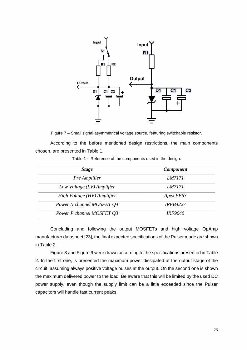
paragraphs, the small signal voltage supply and the VBE multiplier [22].
The voltage supply implemented for the small signal stage is not symmetrical. This
is mandatory in order to be able to achieve the necessary positive voltage at the output of
the small signal OpAmp without exceed the absolute maximum ratings of the device, in
terms of maximum supply voltage. Since the maximum required negative output is much
lower than the positive one, a much lower negative supply voltage can be used, keeping
the total supply voltage bellow the limit. The positive voltage at the output of the small signal
OpAmp must achieve a higher value, so it can drive the high voltage one, which has a
limited voltage gain, otherwise it can become instable.
This voltage supply is made with two simple Zener Diode voltage sources, as shown
in Figure 7. The positive one features a switchable resistor that allows to use two different
input positive supply voltages, which has a serious advantage in terms of maximum peak
delivered power, as it will be explained later on. A higher resistor is used to polarize the
Zener with the same required current for a higher input supply voltage, otherwise, i.e. with
a fixed resistor, the current across the Zener would vary too much for two different supply
voltages.
The VBE multiplier has been designed to dissipate very low power, thus a less
powerful heatsink will be required in here (comparing with the output stage). This stage will
act as a DC voltage source, keeping the last stage polarized in AB class, introducing the
before mentioned advantages.
The connection between the high voltage amplifier and the next stage is made
through the gate node of the P-type MOSFET, being connected to the N-type gate through
the VBE multiplier, this allows the circuit to put more than the supply voltage at the N-type
MOSFET gate, achieving almost the supply voltage at the output of the circuit, during short
pulses. This is possible because during these short pulses the bypass capacitor of the VBE
multiplier voltage source will maintain the voltage at its terminals, allowing higher voltages
to appear at the gate of the N-type MOSFET during short amounts of time. Being possible
to get almost the supply voltage at the output of the high voltage amplifier, at the gate of the
N-type MOSFET the voltage is possible to raise up to this maximum output plus the VBE
multiplier DC value.
23
Figure 7 – Small signal asymmetrical voltage source, featuring switchable resistor.
According to the before mentioned design restrictions, the main components
chosen, are presented in Table 1.
Table 1 – Reference of the components used in the design.
Stage Component
Pre Amplifier LM7171
Low Voltage (LV) Amplifier LM7171
High Voltage (HV) Amplifier Apex PB63
Power N channel MOSFET Q4 IRFB4227
Power P channel MOSFET Q3 IRF9640
Concluding and following the output MOSFETs and high voltage OpAmp
manufacturer datasheet [23], the final expected specifications of the Pulser made are shown
in Table 2.
Figure 8 and Figure 9 were drawn according to the specifications presented in Table
2. In the first one, is presented the maximum power dissipated at the output stage of the
circuit, assuming always positive voltage pulses at the output. On the second one is shown
the maximum delivered power to the load. Be aware that this will be limited by the used DC
power supply, even though the supply limit can be a little exceeded since the Pulser
capacitors will handle fast current peaks.

24
Table 2 – Circuit performance specifications (expected).
Parameter Value
Voltage Gain 80 V/V
Maximum Output Current 200 A
Maximum Average Dissipated Power 30 W
Maximum Peak Dissipated Power 10.000 W (Width < 10 us)
Maximum Delivered Power 25.000 W (Depending on supply voltage)
The total voltage gain was set to 80 V/V so, very low voltage pulse generators are
possible to use without losing any performance (i.e. stability and rise/fall times). The
performance is kept because most of this voltage gain is get from the pre-amplifier stage,
keeping the gain of the high power feedback loop low, thus making it stable.
Figure 8 – Dissipated power on the Pulser, for 130 V supply voltage. Drain Current and Drain-to-Source Voltage at the output Mosfet of the Pulser.
Figure 9 – Delivered power of the Pulser, for 130 V supply voltage.
0 50 100 1500
20
40
60
80
100
120
140
160
180
200
220
Drain to Source Voltage (V)
Dra
in C
urr
ent
(A)
Maximum Dissipated Power
Maximum Dissipated Power
Peak Dissipated Power (width < 10us)
0 50 100 1500
20
40
60
80
100
120
140
160
180
200
220
Output Voltage (V)
Load C
urr
ent
(A)
Maximum Delivered Power
Maximum Delivered Power
Peak Delivered Power (width < 10us)

25
Input
Output
Analysing these last figures, it is possible to see that the delivered power capability
of the circuit is very high. Any weakness in this point of view will only be detected
characterizing very low loads, which can require high current for low output voltages,
condition in which the Pulser is dissipating most of the power. This effect can be reduced
by switching the supply voltage, as said before. Taking advantage of the two different
resistors used in the low voltage supply, the output voltage can be set between 60 V and
130 V, depending on the needs for each DUT, without affecting the performance of the
circuit. By changing the supply voltage to a smaller value less power is dissipated in the
circuit for the same output current and voltage. This is suitable when the output voltage
needs are low. A future option will be, for example, the possibility to characterize the triode
region of a MOSFET using a 60 V supply voltage, and the saturation region using a 130 V
one, to be able of achieving higher 𝑉𝐷𝑆 values.
2.2. Design and Implementation of the Board
After completing the design, the layout of the circuit, including all the components,
was drawn and one Printed Circuit Board (PCB) made. During this step the maximum
current at each line and maximum voltage between them was took into account to calculate
the appropriated line width and spacing. That is why, as it can be analysed in Figure 10,
the output and supply voltage rail lines (bottom) are wider, and considerably more distant
from the other ones. In the low voltage stage (top left) a ground plane has been added to
protect the signals from interferences and noise.
Figure 10 – Top layer drawing of the Pulser PCB.

26
Once all the components have been assembled in the board and the proper heatsink
fixed, the board was tested block-by-block in order to verify that it was assembled correctly.
This block-by-block test makes easier to find the origin of more complex problems that can
be detected in future tests, because it guarantees that each block is doing what is expected.
A photograph of the complete Pulser is shown in Figure 11, were the following
stages can be observed:
On the right half: The power inputs; The low voltage supplies created for the small
signal stage; The small signal stage itself, enclosed by a ground shielding to protect
the low voltage signals processed there from external noise and internal
interferences caused by higher voltage stages;
On the left half: The high voltage OpAmp and the high power MOSFETs, screwed
to the heatsink; The VBE multiplier voltage source, in the bottom left corner.
Figure 11 – Photograph of the Pulser after fully assembled.
2.3. Validation and Test
Some block-by-block tests were done before, right after the implementation of the
Pulser, now it is time to do some complete robustness tests, with the same signals that the
circuit will handle during its normal operation.
First, the simulated and real response of the Pulser will be compared. One simple
approach was used for this test, the loads shown in Figure 12, among some others, have
been characterized, using a VNA to obtain some measurements. Those measurements
were imported to Advance Design System (ADS), and then converted into a netlist of
Output
Input

27
lumped components, using the Broad Band Spice Model (BBSM) generator, function
available in this software. After, before these created models can be used, they need to be
validated. The way it was done, was comparing the response of these loads using harmonic
balance (HB) simulation, which use directly the measured S-parameters files, with the
response to the same input stimulus using transient analysis, which use the BBSM
generated before.
Figure 12 – Loads used to characterize the Pulser (4 Ω on the left and 50 Ω on the right).
As confirmed by the comparison made and shown in Figure 13 and Figure 14, the
model is accurate enough to be assumed that the load generated is the representation of
the real load, which will be used to test the Pulser in the laboratory.
Figure 13 – Comparison between HB simulations and transient ones.
Figure 14 – Calculated approximation error (difference between simulations), presented in dB.

28
Then, each of the loads has been connected to the circuit output, in the lab and in
the simulator. After, a pulse signal was applied to each case and the current/voltage into/at
each load under this normal pulsed operation, for each pulse amplitude, has been
measured at the lab and in the simulator. Finally, the measured result (blue) was compared
with the simulated one (black) in Figure 15 and Figure 16, with the aim of verifying the
simulation accuracy, and validate if it represents with accuracy the implemented circuit.
Figure 15 – Comparison between simulations (Black) and measurements (Blue), for the 50 Ω load.
Figure 16 – Comparison between simulations (Black) and measurements (Blue), for the 4 Ω load.
Since the results of the last simulations were close enough, despite of some DC
value error, it can be assumed that no major error was done during the assembly. Now,
new simulations can be done to predict the behaviour of the circuit with different loads,
before their characterization in the laboratory. This is very useful to know what to expect
before pulsing the real load, and then adjust some settings of the Pulser, if necessary, until
its response becomes the closest possible to the simulated one. In Figure 17 are the
simulated results for a large capacitive load and one equation defined load that has a similar
behaviour to that of a transistor.
0 5 10 15 20 25 30-10
0
10
20
30
40
50
60
Tempo (us)
VD
S (
V)
Measured versus Simulated Voltage [50V] [50Ohm]
0 5 10 15 20 25 30-0.2
0
0.2
0.4
0.6
0.8
1
1.2
Tempo (us)
IDS
(A
)
Measured versus Simulated Current [50V] [50Ohm]
0 5 10 15 20 25 30-10
0
10
20
30
40
50
60
Tempo (us)
VD
S (
V)
Measured versus Simulated Voltage [50V] [4Ohm]
0 5 10 15 20 25 30-2
0
2
4
6
8
10
12
14
Tempo (us)
IDS
(A
)
Measured versus Simulated Current [50V] [4Ohm]

29
Figure 17 – Simulated response of the Pulser with one capacitive load of 10 nF, on the left, and one equation defined load that simulates the behavior of one Transistor, on the right.
After this first set of tests and before start using this equipment to perform real
characterization of RF Power Devices a second complete and powerful set of tests was
performed. First a very low resistive load will be pulsed in order to analyze the power
capability of this system, then some high power and high voltage devices will be used to
test again the response of this hardware but this time with real RF devices.
The used load to test the maximum power capabilities of the Pulser is composed by
four resistors of 10 Ω each, connected in parallel to obtain an approximately 2.5 Ω resistor.
The rated power of this test resistor is approximately 4 W, which is not important in this test,
since all the signals will be very short, presenting a very low duty cycle as well. In the Figure
18 a photograph of the assembled load is shown.
Figure 18 – 2.5 Ω test load, used for high peak power tests.
The result of this test is shown in Figure 19, as it can be analyzed the maximum
tested power was around 5000 W, which is not the maximum possible but more than enough
for the characterization of the devices used nowadays in the industry.
Finally some RF devices were tested, starting from the lower power ones up to a 220
W device. The measurements on this last high power device were performed very
successfully and are presented in Figure 19. In this one it is possible to observe that
measurements up to 120 V, more than 25 A and around 600 W are possible in a RF device.
The output power has been limited to approximately 600 W in the last test in order to protect
the RF device.

30
Figure 19 – Results of the high power test performed in the previous 2.5 Ω shown load.
Figure 20 - Results of the characterization of a 220 W “rated” RF device, limited to a maximum Pulsed DC power of approximately 600 W.
After all the tests done the Pulser is verified to work as expected with any RF device,
the maximum output voltage is the same as expected (around 120 V), the maximum tested
current was 46 A, which is more than enough for the practical use of the circuit. The
maximum tested output power was around 5000 W which is much lower than the initially
expected 25000 W and probably almost the maximum output power. This difference in the
power is caused by the higher series parasitic resistance at the output of the circuit, which
cause a voltage drop for very high output currents. This series resistance is caused by
unconsidered elements in the first predictions, such as the connector, the microstrip lines,
stabilization resistors (added posteriorly) and obviously the used connection cables.
Finally, the time response of the circuit was tested, being the average settling time
even lower than the initially expected 400 ns, as seen in Figure 21 (300 ns). However, as it
will be analyzed in the next chapter, the Pulser is not the component that will set the rise or
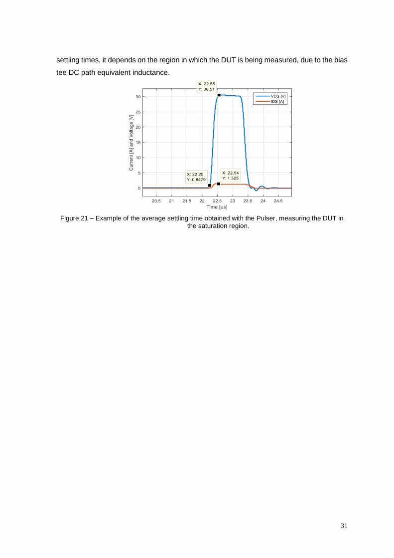
31
settling times, it depends on the region in which the DUT is being measured, due to the bias
tee DC path equivalent inductance.
Figure 21 – Example of the average settling time obtained with the Pulser, measuring the DUT in the saturation region.

32

33
3. DC-IV Characterization of a Radio Frequency Transistor
In the first section of this chapter, some of the issues and phenomena in the scope of
this characterization work, that have been set out in the introduction, will be better discussed
and analysed. The technics and signals used to pulse the device will be explained in this
contest, as well.
Then, the previous obtained results will be analysed and discussed in order to identify
some of the non-linear phenomena present in this transistors technology.
3.1. Inherent Problems and Used Technics During the Characterization
The first problem, and the most inherent one, is about average dissipated power.
One device cannot dissipate more than a certain, and rated power, but it can operate for
short amounts of time in that conditions, that is because the device does not warm up
instantaneously, due to his mass. While for DC operation the warming of the device can be
modulated and explained as a thermal resistor, since it has a linear behaviour, with Kelvin
(K) per Watt (W) units, for pulsed operation the model should include a thermal capacitance
with Joule (J) per (K) units, as well.
The resistance can be seen as the ease of dissipate power or, in other words, the
opposition of the material to the heat flow. The capacitance, as the needed amount of heat
(J, or W∙s) to raise the temperature of the device, normally it is higher as higher is the mass
of the device. In this electrical equivalent analysis, presented in Figure 22 [24], the power
is analysed as a current and the temperature is the voltage at each node. The fact that there
is a capacitance allow high power pulses for the reason that when the power goes, as a
current, through the thermal resistance, the temperature raises, as a voltage. This raise
makes some power (current) pass through the thermal capacitance, letting it store some
energy (heat), therefore less power (current) pass through the resistor allowing the
temperature (voltage) to stay lower.
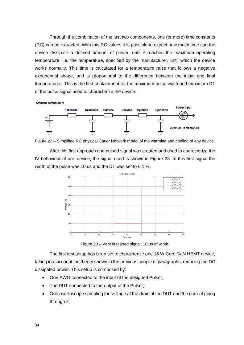
34
Through the combination of the last two components, one (or more) time constants
(RC) can be extracted. With this RC values it is possible to expect how much time can the
device dissipate a defined amount of power, until it reaches the maximum operating
temperature, i.e. the temperature, specified by the manufacturer, until which the device
works normally. This time is calculated for a temperature raise that follows a negative
exponential shape, and is proportional to the difference between the initial and final
temperatures. This is the first containment for the maximum pulse width and maximum DT
of the pulse signal used to characterize the device.
Figure 22 – Simplified RC physical Cauer Network model of the warming and cooling of any device.
After this first approach one pulsed signal was created and used to characterize the
IV behaviour of one device, the signal used is shown in Figure 23. In this first signal the
width of the pulse was 10 us and the DT was set to 0.1 %.
Figure 23 – Very first used signal, 10 us of width.
The first test setup has been set to characterize one 15 W Cree GaN HEMT device,
taking into account the theory shown in the previous couple of paragraphs, reducing the DC
dissipated power. This setup is composed by:
One AWG connected to the input of the designed Pulser;
The DUT connected to the output of the Pulser;
One oscilloscope sampling the voltage at the drain of the DUT and the current going
through it;
0 5 10 15 20 25 30 35 400
10
20
30
40
50
60
First VDS Pulses
Time (us)
Voltage (
V)
VDS = 1
VDS = 10
VDS = 30
VDS = 60

35
Several voltage sources to supply the needed power to the Pulser and bias the
DUT’s gate.
The idea is to Pulse the Drain with different values of 𝑉𝐷𝑆, each of them to different
𝑉𝐺𝑆 values as well, sample the current and the actual applied 𝑉𝐷𝑆, then plot the IV
characteristic of the DUT. The test setup schematic is in Figure 24.
Figure 24 – First test setup used to characterize the device.
After putting all the required equipment’s together and load the first set of pulses,
the rise time obtained was verified to be much higher than the one obtained with resistive
loads. The cause was found to be the Bias Tee, which is required to present stable
impedances to the transistor at high frequencies, and later, allow the measurement of S-
parameters. Since the Bias Tee DC path filter is made of an inductive element, the
equivalent impedance presented by this element will be as higher as higher is the frequency
of the signals passing through it. As the used signal has components up to 10MHz and in
the triode region the DUT presents very low impedances, all the voltage will drop across the
bias tee. This causes the required 𝑉𝐷𝑆, at the drain of the DUT, to raise very slowly. This
happens because, since the 𝑉𝐷𝑆 values in the triode region are very low, the maximum
voltage drop across the DC path of the bias tee will be small. This, keeping in mind that the
derivative of the current is proportional to the voltage drop in an inductive element, causes
the current to raise very slowly.
In order to keep the rise time low, a modification has been done to the pulse shape,
the solution was to perform some signal shaping to the lowest voltage pulses, the ones
which polarize the DUT in the triode region. One very fast and much higher peak was added
right before the desired amplitude pulse, as shown in Figure 25.
This first peak in the output voltage will put a higher voltage drop across the
inductance, thus will make the current rise faster, achieving the desired output quicker. For
the higher voltage pulses, which polarize the device in the saturation region, this is not

36
needed since the output voltage is already enough to rapidly raise the current in the
inductance.
The first DC-IV characteristic, obtained from the sampled pulses shown in Figure
26, is now presented in Figure 27, it is affected by many phenomena, which are explained
through this chapter.
Figure 25 – Example of the required signal shaping.
Figure 26 – Example of one 𝑣𝐷𝑆 and 𝑖𝐷𝑆 pulse, measured during the characterization the DUT.
Figure 27 – First DC-IV characteristic curves, measured for the 15 W Cree GaN.
0 5 10 15 20 25 30 35 40-20
0
20
40
60
Tempo (us)
VD
S (
V)
0 5 10 15 20 25 30 35 40-1
0
1
2
3
4
Tempo (us)
IDS
(A
)
0 5 10 15 20 25 30 35 40 45 500
0.5
1
1.5
2
2.5
3
3.5
4Pulsed DC-IV Curves (Trapping and Temperature)
VGS (V)
IDS
(A
)
VGS = -3.5V
VGS = -3V
VGS = -2.5V
VGS = -2V
VGS = -1.5
VGS = -1
VGS = -0.5V
VGS = 0V
VGS = 0.5V
VGS = 1V
VGS = 1.5V
37
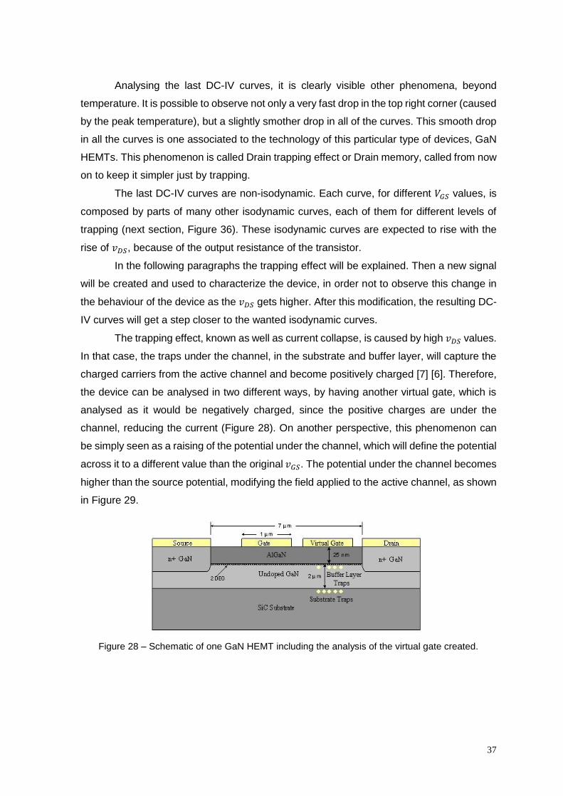
Analysing the last DC-IV curves, it is clearly visible other phenomena, beyond
temperature. It is possible to observe not only a very fast drop in the top right corner (caused
by the peak temperature), but a slightly smother drop in all of the curves. This smooth drop
in all the curves is one associated to the technology of this particular type of devices, GaN
HEMTs. This phenomenon is called Drain trapping effect or Drain memory, called from now
on to keep it simpler just by trapping.
The last DC-IV curves are non-isodynamic. Each curve, for different 𝑉𝐺𝑆 values, is
composed by parts of many other isodynamic curves, each of them for different levels of
trapping (next section, Figure 36). These isodynamic curves are expected to rise with the
rise of 𝑣𝐷𝑆, because of the output resistance of the transistor.
In the following paragraphs the trapping effect will be explained. Then a new signal
will be created and used to characterize the device, in order not to observe this change in
the behaviour of the device as the 𝑣𝐷𝑆 gets higher. After this modification, the resulting DC-
IV curves will get a step closer to the wanted isodynamic curves.
The trapping effect, known as well as current collapse, is caused by high 𝑣𝐷𝑆 values.
In that case, the traps under the channel, in the substrate and buffer layer, will capture the
charged carriers from the active channel and become positively charged [7] [6]. Therefore,
the device can be analysed in two different ways, by having another virtual gate, which is
analysed as it would be negatively charged, since the positive charges are under the
channel, reducing the current (Figure 28). On another perspective, this phenomenon can
be simply seen as a raising of the potential under the channel, which will define the potential
across it to a different value than the original 𝑣𝐺𝑆. The potential under the channel becomes
higher than the source potential, modifying the field applied to the active channel, as shown
in Figure 29.
Figure 28 – Schematic of one GaN HEMT including the analysis of the virtual gate created.

38
Figure 29 – Schematic of one GaN HEMT where the positive charges are shown, trapped in the Buffer and Substrate layers.
As it was explained before, trapping becomes charged with high applied 𝑣𝐷𝑆 values,
reducing the transcondutance of the device, thus, changing the device itself. Since the
discharging time of this phenomenon is much higher than the charging time, as
demonstrated in Figure 30, different behaviours will be observed depending on the last 𝑣𝐷𝑆
bias state, which means that non isodynamic behaviour will be observed. To exclude this
effect from the measurements, it is needed to have the phenomenon in one known stable
state. This is only possible in the charged state, for the reason that it charges very fast and
would not be possible to measure high 𝑣𝐷𝑆 states fast enough, i.e. before the traps becomes
charged.
Figure 30 – Comparison between the traps charging (some nanoseconds, top) and discharging (hundreds of milliseconds, bottom) times.
5 10 15 20 25
0
10
20
30
40
Tempo (us)
VD
S (
V)
5 10 15 20 25
0
0.5
1
X: 5.108Y: 0.2659
Tempo (us)
IDS
(A
)
X: 19.85Y: 0.268
500 550 600 650 700 750 800
0
5
10
15
Tempo (ms)
VD
S (
V)
500 550 600 650 700 750
0.2
0.3
0.4
0.5
0.6 X: 499.8Y: 0.5013
Tempo (ms)
IDS
(A
)
X: 700.2Y: 0.504
39
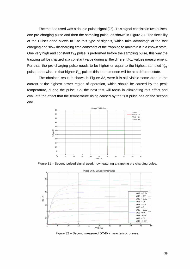
The method used was a double pulse signal [25]. This signal consists in two pulses,
one pre charging pulse and then the sampling pulse, as shown in Figure 31. The flexibility
of the Pulser done allows to use this type of signals, which take advantage of the fast
charging and slow discharging time constants of the trapping to maintain it in a known state.
One very high and constant 𝑉𝐷𝑆 pulse is performed before the sampling pulse, this way the
trapping will be charged at a constant value during all the different 𝑉𝐷𝑆 values measurement.
For that, the pre charging pulse needs to be higher or equal to the highest sampled 𝑉𝐷𝑆
pulse, otherwise, in that higher 𝑉𝐷𝑆 pulses this phenomenon will be at a different state.
The obtained result is shown in Figure 32, were it is still visible some drop in the
current at the highest power region of operation, which should be caused by the peak
temperature, during the pulse. So, the next test will focus in eliminating this effect and
evaluate the effect that the temperature rising caused by the first pulse has on the second
one.
Figure 31 – Second pulsed signal used, now featuring a trapping pre charging pulse.
Figure 32 – Second measured DC-IV characteristic curves.
0 5 10 15 20 25 30 35 40 45 500
5
10
15
20
25
30
35
40
45
50
55
Time (us)
Voltage (
V)
Second VDS Pulses
VDS = 1
VDS = 10
VDS = 30
VDS = 50
0 5 10 15 20 25 30 35 40 45 500
0.5
1
1.5
2
2.5
3
3.5
4Pulsed DC-IV Curves (Temperature)
VGS (V)
IDS
(A
)
VGS = -3.5V
VGS = -3V
VGS = -2.5V
VGS = -2V
VGS = -1.5
VGS = -1
VGS = -0.5V
VGS = 0V
VGS = 0.5V
VGS = 1V
VGS = 1.5V
40
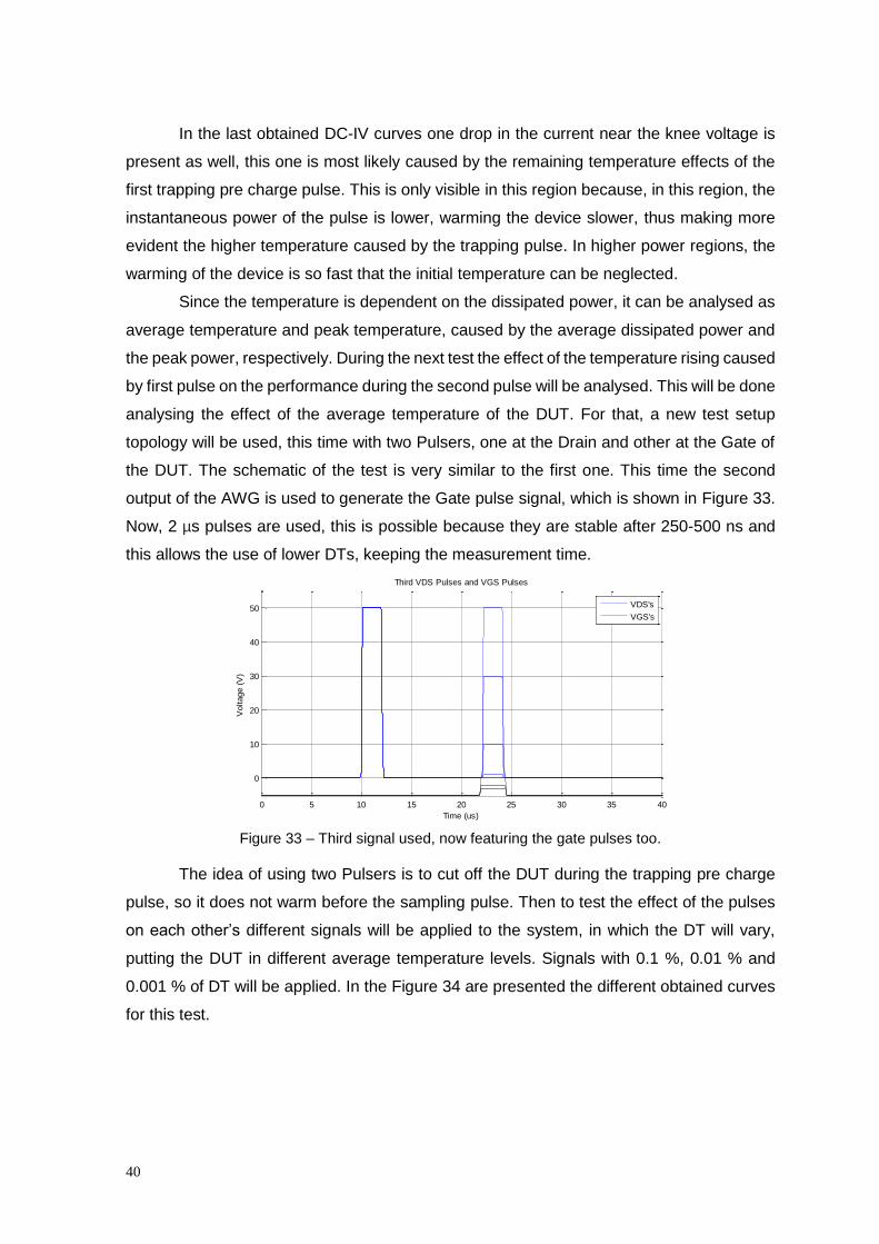
In the last obtained DC-IV curves one drop in the current near the knee voltage is
present as well, this one is most likely caused by the remaining temperature effects of the
first trapping pre charge pulse. This is only visible in this region because, in this region, the
instantaneous power of the pulse is lower, warming the device slower, thus making more
evident the higher temperature caused by the trapping pulse. In higher power regions, the
warming of the device is so fast that the initial temperature can be neglected.
Since the temperature is dependent on the dissipated power, it can be analysed as
average temperature and peak temperature, caused by the average dissipated power and
the peak power, respectively. During the next test the effect of the temperature rising caused
by first pulse on the performance during the second pulse will be analysed. This will be done
analysing the effect of the average temperature of the DUT. For that, a new test setup
topology will be used, this time with two Pulsers, one at the Drain and other at the Gate of
the DUT. The schematic of the test is very similar to the first one. This time the second
output of the AWG is used to generate the Gate pulse signal, which is shown in Figure 33.
Now, 2 µs pulses are used, this is possible because they are stable after 250-500 ns and
this allows the use of lower DTs, keeping the measurement time.
Figure 33 – Third signal used, now featuring the gate pulses too.
The idea of using two Pulsers is to cut off the DUT during the trapping pre charge
pulse, so it does not warm before the sampling pulse. Then to test the effect of the pulses
on each other’s different signals will be applied to the system, in which the DT will vary,
putting the DUT in different average temperature levels. Signals with 0.1 %, 0.01 % and
0.001 % of DT will be applied. In the Figure 34 are presented the different obtained curves
for this test.
0 5 10 15 20 25 30 35 40
0
10
20
30
40
50
Time (us)
Voltage (
V)
Third VDS Pulses and VGS Pulses
VDS's
VGS's

41
Figure 34 – DC-IV characteristic curves obtained for different tested DTs.
Taking a closer look at the last image it is possible to identify a drop in the current
between the measurements, which vary only in the DT. This means that the DUT takes
some milliseconds, time between pulses, Off Time (𝑇𝑜𝑓𝑓), to cool down from the last pulse.
The important conclusions to attain from this experiment are:
The transistor needs to be cut off during the first pulse;
A DT of 0.1 % can’t be used to characterize this device;
0.001 % or at least 0.01 % DT should be used for DC-IV characterization.
Using lower DTs the measurements will require more time to be performed. Another
important conclusion is that the observed drop in the current near the knee voltage,
observed in the last DC-IV curves (Figure 32) was, in fact, caused by the warming produced
by the trapping pre charge pulse, as expected. This can be concluded comparing these
curves with the ones shown in Figure 34, in which during the trapping pre charge pulse the
DUT is in the cut off state.
Notice that, in Figure 34, the drop in the current is more perceptible at lower power
regions. For those in which the power is very high, as explained before, the temperature
change right after the beginning of the pulse is so fast that we can’t even notice the
difference due to the average temperature.
Finally, some tests were done with the last test setup and the determined optimal
signal, the third one, with 0.001 % DT. The complete result set is shown at the next sub
chapter, for now, one set of DC-IV curves is analysed, in Figure 35. This analysis makes
clear that some temperature effects are still present in the highest power region, which can
be attenuated by sampling the DC-IV values closer to the beginning of the pulse.
0 5 10 15 20 25 30 35 40 45 500
0.5
1
1.5
2
2.5
3
3.5
4IV Curves (Duty Cycle Comparison)
VDS (V)
IDS
(A
)
VGS = -3
VGS = -2
VGS = -1
VGS = 0
VGS = 1
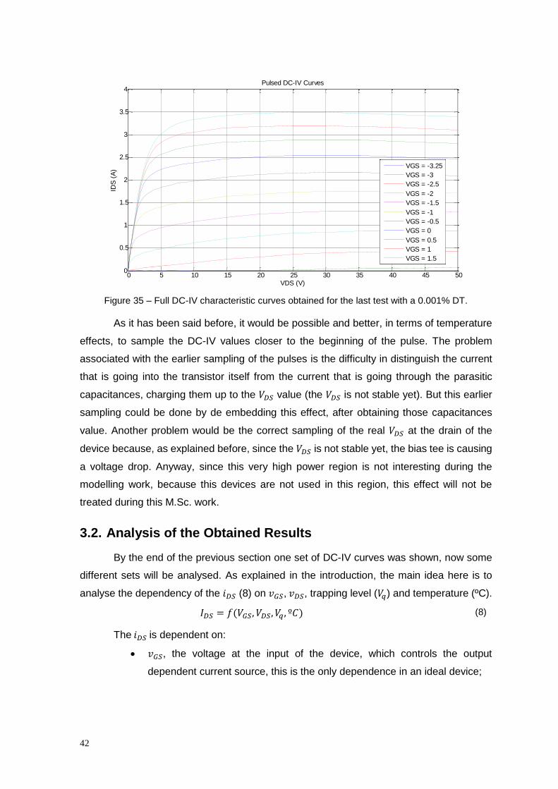
42
Figure 35 – Full DC-IV characteristic curves obtained for the last test with a 0.001% DT.
As it has been said before, it would be possible and better, in terms of temperature
effects, to sample the DC-IV values closer to the beginning of the pulse. The problem
associated with the earlier sampling of the pulses is the difficulty in distinguish the current
that is going into the transistor itself from the current that is going through the parasitic
capacitances, charging them up to the 𝑉𝐷𝑆 value (the 𝑉𝐷𝑆 is not stable yet). But this earlier
sampling could be done by de embedding this effect, after obtaining those capacitances
value. Another problem would be the correct sampling of the real 𝑉𝐷𝑆 at the drain of the
device because, as explained before, since the 𝑉𝐷𝑆 is not stable yet, the bias tee is causing
a voltage drop. Anyway, since this very high power region is not interesting during the
modelling work, because this devices are not used in this region, this effect will not be
treated during this M.Sc. work.
3.2. Analysis of the Obtained Results
By the end of the previous section one set of DC-IV curves was shown, now some
different sets will be analysed. As explained in the introduction, the main idea here is to
analyse the dependency of the 𝑖𝐷𝑆 (8) on 𝑣𝐺𝑆, 𝑣𝐷𝑆, trapping level (𝑉𝑞) and temperature (ºC).
𝐼𝐷𝑆 = 𝑓(𝑉𝐺𝑆, 𝑉𝐷𝑆, 𝑉𝑞 , º𝐶) (8)
The 𝑖𝐷𝑆 is dependent on:
𝑣𝐺𝑆, the voltage at the input of the device, which controls the output
dependent current source, this is the only dependence in an ideal device;
0 5 10 15 20 25 30 35 40 45 500
0.5
1
1.5
2
2.5
3
3.5
4Pulsed DC-IV Curves
VDS (V)
IDS
(A
)
VGS = -3.25
VGS = -3
VGS = -2.5
VGS = -2
VGS = -1.5
VGS = -1
VGS = -0.5
VGS = 0
VGS = 0.5
VGS = 1
VGS = 1.5

43
𝑣𝐷𝑆, since the device is not perfect, the output current will depend on the
output voltage as well, i.e. for low 𝑣𝐷𝑆 values the current is lower than in one
ideal device, this is called the triode region. There is, as well, a small raise
in the current for high 𝑣𝐷𝑆 values, due to the output conductance of the
device;
Temperature, the output current is dependent on the temperature, it will
become lower when the device gets warmer and is operating in the strong
inversion zone. Or become higher when it is in the weak inversion mode.
During this analysis, the temperature will be considered constant and as
close as possible to the ambient temperature;
Trapping charge level, which makes 𝑖𝐷𝑆 as lower as higher is the 𝑣𝐷𝑆, it will
be considered constant and charged with a pre pulse, which known voltage
level will be called 𝑉𝑞. This variable will be swept, since the idea is to analyse
how the behaviour of the device changes with the change of this
phenomenon state.
In Figure 36, DC-IV curves for different 𝑉𝑞 voltages and four different 𝑣𝐺𝑆 are shown,
in the 𝑖𝐷𝑆/𝑣𝐷𝑆 plane. As it can be observed, the current becomes lower with the charging of
the traps and as lower as higher is the charging level. It is possible to get an isodynamic
behaviour for different levels of charging, up to the 𝑣𝐷𝑆 level of the pre pulse (𝑉𝑞) used,
above this value the traps will be charged (very fast) to the level of the measured 𝑣𝐷𝑆 and
the behaviour of the transistor for that 𝑣𝐺𝑆 becomes a different one.
Figure 36 – DC-IV curves in the 𝑖𝐷𝑆/𝑣𝐷𝑆 plane for different 𝑣𝐺𝑆 and 𝑉𝑞 values.
0 5 10 15 20 25 30 35 40 45 500
0.5
1
1.5
2
2.5
3
3.5
4Pulsed DC-IV Curves (Different Vpre)
VDS (V)
IDS
(A
)
VGS = -3
VGS = -2
VGS = -1
VGS = 0
VGS = 1

44
In this 𝑖𝐷𝑆/𝑣𝐷𝑆 plane some parameters are easy to analyse, such as the Knee
voltage, maximum current and device’s output conductance.
From the last results and previous analysis some values for this device parameters
can be obtained, as function of the 𝑣𝐺𝑆, 𝑣𝐷𝑆 and trapping. Table 3 shows the maximum
current for a 𝑣𝐺𝑆 of 1 V and different trapping states. An 8% drop is observed for the higher
trapping charge level. This will affect many important parameters, such as the maximum
delivered power, as explained in the first chapter of this work.
Table 3 – Drain current for a 𝑣𝐺𝑆 of 1 V and 𝑣𝐷𝑆 of 15 V, as function of the trapping level.
Pre Trapping Voltage Drain Current (@15V)
15 V 3.42 A
23.75 V 3.35 A
32.5 V 3.29 A
41.25 V 3.21 A
50 V 3.15 A
Following, the dependency of the 𝑖𝐷𝑆 on the 𝑉𝑞 is again analysed, but this time in the
𝑖𝐷𝑆/𝑣𝐺𝑆 plane where it is easier to analyse other parameters, as the Threshold Voltage (𝑉𝑇),
and the transcondutance.
In Figure 37 the trapping level is fixed at 50 V and the 𝑖𝐷𝑆 dependency on the 𝑣𝐺𝑆 is
analysed for different 𝑣𝐷𝑆 values.
Figure 37 – DC-IV curves in the 𝑖𝐷𝑆/𝑣𝐺𝑆 plane for a 50 V fixed pre trapping pulse and different
values of 𝑣𝐷𝑆.
-3.5 -3 -2.5 -2 -1.5 -1 -0.5 0 0.5 1 1.5 20
0.5
1
1.5
2
2.5
3
3.5
4Pulsed DC-IV Curves
VGS (V)
IDS
(A
)
VDS = 0.25
VDS = 1
VDS = 3
VDS = 4
VDS = 5
VDS = 9
VDS = 25
VDS = 50

45
Note that the triode region is very evident in this plane as well. The current for a
fixed 1 V 𝑣𝐺𝑆 is higher when the 𝑣𝐷𝑆 is higher, up to a certain value which is called in the
𝑖𝐷𝑆/𝑣𝐺𝑆 plane by knee voltage. Then the device is almost linear, the current is almost the
same for every 𝑣𝐷𝑆 value. In this last case the current depends mostly on the input, 𝑣𝐺𝑆, it
can be said that the device is working in the saturation region.
In Figure 38, a different analysis of the obtained results is presented, the 𝑣𝐷𝑆 is set
constant at 8 V and the resultant 𝑖𝐷𝑆 depends on the trapping level. Two different values of
𝑣𝐷𝑆 are used in the trapping pre pulse, 15 and 50 V, keeping the main 𝑣𝐷𝑆 pulse constant
at 8 V. Here a change on the 𝑉𝑇 is clearly visible. The 𝑉𝑇 is higher when the trapping is
charged to a higher voltage.
Figure 38 – DC-IV curves in the 𝑖𝐷𝑆/𝑣𝐺𝑆 plane for 8 V 𝑣𝐷𝑆 and different 𝑉𝑞 ’s.
From the last figure and some identical curves for other trapping charge values, the
Table 4 was obtained in which the 𝑉𝑇 is revealed as function of the trapping voltage level,
for an 8 V 𝑉𝐷𝑆 value.
Table 4 – Variation of the 𝑉𝑇, for different trapping states, and fixed 𝑣𝐷𝑆 of 8 V.
Pre Trapping Voltage Threshold Voltage (@20mA)
15 V -3.12 V
23.75 V -3.03 V
32.5 V -2.96 V
41.25 V -2.93 V
50 V -2.90 V
-3.5 -3 -2.5 -2 -1.5 -1 -0.5 0 0.5 1 1.5 20
0.5
1
1.5
2
2.5
3
3.5
4
X: -3.047Y: 0.0004352
Pulsed DC-IV Curves
VGS (V)
IDS
(A
)
X: -3.301Y: 0.0002168
VDS = 8V (Vpre = 15V)
VDS = 8V (Vpre = 50V)

46
Note that an increase of 7 % in the 𝑉𝑇 value is noticed and again it has costs in terms
of performance.
Since there is a maximum allowed input 𝑣𝐺𝑆 value for this technology, if the device
needs to be biased at a higher 𝑣𝐺𝑆 for the same 𝑖𝐷𝑆, the input range will be smaller. Another
consequence is that, for example, in a class B PA the device can become biased in class
C, after reaching full power operation. This will reduce the small signal gain, even if this full
power operation lasts for a short amount of time, because the charging time constants are
very fast.
In Figure 39 [26] it is presented a practical example of an AM/AM characteristic of a
GaN HEMT PA affected by trapping effects. The measurements have been done with a two
tone signal of various peak-envelope-powers (PEP) with a fixed separation frequency (50
kHz) and the PA was biased at 𝐼𝑄 = 2 % 𝐼𝑑𝑠𝑠.
Figure 39 – Measured dynamic gain profiles with two tone of various peak-envelope-power for a GaN HEMT.
It is evident, as explained in the last paragraphs, that the PA is becoming biased in
class C. As the input peak power becomes higher, the trapping is charged and the 𝑉𝑇
changes to higher values. Since 𝑣𝐺𝑆 is kept constant during all the operation, this change
in 𝑉𝑇 causes a change in 𝐼𝑄. If 𝐼𝑄 becomes lower, the PA becomes biased in class C, and
its gain profile changes.
This last analysis makes evident the dynamic behaviour of the device. This dynamic
behaviour makes it more difficult to linearize.

47
4. IV Characterization and Small Signal Analysis Comparison
In this chapter the addition of another utility to the previous setup will be described.
Now it will be possible to measure pulsed S-parameters with the same system, used to
characterize RF devices.
Now it is possible to fully characterize devices using, not only the pulsed DC-IV
measurements, but also pulsed S-parameter measurements. This will make possible the
extraction of extrinsic and intrinsic capacitances and inductances that are not identified
during DC-IV measurements. Taking into account the information about the DC and small
signal behaviour of the device, it is possible to obtain a large signal model which can be
used to design, for example, an amplifier using the same device.
4.1. S-Parameter Measurements
The measurements are performed using a commercial equipment, Agilent N5230C
PNA-X, and the setup is identical to the one described in the previous chapter. This time a
new trigger signal is connected between the used AWG and the VNA in order to perform
accurate wideband S-parameters measurements [27], which need to be sampled during the
DC 𝑉𝐷𝑆 and 𝑉𝐺𝑆 pulses.
In Figure 40 is the complete schematic of the used equipment and respective
connections.
Figure 40 – Complete schematic of the final system.
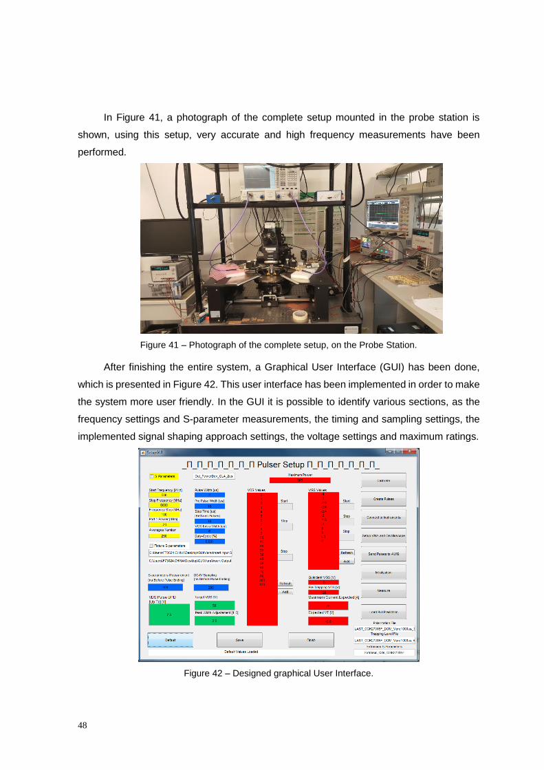
48
In Figure 41, a photograph of the complete setup mounted in the probe station is
shown, using this setup, very accurate and high frequency measurements have been
performed.
Figure 41 – Photograph of the complete setup, on the Probe Station.
After finishing the entire system, a Graphical User Interface (GUI) has been done,
which is presented in Figure 42. This user interface has been implemented in order to make
the system more user friendly. In the GUI it is possible to identify various sections, as the
frequency settings and S-parameter measurements, the timing and sampling settings, the
implemented signal shaping approach settings, the voltage settings and maximum ratings.
Figure 42 – Designed graphical User Interface.

49
The complete setup was used to perform on wafer measurements, using RF Probes,
and SubMiniature Version A (SMA) fixture measurements as well. For the last ones a Thru,
Reflect and Line (TRL) calibration Kit was designed, in order to obtain accurate
measurements up to 10 GHz. This Kit was specially designed to use Nist Multiline TRL
calibration [28], which basically uses all the standard lines and other virtual lines that are
extracted from the length difference between all the physical lines, then for each frequency
the best line is used to characterize the fixture. More information about this TRL calibration
Kit can be found in Appendix A.
A photograph of the designed kit is shown in the Figure 43.
Figure 43 – TRL Calibration Kit used to measure packaged devices.
Using the previous setup the measurements are performed using a pulsed DC signal
with a duty-cycle of 0.1 %. This is not totally enough to obtain isodynamic measurements,
i.e. maintain the temperature, as we proved in the previous chapter. However, this is the
minimum feasible duty-cycle, making the fully characterization of one device last for 3 hours.
Using a duty cycle of 0.01 % which would be the ideal one the measurement of the same
number of bias points and frequencies would take approximately 30 hours, since this cause
many problems, including calibration degradation, the duty cycle was kept at 0.1 %.
The measurements were performed in 200 ns (IFBW of 5 MHz) during a DC pulse
with between 0.8 µs and 1.4 µs of width. In the Figure 44 is shown an example of a pulse
and the intervals where the S-parameters and DC-IV are sampled.
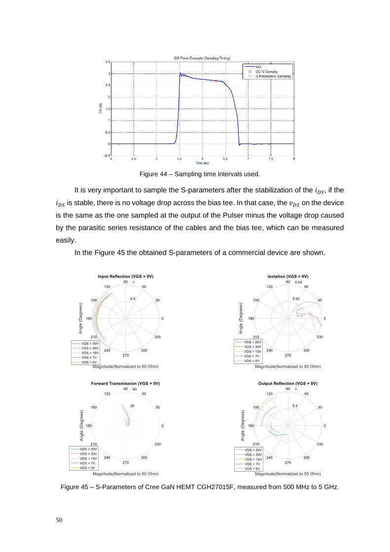
50
Figure 44 – Sampling time intervals used.
It is very important to sample the S-parameters after the stabilization of the 𝑖𝐷𝑆, if the
𝑖𝐷𝑆 is stable, there is no voltage drop across the bias tee. In that case, the 𝑣𝐷𝑆 on the device
is the same as the one sampled at the output of the Pulser minus the voltage drop caused
by the parasitic series resistance of the cables and the bias tee, which can be measured
easily.
In the Figure 45 the obtained S-parameters of a commercial device are shown.
Figure 45 – S-Parameters of Cree GaN HEMT CGH27015F, measured from 500 MHz to 5 GHz.

51
4.2. Transcondutance (gm) and Output Conductance (gds) Deduction and Integration
Using the S-parameters measured and shown during the last chapter the gm and gds
of the device have been extracted, in order to further verify both the accuracy of this
measurements and the Pulsed DC-IV ones.
In Figure 46 is possible to analyse the gm and gds values, measured for the Cree
CGH2715P GaN device. The gm is dependent on the 𝑣𝐺𝑆, being zero when the device is in
the cut off region, achieving high constant values in the middle region and then falling again
due to the conduction limit of the device. It depends on the 𝑣𝐷𝑆 as well, for small 𝑣𝐷𝑆 values
the maximum value is lower and the device conduction saturation happens before, this is
characteristic of the triode region. The gds is high in the triode region (small 𝑣𝐷𝑆 values) and
low in the saturation region. This indicates that the 𝑖𝐷𝑆 is much more dependent on the 𝑣𝐷𝑆
in the triode region than in the saturation region, as it is known.
Figure 46 – Transcondutance (gm) and Output Conductance (gds) of the measured device.
Now, the 𝑖𝐷𝑆 will be analysed as a potential, being the gm and gds the associated
vector fields. It is only possible to obtain a (scalar) potential if the associated vector fields
are conservative [29]. If they are proved to be conservative, the potential obtained from
them, the 𝑖𝐷𝑆, can be considered isodynamic [14]. An isodynamic potential is a function that
can be obtained from the integration of its vector fields, being the result independent of the
followed path [30]. In the case of 𝑖𝐷𝑆 it means that it is independent of the measurement

52
sequence, it doesn’t matter if a 𝑣𝐷𝑆 sweep is made for each 𝑣𝐺𝑆 or vice-versa. This will only
be true if the trapping is not affecting the measurements anymore, other way, the case in
which the gm is integrated in 𝑣𝐺𝑆 for lower values of 𝑣𝐷𝑆 the currents would be higher.
Concluding, the obtained 𝑖𝐷𝑆 can be considered isodynamic if the integration of the gm and
gds following two different paths, produces the same result.
The application of this theorem to prove that the obtained 𝑖𝐷𝑆 is isodynamic is going
to start by the assumption that the vector fields are conservative, going then to verify if that
was a correct assumption or not. Using this analysis it is possible to verify if the fields are
conservative and obtain the wanted potential at the same time, integrating the two different
fields through different paths. If the final result is the same, the obtained result is the wanted
potential, if it is not the same, it means not only that the result is incorrect but that it is not
possible to define potential from this fields as well. In the next few expressions a small
analysis about this theory [31] is shown.
It is known that the 𝑖𝐷𝑆 is obtained from the gradient of, at least, two vector fields, as
shown in the expression (9):
(𝑔𝑚 𝑣𝐺𝑆 + 𝑔𝑑𝑠 𝑣𝐷𝑆 ) = ∇ ∙ 𝑖𝐷𝑆 (9)
It is possible to obtain the 𝑖𝐷𝑆 from these vector fields, as shown by the inversion of
the previous expression:
𝑖𝐷𝑆(𝑣𝐷𝑆0, 𝑣𝐺𝑆) = ∫ 𝑔𝑚 𝑑𝑣
𝑣𝐺𝑆
<𝑣𝑡
+ 0 (10)
𝑖𝐷𝑆(𝑣𝐷𝑆, 𝑣𝐺𝑆0) = ∫ 𝑔𝑑𝑠 𝑑𝑣𝑣𝐷𝑆
0
+ 0 (11)
In order for this last step to be true the two vector fields need to be conservative, the
result of their integration following two different paths must be the same [(10) equal to (11)],
so their rotational need to be equal to zero:
∇ х (𝑔𝑚 𝑣𝐺𝑆 + 𝑔𝑑𝑠 𝑣𝐷𝑆 ) = 0 (12)
Developing a little further the previous expression it is obtained that the two
derivatives of 𝑖𝐷𝑆 shown in the expression (15) must be equal. If the two obtained 𝑖𝐷𝑆 from
the expressions (10) and (11) are equal, the expression (12) and (15) must be true as well,
so the 𝑖𝐷𝑆 has been correctly obtained.
∂𝑔𝑑𝑠
∂𝑣𝑔𝑠−
∂𝑔𝑚
∂𝑣𝑑𝑠= 0
(13)
∂𝑔𝑑𝑠
∂𝑣𝑔𝑠=
∂𝑔𝑚
∂𝑣𝑑𝑠
(14)

53
∂2𝑖𝑑𝑠
∂𝑣𝑑𝑠 ∂𝑣𝑔𝑠=
∂2𝑖𝑑𝑠
∂𝑣𝑔𝑠 ∂𝑣𝑑𝑠
(15)
The gm has been integrated following the expression (10), in order to 𝑣𝐺𝑆 using a
numerical integration algorithm. Since there is no 𝑖𝐺𝑆 the values of the 𝑣𝐺𝑆 sampled at the
output of the Pulser are the same at the device plane, thus this 𝑣𝐺𝑆 values have been directly
used during the integration. In terms of 𝑣𝐷𝑆, it is very important to integrate the gm values
measured for exactly the same 𝑣𝐷𝑆 value, or a variable that is not being used for the
integration will be changed. Since for the same 𝑣𝐷𝑆 value at the output of the Pulser, the
𝑣𝐷𝑆 at the device plane is different, being lower as higher is the 𝑖𝐷𝑆, the gm values have
been sampled for the same 𝑣𝐺𝑆 values but for slightly different 𝑣𝐷𝑆 values. To obtain the
correct integration of these values the gm has been interpolated in order to 𝑣𝐷𝑆 and the
integration has been done using the interpolated gm for exactly the same 𝑣𝐷𝑆 values.
Gds has been integrated, following the expression (11), using the same numerical
algorithm. For this one, since the 𝑣𝐺𝑆 is always constant (does not depend on the 𝑖𝐷𝑆 value)
the integration can be done directly. The only value that varies with the 𝑖𝐷𝑆 is the 𝑣𝐷𝑆 and
since this is the integration variable for the gds, the absolute value of it is not important, as
long as it is known.
In Figure 47 is possible to analyse the 𝑖𝐷𝑆 obtained from the DC-IV measurements,
the 𝑖𝐷𝑆 obtained from the gm integration and the 𝑖𝐷𝑆 obtained from the gds integration. From
the analysis of this curves it can be concluded that the 𝑖𝐷𝑆 obtained from the integration of
the gm is equal to the 𝑖𝐷𝑆 obtained from the integration of the gds. This means that we
obtained a correct value for it and it can be considered isodynamic, i.e. the integration
following different paths has produced the same result.
The DC-IV is the same, so isodynamic too, in almost all the regions except for the
highest power region, as expected, and marked in the figure by the green semi-circle. In
this zone it is very difficult to measure the 𝑖𝐷𝑆 without temperature effects, which are caused
by the immense peak power that is dissipated in the device during the pulse. This peak
power is around 10 times the rated power of the device, approximately 150 W in the case
of this 15 W GaN device.
To achieve an isodynamic behaviour in this region, the measurements would need to
be incredibly fast because this reduction in the 𝑖𝐷𝑆 caused by the instantaneous dissipated
power dissipated is observed in tenths of ns, which is lower than the settling time of the
designed system or any other commercial system. Moreover, as said in the previous
chapter of this work, even if the bias tee and the Pulser would be extremely optimized,
making the measurements much faster, all the parasitic capacitances would need to be
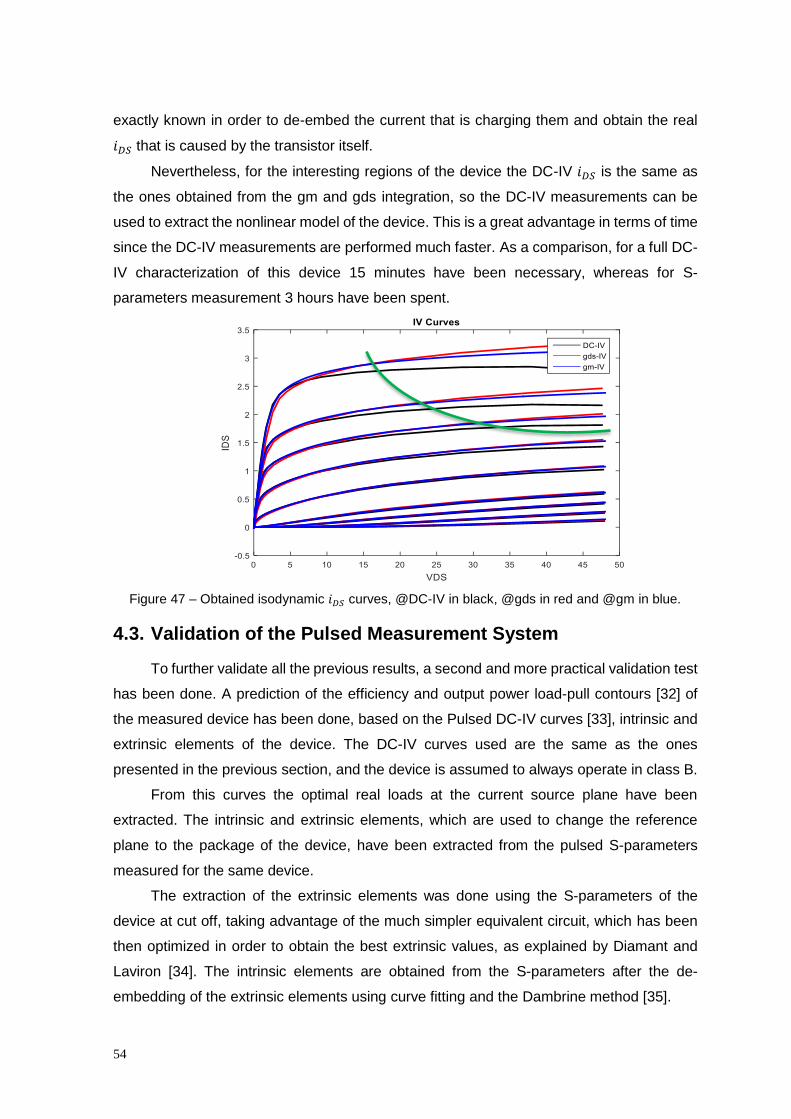
54
exactly known in order to de-embed the current that is charging them and obtain the real
𝑖𝐷𝑆 that is caused by the transistor itself.
Nevertheless, for the interesting regions of the device the DC-IV 𝑖𝐷𝑆 is the same as
the ones obtained from the gm and gds integration, so the DC-IV measurements can be
used to extract the nonlinear model of the device. This is a great advantage in terms of time
since the DC-IV measurements are performed much faster. As a comparison, for a full DC-
IV characterization of this device 15 minutes have been necessary, whereas for S-
parameters measurement 3 hours have been spent.
Figure 47 – Obtained isodynamic 𝑖𝐷𝑆 curves, @DC-IV in black, @gds in red and @gm in blue.
4.3. Validation of the Pulsed Measurement System
To further validate all the previous results, a second and more practical validation test
has been done. A prediction of the efficiency and output power load-pull contours [32] of
the measured device has been done, based on the Pulsed DC-IV curves [33], intrinsic and
extrinsic elements of the device. The DC-IV curves used are the same as the ones
presented in the previous section, and the device is assumed to always operate in class B.
From this curves the optimal real loads at the current source plane have been
extracted. The intrinsic and extrinsic elements, which are used to change the reference
plane to the package of the device, have been extracted from the pulsed S-parameters
measured for the same device.
The extraction of the extrinsic elements was done using the S-parameters of the
device at cut off, taking advantage of the much simpler equivalent circuit, which has been
then optimized in order to obtain the best extrinsic values, as explained by Diamant and
Laviron [34]. The intrinsic elements are obtained from the S-parameters after the de-
embedding of the extrinsic elements using curve fitting and the Dambrine method [35].

55
In Figure 48, the DC-IV curves and the optimal real load lines for maximum delivered
power and drain efficiency are presented, being the load which produces the maximum
efficiency higher than the one which makes the device deliver the maximum power, as
expected. To achieve this performance metrics these real load must be presented at the
current source plane, because the DC-IV measurements do not account for inductive or
capacitive elements.
Figure 48 – 𝑖𝐷𝑆 curve for 𝑣𝐺𝑆 equal to 1 V and respective optimal load lines.
In Figure 49 are shown the load-pull contours at the current source plane, where it is
possible to analyse the dependency of the delivered power or drain efficiency on the load
imaginary part. For imaginary loads, lower power and efficiency are obtained, as expected,
once this results still valid for the current source plane.
After this analysis a different perspective containing the same information can be built
in a graph which correlates the drain efficiency and the output delivered power. This last
one can be observed in Figure 50. In this one is easy to analyse the load-pull Ratio (LPR)
[36] and the efficiency degradation for lower delivered power, which is caused in this simple
analysis, only, by the quiescent current.
Figure 49 – Load-Pull contours, at the current source plane, of the analyzed device. Maximum Efficiency of 73.6 % (5 % step). Maximum Power of 41.6 dBm (1 dBm step).

56
Figure 50 – Drain efficiency vs Output Power characteristic of the device.
The quiescent current (𝐼𝑄) has been set as the current passing through the device
polarized by the 𝑉𝐺𝑆 value at which for an equivalent ideal device it would be polarized at
the threshold voltage (𝑉𝑇). As shown in Figure 51.
Figure 51 – Illustration of the method used to calculate the 𝐼𝑄 and large signal 𝐼𝑄.
This polarization point has been set for a 𝑣𝐷𝑆 equal to the DC 𝑉𝐷𝑆 of the device, in this
case 28 V. Then for the remaining calculations, delivered power and drain efficiency, the 𝐼𝑄
used is the large signal one, i.e., the 𝑖𝐷𝑆 for the previously obtained 𝑣𝐺𝑆 when the device
has a large RF signal applied, which charge the trapping phenomenon to twice the VDD
voltage. This always assuming during the whole project that the amplifier is working as a
class B [37].
Now, in order to design an amplifier using the studied packaged GaN device, it is
necessary, to embed the capacitive and inductive elements in order to obtain the equivalent
load at the package plane. So, the intrinsic elements, such as the Cds, the Miller [22] Cgd
and all of the other extracted extrinsic elements have been embedded.

57
After this embedding, a rotation on the load-pull contours have been observed, which
has been caused mainly by the Cds. The obtained contours are presented in Figure 52, and
have been used to design a class B amplifier for the presented loads. The red circle is the
fundamental frequency load, the green and purple ones are the second and third harmonic
terminations, respectively.
Figure 52 – Load-Pull prediction at the package plane, and design loads used for the PA at the package plane. Maximum Efficiency of 73.6 % (5 % step). Maximum Power of 41.6 dBm
(1 dBm step).
The output matching network (OMN) of the amplifier has been designed using only S-
parameter optimization, to present the design load to the device at the package plane. The
loads presented at the harmonic frequencies are short circuits at the current source plane,
the respective loads at the package plane are two inductive loads.
After designing the output network to present the wanted S-parameters to the device,
its measured S-parameters, at the bias point, were added to the design, as shown in Figure
53. At this point the design was composed by the designed OMN and the measured S-
parameters of the device.
Figure 53 – OMN of the designed PA, and measured S-parameters of the same device, at 28 V of 𝑉𝐷𝑆 polarization.
Adjustment Capacitor
Measured S-parameters
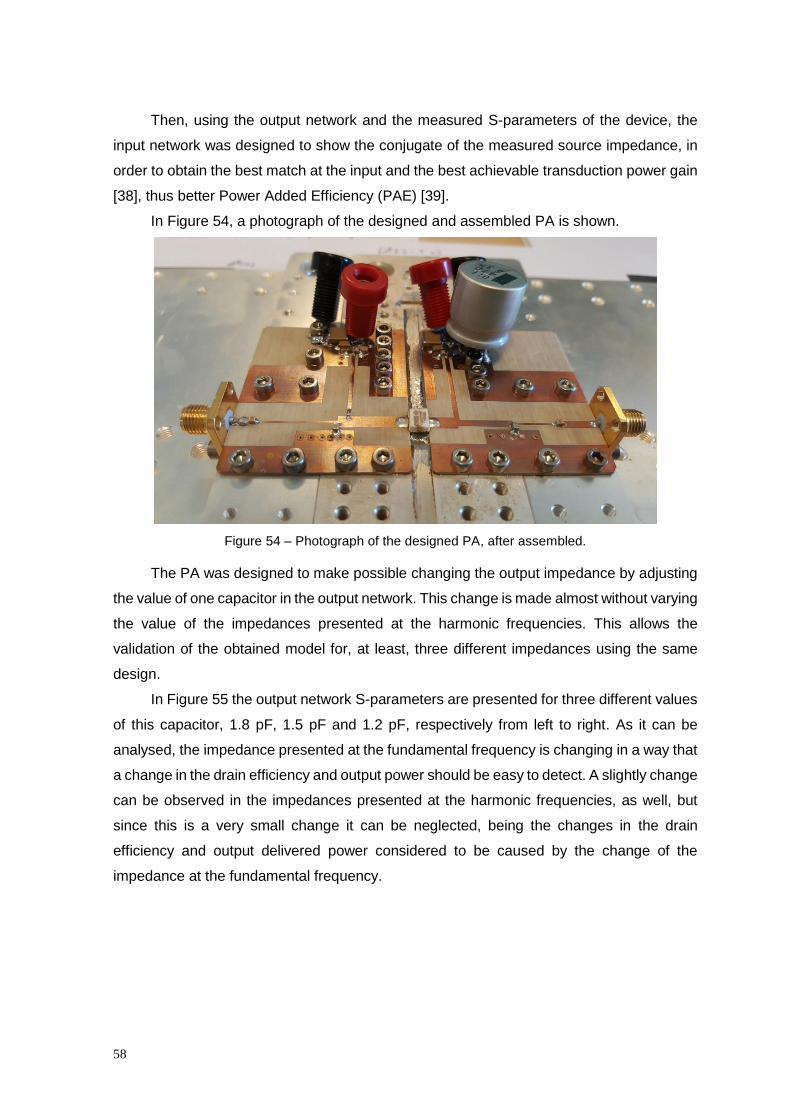
58
Then, using the output network and the measured S-parameters of the device, the
input network was designed to show the conjugate of the measured source impedance, in
order to obtain the best match at the input and the best achievable transduction power gain
[38], thus better Power Added Efficiency (PAE) [39].
In Figure 54, a photograph of the designed and assembled PA is shown.
Figure 54 – Photograph of the designed PA, after assembled.
The PA was designed to make possible changing the output impedance by adjusting
the value of one capacitor in the output network. This change is made almost without varying
the value of the impedances presented at the harmonic frequencies. This allows the
validation of the obtained model for, at least, three different impedances using the same
design.
In Figure 55 the output network S-parameters are presented for three different values
of this capacitor, 1.8 pF, 1.5 pF and 1.2 pF, respectively from left to right. As it can be
analysed, the impedance presented at the fundamental frequency is changing in a way that
a change in the drain efficiency and output power should be easy to detect. A slightly change
can be observed in the impedances presented at the harmonic frequencies, as well, but
since this is a very small change it can be neglected, being the changes in the drain
efficiency and output delivered power considered to be caused by the change of the
impedance at the fundamental frequency.

59
Figure 55 – OMN S-parameters for three different values of the tuning capacitor.
In Figure 56, the measured results of the PA for the three different OMNs are shown.
The power gain and drain efficiency can be analysed at this plots.
Figure 56 – Measured Gain and Drain Efficiency of the designed PA.
Analysing this results a slightly deviation is identified, both in the efficiency and power.
In order to make easier the analysis of the results, they are displayed in Table 5. The results
of drain efficiency and output power have been obtained at approximately 1 dB of power
gain compression.
The chosen level of compression was only 1 dB because this is the value until which
the PA is working in approximately class B and the predicted values are valid, since they
have been deduced from the theoretical class B operation expressions.
Comparing the values presented in the table a maximum deviation of 3.5 % in the
efficiency and 1 dBm in power are observed.
This deviation can be caused by some imperfections during the assembling of the PA.
For example, if a slightly change of the impedances presented at the harmonic frequencies
occur, a little changed in the class of operation occur as well. In this case, some harmonic
conduction can be included in the operation mode of the PA, thus making invalid the used
expressions to calculate the measured metrics.

60
Table 5 – Comparison between the measured and predicted metrics of the designed PA.
Results Comparison Predicted Values Measured Values
Output Power (1.2pF) 40.70 dBm 41.77 dBm
Drain Efficiency (1.2pF) 65.70 % 65.46 %
Output Power (1.5pF) 40.30 dBm 40.43 dBm
Drain Efficiency (1.5pF) 70.70 % 67.28 %
Output Power (1.8pF) 39.10 dBm 39.89 dBm
Drain Efficiency (1.8pF) 71.70 % 69.06 %
Even though, most likely the error observed is caused by the error in the extracted
parasitic elements of the device, which would cause a slightly different rotation in the load-
pull contours, as seen before in this chapter, slightly changing the optimal impedances
obtained for this device.

61
5. Conclusion and Future Work
During this last chapter a complete analysis and evaluation of all the objectives set
up in the beginning of this work and their fulfilment will be done. A description of the work
done and its contribution for the final objective will be written.
Finally, some advices will be given as what could be done to improve the realized
work.
5.1. Conclusion
As a first approach, an intensive study about the existing systems, techniques used
and types of measurements performed has been done. During this stage, the process of
measuring DC-IV characteristics and S-parameters pulsing the device has been
understood. After identifying the best systems available and their performance, a new
measurement system solution has been proposed.
After choosing the system topology and the complete architecture of the
measurement bench, the Pulser head has been designed, simulated and manufactured.
Next, the Pulser has been tested with different signals and loads and finally with real
devices.
The system developed has been used to measure pulsed DC-IV and S-parameters
of devices up to 220 W (rated RF power), practical values of 120 V of maximum 𝑣𝐷𝑆 and 27
A of 𝑖𝐷𝑆 have been used. A maximum tested output power of 5000 W was tested in a
resistive load. In terms of settling time, values between 300 and 800 ns have been obtained,
depending on which region the device being measured is tested (triode or saturation). This
means that pulse widths between 1 and 2 µs can be used to DC-IV characterize a device
in 15 minutes or measure a full set of pulsed S-parameters, using around 200 bias points,
in less than 3 hours.
With this system, whose performance metrics have been described in the previous
paragraph, a full characterization of a RF 15 W Cree device has been successfully done,
which has been verified by two different methods.

62
The first verification done was a complete analysis of the gm and gds obtained from
the pulsed S-parameters measurement, as a conservative field. The result obtained from
this test was affirmative. These parameters were demonstrated to constitute a conservative
vector field, from which has resulted an isodynamic “potential”, the 𝑖𝐷𝑆. Then, to verify the
result of the DC-IV measurements, this gm and gds integrated 𝑖𝐷𝑆 was compared with the
one obtained from direct 𝑖𝐷𝑆 measurement. The DC-IV 𝑖𝐷𝑆 has been considered isodynamic
in every region except for the highest power one, in which no device operates so its
characterization is not interesting. In the interesting region, the DC-IV measurements are
as accurate as the S-parameters ones. This means that they can be very helpful during the
modelling work, once they are performed much faster than the pulsed S-parameters ones.
The second verification done has been the estimation of the efficiency and output
delivered power load-pull contours, for the same device, from the pulsed DC-IV
measurements. With this load-pull data estimation, a RF class B PA has been designed,
manufactured and measured. The performance metrics of this PA have been compared
with the ones obtained through the load-pull prediction, obtaining a maximum deviation of
3.5 % in the drain efficiency and 1 dBm in the output power.
Finally, after all the verifications done to the designed system, it can be said that the
objectives have been accomplished. After the completion of this work, the system has even
been compared with a commercial one and the results obtained, for a GaN device in which
trapping effects are an issue, are better using the designed system. This system is low cost
and its performance in terms of power is enough for every needed measurement nowadays.
In terms of speed, it is as fast as the ones available in the market. But, since this system
has been designed specifically to characterize the types of devices that are used nowadays
(GaN HEMT devices), its performance is better during their characterization. This is mostly
because it is much more versatile than the commercial ones, since it uses a digital pulse
generator approach and has been designed always thinking in the problems that could
appear during the characterization of this type of devices.
5.2. Future Work
As a continuation of this work, an improvement of the system could be done. The
components that will mostly improve the performance of the system are the voltage probes
used on the oscilloscope, the bias tees, and the Pulser itself.
The voltage probes should have more than the typical 300 MHz of BW, and, of course,
they must be attached to a good oscilloscope.

63
The bias tees should be wideband for the DC path, but a compromise is necessary
here since the higher is the cut off frequency for the DC path, the higher is the minimum
measurable frequency at the RF path.
About the Pulser, a different technology of MOSFETs could be used in the output
stage, allowing it to achieve between 600 and 800 V of output voltage. However, changing
these components a different HV OpAmp would be needed. This OpAmp should be a higher
voltage one, and since the higher voltage ones are not available with high output current,
maybe a new stage between this OpAmp and the final stage should be added.
About the speed of the circuit, there is not much to do about its topology, since the
settling time is dominated by the bias tee performance. However, in future designs,
wideband and high Slew Rate (SR) components should continue to be used to keep the
circuit faster than the bias tee.
The used VNA needs to have an IFBW of at least 5 MHz to perform fast wideband
measurements. To measure in-package devices, a proper calibration Kit is necessary,
whose accuracy is very important to obtain good results.

64

65
6. References
[1] I. Bahl, Fundamentals of RF and Microwave Transistor Amplifiers, John Wiley & Sons, 2009.
[2] Toshiba, “www.toshiba.co.jp,” Toshiba Announces Gallium Nitride Power FET With World's Highest
Power Output, 12 September 2005. [Online]. [Accessed 20 April 2016].
[3] S. Piotrowicz, E. Morvan, R. Aubry and Others, “Overview of AlGaN/GaN HEMT technology for L-
to Ku-band applications,” International Journal of Microwave and Wireless Technologies, vol. 2, no.
01, pp. 105-114, 2010.
[4] L. F. Eastman and U. K. Mishra, “The toughest transistor yet [GaN transistors],” IEEE Spectrum, vol.
39, no. 5, pp. 28-33, 2002.
[5] N. Ramanan, B. Lee and V. Misra, “Device Modeling for Understanding AlGaN/GaN HEMT Gate-
Lag,” IEEE Transactions on Electron Devices, vol. 61, no. 6, pp. 2012-2018, 2014.
[6] A. M. Conway and P. M. Asbeck, “Virtual Gate Large Signal Model of GaN HFETs,” 2007
IEEE/MTT-S International Microwave Symposium, pp. 605-608, 2007.
[7] R. Vetury, N. Q. Zhang, S. Keller and U. K. Mishra, “The Impact of Surface States on the DC and RF
Characterization of AlGaN/GaN HFETs,” IEEE Transactions on Electron Devices, vol. 48, no. 3, pp.
560-566, 2001.
[8] R. Vetury, N. Q. Zhang, S. Keller and U. K. Mishra, “Direct Demostration of the 'Virtual Gate'
Mechanism for Current Collapse in AlGaN/GaN HFETs,” IEEE Transactions on Electron Devices,
vol. 48, no. 3, pp. 560-566, 2001.
[9] A. Grebennikov, Rf And Microwave Power Amplifier Design, New York: McGraw-Hill Education,
2005.
[10] G. L. Bilbro and R. J. Trew, “RF Knee Walkout and Source Access Region of Unpassivated HFETs,”
Electronics Letters, vol. 42, no. 24, pp. 1425-1426, 2006.
[11] A. K. Verma, S. Chaturvedi, M. B. K. and R. Muralidharan, “Bias Dependent and Scalable Small-
Signal Modeling of MESFETs,” Recent Advances in Microwave Theory and Applications, 2008.
MICROWAVE 2008. International Conference, pp. 319-321, 2008.
[12] W. Struble, S. Chu, MJ.Schindler, Y.Tajima and J. Huang, “Modeling Intermodulation Distortion in
GaAs MESFETs Using Pulsed I-V Characteristics,” Gallium Arsenide Integrated Circuit (GaAs IC)
Symposium, 1991. Technical Digest 1991., 13th Annual, pp. 179-182, 1991.
[13] AMCAD, “amcad-engineering,” AMCAD Engineering, [Online]. Available: http://www.amcad-
engineering.com/-Pulsed-IV-RF-system-.html. [Accessed 28 April 2016].
[14] M. GOLIO, “THE RF AND MICROWAVE HANDBOOK,” CRC Press, 2001, pp. 4.84,4.94.
[15] J. Scott, P. Schmitz and A. Parker, “Pulsed-Bias/Pulsed-RF Device Measurement System
Requirements,” Microwave Conference, 1994. 24th European, vol. 1, 1994.
[16] J. Teyssier, M. Campovecchio, C. Sommet, J. Portilla and R. Quéré, “A Pulsed S-parameters
Measurements Setup for the Non Linear Characterization of FETs and Bipolar Power Transisors,”
Microwave Conference, 1993. 23rd European, pp. 489-493, 1993.
[17] J. -P. Teyssier, P. Bouysse, Z. Ouarch and D. Barataud, “40-GHz/150-ns Versitile Pulsed Measurement
System for Microwave Transistor Isothermal Characterization,” IEEE Transactions on Microwave
Theory and Techniques, vol. 46, no. 12, pp. 2043-2052, 1998.
[18] Keysight, “Keysight 33220A,” [Online]. Available: http://literature.cdn.keysight.com/litweb/pdf/5988-
8544EN.pdf?id=187648. [Accessed 7 November 2016].

66
[19] G. Systems, “GaN Systems GS66516T,” [Online]. Available:
http://www.gansystems.com/datasheets/GS66516T%20DS%20Rev%20161007.pdf. [Accessed 7
November 2016].
[20] A. Microtechnology, “Apex PA95,” [Online]. Available:
https://www.apexanalog.com/resources/products/pa95u.pdf. [Accessed 7 November 2016].
[21] Auriga, “aurigamicrowave,” AurigaPIV, [Online]. Available:
http://www.aurigamicrowave.com/au4850-pulsed-iv-rf-system/. [Accessed 28 April 2016].
[22] A. S. Sedra and K. C. Smith, Microelectronic Circuits, Oxford University Press, 2007.
[23] IRF, “Infineon,” [Online]. Available:
http://www.infineon.com/dgdl/irfb4227pbf.pdf?fileId=5546d462533600a401535615eb531e1f.
[Accessed 20 November 2015].
[24] J. Marek, A. C. D. Donoval, P. Príbytny, M. Molnár and M. Mikolášek, “Compact model of power
MOSFET with temperature dependent Cauer RC,” Solid-State Electronics, vol. 94, pp. 44-50, 2014.
[25] A. Santarelli, R. Cignani and G. P. Gibiino, “A Double-Pulse Technique for the Dynamic I/V
Characterization of GaN FETs,” IEEE Microwave and Wireless Components Letters, vol. 24, no. 2, pp.
132-134, 2014.
[26] P. M. Cabral, L. C. Nunes, T. Ressurreição and J. C. Pedro, “Trapping behavior of GaN HEMTs and its
implications on class B,” International Journal of Numerical Modelling: Electronic Networks, Devices
and Fields, 2015.
[27] Keysight, “ Pulsed-RF S-Parameter Measurements with the PNA Microwave Network Analyzers
Using Wideband and Narrowband Detection,” USA, 2014.
[28] D. F. Williams, C. M. Wang and U. Arz, “An Optimal Multiline TRL Calibration Algorithm”.
[29] K. M. URWIN, “ADVANCED CALCULUS AND VECTOR FIELD THEORY,” PERGAMON
PRESS, 1966, pp. 111-146.
[30] N. DQ, ““Finding a potential function for conservative vector fields.” From Math Insight.,” [Online].
Available: http://mathinsight.org/conservative_vector_field_find_potential.
[31] E. W. Weisstein, “Mathworld,” [Online]. Available:
http://mathworld.wolfram.com/ConservativeField.html. [Accessed September 2016].
[32] F. M. Ghannouchi and M. S. Hashmi, “Load-Pull Techniques and their Applications in Power
Amplifiers Design,” Bipolar/BiCMOS Circuits and Technology Meeting (BCTM), 2011.
[33] J. C. Pedro, L. C. Nunes and P. M. Cabral, “A Simple Method to Estimate the Output Power and
Efficiency Load-Pull Contours of Class-B Power Amplifiers,” IEEE Tansactions on Microwave Theory
and Techniques, vol. 63, no. 4, pp. 1239-1249, 2015.
[34] D. F. and L. M., “Measurement of the Extrinsic Series Elements of a Microwave Mesfet Under Zero
Current Conditions,” Microwave Conference, 1982.
[35] G. Dambrine, A. Cappy, F. Heliodore and E. Playez, “A new method for determining the FET small-
signal equivalent circuit,” IEEE Transactions on Microwave Theory and Techniques, vol. 36, no. 7,
1988.
[36] J. C. Pedro and L. C. Nunes, “Efficiency dependence on the load-pull ratio of a Doherty PA,”
Microwave Symposium (IMS), 2014 IEEE MTT-S International, pp. 1-4, 2014.
[37] S. C. Cripps, “Conventional High Efficiency Amplifier Modes,” in RF Power Amplifiers for Wireless
Communications, Norwood, Artech House microwave, 2006, pp. 39-65.
[38] M. S. Gupta, “Power Gain in Feedback Amplifiers,,” IEEE Transactions on Microwave Theory and
Techniques, vol. 40, no. 5, pp. 864-879, 1992.
[39] S. C. Cripps, in RF Power Amplifiers for Wireless Communications, Norwood, ARTECH HOUSE,
INC., 2006, pp. 45-46.
[40] “Amphenol Connex [132166],” [Online]. Available:
http://www.farnell.com/cad/1427072.pdf?_ga=1.136390455.624626405.1466105681. [Accessed 7
November 2016].
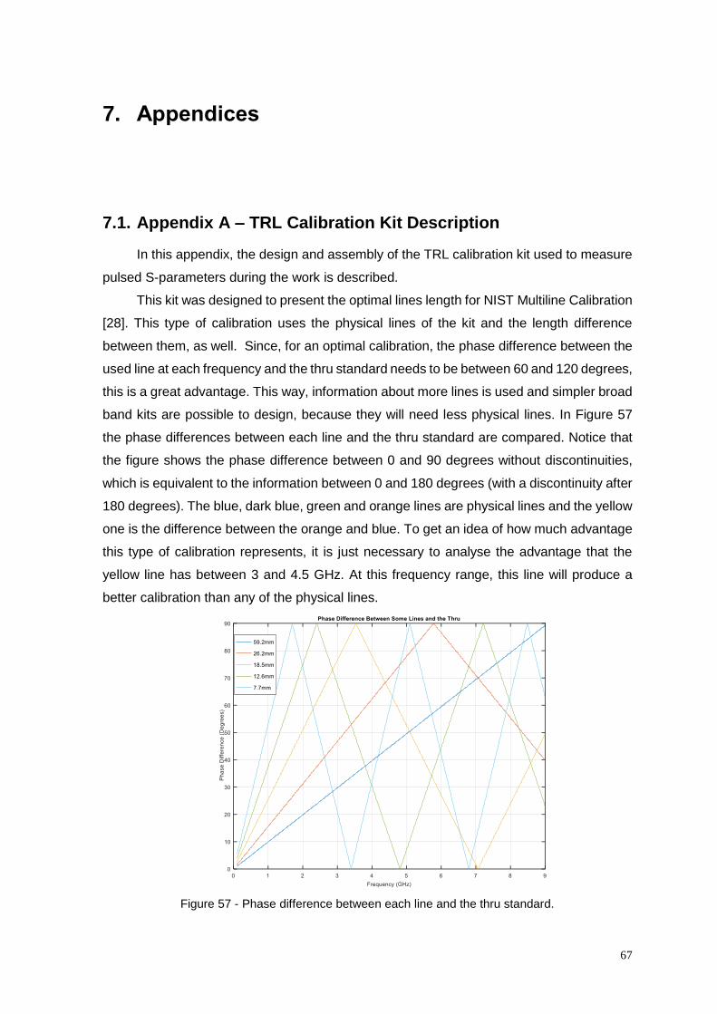
67
7. Appendices
7.1. Appendix A – TRL Calibration Kit Description
In this appendix, the design and assembly of the TRL calibration kit used to measure
pulsed S-parameters during the work is described.
This kit was designed to present the optimal lines length for NIST Multiline Calibration
[28]. This type of calibration uses the physical lines of the kit and the length difference
between them, as well. Since, for an optimal calibration, the phase difference between the
used line at each frequency and the thru standard needs to be between 60 and 120 degrees,
this is a great advantage. This way, information about more lines is used and simpler broad
band kits are possible to design, because they will need less physical lines. In Figure 57
the phase differences between each line and the thru standard are compared. Notice that
the figure shows the phase difference between 0 and 90 degrees without discontinuities,
which is equivalent to the information between 0 and 180 degrees (with a discontinuity after
180 degrees). The blue, dark blue, green and orange lines are physical lines and the yellow
one is the difference between the orange and blue. To get an idea of how much advantage
this type of calibration represents, it is just necessary to analyse the advantage that the
yellow line has between 3 and 4.5 GHz. At this frequency range, this line will produce a
better calibration than any of the physical lines.
Figure 57 - Phase difference between each line and the thru standard.
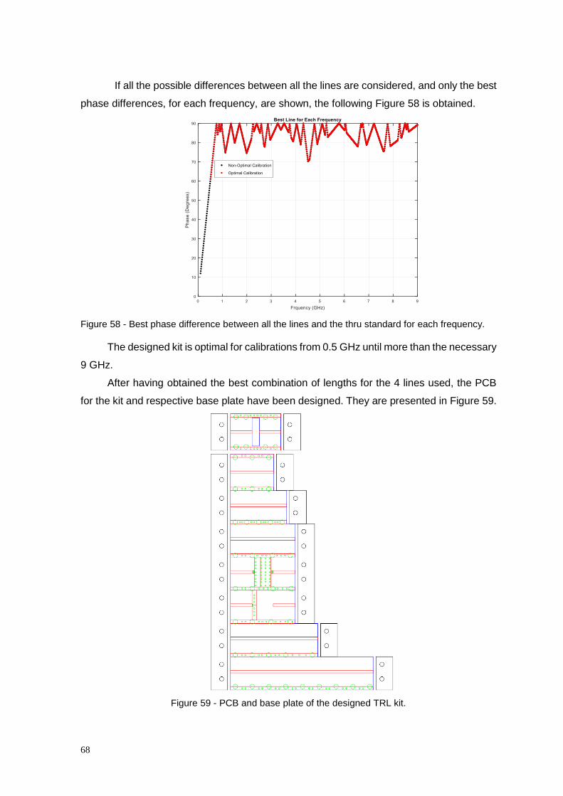
68
If all the possible differences between all the lines are considered, and only the best
phase differences, for each frequency, are shown, the following Figure 58 is obtained.
Figure 58 - Best phase difference between all the lines and the thru standard for each frequency.
The designed kit is optimal for calibrations from 0.5 GHz until more than the necessary
9 GHz.
After having obtained the best combination of lengths for the 4 lines used, the PCB
for the kit and respective base plate have been designed. They are presented in Figure 59.
Figure 59 - PCB and base plate of the designed TRL kit.

69
The red layer represents the cooper, the green one denotes the via holes used, and
the black one contains the design of the sides of the base plate, in which the PCB and the
connectors will be fixed.
The type of connectors used is very important as well. For this kit, the used
connectors, from AMPHENOL RF, are rated until 18 GHz [40], and have been tested until
10 GHz with positive results.
Figure 60 - Type of connector used.
The fact that the solder pin of the connector is flat makes it easier to solder in the
same way for every line. It is very important to have coherent connections between different
lines, especially the gap between the connector and the PCB edge, it must be exactly the
same for every line, and as smaller as possible.
After the design of the kit and the selection of the connectors, it has been assembled.
The photograph of the complete kit is shown in Figure 61.
Figure 61 - Photograph of the complete TRL kit.

70
After assembled, the kit has been measured in order to verify the quality of the
standards, namely to evaluate the losses of the open, short and lines.
Figure 62 represents the losses of the open and short standards.
Figure 62 - Open and short standards reflection values.
A reflection of -0.6 dB and -0.9 dB are the worst case for the open and short,
respectively. These values are good enough to obtain a decent calibration. In TRL
calibration the most important thing is that the value of the reflect standard (open or short)
needs to be exactly the same for the two ports of the VNA, its absolute value does not need
to be perfect.
The Figure 63 shows the transmission and reflection of one of the lines.
Figure 63 - Reflection and transmission of one of the lines.
The measured losses in the transmission are low, so as the reflection. But, more
important than that, is the fact that the reflexion reveals the typical resonances of the line
without any noise, which is very important for the calibration.