Inverse lithography as a DFM tool: accelerating design rule development with model-based assist...
10
Inverse Lithography as a DFM Tool: Accelerating Design Rule Development with Model-Based Assist Feature Placement, Fast Optical Proximity Correction and Lithographic Hotspot Detection Steve Prins a* , James Blatchford a , Simon Chang a , Lewis Flanagin a , Scott Jessen a , Sean O’Brien a , Guangming Xiao b , Timothy Lin b , Thuc Dam b , Bob Gleason b a Texas Instruments, Inc., Dallas, TX b Luminescent Technologies, Inc., Palo Alto, CA ABSTRACT Design rule (DR) development strategies were fairly straightforward at earlier technology nodes when node-on-node scaling could be accommodated easily by reduction of λ/NA. For more advanced nodes, resolution enhancement technologies such as off-axis illumination and sub-resolution assist features have become essential for achieving full shrink entitlement, and DR restrictions must be implemented to comprehend the inherent limitations of these techniques (e.g., forbidden pitches) and the complex and unanticipated 2D interactions that arise from having a large number of random geometric patterns within the optical ambit. To date, several factors have limited the extent to which 2D simulations could be used in the DR development cycle, including exceedingly poor cycle time for optimizing OPC and SRAF placement recipes per illumination condition, prohibitively long simulation time for characterizing the lithographic process window on large 2D layouts, and difficulty in detecting marginal lithographic sites using simulations based on discrete cut planes. We demonstrate the utility of the inverse lithography technology technique [1] to address these limitations in the novel context of restrictive DR development and design for manufacturability for the 32nm node. Using this technique, the theoretically optimum OPC and SRAF treatment for each layout are quickly and automatically generated for each candidate illumination condition, thereby eliminating the need for complex correction and placement recipes. “Ideal” masks are generated to explore physical limits and subsequently “Manhattanized” in accordance with mask rules to explore realistic process limits. Lithography process window calculations are distributed across multiple compute cores, enabling rapid full-chip-level simulation. Finally, pixel-based image evaluation enables hot-spot detection at arbitrary levels of resolution, unlike the ‘cut line’ approach. We have employed the ILT technique to explore forbidden-pitch contact hole printing in random logic. Simulations from cells placed in random context are used to evaluate the effectiveness of restricting pitches in contact hole design rules. We demonstrate how this simulation approach may not only accelerate the design rule development cycle, but also may enable more flexibility in design by revealing overly restrictive rules, or reduce the amount of hot-spot fixing required later in the design phase by revealing where restrictions are needed. Keywords: OPC, design rule, lithography simulation, contact holes *[email protected] Design for Manufacturability through Design-Process Integration II, edited by Vivek K. Singh, Michael L. Rieger, Proc. of SPIE Vol. 6925, 69250E, (2008) · 0277-786X/08/$18 · doi: 10.1117/12.774581 Proc. of SPIE Vol. 6925 69250E-1 2008 SPIE Digital Library -- Subscriber Archive Copy
-
Upload
independent -
Category
Documents
-
view
2 -
download
0
Transcript of Inverse lithography as a DFM tool: accelerating design rule development with model-based assist...
Inverse Lithography as a DFM Tool: Accelerating Design Rule Development with Model-Based Assist Feature Placement, Fast Optical Proximity Correction and Lithographic Hotspot Detection
Steve Prinsa*, James Blatchforda, Simon Changa, Lewis Flanagina, Scott Jessena, Sean O’Briena, Guangming Xiaob, Timothy Linb, Thuc Damb, Bob Gleasonb
a Texas Instruments, Inc., Dallas, TX
bLuminescent Technologies, Inc., Palo Alto, CA
ABSTRACT
Design rule (DR) development strategies were fairly straightforward at earlier technology nodes when node-on-node scaling could be accommodated easily by reduction of λ/NA. For more advanced nodes, resolution enhancement technologies such as off-axis illumination and sub-resolution assist features have become essential for achieving full shrink entitlement, and DR restrictions must be implemented to comprehend the inherent limitations of these techniques (e.g., forbidden pitches) and the complex and unanticipated 2D interactions that arise from having a large number of random geometric patterns within the optical ambit.
To date, several factors have limited the extent to which 2D simulations could be used in the DR development cycle, including exceedingly poor cycle time for optimizing OPC and SRAF placement recipes per illumination condition, prohibitively long simulation time for characterizing the lithographic process window on large 2D layouts, and difficulty in detecting marginal lithographic sites using simulations based on discrete cut planes. We demonstrate the utility of the inverse lithography technology technique [1] to address these limitations in the novel context of restrictive DR development and design for manufacturability for the 32nm node. Using this technique, the theoretically optimum OPC and SRAF treatment for each layout are quickly and automatically generated for each candidate illumination condition, thereby eliminating the need for complex correction and placement recipes. “Ideal” masks are generated to explore physical limits and subsequently “Manhattanized” in accordance with mask rules to explore realistic process limits. Lithography process window calculations are distributed across multiple compute cores, enabling rapid full-chip-level simulation. Finally, pixel-based image evaluation enables hot-spot detection at arbitrary levels of resolution, unlike the ‘cut line’ approach.
We have employed the ILT technique to explore forbidden-pitch contact hole printing in random logic. Simulations from cells placed in random context are used to evaluate the effectiveness of restricting pitches in contact hole design rules. We demonstrate how this simulation approach may not only accelerate the design rule development cycle, but also may enable more flexibility in design by revealing overly restrictive rules, or reduce the amount of hot-spot fixing required later in the design phase by revealing where restrictions are needed.
Keywords: OPC, design rule, lithography simulation, contact holes *[email protected]
Design for Manufacturability through Design-Process Integration II, edited by Vivek K. Singh, Michael L. Rieger, Proc. of SPIE Vol. 6925, 69250E, (2008) · 0277-786X/08/$18 · doi: 10.1117/12.774581
Proc. of SPIE Vol. 6925 69250E-12008 SPIE Digital Library -- Subscriber Archive Copy
1. INTRODUCTION Just a few process technology nodes ago, the task of defining next-generation design rules did not require the analysis of data from hundreds of thousands of lithography simulations. Over the last few nodes, due to much smaller k1 factors and subsequent extensive use of resolution enhancement technologies, design rule complexity has increased immensely. The lithography simulations required to support the establishment of design rules have correspondingly increased, and now include more extensive two dimensional (2D) simulations to explore a multitude of restrictive design rules.
Simulations of 2D, parameterized, structures are paramount for refining design rules; however, simulations of actual logic layouts are becoming more important for understanding the complex interaction of 2D design restrictions. As designers begin to lay out core cells, early feedback to identify marginal lithographic sites may enable further design rule refinement and corrections before the full ramp in cell layout begins. Ideally, cells are simulated in a variety of random contextual placements to explore unanticipated interactions arising from an optical ambit that now extends far past cell boundaries.
Several factors in the simulation flow have limited the extent to which data could be generated from 2D simulations, particularly simulations of cells in random context. These factors include long computation times, limited analysis capabilities, and complexity of setting up optical proximity correction (OPC) and sub resolution assist feature (SRAF) recipes. This paper discusses the how a simulation tool employing inverse lithography technology (ILT) was used to address these limiting factors for simulations in support of next-generation design rule definition. We demonstrate its utility with a study of contact hole printing.
A very well-known consequence of using annular illumination in contact hole printing is the existence of “forbidden pitch” regions [2], typically demonstrated with data from through-pitch gridded hole layout. We investigate the lithographic performance of holes placed at forbidden pitches in random logic. We do this on a hole-by-hole basis for several cells placed in a random context. The lithography performance of holes at forbidden pitches in gridded layout is shown to be different from holes at forbidden pitches in random logic.
2. METHODOLOGY 2.1 Inverse lithography as a simulation tool
Luminescent’s Luminizer LE lithography simulation tool has been used to address several of the limiting factors in the simulation flow. It uses a distributed computing hardware platform to address the issue of long computation time. Its use of pixel-based analysis and automated placement of metrology “topologies” [1] to cover all pattern feature types ensures that all marginal lithographic spots will be identified. Finally it addresses the complexity of OPC and SRAF recipe setup with its incorporation of ILT.
A significant part of the lithography “problem” for critical patterning levels is to determine what pattern must be placed on a photomask to reproduce the desired target pattern on the wafer. Traditional methods used for solving this problem involved several steps. First, for a given illumination condition, a model that provides a mask-to-wafer transformation function must be calibrated from thru-pitch SEM data or, for early in the development cycle, from data generated by a lithography simulation tool. Next, SRAF placement tables dependent on illumination condition must be formulated; this typically involves careful analysis of a large number of thru-pitch lithography simulations. Finally, OPC and SRAF placement recipes must be created, most likely requiring the support of engineers trained on an EDA software platform.
The ILT “inversion recipes” are generally much easier to set up than OPC recipes, especially in cases where incorporation of sub resolution assist features (SRAFs) is desired. ILT not only simplifies the mask definition problem, but may offer better solutions. Typical OPC software begins by segmenting the targeted geometries and subsequently moving these segments iteratively to achieve the targeted pattern. Alternatively, ILT solves the problem, or performs the inversion, by formulating a rigorous mathematical framework that explores a solution space independent of the original target data. The solution is considered an ideal freeform mask and consists of smooth contours. Subsequent “Manhattanization,” where the smooth mask profiles are reshaped to more traditional Manhattan skyline look, is required to render the mask manufacturable.
These enabling factors, along with the software’s capability to perform depth of focus (DOF) and mask error enhancement factor (MEEF) calculations, enforce mask rules, and vary illumination conditions have provided tooling necessary for performing many random logic simulations with a reasonable effort.
Proc. of SPIE Vol. 6925 69250E-2
300 5MEEFBudget
250 4 4.5
200 3m
0 m'1150 2
DOFBudget 100 1
lOOnm
50 0100 150 200 250 300 350
Pitch (nm)
2.2 Forbidden pitches in contact hole printing
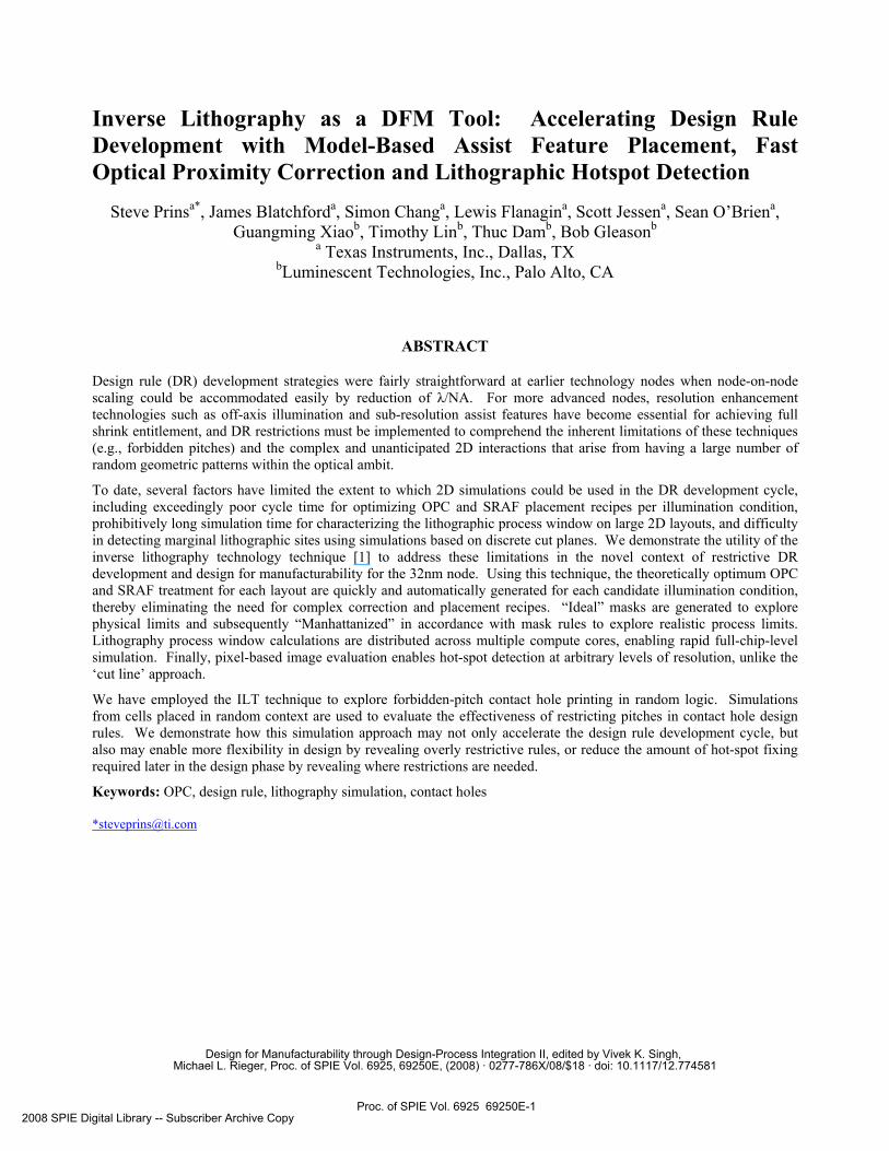
Annular illumination may be used for contact hole printing to accommodate both tight pitches and off-grid hole placement. However, this illumination scheme results in “forbidden pitch” (FP) regions in the gridded-hole pitch spectrum marked by poor DOF and MEEF. Aerial image simulations of DOF (5% exposure latitude) and MEEF (+/-2nm mask bias) as a function of pitch for gridded contact holes are shown in Figure 1. These simulations were performed at 1.35NA with annular illumination (0.65/0.85), XY polarization, and 6% attenuated phase-shifting masks. In the region identified with cross-hatch, poor DOF in the lower end of the region occurs when neighboring holes begin to diminish their diffractive support and SRAFs will not yet fit in the space between the holes because of limitations in mask making. The spike in MEEF occurs at the point where SRAFs will fit; high-density patterns typically exhibit higher MEEF.
DOF and MEEF budgets partially dictate the potential severity of critical dimension (CD) control issues. Given typical DOF budgets for the 32nm node, design rules for restricting placement of holes at forbidden pitches may be necessary. In the example shown in Figure 1, a 100nm DOF budget and 4.5 MEEF budget may lead to a conclusion that layout restrictions will be required for hole pitches between ~150nm and ~190nm. However, typical contact hole placement in random logic is not gridded and may therefore show very different lithographic performance than what is shown in the figure. This is the motivation for the experiments that are described.
Fig. 1. DOF and MEEF thru pitch for annularly illuminated contact hole patterns through pitch. The first “forbidden pitch”
region is defined with cross-hatched area and includes pitches with poor DOF and/or MEEF margin.
2.3 Experiment
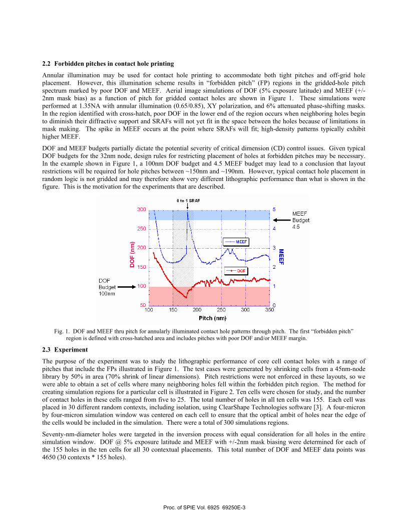
The purpose of the experiment was to study the lithographic performance of core cell contact holes with a range of pitches that include the FPs illustrated in Figure 1. The test cases were generated by shrinking cells from a 45nm-node library by 50% in area (70% shrink of linear dimensions). Pitch restrictions were not enforced in these layouts, so we were able to obtain a set of cells where many neighboring holes fell within the forbidden pitch region. The method for creating simulation regions for a particular cell is illustrated in Figure 2. Ten cells were chosen for study, and the number of contact holes in these cells ranged from five to 25. The total number of holes in all ten cells was 155. Each cell was placed in 30 different random contexts, including isolation, using ClearShape Technologies software [3]. A four-micron by four-micron simulation window was centered on each cell to ensure that the optical ambit of holes near the edge of the cells would be included in the simulation. There were a total of 300 simulations regions.
Seventy-nm-diameter holes were targeted in the inversion process with equal consideration for all holes in the entire simulation window. DOF @ 5% exposure latitude and MEEF with +/-2nm mask biasing were determined for each of the 155 holes in the ten cells for all 30 contextual placements. This total number of DOF and MEEF data points was 4650 (30 contexts * 155 holes).
Proc. of SPIE Vol. 6925 69250E-3
cell cell
a b
— 4 jtm —•
cellEc
METHOD 1 METHOD2Shifted Tolerance Window
Target Nominal Contours t(e.g. 71.5nm)
140
120
IOU
Hole
60 1 - -
40 10 .....• 11• 12
20 • 13
'a holesx Oco'itextsxZ cells36O holes)
Tolerance Window-1'
Target 7Onm "Drawn" CD
140
120
IOU
90
60
40
20
fl
- - -- -
05•10- - - - -. --* 11• 12
13 - - -
la
Max Edge Placement Eor (nm)1
ECLI-00
IMax Edge Placement Eor (nm)I 1:
Fig. 2. Core cell simulation setup: a) cell, b) placed in random contexts, 6 shown, and c) 4-micron by 4-micron regions
extracted for lithography simulation.
3. DATA, ANALYSIS AND RESULTS 3.1 Hole targeting and DOF simulations
Similar to all techniques for optimizing the mask pattern, the inversion process does not achieve perfect targeting for all holes in the simulation region. Therefore, even under nominal focus and dose conditions, one or more of the four sides (left/right/up/down) of all holes will print with a non-zero targeting error. This is due to mask grid snapping combined with high MEEF and to limitations of the inversion process: an inversion targeting tolerance is allowed to ensure the inversion process completes in a reasonable time. Under nominal focus and dose conditions, the maximum edge placement error (EPE) for hole targeting was found to be three times higher, on average, for random logic than for gridded hole patterns through pitch. This observation suggests that hole targeting in the 32nm node may be a significant issue if the mask database unit is not sufficiently small.
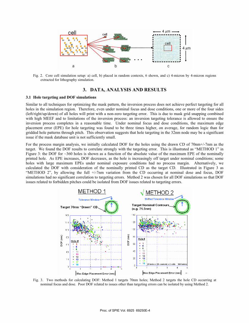
For the process margin analysis, we initially calculated DOF for the holes using the drawn CD of 70nm+/-7nm as the target. We found the DOF results to correlate strongly with the targeting error. This is illustrated as “METHOD 1” in Figure 3: the DOF for ~360 holes is shown as a function of the absolute value of the maximum EPE of the nominally printed hole. As EPE increases, DOF decreases, as the hole is increasingly off target under nominal conditions; some holes with large maximum EPEs under nominal exposure conditions had no process margin. Alternatively, we calculated the DOF with consideration of the nominally printed CD as the target CD. Illustrated in Figure 3 as “METHOD 2”, by allowing the full +/-7nm variation from the CD occurring at nominal dose and focus, DOF simulations had no significant correlation to targeting errors. Method 2 was chosen for all DOF simulations so that DOF issues related to forbidden pitches could be isolated from DOF issues related to targeting errors.
Fig. 3. Two methods for calculating DOF: Method 1 targets 70nm holes; Method 2 targets the hole CD occurring at
nominal focus and dose. Poor DOF related to issues other than targeting errors can be isolated by using Method 2.
Proc. of SPIE Vol. 6925 69250E-4
200 250 300
Pitch (nm)
.1. ci• .!.II'•..
S........0.I •• . S
FP1 = "Rectangular Grid" FP2 = "Checkerboard Grid"
125
ES 100LI-00
75
3.2 Hole binning: consideration of two forbidden pitch regions
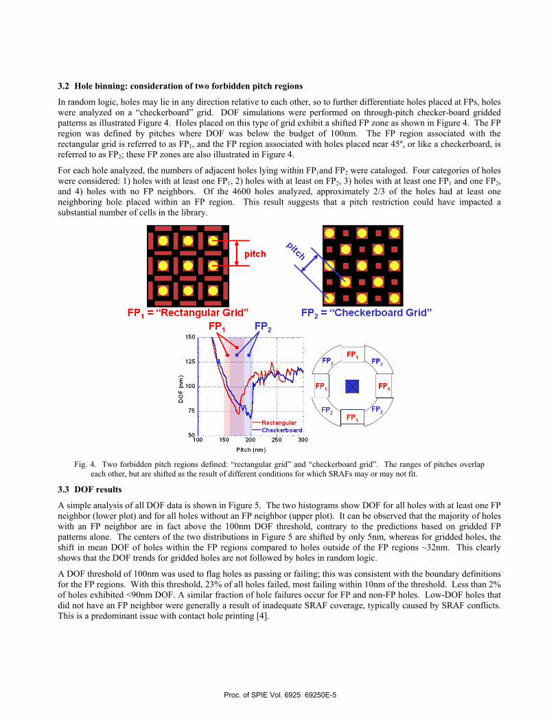
In random logic, holes may lie in any direction relative to each other, so to further differentiate holes placed at FPs, holes were analyzed on a “checkerboard” grid. DOF simulations were performed on through-pitch checker-board gridded patterns as illustrated Figure 4. Holes placed on this type of grid exhibit a shifted FP zone as shown in Figure 4. The FP region was defined by pitches where DOF was below the budget of 100nm. The FP region associated with the rectangular grid is referred to as FP1, and the FP region associated with holes placed near 45º, or like a checkerboard, is referred to as FP2; these FP zones are also illustrated in Figure 4.
For each hole analyzed, the numbers of adjacent holes lying within FP1and FP2 were cataloged. Four categories of holes were considered: 1) holes with at least one FP1, 2) holes with at least on FP2, 3) holes with at least one FP1 and one FP2, and 4) holes with no FP neighbors. Of the 4600 holes analyzed, approximately 2/3 of the holes had at least one neighboring hole placed within an FP region. This result suggests that a pitch restriction could have impacted a substantial number of cells in the library.
Fig. 4. Two forbidden pitch regions defined: “rectangular grid” and “checkerboard grid”. The ranges of pitches overlap
each other, but are shifted as the result of different conditions for which SRAFs may or may not fit.
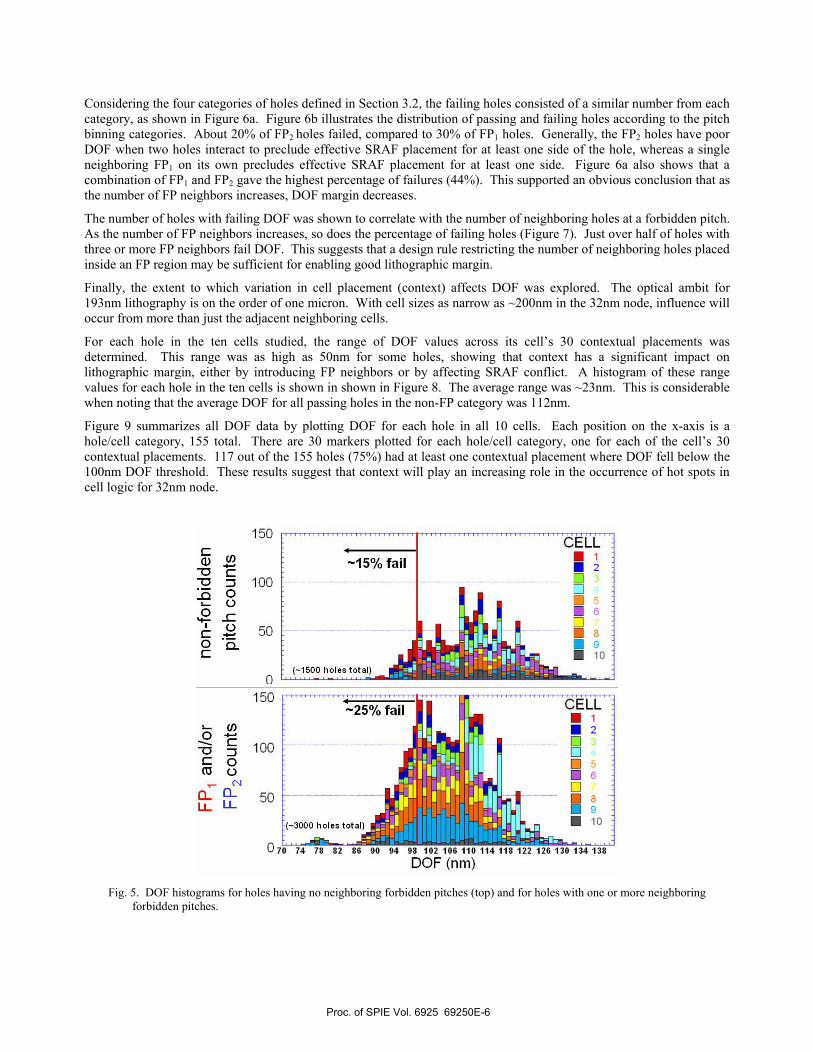
3.3 DOF results
A simple analysis of all DOF data is shown in Figure 5. The two histograms show DOF for all holes with at least one FP neighbor (lower plot) and for all holes without an FP neighbor (upper plot). It can be observed that the majority of holes with an FP neighbor are in fact above the 100nm DOF threshold, contrary to the predictions based on gridded FP patterns alone. The centers of the two distributions in Figure 5 are shifted by only 5nm, whereas for gridded holes, the shift in mean DOF of holes within the FP regions compared to holes outside of the FP regions ~32nm. This clearly shows that the DOF trends for gridded holes are not followed by holes in random logic.
A DOF threshold of 100nm was used to flag holes as passing or failing; this was consistent with the boundary definitions for the FP regions. With this threshold, 23% of all holes failed, most failing within 10nm of the threshold. Less than 2% of holes exhibited <90nm DOF. A similar fraction of hole failures occur for FP and non-FP holes. Low-DOF holes that did not have an FP neighbor were generally a result of inadequate SRAF coverage, typically caused by SRAF conflicts. This is a predominant issue with contact hole printing [4].
Proc. of SPIE Vol. 6925 69250E-5
150 [L •MMVi• ••il
—15% failCci)-D-D-D0C0C
100
50
0
LtLL•iUU
• •5InI U- • 8•9•1o
(—1500 holes total)
150
100
50
.— U)0—— C-D jCO(oN
Li-u-
07p 14 1 Z SO 90 94 95 1VZ 1kw 110 114 110 12Z 1Z0 US IM 130
DOF (nm)
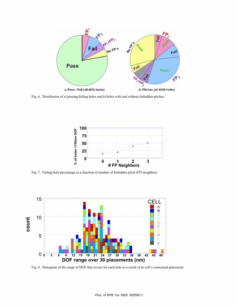
Considering the four categories of holes defined in Section 3.2, the failing holes consisted of a similar number from each category, as shown in Figure 6a. Figure 6b illustrates the distribution of passing and failing holes according to the pitch binning categories. About 20% of FP2 holes failed, compared to 30% of FP1 holes. Generally, the FP2 holes have poor DOF when two holes interact to preclude effective SRAF placement for at least one side of the hole, whereas a single neighboring FP1 on its own precludes effective SRAF placement for at least one side. Figure 6a also shows that a combination of FP1 and FP2 gave the highest percentage of failures (44%). This supported an obvious conclusion that as the number of FP neighbors increases, DOF margin decreases.
The number of holes with failing DOF was shown to correlate with the number of neighboring holes at a forbidden pitch. As the number of FP neighbors increases, so does the percentage of failing holes (Figure 7). Just over half of holes with three or more FP neighbors fail DOF. This suggests that a design rule restricting the number of neighboring holes placed inside an FP region may be sufficient for enabling good lithographic margin.
Finally, the extent to which variation in cell placement (context) affects DOF was explored. The optical ambit for 193nm lithography is on the order of one micron. With cell sizes as narrow as ~200nm in the 32nm node, influence will occur from more than just the adjacent neighboring cells.
For each hole in the ten cells studied, the range of DOF values across its cell’s 30 contextual placements was determined. This range was as high as 50nm for some holes, showing that context has a significant impact on lithographic margin, either by introducing FP neighbors or by affecting SRAF conflict. A histogram of these range values for each hole in the ten cells is shown in shown in Figure 8. The average range was ~23nm. This is considerable when noting that the average DOF for all passing holes in the non-FP category was 112nm.
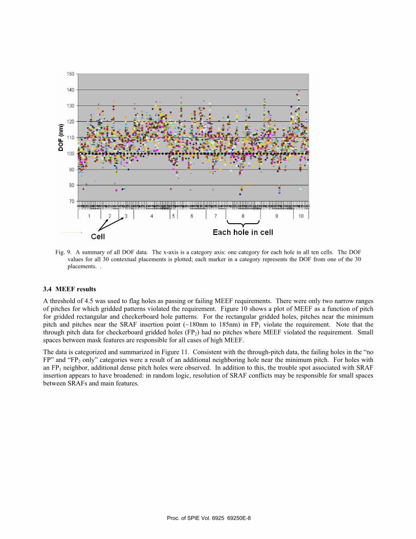
Figure 9 summarizes all DOF data by plotting DOF for each hole in all 10 cells. Each position on the x-axis is a hole/cell category, 155 total. There are 30 markers plotted for each hole/cell category, one for each of the cell’s 30 contextual placements. 117 out of the 155 holes (75%) had at least one contextual placement where DOF fell below the 100nm DOF threshold. These results suggest that context will play an increasing role in the occurrence of hot spots in cell logic for 32nm node.
Fig. 5. DOF histograms for holes having no neighboring forbidden pitches (top) and for holes with one or more neighboring
forbidden pitches.
Proc. of SPIE Vol. 6925 69250E-6
ft.
Pass
a. Pass I Fail (all 4600 holes) b. Pitches (all 4600 holes)
Fig. 6. Distribution of a) passing/failing holes and b) holes with and without forbidden pitches.
0
25
50
75
100
0 1 2 3% o
f hol
es <
100n
m D
OF
# FP Neighbors Fig. 7. Failing hole percentage as a function of number of forbidden pitch (FP) neighbors.
0
5
10
15
0 3 6 9 12 15 18 21 24 27 30 33 36 39 42 45 48
ABCDEFGHIJ
coun
t
DOF range over 30 placements (nm)
CELL
Fig. 8. Histogram of the range of DOF that occurs for each hole as a result of its cell’s contextual placement.
Proc. of SPIE Vol. 6925 69250E-7
150
140
130
120
EC
110
0aIOU
90
80
70
Each hole in cellCell
Fig. 9. A summary of all DOF data. The x-axis is a category axis: one category for each hole in all ten cells. The DOF
values for all 30 contextual placements is plotted; each marker in a category represents the DOF from one of the 30 placements. .
3.4 MEEF results
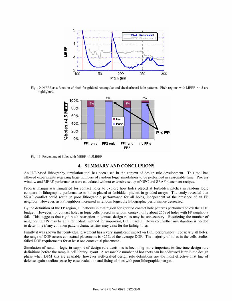
A threshold of 4.5 was used to flag holes as passing or failing MEEF requirements. There were only two narrow ranges of pitches for which gridded patterns violated the requirement. Figure 10 shows a plot of MEEF as a function of pitch for gridded rectangular and checkerboard hole patterns. For the rectangular gridded holes, pitches near the minimum pitch and pitches near the SRAF insertion point (~180nm to 185nm) in FP1 violate the requirement. Note that the through pitch data for checkerboard gridded holes (FP2) had no pitches where MEEF violated the requirement. Small spaces between mask features are responsible for all cases of high MEEF.
The data is categorized and summarized in Figure 11. Consistent with the through-pitch data, the failing holes in the “no FP” and “FP2 only” categories were a result of an additional neighboring hole near the minimum pitch. For holes with an FP1 neighbor, additional dense pitch holes were observed. In addition to this, the trouble spot associated with SRAF insertion appears to have broadened: in random logic, resolution of SRAF conflicts may be responsible for small spaces between SRAFs and main features.
Proc. of SPIE Vol. 6925 69250E-8
:MEEF (Rectangular)
100 150 200 250 300
Pitch (nm)
%ho
les
>4.
5 M
EE
F
a 0)
0
0 0
0 0
0 0
-u
A
m
-u
UI
Fig. 10. MEEF as a function of pitch for gridded rectangular and checkerboard hole patterns. Pitch regions with MEEF > 4.5 are
highlighted.
Fig. 11. Percentage of holes with MEEF <4.5MEEF
4. SUMMARY AND CONCLUSIONS An ILT-based lithography simulation tool has been used in the context of design rule development. This tool has allowed experiments requiring large numbers of random logic simulations to be performed in reasonable time. Process window and MEEF performance were calculated without extensive set up of OPC and SRAF placement recipes.
Process margin was simulated for contact holes to explore how holes placed at forbidden pitches in random logic compare in lithographic performance to holes placed at forbidden pitches in gridded arrays. The study revealed that SRAF conflict could result in poor lithographic performance for all holes, independent of the presence of an FP neighbor. However, as FP neighbors increased in random logic, the lithographic performance decreased.
By the definition of the FP region, all patterns in that region for gridded contact hole patterns performed below the DOF budget. However, for contact holes in logic cells placed in random context, only about 25% of holes with FP neighbors fail. This suggests that rigid pitch restriction in contact design rules may be unnecessary. Restricting the number of neighboring FPs may be an intermediate method for improving DOF margin. However, further investigation is needed to determine if any common pattern characteristics may exist for the failing holes.
Finally it was shown that contextual placement has a very significant impact on DOF performance. For nearly all holes, the range of DOF across contextual placements is ~25% of the average DOF. The majority of holes in the cells studies failed DOF requirements for at least one contextual placement.
Simulation of random logic in support of design rule decisions is becoming more important to fine tune design rule definitions before the ramp in cell library layout. A reasonable number of hot spots can be addressed later in the design phase when DFM kits are available, however well-crafted design rule definitions are the most effective first line of defense against tedious case-by-case evaluation and fixing of sites with poor lithographic margin.
Proc. of SPIE Vol. 6925 69250E-9

REFERENCES
[1] S. Abrams, et al., “Fast inverse lithography technology,” Proc. SPIE 6154 (2006). [2] R. Socha, et al., “Forbidden Pitches for l30nm lithography and below,” Proc. SPIE 4000, p.1140 (2000). [3] Darsun Tsien, et al., “Context-specific leakage and delay analysis of a 65nm standard cell library for lithography-
induced variability,” Proc. SPIE 6521 (2007). [4] S. Jessen, et al., “Design rule considerations for 65-nm node contact using off axis illumination,” Proc. SPIE 5756
(2005).
Proc. of SPIE Vol. 6925 69250E-10