TITLE TITLE TITLE TITLE TITLE TITLE TITLE TITLE ... - EconStor
Upload
independentCategory
view
0download
0
Resist deposition without spinning by using novel inkjettechnology and direct lithography for MEMS
Gökhan Perçin, Tom H. Soh, and Butrus T. Khuri-Yakub
Edward L. Ginzton Laboratory, Stanford University, Stanford, CA 94305-4085
ABSTRACTThis article presents a technique for resist deposition using a novel fluid ejection method. An ejector has beendeveloped to deposit photoresist on silicon wafers without spinning. Drop-on-demand coating of the wafer reduceswaste and the cost of coating wafers. The novel piezoelectric fluid ejector is based on a variation of the design ofa flextensional transducer that excites axisymmetric resonant modes in a clamped circular membrane. The ejectoris made by bonding a thin piezoelectric ring to a thin, fully supported, circular membrane. The ejector design isoptimized for maximum flexure at the lowest order resonant frequency using finite element modeling. The resist isplaced behind one face of the membrane which has a small orifice (50-150 im diameter) in its center. By applying anac signal across the piezoelectric element, continuous or drop-on-demand ejection of the resist is achieved. Shipley1400-21, 1400-27, 1805, and 1813 resists were used to coat sample 3" wafers. Later, these wafers were exposed anddeveloped. The deposited resist film was 3.5 im thick and had a surface roughness of about 0.2 m. The ultimategoal is to deposit resist films with a thickness of the order of 0.5 ,um, and a surface roughness of the order of 30 A°.Such goals can be attained by using micromachined multiple ejectors presently under development, or with bettercontrol over the deposition environment. In the micromachined configuration, thousands of ejectors will be madeinto a silicon die and thus allow for full coating of a wafer in a few seconds. Coating in a clean environment willallow the lithography of circuits for microelectronic applications.
Keywords: Photoresist, resist deposition, resist dispenser, coating, lithography, MEMS, ink jet.
1. INTRODUCTIONLithography is the leading step in microelectronics technology. Photoresist coating is the one of the expensive stepsin the lithography process. The photoresist film, after application to the substrate, must have uniform thickness andmust be chemically isotropic so that its response to exposure and development is uniform. In the literature, severaltypes of photoresist coating methods are reported1'2: spin coating, spray coating, dip coating, meniscus coating,plasma-deposited photoresist , electrodeposited (electrophoretic) photoresist , and roller , curtain and extrusion coat-ing. However, spin coating remains the method of choice of the microelectronic industry. In present applications,over 95% of the photoresist is wasted and has to be disposed of as a toxic material, thus making this one of themore expensive steps in integrated circuit manufacturing. Especially, radial thickness variations associated with theapplication of photoresist by spinning must be avoided. The origin of the potential variations in physical propertiesof the photoresist film lies in the spin coating technique. Large amounts of extra free volume are trapped in the filmduring the spin coating.
The device we developed uses a drop-on-demand method to dispense photoresist on wafers. Drop-on-demandcoating of the wafers reduces the waste and the cost of coating wafers. In addition to reducing waste, this methodcan be used to coat odd-shaped substrates (i.e. flat panel displays), to planarize the resist profile on the wafers(i.e. putting more resist on some parts of the wafers), to finely control its spatial distribution in real-time, topossibly reduce the use of HMDS, and to do direct write for micro electromechanical systems (MEMS) where criticaldimensions are in the order of several microns. The novel piezoelectric fluid ejector can find applications in integratedcircuit manufacturing not only for photoresist coating but also for dispensing chemicals to desired regions. The ejectoris harmless to sensitive fluids. The method also opens new possibilities, e.g., intentionally varying the resist thicknessacross the wafer.
Send correspondence to G P., e-mail: percin©alumni stanford .org, homepage: http://www.stanfordedu/-'percin
1382 ISPIE Vol. 3333 0277-786X198/$1O.OO
Liquid
Housing
Membrane Orifice Pie zoe le ctri c
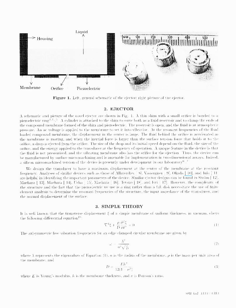
Figure 1. 1_eli general ileiii;itie of tin elector: right io(tlii(' of I in' e]e(toi.
2. EJECTORA s(iieiliat Ic 111(1 picture of the iiovei elector are shown in Fig. l.A tinti siiitii vithi a siiiali orifice is I )iidd apii'Zii('(tiiC 1111gJ .' A i'vliiidei is attacii('d to tue slain to seiv' both as i 11111(1 reservoir aid to cianiii I in' ends oftue conipound nienihrane f'ornied of tiii' slant and pii'zo('lect rn. I in' reservoir is open. atni tin' fluid is iii at nh spfieiicpressure. An lU voltage is applied to tile mcml train to set into viieat not ..\t the resonant fr'tlh'iii's of tue fluidIoad('d (o1111)otliid Iiieliihrali('. the ihspiaci'iiii'iii iii tin' 'enter is large. Tin' fhnd heiiiiol in' orihi'e is a ('celel at I'd ISthe memhraiii' is moving, and when I he in('rtlal force is larger titan tin smtrfo'e tension hue t fiat itohis it to t heorifice, a (froji is ejected front tin' orifice. Tin' sue of tin' drop ;imnl its unit ial S1H'e(l (h'p('li(i on tin' final, liii' sue of tin'orifice. and hue energy applied to tin t ransdiii'er at tin freqin'ncv of operat loll A iulliqiue h'atuire in tin (i('vi'(' 15 t Intl
the fluid is not pressurized. amid tin' vibrating nn'inhrain' also has tin' orifice for tin elect intu. i'hiis, in' h'vici' ('anin' ituatitufactured liv surface niicrotnai'huioiug and us aiin'nahii' for it.iupiemnemutliuoiu iii two-diniemisuoiial arrays. imudei'd.a i1icoii luii('iOnil('i1iIied version of tin' deviu' is presently iimii1'u devt'lopiin'iit in our lahor:itoiv"
Vie (i('siglu t lie transducer to have a iuiaXimiuiuiuu displacemuietit at tin' ('inter of the nuetiulu ;un' at tin' ri'soiuamitf'reqin'iov.Atialvses of sinuilar (ievi('es such as those (if Allaverdi'v ] s, \'assergisei tI(, ( )kadi [ 10]. aol liulo I ii
ire helpful itt ich'ntif'viiig liii' lilipirtalut pai'atiieters (it tin' device. iiuiiilr ejector desigmis ian in' found in t rdin[ I 2.Maeiiara 1 13]. Maehara [ ii), Ieiia l.. 1aeiiara ] Ib]. ietsiio [ IH. aol ivri : 7]. lloweve , the i'omiuiiiextv of
tin' structur(' and the fact that till' pi'zoeh'ctro' we use is a ring rat hit t loin a hull hsk in'cessit ate the use of footei'lenuent analysis to di'teriiuiiie the resoiuaiut freqin'mn'ies if the st nature. the input niipedaio'e of tin' t r:uusdun'ei ooithe normal (hspla('elllent of i fun surface.
3. SIMPLE THEORYIt is well kmnwtu that the transverse dlsplacelhuent of i simple itietiubramie of uunuforiii t liueiciiess, in vaciuluni, oin'vsI lie foliowi ug dii i'ere otial r'qtmat loni 5:
The axisvluiiiiet tic free vihratiomu frequencies tot in 'dge_ciatnu'd circular tin'iuibrain' ale given by
('2)(I-
where \ represents t in' i'lgen\'ahn's of Equal ion (1). o is the i;idiiis of the annul rain', p is liii' mass pci unit ani 'ii
the iuiemni (rain, and
/) -12(1 -
where E us \'oumug's nnjdiihis, Ii is t he nn'mnhrane t hiekin'ss. and a is Poisson s mat to.
P1! \'o/. 1H I 18 1
'M 0 0 0 4 I)-
' Uu\ui
i'i;itIiiiiiiiiliiii nil/i!

The above equations suggest that the resonant frequency is directly proportional to the thickness of the membraneand inversely proportional to the square of the radius. However, it is also known that the resonant frequency will bedecreased by fluid loading on one or both sides of the membrane. The shift in the fluid loaded resonant frequency ofa simple membrane is shown to be2°
fw=1F (4)
where 3 = pwa/pmh 5 a thickness correction factor, Pw 5 the density of the liquid, Pm 15 the mass density ofthe circular membrane, and F is the non-dimensional added virtual mass incremental (NAVMI) factor, which isdetermined by boundary conditions and mode shape. For the first order axisymmetric mode and for water loadingon one side of the membrane, F is 0.746313. Assuming the composite will behave similarly to the single membrane,we expect the resonant frequency to shift down by 52% for one of our devices.
The ejector orifice vibrates at a frequency f and a capillary wave of wavelength A is setup on the liquid jet.The operating frequency of the device, f, and the wavelength of the capillary wave, A, are related by the Kelvin
222
,\ =3 \/ (5)
where a and p are the surface tension of the liquid and the density of the liquid, respectively. This wave travels inthe direction of the liquid jet with a velocity of u given by
u= (6)
where k is the wave number. It is also known that to be effective for controlling the breakup of a jet wuth radius a,and a capillary wave of wavelength A must yield the nondimensional wavenumber k0 = 2ira/A with a value less than1.
Another crucial point in the theory is the spreading of photoresist drops on the wafers. There is a wide range ofliterature on this topic, and can be found in Bauer [ 23], Shikhmurzaev [ 24], Yarin [ 25], Mundo [ 26], Davis { 27],and Pasandideh-Fard { 28].
ANSYS 5.2 ..NSYS 5.2DEC 1 1995 DEC 1 199514:27:18 14:28:19DISPLCD84E]8T DISPLACEIIENT
SUB 1 DUD —2FDEQ—26D4 FDEQ12O51USD8—S USSS—TDlix —553.001 D1VD —569.961
DSCA—. 442E—06 USCA—. 259E06
DIST.OS2S48 DIDT—.SD2448SF —. 552275 UF —.002275SF —. 9875—04 IF —.609E—04
Figure 2. ANSYS simulation of the first two resonant modes of the ejector.
4. EJECTOR FABRICATION AND MODELINGWe use ANSYS, a finite element analysis commercial code, to find the resonant frequency and displacement of thecomposite transducer in vacuum. We use brass shim, steel shim, and silicon membrane as a membarane and Murata
1384 / SPIE Vol. 3333

Motorola PZT'320311D
Murata PZT
surface wave material
Lithium niobate
'iA lO, 36 cUt
'.1I'al)1( 1. 1ro1,itti,i- of J)iP/.))e(le(t ru iiIlteIiul iisid.
PZT sijrfa,t Wave material.-1 \1otorola PZ/ 3203F1D:eJ and lit hiiiin iiiohate ( L,.V6( ),) a pie/ feetii) 0111 ilesigiis. laDle 1 I1OW the pl1vi(al I 11t)UIt Of tile pie/oeleetrl( material. liii pI(/.o(l((l 111 niateri;ik Were(lloeti because 1 for retain their 1>roIorties \vhlen polished to a thickness ol 2.i /,tn. vhien;is brass and steel sbiiiisWere (bosch h)e(ahlS( they are easily Vaikih)le. Oii the other hiaiicl. U) uSC 511001! 1,1(0111)1 ala hot to )OlllaflhiIlatethe fill toresisi evera1 iteratiohus Well' 101!) to niaxwuze t ho (llSpliOehtleIit of I lii' tiieitihiraiti I5 a 1111(1 loll of the(hilll(IiSiOIlS of t iii' piezoelc(trie ring. \Iaxmuini (Ilspl;lcehuleTlt is obtainid vhie1i the piei.oeleetric ring ( \lurata /'/ Iiii tins ease has an inner diameter of 2 nini and oilier (liahlieter of 7 11)01 for a brass shni vil Ii ii haiiietei ofP rani.
Figure 2 shows a typical result of I lie finite eleiiient analysis: naiiielv. tile vert cal (llspl;l)(hiIelIi of ha In(nhl)raneas a function of radial position. Flie F)( displaeeiiieiit at lie center iS I. l iiii/\. iiid liii' first wi, axisylnuilti icr(soIlult heqiieniies are at 2601 kHv and 12.0.i khli.
5. EXPERIMENTS AND RESULTScde model devices were fabricated uismg the opillIluillI eollfigulr;ltioll cleseri ed eailar. lie oservoir was iiade ofbrass with a height of iiini. A 2Ti /1111 thin shiiiiu was boinleil to tb /1111 iloek piei.oiIeetric rilig. lh 11111(1 oaf0111(1 ,hiaiiietirs of tile ring were 2 11110 and 7 111111 respectively. lie oifie rauiged in lianater froni pitt pin to 2))))/1111 and Was made using a drill iii a small little, or clienileal itching. lIe measured osaitalit fnquieia'v of the devicewas 2.. kIT,. iii air and 1.2 kF1 Will) tutu loading on one side. Iloth Hsall:itIl frepwines an in agrelitihit with tlii1111)1 Id predict 11)11.
.',hiplev 1 10(1-21. 1 11)11-27. 10i. 111)1 1l3 ph toresists \v(r(et(ut(d iisiiig the epclol iiialei lie ambitions hesiriledIi thii previous sictiall 1)111 with a voltage of20() \' peak to peak. ho ejected pliotoiesist drop size us at tIe orifice
l'l! Vo/ (3.3.t / 1J8
I Piezoelectric Material Density Acoustic Dielectric
Velocity Constant
1
7800 4060
QualityFactor()u
7950
3800
CouplingFactor
I, /
4709
El ectricaiLoss TangenL
/ (I I I
4640
240
30
1000
0 55 0.024
7360 39
0.48 0.014
100 0.49 0.001
F'igiirc 3. Ljcted phiotoresist droplets thou 110 ,iii liauiieter u-ih,'i.

I'1igiire 4. II11)to1'(i(iHt (ovor((l 1' \vitf('t'(.
-1'.... ....... .. ..,,..,,..,,. ..:..... .:..II II I.
I
\ l
0 '500 ''" I].)
1.11 .. .....,.,..... ..,Co
1 i-
-;
ItFiguro 5. fop. tlit oaii of UldiVillIlill p1iolou'sit lroj: bottoiti loft tb 'ui l lb olgo of tb j>1tti'it poltoril:bottom right. tb soon 11151(1) tito pliotorosist pattofli
Silt 115 sItl)WIl iii Fig. :3. w'hr (Oh)') 511) 15 1 1tPiiii. FigIlt'( -I ShOWS H(ftIill( 001tIIM of a 3 sutton ';tftt's Wit ii '1(0wastt. Tiuo l'vsist is 3.3/1111 tluirh 1111(1 has a stii Ll('o rotighirioss ((I 01)0111 (1.2 /iiui. Hgtirt SlIo\\'S pu'ohibolll)l)r (;,Ij)fia-
500115 of tluo (l)—posit((I plttttot'vsist )att)I'ti. J.hio ('(51St ('oat lug \\'i(S (10]!) III 1) )lt'V lab 011(1 ('olIllIltIS (11151 j)i(I'l ohsand uionuiniforuttitv (1110 II) tiut t1iio'k (Vapol'atIouI h tho sl(i\')llt iii hit utsust I los tli'ving osuults iii utoituittufoi'iuiitvts tb vafor is ('Oitt(d, siiig 0 ('biaIllI)It with it sobvtnt satturatod )liVir()11111(lit vihl ll1(v1;lt) 1)1)111 proi(l(tiis oh' billuii)orpou'itiott 011(1 llOlllltlifOl'Iiiit\'. Iigtirt Ii ShOWS pilot 1>1(5151 !t t (IllS I fiat WOO (Xp) sod ((ill )i)\')i( (pod liii)) tito'valor'. Thit huts attd 5O!1'(H i-itO 1(1 /1111 widt ((Ii ill) l(ft !1g111'o. atuf oIl tin tight liii sttutt 1)011)111 lll)at)d at 13tlnii
1386 / 5PIE Vol. 3333
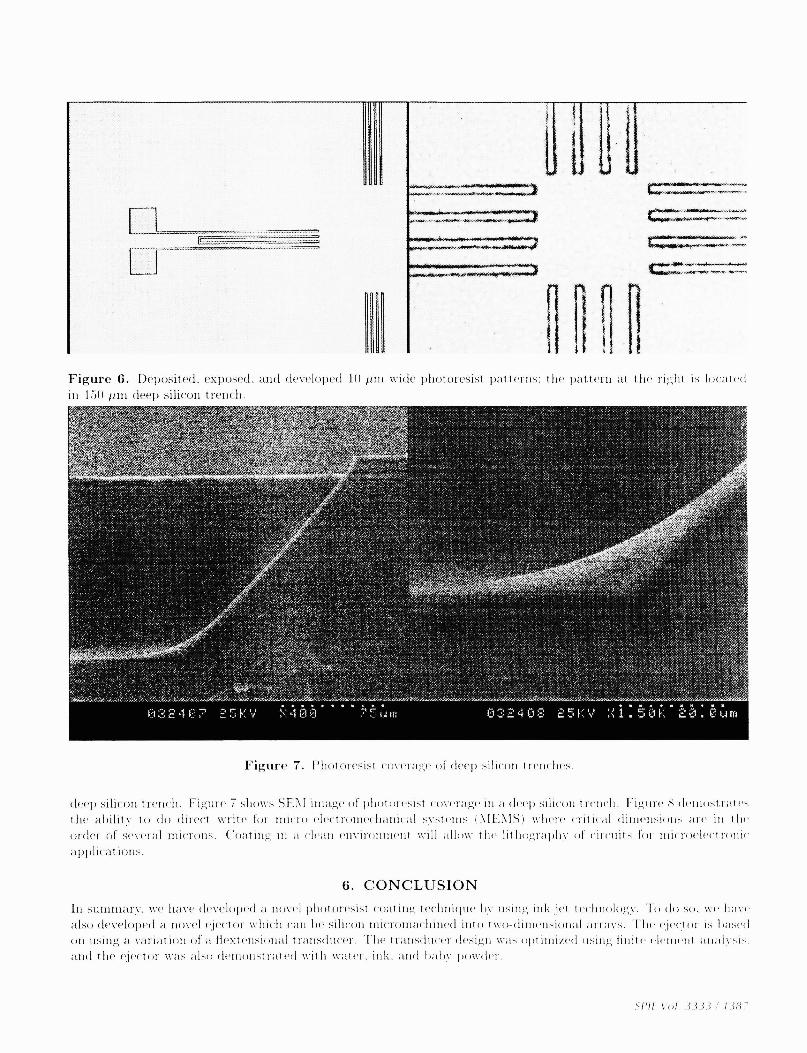
(l1(J) Si11(OIi ti('1i(li. Figure I f1o\vs LT\I ini;tge of fill Ii iit u \(1age iii a (liuji ii1ieoii t reiluli. ligrire rlriiiiIratritin ability to rio dini-ct write for itiuno INtr lIlr(llilili(i(l niin L\1L\lr) vlir unfilial (iinI(niaoie ate Iii tinorder of everai mieron. Coating iii a (lean ellvironhiiruit \viIl Ilio\v tin lii iiogiapliv of (ir(iittH to iiiiuioelertroiiir
1n)ii(.
6. CONCLUSIONIn uiiiiiiirv. \'e lia'i (ieV(1l(f)e(l a novel pliot reiiit I atilig ieiliiiirjiie liv iiitig ink let lerliiiologv. to rio so. wo liavralsO (ieveloj)rrl a novel (jertor \\ill(1l iaii in silicon iiiicroiii;oiiinrd Into tWo-(iI Irulsional arrays. Ha factor is lasadon uisiiig a variation of a Hextetisional transriitcer, Fire iratisdiirer rirsigir v;r opt nuiiii.rd rising tiiiitc rhnani irnilvsis.;uirl tim efector was also dcnioiisirrteri with water. ink, and baby jro'di
IJI oI 3i / JJBT
LI
==-
EHUiU
f1flflrFigure 6. Deposited. exposed and developed 1(1
1 di /1111 (Ieej) siliroii treim(11./1111 vide pliotoir_sist patterns: the jriitterll at (lie right is located
Figure 7. Piii>tonesist veiagr ol deep silicon tnenr'Iirs.

Tahlc 2. SIupli'v \1iioposit punt rosisi p;aInctors°
PhOtISt Viscosity (cSt) Specific Gravity Volatileby Weight (2j
rs1805 5 __10183S1813 20 1.04 73
S1400-21 8 1.02--
7918 1.02
-- -- 73
i 0 0 3 0 0 a
lu iihni m1jIn nhm ihni m
Figure 8. F)r j)—oll—(lelnaIl(l (Iir('(t \\1lt(' with pilot ((r(5!St.
ACKNOWLEDGMENTSThis research was supporter! by hr Defense Advanced flesearcii Proect.s Ageiicv of till' I )epartnleiit of I)efense 011(1
was IIIoIlit()te(1 by tile Air Force other oh Scieiitihc flesearcli tuider (;rant No. F 19(k1ti-9[— 1—h2.
REFERENCES1. —. I3aen. personal coInniulucat 1(111 . Adioiced Process ('oiicepts. BAGENo;loi.colli. 11)97.2. B. Bednar. J. KrdliOek. and .1. Liulioval. Resists in Mu1oliIl(oqli phj itiil 11iio/ioq, ['Isevier ')ci(li(e Publishers
B. \.. A.nisterdaiii, pp. 77—2. i993.
3. 1.. Leviii aiici 13. 1. Kiniri—akuli. 1iiiid (IrojI ('!e(tor nOd iiuethiod. t, Pateiil Applicitiini •\pplicntioii No.
)/.3t) 919 1996.I. (. Perçin. L. Levin. and II. 1. kiiui-\kiib. Piezoeleitriuitllv ot1i;i1(d I raiisdiicer (11(1 (hloplIl (jeltol.
Pioeeed77o.s of I 996 IEEE (1/ IO.S01Il(5 iJ!1i7)05l 010. . 1)13—916. 1996.
G. Perçiii. L. Levii. and 13. 1. khiuiri-\;ikiib. I'iet 'led rnahiv otuiaied droplel ejedl or. iii Heron of 'riiti/Iris truIni(nis 68. pp. 16 1 1997.
6. (. Perçiii 111(1 13. T. I\1iliri-ak1il). Microiiiaihiined 2-1) array pi('voel('dt molly artuiated Iiext('lisioIi;tl I mauisduc-
ers.' iii 19ociedinqs of 11)97 JI'.IE ( T//r1 soi//cs '/1npo.s? mi. 1997.
7. 0. Perçiii ..hdu11aii Atiilar. F. Leveiut Degertekin. nih1 B. I. I\Ii(lrI-\ akiuli. "\1irro1iinrIliIied I so dllll('llsiOlliilarray piezoelectricallv 0(1 ullte(l traiisdiuers. Ill :171/110(1 TVo1.'nis L(tIdi.s 72. ;Id((la('(I L l99,.\..\l..\llnverdiev. N. 13 \khiuuednv arid 1. 1). Slierruiergor. ( 0111(11(1 flexiiriul—s!ienr ((5ii1I;(I,I(i1r- Ii stepwise—
layered plezoceralilic dusk triuisdiicers. iii J'uikludriaiin Ir//u,iimkn (Iliussiaui 23. pp. .9- 6). lt)7.9. M. F. \assergiser. A. N. Viririiihu'uiko. and A. (. i)omosli. ('alriul;mtuoui arid irivestigatioli (If liexuirnl-uiooir j>le/m-
rice nc lush transdUcers ((Ii i/ 1(0551Vd siulisl rate in 1(11' i/lion 011(1 radnal tori. iii oiimct fl////sOs 'boiesto.s 38. Ii-19112.
I 388 . P1L tot 3333

10. H. Okada, M. Kurosawa, S. Ueha, and M. Masuda, "New airborne ultrasonic transducer with high output soundpressure level," in Japan Journal of Applied Physics Part 1 33, pp. 3040-3044, 1994.
11. A. Tula, N. Lamberti, G. Caliano, M. Pappalardo, "A matrix model of the thin piezoceramic ring," in Proceedingsof 19!11j IEEE Ultrasonics Symposium, pp. 921-924, 1994.
12. L. Strom, "The generation of monodisperse aerosols by means of a disintegrated jet of liquid," in Review ofScientific Instruments 40, pp. 778-782, 1969.
13. N. Maehara, S. Ueha, and E. Mori, "Optimum design procedure for multi-pinhole-plate ultrasonic atomizer," inJapanese Journal of Applied Physics Supplement 26-1 26, pp. 215-217, 1987.
14. N. Maehara, S. Ueha, and E. Mori, "Influence of the vibrating system of a multipinhole-plate ultrasonic nebulizeron its performance," in Review of Scientific Instruments 57, pp. 2870-2876, 1986.
15. S. Ueha, N. Maehara, and E. Mori, "Mechanism of ultrasonic atomization using a multipinhole plate," in Journalof Acoustical Society of Japan 6, pp. 21-26, 1985.
16. N. Maehara, K. Hashido, and H. Hirata, "Arrangement for ejecting liquids," European Patent Application,Application No. 823054448.1, Publication No. 0 077 636, 1982.
17. Y. Ivri, "Ultrasonic fluid ejector," International Patent Application, Application No. PCT/US92/05275, Publi-cation No. W093/01404, 1993.
18. I. Tetsuo, "Drop generator for ink jet," Patent Abstracts of Japan, European Patent Office, Application No.JP820185859, Publication No. JP59073963, 1984.
19. A. W. Leissa, Vibration of Plates, Scientific and Technical Information Division, Office of Technology Utilization,NASA, pp. 1-10, 1969.
20. M. K. Kwak, "Vibration of circular membranes in contact with water," in Journal of Sound and Vibration 178,pp. 688-690, 1994.
21. G. Brenn and U. Lackermeier, "Drop formation from a vibrating orifice generator driven by modulated electricalsignals," in Physics of Fluids 9, pp. 3658-3669, 1997.
22. S. C. Tsai, P. Luu, P. Childs, A. Teshome, and C. S. Tsai, "The role of capillary waves in two-fluid atomization,"in Physics of Fluids 9, newblock pp. 2909-2918, 1997.
23. J. Bauer, G. Drescher, and M. hug, "Surface tension, adhesion and wetting of materials for photolithographicprocess," in Journal of Vacuum Science and Technology Part B 14, pp. 2485-2492, 1996.
24. Y. D. Shikhmurzaev, "Spreading of drops on solid surfaces in a quasi-static regime," in Physics of Fluids 9, pp.266-275, 1997.
25. A. L. Yarin and D. A. Weiss, "Impact of drops on solid surfaces: self-similar capillary waves, and splashing as anew type of kinematic discontinuity," in Journal of Fluid Mechanics 283, pp. 141-173, 1995.
26. C. H. R. Mundo, M. Sommerfeld, and C. Tropea, "Droplet-wall collisions: experimental studies ofthe deformationand breakup process," in International Journal of Multiphase Flow 21, pp. 151-173, 1995.
27. 5. H. Davis and D. M. Anderson, "Spreading and evaporation of liquid drops on solids," in ASME AMDSurface-Tension-Driven Flows 170, pp. 1-7, 1993.
28. M. Pasandideh-Fard, Y. M. Qiao, S. Chandra, and J. Mostaghimi, "Capillary effects during droplet impact ona solid surface," in Physics of Fluids 8, pp. 650-659, 1996.
29. Murata Electronics North America, Inc., 2200 Lake Park Drive, Smyrna, GA 30080.30. Motorola, Ceramic Products Division, 4800 Alameda Blvd. N.E., Albuquerque, NM 87113.31. Shipley Company, 455 Forest Street, Marlboro, MA 01752.
SPIE Vol. 3333 / 1389
Copyright © 2022 FDOKUMEN