Flexible, transparent single-walled carbon nanotube transistors with graphene electrodes
Upload
independentCategory
view
0download
0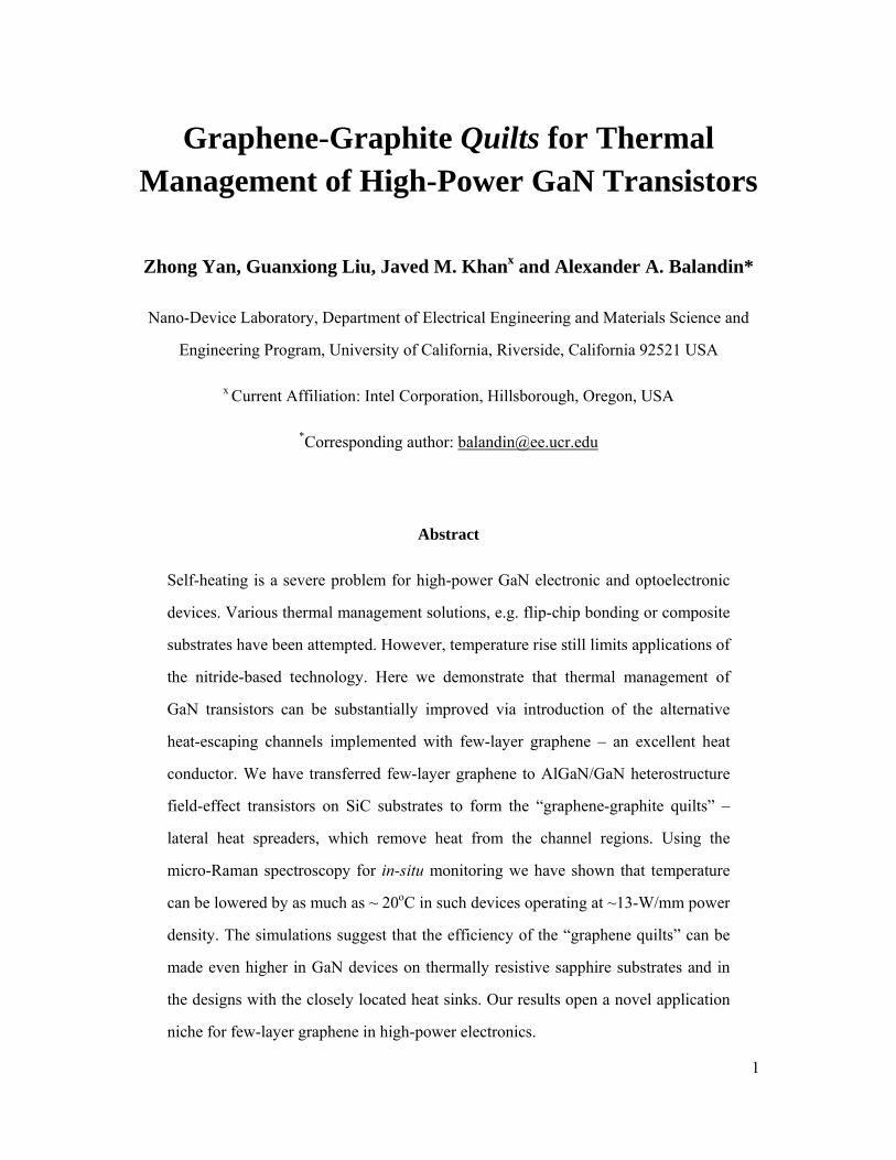
1
Graphene-Graphite Quilts for Thermal Management of High-Power GaN Transistors
Zhong Yan, Guanxiong Liu, Javed M. Khanx and Alexander A. Balandin*
Nano-Device Laboratory, Department of Electrical Engineering and Materials Science and
Engineering Program, University of California, Riverside, California 92521 USA
x Current Affiliation: Intel Corporation, Hillsborough, Oregon, USA
*Corresponding author: [email protected]
Abstract
Self-heating is a severe problem for high-power GaN electronic and optoelectronic
devices. Various thermal management solutions, e.g. flip-chip bonding or composite
substrates have been attempted. However, temperature rise still limits applications of
the nitride-based technology. Here we demonstrate that thermal management of
GaN transistors can be substantially improved via introduction of the alternative
heat-escaping channels implemented with few-layer graphene – an excellent heat
conductor. We have transferred few-layer graphene to AlGaN/GaN heterostructure
field-effect transistors on SiC substrates to form the “graphene-graphite quilts” –
lateral heat spreaders, which remove heat from the channel regions. Using the
micro-Raman spectroscopy for in-situ monitoring we have shown that temperature
can be lowered by as much as ~ 20oC in such devices operating at ~13-W/mm power
density. The simulations suggest that the efficiency of the “graphene quilts” can be
made even higher in GaN devices on thermally resistive sapphire substrates and in
the designs with the closely located heat sinks. Our results open a novel application
niche for few-layer graphene in high-power electronics.
2
Self-heating is a severe problem for the high-power GaN electronic, optoelectronic and
photonic devices [1-3]. Temperature rise and non-uniform distribution of dissipated power in
GaN transistors result in degradation of the drain current, gain and output power, as well as
an increase in the gate-leakage current and poor reliability [1]. Various thermal management
solutions, e.g. flip-chip (FC) bonding [4] or diamond composite substrates [5] have been
attempted. However, the hot spots, which appear owing to the high power densities and
relatively high thermal resistance of the substrates [6-7], still limit applications of the
nitride-based technology [1-3]. For example, AlGaN/GaN HFETs are attractive devices for
high-frequency high-power communications and radar applications [1-2, 8]. Owing to the
large band-gap, saturation velocity of charge carries and breakdown electrical field,
AlGaN/GaN HFETs can operate at extremely high power density of tens of W/mm of the
channel width, which is unattainable with other technologies [9-10]. Unfortunately, at such
power levels, Joule heating starts to degrade performance of GaN devices causing reliability
problems. The mean-time to failure (MTTF) of GaN transistors decreases rapidly with
increasing junction temperature of the devices [1].
A number of methods have been used to improve heat removal from GaN devices.
Conventional sapphire substrates with low thermal conductivity of K~30 W/mK at room
temperature (RT) have been replaced with more expensive SiC substrates with the high
thermal conductivity of K~100 – 350 W/mK at RT. However, even in GaN transistors on SiC
substrate, self-heating can lead to temperature rises, T, above 180oC. The composite
substrates [5] and FC bonding [4] were utilized to improve the heat removal by reducing the
thermal resistance on the scale of the whole wafer. Despite these efforts, the problems of the
hot spots that develop near the downscaled device channels – at the nanometer and
micrometer-scale – still persist. In this communication we demonstrate that thermal
management of AlGaN/GaN heterostructure field-effect transistors (HFET) can be
substantially improved via introduction of the additional heat-escaping channels – top-surface
heat spreaders – made of few-layer graphene (FLG). FLG reveals an order-of-magnitude
higher thermal conductivity, K, than that of GaN, which ranges from 125 to 225 W/mK at RT
[6-7].
3
Here, we propose and examine a conceptually alternative approach for thermal
management of high-power density devices. Instead of trying to further reduce the thermal
resistance, RT, of the substrate, we introduce the lateral heat spreaders on top of the GaN
device structure, which provide additional heat escape channels from the hot spots. Ideally,
the heat spreader should be made from material with the highest K as possible. It was recently
discovered by some of us that graphene has the highest intrinsic thermal conductivity of all
known materials, which increases with the lateral size [11-12]. From the practical
applications point of view, FLG is better because its K is less subject to deterioration due to
extrinsic effects, e.g. defects and disorder at the interfaces [12]. In addition, FLG and thin
graphite films allow for the larger in-plane heat flux through its cross-section while still
preserving graphene’s mechanical flexibility.
Experimental Results
In order to perform the proof-of-concept demonstration, we transferred FLG and graphite
films exfoliated from the highly-oriented pyrolytic graphite (HOPG) to the AlGaN/GaN
devices on SiC substrate. Some of the flakes were naturally attached to thicker graphite
regions. Graphite has high thermal conductivity (K≈2000 W/mK) and can be utilized both for
heat spreaders and heat sinks depending on the thickness, geometry and size [12]. The fast
progress in various chemical methods of large-area FLG growth [13-16], stimulated by strong
interest to graphene, suggests that deposition of FLG and graphite on substrates with
controlled number of the atomic planes, n, will soon become a commercial technology. The
latter will facilitate practical applications of FLG for heat spreading. The graphite heat sinks
can also be replaced with the metallic sinks or vertical thermal vias connected to the bottom
heat sink.
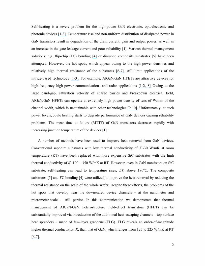
Figure 1a-f illustrates the concept of “graphene-graphite quilts” as the top-surface heat
spreaders and provides their microscopy images. We used AlGaN/GaN HFETs with the
layered structure consisting of 30-nm AlGaN (~20% Al) barrier on 0.5-µm-thick GaN
4
channel layer deposited on insulating 4H-SiC substrate. The source and drain metal contacts
were made of Ti/Al/Ti/Au while the gate electrode was made of Ni/Au. Details of the device
structure and fabrication of typical AlGaN/GaN HFETs can be found in literature [8-10].
Figure 1: “Graphene-graphite quilts” as the top-surface heat spreaders for AlGaN/GaN HFETs. 1a: Optical microscopy of AlGaN/GaN HFETs before fabrication of the heat spreaders. 1b: Schematic of the FLG-graphite heat spreaders attached to the drain contact of the AlGaN/GaN HFET. 1c: SEM image of the heat spreader transferred to the drain contact. The “graphene-graphite quilt” is indicated with the green color while metal contacts are with the yellow color. 1d: Optical microscopy image of the “quilt” overlapping the metal drain contact and GaN surface demonstrating the heat spreader’s flexibility and its close contact with the surface. 1e: SEM image of the heat spreader – metal contact region and GaN surface. 1f: Schematic of the device structure and the “graphene-graphite quilt” used in the simulation for the heat spreader optimization. Dark blue indicates the AlGaN barrier layer. Note that the FLG layer can be extended all the way to the space between the drain and the gate.
The gate length and widths of the devices used in this study were 3.5 μm and 90 μm,
respectively. The large source-drain separation of 12 μm facilitated the heat spreader
fabrication. The direct HOPG exfoliation on GaN/SiC substrate cannot be accomplished
owing to the random nature of the process. For this reason, we applied the PMMA-assisted
method [17] with some modifications, which allowed us an accurate placement of
FLG-graphite “quilts” in pre-determined locations on top of GaN devices. The heat spreaders
5
were attached to the drain contacts of the devices – the closest to the hot spots – according to
reported simulations [18-19]. We carefully avoided short-circuiting GaN devices making sure
that the “graphene quilts” extend from the drains directly to the graphite heat sinks on the
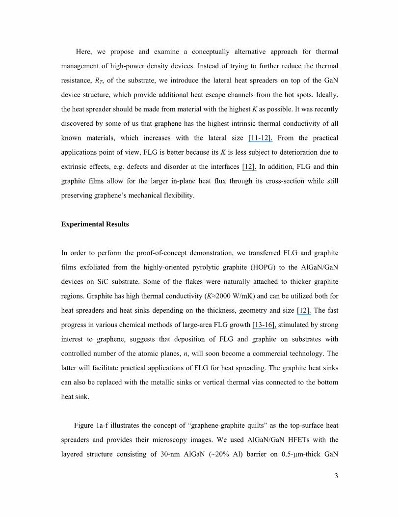
side of the devices. Figure 2 shows the schematic of the process of FLG transfer to GaN
structure. The details are given in the Methods section.
Figure 2: Transfer of FLG films to exact locations on AlGaA/GaN HFET device structure. The first set of steps, indicated by blue arrows, includes spin coating of the photoresist and PMMA, followed by FLG exfoliation on top of PMMA. The second set of steps, indicated by red arrows, consists of dissolving photoresist and attaching graphene to glass slides. The slide is micro-manipulated over AlGaN/GaN HFET to exact location under optical microscope. Dissolution of PMMA leaves FLG film in the desired location. Micro-Raman inspection confirms the number of layers and the quality of FLG after the transfer process.
The AlGaN/GaN HFETs with the heat spreaders and the reference HFETs without the
heat spreaders have been wire-bonded and placed under the Raman microscope (Renishaw
inVia). Raman spectroscopy was utilized both for quality control of FLG and graphite films
after the transfer process and for in-situ monitoring of T in the powered devices. The
non-contact and non-destructive micro-Raman spectroscopy technique has been previously
used for T mapping in AlGaN/GaN devices by measuring the temperature-dependent shifts in
the Raman peak positions [10, 20]. We performed the measurements in the backscattering
6
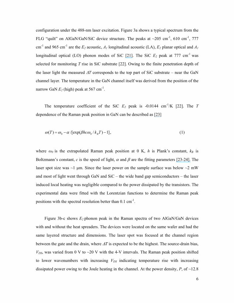
configuration under the 488-nm laser excitation. Figure 3a shows a typical spectrum from the
FLG “quilt” on AlGaN/GaN/SiC device structure. The peaks at ~205 cm-1, 610 cm-1, 777
cm-1 and 965 cm-1 are the E2 acoustic, A1 longitudinal acoustic (LA), E2 planar optical and A1
longitudinal optical (LO) phonon modes of SiC [21]. The SiC E2 peak at 777 cm-1 was
selected for monitoring T rise in SiC substrate [22]. Owing to the finite penetration depth of
the laser light the measured T corresponds to the top part of SiC substrate – near the GaN
channel layer. The temperature in the GaN channel itself was derived from the position of the
narrow GaN E2 (high) peak at 567 cm-1.
The temperature coefficient of the SiC E2 peak is -0.0144 cm-1/K [22]. The T
dependence of the Raman peak position in GaN can be described as [23]
]1)//[exp()( 00 TkhcT B , (1)
where ω0 is the extrapolated Raman peak position at 0 K, h is Plank’s constant, kB is
Boltzmann’s constant, c is the speed of light, and are the fitting parameters [23-24]. The
laser spot size was ~1 μm. Since the laser power on the sample surface was below ~2 mW
and most of light went through GaN and SiC – the wide band gap semiconductors – the laser
induced local heating was negligible compared to the power dissipated by the transistors. The
experimental data were fitted with the Lorentzian functions to determine the Raman peak
positions with the spectral resolution better than 0.1 cm-1.
Figure 3b-c shows E2 phonon peak in the Raman spectra of two AlGaN/GaN devices
with and without the heat spreaders. The devices were located on the same wafer and had the
same layered structure and dimensions. The laser spot was focused at the channel region
between the gate and the drain, where T is expected to be the highest. The source-drain bias,
VDS, was varied from 0 V to ~20 V with the 4-V intervals. The Raman peak position shifted
to lower wavenumbers with increasing VDS indicating temperature rise with increasing
dissipated power owing to the Joule heating in the channel. At the power density, P, of ~12.8
7
W/mm the temperature rise, T, was 92oC for the AlGaN/GaN HFET with the “graphene-
graphite quilt” and T=118oC in the HFETs without the heat spreader. In this specific
example, the same P was achieved in the devices at 20 V and 22 V due to small variations in
the current-voltage characteristics (I-Vs). The corresponding T in the top region of SiC
substrate was 44oC and 30oC in the HFETs without and with the heat spreader, respectively.
Our experimental data indicate that even at the moderate P, the “graphene-graphite quilts”
can help to reduce the hot-spot temperature in AlGaN/GaN HFETs.
Figures 3d and 3e present I-V characteristics of representative AlGaN/GaN HFETs
while Figure 3f gives comparison of I-Vs of the HFETs with and without the heat spreaders.
The tested device was completely pinched off at negative gate bias VG=-4 V. The maximum
source-drain current density of ISD=0.75 A/mm was obtained at a positive gate bias VG=2 V.
The negative-slope regions in I-V curves indicate a degradation of the carrier mobility due to
Joule heating as the dissipated power increases (see Figure 3d). Figure 3e shows I-Vs of the
same device at elevated ambient temperature, TA. The ambient temperature was changed by
placing the device on a hot chuck. The saturation current density, IDS, decreases rapidly with
increasing TA. For a given device IDS follows the equation ADS TI 0014.0487.0 . The
obtained I-V characteristics and their dependence on TA are in agreement with literature
[X-X]. The data illustrate the importance of temperature effects on performance of
AlGaN/GaN HFETs. The insets to Figure 3e shows one of the tested devices and Raman SiC
E2 peak for the low and high VDS in HFET without the heat spreader.
Figure 3f provides direct comparison of I-Vs characteristics before (solid lines) and after
(dashed lines) introduction of the “graphene-graphite quilts”. At VG=2 V, ISD increases from
~0.75 A/mm to ~0.84 A/mm – 12 % improvement – as a result of better heat removal with
the top lateral heat spreaders. At VG=0 V, ISD increased from 0.47 A/mm to 0.51 A/mm,
which is 8 % improvement. At VG=-2V, the current density remains almost the same after
introduction of the heat spreader owing to the low dissipation power density at this negative
8
gate bias. These experiments present a direct evidence of the improvement in the
AlGaN/GaN HFET performance with the top-surface heat spreaders.
Figure 3: Micro-Raman monitoring of the temperature rise in the device structure and I-V characteristics of AlGaN/GaN HFETs. 3a: Raman spectrum of FLG on top of AlGaN/GaN structure on SiC substrate. The luminescence background alters the intensity ratios. To make the small peak easily distinguishable the original spectrum (red) is shown under ×10- magnification (blue). 3b: E2 peak shift in AlGaN/GaN HFET without the heat spreader at the power density P=12.8 W/mm. 3c: Smaller E2 peak shift in AlGaN/GaN HFET with the heat spreader indicating a reduction in the temperature rise at the same power density. 3d: I-V characteristics of a typical tested device showing self-heating effects at the high current density. 3e: Saturation current degradation with increasing ambient temperature. Insets show one of the tested devices and SiC E2 Raman peak used for temperature monitoring inside the GaN substrate. 3f: Comparison of I-Vs of AlGaN/GaN HFETs with and without “graphene- graphite quilts” indicating improvement in I-Vs of HFETs with the heat spreaders.
Simulation Results and Discussion
To rationalize the experimental results and estimate the achievable improvements in thermal
management of AlGaN/GaN HFETs on different substrates we simulated heat propagation in
AlGaN/GaN layered device structures using the finite-element method (see Supplementary
Materials). The thickness of SiC substrate, GaN, AlGaN and SiO2 layers were 0.4 mm, 0.5
9
μm, 30 nm and 10 nm, respectively. Their corresponding RT thermal conductivities were
taken from literature to be 350 W/mK, 160 W/mK, 120 W/mK and 1.4 W/mK [7-8, 25].
Thermal conductivity of FLG was assumed to be 2000 W/mK [12]. Thermal boundary
resistance (TBR) at the GaN-substrate interface plays an important role in self-heating effects
[18-19]. The TBR value RB=1.5×10⁻⁸ m2K/W was chosen to be consistent with the reported
experimental [2, 26] and numerical studies [27]. To make sure that the assumed K values for
the layers are reasonable, we measured the effective thermal conductivity of the whole
AlGaN/GaN/SiC device structure. The measurements were performed using the “laser-flash”
technique (see Supplementary Materials). The affective K for the whole structure was
300±56 W/mK at RT. This value is in line with the data from literature for each individual
layer taking into account the unavoidable contributions of TBR at several interfaces [18].
In the model, we defined the heat source at the AlGaN-GaN interface and selected the
boundary conditions at the substrate bottom to be RT. To validate the developed model with
the experimental data we simulated T distribution in AlGaN/GaN HFETs without the heat
spreader at P=12.8 W/mm. The device structure parameters corresponded to the actual tested
HFET. The simulation gave T=119oC for GaN channel (see Figure 4a), which is in excellent
agreement with the measured T=119oC. The simulated T in the upper region of SiC is also
in line with the experimental data. The procedure was repeated for the AlGaN/GaN HFETs
with the heat spreader of the geometry similar to the experimental structure. The simulated
T=102oC in GaN channel is in agreement with the measurement within the ~10%
uncertainty (Figure 4b).
Using the validated model we determined T profiles in AlGaN/GaN HFETs with
different heat spreader designs (Figure 4c-d). We used FLG with the number of atomic planes
n=10 and the heat sink located at the distance, D, of 10 m and 1 m. Addition of the
“graphene-graphite quilt” reduces temperature of the hot spot. The device structures with the
closely located heat sinks offer stronger T reduction (Figure 4d). In the practical designs, the
nearby heat sinks attached to the top-surface heat spreaders can be implemented with the
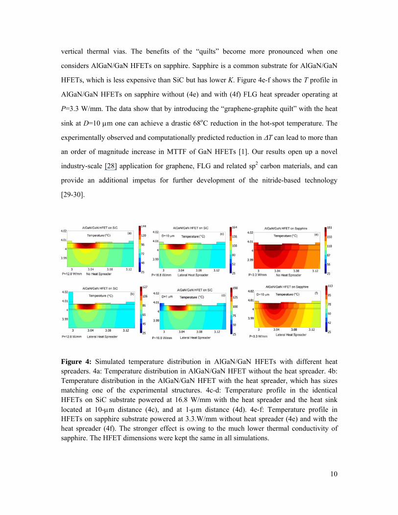
10
vertical thermal vias. The benefits of the “quilts” become more pronounced when one
considers AlGaN/GaN HFETs on sapphire. Sapphire is a common substrate for AlGaN/GaN
HFETs, which is less expensive than SiC but has lower K. Figure 4e-f shows the T profile in
AlGaN/GaN HFETs on sapphire without (4e) and with (4f) FLG heat spreader operating at
P=3.3 W/mm. The data show that by introducing the “graphene-graphite quilt” with the heat
sink at D=10 m one can achieve a drastic 68oC reduction in the hot-spot temperature. The
experimentally observed and computationally predicted reduction in T can lead to more than
an order of magnitude increase in MTTF of GaN HFETs [1]. Our results open up a novel
industry-scale [28] application for graphene, FLG and related sp2 carbon materials, and can
provide an additional impetus for further development of the nitride-based technology
[29-30].
Figure 4: Simulated temperature distribution in AlGaN/GaN HFETs with different heat spreaders. 4a: Temperature distribution in AlGaN/GaN HFET without the heat spreader. 4b: Temperature distribution in the AlGaN/GaN HFET with the heat spreader, which has sizes matching one of the experimental structures. 4c-d: Temperature profile in the identical HFETs on SiC substrate powered at 16.8 W/mm with the heat spreader and the heat sink located at 10-m distance (4c), and at 1-m distance (4d). 4e-f: Temperature profile in HFETs on sapphire substrate powered at 3.3.W/mm without heat spreader (4e) and with the heat spreader (4f). The stronger effect is owing to the much lower thermal conductivity of sapphire. The HFET dimensions were kept the same in all simulations.
11
METHODS
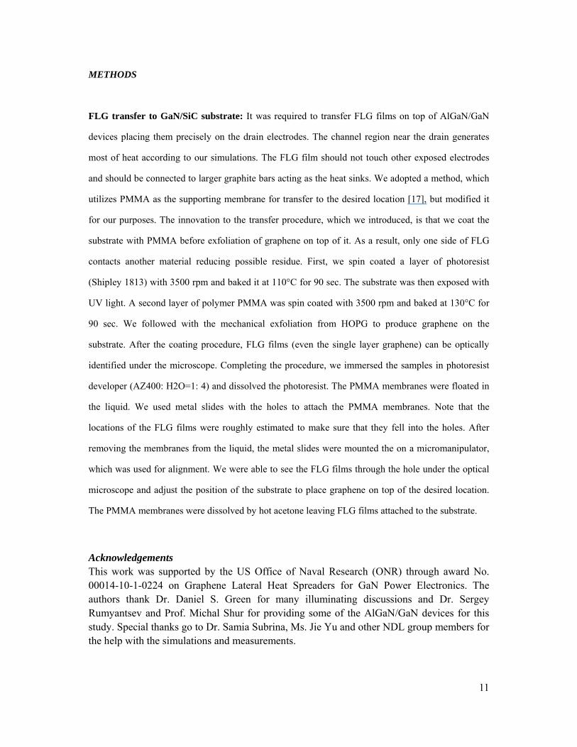
FLG transfer to GaN/SiC substrate: It was required to transfer FLG films on top of AlGaN/GaN
devices placing them precisely on the drain electrodes. The channel region near the drain generates
most of heat according to our simulations. The FLG film should not touch other exposed electrodes
and should be connected to larger graphite bars acting as the heat sinks. We adopted a method, which
utilizes PMMA as the supporting membrane for transfer to the desired location [17], but modified it
for our purposes. The innovation to the transfer procedure, which we introduced, is that we coat the
substrate with PMMA before exfoliation of graphene on top of it. As a result, only one side of FLG
contacts another material reducing possible residue. First, we spin coated a layer of photoresist
(Shipley 1813) with 3500 rpm and baked it at 110°C for 90 sec. The substrate was then exposed with
UV light. A second layer of polymer PMMA was spin coated with 3500 rpm and baked at 130°C for
90 sec. We followed with the mechanical exfoliation from HOPG to produce graphene on the
substrate. After the coating procedure, FLG films (even the single layer graphene) can be optically
identified under the microscope. Completing the procedure, we immersed the samples in photoresist
developer (AZ400: H2O=1: 4) and dissolved the photoresist. The PMMA membranes were floated in
the liquid. We used metal slides with the holes to attach the PMMA membranes. Note that the
locations of the FLG films were roughly estimated to make sure that they fell into the holes. After
removing the membranes from the liquid, the metal slides were mounted the on a micromanipulator,
which was used for alignment. We were able to see the FLG films through the hole under the optical
microscope and adjust the position of the substrate to place graphene on top of the desired location.
The PMMA membranes were dissolved by hot acetone leaving FLG films attached to the substrate.
Acknowledgements This work was supported by the US Office of Naval Research (ONR) through award No. 00014-10-1-0224 on Graphene Lateral Heat Spreaders for GaN Power Electronics. The authors thank Dr. Daniel S. Green for many illuminating discussions and Dr. Sergey Rumyantsev and Prof. Michal Shur for providing some of the AlGaN/GaN devices for this study. Special thanks go to Dr. Samia Subrina, Ms. Jie Yu and other NDL group members for the help with the simulations and measurements.
12
References
[1] Trew, R. J., Green, D. S. & Shealy, J. B. AlGaN/GaN HFET reliability. IEEE Microw.
Mag. 10, 116 (2009).
[2] Kuzmik, J. et al. Self-heating phenomena in high-power III-N transistors and new thermal
characterization methods developed within EU project TARGET. Int. J. Microwave and
Wireless Tech. 1(2), 153 (2009).
[3] Green, D. S. et al. GaN HEMT thermal behavior and implications for reliability testing
and analysis. Phys. Stat. Sol. (c) 5, 2026 (2008).
[4] Sun, J. et al. Thermal management of AlGaN–GaN HFETs on sapphire using flip-chip
bonding with epoxy underfill. IEEE Elec. Dev. Lett. 24, 375 (2003).
[5] Kidalov, S.V. & Shakhov, F. M. Thermal conductivity of diamond composites. Materials
2, 2467 (2009).
[6] Zou, J., Kotchetkov, D., Balandin, A. A., Florescu, D. I. & Pollak, F. H. Thermal
conductivity of GaN films: effects of impurities and dislocations. J. Appl. Phys. 92, 2534
(2002).
[7] Liu, W. L. & Balandin, A. A. Thermal conduction in AlGaN alloys and thin films. J.
Appl. Phys. 97, 073710 (2005).
[8] Balandin, A. A. et al. Low flicker-noise GaN/A1GaN heterostructure field-effect
transistors for microwave communications. IEEE Trans. Microwave Theory and Techniq.,
47, 1413 (1999).
[9] Rajan, S. et al. Power performance of AlGaN–GaN HEMTs grown on SiC by
plasma-assisted MBE. IEEE Elec. Dev. Lett., 25, 247 (2004).
[10] Kuball, M. et al., Measurement of temperature in active high-power AlGaN/GaN HFETs
using Raman spectroscopy. IEEE Elec. Dev. Lett. 23, 7 (2002).
[11] Balandin, A. A. et al. Superior thermal conductivity of single-layer grapheme. Nano
Lett., 8, 902 (2008).
[12] Balandin, A. A. Thermal properties of graphene and nanostructured carbon materials.
Nature Mat., 10, 569 (2011).
[13] Eda, G., Fanchini, G. & Chhowalla, M. Large-area ultrathin films of reduced graphene
oxide as a transparent and flexible electronic material. Nature Nanotech. 3, 270–274 (2008).
13
[14] Park, S. & Ruoff, R. S. Chemical methods for the production of graphenes. Nature
Nanotech. 4, 217–224 (2009).
[15] Kim, K. S. et al. Large-scale pattern growth of graphene films for stretchable transparent
electrodes. Nature 457, 706–710 (2009).
[16] Obraztsov, A. N. Chemical vapour deposition making graphene on a large scale. Nature
Nanotech. 4, 212 (2009).
[17] Dean, C. R. et al. Boron nitride substrates for high-quality graphene electronics. Nature
Nanotech. 5, 722–726 (2010).
[18] Turin, V. O. & Balandin, A. A. Performance degradation of GaN field-effect transistors
due to thermal boundary resistance at GaN/substrate interface. Electron. Lett. 40, 81 (2004).
[19] Turin, V. O. & Balandin, A. A. Electro-thermal simulations of the self-heating effects in
GaN-based field-effect transistors. J. Appl. Phys. 100, 054501 (2006)
[20] Kuball, M. et al. Measurement of temperature distribution in multifinger AlGaN/GaN
heterostructure field-effect transistors using micro-Raman spectroscopy. Appl. Phys. Lett. 82,
124 (2003).
[21] Burton, J. C., Sun, L., Long, F. H., Feng, Z. C. & Ferguson, I. T. First- and second-order
Raman scattering from semi-insulating 4H-SiC. Phys, Rev. B 59, 7282 (1999).
[22] Bauer, M., Gigler, A. M., Huber, A. J., Hillenbrand, R. & Stark, R. W.
Temperature-depending Raman line-shift of silicon carbide. J. Raman Spec., 40, 1867 (2009).
[23] Liu, M. S. et al. Temperature dependence of Raman scattering in single crystal GaN
films. Appl. Phys. Lett. 74, 3125 (1999).
[24] Sarua, A. et al. Integrated micro-Raman/infrared thermography probe for monitoring of
self-heating in AlGaN/GaN transistor structures. IEEE Trans. Electron Dev. 53, 2438 (2006)
[25] Sheppard. S. T. et al. High-power microwave GaN/AlGaN HEMT’s on semi-insulating
silicon carbide substrates. IEEE Elec. Dev. Lett. 20, 161 (1999).
[26] Sarua, A. et al., Thermal boundary resistance between GaN and substrate in AlGaN/GaN
electronic devices. IEEE Trans. Electron Dev. 54, 3152 (2007)
[27] Filippov, K. & Balandin, A. A. The effect of the thermal boundary resistance on
self-heating of AlGaN/GaN HFETs. MRS Internet J. Nitride Semiconductor Research
[Online], 8, article 4 (2003); available at http://nsr.mij.mrs.org/8/4/
[28] Segal, M. Selling graphene by the ton. Nature Nanotech. 4, 612 - 614 (2009).
Copyright © 2022 FDOKUMEN