
English Proceedings
145
College of Instrumentation & Electrical Engineering, Jilin University Academic Practice “Six in One” Training Project English Proceedings 2013 (Second Half)
-
Upload
khangminh22 -
Category
Documents
-
view
2 -
download
0
Transcript of English Proceedings

College of Instrumentation & Electrical Engineering, Jilin University
Academic Practice “Six in One” Training Project
English Proceedings
2013 (Second Half)


I
CONTENTS
Microcontroller-based mobile wireless charger design .........................................Ding Xiaoxu; Guo Baifu; Like 1
Pedestrian Dead Reckoning Device Design Based on STM32......................................................................................
......................................................................................................... Luo Yin; Lu Hongzhou; Zhao Yu; Wang Jun 6
Transit Passenger Flow Statistics System design................................................ Xueyan hu; Lu bai; Xingzhi han 11
Design and Implementation of the full range of sub-control intelligent lighting system ..............................................
.............................................................................................................................. Li Na; Zhang Tao; Ye Jiansong 15
Research on wireless synchronization device in superficial seismic exploration..........................................................
......................................................................................... Zhang Lin-hang; Pei Li-ran; Sun Zi-chao; Wang Cong 19
The Research of Sphere Lifting Height Automatic Control System Based on Air Pressure Control ............................
.................................................................................................... Qian Chenghui; Shi Zhaomin; Kang Lili; Li Qi 25
The design of lowcost Vibroseis based on FPGA.........................Qian Chenghui1; Shi Zhaomin; Li qi; Xu qian 30
Design of Gravitational Acceleration Measuring Device Based on Balance Method ...................................................
..........................................................................................................................Qian Chenghui; Chen Changsong 36
A 3D scanning and laser ranging device based on Triangulation ..................................................................................
...............................................................................CHEN Hao; HAN Xing-Zhi; TANG Xiang-Mei; JIANG Tao 42
The Design and Implementation about attendance system used in campus classroom based on RFID technology......
......................................................................................................................Li Jiaoyang; Wu Ziyu; Piao Guanyu 48
Intelligent Multifunctional lamp.............................................................Zhang Zhuo; Chen jie-yuan; Zhang Wei 54
XYZ three-axis stepper motor control system......................................................... NieYang; LiTengFei; LiuHui 58
The dormitory intelligent security alarm system based on GSM wireless communication...........................................
.......................................................................................................................... JiaoLei; ZhaoYue; WangZhengyu 62
A post-disaster Detection Rescue Robot System Design...............................................................................................
................................................................................................. HU Rui-fan; WANG Hong-chao; PENG Yi-shuai 66
Development of early detection instrument for apnea syndrome ................. Xu Li-xia; Wang Gang; Lian Shi-bo 71
Design of nRF905-based Wireless Greenhouse for Environmental Parameters Detection and Transmission System .
.....................................................................................................................YangShuXin; LiuYang; LengShuZhe 77
Wireless multi-point temperature and humidity detection system design based on nRF24L01 ....................................
...................................................................................................................... Wu Jindi; Song Qihan; Zhao Xiaoyi 81
The teaching auxiliary system based on the light cube..................................................................................................
..........................................................................................................Xin Yi; Zhu Zhanshan; Chen Xu; Jiang Jian 85
Intelligent alarm system based on MMS ....................................................Zhang Yixuan; Zhou Xianze; Liu Yan 88
The calculation of mutual inductance of two polygons with multiturn coils at arbitrarily position ..............................
...........................................................................................................................................LiuYang; HeShengmin 92
Design and Realization of a Secondary Reclosing Microcomputer Device Remotely and Interactively Controlled

II
by PC ......................................................................................................................Han Si-yu; Wang Yu; Ma Jing 97
The Design and Implementation of Electromagnetic Radiation Detector .....................................................................
...............................................................................................................Wang Di; Ren Tian-ming; Jiang Ming-jie 105
The manufacture and simulation for electromagnetical damping of fiber detector .......................................................
....................................................................................................................... Jiang Ransong; Zhou Rui; Xue Bixi 109
Intelligent House Leakage Detection and Alarm System ..............................................................................................
.................................................................................................Li Suyi; Wang Duoqiang; Bai Yang; Zhang Weijie 121
Office computer displayer of electromagnetic radiation measure and alarm system.....................................................
....................................................................................................... Yuan Guiyang; Shen Chunyang; Liu Gucheng 127
The Multi-frequency Signal Generating Technology for the Shallow Surface Detection .............................................
....................................................................................Liu Chang-sheng; Kang Pan; Xia Zheng-yang; Zheng Wei 131
Fuzzy control based on ultrasonic ranging parking system model design.....................................................................
............................................................................QIAN Cheng-hui; FU yu-jing; MIAO Hong-song; KANG-ning 137

Ding Xiaoxu etc.: Microcontroller-based mobile wireless charger design
1
Microcontroller-based mobile wireless charger design
Ding Xiaoxu; Guo Baifu; Like
(Jilin University of Instrument Science and Electrical Engineering, Changchun 130012) Abstract—In order to adapt to the wireless charging of implantable medical devices, sensors, municipal transportation and
other aspects of the application, Change the current electronic charging interface incompatibilities. The design uses a
low-power microcontroller STC12C5A60S2 energy transfer charger as a wireless monitoring and control core,based on the
principle of electromagnetic induction, through energy coupling coil, to achieve energy transfer, the current control, voltage
control, achieve transmission distance 5cm, the voltage reaches 5V, 0.5A current steady power supply, after the prompt is
given full power and full automatically stop charging。Charging voltage and charging current display with low power
LCD1602.System has a wireless charging, energy transfer effect is good, low cost, no wiring, easy to carry and other
advantages, has a broad application prospects.
Keywords—STC12C5A60S2 MCU intelligent wireless charging
FOREWORD
PHONE needs the corresponding charger, most chargers can not be universal and compatible portable wired charger and charge the user is not easy. So a no charger charging technology to be developed. Nokia 920 handset with a wireless charging technology, using electromagnetic induction principle, sending and receiving end have a coil, transmitter coil is connected wired power generating electromagnetic signals, Receiver coil induction sending electromagnetic signals to generate current to the battery. But Nokia 920 wireless charging, you need to put the corresponding wireless charging plate, once more than 2 cm can not be charged, and the production process is complicated, expensive, visible increase the transmission distance is a wireless charging technology should pay attention to the issue. This design uses the same principle of electromagnetic induction to generate energy through the coil coupling, hardware circuits are transmitting and receiving ends of two parts, transmitter using NE555 with the RC oscillation circuit constituted, as a power amplifier using FET devices; Receive comprised BUCK chopper circuit voltage type step-down DC/DC conversion circuit realized steady flow. Transmission
distance can reach 5-10cm, voltage 5V, 0.5A current stable charging. Has simple, wireless transmission distance is long, low-cost advantage. In the design of single chip microcomputer and LCD power consumption is more, lead to the problem of lower charging current, so use low-power chips and liquid crystal display, the charging current can be improved.
1 THE HARDWARE SYSTEM DESIGN
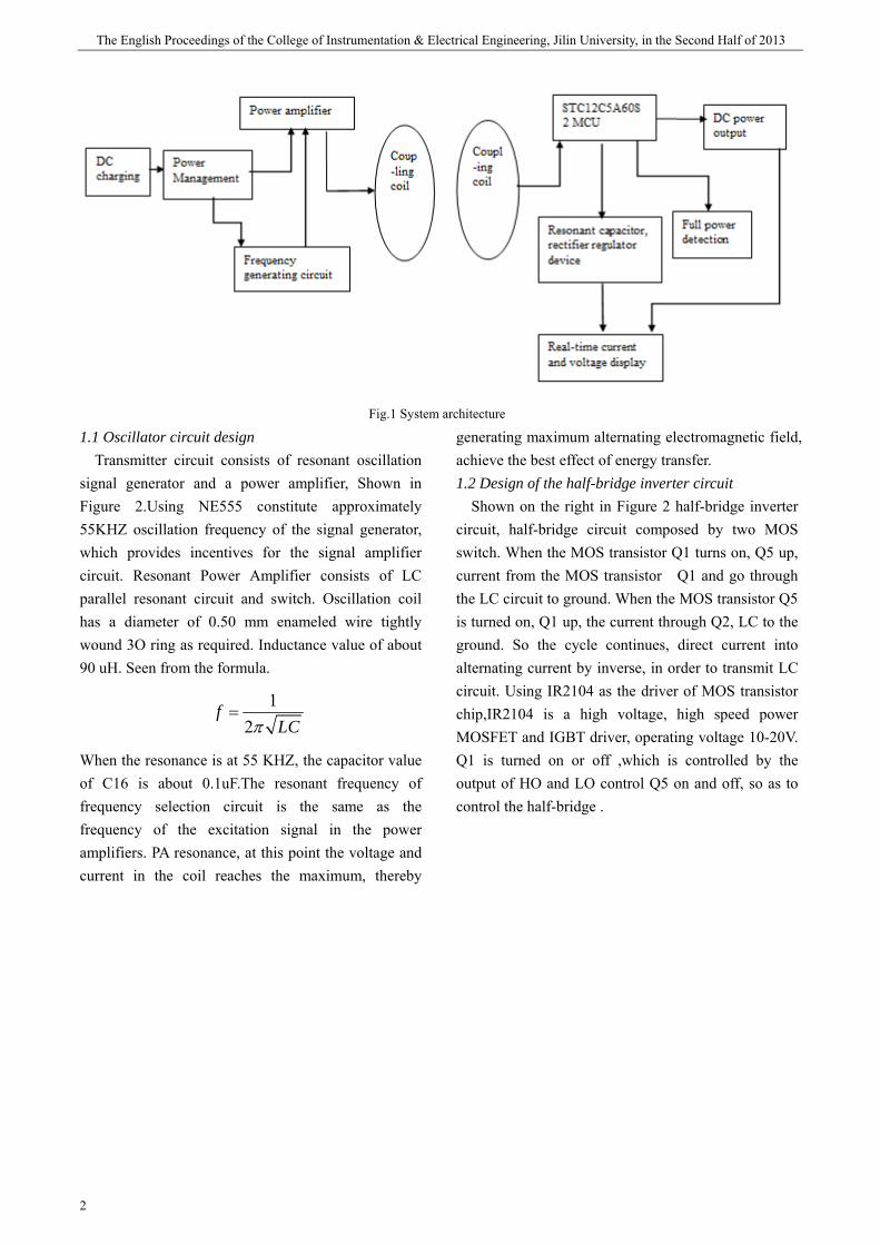
The wireless charging system design using electromagnetic induction principle, the use of coil coupling to transfer energy. Due to the wireless transmission of power voltage with energy sending unit and receiving unit coupling coil spacing D may change in the test, lead to different charging voltage change of distance, design considerations for safety, so charging ways on the choice of constant voltage charging scheme. On the device select select has a variety of power saving mode, power consumption province in particular, Strong anti-interference force of MSP430 ultra-low power MCU series MSP430F2274 as monitoring of wireless transmission can charger control core chip, voltage and charging time display with low power consumption LCD1602 LCD screen, to improve the utilization efficiency of the energy of the charging circuit.
期 The English Proceedings of the College of Instrumentation & Electrical Engineering, Jilin University, in the Second Half of 2013
2
Fig.1 System architecture
1.1 Oscillator circuit design Transmitter circuit consists of resonant oscillation
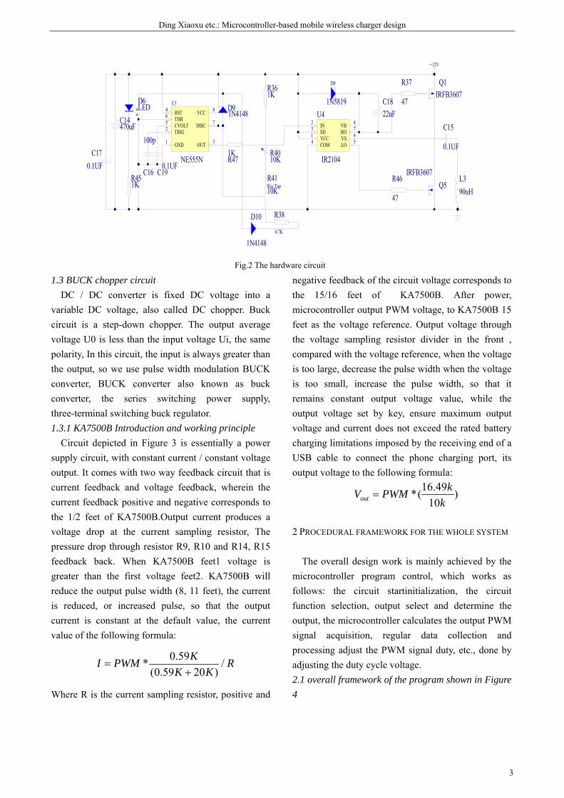
signal generator and a power amplifier, Shown in Figure 2.Using NE555 constitute approximately 55KHZ oscillation frequency of the signal generator, which provides incentives for the signal amplifier circuit. Resonant Power Amplifier consists of LC parallel resonant circuit and switch. Oscillation coil has a diameter of 0.50 mm enameled wire tightly wound 3O ring as required. Inductance value of about 90 uH. Seen from the formula.
12
fLCπ
=
When the resonance is at 55 KHZ, the capacitor value of C16 is about 0.1uF.The resonant frequency of frequency selection circuit is the same as the frequency of the excitation signal in the power amplifiers. PA resonance, at this point the voltage and current in the coil reaches the maximum, thereby
generating maximum alternating electromagnetic field, achieve the best effect of energy transfer. 1.2 Design of the half-bridge inverter circuit
Shown on the right in Figure 2 half-bridge inverter circuit, half-bridge circuit composed by two MOS switch. When the MOS transistor Q1 turns on, Q5 up, current from the MOS transistor Q1 and go through the LC circuit to ground. When the MOS transistor Q5 is turned on, Q1 up, the current through Q2, LC to the ground. So the cycle continues, direct current into alternating current by inverse, in order to transmit LC circuit. Using IR2104 as the driver of MOS transistor chip,IR2104 is a high voltage, high speed power MOSFET and IGBT driver, operating voltage 10-20V. Q1 is turned on or off ,which is controlled by the output of HO and LO control Q5 on and off, so as to control the half-bridge .
Ding Xiaoxu etc.: Microcontroller-based mobile wireless charger design
3
TRIG2
OUT 3
RST4
CVOLT5 THR6
DISC 7
VCC 8
GND1
U3
NE555N
+12V
C190.1UF
C16
100p
R361K
R471K
R38
4.7K
Q5IRFB3607
Q1IRFB3607
R37
47
R46
47
C15
0.1UF
90uHL3
C14470uF
R451K
D6LED
R4010K
VCC1
COM4
VB 8
HO 7
VS 6
LO 5
IN2
SD3
U4
IR2104
D8
1N5819 C1822uF
C170.1UF
10KR41Res Tap
D91N4148
D10
1N4148
Fig.2 The hardware circuit
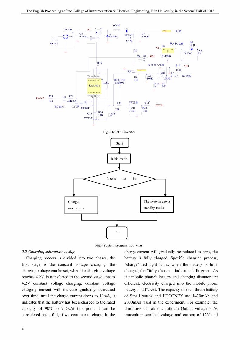
1.3 BUCK chopper circuit DC / DC converter is fixed DC voltage into a
variable DC voltage, also called DC chopper. Buck circuit is a step-down chopper. The output average voltage U0 is less than the input voltage Ui, the same polarity, In this circuit, the input is always greater than the output, so we use pulse width modulation BUCK converter, BUCK converter also known as buck converter, the series switching power supply, three-terminal switching buck regulator. 1.3.1 KA7500B Introduction and working principle
Circuit depicted in Figure 3 is essentially a power supply circuit, with constant current / constant voltage output. It comes with two way feedback circuit that is current feedback and voltage feedback, wherein the current feedback positive and negative corresponds to the 1/2 feet of KA7500B.Output current produces a voltage drop at the current sampling resistor, The pressure drop through resistor R9, R10 and R14, R15 feedback back. When KA7500B feet1 voltage is greater than the first voltage feet2. KA7500B will reduce the output pulse width (8, 11 feet), the current is reduced, or increased pulse, so that the output current is constant at the default value, the current value of the following formula:
0.59* /(0.59 20 )
KI PWM RK K
=+
Where R is the current sampling resistor, positive and
negative feedback of the circuit voltage corresponds to the 15/16 feet of KA7500B. After power, microcontroller output PWM voltage, to KA7500B 15 feet as the voltage reference. Output voltage through the voltage sampling resistor divider in the front , compared with the voltage reference, when the voltage is too large, decrease the pulse width when the voltage is too small, increase the pulse width, so that it remains constant output voltage value, while the output voltage set by key, ensure maximum output voltage and current does not exceed the rated battery charging limitations imposed by the receiving end of a USB cable to connect the phone charging port, its output voltage to the following formula:
16.49*( )10out
kV PWMk
=
2 PROCEDURAL FRAMEWORK FOR THE WHOLE SYSTEM
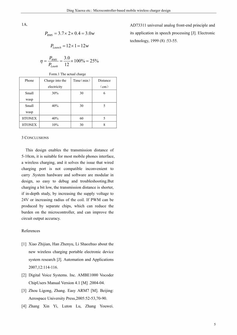
The overall design work is mainly achieved by the microcontroller program control, which works as follows: the circuit startinitialization, the circuit function selection, output select and determine the output, the microcontroller calculates the output PWM signal acquisition, regular data collection and processing adjust the PWM signal duty, etc., done by adjusting the duty cycle voltage. 2.1 overall framework of the program shown in Figure 4
期 The English Proceedings of the College of Instrumentation & Electrical Engineering, Jilin University, in the Second Half of 2013
4
AR1
LM358R201K
AD1
C50.1UF
AD0
1(+
)1
2(-)
1
3FB
4D
TC
5C
T
6R
T
7G
ND
8C
110
E2
9E1
C2
251
12V
CC
13O
C14
RO15
(-)2
16(+
)2
RP1
KA7500B
T1 PNP
R15100
R3
510
D4
IN5819
L1100uH
C3470uF
C2470uF
USB+
USB-
R26.49k
R1810K
R29
1K C9
0.1UF
C10
0.01UF
C13
0.01UF
R3410K
R32300
C113.3UF
PWM1
PWM2
R22590
R23590
R30
20k
C8
0.1UF
100KR21
R16
100k
R24100kR26
1K
+5V
D2
SR260
R3320K
R25470
差分放大电路
滤波RC
滤波RC
滤波RC
R4 0.05
C4
0.1UF
R510k
Vin1
GN
D2
Vout 3U1
LM2940
C1470uF
+5
D1LED
R11K
R28
10KR31
1K
D3
SR260
90uH
L2
USB
单片机电源
N2
N2
Fig.3 DC/DC inverter
Fig.4 System program flow chart
2.2 Charging subroutine design Charging process is divided into two phases, the
first stage is the constant voltage charging, the charging voltage can be set, when the charging voltage reaches 4.2V, is transferred to the second stage, that is 4.2V constant voltage charging, constant voltage charging current will increase gradually decreased over time, until the charge current drops to 10mA, it indicates that the battery has been charged to the rated capacity of 90% to 95%.At this point it can be considered basic full, if we continue to charge it, the
charge current will gradually be reduced to zero, the battery is fully charged. Specific charging process, "charge" red light is lit; when the battery is fully charged, the "fully charged" indicator is lit green. As the mobile phone's battery and charging distance are different, electricity charged into the mobile phone battery is different. The capacity of the lithium battery of Small wasps and HTCONEX are 1420mAh and 2000mAh used in the experiment. For example, the third row of Table I: Lithium Output voltage 3.7v, transmitter terminal voltage and current of 12V and
Start
Initializatio
Needs to be
Charge
monitoring
The system enters
standby mode
End
Ding Xiaoxu etc.: Microcontroller-based mobile wireless charger design
5
1A.
wPRMS 0.34.027.3 =××=
wPLaunch 12112 =×=
%25%10012
0.3=×==
Launh
RMS
PPη
Form.1 The actual charge
Phone Charge into the
electricity
Time(min) Distance
(cm)
Small
wasp
30% 30 6
Small
wasp
40% 30 5
HTONEX 40% 60 5
HTONEX 10% 30 8
3 CONCLUSIONS
This design enables the transmission distance of 5-10cm, it is suitable for most mobile phones interface, a wireless charging, and it solves the issue that wired charging port is not compatible inconvenient to carry .System hardware and software are modular in design, so easy to debug and troubleshooting.But charging a bit low, the transmission distance is shorter, if in-depth study, by increasing the supply voltage to 24V or increasing radius of the coil. If PWM can be produced by separate chips, which can reduce the burden on the microcontroller, and can improve the circuit output accuracy.
References
[1] Xiao Zhijian, Han Zhenyu, Li Shaozhuo about the
new wireless charging portable electronic device
system research [J]. Automation and Applications
2007,12:114-116.
[2] Digital Voice Systems. Inc. AMBE1000 Vocoder
ChipUsers Manual Version 4.1 [M] .2004-04.
[3] Zhou Ligong, Zhang. Easy ARM7 [M]. Beijing:
Aerospace University Press,2005:52-53,70-90.
[4] Zhang Xin Yi, Luton Lu, Zhang Youwei.
AD73311 universal analog front-end principle and
its application in speech processing [J]. Electronic
technology, 1999 (8) :53-55.

期 The English Proceedings of the College of Instrumentation & Electrical Engineering, Jilin University, in the Second Half of 2013
6
Pedestrian Dead Reckoning Device Design Based on STM32
Luo Yin,Lu Hongzhou,Zhao Yu,Wang Jun
College of Instrumentation and Electrical Engineering,JiLin University,Changchun 130012, China Abstract—We put forward a new design of pedestrian dead reckoning device based on the portability and practicality.The
device uses LSM303DLHC integrated with a three-dimensional accelerometer and an electronic compass,and MPU3050
integrated with a gyroscope to collect the real-time movement information of pedestrian.The Cortex-M3 core
STM32F103RBT6 in the device collects data produced by the sensors,performs pedestrian dead reckoning and displays the
dead-reckoning information of pedestrian on a TFTLCD.Experiments prove that the device has the high precision of
dead-reckoning and satisfies the requirement of practical application.
Key words—STM32F103RBT6;multi-sensor;heading;step count;track display
INTRODUCTION
IN the wild woodlands, rocky areas or the urban region located with skyscrapers,the positioning accuracy of global satellite positioning navigation system(GPRS) will descend because of the signal block,it even can’t finish positioning in some circumstances.Therefore in recent years,self-contained positioning scheme based on movement characteristics for pedestrians has become a research hot spot.Most of the adopted solutions use wearable multi-sensor to complete pedestrian dead reckoning(PDR),such as Lei Fang[1] extracted motion information by the sensors worn on the pedestrian waist and transmitted the information to the computer to complete pedestrian dead reckoning.Lauro Ojeda[2] set the gyroscope and three-dimensional accelerometer on the foot to extract information then transmitted it to a computer and use Matlab software for 3D image processing.SUN Zuolei[3] used the particle filter and probabilistic neural network to identify and filter the pedestrian motion information and improved the accuracy of pedestrian dead reckoning.However, the information of PDR of these designs is produced by specialized
software on the computer,it is not very useful,while in the outdoor, the portability of the computer is not high, so the development of a portable, practical pedestrian dead reckoning device is very necessary.For the above design shortcomings combined with the characteristics of pedestrians dead reckoning,we design a portable and practical pedestrian dead reckoning device.It uses three-dimensional accelerometer and electronic compass integrated chip LSM303DLHC and gyroscope integrated chip MPU3050, multiple sensors ensure the accuracy of collected information of pedestrian movement,and ARM Cortex-M3 micro-controller core STM32F103RBT6 as a data processing unit.The real-time processing pedestrian dead reckoning information is displayed on a TFTLCD, which has high data processing accuracy and also meet the needs of portability and practicality.
1 SYSTEM COMPOSITION AND WORKING PRINCIPLE
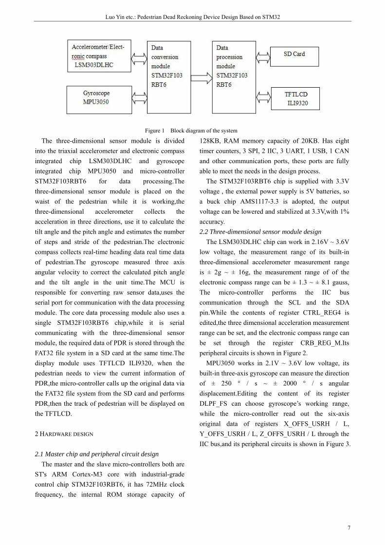
The pedestrian dead reckoning device contains a heading sensor module, a data processing module and a display module, the specific composition diagram is shown in Figure 1.
Luo Yin etc.: Pedestrian Dead Reckoning Device Design Based on STM32
7
Figure 1 Block diagram of the system
The three-dimensional sensor module is divided into the triaxial accelerometer and electronic compass integrated chip LSM303DLHC and gyroscope integrated chip MPU3050 and micro-controller STM32F103RBT6 for data processing.The three-dimensional sensor module is placed on the waist of the pedestrian while it is working,the three-dimensional accelerometer collects the acceleration in three directions, use it to calculate the tilt angle and the pitch angle and estimates the number of steps and stride of the pedestrian.The electronic compass collects real-time heading data real time data of pedestrian.The gyroscope measured three axis angular velocity to correct the calculated pitch angle and the tilt angle in the unit time.The MCU is responsible for converting raw sensor data,uses the serial port for communication with the data processing module. The core data processing module also uses a single STM32F103RBT6 chip,while it is serial communicating with the three-dimensional sensor module, the required data of PDR is stored through the FAT32 file system in a SD card at the same time.The display module uses TFTLCD ILI9320, when the pedestrian needs to view the current information of PDR,the micro-controller calls up the original data via the FAT32 file system from the SD card and performs PDR,then the track of pedestrian will be displayed on the TFTLCD.
2 HARDWARE DESIGN
2.1 Master chip and peripheral circuit design The master and the slave micro-controllers both are
ST's ARM Cortex-M3 core with industrial-grade control chip STM32F103RBT6, it has 72MHz clock frequency, the internal ROM storage capacity of
128KB, RAM memory capacity of 20KB. Has eight timer counters, 3 SPI, 2 IIC, 3 UART, 1 USB, 1 CAN and other communication ports, these ports are fully able to meet the needs in the design process.
The STM32F103RBT6 chip is supplied with 3.3V voltage , the external power supply is 5V batteries, so a buck chip AMS1117-3.3 is adopted, the output voltage can be lowered and stabilized at 3.3V,with 1% accuracy. 2.2 Three-dimensional sensor module design
The LSM303DLHC chip can work in 2.16V ~ 3.6V low voltage, the measurement range of its built-in three-dimensional accelerometer measurement range is ± 2g ~ ± 16g, the measurement range of of the electronic compass range can be ± 1.3 ~ ± 8.1 gauss, The micro-controller performs the IIC bus communication through the SCL and the SDA pin.While the contents of register CTRL_REG4 is edited,the three dimensional acceleration measurement range can be set, and the electronic compass range can be set through the register CRB_REG_M.Its peripheral circuits is shown in Figure 2.
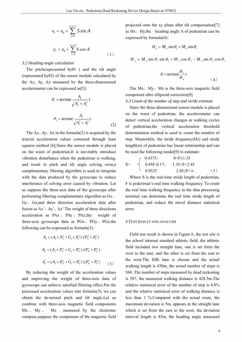
MPU3050 works in 2.1V ~ 3.6V low voltage, its built-in three-axis gyroscope can measure the direction of ± 250 ° / s ~ ± 2000 ° / s angular displacement.Editing the content of its register DLPF_FS can choose gyroscope’s working range, while the micro-controller read out the six-axis original data of registers X_OFFS_USRH / L, Y_OFFS_USRH / L, Z_OFFS_USRH / L through the IIC bus,and its peripheral circuits is shown in Figure 3.
期 The English Proceedings of the College of Instrumentation & Electrical Engineering, Jilin University, in the Second Half of 2013
8
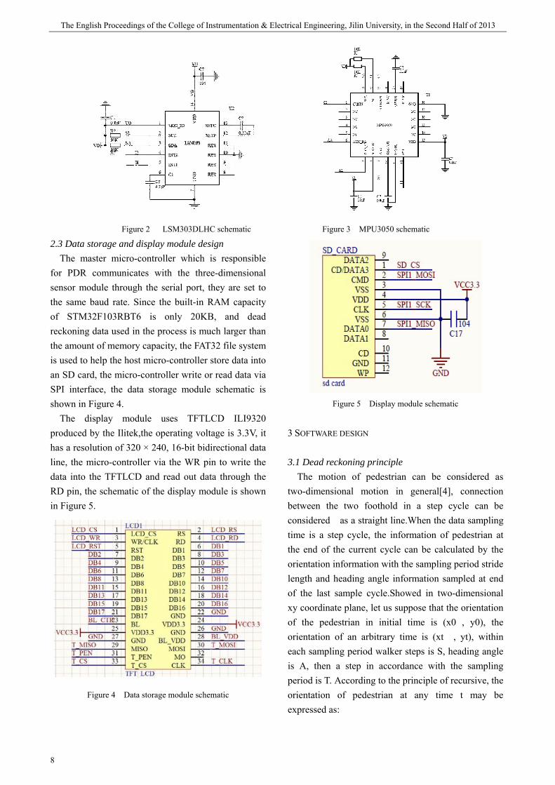
Figure 2 LSM303DLHC schematic Figure 3 MPU3050 schematic
2.3 Data storage and display module design The master micro-controller which is responsible
for PDR communicates with the three-dimensional sensor module through the serial port, they are set to the same baud rate. Since the built-in RAM capacity of STM32F103RBT6 is only 20KB, and dead reckoning data used in the process is much larger than the amount of memory capacity, the FAT32 file system is used to help the host micro-controller store data into an SD card, the micro-controller write or read data via SPI interface, the data storage module schematic is shown in Figure 4.
The display module uses TFTLCD ILI9320 produced by the Ilitek,the operating voltage is 3.3V, it has a resolution of 320 × 240, 16-bit bidirectional data line, the micro-controller via the WR pin to write the data into the TFTLCD and read out data through the RD pin, the schematic of the display module is shown in Figure 5.
Figure 4 Data storage module schematic
Figure 5 Display module schematic
3 SOFTWARE DESIGN
3.1 Dead reckoning principle The motion of pedestrian can be considered as
two-dimensional motion in general[4], connection between the two foothold in a step cycle can be considered as a straight line.When the data sampling time is a step cycle, the information of pedestrian at the end of the current cycle can be calculated by the orientation information with the sampling period stride length and heading angle information sampled at end of the last sample cycle.Showed in two-dimensional xy coordinate plane, let us suppose that the orientation of the pedestrian in initial time is (x0 , y0), the orientation of an arbitrary time is (xt , yt), within each sampling period walker steps is S, heading angle is A, then a step in accordance with the sampling period is T. According to the principle of recursive, the orientation of pedestrian at any time t may be expressed as:
Luo Yin etc.: Pedestrian Dead Reckoning Device Design Based on STM32
9
/
00
sinn t T
ti
x x S A=
=
= + ∑
∑=
=
+=Ttn
it ASxy
/
00 cos
(1)
3.2 Heading angle calculation The pitch(represented byθ1 ) and the tilt angle
(represented byθ2) of the sensor module calculated by the Ax, Ay, Az measured by the three-dimensional accelerometer can be expressed as[5]:
)arctan(221
zy
x
AAA+
=θ
)arctan(222
zx
y
AA
A
+=θ
(2)
The Ax、Ay、Az in the formula(2) is acquired by the triaxial acceleration values corrected through least squares method [6].Since the sensor module is placed on the waist of pedestrian.It is inevitably introduce vibration disturbance when the pedestrian is walking, and result in pitch and tilt angle solving error,a complementary filtering algorithm is used to integrate with the data produced by the gyroscope to reduce interference of solving error caused by vibration. Let us suppose the three-axis data of the gyroscope after performing filtering complementary algorithm as Gx、Gy、Gz,and three direction acceleration data after fusion as Ax’、Ay’、Az’ The weight of three directions acceleration as PAx 、 PAy 、 PAz,the weight of three-axis gyroscope data as PGx、PGy、PGz,the following can be expressed as formula(3):
)/()(' xG
xA
xGx
xAxx PPPGPAA +×+×=
)/()(' yG
yA
yGy
yAyy PPPGPAA +×+×=
)/()(' zG
zA
zGz
zAzz PPPGPAA +×+×= (3)
By reducing the weight of the acceleration values and improving the weight of three-axis data of gyroscope can achieve satisfied filtering effect.Put the processed acceleration values into formula(3), we can obtain the de-noised pitch and tilt angle.Let us combine with three-axis magnetic field components Mx 、 My 、 Mz measured by the electronic compass,suppose the component of the magnetic field
projected onto the xy plane after tilt compensation[7] as Hx、Hy,the heading angle A of pedestrian can be expressed by formula(4):
11 sinsin θθ zxx MMH +=
12212 cossincossinsin θθθθθ zyxy MMMH −+=
)arctan(y
x
HHA =
(4)
The Mx、My、Mz is the three-axis magnetic field component after ellipsoid correction[8]. 3.3 Count of the number of step and stride estimate
Since the three-dimensional sensor module is placed on the waist of pedestrian, the accelerometer can detect vertical acceleration changes in walking cycles of pedestrian,the vertical acceleration threshold determination method is used to count the number of step. Meanwhile, the stride frequency(Hz) and stride length(m) of pedestrian has linear relationship and can be used the following model[9] to estimate:
0.4375, 0<F≤1.35 S= 0.45F-0.17, 1.35<F<2.45
0.9325 2.45≤F<∞ (5) Where S is the real-time stride length of pedestrian,
F is pedestrian’s real time walking frequency. To count the real time walking frequency in the data processing terminal can determine the real time stride length of pedestrian, and reduce the travel distance statistical error.
4 TEST RESULT AND ANALYSIS
Field test result is shown in Figure 6, the test site is the school internal standard athletic field, the athletic field included two straight lane, one is set form the west to the east, and the other is set from the east to the west.The fifth lane is chosen and the actual walking length is 430m, the actual number of steps is 560 .The number of steps measured by dead reckoning is 587, the measured walking distance is 428.5m.The relative statistical error of the number of step is 4.8% and the relative statistical error of walking distance is less than 1 %.Compared with the actual route, the maximum deviation is 5m, appears in the straight lane which is set from the east to the west, the deviation interval length is 85m, the heading angle measured

期 The English Proceedings of the College of Instrumentation & Electrical Engineering, Jilin University, in the Second Half of 2013
10
error is ±2。~±4。or less. It is indicated that the above method designed walker dead reckoning device has a high accuracy, timeliness and reliability and meets the needs of practical application.
Figure 6 the test result schematic
5 EPILOGUE
The article describes the hardware and software algorithms design of the pedestrian dead reckoning device based on the micro-controller STM32F103RBT6, which completes the multi-sensor data acquisition and dead reckoning. The system which uses micro inertial devices and the micro-controller can meet the applicable requirement of miniaturization, practicality and portability and has the ease of setting up a system.Field experiments prove that the measurement accuracy can meet the actual demand.
References
[1] Lei Fang,Panos J. Antsaklis,Montestruque,Brett
McMickell,Design of a Wireless Assisted
Pedestrian Dead Reckoning System—The
NavMote Experience[J].IEEE TRANSACTIONS
ON INSTRUMENTATION AND
MEASUREMENT, 2005,12:2342-2355.
[2] Lauro Ojeda,Johann Borenstein, Non-GPS
Navigation with the Personal Dead-Reckoning
System[R].SPIE Defense and Security Conference,
Unmanned Systems Technology IX, Orlando,
Florida, April 9-13, 2007
[3] Sun Zuolei,Mao Xuchu,Zhang Xiangfen,Tian
Weifeng,The pedestrian positioning parameter
correction based on particle filtering and
probabilistic neural network[J].The Journal of
Shanghai Jiaotong University,2009,06:885-889
[4] Song Min,Shen Yanchun,Indoor Positioning dead
reckoning algorithm and implementation[J].
Computer Engineering,2013,07:294
[5] ST Corporation AN3182 Application Note[OL].
http:www.st.com/internet/com//TECHNICALLIT
ERATURE/DATASHEET/Doc ID 17289:13
[6] ST Corporation AN3182 Application Note[OL].
http:www.st.com/internet/com/TECHNICALRES
OUCES/TECHNICALLITERATURE/DATASHE
ET/Doc ID 17353:24
[7] ST Corporation AN3182 Application Note[OL].
http:www.st.com/internet/com/TECHNICALRES
OUCES/TECHNICALLITERATURE/DATASHE
ET/Doc ID 17353:7
[8] Chen Weitao,Zhang Yun,Electronic compass
design based on LSM303DLHC[OL].
http://www.paper.edu.cn/releasepaper/content/201
301-948:1-8
[9] Sun Zuolei,Mao Xuchu,Zhang Xiangfen,Tian
Weifeng,Pedestrian dead reckoning based on
motion recognition and stride estimation [J].The
Journal of Shanghai Jiaotong University, 2008,
12:2004
Xueyan hu etc.: Transit Passenger Flow Statistics System design
11
Transit Passenger Flow Statistics System design
Xueyan hu Lu bai Xingzhi han Abstract—Recently,the urban traffic jams in serious condition,bus as one of the most common means of transport is
overcrowded in the rush hour,on the other hand,it's nearly empty in times of traffic low.Moreover,faced with the situation
of buses dispatching at regular time, some people choose to buy their own cars,what made traffic in a worse
condition.Considering resolving this problem ,we designed a transit passenger flow statistics system, which would make a
reasonable provision of public transport resources, and then contribute to alleviating the pressure on traffic.Transit passenger
flow statistics system consist of transmitting part and receiving part.Transmitting part using Infrared Emitting Diode and
Photodiode calculators the passenger flow on the bus ,then acquired the current location and speed through GPS, and sent
these information to receiving part (i.e. the bus stops and Transit Company Dispatch Center) by wireless. The passengers
who was waiting at the site could observe operating conditions through the LCD of the bus stops ,in order that the
passengers would make the most rational choice, saving time to facilitate travel.Transit Company Dispatch Center would
schedule bus trips according to passenger flow conditions ,in that way could help conserve resources and satisfy transport
needs.
Keywords—bus;GPS;MSP430;people-counting; wireless communication
0 INTRODUCTION
THE present situation of the urban traffic is not optimistic,especially the peak commuting,in my opinion,in order to solve this situation,there are two ways to go,on the one hand,improving the situation of road and enhancing road construction,on the other hand,enhancing the management of road and improving use of existing resources.though the government is going on the first way,but there are a lot of works to do,relatively speaking,the second way can remit current situation quickly and effectively,so this passage do a research about the second way.current bus is a great resource,if we can use it effectively,it will improve the current situation obviously,as the same time,we can achieve the energy conservation and emission reduction,intelligent transportation system is the only way which is passed in the future.if there are enough loose and comfortable bus, i think people will choose bus but not private car, in order to intelligent transportation system, people counting and scheduling is very important.
1THE OVERALL DESIGN OF THE PROJECT
Transit Passenger Flow Statistics System is
consist of radiating portion and receiving portion. Radiating portion is used in the bus to achieve
people counting,to get the current speed and location by GPS,and send the information to the receiving portion, receiving portion shows the message by LCD to allow the passenger to choose the best way,the overall block diagram show as Figure 1.
Figure 1.the overall block diagram
2 ACHIEVEMENT AND ARRANGEMENT OF PARTS
2.1 radiating circuit module: Radiating circuit module includes MSP430F169
PCB,GPS module,radiating circuit and double red

期 The English Proceedings of the College of Instrumentation & Electrical Engineering, Jilin University, in the Second Half of 2013
12
outside to the tube 。GPS module and wireless module gear into MSP430 by serial port,radiating circuit module show as figure 2.
Figure 2.circuit of radiating module
2.2 receiving portion Receiving module includes MS430F149
PCB,wireless module,LCD circuit,LCD is controlled by parallel port,wireless module connect to serial port ,receiving module circuit show as figure 3.
P2.5/ROSC/CA525 P2.4/CA1/TA224 P2.3/CA0/TA123 P2.2/CAOUT/TA0/CA422 P2.1/TAINCLK/CA321 P2.0/ACLK/CA220
P1.2/TA114 P1.1/TA013 P1.0/TACLK/CAOUT12
P1.3/TA215
P1.4/SMCLK16
P1.7/TA219 P1.6/TA118 P1.5/TA017
P2.6/ADC12CLK/CA626
P2.7/TA0/CA727
P3.0/UCB0STE/UCA0CLK28
P3.1/UCB0SIMO/UCB0SDA29
P3.2/UCB0SOMI/UCB0SCL30
P3.3/UCB0CLK/UCA0STE31
P3.4/UCA0TXD/UCA0SIMO32
P3.5/UCA0RXD/UCA0SOMI33
P3.6/UCA1TXD/UCA1SIMO34
P3.7/UCA1RXD/UCA1SOMI35
P4.5/TB5 41P4.4/TB4 40P4.3/TB3 39P4.2/TB2 38P4.1/TB1 37P4.0/TB0 36
P4.6/TB6 42
P4.7/TBCLK 43
AVCC 64
AVSS 62
P5.0/UCB1STE/UCA1CLK 44
P5.1/UCB1SIMO/UCB1SDA 45
P5.2/UCB1SOMI/UCB1SCL 46
P5.3/UCB1CLK/UCA1STE 47
P5.4/MCLK 48
P5.5/SMCLK 49
P5.6/ACLK 50
P5.7/TBOUTH/SVSOUT 51
P6.0/A0 59
P6.1/A1 60
P6.2/A2 61
P6.3/A3 2
P6.4/A4 3
P6.5/A5 4
P6.6/A6 5
P6.7/A7/SVSIN 6
XT2OUT52
XT2IN53
RST/NMI58
TCK57
TDI/TCLK55
TMS56
VEREF+ 10
VREF+ 7
XIN 8
XOUT 9
TDO/TDI54
VREF-/VEREF- 11
U1
MSP430F249
CS1
1C
S22
GN
D3
VC
C4
V05
RS
6R
/W7
E8
DB0
9D
B110
DB2
11D
B312
DB4
13D
B514
DB6
15D
B716
RST
17-V
out
18
LCD1AMPIRE128X64
Figure 3.circuit of receiving module
3 SOFTWARE DESIGN
Software includes receiving portion and radiating portion. 3.1 radiating portion
Tasks of radiating portion are people counting,GPS Map,speed measurement、 send data.flow chart of radiating portion show as figure 4.
Figure 4.flow chart of radiating portion
3.1.1 people counting module people counting module consist of red outside to
the tube,it`s output voltage is high when people pass,on the contrary ,it`s output voltage is low,flow chart of people counting module show as figure 5.
Figure 5.flow chart of people counting module
3.1.2 GPS module The key of using of GPS module is to formulate
the communication protocol of Serial port,it includes
Xueyan hu etc.: Transit Passenger Flow Statistics System design
13
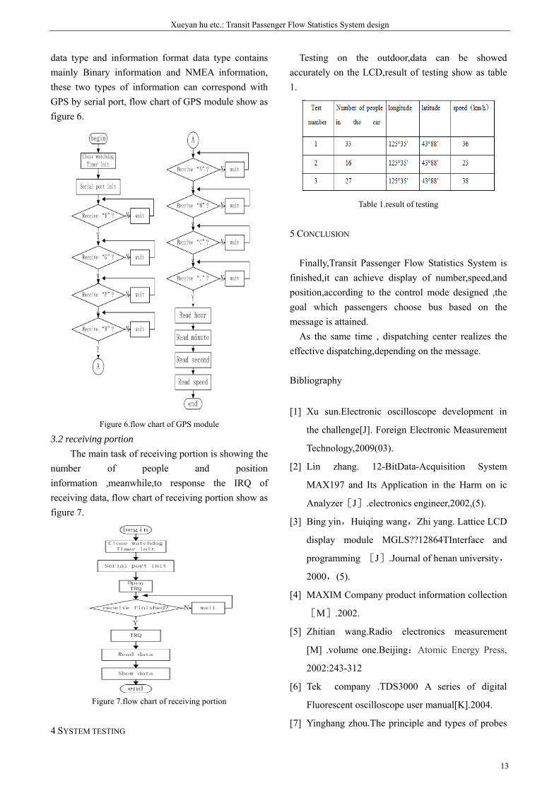
data type and information format data type contains mainly Binary information and NMEA information, these two types of information can correspond with GPS by serial port, flow chart of GPS module show as figure 6.
Figure 6.flow chart of GPS module
3.2 receiving portion The main task of receiving portion is showing the
number of people and position information ,meanwhile,to response the IRQ of receiving data, flow chart of receiving portion show as figure 7.
Figure 7.flow chart of receiving portion
4 SYSTEM TESTING
Testing on the outdoor,data can be showed accurately on the LCD,result of testing show as table 1.
Table 1.result of testing
5 CONCLUSION
Finally,Transit Passenger Flow Statistics System is finished,it can achieve display of number,speed,and position,according to the control mode designed ,the goal which passengers choose bus based on the message is attained.
As the same time , dispatching center realizes the effective dispatching,depending on the message.
Bibliography
[1] Xu sun.Electronic oscilloscope development in
the challenge[J]. Foreign Electronic Measurement
Technology,2009(03).
[2] Lin zhang. 12-BitData-Acquisition System
MAX197 and Its Application in the Harm on ic
Analyzer[J].electronics engineer,2002,(5).
[3] Bing yin,Huiqing wang,Zhi yang. Lattice LCD
display module MGLS??12864TInterface and
programming [J].Journal of henan university,
2000,(5).
[4] MAXIM Company product information collection
[M].2002.
[5] Zhitian wang.Radio electronics measurement
[M] .volume one.Beijing:Atomic Energy Press,
2002:243-312
[6] Tek company .TDS3000 A series of digital
Fluorescent oscilloscope user manual[K].2004.
[7] Yinghang zhou.The principle and types of probes

期 The English Proceedings of the College of Instrumentation & Electrical Engineering, Jilin University, in the Second Half of 2013
14
[K].2006.
[8] Fisherpan.Show you know oscilloprobe[K].2010.
[9] Zhongyi zhao.Principle of oscilloscope 、
Maintenance and calibration[M].Beijing :
Electronic Industry Press,1990:89-106
[10] Dongzhuo liu.Electronic measurement skills
training[K].2005.
[11] Shifu fan.Scientific instruments, live online
application development trend.Modern Scientific
Instruments [K]2009.
[12] Tianxudu,Bolin xie.phylogeny of instrument.
Journal of Chongqing University of Artsand
Sciences 28(4).
[13] Shenlin wen.Physical experiment[M],Guangzhou:
South China university of technology press,1991.
[14] Chengzhou ji.The basic knowledge of electronic
oscillograph[J],physics,1975(06).
[15] Wuhan University《electronic circuit》Teaching
Materials Writing Group.electronic circuit[M],
Beijing:People's Education Press,1979.
Li Na etc.: Design and Implementation of the full range of sub-control intelligent lighting system
15
Design and Implementation of the full range of sub-control intelligent lighting system
Li Na; Zhang Tao; Ye Jiansong
(College of Instrumentation and Electrical Engineering, Jilin University ,Changchun 130021,China) Abstract—In order to create a good lighting environment, making full use of the outside natural light to control dynamic
lights with low power consumption and intelligent characteristics, the intelligent lighting control system is based on the
STC89C51RC single-chip microcontroller as the processor, composed of light intensity sensor module, LED module and LED
drive circuits. It can automatically adjust the brightness supplemented by the outside light intensity, saving energy and
realizing sub-regional control functions. The detection accuracy of light intensity is less than 1.0 lx, adjusting time is less than
2.0 s, through actual measurement. Compared with ordinary fluorescent lamp, energy saving can rate up from 25% to 30%.
Key words—Lighting system; Light intensity sensor; Partition control; Low power consumption; Energy saving
0 PREFACE
THE intelligence of traditional lighting systems is quite low, with uncontinuous lighting control, short longevity and low energy conversion efficiency; besides, in some public places, such as classrooms, the use of light is often in unattended or poor management situation, which not only affects people's lives, but also is a great waste of power. This paper mainly introduces a design of a modular lighting system able to monitor external light intensity in full directions by each angle anytime and adjust its brightness automatically. This system uses the sub-regional controlled manner. Each region can detect the light intensity outside automatically, and the microcontroller control system processes the information, then send signals to the controlling system, which will adjust the number of lights and then adjust the brightness so as to meet general lighting requirements[1]. This lighting system can not only meet the requirement of normal life and work light intensity ,but the system can automatically adjust its brightness to facilitate the monitoring and management of public places.
This system selects the LED as light source. LED is called the fourth generation of green light source. Its emitting device is cold light source with low energy consumption, long longevity and other characteristics. In the case of the same lighting, the power consumption of LED lamp is one-tenth of an
incandescent lamp, half of a fluorescent. Compared with other lighting fixtures, LED lights contain no sodium, mercury and other elements which will do harm to people’s health and thus can protect environment to some degree[2]
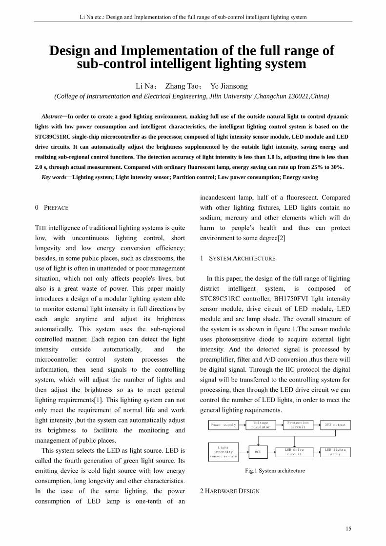
1 SYSTEM ARCHITECTURE
In this paper, the design of the full range of lighting district intelligent system, is composed of STC89C51RC controller, BH1750FVI light intensity sensor module, drive circuit of LED module, LED module and arc lamp shade. The overall structure of the system is as shown in figure 1.The sensor module uses photosensitive diode to acquire external light intensity. And the detected signal is processed by preamplifier, filter and A\D conversion ,thus there will be digital signal. Through the IIC protocol the digital signal will be transferred to the controlling system for processing, then through the LED drive circuit we can control the number of LED lights, in order to meet the general lighting requirements.
Fig.1 System architecture
2 HARDWARE DESIGN
期 The English Proceedings of the College of Instrumentation & Electrical Engineering, Jilin University, in the Second Half of 2013
16
2.1 System Controlling Structures Controlling systems are generally divided into the
closed loop control system and open-loop control system. In this design, light intensity signal collected requires feedback regulation so we choose closed loop control system[3]. System structure is shown in Figure 2.
Fig.2 System Control Structures
2.2 The main controlling module This system uses STC89C51RC microcontroller as
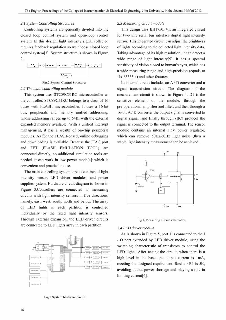
the controller. STC89C51RC belongs to a class of 16 buses with FLASH microcontroller. It uses a 16-bit bus, peripherals and memory unified addressing, whose addressing ranges up to 64K, with the external expanded memory available. With a unified interrupt management, it has a wealth of on-chip peripheral modules. As for the FLASH-based, online debugging and downloading is available. Because the JTAG port and FET (FLASH EMULATION TOOL) are connected directly, no additional simulation tools are needed .it can work in low power mode[4], which is convenient and practical to use.
The main controlling system circuit consists of light intensity sensor, LED driver modules, and power supplies system. Hardware circuit diagram is shown in Figure 3.Controllers are connected to measuring circuits with light intensity sensors in five directions, namely, east, west, south, north and below. The array of LED lights in each partition is controlled individually by the fixed light intensity sensors. Through external expansion, the LED driver circuits are connected to LED lights array in each partition.
Fig.3 System hardware circuit
2.3 Measuring circuit module This design uses BH1750FVI, an integrated circuit
for two-wire serial bus interface digital light intensity sensor. This integrated circuit can adjust the brightness of lights according to the collected light intensity data. Taking advantage of its high resolution ,it can detect a wide range of light intensity[5]. It has a spectral sensitivity of vision closed to human’s eyes, which has a wide measuring range and high-precision (equals to 1lx-65535lx) and other features.
Its internal circuit includes an A / D converter and a signal transmission circuit. The diagram of the measurement circuit is shown in Figure 4. D1 is the sensitive element of the module, through the pre-operational amplifier and filter, and then through a 16-bit A / D converter the output signal is converted to digital signal ,and finally through (IIC) protocol the signal is connected to the output terminal. The sensor module contains an internal 3.3V power regulator, which can remove 50Hz/60Hz light noise ,then a stable light intensity measurement can be achieved.
Fig.4 Measuring circuit schematics
2.4 LED driver module As is shown in Figure 5, port 1 is connected to the I
/ O port extended by LED driver module, using the switching characteristic of transistors to control the LED lights. After testing the circuit, when there is a high level in the base, the output current is 1mA, meeting the designed requirement. Resistor R1 is 5K, avoiding output power shortage and playing a role in limiting current[6].
Li Na etc.: Design and Implementation of the full range of sub-control intelligent lighting system
17
Fig.5 LED Lamp driver circuit
2.5 LED lamp module According to the core concept of the design, that is,
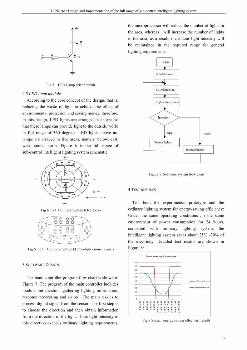
reducing the waste of light to achieve the effect of environmental protection and saving money, therefore, in this design, LED lights are arranged in an arc, so that these lamps can provide light to the outside world in full range of 360 degrees. LED lights above arc lamps are arrayed in five areas, namely, below, east, west, south, north. Figure 6 is the full range of sub-control intelligent lighting system schematic.
Fig.6(a)Outline structure (Overlook)
Fig.6(b) Outline structure (Three-dimensional visual)
3 SOFTWARE DESIGN
The main controller program flow chart is shown in Figure 7. The program of the main controller includes module initialization, gathering lighting information, response processing and so on . The main task is to process digital signal from the sensor. The first step is to choose the direction and then obtain information from the direction of the light. if the light intensity in this direction exceeds ordinary lighting requirements,
the microprocessor will reduce the number of lights in the area, whereas will increase the number of lights in the area; as a result, the indoor light intensity will be maintained in the required range for general lighting requirements.
Figure 7. Software system flow chart
4 TEST RESULTS
Test both the experimental prototype and the ordinary lighting system for energy-saving efficiency: Under the same operating conditions ,in the same environment of power consumption for 24 hours, compared with ordinary lighting system, the intelligent lighting system saves about 25% -30% of the electricity. Detailed test results are shown in Figure 8:
Fig.8 System energy saving effect test results

期 The English Proceedings of the College of Instrumentation & Electrical Engineering, Jilin University, in the Second Half of 2013
18
5 CONCLUSION
This paper mainly introduces the full range of intelligent lighting control system. Not only does the system accomplish real-time detection of ambient light intensity, but it also compensates for each other with the outside light intensity to adjust brightness automatically, which will meet the intelligent lighting requirements. Moreover, compared with the traditional lighting system, the intelligent lighting system has five partitions ,they are east, west, south, north and below, each of the LED lights array is equipped with a measuring circuit composed of light intensity sensors, five partitions are independent, realizing the purpose of sub-regional management. After actual test, regional recognition rates up to 100%; settling time is less than 2.0s; light intensity resolution is less than 1.0lx. Compared with ordinary lighting system ,the intelligent lighting system saves about 25% -30% of electricity in the same condition. In addition, the intelligent lighting system can achieve good energy saving effect, extending lamp longevity. All the advantages guarantee the intelligent lighting control system a promising market prospect.
References
[1] Wang Wensheng. Intelligent lighting control and
energy saving [J]. intelligent building and city
information.2005.
[2] Wang Xijuan LED intelligent lighting control
system. Automation of manufacturing industry,
2012, 33 (12): 128-131.
[3] Wang Chunmin, Liu Xingming, Ji Yan Ju.
Continuous and discrete control system. Jilin
University press,.2008:4-6.
[4] Yang Ping, Wang Wei.MSP430 series ultra low
power microcontroller [J]. foreign electronic
measurement technology.2008.
[5] Yun zhonghua, Bai tianrui. indoor illumination
intensity measuring instrument based on
BH1750FVI [J]. microcontroller and embedded
system application.2012
[6] Kang Huaguang. Electronic Technology (Analog).
Higher education press,.2006:116-118.
Pei Li-ran etc.: Research on wireless synchronization device in superficial seismic exploration
19
Research on wireless synchronization device in superficial seismic exploration
Zhang Lin-hang, Pei Li-ran, Sun Zi-chao, Wang Cong
(College of instrumentation and electrical engineering, Jilin University, Changchun 130061, China)
Abstract—In order to better solve the time synchronization problem of shallow seismic prospecting signal acquisition, Put
forward a data acquisition system of shallow seismic exploration based on wireless network.It uses AT89C51 micro-controller
as the main controller,Use AD7705 modulus conversion chip with low power consumption and high resolution to realize data
collection ,Choose nRF24L01 set up wireless network ,According to the characteristics of modulus conversion unit and
MCU ,Design the power module and the voltage stabilizing circuit to realize accurate flexible power supply.By determining
the real-time data of different transmission distance ,Use seismograph for time compensation thus realize data acquisition
synchronization .Solving the complex wiring and synchronization problems when the conditions for exploration,realizing
low-power,portable and synchronization function in the shallow seismic exploration.Tests show that the system power
consumption is 2500mW ,the wireless transmission distance is 94m, and transmission delay time is less than 1.87μs.
Key words—Instrument and meter technology; wireless Synchronous; prediction model; superficial seismic exploration;
data acquisition; Analog-to-digital conversion; Wireless synchronization .
INTRODUCTION
SHALLOW seismic exploration is the use of special detection equipment , record the artificial excitation seismic reflection and refraction , wave travel time,amplitude , waveform , in order to analyze and judge of a geophysical method formation interface of geotechnical and geological structure[1、2] . Shallow seismic exploration instruments are precision and key equipment for the most shallow seismic prospecting[3] . And the synchronization precision of data acquisition and wireless transmission technology has become an important index to measure the shallow seismic prospecting instrument. The measurement precision of time synchronization directly influences the quality of seismic observation records, is required for seismic data analysis and inversion of seismic wave valuable data[4]. With the poor and the exploration of shallow seismic exploration environment of the expansion[5], the cable telemetry seismic instrument mainstream in some degree , it is difficult to meet the actual needs, and requirements of shallow seismic exploration instrument must be light[6] . Radio telemetry seismic instrument not only reduces the field work burden, but also avoid the inherent large line crosstalk , antenna interference , frequency interference , so synchronization, wireless , portable[7] , low power
consumption is the key of system design.The more mature and widely used in wireless communication are mainly GPRs , WiFi , Imote2 , Zigbee , ultra wideband impulse , but can meet the design requirements of the few , such as the GPRS network , although can meet the communication distance requirements , but the communication speed is low,can not meet the requirements of rapid transmission of large amounts of seismic data the ; Although WiFi can meet the transmission speed requirements , but the real environment of radio interference too much , can not guarantee the accuracy of the data ; Imote2 can meet the wireless synchronous but complex protocol and is mainly applied to speed[8] Zigbee sensor network are slower and not through a barrier[9] ; Ultra wideband pulse wireless transmission distance , low power consumption and poor anti-interference ability , data and low accuracy[10、11].Integrated simple and portable , low power and wireless synchronization requirements , this study adopts nRF24L01 wireless module to realize wireless transmission based on detecting, and combined with the AD7705 analog to digital conversion using strain sensor , it not only has the real-time detection ability , and simple hardware , good stability; software algorithm is fast and efficient , the design has important significance for seismic data acquisition in shallow layer and wireless synchronization .

期 The English Proceedings of the College of Instrumentation & Electrical Engineering, Jilin University, in the Second Half of 2013
20
1 THE STRUCTURE OF THE OVERALL SYSTEM DESIGN
The system consists of detector data synchronous transmission system and acquisition terminal of the wireless synchronous receiving and processing system of two parts , the shallow layer seismic exploration , seismic
instrument control system , the hammer source signal is received by the detector data synchronous transmission system , through the wireless transmission to the acquisition terminal of the wireless synchronous receiving and processing system , start the seismograph began data acquisition . The overall structure block diagram is shown in figure 1 .
Detector data wireless synchronous transmission system will hammer source signal through the strain type pressure sensor circuit is converted to analog voltage signal , using A/D 16 to improve the signal acquisition , data processing precision , synchronous signal picked up by the wireless data transmission module based on nRF24L01 transmission in digital mode is more accurate , is the main part of the ensure the test signal and then measured data time synchronization reference ; acquisition terminal of the wireless synchronous receiving and processing system to receive the data wireless transmission system transmits the same step by using the nRF24L01 wireless data transmission module in exactly the same data , the wireless transmission, wireless transmission , relay and receiving delay , resulting in synchronization error , timing meter or oscilloscope through the calculation of a specific delay time , seismic instrument synchronization adjustment using the software compensation method , the error synchronizing signal to target .
2 DESIGN OF DATA ACQUISITION MODULE
Hammer source signal acquisition module plays an important role in the whole system. Amplification circuit, the anti-interference ability and stability directly
affect the acquisition to the accuracy of the data . The source signal acquisition module block diagram is shown in figure 2 .
Strain type pressure
transducer
The AT89C51 host controller
power-supply module;
A/D conversion
unit
Acquisition system consists of the strain
sensor , analog digital conversion module with AD7705 as the core and taking AT89C51 as the core of the main controller . 2.1 Design of A/D conversion circuit
Hammer source signal has a weak signal , amplitude is small , strong electromagnetic interference , low signal-to-noise ratio , the signal frequency is low , so the A/D circuit should have high gain , high input impedance , high CMRR characteristic .
Acquisition system using a small hammer as simulation source , using strain type pressure sensor converts the analog signal into voltage signal through the A/D conversion circuit , digital . The A/D conversion circuit using AD7705 chip , it has high resolution , wide
Fig. 2 Data acquisition system
Fig.1 The overall structure diagram
Pei Li-ran etc.: Research on wireless synchronization device in superficial seismic exploration
21
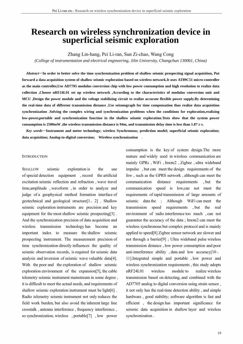
dynamic range , automatic calibration , noise , with 16 bit no missing codes; nonlinearity of 0.00003[12] ; Programmable gain , low power consumption and is with programmable amplifier and an on-chip digital filter for 16 bit sigma delta ADC . AD7705 through the serial clock input chip select CS, SCLK,
instructions or data input DIN and output DOUT conversion pin connected with the single chip microcomputer AT89C51. When the state signal DRDY output data register data is ready , the MCU reads the conversion results . AD7705 and MCU to connect the circuit shown in figure 3 as shown .
Fig. 3 AD7705 and single-chip computer connected to the circuit diagram
The AD7705 chip in 5V analog voltage , and by the AD780 2.5V reference voltage regulator chip provides Accurate, between analog voltage and electrolytic capacitors and ceramic capacitors in parallel to form a decoupling circuit ; in order to improve the update rate of sampling frequency , get higher data, the master clock frequency of AD7705 is set to 2.4576MHz ; in addition , AD7705 the integrated amplifier , filter circuit , no additional signal conditioning circuit. The acquisition system integrated, simple, to meet the system is small , portable design requirements .
3 THE DATA TRANSMISSION MODULE DESIGN
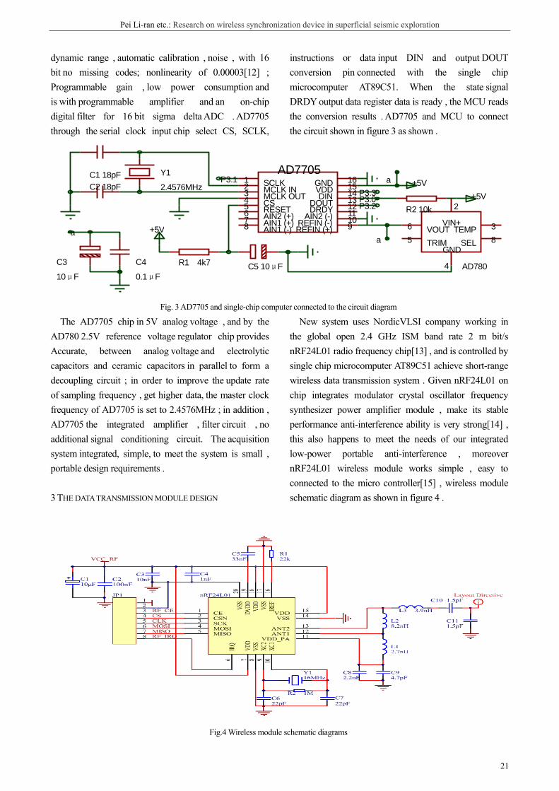
New system uses NordicVLSI company working in the global open 2.4 GHz ISM band rate 2 m bit/s nRF24L01 radio frequency chip[13] , and is controlled by single chip microcomputer AT89C51 achieve short-range wireless data transmission system . Given nRF24L01 on chip integrates modulator crystal oscillator frequency synthesizer power amplifier module , make its stable performance anti-interference ability is very strong[14] , this also happens to meet the needs of our integrated low-power portable anti-interference , moreover nRF24L01 wireless module works simple , easy to connected to the micro controller[15] , wireless module schematic diagram as shown in figure 4 .
Fig.4 Wireless module schematic diagrams
P3.1P3.3P3.2
a a
a
P3.0
VIN+ 2
VOUT 6
GND 4
TEMP 3
TRIM 5 SEL 8
AD780
AIN1 (+)7
SCLK1MCLK IN2
AIN2 (+)6
MCLK OUT3CS4RESET5
AIN1 (-)8 REFIN (+) 9
VDD 15DIN 14
DOUT 13DRDY 12
AIN2 (-) 11
GND 16
REFIN (-) 10
AD7705Y1
2.4576MHz C1 18pF C2 18pF
R1 4k7 C5 10μF
+5V
R2 10k +5V
+5V
C3
10μF C4
0.1μF

期 The English Proceedings of the College of Instrumentation & Electrical Engineering, Jilin University, in the Second Half of 2013
22
Wireless including wireless sending and receiving two parts . When a hammer source signal on the sensor, the sensor quickly feel hammer signal, pressure signal can be converted to analog signals, and signal disposal by AD7705 digital signal will be sent to the main controller , wireless module is controlled by a master controller will be the source signal , a buzzer and LED to successfully sent by sound and light signals such as prompt ; The receive module , real time, when the received signal after first by judging whether the source signal from the controller and then data processing , a successful acousto-optic hint at the same time . Wireless transmission part of the program flow chart is shown in figure 5 .
Fig.5 Wireless transmission part of the program flow chart
4 SYSTEM TEST
Test method : The whole system is tested by the sending and receiving of two parts , the sending end and receiving end of two signals through the length of shielding line is connected to the two input channel of the oscilloscope , he two signal shielding in to the oscilloscope before the line length , layout is identical , transmission time difference between the two signal
to oscilloscope ignored , by the oscilloscope observation delay time signal waveform is the time difference between the acquisition system . System test connection diagram as shown in figure 6 .
Overall test : When the hammer peening source signals
in the detectors, sending digital hammer source signals , and the buzzer sounds tips and receiving end of the indicating lamp is bright , and the received signal to the seismic instrument . The exploration of environmental uncertainty , the same environment different transmission distance or different circumstances the same transmission distance transmission effect is not the same , the precision of the synchronization time is not the same , determined by exploration environment and wireless transceiver distance , the design of data acquisition system of delay time is constant , the seismic instrument we can make the corresponding compensation according to the delay time measurement , so as to achieve the purpose of shallow seismic exploration of wireless synchronization purposes .
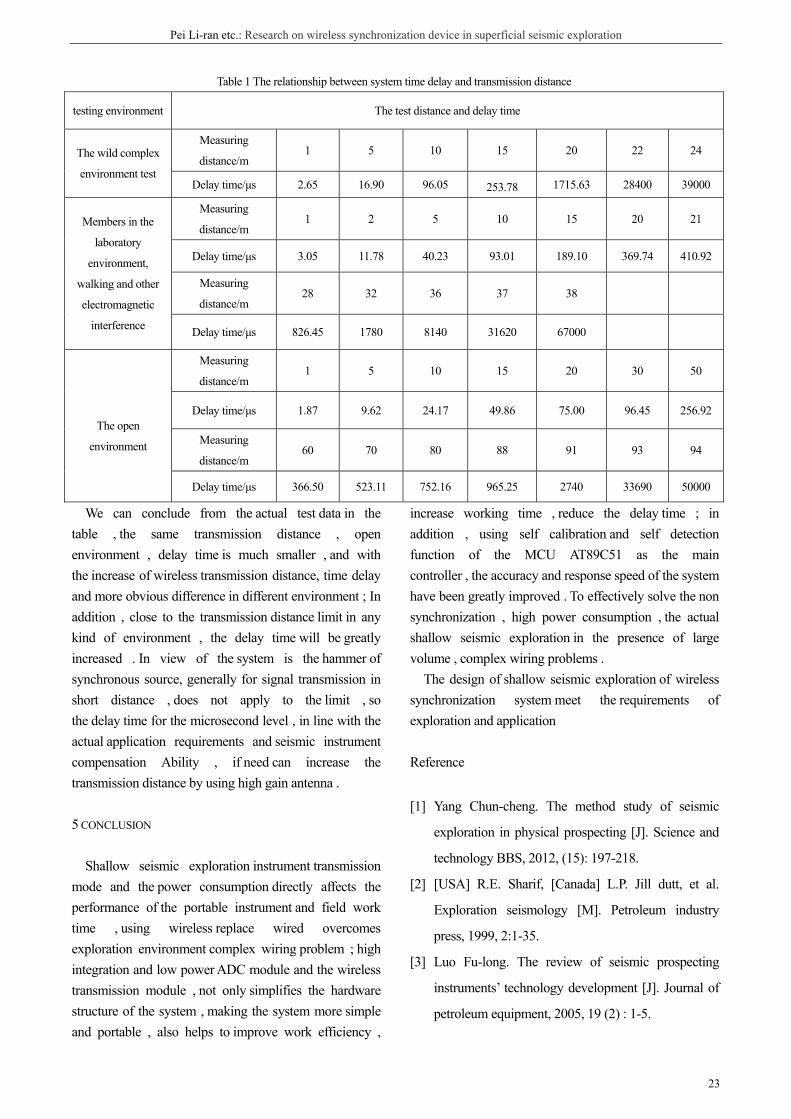
Test in an open environment , far transmission distance system reach 94m , the transmission delay time is 1.87 μ s-0.05s ; in a laboratory environment officers around and other electromagnetic wave interference , far transmission distance of the system is 38m , the delay time is 3.05 μ s-0.067s ; complex field environment , the distance of transmission up to a distance of about 24m , the delay time is 2.65 μ s-0.039s ; after determining the delay time under different environment system , the seismic instrument according to delay time compensation , so as to achieve synchronization . The different environment , The relationship between system time delay and transmission distance as shown in table 1 .
Fig. 6 System -test connection diagram
Pei Li-ran etc.: Research on wireless synchronization device in superficial seismic exploration
23
Table 1 The relationship between system time delay and transmission distance
testing environment The test distance and delay time
Measuring
distance/m 1 5 10 15 20 22 24 The wild complex
environment test Delay time/μs 2.65 16.90 96.05 253.78 1715.63 28400 39000
Measuring
distance/m 1 2 5 10 15 20 21
Delay time/μs 3.05 11.78 40.23 93.01 189.10 369.74 410.92
Measuring
distance/m 28 32 36 37 38
Members in the
laboratory
environment,
walking and other
electromagnetic
interference Delay time/μs 826.45 1780 8140 31620 67000
Measuring
distance/m 1 5 10 15 20 30 50
Delay time/μs 1.87 9.62 24.17 49.86 75.00 96.45 256.92
Measuring
distance/m 60 70 80 88 91 93 94
The open
environment
Delay time/μs 366.50 523.11 752.16 965.25 2740 33690 50000
We can conclude from the actual test data in the table , the same transmission distance , open environment , delay time is much smaller , and with the increase of wireless transmission distance, time delay and more obvious difference in different environment ; In addition , close to the transmission distance limit in any kind of environment , the delay time will be greatly increased . In view of the system is the hammer of synchronous source, generally for signal transmission in short distance , does not apply to the limit , so the delay time for the microsecond level , in line with the actual application requirements and seismic instrument compensation Ability , if need can increase the transmission distance by using high gain antenna .
5 CONCLUSION
Shallow seismic exploration instrument transmission mode and the power consumption directly affects the performance of the portable instrument and field work time , using wireless replace wired overcomes exploration environment complex wiring problem ; high integration and low power ADC module and the wireless transmission module , not only simplifies the hardware structure of the system , making the system more simple and portable , also helps to improve work efficiency ,
increase working time , reduce the delay time ; in addition , using self calibration and self detection function of the MCU AT89C51 as the main controller , the accuracy and response speed of the system have been greatly improved . To effectively solve the non synchronization , high power consumption , the actual shallow seismic exploration in the presence of large volume , complex wiring problems .
The design of shallow seismic exploration of wireless synchronization system meet the requirements of exploration and application
Reference
[1] Yang Chun-cheng. The method study of seismic
exploration in physical prospecting [J]. Science and
technology BBS, 2012, (15): 197-218.
[2] [USA] R.E. Sharif, [Canada] L.P. Jill dutt, et al.
Exploration seismology [M]. Petroleum industry
press, 1999, 2:1-35.
[3] Luo Fu-long. The review of seismic prospecting
instruments’ technology development [J]. Journal of
petroleum equipment, 2005, 19 (2) : 1-5.

期 The English Proceedings of the College of Instrumentation & Electrical Engineering, Jilin University, in the Second Half of 2013
24
[4] Ren Jia-fu, Li Huai-liang, Tao Yong-li. Study of
wireless synchronization seismic data acquisition
technology[J]. China measurement technology, 2008,
34 (15):1-3.
[5] Li Tai-quan, Sun Xian-song. Low-power design of
shallow seismograph based on wireless network[J].
Journal of electronic measurement technology, 2012,
35 (12) : 28-34.
[6] Li Huai-liang, Du Xian-guo, Du Yong, et al. Study
of telemetric seismic data acquisition technique
base onwireless communication[J]. Chinese
geophysics, 2011, (16): 519.
[7] Zhang Lin-hang.Study on Data Transmission
Techniques Based on Relay Ethernet in Seismic
Exploration using Vibroseis[D]. Changchun: Jilin
University, 2007.
[8] Lu Hui, Shen Qing-hong, Chen Ce,et al. Wireless
Transmission of WSN Bridge Health Monitoring
System Based on Imote2[J]. Now electronic
technology, 2010, (21): 30-34.
[9] Li Su-yi, Zhang Hong-Jing, Lu Xia, et al. Wireless
Dynamic ECG Monitoring System Based on ZigBee
Technology[J]. Journal of Jilin university
(information science edition), 2012, 30 (5):451-455.
[10] Xu Bin, Bi Guang-guo. Discussion on
ultra-wideband pulse wireless transmission
technology [N]. Computer World, 2004-10-11(B06).
[11] Tang Lan, Wang Shu-xun, Sun Xiao-ying, et al. Ultra
broadband wireless transmission technology [J],
Journal of Jilin University (Engineering and
Technology Edition), 2004,34(2):331-334.
[12] Yang Lei.The The Research of the FPGA-Based
Data Collection system of Respirator [D].
Changchun: Jilin University, 2006.
[13] Wang Shun, Gu Ye-dan, MCU application design of
wireless network based on nRF24L01[J]. Journal
of instruments and meters, 2010, 31 (8): 55 to 57.
[14] Wei Ji-hui. Design and Implementation of Wireless
Network Based on nRF24L01 [D]. Jilin: Jilin
University, 2012.
[15] Wang Sheng-yuan, Zhang Hong-wu, zhao kai, et al.
Design and Realization of Wireless Transceiver
Module in Communication of Many Machines[J].
Journal of Jilin university (science edition), 2006, 44
(3): 470-472.
Shi Zhaomin etc.: The Research of Sphere Lifting Height Automatic Control System Based on Air Pressure Control
25
The Research of Sphere Lifting Height Automatic Control System Based on Air Pressure Control
Qian Chenghui ;Shi Zhaomin;Kang Lili; Li Qi
(College of Instrumentation&Electrical Engineering,JilinUniversity,Changchun 130022,China) Abstract—For precise control of sphere lifting height in the pipeline, this paper puts forward to a better way to regulate sphere
lifting height based on the control of pressure automatic regulating’s principle. MCU changes the rotation moving angle of the
stepper motor to manage the pipeline pressure change. The test result shows that the system can set lifting height、residence time、
the order of spherical movement, send control information via wireless communication and display spherical height and error
information continuously. The relative error is 1.45%. With the movements of sphere,it reflects the status of the pipeline’s pressure.
This system has good application prospect in the physics experimental teaching.
Key words—Air pressure valve; Sphere lifting height control; Experimental teaching
0 INTRODUCTION
AT present, with the development of electronic products and electronic technology, physics teaching demonstrates related physical phenomena to students through related animation to help them understand and learn. Although animation image, screen demonstration of the ideal situation is not conducive to cause the students to understand and think for the reality of the physical phenomena. According to illustrate vividly pressure meaning problem, the author designed a sphere lifting height automatic control system based on air pressure control. For pure pneumatic control system, the complexity is higher and the corresponding costs are bigger [1].It’s not suitable for the promotion of laboratory teaching. In order to save the cost, we adopt the combination of pneumatic technology and electric technology to complete the design
Pressure control system has some advantages such as fast signal transmission, high transmission efficiency and so on. But its adjustment range and adjustment precision is lower than the same degree of hydraulic control system. At the same time, the noise is larger and the smooth degree is low [2]. To make up for the shortage above, system adopts pneumatic control, combines step motor and pneumatic valve to closed loop network, to enhance the accuracy of the system. One light sphere goes through the system, and the ball movement reflects pressure state, vividly and maneuverably.
1 THE SYSTEM HARDWARE DESIGN
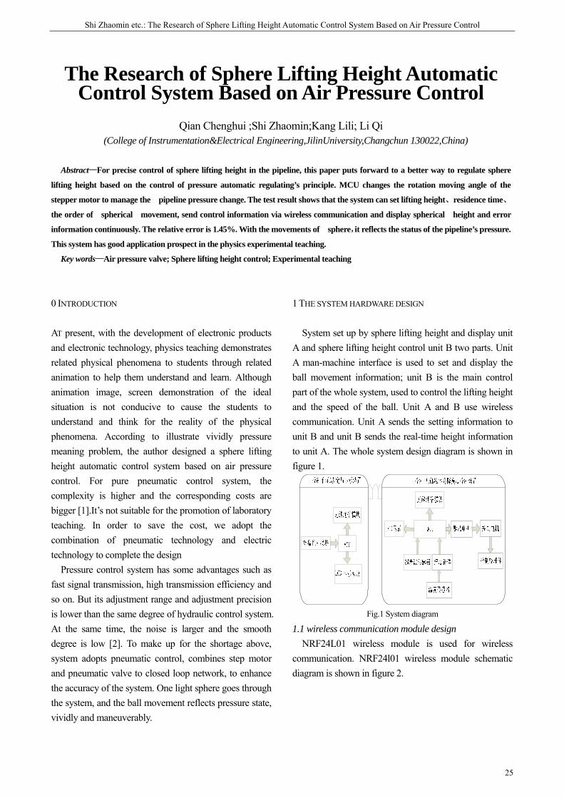
System set up by sphere lifting height and display unit A and sphere lifting height control unit B two parts. Unit A man-machine interface is used to set and display the ball movement information; unit B is the main control part of the whole system, used to control the lifting height and the speed of the ball. Unit A and B use wireless communication. Unit A sends the setting information to unit B and unit B sends the real-time height information to unit A. The whole system design diagram is shown in figure 1.
Fig.1 System diagram
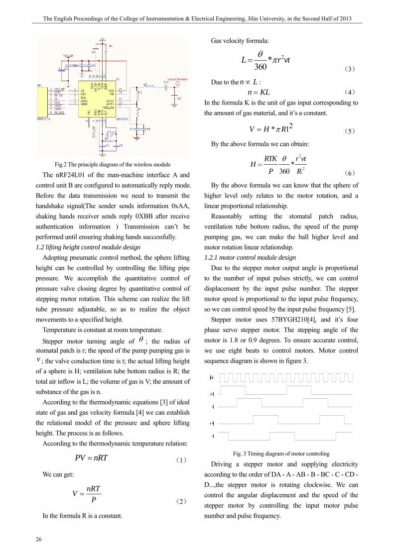
1.1 wireless communication module design NRF24L01 wireless module is used for wireless
communication. NRF24l01 wireless module schematic diagram is shown in figure 2.
期 The English Proceedings of the College of Instrumentation & Electrical Engineering, Jilin University, in the Second Half of 2013
26
Fig.2 The principle diagram of the wireless module
The nRF24L01 of the man-machine interface A and control unit B are configured to automatically reply mode. Before the data transmission we need to transmit the handshake signal(The sender sends information 0xAA, shaking hands receiver sends reply 0XBB after receive authentication information ) Transmission can’t be performed until ensuring shaking hands successfully. 1.2 lifting height control module design
Adopting pneumatic control method, the sphere lifting height can be controlled by controlling the lifting pipe pressure. We accomplish the quantitative control of pressure valve closing degree by quantitative control of stepping motor rotation. This scheme can realize the lift tube pressure adjustable, so as to realize the object movements to a specified height.
Temperature is constant at room temperature.
Stepper motor turning angle of θ ; the radius of stomatal patch is r; the speed of the pump pumping gas is v ; the valve conduction time is t; the actual lifting height of a sphere is H; ventilation tube bottom radius is R; the total air inflow is L; the volume of gas is V; the amount of substance of the gas is n.
According to the thermodynamic equations [3] of ideal state of gas and gas velocity formula [4] we can establish the relational model of the pressure and sphere lifting height. The process is as follows.
According to the thermodynamic temperature relation:
PV nRT= (1)
We can get:
nRTVP
= (2)
In the formula R is a constant.
Gas velocity formula:
2*360
L r vtθ π= (3)
Due to the n L∝ : n KL= (4)
In the formula K is the unit of gas input corresponding to the amount of gas material, and it’s a constant.
2* 1π=V H R (5)
By the above formula we can obtain: 2
21
*360
θ=
RTK r vtH
P R (6)
By the above formula we can know that the sphere of higher level only relates to the motor rotation, and a linear proportional relationship.
Reasonably setting the stomatal patch radius, ventilation tube bottom radius, the speed of the pump pumping gas, we can make the ball higher level and motor rotation linear relationship. 1.2.1 motor control module design
Due to the stepper motor output angle is proportional to the number of input pulses strictly, we can control displacement by the input pulse number. The stepper motor speed is proportional to the input pulse frequency, so we can control speed by the input pulse frequency [5].
Stepper motor uses 57BYGH210[4], and it’s four phase servo stepper motor. The stepping angle of the motor is 1.8 or 0.9 degrees. To ensure accurate control, we use eight beats to control motors. Motor control sequence diagram is shown in figure 3.
Fig. 3 Timing diagram of motor controling
Driving a stepper motor and supplying electricity according to the order of DA - A - AB - B - BC - C - CD - D...,the stepper motor is rotating clockwise. We can control the angular displacement and the speed of the stepper motor by controlling the input motor pulse number and pulse frequency.
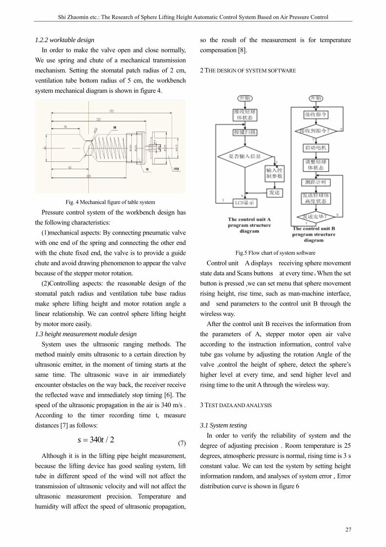
Shi Zhaomin etc.: The Research of Sphere Lifting Height Automatic Control System Based on Air Pressure Control
27
1.2.2 worktable design In order to make the valve open and close normally,
We use spring and chute of a mechanical transmission mechanism. Setting the stomatal patch radius of 2 cm, ventilation tube bottom radius of 5 cm, the workbench system mechanical diagram is shown in figure 4.
Fig. 4 Mechanical figure of table system
Pressure control system of the workbench design has the following characteristics:
(1)mechanical aspects: By connecting pneumatic valve with one end of the spring and connecting the other end with the chute fixed end, the valve is to provide a guide chute and avoid drawing phenomenon to appear the valve because of the stepper motor rotation.
(2)Controlling aspects: the reasonable design of the stomatal patch radius and ventilation tube base radius make sphere lifting height and motor rotation angle a linear relationship. We can control sphere lifting height by motor more easily. 1.3 height measurement module design
System uses the ultrasonic ranging methods. The method mainly emits ultrasonic to a certain direction by ultrasonic emitter, in the moment of timing starts at the same time. The ultrasonic wave in air immediately encounter obstacles on the way back, the receiver receive the reflected wave and immediately stop timing [6]. The speed of the ultrasonic propagation in the air is 340 m/s . According to the timer recording time t, measure distances [7] as follows:
340 / 2=s t (7)
Although it is in the lifting pipe height measurement, because the lifting device has good sealing system, lift tube in different speed of the wind will not affect the transmission of ultrasonic velocity and will not affect the ultrasonic measurement precision. Temperature and humidity will affect the speed of ultrasonic propagation,
so the result of the measurement is for temperature compensation [8].
2 THE DESIGN OF SYSTEM SOFTWARE
Fig.5 Flow chart of system software
Control unit A displays receiving sphere movement state data and Scans buttons at every time。When the set button is pressed ,we can set menu that sphere movement rising height, rise time, such as man-machine interface, and send parameters to the control unit B through the wireless way.
After the control unit B receives the information from the parameters of A, stepper motor open air valve according to the instruction information, control valve tube gas volume by adjusting the rotation Angle of the valve ,control the height of sphere, detect the sphere’s higher level at every time, and send higher level and rising time to the unit A through the wireless way.
3 TEST DATA AND ANALYSIS
3.1 System testing In order to verify the reliability of system and the
degree of adjusting precision . Room temperature is 25 degrees, atmospheric pressure is normal, rising time is 3 s constant value. We can test the system by setting height information random, and analyses of system error , Error distribution curve is shown in figure 6
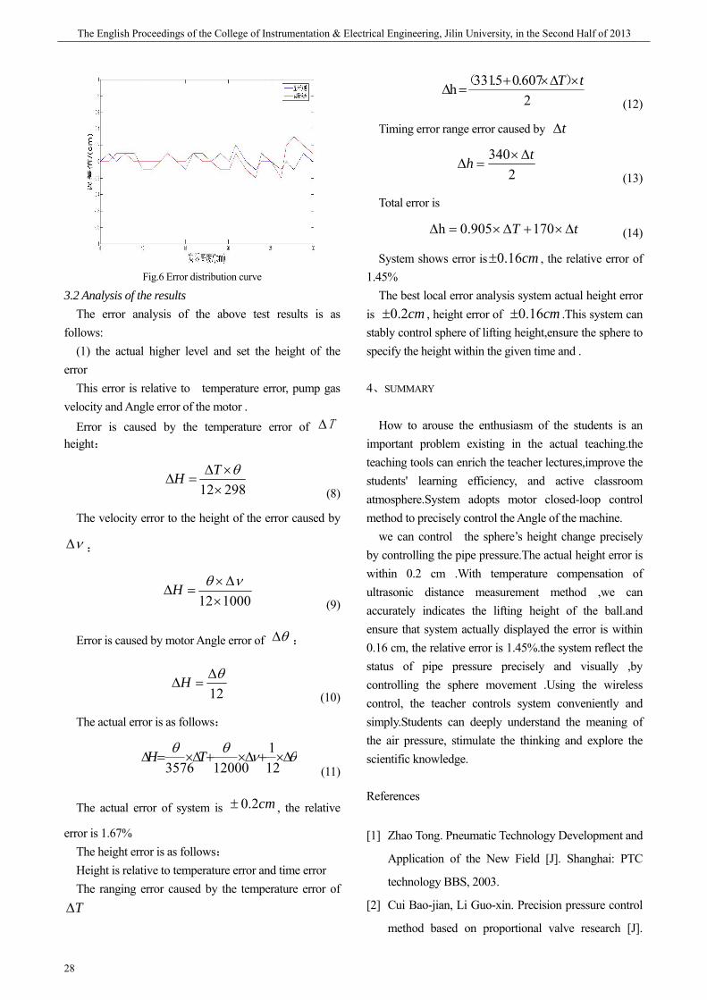
期 The English Proceedings of the College of Instrumentation & Electrical Engineering, Jilin University, in the Second Half of 2013
28
Fig.6 Error distribution curve
3.2 Analysis of the results The error analysis of the above test results is as
follows: (1) the actual higher level and set the height of the
error This error is relative to temperature error, pump gas
velocity and Angle error of the motor . Error is caused by the temperature error of TΔ
height:
29812××Δ
=ΔθTH
(8)
The velocity error to the height of the error caused by
νΔ :
100012×Δ×
=ΔνθH
(9)
Error is caused by motor Angle error of θΔ :
12θΔ
=ΔH (10)
The actual error is as follows:
θνθθΔ×+Δ×+Δ×=Δ
121
120003576TH
(11)
The actual error of system is cm2.0± , the relative
error is 1.67% The height error is as follows: Height is relative to temperature error and time error The ranging error caused by the temperature error of TΔ
2607.05.331h tT ×Δ×+
=Δ)(
(12)
Timing error range error caused by tΔ
2340 th Δ×
=Δ (13)
Total error is
tT Δ×+Δ×=Δ 170905.0h (14)
System shows error is 0.16cm± , the relative error of 1.45%
The best local error analysis system actual height error is 0.2cm± , height error of 0.16cm± .This system can stably control sphere of lifting height,ensure the sphere to specify the height within the given time and .
4、SUMMARY
How to arouse the enthusiasm of the students is an important problem existing in the actual teaching.the teaching tools can enrich the teacher lectures,improve the students' learning efficiency, and active classroom atmosphere.System adopts motor closed-loop control method to precisely control the Angle of the machine.
we can control the sphere’s height change precisely by controlling the pipe pressure.The actual height error is within 0.2 cm .With temperature compensation of ultrasonic distance measurement method ,we can accurately indicates the lifting height of the ball.and ensure that system actually displayed the error is within 0.16 cm, the relative error is 1.45%.the system reflect the status of pipe pressure precisely and visually ,by controlling the sphere movement .Using the wireless control, the teacher controls system conveniently and simply.Students can deeply understand the meaning of the air pressure, stimulate the thinking and explore the scientific knowledge.
References
[1] Zhao Tong. Pneumatic Technology Development and
Application of the New Field [J]. Shanghai: PTC
technology BBS, 2003.
[2] Cui Bao-jian, Li Guo-xin. Precision pressure control
method based on proportional valve research [J].

Shi Zhaomin etc.: The Research of Sphere Lifting Height Automatic Control System Based on Air Pressure Control
29
Beijing: the computer measurement and control.
2005-12.
[3] Zhang San-hui, etc. The university physics,
thermodynamics, optics, quantum physics (3rd
edition) [M]. Beijing: tsinghua university press.
2009.
[4] Teng Xiao-ying, Douglas C.Giancoli. University
physics[M]. Higher education press. 2005.
[5] Zhu Xi-lin etc. Mechanical and electrical - body
design foundation [M]. Beijing: mechanical industry
publishing house. 1997.
[6] Huang Mao-lin, Qin Wei. Mechanical principle [M].
Beijing: mechanical industry publishing house. 2002.
[7] Yang Qing,Chen Gui-ming, Dong Zhen-qi. An
improved high accuracy ultrasonic distance
measurement method research [J]. Computer
technology and development. 2010.
[8] Wang Rong-rong, Yang Hai-zhong. Ultrasonic
ranging error compensation algorithm study [J].
Industrial automation. 2012.
[9] Zheng Di, Tang Ke-hong. Electromechanical
integration design [M]. Beijing: mechanical industry
publishing house, 1997
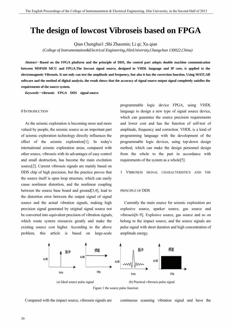
期 The English Proceedings of the College of Instrumentation & Electrical Engineering, Jilin University, in the Second Half of 2013
30
The design of lowcost Vibroseis based on FPGA
Qian Chenghui1 ;Shi Zhaomin; Li qi; Xu qian (College of Instrumentation&Electrical Engineering,JilinUniversity,Changchun 130022,China)
Abstract—Based on the FPGA platform and the principle of DDS, the control part adopts double machine communication
between MSP430 MCU and FPGA.The lowcost signal source, designed in VHDL language and IP core, is applied to the
electromagnetic Vibroseis. It not only can test the amplitude and frequency, but also it has the correction function. Using MATLAB
software and the method of digital analysis, the result shows that the accuracy of signal source output signal completely satisfies the
requirements of the source system.
Keywords—vibroseis FPGA DDS signal source
0 INTRODUCTION
As the seismic exploration is becoming more and more valued by people, the seismic source as an important part of seismic exploration technology directly influences the effect of the seismic exploration[1]. In today's international seismic exploration areas, compared with other source, vibroseis with its advantages of easy control and small destruction, has become the main excitation source[2]. Current vibroseis signals are mainly based on DDS chip of high precision, but the practice proves that the source itself is open loop structure, which can easily cause nonlinear distortion, and the nonlinear coupling between the source base board and ground[3,4], lead to the distortion error between the output signal of signal source and the actual vibration signals, making high precision signal generated by original signal source not be converted into equivalent precision of vibration signals, which waste system resources greatly and make the existing source cost higher. According to the above problem, this article is based on large-scale
programmable logic device FPGA, using VHDL language to design a new type of signal source device, which can guarantee the source precision requirements and lower cost and has the function of self-test of amplitude, frequency and correction. VHDL is a kind of programming language with the development of the programmable logic devices, using top-down design method, which can make the design personnel design from the whole to the part in accordance with requirements of the system as a whole[5].
1 VIBROSEIS SIGNAL CHARACTERISTICS AND THE
PRINCIPLE OF DDS
Currently the main source for seismic exploration are explosive source, sparker source, gas source and vibroseis[6~9]. Explosive source, gas source and so on belong to the impact source, and the source signals are pulse signal with short duration and high concentration of amplitude energy.
(a) Ideal source pulse signal (b) Practical vibroseis pulse signal
Figure 1 the source pulse function
Compared with the impact source, vibroseis signals are continuous scanning vibration signal and have the
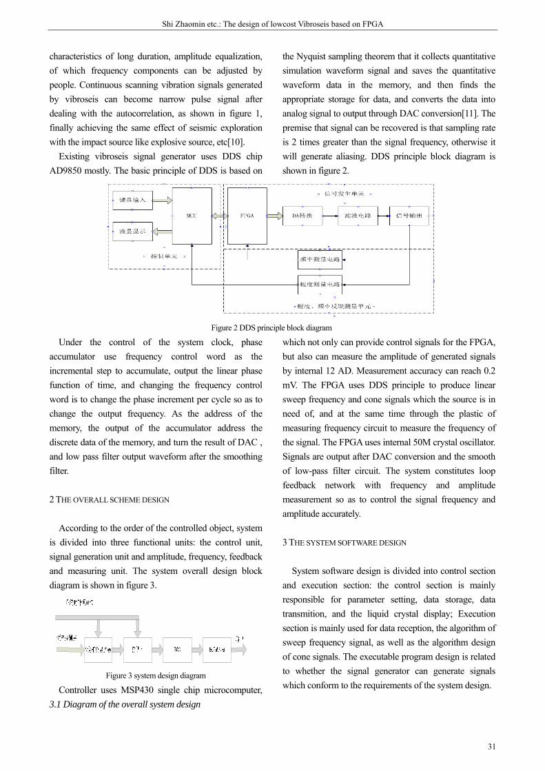
Shi Zhaomin etc.: The design of lowcost Vibroseis based on FPGA
31
characteristics of long duration, amplitude equalization, of which frequency components can be adjusted by people. Continuous scanning vibration signals generated by vibroseis can become narrow pulse signal after dealing with the autocorrelation, as shown in figure 1, finally achieving the same effect of seismic exploration with the impact source like explosive source, etc[10].
Existing vibroseis signal generator uses DDS chip AD9850 mostly. The basic principle of DDS is based on
the Nyquist sampling theorem that it collects quantitative simulation waveform signal and saves the quantitative waveform data in the memory, and then finds the appropriate storage for data, and converts the data into analog signal to output through DAC conversion[11]. The premise that signal can be recovered is that sampling rate is 2 times greater than the signal frequency, otherwise it will generate aliasing. DDS principle block diagram is shown in figure 2.
Figure 2 DDS principle block diagram
Under the control of the system clock, phase accumulator use frequency control word as the incremental step to accumulate, output the linear phase function of time, and changing the frequency control word is to change the phase increment per cycle so as to change the output frequency. As the address of the memory, the output of the accumulator address the discrete data of the memory, and turn the result of DAC , and low pass filter output waveform after the smoothing filter.
2 THE OVERALL SCHEME DESIGN
According to the order of the controlled object, system is divided into three functional units: the control unit, signal generation unit and amplitude, frequency, feedback and measuring unit. The system overall design block diagram is shown in figure 3.
Figure 3 system design diagram
Controller uses MSP430 single chip microcomputer,
which not only can provide control signals for the FPGA, but also can measure the amplitude of generated signals by internal 12 AD. Measurement accuracy can reach 0.2 mV. The FPGA uses DDS principle to produce linear sweep frequency and cone signals which the source is in need of, and at the same time through the plastic of measuring frequency circuit to measure the frequency of the signal. The FPGA uses internal 50M crystal oscillator. Signals are output after DAC conversion and the smooth of low-pass filter circuit. The system constitutes loop feedback network with frequency and amplitude measurement so as to control the signal frequency and amplitude accurately.
3 THE SYSTEM SOFTWARE DESIGN
System software design is divided into control section and execution section: the control section is mainly responsible for parameter setting, data storage, data transmition, and the liquid crystal display; Execution section is mainly used for data reception, the algorithm of sweep frequency signal, as well as the algorithm design of cone signals. The executable program design is related to whether the signal generator can generate signals which conform to the requirements of the system design.
3.1 Diagram of the overall system design
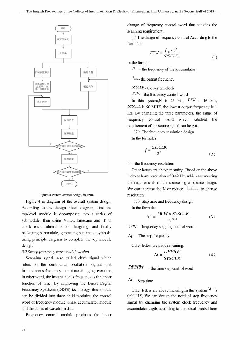
期 The English Proceedings of the College of Instrumentation & Electrical Engineering, Jilin University, in the Second Half of 2013
32
Figure 4 system overall design diagram
Figure 4 is diagram of the overall system design. According to the design block diagram, first the top-level module is decomposed into a series of submodule, then using VHDL language and IP to check each submodule for designing, and finally packaging submodule, generating schematic symbols, using principle diagram to complete the top module design. 3.2 Sweep frequency wave module design
Scanning signal, also called chirp signal which refers to the continuous oscillation signals that instantaneous frequency monotone changing over time, in other word, the instantaneous frequency is the linear function of time. By improving the Direct Digital Frequency Synthesis (DDFS) technology, this module can be divided into three child modules: the control word of frequency module, phase accumulator module and the tables of waveform data.
Frequency control module produces the linear
change of frequency control word that satisfies the scanning requirement.
(1) The design of frequency control According to the formula:
out 2NfFTWSYSCLK
×=
(1) In the formula
N -- the frequency of the accumulator
outf -- the output frequency
SYSCLK - the system clock FTW - the frequency control word In this system,N is 26 bits, FTW is 16 bits,
SYSCLK is 50 MHZ, the lowest output frequency is 1 Hz. By changing the three parameters, the range of frequency control word which satisfied the requirement of the source signal can be got. (2)The frequency resolution design In the formula:
2N
SYSCLKf = (2)
f— the frequency resolution Other letters are above meaning ,Based on the above
indexes have resolution of 0.49 Hz, which are meeting the requirements of the source signal source design. We can increase the N or reduce to change resolution. (3)Step time and frequency design In the formula:
12N
DFW SYSCLKf −
×Δ = (3)
DFW— frequency stepping control word
fΔ —The step frequency
Other letters are above meaning. DFFRWtSYSCLK
Δ = (4)
DFFRW— the time step control word
tΔ —Step time
Other letters are above meaning.In this system fΔ is 0.99 HZ, We can design the need of step frequency signal by changing the system clock frequency and accumulator digits according to the actual needs.There
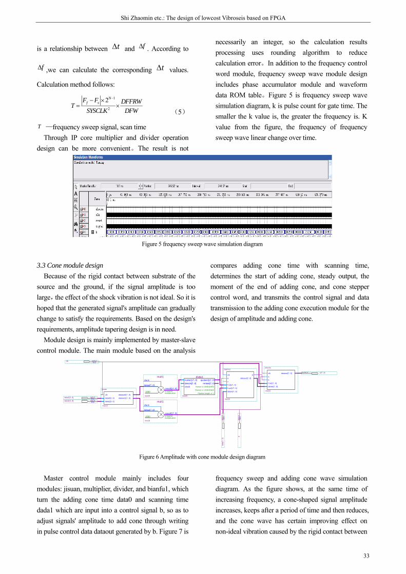
Shi Zhaomin etc.: The design of lowcost Vibroseis based on FPGA
33
is a relationship between tΔ and fΔ . According to
fΔ ,we can calculate the corresponding tΔ values.
Calculation method follows:
1
2
2Nf sF F DFFRWTSYSCLK DFW
−− ×= ×
(5)
T —frequency sweep signal, scan time Through IP core multiplier and divider operation
design can be more convenient。The result is not
necessarily an integer, so the calculation results processing uses rounding algorithm to reduce calculation error。In addition to the frequency control word module, frequency sweep wave module design includes phase accumulator module and waveform data ROM table。Figure 5 is frequency sweep wave simulation diagram, k is pulse count for gate time. The smaller the k value is, the greater the frequency is. K value from the figure, the frequency of frequency sweep wave linear change over time.
Figure 5 frequency sweep wave simulation diagram
3.3 Cone module design
Because of the rigid contact between substrate of the source and the ground, if the signal amplitude is too large,the effect of the shock vibration is not ideal. So it is hoped that the generated signal's amplitude can gradually change to satisfy the requirements. Based on the design's requirements, amplitude tapering design is in need.
Module design is mainly implemented by master-slave control module. The main module based on the analysis
compares adding cone time with scanning time, determines the start of adding cone, steady output, the moment of the end of adding cone, and cone stepper control word, and transmits the control signal and data transmission to the adding cone execution module for the design of amplitude and adding cone.
o[7..0]OUTPUT
1000 Unsignedmultiplication
dataa[7..0]
clock
result[17..0]
mult1
inst16
1000 Unsignedmultiplication
dataa[7..0]
clock
result[17..0]
mult1
inst18
Pipeline length of 1
Denom is UNSIGNED
Numer is UNSIGNED
numer[17..0]denom[7..0]clock
quotient[17..0]remain[7..0]
divde1
inst20
clk
a
b
f cw[17..0]
datain[7..0]
dataout[7..0]
shuchu
inst22
clk
data0[3..0]
data1[3..0]
dataout0[7..0]
dataout1[7..0]
jisuan
inst15
clk
a
c
f cw[17..0]
f cw1[17..0]
datain[7..0]
b
dataout[7..0]
bianf u1
inst23
VCC
dIN
PUT
VCC
data
[7..0
]IN
PUT
VCCclk INPUT
VCCdata0[3..0] INPUT
VCCdata1[3..0] INPUT
Figure 6 Amplitude with cone module design diagram
Master control module mainly includes four
modules: jisuan, multiplier, divider, and bianfu1, which turn the adding cone time data0 and scanning time dada1 which are input into a control signal b, so as to adjust signals' amplitude to add cone through writing in pulse control data dataout generated by b. Figure 7 is
frequency sweep and adding cone wave simulation diagram. As the figure shows, at the same time of increasing frequency, a cone-shaped signal amplitude increases, keeps after a period of time and then reduces, and the cone wave has certain improving effect on non-ideal vibration caused by the rigid contact between
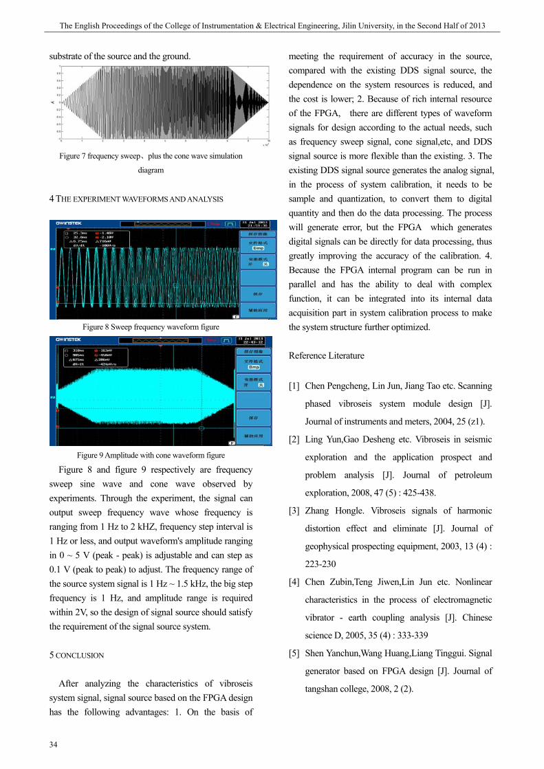
期 The English Proceedings of the College of Instrumentation & Electrical Engineering, Jilin University, in the Second Half of 2013
34
substrate of the source and the ground.
Figure 7 frequency sweep、plus the cone wave simulation
diagram
4 THE EXPERIMENT WAVEFORMS AND ANALYSIS
Figure 8 Sweep frequency waveform figure
Figure 9 Amplitude with cone waveform figure
Figure 8 and figure 9 respectively are frequency sweep sine wave and cone wave observed by experiments. Through the experiment, the signal can output sweep frequency wave whose frequency is ranging from 1 Hz to 2 kHZ, frequency step interval is 1 Hz or less, and output waveform's amplitude ranging in 0 ~ 5 V (peak - peak) is adjustable and can step as 0.1 V (peak to peak) to adjust. The frequency range of the source system signal is 1 Hz ~ 1.5 kHz, the big step frequency is 1 Hz, and amplitude range is required within 2V, so the design of signal source should satisfy the requirement of the signal source system.
5 CONCLUSION
After analyzing the characteristics of vibroseis system signal, signal source based on the FPGA design has the following advantages: 1. On the basis of
meeting the requirement of accuracy in the source, compared with the existing DDS signal source, the dependence on the system resources is reduced, and the cost is lower; 2. Because of rich internal resource of the FPGA, there are different types of waveform signals for design according to the actual needs, such as frequency sweep signal, cone signal,etc, and DDS signal source is more flexible than the existing. 3. The existing DDS signal source generates the analog signal, in the process of system calibration, it needs to be sample and quantization, to convert them to digital quantity and then do the data processing. The process will generate error, but the FPGA which generates digital signals can be directly for data processing, thus greatly improving the accuracy of the calibration. 4. Because the FPGA internal program can be run in parallel and has the ability to deal with complex function, it can be integrated into its internal data acquisition part in system calibration process to make the system structure further optimized.
Reference Literature
[1] Chen Pengcheng, Lin Jun, Jiang Tao etc. Scanning
phased vibroseis system module design [J].
Journal of instruments and meters, 2004, 25 (z1).
[2] Ling Yun,Gao Desheng etc. Vibroseis in seismic
exploration and the application prospect and
problem analysis [J]. Journal of petroleum
exploration, 2008, 47 (5) : 425-438.
[3] Zhang Hongle. Vibroseis signals of harmonic
distortion effect and eliminate [J]. Journal of
geophysical prospecting equipment, 2003, 13 (4) :
223-230
[4] Chen Zubin,Teng Jiwen,Lin Jun etc. Nonlinear
characteristics in the process of electromagnetic
vibrator - earth coupling analysis [J]. Chinese
science D, 2005, 35 (4) : 333-339
[5] Shen Yanchun,Wang Huang,Liang Tinggui. Signal
generator based on FPGA design [J]. Journal of
tangshan college, 2008, 2 (2).
Shi Zhaomin etc.: The design of lowcost Vibroseis based on FPGA
35
[6] Miller R D, Pullan S E, Waldner J S, et al. Field
comparison of shallow seismic sources[J].
Geophysics, 1986, 51(11): 2067-2092.
[7] Lin Jun. The principle and application of
electromagnetic drive vibroseis seismic
prospecting [M]. Science press, 2004
[8] Jiang Tao,Lin Jun,Li Tonglin etc. The study of
phased source to improve the SNR of seismic
signal [J]. Journal of geophysics, 2006, 49 (6) :
1819-1825.
[9] Jiang Tao,Lin Jun,Yang Dong etc. Phased source
directional seismic signal analysis [J]. Journal of
geophysics, 2008, 51 (5) : 1551-1556.
[10] Lin Jun,Chen Pengcheng,Jiang Tao,Chen Zubin.
Shallow seismic exploration of vibroseis signal
design. Progress in geophysics, 2004, 12 (4) : 807
~ 811.
[11] Gao Shiyou,Hu Xueshen,Du Xingli etc. The
design of DDS signal generator based on FPGA
[J]. Journal of modern electronic technology, 2009,
32 (16) : 35 to 37.
期 The English Proceedings of the College of Instrumentation & Electrical Engineering, Jilin University, in the Second Half of 2013
36
Design of Gravitational Acceleration Measuring Device Based on Balance Method
Qian Chenghui, Chen Changsong
(College of Instrumentation and Electrical Engineering,Jilin University,Changchun 130026,China) Abstract—Gravitational acceleration is of great significance in scientific research and social production.There are several methods
measuring gravitational acceleration,such as free-fall method, air-cushion guide method, pendulum method,balance method , etc.
Devices based on these methods are large and imprecise. In this paper,the method is improved from traditional balance method and
the arithmetic is based on Newton’s second and third law.The device figures out the local gravitational acceleration using a cube
made up of 6 piezoresistive transducers when the quality of nonmagnetic iron ball and the force on it are kown.The precision of this
device reaches ±0.002m*s-2and the relative error is lower than 0.043%,which applies to teaching and scientific research.
Key words—gravitational acceleration; balance method; piezoresistive transducer; nonmagnetic iron ball
GRAVITATIONAL acceleration is an important physical quantity, whether in the physical laboratory or in scientific research and applications, measuring gravitational acceleration is of great significance [1].
At present, in the field of the gravitational acceleration measurement, the methods of air track and Doppler effects is the more advanced ones. Now, our country has greater breakthrough in this field, gravitational acceleration measurement to the outside world step by step [2].Technology level and research depth is steadily rising in field of research。
Common method of measuring gravitational acceleration are: the free-fall method, the simple pendulum method, slope method, balance method and dripping method[3], etc. The accuracy of traditional measurement is not high and of the device volume is clumsy. Traditional balance method, respectively, figures out mass(m) and weight(G) of object with the balance theory and gravity acceleration g = G/m can be obtained. Due to the accuracy of the traditional spring dynamometer is inaccurate, which causes the gravity measurement error [4]. And in the artificial measurement, many factors such as artificial record can lead to inaccurate data.
Based on balanced method using piezoresistive sensor, the gravitational acceleration measurement works using hexahedron type pressure acquisition device,which overcome the problem in traditional measure that when the single side is forced,the device must maintain absolute level of defects.Then after signal adjusting and conversion by the A/D,the deivce collects resultant force
value.For hexahedron is a kingd of symmetrical graph, the size of the plane stress theory have symmetry and rotary substitution, the amount of calculation and complexity of algorithm are reduces.Finally, the controller calculates the local gravitational acceleration value according to the mass quality of the object.
1 DESIGN SCHEME AND ALGORITHM ANALYSIS
1.1 Design Scheme Gravitational acceleration measurement device was
improved basing on the traditional balance method.Put a nonmagnetic iron in hollow regular hexahedron composed of six pieces of piezoresistive sensors,so six bearing surfaces form the six channels.data acquisition system principle block diagram is shown in figure 1:
Figure1. Principle Block of System
Pressure sensor using piezoresistive pressure sensor [5-6], its main principle is based on the piezoresistive effect, namely the resistivity of solid materials will changes under the action of stress. So when the feeling part of the sensor component (semiconductor materials) is under deformation of stress, the internal resistance of

Chen Changsong etc.: Design of Gravitational Acceleration Measuring Device Based on Balance Method
37
the circuit connected to the sensor will produce corresponding change, which changes the output voltage value. Six pressure sensor output voltage value through filtering and six channels of A/D transformed from regular hexahedron system to collect various surface by pressure value.And according to the resultant standards and Newton's second and third law the gravitational acceleration in regional systems can be calculated.
According to the balance method in classical physics [7], analysing the system including regular hexahedron and non-magnetic steel ball ,it shows that when the system balance,there are at least one side forced, up to three sides are forced in the regular hexahedron, and they are vertical to the adjacent ones, as shown in figure 2:
(a)Force on One Surface (b)Force on Two Surface
(c)Force on Three Surface
Figure 2. Stress Analysis of Different Situation
In the the figure, F1, F2, F3 are the support from hexahedron to the nonmagnetic iron ball on the certain face ,and G stands for gravity of the nonmagnetic iron ball. 1.2 Algorithm Analysis
F1, F2, F3, F4, F5 and F6 are supports from regular hexahedron to nonmagnetic iron ball, as shown in figure in figure 3:
Figure3. Stress Analysis of System
In regular hexahedron, adjacent surfaces are vertical and opposite surfaces keep parallel. According to synthetic criterion, when the system are balanced,the resultant support produced by the surfaces turns out:
2 2 24 1 5 2 6 3( - ) +( - ) +( - )F F F F F F F= ⑴
When force on one surface shown in figure2(a):
2 3 4 5 6= 0F F F F F= = = = ⑵
Conclude by (1)(2):
1F F= ⑶
When force on two surface shown in figure2(a):
3 4 5 6 0F F F F= = = = ⑷
Conclude by (1)(4):
2 21 2+F F F=
⑸ When force on three surface shown in figure2(a):
4 5 6 0F F F= = = ⑹
Conclude by (1)(6):
2 2 21 2 3+ +F F F F=
⑺ Because this system is composed of symmetrical
objects, such as sphere, cube, the above algorithm meet the symmetry and rotary substitution sex, namely regular hexahedron any one, two or three adjacent surfaces stress distribution are all meet the above formula.
Analys the system when it is balanced and according to the Newton's third law: Action and reaction between two objects,are in the same line, equal and in the opposite direction [8];While balance force are two forces acting on the same object and of the same value, direction, and also in a straight line. Therefore,pressure on each surface of regular hexahedron pressured by nonmagnetic iron ball and its corresponding support is a pair of action and reaction, and they are of the same value and reverse; And resultant support from regular hexahedron to nonmagnetic iron ball nonmagnetic iron ball’s gravity are a pair of balance force, and they are also of the same value and reverse.
| | | |G F=ur ur
⑻
According to Newton's second law: the acceleration of the object is directly proportional to the force of the object and is inversely proportional to the quality of the
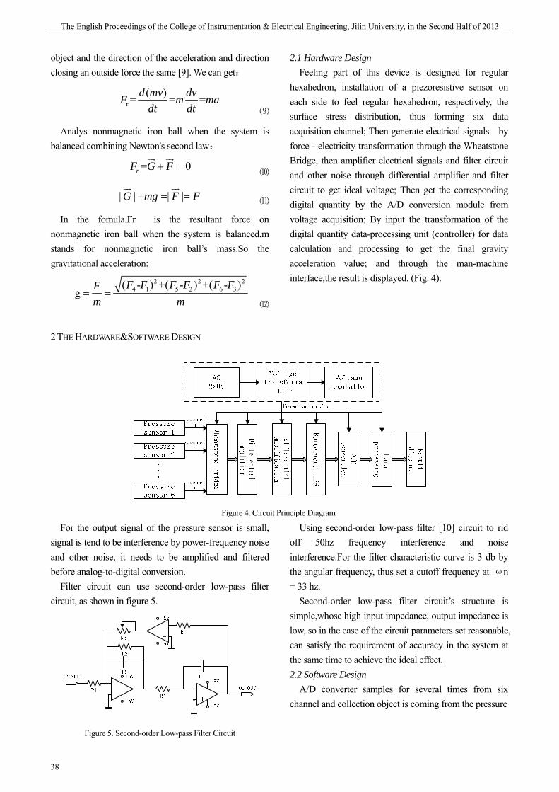
期 The English Proceedings of the College of Instrumentation & Electrical Engineering, Jilin University, in the Second Half of 2013
38
object and the direction of the acceleration and direction closing an outside force the same [9]. We can get:
r( )= = =d mv dvF m madt dt ⑼
Analys nonmagnetic iron ball when the system is balanced combining Newton's second law:
= 0rF G F+ =ur ur
⑽
| | = | |G mg F F= =ur ur
⑾
In the fomula,Fr is the resultant force on nonmagnetic iron ball when the system is balanced.m stands for nonmagnetic iron ball’s mass.So the gravitational acceleration:
2 2 24 1 5 2 6 3( - ) +( - ) +( - )
gF F F F F FF
m m= =
⑿
2 THE HARDWARE&SOFTWARE DESIGN
2.1 Hardware Design Feeling part of this device is designed for regular
hexahedron, installation of a piezoresistive sensor on each side to feel regular hexahedron, respectively, the surface stress distribution, thus forming six data acquisition channel; Then generate electrical signals by force - electricity transformation through the Wheatstone Bridge, then amplifier electrical signals and filter circuit and other noise through differential amplifier and filter circuit to get ideal voltage; Then get the corresponding digital quantity by the A/D conversion module from voltage acquisition; By input the transformation of the digital quantity data-processing unit (controller) for data calculation and processing to get the final gravity acceleration value; and through the man-machine interface,the result is displayed. (Fig. 4).
Figure 4. Circuit Principle Diagram
For the output signal of the pressure sensor is small, signal is tend to be interference by power-frequency noise and other noise, it needs to be amplified and filtered before analog-to-digital conversion.
Filter circuit can use second-order low-pass filter circuit, as shown in figure 5.
Figure 5. Second-order Low-pass Filter Circuit
Using second-order low-pass filter [10] circuit to rid off 50hz frequency interference and noise interference.For the filter characteristic curve is 3 db by the angular frequency, thus set a cutoff frequency at ωn = 33 hz.
Second-order low-pass filter circuit’s structure is simple,whose high input impedance, output impedance is low, so in the case of the circuit parameters set reasonable, can satisfy the requirement of accuracy in the system at the same time to achieve the ideal effect. 2.2 Software Design
A/D converter samples for several times from six channel and collection object is coming from the pressure
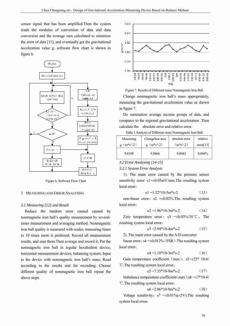
Chen Changsong etc.: Design of Gravitational Acceleration Measuring Device Based on Balance Method
39
sensor signal that has been amplified.Then the system reads the modulus of conversion of data and data conversion and the average sum calculated to minimize the error of data [11], and eventually get the gravitational acceleration value g, software flow chart is shown in figure 6.
Figure 6. Software Flow Chart
3 MEASURING AND ERROR ANALYSING
3.1 Measuring [12] and Result Reduce the random error caused caused by
nonmagnetic iron ball’s quality measurement by several- times measurement and averaging method. Nonmagnetic iron ball quality is measured with scales, measuring times to 10 times more is preferred; Record all measurement results, and sum them.Then average and record it; Put the nonmagnetic iron ball in regular hexahedron device, horizontal measurement devices, balancing system; Input to the device with nonmagnetic iron ball’s mass; Read according to the results and for recording; Choose different quality of nonmagnetic iron ball repeat the above steps.
Figure 7. Results of Different-mass Nonmagnetic Iron Ball
Change nonmagnetic iron ball’s mass appropriately, measuring the gravitational acceleration value as shown in figure 7.
Do summation average income groups of data, and compares to the regional gravitational acceleration .Then calculate the absolute error and relative error.
Table 1 Analysis of Different-mass Nonmagnetic Iron Ball
Measuring
g(m*s^-2)
Changchun area
g(m*s^-2)
absolute error
(m*s^-2)
relative
error[13]
9.8109 9.8066 0.0043 0.044%
3.2 Error Analysing [14-15] 3.2.1 System Error Analysis
1). The main error caused by the pressure sensor sensitivity error: s1=±0.05mV/mm.The resulting system local error:
e1 =1.22*10-5m*s-2 (13) non-linear error:s2 =±0.02%.The resulting system
local error: e2 =1.96*10-3m*s-2 (14)
Zero temperature error: s3 =±0.03%/10,The resulting system local error:
e3 =2.94*10-4m*s-2 (15) 2). The main error caused by the A/D converter linear error:s4 =±0.012%(FSR).The resulting system
local error: e4 =1.18*10-3m*s-2 (16)
Gain temperature coefficient(max):s5=±25* 10-6/.The resulting system local error:
e5 =7.35*10-9m*s-2 (17) Imbalance temperature coefficient(max):s6 =±7*10-6/
.The resulting system local error: e6 =2.06*10-9m*s-2 (18)
Voltage sensitivity:s7 =±0.01%(±5V).The resulting system local error:

期 The English Proceedings of the College of Instrumentation & Electrical Engineering, Jilin University, in the Second Half of 2013
40
e7 =2.44*10-8m*s-2 (19) 3). Error caused by environment temperature change Due to the different material of parts in the module of
devices,which has intrinsic to the thermal expansion coefficient of various materials.When system is working, the environment temperature changes, will produce relative displacement between components, local error caused by temperature. Device’s using request the environment temperature change Δ t < 2 , the temperature error of local error caused by the system:
e8 =1.24*10-5m*s-2 (20) According to the uncertain system error formula,the
total system error synthesis:
8 82 -3 2
1 1
| | =2.31*10 m*i ii i
e e e s−= =
Δ =∑ ∑或 (21)
3.2.2 Random error analysis 1). Random error caused by angle between surface and
surface :
2 2 2 21 1 2 1 2 1 2= 2 cosr F F F F F Fθ+ − − +
(22) The resulting random local error:
Δ1=1.64*10-3m*s-2 (23) 2). Measurement error caused by nonmagnetic iron
ball’s mass: 2 0.01gr = ±
When nonmagnetic iron ball’s mass g>10g, the resulting random local error:
Δ2(max)=9.78*10-4m*s-2 (24) Total synthesis of random error, based on the principles
of action:
23 2
1
1.91*10 *ii
m s− −
=
Δ = Δ =∑ ∑ (25)
In conclusion, the overall error: 8
3 2
1
| | (2.31+1.91)*10 *m*sii
e e − −
=
= +Δ =∑∑(26)
Gravitational acceleration in Changchun area: g0= 9.8066m*s-2, overall relative error:
0
0 0
| | =0.043e ggSg g
−Δ= = %
(27)
4 CONCLUSION
Improved from the traditional balance method in order
to, put forward regular hexahedron mechanical synthesis method and multi-channel data acquisition. Data transformation and processing of regular hexahedron different loading cases to figure out gravitational acceleration value, in order to realize miniaturization, intelligent and high precision of the Gravitational Acceleration measuring device.
The precision of the measuring device is + / - 0.002 m * s-2,and the relative error less than 0.043%,which can be applied in the experiment teaching and scientific research.In the same time, provides a new reference direction for the design and improvement of the gravitational acceleration measuring device.
REFERENCES CITED
[1] Ying,F.B., The Surface of The Earth Acceleration of
Gravity Anomaly and Application [J]. Physics
Teaching to Discuss,2010,28(12):53-54.
[2] Lu,J.S., To The Outside World the Gravitational
Acceleration Measurement in Our Country [J].China
Metrology,1997; 1:36—37.
[3] Han,D.A,Zeng,Y.G.,Chen,X.L., The Acceleration of
Gravity Measurement System Based on Labview [J].
Laboratory Research and Exploration, 2007, 26
(11) :33-35.
[4] Han,Z.X.,Xu,Y.,Gan,Z.Q., Using The Doppler Effect
Measuring Acceleration of Gravity [M] .
Measurement and Testing Technology, 2009,36
(8):32-33
[5] Ji,C.Q,Li,Y.Q., Silicon Force Sensor Measuring The
Liquid Surface Tension Coefficient and Liquid
Membrane Stress Analysis [J]. Experimental
Technology and Management,2011,28(4):46-48.
[6] Teng,J.C.,Chen,C.P.,Guo,H., Adjustment of
Piezoresistive Pressure Sensor Signal [J]. Instrument
Technique and Sensor,2009(10):360-362.
[7] Wang,M., Load Balancing Method of Theoretical
Analysis and Applications [J]. Traffic
World,2007(5):113-114.

Chen Changsong etc.: Design of Gravitational Acceleration Measuring Device Based on Balance Method
41
[8] Dai,C.Q., The Newton's third law practice [J].
Technology and Physics Teaching,2005,13(4):42-43.
[9] Liu,J.F.,Luo,X.K., Verify Newton's Second law
Experiment Force Measurement Methods Were
Reviewed [J].Experiment Teaching and
Instrument,1998(2):7-9.
[10] Kang,G.H., fundamentals of electronic technology
[M]. Beijing: Higher Education
Press,2011(11):418-423.
[11] Lu,Z.H.,The Application of SCM in The Design of
Physical Experiment [J], college physics
experiment,2001,4(14):56—57.
[12] Zhou,Y.H.,Xu,D.S., Acceleration of Gravity
Measurement and Correct Calculation [M] . college
physics experiment,2002(6):18-24.
[13] Lin,Z.J., Electronic Measurement Techniques
[M].Beijing: Electronic Industry
Press,2011(11):12-15.
[14] Cheng,D.F. , Lin,J., Intelligent Instrument
[M].Beijing: Mechanical Industry Press,2012(7):
42-55.
[15] Wu,X.H., Sensor and Signal Processing [M].Beijing:
Electronic Industry Press,1998:1-14.
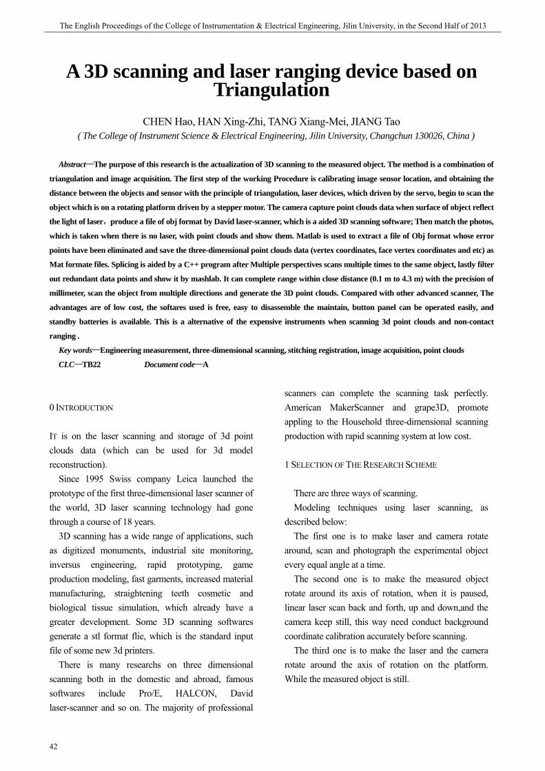
期 The English Proceedings of the College of Instrumentation & Electrical Engineering, Jilin University, in the Second Half of 2013
42
A 3D scanning and laser ranging device based on Triangulation
CHEN Hao, HAN Xing-Zhi, TANG Xiang-Mei, JIANG Tao
( The College of Instrument Science & Electrical Engineering, Jilin University, Changchun 130026, China ) Abstract—The purpose of this research is the actualization of 3D scanning to the measured object. The method is a combination of
triangulation and image acquisition. The first step of the working Procedure is calibrating image sensor location, and obtaining the
distance between the objects and sensor with the principle of triangulation, laser devices, which driven by the servo, begin to scan the
object which is on a rotating platform driven by a stepper motor. The camera capture point clouds data when surface of object reflect
the light of laser,produce a file of obj format by David laser-scanner, which is a aided 3D scanning software; Then match the photos,
which is taken when there is no laser, with point clouds and show them. Matlab is used to extract a file of Obj format whose error
points have been eliminated and save the three-dimensional point clouds data (vertex coordinates, face vertex coordinates and etc) as
Mat formate files. Splicing is aided by a C++ program after Multiple perspectives scans multiple times to the same object, lastly filter
out redundant data points and show it by mashlab. It can complete range within close distance (0.1 m to 4.3 m) with the precision of
millimeter, scan the object from multiple directions and generate the 3D point clouds. Compared with other advanced scanner, The
advantages are of low cost, the softares used is free, easy to disassemble the maintain, button panel can be operated easily, and
standby batteries is available. This is a alternative of the expensive instruments when scanning 3d point clouds and non-contact
ranging .
Key words—Engineering measurement, three-dimensional scanning, stitching registration, image acquisition, point clouds
CLC—TB22 Document code—A
0 INTRODUCTION
IT is on the laser scanning and storage of 3d point clouds data (which can be used for 3d model reconstruction).
Since 1995 Swiss company Leica launched the prototype of the first three-dimensional laser scanner of the world, 3D laser scanning technology had gone through a course of 18 years.
3D scanning has a wide range of applications, such as digitized monuments, industrial site monitoring, inversus engineering, rapid prototyping, game production modeling, fast garments, increased material manufacturing, straightening teeth cosmetic and biological tissue simulation, which already have a greater development. Some 3D scanning softwares generate a stl format flie, which is the standard input file of some new 3d printers.
There is many researchs on three dimensional scanning both in the domestic and abroad, famous softwares include Pro/E, HALCON, David laser-scanner and so on. The majority of professional
scanners can complete the scanning task perfectly. American MakerScanner and grape3D, promote appling to the Household three-dimensional scanning production with rapid scanning system at low cost.
1 SELECTION OF THE RESEARCH SCHEME
There are three ways of scanning. Modeling techniques using laser scanning, as
described below: The first one is to make laser and camera rotate
around, scan and photograph the experimental object every equal angle at a time.
The second one is to make the measured object rotate around its axis of rotation, when it is paused, linear laser scan back and forth, up and down,and the camera keep still, this way need conduct background coordinate calibration accurately before scanning.
The third one is to make the laser and the camera rotate around the axis of rotation on the platform. While the measured object is still.
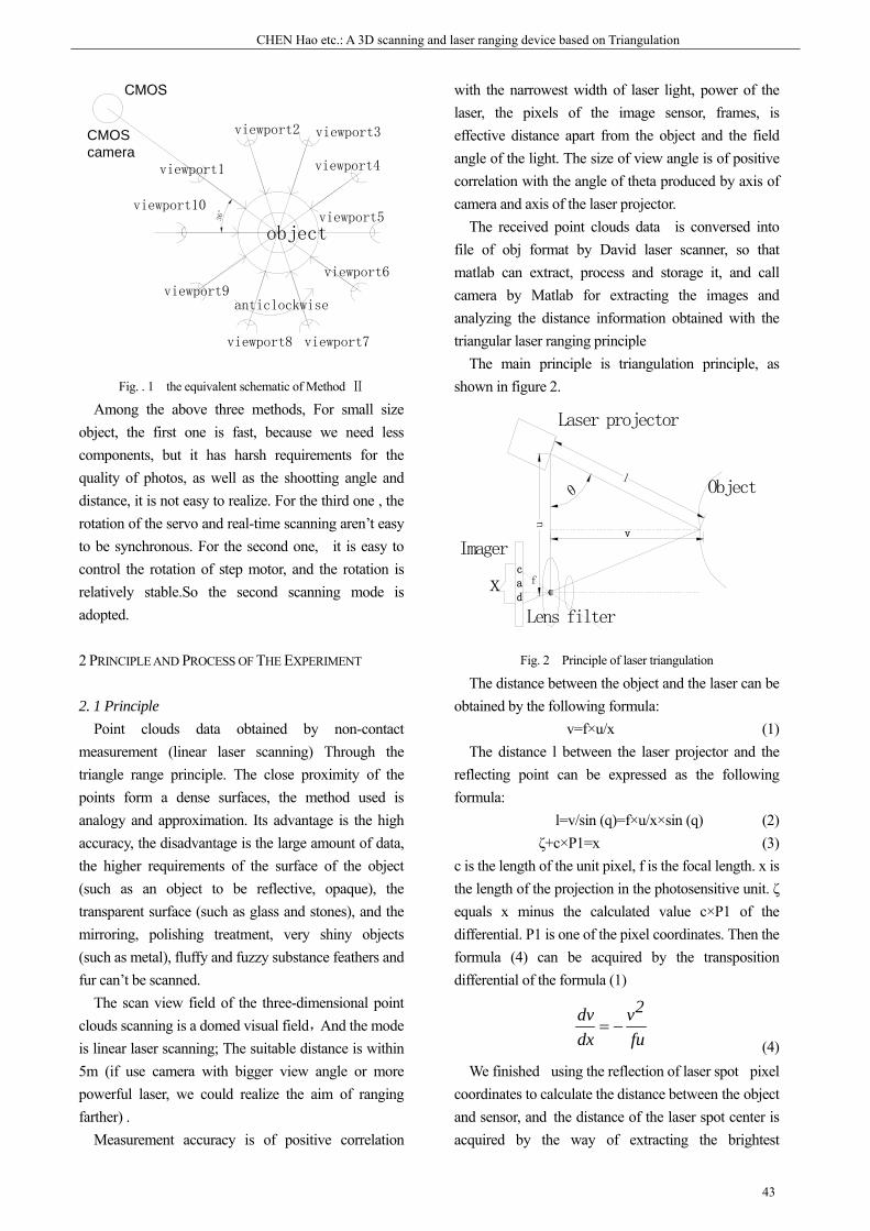
CHEN Hao etc.: A 3D scanning and laser ranging device based on Triangulation
43
object
viewport10
viewport1
viewport2
viewport9
viewport8 viewport7
viewport6
viewport5
viewport4
viewport3
36°
anticlockwise
CMOScamera
Fig. . 1 the equivalent schematic of Method Ⅱ
Among the above three methods, For small size object, the first one is fast, because we need less components, but it has harsh requirements for the quality of photos, as well as the shootting angle and distance, it is not easy to realize. For the third one , the rotation of the servo and real-time scanning aren’t easy to be synchronous. For the second one, it is easy to control the rotation of step motor, and the rotation is relatively stable.So the second scanning mode is adopted.
2 PRINCIPLE AND PROCESS OF THE EXPERIMENT
2. 1 Principle Point clouds data obtained by non-contact
measurement (linear laser scanning) Through the triangle range principle. The close proximity of the points form a dense surfaces, the method used is analogy and approximation. Its advantage is the high accuracy, the disadvantage is the large amount of data, the higher requirements of the surface of the object (such as an object to be reflective, opaque), the transparent surface (such as glass and stones), and the mirroring, polishing treatment, very shiny objects (such as metal), fluffy and fuzzy substance feathers and fur can’t be scanned.
The scan view field of the three-dimensional point clouds scanning is a domed visual field,And the mode is linear laser scanning; The suitable distance is within 5m (if use camera with bigger view angle or more powerful laser, we could realize the aim of ranging farther) .
Measurement accuracy is of positive correlation
with the narrowest width of laser light, power of the laser, the pixels of the image sensor, frames, is effective distance apart from the object and the field angle of the light. The size of view angle is of positive correlation with the angle of theta produced by axis of camera and axis of the laser projector.
The received point clouds data is conversed into file of obj format by David laser scanner, so that matlab can extract, process and storage it, and call camera by Matlab for extracting the images and analyzing the distance information obtained with the triangular laser ranging principle
The main principle is triangulation principle, as shown in figure 2.
u
l
f
Laser projector
v
θ
cad
Lens filter
Object
Imager
x
Fig. 2 Principle of laser triangulation
The distance between the object and the laser can be obtained by the following formula:
v=f×u/x (1) The distance l between the laser projector and the
reflecting point can be expressed as the following formula:
l=v/sin (q)=f×u/x×sin (q) (2) ζ+c×P1=x (3)
c is the length of the unit pixel, f is the focal length. x is the length of the projection in the photosensitive unit. ζ equals x minus the calculated value c×P1 of the differential. P1 is one of the pixel coordinates. Then the formula (4) can be acquired by the transposition differential of the formula (1)
2dv v dx fu
= − (4)
We finished using the reflection of laser spot pixel coordinates to calculate the distance between the object and sensor, and the distance of the laser spot center is acquired by the way of extracting the brightest
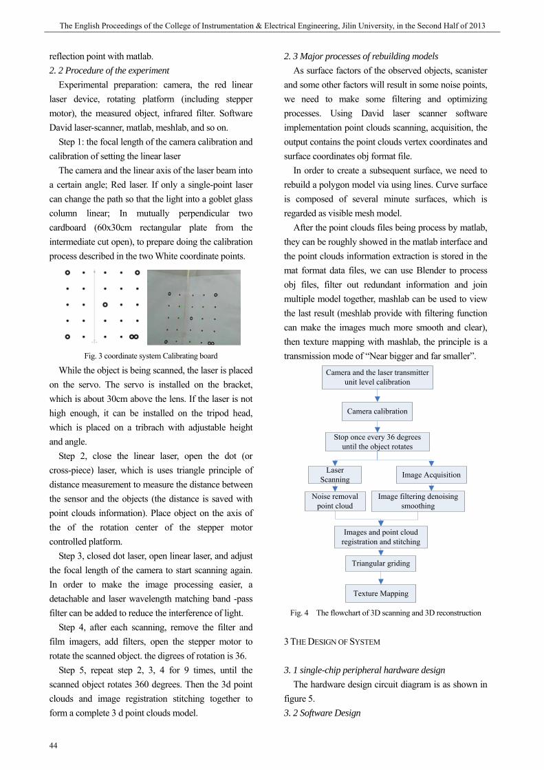
期 The English Proceedings of the College of Instrumentation & Electrical Engineering, Jilin University, in the Second Half of 2013
44
reflection point with matlab. 2. 2 Procedure of the experiment
Experimental preparation: camera, the red linear laser device, rotating platform (including stepper motor), the measured object, infrared filter. Software David laser-scanner, matlab, meshlab, and so on.
Step 1: the focal length of the camera calibration and calibration of setting the linear laser
The camera and the linear axis of the laser beam into a certain angle; Red laser. If only a single-point laser can change the path so that the light into a goblet glass column linear; In mutually perpendicular two cardboard (60x30cm rectangular plate from the intermediate cut open), to prepare doing the calibration process described in the two White coordinate points.
Fig. 3 coordinate system Calibrating board
While the object is being scanned, the laser is placed on the servo. The servo is installed on the bracket, which is about 30cm above the lens. If the laser is not high enough, it can be installed on the tripod head, which is placed on a tribrach with adjustable height and angle.
Step 2, close the linear laser, open the dot (or cross-piece) laser, which is uses triangle principle of distance measurement to measure the distance between the sensor and the objects (the distance is saved with point clouds information). Place object on the axis of the of the rotation center of the stepper motor controlled platform.
Step 3, closed dot laser, open linear laser, and adjust the focal length of the camera to start scanning again. In order to make the image processing easier, a detachable and laser wavelength matching band -pass filter can be added to reduce the interference of light.
Step 4, after each scanning, remove the filter and film imagers, add filters, open the stepper motor to rotate the scanned object. the digrees of rotation is 36.
Step 5, repeat step 2, 3, 4 for 9 times, until the scanned object rotates 360 degrees. Then the 3d point clouds and image registration stitching together to form a complete 3 d point clouds model.
2. 3 Major processes of rebuilding models As surface factors of the observed objects, scanister
and some other factors will result in some noise points, we need to make some filtering and optimizing processes. Using David laser scanner software implementation point clouds scanning, acquisition, the output contains the point clouds vertex coordinates and surface coordinates obj format file.
In order to create a subsequent surface, we need to rebuild a polygon model via using lines. Curve surface is composed of several minute surfaces, which is regarded as visible mesh model.
After the point clouds files being process by matlab, they can be roughly showed in the matlab interface and the point clouds information extraction is stored in the mat format data files, we can use Blender to process obj files, filter out redundant information and join multiple model together, mashlab can be used to view the last result (meshlab provide with filtering function can make the images much more smooth and clear), then texture mapping with mashlab, the principle is a transmission mode of “Near bigger and far smaller”.
Camera and the laser transmitter unit level calibration
Image Acquisition
Stop once every 36 degrees until the object rotates
Noise removal point cloud
Images and point cloud registration and stitching
Laser Scanning
Triangular griding
Image filtering denoising smoothing
Texture Mapping
Camera calibration
Fig. 4 The flowchart of 3D scanning and 3D reconstruction
3 THE DESIGN OF SYSTEM
3. 1 single-chip peripheral hardware design The hardware design circuit diagram is as shown in
figure 5. 3. 2 Software Design
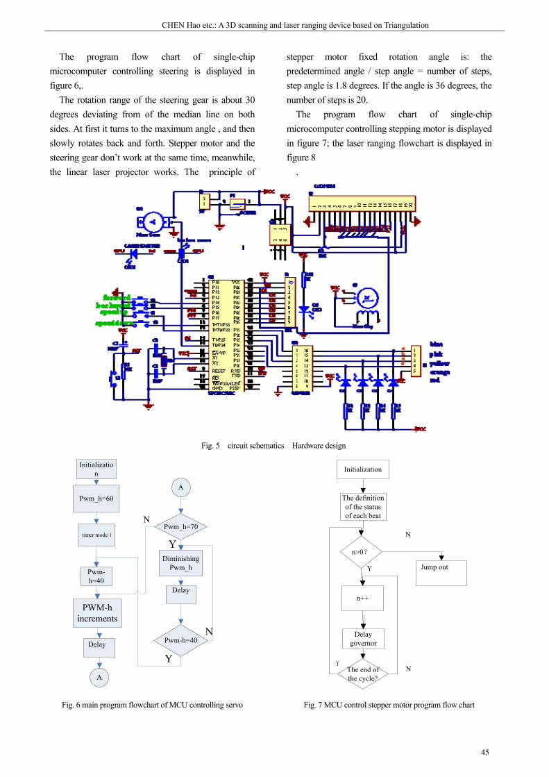
CHEN Hao etc.: A 3D scanning and laser ranging device based on Triangulation
45
The program flow chart of single-chip microcomputer controlling steering is displayed in figure 6,.
The rotation range of the steering gear is about 30 degrees deviating from of the median line on both sides. At first it turns to the maximum angle , and then slowly rotates back and forth. Stepper motor and the steering gear don’t work at the same time, meanwhile, the linear laser projector works. The principle of
stepper motor fixed rotation angle is: the predetermined angle / step angle = number of steps, step angle is 1.8 degrees. If the angle is 36 degrees, the number of steps is 20.
The program flow chart of single-chip microcomputer controlling stepping motor is displayed in figure 7; the laser ranging flowchart is displayed in figure 8
.
Fig. 5 circuit schematics Hardware design
Initialization
timer mode 1
Pwm-h=40
PWM-h increments
Diminishing Pwm_h
Delay
Delay
Pwm_h=60
Pwm_h=70
A
A
Pwm-h=40
Y
N
Y
N
Fig. 6 main program flowchart of MCU controlling servo
The definition of the status of each beat
Initialization
Delay governor
n>0?
Y
N
The end of the cycle?
N
n++
Jump out
Y
Fig. 7 MCU control stepper motor program flow chart
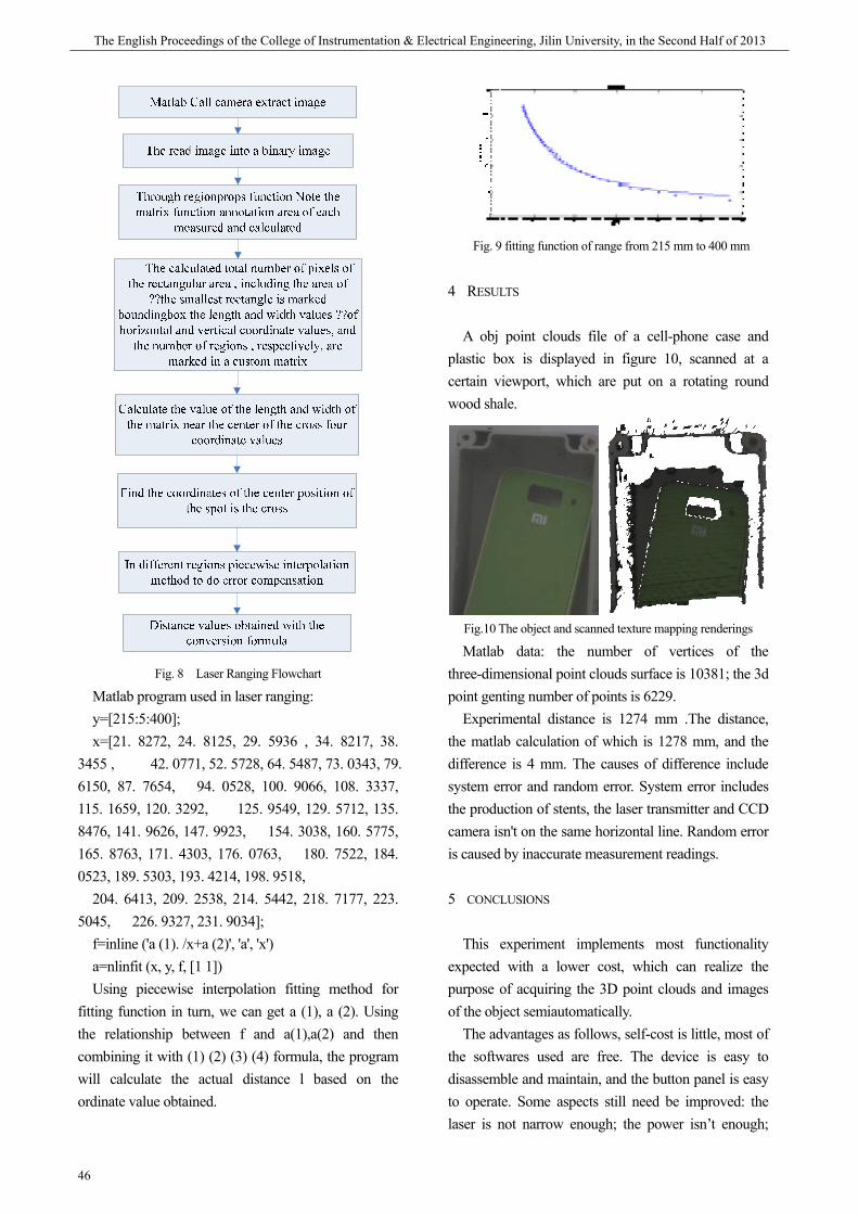
期 The English Proceedings of the College of Instrumentation & Electrical Engineering, Jilin University, in the Second Half of 2013
46
Fig. 8 Laser Ranging Flowchart
Matlab program used in laser ranging: y=[215:5:400]; x=[21. 8272, 24. 8125, 29. 5936 , 34. 8217, 38.
3455 , 42. 0771, 52. 5728, 64. 5487, 73. 0343, 79. 6150, 87. 7654, 94. 0528, 100. 9066, 108. 3337, 115. 1659, 120. 3292, 125. 9549, 129. 5712, 135. 8476, 141. 9626, 147. 9923, 154. 3038, 160. 5775, 165. 8763, 171. 4303, 176. 0763, 180. 7522, 184. 0523, 189. 5303, 193. 4214, 198. 9518,
204. 6413, 209. 2538, 214. 5442, 218. 7177, 223. 5045, 226. 9327, 231. 9034];
f=inline ('a (1). /x+a (2)', 'a', 'x') a=nlinfit (x, y, f, [1 1]) Using piecewise interpolation fitting method for
fitting function in turn, we can get a (1), a (2). Using the relationship between f and a(1),a(2) and then combining it with (1) (2) (3) (4) formula, the program will calculate the actual distance l based on the ordinate value obtained.
Fig. 9 fitting function of range from 215 mm to 400 mm
4 RESULTS
A obj point clouds file of a cell-phone case and plastic box is displayed in figure 10, scanned at a certain viewport, which are put on a rotating round wood shale.
Fig.10 The object and scanned texture mapping renderings
Matlab data: the number of vertices of the three-dimensional point clouds surface is 10381; the 3d point genting number of points is 6229.
Experimental distance is 1274 mm .The distance, the matlab calculation of which is 1278 mm, and the difference is 4 mm. The causes of difference include system error and random error. System error includes the production of stents, the laser transmitter and CCD camera isn't on the same horizontal line. Random error is caused by inaccurate measurement readings.
5 CONCLUSIONS
This experiment implements most functionality expected with a lower cost, which can realize the purpose of acquiring the 3D point clouds and images of the object semiautomatically.
The advantages as follows, self-cost is little, most of the softwares used are free. The device is easy to disassemble and maintain, and the button panel is easy to operate. Some aspects still need be improved: the laser is not narrow enough; the power isn’t enough;

CHEN Hao etc.: A 3D scanning and laser ranging device based on Triangulation
47
pixels of the imager sensor are 640×480; shootting speed is unstable. Therefore, the accuracy is not high. Because the components used are entry-level, it is not very stable, and quality of real-time feature still need to be improved. However, the hardware, software design isn’t very mature, so it can ‘t be put into application temporarily.
References
[1] Nong Jun-bin; triangular mesh generation
algorithms, a LIDAR point clouds Red River [J] ,
2011, 05:170-172
[2] Li tian-Lan, 3D point clouds data processing and
application of [D], Kunming Polytechnic
University , 2011:1 of-33
[3] Xu Gang. forward to establish a 3d model [M] by
the two-dimensional images. Zheng Shun-Yi ,
translated Wuhan: Wuhan University Press, 2006.
[4] Wei Hua, Fu Yong-gang, Zhang Xi-wen drawn
based on the image of the point clouds modeling
its realism, Computer Engineering and Application
(J) , 2010, 20:4-8
[5] Three-dimensional laser scanner hardware design
and implementation[J], SUN Silver, Li Zhong, Ke
Yao-Sen, microcompute development[J] , 1995,
01:11-13
[6] James C. Savage, J. Kevin ONeal, Robert A.
Brown, Powered Low Cost Autonomous Attack
System: coopera-tive, autonomous, wide- area-
search munitions with capability to serve as non-
traditional ISR assets in a network-centric
environment [J]. SPIE, 2005, 5791: 61- 69.
[7] Robert Hauge. LADAR puts the puzzle together
[J]. Spies oemagazine. 2003, (4):18-22
[8] Stamos, P. E. Allen. 3-D model construction using
range and image data[C]. Hilton Head Island:
IEEE Conference on Computer Vision and Pattern
Recognition, 2000, ( 1) : 531536
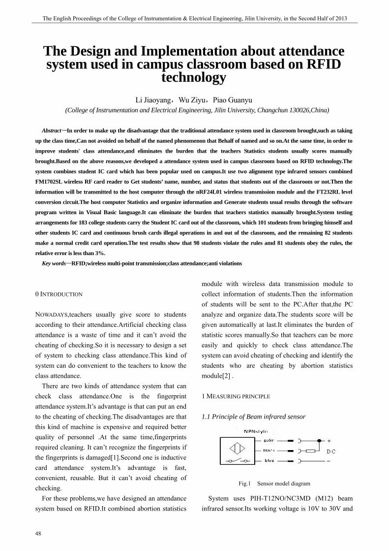
期 The English Proceedings of the College of Instrumentation & Electrical Engineering, Jilin University, in the Second Half of 2013
48
The Design and Implementation about attendance system used in campus classroom based on RFID
technology
Li Jiaoyang,Wu Ziyu,Piao Guanyu (College of Instrumentation and Electrical Engineering, Jilin University, Changchun 130026,China)
Abstract—In order to make up the disadvantage that the traditional attendance system used in classroom brought,such as taking
up the class time,Can not avoided on behalf of the named phenomenon that Behalf of named and so on.At the same time, in order to
improve students' class attendance,and eliminates the burden that the teachers Statistics students usually scores manually
brought.Based on the above reasons,we developed a attendance system used in campus classroom based on RFID technology.The
system combines student IC card which has been popular used on campus.It use two alignment type infrared sensors combined
FM1702SL wireless RF card reader to Get students’ name, number, and status that students out of the classroom or not.Then the
information will be transmitted to the host computer through the nRF24L01 wireless transmission module and the FT232RL level
conversion circuit.The host computer Statistics and organize information and Generate students usual results through the software
program written in Visual Basic language.It can eliminate the burden that teachers statistics manually brought.System testing
arrangements for 183 college students carry the Student IC card out of the classroom, which 101 students from bringing himself and
other students IC card and continuous brush cards illegal operations in and out of the classroom, and the remaining 82 students
make a normal credit card operation.The test results show that 98 students violate the rules amd 81 students obey the rules, the
relative error is less than 3%.
Key words—RFID;wireless multi-point transmission;class attendance;anti violations
0 INTRODUCTION
NOWADAYS,teachers usually give score to students according to their attendance.Artificial checking class attendance is a waste of time and it can’t avoid the cheating of checking.So it is necessary to design a set of system to checking class attendance.This kind of system can do convenient to the teachers to know the class attendance.
There are two kinds of attendance system that can check class attendance.One is the fingerprint attendance system.It’s advantage is that can put an end to the cheating of checking.The disadvantages are that this kind of machine is expensive and required better quality of personnel .At the same time,fingerprints required cleaning. It can’t recognize the fingerprints if the fingerprints is damaged[1].Second one is inductive card attendance system.It’s advantage is fast, convenient, reusable. But it can’t avoid cheating of checking.
For these problems,we have designed an attendance system based on RFID.It combined abortion statistics
module with wireless data transmission module to collect information of students.Then the information of students will be sent to the PC.After that,the PC analyze and organize data.The students score will be given automatically at last.It eliminates the burden of statistic scores manually.So that teachers can be more easily and quickly to check class attendance.The system can avoid cheating of checking and identify the students who are cheating by abortion statistics module[2] .
1 MEASURING PRINCIPLE
1.1 Principle of Beam infrared sensor
System uses PIH-T12NO/NC3MD (M12) beam
infrared sensor.Its working voltage is 10V to 30V and
Fig.1 Sensor model diagram
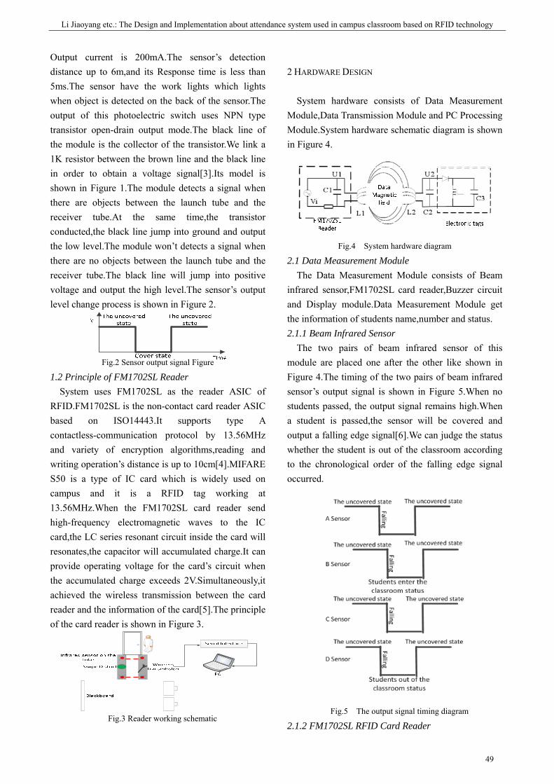
Li Jiaoyang etc.: The Design and Implementation about attendance system used in campus classroom based on RFID technology
49
Output current is 200mA.The sensor’s detection distance up to 6m,and its Response time is less than 5ms.The sensor have the work lights which lights when object is detected on the back of the sensor.The output of this photoelectric switch uses NPN type transistor open-drain output mode.The black line of the module is the collector of the transistor.We link a 1K resistor between the brown line and the black line in order to obtain a voltage signal[3].Its model is shown in Figure 1.The module detects a signal when there are objects between the launch tube and the receiver tube.At the same time,the transistor conducted,the black line jump into ground and output the low level.The module won’t detects a signal when there are no objects between the launch tube and the receiver tube.The black line will jump into positive voltage and output the high level.The sensor’s output level change process is shown in Figure 2.
Fig.2 Sensor output signal Figure
1.2 Principle of FM1702SL Reader System uses FM1702SL as the reader ASIC of
RFID.FM1702SL is the non-contact card reader ASIC based on ISO14443.It supports type A contactless-communication protocol by 13.56MHz and variety of encryption algorithms,reading and writing operation’s distance is up to 10cm[4].MIFARE S50 is a type of IC card which is widely used on campus and it is a RFID tag working at 13.56MHz.When the FM1702SL card reader send high-frequency electromagnetic waves to the IC card,the LC series resonant circuit inside the card will resonates,the capacitor will accumulated charge.It can provide operating voltage for the card’s circuit when the accumulated charge exceeds 2V.Simultaneously,it achieved the wireless transmission between the card reader and the information of the card[5].The principle of the card reader is shown in Figure 3.
Fig.3 Reader working schematic
2 HARDWARE DESIGN
System hardware consists of Data Measurement Module,Data Transmission Module and PC Processing Module.System hardware schematic diagram is shown in Figure 4.
Fig.4 System hardware diagram
2.1 Data Measurement Module The Data Measurement Module consists of Beam
infrared sensor,FM1702SL card reader,Buzzer circuit and Display module.Data Measurement Module get the information of students name,number and status. 2.1.1 Beam Infrared Sensor
The two pairs of beam infrared sensor of this module are placed one after the other like shown in Figure 4.The timing of the two pairs of beam infrared sensor’s output signal is shown in Figure 5.When no students passed, the output signal remains high.When a student is passed,the sensor will be covered and output a falling edge signal[6].We can judge the status whether the student is out of the classroom according to the chronological order of the falling edge signal occurred.
Fig.5 The output signal timing diagram
2.1.2 FM1702SL RFID Card Reader
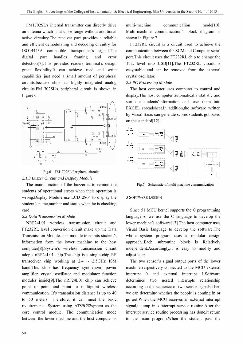
期 The English Proceedings of the College of Instrumentation & Electrical Engineering, Jilin University, in the Second Half of 2013
50
FM1702SL’s internal transmitter can directly drive an antenna which is at close range without additional active circuitry.The receiver part provides a reliable and efficient demodulating and decoding circuitry for ISO14443A compatible transponder’s signal.The digital part handles framing and error detection[7].This provides readers terminal’s design great flexibility.It can achieve read and write capabilities just need a small amount of peripheral circuits,because chip has highly integrated analog circuits.FM1702SL’s peripheral circuit is shown in Figure 6.
Fig.6 FM1702SL Peripheral circuits
2.1.3 Buzzer Circuit and Display Module The main function of the buzzer is to remind the
students of operational errors when their operation is wrong.Display Module use LCD12864 to display the student’s name,number and status when he is checking card. 2.2 Data Transmission Module
NRF24L01 wireless transmission circuit and FT232RL level conversion circuit make up the Data Transmission Module.This module transmits student’s information from the lower machine to the host computer[8].System’s wireless transmission circuit adopts nRF24L01 chip.The chip is a single-chip RF transceiver chip working at 2.4 ~ 2.5GHz ISM band.This chip has frequency synthesizer, power amplifier, crystal oscillator and modulator function modules inside[9].The nRF24L01 chip can achieve point to point and point to multipoint wireless communication. It’s transmission distance is up to 40 to 50 meters. Therefore, it can meet the basic requirements. System using AT89C52system as the core control module. The communication mode between the lower machine and the host computer is
multi-machine communication mode[10]. Multi-machine communication’s block diagram is shown in Figure 7.
FT232RL circuit is a circuit used to achieve the communication between the SCM and Computer serial port.This circuit uses the FT232RL chip to change the TTL level into USB[11].The FT232RL circuit is easy,stable and can be removed from the external crystal oscillator. 2.3 PC Processing Module
The host computer uses computer to control and display.The host computer automatically statistic and sort out students’information and save them into EXCEL spreadsheet.In addition,the software written by Visual Basic can generate scores students got based on the standard[12].
Fig.7 Schematic of multi-machine communication
3 SOFTWARE DESIGN
Since 51 MCU kernel supports the C programming language,so we use the C language to develop the lower machine’s software[13].The host computer uses Visual Basic language to develop the software.The whole system program uses a modular design approach..Each subroutine block is Relatively independent.Accordingly,it is easy to modify and adjust later.
The two sensor’s signal output ports of the lower machine respectively connected to the MCU external interrupt 0 and external interrupt 1.Software determines two nested interrupts relationship according to the sequence of two sensor signals.Then we can determine whether the people is coming in or go out.When the MCU receives an external interrupt signal,it jump into interrupt service routine.After the interrupt service routine processing has done,it return to the main program.When the student pass the
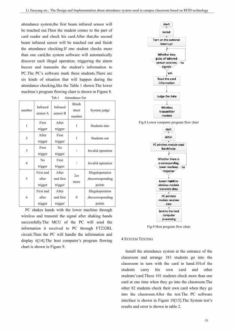
Li Jiaoyang etc.: The Design and Implementation about attendance system used in campus classroom based on RFID technology
51
attendance system,the first beam infrared sensor will be touched out.Then the student comes to the part of card reader and check his card.After that,the second beam infrared sensor will be touched out and finish the attendance checking.If one student checks more than one card,the system software will automatically discover such illegal operation, triggering the alarm buzzer and transmits the student’s information to PC.The PC’s software mark these students.There are six kinds of situation that will happen during the attendance checking,like the Table 1 shown.The lower machine’s program flowing chart is shown in Figure 8.
Tab.1 Attendance list
number Infrared
sensor A
Infrared
sensor B
Brush
sheet
number
System judge
1 First
trigger
After
trigger 1 Students into
2 After
trigger
First
trigger 1 Students out
3 First
trigger
No
trigger \ Invalid operation
4 No
trigger
First
trigger \ Invalid operation
5
First and
after
trigger
After
and first
trigger
2or
more
Illegaloperation
,thecorresponding
points
6
First and
after
trigger
After
and first
trigger
0
Illegaloperation
,thecorresponding
points
PC shakes hands with the lower machine through wireless and transmit the signal after shaking hands successfully.The MCU of the PC will send the information it received to PC through FT232RL circuit.Then the PC will handle the information and display it[14].The host computer’s program flowing chart is shown in Figure 9.
Fig.8 Lower computer program flow chart
Fig.9 Host program flow chart
4 SYSTEM TESTING
Install the attendance system at the entrance of the classroom and arrange 183 students go into the classroom in turn with the card in hand.101of the students carry his own card and other students’card.These 101 students check more than one card at one time when they go into the classroom.The other 82 students check their own card when they go into the classroom.After the test.The PC software interface is shown in Figure 10[15].The System test’s results and error is shown in table 2.
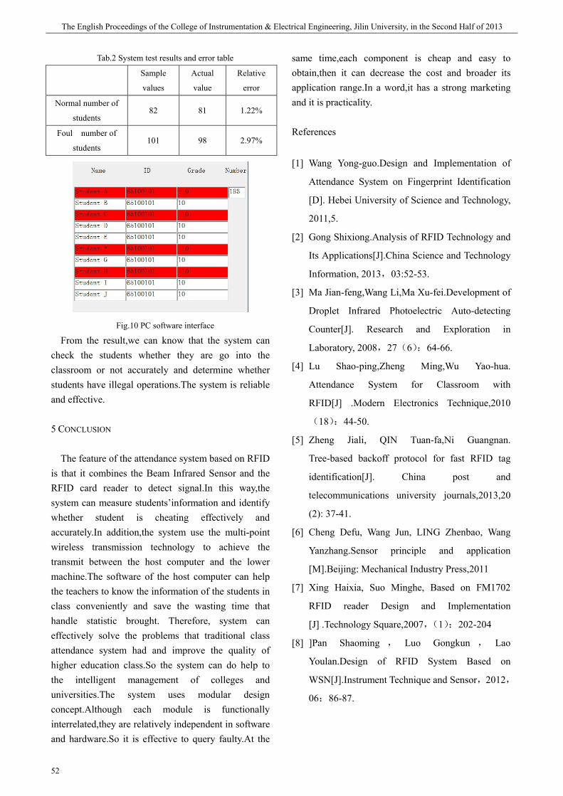
期 The English Proceedings of the College of Instrumentation & Electrical Engineering, Jilin University, in the Second Half of 2013
52
Tab.2 System test results and error table
Sample
values
Actual
value
Relative
error
Normal number of
students 82 81 1.22%
Foul number of
students 101 98 2.97%
Fig.10 PC software interface
From the result,we can know that the system can check the students whether they are go into the classroom or not accurately and determine whether students have illegal operations.The system is reliable and effective.
5 CONCLUSION
The feature of the attendance system based on RFID is that it combines the Beam Infrared Sensor and the RFID card reader to detect signal.In this way,the system can measure students’information and identify whether student is cheating effectively and accurately.In addition,the system use the multi-point wireless transmission technology to achieve the transmit between the host computer and the lower machine.The software of the host computer can help the teachers to know the information of the students in class conveniently and save the wasting time that handle statistic brought. Therefore, system can effectively solve the problems that traditional class attendance system had and improve the quality of higher education class.So the system can do help to the intelligent management of colleges and universities.The system uses modular design concept.Although each module is functionally interrelated,they are relatively independent in software and hardware.So it is effective to query faulty.At the
same time,each component is cheap and easy to obtain,then it can decrease the cost and broader its application range.In a word,it has a strong marketing and it is practicality.
References
[1] Wang Yong-guo.Design and Implementation of
Attendance System on Fingerprint Identification
[D]. Hebei University of Science and Technology,
2011,5.
[2] Gong Shixiong.Analysis of RFID Technology and
Its Applications[J].China Science and Technology
Information, 2013,03:52-53.
[3] Ma Jian-feng,Wang Li,Ma Xu-fei.Development of
Droplet Infrared Photoelectric Auto-detecting
Counter[J]. Research and Exploration in
Laboratory, 2008,27(6):64-66.
[4] Lu Shao-ping,Zheng Ming,Wu Yao-hua.
Attendance System for Classroom with
RFID[J] .Modern Electronics Technique,2010
(18):44-50.
[5] Zheng Jiali, QIN Tuan-fa,Ni Guangnan.
Tree-based backoff protocol for fast RFID tag
identification[J]. China post and
telecommunications university journals,2013,20
(2): 37-41.
[6] Cheng Defu, Wang Jun, LING Zhenbao, Wang
Yanzhang.Sensor principle and application
[M].Beijing: Mechanical Industry Press,2011
[7] Xing Haixia, Suo Minghe, Based on FM1702
RFID reader Design and Implementation
[J] .Technology Square,2007,(1):202-204
[8] ]Pan Shaoming , Luo Gongkun , Lao
Youlan.Design of RFID System Based on
WSN[J].Instrument Technique and Sensor,2012,
06:86-87.

Li Jiaoyang etc.: The Design and Implementation about attendance system used in campus classroom based on RFID technology
53
[9] Liu Zhiping, Zhao Guoliang.Short-range wireless
data transmission based on nRF24L01[J].Applied
Science and Technology, 2008,35(3):55-58
[10] Qian Chenghui,Han Xiaohui, Wang Ying, Ling
Zhenbao, Gao Le.Statistics System Design on
Flow of People Based on CC1100 Wireless
Transmission[J]. Journal of Jilin University
(Information Science Edition),2012,30(05):
497-502.
[11] Baozhao Wei, Wang Lin, Xu Qi, Li Yunfei.A
Converter Module Design about USB-RS232
Based on FT232R[J]. Computer Knowledge and
Technology, 2008,(7):1204-1206
[12] Su Zhuanfang.Visual Basic Programming [M].
Higher Education Press, 2007,5
[13] Guo Tianxiang.51 single-chip C language tutorial
[M].Beijing: Electronic Industry Press, 2009.
[14] Li Wenfeng,Wang Ruchuan ,Sun Lijuan.MiniTE:
data acquisition routing for wireless sensor
networks[J].China post and telecommunications
university journals,2009, 16(1):16-21.
[15] Wei Caiqiao,Wang Xiaoguang,Jiao Mandun. The
Output of Complex Data Report Based on VB and
EXCEL[J].Journal of North China Institute of
Astronautic Engineer,2005,15(1):3-7.
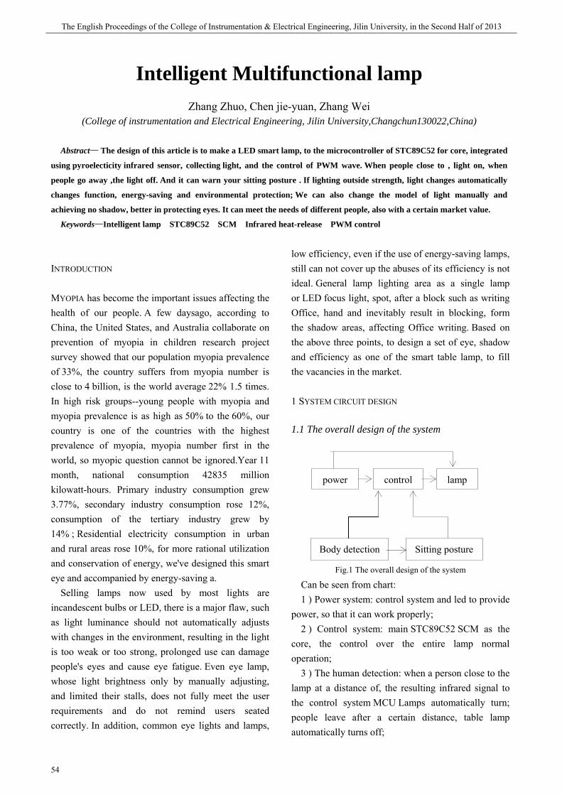
期 The English Proceedings of the College of Instrumentation & Electrical Engineering, Jilin University, in the Second Half of 2013
54
Intelligent Multifunctional lamp
Zhang Zhuo, Chen jie-yuan, Zhang Wei (College of instrumentation and Electrical Engineering, Jilin University,Changchun130022,China)
Abstract— The design of this article is to make a LED smart lamp, to the microcontroller of STC89C52 for core, integrated
using pyroelecticity infrared sensor, collecting light, and the control of PWM wave. When people close to , light on, when
people go away ,the light off. And it can warn your sitting posture . If lighting outside strength, light changes automatically
changes function, energy-saving and environmental protection; We can also change the model of light manually and
achieving no shadow, better in protecting eyes. It can meet the needs of different people, also with a certain market value.
Keywords—Intelligent lamp STC89C52 SCM Infrared heat-release PWM control
INTRODUCTION
MYOPIA has become the important issues affecting the health of our people. A few daysago, according to China, the United States, and Australia collaborate on prevention of myopia in children research project survey showed that our population myopia prevalence of 33%, the country suffers from myopia number is close to 4 billion, is the world average 22% 1.5 times. In high risk groups--young people with myopia and myopia prevalence is as high as 50% to the 60%, our country is one of the countries with the highest prevalence of myopia, myopia number first in the world, so myopic question cannot be ignored.Year 11 month, national consumption 42835 million kilowatt-hours. Primary industry consumption grew 3.77%, secondary industry consumption rose 12%, consumption of the tertiary industry grew by 14% ; Residential electricity consumption in urban and rural areas rose 10%, for more rational utilization and conservation of energy, we've designed this smart eye and accompanied by energy-saving a.
Selling lamps now used by most lights are incandescent bulbs or LED, there is a major flaw, such as light luminance should not automatically adjusts with changes in the environment, resulting in the light is too weak or too strong, prolonged use can damage people's eyes and cause eye fatigue. Even eye lamp, whose light brightness only by manually adjusting, and limited their stalls, does not fully meet the user requirements and do not remind users seated correctly. In addition, common eye lights and lamps,
low efficiency, even if the use of energy-saving lamps, still can not cover up the abuses of its efficiency is not ideal. General lamp lighting area as a single lamp or LED focus light, spot, after a block such as writing Office, hand and inevitably result in blocking, form the shadow areas, affecting Office writing. Based on the above three points, to design a set of eye, shadow and efficiency as one of the smart table lamp, to fill the vacancies in the market.
1 SYSTEM CIRCUIT DESIGN
1.1 The overall design of the system
Fig.1 The overall design of the system
Can be seen from chart: 1 ) Power system: control system and led to provide
power, so that it can work properly; 2 ) Control system: main STC89C52 SCM as the
core, the control over the entire lamp normal operation;
3 ) The human detection: when a person close to the lamp at a distance of, the resulting infrared signal to the control system MCU Lamps automatically turn; people leave after a certain distance, table lamp automatically turns off;
power control lamp
Body detection Sitting posture
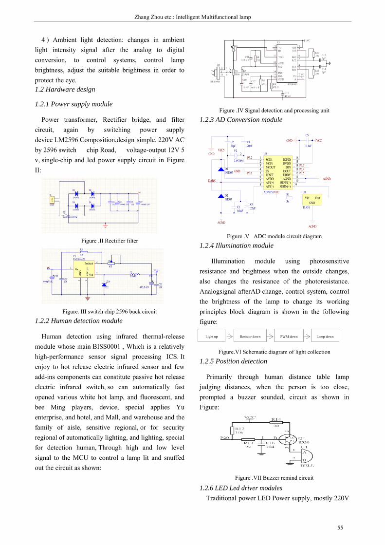
Zhang Zhou etc.: Intelligent Multifunctional lamp
55
4 ) Ambient light detection: changes in ambient light intensity signal after the analog to digital conversion, to control systems, control lamp brightness, adjust the suitable brightness in order to protect the eye. 1.2 Hardware design
1.2.1 Power supply module
Power transformer, Rectifier bridge, and filter circuit, again by switching power supply device LM2596 Composition,design simple. 220V AC by 2596 switch chip Road, voltage-output 12V 5 v, single-chip and led power supply circuit in Figure II:
Figure .II Rectifier filter
Figure. III switch chip 2596 buck circuit
1.2.2 Human detection module
Human detection using infrared thermal-release module whose main BISS0001 , Which is a relatively high-performance sensor signal processing ICS. It enjoy to hot release electric infrared sensor and few add-ins components can constitute passive hot release electric infrared switch, so can automatically fast opened various white hot lamp, and fluorescent, and bee Ming players, device, special applies Yu enterprise, and hotel, and Mall, and warehouse and the family of aisle, sensitive regional, or for security regional of automatically lighting, and lighting, special for detection human, Through high and low level signal to the MCU to control a lamp lit and snuffed out the circuit as shown:
Figure .IV Signal detection and processing unit
1.2.3 AD Conversion module
DGND 16
DVDD 15
DIN 14
DOUT 13
DRDY 12
AGND 11
REFIN(-) 10
REFIN(+) 9AIN(-)8 AIN(+)7 AVDD6 RESET5 CS4 MCOUT3 MCIN2 SCLK1U2
AD7715 1
D1IN4007
D2N4007
VCC5
AGND
GND
0.1uFC1
20pFC2
20pFC3
1 2Y2
2.4576M
GND
22uFC4
0.1uF
C5GND VCC
AGND
Vin VoutGND
U3
TL431
AGND
VCC
P3.2
P3.6
P3.3P3.4P3.5
3k
R1
DARK
Figure .V ADC module circuit diagram
1.2.4 Illumination module
Illumination module using photosensitive resistance and brightness when the outside changes, also changes the resistance of the photoresistance. Analogsignal afterAD change, control system, control the brightness of the lamp to change its working principles block diagram is shown in the following figure:
Figure.VI Schematic diagram of light collection
1.2.5 Position detection
Primarily through human distance table lamp judging distances, when the person is too close, prompted a buzzer sounded, circuit as shown in Figure:
Figure .VII Buzzer remind circuit
1.2.6 LED Led driver modules Traditional power LED Power supply, mostly 220V
Light up Resistor down PWM down Lamp down
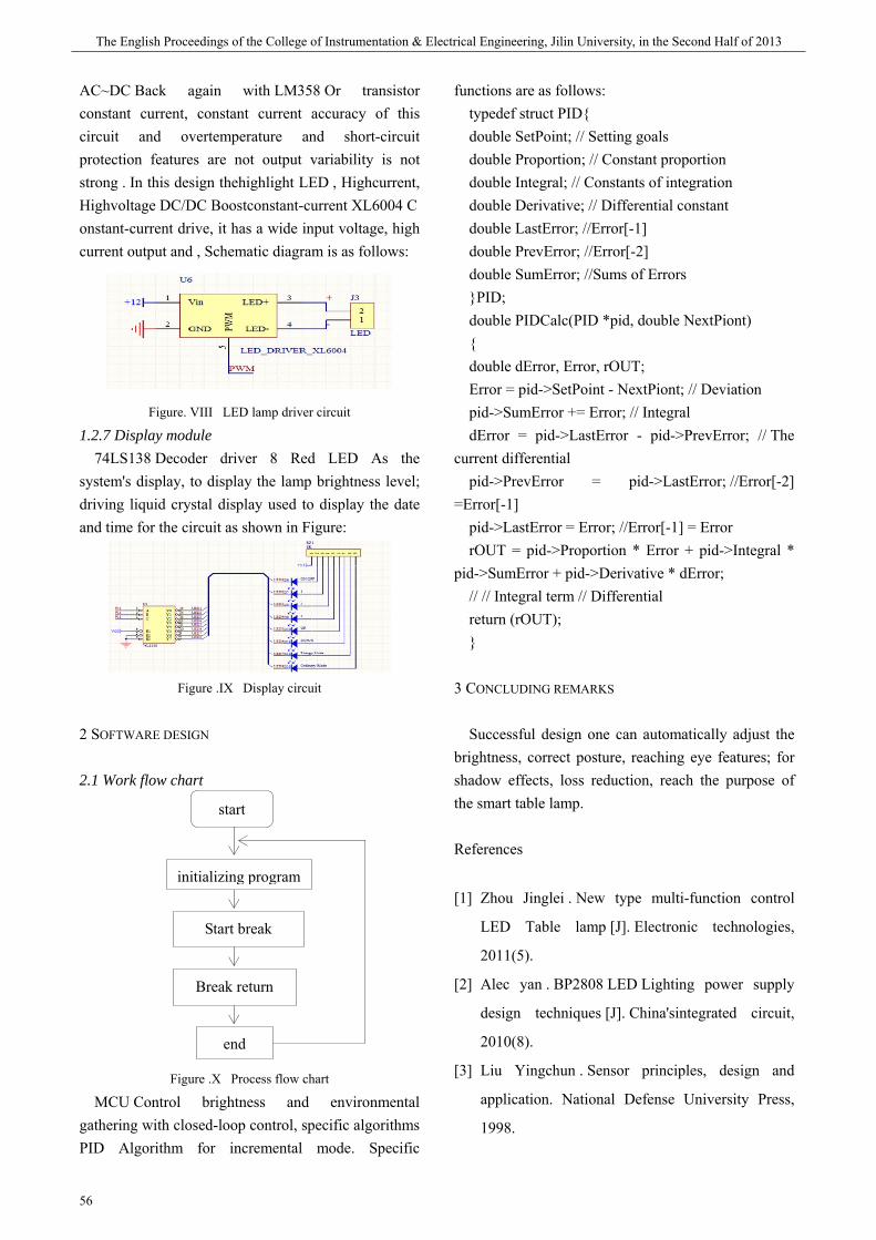
期 The English Proceedings of the College of Instrumentation & Electrical Engineering, Jilin University, in the Second Half of 2013
56
AC~DC Back again with LM358 Or transistor constant current, constant current accuracy of this circuit and overtemperature and short-circuit protection features are not output variability is not strong . In this design thehighlight LED , Highcurrent, Highvoltage DC/DC Boostconstant-current XL6004 Constant-current drive, it has a wide input voltage, high current output and , Schematic diagram is as follows:
Figure. VIII LED lamp driver circuit
1.2.7 Display module 74LS138 Decoder driver 8 Red LED As the
system's display, to display the lamp brightness level; driving liquid crystal display used to display the date and time for the circuit as shown in Figure:
Figure .IX Display circuit
2 SOFTWARE DESIGN
2.1 Work flow chart
Figure .X Process flow chart
MCU Control brightness and environmental gathering with closed-loop control, specific algorithms PID Algorithm for incremental mode. Specific
functions are as follows: typedef struct PID double SetPoint; // Setting goals double Proportion; // Constant proportion double Integral; // Constants of integration double Derivative; // Differential constant double LastError; //Error[-1] double PrevError; //Error[-2] double SumError; //Sums of Errors PID; double PIDCalc(PID *pid, double NextPiont) double dError, Error, rOUT; Error = pid->SetPoint - NextPiont; // Deviation pid->SumError += Error; // Integral dError = pid->LastError - pid->PrevError; // The
current differential pid->PrevError = pid->LastError; //Error[-2]
=Error[-1] pid->LastError = Error; //Error[-1] = Error rOUT = pid->Proportion * Error + pid->Integral *
pid->SumError + pid->Derivative * dError; // // Integral term // Differential return (rOUT);
3 CONCLUDING REMARKS
Successful design one can automatically adjust the brightness, correct posture, reaching eye features; for shadow effects, loss reduction, reach the purpose of the smart table lamp.
References
[1] Zhou Jinglei . New type multi-function control
LED Table lamp [J]. Electronic technologies,
2011(5).
[2] Alec yan . BP2808 LED Lighting power supply
design techniques [J]. China'sintegrated circuit,
2010(8).
[3] Liu Yingchun . Sensor principles, design and
application. National Defense University Press,
1998.
initializing program
Start break
Break return
end
start

Zhang Zhou etc.: Intelligent Multifunctional lamp
57
[4] Peng Jinsong, Li Kwan . Constant current source
LED Touch table lamp design [J]. Shanxi
electronic technology, 2007(2).
[5] Beijing University of Aeronautics and
Astronautics press,2003.
[6] Tong Shibai . Analog electronics[m]. Beijing:
higher education press , 1999.
[7] Yang Bangwen . Collection of practical power
circuit[m]. Beijing : Publishing House of
electronics industry , 2003.
[8] Ding Yuanjie . Single chip microcomputer
principle and application[M]. Beijing: China
machine press , 2001:1.
[9] the Sun , Sun Xiaobin . Sensing technology[M].
Beijing : Publishing House of electronics industry ,
2001.
[10] Zhao Jiwen . Circuit design of sensor and its
application [M]. , Beijing : science press , 2002.
[11] Huang Jichang . Application manual of electronic
components [M]. Beijing : people's posts and
telecommunications publishing house , 2004.
[12] He Xicai . The sensor circuit and its
application[M]. Beijing : Publishing House of
electronics industry , 2001.
[13] R. JH iggens. E lec tron ics and Analog In teg ra
ted C ircu its[M ]. N. J. Pren tice- H a ll Inc, 2001.
[14] C ray C, Sw inhoeC F, M y in,l et al. Ta rget con
tro lled in fusion o f ketam ine as ana lgessia for
TIV A w ith propo fo l. Can. J Anesth, 1999,
40:957.
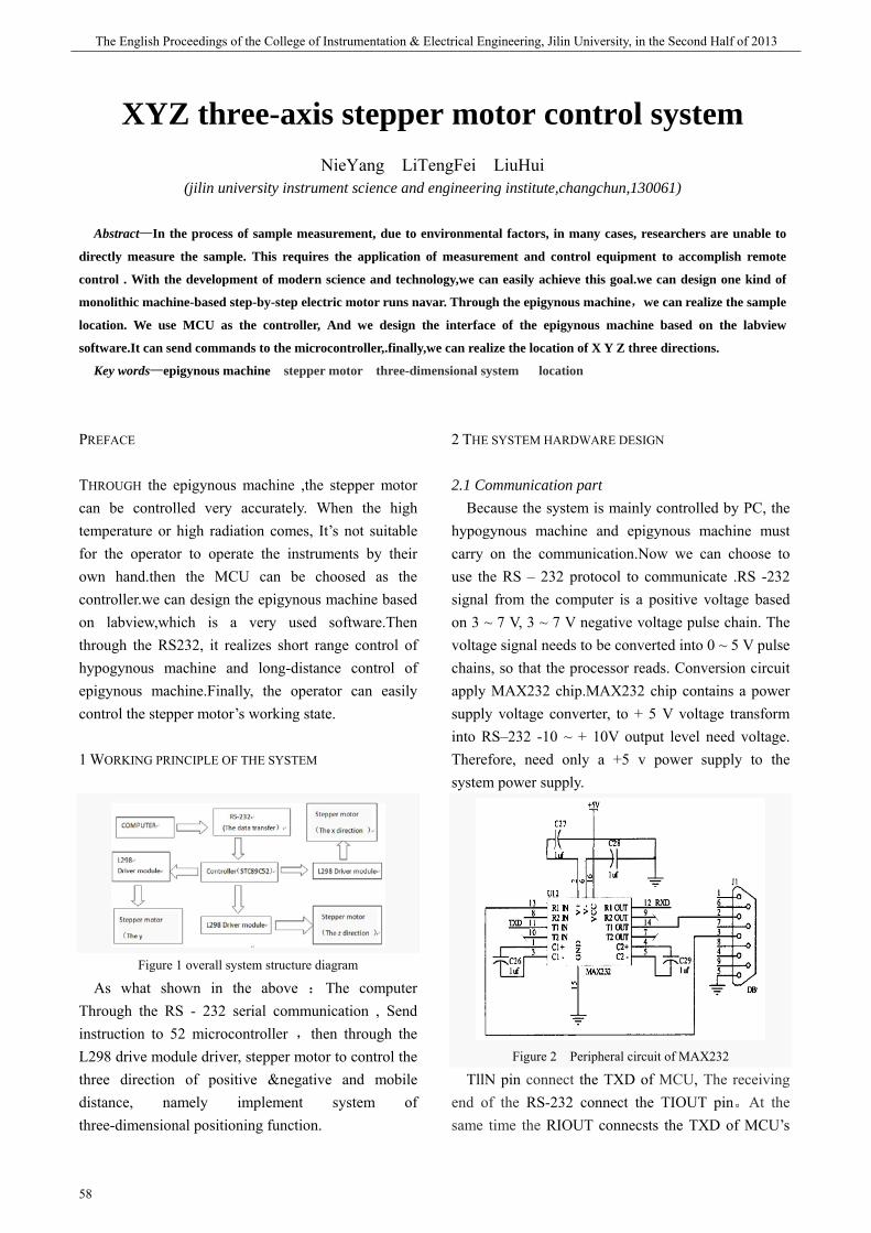
期 The English Proceedings of the College of Instrumentation & Electrical Engineering, Jilin University, in the Second Half of 2013
58
XYZ three-axis stepper motor control system
NieYang LiTengFei LiuHui (jilin university instrument science and engineering institute,changchun,130061)
Abstract—In the process of sample measurement, due to environmental factors, in many cases, researchers are unable to
directly measure the sample. This requires the application of measurement and control equipment to accomplish remote
control . With the development of modern science and technology,we can easily achieve this goal.we can design one kind of
monolithic machine-based step-by-step electric motor runs navar. Through the epigynous machine,we can realize the sample
location. We use MCU as the controller, And we design the interface of the epigynous machine based on the labview
software.It can send commands to the microcontroller,.finally,we can realize the location of X Y Z three directions.
Key words—epigynous machine stepper motor three-dimensional system location
PREFACE
THROUGH the epigynous machine ,the stepper motor can be controlled very accurately. When the high temperature or high radiation comes, It’s not suitable for the operator to operate the instruments by their own hand.then the MCU can be choosed as the controller.we can design the epigynous machine based on labview,which is a very used software.Then through the RS232, it realizes short range control of hypogynous machine and long-distance control of epigynous machine.Finally, the operator can easily control the stepper motor’s working state.
1 WORKING PRINCIPLE OF THE SYSTEM
Figure 1 overall system structure diagram
As what shown in the above :The computer Through the RS - 232 serial communication , Send instruction to 52 microcontroller ,then through the L298 drive module driver, stepper motor to control the three direction of positive &negative and mobile distance, namely implement system of three-dimensional positioning function.
2 THE SYSTEM HARDWARE DESIGN
2.1 Communication part Because the system is mainly controlled by PC, the
hypogynous machine and epigynous machine must carry on the communication.Now we can choose to use the RS – 232 protocol to communicate .RS -232 signal from the computer is a positive voltage based on 3 ~ 7 V, 3 ~ 7 V negative voltage pulse chain. The voltage signal needs to be converted into 0 ~ 5 V pulse chains, so that the processor reads. Conversion circuit apply MAX232 chip.MAX232 chip contains a power supply voltage converter, to + 5 V voltage transform into RS–232 -10 ~ + 10V output level need voltage. Therefore, need only a +5 v power supply to the system power supply.
Figure 2 Peripheral circuit of MAX232
TllN pin connect the TXD of MCU, The receiving end of the RS-232 connect the TIOUT pin。At the same time the RIOUT connecsts the TXD of MCU’s
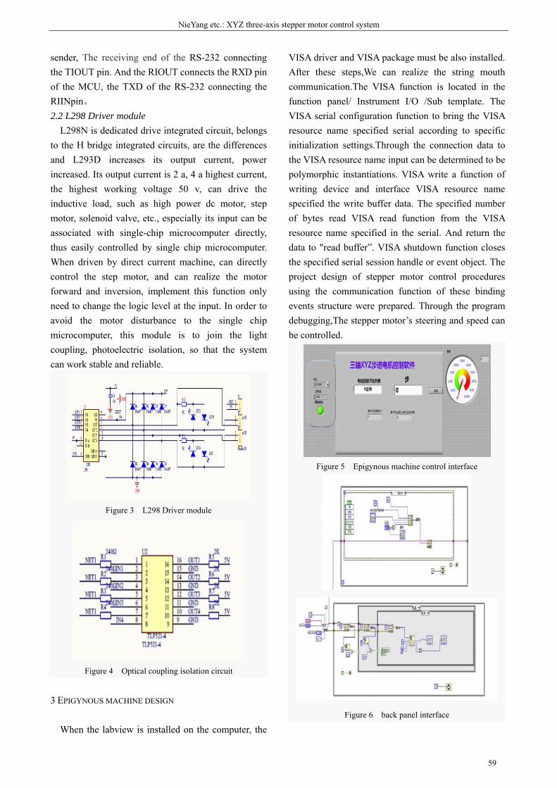
NieYang etc.: XYZ three-axis stepper motor control system
59
sender, The receiving end of the RS-232 connecting the TIOUT pin. And the RIOUT connects the RXD pin of the MCU, the TXD of the RS-232 connecting the RIINpin。 2.2 L298 Driver module
L298N is dedicated drive integrated circuit, belongs to the H bridge integrated circuits, are the differences and L293D increases its output current, power increased. Its output current is 2 a, 4 a highest current, the highest working voltage 50 v, can drive the inductive load, such as high power dc motor, step motor, solenoid valve, etc., especially its input can be associated with single-chip microcomputer directly, thus easily controlled by single chip microcomputer. When driven by direct current machine, can directly control the step motor, and can realize the motor forward and inversion, implement this function only need to change the logic level at the input. In order to avoid the motor disturbance to the single chip microcomputer, this module is to join the light coupling, photoelectric isolation, so that the system can work stable and reliable.
Figure 3 L298 Driver module
Figure 4 Optical coupling isolation circuit
3 EPIGYNOUS MACHINE DESIGN
When the labview is installed on the computer, the
VISA driver and VISA package must be also installed. After these steps,We can realize the string mouth communication.The VISA function is located in the function panel/ Instrument I/O /Sub template. The VISA serial configuration function to bring the VISA resource name specified serial according to specific initialization settings.Through the connection data to the VISA resource name input can be determined to be polymorphic instantiations. VISA write a function of writing device and interface VISA resource name specified the write buffer data. The specified number of bytes read VISA read function from the VISA resource name specified in the serial. And return the data to "read buffer”. VISA shutdown function closes the specified serial session handle or event object. The project design of stepper motor control procedures using the communication function of these binding events structure were prepared. Through the program debugging,The stepper motor’s steering and speed can be controlled.
Figure 5 Epigynous machine control interface
Figure 6 back panel interface
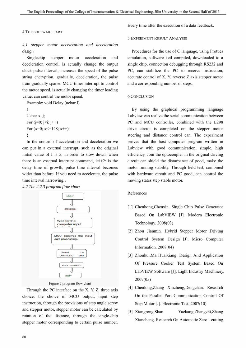
期 The English Proceedings of the College of Instrumentation & Electrical Engineering, Jilin University, in the Second Half of 2013
60
4 THE SOFTWARE PART
4.1 stepper motor acceleration and deceleration design
Singlechip stepper motor acceleration and deceleration control, is actually change the output clock pulse interval, increases the speed of the pulse string encryption, gradually, deceleration, the pulse train gradually sparse. MCU timer interrupt to control the motor speed, is actually changing the timer loading value, can control the motor speed.
Example: void Delay (uchar I) Uchar x, j; For (j=0; j<i; j++) For (x=0; x<=148; x++); In the control of acceleration and deceleration we
can put in a external interrupt, such as the original initial value of I is 5, in order to slow down, when there is an external interrupt command, i=i+2; is the delay time of growth, pulse time interval becomes wider than before. If you need to accelerate, the pulse time interval narrowing.。 4.2 The 2.2.3 program flow chart
Figure 7 program flow chart
Through the PC interface on the X, Y, Z, three axis choice, the choice of MCU output, input step instruction, through the provisions of step angle screw and stepper motor, stepper motor can be calculated by rotation of the distance, through the single-chip stepper motor corresponding to certain pulse number.
Every time after the execution of a data feedback.
5 EXPERIMENT RESULT ANALYSIS
Procedures for the use of C language, using Protues simulation, software keil compiled, downloaded to a single chip, connection debugging through RS232 and PC, can stabilize the PC to receive instruction, accurate control of X, Y, reverse Z axis stepper motor and a corresponding number of steps.
6 CONCLUSION
By using the graphical programming language Labview can realize the serial communication between PC and MCU controller, combined with the L298 drive circuit is completed on the stepper motor steering and distance control can. The experiment proves that the host computer program written in Labview with good communication, simple, high efficiency. Join the optocoupler in the original driving circuit can shield the disturbance of good, make the motor running stability. Through field test, combined with hardware circuit and PC good, can control the moving states step stable motor.
References
[1] Chenhong,Chenxin. Single Chip Pulse Generator
Based On LabVIEW [J]. Modern Electronic
Technology. 2008(03)
[2] Zhou Jianmin. Hybrid Stepper Motor Driving
Control System Design [J]. Micro Computer
Information. 2008(04)
[3] Zhouhui,Ma Huaixiang. Design And Application
Of Pressure Cooker Test System Based On
LabVIEW Software [J]. Light Industry Machinery.
2007(05)
[4] Chenlong,Zhang Xinzheng,Dengchan. Research
On the Parallel Port Communication Control Of
Step Motor [J]. Electronic Test. 2007(10)
[5] Xiangrong,Shan Yuekang,Zhangzhi,Zhang
Xiancheng. Research On Automatic Zero - cutting

NieYang etc.: XYZ three-axis stepper motor control system
61
System Of Steel Tape[J]. Journal of China Jiliang
University. 2006 (04)
[6] WangJunfeng,Song Wenai,Liuzhe. LabVIEW
Signal Processing System Based on Virtual
Experiment [J]. Foreign Electronic Measurement
Technology. 2006(10)
[7] Zhao Dongmei,Zhangbin.Labview Automatic
Speed Control Stepper Motor [J]. Micro Computer
Information. 2006(28)
[8] Sun Guanqun,Li Xiaoqing,Zhang Lisuo.SR
Design Of Speed Control System Of Motor[J].
Journal Of China Jiliang University. 2006(03)
[9] Chen Fangquan,Li Jianzhou,Ma Siwen. LabVIEW
Stepper Motor Drive Design And Its Application
Based On [J]. Journal of Shanghai University.
2006(01)
[10] Yanglin,Wang Xiaoguang. LabView Stepper
Motor Control [J]. Electric Drive. 2004(05)

期 The English Proceedings of the College of Instrumentation & Electrical Engineering, Jilin University, in the Second Half of 2013
62
The dormitory intelligent security alarm system based on GSM wireless communication
JiaoLei ZhaoYue WangZhengyu
Supervisor QiuChunling Abstract—A remote alarm system has been designed, which is based on GSM, and improved the traditional anti-theft
system of intelligent, localized hidden trouble. It with 51 single chip microcomputer as controller, and through GSM wireless
communication module, to our bedroom burglar alarm, fire alarm, temperature monitoring, expensive equipment monitoring,
gas leakage, site monitoring exception information to messages sent to the real-time called on the phone. This convenient
called personnel alarm in a very short time to make a precise and rapid emergency treatment.
Key words—GSM; Single chip microcomputer; Alarm system.
0 FOREWORD
AS an important part of society, the problems of safety management of colleges and universities are increasingly on the agenda. Students' dormitory is college students' life, study, rest home, is a place where students live longest and its security or not is directly related to the students' vital interests, affects the normal study, the life order of students and the school's harmony and stability. My campus is located in the downtown, liquid, and students' safety consciousness is not strong, so lead to theft, fire and other events occur which cause serious damage to the property and life safety of students. Therefore, the safety of the college students dormitory is related to the steady development of colleges and universities, and students' physical and mental health.
At present, the traditional security such as bedroom burglar mesh, window, etc exist in the actual use of other never stolen, Ann window close to the floor of the hidden trouble of the emergencies is not easy to escape. And common security alarm system on the market at present way of communication, such as fixed telephone dial-up are easy to be a rogue in front of the house to cut off the telephone line is busy or malicious, make its failure in critical moment. Ethernet are also faced with the hidden trouble of the line is cut off; The cluster system power consumption is very big, network building and maintenance costs are very high, and need to purchase a fixed frequency
point. In order to solve these existing hidden trouble, dormitory wireless burglar alarm system based on GSM short message module is designed, and it is no longer dependent on cable telephone alarm, but with the aid of the most reliable, most mature GSM mobile network, with the most intuitive form of short message or phone, the place for the alarm directly to reflect to the to the user's mobile phone.
1 SYSTEM OVERALL SCHEME IS INTRODUCED
This intelligent alarm system based on 51 single chip microcomputer as the core processor, its overall structure are shown in figure 1 below. It mainly adopts TS35i as the main communication module to collect signal communication alarm. TC35i is Siemens company introduced GSM wireless communication module industry, it is driven by the AT command control system alarm controller test top-up SIM card, and will start the information to the communication module to achieve activation network status, and then send alarm information by microwave antenna to achieve short message, even dial the preset receiving alarm telephone number [1]. First of all, the system of various sensors which have been dealt with by SCM are collected, and then output to the LCD, as a way to monitor the situation of the dormitory, and then through the TC35i communication module, the abnormal situation to send to the preset phone number, in order to realize the remote monitoring and management of the user.

JiaoLei etc.: The dormitory intelligent security alarm system based on GSM wireless communication
63
This system mainly includes the following features: 1) real-time temperature monitoring. This system
through the temperature sensor 18 b20 collected information of temperature in the dormitory, and then the information through the single-chip microcomputer control output to the LCD. And start the buzzer when temperature is too high.
2) time showing reminders. By DS1302 time online, according to the current time can effectively remind residents, give warm prompt to the user.
3) remote monitoring alarm. Through the pyroelectric sensor, smoke sensor such as real-time monitoring of the house will be gathering information through single chip, and TC35i communication module to realize the remote communication, to inform the user of the house.
2 THE HARDWARE DESIGN
2.1 the main control unit module This design adopts 51 series of 89 c51 single chip
microcomputer as main control unit. AT89C51 is a low voltage, low power consumption, high performance CMOS8 a single-chip microcomputer, the combination of general microprocessor with Flash memory together, it can wipe again and again, so can effectively reduce the cost of development. It has 40 pins, 32 external bidirectional input / output (I / O) ports, also includes two external interrupt port, two 16-bit programmable timer counters, two full duplex serial port, it can be programmed according to conventional methods, can also be online programming. SCM system work constantly refresh RAM, appropriately processed data to the LCD display, if there is an exception, it will be sent via
SMS alarm message to a specific preset phone number, and make the appropriate measures to inform heads of households, achieve dormitory remote security. 2.2 the pyroelectric infrared module
The body has a constant temperature, generally at 37 , it will emit a lot of infrared around 10μm. Human body emits infrared light through the Fresnel sheet enhanced infrared sensors gather source. Pyroelectric infrared sensor element, this element in the human body receives infrared radiation temperature changes will be lost when the charge balance outwards released charge, the subsequent processing circuit has been tested and will be able to generate an alarm signal. Pyroelectric infrared sensor itself has not made any type of radiation advantages, and the device power consumption, good concealment, low prices. But it is also subject to various sources of heat, light interference. The design we use HC-SR501 models. It uses LHI778 probe design, high sensitivity, high reliability, low voltage operation mode, widely used in various auto-sensing electrical equipment [2]. 2.3 temperature and smoke sensors module
The design uses MQ-2-type smoke sensor, smoke sensor of this type of high sensitivity, fast response, anti-interference ability, long life, etc. [3]. With DS18B20 temperature sensor senses the room temperature changes, and use LCD1602 display. Dormitory fire or going to happen, I also smoke or gas leak sensor will detect the concentration of pollutant gases, when it reaches a certain concentration, the buzzer is activated and an alarm signal. 2.4 GSM communication module
GSM communication module select TC35i, it is a new version of Siemens industrial GSM module a support Chinese short message industrial-grade GSM
Figure 1 overall structure
Temperature
Smoke sensor
Hall sensor
Pyroelectric infrared sensor
Single chip microcomputer main system
GSM communication module
Alarm circuit
The LCD display module

期 The English Proceedings of the College of Instrumentation & Electrical Engineering, Jilin University, in the Second Half of 2013
64
module [4]. GSM short message in Chinese is in accordance with the PDU (Protocol Data Unit) format, send or receive up to 70 Chinese characters, Chinese characters according to the UNICODE encoding, unlike computer Chinese character coding [5]. SCM send SMS command to the GSM module, GSM module can identify the command and send information to a user's phone number. Message content for reminding, safety accident happened such as gas leak, the sensor will be sent via single-chip computer command prompt warning messages to residents, these messages are programmed in advance, according to the type of accident direct call. 2.5 other modules
Other module and alarm circuit, it is when each sensor detects the abnormal signal is sent to the microcontroller, through the single-chip microcomputer control. And LCD1602 display screen is used to time and temperature of each module according to the status of the module. Also includes valuables detection module, which is the use of Hall sensors to monitor valuables detection module.
3 SOFTWARE DESIGN
The system uses a microcontroller as the main controller, when the system boots after power on, single-chip, GSM module initialization, the microcontroller initialization includes selecting operating mode, initialize the variable parameters, flags, etc., and then run in the main function. Where C language program includes a display shows the temperature sensor to the temperature value, and pyroelectric infrared, smoke sensors perceive external abnormalities acquisition value delivery to the microcontroller, then controlled by the microcontroller TC35i pass through remote monitoring terminal that household. Detailed flowchart is shown in Figure 2.
Figure 2 temperature respectively. Smoke. Infrared. Valuables
alarm message content
4 DESIGN RESULT AND ANALYSIS
The design of the wireless remote alarm when the measured reflect good, and it also can achieve the desired function. In the end, the text messages which sent to the user's results by mobile phone are shown in figure 3 below .And this design has the advantages of low cost and good reliability, high precision, easy to install. But also question the safety of the residents have a good prevention role. It can effectively avoid the loss of the user. Again due to the system of many functional solve the similar devices on the market of the defect of single function, the subsequent market promotion will have very good advantage.
Figure 3. Flow chart of system software
Reference
[1] Sony Ericsson Mobile Communications.
GR47/GR48 Design Guidelines.2003.
[2] baidu library. HC - SR501 specification. [DB/OL].
Baidu: http://wenku.baidu.com/view/ 05a3d684e
53a580216fcfec1. html

JiaoLei etc.: The dormitory intelligent security alarm system based on GSM wireless communication
65
[3] baidu library. MQ - 2 specification. [DB/OL].
Baidu: http://wenku.baidu.com/view/4bfa221c
fad6195f312ba608.html
[4] Wu Qing, Wu Bo. Based on TC35i GSM alarm
system design and implementation
Microcomputer information, 2009, 25; 1 to 2.
[5] Huang Xianshu. Engineering data gathering
remote monitoring system of GSM short message.
Microprocessor. 2010.6.

期 The English Proceedings of the College of Instrumentation & Electrical Engineering, Jilin University, in the Second Half of 2013
66
A post-disaster Detection Rescue Robot System Design
HU Rui-fan, WANG Hong-chao, PENG Yi-shuai
(College of insrumentation and Electrical Engineering, Jilin University,Changchun 130022,China) Abstract—For the frequent occurrence of natural disasters in recent years, the status of the rescue work difficult to design a
post-disaster relief robot system. System is divided into a remote monitoring control station and robotic body. Robotic body is
equipped with sophisticated sensor systems, motion control planning system, real-time communications and reliable actuators
etc, mounted night vision CCD camera, 512 * 582 resolution, real-time images obtained by pyroelectric infrared detection
module detects human radiation energy, looking upon rescue personnel, and designing automatic obstacle avoidance device to
prevent the robot collision .Remote monitor control station equipped with the corresponding management software, through
the transmission of image real-time remote control of the robot, observing and analyzing image information, getting the
position of the second accident -prone ,improving rescue efficiency and safety.Robotic system data and image information
through a wireless real-time transmission, small size, fast response, practical, it has a broad market prospect.
Key words—disaster relief; robot; sensor system; real-time communication; remote monitoring
0 PREFACE
GLOBAL frequent disasters in recent years, has brought people's lives and property damage. The most urgent thing is to search and rescue after disaster survivors trapped in the ruins. How to safely and effectively to search for survivors and timely detection of relief has become a major social problem at present. Post-disaster complicated scene environment to the rescuers and survivors are of great security threat, will hamper rescue work quickly and efficiently. Using the rescue robot for auxiliary search and rescue is an effective means to solve this problem [1].
The characteristics of the rescue robot has high flexibility and maneuverability is strong, and has a good grade and obstacle capability, able to adapt to field a variety of geographical environment, at the same time in the process of rescue can quickly determine the position of the survivors, and all kinds of changes that can detect the scene of the accident in order to prevent the secondary accident. Rescue robot that can overcome the traditional relief of low working efficiency, large rescue equipment is not stable, flexible and rescue fast, easy to carry and adaptable to the environment, thus the rescue robot research has important significance.
Intelligent rescue robot is designed and developed
based on the background of earthquake relief, is a kind of can repair function, mark accident sites, to seek relief road of advanced equipment. Highly intelligent [2-3] and automation is another big characteristics of this work, is also one of the advantages of strong competitiveness. At the same time, adopt the advanced control system and algorithm, universality and applicability of the system to further strengthen [3], to be able to complete various tasks.
1 DESIGN OF THE SYSTEM
Detection after a disaster rescue robot is a machine, electricity, light, communication technologies such as integrated products [4], remote monitoring system and the robot body of two parts, can complete the life signals detection, location, and the implementation of the rescue mission. Mainly by the visual system, detection system, wireless communication and computer control parts [5]. Overall system diagram as shown in figure 1.
Fig.1 Overall system schematic
When rescue, rescue workers through the leading
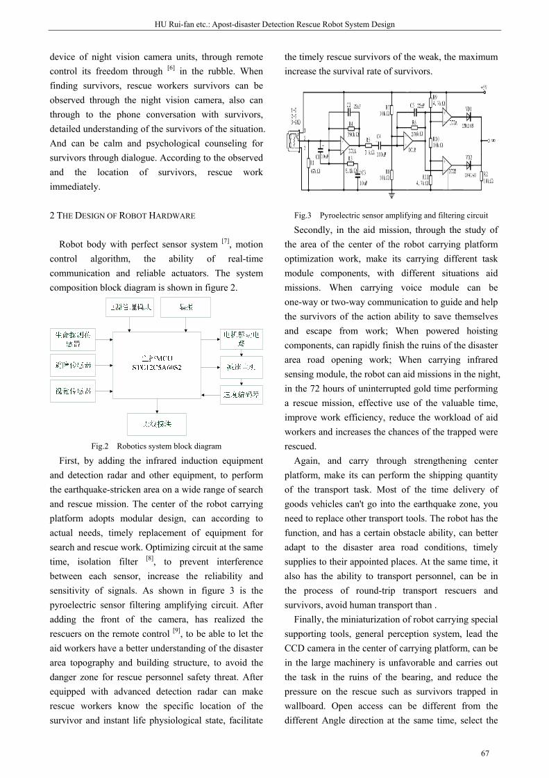
HU Rui-fan etc.: Apost-disaster Detection Rescue Robot System Design
67
device of night vision camera units, through remote control its freedom through [6] in the rubble. When finding survivors, rescue workers survivors can be observed through the night vision camera, also can through to the phone conversation with survivors, detailed understanding of the survivors of the situation. And can be calm and psychological counseling for survivors through dialogue. According to the observed and the location of survivors, rescue work immediately.
2 THE DESIGN OF ROBOT HARDWARE
Robot body with perfect sensor system [7], motion control algorithm, the ability of real-time communication and reliable actuators. The system composition block diagram is shown in figure 2.
Fig.2 Robotics system block diagram
First, by adding the infrared induction equipment and detection radar and other equipment, to perform the earthquake-stricken area on a wide range of search and rescue mission. The center of the robot carrying platform adopts modular design, can according to actual needs, timely replacement of equipment for search and rescue work. Optimizing circuit at the same time, isolation filter [8], to prevent interference between each sensor, increase the reliability and sensitivity of signals. As shown in figure 3 is the pyroelectric sensor filtering amplifying circuit. After adding the front of the camera, has realized the rescuers on the remote control [9], to be able to let the aid workers have a better understanding of the disaster area topography and building structure, to avoid the danger zone for rescue personnel safety threat. After equipped with advanced detection radar can make rescue workers know the specific location of the survivor and instant life physiological state, facilitate
the timely rescue survivors of the weak, the maximum increase the survival rate of survivors.
Fig.3 Pyroelectric sensor amplifying and filtering circuit
Secondly, in the aid mission, through the study of the area of the center of the robot carrying platform optimization work, make its carrying different task module components, with different situations aid missions. When carrying voice module can be one-way or two-way communication to guide and help the survivors of the action ability to save themselves and escape from work; When powered hoisting components, can rapidly finish the ruins of the disaster area road opening work; When carrying infrared sensing module, the robot can aid missions in the night, in the 72 hours of uninterrupted gold time performing a rescue mission, effective use of the valuable time, improve work efficiency, reduce the workload of aid workers and increases the chances of the trapped were rescued.
Again, and carry through strengthening center platform, make its can perform the shipping quantity of the transport task. Most of the time delivery of goods vehicles can't go into the earthquake zone, you need to replace other transport tools. The robot has the function, and has a certain obstacle ability, can better adapt to the disaster area road conditions, timely supplies to their appointed places. At the same time, it also has the ability to transport personnel, can be in the process of round-trip transport rescuers and survivors, avoid human transport than .
Finally, the miniaturization of robot carrying special supporting tools, general perception system, lead the CCD camera in the center of carrying platform, can be in the large machinery is unfavorable and carries out the task in the ruins of the bearing, and reduce the pressure on the rescue such as survivors trapped in wallboard. Open access can be different from the different Angle direction at the same time, select the
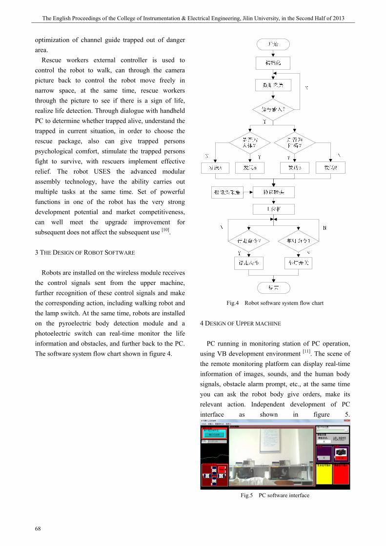
期 The English Proceedings of the College of Instrumentation & Electrical Engineering, Jilin University, in the Second Half of 2013
68
optimization of channel guide trapped out of danger area.
Rescue workers external controller is used to control the robot to walk, can through the camera picture back to control the robot move freely in narrow space, at the same time, rescue workers through the picture to see if there is a sign of life, realize life detection. Through dialogue with handheld PC to determine whether trapped alive, understand the trapped in current situation, in order to choose the rescue package, also can give trapped persons psychological comfort, stimulate the trapped persons fight to survive, with rescuers implement effective relief. The robot USES the advanced modular assembly technology, have the ability carries out multiple tasks at the same time. Set of powerful functions in one of the robot has the very strong development potential and market competitiveness, can well meet the upgrade improvement for subsequent does not affect the subsequent use [10].
3 THE DESIGN OF ROBOT SOFTWARE
Robots are installed on the wireless module receives the control signals sent from the upper machine, further recognition of these control signals and make the corresponding action, including walking robot and the lamp switch. At the same time, robots are installed on the pyroelectric body detection module and a photoelectric switch can real-time monitor the life information and obstacles, and further back to the PC. The software system flow chart shown in figure 4.
Fig.4 Robot software system flow chart
4 DESIGN OF UPPER MACHINE
PC running in monitoring station of PC operation, using VB development environment [11]. The scene of the remote monitoring platform can display real-time information of images, sounds, and the human body signals, obstacle alarm prompt, etc., at the same time you can ask the robot body give orders, make its relevant action. Independent development of PC interface as shown in figure 5.
Fig.5 PC software interface
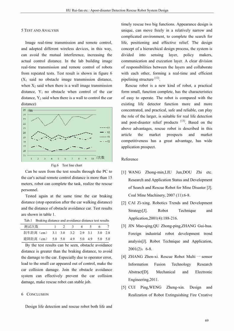
HU Rui-fan etc.: Apost-disaster Detection Rescue Robot System Design
69
5 TEST AND ANALYSIS
Image real-time transmission and remote control, and adopted different wireless devices, in this way, can avoid the mutual interference, increasing the actual control distance. In the lab building image real-time transmission and remote control of robots from repeated tests. Test result is shown in figure 6 (X1 said no obstacle image transmission distance, when X2 said when there is a wall image transmission distance, Y1 no obstacle when control of the car distance, Y2 said when there is a wall to control the car distance)
Fig.6 Test line chart
Can be seen from the test results through the PC to the car's actual remote control distance is more than 15 meters, robot can complete the task, realize the rescue personnel.
Tested again at the same time the car braking distance (stop operation after the car walking distance) and the distance of obstacle avoidance car. Test results are shown in table 1.
Tab.1 Braking distance and avoidance distance test results
测试次数 1 2 3 4 5 6 7
刹车距离(cm) 3.1 3.0 3.2 2.9 3.1 3.0 2.8
避障距离(cm) 5.0 5.0 4.9 5.0 4.9 5.0 5.0
By the test results can be seen, obstacle avoidance distance is greater than the braking distance, to avoid the damage to the car. Especially due to operator error, lead to the small car appeared out of control, make the car collision damage. Join the obstacle avoidance system can effectively prevent the car collision damage, make rescue robot can stable job.
6 CONCLUSION
Design life detection and rescue robot both life and
timely rescue two big functions. Appearance design is unique, can move freely in a relatively narrow and complicated environment, to complete the search for life, positioning and effective relief. The design concept of a hierarchical design process, the system is divided into sensing layer, policy makers, communication and execution layer. A clear division of responsibilities between the layers and collaborate with each other, forming a real-time and efficient pipelining structure [12].
Rescue robot is a new kind of robot, a practical form small, function complete, has the characteristics of easy to operate. The robot is compared with the existing life detector function more and more concentrated, and practical, safe and reliable, can play the role of the larger, is suitable for real life detection and post-disaster relief products [13]. Based on the above advantages, rescue robot is described in this article the market prospects and market competitiveness has a great advantage, has wide application prospect.
Reference
[1] WANG Zhong-min,LIU Jun,DOU Zhi etc.
Research and Application Status and Development
of Search and Rescue Robot for Mine Disaster [J].
Coal Mine Machinery, 2007 (11):6-8.
[2] CAI Zi-xing. Robotics Trends and Development
Strategy[J]. Robot Technique and
Application,2001(4):188-216.
[3] JIN Mao-qing,QU Zhong-ping,ZHANG Gui-hua.
Foreign industrial robot development trend
analysis[J]. Robot Technique and Application,
2001(2):6-8.
[4] ZHANG Zhen-xi. Rescue Robot Multi 一 sensor
Information Fusion Technology Research
Abstract[D]. Mechanical and Electronic
Engineering,2011.
[5] CUI Ping,WENG Zheng-xin. Design and
Realization of Robot Extinguishing Fire Creative
/m
/次数

期 The English Proceedings of the College of Instrumentation & Electrical Engineering, Jilin University, in the Second Half of 2013
70
Experiment[J]. Research and Exploration in
Laboratory,2006(3):294-296.
[6] LI Bin. Snake-like robot research and application
in disaster relief[J]. Robot Technique and
Application, 2003(3):22-26.
[7] ZHU Hong,ZENG Xiang-jin. Multi-sensor
Information Fusion Research[J]. Computer and
Digital Engineering, 2007(12):46-48.
[8] Wasim Angaa Fu Hua-ming. Summary of Active
Filter Circuit Design[J]. Electronic technology,
2010(6):72-73.
[9] MAO Hao-xi. PLC and Inverter control with
Automatic water supply system design[J].
Mechanical Engineering Technology, 2005(1):
54-56.
[10] SI-Ge. Robots in the "9.11" Rescue Application[J].
Fire Technique and Products Information,
2003(7):44-47.
[11] JIANG Xue-run,LI Zhong-hua,MAO Zong-yuan.
Realization of Serial Communication Between
Intelligent Module and Host Computer in VB
Environment[J]. Automation and
Instrumentation,2003(6):61-63.
[12] LIU Jin-guo, WANG Yue-chao, Li Bin. Disaster
Rescue Robot Research, Key performance and
Outlook[J]. Mechanical Engineering,2006(12):
1-12.
[13] DONG Xiao-po,WANG Xu-ben. Rescue Robot
Development and Application in disaster relief[J].
Disaster Prevention and Mitigation Engineering,
2007(01):112-116.

Xu Li-xia etc.: Development of early detection instrument for apnea syndrome
71
Development of early detection instrument for apnea syndrome
Xu Li-xia, Wang Gang, Lian Shi-bo
(College of instrumentation and Electrical Engineering, Jilin University,Changchun130022,China) Abstract—Aiming at low levels of detection and penetration of sleep apnea syndrome, a portable early detection device of
sleep apnea syndrome is designed. The system is composed of signal acquisition module, data storage and transmission
module, host computer data processing module, and an automatic detection program. We use electret sensor to convert
respiratory and heart rate signal, and collect the respiratory data through micro control unit, then store the data on a SD
card or transmit the data by using Bluetooth to the host computer. The automatic detection program can extract the
respiratory signal from ECG signal using EDR algorithm, and display the respiratory signals, meanwhile give the automatic
analysis of SAS for the patients. Testing the prototype under laboratory conditions, the result shows that the device can
achieve early diagnosis of apnea syndrome with low power consumption and low cost.
Keywords—SAS Electret SD card EDR algorithm automatic detection
0 INTRODUCTION
Sleep apnea syndrome (SAS) is a potentially dangerous disease and was once known as "sleeping killers" [1]. SAS refers that apnea or hypopnea is up to 30 times every 7 hours or apnea is above up to 5 times per hour, each time for more than 10 seconds during sleep [2]. Current clinical detection method is Polysomnogram (PSG) [3], but it’s complicated and the diagnosis is expensive. The rate of SAS in the general population is 1-4%, but is as high as 20-40% for the elderly over 65 [4]. Although population suffering from the disease is very large, detection and penetration of sleep apnea syndrome is at low levels due to the long overlooked or missed diagnosis and family factors such as economic restrictions. Patients who have the access to diagnosis and treatment in China are less than two thousandth of the total [5]. So a portable, low-cost, family-sleep apnea detector is especially important [6]. We designed an automatic test and non-direct-contact instrument of SAS which can send data by Bluetooth or store the data on SD card. The prototype was tested under laboratory conditions and the results show that the device can achieve the non-direct-contact detection of breathing signal and analyze SAS automatically.
1 OVERALL STRUCTURE OF THE SYSTEM
The system is composed of signal acquisition module, data storage and transmission module, host computer data processing module, and an automatic detection program. The system structure diagram is as shown in figure 1.
Fig.1 The overall structure diagram
2 HARDWARE DESIGN AND IMPLEMENTATION
2.1 Sensor selection There are three main ways to detect respiratory
signal using simple instruments currently: (1) Using a thermistor to measure temperature
changes of the nasal cavity, but the sensitivity of sensor can be reduced after repeated use;
(2) Using a pressure sensor to detect pressure changes of the nasal cavity [7], but the pressure sensor must be placed within the nasal cavity, which will affect the breath to a certain extent and also arise discomfort;
(3) Using a sensor to detect impedance change caused by the pleural motion to acquire respiratory
期 The English Proceedings of the College of Instrumentation & Electrical Engineering, Jilin University, in the Second Half of 2013
72
signal [8,9]. But the sensor needs to cling tightly to the chest, which would generate a sense of restraint.
Electret has good characteristics such as a small size, simple structure,large frequency band-width, low distortion, transient response and low price [10], we select the electret to convert signal, place it below the nose to accurately feel the breath and use the stethoscope to feel the respiratory signal without direct contact with the skin of the chest, thus reducing discomfort. Hardware structure is shown in figure 2.
Fig.2 Schematic diagram of the hardware
2.2 Model of sensor network architecture This section consists mainly of basic filtering and
amplification circuit, using common-emitter triode amplifier circuit for preliminary processing. Basic circuit is shown in figure 3.
Fig.3 The signal acquisition circuit
We simulate the signal acquisition circuit by Multisim10 and the simulation result is shown in figure 4. The peak to peak value of the input signal is 100mV and the peak to peak value of the output signal is 450mV .We can see that this circuit realizes the signal amplification from the figure below.
Fig.4 The simulation diagram of signal acquisition circuit
The waveform of actual measurement of lung signal is shown in figure 5.
Fig.5 The waveform of lung signal
3 DESIGN AND IMPLEMENTATION OF SOFTWARE
3.1 SD card storage The function of SD card storage section is to store
the respiratory signal after AD conversion to SD card, for the purpose that we can call up the data for analysis later.
Data is stored using the FAT16 file format [11,12], SD card partition of this file format is shown in Figure 6. MBR is the physical sector 0 of SD card, reserved area is to store parameters and guiding figures of FAT file systems, FAT cluster table records the usage of cluster, root directory records the root directory information ,and file directory is the actual data store.
MBR sector Reserve sector FAT list DIR sector
FAT16
分区
File directory data sector Fig.6 The storage structure of FAT16
MSP430 reads and writes SD card through the SPI bus [13]. MSP430 firstly initializes SD card and gets

Xu Li-xia etc.: Development of early detection instrument for apnea syndrome
73
the sector information before storing the information in the SD card, and then can create file, write file, delete file, and so on. After accessing the FAT and root zones of the SD card and verifying that the file you want to create does not exist and you have enough blank cluster, the file can be created and registered in the root zone, at the same time available blank cluster address recorded by the chain rule in the FAT table. When writing data, we can base on the file name in the file list area to find the destination address, and then complete the data written by the chained address of the FAT table. 3.2 Data transmission by Bluetooth
Bluetooth technology is a wireless communications technology [14], working in open 2.4GHz band. The line can be omitted in a portable device by using Bluetooth, so we can realize point to point data transmission in real time.
This design uses XS128 Bluetooth module, the module adopts the serial communication mode and is divided into master and slave module, the two modules automatically matches connections after power on, and master module using USB interface can be directly connected to the PC. 3.2.1 The Bluetooth terminal node
Bluetooth Terminal node which is the slave module is used to send data. The RX pin of Bluetooth slave module is connected to the TX pin of the MCU and the TX pin is connected to the RX pin of the MCU. Flow chart of transmission procedures is shown in figure7. We use this communication format: 8 data bits, 1 stop bit, no parity bit. 3.2.2 The Bluetooth master node
Master node which is the Bluetooth master module is used to receive the data, the data is transferred to PC via serial port on a machine, and then automatically saved, and finally analyzed by MATLAB. 3.3 Program design using MATLAB
The design uses MATLAB software to achieve three functions: serial communication, data processing, and the interface display. Data processing is divided into two parts, one part is to extract the lungs respiratory signal from ECG, the other part is to filter the nasal respiratory signal. Program flow is shown in figure 8. Firstly the program judges the model and determines the source of data, then separates the two signals and judges which is nasal respiratory signals or ECG, finally processes data respectively and shows the waveforms in the GUI interface, and also gives analysis.
Fig.7 Flow chart of transmission procedures
Fig.8 Flow chart of filtering program
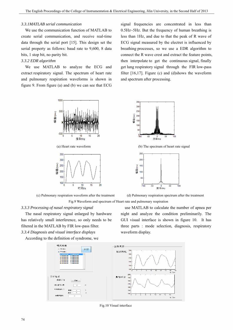
期 The English Proceedings of the College of Instrumentation & Electrical Engineering, Jilin University, in the Second Half of 2013
74
3.3.1MATLAB serial communication We use the communication function of MATLAB to
create serial communication, and receive real-time data through the serial port [15]. This design set the serial property as follows: baud rate to 9,600, 8 data bits, 1 stop bit, no parity bit. 3.3.2 EDR algorithm
We use MATLAB to analyze the ECG and extract respiratory signal. The spectrum of heart rate and pulmonary respiration waveforms is shown in figure 9. From figure (a) and (b) we can see that ECG
signal frequencies are concentrated in less than 0.5Hz~5Hz. But the frequency of human breathing is less than 1Hz, and due to that the peak of R wave of ECG signal measured by the electret is influenced by breathing processes, so we use a EDR algorithm to connect the R wave crest and extract the feature points, then interpolate to get the continuous signal, finally get lung respiratory signal through the FIR low-pass filter [16,17]. Figure (c) and (d)shows the waveform and spectrum after processing.
(a) Heart rate waveform (b) The spectrum of heart rate signal
(c) Pulmonary respiration waveform after the treatment (d) Pulmonary respiration spectrum after the treatment
Fig.9 Waveform and spectrum of Heart rate and pulmonary respiration
3.3.3 Processing of nasal respiratory signal The nasal respiratory signal enlarged by hardware
has relatively small interference, so only needs to be filtered in the MATLAB by FIR low-pass filter. 3.3.4 Diagnosis and visual interface displays
According to the definition of syndrome, we
use MATLAB to calculate the number of apnea per night and analyze the condition preliminarily. The GUI visual interface is shown in figure 10. It has three parts : mode selection, diagnosis, respiratory waveform display.
Fig.10 Visual interface
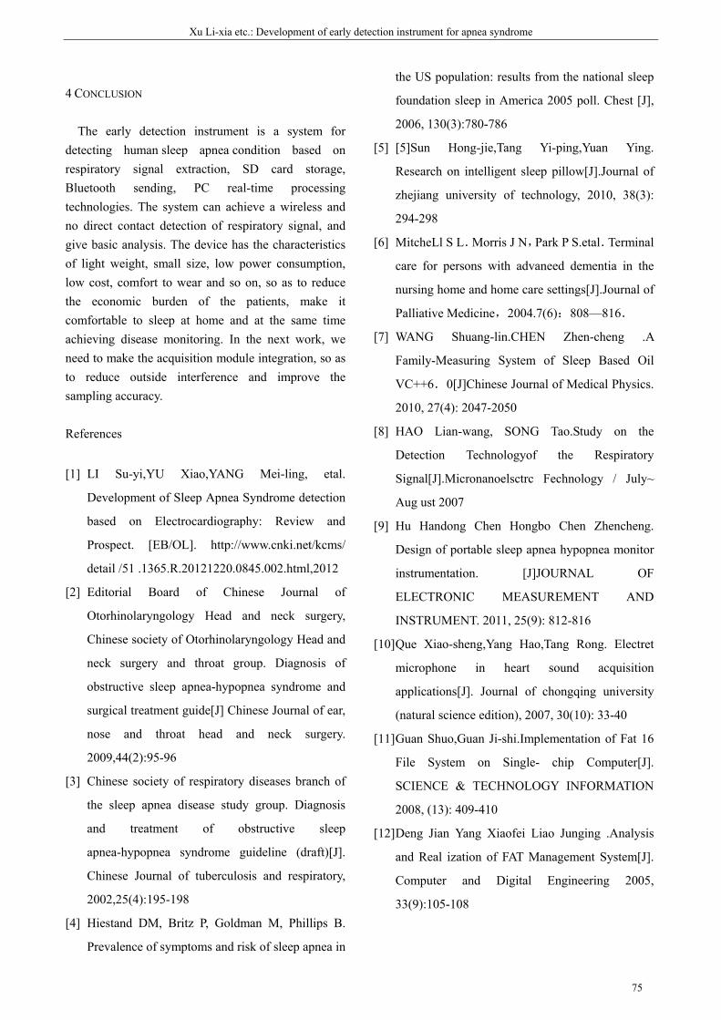
Xu Li-xia etc.: Development of early detection instrument for apnea syndrome
75
4 CONCLUSION
The early detection instrument is a system for detecting human sleep apnea condition based on respiratory signal extraction, SD card storage, Bluetooth sending, PC real-time processing technologies. The system can achieve a wireless and no direct contact detection of respiratory signal, and give basic analysis. The device has the characteristics of light weight, small size, low power consumption, low cost, comfort to wear and so on, so as to reduce the economic burden of the patients, make it comfortable to sleep at home and at the same time achieving disease monitoring. In the next work, we need to make the acquisition module integration, so as to reduce outside interference and improve the sampling accuracy.
References
[1] LI Su-yi,YU Xiao,YANG Mei-ling, etal.
Development of Sleep Apnea Syndrome detection
based on Electrocardiography: Review and
Prospect. [EB/OL]. http://www.cnki.net/kcms/
detail /51 .1365.R.20121220.0845.002.html,2012
[2] Editorial Board of Chinese Journal of
Otorhinolaryngology Head and neck surgery,
Chinese society of Otorhinolaryngology Head and
neck surgery and throat group. Diagnosis of
obstructive sleep apnea-hypopnea syndrome and
surgical treatment guide[J] Chinese Journal of ear,
nose and throat head and neck surgery.
2009,44(2):95-96
[3] Chinese society of respiratory diseases branch of
the sleep apnea disease study group. Diagnosis
and treatment of obstructive sleep
apnea-hypopnea syndrome guideline (draft)[J].
Chinese Journal of tuberculosis and respiratory,
2002,25(4):195-198
[4] Hiestand DM, Britz P, Goldman M, Phillips B.
Prevalence of symptoms and risk of sleep apnea in
the US population: results from the national sleep
foundation sleep in America 2005 poll. Chest [J],
2006, 130(3):780-786
[5] [5]Sun Hong-jie,Tang Yi-ping,Yuan Ying.
Research on intelligent sleep pillow[J].Journal of
zhejiang university of technology, 2010, 38(3):
294-298
[6] MitcheLl S L.Morris J N,Park P S.etal.Terminal
care for persons with advaneed dementia in the
nursing home and home care settings[J].Journal of
Palliative Medicine,2004.7(6):808—816.
[7] WANG Shuang-lin.CHEN Zhen-cheng .A
Family-Measuring System of Sleep Based Oil
VC++6.0[J]Chinese Journal of Medical Physics.
2010, 27(4): 2047-2050
[8] HAO Lian-wang, SONG Tao.Study on the
Detection Technologyof the Respiratory
Signal[J].Micronanoelsctrc Fechnology / July~
Aug ust 2007
[9] Hu Handong Chen Hongbo Chen Zhencheng.
Design of portable sleep apnea hypopnea monitor
instrumentation. [J]JOURNAL OF
ELECTRONIC MEASUREMENT AND
INSTRUMENT. 2011, 25(9): 812-816
[10] Que Xiao-sheng,Yang Hao,Tang Rong. Electret
microphone in heart sound acquisition
applications[J]. Journal of chongqing university
(natural science edition), 2007, 30(10): 33-40
[11] Guan Shuo,Guan Ji-shi.Implementation of Fat 16
File System on Single- chip Computer[J].
SCIENCE & TECHNOLOGY INFORMATION
2008, (13): 409-410
[12] Deng Jian Yang Xiaofei Liao Junging .Analysis
and Real ization of FAT Management System[J].
Computer and Digital Engineering 2005,
33(9):105-108

期 The English Proceedings of the College of Instrumentation & Electrical Engineering, Jilin University, in the Second Half of 2013
76
[13] Cai Jing. A Wearable ECG Monitoring System
Based on FAT16 File Format[D].jlin university.
2010
[14] Luo Zhi-da,Yu Xue-fei,Peng Da-ming. Medical
equipment based on Bluetooth technology design
and implementation of communication interface
between[J]. Medical and health care
equipment .2010, 31(2): 28-31
[15] Gu Xue-qiao,Cao Yun,Xu Yan lin. Serial
communication based on MATLAB and
filtering[J]. Instrumentation Technology, 2010, (8):
17-19
[16] Zhao Su-wen,Jia Lei-lei,Lu Wang. Based on the
discussion of extracting respiratory signal from
ECG[J]. Journal of guilin aerospace industry
college, 2012, (65): 20-24
[17] Li Qiang,Zhao w\Wei. MATLAB Data processing
and application[M].beijing: National Defence
Industry Press ,20
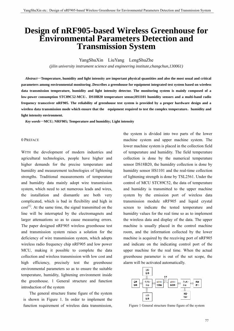
YangShuXin etc.: Design of nRF905-based Wireless Greenhouse for Environmental Parameters Detection and Transmission System
77
Design of nRF905-based Wireless Greenhouse for Environmental Parameters Detection and
Transmission System
YangShuXin LiuYang LengShuZhe (jilin university instrument science and engineering institute,changchun,130061)
Abstract—Temperature, humidity and light intensity are important physical quantities and also the most usual and critical
parameters among environmental monitoring .Describes a greenhouse for equipment integrated test system based on wireless
data transmission temperature, humidity and light intensity detector. The monitoring system is mainly composed of a
low-power consumption STC89C52-MCU、DS18B20 temperature sensor,HS1101 humidity sensors and a multi-band radio
frequency transceiver nRF905. The reliability of greenhouse test system is provided by a proper hardware design and a
wireless data transmission mode which ensure that the equipment required to test the complex temperature,humidity and
light intensity environment.
Key words—MCU; NRF905; Temperature and humidity; Light intensity
0 PREFACE
WITH the development of modern industries and agricultural technologies, people have higher and higher demands for the precise temperature and humidity and measurement technologies of lightening strengths. Traditional measurements of temperature and humidity data mainly adopt wire transmission system, which need to set numerous leads and wires, the installation and dismantle are both very complicated, which is bad in flexibility and high in cost[1]. At the same time, the signal transmitted on the line will be interrupted by the electromagnets and larger attenuations so as to cause measuring errors. The paper designed nRF905 wireless greenhouse test and transmission system raises a solution for the deficiency of wire transmission system, which adopts wireless radio frequency chip nRF905 and low power MCU, making it possible to complete the data collection and wireless transmission with low cost and high efficiency, precisely test the greenhouse environmental parameters so as to ensure the suitable temperature, humidity, lightening environment inside the greenhouse. 1 General structure and function introduction of the system
The general structure frame figure of the system is shown in Figure 1. In order to implement the function requirement of wireless data transmission,
the system is divided into two parts of the lower machine system and upper machine system. The lower machine system is placed in the collection field of temperature and humidity. The field temperature collection is done by the numerical temperature sensor DS18B20, the humidity collection is done by humidity sensor HS1101 and the real-time collection of lightening strength is done by TSL2561. Under the control of MCU STC89C52, the data of temperature and humidity is transmitted to the upper machine system by the emission port of wireless data transmission module nRF905 and liquid crystal screen to indicate the tested temperature and humidity values for the real time so as to implement the wireless data and display of the data. The upper machine is usually placed in the control machine room, and the information collected by the lower machine is acquired by the receiving port of nRF905 and indicate on the indicating control port of the upper machine for the real time. When the actual greenhouse parameter is out of the set scope, the alarm will be activated automatically.
Figure 1 General structure frame figure of the system
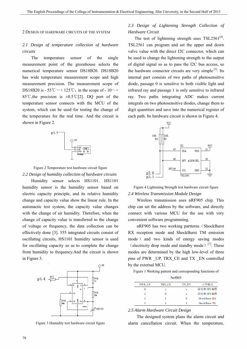
期 The English Proceedings of the College of Instrumentation & Electrical Engineering, Jilin University, in the Second Half of 2013
78
2 DESIGN OF HARDWARE CIRCUITS OF THE SYSTEM
2.1 Design of temperature collection of hardware circuits
The temperature sensor of the single measurement point of the greenhouse selects the numerical temperature sensor DS18B20. DS18B20 has wide temperature measurement scope and high measurement precision. The measurement scope of DS18B20 is - 55~+ 125;in the scope of - 10~+ 85 ,the precision is ±0.5 [2]. DQ port of the
temperature sensor connects with the MCU of the system, which can be used for testing the change of the temperature for the real time. And the circuit is shown in Figure 2.
Figure 2 Temperature test hardware circuit figure
2.2 Design of humidity collection of hardware circuits Humidity sensor selects HS1101. HS1101
humidity sensor is the humidity sensor based on electric capacity principle, and its relative humidity change and capacity value show the linear rule. In the automactic test system, the capacity value changes with the change of air humidity. Therefore, when the change of capacity value is transferred to the change of voltage or frequency, the data collection can be effectively done [3]. 555 integrated circuits consist of oscillating circuits, HS1101 humidity sensor is used for oscillating capacity so as to complete the change from humidity to frequency.And the circuit is shown in Figure 3.
Figure 3 Humidity test hardware circuit figure
2.3 Design of Lightening Strength Collection of Hardware Circuit
The test of lightening strength uses TSL2561[4]. TSL2561 can program and set the upper and down valve value with the direct I2C connector, which can be used to change the lightening strength to the output of digital signal so as to pass the I2C bus access, so the hardware connector circuits are very simple [5]. Its internal part consists of two paths of photosensitive diode, passage 0 is sensitive to both visible light and infrared ray and passage 1 is only sensitive to infrared ray. Two paths integrating ADC makes current integrals on two photosensitive diodes, change them to digit quantities and save into the numerical register of each path. Its hardware circuit is shown in Figure 4.
Figure 4 Lightening Strength test hardware circuit figure
2.4 Wireless Transmission Module Design Wireless transmission uses nRF905 chip. This
chip can set the address by the software, and directly connect with various MCU for the use with very convenient software programming.
nRF905 has two working partterns(ShockBurst RX reception mode and ShockBurst TM emission mode ) and two kinds of energy saving modes (electricity drop mode and standby mode)[7]. These modes are determined by the high low-level of three pins of PWR _UP, TRX_CE and TX _EN controlled by the external MCU.
Figure 1 Working pattern and corresponding functions of
Nrf905
2.5 Alarm Hardware Circuit Design
The designed system plans the alarm circuit and alarm cancellation circuit. When the temperature,
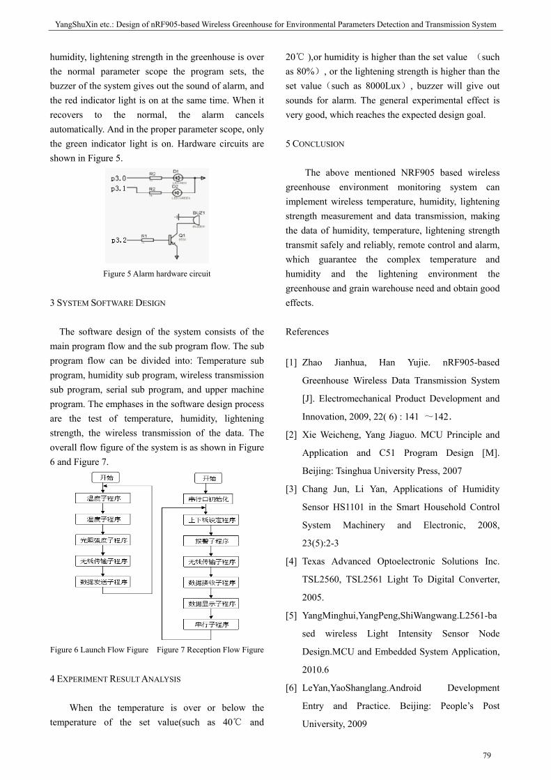
YangShuXin etc.: Design of nRF905-based Wireless Greenhouse for Environmental Parameters Detection and Transmission System
79
humidity, lightening strength in the greenhouse is over the normal parameter scope the program sets, the buzzer of the system gives out the sound of alarm, and the red indicator light is on at the same time. When it recovers to the normal, the alarm cancels automatically. And in the proper parameter scope, only the green indicator light is on. Hardware circuits are shown in Figure 5.
Figure 5 Alarm hardware circuit
3 SYSTEM SOFTWARE DESIGN
The software design of the system consists of the main program flow and the sub program flow. The sub program flow can be divided into: Temperature sub program, humidity sub program, wireless transmission sub program, serial sub program, and upper machine program. The emphases in the software design process are the test of temperature, humidity, lightening strength, the wireless transmission of the data. The overall flow figure of the system is as shown in Figure 6 and Figure 7.
Figure 6 Launch Flow Figure Figure 7 Reception Flow Figure
4 EXPERIMENT RESULT ANALYSIS
When the temperature is over or below the temperature of the set value(such as 40 and
20 ),or humidity is higher than the set value (such as 80%), or the lightening strength is higher than the set value(such as 8000Lux), buzzer will give out sounds for alarm. The general experimental effect is very good, which reaches the expected design goal.
5 CONCLUSION
The above mentioned NRF905 based wireless greenhouse environment monitoring system can implement wireless temperature, humidity, lightening strength measurement and data transmission, making the data of humidity, temperature, lightening strength transmit safely and reliably, remote control and alarm, which guarantee the complex temperature and humidity and the lightening environment the greenhouse and grain warehouse need and obtain good effects.
References
[1] Zhao Jianhua, Han Yujie. nRF905-based
Greenhouse Wireless Data Transmission System
[J]. Electromechanical Product Development and
Innovation, 2009, 22( 6) : 141 ~142.
[2] Xie Weicheng, Yang Jiaguo. MCU Principle and
Application and C51 Program Design [M].
Beijing: Tsinghua University Press, 2007
[3] Chang Jun, Li Yan, Applications of Humidity
Sensor HS1101 in the Smart Household Control
System Machinery and Electronic, 2008,
23(5):2-3
[4] Texas Advanced Optoelectronic Solutions Inc.
TSL2560, TSL2561 Light To Digital Converter,
2005.
[5] YangMinghui,YangPeng,ShiWangwang.L2561-ba
sed wireless Light Intensity Sensor Node
Design.MCU and Embedded System Application,
2010.6
[6] LeYan,YaoShanglang.Android Development
Entry and Practice. Beijing: People’s Post
University, 2009

期 The English Proceedings of the College of Instrumentation & Electrical Engineering, Jilin University, in the Second Half of 2013
80
[7] Guo Hongzhi. Android Application Development
Context[M].Beijing: Electronic Industry Press,
2010
[8] Jiang Yan, Xu Yan. Design of DS18B20-based
Multipoint Circuit Measuring Instrument [J]
Journal of Daqing Normal University,
2009,29(6):20-22
[9] Li Guoping, Wu Haiyan. Application Research of
the Implementation of C51 on I2C Bus Fujian
Computer, 2006(9) : 168, 182.

Wu Jindi etc.: Wireless multi-point temperature and humidity detection system design based on nRF24L01
81
Wireless multi-point temperature and humidity detection system design based on nRF24L01
Wu Jindi Song Qihan Zhao Xiaoyi
(College of instrumentation and electrical Engineering Jilin University,Changchun.China) Abstract—This project proposes a design of environmental temperature and humidity monitoring system based on wireless
sensor Nrf24l01.The scheme is based on nRF24L01 to design a wireless temperature acquisition system. The system adopts
low power, high performance microcontroller AT89C51 and the temperature and humidity sensor DHT11 to constitute a
multiple point, real-time monitoring system of temperature and humidity, finally completes the function configuration,
display and alarm in the PC machine. The system is easy to use, very easy to expand, can be widely used in various industrial
production and aquaculture.
Key words—Wireless data transmission;nRF24L01;DHT11; A multi data acquisition; PC real-time monitoring;
0 INTRODUCTION
In today's industrial and agricultural production, required temperature and humidity acquisition of more and more occasions, accurately and easily measure the temperature becomes critical. Traditional wired temperature measurement method sexist complex wiring, easy to aging lines,line fault is difficult to trouble shoot, equipment relocation and other issues to bere-wiring. Especially in the wired net work is not open or because of site restrictions and inconvenience of environmental factors in the case set up lines to temperature and humidity data acquisition brought a lot of trouble. To monitor the real-time temperature and humidity data, you must use wireless transmission for data collection, transmission,reception and wireless data collected tobe processed through the host computer to control and monitor the operation of equipment and reduce unnecessary line equipment expenses.
1 SYSTEM COMPONENTS
This design of multi-node wireless temperature and humidity monitoring system monitoring and control system, the microcontroller and RF
communications systems combine master and slave system consists of two parts, the slave is responsible for detecting temperature and humidity, and the
collected data sent through the RF system host, the host receives a signal sent from the slave, and the PC via the serial port to communicate, log data. While setting the alarm data via PC upper and lower limits.
2 CORE HARD WARE MODULE DESIGN
2.1 Temperature and humidity acquisition circuit design
Ina multi-node acquisition module temperature and humidity, we mainly use DHT11 temperature and humidity sensor as a core component into Line design.
Sensor module using DHT11 digital temperature and humidity sensors. This is a digital signal output with a calibrated temperature and humidity combined sensors, application-specific temperature and humidity sensor technology and digital modules capture technology, with long-term stability and high reliability. DHTl l sensor using single-wire serial interface, the application of simple and quick, the signal transmission distance up to 20 m or more. When the cable length is shorter than 20m should be used when 5kΩ pullup resistor, more than 20m should be based on the situation using the appropriate pull-up resistors. The temperature and humidity sensors with small size, low power consumption, fast response, anti-interference ability and cost advantages. Detailed circuit diagram shown in Figure 1.
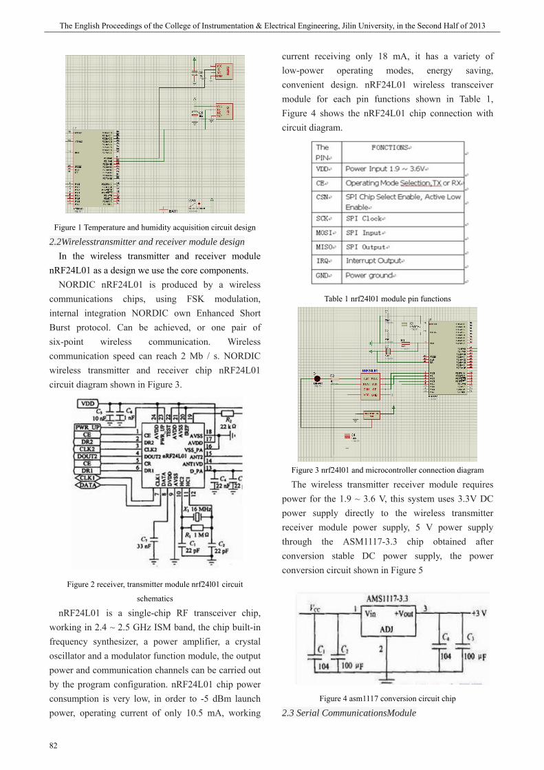
期 The English Proceedings of the College of Instrumentation & Electrical Engineering, Jilin University, in the Second Half of 2013
82
Figure 1 Temperature and humidity acquisition circuit design
2.2Wirelesstransmitter and receiver module design In the wireless transmitter and receiver module
nRF24L01 as a design we use the core components. NORDIC nRF24L01 is produced by a wireless
communications chips, using FSK modulation, internal integration NORDIC own Enhanced Short Burst protocol. Can be achieved, or one pair of six-point wireless communication. Wireless communication speed can reach 2 Mb / s. NORDIC wireless transmitter and receiver chip nRF24L01 circuit diagram shown in Figure 3.
Figure 2 receiver, transmitter module nrf24l01 circuit
schematics
nRF24L01 is a single-chip RF transceiver chip, working in 2.4 ~ 2.5 GHz ISM band, the chip built-in frequency synthesizer, a power amplifier, a crystal oscillator and a modulator function module, the output power and communication channels can be carried out by the program configuration. nRF24L01 chip power consumption is very low, in order to -5 dBm launch power, operating current of only 10.5 mA, working
current receiving only 18 mA, it has a variety of low-power operating modes, energy saving, convenient design. nRF24L01 wireless transceiver module for each pin functions shown in Table 1, Figure 4 shows the nRF24L01 chip connection with circuit diagram.
Table 1 nrf24l01 module pin functions
Figure 3 nrf24l01 and microcontroller connection diagram
The wireless transmitter receiver module requires power for the 1.9 ~ 3.6 V, this system uses 3.3V DC power supply directly to the wireless transmitter receiver module power supply, 5 V power supply through the ASM1117-3.3 chip obtained after conversion stable DC power supply, the power conversion circuit shown in Figure 5
Figure 4 asm1117 conversion circuit chip
2.3 Serial CommunicationsModule

Wu Jindi etc.: Wireless multi-point temperature and humidity detection system design based on nRF24L01
83
In serial communication module, we use the core member is PL2303.
Prolific PL2303 is produced by a highly integrated RS232-USB interface converter that provides a full-duplex asynchronous RS232 serial communication device connected to the USB function interface convenient solution. The device built-in USB function controller, USB transceiver, oscillator, and with full modem control signals UART, just add a few capacitors can achieve USB signals and RS232 signal conversion, can be easily embedded into handheld devices. The device as bidirectional USB/RS232 converter, one USB data received from the host and converts RS232 send message stream format peripherals; hand to receive data from RS232 peripherals into USB data format sent back to the host. All these tasks done automatically by the device, developers need to consider firmware design.
By using the USB block transfer mode, the use of large data buffers and automatic flow control, PL2303HX able to achieve higher throughput than traditional UART (Universal Asynchronous starting device) ports, up to 115200 bps baud rate can be used for higher performance be used. System serial communication module connection diagram in Figure 6 below.
Figure 5 Serial Port Module Design
3 SOFTWARE DESIGN
3.1lower computer software The system uses the C programming language,shall
be determined according to the design requirements of the task the complete structure of the system program,as modular programming method,the task is divided into relatively independent functional modules,each module features a clear,chronological and relationships,system software design can be
divided into several parts, the first is the underlying driver of each module to write, and then the system on-line debugging, and finally the preparation of PC system program.Control and management of the main program is the core of the system is powered on,the first initialization,the system begins normal operation, and then carry out the temperature and humidity monitoring and processing operations. 3.2PC software design
System complete function position function displays the serial number, indicating whether the serial port has been successfully opened;Meanwhile, the PC and the next crew to simultaneous display of temperature and humidity of each node in the range of temperature and humidity over warning after the buzzer control slave alarm.
PC software is available on the PCthroughVC6.0 prepared, mainly on the MSCommcontrol and CserialPort class operation.
The first is the serial port settings.The system uses the CSERIALPORT class initialization function InitPort (this, nport, nbtl, 'N', 8,1, m_dwCommEvents, 512).Which nport for the serial number, nbtl baud rate, you can use the serial port settings dialog baud serial number and two combo boxes initialization function were obtained in nport and nbtl.
Followed by the upper and lower limit son the temperature and humidity settings.Available CSERIALPORT class start serial monitoring process function Start Monitoring,send the string functions Write To Port and close the serial port processes Stop Monitoring for upper and lower temperature settings, the information is sent to the serial port through these functions,the micro controller receives the datafromRS232,compared with its own temperature, and then make the appropriate treatment.
4 EXPERIMENTAL RESULTS
DHT11 digital temperature and humidity sensor uses a single-wire bidirectional serial interface technology, a communication time is about 4ms, the data sub-fractional and integer part, a complete data transfer is 40bit, MSB first. Ie 8bit Humidity Humidity decimal integer data +8 bit temperature data +8 bit decimal integer data + 8bit temperature data + 8bit checksum, which is equal to the calibration data of

期 The English Proceedings of the College of Instrumentation & Electrical Engineering, Jilin University, in the Second Half of 2013
84
four 8bit data and findings of the last eight. For example: read data as: humidity: 36.50%; temperature of 22.80 , then the corresponding 40bit data: 0010 0100,0011 0010,0001 0110,0101 0000,1011 1100, tested, no increase in the transmitting and receiving antenna module case, the wireless transmitting and receiving module, in most cases the data transmission distance of about 200 m in the error rate is less than 3%, the transmitter first transmit power, receiver sensitivity receiver factors that may affect the transmission distance, if separate antennas , will greatly increase the transmission distance. In addition, the debugging process, oscillation resistor must match, otherwise the receiver can not receive even the distance becomes shorter.
5 CONCLUSION
Through unremitting efforts, and finally completed the wireless multi-point temperature and humidity detection system of the preliminary work, namely the overall hardware connection. As well as temperature and humidity control part, PC interface debugging have been completed. According to our design of the control approach can achieve the collection and transmission of temperature and humidity as well as displayed on the PC screen, you can display the current temperature and humidity changes; the buttons, sensors and other input signals into the microcontroller, and then based on the information obtained upward position machine signals the control PC interface real-time display of temperature and humidity, reached a temperature and humidity testing purposes. At the same time when the air humidity below 20% or above 80% of the time the buzzer will alarm automatically. On the basis of these. Free to the control system through the key switch.
References
[1] Zhao Zhongbiao. NRF401in the greenhouse
control system application research[J].Industrial
control computer,200821(3)
[2] Xiqiang.Greenhouse monitoring control
system[D]. Beijing:China Agricultural University,
2005
[3] Li Shanjun,Zhang Yanlin,Ai Ping,Zhai Hong;
Greenhouse Environment Control Technology
Application and Development Trend[J];
Agricultural Engineering Technology(Greenhouse
Horticulture)200802
[4] HeQiao.Micro controller Theory and Applications.
China Railway Press,2006.5
[5] Yang Suxing.Analog Electronics concise tutorials.
Higher Education Press,2008.4
[6] Tan Haoqiang. C programming.Tsinghua
University Press.2007.5
[7] Li Wei, Duan Cuifang, Hua Weijuan;greenhouse
monitoring systemat home and abroad
development status and trends[J];Chinese fruits
and vegetables;201006
[8] Zheng Wengang,ZHAO Chunjiang,Wang Jihua;
Greenhouse Intelligent Control Research
Progress[J];Agriculture Network Information;
200402
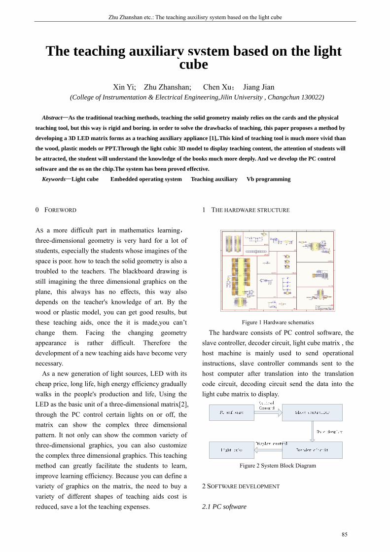
Zhu Zhanshan etc.: The teaching auxilisry system based on the light cube
85
The teaching auxiliary system based on the light cube
Xin Yi; Zhu Zhanshan; Chen Xu; Jiang Jian
(College of Instrumentation & Electrical Engineering,Jilin University , Changchun 130022)
Abstract—As the traditional teaching methods, teaching the solid geometry mainly relies on the cards and the physical
teaching tool, but this way is rigid and boring. in order to solve the drawbacks of teaching, this paper proposes a method by
developing a 3D LED matrix forms as a teaching auxiliary appliance [1],.This kind of teaching tool is much more vivid than
the wood, plastic models or PPT.Through the light cubic 3D model to display teaching content, the attention of students will
be attracted, the student will understand the knowledge of the books much more deeply. And we develop the PC control
software and the os on the chip.The system has been proved effective.
Keywords—Light cube Embedded operating system Teaching auxiliary Vb programming
0 FOREWORD
AS a more difficult part in mathematics learning, three-dimensional geometry is very hard for a lot of students, especially the students whose imagines of the space is poor. how to teach the solid geometry is also a troubled to the teachers. The blackboard drawing is still imagining the three dimensional graphics on the plane, this always has no effects, this way also depends on the teacher's knowledge of art. By the wood or plastic model, you can get good results, but these teaching aids, once the it is made,you can’t change them. Facing the changing geometry appearance is rather difficult. Therefore the development of a new teaching aids have become very necessary.
As a new generation of light sources, LED with its cheap price, long life, high energy efficiency gradually walks in the people's production and life, Using the LED as the basic unit of a three-dimensional matrix[2], through the PC control certain lights on or off, the matrix can show the complex three dimensional pattern. It not only can show the common variety of three-dimensional graphics, you can also customize the complex three dimensional graphics. This teaching method can greatly facilitate the students to learn, improve learning efficiency. Because you can define a variety of graphics on the matrix, the need to buy a variety of different shapes of teaching aids cost is reduced, save a lot the teaching expenses.
1 THE HARDWARE STRUCTURE
Figure 1 Hardware schematics
The hardware consists of PC control software, the slave controller, decoder circuit, light cube matrix , the host machine is mainly used to send operational instructions, slave controller commands sent to the host computer after translation into the translation code circuit, decoding circuit send the data into the light cube matrix to display.
Figure 2 System Block Diagram
2 SOFTWARE DEVELOPMENT
2.1 PC software
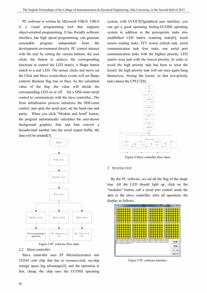
期 The English Proceedings of the College of Instrumentation & Electrical Engineering, Jilin University, in the Second Half of 2013
86
PC software is written by Microsoft VB6.0. VB6.0 is a visual programming tool that supports object-oriented programming. It has friendly software interface, has high speed programming, can generate executable program independent from the development environment directly. PC control interact with the user by setting the various buttons, the user clicks the button to achieve the corresponding functions to control the LED matrix. a Shape button match to a real LED. The mouse clicks and move set the Click and Move events,these events will set Shape controls Boolean flag true or flase. by the calculated value of the flag ,the value will decide the corresponding LED on or off. Set a MSComm serial control to communicate with the slave controller., The form initialization process initializes the MSComm control, and open the serial port, set the baud rate and parity. When you click "Modulo and Send" button, the program automatically calculates the user-drawn background graphics font and font convert a hexadecimal number into the serial output buffer, the data will be sended[3].
Begin
Form inti
Display init
Port init
Button click Mouse click Mouse move
The Correspondingopperation
The shape on or off
The line on or off
Figure 3 PC software flow chart
2.2 Slave controller Slave controller uses ST Microelectronics stm
32f103 zet6 chip that has io resource-rich, on-chip storage space big advantage[4], and the operation is fast, cheap, the chip uses the UCOSII operating
system, with UCGUI[5]graphical user interface, you can get a good operating feeling.UCOSII operating system in addition to the prerequisite tasks also established LED matrix scanning tasks[6], touch screen reading tasks, TFT screen refresh task, serial communication task four tasks, one serial port communication tasks with the highest priority, LED matrix scan task with the lowest priority. In order to avoid the high priority task has been to seize the kernel, the high priority task will run once again hang themselves, freeing the kernel, so that low-priority task canuse the CPU[7][8].
Figure 4 Slave controller flow chart
3 SYSTEM TEST
By the PC software ,we set all the flag of the shape true. All the LED should light up, click on the "modulus" button, call a serial port control sends the data to the slave controller, after all operation, the display as follows.
Figure 5 PC software interface

Zhu Zhanshan etc.: The teaching auxilisry system based on the light cube
87
Figure 6 Physical presentation charts
4 CONCLUSION
PC control via light cube matrix display can make a complex geometry, and has a good display, but the resolution is too complex geometry constraints received, the display is not very good, the PC used LED is mapped to a physical host machine control method, which requires the use of a person with a good spatial imagination. How to allow users to draw directly on the host computer 3D graphics, as well as to improve the display resolution will need to be further addressed.
References
[1] Kang Zhiqiang, Wang Jia, Tang Yongming.
FPGA-based 3D Light Cube Design [J].
Electronic devices .2012.12,6.
[2] Kuo Yuan Fen. Semiconductor LED lighting
industry and technology status [A]. 2011 Green
Lighting Technology Conference and Scientific
Development and the Fourth Japan-Korea
Conference presentations lighting Proceedings [C].
2011
[3] hook Huilan, Liu Chao STM32-based minimum
system and serial port communication [J].
Industrial control computer,
[4] Mombo Yu. STM32 Study Notes [M]. Beijing:
Beijing University of Aeronautics and
Astronautics Press, 2012.
[5] Liu Bo Wen, SUN Yan. Embedded real-time
operating system μC/OS- Ⅱ classic example -
Based on the STM32 processor [M]. Beijing:
Beijing University of Aeronautics and
Astronautics Press,2012:138-144
[6] Dai Jun Jian, ZHANG Chuan-sheng.
STM32-based human-computer interface design
and implementation [J]. Changchun University of
Technology (Natural Science Edition), 2012,33
(6) :672-675
[7] Wang Zhongkai, Zhao Lei. UC / OS-II task
scheduling. Shandong University of Technology
(Natural Science Edition) .2009,23 (2) :30-35
[8] Wang Xinzheng, Cheng Xiaohui, Zhou Huamao.
RTOS task scheduling strategy research and
design. [J] embedded operating system
applications .2007,23 (4-2) :57-5

期 The English Proceedings of the College of Instrumentation & Electrical Engineering, Jilin University, in the Second Half of 2013
88
Intelligent alarm system based on MMS
Zhang Yixuan ,Zhou Xianze, Liu Yan (Jilin University electrical engineering and automation, Changchun, 130001)
Abstract—This article introduces an intelligent alarm system based on used cell phones, and mainly describes the
composition and structure of the system as well as the hardware and software design in detail. This system uses old cell
phones to send and receive messages, in order to supervise and control our home safety . We use infrared sensors to collect
information, and use network information technology to get the accurate warning . When the owner receives the alarm
information, he can know the situation at the scene ,so he can call the police in time to ensure domestic safety and security.
The structure of the system is simple, and it is not only easy to install ,but also convenient to operate.
Key words—MMS alarm; intelligence security; home safety; used cell phones; single-chip microcomputer
1.INTRODUCTION
WITH the increase of urban floating population, city social security situation is getting worse. Daytime shelter, night-time warehouses store may be in a State of no one left behind, which provides opportunities for criminals. At present, most residential burglar use anti-theft iron fence, which is not beautiful and hard to escape. Some high-end home alarm system cannot be accepted by consumers because of its expensive price ,therefore its promotion is limited. [1] Considering the family need, our team designed an intelligent burglar alarm system based on MMS, it is practical and stable,it can effectively prevent illegal theft of vandalism.
In our country, home security alarm systems have become the basis for achieving safety management in intelligent community. Intelligent alarm is part of the family. [13] the alarm equipment is mainly in two areas develop faster, development of the detector and the detector on the one hand, on the one hand is the development of remote alarm systems. Detector has emerged mainly in the development of three different passive infrared, ultrasonic and microwave detection technologies, different types of detectors are expected to emerge. Has emerged mainly in the development of remote alarm system wired alarm system, wireless alarm system, alarm and protection networks. At the same time, a lot of burglar alarm systems introduces FPGA technologies. In addition, along with the extensive video surveillance system, centralized
network monitoring demands more and more, especially the green city construction and telecommunications operators such as Netcom's involvement, making further accelerated the pace of the network.
In recent years, the security industry develop in IT very fast. While domestic security technology development, smart security penetration but my relative abroad, still has a long way to go. Abroad has successfully developed several sets of sophisticated weapons in security systems. For example, the United States C&K 2,300 series and "MONITOR" monitor software, United States ADEMCO 4,110 series burglar alarm systems, domestic production of such products as Kang Bite electronic technology Research Institute CPT-302 paging alarm system. Such flexible system using microcomputer software, CorelDraw, management is simple, convenient, and graphics by the rich features, such as monitoring software can monitor dozens of even hundreds of controlled extensions, performance/price ratio is higher. China's smaller systems, do not form a series and the commercialization of products, only some simple monitoring system of microcomputer software, such as Kang Bite electronic technology Research Institute CPT-302 paging alarm system, etc.
With the rapid economic development of society and the continuous improvement of people's living standard, people need an intelligent home security alarm system. Home monitoring system in the past, due to poor reliability, single function or expensive and hard to spread. [10] with the development of
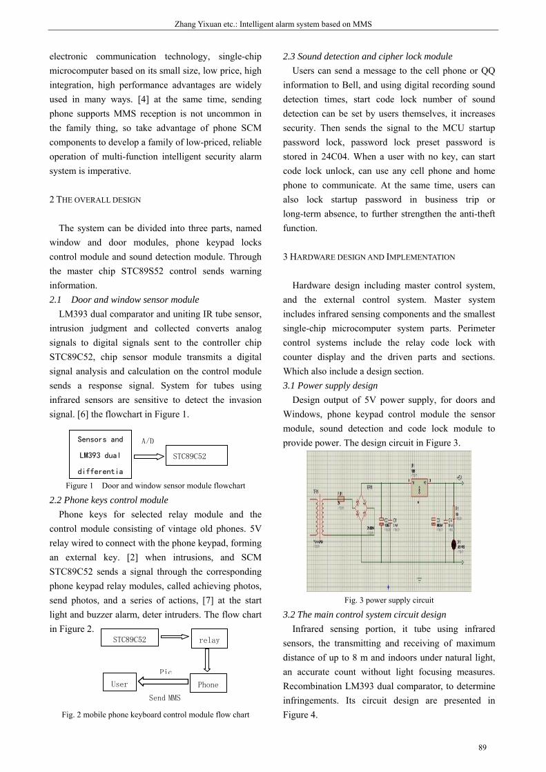
Zhang Yixuan etc.: Intelligent alarm system based on MMS
89
electronic communication technology, single-chip microcomputer based on its small size, low price, high integration, high performance advantages are widely used in many ways. [4] at the same time, sending phone supports MMS reception is not uncommon in the family thing, so take advantage of phone SCM components to develop a family of low-priced, reliable operation of multi-function intelligent security alarm system is imperative.
2 THE OVERALL DESIGN
The system can be divided into three parts, named window and door modules, phone keypad locks control module and sound detection module. Through the master chip STC89S52 control sends warning information. 2.1 Door and window sensor module
LM393 dual comparator and uniting IR tube sensor, intrusion judgment and collected converts analog signals to digital signals sent to the controller chip STC89C52, chip sensor module transmits a digital signal analysis and calculation on the control module sends a response signal. System for tubes using infrared sensors are sensitive to detect the invasion signal. [6] the flowchart in Figure 1.
Figure 1 Door and window sensor module flowchart
2.2 Phone keys control module Phone keys for selected relay module and the
control module consisting of vintage old phones. 5V relay wired to connect with the phone keypad, forming an external key. [2] when intrusions, and SCM STC89C52 sends a signal through the corresponding phone keypad relay modules, called achieving photos, send photos, and a series of actions, [7] at the start light and buzzer alarm, deter intruders. The flow chart in Figure 2.
Fig. 2 mobile phone keyboard control module flow chart
2.3 Sound detection and cipher lock module Users can send a message to the cell phone or QQ
information to Bell, and using digital recording sound detection times, start code lock number of sound detection can be set by users themselves, it increases security. Then sends the signal to the MCU startup password lock, password lock preset password is stored in 24C04. When a user with no key, can start code lock unlock, can use any cell phone and home phone to communicate. At the same time, users can also lock startup password in business trip or long-term absence, to further strengthen the anti-theft function.
3 HARDWARE DESIGN AND IMPLEMENTATION
Hardware design including master control system, and the external control system. Master system includes infrared sensing components and the smallest single-chip microcomputer system parts. Perimeter control systems include the relay code lock with counter display and the driven parts and sections. Which also include a design section. 3.1 Power supply design
Design output of 5V power supply, for doors and Windows, phone keypad control module the sensor module, sound detection and code lock module to provide power. The design circuit in Figure 3.
Fig. 3 power supply circuit
3.2 The main control system circuit design Infrared sensing portion, it tube using infrared
sensors, the transmitting and receiving of maximum distance of up to 8 m and indoors under natural light, an accurate count without light focusing measures. Recombination LM393 dual comparator, to determine infringements. Its circuit design are presented in Figure 4.
Sensors and
LM393 dual
differentia
A/D
STC89C52
STC89C52 relay
Phone User
Pic
Send MMS
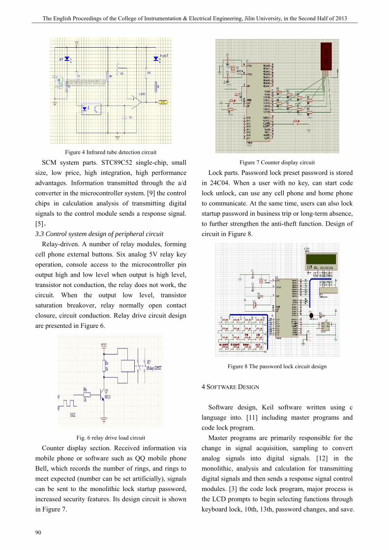
期 The English Proceedings of the College of Instrumentation & Electrical Engineering, Jilin University, in the Second Half of 2013
90
Figure 4 Infrared tube detection circuit
SCM system parts. STC89C52 single-chip, small size, low price, high integration, high performance advantages. Information transmitted through the a/d converter in the microcontroller system. [9] the control chips in calculation analysis of transmitting digital signals to the control module sends a response signal. [5]。
3.3 Control system design of peripheral circuit Relay-driven. A number of relay modules, forming
cell phone external buttons. Six analog 5V relay key operation, console access to the microcontroller pin output high and low level when output is high level, transistor not conduction, the relay does not work, the circuit. When the output low level, transistor saturation breakover, relay normally open contact closure, circuit conduction. Relay drive circuit design are presented in Figure 6.
Fig. 6 relay drive load circuit
Counter display section. Received information via mobile phone or software such as QQ mobile phone Bell, which records the number of rings, and rings to meet expected (number can be set artificially), signals can be sent to the monolithic lock startup password, increased security features. Its design circuit is shown in Figure 7.
Figure 7 Counter display circuit
Lock parts. Password lock preset password is stored in 24C04. When a user with no key, can start code lock unlock, can use any cell phone and home phone to communicate. At the same time, users can also lock startup password in business trip or long-term absence, to further strengthen the anti-theft function. Design of circuit in Figure 8.
Figure 8 The password lock circuit design
4 SOFTWARE DESIGN
Software design, Keil software written using c language into. [11] including master programs and code lock program.
Master programs are primarily responsible for the change in signal acquisition, sampling to convert analog signals into digital signals. [12] in the monolithic, analysis and calculation for transmitting digital signals and then sends a response signal control modules. [3] the code lock program, major process is the LCD prompts to begin selecting functions through keyboard lock, 10th, 13th, password changes, and save.
Zhang Yixuan etc.: Intelligent alarm system based on MMS
91
When a user is unlocked through keyboard input Lock code. If the password is entered correctly, the LCD prompt the password is correct, LED light indicates the lock. If your password is incorrectly entered the LCD prompt the password is wrong.
5 TEST RESULT
Our design completed the desired goal and realized the alarm signal acquisition, STC89C52 single-chip control and lock control.And we also completed remote display and control through discarded mobile phone.Image can be sent in real time.Our systemis efficient, easy to operate, convenient and practical.So it is full of market prospects.
References
[1] Li Hong, In single-chip mobile phones send
and receive text messages [j]. Electronic
technology, 2003, 29 (1): 24-26.
[2] Pan bin, Guo Hongxia. Peripheral circuit
design of short message transceiver TC35i [j].
Microcontroller and embedded system
applications, 2004, (7): 38-41.
[3] Wang Xiaodong, Li Lihong, Liu Jimin, etc.
remote weighing data acquisition system
based on GPRS [j]. electronic design
engineering, (2008): 29-31.
[4] Liu Xin, enjoy. A design and implementation
of MMS for vehicle monitoring [j]. the
application of electronic technology, 1999
(10): 64-65.
[5] Guo Zhanlong. intelligent home control
system based on single-chip design [j].
control and automation, 2007,2-2:115-116.
[6] Areni, Webster. Sensor and signal
conditioning [m]. Zhang Lun, translated.
Beijing: Tsinghua University Press, 2004.
[7] Zhang Guoyu, Sun Xiangyang, et al. wireless
alarm system based on GSM module [j].
Journal of Changchun University, 2009, 32 (1),
51-53
[8] 25-2He Yibo, Li Liqing. with respect to my
old cell phone recycling and utilization of the
second design of solid waste treatment
technology and the national symposium on
album 2007,03-01
[9] Han Gaining, Li Xiaolin, Crescent beam.
Based on single-chip microcomputer
realization and GPRS MMS alarm system
design for journal of xianyang Normal
University 2010,3. 25-2
[10] Jing He home security burglar alarm system
based on GSM network design and technology
innovation Herald 2009,01
[11] Dai Weiheng. c-51 single chip
microcomputer application design [m].
Beijing: Publishing House of electronics
industry, 2006:162-163.
[12] Wang Xiaodong, Li Lihong, Liu Jimin, etc.
remote weighing data acquisition system
based on GPRS [j]. the electronic design
engineering, 2008 (1): 29-31
[13] Lin Ruobo. Home burglar alarm circuit
design [j]. Modern electronic technology,
2001, 28 (8): 29-30.
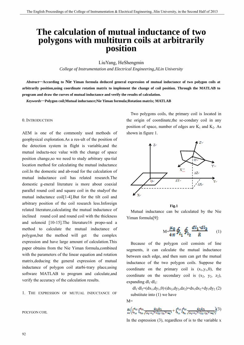
期 The English Proceedings of the College of Instrumentation & Electrical Engineering, Jilin University, in the Second Half of 2013
92
The calculation of mutual inductance of two polygons with multiturn coils at arbitrarily
position
LiuYang, HeShengmin College of Instrumentation and Electrical Engineering,JiLin University
Abstract—According to Nie Yiman formula deduced general expression of mutual inductance of two polygon coils at
arbitrarily position,using coordinate rotation matrix to implement the change of coil position. Through the MATLAB to
program and draw the curves of mutual inductance and verify the results of calculation.
Keywords—Polygon coil;Mutual inductance;Nie Yiman formula;Rotation matrix; MATLAB
0. INTRODUCTION
AEM is one of the commonly used methods of geophysical exploration.As a res-ult of the position of the detection system in flight is variable,and the mutual inducta-nce value with the change of space position change,so we need to study arbitrary spa-tial location method for calculating the mutual inductance coil.In the domestic and ab-road for the calculation of mutual inductance coil has related research.The domestic g-eneral literature is more about coaxial parallel round coil and square coil in the studyof the mutual inductance coil[1-4].But for the tilt coil and arbitrary position of the coil research less.Inforeign related literature,calculating the mutual inductance of inclined round coil and round coil with the thickness and solenoid [10-15].The literature16 propo-sed a method to calculate the mutual inductance of polygon,but the method will get the complex expression and have large amount of calculation.This paper obtains from the Nie Yiman formula,combined with the parameters of the linear equation and rotation matrix,deducing the general expression of mutual inductance of polygon coil atarbi-trary place,using software MATLAB to program and calculate,and verify the accuracy of the calculation results.
1. THE EXPRESSION OF MUTUAL INDUCTANCE OF
POLYGON COIL
Two polygons coils, the primary coil is located in the origin of coordinate,the se-condary coil in any position of space, number of edges are K1 and K2. As shown in figure 1.
Fig.1 Mutual inductance can be calculated by the Nie
Yiman formula[9]:
M= (1)
Because of the polygon coil consists of line segments, it can calculate the mutual inductance between each edge, and then sum can get the mutual inductance of the two polygon coils. Suppose the coordinate on the primary coil is (x1,y1,0), the coordinate on the secondary coil is (x2, y2, z2), expanding dl1·dl2:
dl1·dl2=(dx1,dy1,0)·(dx2,dy2,dz2)=dx1dx2+dy1dy2 (2) substitute into (1) we have
M=
(3)
In the espression (3), regardless of is to the variable x
LiuYang etc.: The calculation of mutual inductance of two polygons with multiturn coils at arbitrarily position
93
to the y integral, can involve to other variables, makes the integral the computation to be complex. Therefore, needing to eliminate other variables, transforms for includes two variable integrals.
Regarding the spatial straight line, supposes M0(a0,b0,c0) in the straight line, M(x, y, z) is in the
straight line random point,
Sv
= (m, n, p) for the
straight line direction vector,then vector with
Sv
parallel, therefore the straight line parametric
equation may write as
(4)
In the espression (4), t is a parameter.Further writes as
(5)
Use the straight line parametric equation random to express two coil sides on.Supposes a coil side two vertices is (ak,bk,ck) and (ak+1,bk+1,ck+1). May result in
m=ak+1-ak,n= ak+1-ak,p=ck+1-ck,substitutes into (5)
(6)
From this may determine parameter the range of t is [0,1].Substitutes into (3) Mij=
(7)
Using espression (7) can changes into the integral only has two variables, the integrating range is [0,1].Summing the mutual inductance of each side,we can obtain the final mutual inductance. For the multiturn coil, the turns of two coils respectively are N1 and N2, they have certain thickness, using espression (7) to calculate the mutual inductance between the single coil then sum them.
2. THE MUTUAL INDUCTANCE OF POLYGON COIL AT
ARBITRARY POSITION
Regarding the arbitrary position polygon coil in the space, we can use the three dimensional coordinates revolving matrix to carry on the coordinate transformation.Suppose the source coordinate system is O-XSYSZS, the goal coordinate system is O-XTYTZT, two coordinate system zero point translation vector is (Δx, Δy, Δz) T, any add on the zero point translation vector in the source coordinate system coordinates namely to obtain this spot in goal coordinate system coordinates [8].Spatial bitrary point A in the source coordinate system coordinates is (xs,ys,zs), in the goal coordinate system is (xT,yT,zT), then has
=R + (8)
In the formula R is the revolving matrix: R=
(9)
α、β、γ respectively is the x, y, z axis rotate Angle. Counterclockwise rotation for direction. Application coordinates revolving may realize in the random position polygon coil the coordinates transformation, substitutes into (7) then to calculate the random position the mutual inductance. Above computation process is complex, may use the MATLAB software to program and calculate.
3. THE RESULTS OF CALCULATION
(1) In order to test the correctness of the computing method,we calculate the mutual inductance of two square coaxial parallel coils with the same size. The side length of two square coils are 2a×2a, the center of coil at the origin of coordinates,the mutual inductance is expressed by M =
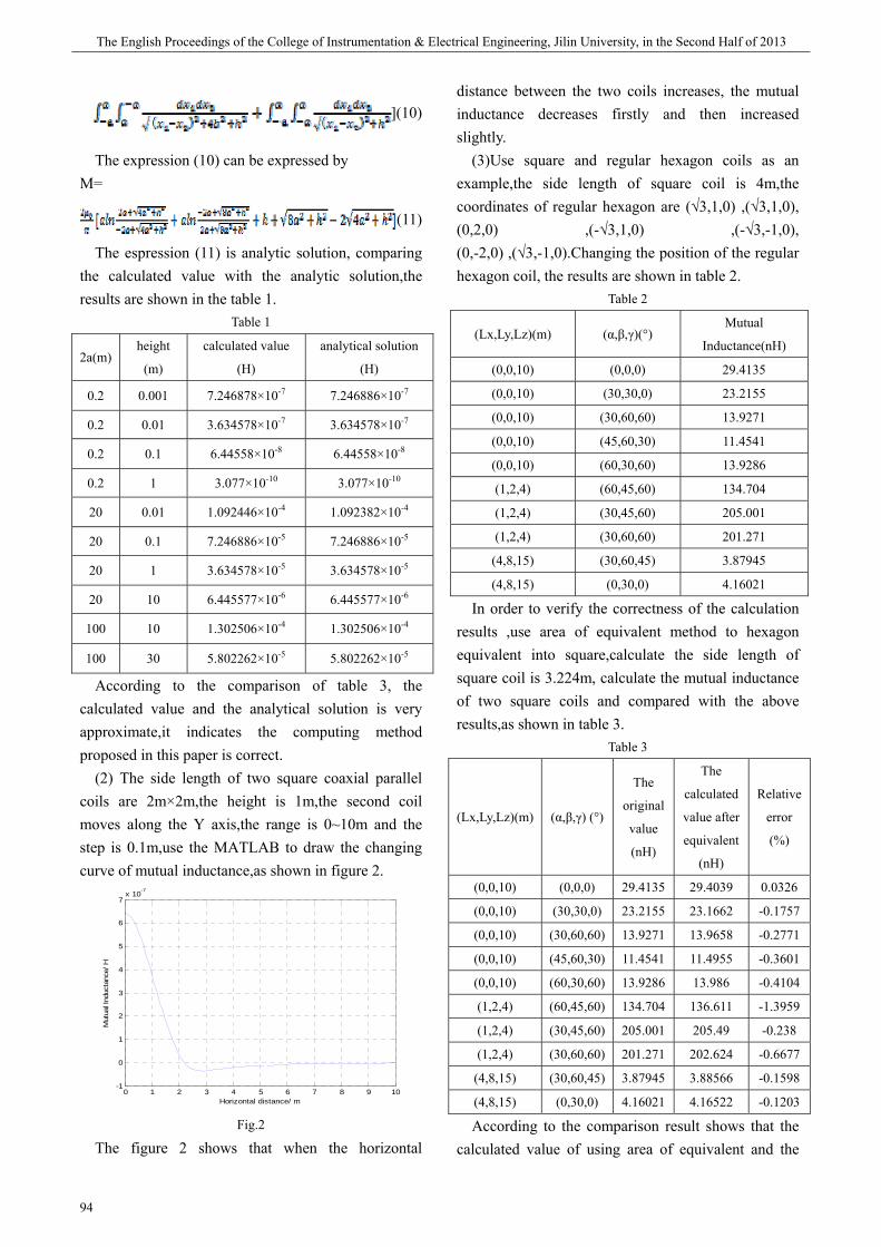
期 The English Proceedings of the College of Instrumentation & Electrical Engineering, Jilin University, in the Second Half of 2013
94
](10)
The expression (10) can be expressed by M=
(11)
The espression (11) is analytic solution, comparing the calculated value with the analytic solution,the results are shown in the table 1.
Table 1
2a(m) height
(m)
calculated value
(H)
analytical solution
(H)
0.2 0.001 7.246878×10⁻⁷ 7.246886×10⁻⁷
0.2 0.01 3.634578×10⁻⁷ 3.634578×10⁻⁷
0.2 0.1 6.44558×10⁻⁸ 6.44558×10⁻⁸
0.2 1 3.077×10⁻¹⁰ 3.077×10⁻¹⁰
20 0.01 1.092446×10⁻⁴ 1.092382×10⁻⁴
20 0.1 7.246886×10⁻⁵ 7.246886×10⁻⁵
20 1 3.634578×10⁻⁵ 3.634578×10⁻⁵
20 10 6.445577×10⁻⁶ 6.445577×10⁻⁶
100 10 1.302506×10⁻⁴ 1.302506×10⁻⁴
100 30 5.802262×10⁻⁵ 5.802262×10⁻⁵
According to the comparison of table 3, the calculated value and the analytical solution is very approximate,it indicates the computing method proposed in this paper is correct.
(2) The side length of two square coaxial parallel coils are 2m×2m,the height is 1m,the second coil moves along the Y axis,the range is 0~10m and the step is 0.1m,use the MATLAB to draw the changing curve of mutual inductance,as shown in figure 2.
0 1 2 3 4 5 6 7 8 9 10-1
0
1
2
3
4
5
6
7x 10⁻⁷
Horizontal distance/ m
Mut
ual I
nduc
tanc
e/ H
Fig.2
The figure 2 shows that when the horizontal
distance between the two coils increases, the mutual inductance decreases firstly and then increased slightly.
(3)Use square and regular hexagon coils as an example,the side length of square coil is 4m,the coordinates of regular hexagon are (√3,1,0) ,(√3,1,0), (0,2,0) ,(-√3,1,0) ,(-√3,-1,0), (0,-2,0) ,(√3,-1,0).Changing the position of the regular hexagon coil, the results are shown in table 2.
Table 2
(Lx,Ly,Lz)(m) (α,β,γ)(°) Mutual
Inductance(nH)
(0,0,10) (0,0,0) 29.4135
(0,0,10) (30,30,0) 23.2155
(0,0,10) (30,60,60) 13.9271
(0,0,10) (45,60,30) 11.4541
(0,0,10) (60,30,60) 13.9286
(1,2,4) (60,45,60) 134.704
(1,2,4) (30,45,60) 205.001
(1,2,4) (30,60,60) 201.271
(4,8,15) (30,60,45) 3.87945
(4,8,15) (0,30,0) 4.16021
In order to verify the correctness of the calculation results ,use area of equivalent method to hexagon equivalent into square,calculate the side length of square coil is 3.224m, calculate the mutual inductance of two square coils and compared with the above results,as shown in table 3.
Table 3
(Lx,Ly,Lz)(m) (α,β,γ) (°)
The
original
value
(nH)
The
calculated
value after
equivalent
(nH)
Relative
error
(%)
(0,0,10) (0,0,0) 29.4135 29.4039 0.0326
(0,0,10) (30,30,0) 23.2155 23.1662 -0.1757
(0,0,10) (30,60,60) 13.9271 13.9658 -0.2771
(0,0,10) (45,60,30) 11.4541 11.4955 -0.3601
(0,0,10) (60,30,60) 13.9286 13.986 -0.4104
(1,2,4) (60,45,60) 134.704 136.611 -1.3959
(1,2,4) (30,45,60) 205.001 205.49 -0.238
(1,2,4) (30,60,60) 201.271 202.624 -0.6677
(4,8,15) (30,60,45) 3.87945 3.88566 -0.1598
(4,8,15) (0,30,0) 4.16021 4.16522 -0.1203
According to the comparison result shows that the calculated value of using area of equivalent and the
LiuYang etc.: The calculation of mutual inductance of two polygons with multiturn coils at arbitrarily position
95
calculated results of using the method in this paper is approximate, the error is little, it indicates the calculation method in this paper is correct.
4. CONCLUSION
This paper embarks from the Nie Yiman formula, the union space straight line parametric equation and the revolving matrix infer the computation polygon coil mutual inductance the expression, this method easy to understand, so long as gives the coil various apexes the coordinates, the location parameter and the degrees rotation then calculates, and has carried on the analysis to the computed result. Using MATLAB software to program to calculate, solving the complex computation process, when the size of the coil and position are changed, only need to change the related parameters in the program, it provides a convenient way for the calculation of mutual inductance.
Referrences
[1] CenMinrui.The mutual inductance of two same
coaxial square coils[J]. Journal of WuHan
University of Engineering,2007,29(4):90-91.
[2] LiJunfeng,LiWenjie. The precise calculation of
self-induction of airborne electromagnetic
transmitter coil [J]. Geophysical computing
technology, 2007,29:17-20.
[3] ZhangXinghui et al. The mutual inductance and
the distribution of magnetic induction line of two
coaxial circular coils[J]. University physics,
2007,26(7):21-24.
[4] ZuoXiaowang et al. The discussion of mutual
inductance of two parallel coaxial circular
coils[J].Journal of HuaiYin Normal college
(Natural Science), 2010,9(5):414-416.
[5] WangShuping et al. The interactional force
between the coaxial current-carrying rectangular
coils[J]. Physics and Engineering, 2007, 17(5):
11-13.
[6] ZhuSihua and YangWanmin.The electromagnetic
force between two coaxial parallel circle
current[J]. University physics, 2005,24(10):24-26.
[7] XiangYumin.The calculation of magnetic force
between the parallel coaxial current-carrying
circular coil[J]. Journal of ChongQing
University(Natural Science), 1997,20(6):49-52.
[8] DongHongxia et al. Nonlinear coordinate
transformation model and solving methods[J].
Geomatics Technology and Equipment, 2012,14
(2):7-9.
[9] FengCizhang and MaXikui. Introduction to
Eengineering Electromagnetic Fields[M].BeiJing:
Higher Education Press,2000.
[10] Ki-Bong Kim et al. Mutual Inductance of
Noncoaxial Circular Coils with Constant Current
Density [J]. IEEE TRANSACTIONS ON
MAGNETICS,1997,33(5):4303-4309.
[11] Theodoros Theodoulidis and Robert J. Ditchburn.
Mutual Impedance of Cylindrical Coils at an
Arbitrary Positionand Orientation Above a Planar
Conductor[J]. IEEE TRANSACTIONS ON
MAGNETICS,2007,43(8):3368-3370.
[12] Slobodan I. Babic and Cevdet Akyel. Calculating
Mutual Inductance Between Circular Coils With
Inclined Axes in Air[J]. IEEE TRANSACTIONS
ON MAGNETICS,2008,44(7):1743-1750.
[13] Slobodan I. Babic and Cevdet Akyel. New
Analytic-Numerical Solutions for the Mutual
Inductance of Two Coaxial Circular Coils With
Rectangular Cross Section in Air[J]. IEEE
TRANSACTIONS ON MAGNETICS, 2006,42
(6):1661-1669.
[14] Slobodan Babic et al. Salon. New Procedures for
Calculating the Mutual Inductance of the System:
Filamentary Circular Coil-Massive Circular
Solenoid[J]. IEEE TRANSACTIONS ON
MAGNETICS,2003,39(3):1131-1134.

期 The English Proceedings of the College of Instrumentation & Electrical Engineering, Jilin University, in the Second Half of 2013
96
[15] Slobodan Babic et al.Mutual Inductance
Calculation Between Circular Filaments
Arbitrarily Positioned in Space: Alternative to
Grover’s Formula[J]. IEEE TRANSACTIONS
ON MAGNETICS,2010,46(9):3591-3600.
[16] L.Hannakam and E.Nolle,Berlin.Programm zur
Bestimmung der Gegeninduktivität räumlicher
polygonartiger Leiterschleifen.Archiv für
Elektrotechnik,1981.
Han Si-yu etc.: Design and Realization of a Secondary Reclosing Microcomputer Device Remotely and Interactively Controlled by PC
97
Design and Realization of a Secondary Reclosing Microcomputer Device Remotely and Interactively
Controlled by PC
Han Si-yu, Wang Yu, Ma Jing (College of instrumentation & Electrical Engineering, Jilin University, Changchun 130001, China)
Abstract—Traditional reclosing device have complex wiring and much auxiliary equipments. It cannot achieve contact-free
setting and control of staff, and it often malfunctions and refuses to work. If the fault does not eliminate in a short time,
reclosing device may trip again. It makes that the success rate is not high. This paper designed a secondary reclosing
microcomputer device remotely and interactively controlled by PC. The device is based on MSP430F149 single-chip, with low
power consumption, low cost, real-time display of data, single-chip reclosing control, remotely and interactively controlled by
PC and so on. The device mainly consists of the power supply module, the acquisition module of voltage signal, single-chip
module, relay module, display module, communication module, PC visual interface and other components. This paper
describes the hardware circuit design, and flow chart of the software procedure. We test the installation in a lab environment,
it implements the single-chip microcomputer reclosing operation for the second time and it can be displayed and controlled by
the host computer.
Keywords—single-chip; secondary reclosing device; remote interaction; the host computer
INTRODUCTION
AS demand of social development for power is increasing, the number of transmission line failures is growing. The basic reason of these failures is a long running outdoors. Transmission line is in the natural environment, and it is influenced by climate, flora and fauna, human activities such as porcelain insulator surface flashover caused by lightning, the touch line caused by strong winds, the line short circuit through the birds and the branches. Such failures are called transient faults which take up 90% of the entire line faults. When the fault disappeared later, if carried out by the operator manually coincide, due to power outages for a long time, most user motors have stalled and the effect of closing is not significant. As a result currently on the market people use the automatic reclosing device. Automatic reclosing (ARC) is an automatic device which automatically inputs circuit as required when the circuit breaker jumps due to failure. Traditional reclosing device uses analog circuitry for a closing operation. On one hand, connection of device is complex, there are many auxiliary equipments and high rate of wrong operation, on the other hand the device could not return to the slower switching in the
fault point and could not remotely monitor and control for real time. Therefore, how to design a reclosing equipment which is simple, effective and has high successful rate.
Currently the secondary reclosing microcomputer device remotely and interactively controlled by PC is still in the early research. Microcomputer-based reclosing device has high reliability, high precision, high speed and intelligent communication, quick and convenience, simple structure, and other advantages. We just has a certain control settings, they can pose a variety of ways. When the auto-reclosing coincides on a permanent failure many times, the system is suffered several attacks, and it results in serious consequences. So safety and success rate shows that reclosing II is the most appropriate. In recent years a reclosing device had been widely applied in Guangzhou area. It is a technology which makes use of composition of feeder circuit breaker device in power distribution system and on-post switch in action to make sure fault location and isolation and rapidly restore power supply. But it failed to realize the remote display and control.
In order to achieve a simple, effective and high successful rate of reclosing device.This paper designs a secondary reclosing microcomputer device remotely and interactively controlled by PC. The device selects
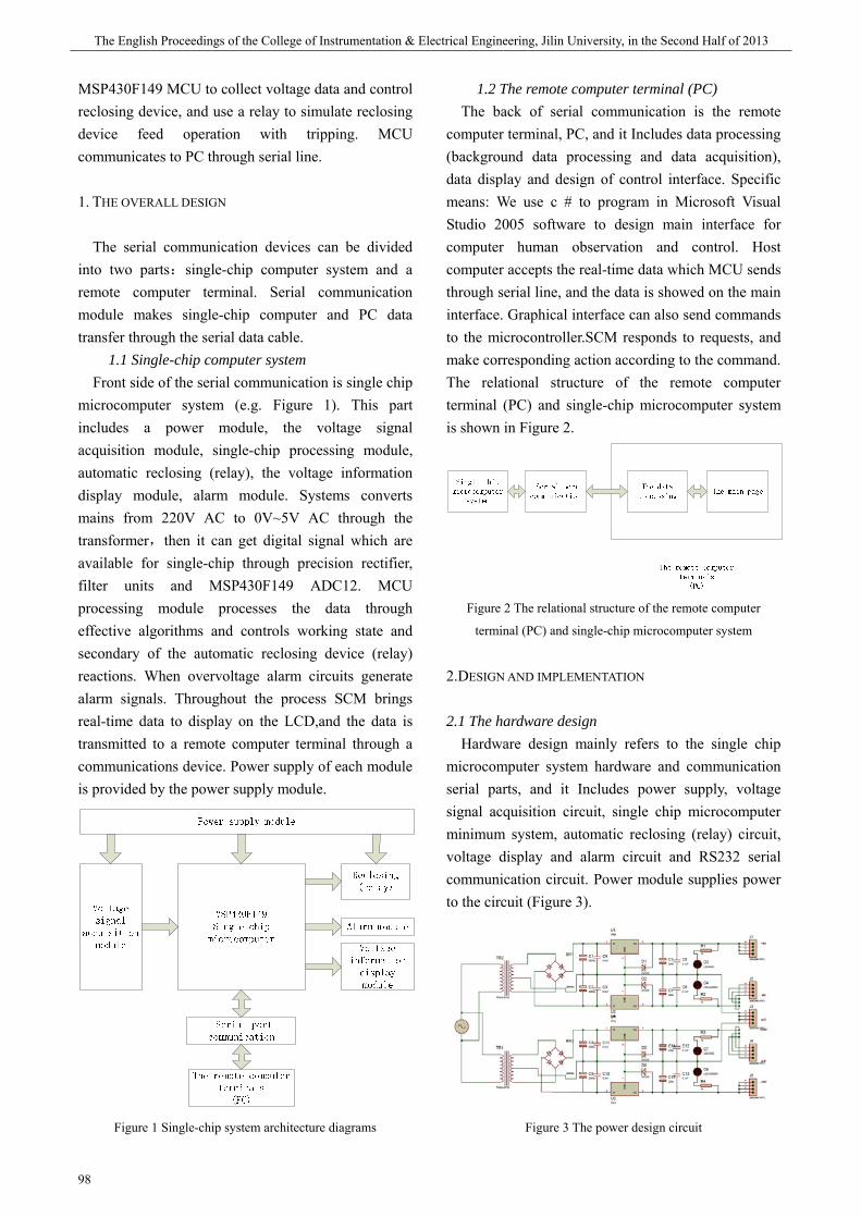
期 The English Proceedings of the College of Instrumentation & Electrical Engineering, Jilin University, in the Second Half of 2013
98
MSP430F149 MCU to collect voltage data and control reclosing device, and use a relay to simulate reclosing device feed operation with tripping. MCU communicates to PC through serial line.
1. THE OVERALL DESIGN
The serial communication devices can be divided into two parts:single-chip computer system and a remote computer terminal. Serial communication module makes single-chip computer and PC data transfer through the serial data cable.
1.1 Single-chip computer system Front side of the serial communication is single chip
microcomputer system (e.g. Figure 1). This part includes a power module, the voltage signal acquisition module, single-chip processing module, automatic reclosing (relay), the voltage information display module, alarm module. Systems converts mains from 220V AC to 0V~5V AC through the transformer,then it can get digital signal which are available for single-chip through precision rectifier, filter units and MSP430F149 ADC12. MCU processing module processes the data through effective algorithms and controls working state and secondary of the automatic reclosing device (relay) reactions. When overvoltage alarm circuits generate alarm signals. Throughout the process SCM brings real-time data to display on the LCD,and the data is transmitted to a remote computer terminal through a communications device. Power supply of each module is provided by the power supply module.
Figure 1 Single-chip system architecture diagrams
1.2 The remote computer terminal (PC) The back of serial communication is the remote
computer terminal, PC, and it Includes data processing (background data processing and data acquisition), data display and design of control interface. Specific means: We use c # to program in Microsoft Visual Studio 2005 software to design main interface for computer human observation and control. Host computer accepts the real-time data which MCU sends through serial line, and the data is showed on the main interface. Graphical interface can also send commands to the microcontroller.SCM responds to requests, and make corresponding action according to the command. The relational structure of the remote computer terminal (PC) and single-chip microcomputer system is shown in Figure 2.
Figure 2 The relational structure of the remote computer
terminal (PC) and single-chip microcomputer system
2.DESIGN AND IMPLEMENTATION
2.1 The hardware design Hardware design mainly refers to the single chip
microcomputer system hardware and communication serial parts, and it Includes power supply, voltage signal acquisition circuit, single chip microcomputer minimum system, automatic reclosing (relay) circuit, voltage display and alarm circuit and RS232 serial communication circuit. Power module supplies power to the circuit (Figure 3).
Figure 3 The power design circuit

Han Si-yu etc.: Design and Realization of a Secondary Reclosing Microcomputer Device Remotely and Interactively Controlled by PC
99
2.1.1 Voltage signal acquisition circuit Voltage signal acquisition circuit plays an important
role in the entire unit. Amplification of the circuit, anti-interference ability and stability directly affect the accuracy of the data collected.
Voltage acquisition circuit part mainly includes the voltage regulation, rectifier circuit, filter circuit parts. Voltage transformer's primary function makes the mains (220V) voltages through transformers transform around 5V AC. The voltage regulation part adjusts the size of the ac voltage. Then the voltage signals go into voltage regulator parts and rectifiers through a rectifier and export stable DC signal. The voltage signal is filtered through the filter circuit. It filters the signal waveform of high frequency components and gets smaller dc ripple waveform. By changing the voltage regulation part slide rheostat, we make the output dc voltage value between 0 V to 3.3 V to meet the requirement of ADC12 built-in the microprocessor MSP430 to input voltage amplitude of analog signal.
a) Voltage regulating part AC voltage of input first step-down the voltage
regulator control, and we can manually adjust the sliding rheostat to change the input voltage. Figure 4 is the voltage circuit of voltage transformer.
Figure 4 voltage circuit of voltage transformer
b) Rectifier circuit part
Figure 5 rectifier circuit
Figure 5 is the rectifier circuit. Input voltage is .
Output voltage is . R3 is and R4 is . is
output voltage of first UA741. Related formula such as (1) to (4):
When
(1)
When
(2)
(3)
When
(4)
c) Filter circuit part
Figure 6 Filter circuit diagram
Figure 6 is filter circuit diagram. Second-order active filter circuit is composed of two sections composed with RC filter circuit and amplifier. Its characteristic is high input impedance, low output impedance. Proportion amplifier voltage gain is pass band voltage gain of low pass filter
= =1+( -1) /
The basic formula of the filter circuit, such as (5) to (7) :
= (5)
Q= (6)
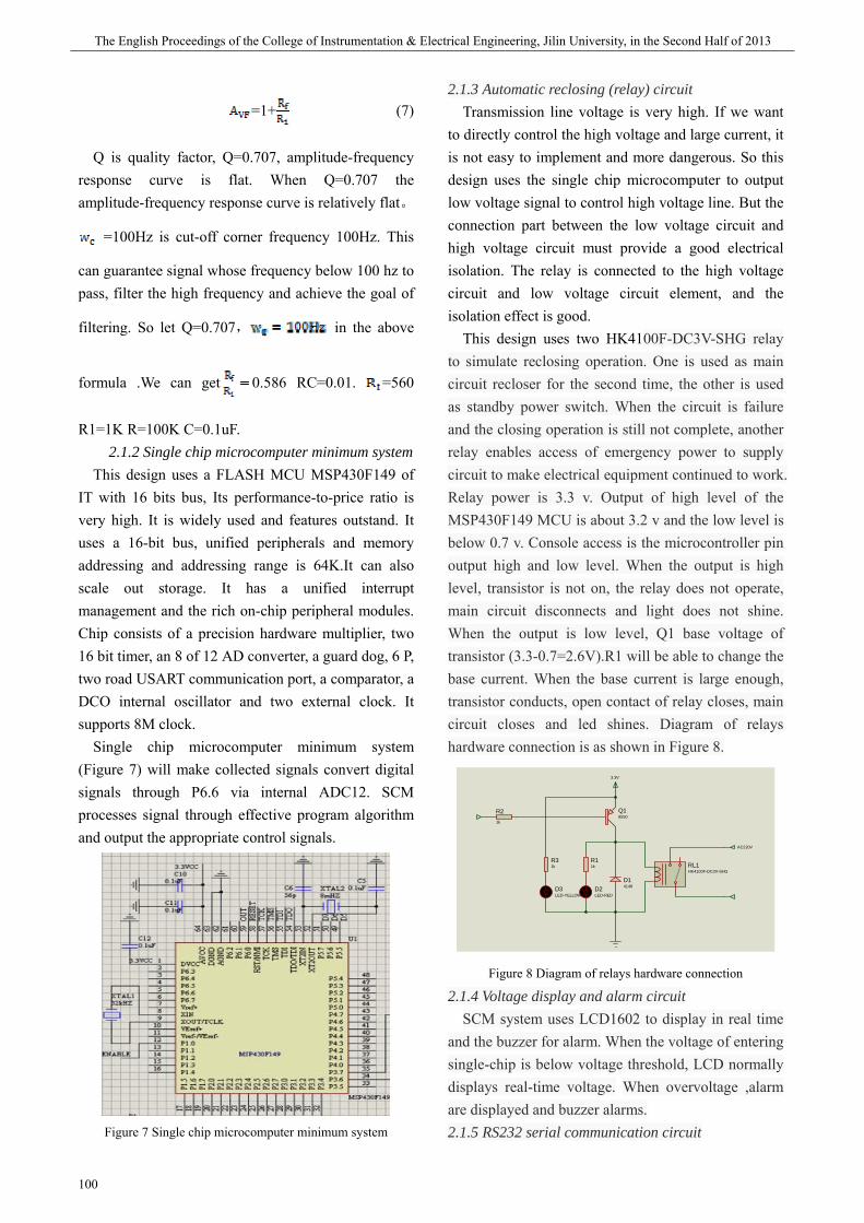
期 The English Proceedings of the College of Instrumentation & Electrical Engineering, Jilin University, in the Second Half of 2013
100
=1+ (7)
Q is quality factor, Q=0.707, amplitude-frequency response curve is flat. When Q=0.707 the amplitude-frequency response curve is relatively flat。
=100Hz is cut-off corner frequency 100Hz. This
can guarantee signal whose frequency below 100 hz to pass, filter the high frequency and achieve the goal of
filtering. So let Q=0.707, in the above
formula .We can get 0.586 RC=0.01. =560
R1=1K R=100K C=0.1uF. 2.1.2 Single chip microcomputer minimum system
This design uses a FLASH MCU MSP430F149 of IT with 16 bits bus, Its performance-to-price ratio is very high. It is widely used and features outstand. It uses a 16-bit bus, unified peripherals and memory addressing and addressing range is 64K.It can also scale out storage. It has a unified interrupt management and the rich on-chip peripheral modules. Chip consists of a precision hardware multiplier, two 16 bit timer, an 8 of 12 AD converter, a guard dog, 6 P, two road USART communication port, a comparator, a DCO internal oscillator and two external clock. It supports 8M clock.
Single chip microcomputer minimum system (Figure 7) will make collected signals convert digital signals through P6.6 via internal ADC12. SCM processes signal through effective program algorithm and output the appropriate control signals.
Figure 7 Single chip microcomputer minimum system
2.1.3 Automatic reclosing (relay) circuit Transmission line voltage is very high. If we want
to directly control the high voltage and large current, it is not easy to implement and more dangerous. So this design uses the single chip microcomputer to output low voltage signal to control high voltage line. But the connection part between the low voltage circuit and high voltage circuit must provide a good electrical isolation. The relay is connected to the high voltage circuit and low voltage circuit element, and the isolation effect is good.
This design uses two HK4100F-DC3V-SHG relay to simulate reclosing operation. One is used as main circuit recloser for the second time, the other is used as standby power switch. When the circuit is failure and the closing operation is still not complete, another relay enables access of emergency power to supply circuit to make electrical equipment continued to work. Relay power is 3.3 v. Output of high level of the MSP430F149 MCU is about 3.2 v and the low level is below 0.7 v. Console access is the microcontroller pin output high and low level. When the output is high level, transistor is not on, the relay does not operate, main circuit disconnects and light does not shine. When the output is low level, Q1 base voltage of transistor (3.3-0.7=2.6V).R1 will be able to change the base current. When the base current is large enough, transistor conducts, open contact of relay closes, main circuit closes and led shines. Diagram of relays hardware connection is as shown in Figure 8.
RL1HK4100F-DC3V-SHG
AC220V
Q18550
R11k
D2LED-RED
D14148
R21k
3.3V
R31k
D3LED-YELLOW
Figure 8 Diagram of relays hardware connection
2.1.4 Voltage display and alarm circuit SCM system uses LCD1602 to display in real time
and the buzzer for alarm. When the voltage of entering single-chip is below voltage threshold, LCD normally displays real-time voltage. When overvoltage ,alarm are displayed and buzzer alarms. 2.1.5 RS232 serial communication circuit
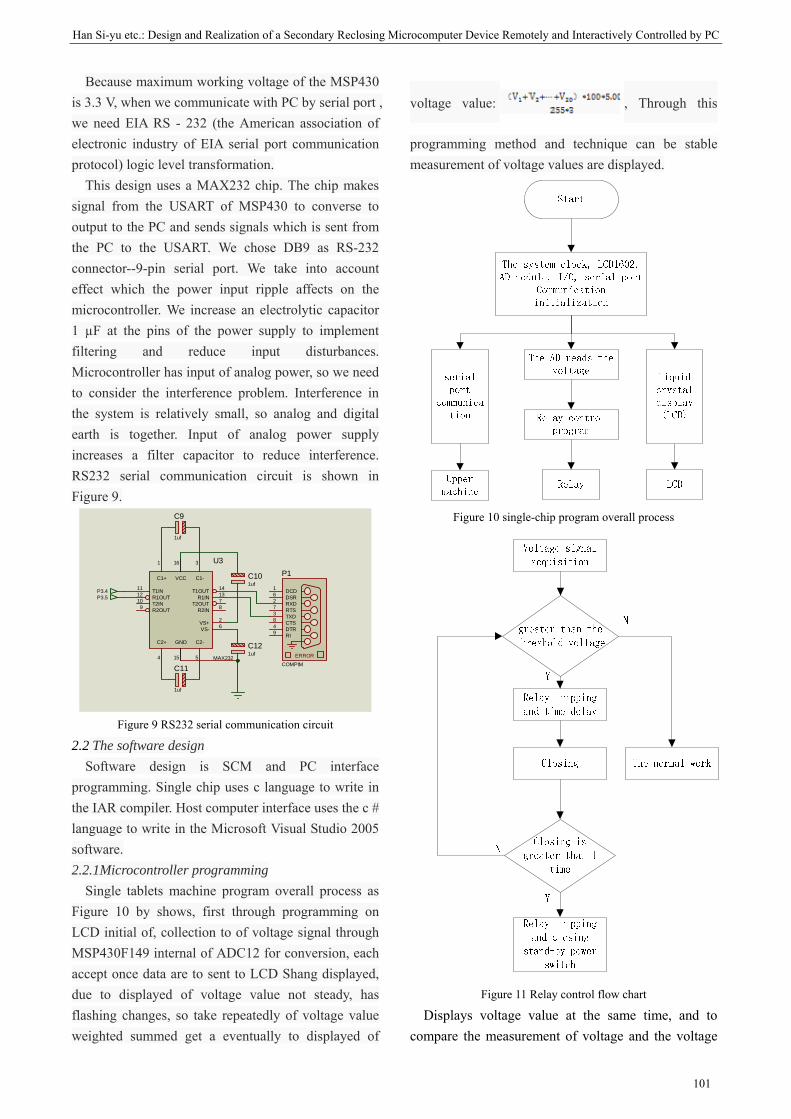
Han Si-yu etc.: Design and Realization of a Secondary Reclosing Microcomputer Device Remotely and Interactively Controlled by PC
101
Because maximum working voltage of the MSP430 is 3.3 V, when we communicate with PC by serial port , we need EIA RS - 232 (the American association of electronic industry of EIA serial port communication protocol) logic level transformation.
This design uses a MAX232 chip. The chip makes signal from the USART of MSP430 to converse to output to the PC and sends signals which is sent from the PC to the USART. We chose DB9 as RS-232 connector--9-pin serial port. We take into account effect which the power input ripple affects on the microcontroller. We increase an electrolytic capacitor 1 µF at the pins of the power supply to implement filtering and reduce input disturbances. Microcontroller has input of analog power, so we need to consider the interference problem. Interference in the system is relatively small, so analog and digital earth is together. Input of analog power supply increases a filter capacitor to reduce interference. RS232 serial communication circuit is shown in Figure 9.
T1IN11
R1OUT12
T2IN10
R2OUT9
T1OUT 14
R1IN 13
T2OUT 7
R2IN 8
C2+
4
C2-
5
C1+
1
C1-
3
VS+ 2
VS- 6
VCC
16
GND
15
U3
MAX232 ERROR
TXD3
RXD2
CTS8
RTS7
DSR6
DTR4
DCD1
RI9
P1
COMPIM
C9
1uf
C11
1uf
C121uf
P3.4P3.5
C101uf
Figure 9 RS232 serial communication circuit
2.2 The software design Software design is SCM and PC interface
programming. Single chip uses c language to write in the IAR compiler. Host computer interface uses the c # language to write in the Microsoft Visual Studio 2005 software. 2.2.1Microcontroller programming
Single tablets machine program overall process as Figure 10 by shows, first through programming on LCD initial of, collection to of voltage signal through MSP430F149 internal of ADC12 for conversion, each accept once data are to sent to LCD Shang displayed, due to displayed of voltage value not steady, has flashing changes, so take repeatedly of voltage value weighted summed get a eventually to displayed of
voltage value: , Through this
programming method and technique can be stable measurement of voltage values are displayed.
Figure 10 single-chip program overall process
Figure 11 Relay control flow chart
Displays voltage value at the same time, and to compare the measurement of voltage and the voltage
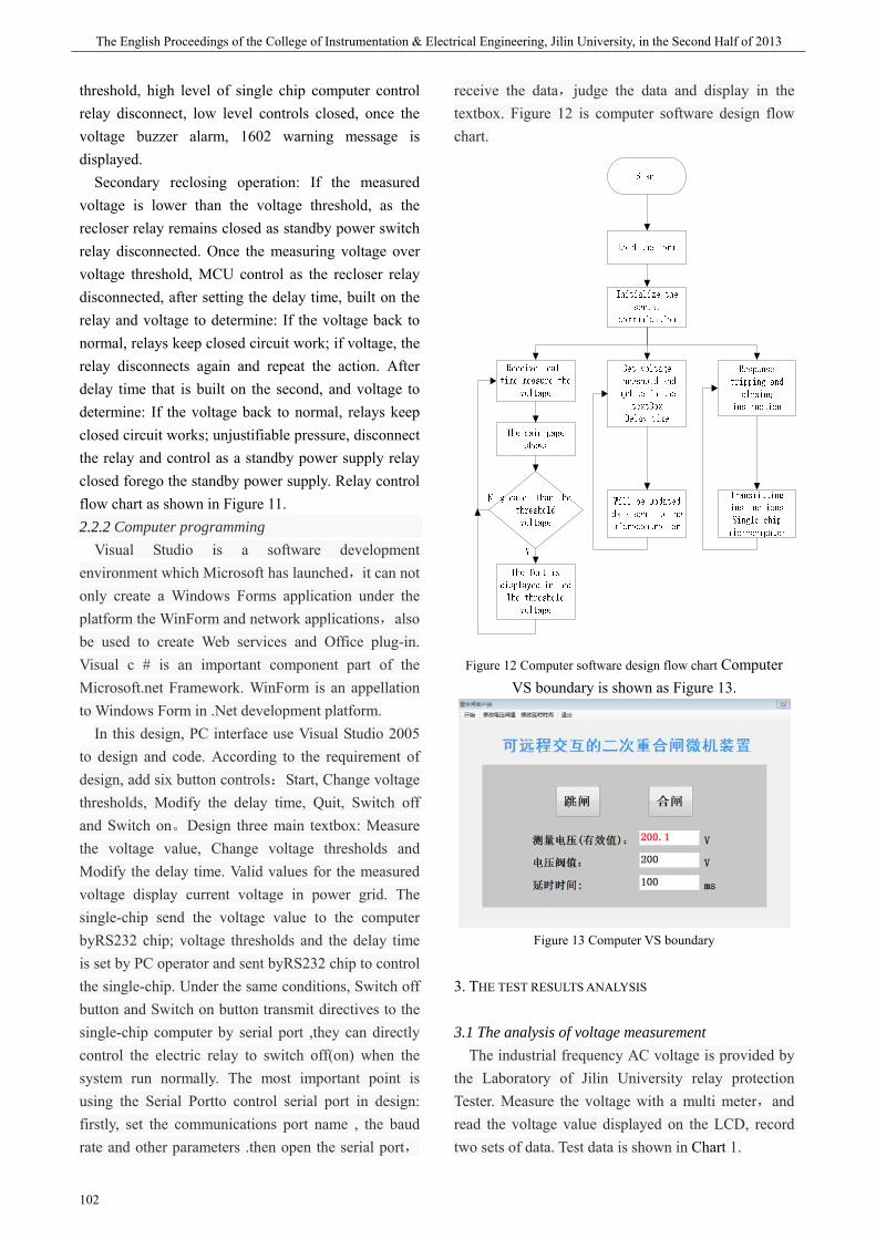
期 The English Proceedings of the College of Instrumentation & Electrical Engineering, Jilin University, in the Second Half of 2013
102
threshold, high level of single chip computer control relay disconnect, low level controls closed, once the voltage buzzer alarm, 1602 warning message is displayed.
Secondary reclosing operation: If the measured voltage is lower than the voltage threshold, as the recloser relay remains closed as standby power switch relay disconnected. Once the measuring voltage over voltage threshold, MCU control as the recloser relay disconnected, after setting the delay time, built on the relay and voltage to determine: If the voltage back to normal, relays keep closed circuit work; if voltage, the relay disconnects again and repeat the action. After delay time that is built on the second, and voltage to determine: If the voltage back to normal, relays keep closed circuit works; unjustifiable pressure, disconnect the relay and control as a standby power supply relay closed forego the standby power supply. Relay control flow chart as shown in Figure 11. 2.2.2 Computer programming
Visual Studio is a software development environment which Microsoft has launched,it can not only create a Windows Forms application under the platform the WinForm and network applications,also be used to create Web services and Office plug-in. Visual c # is an important component part of the Microsoft.net Framework. WinForm is an appellation to Windows Form in .Net development platform.
In this design, PC interface use Visual Studio 2005 to design and code. According to the requirement of design, add six button controls:Start, Change voltage thresholds, Modify the delay time, Quit, Switch off and Switch on。Design three main textbox: Measure the voltage value, Change voltage thresholds and Modify the delay time. Valid values for the measured voltage display current voltage in power grid. The single-chip send the voltage value to the computer byRS232 chip; voltage thresholds and the delay time is set by PC operator and sent byRS232 chip to control the single-chip. Under the same conditions, Switch off button and Switch on button transmit directives to the single-chip computer by serial port ,they can directly control the electric relay to switch off(on) when the system run normally. The most important point is using the Serial Portto control serial port in design: firstly, set the communications port name , the baud rate and other parameters .then open the serial port,
receive the data,judge the data and display in the textbox. Figure 12 is computer software design flow chart.
Figure 12 Computer software design flow chart Computer VS boundary is shown as Figure 13.
Figure 13 Computer VS boundary
3. THE TEST RESULTS ANALYSIS
3.1 The analysis of voltage measurement The industrial frequency AC voltage is provided by
the Laboratory of Jilin University relay protection Tester. Measure the voltage with a multi meter,and read the voltage value displayed on the LCD, record two sets of data. Test data is shown in Chart 1.

Han Si-yu etc.: Design and Realization of a Secondary Reclosing Microcomputer Device Remotely and Interactively Controlled by PC
103
Chart 1 Actual voltage and displayed voltage comparison chart
Num Actual voltage(V) Displayed voltage(V)
1 80.1 80.6
2 90.2 90.7
3 98.6 98.9
4 109.4 110.0
5 119.7 120.1
6 130.6 130.2
7 140.4 140.3
8 150.4 150.4
9 160.5 160.5
10 170.5 170.6
11 180.3 180.7
12 190.4 190.7
13 200.2 200.8
14 210.3 210.0
15 220.6 220.1
16 230.4 230.2
17 240.6 240.3
18 250.5 250.4
The curve between actual voltage and displayed voltage is shown in Figure 14.
Figure 14 The curve between actual voltage and displayed
voltage
It can be found through the chart and diagram that the curve between actual voltage and displayed voltage is closed to linear change. It proves that the device for measuring the voltage is really reliable and useful. 3.2 The single-chip control results analysis
a)Single-chip can receive and display the actual voltage values in real-time,Error less than 1V.
b)When the voltage value exceeds the voltage thresholds for the first time, LCD alarms and buzzer rings. The normally open recloser relay switch off and
Light is put out. After the delay time which is set by pc,the relay switch on for the first time. If the voltage is lower than the threshold voltage,then the system is back to normal. If the voltage is more than the threshold voltage, then repeat the above actions. Because of the single-chip’s high speed , the phenomenon people observed with the naked eye is that the light is lit once time.
c)After the second delay,the relay switch on for the second time. If the voltage is lower than the threshold voltage,then the system is back to normal. If the voltage is more than the threshold voltage,then the recloser relay switch off. As the same time, switch on the standby relay in order to let the standby power run. 3.3Analysis of PC control
One side,Pc can display the voltage value sent by single-chip. On the other side, PC can Change voltage thresholds and Modify the delay time. When the voltage is lower than the threshold voltage, Pc can control the relay by the button switch off and button switch on. These above all use the SerialPort.If the voltage is more than the threshold voltage, font color turns from black to red for alarm.
4. CONCLUSIONS
The design completes the desired goals. Measure the voltage value, control there closer relay and other external device and realize the PC remotely display and control by the SerialPort. It is efficient, convenient and practical. It has a certain market prospects. In the future work, we will use wireless or network data transmission instead of cable transmission, complete voltage signal acquisition module optimization and integration to improved PC control function.
Reference
[1] Yuan Yue, Zhang Bao. research status quo and
prospect of automatic reclosing in power
system [J]. China, (1997): 44-47.
[2] Zhang Xiangjun. traditional and modern
analysis of microcomputer-based integrated
automatic reclosing device [J]. Journal of
Liaoning Institute of science and technology,
期 The English Proceedings of the College of Instrumentation & Electrical Engineering, Jilin University, in the Second Half of 2013
104
2008 (3): 1-2.
[3] Zhou Xingkui, Tian Jianwen. New type of
microcomputer principle and application of
automatic reclosing [j]. Gansu water resources
and hydropower technology, 2011 (11): 12-15.
[4] Long Qifeng, Chen Hao. Secondary cause of
coincident failure analysis [J].
Electrotechnical, 2012 (12): 10-13.
[5] Chan Ming fai, Zhang Shaofang, Wen
Fushuan. Second enclosure and secondary
secondary recloser application in distribution
system [J]. Journal of North China electric
power University, 2011,38 (2): 21-26.
[6] Wang Zhibin, Yang Haiping. discussion on
reclosing and automatically restore power
supply [J]. Journal of Chongqing electric
power, 2005,10 (1): 1-3.
[7] Xu Hailong. Transmission line transient faults
and preliminary analysis of the effect of
automatic recloser [J]. mechanical and
electronic information (2012): 32-33.
[8] Han Xiao, Zhao Guoyu, RANDT, Li Yongjing,
Tian Zhuang. reclosure reasons analysis and
prevention measures of misoperation [J].
electric power system protection and control,
2010,38 (24): 217-221.
[9] Wang Tikui, Guo Jianqiang, Gao Xiaorong, Li
Wang. Adaptive auto-reclosure in combination
with relay protection [J]. modern electronic
technology, 2011,34 (16): 126-129.
[10] Liu Xin. saying auto-reclosing [J]. rural
electrician, 2009,5:33.
[11] HE Qiao,DUAN Qingming, QIU chun ling.
Microcontroller Microcontroller Theory and
Applications [M] Beijing: China Railway
Press,2004.3
[12] XieGuangrun. Power system over-voltage [M].
Beijing: Water Power Press,1985
[13] GaoLiang. Microcomputer relay protection of
power system [M].Beijing: China Electric Power
Press,2007
[14] ian Ji, Cao Junbiao, Wang Fulin. Protection
experiments Device [J]. Jilin electrification
College Department of Automatic Control.
[15] Guo Panfeng. Design and research of wireless
ECG data transmission based on Zigbee
protocol[J].Anhui University.
[16] Wei Mingbao,Li Xiaomei. New computer
protection device hardware and software[J].
Shandong University of Science and Technology
[17] Tan Haoqiang. C programming (third edition) [M].
Beijing: Tsinghua University Press, 2005.7
[18] Wang Haixia. Design of single-chip
microcomputer and PC serial communication [J].
the school of Weifang

Wang Di etc.: The Design and Implementation of Electromagnetic Radiation Detector
105
The Design and Implementation of Electromagnetic Radiation Detector
Wang Di, Ren Tian-ming, Jiang Ming-jie
College of Instrumentation & Electrical Engineering, Jilin University, Changchun, Jilin Province 130001 Abstract—This paper describes an approach of electromagnetic radiation detector based on MSP430F149, the
instrument uses a conventional antenna for the sensor by the filter, amplifier, AD modules and nRF905 wireless
module and the 12864 LCD module. Various points transmit the measured data through the wireless module, the
final summary via LCD display interface implementation. Available on the market capable of electromagnetic
radiation detector operating under artificial point is detected to detect electromagnetic radiation, but the detection
must be manually turned on, because of the human factors, it can’t achieve the real-time detection point is
detected. Meanwhile, in the detection point is large, the current detector can be sequentially detected, the
summary of a plurality of data can’t be displayed. This mode of operation will waste manpower to a certain extent,
reduce the efficiency of detection of electromagnetic radiation. This paper presents a multi-point simultaneous
measurement and display of the measured data aggregation electromagnetic radiation detector design ideas and
methods. This paper details the hardware circuit design of the instrument composition, and related software
module debugging results, and the final experimental results show.
Keywords—microcontroller; electromagnetic radiation; wireless transmission; real-time display
0 INTRODUCTIONS
WITH the development of modern electronic technology, people's work and life requires frequent use of a variety of electronic devices. The operation of electronic equipment will inevitably produce different levels of electromagnetic radiation (electric and magnetic fields generated by the interaction of electromagnetic waves change, electromagnetic waves emitted into the air or disclosure of the phenomenon, called electromagnetic radiation), thus most of the time people are exposed to electromagnetic radiation. Electromagnetic radiation can be described as "invisible killer", studies show that electromagnetic radiation on human health has a great impact, although it is keen to reduce the harm of electromagnetic radiation, but the face of the damage can’t be captured with the naked eye what should do?
Presently existing electromagnetic radiation detection apparatus has been able to be detected value of the point measurement of electromagnetic radiation, but sometimes it is necessary to point electromagnetic radiation for.
Long-term detection, or both a plurality of detection
points are detected, for example, by detecting electrical equipment electromagnetic radiation value to determine whether the device is running, check the line if there is leakage risks. This requires testing equipment can work stable without human control for a long time and a plurality of detectors can be integrated with data locations to be monitored. However, the existing equipment can’t be achieved with timeliness and the ability to integrate testing.
In order to make electromagnetic detection technology more suit life and industrial production, to achieve real-time detection of electromagnetic radiation and data integration. The design of this electromagnetic radiation detector based on traditional detection devices, increased wireless data transmission part, through the nRF905 wireless transmission module data of the various monitoring points are sent to the host computer, and then through the LCD display module.
1 THE OVERALL DESIGN
The instrument can be divided into the signal acquisition and processing and sending part (the machine) and the signal receiving and integrated

期 The English Proceedings of the College of Instrumentation & Electrical Engineering, Jilin University, in the Second Half of 2013
106
display part (PC). The machine receives electromagnetic signal through the antenna as the sensor in the space, the signal will travel through the filter circuit interference signal filtering, and the processed signal is amplified by amplifying circuit. Through the AD conversion module we convert electrical signals into digital signals, finally through the wireless transmitting to PC. PC will receive the signal with a wireless first, and then through the LCD it will be displayed. In general the PC part is the key of the whole instrument design.
(a)upper conputer (b)Lower machine
Figure 1 The overall design diagram
2 THE DESIGN OF HARDWARE CIRCUIT
2.1 The Upper Machine Design 2.1.1 Sensor
The sensor part adopts antenna for receiving electromagnetic signal as the equipment. Electromagnetic radiation in the space can be divided into electric field radiation components and magnetic radiation. Induced electric field, electric field radiation is made and voltage unit is the V/m. Magnetic field radiation is due to A current, the magnetic induction unit is the A/m. So the unit of electromagnetic radiation is including W/m2, namely the power density. Antenna as a sensor device has wide frequency band, it can accurate induced electric field, magnetic field, detection of space power distribution and so on, it just meet the design requirements of the instrument.
2.1.2 The filter and amplifying circuit The signal collected by the antenna sensor need to
filter out the high frequency component, keeping low frequency components, so the filter circuit is designed for active low-pass filter circuit. Because signals the antenna acquisition are faint, so after filtering to enlarge it, to meet the requirements of the follow-up circuit of voltage. This design adopts the basic (including A741 as the main chip amplifier circuit. Including A741 is simple to operate, simple circuit structure and other advantages. The design for the + 12 v working voltage and power supply voltage of power supply. We need to extern resistance through 2 pin and 3 pin to adjust its magnification.
Figure 2 μA741 Pin diagram
Figure 3 μA741 The circuit connection diagram
4
1
1
14
R
U
R
UU=
− ①
3
32
2
25
R
UU
R
UU −=
− ②
if1
4
2
3
R
R
R
R= ; then
)( 54
2
33 UU
R
RU −=
We can change the magnification and the resistance and the change of output voltage with
changing 2R and 3R .
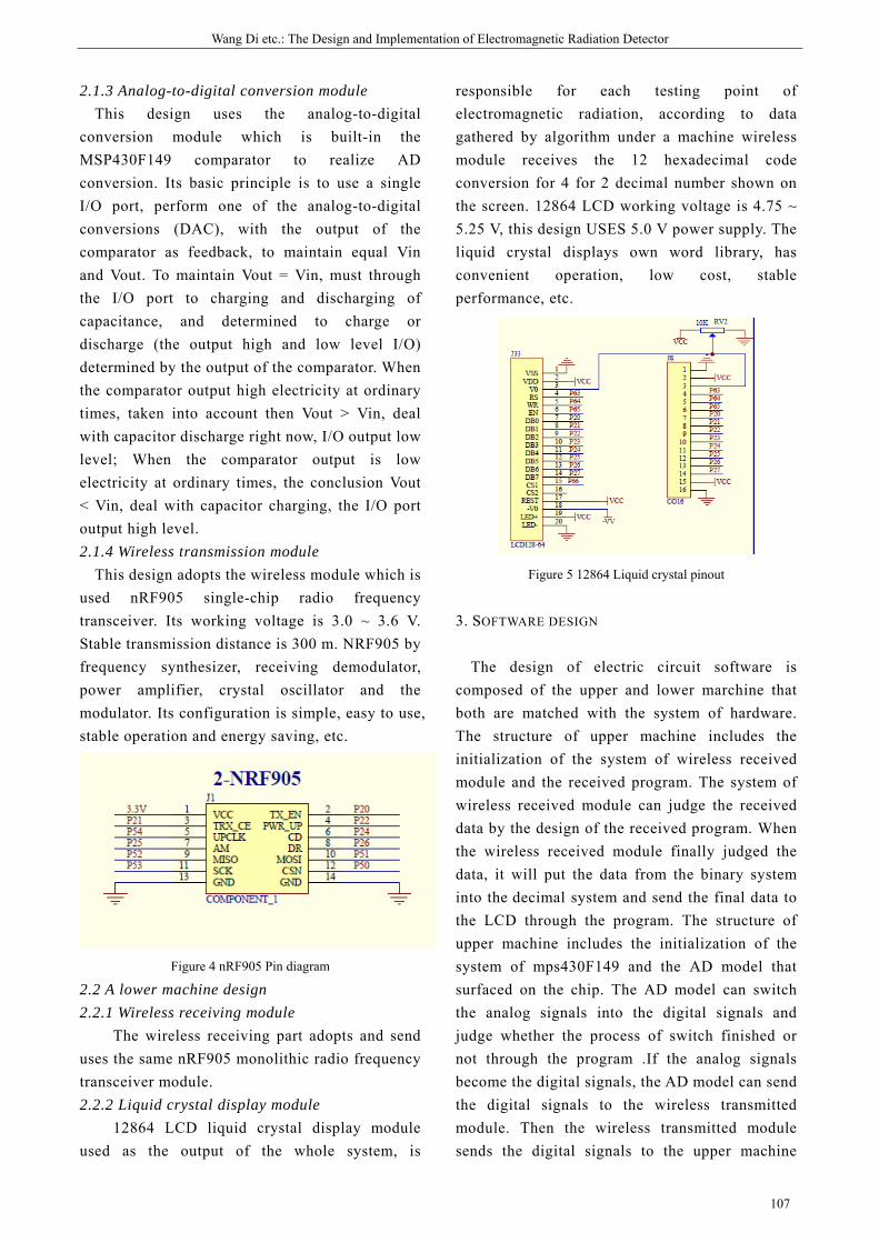
Wang Di etc.: The Design and Implementation of Electromagnetic Radiation Detector
107
2.1.3 Analog-to-digital conversion module This design uses the analog-to-digital
conversion module which is built-in the MSP430F149 comparator to realize AD conversion. Its basic principle is to use a single I/O port, perform one of the analog-to-digital conversions (DAC), with the output of the comparator as feedback, to maintain equal Vin and Vout. To maintain Vout = Vin, must through the I/O port to charging and discharging of capacitance, and determined to charge or discharge (the output high and low level I/O) determined by the output of the comparator. When the comparator output high electricity at ordinary times, taken into account then Vout > Vin, deal with capacitor discharge right now, I/O output low level; When the comparator output is low electricity at ordinary times, the conclusion Vout < Vin, deal with capacitor charging, the I/O port output high level. 2.1.4 Wireless transmission module
This design adopts the wireless module which is used nRF905 single-chip radio frequency transceiver. Its working voltage is 3.0 ~ 3.6 V. Stable transmission distance is 300 m. NRF905 by frequency synthesizer, receiving demodulator, power amplifier, crystal oscillator and the modulator. Its configuration is simple, easy to use, stable operation and energy saving, etc.
Figure 4 nRF905 Pin diagram
2.2 A lower machine design 2.2.1 Wireless receiving module
The wireless receiving part adopts and send uses the same nRF905 monolithic radio frequency transceiver module. 2.2.2 Liquid crystal display module
12864 LCD liquid crystal display module used as the output of the whole system, is
responsible for each testing point of electromagnetic radiation, according to data gathered by algorithm under a machine wireless module receives the 12 hexadecimal code conversion for 4 for 2 decimal number shown on the screen. 12864 LCD working voltage is 4.75 ~ 5.25 V, this design USES 5.0 V power supply. The liquid crystal displays own word library, has convenient operation, low cost, stable performance, etc.
Figure 5 12864 Liquid crystal pinout
3. SOFTWARE DESIGN
The design of electric circuit software is composed of the upper and lower marchine that both are matched with the system of hardware. The structure of upper machine includes the initialization of the system of wireless received module and the received program. The system of wireless received module can judge the received data by the design of the received program. When the wireless received module finally judged the data, it will put the data from the binary system into the decimal system and send the final data to the LCD through the program. The structure of upper machine includes the initialization of the system of mps430F149 and the AD model that surfaced on the chip. The AD model can switch the analog signals into the digital signals and judge whether the process of switch finished or not through the program .If the analog signals become the digital signals, the AD model can send the digital signals to the wireless transmitted module. Then the wireless transmitted module sends the digital signals to the upper machine
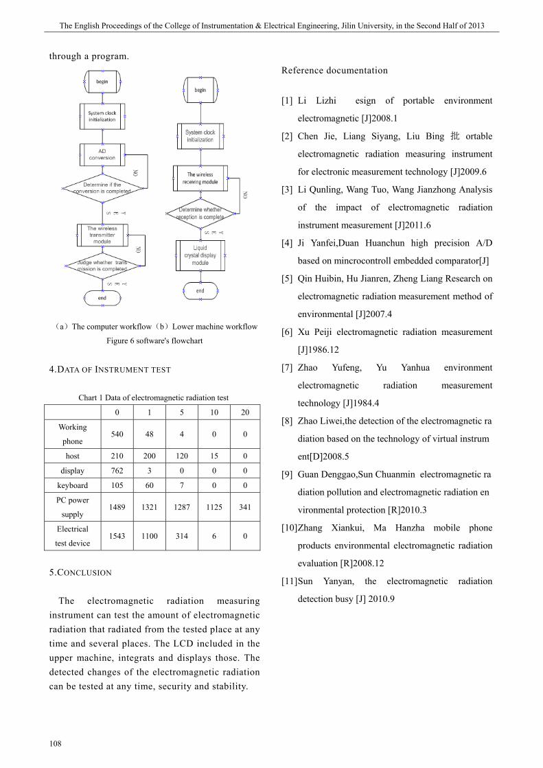
期 The English Proceedings of the College of Instrumentation & Electrical Engineering, Jilin University, in the Second Half of 2013
108
through a program.
(a)The computer workflow(b)Lower machine workflow
Figure 6 software's flowchart
4.DATA OF INSTRUMENT TEST
Chart 1 Data of electromagnetic radiation test
0 1 5 10 20
Working
phone 540 48 4 0 0
host 210 200 120 15 0
display 762 3 0 0 0
keyboard 105 60 7 0 0
PC power
supply 1489 1321 1287 1125 341
Electrical
test device 1543 1100 314 6 0
5.CONCLUSION
The electromagnetic radiation measuring instrument can test the amount of electromagnetic radiation that radiated from the tested place at any time and several places. The LCD included in the upper machine, integrats and displays those. The detected changes of the electromagnetic radiation can be tested at any time, security and stability.
Reference documentation
[1] Li Lizhi esign of portable environment
electromagnetic [J]2008.1
[2] Chen Jie, Liang Siyang, Liu Bing 批 ortable
electromagnetic radiation measuring instrument
for electronic measurement technology [J]2009.6
[3] Li Qunling, Wang Tuo, Wang Jianzhong Analysis
of the impact of electromagnetic radiation
instrument measurement [J]2011.6
[4] Ji Yanfei,Duan Huanchun high precision A/D
based on mincrocontroll embedded comparator[J]
[5] Qin Huibin, Hu Jianren, Zheng Liang Research on
electromagnetic radiation measurement method of
environmental [J]2007.4
[6] Xu Peiji electromagnetic radiation measurement
[J]1986.12
[7] Zhao Yufeng, Yu Yanhua environment
electromagnetic radiation measurement
technology [J]1984.4
[8] Zhao Liwei,the detection of the electromagnetic ra
diation based on the technology of virtual instrum
ent[D]2008.5
[9] Guan Denggao,Sun Chuanmin electromagnetic ra
diation pollution and electromagnetic radiation en
vironmental protection [R]2010.3
[10] Zhang Xiankui, Ma Hanzha mobile phone
products environmental electromagnetic radiation
evaluation [R]2008.12
[11] Sun Yanyan, the electromagnetic radiation
detection busy [J] 2010.9

Jiang Ransong etc.: The manufacture and simulation for electromagnetical damping of fiber detector
109
The manufacture and simulation for electromagnetical damping of fiber detector
Jiang Ransong Zhou Rui Xue Bixi
Abstract—With the development of the fiber shaking detector, the demand for the sensitivity and accuracy of data
collection is higher and higher, so it is a improvable direction to add a damping device to the fiber detector. When a fiber
detector receives a maximum amplitude signal, it helps reduce the amplitude in order to get prepared for the next signal. It is
necessary to design a device that can hinder the shake. It is because the structure of the cantilever is simple that it’s widely
used in fiber detector, this paper will state a damping device based on the structure of a cantilever.
The paper is divided into three parts: the background of the electromagnetic damping, the design of hardware circuit and
test, the simulation for damping device by ANSOFT and summary for the whole achievement of the project.
In the design of hardware circuit, the most important thing is to produce damping effects in closing coil after the demand
of low consumption. The paper provides three schemes: Scheme I and Scheme II are based on the electromagnetic induction
and induced electromotive force, the damping force comes from the power of the amplified electromotive force. The difference
between Scheme I and Scheme II is that Scheme I uses a trigger switch to produce the effect. Scheme II is after the
adjustment of the cantilever, using two coils. One is an induction coil, the other is a damping coil. Scheme III uses the mature
vibroswitch to control the damping coil. It makes the coil cut off when it does not shake in order to save power. In order to get
the best damping ratio, 0.707, ANSOFT becomes the simulating software. The number of a coil turns can be known from the
result of the simulation, so does the current.
Key words—electromagnetism damping; low consumption; control circuit; ANSOFT simulation
1.FOREWORD
IT is because the fiber detector has high sensitivity and wild dynamic range and it can get rid of the influence of electromagnetism, it is widely used in designs of shaking detectors. With the demand of accuracy and sensitivity are higher and higher, the usage and improvement of fiber detector is valued. So it is necessary to design a damping device that can make the sensitive device renew to the initial condition.
Now the most widely used damping devices are spring or liquid damping devices. But the spring will produce a phenomenon called metal fatigue, and damping liquid requires high and well leakproofness, so we reckon that we can use the force between intermittent duty coil and magnet to produce the damping force. This method can change the magnitude of force by changing the current, so it has advantages in adjustment than the two methods before, and it can deprive multifunction circuit to serve users. But this method needs a power supply. Consider that the device needs to be used long time in the outer
environment. We need to design a switch circuit that can switch on when the cantilever shakes and this process is automatic. So it can get the goal of low consumption in order to make the coils work longer.
2. THE STRUCTURE OF DAMPING DEVICE AND THE
DESIGN OF CONTROL CIRCUIT
2.1 The basic structure of damping device The basic structure of damping device is showed in
Figure1. When the power supply provides the power for the closing coil, it can be regarded as a electromagnet. It makes the polar N face the polar N of the magnet. And when the cantilever shakes, the probe will send a signal to the detector and with the position of the magnet and the coil is changing, the cantilever will receive a resistance and get back to the initial condition, waiting for the next shaking signal.
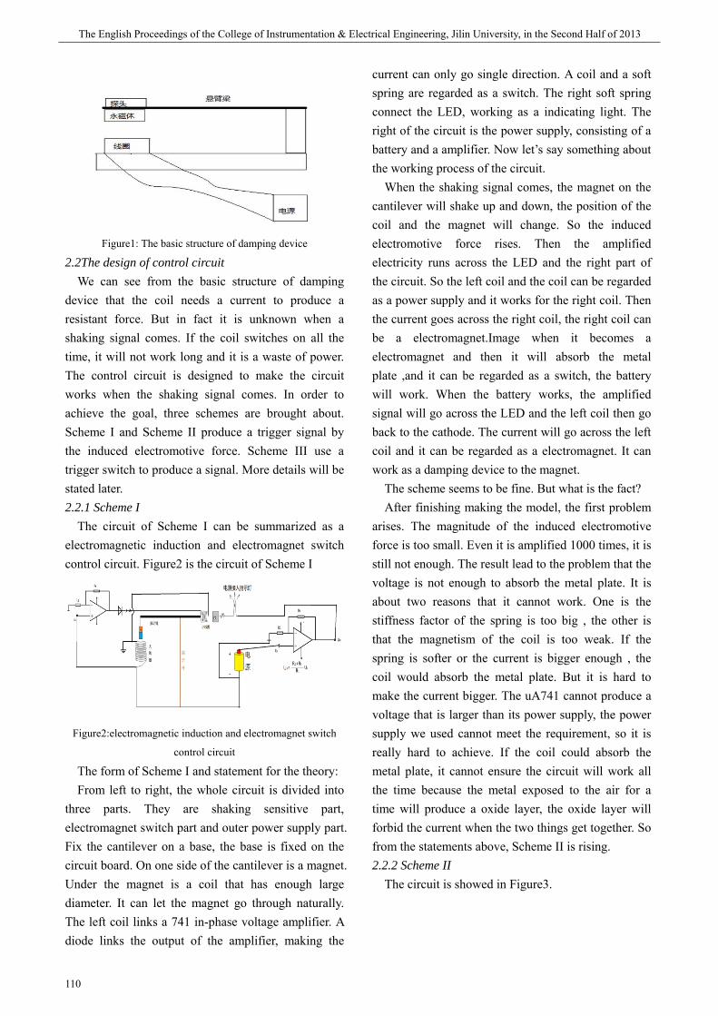
期 The English Proceedings of the College of Instrumentation & Electrical Engineering, Jilin University, in the Second Half of 2013
110
Figure1: The basic structure of damping device
2.2The design of control circuit We can see from the basic structure of damping
device that the coil needs a current to produce a resistant force. But in fact it is unknown when a shaking signal comes. If the coil switches on all the time, it will not work long and it is a waste of power. The control circuit is designed to make the circuit works when the shaking signal comes. In order to achieve the goal, three schemes are brought about. Scheme I and Scheme II produce a trigger signal by the induced electromotive force. Scheme III use a trigger switch to produce a signal. More details will be stated later. 2.2.1 Scheme I
The circuit of Scheme I can be summarized as a electromagnetic induction and electromagnet switch control circuit. Figure2 is the circuit of Scheme I
Figure2:electromagnetic induction and electromagnet switch
control circuit
The form of Scheme I and statement for the theory: From left to right, the whole circuit is divided into
three parts. They are shaking sensitive part, electromagnet switch part and outer power supply part. Fix the cantilever on a base, the base is fixed on the circuit board. On one side of the cantilever is a magnet. Under the magnet is a coil that has enough large diameter. It can let the magnet go through naturally. The left coil links a 741 in-phase voltage amplifier. A diode links the output of the amplifier, making the
current can only go single direction. A coil and a soft spring are regarded as a switch. The right soft spring connect the LED, working as a indicating light. The right of the circuit is the power supply, consisting of a battery and a amplifier. Now let’s say something about the working process of the circuit.
When the shaking signal comes, the magnet on the cantilever will shake up and down, the position of the coil and the magnet will change. So the induced electromotive force rises. Then the amplified electricity runs across the LED and the right part of the circuit. So the left coil and the coil can be regarded as a power supply and it works for the right coil. Then the current goes across the right coil, the right coil can be a electromagnet.Image when it becomes a electromagnet and then it will absorb the metal plate ,and it can be regarded as a switch, the battery will work. When the battery works, the amplified signal will go across the LED and the left coil then go back to the cathode. The current will go across the left coil and it can be regarded as a electromagnet. It can work as a damping device to the magnet.
The scheme seems to be fine. But what is the fact? After finishing making the model, the first problem
arises. The magnitude of the induced electromotive force is too small. Even it is amplified 1000 times, it is still not enough. The result lead to the problem that the voltage is not enough to absorb the metal plate. It is about two reasons that it cannot work. One is the stiffness factor of the spring is too big , the other is that the magnetism of the coil is too weak. If the spring is softer or the current is bigger enough , the coil would absorb the metal plate. But it is hard to make the current bigger. The uA741 cannot produce a voltage that is larger than its power supply, the power supply we used cannot meet the requirement, so it is really hard to achieve. If the coil could absorb the metal plate, it cannot ensure the circuit will work all the time because the metal exposed to the air for a time will produce a oxide layer, the oxide layer will forbid the current when the two things get together. So from the statements above, Scheme II is rising. 2.2.2 Scheme II
The circuit is showed in Figure3.
Jiang Ransong etc.: The manufacture and simulation for electromagnetical damping of fiber detector
111
Figure3: Coil induced voltage electromagnetic damping circuit
Now state the form of the circuit and its working theory.
The circuit consists of two branches of magnets vibrators and two connecting coils and amplifiers. When the system feels the signal from outside, the cantilever will shake with the magnets together, then the left magnet will change the position with the coil behind it, then the induced voltage arises. We can regard the left coil as a power supply when the shaking signal comes. The induced voltage will be amplified and then it can provide power for the right coil. The diode is a rectification device. The current goes across the diode then the right coil, the right coil can be regarded as a electric magnet, it can work as a damping device to the magnet above. There is a alterable resistor in the circuit. It can change the voltage that adds to the coil so that the coil can have different magnitude of magnetism.。
After several times of tests, the number of turns is 70. The resistance of the two coils is 1.8 ohm each. It is because the strength of the magnetism is related to the magnitude of the current, so the resistance needs to shut down to let the damping phenomenon more obvious. When the right coil shakes, the initial number of the voltmeter is about 1.0, maybe the 741 amplifier needs a drifting voltage. When the cantilever shakes, the number on the voltmeter begins to change regularly, the maximum can reach to 4.5 or so. This will meet the requirement to produce enough magnetism.
This image uses a thought of equivalent of power supply. The circuit makes the left coil and the amplifier a power supply to provide power to the right coil. Use the conclusion that the conductive coil is an electromagnet. It can meet the demand of low consumption.
Now let’s have a look at the volt-changeable power supply that provides power for the 741 amplifier. The left of the circuit connect to a 220V/18V transformer. It can export positive voltage and negative voltage to the amplifier. Show as Figure4
Figure4: volt-changeable power supply
Device: (1)Three terminal regulator,LM317,LM337
(2)C1 ,C2 2110 TTT ms +== , 21 TT << ,
2TT ≈ , msT 102 =
1010
01100/)(1 CIdtI
CV CI ⋅== ∫
,
AI 5.0max0 = , AI 6.00 = ,∆ VVV inI 35/1 Im == ,
uFC 20001 = C1=C2=2200uF
(3) 2V
VVVV inI 1512 Im2 ==−− δ , VV 4.132 = Define
it 18v。 (4)Design of rectifying elements (a)withstand voltage of the diode:
VVVBM 561.122 max2 =×= (1.1 is the wave of
power grid)
VVBM 90≥ , breakdown voltage is 180V
(b)maximum current of the diode:
AIIDAV 25.0)(2/1 max0 == ,
AII DAVF 45.08.1 == ,
use the 1A/200V rectifier bridge. (5)SN of the transformer:
期 The English Proceedings of the College of Instrumentation & Electrical Engineering, Jilin University, in the Second Half of 2013
112
AIIac 08.18.1 max0 == ,make it 2A。
(6)Cooling fin:
[ ] 00 *)( IVVP AV −= , WP 4.12max =
(7)According to the advice of LM317, make adjC
10uF/25v,C2 is the compensation capacitor of C1. C2 is 0.1uF ceramic capacitor ,R1=240Ω , R2 :
720Ω~2.2k potentiometer. 2.2.3 Scheme III
1) Overall design The diagram is showed in Figure5. Use the shaking
signal from the vibroswitch to link to delay-circuit can provide power to the coil. Then begin to time. It can show the magnitude of voltage when the coil on or off. When the time is up, the coil will cut off. It needs a single chip to control. Like ADC0804, NE555 and so on. These chips are wildly used in toys and alarm systems and control circuit. And the device designed is the combine of these things and serve the cantilever damping device.
Figure5 The diagram of the system
2)The choice of the elements and applications in circuit
(1) Information of SW-420 Now a lot of vibroswitches can be bought. This kind
of switch can close when it feels the shaking signal and it is really cheap. It also has simple structure and it is widely used in many fields. It can be seen as spring switch and ball switch. The two kinds have important features. They are sensitivity and directivity. The so called sensitivity is that the different switches have a difference. Users can choose different kinds of switches when they want to use them in different situations. Directivity is the forced direction. Most products have the requirement in sensitivity but not in directivity. So there is a need to know something about how the users use them then decide which to choose. The difference between the two kinds of switch is the
way they feel the signal. The sensitivity of the ball switch is the detection angle. It can start the circuit.
Choose sw-18020 and sw-420. But in fact, sw-18020 is likely to be broken sometimes, so finally choose sw-420. It is more safe and stable.
Spring switch
Ball switch
Figure6 Switches
Finally choose a sw-420 .It has a potentiometer to change the sensitivity and a LM393 to ensure is can produce stable wave. The product produces a high level when the shaking signal comes while it produces a low level when it does not feel the signal.
(2) The relay drived by the audion sw-420 has a large resistance, the driving current is
more than 10mA.If put coil directly into the coil will cause the problem that it cannot have enough current so that the magnetism will too weak. So it is necessary to add a audion to drive the relay in order to produce enough magnitude of current.
According to the theory, the current in the coil should be two times than the base of the audion. Choose the 1N4001(25V).
The
switch
produces
a signal
The delay
circuit
starts to
work
Drive circuit and
the load
Display

Jiang Ransong etc.: The manufacture and simulation for electromagnetical damping of fiber detector
113
Figure7: The relay drived by the audion
The circuit needs a 5V power supply. Add a 100ohm resistor to the base, choose the s8050npm to be the audion, relay has six feet, 5V.
(3) The circuit shows the voltage of the coil In order to adjust the current better and know the
state of the coil, we can use a display screen to show. It is measured the resistance of the coil is 64.2ohm. Use ADC0804 to transform.
(3-1) STC89C52 STC89C52 is a product of STC. It has 8K
programmable flash storage. STC89C52 use MCS-51 as its core and has many improvements that 51 singlechip does not have. It has 8bit CPU and programmable flash storage. It has these functions: 8k bit flash storage,512bit RAM, 32 bit I/O, timer ,inside 4KB EEPROM,MAX810circuit,three 16 bit timer/counter,4 outside interrupt,a 7 sides 4 class interrupt structure.
Figure8: STC89C52
Figure9: ADC0804
Chip parameter:working voltage:+5V, VCC=+5V
Analog input voltage range:0~+5V,0≤Vin≤+5V
Resolution ratio:8 bit,1/2=1/256
Transform error:±1LSB
reference voltage:2.5V, Vref=2.5V
(3-2) ADC0804 transformation ADC0804 is a successive approximation method
A/D transformer,this kind of A/D transformer has not only its speed is fast, but also revolution ratio is high and its price is cheap. It is widely used in design of microcomputer ports.
Take a 8 bit ADC0804 as an example: The 1st result:10000000 (if assumption≤input,
searching bit=assumption bit=1) The 2nd result:11000000 (if assumption≤input,
searching bit=assumption bit=1) The 3rd result:11000000 (if assumption>input,
searching bit=assumption bit=0) The 4th result:11010000 (if assumption≤input,
searching bit=assumption bit=1) The 5th result:11010000 (if assumption>input,
searching bit=assumption bit=0) The 6th result:11010100 (if assumption≤input,
searching bit=assumption bit=1) The 7th result:11010110 (if assumption ≤input,
searching bit=assumption bit=1) The 8th result:11010110 (if assumption>input,
searching bit=assumption bit=0) Use the way as dichotomy,8 bit A/D transformer
needs 8 times of searching, 12 bit needs 12 times of searching, then will finish the task of transformation. The inputs stands for the analog voltage in Figure5.
The functions of some feet: D0-D7:numbers output, the result is expressed in
binary numbers CLK:offer the pulse signal, fCK=1/(1.1×R×C) CS:Chip selection
期 The English Proceedings of the College of Instrumentation & Electrical Engineering, Jilin University, in the Second Half of 2013
114
WR:Write RD:Read INTR:Interrupt; Other feet are showed in Figure8 and Figure9. (3-3)Programming and proteus simulation
Figure10: AD display and proteus simulation
Program: #include <reg52.h> #include <delay.h> //#include <intrings.h> //#include <stdio.h> #include <adc0804.h> #define uchar unsigned char #define uint unsigned int sbit adwr=P3^6; sbit adrd=P3^7; uchar code table[]=0x03,0x9f,0x25,0x0d, 0x99,0x49,0x41,0x1f, 0x01,0x09; void display(uchar bai,uchar shi,uchar ge) P2 =0X20; P0=table[bai];DelayM(5); P2 =0; P2 =0X40; P0=table[shi];DelayM(5); P2=0; P2 =0X80; P0=table[ge]; DelayM(5); P2 =0; main() unsigned int aa,bb; while(1) aa=adc0804(); bb=aa;
display(bb/100,bb%100/10,bb%100%10); After several times of adjustments and
improvements, finally get the target. 0-5V voltage on the coil is showed in numbers range 0 from 255.
(4) Design of 555 delay circuit 555 circuit is a widely used integrated circuit.
Because it has high sensitivity, we need to take some action to protect it from being disturbed, take the circuit showed in Figure7 as the final circuit. The circuit is based on 555 and add switch made by transistor and a self-lock circuit.
Figure11: 555 delay circuit
Analysis about the working process of the circuit: The circuit consists of a 555 pulse-launched model,
its output connects a control relay. The process is when it outputs a high level, the relay is absorbed. When it outputs a low level, the relay is released.
Pin2 is the trigger pin. It is triggered by low level. Usually the 555 circuit is triggered by pin2 and it is launched by a resistor R4. Pin3 outputs a low level, the delay is released. When the switch is touched, the power supply provides the power by R1 to the base of SCR, making it switch on. It produces a negative pulse when the base turns from high level to low level. The negative pulse trigger the circuit by a 0.1uF conductor, making the circuit turn. The relay is absorbed because pin3 outputs a high level.
(5) Modules debugging Exact information is not found about the process.
Mainly depends on every withstand voltage and current data of each device, attempt using different resistor to the circuit. The first step is the combination of the vibroswitch and the delay circuit. We can directly connect the output pin of the vibroswitch to the delay circuit because the driving current of the vibroswitch is larger than the minimum of audion base
Jiang Ransong etc.: The manufacture and simulation for electromagnetical damping of fiber detector
115
current. The second step is the combination of delay circuit and the load. Information shows that when delay circuit is in transient state, pin3 outputs high level and more than the driving current is more than 200mA. Then decide to add delay coil , but it could not work normally. The voltmeter shows that it is about 5V in pin3, so maybe the current is not enough. Finally it succeeds. And the whole combination work is done. After adjusting the sensitivity of the vibroswitch then connect the power supply, it meet the requirement that is said before. Please look at Figure12 and Figure13.
Figure12: Test result(before shaking)
Figure13: Test result(after shaking)
2.2.4 Comparison among the schemes From the three schemes showed above, Scheme I
and Scheme II have a lot in common. The two scheme both use the theory that the process of induced electromotive force to produce the damping phenomenon. But there is still a difference. That is Scheme II directly uses the amplified induced voltage to be the supply of damping circuit. From the comparison above we can conclude Scheme II has some advantages. The first advantage is it has a better feasibility. In Scheme I we only think about the coil will be a magnet when it meets current, but ignore the important fact that it depends on the magnitude of the current. So it cannot absorb the metal plate. The
second advantage is in Scheme II it directly uses the amplified voltage without any middle links. The third advantage is Scheme II is more energy-efficient. It does not use a battery.
Data is showed in list 1 List 1: Data of Scheme I and Scheme II
NO.1
circuit
turns
NO.2
circuit
turns
Maximum of
induced
voltage
Resistance of
NO.2 circuit
Scheme
I 70 60 4.5V or so 1.2ohm
Scheme
II 70 70 4.5V or so 1.8ohm
Scheme III use the vibroswitch, so it is more stable. It has more simple structure than Scheme I and Scheme II. And it use delay circuit, display circuit and reasonable ways to control the coil and the switch. So it has the good result. The voltage of the coil is showed on the screen so it is easy to see the state of the coil.
3.SIMULATION
3.1 Sketch of system simulation The fundamental of fiber detector is to fix the
detector on the cantilever, get the shaking signal by vibrating reed. Inlet the fiber signal on the other side at the same time, meanwhile producing different light wave by the influence the signal acts on the reflector plate. Measure it and then get the data, calculate the data we need. The damping part is really important. Only when the damping ratio reaches to 0.707 do we receive the well shaking signal. In order to analyse the damping ratio, first we need to simulate the stress of the magnet in closing coil. Frequently-used magnetic field simulation software are ansys,matlab,ansoft and so on. After comparison we choose the ansoft.
Ansoft Maxwell 2D/3D is a powerful, precise and easy soft from Ansoft company. It includes electric field, magnetostatic field, vortex field, transient field and temperature analysis module. It can analyse the static state, steady state, transient state, normal condition and trouble condition of electrical machine, sensor, transformer, permanent device and exciter. It has UI from top to bottom, banner adaptive mesh generation technic and uses definition database, making it has better usability. It also has the capacity
期 The English Proceedings of the College of Instrumentation & Electrical Engineering, Jilin University, in the Second Half of 2013
116
to use high-performance matrix to provide the fastest speed.
Ansoft has some advantages: 1. It has perceptual intuition friendly GUI, quick and exact self-adaption solver and powerful post-processing function. 2. It has a whole simulation design environment, it can simulate force, torque, capacitance, inductance and energy. It can also draw scalar potential, electric field intensity, magnetic line of force, field density and energy in cloud picture, vector diagram or isoline.3.Powerful and flexible macros can alter the modules conveniently and has the function of parameter analysis. 3.2 To simulate the force of the magnet by ansoft
The initial model choose the coil’s diameter is about 10mm, 33mm height. When it comes to the simulation, choose the polyhedron that has 36 surfaces. The diameter is 10mm and the height is 33mm. This kind of simulation ensures that they have similarity and it is simple for the software to simulate the model. Then choose copper to be the material. Choose the profile then apply an electric current to finish the simulation. It is also OK to use a cylinder to simulate, but there is a problem for the computer to work because it needs a long time to calculate, maybe it could not calculate correctly.
Choose a cuboid that has the same size as used in the model. Choose the Z coordinate to be the variable. Make its moving distance is close to the real moving distance. Choose the material as NdFe30. Set the parameter as its stress. The fundamental model is showed in Figure14.
Figure14: Model of damping device
When finish all the sets above , we can get the relationship between the stress and the Z coordinate of
the magnet. Look at Figure15 and Figure16. The stress is showed in y axis, the unit is N. The Z coordinate is showed in x axis, the unit is mm.
Set the unit of account to be 0.5, showed in Figure15. When make it to be 0.1mm, showed in Figure16. There is some disturbance because there is a induced voltage. It is necessary to get rid of them. Some data is showed in List2.
Figure15: The relationship between the stress and the Z
coordinate of the magnet
Figure16:The relationship between the damping force and the Z
coordinate
List2 Information of Z coordinate and the damping force
It can be easily seen from the data that the maximum of the damping force is when the bottom of the magnet meets the top of the coil. That is to say, when z=33mm, F comes to the maximum 1.52907N. When Z is not more than 33mm, the magnet goes into
Jiang Ransong etc.: The manufacture and simulation for electromagnetical damping of fiber detector
117
the coil and the stress gets smaller. When Z is more than 33mm, the magnet leaves the coil farther and farther, the damping force gets weaker and weaker. It agrees with what we learned. The error of the simulation is in the allowed band. 3.3 Analysis to the result of the simulation
In the physics and engineering science, the mechanical model of a damping force is in direct proportion to the velocity of shaking and it is a force that has inverse force with the direction of the shaking. The model is called stickiness damping model. It is the most widely used model. It can simulate the damping function of air, water or other liquid well. Now mainly discuss the model of stickiness damping device. It is necessary to point out that there are many damping machine-made that still not exit in nature, such as a shaking spring on a desk that has a constant friction factor. The stress is related to its weight and the friction factor but not the speed. Besides the simply shaking damping force, electromagnetic damping, media damping, structure damping are also concrete forms of damping. Although now scientific community has put forward many kinds of mathematical models for damping, it is hard to choose the model when we come back to reality. So let’s explain it in details.
Viscous damping can be expressed as the following formula:
(3.1) F stands for the damping force. V is the velocity of the vibrator. C is a constant represents the magnitude of damping. The unit is N/m. These relationships is similar to the Ohm’s law. It is easy to see some examples of damping in our daily life. For example, use your hand to touch the chord, then the sound will fade out. The tree will stop shaking after the wind. A damping phenomenon is one of the most common things. An ideal spring damping device is showed in Figure17. Forces we want are elastic force(k is stiffness factor. X is the displacement )
Fs = − kx (3.2) Damping force (C is damping factor, v is the
velocity of the vibrator ):
(3.3)
Imagine the vibrator does not suffer from any force
outside, then write the oscillation equation with the help of Newton’s Second Law:
(3.4)
A is accelerated speed. In this project, we use the induced voltage to
produce the force to achieve the damping phenomenon. But the information searched before is mainly about viscous damping. They are not useful. So it is necessary to calculate again to build a new way to solve our problem.
In viscous damping model, the relation is . But in our own model, the result is
showed in Figure16. There are two ways to build the model: Scheme I: Use the curving fitting to draw a
Gaussian distribution curve. Suppose the relationship between F and x is
2( )x BF Ae− −= (3.5)
A and B are constants. The advantage of this scheme is it is close to the real curve of F and x. Disadvantage is it’s not good for the following calculation.
Scheme II: Match on the both side of the peak:
11F xk B= +
(3.6)
22F xk B= +
(3.7)
The advantage of this scheme is it is good for the following calculation. Disadvantage is there is a error with the primitive curve.
Now calculate Scheme II. The force is showed in Figure17.
Figure17: Force of the magnet
+ -GF FF =合 拉 阻 (3.8)
= *F k x拉 拉 (3.9)

期 The English Proceedings of the College of Instrumentation & Electrical Engineering, Jilin University, in the Second Half of 2013
118
a=mF合
(3.10)
2 2
t 0- =2asv v (3.11)
We get:
2 11t
2* + - 2* * + -2* *x= = =
m m mF G *xF G *xkv
x xk BF +阻拉 拉合
(( ) )
(3.12) So:
221 1 1 t
1
( ) 2*( )* *
2( )vk
kG G m
x kB Bk
− ± − − +=
+拉
拉
(3.13) From formula(3.6),so
221 1 1 t
111
( ) 2*( )* **
2( )vkF k
G G mkB Bk Bk− ± − − +
= ++
拉
阻
拉
(3.14) Analogy from viscous damping system,
(3.15)
And formula(3.1),we get
11
mc= *2( )kk k+拉 (3.16)
This is the damping factor relation of electromagnetic damping So
11
21 1 1
111
m*2( )
=( ) 2*( )*
2* *2( )
kk
kG G m
k kkB Bk Bk
ς+
− ± − − ++
+
拉
拉
拉 (3.17) After simplification,
11
*
*
mkk k
k mς
+= 拉
拉 (3.18) The formula is the formula of damping factor. The difference of two schemes is the formula of
F阻 . As to Scheme I, from formula(3.5) and
formula(3.11), we know: 2( )
2
t
2* + - 2* * + -2* *x= = =
m m mF G *xF G *xkv
x Bx AeF − −阻拉 拉合
(( ) )
(3.19)
This equation is hard to solve, we can only use matlab to calculate. So only solve Scheme II. Use the image of the stress of the magnet to fit a straight line, here is the data:
List3: The relationship between x and y from Figure16
unit:mm X Y
Team 1 33.2 1.689487
Team 2 33.4 1.465038
Team 3 33.9 0.791161
Team 4 34.6 0.510709
Team 5 35.0 0.399476
Team 6 35.5 0.220396
Team 7 35.6 0.110591
Team 8 35.87 0.071676
After calculation,
34.6125x = ,0.6573y =
From 2 2( )X x x= − ,we get the following list
List4: The variance that used in matching
2X Team 1 1.9951
Team 2 1.4702
Team 3 0.0126
Team 4 0.0002
Team 5 0.1502
Team 6 0.7877
Team 7 0.9752
Team 8 1.1827
Then can calculate xy, look at List5.
So,2 6.5739X =∑
4.1253xy = −∑
After calculation the straight line is
22.3766 0.6275y x= −
From the formula(3.18),we get
11
*0.1324
*
mkk k
k mς
+= =拉
拉 . It is not hard to know that the damping ratio cannot
reach the requirement of 2
2. It indicates why the
damping phenomenon is not obvious.
Jiang Ransong etc.: The manufacture and simulation for electromagnetical damping of fiber detector
119
List5: Some results
xy
Team 1 -1.4580
Team 2 -0.9293
Team 3 -0.0954
Team 4 0.0018
Team 5 -0.0799
Team 6 -0.3877
Team 7 -0.5399
Team 8 -0.6369
4. CONCLUSION
The paper put forward a thinking of designing the damping device for the fiber detector and designs three schemes. After testing every scheme, we get every result of the tests , feasible conclusion and ways to improve. As to Scheme I, because the material and the way we did is not totally correct, and the limit of induced voltage, it is hard to finish the task. Scheme II still uses the induced voltage to be the trigger signal and change the structure. It is more feasible than Scheme I. The result is that the amplified induced voltage is about 5V. But the damping phenomenon is not obvious. It can be improve by changing the turns of the coils. Scheme III use the vibroswitch and relay-drived circuit, 555 delay circuit and AD display circuit. It finally finishes the task by feasible combination. The damping force can be changed by adjusting the potentiometer. Time-lapse can be changed by adjusting the potentiometer of RC circuit. It ranges from 0—25s. The whole circuit meets the requirement of low consumption, making it closer to put into use in daily life. The circuit is simple and stable. But in the limit of material, it does not have an ideal size.
And in addition, solution to the disturbance of weak induced voltage when the coil and the magnet have inter motion has not been thought of yet. In simulation, we know the relationship between the stress of the magnet and the Z axis coordinate, then use the least square method to simulate. We get the relationship of the force and Z coordinate. Next according to the information of viscous damping, we deduce some mathematical formulas towards the damping force. In order to ensure the formulas are right, we calculate the
data of our own model. The result shows the formulas are believable. We can get some parameter from the optimized damping structure and can adjust the parameter of our model to make it work better. Finally we set a good base of designing other parts of the fiber detector.
References
[1] Li Xuecheng The research based on FBG seismic
sensor[D] Lanzhou: Lanzhou University, 2010.
[2] Liu Hanping, Wang Jiangang, Cui Hongliang,
Chen Bingquan. FBG earthquake detector[J].
Shandong University college journal. The 37th of
2nd periodical, 89-90.
[3] Zhang Hongrun, Fu Jinxin. 200 examples of
application of sensor[M]. Beijing; Beijing
university of aeronautics and astronautics
press,2006: 299-303.
[4] Kang Huaguang. Electronic technology
foundation for analog parts[M]. The 5th edition.
Beijing: Higher Education Press,2006: 144-147.
[5] Guo Tianxiang. C language for New Concept 51
Singlechip [M]. Beijing: Electronic Press. 2009:
95-110.
[6] Li Xuehai. Fast Practice for Classic 80C51
Singlechip[M]. Beijing: Tsinghua University
Press,2012: 11.
[7] Xiao Jinghe. Selection of 555/556 integrated
circuit[M]. Beijing: China Electric Power Press.
2010:42-44.
[8] Song Zhiying. Temperature alarm circuit of
NE555[J]. Experimental technique and
management. 33-35.
[9] Sui Tao. A design that can control delay
circuit[J].Coal mine modernization. The
69th :41-42.
[10] Chen Hong, Hou Guodong. Electromagnetic field
analysis and simulation for long straight

期 The English Proceedings of the College of Instrumentation & Electrical Engineering, Jilin University, in the Second Half of 2013
120
solenoid.[J] Light Engineering Institutes of
Zhengzhou.
[11] Liu Guoqiang, Zhao Lingzhi, Jiang Jiya. Ansoft
finite element analysis for engineering
electromagnetic field[M]. Beijing: Electronic
Industry Press.
[12] Jiang Desheng, Chen Daxiong, Liang Lei. The
adhibition of ANSYS in design of fiber Bragg
raster accelerometer[J]. 2004 23 11th.
[13] Lv Gonghe. Theory and features of seismic
exploration detector and relative analysis[J].
petroleum exploration. 2009, November 48th of
6th periodical.
[14] Liu Hanping, Wang Jiangang, Cui Hongliang,
Chen Bing. FBG earthquake detector[J].
handong University college journal. The 37th of
2nd periodical.
[15] Li Xiangsheng. Active control and simulation of
electromagnetic damping suspention[J].
Agricultural machinery,2004.
Wang Duoqiang etc.: Intelligent House Leakage Detection and Alarm System
121
Intelligent House Leakage Detection and Alarm System
Li Suyi, Wang Duoqiang, Bai Yang, Zhang Weijie
(College of Instrumentation & Electrical Engineering, Jilin University. Changchun, Jilin, China) Abstract—This study designs a kind of discontiguous reflected liquidometer system which has the characteristics of low cost,
high-resolution, high sensitivity and high anti-interference capability. It fits for the minimum liquid height and can be applied
to the house-leaking. The photoresistances that are linear set on the liquidometer are used to receive the laser signal to
improve the resolution. The discontiguous reflected liquidometer system consists of sensor, MCU, GSM and power supply.
The hardware circuit design, software design, detection principle and testing result are introduced. By data analysis we can
get the conclusion: sensor resolution 3mm, average error 0.19mm, standard error 0.51mm. This system can measure several
kinds of house-leaking and run normally at least 72 hours.
Key words—house-leakage, discontiguous, reflected, GSM, liquidometer
0. INTRODUCTION
THE house-leaking happens frequently and causes property loss especially in apartment. It may cause other secondary disaster such as fire, electric shock and short circuit. The technology about intelligent alarm system is mature but lack for a kind of system that is cheap and high-resolution. In order to solve the problem, we develop a system that can measure the liquid level fast, accurately, conveniently and can be used in ordinary family.
There are several detection methods to measure the liquid level: sonic detecting technique[1], liquid short-circuit method, flow detection method, Magnetic Float Gauge[2] and Diffused Silicon Pressure Transducer technique[3]. But all of these instruments must contact the liquid directly that can be covered by the dirt leading to the inaccurate measuring result.
And the majority of current non-contact liquid level detection devices use ultrasound as propagation medium. The devices always get bulky, expensive, complex and can’t be used in common family. Although the non-contact level detection method[5] based on the refraction of light can achieve the aim, the liquid which is measured must be transparent and depends on the optical imaging lens. In order to achieve the rise or fall of the water level , the linear array CCD [6] or the linear arrangement of fiber optic sensors [7]is used, so that the detection resolution is
improved, but the cost is greatly increased. In conclusion the contacting liquidometer has the
defect of easy hanging dirt, short working life, high price etc. And the caustic liquid can’t be measured. The refracted detection equipment can only measure the transparent fluid and depend on the optical imaging lens and its anti-interference capability is weak. In order to overcome the defect talked above, this study designs a kind of discontiguous reflected liquidometer system which has the characteristics of low cost, high-resolution, high sensitivity and high anti-interference capability.
The application of GSM technology makes it possible to detect the house leakage and alarm in distance when no one in the house. Once the water-level changes, the system can measure the signal immediately and send the alarm message to the user’s mobile phone.
1. HOLISTIC STRUCTURE
The holistic design is shown in Figure 1, the system is consist of discontiguous reflected sensor, MCU, GSM, LCD screen and power supply(is not shown in the figure). The output of the discontiguous reflected sensor is connected to the MCU input, the outputs of the MCU are connected to the LCD screen and the GSM. The sensor will send the water-level information to the MCU when it detect the water. Then the MCU module classifies and treat the
期 The English Proceedings of the College of Instrumentation & Electrical Engineering, Jilin University, in the Second Half of 2013
122
information to judge the water-level and control the GSM to send alarm message. The LCD screen display the water-level instant.
Figure 1. Fundamental Structure
2. THE HARDWARE DESIGN
2.1 The design and manufacture of the discontiguous reflected sensor.
Seen in Figure 2, the schematic diagram shows the theory of the discontiguous reflected sensor: when the laser diode send laser toward the liquid surface as a certain angle, the reflection happened. The reflected laser spot will move toward the laser diode parallelly as with the rising of the liquid. On the other hand, if the liquid level drops, the laser spot will move closer to the laser diode parallelly. The photoresistances are set on the trajectory of the spot linearly to perceive changes in light intensity. By measuring the logic level of the photoresistances, we can know the difference of the liquid level.
Figure 2. Collecting Theory
However, the diffuse reflection of the laser and other light source cause interference so that the photoresistance can’t be used as the device to measure the liquid individually. To meet the requirements of the high-resolution, high sensitivity and high anti-interference capability, the receiving pipe is used. It obviously improves performance that is required and can be applied to detect the house leakage. The photoresistance is mounted in the receiving pipe to dampen the interference caused by the diffuse reflection of the laser and other light source so that the anti-interference, resolution is improved and the resolution ratio has reached 1 mm. The figure 3 is the discontiguous reflected sensor design drawing.
1.Plastic casing 2.Laser source 3.Receiving pipe
4.Photoresistance
Figure 3. Light reflex non-contact liquid level detection sensor
module schematic diagram
2.2 The MCU Control Module Figure 4 is the schematic diagram of this module.
As shown in figure 4 α is the angle of incidence, H is the height of the equipment, h is the water-level, L is the length of the apparatus, x is the displacement of the laser spot on the sensor.
Figure 4. Signal Processing Module Calculation Principle
Diagram
The formula derivation process is as follows: tan α= (L / 2)/H (1) tan α= (x / 2)/h (2) x= (L/H) h (3)
By geometric analysis we can get: x=(L/H)/h . The distance of the laser spot is decided by height of the equipment, water-level, the length of the apparatus. Once x is known, the water level is detected.
In order to detect the water level in time, this design uses a linear array of photoresistance array and receiving pipe to receive laser signal. The resistance(10 kΩ)is in series with photoresistance to low down voltage. If the photoresistance is illuminated by laser, the MCU will receive low level form the I/O so that we can know the distance of the laser spot and the water level. 2.3 GSM sending module
Through market research, we have chosen SIM300 GSM SMS module which is consumption and widely used. Just insert a SIM card when using the module to the module slot. If the system start, GSM SMS sending module will wait for the alarm signal, when the water level changes controlled by the MCU to
Wang Duoqiang etc.: Intelligent House Leakage Detection and Alarm System
123
send alarm SMS.
3. SOFTWARE DESIGN AND IMPLEMENTATION
Software design of the system is consist of signal processing and SMS module. 3.1 The software of signal processing
This section consists of two programs: Firstly, the initialization of I/O port and interrupt are
defined, and then enter the main loop. The program in the main loop is used to display the water level at the time and detect changes. It will send water level signal immediately once water level increase or decrease, simultaneously start the message counter. The program continues to display water level if there is no change of it.
When the level changes, program start scanning from the furthest photoresistor away from the laser source. If low potential signal is detected, the alarm signal is generated and read out the current level. At the same time the system stops the scanning. If high potential signal is detected, illustrating there is no laser spot. The system continues scanning until the first high is detected. After the water level signal is sent the program will restart the c\scanning. Loop detection is achieved.
Figure 5. Signal Processing of The Software Design
This program uses the 60ms timer interrupt, the interrupt subroutine count 6s (used for experiment, it can be adjusted ). Whenever the interrupt is triggered, the SMS counter is checked. If the value is less than or equal to 2, program sent to the GSM module to send message and the message counter plus 1. Otherwise, immediately disable interrupts. The specific process is shown in Figure 5. 3.2 SMS software design
MCU control the GSM module through the serial port. The procedures of this paragraph by the operating instructions of the GSM communication module AT command manual [13] query.
Figure 6. SMS Sending Part of The Software Design
First, the LCD display module, single-chip control module, and GSM SMS sending module is initialized. After the successful launch of the GSM module system enters detecting water cycle. Secondly, GSM module extracted from the single-chip serial I/O signal sequence length of three. If a "000" is returned the microcontroller continues to detect, otherwise wait. If the I/O signal sequence is maintained for a period of time and then becomes "000", meaning checksum is
期 The English Proceedings of the College of Instrumentation & Electrical Engineering, Jilin University, in the Second Half of 2013
124
correct, the I/O signal sequence is valid, otherwise invalid. Finally, the MCU identify the I/O signal sequence content to determine the corresponding water level and control the GSM module to send alarm SMS. After the sending of the alarm message the program continues to detect code circular. Software process is shown in Figure 6.
4. PROTOTYPE TEST AND ERROR ANALYSIS
The fluctuation of the liquid surface will produce errors. The liquid level is likely to produce a level change of 1mm while measurement, in order to enable the detection and alarm system to be stable and reduce the false alarm or alarm frequently the water level is divided into 6 level, each level interval 3mm. As the level increases, reaching the corresponding level, LCD
screen will display the current level (display 0 when there is no water), at the same time GSM module will send an alarm SMS to the users’ phone. 4.1 Laboratory Instrument
Sink, Homemade home flood alarm system, caliper. 4.2 The measurement of the accuracy and resolution . 4.2.1 Measurement method
Inject the liquid into the sink slowly, stop the injection while the LCD screen displays the level variation, the current level is measured with a caliper and recorded. Continue to inject water until it reaches level 6. Through this method, 10 groups of measurement data as shown in Table 1, error analysis are shown in Table 2, which Δh is the difference between the measured value and the actual value of the unit mm.
Table 1. Measurement data table
actual value measured value Δh actual value measured value Δh actual value measured value Δh
1.00 1.00 0.00 4.00 4.00 0.00 7.00 6.80 -0.20
1.00 1.20 0.20 4.00 4.20 0.20 7.00 7.10 0.10
1.00 1.20 0.20 4.00 4.10 0.10 7.00 7.10 0.10
1.00 1.10 0.10 4.00 4.20 0.20 7.00 6.90 -0.10
1.00 1.10 0.10 4.00 4.20 0.20 7.00 7.00 0.00
1.00 1.20 0.20 4.00 3.80 -0.20 7.00 7.10 0.10
1.00 1.00 0.00 4.00 4.00 0.00 7.00 7.10 0.10
1.00 1.10 0.10 4.00 4.10 0.10 7.00 7.10 0.10
1.00 1.10 0.10 4.00 3.20 0.80 7.00 1.90 0.90
1.00 1.20 0.20 4.00 4.90 -0.10 7.00 6.90 -0.10
10.00 9.80 -0.20 13.00 12.70 -0.30 16.00 15.90 -0.10
10.00 10.00 0.00 13.00 12.60 -0.40 16.00 15.80 -0.20
10.00 9.20 -0.80 13.00 12.20 -0.80 16.00 16.20 0.20
10.00 9.70 -0.30 13.00 12.80 -0.20 16.00 15.50 -0.50
10.00 9.70 -0.30 13.00 12.90 -0.10 16.00 15.80 -0.20
10.00 9.80 -0.20 13.00 12.90 -0.10 16.00 15.90 -0.10
10.00 10.20 0.20 13.00 13.40 0.40 16.00 16.20 0.20
10.00 9.80 -0.20 13.00 13.20 0.20 16.00 16.40 0.40
10.00 10.20 0.20 13.00 13.20 0.20 16.00 16.00 0.00
10.00 9.70 -0.30 13.00 13.00 0.00 16.00 15.90 -0.10
Table 2. Error analysis table
actual value average
error
standard
error actual value
average
error
standard
error actual value
average
error
standard
error
1.00 0.12 0.14 4.00 0.13 1.30 7.00 0.10 0.32
10.00 -0.19 0.35 13.00 -0.18 0.15 16.00 -0.04 0.26
4.2.2 The measurement results According to Table 2, the average of average error
-0.01mm; the average of standard error - 0.42mm. The measurement can be approximated with an
Wang Duoqiang etc.: Intelligent House Leakage Detection and Alarm System
125
average error of 0.01mm; standard error of 0.42mm. Gaussian theory of accidental error shows that 68.3% of the measurement error is between 0.42mm. 4.2.3 The system false alarm rate experiments
i . Detection Method: Under laboratory conditions, simulate no water,
water seepage (smooth flow), the leakage (medium flow rate of water flow), water pipes burst (turbulent flow) four cases. Detect the alarm system whether works normally under these four cases . Different alarm system live to work 72 hours to observe the stability.
ii . The test results: No leaking: don’t send alarm SMS . System false
alarm rate equals 0. iii . Leaking: water seepage, leakage and water
pipes burst in the three different situations can send alarm SMS properly.
5. CONCLUSION
This study designs a kind of discontiguous reflected liquidometer system. The system is applied to design the alarm for house-leaking. The innovative use of the linear array of photosensitive resistor as the light receiving member, not only improves the resolution and accuracy, but also reduces the cost. The experiments show that the system is suitable for domestic use low-cost, long-range flood alarm system.
6. ACKNOWLEDGEMENTS
This project is supported by the Jilin University. Special thanks to Ms. Li Suyi of College of Instrumentation & Electrical Engineering, Jilin University, for their invaluable assistance in the design suggestion. The author also thanks to College of Instrumentation & Electrical Engineering, Jilin University.
References
[1] Liu, Zhiqiang & Sun, Yujing. Application of Sonic
Detecting Technique in Regional Water Leakage
Detection [J]. WATER TECHNOLOGY. 2009,
3(1):47- 49.
[2] Zhang, Feng. Magnetic Sub-level of Design and
Installation [J]. Meter Sensor .2001.1:42-43.
[3] Ning Rulong. Invested Diffused Silicon Level
Gauge Principle [J]. ZI DONG HUA YU YI QI YI
BIAO. 2000. 4:51-52.
[4] Wang, Hongbo. Chen, Xi. Qian, Lisha & Zhou,
Leijiao. Non-contact Ultrasonic Level
Measurement Method [J]. Fujian Computer. 2011.
2:11-12.
[5] Gao, Yue. Refraction of Light Non-contact Ype
Liquid Level Monitoring Device and Use the
Device Detection System. China Patent: CN
201600171U [P]. Announcement Date: 2010.
10.16.
[6] Wang, Weiqiang. Linear CCD Level Measurement
and Optical Path Design [D]. Harbin Engineering
University. 2011. 3.15.
[7] Huang, Yanping. Pei, Li & Jian, Shuisheng.
Description on optical fiber liquid level sensor
(OFLLS) [J] Optical Communication Technology.
1995. 2:131-136.
[8] Zhan, Yang. Variable Condenser Water Level
Switch [P]. Chinese Patent: CN201869184U,
2011-06-15.
[9] Sun, Qingdian. Li, Canxin & Cheng, Yong.
Research and Design of Water Supply Pipeline
Leakage Warning Monitoring Device [J]. Water
Resources and Power .2010, 28 (10): 125 - 127.
[10] Yu, Hongbo. On the Leakage Alarm System [D]
Beijing: National Library of The Center of the
Fire Control Room.2006.
[11] Li, Yuan & Tie, Yong. Water Leakage Detection
Algorithm Based on LMS Denoising Algorithm
[J]. Journal of Inner Mongolia University. 2008.39
(2): 172 - 176.
[12] Yu, Qixiang. Leak-proof Safety Lock and Water
Leakage Alarm Systems [P] China Patent:

期 The English Proceedings of the College of Instrumentation & Electrical Engineering, Jilin University, in the Second Half of 2013
126
CN202329950U.2012-07-11.
[13] AT Command Manual

Yuan Guiyang etc.: Office computer displayer of electromagnetic radiation measure and alarm system
127
Office computer displayer of electromagnetic radiation measure and alarm system
Yuan Guiyang;Shen Chunyang;Liu Gucheng
(College of Instrumentation and Electrical Engineering,Jilin University,Changchun 130012,China) Abstract—In this paper,a STC89C52 MCU based portable office computer display of electromagnetic radiation measuring
instrument is introduced. The instrument by antenna probes, sensors, amplifying circuit, filter circuit and single chip
microcomputer to deal with signal, and the results will be displayed on the LCD panel. There will be alarm when beyond the
limit. It has small volume, easy to carry, convenient measurement, etc. In 20 hz ~ 3 MHz wide frequency range, the
instrument is easy to measure the strength of the electromagnetic radiation. Using three axis loop antenna can do
comprehensive measurement of the electromagnetic radiation rapidly and display of the electromagnetic environment of the
evaluation results.
Key words—Electromagnetic Radiation;Measuring;Filtering;Magnify;Antenna
0 FOREWORD
WITH the progress of the society and the development of science, the computer, as a kind of modern high-tech products and electrical equipment ,have become an indispensable part of People's Daily life. When people enjoy fast, efficient and convenience brought from the computer ,at the same time, there are different degrees of concern. Because all kinds of household appliances, mobile equipment and other electrical devices,when they are working,they will produce different degrees of electromagnetic radiation. Electromagnetic radiation pollution become the forth pollution after water pollution, air pollution and noise pollution. Due to the feature of electromagnetic radiation which is colorless, odorless, invisible and scratching, people can not through the senses perceive this invisible pollution. Research shows that if the body expose in the intensity of electromagnetic radiation out of security for a long time will produce certain negative impact on health. While for most of the white-collar workers, teachers and civil servants and other who long-term close contact with the computer for a long time, how strong is the electromagnetic radiation from the electromagnetic radiation and electromagnetic wave, etc.),and sound (noise), light (uv and visible light, infrared radiation, etc.) and so on? how they influence on the human body have? So the computer radiation measuring has
very important significance for our life.
1 SYSTEM SIMULATION
Maxwell 2 d / 3 d of Ansoft company is a electromagnetic field analysis software which is powerful, accurate, and easy to use . It includs field analysis module of electric field, magnetic field, eddy current field, the transient field and temperature field, which can be used to analyze motors, sensors, transformers, permanent magnet devices, such as actuator static, steady state and transient electromagnetic device, the characteristics of normal condition and fault conditions. It contains a top-down implementation of user interface, leading the adaptive grid subdivision technology and user defined material etc., making it far ahead on the ease of use. It has a high performance matrix solver and high performance processing capabilities,which provides the solution of the fastest speed.
We use the software to simulate the electromagnetic radiation environment around the screen. The computer screen is seen as size is 40cm × 30cm × 2cm Tablet radiation source,and we set an insulating material behind it to analog computer monitor. Figure 1 shows the simulation results of the radiation.
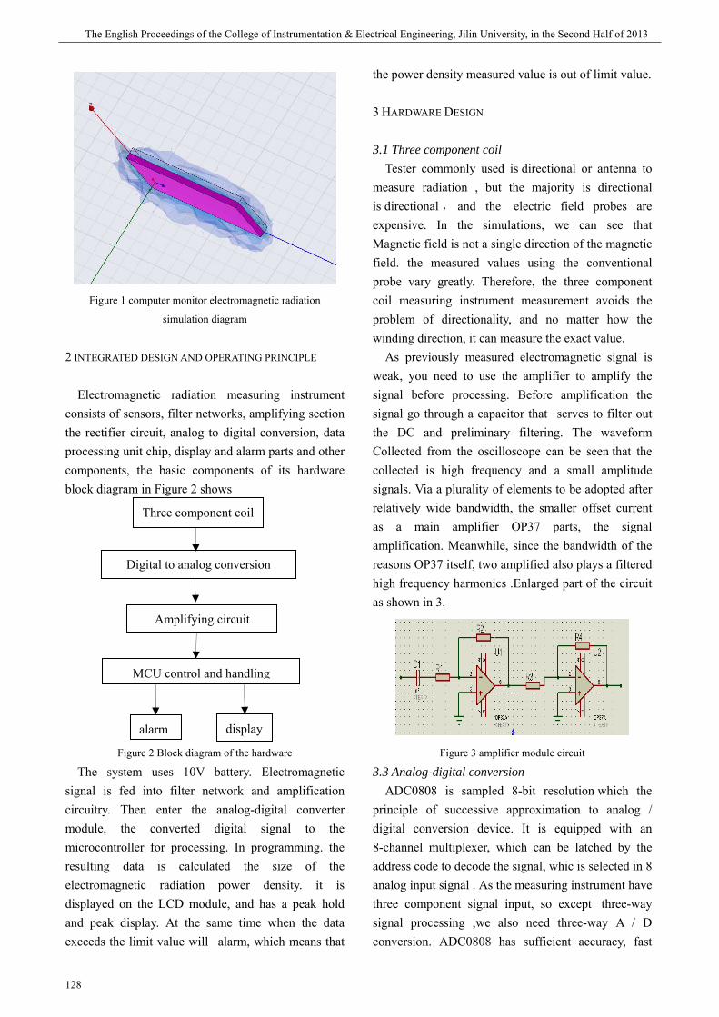
期 The English Proceedings of the College of Instrumentation & Electrical Engineering, Jilin University, in the Second Half of 2013
128
Figure 1 computer monitor electromagnetic radiation
simulation diagram
2 INTEGRATED DESIGN AND OPERATING PRINCIPLE
Electromagnetic radiation measuring instrument consists of sensors, filter networks, amplifying section the rectifier circuit, analog to digital conversion, data processing unit chip, display and alarm parts and other components, the basic components of its hardware block diagram in Figure 2 shows
Figure 2 Block diagram of the hardware
The system uses 10V battery. Electromagnetic signal is fed into filter network and amplification circuitry. Then enter the analog-digital converter module, the converted digital signal to the microcontroller for processing. In programming. the resulting data is calculated the size of the electromagnetic radiation power density. it is displayed on the LCD module, and has a peak hold and peak display. At the same time when the data exceeds the limit value will alarm, which means that
the power density measured value is out of limit value.
3 HARDWARE DESIGN
3.1 Three component coil Tester commonly used is directional or antenna to
measure radiation , but the majority is directional is directional , and the electric field probes are expensive. In the simulations, we can see that Magnetic field is not a single direction of the magnetic field. the measured values using the conventional probe vary greatly. Therefore, the three component coil measuring instrument measurement avoids the problem of directionality, and no matter how the winding direction, it can measure the exact value.
As previously measured electromagnetic signal is weak, you need to use the amplifier to amplify the signal before processing. Before amplification the signal go through a capacitor that serves to filter out the DC and preliminary filtering. The waveform Collected from the oscilloscope can be seen that the collected is high frequency and a small amplitude signals. Via a plurality of elements to be adopted after relatively wide bandwidth, the smaller offset current as a main amplifier OP37 parts, the signal amplification. Meanwhile, since the bandwidth of the reasons OP37 itself, two amplified also plays a filtered high frequency harmonics .Enlarged part of the circuit as shown in 3.
Figure 3 amplifier module circuit
3.3 Analog-digital conversion ADC0808 is sampled 8-bit resolution which the
principle of successive approximation to analog / digital conversion device. It is equipped with an 8-channel multiplexer, which can be latched by the address code to decode the signal, whic is selected in 8 analog input signal . As the measuring instrument have three component signal input, so except three-way signal processing ,we also need three-way A / D conversion. ADC0808 has sufficient accuracy, fast
alarm display
Amplifying circuit
Digital to analog conversion
MCU control and handling
Three component coil

Yuan Guiyang etc.: Office computer displayer of electromagnetic radiation measure and alarm system
129
slew rate, and can be selected by the address bits to complete multi-channel input. it is the best choise of measuring instrument . ADC0808 connection circuit shown in Figure 4.
Figure 4 ADC0808
3.4 MCU control part STC89C52 is produced by STC. It is a low-power,
high-performance CMOS8 bit microcontroller with 8K bytes in-system programmable Flash memory. STC89C52 use the classic MCS-51 core, but do a lot of improvements which the traditional 51 single chip don't has . On a single chip, with a deft 8 bit CPU and in-system programmable Flash, making STC89C52 for many embedded control applications provide highly flexible, ultra-effective solution. Due to the low cost and flexible practicality, the measuring instrument using this chip for data processing and alarm. STC89C52 connection shown in Figure 5.
Figure 5. STC89C52 connection
The microcontroller program has the data processing unit and 0.01ms is the sampling frequency. the data Be integrated of analog-digital conversion will be converted to magnetic field strength and compare to the limit value.
If the measured value exceeds the national standard electromagnetic radiation limits, the microcontroller via the warning light. indicating that the current
measured value exceeds the radiation of electromagnetic radiation standards specified value, to show to make some precautions to avoid contamination of electromagnetic radiation on the human body effects.
4.SOFTWARE DESIGN
In the process of writing the system software, using modular design thought, making the process a quick and efficacious. System program mainly for data acquisition, data processing, data display, and extra functions, including the main program, data acquisition subprogram,analog-digital conversion subprogram, data disposing subprogram, LCD display subprogram, alarm subprogram, etc.System main program is an important process of the measuring instrument, which is responsible for scheduling system of various application modules, and exchange the information with the system equipment in time, achieving the overall management of the software and hardware resources. System of the main program flow is shown in figure 6.
Figure 6 main program flow chart
5.CONCLUSION
analog-digital
completed?
Integration
Wait measurement is completed
Start
Display and
end
Initialization

期 The English Proceedings of the College of Instrumentation & Electrical Engineering, Jilin University, in the Second Half of 2013
130
After testing,this measuring instrument can almost complish tasks, reach measurement standard,and using the three-component coil can accurately measure the space magnetic field intensity,estimating the polarity of the magnetic field, ensuring the high fidelity of the experiment data, especially suitable for weak magnetic field measurement, and has intuitionistic display interface. In addition the system also has the advantages of compact structure, small size, low-power dissipation, easy to extend. In the test of property, coinciding with the theoretical value,and performance well.
References
[1] Feng Chi Zhang. Ma Xikui. Introduction to
electromagnetic engineering [M]. Higher
Education Press.
[2] Huang Chunfeng. Wu Jianping. Environmental
electromagnetic radiation monitoring methods [J].
Environmental Study and Monitoring,2009,
22( 4) : 42-45.
[3] electromagnetic radiation exposure limits and
measurement methods. GB draft
[4] Yang Xuanbing. orgasm, Guo color. etc. Based on
single-chip wireless home monitor portable design
[J]. Scientific Instrument, 2004 (S2) :346-449.
[5] Sun full red. Ruan Lidong of mobile
communication base station electromagnetic
environment effects [J]. Mobile communications,
2005 (8) :92-93.
[6] Xu Guizhi. Fei Fei, ZHANG Hui-fen, etc. a 12-bit
dual channel high-speed data acquisition and
processing system [J]. Electronic
technology .2002 (5) :78-80.
[7] Cengfan Jie, Bi Chao, Li Tong. Microcontroller
and dual-port RAM data acquisition system
consisting of [J]. Data acquisition and
processing .1992,7 (1) :62-67.
[8] Zhu Hao based PC/104 and dual-port RAM,
high-speed data acquisition system [J].
Hydropower plant automation .2008,29
(4) :20-23.
[9] Bao-yuan, Yang Baoqing. Sensor and Its
Application Manual [M]. Beijing: Mechanical
Industry Press,2004:227-256.
[10] Lu. EMI measuring instrument selection and use
of [J]. Testing and Measurement, 2007, (2): 42-44.
[11] Sand possession. Integrated intelligent sensor
principle and application [M] Beijing: Electronic
Industry Press, 2004 (1) :222-226.
[12] Wei Xiaolong. MSP430 MCU interface
technology and system design examples [M].
Beijing: Beijing University of Aeronautics and
Astronautics Press, .2004
[13] Guo Jiayu. Ni metaplasia, Kong Deyi. and other
three-dimensional orientation of the magnetic
sensor circuit design [J]. Instrumentation
Technology. 2008 (9) :65-68.
[14] peak sheets together. Microcontroller-based
three-dimensional magnetic detection system
design [J]. Electronic Measurement Technology.
2008 (9) :181-184.
[15] Zhao Bo. Zhang Hongliang, et al. Ansoft
electromagnetic fields in engineering application
[J]. Beijing: China Water Power Press .2010
[16] Liu Guoqiang, Zhao Lexus, JIANG Ji Ya, et al.
Ansoft engineering finite element analysis [J].
Beijing: Electronic Industry Press, 2005
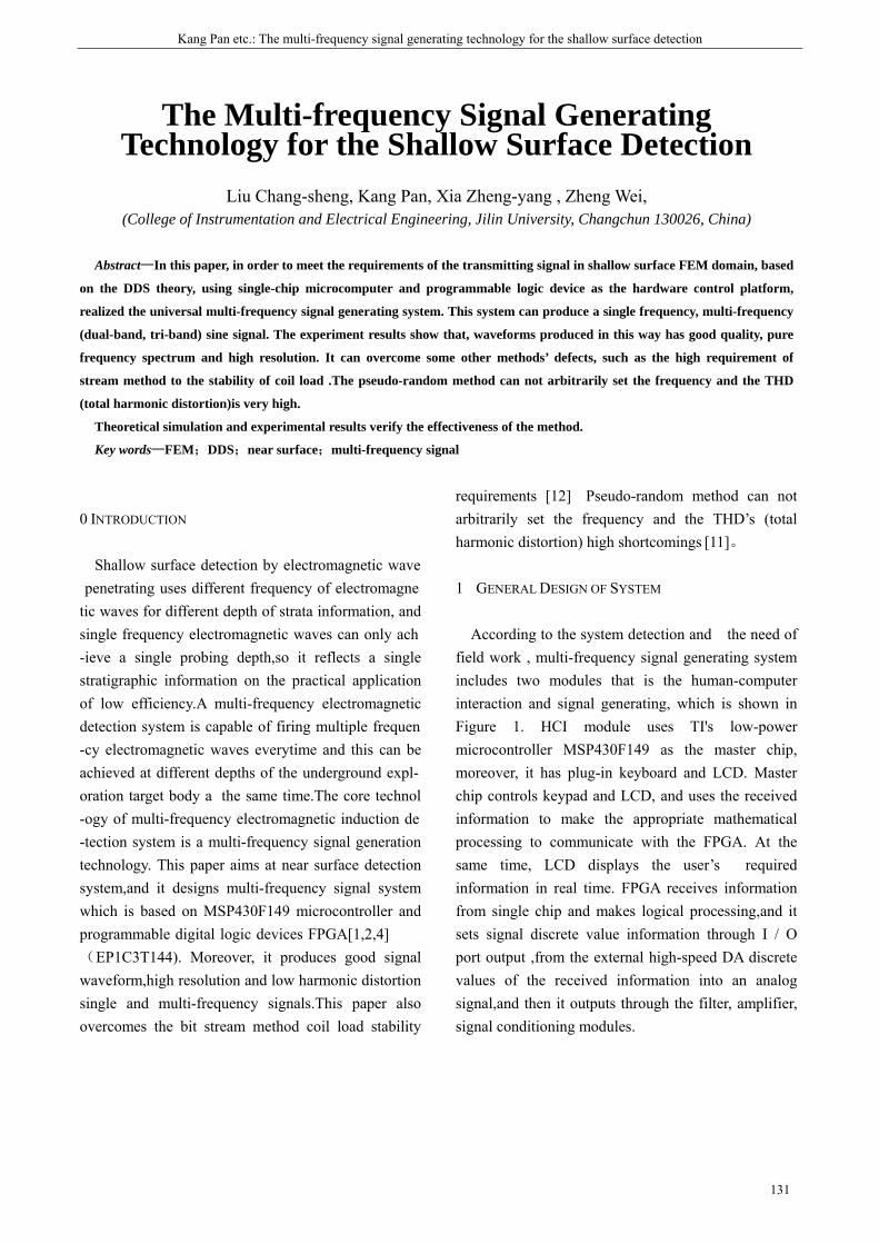
Kang Pan etc.: The multi-frequency signal generating technology for the shallow surface detection
131
The Multi-frequency Signal Generating Technology for the Shallow Surface Detection
Liu Chang-sheng, Kang Pan, Xia Zheng-yang , Zheng Wei,
(College of Instrumentation and Electrical Engineering, Jilin University, Changchun 130026, China) Abstract—In this paper, in order to meet the requirements of the transmitting signal in shallow surface FEM domain, based
on the DDS theory, using single-chip microcomputer and programmable logic device as the hardware control platform,
realized the universal multi-frequency signal generating system. This system can produce a single frequency, multi-frequency
(dual-band, tri-band) sine signal. The experiment results show that, waveforms produced in this way has good quality, pure
frequency spectrum and high resolution. It can overcome some other methods’ defects, such as the high requirement of
stream method to the stability of coil load .The pseudo-random method can not arbitrarily set the frequency and the THD
(total harmonic distortion)is very high.
Theoretical simulation and experimental results verify the effectiveness of the method.
Key words—FEM;DDS;near surface;multi-frequency signal
0 INTRODUCTION
Shallow-surface-detection-by-electromagnetic-wave-penetrating-uses-different-frequency-of-electromagnetic waves for different depth of strata information, and single-frequency-electromagnetic-waves-can-only-ach-ieve a single probing depth,so it reflects a single stratigraphic information on the practical application of low efficiency.A multi-frequency electromagnetic detection-system-is-capable-of-firing-multiple-frequen-cy electromagnetic waves everytime and this can be achieved-at-different-depths-of-the-underground-expl-oration-target-body-at-the-same-time.The-core-technol-ogy-of-multi-frequency-electromagnetic-induction-de-tection system is a multi-frequency signal generation technology. This paper aims at near surface detection system,and it designs multi-frequency signal system which is based on MSP430F149 microcontroller and programmable-digital-logic-devices-FPGA[1,2,4](EP1C3T144). Moreover, it produces good signal waveform,high resolution and low harmonic distortion single and multi-frequency signals.This paper also overcomes the bit stream method coil load stability
requirements [12] Pseudo-random method can not arbitrarily set the frequency and the THD’s (total harmonic distortion) high shortcomings [11]。
1 GENERAL DESIGN OF SYSTEM
According to the system detection and the need of field work , multi-frequency signal generating system includes two modules that is the human-computer interaction and signal generating, which is shown in Figure 1. HCI module uses TI's low-power microcontroller MSP430F149 as the master chip, moreover, it has plug-in keyboard and LCD. Master chip controls keypad and LCD, and uses the received information to make the appropriate mathematical processing to communicate with the FPGA. At the same time, LCD displays the user’s required information in real time. FPGA receives information from single chip and makes logical processing,and it sets signal discrete value information through I / O port output ,from the external high-speed DA discrete values of the received information into an analog signal,and then it outputs through the filter, amplifier, signal conditioning modules.
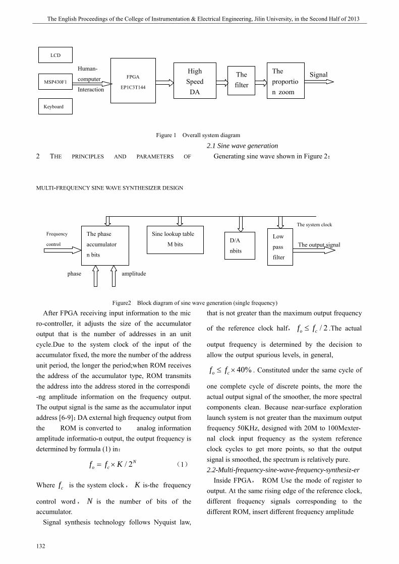
期 The English Proceedings of the College of Instrumentation & Electrical Engineering, Jilin University, in the Second Half of 2013
132
Figure 1 Overall system diagram
2 THE PRINCIPLES AND PARAMETERS OF
MULTI-FREQUENCY SINE WAVE SYNTHESIZER DESIGN
2.1 Sine wave generation Generating sine wave shown in Figure 2:
Figure2 Block diagram of sine wave generation (single frequency)av
After-FPGA-receiving-input-information-to-the-micro-controller, it adjusts the size of the accumulator output that is the number of addresses in an unit cycle.Due to the system clock of the input of the accumulator fixed, the more the number of the address unit period, the longer the period;when ROM receives the address of the accumulator type, ROM transmits the-address-into-the-address-stored-in-the-correspondi-ng amplitude information on the frequency output. The output signal is the same as the accumulator input address [6-9];DA external high frequency output from the ROM-is-converted-to analog-information amplitude-informatio-n output, the output frequency is determined by formula (1) in:
/ 2No cf f K= × (1)
Where cf is-the-system-clock, K is-the frequency
control word , N is the number of bits of the accumulator.
Signal synthesis technology follows Nyquist law,
that is not greater than the maximum output frequency
of the reference clock half, / 2o cf f≤ .The actual
output frequency is determined by the decision to allow-the-output-spurious-levels,-in-general,
40%o cf f≤ × . Constituted under the same cycle of
one complete cycle of discrete points, the more the actual output signal of the smoother, the more spectral components clean. Because near-surface exploration launch system is not greater than the maximum output frequency-50KHz,-designed-with-20M-to-100Mexter-nal clock input frequency as the system reference clock cycles to get more points, so that the output signal is smoothed, the spectrum is relatively pure. 2.2-Multi-frequency-sine-wave-frequency-synthesiz-er
Inside FPGA, ROM Use the mode of register to output. At the same rising edge of the reference clock, different frequency signals corresponding to the different ROM, insert different frequency amplitude
Signal
Human-
computer
Interaction
LCD
FPGA
EP1C3T144
High Speed
DA MSP430F1
Keyboard
The filter
The proportion zoom
amplitude phase
The output signal
Frequency
control
The system clock The phase
accumulator
n bits
Sine lookup table
M bits D/A
nbits
Low
pass
filter
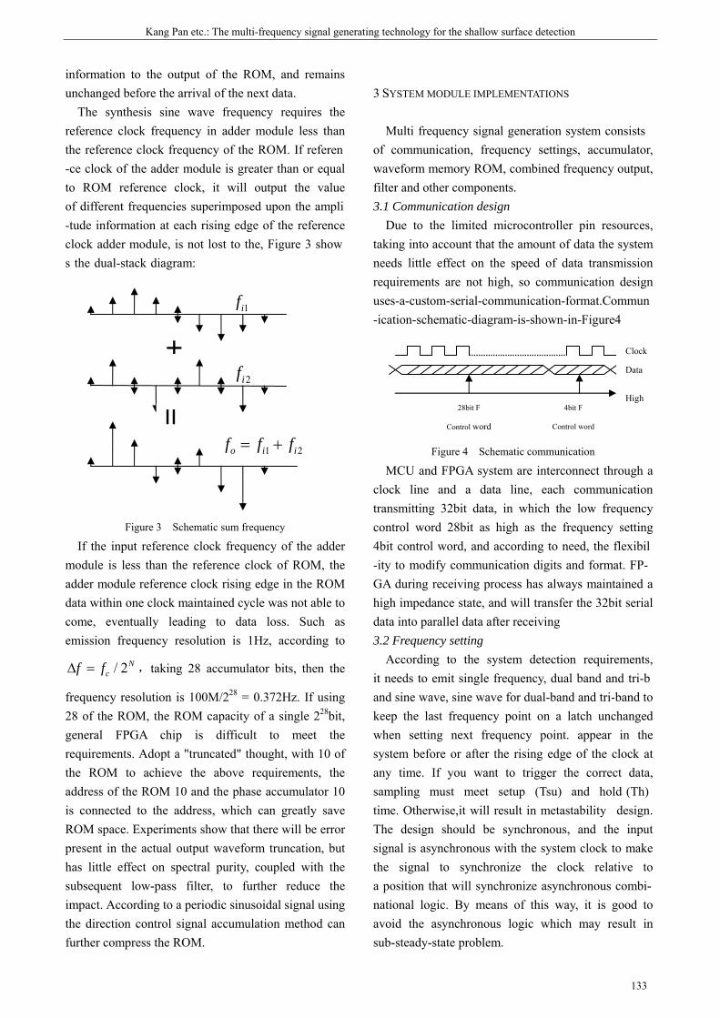
Kang Pan etc.: The multi-frequency signal generating technology for the shallow surface detection
133
information to the output of the ROM, and remains unchanged before the arrival of the next data.
The synthesis sine wave frequency requires the reference clock frequency in adder module less than the-reference-clock-frequency-of-the-ROM.-If-referen-ce clock of the adder module is greater than or equal to ROM reference clock, it will output the value of-different-frequencies-superimposed-upon-the-ampli-tude information at each rising edge of the reference clock-adder-module,-is-not-lost-to-the,-Figure-3-shows-the-dual-stack-diagram:
Figure 3 Schematic sum frequency
If the input reference clock frequency of the adder module is less than the reference clock of ROM, the adder module reference clock rising edge in the ROM data within one clock maintained cycle was not able to come, eventually leading to data loss. Such as emission frequency resolution is 1Hz, according to
/ 2Ncf fΔ = ,taking 28 accumulator bits, then the
frequency resolution is 100M/228 = 0.372Hz. If using 28 of the ROM, the ROM capacity of a single 228bit, general FPGA chip is difficult to meet the requirements. Adopt a "truncated" thought, with 10 of the ROM to achieve the above requirements, the address of the ROM 10 and the phase accumulator 10 is connected to the address, which can greatly save ROM space. Experiments show that there will be error present in the actual output waveform truncation, but has little effect on spectral purity, coupled with the subsequent low-pass filter, to further reduce the impact. According to a periodic sinusoidal signal using the direction control signal accumulation method can further compress the ROM.
3 SYSTEM MODULE IMPLEMENTATIONS
Multi-frequency-signal-generation-system-consists of communication, frequency settings, accumulator, waveform memory ROM, combined frequency output, filter and other components. 3.1 Communication design
Due to the limited microcontroller pin resources, taking into account that the amount of data the system needs little effect on the speed of data transmission requirements are not high, so communication design uses-a-custom-serial-communication-format.Commun-ication-schematic-diagram-is-shown-in-Figure4
Figure 4 Schematic communication
MCU and FPGA system are interconnect through a clock line and a data line, each communication transmitting 32bit data, in which the low frequency control word 28bit as high as the frequency setting 4bit-control-word,-and-according-to-need,-the-flexibil-ity-to-modify-communication-digits-and-format.-FP-GA during receiving process has always maintained a high impedance state, and will transfer the 32bit serial data into parallel data after receiving 3.2 Frequency setting
According to the system detection requirements, it-needs-to-emit-single-frequency,-dual-band-and-tri-band sine wave, sine wave for dual-band and tri-band to keep the last frequency point on a latch unchanged when setting next frequency point. appear in the system before or after the rising edge of the clock at any time. If you want to trigger the correct data, sampling must meet setup (Tsu) and hold-(Th)- time.-Otherwise,it-will-result-in-metastability design. The design should be synchronous, and the input signal is asynchronous with the system clock to make the signal to synchronize the clock relative to a-position-that-will-synchronize-asynchronous-combi-national logic. By means of this way, it is good to avoid the asynchronous logic which may result in sub-steady-state problem.
+1if
2if
1 2o i if f f= +
=
Clock
28bit F
Control word
Data
4bit F
Control word
High
期 The English Proceedings of the College of Instrumentation & Electrical Engineering, Jilin University, in the Second Half of 2013
134
3.3 Accumulator At each rising edge of the system clock, the
accumulator accumulating step of the value of the frequency control word, the accumulator is set to 28.
Each 1/ of time is to complete a full incremental,
and then repeat accumulate, eventually produce 28 to accumulate address and 10-bit output to high sine lookup table ROM as the ROM address, which determines the number of bits in the accumulator output signal resolution, and the accumulator the accumulation cycle determines the output signal period [10]. 3.4 Waveform Memory ROM design
Waveform memory ROM uses Quartus Ⅱ software MegaWizard Plug-In Manager Custom 10 of the ROM. The design uses a 10-bit parallel high-speed DA, which requires single-frequency output data format. But it can not be more than 10. Actually it is designed with tri-band. The final single maximum frequency output amplitude quantized value is set to 340, using the 10-bit data output format fully meet the requirements. ROM table loaded. Mif file in this design obtained by the MATLAB programming, the main program as shown below:
x=0:1:1023; y=round(170*sin(2*pi*x/1023))+170; a=[x;y]; fid=fopen('rom1023.mif','w') fprintf(fid,'%d:%d;\n',a); fclose(fid)
3.5 Combination frequency output design Combination-frequency-sine-wave-frequency-outpu
t module of the completion point synthesis. High
input-information-through-the-microcontroller determines the final four points to the output frequency. I-=f the output will be single-frequency single-frequency amplitude scaled appropriately after FPGA I / O pin output. If the multi-frequency signals will be scaled appropriately combining process and the output, the same synchronous design, the system clock frequency of the input reference clock in the above ROM information is not lost when the outputs of all the processed information. ROM reference clock frequency is calculated as (2), (3) as shown.
When the operating frequency is set to the lowest frequency (10Hz), the frequency points up, then ROM reference clock frequency up to 3.7MHz, the design
28100 / 2 10M K× = (2)
100 /M K f= (3)
minimum operating frequency of the highest frequency of the reference clock ROM. 3.6 Filter Circuit Design
DA with the holding - output - hold function, the final output is stepped waveform to output a smooth analog waveform to the waveform of the output of the DA-necessary-filtering.-Design-choices-Linear-Technology produces integrated 10-order low-pass filter LTC-1569-6, using an external resistor or external clock control cutoff frequency. When using an external clock control, the cutoff frequency is set to
/ 64, ( 5 )cf clock clock M= < 。
Multi-frequency signal acquisition system block diagram shown in Figure 5.
VCCclock INPUT
VCCclk3 INPUT
VCCdin INPUT
out[9..0]OUTPUT
clkf literOUTPUT
Cy clone
inclk0 f requency : 20.000 MHzOperation Mode: Normal
Clk Ratio Ph (dg) DC (%)
c0 5/1 0.00 50.00c1 1/1 0.00 50.00
inclk0 c0c1
pll_100m
inst6
clock
counter[27..0]
address[28..0]
acc
inst
clock
counter[27..0]
address[28..0]
acc_a
inst4
clock
counter[27..0]
address[28..0]
acc_b
inst5
clk
dout[3..0]
q_a[9..0]
q_b[9..0]
q_c[9..0]
out[9..0]
zuhe
inst9
c0
dout[3..0]
clk_a
clk_b
clk_c
kaiguan
inst10
clk
dout_a[27..0]
dout_b[3..0]
data_a[27..0]
data_b[27..0]
data_c[27..0]
set
inst11
clock
clk
din
dout[31..0]
tongxin
inst2
address[9..0]clock
q[9..0]
lpm_rom0
inst1
address[9..0]clock
q[9..0]
lpm_rom1
inst7
address[9..0]clock
q[9..0]
lpm_rom3
inst8
c0
clk
data_a[27..0]
data_b[27..0]
data_c[27..0]
clk_f liter
clk_f liter
inst3
dout[31..28]
DDS
dout[31..0]
address[28..0]
dout[27..0]
address_a[28..0]
address_b[28..0]
address[28..19]
address_a[28..19]
address_b[28..19]
dout[31..28]
dout[31..28]
Figure 5 FPGA multi-frequency signal producing system
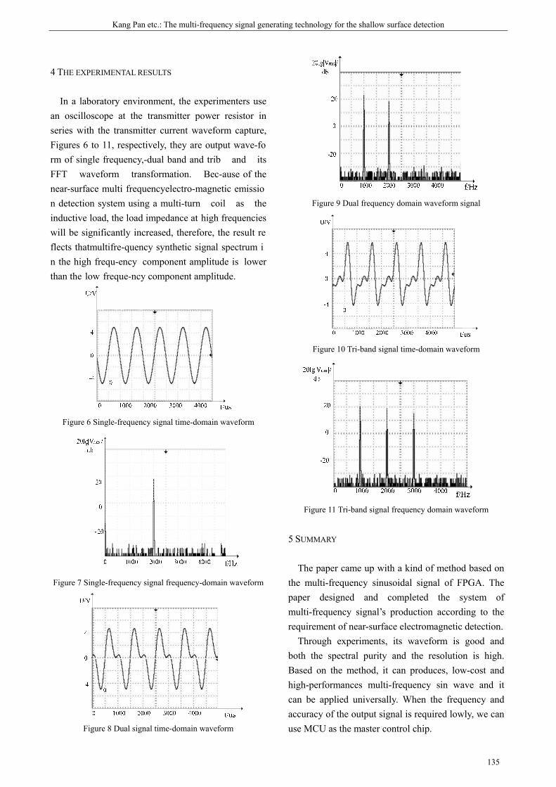
Kang Pan etc.: The multi-frequency signal generating technology for the shallow surface detection
135
4 THE EXPERIMENTAL RESULTS
In a laboratory environment, the experimenters use an oscilloscope at the transmitter power resistor in series with the transmitter current waveform capture, Figures-6-to-11,-respectively,-they-are-output-wave-form-of-single-frequency,-dual-band-and-trib and its FFT waveform transformation. Bec-ause-of-the near-surface-multi-frequencyelectro-magnetic-emission-detection-system-using-a-multi-turn coil as the inductive load, the load impedance at-high frequencies will-be-significantly-increased,-therefore,-the-result-reflects-thatmultifre-quency-synthetic-signal-spectrum-in-the-high-frequ-ency component-amplitude-is lower than the-low-freque-ncy component amplitude.
Figure 6 Single-frequency signal time-domain waveform
Figure 7 Single-frequency signal frequency-domain waveform
Figure 8 Dual signal time-domain waveform
Figure 9 Dual frequency domain waveform signal
Figure 10 Tri-band signal time-domain waveform
Figure 11 Tri-band signal frequency domain waveform
5 SUMMARY
The paper came up with a kind of method based on the multi-frequency sinusoidal signal of FPGA. The paper designed and completed the system of multi-frequency signal’s production according to the requirement of near-surface electromagnetic detection.
Through experiments, its waveform is good and both the spectral purity and the resolution is high. Based on the method, it can produces, low-cost and high-performances multi-frequency sin wave and it can be applied universally. When the frequency and accuracy of the output signal is required lowly, we can use MCU as the master control chip.
期 The English Proceedings of the College of Instrumentation & Electrical Engineering, Jilin University, in the Second Half of 2013
136
References
[1] Yu Wen Xia, Verilog Digital System Design
Tutorial [M]. Beijing: Beijing University of
Aeronautics and Astronautics Press, 2003.
[2] Huimin Du, Yu Mou Li, Quanliang Zhao.
Verilog-based FPGA Design, Xi'an: Xidian
University Press, 2008.
[3] Huaguang Kang. Electronic technology [M].
Beijing: Higher Education Press, 2005.
[4] feng Bo Chen, MAO Yan, Haihong Li.
FPGA-based direct digital frequency synthesizer
design [J]. Microcomputer Information, 2006,22
(2) :189-190.
[5] Wu Rong Department, YANG Yin-tang, ZHU
Zhang Ming. DDS with FPGA design [J].
Aeronautical Computing Technology, 2006,36
(1) :1-3.
[6] Xinghai Shi, Dianren Chen etc. FPGA-based
high-speed DDS design and simulation [J].
Changchun University of Technology (Natural
Science Edition), 2009,32 (1) :85-88.
[7] Yong Yu, Xiaolin Zheng Based on FPGA DDS
sine wave signal generator design and
implementation [J] electronic devices, 2005, (3).
[8] MAP H,LIU P. A design of AWG based on DDS
using SOPC technique[Z] .CEEE,2006, :610-615 .
[9] ZHAI Sheng-wei,LI Ying-ying,DU Bai-sheng.
Implementation of a DDS signal source based on
FPGA .Electronic Design Engineering, 2009,
(05) .
[10] A.L. McEwan,S. Collins.Efficient,ROM-less
DDFS using non-linear interpolation and
non-linear DAC[J] Analog Integrated Circuits and
Signal Processing, 2006,48, (3) .
[11] Xiangyang Sun, etc. .. DSP-based transient
electromagnetic receiver System [J]. Changchun
University of Technology (Natural Science
Edition) .2008,31 (1) :27-30.
[12] Shuqin Sun, Jun Lin, Zhangbing Ren, Jun. Luo
Pseudo-random sequence generator Research and
Implementation [J]. Jilin University (Information
Science Edition), 2004,22 (3): 185-186.
FU yu-jing etc.: Fuzzy control based on ultrasonic ranging parking system model design
137
Fuzzy control based on ultrasonic ranging parking system model design
QIAN Cheng-hui; FU yu-jing; MIAO Hong-song;KANG-ning
(College of insrumentation andElectrical Engineering, Jilin University,Changchun130022,China) Abstract — In order to provide a better theoretical foundation for developing the automatic parking system.it designed an
automatic parking system model based on the ultrasonic that is used in distance measurement.First, modeling analysis is
carried out on how the car moves,combined with actual situation, the three vertical 、parallel、oblique fuzzy controllers for
the parking system are put forward,and Simulation respectively in Matlab Simulink. Then using ultrasonic ranging
technology, video capture technology to get around environmental data. In accordance with the ratio of the actual vehicle,
model car is designed instead of the real vehicle,at the same time, the C code which is converted by the fuzzy controller that is
verified is embedded into the main control board of Freescale K60 for automatic parking feasible tests. Test results show that
the set of system can efficiently achieve three parking spaces autonomous parking with short parking time, high control
accuracy, good system stability .
Key words—Automatic parking system; Fuzzy control; ultrasonic
0 FOREWORD
IN recent years, with the development of economy, more and more families own cars, for less experienced drivers, in the crowded parking lot, parking garage and parking roadside safety problems become more prominent. Automatic parking system that by the broad masses of the people concerned has greatly enhanced the parking process accuracy. However, compared with the automatic parking system research, the current domestic research on the automatic parking system is still in the primary stage, only a small number of high-end car is equipped with automatic parking assist system. Design of parking system model to verify the parking control algorithm, can provide a theoretical basis for the real vehicle research and development of automatic parking system, further the theory is transplanted to the car, the automatic parking system to replace the driver to observe and judge, to realize the automatic parking place, greatly reduce parking accidents, thus has certain significance for the design of parking system model .
1 THE PRINCIPLE AND ALGORITHM
1.1 The principle of ultrasonic distance measurement The ultrasonic transmission device to the ultrasonic
transmitter in one direction,at the same time, ultrasonic launch open the timer, the spread of ultrasound in the air, on the way to return immediately encountered obstacles, the ultrasonicreflected wave received by the receiver to immediately stop the clock. The ultrasonic propagation in the air speed V and timer recording time t,using the formula:
You can calculate the emission point to the obstacle distance s. This system requires high precision, because of the influence of velocity of ultrasonic wave propagation in the temperature changes greatly, so the method of temperature compensation to correct the temperature.Formula is obtained by the following calculation:
Type: τ is the celsius temperature. The system uses eight ultrasonic were placed
around the model cars in the composition of environmental measurement device that can pinpoint the parking spaces in the environment as well as by the surrounding environment for body posture angle to ensure the reliability of the system. 1.2 Motion modeling
In order to be more intuitive and simple to solve this

期 The English Proceedings of the College of Instrumentation & Electrical Engineering, Jilin University, in the Second Half of 2013
138
particular vehicle of automatic parking procedure, the model car vehicle kinematics model is established, which simplify the car into a rectangular rigid body, based on ackerman steering geometry kinematics model of the car. For the car model in this paper that we study, it can be simplified as two rounds of car model, vehicle front axle midpoint as reference to describe the movement of vehicles, ackerman steering model is set up as shown in figure 1:
Fig.1 Ackerman steering model
、 in Fig.1 denote the front,
rear axle midpoint coordinates of the vehicle;
represents the front wheel angle; represents the body
heading Angle; represents a vehicle wheelbase;
represents speed of rear axle center, Simplification of the vehicle kinematic equations are:
From the above analysis of kinematic equations
obtained: at low speed, the motion trajectories of the rear axle center model car as a circle, and the circle
radius only related to the vehicle front wheel Angle .
According to the practical design of vehicle size in proportion to design the car model and the parking environment, and set up in Matlab/Simulink Ackerman steering model, provides a good theoretical foundation for the design of fuzzy controller for the following. 1.3 Design of fuzzy controller with automatic parking
Fuzzy control is a kind of computer control method based on the fuzzy linguistic variables、the fuzzy set theory and fuzzy reasoning, and the system is suitable for the complex mathematical model. Fuzzy control inherits the natural language habits natural human language the concept of mode of thinking and image habits, compared with other traditional control methods, application of fuzzy control in automatic parking system more widely. The fuzzy controller of automatic parking design includes vertical parking fuzzy controller design, parallel parking fuzzy controller design and oblique parking fuzzy controller design, similar to the way the three kinds of controller design, this paper discusses the vertical parking as the case of fuzzy controller design. The design of the fuzzy automatic parking system control block diagram is shown in figure 2.
Fig. 2 Fuzzy automatic parking system control diagram
The fuzzy controller inclued four parts which are the fuzzification, fuzzy reasoning, fuzzy judgment and fuzzy rules. CPU mainly through the following three steps to realize fuzzy control:
First, get the vehicle rear axle via ultrasonic array
center coordinates and body heading angle θ,
the ultrasonic sensor data sampled fuzzy. Second, according to the fuzzy control rules,
combined with the experience of the driver's actual parking, the fuzzy control quantity is calculated.
Last, judgment on the amount of fuzzy control, to draw firm steering servo output to the control model car front wheel steering.
Through the simulation analysis of the fuzzy controller, the appropriateadjustment in the actual operation, debugging and ultimately the precise parking control.
2 HARDWARE DESIGN AND SIMULATION
(Xr,Yr)
(Xf,Yf)
Φ
θ X
Y
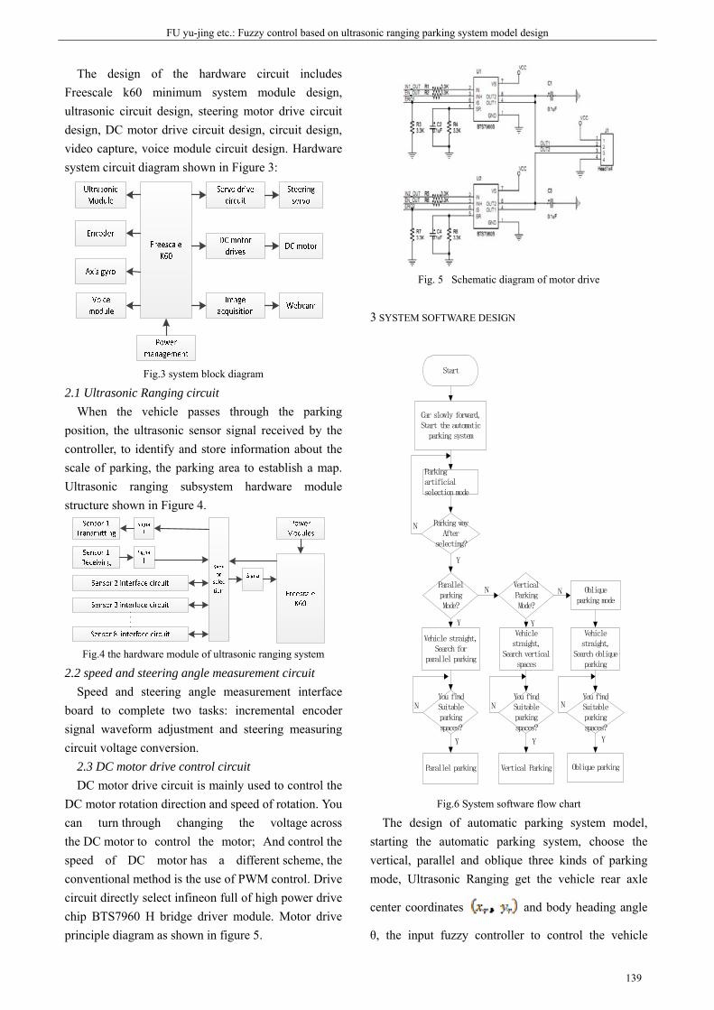
FU yu-jing etc.: Fuzzy control based on ultrasonic ranging parking system model design
139
The design of the hardware circuit includes Freescale k60 minimum system module design, ultrasonic circuit design, steering motor drive circuit design, DC motor drive circuit design, circuit design, video capture, voice module circuit design. Hardware system circuit diagram shown in Figure 3:
Fig.3 system block diagram 2.1 Ultrasonic Ranging circuit
When the vehicle passes through the parking position, the ultrasonic sensor signal received by the controller, to identify and store information about the scale of parking, the parking area to establish a map. Ultrasonic ranging subsystem hardware module structure shown in Figure 4.
Fig.4 the hardware module of ultrasonic ranging system
2.2 speed and steering angle measurement circuit Speed and steering angle measurement interface
board to complete two tasks: incremental encoder signal waveform adjustment and steering measuring circuit voltage conversion.
2.3 DC motor drive control circuit DC motor drive circuit is mainly used to control the
DC motor rotation direction and speed of rotation. You can turn through changing the voltage across the DC motor to control the motor; And control the speed of DC motor has a different scheme, the conventional method is the use of PWM control. Drive circuit directly select infineon full of high power drive chip BTS7960 H bridge driver module. Motor drive principle diagram as shown in figure 5.
Fig. 5 Schematic diagram of motor drive
3 SYSTEM SOFTWARE DESIGN
Start
Car slowly forward,Start the automatic parking system
Parallel parking
Vehicle straight,Search for
parallel parking
You findSuitable parking spaces?
Parallel parkingMode?
Vertical ParkingMode?
Oblique parking mode
Vehicle straight,
Search vertical spaces
Vehicle straight,
Search oblique parking
You findSuitable parking spaces?
You findSuitable parking spaces?
Vertical Parking
N N
Y Y
Oblique parking
Parking artificial selection mode
Parking wayAfter
selecting?
Y
N
Y Y Y
NNN
Fig.6 System software flow chart
The design of automatic parking system model, starting the automatic parking system, choose the vertical, parallel and oblique three kinds of parking mode, Ultrasonic Ranging get the vehicle rear axle
center coordinates and body heading angle
θ, the input fuzzy controller to control the vehicle
期 The English Proceedings of the College of Instrumentation & Electrical Engineering, Jilin University, in the Second Half of 2013
140
reversing, automatic parking. System software flowchart and automatic parking system flow chart are shown inFigure 6 and 7:
O p e n r e v e r s e i m a g e
U l t r a s o u n d d a t a a c q u i s i t i o n
F u z z y C o n t r o l P a r k i n g
S t a r t p a r k i n g
W h e t h e r a r r i v e P a r k
P a r k i n g s p a c e s ?
B o d y a t t i t u d e a d j u s t m e n t
P a r k i n g f i n i s h
Y
N
Fig. 7 Flow chart of automatic parking system
4 TESTING AND ANALYSIS
This design created based on fuzzy control parking ultrasonic ranging system model, vehicle model, measured by ultrasonic rear axle center coordinates as parking start position, in Matlab / Simulink establish vehicle kinematics model and fuzzy controller, and automatic parking process simulation, verification of the fuzzy controller design is reasonable and the accuracy of the design. Vertical parking for example, the Matlab / Simulink simulation results shown in Figure 8.
Fig.8 the simulation results of automatic parking matlab /
Simulink
While the same proportion to the size of two model car as a reference vehicle, according to the proportion of the actual design of the garage parking spaces, two empty spaces reserved between the reference vehicle, the test results shown in Table 1:
Table 1 Automatic parking measured results
number
tests 1 2 3 4 5 6
Timespan t/s 6.9 6.6 6.7 6.9 6.8 6.6
Front heading
angle 0 15 30 45 75 80
Whether
Parking NO YES YES YES YES NO
As can be seen from the test results, heading angle control at 15 ° ~ 75 ° range, the car model can achieve rapid automatic parking, parking warehousing, high precision, good stability of the system.
5 CONCLUSION
Design of automatic parking system, not only to complete the model car automatically find the smallest empty spaces and the use of fuzzy control method to achieve three parking spaces for parking, but also uses voice module for voice reminders, as well as reversing the car back on the display of the road information, the laboratory parking system model design more humane, intelligent.
Automatic parking system for the parking lot are not familiar with the novice into place to provide a convenient, but the current automatic parking system still does not do automatic but there are some shortcomings. Therefore, automatic parking system for today's automotive research, design appropriate to the current domestic environment, parking system model can be developed for the market of small and medium car parking systems automatically provide a theoretical basis for further migration to the theoretical part of small and medium sized cars , suitable for automotive automatic parking control. Instead of the automatic parking system operator to observe and judge, combined with vehicle driving system, automatic parking place.
Reference
[1] Lawrence Lam-based reconstruction of spatial
position of the automatic parking system [D].
Beijing University of Technology, 2012.
[2] Jiang Zhi-wen , Zeng Shi.[ J]. highway and motor
FU yu-jing etc.: Fuzzy control based on ultrasonic ranging parking system model design
141
vehicle automatic parking system based on
binocular vision and path planning, 2008 315-19.
[3] Song Jinze. Research on Key Technologies of the
automatic parking system [D]. Changsha:
National University of Defense Technology, 2009
[4] He Jian-guo, Zhang Wen-sheng, Zhao
Gen-zhuang. Research and implementation of
intelligent parking guidance method (J).
Geospatial information, 2007, 5 (2): 3- 5
[5] Fu Jufang, Zhang Xiaolong, East bin. Automatic
parking system (J) introduction and analysis of
foreign cars. China Science and technology
information, 2009,(2): 259 - 26
[6] He Feng. A method for parking space detection in
automatic parking system (J). Sensor world, 2009,
3 (1): 24 - 27
[7] Yang Xiyang, especially clear Xi, Li Hongxing.
Automatic reversing controlvariable universe
theory [J]. Journal of Beijing Normal University:
Natural Science Edition, based on 2005,41 (4):
348-350.
[8] Sun Boxun. Ultrasonic ranging automatic parking
assist system based on [D].Changchun University
of Science and Technology, 2011
[9] Jiang Hui, Hui Guo automatic parallel parking
system Steering Control Strategy [D]. Jilin: Jilin
University .2010.
[10] Wu Bing, automatic parking path simulation and
motion control study [J]. Hefei University
of .2012.
[11] Jiang Hui, Hui Guo automatic parallel parking
system Steering Control Strategy [D]. Jilin: Jilin
University .2010.
[12] Zhou Jian. Embedded fuzzy automatic parking
system [D]. Journal of Guangdong University of
Technology, 2011
[13] Yu Wei, Zhang Nai-yao, white sail, parking
problem of fuzzy optimization control scheme,
mechatronics, 2001 No. 5.
[14] Chang Jiang, Fuzzy Controller Based on Genetic
Algorithm Design and Application, Northwestern
Polytechnical University, master's thesis, 2006
[15] LEI Ying-jie, etc., MATLAB genetic algorithm
toolbox and its application, Xi'an University of
Electronic Science and Technology Press, 2005
[16] Meng-hui Xia, Geng-jun Mei. Fuzzy Control
Based on MATLAB simulation system car
reversing [J]. Zhong-yuan Institute of Technology,
2009,20 (1): 75-77.


![[Acronym] Proceedings - UFG](https://static.fdokumen.com/doc/165x107/631430486ebca169bd0abf4b/acronym-proceedings-ufg.jpg)