Langmuir monolayer approaches to protein recognition through molecular imprinting

IEEE
Proo
f
Electronic Transport in MolecularSelf-Assembled Monolayer Devices
WENYONG WANG, TAKHEE LEE, AND MARK A. REED, SENIOR MEMBER, IEEE
Invited Paper
A review on the mechanisms and characterization methods ofelectronic transport through self-assembled monolayers (SAMs) ispresented. Using SAMs of alkanethiols in a nanometer-scale-devicestructure, tunneling is unambiguously demonstrated as the main in-trinsic conduction mechanism for defect-free large bandgap SAMs,exhibiting well-known temperature and length dependencies. In-elastic electron tunneling spectroscopy exhibits clear vibrationalmodes of the molecules in the device, presenting direct evidence ofthe presence of molecules in the device.
Keywords—Molecular electronics, spectroscopy, tunneling.
I. INTRODUCTION
The suggestion [1] and demonstration [2] of utilizingmolecules as the active region of electronic devices hasrecently generated considerable interest in both the basictransport physics and potential technological applicationsof “molecular electronics” [3], [4], [71]. However, somereports of molecular mechanisms in electronic devices [5],[6], [72], [73] have been shown to be premature and due to
Manuscript received April 12, 2005; revised April 20, 2005. This work
was supported in part by the [AU: Are these grants,contracts, project numbers, etc.? Pleaseindicate for all numbers]DARPA/ONR underN00014-01-1-0657, in part by the ARO under DAAD19-01-1-0592,in part by the AFOSR under F49620-01-1-0358, in part by the NSF
DMR-0095215, and in part by NASA NCC 2-1363.[AU: Pleasespell out acronyms as needed throughout]
W. Wang was with the Department of Physics, Yale University, NewHaven, CT 06520 USA. He is now with the Semiconductor ElectronicsDivision, National Institute of Standards and Technology, Gaithersburg,MD 20899-8120 USA.
T. Lee was with the Department of Electrical Engineering, Yale Univer-sity, New Haven, CT 06520 USA. He is now with the Department of Ma-terials Science and Engineering, Gwangju Institute of Science and Tech-nology, Gwangju, 500-712, Korea.
M. A. Reed is with the Departments of Electrical Engineering and Ap-plied Physics, Yale University, New Haven, CT 06520 USA (e-mail: [email protected]).
Digital Object Identifier 10.1109/JPROC.2005.853544
filamentary conduction, [7], [74] highlighting the fabricationsensitivity of molecular structures and the need to institutereliable controls and methods to validate true moleculartransport [8]. A related problem is the characterization ofmolecules in the active device structure, including theirconfiguration, bonding, and indeed even their very presence.Here we present results on well-understood molecular as-semblies, which exhibit an understood classical transportbehavior and which can be used as a control for eliminating(or understanding) fabrication variables. Utilizing tunnelingspectroscopic methods, we present the first unambiguousevidence of the presence of molecules in the junction andfurther confirm the charge transport mechanism obtained bystandard current–voltage characterizations.
A molecular system whose structure and configuration aresufficiently well characterized such that it can serve as a stan-dard is the alkanethiol CH CH SH self-assembledmonolayer (SAM) [9]. This system is useful as a control,since properly prepared SAMs form single van der Waalscrystals, [9], [10] and presents a simple classical metal–in-sulator–metal (MIM) tunnel junction when fabricated be-tween metallic contacts due to the large HOMO–LUMO gap(HOMO: highest occupied molecular orbital; LUMO: lowestunoccupied molecular orbital) of approximately 8 eV1 [11],[12], [75]–[77].
Various surface analytical tools have been utilized toinvestigate the surface and bulk properties of the alka-nethiol SAMs, such as X-ray photoelectron spectroscopy,[13] Fourier transform infrared spectroscopy (FTIR), [14]Raman spectroscopy, [15] scanning tunneling microscopy(STM) [10] etc. For example, studies have shown that thebonding of the thiolate group to the gold surface is strongwith a bonding energy of 1.7 eV [9]. STM topographyexaminations revealed that alkanethiols adopt the com-mensurate crystalline lattice characterized by a
1Although the HOMO–LUMO gap of alkyl chain type molecules has beenreported (see ref [12]), there is no experimental data on the HOMO–LUMOgap for the Au/alkanethiol SAM/Au system. Eight electronvolts is com-monly used as the HOMO–LUMO gap of alkanethiol.
0018-9219/$20.00 © 2005 IEEE
PROCEEDINGS OF THE IEEE, VOL. 93, NO. 10, OCTOBER 2005 1

IEEE
Proo
f
superlattice of a [10], [16]. FTIR investiga-tion showed that the orientation of the alkane thiol SAMs onAu(111) surfaces are tilted 30 from the surface normal[17].
Electronic transport through alkanethiol SAMs havealso been characterized by STM [18], [19], conductingatomic force microscopy [20]–[23], mercury-drop junctions[24]–[27], cross-wire junctions [28], and electrochemicalmethods [29]–[31]. These investigations are exclusivelyat ambient temperature—clearly useful—but insufficientfor an unambiguous claim that the transport mechanismis tunneling (of course expected, assuming that the Fermilevels of the contacts lie within the large HOMO–LUMOgap). However, in the absence of temperature-dependentcurrent–voltage ( ) characteristics, other conductionmechanisms (such as thermionic, hopping, or filamen-tary conduction) cannot be excluded complicate [AU:Please clarify]the analysis, and thus such a claim ispremature.
Utilizing a nanometer-scale-device structure that incorpo-rates alkanethiol SAMs, we demonstrate devices that allow
and structure-dependent measurements [32], [33]with results that can be compared with accepted theoreticalmodels of MIM tunneling. The use of this fabrication ap-proach is not special in any way (other than that we haveso far found it to be successful)—indeed we stress thatany successful device fabrication method should yield theresults described below if one is characterizing the intrinsicmolecular transport properties.
The electronic transport is further investigated withthe technique of inelastic electron tunneling spectroscopy(IETS) [33]. IETS was developed in the 1960s as a powerfulspectroscopic tool to study the vibrational spectrum oforganic molecules confined inside metal–oxide–metal junc-tions [34]–[38]. In our study, IETS is utilized for the purposeof molecule identification, chemical bonding, and conduc-tion mechanism investigations of the “control” SAMs. Theexclusive presence of well-known vibrational modes of thealkanes used are direct evidence of the molecules in the de-vice structure, something that has to date only been inferred(with good reason, but nonetheless not unambiguously). Thevibrational modes, exclusively identified as alkanes (as wellas contact modes) are difficult to interpret in any way otherthan as components in the active region of the device. Theinelastic tunneling spectra also demonstrate that electronictunneling occurs through the molecules, confirming the con-duction mechanism obtained by characterizations.The specific spectral lines also yield intrinsic linewidthsthat may give insight into molecular conformation, andmay prove to be a powerful tool in future molecular devicecharacterization.
II. EXPERIMENT
Electronic transport measurements on alkanethiol SAMswere performed using a device structure similar to one re-ported previously [32], [33], [39]–[41], [78]. In this device, anumber of molecules ( several thousands) are sandwiched
between two metallic contacts. This technique provides astable device structure and makes cryogenic measurementspossible. The device fabrication starts with a high resistivitysilicon wafer with low stress Si N film deposited on bothsides by low pressure chemical vapor deposition (LPCVD).By standard photolithography processing, a suspendedSi N membrane (size of m m and thickness of
70 nm) is fabricated on the topside of the wafer. Subse-quent e-beam lithography and reactive ion etching creates asingle pore with a diameter of tens of nanometers throughthe membrane. As the next step, 150 nm of gold is thermallyevaporated onto the topside of the wafer to fill the pore andform one of the metallic contacts.
The device is then transferred into a molecular solu-tion to deposit the SAM layer. For our experiments, a 5mM alkanethiol solution is prepared by adding Lalkanethiols into 10 mL ethanol.2 The deposition is donein solution for 24 h inside a nitrogen-filled glove boxwith an oxygen level of less than 100 ppm. Three alka-nemonothiol molecules of different molecular lengths-oc-tanethiol (CH CH SH; denoted as C8, for the numberof alkyl units), dodecanethiol (CH CH SH, denotedas C12), and hexadecanethiol (CH CH SH, denotedas C16) and one alkanedithiol molecule, octanedithiol(HS CH SH, denoted as C8-dithiol) were used to formthe active molecular components.3
In order to statistically determine the pore size, test pat-terns (arrays of pores) were created under similar fabricationconditions. This indirect measurement of device size is donebecasue scanning electron microscope (SEM) examinationof the actual device can cause hydrocarbon contamination ofthe device and subsequent contamination of the monolayer.From regression analysis of 298 pores, the device sizes of theC8, C12, C16, and C8-dithiol samples are determined as 50
8, 45 2, 45 2, and 51 5 nm in diameter, respec-tively. A more ideal (less parasitic) C8 sample supersedesthat of previous reports [32] and derived parameters from thetwo data sets agree to within a standard error. We will usethese device areas as the effective contact areas. Althoughone could postulate that the actual area of metal that contactsthe molecules may be different, there is little reason to pro-pose it would be different as a function of length over therange of alkanethiols used, and at most would be a constantsystematic error.
The sample is then transferred in ambient conditions to anevaporator that has a cooling stage to deposit the opposingAu contact. During the thermal evaporation (under the pres-sure of 10 torr), liquid nitrogen is kept flowing throughthe cooling stage in order to avoid thermal damage to themolecular layer [32], [42]. This technique reduces the kineticenergy of evaporated Au atoms at the surface of the mono-layer, thus preventing Au atoms from punching through themonolayer. For the same reason, the evaporation rate is keptvery low. For the first 10 nm of gold evaporated, the rate isless than 0.1 s. Then the rate is increased slowly to 0.5
2Ethanol and alkane molecules were purchased from Sigma-Aldrich.3Ethanol and alkane molecules were purchased from Sigma-Aldrich.
2 PROCEEDINGS OF THE IEEE, VOL. 93, NO. 10, OCTOBER 2005
IEEE
Proo
f
s for the rest of the evaporation and a total of 200 nm ofgold is deposited to form the contact.
The device is subsequently packaged and loaded into alow-temperature cryostat. The sample temperature is variedfrom 300 K to 4.2 K by flowing cryogen vapor onto thesample (and thermometer) using a closed loop tempera-ture controller. Two-terminal dc measurements areperformed using a semiconductor parameter analyzer. In-elastic electron tunneling spectra are obtained via a standardlock-in second harmonic measurement technique [34], [35].A synthesized function generator is used to provide boththe modulation and the lock-in reference signal. The secondharmonic signal (proportional to ) is directlymeasured using a lock-in amplifier, which is checked to beconsistent with a numerical derivative of the first harmonicsignal (proportional to ). Various modulation am-plitudes and frequencies are utilized to obtain the spectra.The ac modulation is added to a dc bias using operationalamplifier-based custom circuitry [43].
III. THEORY
Possible conduction mechanisms are elucidated by de-termining characteristic current, temperature and voltagedependencies [44] (we do not discuss filamentary tunnelingmechanisms, which are easier to categorize [45], [79],[80]). Based on whether thermal activation is involved, theconduction mechanisms fall into two distinct categories:1) thermionic or hopping conduction, which has tempera-ture-dependent behavior, and 2) direct tunneling orFowler–Nordheim tunneling which does not have tempera-ture-dependent behavior. For example, thermionic andhopping conductions have been observed for 4-thioacetyl-biphenyl SAMs [39] and 1,4-phenelyene diisocyanideSAMs [78]. On the other hand, the conduction mechanism isexpected to be tunneling when the Fermi levels of contactslie within the large HOMO–LUMO gap for short lengthmolecule, as for the case of alkanethiol molecular system4
[11], [12][75]–[77]. Previous work on Langmuir–Blodgettalkane monolayers [46], [81] exhibited a significant im-purity-dominated transport component, complicating theanalysis. measurements on self-assembled alkanethiolmonolayers have also been reported [18]–[28], [47]; how-ever, all of these measurements were performed at a fixedtemperature (300 K) which is insufficient to prove tunnelingas the dominant mechanism.
To describe the transport through a molecular systemhaving HOMO and LUMO energy levels, one of the ap-plicable models is the Franz two-band model [48]–[51],[82], [83]. This model provides a non-parabolic energy-mo-mentum dispersion relationship by considering the
4Although the HOMO–LUMO gap of alkyl chain type molecules has beenreported (see ref [12]), there is no experimental data on the HOMO–LUMOgap for the Au/alkanethiol SAM/Au system. Eight electronvolts is com-monly used as the HOMO–LUMO gap of alkanethiol.
contributions of both the HOMO and LUMO energy levels[48]
(1)
where is the imaginary part of wave vector of elec-trons, is the electron effective mass, isPlanck’s constant, is the electron energy, and is theHOMO–LUMO energy gap. From this nonparabolicrelationship, the effective mass of the electron tunnelingthrough the SAM can be deduced by knowing the barrierheight of the metal–SAM–metal junction.
When the Fermi level of the metal is aligned close enoughto one energy level (either HOMO or LUMO), the effect ofthe other distant energy level on the tunneling transport isnegligible, and the widely used Simmons model [52] is an ex-cellent approximation [53], [84]. Simmons model expressedthe tunneling current density through a barrier in the tun-neling regime of as [24], [52]
(2)
where is the electron mass, is the barrier width, isthe barrier height, and is the applied bias. For molecularsystems, the Simmons model has been modified with a pa-rameter [24], [32]. is a unitless adjustable parameter thatis introduced to provide either a way of applying the tun-neling model of a rectangular barrier to tunneling through anonrectangular barrier [24], or an adjustment to account forthe effective mass of the tunneling electrons through arectangular barrier [24], [32], [51], [54], or both. cor-responds to the case for a rectangular barrier and bare elec-tron mass. By fitting individual data using (2), and
values can be obtained.Equation (2) can be approximated in two limits: low bias
and high bias as compared with the barrier height . Forthe low-bias range, (2) can be approximated as [52]
(3a)
To determine the high-bias limit, we compare the relativemagnitudes of the first and second exponential terms in (2).
WANG et al.: ELECTRONIC TRANSPORT IN MOLECULAR SELF-ASSEMBLED MONOLAYER DEVICES 3

IEEE
Proo
f
At high bias, the first term is dominant and thus the currentdensity can be approximated as
(3b)
The tunneling currents in both bias regimes areexponentially dependent on the barrier width . Inthe low-bias regime, the tunneling current density is
, where is bias-independent decaycoefficient
(4a)
while in the high-bias regime, ,where is bias-dependent decay coefficient
(4b)
At high bias, decreases as bias increases, which resultsfrom the barrier lowering effect due to the applied bias.
IV. RESULTS
A. Tunneling Current–Voltage Characteristics
In order to determine the conduction mechanism ofself-assembled alkanethiol molecular systems,measurements in a sufficiently wide temperature range(300 K–80 K) and resolution (10 K) were performed.Fig. 1(a) shows a representative characteristic ofdodecanethiol (C12). Positive bias corresponds to elec-trons injected from the physisorbed Au contact into themolecules. By using the contact area of 45 2 nm indiameter determined from SEM study, a current density of1500 200 A/cm at 1.0 V is determined. No significanttemperature dependence of the characteristics (fromto 1.0 V) is observed over the range from 300 K to 80K. An Arrhenius plot ( versus ) of this is shownin Fig. 1(b), exhibiting little temperature dependence inthe slopes of versus at different bias and thusindicating the absence of thermal activation. Therefore, weconclude that the conduction mechanism through alkanethiolis tunneling contingent on demonstrating a correct molec-ular length dependence. The tunneling through alkanethiolSAMs has been assumed as “through-bond” tunneling,i.e., along the tilted molecular chains between the metalcontacts [21], [22], [31], [55], [85]. Based on the appliedbias as compared with the barrier height , the tunnelingthrough a SAM layer can be categorized into either direct
Fig. 1. (a) Temperature-dependent I(V ) characteristics of dodecanethiol(C12). I(V ) data at temperatures from 300 K to 80 K with 20 K steps areplotted on a log scale. (b) Arrhenius plot generated from the I(V ) data in(a), at voltages from 0.1 to 1.0 V with 0.1-V steps. (c) Plot of ln(I=V )versus 1=V at selected temperatures.
or Fowler–Nordheim tunneling.These two tunneling mechanisms can be distinguished dueto their distinct voltage dependencies. Analysis ofversus [in Fig. 1(c)] shows no significant voltage depen-dence, indicating no obvious Fowler–Nordheim transportbehavior in this bias range (0–1.0 V) and thus determiningthat the barrier height is larger than the applied bias, i.e.,
eV. This study is restricted to applied biases1.0 V and the transition from direct to Fowler–Nordheimtunneling requires higher bias.
4 PROCEEDINGS OF THE IEEE, VOL. 93, NO. 10, OCTOBER 2005
IEEE
Proo
f
Fig. 2. Contour plot of �(� ; �) values for C12 nanopore device as afunction of� and�, where the darker region corresponds to a better fitting.Inset shows detailed minimization fitting regions.
Hopping conduction and other similar impurity-mediatedtransport phenomena (such as Coulomb blockade) are ob-served in a subset of devices, revealed by temperature-depen-dent studies, and is indicative of the unintentional incorpora-tion of a trap or defect level in those devices. This study in-stead focuses on devices which do not show any defect-medi-ated transport and probes the intrinsic behavior of the molec-ular layer.
Having established tunneling as the conduction mecha-nism in a device, we will now obtain the barrier height bycomparing experimental data with theoretical calcula-tions from tunneling models. From the modified Simmonsmodel (2) by adjusting two parameters and , a non-linear least squares fitting can be performed to fit the mea-sured C12 data [calculation assuming has beenpreviously shown not to fit data well for some alka-nethiol measurements at fixed temperature (300 K)] [24].By using a device size of 45 nm in diameter, the best fit-ting parameters (minimizing ) for the room temperatureC12 data were found to be eVand , where the error ranges of andare dominated by potential device size fluctuations of 2 nm.Likewise, data sets were obtained and fittings were done foroctanethiol (C8) and hexadecanethiol (C16), which yieldedvalues eV and and
eV , respectively.For the case of a rectangular barrier, the parameter fit pre-sented above corresponds to an effective massof 0.42 m.
In order to investigate the dependency of the Sim-mons model fitting on and , a fitting minimizationanalysis was undertaken on the individual andvalues as well as their product form of in (4a).
was calculated andplotted where is the experimental current-voltagevalues and is calculated using (2). Seven thousand five
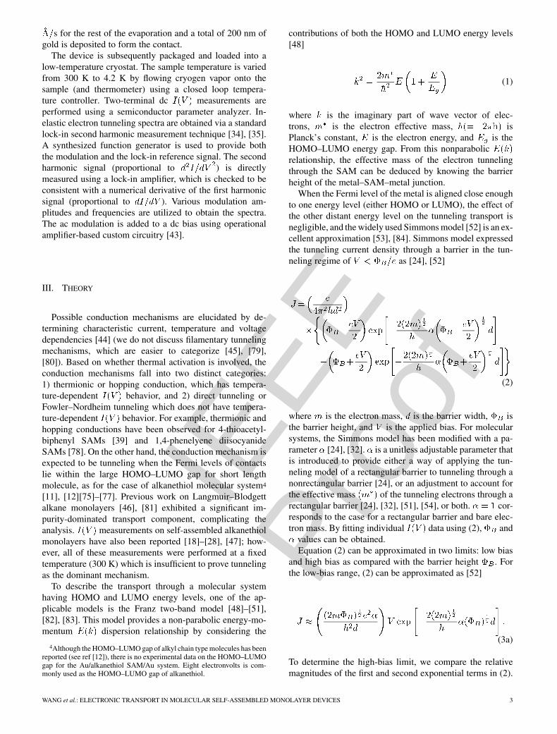
Fig. 3. Log plot of tunneling current densities multiplied by molecularlength d at low bias and by d at high bias (symbols) versus molecularlengths. The lines through the data points are linear fittings.
hundred different pairs were used in the fittingswith ranging from 1.0 to 2.5 eV (0.01 eV increment) and
from 0.5 to 1.0 (0.01 increment). Fig. 2 is a representativecontour plot of versus and values generatedfor the C12 data where darker regions correspond tosmaller and various shades represent half orderof magnitude steps. The darker regions representbetter fits of (2) to the measured data. In the inset,one can see there is a range of possible and valuesyielding minimum fitting parameters. Although the tun-neling parameters determined from the previous Simmonstunneling fitting eV and lie withinthis minimum region in this figure, there is a distribution ofother possible values.
Three alkanethiols of different molecular length, C8, C12,and C16, were investigated to study length-dependent tun-neling behavior. Fig. 3 is a semilog plot of tunneling currentdensities multiplied by molecular length ( at low bias and
at high bias) as a function of the molecular length forthese alkanethiols. The molecular lengths used in this plotare 13.3, 18.2, and 23.2 for C8, C12, and C16, respectively.Each molecular length was determined by adding an Au-thiolbonding length to the length of molecule [21]. Note that theselengths assume through-bond tunneling [21], [22], [31], [55],[85]. The high- and low-bias regimes are defined somewhatarbitrarily by comparing the relative magnitudes of the firstand second exponential terms in (2). Using eVand obtained from nonlinear least squares fitting ofthe C12 data, the second term becomes less than 10%of the first term at 0.5 V that is chosen as the boundary oflow- and high-bias ranges. As seen in Fig. 3, the tunnelingcurrent shows exponential dependence on molecular length,which is consistent with the Simmons tunneling model (3).The values can be determined from the slope at each biasand are plotted in Fig. 4. The error bar of an individualvalue in this plot was obtained by considering both the devicesize uncertainties and the linear fitting errors. The determined
values are almost independent of bias in the low-bias range
WANG et al.: ELECTRONIC TRANSPORT IN MOLECULAR SELF-ASSEMBLED MONOLAYER DEVICES 5

IEEE
Proo
f
Fig. 4. Plot of � versus bias in the low-bias range (square symbols) andhigh-bias ranges (circular symbols). The inset shows a plot of � versusbias with a linear fitting.
Table 1Summary of Alkanethiol Tunneling Parameters in This Study
V , and an average of in thisregion (from 0 to 0.5 V) can be calculated from Fig. 4.
The value ( permethylene) for alkanethiols reported here and summarizedin Table 1 is comparable to previously reported values. This
value agrees with the value of 0.79 calculatedvia (4a) from fitting individual characteristic of theC12 device. The calculated of C8 and C16 devices alsohave similar values, as summarized in Table 1.
According to (4b), depends on bias linearly in thehigh-bias range. The inset in Fig. 4 is a plot of versusin this range (0.5–1.0 V) along with linear fitting of the data.From this fitting, eV andwere obtained from the intercept and the slope, respectively,consistent with the values eV andobtained from the nonlinear least squares fitting in the pre-vious section.
values for alkanethiols obtained by various experimentaltechniques have previously been reported [18]–[32], [47]. Inorder to compare with these reported values, we also per-formed length-dependent analysis on our experimental dataaccording to the generally used equation [19]–[27], [32]:
(5)
This gives a value from 0.84 to 0.73\ in the biasrange from 0.1 to 1.0 V, which is comparable to resultsreported previously. For example, Holmlin et al. reporteda value of 0.87 by mercury drop experiments [24];and Wold et al. have reported of 0.94 and Cui et al.reported of 0.64 for various alkanethiols by using aconducting atomic force microscope technique [20], [22].These reported were treated as bias-independent quanti-ties, contrary to the results that are reported here and thatwere observed [AU: OK as edited?]in a slightlydifferent alkane system (ligand-encapsulated nanopar-ticle/alkane-dithiol molecules) [23]. We also caution againstthe use of parameters that have not been checked with atemperature-dependent analysis, since small non-tunnelingcomponents can dramatically affect derived values of .
We have analyzed our experimental data using a Franztwo-band model [48]–[51], [82], [83]. Since there is noreliable experimental data on the Fermi level alignment inthese metal–SAM–metal systems, and are treatedas adjustable parameters. We performed a least squaresfit on our data with the Franz nonparabolic rela-tionship [(1)] using an alkanethiol HOMO–LUMO gapof 8 eV5 [12], [75]–[77]. The best fitting parameters ob-tained by minimizing were eV and
m, where the error ranges of andare dominated by the error fluctuations of .Both electron tunneling near the LUMO and hole tunnelingnear the HOMO can be described by these parameters.
eV indicates that the Fermi level is aligned closeto one energy level in either case; therefore, the Simmonsmodel is a valid approximation. The and valuesobtained here are in reasonable agreement with the previousresults obtained from the Simmons model.
B. Inelastic Electron Tunneling Spectroscopy
Electronic transport through alkanethiol SAMs is furtherinvestigated with the technique of inelastic electron tunnelingspectroscopy [33], such as the works of 1966 by Jaklevic andLambe, who studied the conductance of a tunnel junctionswith encased organic molecules [34]. Since then it has be-come a powerful spectroscopic tool for chemical identifica-tion, chemical bonding investigation, and surface chemistryand physics studies [37]. In an inelastic tunneling process,the electron loses energy to a localized vibrational mode witha frequency when the applied bias satisfies the conditionof eV As a result, an additional tunneling channelis opened for the electron, resulting in an increase in thetotal current at the applied bias corresponding to the vibra-tional mode energy [36]. Typically only a small fraction oftunneling electrons are involved in the inelastic tunnelingprocess (determined by the electron—vibronic mode cou-pling coefficient), resulting in a small conductance change,which is commonly measured in the second harmonics of
5Although the HOMO–LUMO gap of alkyl chain type molecules has beenreported (see ref [12]), there is no experimental data on the HOMO–LUMOgap for the Au/alkanethiol SAM/Au system. Eight electronvolts is com-monly used as the HOMO–LUMO gap of alkanethiol.
6 PROCEEDINGS OF THE IEEE, VOL. 93, NO. 10, OCTOBER 2005

IEEE
Proo
f
a phase-sensitive detector that yields the characteristic fre-quencies of the corresponding vibrational modes as well asother information [35]–[37].
measurements and additional IETS studies havebeen performed on an octanedithiol (C8-dithiol) SAM usingthe aforementioned device structure [33]. The datafor this device was obtained from 300 K to 4.2 K. An Ar-rhenius plot shown in Figure [AU: Please specifyfigure]exhibits no temperature dependence, verifying thattunneling is the main transport mechanism for C8-dithiolSAM. This result is in good agreement with the tunnelingtransport characteristics observed previously. Using a junc-tion area of 51 5 nm in diameter (obtained from statis-tical studies of the nanopore size with SEM), a current den-sity of 9.3 1.8 10 A/cm at 1.0 V is calculated. As acomparison, the current density of 3.1 1.0 10 A/cmat 1.0 V was observed for C8 monothiol SAM. Using themodified Simmons model (2), the transport parameters of
eV and mwere obtained for this C8-dithiol SAM.
Figure 11[AU: Please provide correct figurereference] shows the IETS spectrum of the sameC8-dithiol SAM device obtained at K. An acmodulation of 8.7 mV (rms value) at a frequency of 503 Hzwas applied to the sample to acquire the second harmonicsignals. The spectra are stable and repeatable upon succes-sive bias sweeps. The spectrum at 4.2 K is characterized bythree pronounced peaks in the 0–200 mV region at 33, 133,and 158 mV. From comparison with previously reported IR,Raman, and high resolution electron energy loss (HREEL)spectra of SAM-covered gold surfaces, these three peaks areassigned to Au S , C C , and CH modes ofa surface-bound alkanethiolate6 [58]–[60]. The absence of astrong S H signal at 329 mV suggests that most ofthe thiol groups have reacted with the gold bottom and topcontacts. Peaks are also reproducibly observed at 80, 107,and 186 mV. They correspond to C S , CH , and
CH modes. The stretching mode of the CH groups,CH , appears as a shoulder at 357 meV. The peak at 15
mV is due to vibrations from either Si, Au, or C C C[61], [86], [87]. We note that all alkanethiolate peaks withoutexception or omission occur in the spectra. Peaks at 58, 257,277, and 302 mV, as well as above 375 mV are likely to orig-inate from Si–H and N–H vibrations related to the siliconnitride membrane [61], [62], [88], which forms the SAMencasement. To the best of our knowledge, alkanethiols haveno vibrational signatures in these regions. Measurement ofthe background spectrum of an “empty” nanopore devicewith only gold contacts to obtain background contributionsfrom Si N is hampered by either too low (open circuit) ortoo high (short circuit) currents in such a device. SimilarIETS result has also been obtained using a different teststructure recently [63].
6The symbols �, , and � denote in-plane rocking (r) and scissoring (s),out-of-plane wagging (w) and twisting (t), and stretching modes, respec-tively.
Fig. 5. Inelastic electron tunneling spectrum of C8 dithiol SAM obtainedfrom lock-in second harmonic measurement with an ac modulation of 8.7mV (rms value) at a frequency of 503 Hz (T = 4:2 K). Peaks labeled � aremost probably background due to the encasing Si N .
Although there are no selection rules in IETS as there arein IR and Raman spectroscopy, certain selection preferenceshave been established. According to the IETS theory [64],molecular vibrations with net dipole moments perpendic-ular to the interface of the tunneling junction have strongerpeak intensities than vibrations with net dipole moments par-allel to the interface (for dipoles close to the electrodes).Thus vibrations perpendicular to the electrode interface, i.e.,
Au S , C S , C C , and CH , dominate theIETS spectrum, while modes parallel to the interface, i.e.,
CH and CH , are weak, as shown in Fig. 4.In order to verify that the observed spectra are indeed
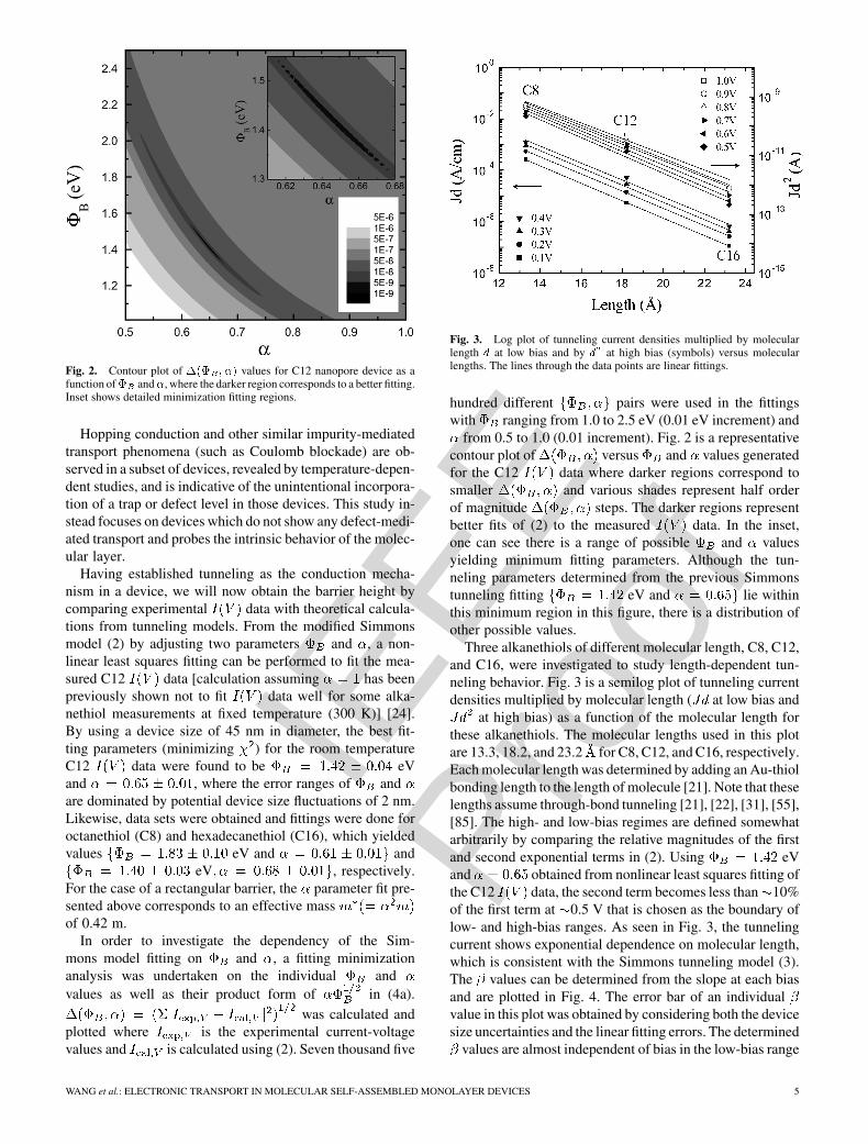
valid IETS data, the peak width broadening was examinedas a function of temperature and modulation voltage. IETSwas performed with different ac modulations at a fixedtemperature, and at different temperatures with a fixed acmodulation. Fig. 5(a) shows the modulation dependence ofthe IETS spectra obtained at 4.2 K, and Fig. 5(b) showsthe modulation broadening of the C–C stretching mode at133 meV. The circular symbols are the full widths at halfmaximum (FWHMs) of the experimental peak at Kwith various modulation voltages. A Gaussian distributionfunction was utilized to obtain a FWHM and the errorrange [65]. The square symbols are calculated FWHMvalues taking into account both a finite tem-perature effect kBT [35] and a finitevoltage modulation effect V[66]. These two broadening contributions add as the squares
. The agreement isexcellent over most of the modulation range, but we note asaturation of the linewidth at low modulation bias, indicatingthe influence of a non-negligible intrinsic linewidth. Takinginto account the known thermal and modulation broaden-ings, and including the intrinsic linewidth [67] as a
WANG et al.: ELECTRONIC TRANSPORT IN MOLECULAR SELF-ASSEMBLED MONOLAYER DEVICES 7
IEEE
Proo
fFig. 6. (a) Modulation dependence of IETS spectra obtained at 4.2 K. (b)Line (C-C stretching mode) broadening as a function of ac modulation. Thecircular symbols are experimental FWHMs, and the square symbols are the-oretical calculations considering both modulation and thermal contributions.The shaded bar denotes the expected saturation due to the derived intrinsiclinewidth (including a 5.4 k T thermal contribution) of 3.73 � 0.98 meV.
fitting parameter, the measured peak width is givenby
(6)
can be determined by using a nonlinear least squares fitto the ac modulation data (Fig. 12)[AU: Please pro-vide correct figure reference] with (6), giving anintrinsic linewidth of 3.73 0.98 meV for this line. This isshown (with the error range) in Fig. 5(b) as a shaded bar, in-cluding the thermal contribution.
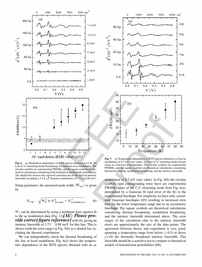
We can independently check the thermal broadening ofthe line at fixed modulation. Fig. 6(a) shows the tempera-ture dependence of the IETS spectra obtained with an ac
Fig. 7. (a) Temperature dependence of IETS spectra obtained at a fixed acmodulation of 8.7 mV (rms value). (b) Line (C-C stretching mode) broad-ening as a function of temperature. The circular symbols are experimentalFWHMs, and the square symbols are theoretical calculations consideringthermal broadening, modulation broadening, and the intrinsic linewidth.
modulation of 8.7 mV (rms value). In Fig. 6(b) the circularsymbols (and corresponding error bars) are experimentalFWHM values of the C-C stretching mode from Fig. 6(a),determined by a Gaussian fit (and error of the fit) to theexperimental lineshape. For simplicity we have only consid-ered Gaussian lineshapes [65] resulting in increased errorbars for the lower temperature range due to an asymmetriclineshape. The square symbols are theoretical calculationsconsidering thermal broadening, modulation broadening,and the intrinsic linewidth determined above. The errorranges of the calculation (due to the intrinsic linewidtherror) are approximately the size of the data points. Theagreement between theory and experiment is very good,spanning a temperature range from below ( 0.5) to above( 10) the thermally broadened intrinsic linewidth. Thislinewidth should be a sensitive test to compare to theoreticalmodels of transmission probabilities [68].
8 PROCEEDINGS OF THE IEEE, VOL. 93, NO. 10, OCTOBER 2005

IEEE
Proo
f
[AU: Please provide in-text figure refer-ence to Fig. 7]Similar intrinsic linewidths have beendetermined for the Au–S stretching mode (33 meV) and theCH wagging mode (158 meV). For the Au-S stretchingmode, the deviation of experimental data from calculatedvalues (thermal and modulation width only) is little, in-dicating that its intrinsic linewidth is small. A linewidthupper limit of 1.69 meV is determined for this vibrationalmode. For the CH wagging mode, a nonlinear least squaresfit to (6) gave an intrinsic linewidth of 13.5 2.4 meV.The linewidths and their variation throughout the moleculeare potentially due to inhomogeneous configuration of themolecular constituents, and a more detailed understandingmay give detailed structural information of these devicestructures.
V. CONCLUSION
We present here a study of electron tunneling through alka-nethiol SAMs, with the intent that this system can serve asa simple standard for the development of well-characterizedmolecular junctions. The characteristics are consistent withaccepted models of MIM tunneling junctions, as well as pre-senting a system on which tunneling spectroscopy can be per-formed.
The field of “molecular electronics” is rich in the proposaland promise of numerous device concepts [69], [70], but un-fortunately has an absence of reliable data and characteri-zation techniques upon which to test these ideas. It is in-cumbent upon the experimentalist to carefully institute con-trols to carefully validate claims of intrinsic molecular be-havior. Systematic controls, such as the model system pre-sented here, should assist in guiding further work toward arational development of the fascinating device structures andsystems that the field promises.
ACKNOWLEDGMENT
The authors would like to thank J. F. Klemic, X. Li, andR. Munden for helpful discussions and assistance. The au-thors especially thank I. Kretzschmar for assistance in iden-tification of the IETS spectra.
REFERENCES
[1] [AU: Throughout, please provideall paper titles and vol. numbers asneeded]M. A. Reed and J. M. Tour, Sci. Amer., pp. 86–93,June 2000.
[2] M. A. Reed, C. Zhou, C. J. Muller, T. P. Burgin, and J. M. Tour,Science, vol. 278, pp. 252–254, 1997.
[3] M. A. Reed and T. Lee Eds., Molecular Nanoelec-tronics Stevenson Ranch, CA: American Scientific, 2003.
[4] J. R. Heath and M. A. Ratner, Phys. Today, pp. 43–49, May 2003.[5] Y. Chen, G.-Y. Jung, D. A. A. Ohlberg, X. Li, D. R. Stewart, J.
O. Jeppesen, K. A. Nielsen, J. F. Stoddart, and R. S. Williams,Nanotechnology, vol. 14, pp. 462–468, 2003.
[6] Y. Luo, C. P. Collier, J. O. Jeppesen, K. A. Nielsen, E. DeIonno,G. Ho, J. Perkins, H.-R. Tseng, T. Yamamoto, J. F. Stoddart, andJ. R. Heath, Chem. Phys. Chem., vol. 3, pp. 519–525, 2002.
[7] D. R. Stewart, D. A. A. Ohlberg, P. A. Beck, Y. Chen, R. S.Williams, J. O. Jeppesen, K. A. Nielsen, and J. F. Stoddart, NanoLett., vol. 4, pp. 133–136, 2004.
[8] T. Lee, W. Wang, J. F. Klemic, J. J. Zhang, J. Su, and M. A.Reed, J. Phys. Chem. B, vol. 108, pp. 8742–8750, 2004.
[9] A. Ulman, An Introduction to Ultrathin Organic Films from Lang-muir–Blodgett to Self-Assembly. Boston, MA: Academic, 1991.
[10] G. E. Poirier, Chem. Rev., vol. 97, pp. 1117–1127, 1997.[11] M. A. Ratner, B. Davis, M. Kemp, V. Mujica, A. Roitberg, and
S. Yaliraki, Molecular Electronics: Science and Technology, TheAnnals of the New York Academy of Sciences A. Aviram and M.Ratner Eds. New York: New York Academy of Sciences, 1998,vol. 852.
[12] C. Boulas, J. V. Davidovits, F. Rondelez, and D. Vuillaume,Phys. Rev. Lett., vol. 76, pp. 4797–4800, 1996.
[13] M. W. Walczak, C. Chung, S. M. Stole, C. A. Widrig, and M. D.Porter, J. Amer. Chem. Soc., vol. 113, pp. 2370–2378, 1991.
[14] R. G. Nuzzo, B. R. Zegarski, and L. H. Dubois, J. Amer. Chem.Soc., vol. 109, pp. 733–740, 1987.
[15] C. A. Widrig, C. Chung, and M. D. Porter, J. Electroanal. Chem.,vol. 310, pp. 335–359, 1991.
[16] G. E. Poirier and M. J. Tarlov, Langmuir, vol. 10, pp. 2853–2856,1994.
[17] M. D. Porter, T. B. Bright, D. L. Allara, and C. E. D. Chidsey, J.Amer. Chem. Soc., vol. 109, pp. 3559–3568, 1987.
[18] L. A. Bumm, J. J. Arnold, T. D. Dunbar, D. L. Allara, and P. S.Weiss, J. Phys. Chem. B, vol. 103, pp. 8122–8127, 1999.
[19] B. Xu and N. J. Tao, Science, vol. 301, pp. 1221–1223, 2003.[20] D. J. Wold and C. D. Frisbie, J. Amer. Chem. Soc., vol. 123, pp.
5549–5556, 2001.[21] D. J. Wold, R. Haag, M. A. Rampi, and C. D. Frisbie, J. Phys.
Chem. B, vol. 106, pp. 2813–2816, 2002.[22] X. D. Cui, X. Zarate, J. Tomfohr, O. F. Sankey, A. Primak, A.
L. Moore, T. A. Moore, D. Gust, G. Harris, and S. M. Lindsay,Nanotechnology, vol. 13, pp. 5–14, 2002.
[23] X. D. Cui, A. Primak, X. Zarate, J. Tomfohr, O. F. Sankey, A.L. Moore, T. A. Moore, D. Gust, L. A. Nagahara, and S. M.Lindsay, J. Phys. Chem. B, vol. 106, pp. 8609–8614, 2002.
[24] R. Holmlin, R. Haag, M. L. Chabinyc, R. F. Ismagilov, A. E.Cohen, A. Terfort, M. A. Rampi, and G. M. Whitesides, J. Amer.Chem. Soc., vol. 123, pp. 5075–5085, 2001.
[25] M. A. Rampi and G. M. Whitesides, Chem. Phys., vol. 281, pp.373–391, 2002.
[26] K. Slowinski, H. K. Y. Fong, and M. Majda, J. Amer. Chem. Soc.,vol. 121, pp. 7257–7261, 1999.
[27] R. L. York, P. T. Nguyen, and K. Slowinski, J. Amer. Chem. Soc.,vol. 125, pp. 5948–5953, 2003.
[28] J. G. Kushmerick, D. B. Holt, S. K. Pollack, M. A. Ratner, J. C.Yang, T. L. Schull, J. Naciri, M. H. Moore, and R. Shashidhar,J. Amer. Chem. Soc., vol. 124, pp. 10654–10655, 2002.
[29] J. F. Smalley, S. W. Feldberg, C. E. D. Chidsey, M. R. Lin-ford, M. D. Newton, and Y. Liu, J. Phys. Chem., vol. 99, pp.13141–13149, 1995.
[30] K. Weber, L. Hockett, and S. Creager, J. Phys. Chem. B, vol. 101,pp. 8286–8291, 1997.
[31] K. Slowinski, R. V. Chamberlain, C. J. Miller, and M. Majda, J.Amer. Chem. Soc., vol. 119, pp. 11910–11919, 1997.
[32] W. Wang, T. Lee, and M. A. Reed, Phys. Rev. B, vol. 68, p.035416, 2003.
[33] W. Wang, T. Lee, I. Kretzschmar, and M. A. Reed, Nano Lett.,vol. 4, pp. 643–646, 2004.
[34] R. C. Jaklevic and J. Lambe, Phys. Rev. Lett., vol. 17, pp.1139–1140, 1966.
[35] J. Lambe and R. C. Jaklevic, Phys. Rev., vol. 165, pp. 821–832,1968.
[36] C. J. Adkins and W. A. Phillips, J. Phys. C: Solid State Phys., vol.18, pp. 1313–1346, 1985.
[37] P. K. Hansma Ed., Tunneling Spectroscopy: Capabilities, Appli-cations, and New Techniques New York: Plenum, 1982.
[38] B. C. Stipe, M. A. Rezaei, and W. Ho, Science, vol. 280, pp.1732–1735, 1998.
[39] C. Zhou, M. R. Deshpande, M. A. Reed, L. Jones II, and J. M.Tour, Appl. Phys. Lett., vol. 71, pp. 611–613, 1997.
[40] J. Chen, M. A. Reed, A. M. Rawlett, and J. M. Tour, Science,vol. 286, pp. 1550–1552, 1999.
[41] K. S. Ralls, R. A. Buhrman, and R. C. Tiberio, Appl. Phys. Lett.,vol. 55, pp. 2459–2461, 1989.
[42] R. M. Metzger, B. Chen, U. Holpfner, M. V. Lakshmikantham,D. Vuillaume, T. Kawai, X. Wu, H. Tachibana, T. V. Hughes, H.Sakurai, J. W. Baldwin, C. Hosch, M. P. Cava, L. Brehmer, andG. J. Ashwell, J. Amer. Chem. Soc., vol. 119, pp. 10455–10466,1997.
WANG et al.: ELECTRONIC TRANSPORT IN MOLECULAR SELF-ASSEMBLED MONOLAYER DEVICES 9

IEEE
Proo
f
[43] P. Horowitz and W. Hill, The Art of Electronics. New York:Cambridge Univ. Press, 1989.
[44] S. M. Sze, Physics of Semiconductor Devices. New York: Wiley,1981.
[45] R. E. Thurstans and D. P. Oxley, J. Phys. D: Appl. Phys., vol. 35,pp. 802–809, 2002.
[46] B. Mann and H. Kuhn, J. Appl. Phys., vol. 42, pp. 4398–4405,1971.
[47] F. F. Fan, J. Yang, L. Cai, D. W. Price, S. M. Dirk, D. V.Kosynkin, Y. Yao, A. M. Rawlett, J. M. Tour, and A. J. Bard,J. Amer. Chem. Soc., vol. 124, pp. 5550–5560, 2002.
[48] W. Franz, Handbuch der Physik S. Flugge Ed. Berlin, Germany:Springer-Verlag, 1956, vol. 17, p. 155.
[49] G. Lewicki and C. A. Mead, Phys. Rev. Lett., vol. 16, pp. 939–941,1966.
[50] B. Brar, G. D. Wilk, and A. C. Seabaugh, Appl. Phys. Lett., vol.69, pp. 2728–2730, 1996.
[51] C. Joachim and M. Magoga, Chem. Phys., vol. 281, pp. 347–352,2002.
[52] J. G. Simmons, J. Appl. Phys., vol. 34, pp. 1793–1803, 1963.[53] ——, J. Phys. D, vol. 4, pp. 613–657, 1971.[54] J. K. Tomfohr and O. F. Sankey, Phys. Rev. B, vol. 65, p. 245105,
2002.[55] H. Yamamoto and D. H. Waldeck, J. Phys. Chem. B, vol. 106, pp.
7469–7473, 2002.[56] C.-C. Kaun and H. Guo, Nano Lett., vol. 3, pp. 1521–1525, 2003.[57] S. Piccinin, A. Selloni, S. Scandolo, R. Car, and G. Scoles, J.
Chem. Phys., vol. 119, pp. 6729–6735, 2003.[58] M. A. Bryant and J. E. Pemberton, J. Amer. Chem. Soc., vol. 113,
pp. 8284–8293, 1991.[59] H. S. Kato, J. Noh, M. Hara, and M. Kawai, J. Phys. Chem. B,
vol. 106, pp. 9655–9658, 2002.[60] C. Castiglioni, M. Gussoni, and G. Zerbi, J. Chem. Phys., vol. 95,
pp. 7144–7149, 1991.[61] M. Molinari, H. Rinnert, M. Vergnat, and P. Weisbecker, Mater.
Sci. Eng. B, vol. 101, p. 186, 2003.[62] U. Mazur and K. W. Hipps, J. Phys. Chem., vol. 85, pp.
2244–2249, 1981.[63] J. G. Kushmerick, J. Lazorcik, C. H. Patterson, R. Shashidhar,
D. S. Seferos, and G. C. Bazan, Nano Lett., vol. 4, pp. 639–642,2004.
[64] J. Kirtley and J. T. Hall, Phys. Rev. B, vol. 22, pp. 848–856, 1980.[65] I. J. Lauhon and W. Ho, Phys. Rev. B, vol. 60, pp. R8525–R8528,
1999.[66] J. Klein, A. Leger, M. Belin, D. Defourneau, M. J. L. Sangster,
and , Phys. Rev. B, vol. 7, pp. 2336–2348, 1973.[67] L. J. Lauhon and W. Ho, Rev. Sci. Instrum., vol. 72, pp. 216–223,
2001.[68] M. A. Kastner, Phys. Today, Jan. 24–31, 1993.[69] A. Aviram and M. Ratner Eds., Molecular Electronics: Science
and Technology, The Annals of the New York Academy of Sci-ences New York: New York Academy of Sciences, 1998, vol.852.
[70] J. Reimers, C. Picconatto, J. Ellenbogen, and R. Shashidhar,Molecular Electronics III, The Annals of the New York Academyof Sciences. New York: New York Academy of Sciences, 2003,vol. 1006.
[71] A. Nitzan and M. A. Ratner, Science, vol. 300, pp. 1384–1389,2003.
[72] Hewlett-Packard Quantum Science Research, “Beyond silicon:Breakthroughs in molecular electronics,” [Online]. Available:http://www.hpl.hp.com/research/qsr/
[73] C. P. Collier, G. Mattersteig, E. W. Wong, Y. Luo, K. Beverly, J.Sampaio, F. M. Raymo, J. F. Stoddart, and J. R. Heath, Science,vol. 289, pp. 1172–1175, 2000.
[74] C. N. Lau, D. R. Stewart, R. S. Williams, and M. Bockrath, NanoLett., vol. 4, pp. 569–572, 2004.
[75] M. Fujihira and H. Inokuchi, Chem. Phys. Lett., vol. 17, pp.554–556, 1972.
[76] S. G. Lias, J. E. Bartmess, J. F. Liebman, J. L. Holmes, R. D.Levin, and W. G. Mallard, “Gas-phase ion and neutral thermo-chemistry,” J. Phys. Chem. Ref. Data, vol. 17, no. 1, p. 24, 1998.
[77] H.-H. Yang and R. L. McCreery, Anal. Chem., vol. 71, p. 4081,1999.
[78] J. Chen, L. C. Calvet, M. A. Reed, O. W. Carr, D. S. Grubisha,and D. W. Bennett, Chem. Phys. Lett., vol. 313, pp. 741–748, 1999.
[79] J. G. Simmons and R. R. Verderber, Prof. Roy. Soc. A., vol. 301,pp. 77–102, 1967.
[80] G. Dearnaley, A. M. Stoneham, and D. V. Morgan, Rep. Prog.Phys., vol. 33, pp. 1129–1191, 1970.
[81] E. E. Polymeropoulos and J. Sagiv, J. Chem. Phys., vol. 69, pp.1836–1847, 1978.
[82] R. Stratton, G. Lewicki, and C. A. Mead, J. Phys. Chem. Solids,vol. 27, pp. 1599–1604, 1966.
[83] G. H. Parker and C. A. Mead, Phys. Rev. Lett., vol. 21, pp.605–607, 1968.
[84] J. Maserjian and G. P. Petersson, Appl. Phys. Lett., vol. 25, pp.50–52, 1974.
[85] A. M. Napper, H. Liu, and D. H. Waldeck, J. Phys. Chem. B, vol.105, pp. 7699–7707, 2001.
[86] P. D. Bogdanoff, B. Fultz, and S. Rosenkranz, Phys. Rev. B, vol.60, pp. 3976–3981, 1999.
[87] U. Mazur and K. W. Hipps, J. Phys. Chem., vol. 86, pp.2854–2860, 1982.
[88] H. Kurata, M. Hirose, and Y. Osaka, Jpn. J. Appl. Phys., vol. 20,p. L811, 1981.
Wenyong Wang received the B.S. degree fromNankai University, China, and the Ph.D. degreein physics from Yale University, New Haven, CT.
Currently he is a Guest Researcher at theSemiconductor Electronics Division of theNational Institute of Standards and Technology,Gaithersburg, MD. His research work focuseson the electrical characterizations of chargetransport in nanometer-scale device structures.
Takhee Lee received the Ph.D. degree in physicsfrom Purdue University, West Lafeyettte, IN, in2000.
Between 2000 and 2004, he was a Postdoc-toral Associate in the Department of ElectricalEngineering, Yale University, New Haven, CT.Since 2004, he has been an Assistant Professorin the Department of Materials Science AndEngineering, Gwangju Institute of Science andTechnology (GIST), Gwangju, Korea. His re-search interest is characterization of the electrical
and structural properties of nanostructures involving single molecules,nanoparticles, nanowires, and their assembly for electronic applications.
Mark A. Reed received the B.S. (with honors)and M.S. degrees in physics and the Ph.D. degreein solid-state physics from Syracuse University,Syracuse, NY, in 1977, 1979, and 1983, respec-tively.
He then joined Texas Instruments as aMember of the Technical Staff in the UltrasmallElectronics Branch, where he cofounded theNanoelectronics research program. In 1988, hebecame a Senior Member of the Technical Staff.In 1990, he left TI to join the faculty at Yale
University, New Haven, CT, where he currently holds a joint appointment asProfessor in the Electrical Engineering and Applied Physics Departments.From 1995 to 2001, he served as the Chairman of Electrical Engineering,where his teaching interests include outreach of technology to nonsciencestudents and mentoring promising young talent, including the nationalwinners of the Intel, Westinghouse, and STS science competitions. He is theauthor of more than 150 professional publications and six books, has given15 plenary and over 240 invited talks, and holds 24 U.S. and foreign patentson quantum effect, heterojunction, and molecular devices. His books creditsinclude Nanostructure Physics and Fabrication (1989), Nanostructuresand Mesoscopic Systems (1992), Nanostructured Systems (in the seriesSemiconductors and Semimetals), Molecular Electronics (2001), and
Molecular Nanolectronics (2003) [AU: Please provide
10 PROCEEDINGS OF THE IEEE, VOL. 93, NO. 10, OCTOBER 2005

IEEE
Proo
f
publishers and city and state/country lo-cations]. He has chaired numerous international conferences andprogram committees, and has served as an associate editor for a numberof technical journals (such as Physical Review Letters and Physica E). Hisresearch activities have included the investigation of nanoscale and meso-scopic systems, electronic transport in heterojunction systems, artificiallystructured materials and devices, microelectromechanical systems (MEMS)and bioMEMS, nanotechnology, and molecular electronics.
Dr. Reed has been elected to the Connecticut Academy of Science and En-gineering and Who’s Who in the World. His awards include Fortune maga-
zine’s “Most Promising Young Scientist” (1990), the Kilby Young InnovatorAward (1994), the DARPA ULTRA Most Significant Acheivement Award(1997), the Harold Hodgkinson Chair of Engineering and Applied Scienceat Yale University (1999), the Syracuse University Distinguished Alumniaward (2000), the Forbes magazine “E-Gang” (2001), and the Fujitsu ISCSQuantum Device Award (2001), the Yale Science and Engineering Associa-tion Award for Advancement of Basic and Applied Science (2002). In 2003,he was elected a Fellow of the American Physical Society.
WANG et al.: ELECTRONIC TRANSPORT IN MOLECULAR SELF-ASSEMBLED MONOLAYER DEVICES 11
Copyright © 2022 FDOKUMEN