EC8252-Electronic Devices
45
1 EC8252- ELECTRONIC DEVICES (2 Marks & 16 Marks) UNIT I SEMICONDUCTOR DIODE PART- A 1. What are semiconductors? The materials whose electrical property lies between those of conductors and insulators are known as Semiconductors. Ex germanium, silicon. It has two types. 1. Intrinsic semiconductor 2. Extrinsic semiconductor. 2. What are valence electrons? Electron in the outermost shell of an atom is called valence electron. 3.What is forbidden energy gap? The space between the valence and conduction band is said to be forbidden energy gap. 4.What are conductors? Give examples? Conductors are materials in which the valence and conduction band overlap each other so there is a swift movement of electrons which leads to conduction. Ex. Copper, silver. 5.What are insulators? Give examples? Insulators are materials in which the valence and conduction band are far away from each other. So no movement of free electrons and thus no conduction. Ex glass, plastic. 6. Give the energy band structure of Insulator. In Insulators there is a wide forbidden energy gap. So movement of valence electron from valence to conduction band is not possible.
-
Upload
khangminh22 -
Category
Documents
-
view
0 -
download
0
Transcript of EC8252-Electronic Devices
1
EC8252- ELECTRONIC DEVICES (2 Marks & 16 Marks)
UNIT I SEMICONDUCTOR DIODE
PART- A 1. What are semiconductors?
The materials whose electrical property lies between those of conductors and insulators are known as Semiconductors. Ex germanium, silicon.
It has two types.
1. Intrinsic semiconductor 2. Extrinsic semiconductor. 2. What are valence electrons?
Electron in the outermost shell of an atom is called valence electron.
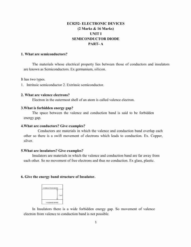
3.What is forbidden energy gap? The space between the valence and conduction band is said to be forbidden
energy gap.
4.What are conductors? Give examples? Conductors are materials in which the valence and conduction band overlap each
other so there is a swift movement of electrons which leads to conduction. Ex. Copper, silver.
5.What are insulators? Give examples? Insulators are materials in which the valence and conduction band are far away from
each other. So no movement of free electrons and thus no conduction. Ex glass, plastic.
6. Give the energy band structure of Insulator.
In Insulators there is a wide forbidden energy gap. So movement of valence electron from valence to conduction band is not possible.
2
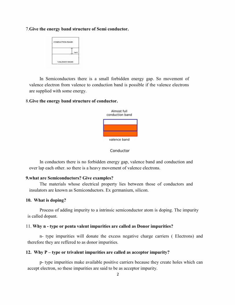
7.Give the energy band structure of Semi conductor.
In Semiconductors there is a small forbidden energy gap. So movement of valence electron from valence to conduction band is possible if the valence electrons are supplied with some energy.
8.Give the energy band structure of conductor.
In conductors there is no forbidden energy gap, valence band and conduction and over lap each other. so there is a heavy movement of valence electrons.
9.what are Semiconductors? Give examples? The materials whose electrical property lies between those of conductors and
insulators are known as Semiconductors. Ex germanium, silicon.
10. What is doping?
Process of adding impurity to a intrinsic semiconductor atom is doping. The impurity is called dopant.
11. Why n - type or penta valent impurities are called as Donor impurities?
n- type impurities will donate the excess negative charge carriers ( Electrons) and therefore they are reffered to as donor impurities.
12. Why P – type or trivalent impurities are called as acceptor impurity?
p- type impurities make available positive carriers because they create holes which can accept electron, so these impurities are said to be as acceptor impurity.

3
13. Give the expression for the Fermi level energy in n – type semiconductor.
EF = EC – kT ln NC/ ND
Where,
EF - Fermi level energy
EC – Conduction band energy
K – Boltzmann constant
T – Temperature
NC – dimension of concentration in n - type
ND - concentration of donor atoms
14.What is mobility? What is its unit?
Mobility of the charge carrier is defines as the average drift velocity per unit electricfield.
Its unit is meters per volt – seconds.
µ = v / E Where µ – mobility v – Drift velocity E – applied electric field
15. Define Conductivity.
Conductivity is defined as the current density per unit applied electric field.
Its unit is mho per meter
σ = J / E Where σ – Conductivity J- Current density E - applied electric field
16. Give the relationship between mobility and conductivity . σ = q n µ Where σ – Conductivity q- charge of electron n- concentration of electron
µ – Mobility
17. Define mean life time of a hole or and electron.
The electron hole pair created due to thermal agitation woll disappear as a result of recombination. Thus an average time for which a hole or an electron exist before recombination can be said as the mean life time of a hole or electron.
4
18. Differentiate between intrinsic and extrinsic semiconductor
INTRINSIC SEMICONDUCTORS
It is pure semi-conducting material and no
impurity atoms are added to it.
Examples: crystalline forms of pure silicon and
germanium.
The number of free electrons in the conduction
band and the no. of holes in valence band is
exactly equal and very small indeed.
Its electrical conductivity is low.
Its electrical conductivity is a function of
temperature alone.
EXTRINSIC SEMICONDUCTORS
It is prepared by doping a small quantity of impurity
atoms to the pure semi-conducting material.
Examples: silicon “Si” and germanium “Ge” crystals
with impurity atoms of As, Sb, P etc. or In B, Aℓ
etc.
The number of free electrons and holes is never
equal. There is excess of electrons in n-type semi-
conductors and excess of holes in p-type semi-
conductors.
Its electrical conductivity is high.
Its electrical conductivity depends upon the
temperature as well as on the quantity of impurity
atoms doped the structure.
19. Define drift current?
When an electric field is applied across the semiconductor, the holes move towards the negative terminal of the battery and electron move towards the positive ter mina of the battery. This drift movement of charge carriers will result in a current termed as drift current.
20. Give the expression for drift current density
Drift current density due to electrons
Jn = qn μnE
Where, Jn - drift current density due to electron q- Charge of electron
μn - Mobility of electron

5
E - applied electric field
Drift current density due to holes. Jp = q p μp E Where, Jn - drift current density due to holes q - Charge of holes μp - Mobility of holes
E - applied electric field
21. Define the term diffusion current? A concentration gradient exists, if the number of either electrons or holes is greater in one region of a semiconductor as compared to the rest of the region. The holes and electron tend to move from region of higher concentration to the region of lower concentration. This process in called diffusion and the current produced due this movement is diffusion current.
22. Give the expression for diffusion current density
Diffusion current density due to electrons
Jn = q Dn dn / dx
Where
Jn - diffusion current density due to electron q - Charge of an electron
Dn – diffusion constant for electron dn / dx – concentration gradient
Diffusion current density due to holes Jp = - q Dp dp / dx
Where
Jp - diffusion current density due to holes q - Charge of a hole
Dp – diffusion constant for hole dn / dx – concentration gradient
23. Differentiate between drift and diffusion currents.
Drift current
1. It is developed due to potential gradient.
2. This phenomenon is found both in metals and semiconductors
Diffusion current
1. It is developed due to charge concentration gradient.
2. This phenomenon is found only in metals

6
24. What is depletion region in PN junction?
The region around the junction from which the mobile charge carriers (electrons and holes) are depleted is called as depletion region. Since this region has immobile ions, which are electrically charged, the depletion region is also known as space charge region.
25. What is barrier potential?
Because of the oppositely charged ions present on both sides of PN junction an electric potential is established across the junction even without any external voltage source which is termed as barrier potential.
26. What is Reverse saturation current?
The current due to the minority carriers in reverse bias is said to be reverse saturation current. This current is independent of the value of the reverse bias voltage.
27. What is the total current at the junction of pn junction diode?
The total in the junction is due to the hole current entering the n material and the electron current entering the p material. Total current is given by
I = Ipn(0) + Inp(0)
Where,
I – Total current
Ipn(0) - hole current entering the n material
Inp(0) - electron current entering the p material
12.Give einstein’s relation?
28. Give the diode current equation? The diode current equation relating the voltage V and current I is given by
where I – diode current Io – diode reverse saturation current at room temperature
V – external voltage applied to the diode Ƞ - a constant, 1 for Ge and 2 for Si
VT = kT/q = T/11600, thermal voltage
K – Boltzmann’s constant (1.38066x10^-23 J/K) q – charge of electron (1.6x10^-19 C) T – temperature of the diode junction

7
29. What is recovery time? Give its types.
When a diode has its state changed from one type of bias to other a transient accompanies the diode response, i.e., the diode reaches steady state only after an interval of time “ tr” called as recovery time. The recovery time can be divided in to two types such as
(i) forward recovery time
(ii) reverse recovery time 30. Define storage time.
The interval time for the stored minority charge to become zero is called storage time. It is represented as ts.
31. Define transition time.
The time when the diode has normally recovered and the diode reverse current reaches reverse saturation current Io is called as transition time. It is represented as tt
32. Define PIV. Peak inverse voltage is the maximum reverse voltage that can be applied to the PN junction without damage to the junction.
33. Draw V-I characteristics of pn diode
34. Write the application of pn diode can be used as rectifier in DC Power Supplies.
In Demodulation or Detector Circuits.
In clamping networks used as DC Restorers
In clipping circuits used for waveform generation.
As switches in digital logic circuits.
In demodulation circuits.

8
35.What is the diffusion length for holes (Lp)?
Diffusion length of holes can be said as the mean distance of travel of hole before recombination.
Lp = ( Dp τp)1/2
36. What is forward bias and reverse bias in a PN junction?
When positive terminal of the external supply is connected to P region and negative terminal to N region ,the PN junction is said to be forward biased. under forward biased condition the PN region offers a very low resistance and a large amount of current flows through it
37. What is reverse bias in a PN junction?
When positive terminal of the external supply is connected to N type and negative terminal to P type then the PN junction is said to be in reverse bias. Under reverse biased condition the PN region offers a very high resistance and a small amount of current flows through it.
39. Define electron volt
One eV is the amount of energy acquired by an electron when it is accelerated through a potential difference of one volt (1v). the value of 1 ev is equal to 1.602*10-19 joule.
40.Define mass action law.
Under thermal equilibrium for any semi-conductor, the product of the no of holes & the no of electrons is constant & is independent of the amount of donor & acceptor impurity doping. This relation is known as mass-action law & is given by
n. p = ni2
41. What is the static resistance of a diode?
Static resistance R of a diode can be defined as the ratio of voltage V across the diode to the
current flowing through the diode.
R = V/ I
Where
R - Static resistance of a diode
V - Voltage across the diode

9
I - current across the diode
42. Define dynamic resistance.
Dynamic resistance of a diode can be defined as the ratio of change in voltage across the diode to the change in current through the diode.
r = V / I
Where
r - Dynamic resistance of a diode
V - change in voltage across the diode I - change in current through the diode
43. Define dynamic conductance. Dynamic conductance of a diode can be defined as the ratio of change in the change in current through the diode to the voltage across the diode. This can also be defined as the inverse of Dynamic resistance.
g = I / V = I + I0 / ή vT
Where
g - Dynamic conductance of a diode
V - change in voltage across the diode
I - change in current through the diode vT – threshold voltage
44. Define the term transition capacitance? When a PN junction is reverse biased, the depletion layer acts like a dielectric material while P and N –type regions on either side which has low resistance act as the plates. In this way a reverse biased PN junction may be regarded as parallel plate capacitor and thus the capacitance across this set up is called as the transition capacitance.
CT = εA / W
Where
CT - transition capacitance
ε - Permittivity of material A - Cross section area of the junction

10
W – Width of the depletion region
45.Define Alloy junction.
A junction formed experimentally in which there is an abrupt change from acceptor ions on one side to donor ions on the other side is called as an alloy or fusion junction.
46. Define Grown junction.
A junction obtained by drawing a single crystal from a melt of germanium whose type is changed during the drawing process by adding first P-type and then n –type impurity is called as grown junction.
47. Give the Poisson’s equation relating the potential and the charge density?
d2V / dx2 = e NA / ε
Where
V – Potential
e - Charge of the electron
NA – acceptor ion concentration
ε - Permittivity of material 48. What is a varactor diode? A diode which is based on the voltage variable capacitance of the reverse biased p-n junction is said to be varactor diode. It has other names such as varicaps, voltacaps.
49.Define the term diffusion capacitance.
The diffusion capacitance of a forward biased diode is defined as the rate of change of injected charge with voltage.
CD = τ I / ή VT
Where
τ – time constant I – current across the diode
vT – threshold voltage
50.Give the expression for charge control description of a diode. Charge control description of a diode can be given by
11
I = Q /τp
Where
I – current across the diode
Q – stored charge
τp - L2
p / Dp – life time for holes
51.what is recovery time? Give its types.
When a diode has its state changed from one type of bias to other a transient accompanies the diode response, i.e., the diode reaches steady state only after an interval of time “ tr” called as recovery time. The recovery time can be divided in to two types such as
(i) forward recovery time (ii) reverse recovery time 52.What is meant by forward recovery time? The forward recovery time may be defined as the time interval from the instant of 10% diode voltage to the instant this voltage reaches 90% of the final value. It is represented as t f
r.
53.What is meant by reverse recovery time?
The reverse recovery time can be defined as the time required for injected or the excess minority carrier density reduced to zero , when external voltage is suddenly reversed.
54.Define storage time.
The interval time for the stored minority charge to become zero is called storage time. It is represented as t s.
55. Define transition time.
The time when the diode has normally recovered and the diode reverse current reaches reverse saturaton current I0 is called as transition time. It is represented as t t
56. What are break down diodes?
Diodes which are designed with adequate power dissipation capabilities to operate in the break down region are called as break down or zener diodes.
57. What is break down? What are its types?
12
When the reverse voltage across the pn junction is increased rapidly at a voltage the junction breaks down leading to a current flow across the device. This phenomenon is called as break down and the voltage is break down voltage. The types of break down are
i) zener break down
ii)Avalanche breakdown
58. What is zener breakdown?
Zener breakdown takes place when both sides of junctions are very heavily doped.and the depletion layer will be thin.When a small value of reverse bias voltage is applied , a very strong electric field is set up across the thin depletion layer. This electric field is enough to break the covalent bonds. Now extremely large number of free charge carriers are produced which constitute the zener current. Thisprocess is known as zener break down.
59. What is avalanche break down?
When bias is applied , thermally generated carriers which are already present in the diode acquire sufficient energy from the applied potential to produce new carriers by removing valence electron from their bonds. These newly generated additional carriers acquire more energy from the potential and they strike the lattice and create more number of free electrons and holes. This process goes on as long as bias is increased and the number of free carriers get multiplied. This process is termed as avalanche multiplication. Thus the break down which occur in the junction resulting in heavy flow of current is termed as avalanche break down.
60. How does the avalanche breakdown voltage vary with temperature?
In lightly doped diode an increase in temperature increases the probability of collision of electrons and thus increases the depletion width. Thus the electrons and holes needs a high voltage to cross the junction. Thus the avalanche voltage is increased with increased temperature.
61. How does the zener breakdown voltage vary with temperature?
In heavily doped diodes, an increase in temperature increases the energies of valence electrons, and hence makes it easier for these electrons to escape from covalent bonds. Thus less voltage is sufficient to knock or pull these electrons from their position in the crystal and convert them in to conduction electrons. Thus zener break down voltage decreases with temperature.
62. Write applications of Zener diode
Zener diode is used as

13
(a) Voltage regulator (b) Voltage clipper circuits (c) For controlling the output amplitude.
PART B 1.Explain the drift and diffusion currents for PN diode. Pg no: (1.27-1.30) April 2015 (12 marks) 2.Derive the quantitative theory of PN diode currents. Pg.no : (1.46 – 1.48) (May 2014, Nov 2012, Nov 2011, June 2011 & 2010 ) 16 marks 3. Give diode current equation Pg.no : 1.48 4.Explain the operation of PN junction under reverse bias condition with its characteristics. Pg.no :1.39 (Nov 2014 & May 2013) 8 Marks
5. Explain the operation of PN junction under reverse bias condition with its characteristics.
Pg.no :1.39 & 1.40 (Nov 2014 & May 2013) 8 Marks
6. Explain the operation of PN junction as a Diode
Pg.no :1.40 & 1.41 (April 2015 & June 2011) 8 Marks
7. Explain details about the switching characteristics on PN diode with neat Sketch.
Pg.no :1.63 & 1.67 (Nov & May 2014) 8 Marks

14
UNIT II BIPOLAR JUNCTION
PART A
1. Why an ordinary transistor is called bipolar?
The operation of the transistor depends on both majority and minority carriers. So it is called bipolar device.
2. Collector region of transistor is larger than emitter. Why?
Collector is made physically larger than emitter and base because collector is to dissipate much power.
3. Why BJT is called current controlled device?
The output voltage, current, or power is controlled by the input current in a transistor. So it is called the current controlled device.
4. Define Early Effect. A variation of the base-collector voltage results in a variation of the quasi-neutral width in the base. The gradient of the minority-carrier density in the base therefore changes, yielding an increased collector current as the collector-base current is increased. This effect is referred to as the early effect.
5. Draw the characteristics of CE configuration.

15
6. Among CE, CB, CC which one is most popular. Why?
CE is most popular among the three because it has high gain compared to base and collector configuration. It has the gain about to 500 that finds excellent usage in audio frequency applications.
7. Compare CE, CB, CC.

16
8. Why h parameter model is important for BJT
It is important because:
1. Its values are used on specification sheets
2. It is one model that may be used to analyze circuit behavior
3. It may be used to form the basis of a more accurate transistor model 9. Define current amplification factor
In a transistor amplifier with a.c. input signal, the ratio of change in output current to be the change in input current is known as the current amplification factor.
9. Why h parameter model is important for BJT
It is important because:
1. Its values are used on specification sheets
2. It is one model that may be used to analyze circuit behavior
3. It may be used to form the basis of a more accurate transistor model
10. What do you meant by multi emitter transistor? Transistor–transistor logic (TTL) is a class of digital circuits built from bipolar junction transistors (BJT) and resistors. It is called transistor–transistor logic because both the logic gating function (e.g., AND) and the amplifying function are performed by transistors.
TTL is notable for being a widespread integrated circuit (IC) family used in many applications such as computers, industrial controls, test equipment and instrumentation, consumer electronics, synthesizers, etc.
11. In a CR connection, the value of IE is 6.28 mA and the collector current Ic is 6.20 mA.

17
Determine D.C. current gain.
12. The transistor has IE = 10 mA and α = 0.98. Find the value of base and collector
currents.
13. If a transistor has a α of 0.97 find the value of β. If β=200, find the value of α.

18
14. Give some applications of BJT.
The BJT remains a device that excels in some applications, such as discrete circuit design, due to the very wide selection of BJT types available, and because of its high transconductance and output resistance compared to MOSFETs.
The BJT is also the choice for demanding analog circuits, especially for very-high- frequency applications, such as radio-frequency circuits for wireless systems.
Bipolar transistors can be combined with MOSFETs in an integrated circuit by using a BiCMOS process of wafer fabrication to create circuits that take advantage of the application strengths of both types of transistor.
15. What is the major difference between a bipolar & unipolar device? In bipolar devices like BJT, the current flowing is controlled by both minority & majority charge carriers whereas in unipolar devices like FET, only the majority charge carriers are responsible for the current flow. 16. What is a transistor (BJT)?
Transistor is a three terminal device whose output current, voltage and /or power is controlled by input current.
17. What are the terminals present in a transistor?
Three terminals: emitter, base, collector.
19
PART B
1.Explain the operation of NPN and PNP transistors (16) Pg no : 2.2 – 2.5 (April 2015, Nov 2013 & May 2012) 2.Explain the input and output characteristics of a transistor in CB configuration. (10) Pg no : 2.5 – 2.8 (April 2015, Nov 2014 , May 2013 & June 2011) 3.Draw the circuit diagram of a NPN transistor CE configuration and the input and output characteristics. Also define its operating regions. (12)
Pg no : 2.8 – 2.12 (May 2015 & 2014 , Nov 2012 & June 2010) 4.Explain the input and output characteristics of a transistor in CC configuration. (10) Pg no : 2.12 – 2.13 5.Give the comparison of CE, CB, and CC configuration. (6) Pg no : 2.13 (May 2014 & 2013 , Nov 2012 & 2011) 6.Give the relationship between α, β and γ of a transistor (6) Pg no : 2.13 & 2.14
7. Explain briefly about the Gummel Poon model (10)
Pg no : 2.39 - 2.42
8. How multi emitter transistor is working? Explain it with neat diagram. (12)
Pg no :2.42 & 2.43
9. Explain details about the Ebers Moll model. (8)
Pg no : 2.29 & 2.30 (Nov 2014)

20
UNIT III FIELD EFFECT TRANSISTORS
PART A
1. Why it is called field effect transistor?
The drain current ID of the transistor is controlled by the electric field that extends into the
channel due to reverse biased voltage applied to the gate, hence this device has been given the name Field Effect Transistor.
2. Why FET is called voltage controlled device.
FET the value of the current depends upon the value of the voltage applied at the gate and drain. So it is known as voltage controlled device.
3. Define the term threshold voltage.
The threshold voltage, commonly abbreviated as Vth, of a field-effect transistor (FET) is the
value of the gate–source voltage when the conducting channel just begins to connect the source and drain contacts of the transistor, allowing significant current.
The threshold voltage of a junction field-effect transistor is often called pinch-off voltage instead, which is somewhat confusing since "pinch off" for an insulated-gate field-effect transistor is used to refer to the channel pinching that leads to current saturation behaviour under high source–drain bias, even though the current is never off. The term "threshold voltage" is unambiguous and refers to the same concept in any field-effect transistor.
4. What is channel length modulation?
One of several short-channel effects in MOSFET scaling, channel length modulation (CLM) is a shortening of the length of the inverted channel region with increase in drain bias for large drain biases.
As the drain voltage increases, its control over the current extends further toward the source, so the uninverted region expands toward the source, shortening the length of the channel region, the effect called channel-length modulation.
5.In which region JFET acts as a resistor & why ? When gate- source voltage , VGS = 0 , the depletion layer of the channel is very small & the JFET acts as a voltage controlled resistor since the current increases with increase in voltage

21
6. Draw the transfer characteristics curve for JFET.
7.Compare JFET with BJT.
8. Differentiate between N and P channel FETs
1. In an N channel JFET the current carriers are electrons, whereas the current carriers are

22
holes in a P channel JFET. 2. Mobility of electrons is large in N channel JFET; Mobility of holes is poor in P channel
JFET.
3. The input noise is less in N channel JFET than that of P channel JFET.
4. The transconductance is larger in N channel JFET than that of P channel JFET.
9. Write some applications for JFET.
10. Compare MOSFET with JFET.
11. Define pinch-off voltage.

23
In JFET, the electrons flow through a semiconducting channel between source & drain terminals. By applying a reverse bias voltager to a gate terminal, the channel is made free of charge carriers, ie., pinched off, so that the electrie current is impeded or switched off completely
12.What is FET?
FET is abbreviated for field effect transistor. It is a three terminal device with its outputcharacteristics controlled by input voltage.
13.Why FET is called voltage controlled device?
The output characteristics of FET is controlled by its input voltage thus it is voltage controlled.
14.What are the two main types of FET?
1. JFET 2. MOSFET.
15. What are the terminals available in FET?
1). Drain, 2).Source and 3). Gate
16. What is JFET?
JFET- Junction Field Effect Transistor.
17.What are the types of JFET?
N- Channel JFET and P- Channel JFET
18.What are the two important characteristics of JFET? a. Drain characteristics 2. Transfer characteristics.
19.What is transconductance in JFET?
It is the ratio of small change in drain current to the corresponding change in drain to source voltage.
20.What is amplification factor in JFET?

24
It is the ratio of small change in drain to source voltage to the corresponding change in Gate tosource voltage.
21. Why do we choose q point at the center of the loadline?
The operating point of a transistor is kept fixed usually at the center of the active region in order thatthe input signal is well amplified. If the point is fixed in the saturation region or the cut off region the positive and negative half cycle gets clipped off respectively.
22.List out the different types of biasing.
._ Voltage divider bias, Base bias, Emitter feed back bias, Collector feedback bias, Emitter bias.
23.What do you meant by thermal runway?
Due to the self heating at the collector junction, the collector current rises. This causes damage to thedevice. This phenomenon is called thermal runway.
24. Why is the transistor called a current controlled device?
The output characteristics of the transistor depend on the input current. So thtransistor is called acurrent controlled device.
25. Define current amplification factor?
It is defined as the ratio of change in output current to the change in input current at constant.
26.What are the requirements for biasing circuits?
The q point must be taken at the Centre of the active region of the output characteristics .• Stabilize the collector current against the temperature variations.
Make the q point independent of the transistor parameters. When the transistor is replaced, it must be of same type.
27.When does a transistor act as a switch?

25
The transistor acts as a switch when it is operated at either cutoff region or saturation
region
28.What is biasing?
To use the transistor in any application it is necessary to provide sufficient voltage and current tooperate the transistor. This is called biasing.
20. What is stability factor?
Stability factor is defined as the rate of change of collector current with respect to the rate of change of reverse saturation current.
21.Explain about the characteristics of a transistor?
Input characteristics: it is drawn between input voltage & input current while keeping output
voltageas constant. Output characteristics: It is drawn between the output voltage &output current whilekeeping input current as constant
22. Compare N channel MOSFET with P channel MOSFET.
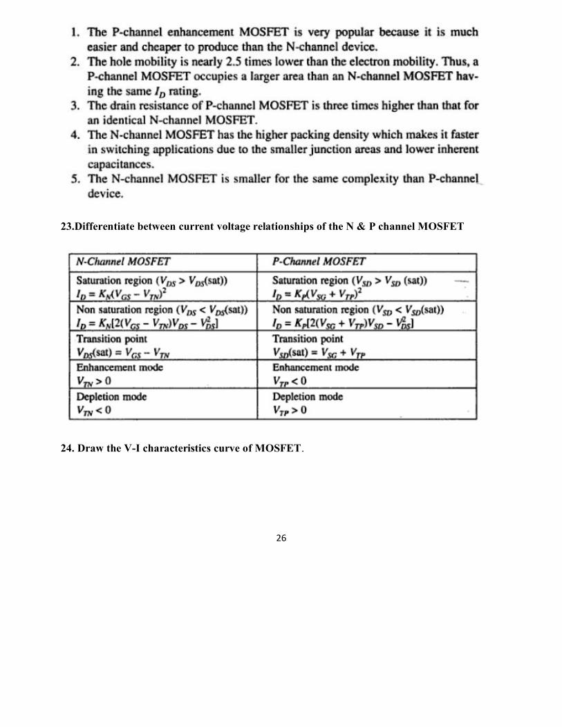
26
23.Differentiate between current voltage relationships of the N & P channel MOSFET
24. Draw the V-I characteristics curve of MOSFET.

27
PART B 1.Explain the operation of JFET and derive the drain and transfer characteristics. (16) Pg no : 3.1- 3.4 ( May 2015 & 2014,Nov 2014, 2012 & 2010, June 2013, 2012 & 2011) 2.With neat diagram explain the operation of MOSFET in Depletion mode and derive its current equations (16)
Pg no : 3.14- 3.21 ( Nov 2013 & 2010, June 2013) 3.With neat diagram explain the operation of MOSFET in Enhancement mode and derive its current equations (16)
Pg no : 3.13 & 3.14 ( May 2015 & 2014, Nov 2014 & 2011 )
4.Give some comparison of MOSFET. (8) Pg no : 3.21 (May 2014 & 2012)
5. Explain the operation of dual gate MOSFET (8)
Pg no : 3.33- 3.36 ( May 2015 & 2014)
6. Write expression of saturation drain current (10)
Pg no : 3.7 & 3.8 ( May 2015)

28
UNIT IV SPECIAL SEMICONDUCTOR DEVICES
PART A
1. What is a metal semiconductor contact?
A metal semiconductor contact is a contact between a metal and a semiconductor which according to the doping level and requirement may act as a rectifying diode or just a simple contact between a semiconductor device and the outside world.
2. Define contact potential in metal semiconductor contact.
The difference of potential between the work function of metal and the work function of semiconductor in a metal semiconductor contact is termed as contact potential.
3. Give the symbol and structure of schottky diode.
4. Give the applications of schottky diode.
1. It can switch off faster than bipolar diodes
2. It is used to rectify very high frequency signals (>10 MHZ)
3. as a switching device in digital computers.
4. It is used in clipping and clamping circuits.
5. It is used in communication systems such as frequency mixers, modulators and detectors.
5. Compare between PN and Schottky diodes

29
PN junction diode Schottky diode 1. Here the contact is established between two
Semiconductors
1. Here the contact is established between the
semiconductor and metal 2. current conduction is due to both
majority and minority carriers
2. current conduction is only due to
majority carriers 3. large reverse recovery time 3. Small reverse recovery time 4. barrier potential is high about 0.7 V 4. Barrier potential is low about 0.25 V 5. switching speed is less 5. switching speed is high 6. cannot operate at high frequency 6. can operate at very high frequency (>
300MHz) 6. Why zener diode is often preferred than PN diode.
When the reverse voltage reaches breakdown voltage in normal PN junction diode the current through the junction and the power dissipated at the junction will high. Such an operation is destructive and the diode gets damaged.
Whereas diode can be designed with adequate power dissipation capabilities to operate in
breakdown region. That diode is known as zener diode. It is heavily doped than ordinary diode. 7. Draw the V-I characteristics curve for zener diode.
8. What is zener breakdown?
Zener break down takes place when both sides of the junction are very heavily doped and

30
consequently the depletion layer is thin and consequently the depletion layer is tin. When a small value of reverse bias voltage is applied, a very strong electric field is set up across the thin depletion layer. This electric field is enough to break the covalent bonds. Now extremely large number of free charge carriers are produced which constitute the zener current. This process is known as zener break down.
9. What is avalanche break down?
When bias is applied, thermally generated carriers which are already present in the diode acquire sufficient energy from the applied potential to produce new carriers by removing valence electron from their bonds. These newly generated additional carriers acquire more energy from the potential and they strike the lattice and create more number of free electrons and holes. This process goes on as long as bias is increased and the number of free carriers gets multiplied. This process is termed as avalanche multiplication. Thus the break down which occurs in the junction resulting in heavy flow of current is termed as avalanche break down.
10. What is tunneling phenomenon?
The phenomenon of penetration of the charge carriers directly though the potential barrier instead of climbing over it is called as tunneling.
11. Give the application of tunnel diode.
As logic memory storage device
As microwave oscillator
In relaxation oscillator circuit
As an amplifier
As an ultra-high speed switch 12. Give the advantages and disadvantages of tunnel diode
Advantages
Low noise
Ease of operation
High speed
Low power
Disadvantages

31
Voltage range over which it can be operated is 1 V less.
Being a two terminal device there is no isolation between the input and output circuit. 13. Draw equivalent circuit of tunnel diode
• This is the equivalent circuit of tunnel diode when biased in negative resistance region.
• At higher frequencies the series R and L can be ignored.
• Hence equivalent circuit can be reduced to parallel combination of junction capacitance and negative resistance.
14. What is varactor diode? A varactor diode is best explained as a variable capacitor. Think of the depletion region as a variable dielectric. The diode is placed in reverse bias. The dielectric is “adjusted” by reverse bias voltage changes.
•Junction capacitance is present in all reverse biased diodes because of the depletion region. •Junction capacitance is optimized in a varactor diode and is used for high frequencies and switching applications. •Varactor diodes are often used for electronic tuning applications in FM radios and televisions. 15. What are the differences between a tunnel diode & an ordinary PN junction diode? Unlike an ordinary PN junction diode, the tunnel diode is heavily doped which esults in a very thin depletion region in terms of few Angstrom. The high electric field between the P & N regions causes tunneling of charge carriers resulting in a current flow with a very small bias voltage. Further , the tunnel diode exhibits negative resistance characteristics wherein the conduction current decreases with increase in the applied voltage.
16.Explain the advantages of tunnel diode? environmental immunity. Low cost Simplicity Low noise

32
High speed Low power consumption
17.Explain the disadvantages of tunnel diode?
Only disadvantage of tunnel diode are its low output voltage swing and it is a two terminal device . hence there is no isolation between input and output . hence transistor is used along with a tunnel diode for frequencies below 1 GHz.
18.Explain the applications of tunnel diode? . As a high speed switch .
(ii). in pulse and digital circuits .
(iii). in negative resistance and high frequency (micro wave ) oscillator .
(iv) in switch networks
(v).in timing and computer logic circuitry .
(vi). design of pulse generators and amplifiers
19. Explain the Advantages of photodiode?
a. can be used as variable resistance device.
b. Highly sensitive to the light.
c. The speed of the operation is very high . the switching of current and hence the resistance value from high to low or other wise is very fast .
20.Explain the Disadvantages of photodiode? a. The dark current is temperature dependent .
b. The overall photo diode characteristics are temperature dependent Hence have poor temperature stability
c. The current and change in current is in the range of TA which may not be sufficient to drive other circuits. Hence amplification is necessary

33
21.What is Pin diode ?
Pin diode is a high speed switching device, because its highly improved switching time in comparison with a PN diode.Inthis diode high resistivity intrinsic layer is sandwiched
between the heavily doped P and N regions thus it is named as PIN diode.
22.What is a varactor diode ?
The varactor diode is a semiconductor, voltage dependent variable capacitor diode. This special diode which is made for the application utilization of voltage variable properly hence it is called varactor diode or Varicaps (or) voltage cap.It is operated under reverse biased conditions so as to yield a variable junction capacitance.
23. What is the significance of varactor diode ?
The varactor diode is a semiconductor ,voltage deprndent ,variable capacitors diode.Their mode of operation depends on the capacitance that exists at the PN junction when it is reverse biased.
24.Why germanium instead of silicon is used for construction of SCR?
For the construction of SCR germanium is preferred than silicon because ,more silicon per ampere current is required. Hence the current rating is increased ,it require more silicon.
25.What are the methods used to turn on SCR ?
σ Voltage trigerring σ dV / dt trigerring
σ Gate trigerring
26.What is SCR ?
A Silicon Controlled Rectifier (SCR )is a three terminal ,three junction semiconductor device .It is unidirectional device. It converts alternating current into direct current and control the amount of power fed to the load .

34
27.Write an two different characteristics of SCR ? Forward characteristics Reverse characteristics
28.Mention the application of SCR.
σ It can be used as a speed control element in DC and Ac motors. (ii)It can be used as an inverter.
It can be used as an Converter.
29.Define breakdown voltage of SCR.
It can be defined as the minimum forward voltage at which the SCR starts conducting heavily.
30.Define latching current.
It can be defined as the maximum anode current that an SCr capable of passing without destruction.
31. Define holding current of an SCR .
It can be defined as the minimum value of anode current required to keep the SCR in ON position.
32.What is DIAC ?
Diac is a two terminal ,bi-directional semiconductor switching depending upon the polarity of the voltage applied across its main terminals .In operation ,diac is equivalent to two 4 layer diodes connected in antiparallel.
33.List out the applications of DIAC.
(i) It is used as a trigger device in TRIAC power control systems. (ii) It is used in lamp dimmer circuits (iii) It is used in heater control circuits (iv) It is used for speed control of universal motor.

35
34.A triac is considered as two SCRs connected in reverse parallel.Why?
The TRIAC is a bidirectional device.,i.e it conducts in both direction ,In order to achieve this characteristics two SCRs are connected in reverse and parallel.
35.Compare SCR with TRIAC.
SCR TRIAC
It is a unidirectional device It is a bidirectional device
It is triggered by a narrow positive pulse It is triggered by a narrow pulse of the
applied at the gate either polarity to the gate.
SCR are available only with large current Triac are available for both lower current
rating. and large current rating.
It has fast turn off The turn off time is less than SCR
UJT is used for triggering Diac is used for triggering
Applications: Phase control, Protection of Applications: Phase control, light dimmer
power suppliers
36.What is TRIAC ?
TRIAC is a three terminal bi-directional semiconductor switching device. It can conduct

36
in both the directions for any desired period.In operation it is equivalent to two SCRs connected in antiparallel .
36.Give the applications of UJT.
(i) It is used in timing circuits (ii)It is used in switching circuits. (iii) It is used in phase control circuits.
(iv) It is used in saw –tooth generators. (v)It is used in pulse generation.
38.Define dark current of a photo diode .
When there is no light ,the reverse biased photodiode carriers a current which is very small and is called as dark current.
39.What is photodiode ?
It is a light sensitive device used to convert light signal into electrical signal.
40.What is mean by solar cell ?
A solar cell is basically a PN junction diode which converts solar energy into electric energy.it is also called a solar energy converter.
41.What is Photo voltaic effect?
When the light is incident on the photodiode ,an internal voltage is generated,it causes the current flow through internal circuit even though no external source is applied.this generated emf is proportional to the frequency and the intensity of the incident light.This phenomenon is called photo voltaic effect.
42.What is known as photo conductive effect?
This is the absorption of incident light by an semiconductor resulting in increase in conductivity.
43. What is an LCD ?
LCD is a passive type display devices used for display of numeric and alphanumeric character in dotmatrix and seven segment display.The main advantage of LCDis the low power consumption because no light generation is required .
44.On what factor does the color of the light emitted by a LED depend ?

37
(i) Energy gap of the material (ii) The colour of the emitted light depends on the type of the material used.
45. Explain the Advantages of LED ? The various advantages of LED are .
(i) LED are small in size , and hence can be regarded as point source of light . because of their small size , several thousand of LEDs can be packed in one sq .metre area
(ii)The brightness of light emitted by LED depends on the current flowing through LED.hence the brightness of light can be smoothly controlled by varying the current. This makes possible to operate LED displays under different ambient lighting conditions .
46.Explain the Disadvantages of LED ?
a. It draws considerable current requiring frequent replacement of battery in low power battery operated devices.
b. Luminous efficiency of LEDs is low which is about 1.5 lumen/watt. c. The characteristics are affected by temperature d. Need large power for the operation compared to normal p-n junction.
47.Write an application of LED?
e. All kind of visual display. In seven segment displays and alpha numeric displays. Such displays are commonly used in watches and calculators.
f. In the optical devices such as optocouplers . g. As ON-OFF indicator in various types of electronic circuits. h. LEDs useful in remote controls.
48.Different types of LCD ?
1. Dynamic scattering LCD 2. Field effect LCD

38
PART B
1.Explain about metal semiconductor junction (12) Pg no : 4.1 – 4.6 ( May 2015) 2.Explain the operation of zener diode and how it is used as a voltage regulator. (16) Pg no : 4.16 – 4.20 ( Nov 2014 & May 2014) 3.Explain the operation of tunnel diode and draw its equivalent circuit. (12) Pg no : 4.26 – 4.29 ( May 2015 & 2013, Nov 2013 & 2010, June 2010) 4.With neat diagram give the working principle of LASER diode (8)
Pg no : 429 ( May 2014 & Nov 2011)
5. Explain the operation of Schottky barrier diode (8)
Pg no : 4.14 – 4.16 ( May 2014)
6.With neat diagram explain about varactor diode. (8)
Pg no : 4.25 ( May 2015,2014 & 2013, Nov 2014) 17. With neat diagram give the working principle of LDR (8) Pg no : 4.30 & 4.31 ( Nov 2013, 2012, 2011 , May 2012 & June 2011)

39
UNIT V POWER DEVICES AND DISPLAY DEVICES
PART A
1. What is intrinsic stand- off ratio of an UJT?
If a voltage VBB is applied between the bases with emitter open the circuit will behave as a potential
divider. Thus the voltage VBB will be divided across RB1 and RB2
Voltage across resistance RB1,
The resistance ratio ƞ = RB1 / RBB is known as intrinsic stand -off ratio
2. Give the VI characteristics of UJT
3. Mention the applications of UJT.
1. It is used in timing circuits
2. It is used in switching circuits
3. It is used in phase control circuits
4. It can be used as trigger device for SCR and triac.
5. It is used in saw tooth generator.
6. It is used for pulse generation
40
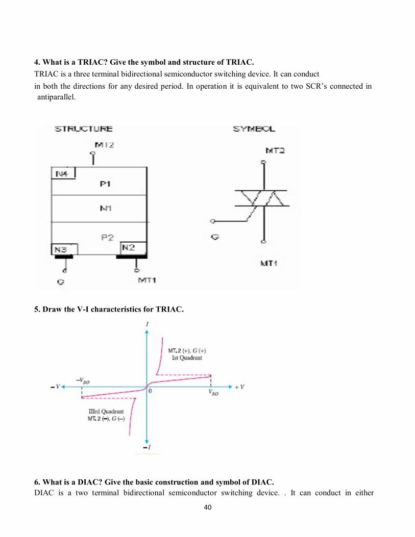
4. What is a TRIAC? Give the symbol and structure of TRIAC.
TRIAC is a three terminal bidirectional semiconductor switching device. It can conduct
in both the directions for any desired period. In operation it is equivalent to two SCR’s connected in antiparallel.
5. Draw the V-I characteristics for TRIAC.
6. What is a DIAC? Give the basic construction and symbol of DIAC. DIAC is a two terminal bidirectional semiconductor switching device. . It can conduct in either

41
direction depending upon the polarity of the voltage applied across its main terminals. In operation DIAC is equivalent to two 4 layer diodes connected in antiparallel.
7. Give the application of TRIAC.
1. Heater control
2. Motor speed control
3. Phase control
4. Static switches
8. Draw the V-I curve for DIAC
9. Give some applications of DIAC.
1. To trigger TRIAC
2. Motor speed control
3. Heat control
4. Light dimmer circuits
42
10. Why SCR cannot be used as a bidirectional switch.
SCR can do conduction only when anode is positive with respect to cathode with proper gate current. Therefore, SCR operates only in one direction and cannot be used as bidirectional switch.
11. How turning on of SCR is done?
1. By increasing the voltage across SCR above forward break over voltage.
2. By applying a small positive voltage at gate.
3. By rapidly increasing the anode to cathode voltage.
4. By irradiating SCR with light. 12. How turning off of SCR is done?
1. By reversing the polarity of anode to cathode voltage.
2. By reducing the current through the SCR below holding current.
3. By interrupting anode current by means of momentarily series or parallel switching 13. Define holding current in a SCR.
Holding current is defined as the minimum value of anode current to keep the SCR ON. 14. List the advantages of SCR.
1. SCR can handle and control large currents.
2. Its switching speed is very high
3. It has no moving parts, therefore it gives noiseless operation.
4. Its operating efficiency is high. 15. List the application of SCR.
1. It can be used as a speed controller in DC and AC motors.
2. It can be used as an inverter.
3. It can be used as a converter
4. It is used in battery chargers.
5. It is used for phase control and heater control.
6. It is used in light dimming control circuits
16. Compare SCR with TRIAC

43
17. Differentiate BJT and UJT
.
18. State the principle of operation of an LED
When a free electron from the higher energy level gets recombined with the hole, it gives the light output. Here in case of LEDs, the supply of higher level electrons is provided by the battery connection.
19. Give the advantages of LED
20. State some disadvantages of LED
21. List the applications of LED

44
22. Give some advantages and disadvantages for LCD Advantages of LCD Low power is required
Good contrast
Low cost
Disadvantages of LCD
Speed of operation is slow
LCD occupy a large area
LCD life span is quite small, when used on d.c. Therefore, they are used with a.c. suppliers.
23. Give applications of LCD Used as numerical counters for counting production items.
Analog quantities can also be displayed as a number on a suitable device. (e.g.) Digital multimeter.
Used for solid state video displays.
Used for image sensing circuits.
Used for numerical display in pocket calculators.
24. Compare LEDs and LCDs.
25. Give some notes on CCD. A charge-coupled device (CCD) is a device for the movement of electrical charge, usually from within the device to an area where the charge can be manipulated, for example conversion into a digital value. This is achieved by "shifting" the signals between stages within the device one at a time. CCDs move charge between capacitive bins in the device, with the shift allowing for the transfer of charge between bins. The CCD is a major piece of technology in digital imaging. In a CCD image sensor,
45
pixels are represented by p-doped MOS capacitors.
PART B 1. Explain the construction, operation, V-I characteristics and application of SCR and explain its two transistor model. (16)
Pg no : 5.6 – 5.8 (Nov 2013 & 2011, May 2014 & June 2011) 2.Explain the construction, operation, equivalent circuit V-I characteristics and application of UJT (16)
Pg no : 5.1 – 5.4 (Nov 2014, 2013, 2012, May 2014, 2013, 2012 & June 2010) 3.Explain the construction, operation, equivalent circuit V-I characteristics and application of TRIAC (16)
Pg no : 5.15 & 5.16 (Nov 2011 & 2010) 4.Explain the construction, operation, equivalent circuit V-I characteristics and application of DIAC (16)
Pg no : 5.16 & 5.17 (Nov 2012 & 2010, May 2012) 5.Explain : ( a) DMOS (8) Pg no : 5.23 & 5.24 (b) VMOS (8) Pg no : 5.24 & 5.25 6.Explain the operation of Photo transistor & Photodiode (8) Pg no : 5.32 – 5.35 ( Nov 2014,2011,2010, May 2014 & 2013) 7.With neat diagram explain the operation of Solar cell. (8). Pg no : 5.38 & 5.39 (May 2014) 8.Explain: (a) Power BJT (8) Pg no : 5.18 – 5.22 (May 2015) (b) Power MOSFET (8) Pg no : 5.22 & 5.23 (May 2015) 9.Explain the operation of Charge coupled device (8) Pg no : 5.39 – 5.41 (May 2015 & 2014 , Nov 2014)