Electronic Devices & Circuit Theory (Course Code Here)
84
Electronic Devices & Circuit Theory (Course Code Here) Department of Computer Engineering Khwaja Fareed University of Engineering and Information Technology Rahim Yar Khan, Pakistan Draft Copy – 1 August 2017
-
Upload
khangminh22 -
Category
Documents
-
view
0 -
download
0
Transcript of Electronic Devices & Circuit Theory (Course Code Here)

Electronic Devices & Circuit Theory(Course Code Here)
Department of Computer Engineering
Khwaja Fareed University of Engineering andInformation Technology
Rahim Yar Khan, Pakistan
Draft Copy – 1 August 2017

ii Contents
Draft Copy – 1 August 2017

Contents
1 Lab 1: I-V Characteristics of a Diode 11.1 Objectives: . . . . . . . . . . . . . . . . . . . . . . . . . . . . . . . . . . . . 11.2 Parts and Equipment: . . . . . . . . . . . . . . . . . . . . . . . . . . . . . 11.3 Circuit Diagram: . . . . . . . . . . . . . . . . . . . . . . . . . . . . . . . . 1
1.3.1 Pin Diagram . . . . . . . . . . . . . . . . . . . . . . . . . . . . . . . 21.4 Procedure: . . . . . . . . . . . . . . . . . . . . . . . . . . . . . . . . . . . . 21.5 Observations and Calculations: . . . . . . . . . . . . . . . . . . . . . . . . 21.6 I-V Characteristics: . . . . . . . . . . . . . . . . . . . . . . . . . . . . . . . 31.7 Precautions: . . . . . . . . . . . . . . . . . . . . . . . . . . . . . . . . . . . 31.8 Course Learning Outcomes . . . . . . . . . . . . . . . . . . . . . . . . . . 41.9 Review Questions: . . . . . . . . . . . . . . . . . . . . . . . . . . . . . . . 4
2 Lab 2: Diode as Clipper 72.1 Objective: . . . . . . . . . . . . . . . . . . . . . . . . . . . . . . . . . . . . . 72.2 Parts and Equipment: . . . . . . . . . . . . . . . . . . . . . . . . . . . . . 72.3 Circuit Diagram: . . . . . . . . . . . . . . . . . . . . . . . . . . . . . . . . 72.4 Procedure: . . . . . . . . . . . . . . . . . . . . . . . . . . . . . . . . . . . . 82.5 Precautions: . . . . . . . . . . . . . . . . . . . . . . . . . . . . . . . . . . . 92.6 Course Learning Outcomes . . . . . . . . . . . . . . . . . . . . . . . . . . 92.7 Review Questions: . . . . . . . . . . . . . . . . . . . . . . . . . . . . . . . 9
3 Lab 3: Diode as Clamper 133.1 Objective: . . . . . . . . . . . . . . . . . . . . . . . . . . . . . . . . . . . . . 133.2 Parts and Equipment: . . . . . . . . . . . . . . . . . . . . . . . . . . . . . 133.3 Circuit Diagram: . . . . . . . . . . . . . . . . . . . . . . . . . . . . . . . . 133.4 Procedure: . . . . . . . . . . . . . . . . . . . . . . . . . . . . . . . . . . . . 133.5 Precautions: . . . . . . . . . . . . . . . . . . . . . . . . . . . . . . . . . . . 143.6 Course Learning Outcomes . . . . . . . . . . . . . . . . . . . . . . . . . . 153.7 Review Questions: . . . . . . . . . . . . . . . . . . . . . . . . . . . . . . . 15
4 Lab 4: Diode as Half Rectifier 194.1 Objective: . . . . . . . . . . . . . . . . . . . . . . . . . . . . . . . . . . . . . 194.2 Parts and Equipment: . . . . . . . . . . . . . . . . . . . . . . . . . . . . . 194.3 Circuit Diagram: . . . . . . . . . . . . . . . . . . . . . . . . . . . . . . . . 194.4 Procedure: . . . . . . . . . . . . . . . . . . . . . . . . . . . . . . . . . . . . 194.5 Efficiency: . . . . . . . . . . . . . . . . . . . . . . . . . . . . . . . . . . . . 204.6 Precautions: . . . . . . . . . . . . . . . . . . . . . . . . . . . . . . . . . . . 21
iii
Draft Copy – 1 August 2017

iv Contents
4.7 Course Learning Outcomes . . . . . . . . . . . . . . . . . . . . . . . . . . 214.8 Review Questions: . . . . . . . . . . . . . . . . . . . . . . . . . . . . . . . 21
5 Lab 5: Diode as Full Wave Rectifier 255.1 Objective: . . . . . . . . . . . . . . . . . . . . . . . . . . . . . . . . . . . . . 255.2 Parts and Equipment: . . . . . . . . . . . . . . . . . . . . . . . . . . . . . 255.3 Circuit Diagram: . . . . . . . . . . . . . . . . . . . . . . . . . . . . . . . . 255.4 Procedure: . . . . . . . . . . . . . . . . . . . . . . . . . . . . . . . . . . . . 255.5 Efficiency: . . . . . . . . . . . . . . . . . . . . . . . . . . . . . . . . . . . . 265.6 Precautions: . . . . . . . . . . . . . . . . . . . . . . . . . . . . . . . . . . . 275.7 Course Learning Outcomes . . . . . . . . . . . . . . . . . . . . . . . . . . 275.8 Review Questions: . . . . . . . . . . . . . . . . . . . . . . . . . . . . . . . 27
6 Lab 6: Diode as Full Wave Bridge Rectifier 316.1 Objective: . . . . . . . . . . . . . . . . . . . . . . . . . . . . . . . . . . . . . 316.2 Parts and Equipment: . . . . . . . . . . . . . . . . . . . . . . . . . . . . . 316.3 Circuit Diagram: . . . . . . . . . . . . . . . . . . . . . . . . . . . . . . . . 316.4 Procedure: . . . . . . . . . . . . . . . . . . . . . . . . . . . . . . . . . . . . 316.5 Efficiency: . . . . . . . . . . . . . . . . . . . . . . . . . . . . . . . . . . . . 326.6 Precautions: . . . . . . . . . . . . . . . . . . . . . . . . . . . . . . . . . . . 336.7 Course Learning Outcomes . . . . . . . . . . . . . . . . . . . . . . . . . . 336.8 Review Questions: . . . . . . . . . . . . . . . . . . . . . . . . . . . . . . . 33
7 Lab 7: Diode in Voltage Multiplier 377.1 Objective: . . . . . . . . . . . . . . . . . . . . . . . . . . . . . . . . . . . . . 377.2 Parts and Equipment: . . . . . . . . . . . . . . . . . . . . . . . . . . . . . 377.3 Circuit Diagram: . . . . . . . . . . . . . . . . . . . . . . . . . . . . . . . . 377.4 Procedure: . . . . . . . . . . . . . . . . . . . . . . . . . . . . . . . . . . . . 377.5 Precautions: . . . . . . . . . . . . . . . . . . . . . . . . . . . . . . . . . . . 387.6 Course Learning Outcomes . . . . . . . . . . . . . . . . . . . . . . . . . . 387.7 Review Questions: . . . . . . . . . . . . . . . . . . . . . . . . . . . . . . . 38
8 Lab 8: Zener Diode 418.1 Objective: . . . . . . . . . . . . . . . . . . . . . . . . . . . . . . . . . . . . . 418.2 Equipment and Components: . . . . . . . . . . . . . . . . . . . . . . . . . 418.3 Circuit Diagram: . . . . . . . . . . . . . . . . . . . . . . . . . . . . . . . . 418.4 Procedure: . . . . . . . . . . . . . . . . . . . . . . . . . . . . . . . . . . . . 428.5 Precautions: . . . . . . . . . . . . . . . . . . . . . . . . . . . . . . . . . . . 438.6 Course Learning Outcomes . . . . . . . . . . . . . . . . . . . . . . . . . . 438.7 Review Questions: . . . . . . . . . . . . . . . . . . . . . . . . . . . . . . . 43
9 Lab 9: Common Emitter Characteristics of BJT 479.1 Objective: . . . . . . . . . . . . . . . . . . . . . . . . . . . . . . . . . . . . . 479.2 Equipment and Components: . . . . . . . . . . . . . . . . . . . . . . . . . 479.3 Circuit Diagram: . . . . . . . . . . . . . . . . . . . . . . . . . . . . . . . . 47
Draft Copy – 1 August 2017

Contents v
9.4 Procedure: . . . . . . . . . . . . . . . . . . . . . . . . . . . . . . . . . . . . 479.5 Input Characteristics: . . . . . . . . . . . . . . . . . . . . . . . . . . . . . . 499.6 Output Characteristics: . . . . . . . . . . . . . . . . . . . . . . . . . . . . . 499.7 Precautions: . . . . . . . . . . . . . . . . . . . . . . . . . . . . . . . . . . . 499.8 Course Learning Outcomes . . . . . . . . . . . . . . . . . . . . . . . . . . 509.9 Review Questions: . . . . . . . . . . . . . . . . . . . . . . . . . . . . . . . 50
10 Lab 10: Common Base Characteristics of BJT 5310.1 Objective: . . . . . . . . . . . . . . . . . . . . . . . . . . . . . . . . . . . . . 5310.2 Equipment and Components: . . . . . . . . . . . . . . . . . . . . . . . . . 5310.3 Circuit Diagram: . . . . . . . . . . . . . . . . . . . . . . . . . . . . . . . . 5310.4 Procedure: . . . . . . . . . . . . . . . . . . . . . . . . . . . . . . . . . . . . 5310.5 Input Characteristics: . . . . . . . . . . . . . . . . . . . . . . . . . . . . . . 5410.6 Output Characteristics . . . . . . . . . . . . . . . . . . . . . . . . . . . . . 5610.7 Precautions: . . . . . . . . . . . . . . . . . . . . . . . . . . . . . . . . . . . 5610.8 Course Learning Outcomes . . . . . . . . . . . . . . . . . . . . . . . . . . 5710.9 Review Questions: . . . . . . . . . . . . . . . . . . . . . . . . . . . . . . . 57
11 Lab 11: Common Collector Characteristics of BJT 6111.1 Objective: . . . . . . . . . . . . . . . . . . . . . . . . . . . . . . . . . . . . . 6111.2 Equipment and Components: . . . . . . . . . . . . . . . . . . . . . . . . . 6111.3 Circuit Diagram: . . . . . . . . . . . . . . . . . . . . . . . . . . . . . . . . 6111.4 Procedure: . . . . . . . . . . . . . . . . . . . . . . . . . . . . . . . . . . . . 6111.5 Input Characteristics: . . . . . . . . . . . . . . . . . . . . . . . . . . . . . . 6211.6 Output Characteristics . . . . . . . . . . . . . . . . . . . . . . . . . . . . . 6311.7 Precautions: . . . . . . . . . . . . . . . . . . . . . . . . . . . . . . . . . . . 6311.8 Course Learning Outcomes . . . . . . . . . . . . . . . . . . . . . . . . . . 6311.9 Review Questions: . . . . . . . . . . . . . . . . . . . . . . . . . . . . . . . 63
12 Lab 12: Metal Oxide Semiconductor Field Effect Transistor 6712.1 Objective: . . . . . . . . . . . . . . . . . . . . . . . . . . . . . . . . . . . . . 6712.2 Equipment and Components: . . . . . . . . . . . . . . . . . . . . . . . . . 6712.3 Circuit Diagram: . . . . . . . . . . . . . . . . . . . . . . . . . . . . . . . . 6712.4 Procedure: . . . . . . . . . . . . . . . . . . . . . . . . . . . . . . . . . . . . 6712.5 Transfer Characteristics: . . . . . . . . . . . . . . . . . . . . . . . . . . . . 6912.6 Course Learning Outcomes . . . . . . . . . . . . . . . . . . . . . . . . . . 6912.7 Review Questions: . . . . . . . . . . . . . . . . . . . . . . . . . . . . . . . 69
13 Lab 12: Junction Field Effect Transistor 7313.1 Objective: . . . . . . . . . . . . . . . . . . . . . . . . . . . . . . . . . . . . . 7313.2 Equipment and Components: . . . . . . . . . . . . . . . . . . . . . . . . . 7313.3 Circuit Diagram: . . . . . . . . . . . . . . . . . . . . . . . . . . . . . . . . 7313.4 Procedure: . . . . . . . . . . . . . . . . . . . . . . . . . . . . . . . . . . . . 7313.5 Transfer Characteristics: . . . . . . . . . . . . . . . . . . . . . . . . . . . . 7513.6 Course Learning Outcomes . . . . . . . . . . . . . . . . . . . . . . . . . . 75
Draft Copy – 1 August 2017

vi Contents
13.7 Review Questions: . . . . . . . . . . . . . . . . . . . . . . . . . . . . . . . 75
Draft Copy – 1 August 2017

Chapter 1
Lab 1: I-V Characteristics of aDiode
1.1 Objectives:
To study VI Characteristics of a PN Junction diode
1.2 Parts and Equipment:
• Digital and analog Multimeter
• Power Supply
• Bread board
• Connecting wires
• Diode IN4007
• Resistors 1K, 470K
1.3 Circuit Diagram:
• To get familiar with the usage of the available lab equipment.
• To get familiar with Prototyping board (breadboard)
• To describe and verify the operation for the AND, OR, NOT, NAND, NOR,XOR, XNOR gates.
• To study the representation of these functions by truth tables, logic diagramsand Boolean algebra
• To Introduce a basic knowledge in integrated circuit devices operation itemTo practice how to build a simple digital circuit using ICs and other digitalcomponents .
• Learn how to Wire a circuit
1
Draft Copy – 1 August 2017

2 Lab 1: I-V Characteristics of a Diode
1.3.1 Pin Diagram
Figure 1.1: Diodes connected in series with DC voltage source.
1.4 Procedure:
• Connect the circuit on the bread board as shown in the diagram.
• Gradually vary DC supply and measure the voltage drop across the diode andacross resistor using digital voltmeter.
• Record the values in the table.
• Plot the graph between Id(yaxis) and Vd(xaxis)
– based upon the values obtained in the table
– based upon the diode equation
• Now reverse the diode and replace 1K resistor with 470K resistor and repeatthe previous steps for this circuit as well
1.5 Observations and Calculations:
Draft Copy – 1 August 2017

§1.6 I-V Characteristics: 3
Figure 1.2: Calculations
1.6 I-V Characteristics:
1.7 Precautions:
• All the connections should be neat and tight
• Multimeter should be checked before performing the experiment
• Resistors and diode should be checked
• Voltage should not be increased to much higher value lest it cause damages tothe circuit
Draft Copy – 1 August 2017

4 Lab 1: I-V Characteristics of a Diode
Figure 1.3: I-V Characteristics
1.8 Course Learning Outcomes
1.9 Review Questions:
1. On what part of the curve is forward biased diode normally operated?
2. What happens to the barrier potential when the temperature increases?
3. What is the simplest way to visualize a diode?
Draft Copy – 1 August 2017

§1.9 Review Questions: 5
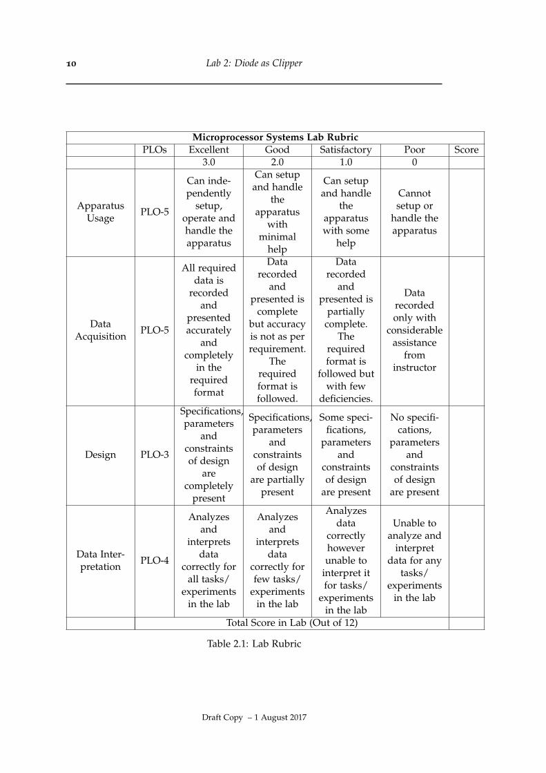
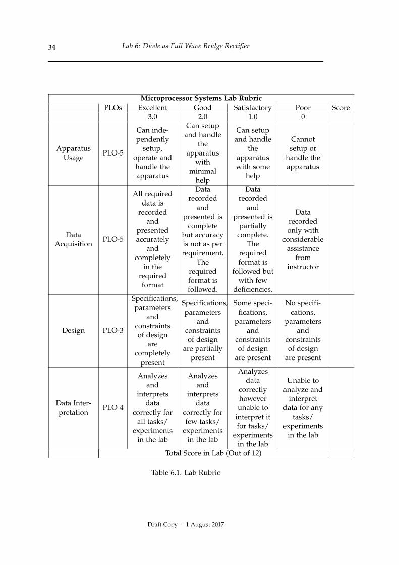
Microprocessor Systems Lab RubricPLOs Excellent Good Satisfactory Poor Score
3.0 2.0 1.0 0
ApparatusUsage
PLO-5
Can inde-pendently
setup,operate andhandle theapparatus
Can setupand handle
theapparatus
withminimal
help
Can setupand handle
theapparatuswith some
help
Cannotsetup or
handle theapparatus
DataAcquisition
PLO-5
All requireddata is
recordedand
presentedaccurately
andcompletely
in therequiredformat
Datarecorded
andpresented is
completebut accuracyis not as perrequirement.
Therequiredformat isfollowed.
Datarecorded
andpresented is
partiallycomplete.
Therequiredformat is
followed butwith few
deficiencies.
Datarecordedonly with
considerableassistance
frominstructor
Design PLO-3
Specifications,parameters
andconstraintsof design
arecompletely
present
Specifications,parameters
andconstraintsof design
are partiallypresent
Some speci-fications,
parametersand
constraintsof design
are present
No specifi-cations,
parametersand
constraintsof design
are present
Data Inter-pretation
PLO-4
Analyzesand
interpretsdata
correctly forall tasks/
experimentsin the lab
Analyzesand
interpretsdata
correctly forfew tasks/
experimentsin the lab
Analyzesdata
correctlyhoweverunable to
interpret itfor tasks/
experimentsin the lab
Unable toanalyze and
interpretdata for any
tasks/experiments
in the lab
Total Score in Lab (Out of 12)
Table 1.1: Lab Rubric
Draft Copy – 1 August 2017

6 Lab 1: I-V Characteristics of a Diode
4. Under what condition is the diode never intentionally operated?
Draft Copy – 1 August 2017

Chapter 2
Lab 2: Diode as Clipper
2.1 Objective:
To study diodeâAZs clipping function
2.2 Parts and Equipment:
• Oscilloscope
• 1N4007 diode
• Digital Multimeter
• Connecting wires
• Bread board
• Signal Generator
• Resistor 10 KΩ
2.3 Circuit Diagram:
Figure 2.1: Diode as Clipper
7
Draft Copy – 1 August 2017

8 Lab 2: Diode as Clipper
2.4 Procedure:
• Set the signal generator to 5V peak, 1KHz Sin wave
• Observe the input and output waveforms of the circuit with the help of anoscilloscope
Figure 2.2: Input and Output waveform plot
• Reverse the diode and observe the waveform
Figure 2.3: Diode as Clipper
• Connect the diode in following configuration
• Observe the output waveform after setting dc source to 3V
• Reverse the diode and observe the output waveform
• Reverse battery polarity and observe the waveform
• Reverse diode and observe the waveform
• Connect the circuit in following configuration
Draft Copy – 1 August 2017

§2.5 Precautions: 9
Figure 2.4: Diode as Clipper
Figure 2.5: Reversed battery polarities
2.5 Precautions:
• All the connections should be neat and tight
• Multimeter should be checked before performing the experiment
• Resistors and diode should be checked
• Voltage should not be increased to much higher value lest it cause damages tothe circuit
2.6 Course Learning Outcomes
2.7 Review Questions:
1. What is the function of Clipper circuit?
Draft Copy – 1 August 2017
10 Lab 2: Diode as Clipper
Microprocessor Systems Lab RubricPLOs Excellent Good Satisfactory Poor Score
3.0 2.0 1.0 0
ApparatusUsage
PLO-5
Can inde-pendently
setup,operate andhandle theapparatus
Can setupand handle
theapparatus
withminimal
help
Can setupand handle
theapparatuswith some
help
Cannotsetup or
handle theapparatus
DataAcquisition
PLO-5
All requireddata is
recordedand
presentedaccurately
andcompletely
in therequiredformat
Datarecorded
andpresented is
completebut accuracyis not as perrequirement.
Therequiredformat isfollowed.
Datarecorded
andpresented is
partiallycomplete.
Therequiredformat is
followed butwith few
deficiencies.
Datarecordedonly with
considerableassistance
frominstructor
Design PLO-3
Specifications,parameters
andconstraintsof design
arecompletely
present
Specifications,parameters
andconstraintsof design
are partiallypresent
Some speci-fications,
parametersand
constraintsof design
are present
No specifi-cations,
parametersand
constraintsof design
are present
Data Inter-pretation
PLO-4
Analyzesand
interpretsdata
correctly forall tasks/
experimentsin the lab
Analyzesand
interpretsdata
correctly forfew tasks/
experimentsin the lab
Analyzesdata
correctlyhoweverunable to
interpret itfor tasks/
experimentsin the lab
Unable toanalyze and
interpretdata for any
tasks/experiments
in the lab
Total Score in Lab (Out of 12)
Table 2.1: Lab Rubric
Draft Copy – 1 August 2017

§2.7 Review Questions: 11
Figure 2.6: Reversed Diode
Figure 2.7: Diode as Clipper
2. What characteristics of diode make it a useful clipper??
3. What is the difference between positive and negative clipper??
Draft Copy – 1 August 2017

12 Lab 2: Diode as Clipper
4. What is the effect of adding biased to the diode in a clipper circuit?
Draft Copy – 1 August 2017

Chapter 3
Lab 3: Diode as Clamper
3.1 Objective:
To study diodeâAZs clamping action
3.2 Parts and Equipment:
• Oscilloscope
• 1N4007 diode
• Digital Multimeter
• Transformer
• Connecting wires
• Bread board
• Signal Generator
• Resistor 10 KΩ
• Capacitor 0.1 µF
3.3 Circuit Diagram:
3.4 Procedure:
• Connect the circuit as shown in the diagram and draw input sine wave
• Set signal generator to 10 volts peak to peak sine wave position
• Observe the input and output waveforms of the circuit with the help of anoscilloscope
13
Draft Copy – 1 August 2017

14 Lab 3: Diode as Clamper
Figure 3.1: Diode as Clapper
Figure 3.2: Input and Output waveform plot
• Reverse the Diode and Observe the waveform
• Connect the diode in following configuration
• Observe the output waveform after setting dc source to 3V
• Reverse the diode and observe the output waveform
• Reverse battery polarity and observe the waveform
• Reverse the diode and observe the waveform
3.5 Precautions:
• All the connections should be neat and tight
• Multimeter should be checked before performing the experiment
• Resistors and diode should be checked
• Voltage should not be increased to much higher value lest it cause damages tothe circuit
Draft Copy – 1 August 2017

§3.6 Course Learning Outcomes 15
Figure 3.3: Diode coonected in reversed configuration
Figure 3.4: Diode as Clamper
3.6 Course Learning Outcomes
3.7 Review Questions:
1. What is the function of a clamper circuit?
2. What is the function of a capacitor and resistor in an unbiased clamper circuit?
Draft Copy – 1 August 2017

16 Lab 3: Diode as Clamper
Microprocessor Systems Lab RubricPLOs Excellent Good Satisfactory Poor Score
3.0 2.0 1.0 0
ApparatusUsage
PLO-5
Can inde-pendently
setup,operate andhandle theapparatus
Can setupand handle
theapparatus
withminimal
help
Can setupand handle
theapparatuswith some
help
Cannotsetup or
handle theapparatus
DataAcquisition
PLO-5
All requireddata is
recordedand
presentedaccurately
andcompletely
in therequiredformat
Datarecorded
andpresented is
completebut accuracyis not as perrequirement.
Therequiredformat isfollowed.
Datarecorded
andpresented is
partiallycomplete.
Therequiredformat is
followed butwith few
deficiencies.
Datarecordedonly with
considerableassistance
frominstructor
Design PLO-3
Specifications,parameters
andconstraintsof design
arecompletely
present
Specifications,parameters
andconstraintsof design
are partiallypresent
Some speci-fications,
parametersand
constraintsof design
are present
No specifi-cations,
parametersand
constraintsof design
are present
Data Inter-pretation
PLO-4
Analyzesand
interpretsdata
correctly forall tasks/
experimentsin the lab
Analyzesand
interpretsdata
correctly forfew tasks/
experimentsin the lab
Analyzesdata
correctlyhoweverunable to
interpret itfor tasks/
experimentsin the lab
Unable toanalyze and
interpretdata for any
tasks/experiments
in the lab
Total Score in Lab (Out of 12)
Table 3.1: Lab Rubric
Draft Copy – 1 August 2017
§3.7 Review Questions: 17
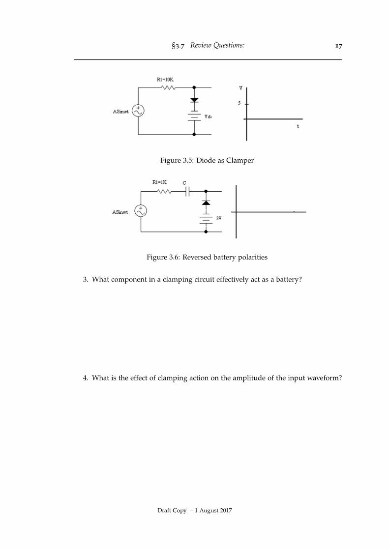
Figure 3.5: Diode as Clamper
Figure 3.6: Reversed battery polarities
3. What component in a clamping circuit effectively act as a battery?
4. What is the effect of clamping action on the amplitude of the input waveform?
Draft Copy – 1 August 2017

18 Lab 3: Diode as Clamper
Figure 3.7: Reversed Diode
Draft Copy – 1 August 2017

Chapter 4
Lab 4: Diode as Half Rectifier
4.1 Objective:
To demonstrate the use of a diode as a half wave rectifier
4.2 Parts and Equipment:
• Oscilloscope
• 1N4007 diode
• Digital Multimeter
• Transformer
• Connecting wires
• Bread board
• Signal Generator
• Resistor 10 KΩ
• Capacitor 0.1 µF
4.3 Circuit Diagram:
4.4 Procedure:
• Connect the circuit as shown in figure
• Measure the ac voltage across the output of the voltage transformer
• Observe the input and output waveforms of the circuit with the help of theoscilloscope
19
Draft Copy – 1 August 2017

20 Lab 4: Diode as Half Rectifier
Figure 4.1: Half wave Rectifier Circuit
Figure 4.2: Input and Output waveform plot
• Measure the average/dc value of output voltage with the help of voltmeter
• Calculate average/dc value using the formula and compare
Vdc =Vmax
π
• Connect oscilloscope across the diode and find the peak value of the sinusoidalwaveform. That will be the PIV of the rectifier
4.5 Efficiency:
• Find Vrms, Irms, Vdc and Idc to calculate the efficiency using the relation:
η = (Vdc)(Idc)(Vrms)(Irms)
• Now connect a 100 µF capacitor as shown and observe the output
Draft Copy – 1 August 2017

§4.6 Precautions: 21
Figure 4.3: Rectifier
• Find Vdc and ripple factor using the formula. Also find Vdc using voltmeter andcompare
Vdc =VPR
1+1/2 fr RLC
%r = 12√
3 fr RLC× 100
4.6 Precautions:
• All the connections should be neat and tight
• Multimeter should be checked before performing the experiment
• Resistors and diode should be checked
• Voltage should not be increased to much higher value lest it cause damages tothe circuit
4.7 Course Learning Outcomes
4.8 Review Questions:
1. What is called the process of changing an AC voltage to a pulsating DC voltage?
Draft Copy – 1 August 2017

22 Lab 4: Diode as Half Rectifier
Microprocessor Systems Lab RubricPLOs Excellent Good Satisfactory Poor Score
3.0 2.0 1.0 0
ApparatusUsage
PLO-5
Can inde-pendently
setup,operate andhandle theapparatus
Can setupand handle
theapparatus
withminimal
help
Can setupand handle
theapparatuswith some
help
Cannotsetup or
handle theapparatus
DataAcquisition
PLO-5
All requireddata is
recordedand
presentedaccurately
andcompletely
in therequiredformat
Datarecorded
andpresented is
completebut accuracyis not as perrequirement.
Therequiredformat isfollowed.
Datarecorded
andpresented is
partiallycomplete.
Therequiredformat is
followed butwith few
deficiencies.
Datarecordedonly with
considerableassistance
frominstructor
Design PLO-3
Specifications,parameters
andconstraintsof design
arecompletely
present
Specifications,parameters
andconstraintsof design
are partiallypresent
Some speci-fications,
parametersand
constraintsof design
are present
No specifi-cations,
parametersand
constraintsof design
are present
Data Inter-pretation
PLO-4
Analyzesand
interpretsdata
correctly forall tasks/
experimentsin the lab
Analyzesand
interpretsdata
correctly forfew tasks/
experimentsin the lab
Analyzesdata
correctlyhoweverunable to
interpret itfor tasks/
experimentsin the lab
Unable toanalyze and
interpretdata for any
tasks/experiments
in the lab
Total Score in Lab (Out of 12)
Table 4.1: Lab Rubric
Draft Copy – 1 August 2017

§4.8 Review Questions: 23
Figure 4.4: Diode as Half wave Rectifier
2. How often does current flow in a half wave rectifier with reference to AC input?
3. At what point on the input cycle does the PIV occur?
Draft Copy – 1 August 2017

24 Lab 4: Diode as Half Rectifier
Draft Copy – 1 August 2017
Chapter 5
Lab 5: Diode as Full Wave Rectifier
5.1 Objective:
To demonstrate the use of a diode as a Full wave rectifier
5.2 Parts and Equipment:
• Oscilloscope
• 1N4007 diode
• Digital Multimeter
• Transformer
• Connecting wires
• Bread board
• Signal Generator
• Resistor 10KΩ
• Capacitor 0.1µF
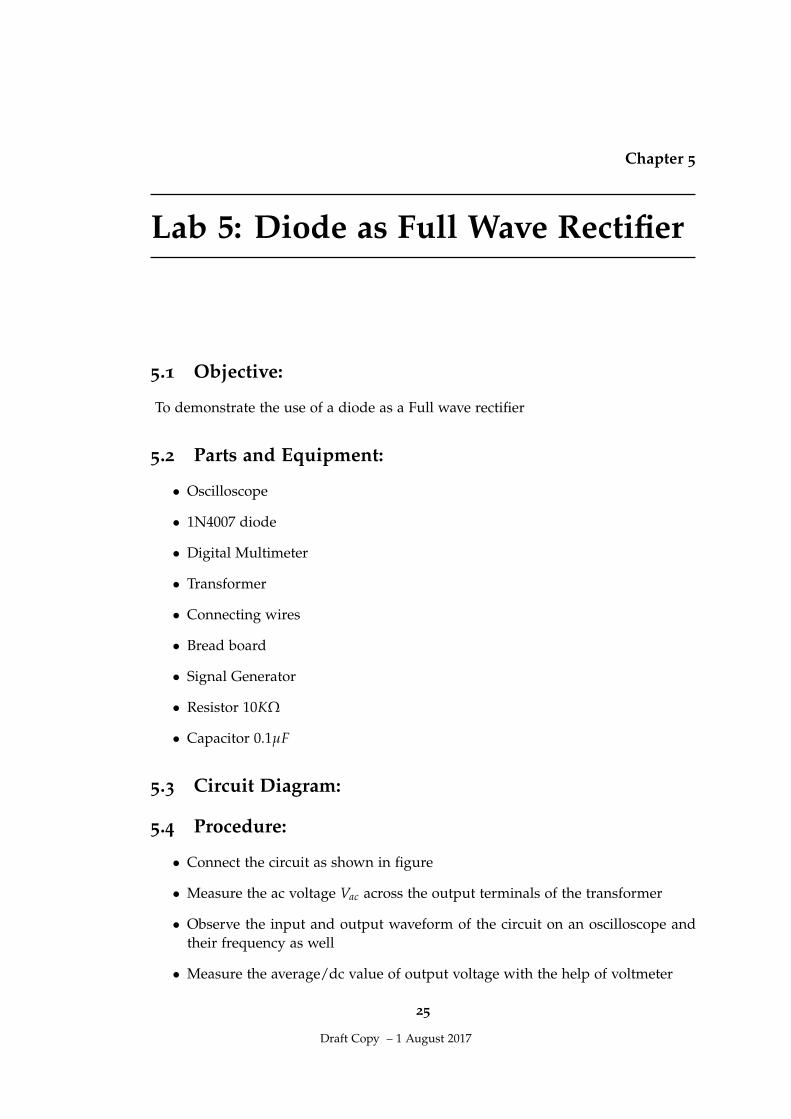
5.3 Circuit Diagram:
5.4 Procedure:
• Connect the circuit as shown in figure
• Measure the ac voltage Vac across the output terminals of the transformer
• Observe the input and output waveform of the circuit on an oscilloscope andtheir frequency as well
• Measure the average/dc value of output voltage with the help of voltmeter
25
Draft Copy – 1 August 2017

26 Lab 5: Diode as Full Wave Rectifier
Figure 5.1: Full Wave Rectifier Circuit
• Calculate average/dc value using the formula and compare
Vdc =2Vmax
π
• Find PIV of the rectifier
Figure 5.2: Input and Output waveform plot
• Measure the average/dc value of output voltage with the help of voltmeter
• Calculate average/dc value using the formula and compare
Vdc =Vmax
π
• Connect oscilloscope across the diode and find the peak value of the sinusoidalwaveform. That will be the PIV of the rectifier
5.5 Efficiency:
• Find Vrms, Irms, Vdc and Idc to calculate the efficiency using the relation:
Vdc =VPR
1+1/2 fr RLC
%r = 12√
3 fr RLC× 100
• Now connect a 100 µF capacitor as shown and observe the output
Draft Copy – 1 August 2017

§5.6 Precautions: 27
Figure 5.3: Rectifier
• Find Vdc and ripple factor using the formula. Also find Vdc using voltmeter andcompare
Vdc =VPR
1+1/2 fr RLC
%r = 12√
3 fr RLC× 100
5.6 Precautions:
• All the connections should be neat and tight
• Multimeter should be checked before performing the experiment
• Resistors and diode should be checked
• Voltage should not be increased to much higher value lest it cause damages tothe circuit
5.7 Course Learning Outcomes
5.8 Review Questions:
1. If the frequency of input voltage is increased, what will be its effects on output?
2. What is the efficiency of the full wave rectifier?
Draft Copy – 1 August 2017

28 Lab 5: Diode as Full Wave Rectifier
Microprocessor Systems Lab RubricPLOs Excellent Good Satisfactory Poor Score
3.0 2.0 1.0 0
ApparatusUsage
PLO-5
Can inde-pendently
setup,operate andhandle theapparatus
Can setupand handle
theapparatus
withminimal
help
Can setupand handle
theapparatuswith some
help
Cannotsetup or
handle theapparatus
DataAcquisition
PLO-5
All requireddata is
recordedand
presentedaccurately
andcompletely
in therequiredformat
Datarecorded
andpresented is
completebut accuracyis not as perrequirement.
Therequiredformat isfollowed.
Datarecorded
andpresented is
partiallycomplete.
Therequiredformat is
followed butwith few
deficiencies.
Datarecordedonly with
considerableassistance
frominstructor
Design PLO-3
Specifications,parameters
andconstraintsof design
arecompletely
present
Specifications,parameters
andconstraintsof design
are partiallypresent
Some speci-fications,
parametersand
constraintsof design
are present
No specifi-cations,
parametersand
constraintsof design
are present
Data Inter-pretation
PLO-4
Analyzesand
interpretsdata
correctly forall tasks/
experimentsin the lab
Analyzesand
interpretsdata
correctly forfew tasks/
experimentsin the lab
Analyzesdata
correctlyhoweverunable to
interpret itfor tasks/
experimentsin the lab
Unable toanalyze and
interpretdata for any
tasks/experiments
in the lab
Total Score in Lab (Out of 12)
Table 5.1: Lab Rubric
Draft Copy – 1 August 2017

§5.8 Review Questions: 29
Figure 5.4: Diode as Half wave Rectifier
3. In a full wave rectifier, how often does the current flow through the load, whenthe inpt cycle is applied? s
Draft Copy – 1 August 2017

30 Lab 5: Diode as Full Wave Rectifier
Draft Copy – 1 August 2017

Chapter 6
Lab 6: Diode as Full Wave BridgeRectifier
6.1 Objective:
To demonstrate the use of a diode as a Full wave bridge rectifier
6.2 Parts and Equipment:
• Oscilloscope
• 1N4007 diode
• Digital Multimeter
• Tranformer
• Connecting wires
• Bread board
• Signal Generator
• Resistor 10KΩ
• Capacitor 0.1µF
6.3 Circuit Diagram:
6.4 Procedure:
• Connect the circuit as shown in figure
• Measure the ac voltage Vac across the output terminals of the transformer
• Observe the input and output waveform of the circuit on an oscilloscope andtheir frequency as well
31
Draft Copy – 1 August 2017
32 Lab 6: Diode as Full Wave Bridge Rectifier
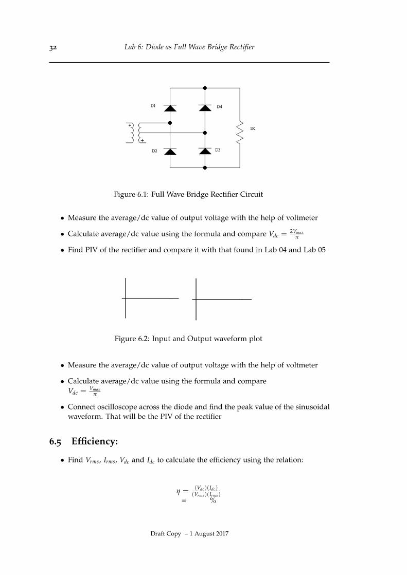
Figure 6.1: Full Wave Bridge Rectifier Circuit
• Measure the average/dc value of output voltage with the help of voltmeter
• Calculate average/dc value using the formula and compare Vdc =2Vmax
π
• Find PIV of the rectifier and compare it with that found in Lab 04 and Lab 05
Figure 6.2: Input and Output waveform plot
• Measure the average/dc value of output voltage with the help of voltmeter
• Calculate average/dc value using the formula and compareVdc =
Vmaxπ
• Connect oscilloscope across the diode and find the peak value of the sinusoidalwaveform. That will be the PIV of the rectifier
6.5 Efficiency:
• Find Vrms, Irms, Vdc and Idc to calculate the efficiency using the relation:
η = (Vdc)(Idc)(Vrms)(Irms)
= %
Draft Copy – 1 August 2017

§6.6 Precautions: 33
Figure 6.3: Bridge Rectifier
• Now connect a 100µF capacitor as shown and observe the output
• Find Vdc and ripple factor using the formula. Also find Vdc using voltmeter andcompare
Vdc =VPR
1+1/2 fr RLC
%r = 12√
3 fr RLC× 100
6.6 Precautions:
• All the connections should be neat and tight
• Multimeter should be checked before performing the experiment
• Resistors and diode should be checked
• Voltage should not be increased to much higher value lest it cause damages tothe circuit
6.7 Course Learning Outcomes
6.8 Review Questions:
1. What is the output frequency of a bridge rectifier?
Draft Copy – 1 August 2017
34 Lab 6: Diode as Full Wave Bridge Rectifier
Microprocessor Systems Lab RubricPLOs Excellent Good Satisfactory Poor Score
3.0 2.0 1.0 0
ApparatusUsage
PLO-5
Can inde-pendently
setup,operate andhandle theapparatus
Can setupand handle
theapparatus
withminimal
help
Can setupand handle
theapparatuswith some
help
Cannotsetup or
handle theapparatus
DataAcquisition
PLO-5
All requireddata is
recordedand
presentedaccurately
andcompletely
in therequiredformat
Datarecorded
andpresented is
completebut accuracyis not as perrequirement.
Therequiredformat isfollowed.
Datarecorded
andpresented is
partiallycomplete.
Therequiredformat is
followed butwith few
deficiencies.
Datarecordedonly with
considerableassistance
frominstructor
Design PLO-3
Specifications,parameters
andconstraintsof design
arecompletely
present
Specifications,parameters
andconstraintsof design
are partiallypresent
Some speci-fications,
parametersand
constraintsof design
are present
No specifi-cations,
parametersand
constraintsof design
are present
Data Inter-pretation
PLO-4
Analyzesand
interpretsdata
correctly forall tasks/
experimentsin the lab
Analyzesand
interpretsdata
correctly forfew tasks/
experimentsin the lab
Analyzesdata
correctlyhoweverunable to
interpret itfor tasks/
experimentsin the lab
Unable toanalyze and
interpretdata for any
tasks/experiments
in the lab
Total Score in Lab (Out of 12)
Table 6.1: Lab Rubric
Draft Copy – 1 August 2017

§6.8 Review Questions: 35
Figure 6.4: Diode as Full wave Rectifier
2. In reference two bridge rectifier, during the first cycle of the AC pulse, howmany diodes are forward biased?
3. What is called frequency of the variations in the DC output voltage of a recti-fier?
Draft Copy – 1 August 2017

36 Lab 6: Diode as Full Wave Bridge Rectifier
4. Which diode has higher rating?
• Bridge rectifier
• Simple rectifier
Draft Copy – 1 August 2017
Chapter 7
Lab 7: Diode in Voltage Multiplier
7.1 Objective:
To demonstrate the operation of voltage multiplier
7.2 Parts and Equipment:
• Oscilloscope
• 1N4007 diode
• Digital Multimeter
• Connecting wires
• Bread board
• Signal Generator
• Transformer
• Resistor 10KΩ
• Capacitor 10 µF, 100µF
7.3 Circuit Diagram:
7.4 Procedure:
• Connect the oscilloscope and measure the peak voltage of the transformer sec-ondary and record
• Measure voltage across C2 by digital Multimeter
• Connect oscilloscope across C2 and record the waveform
37
Draft Copy – 1 August 2017

38 Lab 7: Diode in Voltage Multiplier
Figure 7.1: Diode as Voltage multiplier
Figure 7.2: Input and Output waveform plot
• Find Vdc and ripple factor using the formula. Also find Vdc using voltmeter andcompare
Vdc =VPR
1+1/2 fr RLC
%r = 12√
3 fr RLC× 100
7.5 Precautions:
• All the connections should be neat and tight
• Multimeter should be checked before performing the experiment
• Resistors and diode should be checked
• Voltage should not be increased to much higher value lest it cause damages tothe circuit
7.6 Course Learning Outcomes
7.7 Review Questions:
1. What must be the peak voltage rating of the transformer secondary for a volt-age doubler that produces an output of 200V?
Draft Copy – 1 August 2017

§7.7 Review Questions: 39
Microprocessor Systems Lab RubricPLOs Excellent Good Satisfactory Poor Score
3.0 2.0 1.0 0
ApparatusUsage
PLO-5
Can inde-pendently
setup,operate andhandle theapparatus
Can setupand handle
theapparatus
withminimal
help
Can setupand handle
theapparatuswith some
help
Cannotsetup or
handle theapparatus
DataAcquisition
PLO-5
All requireddata is
recordedand
presentedaccurately
andcompletely
in therequiredformat
Datarecorded
andpresented is
completebut accuracyis not as perrequirement.
Therequiredformat isfollowed.
Datarecorded
andpresented is
partiallycomplete.
Therequiredformat is
followed butwith few
deficiencies.
Datarecordedonly with
considerableassistance
frominstructor
Design PLO-3
Specifications,parameters
andconstraintsof design
arecompletely
present
Specifications,parameters
andconstraintsof design
are partiallypresent
Some speci-fications,
parametersand
constraintsof design
are present
No specifi-cations,
parametersand
constraintsof design
are present
Data Inter-pretation
PLO-4
Analyzesand
interpretsdata
correctly forall tasks/
experimentsin the lab
Analyzesand
interpretsdata
correctly forfew tasks/
experimentsin the lab
Analyzesdata
correctlyhoweverunable to
interpret itfor tasks/
experimentsin the lab
Unable toanalyze and
interpretdata for any
tasks/experiments
in the lab
Total Score in Lab (Out of 12)
Table 7.1: Lab Rubric
Draft Copy – 1 August 2017

40 Lab 7: Diode in Voltage Multiplier
2. What PIV rating of diode be selected for a voltage doubler?
3. How we can increase the current rating of voltage doubler?
4. Which diode has higher rating?
• Bridge rectifier
• Simple rectifier
Draft Copy – 1 August 2017
Chapter 8
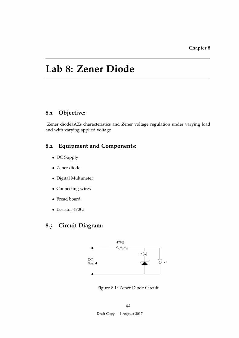
Lab 8: Zener Diode
8.1 Objective:
Zener diodeâAZs characteristics and Zener voltage regulation under varying loadand with varying applied voltage
8.2 Equipment and Components:
• DC Supply
• Zener diode
• Digital Multimeter
• Connecting wires
• Bread board
• Resistor 470Ω
8.3 Circuit Diagram:
Figure 8.1: Zener Diode Circuit
41
Draft Copy – 1 August 2017

42 Lab 8: Zener Diode
8.4 Procedure:
• Connect the circuit as shown in the figure
• Turn on dc supply. Slowly adjust it and measure voltage with the help of digitalmultimeter and record in the following table
• Observe that Zener voltage variation is very small as compared to input voltage
• Draw the graph based upon above values
Table 8.1: Add caption
Sr. No. Iz(mA) Vz(Volts) Vin(Volts
1 5
2 10
3 15
4 20
Figure 8.2: Input and Output waveform plot
• Connect the circuit as shown below
• Set RV to maximum resistance
• Adjust input supply to 20 volts
• Vary RV and adjust IL through RV and record the values in the table below
• Observe that when load current approaches the total current, the voltage acrossthe load begins to decrease and regulation is lost
Draft Copy – 1 August 2017

§8.5 Precautions: 43
Figure 8.3: Zener Diode Circuit
Table 8.2: Add caption
Sr. No. IL(mA) IT(mA) Vin(Volts) Vz(Volts) Iz(mA)
1
2
3
4
5
• Connect the circuit as shown below
• Make input voltage equal to Zener voltage slowly. Decrease the applied voltageto zero and observe that the Zener voltage follows the applied voltage since theZener diode no longer regulates
8.5 Precautions:
• All the connections should be neat and tight
• Multimeter should be checked before performing the experiment
• Resistors and diode should be checked
• Voltage should not be increased to much higher value lest it cause damages tothe circuit
8.6 Course Learning Outcomes
8.7 Review Questions:
1. What is the basic difference between Zener diode and a simple diode?
Draft Copy – 1 August 2017

44 Lab 8: Zener Diode
Microprocessor Systems Lab RubricPLOs Excellent Good Satisfactory Poor Score
3.0 2.0 1.0 0
ApparatusUsage
PLO-5
Can inde-pendently
setup,operate andhandle theapparatus
Can setupand handle
theapparatus
withminimal
help
Can setupand handle
theapparatuswith some
help
Cannotsetup or
handle theapparatus
DataAcquisition
PLO-5
All requireddata is
recordedand
presentedaccurately
andcompletely
in therequiredformat
Datarecorded
andpresented is
completebut accuracyis not as perrequirement.
Therequiredformat isfollowed.
Datarecorded
andpresented is
partiallycomplete.
Therequiredformat is
followed butwith few
deficiencies.
Datarecordedonly with
considerableassistance
frominstructor
Design PLO-3
Specifications,parameters
andconstraintsof design
arecompletely
present
Specifications,parameters
andconstraintsof design
are partiallypresent
Some speci-fications,
parametersand
constraintsof design
are present
No specifi-cations,
parametersand
constraintsof design
are present
Data Inter-pretation
PLO-4
Analyzesand
interpretsdata
correctly forall tasks/
experimentsin the lab
Analyzesand
interpretsdata
correctly forfew tasks/
experimentsin the lab
Analyzesdata
correctlyhoweverunable to
interpret itfor tasks/
experimentsin the lab
Unable toanalyze and
interpretdata for any
tasks/experiments
in the lab
Total Score in Lab (Out of 12)
Table 8.3: Lab Rubric
Draft Copy – 1 August 2017

§8.7 Review Questions: 45
Figure 8.4: Zener Diode
2. What is the function of current limiting resistor in a Zener diode circuit?
3. What happened when the reverse voltage applied to a Zener diode exceeds thebreak-down voltage?
Draft Copy – 1 August 2017

46 Lab 8: Zener Diode
Draft Copy – 1 August 2017
Chapter 9
Lab 9: Common EmitterCharacteristics of BJT
9.1 Objective:
To construct a set of common emitter input and output characteristic curves basedon practical measurement
9.2 Equipment and Components:
• DC Supply
• Transistor C828
• Digital Multimeter
• Connecting wires
• Bread board
• Resistors 100Ω, 1KΩ
• Potentiometers 250K, 10K
• Resistor 470Ω
9.3 Circuit Diagram:
9.4 Procedure:
• To determine the input characteristics of common emitter amplifier, connect thecircuit as shown above
• Adjust 250K and 10K variable resistors to set VCE and VBE as shown in the table.
47
Draft Copy – 1 August 2017

48 Lab 9: Common Emitter Characteristics of BJT
Figure 9.1: BJT Common Emitter Configuration
• Measure and record the voltage across 1K resistor Vb for each combination ofVCE and VBE.
Table 9.1: Add caption
Sr. NoVce = 3 Volts Vce = 5 Volts
Vbe (V) Vb(V) Ib = Vb/Rb (mA) Vbe(V) Vb(V) Ib = Vb/Rb (mA)
• To determine the output characteristics of the common emitter configuration,set the 10K potentiometer to its max value. This will cause VCE to decrease to 0volts.
• Adjust 250K potentiometer to set Ib to some value of ACM/IEEE InternationalSymposium on MicroarchitectureA.
• Adjust the 10K potentiometer for all values of VCE in table making sure that IBremains constant
Draft Copy – 1 August 2017

§9.5 Input Characteristics: 49
Table 9.2: Add caption
Sr. No. VceIb= 10 ÂtA Ib= 20 ÂtA Ib= 30 ÂtA Ib= 40 ÂtA Ib= 50 ÂtA
Vc Ic=Vc/Rc Vc Ic=Vc/Rc Vc Ic=Vc/Rc Vc Ic=Vc/Rc Vc Ic=Vc/Rc
1 0.2
2 0.4
3 0.6
4 0.8
5 1
6 3
7 5
Figure 9.2: Input Characteristics
9.5 Input Characteristics:
9.6 Output Characteristics:
9.7 Precautions:
• All the connections should be neat and tight
• Multimeter should be checked before performing the experiment
• Trasistors, Resistors and diode should be checked
• Voltage should not be increased to much higher value lest it cause damages tothe circuit
Draft Copy – 1 August 2017

50 Lab 9: Common Emitter Characteristics of BJT
Figure 9.3: Output Characteristics
9.8 Course Learning Outcomes
9.9 Review Questions:
1. What elements determine the overall voltage gain of a common emitter ampli-fier?
2. What is the phase relationship of input and output voltages of common emitteramplifier?
3. What is the effect of load on voltage gain of common emitter amplifier?
Draft Copy – 1 August 2017

§9.9 Review Questions: 51
Microprocessor Systems Lab RubricPLOs Excellent Good Satisfactory Poor Score
3.0 2.0 1.0 0
ApparatusUsage
PLO-5
Can inde-pendently
setup,operate andhandle theapparatus
Can setupand handle
theapparatus
withminimal
help
Can setupand handle
theapparatuswith some
help
Cannotsetup or
handle theapparatus
DataAcquisition
PLO-5
All requireddata is
recordedand
presentedaccurately
andcompletely
in therequiredformat
Datarecorded
andpresented is
completebut accuracyis not as perrequirement.
Therequiredformat isfollowed.
Datarecorded
andpresented is
partiallycomplete.
Therequiredformat is
followed butwith few
deficiencies.
Datarecordedonly with
considerableassistance
frominstructor
Design PLO-3
Specifications,parameters
andconstraintsof design
arecompletely
present
Specifications,parameters
andconstraintsof design
are partiallypresent
Some speci-fications,
parametersand
constraintsof design
are present
No specifi-cations,
parametersand
constraintsof design
are present
Data Inter-pretation
PLO-4
Analyzesand
interpretsdata
correctly forall tasks/
experimentsin the lab
Analyzesand
interpretsdata
correctly forfew tasks/
experimentsin the lab
Analyzesdata
correctlyhoweverunable to
interpret itfor tasks/
experimentsin the lab
Unable toanalyze and
interpretdata for any
tasks/experiments
in the lab
Total Score in Lab (Out of 12)
Table 9.3: Lab Rubric
Draft Copy – 1 August 2017

52 Lab 9: Common Emitter Characteristics of BJT
Draft Copy – 1 August 2017

Chapter 10
Lab 10: Common BaseCharacteristics of BJT
10.1 Objective:
To construct a set of common base input and output characteristic curves based onpractical measurement
10.2 Equipment and Components:
• DC Supply
• Transistor C828
• Digital Multimeter
• Connecting wires
• Bread board
• Resistors 4.7KΩ, 22KΩ, 1KΩ
10.3 Circuit Diagram:
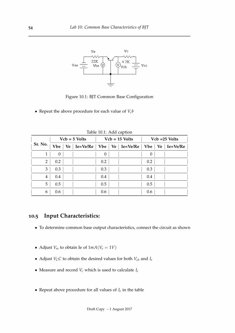
10.4 Procedure:
• To measure transistorâAZs common base characteristics, connect the circuit asshown above
• Adjust Vcc to obtain Vcb of 5V
• Adjust Vee to obtain Vbe of 0V
• Measure and record Ve to determine emitter current Ie
• Repeat the procedure for all values of Vbe in the corresponding column of table
53
Draft Copy – 1 August 2017
54 Lab 10: Common Base Characteristics of BJT
Figure 10.1: BJT Common Base Configuration
• Repeat the above procedure for each value of Vcb
Table 10.1: Add caption
Sr. No.Vcb = 5 Volts Vcb = 15 Volts Vcb =25 Volts
Vbe Ve Ie=Ve/Re Vbe Ve Ie=Ve/Re Vbe Ve Ie=Ve/Re
1 0 0 0
2 0.2 0.2 0.2
3 0.3 0.3 0.3
4 0.4 0.4 0.4
5 0.5 0.5 0.5
6 0.6 0.6 0.6
10.5 Input Characteristics:
• To determine common base output characteristics, connect the circuit as shown
• Adjust Vee to obtain Ie of 1mA(Ve = 1V)
• Adjust VCC to obtain the desired values for both Vcb and Ie
• Measure and record Vc which is used to calculate Ic
• Repeat above procedure for all values of Ie in the table
Draft Copy – 1 August 2017

§10.5 Input Characteristics: 55
Table 10.2: Add caption
Sr No. VcbIe=1mA Ie=2mA Ie=3mA Ie=4mA Ie=5mA
Vc Ic=Vc/Rc Vc Ic=Vc/Rc Vc Ic=Vc/Rc Vc Ic=Vc/Rc Vc Ic=Vc/Rc
1 -0.65
2 -0.5
3 0
4 5
5 10
6 15
7 20
Table 10.3: Add caption
Sr. NoVce = 3 Volts Vce = 5 Volts
Vbe (V) Vb(V) Ib = Vb/Rb (mA) Vbe(V) Vb(V) Ib = Vb/Rb (mA)
Draft Copy – 1 August 2017

56 Lab 10: Common Base Characteristics of BJT
Figure 10.2: Input Characteristics plot
Figure 10.3: Common base output characteristics circuit
10.6 Output Characteristics
• To determine the output characteristics of the common emitter configuration,set the 10K potentiometer to its max value. This will cause VCE to decrease to 0volts.
• Adjust 250K potentiometer to set Ib to some value of ACM/IEEE InternationalSymposium on MicroarchitectureA.
• Adjust the 10K potentiometer for all values of VCE in table making sure that IBremains constant
10.7 Precautions:
• All the connections should be neat and tight
• Multimeter should be checked before performing the experiment
Draft Copy – 1 August 2017

§10.8 Course Learning Outcomes 57
Figure 10.4: Common base output characteristics plot
Table 10.4: Add caption
Sr. No. VceIb= 10 ÂtA Ib= 20 ÂtA Ib= 30 ÂtA Ib= 40 ÂtA Ib= 50 ÂtA
Vc Ic=Vc/Rc Vc Ic=Vc/Rc Vc Ic=Vc/Rc Vc Ic=Vc/Rc Vc Ic=Vc/Rc
1 0.2
2 0.4
3 0.6
4 0.8
5 1
6 3
7 5
• Trasistors, Resistors and diode should be checked
• Voltage should not be increased to much higher value lest it cause damages tothe circuit
10.8 Course Learning Outcomes
10.9 Review Questions:
1. What is a common collector amplifier called?
Draft Copy – 1 August 2017

58 Lab 10: Common Base Characteristics of BJT
Microprocessor Systems Lab RubricPLOs Excellent Good Satisfactory Poor Score
3.0 2.0 1.0 0
ApparatusUsage
PLO-5
Can inde-pendently
setup,operate andhandle theapparatus
Can setupand handle
theapparatus
withminimal
help
Can setupand handle
theapparatuswith some
help
Cannotsetup or
handle theapparatus
DataAcquisition
PLO-5
All requireddata is
recordedand
presentedaccurately
andcompletely
in therequiredformat
Datarecorded
andpresented is
completebut accuracyis not as perrequirement.
Therequiredformat isfollowed.
Datarecorded
andpresented is
partiallycomplete.
Therequiredformat is
followed butwith few
deficiencies.
Datarecordedonly with
considerableassistance
frominstructor
Design PLO-3
Specifications,parameters
andconstraintsof design
arecompletely
present
Specifications,parameters
andconstraintsof design
are partiallypresent
Some speci-fications,
parametersand
constraintsof design
are present
No specifi-cations,
parametersand
constraintsof design
are present
Data Inter-pretation
PLO-4
Analyzesand
interpretsdata
correctly forall tasks/
experimentsin the lab
Analyzesand
interpretsdata
correctly forfew tasks/
experimentsin the lab
Analyzesdata
correctlyhoweverunable to
interpret itfor tasks/
experimentsin the lab
Unable toanalyze and
interpretdata for any
tasks/experiments
in the lab
Total Score in Lab (Out of 12)
Table 10.5: Lab Rubric
Draft Copy – 1 August 2017

§10.9 Review Questions: 59
2. What characteristic common collector amplifier make it a useful circuit?
3. Is there any phase inversion from input to output in a common collector am-plifier?
Draft Copy – 1 August 2017

60 Lab 10: Common Base Characteristics of BJT
Draft Copy – 1 August 2017

Chapter 11
Lab 11: Common CollectorCharacteristics of BJT
11.1 Objective:
To construct a set of common collector input and output characteristic curves basedon practical measurement
11.2 Equipment and Components:
• DC Supply
• Transistor C828
• Digital Multimeter
• Connecting wires
• Bread board
• Resistors 100Ω, 1K|Omega
• Potentiometers 250K, 10K
• Resistors 4.7KΩ, 22KΩ, 1KΩ
11.3 Circuit Diagram:
11.4 Procedure:
• To measure the input characteristics of common collector configuration, connectthe circuit as shown above
• By carefully adjusting potentiometer 250K and 10K, set the voltage Vce and Vcbas shown in the table.
61
Draft Copy – 1 August 2017

62 Lab 11: Common Collector Characteristics of BJT
Figure 11.1: BJT Common Collector Configuration
• Measure and record Vb in the table which will be used to find the value of IB.
• Calculate IB and plot the input characteristics of common collector configura-tion
Table 11.1: Add caption
Sr No.Vce = 3 volts Vce = 5 volts Vce = 7 volts
Vcb Vb Ib=Vb/Rb Vcb Vb Ib=Vb/Rb Vcb Vb Ib=Vb/Rb
1 2.4 4.4 6.4
2 2.38 4.38 6.69
3 2.36 4.36 6.38
4 2.34 4.34 6.36
5 2.32 4.32 6.34
11.5 Input Characteristics:
• To determine the output characteristics of the common collector configuration,set the 10K potentiometer to its max value. This will cause Vce to decrease to 0volts.
• Adjust 250K potentiometer to set Ib to some value of ÎijA.
• Adjust the 10K potentiometer for all values of VCE in table making sure that IBremains constant
Draft Copy – 1 August 2017

§11.6 Output Characteristics 63
Figure 11.2: Input Characteristics plot
11.6 Output Characteristics
11.7 Precautions:
• All the connections should be neat and tight
• Multimeter should be checked before performing the experiment
• Transistors, Resistors and diode should be checked
• Voltage should not be increased to much higher value lest it cause damages tothe circuit
11.8 Course Learning Outcomes
11.9 Review Questions:
1. Why common base configuration is little used practical??
Draft Copy – 1 August 2017

64 Lab 11: Common Collector Characteristics of BJT
Table 11.2: Add caption
Sr No. VceIb=10ÎijA Ib=20ÎijA Ib=30ÎijA Ib=40ÎijA Ib=50ÎijA
Ve Ie=Ve/Re Ve Ie=Ve/Re Ve Ie=Ve/Re Ve Ie=Ve/Re Ve Ie=Ve/Re
1 0.2
2 0.4
3 0.6
4 0.8
5 1
6 3
7 5
2. 2Can the same voltage gain be achieved with a common base as with a commonemitter amplifier?
3. 3. What is the main disadvantage of common base amplifier as compared tocommon emitter and emitter follower amplifier?
Draft Copy – 1 August 2017

§11.9 Review Questions: 65
Microprocessor Systems Lab RubricPLOs Excellent Good Satisfactory Poor Score
3.0 2.0 1.0 0
ApparatusUsage
PLO-5
Can inde-pendently
setup,operate andhandle theapparatus
Can setupand handle
theapparatus
withminimal
help
Can setupand handle
theapparatuswith some
help
Cannotsetup or
handle theapparatus
DataAcquisition
PLO-5
All requireddata is
recordedand
presentedaccurately
andcompletely
in therequiredformat
Datarecorded
andpresented is
completebut accuracyis not as perrequirement.
Therequiredformat isfollowed.
Datarecorded
andpresented is
partiallycomplete.
Therequiredformat is
followed butwith few
deficiencies.
Datarecordedonly with
considerableassistance
frominstructor
Design PLO-3
Specifications,parameters
andconstraintsof design
arecompletely
present
Specifications,parameters
andconstraintsof design
are partiallypresent
Some speci-fications,
parametersand
constraintsof design
are present
No specifi-cations,
parametersand
constraintsof design
are present
Data Inter-pretation
PLO-4
Analyzesand
interpretsdata
correctly forall tasks/
experimentsin the lab
Analyzesand
interpretsdata
correctly forfew tasks/
experimentsin the lab
Analyzesdata
correctlyhoweverunable to
interpret itfor tasks/
experimentsin the lab
Unable toanalyze and
interpretdata for any
tasks/experiments
in the lab
Total Score in Lab (Out of 12)
Table 11.3: Lab Rubric
Draft Copy – 1 August 2017

66 Lab 11: Common Collector Characteristics of BJT
Figure 11.3: Common Collector output plot
Draft Copy – 1 August 2017

Chapter 12
Lab 12: Metal Oxide SemiconductorField Effect Transistor
12.1 Objective:
To investigate the drain characteristics of a MOSFET
12.2 Equipment and Components:
• Two DC Supplies
• MOSFET
• Digital Multimeter
• Connecting wires
• Bread board
• Resistors 100KΩ, 1KΩ, 4.7K
• item Potentiometers 100K, 1K
12.3 Circuit Diagram:
12.4 Procedure:
• Connect the circuit as shown above
• Turn potentiometers fully counter clock wise, and turn on power supply
• Leave 100K potentiometer fully counter clock wise so that VGS = 0
• Adjust 1K potentiometer to get desired values of Vds as shown in the table
67
Draft Copy – 1 August 2017

68 Lab 12: Metal Oxide Semiconductor Field Effect Transistor
Figure 12.1: MOSFET
Table 12.1: Add caption
Vgs= 0 volts
Vds (volts) 1 2 3 4 5 6 7 8
Id (mA)
• Measure voltage across 1K resistor. Use this value to find out the value of Idand fill in the corresponding place in the above table
• Adjust 100K potentiometer so that VGS = −0.5 volts
• Repeat above steps to find VDS and Id and fill the table below
Table 12.2: Add caption
Vgs= -0.5 volts
Vds (volts) 1 2 3 4 5 6 7 8
Id (mA)
• Invert the leads of the supply connected to the gate of the MOSFET and adjustthe 100K potentiometer so that VGS = 0.5 volts
• Repeat above steps to find VDS and Id and fill the table below
• Use the corresponding values of Id and Vds to draw the drain characteristics
Draft Copy – 1 August 2017
§12.5 Transfer Characteristics: 69
Table 12.3: Add caption
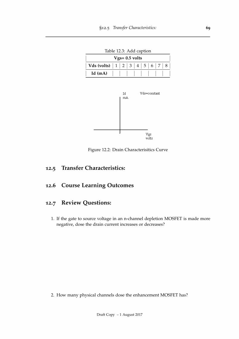
Vgs= 0.5 volts
Vds (volts) 1 2 3 4 5 6 7 8
Id (mA)
Figure 12.2: Drain Characterisitics Curve
12.5 Transfer Characteristics:
12.6 Course Learning Outcomes
12.7 Review Questions:
1. If the gate to source voltage in an n-channel depletion MOSFET is made morenegative, dose the drain current increases or decreases?
2. How many physical channels dose the enhancement MOSFET has?
Draft Copy – 1 August 2017

70 Lab 12: Metal Oxide Semiconductor Field Effect Transistor
Microprocessor Systems Lab RubricPLOs Excellent Good Satisfactory Poor Score
3.0 2.0 1.0 0
ApparatusUsage
PLO-5
Can inde-pendently
setup,operate andhandle theapparatus
Can setupand handle
theapparatus
withminimal
help
Can setupand handle
theapparatuswith some
help
Cannotsetup or
handle theapparatus
DataAcquisition
PLO-5
All requireddata is
recordedand
presentedaccurately
andcompletely
in therequiredformat
Datarecorded
andpresented is
completebut accuracyis not as perrequirement.
Therequiredformat isfollowed.
Datarecorded
andpresented is
partiallycomplete.
Therequiredformat is
followed butwith few
deficiencies.
Datarecordedonly with
considerableassistance
frominstructor
Design PLO-3
Specifications,parameters
andconstraintsof design
arecompletely
present
Specifications,parameters
andconstraintsof design
are partiallypresent
Some speci-fications,
parametersand
constraintsof design
are present
No specifi-cations,
parametersand
constraintsof design
are present
Data Inter-pretation
PLO-4
Analyzesand
interpretsdata
correctly forall tasks/
experimentsin the lab
Analyzesand
interpretsdata
correctly forfew tasks/
experimentsin the lab
Analyzesdata
correctlyhoweverunable to
interpret itfor tasks/
experimentsin the lab
Unable toanalyze and
interpretdata for any
tasks/experiments
in the lab
Total Score in Lab (Out of 12)
Table 12.4: Lab Rubric
Draft Copy – 1 August 2017

§12.7 Review Questions: 71
Figure 12.3: Transfer Characteristics
3. What is the difference between MOSFET JFET?
Draft Copy – 1 August 2017

72 Lab 12: Metal Oxide Semiconductor Field Effect Transistor
Draft Copy – 1 August 2017

Chapter 13
Lab 12: Junction Field EffectTransistor
13.1 Objective:
To investigate the drain characteristics of a JFET
13.2 Equipment and Components:
• Two DC Supplies
• JFET
• Digital Multimeter
• Connecting wires
• Bread board
• Resistors 100KΩ, 100ω, 1KΩ
• Potentiometers 100K, 1K
13.3 Circuit Diagram:
13.4 Procedure:
• Connect the circuit as shown above
• Turn potentiometers fully counter clock wise, and turn on power supply
• Leave 100K potentiometer fully counter clock wise so that VGS = 0
• Adjust 1K potentiometer to get desired values of VDS as shown in the table
73
Draft Copy – 1 August 2017

74 Lab 12: Junction Field Effect Transistor
Figure 13.1: MOSFET
Table 13.1: Add caption
Vgs= 0 volts
Vds (volts) 1 2 3 4 5 6 7 8
Id (mA)
• Measure voltage across 1K resistor. Use this value to find out the value of IDand fill in the corresponding place in the above table
• Now adjust 100K potentiometer so that VGS = −0.25 volts.
• Repeat above steps to find Vds and Id and fill the table below:
Table 13.2: Add caption
Vgs= -0.25 volts
Vds (volts) 1 2 3 4 5 6 7 8
Id (mA)
• Now adjust 100K potentiometer so that VGS = −0.5 volts.
• Repeat above steps to find VDS and ID and fill the table below
• Now adjust 100K potentiometer so that VGS = −0.75 volts.
• Repeat above steps to find VDS and ID and fill the table below
• Use the corresponding values of ID and VDS to draw the drain characteristics
Draft Copy – 1 August 2017

§13.5 Transfer Characteristics: 75
Table 13.3: Add caption
Vgs= -0.50 volts
Vds (volts) 1 2 3 4 5 6 7 8
Id (mA)
Table 13.4: Add caption
Vgs= -0.75 volts
Vds (volts) 1 2 3 4 5 6 7 8
Id (mA)
13.5 Transfer Characteristics:
13.6 Course Learning Outcomes
13.7 Review Questions:
1. In which bias mode, dose the JFET operates?
2. Is JFET unipolar or bipolar device?
3. Should a P-channel JFET have a positive or negative Vgs?
Draft Copy – 1 August 2017

76 Lab 12: Junction Field Effect Transistor
Microprocessor Systems Lab RubricPLOs Excellent Good Satisfactory Poor Score
3.0 2.0 1.0 0
ApparatusUsage
PLO-5
Can inde-pendently
setup,operate andhandle theapparatus
Can setupand handle
theapparatus
withminimal
help
Can setupand handle
theapparatuswith some
help
Cannotsetup or
handle theapparatus
DataAcquisition
PLO-5
All requireddata is
recordedand
presentedaccurately
andcompletely
in therequiredformat
Datarecorded
andpresented is
completebut accuracyis not as perrequirement.
Therequiredformat isfollowed.
Datarecorded
andpresented is
partiallycomplete.
Therequiredformat is
followed butwith few
deficiencies.
Datarecordedonly with
considerableassistance
frominstructor
Design PLO-3
Specifications,parameters
andconstraintsof design
arecompletely
present
Specifications,parameters
andconstraintsof design
are partiallypresent
Some speci-fications,
parametersand
constraintsof design
are present
No specifi-cations,
parametersand
constraintsof design
are present
Data Inter-pretation
PLO-4
Analyzesand
interpretsdata
correctly forall tasks/
experimentsin the lab
Analyzesand
interpretsdata
correctly forfew tasks/
experimentsin the lab
Analyzesdata
correctlyhoweverunable to
interpret itfor tasks/
experimentsin the lab
Unable toanalyze and
interpretdata for any
tasks/experiments
in the lab
Total Score in Lab (Out of 12)
Table 13.5: Lab Rubric
Draft Copy – 1 August 2017

§13.7 Review Questions: 77
Figure 13.2: Drain Characteristics Curve
Figure 13.3: Transfer Characteristics
Draft Copy – 1 August 2017

78 Lab 12: Junction Field Effect Transistor
Draft Copy – 1 August 2017