
Plasticity of indium nanostructures as revealed by synchrotron X-ray microdiffraction
Upload
independentCategory
view
0download
0
i n t e r n a t i o n a l j o u r n a l o f h y d r o g e n en e r g y 3 6 ( 2 0 1 1 ) 6 5 1 9e6 5 2 8
Avai lab le a t www.sc iencedi rec t .com
journa l homepage : www.e lsev ier . com/ loca te /he
Efficient H2 production by water-splitting usingindiumetin-oxide/V-doped TiO2 multilayer thinfilm photocatalyst
R. Dholam*, N. Patel, A. Miotello
Dipartimento di Fisica, Universita degli Studi di Trento, I-38123 Povo (Trento), Italy
a r t i c l e i n f o
Article history:
Received 29 November 2010
Received in revised form
28 February 2011
Accepted 7 March 2011
Available online 6 April 2011
Keywords:
Photocatalytic water-splitting
Hydrogen generation
V-doped TiO2
RF-magnetron sputtering
Visible light irradiation
Multilayer
Charge recombination
* Corresponding author. Tel.: þ39 3478267397E-mail address: [email protected] (R
0360-3199/$ e see front matter Copyright ªdoi:10.1016/j.ijhydene.2011.03.028
a b s t r a c t
In order to sensitize TiO2 in visible light and to reduce photo-induced charge recombination,
the multilayer films of IndiumeTin Oxide (ITO)/V-doped TiO2 were synthesized by radio-
frequency magnetron sputtering. V-doped TiO2 thin films showed red shift in TiO2 absorp-
tion edge with increasing dopant concentration and, most importantly, the dopant energy
levels are formed in the TiO2 band gap due to V5þ/V4þ ions as confirmed by UVeVisible and
XPS spectra. Multilayer films with different numbers of ITO/V-doped TiO2 (6 at.%) bilayers
(namely, 2-, 3-, 4-, 5-, 6- and 7-bilayers) were deposited, in order to reduce the charge
recombination rate, by keeping the total thickness of TiO2 constant in each multilayer film.
In multilayer films, when exposed to visible light the photocurrent increases as function of
the number of bilayers by reaching the maximum with 6-bilayers of ITO/V-doped TiO2. The
measured enhanced photocurrent is attributed to: 1) ability of V-doped TiO2 to absorb visible
light, 2) number of space-charge layers in form of ITO/TiO2 interfaces inmultilayer films, and
3) generation of photoelectrons just in/or near to the space-charge layer by decreasing the V-
doped TiO2 layer thickness. The reduced charge recombination rate in multilayer films was
also confirmed by the photocurrent kinetic curves. The superior photocatalytic efficiency of
the 6-bilayers film is also reflected in hydrogen production rate through water-splitting: we
obtained indeed 31.2 mmol/h of H2 production rate.
Copyright ª 2011, Hydrogen Energy Publications, LLC. Published by Elsevier Ltd. All rights
reserved.
1. Introduction splitting such as: i) high resistant to corrosion and photo-
It is extremely important to use clean and renewable energy
sources such as solar and wind for hydrogen production
which is presently produced (about 95%) from fossil fuels by
procedures that lead to increase in greenhouse gases [1].
Photocatalytic water-splitting by using solar energy could
contribute to the solution of environmental and energy issues
related to the hydrogen production [2].
TiO2 semiconductor provides several advantages over other
materialsasaphotocatalyst forhydrogenproductionbywater-
.. Dholam).2011, Hydrogen Energy P
corrosion in aqueous media, ii) cheap and easily available, iii)
environmentally clean, iv) energy band edges which are well-
matched with the redox level of water, and v) electronic
properties that can be varied by just changing the lattice
defects chemistry or the oxygen stoichiometry [3]. In addition,
TiO2 is also the most desired material for self-cleaning tech-
nology and in purification of toxic compounds from polluted
water and air [4e6]. However, because of thewide energy band
gap (w3.2 eV) of TiO2, only a small fraction of solar spectrum,
UV light (3e5% of total), can be used for photocatalytic
ublications, LLC. Published by Elsevier Ltd. All rights reserved.

i n t e rn a t i o n a l j o u r n a l o f h y d r o g e n en e r g y 3 6 ( 2 0 1 1 ) 6 5 1 9e6 5 2 86520
processes [7]. Thus, the efficient utilization of the solar spec-
trum (mainly a good portion of visible light) is one of the
important subjects for developing the future generation of
TiO2-based photocatalysts. Doping TiO2 with foreign ions is
one of the most promising strategies for sensitizing TiO2 to
visible light by forming impurity levels in the forbidden gap [8].
DopingTiO2with 3d-transitionmetals (V, Cr,Mn, Fe, Co, and
Ni) is the best approach to decrease the band gap or to establish
energy levels inside the band gap leading to significant visible
light absorption for TiO2 [9e13]. However, these doping ions
alsocontribute in reducing the lifetimeofphoto-inducedcharge
carriers in doped TiO2. Thus an increased recombination rate of
charge carriers in doped TiO2 implies a reduction of the photo-
catalytic activity. Choi et al. [10] investigated the photocatalytic
activity of TiO2 doped with 21 different metal ions and proved
that both dopant type and concentration are the important
aspects to control the recombination processes. Doping with
small concentration of transition metals (lower than 1 at.%) in
TiO2 successfully reduced the recombination processes by
introducing traps for electrons and/or holes [11]. However, the
low concentration doping does not cause significant increase in
theabsorptionof the visible light inTiO2. Anefficientnarrowing
of theTiO2bandgap isachievedwithhighdopantconcentration
(about 5e10 at.%), but at the same time it introduces new
recombination centers for the photo-generated charges thus
increasing recombination processes [14]. From previous
consideration, it becomes important to solve the problem of
recombination for these moderately doped TiO2.
By using redox couple as electrolyte inside the photo-elec-
trochemical cell can reduce the recombination processes to
some extent on the surface of semiconductor [15,16]. In addi-
tion, application of an external bias can also offer better charge
separation. But both these solutions are not convenient for
commercial purposes related to solar energy conversion. More
convenient route to suppress the recombination processes is to
produce specific charge states to favor electrons and holes
trapping while having appropriate spatial separation. This can
be accomplished by coupling two semiconductor layers such
that the edge of the conduction band of the first semiconductor
is lower than that of the second one. If the semiconductor
layers are not much thick, then the photo-generated electrons
in one layer are easily injected into the second one [17]. In
addition, a thin space-charge layer of a few tens of nanometers
is formed near the interface of the semiconductors to make
their Fermi level equal [18]. The junction electric field is built up
in this space-charge layer of the electrode and is able to provide
the driving force to displace the photo-generated electrons
from one semiconductor to another thus favoring the electron-
hole separation. Thus creating number of interfaces or space-
charge layers in the photo-electrode provides better solution
for the problem related to recombination of charges. Many
TiO2-based coupled systems such as CdS/TiO2 [19], WO3/TiO2
[20], SnO2/TiO2 [21], SiO2/TiO2 [22] etc., have been used in the
past as photocatalysts. However, none was reported using
transition-metal -doped TiO2 in the coupled system where the
recombination rates are paramount.
In our previous work [23], we succeeded in reducing the
recombination rates of photo-generated charges by adopting
the ITO/Cr-doped TiO2 multilayer film structure with a number
of bilayers. Now in the present work we further check the
efficiency of the multilayer structure in increasing both charge
separation and charge-transfer, by using a different dopant
metal, namely V. TiO2 filmswere dopedwithV-metal, using co-
sputtering deposition technique, to enhance the visible light
absorption efficiency while depositing ITO/TiO2 multilayers for
reduction of the charge recombination rates. The photo-
catalytic efficiency of the multilayer-based TiO2 photo-elec-
trode was tested by measuring hydrogen production through
water-splitting in photo-electrochemical cell.
2. Experimental
RF-magnetron sputteringwasused to synthesize undoped- and
V-doped TiO2 thin films. Pure TiO2 disc (purity equal to 99.99%)
and Ar gas (purity equal to 99.99%) were used as sputtering
target and working gas, respectively. Before deposition, high
vacuumwith base pressure of<3� 10�5 Pawas attained, while
during deposition Ar pressure of 0.8 Pa was maintained in the
chamber. V-doped TiO2 films were synthesized by partially
covering the TiO2 target surfacewith small V-metal pellets. The
number of pellets on the TiO2 target was varied in order to
obtainV-doped filmsof four different atomic concentrations. In
order to remove any surface contamination the TiO2 target was
pre-sputtered for 20 min before film deposition. The TiO2 films
were sputter-deposited on both glass and Si (100) substrates at
room temperature using RF power of 150W. The sample-target
distance was kept constant at 5.5 cm for deposition of all the
samples. After deposition, no post annealing was performed.
TiO2 thin films were deposited on a conducting indiumetin
oxide (ITO) layer which provides electrical back contact to test
photocatalytic activity. The ITO layer, of about 80 nm, was
deposited on the glass slide before the deposition of TiO2 film
using magnetron sputtering with RF power of 100 W and
working Ar gas pressure of 0.8 Pa. Pre-sputtering of the ITO
target was also conducted to remove possible surface contam-
ination. Multilayer film was prepared by sequential in-situ
sputtering of ITO layer and then of V-doped TiO2: this forms
a single bilayer. Similarly, several numbers of bilayers (2-, 3-, 4-,
5-, 6- and 7-bilayers) were deposited in order to study the effi-
ciency of the multilayer structure in reducing recombination
ratesofholes andelectrons. The total thickness ofV-dopedTiO2
was kept constant, about 750 nm, in all the multilayer films by
controlling the sputtering deposition time. Thus, as the bilayer
number increases, the thickness of the V-doped TiO2 decreases
in each bilayer to maintain the constant total thickness of all
TiO2 films. The thickness of ITO (w80 nm) was kept constant in
all the multilayer films irrespective of number of bilayers. The
surfaces of all the films, that will be in contact with the elec-
trolyte, were always covered with pure TiO2 of w100 nm to
protect the metal ions from leaching out in the electrolyte.
The structural characterization of themultilayeredV-doped
TiO2 films was carried out by X-ray diffraction (XRD) technique
(Cu Ka radiation, l ¼ 1.5414 A�) in Bragg-Brentano (qe2q)
configuration. Surface electronic states of the photocatalyst
were established by using X-ray photoelectron spectroscopy
(XPS). X-ray photoelectrons spectra were acquired using an
SCIENTAESCA200 instrumentequippedwithamonochromatic
AlKa (1486.6 eV)X-Ray source and ahemispherical analyzer.No
electrical charge compensation was required to perform XPS
10 20 30 40 50 60 70
Inten
sit
y (A
rb
. u
nit
s)
2θ (Degree)
Pure TiO2
V 2 at%
V 4 at%
V 5 at%
V 6 at%
Anatase
Rutile
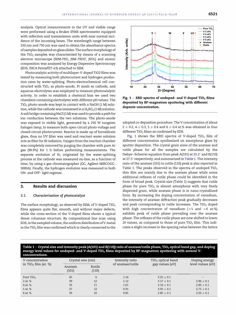
Fig. 1 e XRD spectra of undoped- and V-doped TiO2 films
deposited by RF-magnetron sputtering with different
dopants concentration.
i n t e r n a t i o n a l j o u r n a l o f h y d r o g e n en e r g y 3 6 ( 2 0 1 1 ) 6 5 1 9e6 5 2 8 6521
analysis. Optical measurements in the UV and visible range
were performed using a Bruker IFS66 spectrometer equipped
with reflection and transmission units with near normal inci-
dence of the incoming beam. The wavelength range between
250 nm and 750 nmwas used to obtain the absorbance spectra
of samplesdepositedonglassslides.Thesurfacemorphologyof
the TiO2 samples was characterized by means of a scanning
electron microscope (SEM-FEG, JSM-7001F, JEOL) and atomic
composition was analyzed by Energy Dispersive Spectroscopy
(EDS, INCA PentaFET-x3) attached to SEM.
Photocatalytic activity ofmultilayer-V-dopedTiO2filmswas
tested by measuring both photocurrent and hydrogen produc-
tion rates by water-splitting. Photo-electrochemical cell con-
structed with TiO2 as photo-anode, Pt mesh as cathode, and
aqueous electrolytes was employed to measure photocatalytic
activity. In order to establish a chemical bias we used two
chambers containing electrolytes with different pH values. The
TiO2 photo-anode was kept in contact with a NaOH (1 M) solu-
tion, while the cathodewas immersed in aH2SO4 (1M) solution.
AsaltbridgecontainingNaCl (1M)wasusedtoprovideapath for
ion conduction between the two solutions. The photo-anode
was exposed to visible light, generated by a 250 W tungsten
halogen lamp, to measure both open-circuit photo-voltage and
closed-circuit photocurrent. Reactor is made up of borosilicate
glass, thus no UV filter was used and reactant water solution
acts as filter for IR radiation. Oxygen from the reaction chamber
was completely removed by purging the chamber with pure Ar
gas (99.9%) for 1 h before performing measurements. The
separate evolution of H2 originated by the water-splitting
process at the cathode was measured on-line, as a function of
time, by using a gas chromatographer (GC, Agilent MIRCOGC-
3000A). Finally, the hydrogen evolution was measured in both
ON- and OFF- light regimes.
3. Results and discussion
3.1. Characterization of photocatalyst
The surface morphology, as observed by SEM, of V-doped TiO2
films appears quite flat, smooth, and without major defects,
while the cross-section of the V-doped films shows a typical
dense columnar structure. By compositional line scan using
EDS, inthesampledvolume, theuniformdistributionofV-metal
in theTiO2 filmwas confirmedwhich is clearly connected to the
Table 1e Crystal size and intensity peak (A(101) and R(110)) ratienergy level values for undoped- and V-doped TiO2 films depoconcentrations.
V concentrationin TiO2 film (at. %)
Crystal size (nm) Intenof ana
Anatase(101)
Rutile(110)
Pure TiO2 45 6
2 at. % 39 12
4 at. % 35 11
5 at. % 37 12
6 at. % 39 10
adopted co-deposition procedure. The V concentration of about
2 � 0.2, 4 � 0.3, 5 � 0.4 and 6 � 0.4 at.% was obtained in four
different TiO2 films as confirmed by EDS.
Fig. 1 shows the XRD spectra of V-doped TiO2 film of
different concentration synthesized on amorphous glass by
sputter deposition. The crystal grain sizes of the anatase and
rutile phase for all the samples are calculated by the
DebyeeScherrer equation from peak A(101) at 25.2� and R(110)
at 27.5� respectively, and summarized in Table 1. The intensity
ratio of the anatase (101) to rutile (110) peak is also reported in
Table 1. The peaks observed in the spectra of undoped TiO2
thin film are mainly due to the anatase phase while some
additional reflexes of rutile phase could be identified in the
form of broad peak. Crystal size (Table 1) suggests that rutile
phase for pure TiO2 is almost amorphous with very finely
dispersed grain, while anatase phase is in nano-crystallized
form. By increasing the doping concentration of vanadium,
the intensity of anatase diffraction peak gradually decreases
and peak corresponding to rutile increases. The TiO2 doped
with high concentration of vanadium (w5 and w6 at.%)
exhibits peak of rutile phase prevailing over the anatase
phase. The reflexes of the rutile phase are now shifted to lower
2q values, as compared to those of pure TiO2 film. This indi-
cates a slight increase in the spacing value between the lattice
o of anatase/rutile phase, TiO2 optical band gap, and dopingsited by RF-magnetron sputtering with several V-
sity ratiotase/rutile
TiO2 optical bandgap values (eV)
Doping energylevel values (eV)
1.14 3.25 � 0.1 e
1.12 3.17 � 0.1 2.96 � 0.1
1.01 3.10 � 0.1 2.83 � 0.1
0.91 3.05 � 0.1 2.75 � 0.1
0.81 2.85 � 0.1 2.50 � 0.1

i n t e rn a t i o n a l j o u r n a l o f h y d r o g e n en e r g y 3 6 ( 2 0 1 1 ) 6 5 1 9e6 5 2 86522
planes which might be caused by the insertion of V in the
lattice. No characteristic peaks due to vanadium oxides (V2O5
or VO2) were detected in XRD pattern. These results indicate
that V ions are incorporated into the TiO2 lattice and promote
the anatase-to-rutile phase transformation. Zhao et al. [24]
have reported that upon increasing the vanadium concen-
tration, the anatase-to-rutile transformation was promoted
due to a lattice distortion of anatase caused by vanadium
incorporation, which favors transformation to rutile.
XPS was carried out to confirm the concentrations and to
determine the chemical states of V in the samples. Fig. 2a and
b show the XPS spectra of Ti2p and V2p electronic levels,
respectively, for pure TiO2 and V-doped TiO2 (w6 at.%). For pure
TiO2, two peaks, namely Ti2p3/2 and Ti2p1/2, appear at 459.35 and
465.09 eV that correspond to þ4 valence state of Ti in the
samples. For V-doped TiO2, the Ti2p peaks position was slightly
shifted by 0.35 eV towards positive binding energy value thus
proving that V ions are incorporated into TiO2 lattice and influ-
encing the local chemical state of Ti4þ ions. To achieve local
charge balance in the TiO2 lattice, some of the Ti ions may
acquire higher oxidation state by releasing electrons, a process
that explains theXPSpeak shift for V-dopedTiO2. XPS spectrum
of V2p3/2 level was deconvoluted into two peaks having binding
energy values of 517.3 and 516.2 eV attributed to V5þ and V4þ
states of vanadium respectively. This indicates that V species
exist in the lattice of TiO2 in the formofV5þ andV4þwith higher
525 520 515 510
V4+2p3/2
Binding Energy (eV)
In
te
ns
ity
(A
br. U
nits
)
V5+2p3/2
V5+2p1/2
V2p
470 465 460 455 450
Ti4+2p
3/2
Ti4+2p
1/2
Ti2p
Pure TiO2
V-doped TiO2
In
ten
sity (A
br.U
nits)
Binding Energy (eV)
a
b
Fig. 2 e X-ray photoelectrons spectra of (a) Ti2p and (b) V2p
levels for pure TiO2 and V-doped TiO2 (6 at.%).
content of V5þ ions as indicated by the area under the peak in
XPS spectrum (Fig. 2b).
The optical properties of the pure and V-doped TiO2 were
studied by measuring the absorption spectra ranging from UV
(250 nm) to visible (750 nm) wavelengths and presented in
Fig. 3. Using Tauc plot (Fig. 4), i.e. (ahy)1/2 versus (hy) (where, a is
the absorbance, h is Planck’s constant, and y is frequency), the
band gap energies were deduced by extrapolating the linear
region of the plot to intersect the photon energy axis: the
obtained values are reported in Table 1. The figures clearly
show a slight shift in the absorption band edge towards longer
wavelengths when increasing the V concentration in the TiO2
film. Most importantly the tail of the absorption band is
observed, indicating the existence of additional energy levels in
the band gap. This can be related to the charge-transfer from
the d orbital of V5þ and V4þ to the conduction band of TiO2. For
VeTiO2, V5þ and V4þ ions are incorporated into the TiO2 lattice
which forms three kinds of isolated impurity energy levels just
below the bottom of the TiO2 conduction band (CB) [25].
Because of these impurity energy levels in the band gap, the
electrons in the valence band can be excited to the impurity
energy levels and then subsequently excited to the CB by
absorption of visible light. This means that these impurity
energy levels are beneficial for extending the absorption spec-
trum wavelength towards the visible light region.
3.2. Photocurrent measurement
The above results indicates that 6 at.% V-doped TiO2 shows the
maximum lowering of the photon-absorbed energy due to the
impurity energy levels in visible range. Thus photocatalytic
activity measurements were carried out only with 6 at.%
V-dopedTiO2film (henceforth thisfilmwill bedesignatedasV6-
dopedTiO2 film) bymaking comparisonwith undopedTiO2. V6-
doped TiO2 film (about 750 nm thick) was deposited on an ITO
layer (80 nm), previously deposited on glass substrate. In order
to protect the film from possible corrosion induced by contact
with the electrolyte the obtained bilayer was covered with thin
layer of pure TiO2 (100 nm) and later this single-bilayer filmwas
used as the photo-electrode for water-splitting experiments.
350 400 450 500
Ab
so
rb
an
ce (A
rb
.u
nit)
Wavelength(nm)
V-2 at% V-4 at% V-5 at% V-6 at% TiO 2
Fig. 3 e UVeVIS absorption spectra of undoped- and
V-doped TiO2 films deposited by RF-magnetron sputtering
with different dopants concentration.

Fig. 4 e Tauc plot of undoped- and V-doped TiO2 films
deposited by RF-magnetron sputtering with different
dopants concentration.
Fig. 5 e SEM Images, in back scattering mode, of multilayer
film with 6-bilayers of ITO/V6-doped TiO2.
i n t e r n a t i o n a l j o u r n a l o f h y d r o g e n en e r g y 3 6 ( 2 0 1 1 ) 6 5 1 9e6 5 2 8 6523
The undoped TiO2 film with total thickness of 850 nm was
similarly deposited on an ITO layer (80 nm) for the comparison.
The ITO layer provides the necessary electrical path for the
photo-generated electron from TiO2 to Pt electrode. Most
importantly the ITO/TiO2 stack film is able to partially limit the
recombination of photo-generated holes and electrons (hþ and
e�) because the conduction band edge of ITO (w�4.5 eV) is at an
energy value lower than that of TiO2 (w�4.0 eV) thus making
favorable for the injection of electrons from the later into the
former.
The photo-induced voltage and current are measured for
undoped- and V6-doped TiO2 in light-ON regime in photo-
electrochemical cell with open- and closed-circuit configura-
tion, respectively. The open-circuit photo-voltage value
results more than w1.4 V, for both these TiO2 samples, which
is greater than the required voltage (1.23 V) to break the water
molecule. However, the photocurrent measured using V6-
doped TiO2 (w53 mA) is negligible as compared to pure TiO2
films (w290 mA) in the light-ON regime. This is mainly due to
recombination of the photo-generated charges on defects
associated to the dopant V5þ/V4þ ions.
To efficiently suppress the charge recombination rates it is
important to immediately remove the photoelectron from the
generation site before it recombines with the holes through
radiative or non-radiative processes. This fast separation can
be achieved by coupling two semiconductors with appropriate
conduction energy levels. For instance, as mentioned previ-
ously, in the ITO/TiO2 coupled system, the conduction band
edge of ITO (w�4.5 eV) is at an energy value lower than that of
TiO2 (w�4.0 eV) thus making favorable for the injection of
electrons from the later into the former. Once the photoelec-
tron from TiO2 is injected in ITO, it has a very low probability
of back transfer and, as a result, electrons and holes are
definitely separated. However, to be efficient, ITO should be
located near the electron generation site to provide the driving
force for the photoelectron transfer.
Following the above strategy, we have depositedmultilayer
films with different numbers (2-, 3-, 4-, 5-, 6- and 7-bilayers) of
ITO/V6-doped TiO2 bilayers and finally covering with thin
layer of pure TiO2 (100 nm) the surface layer that will be in
contact with the electrolyte. The bottom portion of the overall
multilayers (see Fig. 7b below) is also in contact with the
electrolyte through the pure TiO2 (100 nm) layer (while the
corresponding top portion is electrically connected to cathode
of the photo-electrochemical cell). In all the multilayer films
the total thickness of V6-doped TiO2 was kept constant
(750 nm) by decreasing the thickness of each V6-doped TiO2
layer when increasing the number of the bilayers. The thick-
ness of ITO (w80 nm) was kept constant in all the multilayer
films irrespective of number of bilayers.
The cross-section SEM image, in back scattering mode, of
a multilayer film with 6-bilayers of ITO/V6-doped TiO2 is
presented in Fig. 5. The white layer of ITO can be easily
distinguished from the dark layer of V6-doped TiO2 and for
this reason both the periodicity and continuity of the layers
are clearly visible. The Fig. 6 shows the thickness of single
V6-TiO2 layer, measured through cross-section SEM images,
as a function of number of bilayers. The figure confirms that as
the number of bilayers increases, the thickness of single
V6-doped TiO2 layer decreases.
ITO is a transparent conducting oxide with a direct band
gap in the range of 3.9e4.2 eV which is significantly higher
than the absorption edge of V6-doped TiO2 layer thus ITO
deposited on the top of TiO2 layer does not affect the amount
of photons reaching the TiO2 layer. This feature was experi-
mentally confirmed by measuring the absorbance of the V6-
doped TiO2eITO bilayers, with ITO on top, in the UVeVisible
range: the spectra showed similar red shift in the band edge as
that observed with single layer.
Photo-catalytic activity of themultilayer filmswas tested by
using ITO/V6-doped TiO2 multilayer films as photo-anode in
photo-electrochemical cell and measuring photo-voltage and
photocurrent for light-ON regime. Each ITO layer in the multi-
layer films is electrically connected to theplatinumcathodeand
so as soon as the electrons are injected from the V6-doped TiO2
layers into the ITO layers, they are immediately transferred to
the cathode. The measured photo-voltage of all the multilayer
films (more than 1.4 V)was always greater than that required to
split the water molecule. Fig. 6 reports the measured photo-
current as a function of number of bilayers. During the
measurements, the same surface area (13.75 cm2) is exposed to
the light for allmultilayer films.As thenumberof ITO/V6-doped
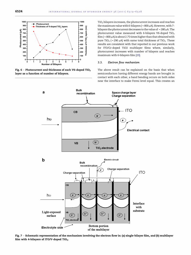
Fig. 6 e Photocurrent and thickness of each V6-doped TiO2
layer as a function of number of bilayers.
Fig. 7 e Schematic representation of the mechanism involving th
film with 4-bilayers of ITO/V-doped TiO2.
i n t e rn a t i o n a l j o u r n a l o f h y d r o g e n en e r g y 3 6 ( 2 0 1 1 ) 6 5 1 9e6 5 2 86524
TiO2 bilayers increases, the photocurrent increases and reaches
themaximumvaluewith6-bilayers (w800mA).However,with7-
bilayers thephotocurrentdecreases tothevalueofw280mA.The
photocurrent value measured with 6-bilayers V6-doped TiO2
film(w800mA) isabout2.75 timeshigher thanthatobtainedwith
pure TiO2 (w290 mA) with same total thickness of TiO2. These
results are consistent with that reported in our previous work
for ITO/Cr-doped TiO2 multilayer films where, similarly,
photocurrent increases with number of bilayers and reaches
maximumwith 6-bilayers film [23].
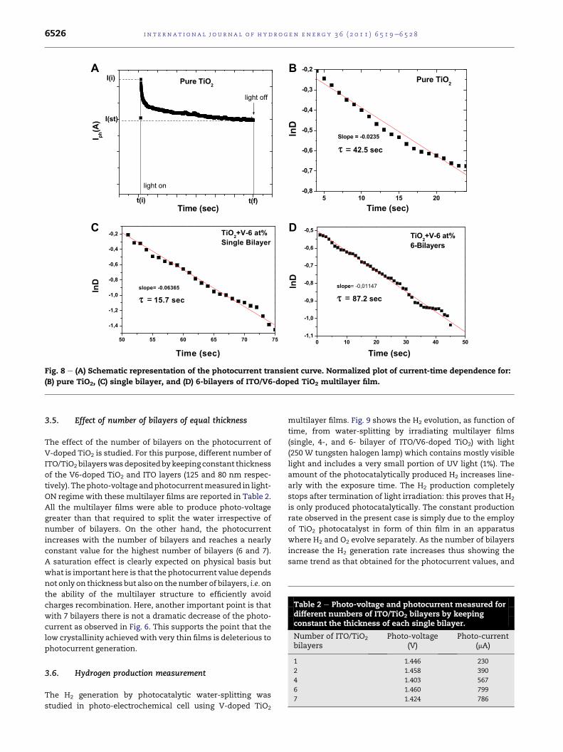
3.3. Electron flow mechanism
The above result can be explained on the basis that when
semiconductors having different energy bands are brought in
contact with each other, a band bending occurs on both sides
near the interface to make Fermi level equal. This creates an
e electron flow in: (a) single-bilayer film, and (b) multilayer

i n t e r n a t i o n a l j o u r n a l o f h y d r o g e n en e r g y 3 6 ( 2 0 1 1 ) 6 5 1 9e6 5 2 8 6525
interface space-charge layer having thickness of several tens of
nanometers where a large electric field is developed. When
photo-electrons are generated in this interface region (or very
near) they are instantaneously pushed out to the adjacent
semiconductor due to the driving force provided by the electric
field and the electron-hole separation is definitely obtained,
a process well known in pen junction semiconductors. Simi-
larly in the present ITO/TiO2 system, the interface region pres-
entselectrical features thatprovideanefficient route for the eeh
separation. Hence by adopting a multilayer structure, we are
abletoproducemanyinterfacesof ITO/TiO2whichestablishfast
transport channels along with efficient eeh separation.
A scheme is reported in Fig. 7 to understand in detail the
mechanismof the electronflow in themultilayer filmsandhow
the number of bilayers affects the generation of the photocur-
rent. The photocurrentmeasuredwith single bilayer of ITO/V6-
doped TiO2 film (Fig. 7a) is very low due to the presence of only
one interface of ITO/V6-doped TiO2 with the thick layer of
V6-doped TiO2 (750 nm) over it (Fig. 7a). Most of the photo-
electronsaregenerated in thebulkof thedopedTiO2where they
have to travel some distance within the TiO2 itself before
entering the space-charge region of the interface to feel the
driving electric field for final injection into ITO. In addition, the
probability of eeh recombination is much higher in V6-doped
TiO2due to thepresenceofrecombinationsitesassociated to the
V5þ/V4þ ions. On contrary, the photocurrent increases signifi-
cantly from w53 mA (for single-bilayer film) to w456 mA by
depositing 4-bilayers film. In this film, the previous V6-doped
TiO2 layer having thickness of 750 nm was divided into four
layers of w185 nm by introducing three more ITO layers. The
resulting film now contains seven ITO/TiO2 interfaces where
space-charge layer is formedand thedecreased thicknessof the
V6-doped TiO2 layers assures that the photo-generated elec-
trons have to travel a short distance into TiO2 (the unshielded
region) before being injected into the ITO layer where recombi-
nation is definitely hindered (Fig. 7b). Another relevant point to
be considered is that in single-bilayer film the photo-electrons,
generated in the V6-doped TiO2 layer, have to move only along
one direction towards the ITO layer placed at the one end of the
layered structure. On the contrary, in multilayer film each
V6-doped TiO2 layer is sandwiched between the two ITO layers
and so the photo-electrons canmove along either of two direc-
tions toavoid recombination (Fig.7b).All thesereasons favor the
increment of the photocurrent in the 4-bilayers film.
Linear increment in the photocurrent as increase in the bila-
yersnumberwasobserved.This ismainlyattributed to thebetter
conditions for charge separation and transport with reduced
number of recombination processes: here we have to further
underline the key role of number of ITO/TiO2 interfaces. The
measured photocurrent reaches the maximum value (w800 mA)
with 6-bilayers film; the measured photocurrent is one order of
magnitude higher than that measured with single-bilayer film
(w53mA). For6-bilayersfilm, thethicknessofV6-dopedTiO2 layer
(125 nm) in each bilayermay be lower than the total thickness of
the space-charge layer of the pertinent interface. Thus photo-
electrons generated in the V6-doped TiO2 are already in space-
charge region where the electric field provides them the driving
force to be instantaneously injected into the ITO layers: this
means that the 6-bilayers film creates the best conditions for
charge separation. In addition, this film is able to absorb more
visible light than pure TiO2 due to the V5þ/V4þ impurity energy
levels, hence generating higher amount of photoelectrons. With
7-bilayersfilmthephotocurrentdecreases (Fig.6);wesuggest this
might be due to the poor crystalline degree of very thin films of
TiO2 (92 nm). Takahashi et al. [26] andNasr et al. [17] showed the
increase in photocurrent by decreasing the TiO2 layer thickness
attaining maximum photocurrent value at particular thickness.
Below this thickness the photocurrent decreases drastically and,
as indicated by the authors, this is attributed to the low crystal-
linity achievedwith thinner films. For themomentwith our XRD
setup it is difficult to acquire the spectra of such a thin layer of
TiO2.However,wewilladdress thisopenproblemwithdedicated
experiments in the future.
3.4. Photocurrent kinetic studies
The better charge separation and reduced recombination
processes observed with multilayer films was further analyzed
by studying the photocurrent kinetics curve. Fig. 8A shows the
schematicdiagramofphotocurrent transient curve. Initially the
anodic photocurrent spike (I(i)) is obtained after the exposure of
light which ismainly due to the separation of the electron-hole
pairs bymovement ofholes towards the semiconductor surface
where they are trapped or reduced by the species in the elec-
trolyte, while the electrons are transported to the back contact.
After I(i) has been attained, the photocurrent decays with time,
owing to the charge recombination processes, until a steady-
state photocurrent (I(st)) is reached. The holes reaching the
semiconductorsurfacemay, insteadofcapturingelectronsfrom
the electrolyte, accumulate at the surface and recombine with
electronsfromtheconductionband, i.e. thedecay isdetermined
by the rate at which minority carriers trapped at surface states
capturemajoritycarriers [27].Thephotocurrenttransientcanbe
defined by the following kinetic equation [28]:
D ¼ exp
��ts
�(1)
Where D is defined as
D ¼ IðtÞ � IðstÞIðiÞ � IðstÞ (2)
Here, s is the transient timeconstant, I(t) is the current at time
t, I(i) is the current at t ¼ 0, and I(st) is the stationary current.
Fig. 8B, C, andD show the plot of lnD vs. time for pure TiO2 film,
single bilayer, and 6-bilayers of ITO/V6-doped TiO2 films,
respectively. The slope of this plot provides swhich is related to
the time for charge recombination processes in the films. The
measured s for V6-doped TiO2 with single-bilayer film is about
three times lower than that for the undoped TiO2. Specifically,
thephotocurrentdecayswithinafewseconds inV-dopedTiO2 is
due to recombinationof thephoto-generatedchargesondefects
associated to the V5þ/V4þ ions. On the contrary, with 6-bilayers
the transient time constant is about two times greater than that
forundopedTiO2filmwhere there arenodefect sites. Thisagain
proves that by introducing space-charge regions in form of ITO/
TiO2 interfaces and by decreasing the thickness of TiO2 layer
favors charge separation while recombination processes are
suppressed even if recombination sites such as V5þ/V4þ are still
present.
5 10 15 20
-0,8
-0,7
-0,6
-0,5
-0,4
-0,3
-0,2
ln
D
Time (sec)
Pure TiO2
Slope = -0.0235
= 42.5 sec
B
50 55 60 65 70 75
-1,4
-1,2
-1,0
-0,8
-0,6
-0,4
-0,2
C
ln
D
Time (sec)
TiO2+V-6 at%
Single Bilayer
slope= -0.06365
= 15.7 sec
light off
t(f)
I ph(A
)
Time (sec)
I(i)
I(st)
t(i)
light on
Pure TiO2
A
0 10 20 30 40 50
-1,1
-1,0
-0,9
-0,8
-0,7
-0,6
-0,5DTiO
2+V-6 at%
6-Bilayers
ln
D
Time (sec)
slope= -0,01147
= 87.2 sec
Fig. 8 e (A) Schematic representation of the photocurrent transient curve. Normalized plot of current-time dependence for:
(B) pure TiO2, (C) single bilayer, and (D) 6-bilayers of ITO/V6-doped TiO2 multilayer film.
Table 2 e Photo-voltage and photocurrent measured fordifferent numbers of ITO/TiO2 bilayers by keepingconstant the thickness of each single bilayer.
Number of ITO/TiO2
bilayersPhoto-voltage
(V)Photo-current
(mA)
i n t e rn a t i o n a l j o u r n a l o f h y d r o g e n en e r g y 3 6 ( 2 0 1 1 ) 6 5 1 9e6 5 2 86526
3.5. Effect of number of bilayers of equal thickness
The effect of the number of bilayers on the photocurrent of
V-doped TiO2 is studied. For this purpose, different number of
ITO/TiO2 bilayerswasdepositedbykeeping constant thickness
of the V6-doped TiO2 and ITO layers (125 and 80 nm respec-
tively). Thephoto-voltage andphotocurrentmeasured in light-
ON regime with these multilayer films are reported in Table 2.
All the multilayer films were able to produce photo-voltage
greater than that required to split the water irrespective of
number of bilayers. On the other hand, the photocurrent
increases with the number of bilayers and reaches a nearly
constant value for the highest number of bilayers (6 and 7).
A saturation effect is clearly expected on physical basis but
what is important here is that the photocurrent value depends
not only on thickness but also on the number of bilayers, i.e. on
the ability of the multilayer structure to efficiently avoid
charges recombination. Here, another important point is that
with 7 bilayers there is not a dramatic decrease of the photo-
current as observed in Fig. 6. This supports the point that the
low crystallinity achievedwith very thin films is deleterious to
photocurrent generation.
1 1.446 230
2 1.458 390
4 1.403 567
6 1.460 799
7 1.424 786
3.6. Hydrogen production measurement
The H2 generation by photocatalytic water-splitting was
studied in photo-electrochemical cell using V-doped TiO2
multilayer films. Fig. 9 shows the H2 evolution, as function of
time, from water-splitting by irradiating multilayer films
(single, 4-, and 6- bilayer of ITO/V6-doped TiO2) with light
(250 W tungsten halogen lamp) which contains mostly visible
light and includes a very small portion of UV light (1%). The
amount of the photocatalytically produced H2 increases line-
arly with the exposure time. The H2 production completely
stops after termination of light irradiation: this proves that H2
is only produced photocatalytically. The constant production
rate observed in the present case is simply due to the employ
of TiO2 photocatalyst in form of thin film in an apparatus
where H2 and O2 evolve separately. As the number of bilayers
increase the H2 generation rate increases thus showing the
same trend as that obtained for the photocurrent values, and
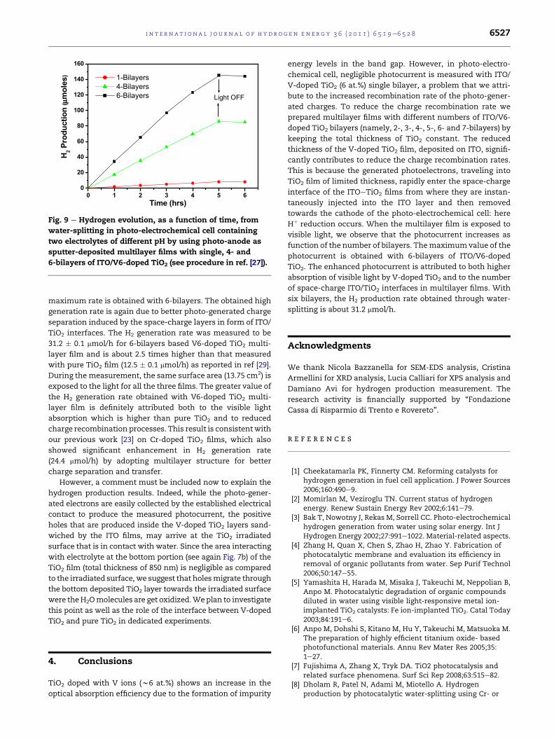
Fig. 9 e Hydrogen evolution, as a function of time, from
water-splitting in photo-electrochemical cell containing
two electrolytes of different pH by using photo-anode as
sputter-deposited multilayer films with single, 4- and
6-bilayers of ITO/V6-doped TiO2 (see procedure in ref. [27]).
i n t e r n a t i o n a l j o u r n a l o f h y d r o g e n en e r g y 3 6 ( 2 0 1 1 ) 6 5 1 9e6 5 2 8 6527
maximum rate is obtained with 6-bilayers. The obtained high
generation rate is again due to better photo-generated charge
separation induced by the space-charge layers in form of ITO/
TiO2 interfaces. The H2 generation rate was measured to be
31.2 � 0.1 mmol/h for 6-bilayers based V6-doped TiO2 multi-
layer film and is about 2.5 times higher than that measured
with pure TiO2 film (12.5 � 0.1 mmol/h) as reported in ref [29].
During the measurement, the same surface area (13.75 cm2) is
exposed to the light for all the three films. The greater value of
the H2 generation rate obtained with V6-doped TiO2 multi-
layer film is definitely attributed both to the visible light
absorption which is higher than pure TiO2 and to reduced
charge recombination processes. This result is consistentwith
our previous work [23] on Cr-doped TiO2 films, which also
showed significant enhancement in H2 generation rate
(24.4 mmol/h) by adopting multilayer structure for better
charge separation and transfer.
However, a comment must be included now to explain the
hydrogen production results. Indeed, while the photo-gener-
ated electrons are easily collected by the established electrical
contact to produce the measured photocurrent, the positive
holes that are produced inside the V-doped TiO2 layers sand-
wiched by the ITO films, may arrive at the TiO2 irradiated
surface that is in contact with water. Since the area interacting
with electrolyte at the bottom portion (see again Fig. 7b) of the
TiO2 film (total thickness of 850 nm) is negligible as compared
to the irradiated surface, we suggest that holesmigrate through
the bottom deposited TiO2 layer towards the irradiated surface
were theH2Omolecules are get oxidized.Weplan to investigate
this point as well as the role of the interface between V-doped
TiO2 and pure TiO2 in dedicated experiments.
4. Conclusions
TiO2 doped with V ions (w6 at.%) shows an increase in the
optical absorption efficiency due to the formation of impurity
energy levels in the band gap. However, in photo-electro-
chemical cell, negligible photocurrent is measured with ITO/
V-doped TiO2 (6 at.%) single bilayer, a problem that we attri-
bute to the increased recombination rate of the photo-gener-
ated charges. To reduce the charge recombination rate we
prepared multilayer films with different numbers of ITO/V6-
doped TiO2 bilayers (namely, 2-, 3-, 4-, 5-, 6- and 7-bilayers) by
keeping the total thickness of TiO2 constant. The reduced
thickness of the V-doped TiO2 film, deposited on ITO, signifi-
cantly contributes to reduce the charge recombination rates.
This is because the generated photoelectrons, traveling into
TiO2 film of limited thickness, rapidly enter the space-charge
interface of the ITOeTiO2 films from where they are instan-
taneously injected into the ITO layer and then removed
towards the cathode of the photo-electrochemical cell: here
Hþ reduction occurs. When the multilayer film is exposed to
visible light, we observe that the photocurrent increases as
function of the number of bilayers. Themaximumvalue of the
photocurrent is obtained with 6-bilayers of ITO/V6-doped
TiO2. The enhanced photocurrent is attributed to both higher
absorption of visible light by V-doped TiO2 and to the number
of space-charge ITO/TiO2 interfaces in multilayer films. With
six bilayers, the H2 production rate obtained through water-
splitting is about 31.2 mmol/h.
Acknowledgments
We thank Nicola Bazzanella for SEM-EDS analysis, Cristina
Armellini for XRD analysis, Lucia Calliari for XPS analysis and
Damiano Avi for hydrogen production measurement. The
research activity is financially supported by “Fondazione
Cassa di Risparmio di Trento e Rovereto”.
r e f e r e n c e s
[1] Cheekatamarla PK, Finnerty CM. Reforming catalysts forhydrogen generation in fuel cell application. J Power Sources2006;160:490e9.
[2] Momirlan M, Veziroglu TN. Current status of hydrogenenergy. Renew Sustain Energy Rev 2002;6:141e79.
[3] Bak T, Nowotny J, Rekas M, Sorrell CC. Photo-electrochemicalhydrogen generation from water using solar energy. Int JHydrogen Energy 2002;27:991e1022. Material-related aspects.
[4] Zhang H, Quan X, Chen S, Zhao H, Zhao Y. Fabrication ofphotocatalytic membrane and evaluation its efficiency inremoval of organic pollutants from water. Sep Purif Technol2006;50:147e55.
[5] Yamashita H, Harada M, Misaka J, Takeuchi M, Neppolian B,Anpo M. Photocatalytic degradation of organic compoundsdiluted in water using visible light-responsive metal ion-implanted TiO2 catalysts: Fe ion-implanted TiO2. Catal Today2003;84:191e6.
[6] Anpo M, Dohshi S, Kitano M, Hu Y, Takeuchi M, Matsuoka M.The preparation of highly efficient titanium oxide- basedphotofunctional materials. Annu Rev Mater Res 2005;35:1e27.
[7] Fujishima A, Zhang X, Tryk DA. TiO2 photocatalysis andrelated surface phenomena. Surf Sci Rep 2008;63:515e82.
[8] Dholam R, Patel N, Adami M, Miotello A. Hydrogenproduction by photocatalytic water-splitting using Cr- or

i n t e rn a t i o n a l j o u r n a l o f h y d r o g e n en e r g y 3 6 ( 2 0 1 1 ) 6 5 1 9e6 5 2 86528
Fe-doped TiO2 composite thin films photocatalyst. Int JHydrogen Energy 2009;34:5337e46.
[9] Ni M, Leung MKH, Leung DYC, Sumathy K. A review andrecent developments in photocatalytic water-splitting usingTiO2 for hydrogen production. Renew Sustain Energy Rev2007;11:401e25.
[10] Choi WY, Termin A, Hoffmann MR. The role of metal iondopants in quantum-sized TiO2: correlation betweenphotoreactivity and charge carrier recombination dynamics.J Phys Chem 1994;84:13669e79.
[11] Litter MI, Navıo JA. Photocatalytic properties of iron-dopedtitania semiconductors. J Photochem Photobio A Chem 1996;98:171e81.
[12] Khan MA, Woo SI, Yang OB. Hydrothermally stabilized Fe(III)doped titania active under visible light for water splittingreaction. Int J Hydrogen Energy 2008;33:5345.
[13] Zhu J, Deng Z, Chen F, Zhang J, Chen H, Anpo M, et al.Hydrothermal doping method for preparation of Cr3þ-TiO2
photocatalysts with concentration gradient distribution ofCr3þ. Appl Catal B Environ 2006;62:329e35.
[14] Radecka M, Rekas M, Trenczek-Zajac A, Zarrzewska K.Importance of the band gap energy and flat band potentialfor application of modified TiO2 photoanodes in waterphotolysis. J Power Sources 2008;181:46e55.
[15] Kozlova EA, Korobkina TP, Vorontsov AV, Parmon VN.Enhancement of the O2 or H2 photoproduction rate in a Ce3þ/Ce4þeTiO2 system by the TiO2 surface and structuremodification. Appl Catal A Gen 2009;367:130e7.
[16] Abe R, Sayama K, Arakawa H. Significant influence of solventon hydrogen production from aqueous I3
�/I� redox solutionusing dye-sensitized Pt/TiO2 photocatalyst under visible lightirradiation. Chem Phys Lett 2003;379:230e5.
[17] Nasr C, Kamat PV, Hotchandani S. Photoelectrochemistry ofcomposite semiconductor thin films. Photosensitization ofthe SnO2/TiO2 coupled system with a ruthenium polypyridylcomplex. J Phys Chem B 1998;102:10047e56.
[18] Morrison SR. Electrochemistry at semiconductor andoxidized metal electrodes. New York: Plenum Press; 1984.
[19] Chi Y, Fu H, Qi L, Shi K, Zhang H, Yu H. Preparation andphotoelectric performance of ITO/TiO2/CdS composite thinfilms. J Photochem Photobio A Chem 2008;195:357e63.
[20] Akurati KK, Vital A, Dellemann JP, Michalow K, Graule T,Ferri D, et al. Flame-made WO3/TiO2 nanoparticles: Relationbetween surface acidity, structure and photocatalyticactivity. Appl Catal B Environ 2008;79:53e62.
[21] Shang J, Yao W, Zhu Y, Wu N. Structure and photocatalyticperformances of glass/SnO2/TiO2 interface composite film.Appl Catal A Gen 2004;257:25e32.
[22] Beyers E, Biermans E, Ribbens S, De Witte K, Mertens M,Meynen V, et al. Combined TiO2/SiO2 mesoporousphotocatalysts with location and phase controllable TiO2
nanoparticles. Appl Catal B Environ 2009;88:515e24.[23] Dholam R, Patel N, Santini A, Miotello A. Efficient indium tin
oxide/Cr-doped-TiO2 multilayer thin films for H2 productionby photocatalytic water-splitting. Int J Hydrogen Energy 2010;35:9581e90.
[24] ZhaoG,KozukaH,LinH,YokoT.Sol-gelpreparationofTi1-xVxO2
solid solution film electrodes with conspicuous photoresponsein the visible region. Thin Solid Films 1999;339:123e8.
[25] Zhou W, Liu Q, Zhu Z, Ji Z. Preparation and properties ofvanadium-doped TiO2 photocatalysts. J Phys D Appl Phys2010;43:035301e6.
[26] Takahashi M, Tsukigi K, Uchino T, Yoko T. Enhancedphotocurrent in thin film TiO2 electrodes prepared by solegelmethod. Thin Solid Films 2001;388:231e6.
[27] Hagfeldt A, Lindstrom H, Sodergren S, Lindquist SE.Photoelectrochemical studies of colloidal TiO2 films: theeffect of oxygen studied by photocurrent transient. JElectroanal Chem 1995;381:39e46.
[28] Redecka M, Wierzbicka M, Komornicki S, Rekas M. Influenceof Cr on photoelectrochemical properties of TiO2 thin films.Physica B 2004;348:160e8.
[29] Dholam R, Patel N, Adami M, Miotello A. Physically andchemically synthesized TiO2 composite thin films forhydrogen production by photocatalytic water splitting. Int JHydrogen Energy 2008;33:6896e903.
Copyright © 2022 FDOKUMEN


![Low-Cost TiO[sub 2] Photocatalytic Technology for Water Potabilization in Plastic Bottles For Isolated Regions. Photocatalyst Fixation](https://static.fdokumen.com/doc/165x107/633786bbd102fae1b60768d8/low-cost-tiosub-2-photocatalytic-technology-for-water-potabilization-in-plastic.jpg)