Electrolytic Etching Copper and Silver Using Copper Nitrate, a ...
Upload
independentCategory
view
0download
0
University of Nebraska - LincolnDigitalCommons@University of Nebraska - LincolnFaculty Publications from the Department ofElectrical Engineering Electrical Engineering, Department of
1-1-2008
EX-SITU AND IN-SITU SELENIZATION OFCOPPER-INDIUM AND COPPER-BORONTHIN FILMSRodney J. SoukupUniversity of Nebraska - Lincoln, [email protected]
Natale J. IannoUniversity of Nebraska - Lincoln, [email protected]
Chad KamlerUniversity of Nebraska - Lincoln
Martin DiazUniversity of Nebraska - Lincoln
Shuchi SharmaUniversity of Nebraska - Lincoln
See next page for additional authors
This Article is brought to you for free and open access by the Electrical Engineering, Department of at DigitalCommons@University of Nebraska -Lincoln. It has been accepted for inclusion in Faculty Publications from the Department of Electrical Engineering by an authorized administrator ofDigitalCommons@University of Nebraska - Lincoln. For more information, please contact [email protected].
Soukup, Rodney J.; Ianno, Natale J.; Kamler, Chad; Diaz, Martin; Sharma, Shuchi; Huguenin-Love, James; and Olejnicek, Jiri, "EX-SITU AND IN-SITU SELENIZATION OF COPPER-INDIUM AND COPPER-BORON THIN FILMS" (2008). FacultyPublications from the Department of Electrical Engineering. Paper 121.http://digitalcommons.unl.edu/electricalengineeringfacpub/121

AuthorsRodney J. Soukup, Natale J. Ianno, Chad Kamler, Martin Diaz, Shuchi Sharma, James Huguenin-Love, and JiriOlejnicek
This article is available at DigitalCommons@University of Nebraska - Lincoln: http://digitalcommons.unl.edu/electricalengineeringfacpub/121

EX-SITU AND IN-SITU SELENIZATION OF COPPER-INDIUM AND COPPER-BORON THIN FILMS
R. J. Soukup1, N. J. lann0 1, Chad Kamler 1, Martin Diaz 1, Shuchi Sharma 1, James Huguenin-Love 1,Jifi Olejnicek 2,
Scott A. Darveau 2, Christopher L. Exstrom 2,
1. Department of Electrical Engineering University of Nebraska-Lincoln, Lincoln, NE 68588-0511
2. Department of Chemistry University of Nebraska at Kearney, Kearney, NE 66849-1150
ABSTRACT
It has recently been established that the ideal bandgap for terrestrial photovoltaics is 1.37 eV and the bandgap for CulnSe2 is only around 1.04 eV. Thus, a larger bandgap is needed. However, neither the substitution of Ga nor of AI has made a high efficiency solar cell absorber with a band gap of 1.37 eV possible. B, an even smaller atom, should require less atomic substitution than either Ga or AI to achieve a wider bandgap. In order to fabricate a thin film of CulnxB1-xSe2 (CIBS), Cu, In and B were deposited from a variety of sputtering targets which were pure Cu, In, and B; a CU.45ln.ss; and a CU3B2 target. Films were deposited simultaneously and sequentially. After deposition these films were post selenized in another vacuum chamber. Analysis of these films was accomplished using Raman spectroscopy, X-ray diffraction (XRD), and Auger electron spectroscopy (AES). With the difficulties encountered, materials were also deposited in a selenium atmosphere.
INTRODUCTION
A recent paper by Contreras, et. al. has set the optimum absorber bandgap for terrestrial solar cells at 1.37 eV [1] and the bandgap for CulnS~ (CIS) is reported to be about 1.04 eV, [2] although bandgaps have been reported from 0.8 eV [3] to 1.18 eV [4] depending on the method of fabrication. To increase the bandgaps, various element substitutions, such as Ga and AI for In and S for Se, have been investigated. To date, the substitution of Ga for In has been the most successful resulting in an efficiency of 19.9% [5). Although no CulnxB1-xSe2 (CIBS) films have been reported, a simple approach was used to estimate that the amount of B substitution needed to reach a bandgap of 1.37 eV. This calculation showed that less than 19% B is needed [6). The copper, indium and boron materials in the films were deposited simultaneously and sequentially in respective methods. After deposition these films were post selenized in another vacuum chamber. The results of the analyses of these films indicate that the films grown sequentially in a quasi layered manner were the most successful. The initial results presented illustrate the difficulties encountered in making a CIBS material using the post selenization technique. With the difficulties encountered the materials were also deposited in a
978-1-4244-1641-7/08/$25.00 ©2008 IEEE
selenium atmosphere. The deposition of the Cu, In, and B in the Se vapor was made necessary by the migration of the CIS material to the front of the film during the selenization process, leaving the boron to accumulate at the substrate surface [7]. This migration was discovered by a set of experiments using Auger analysis which will be illustrated in this presentation.
POST DEPOSITION SELENIZA TION
The deposition of precursor thin films which were then selenized was accomplished using three different techniques. These techniques were simultaneous deposition of Cu, In and/or B, deposition of Cu and In preceded by or followed by the deposition of B, and the quasi-layered technique in which the substrates were rotated to receive depositions of Cu and In in a sequential manner. We refer to this as a quasi-layered technique because the next material deposited, i.e. In after Cu is incident upon the substrate before a complete monolayer of Cu is deposited.
The best results were achieved with the quasilayering of Cu and In. The results of measurements made on these films are presented below.
Simultaneous Deposition
The series of thin films fabricated by simultaneous deposition of Cu and In or of Cu, In and B were post selenized by the technique of heating in a Se vapor [8,9). The results of these experiments will be published elsewhere [7]. Of importance here is that the precursor films deposited exhibited Auger electron spectroscopy (AES) depth profiling results just as expected, i.e. the materials were of approximately the proper concentrations and the magnitudes of the signals were constant throughout the entire film. When selenized the X-ray diffraction (XRD) and Raman spectroscopy results indicated CIS films were being formed. These results were as expected for the selenization of the Culn layers, unfortunately the results were the same for the CulnxB1-x as for the Culn films. In order to understand what was happening, AES depth profiling measurements were made. In each case, regardless of the amount of B incorporated into the film, CulnSe y was found at the top of
33rd IEEE Photovoltaic Specialists Conference, 2008. PVSC '08. Digital Object Identifier: 10.1109/PVSC.2008.4922546
Publication Year: 2008 , Page(s): 1 - 6
the films and B had migrated to the back and presented a barrier to further selenization. Because of the difficulty in determining the elemental sensitivity for AES in such a previously unreported film, the value of y is unknown.
Boron on Copper Indium or Copper Indium on Boron
In order to determine whether this behavior was typical and to determine if we could selenize B or CuB films of these materials were deposited first and then covered with a film of Culn. In every case, B was left at the bottom of the film and prevented a barrier to further selenization. The top portion of the films again appeared to be CIS.
When B was deposited onto Culn and selenization took place, the film on top was again CIS on a film of B, i.e. the boron migrated to the back of the film. This led to the experiment which indicated what is happening. The sequence of figures, figures 6a through 6d in the above reference [9] illustrate the process quite well. The sequence is a series of AES depth profiles taken at different stages of the selenization process. The figures illustrate that the B which is initially at the top of the film slowly migrates to the bottom of the film as the selenization process progresses.
This sequence of selenization runs show that with a B on Culn layered film, the higher the temperature and the longer the process time, the more Cu and In diffuse to the front of the film, and most of the boron appears near the back of the film producing a barrier to further Se penetration. The similarity in shape of the boron for each stage of the selenization process indicates that the boron is not the diffusing element, but the Cu and In are diffusing through the boron. Once the melting point of In, T = 156°C, has been exceeded, numerous Cu-In alloys can be in equilibrium with the molten In and substantial Cu can be dissolved in the In liquid [10] causing the molten alloy to diffuse through the boron.
It appears that it may not be possible to form CIBS films using the precursor deposition and ex-situ postselenization method. All selenized CIBS films, whether co-sputtered from individual targets simultaneously, sputtered in layers, or sputtered from composite targets lack the presence of boron in the bulk of the film. Any boron in these films ends up in a thin region near the substrate interface. Our ability to synthesize quality CIS films using the precursor deposition/ex-situ selenization suggest that the procedure is being performed as designed. In order to determine if there are better methods of precursor deposition, layers of Cu and In were deposited sequentially in a quasi layered manner.
Quasi Layered Deposition
The quasi layered-two step process consists of: 1) Step 1 - deposition of Cu and In layers on Mo
coated glass substrate
978-1-4244-1641-7/08/$25.00 ©2008 IEEE
2) Step 2 - selenization of Culn layered film to form CIS
It was thought that the layered-two step process is more likely to form smoother CIS films. The structure of CIS films could show great dependency on how the CI precursor films are produced. This observation can be used for the preparation CIBS. If good CIS films are produced with layered CI precursor films, it is possible that a uniform CIBS film can be obtained by producing layered CIB precursor films. Thus, the CIS films fabricated using this method were studied.
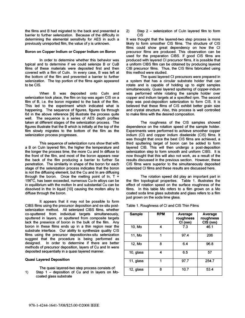
The quasi layered CI precursors were prepared in a system that has a circular substrate holder that can rotate and is capable of holding up to eight samples simultaneously. Quasi layered sputtering of copper-indium was performed while rotating the sample holder over copper and indium targets at a specified rpm. The second step was post-deposition selenization to form CIS. It is believed that these films of CIS exhibit better grain size and crystal structure. Also, this process is well controlled to make films with the desired composition.
The roughness of the CIS samples showed dependence on the rotation speed of the sample holder. Experiments were performed to achieve smoother copper indium (CI) and copper indium diselenide (CIS) films. It was thought that once the best CIS films are achieved, a third sputtering target of boron can be added to form layered CIB. This will then undergo a post-deposition selenization step to form smooth and uniform CIBS. It is now thought that this will also not work, as a result of the results discussed in the previous section. However, these CIS films were superior to the simultaneously deposited selenized CI films and these results are discussed here.
The rotation speed did play an important part in the film topological properties. Table 1. illustrates the effect of rotation speed on the surface roughness of the films. In this table Mo refers to a film grown on a Mo coated soda lime glass substrate and glass refers to a film just grown on the soda lime glass.
Table 1. Roughness of CI and CIS Thin Films
Sample RPM Average Average roughness roughness
CI (nm) CIS (nm) 10, Mo 4 7.3 46.1
11, Mo 1 97.4 206
12, Mo 8 6.4 96.8
10, glass 4 6.5 57
11, glass 1 97.7 254.7
12, glass 8 10.7 53.4

It can be seen that the selenized films are rougher than the precursor films and that a rotation speed of either 4 or 8 rpm is the best.
These films were selenized using the same process as for the simultaneously or individually deposited films. The results here were more promising than the previous results. AES again showed results as expected for both the precursor films and the selenized films. In order to determine if we are creating CIS, XRD measurements were performed. Fig. 1 is an XRD analysis of sample 10 in the above table. It can be seen that the material is polycrystalline in nature.
160000
140000
120000
~ 100000
'iii 80000 j 60000
40000
20000
o 25
Ex-81tu Selenlzed Layered Culn
Mo
CIS - CIS (ll2) (204)
(220)-CIS "''' t: (312)_CIS _CIS CIS _
I (008) (316) (228)
U~ Jl (400)-(332) (424)----;:
35 45 55 65 75 85
28 (Degrees)
Fig 1. An XRD spectrum for a CIS film grown using the quasi layered technique, indicating the grown film matched the spectrum from known CIS.
The XRD peaks are all at the appropriate angle and of the appropriate peak height when compared with the powder diffraction files corresponding to a form of CulnSe2. Although peaks observed from the co-sputtered materials were at the correct value of 28, the relative magnitudes did not match a single powder diffraction file as well, indicating that these quasi-layered CIS films are probably more ordered and of a single phase. In fact, a look at Fig. 2 shows that although the speed of rotation had an effect on surface texture, the films were still CIS. In this figure it can be seen that the XRD spectra for the three runs are essentially identical. In this figure the largest peaks are due to the Mo film on the substrate, the remaining films are CIS.
978-1-4244-1641-7/08/$25.00 ©2008 IEEE
160000
140000
,120000
§100000
180000
~ 60000
40000
-Rml0 -Rmll -Rm12
20000 1 A.. A
O~'~ ~~~~~~~~~~~~ 25 35 45 55 65 75 85
Fig. 2. XRD spectra for three quasi layered films deposited at different rotation rates. Peak assignments are identical to those in Fig. 1.
The bandgap of the material is another measurement that can help determine the quality of the film. Fig. 3 is a Tauc plot for sample 16 which was fabricated under identical conditions to sample 10. The reason for the change is that the Tauc bandgap must be measured on a glass substrate in order to get the optical transmission. The result shows that the material is a direct bandgap material with Eg = 0.95 eV.
8000
7000
S 6000
~ 5000
~4000 ~3000 ,!. 2000
1000
o o
Ex-Situ Selenized Layered Culn
",.r-/'
/ /
/ I I 1 2 3 4
hll(eV)
--5 6 7
Fig. 3. A Tauc bandgap plot of a quasi layered film plotted vs (ahu) 112 indicating that the material is a direct bandgap material with a bandgap of 0.95 eV.
The quasi layered material all exhibited similar results with the measured bandgaps ranging from 0.95 eV to 0.97 eV. Thus, the XRD results and the optical bandgap results were all consistent for the quasi layered films. In order to determine if we truly have CIS films, Raman spectroscopy measurements were also performed on a typical sample, see Fig. 4.

Raman Scattering: Quasi Layered CulnSez 33.8 ,..----,..----,-----,---------,
33.75
t> 33.7 ';J 5 33.65
E 33.6
33.55
33.5 +----+----+----+--------1 125 175 225
Wavenumber (cm'l)
275 325
Fig. 4. Raman scattering spectrum from a quasi layered CulnSe2 thin film.
It can be seen that the Raman peak, though small, is at a wavenumber of 174 cm,1, the expected value for the A1 phonon in a CIS film [11]. Thus, all the results, including AES indicate that the ex-situ selenization of quasi layered films is successful in producing good CIS films. As a consequence of the difficulty in pot deposition selenization of previous films, it was decided not to pursue CIBS using the quasi layered technique described in this section. Instead, it was decided to deposit Cu and In or Cu, In and B in a selenium vapor. The results of this experiment are described in the next section.
IN-SITU SELENIZATION DEPOSITION
Initially, in order to determine if the in-situ selenization method would work, a CU.45ln.55 target was deposited in a vacuum in which Se vapor was present. The Se was vaporized from a stainless steel can which had a small aperture and was pointed at the heated rotating substrate. The initial results on Culn deposition were promising. An AES depth profile of a film grown in this manner is shown in Fig. 5.
AES: In-Sltu Selenlzed Culn
_60,---------------, ~
~50+;=--a-----------~ o i 40 +-I\-I-'~'-b'~:I_"Ic_::__=_''___,,;_=_ ___ __...:--~ ~ ~ 30+--------------~ c o u 20+---~~~~~~~~~~-_1 u 's 10 P'---------------_1 ~
O+-----~------~------~----~ o 10 20
Sputter Cycle 30 40
~cu -In -Se
Fig. 5. Auger depth profile of a film fabricated by sputtering a CU.45In.55 target in a selenium vapor.
978-1-4244-1641-7/08/$25.00 ©2008 IEEE
It can be seen that, although the system is noisy, the materials are quite uniform throughout the film. It should also be noted, that the Cu appears to be at a lower atomic percentage than expected. Even with a different sensitivity for the elements, the Cu content would still be below what was observed for the ex-situ selenized Culn films from the same target. Thus, one would expect that other measurements would indicate that the film is CIS with excess In, and that CuxSe would not be present.
This is confirmed in Fig. 6 which is a Raman spectrum of this film. It can be seen that a peak in the correct vicinity of 170 - 190 cm,1 does exist. The identifying labels on the graph indicate the range of this broad peak. Since our other measurements indicate that we have a CIS film forming, the width of the peak could be due to the fact that the film has an excess of In. However, no peak is observed at 255 cm,1 indicating that CU2,xSe is not present [12] and the Raman peak drops off much before a peak representing Se, which is at 235 cm,1 [13], would be observed.
Raman Scattering: In-Situ Selenized Culn
34
33.9
~ 33.8 III j 33.7 c - 33.6
33.5
33.4
50 150 250 350 450
Wavenumber (cm'l)
Fig. 6. Raman scattering spectrum from an in-situ CIS thin film.
The sample was subjected to further testing to try to understand the fabrication process. Fig. 7 illustrates the Tauc bandgap measurement which is not as clear as is the same plot for the quasi layered, see Fig. 3. The bandgap is calculated to be 0.85 eV, which is also somewhat low.

4500 4000
to! 3500 i' 3000 ~ 2500
S'-' 2000 j 1500 ,!. 1000
500 o
o
In-Situ Selenized Culn
AA .M/' .".rJVu,", ~ r
I I I Eg = 0.85 eV
I 2 3 4 5
hll(eV)
Fig. 7. A Tauc bandgap plot of an in-situ CIS film plotted vs (ahu) 112 indicating that the material is a direct bandgap material with a bandgap of 0.85 eV.
With the reasonable success experienced with insitu selenized CIS the next step was to attempt to grow a CuBSe2 thin film by sputtering a CU3B2 target in the selenium vapor. The film was grown at a temperature of 5000 C which was expected to cause a reaction of Cu, B and Se at the substrate surface. The results shown below were not as expected. The first measurement made was that of the Tauc bandgap. Although there is a trail off at lower energy, the straight line portion of the curve is quite evident and yields a bandgap of 3.03 eV. This result is encouraging since the predicted bandgap for CuBSe2 was 3.17 eV [6].
8000
7000
S 6000
~ 5000 ~ 4000
to! ~ 3000 ..c:I ,!. 2000
1000
o
/"
o
In Situ Selenlzed CuB
~ r /
/I ~ /
/ Eg=3.03eV
/ 2 4 6 8
hll(eV)
Fig. 7. A Tauc bandgap plot of an in-situ CBS film plotted vs (ahu) 112 indicating that the material is a direct bandgap material with a bandgap of 3.03 eV.
However, the Raman spectrum for this film was less encouraging. The peak near 174 cm- 1 has disappeared and the new peak at around 250 cm- 1 is now present, see Fig. 8. This indicates that the film is not CBS, but is probably selenized Cu. Unfortunately, no AES was possible to measure on this film because it was too insulating and no useful data could be obtained. XRD was performed on this film and the results were inconclusive in
978-1-4244-1641-7/08/$25.00 ©2008 IEEE
that none of the peaks aligned with any of the powder diffraction files of any of the expected materials.
33.95
33.85
a- 33.75
! 33.65
~ 33.55
33.45
33.35
Raman Scattering: In-Situ Selenized CuB
33.25 -t---t--t--t--r------1f-----t----t----i
100 150 200 250 300 350 400 450 500
Wavenumber (cm- 1)
Fig. 8. Raman scattering spectrum from an in-situ, expected, CBS thin film.
The second attempt at creating a CBS film using the in-situ technique was a failure. The process created a dangerous level of H2Se. Since this had never been a problem before this result was quite unexpected, and initially unexplainable. It was not known at first if the problem was really H2Se until an RGA was placed on the system and its presence was confirmed. The only difference between this run and all the others is that Se leaked from our vaporization cell and accumulated at the bottom of the vacuum system in a "cake" of what we assumed was Se.
After reviewing more selenium chemistry literature [14], it appears that B2Se3 in contact with water is the most likely source of H2Se. What is strange is how long the presence persists, implying that H2Se generation is slow. A search of the literature shows that it is possible that B2Se3 is being formed [14]. A phase diagram shown in this paper indicates that there is a particularly stable, low-melting (90 0 C) azeotrope that consists of 90% Se and 10% B2Se3.
Our deposition took place under conditions of excess Se, and any B2Se3 that formed may have phased out with Se in this proportion on cool down. The Se "cake" may be this mixture. In this case, H2Se release would be slow because water vapor has to diffuse through a large amount of Se to get to the B2Se3 that's dispersed throughout, and the H2Se that is formed has to diffuse back out through that same Se.
The film created during this run was visibly different from the film illustrated above and was not analyzed. It was thought that this film was very Se deficient. Before any further depositions are made, the system must be completely cleaned and moved to a new specially vented area for safety considerations.
CONCLUSIONS
The fabrication of CulnBSe2 appears to be a very difficult task. In fact, it may not be possible to create this material using the technique of vacuum deposition. Several attempts to deposit such films and post selenize them have been unsuccessful. In addition, deposition of the materials in a Se vapor may not work either.
It is possible that the films produced in vacuum and post selenized may be annealed at high temperature in order to facilitate the needed chemical reactions. This is one avenue that remains to be explored. Another technique which may possible work better is the in-situ selenization of the depositing films in a Se vapor provided by a selenium cracker [15]. In this case, atomic Se would be available for the reaction. A thorough study of the chemical path of reaction must be carried out before the expense of such a cracker can be justified.
If the CulnBSe2 material can be fabricated, it may be necessary to use the solvothermal technique discussed elsewhere in these proceedings [16].
ACKNOWLEDGMENT
This work was supported by the U.S. Department of Energy Office of Science (Grant No. DE-FG02-06ER64235) and the Nebraska Research Initiative Program.
REFERENCES
[1] Miguel A. Contreras, et. aI., " Diode characteristics in state-of-the-art ZnO/CdS/Cu(ln1_xGax)Se2 solar cells", Prog. Photovolt: Res. Appl. 13,2005, pp.209-216.
[2] Stephen J. Fonash, Solar Cell Device Physics, Academic Press, 1981, p. 78.
[3] Kasturi Lal Chopra and Suhit Ranjan Das, Thin Film Solar Cells, Plenum Press, 1983, p. 321.
[4] C. J. Huang, et. aI., "Formation of CulnSe2 thin films on flexible substrates by electrodeposition (ED) technique", Solar Energy Mtrls. Solar Cells 82, 2004, pp. 553-565.
[5] http://www.nrel.gov/news/press/2008/574.html?print
[6] Natale J. lanno, et. aI., "Copper-indium-borondiselenide absorber materials," Mat. Res. Soc. Symp. Proc. 1012 (2007) 1012-T03-21 - 27.
[7] C. A. Kamler,et. aI., "Thin Films Formed by Selenization of CulnxB1-x Precursors in Se Vapor," to be published in Solar Energy Materials and Solar Cells.
[8] A. V. Mudryi, e. aI., "Optical Characterization of HighQuality CulnSe2 Thin Films Synthesised by Two-Stage Selenization Process," Thin Solid Films 431-432, 2003,
978-1-4244-1641-7/08/$25.00 ©2008 IEEE
pp. 193-196.
[9] R. Caballero and C. Guillen, "Optical and Electrical Properties of Culn1- xGa xSe2 Thin Films Obtained by Selenization of Sequentially Evaporated Metallic Layers," Thin Solid Films 431-432, 2003, pp. 200-204.
[10] N. Orbey, et. aI., "Copper Indium Alloy Transformations", J. Phase Equil. 21, 2000, pp. 509-513.
[11] C. Rincon and F.J. Ramirez, "Lattice vibrations of CulnSe2 and CuGaSe2 by Raman microspectrometry", J. Appl. Phys. 72,1992, pp. 4321-4324.
[12] E.P. Zaretskaya, et. aI., "Raman spectroscopy of CulnSe2 thin films prepared by selenization", J. Phys. Chem. Solids 64,2003, pp. 1989-1993.
[13] D. Nesheva, "Raman scattering from semiconductor nanoparticles and superlattices", J. Optoelectronics Adv. Mater. 7, pp. 185-192.
[14] Roger Hillel and Jean Cueilleron, "Etude du selen de bore: B2Se3", Bulletin de la Societe Chemique de France, 1972, pp. 98 -103.
[15] Shogo Ishizuka, et. al. "Preparation of Cu(ln1-xGax)Se2 Thin Films and Solar Cells Using a Se-radical Beam Source", Mat. Res. Soc. Symp. Proc. 1012 (2007) 1012-Y01-01.
[16] Christopher L. Exstrom, et. aI., "Reaction Pathway Insights Into the Solvothermal Preparation of Culn1-xGa xSe2 Nanocrystalline Materials", Proc. PVSC 2008.
Copyright © 2022 FDOKUMEN