experimental validation of high post-yield stiffness dampers for ...

Effect of Defects on the Intrinsic Strength and Stiffness of Graphene
Ardavan Zandiatashbar1†, Gwan-Hyoung Lee2,3†, Sung Joo An2, Sunwoo Lee4, Nithin Mathew1, Mauricio Terrones5,6, Takuya Hayashi6, Catalin R. Picu1*, James Hone2*, and Nikhil Koratkar1,7*
1Department of Mechanical, Aerospace, and Nuclear Engineering, Rensselaer Polytechnic Institute, Troy, New York12180, USA 2Department of Mechanical Engineering, Columbia University, New York, 10027, USA 3Department of Materials Science and Engineering, Yonsei University, Seoul 120-749, Korea. 4Department of Electrical Engineering, Columbia University, New York, NY 10027, USA 5Department of Physics, Department of Chemistry, Department of Materials Science and Engineering and Center for 2-Dimensional and Layered Materials, The Pennsylvania State University, University Park, PA 16802, USA 6Faculty of Engineering and Research Center for Exotic Nanocarbons, Shinshu University, 4-17-1 Wakasato, Nagano, 380-8553, Japan 7Department of Materials Science and Engineering, Rensselaer Polytechnic Institute, Troy, New York 12180, USA † These authors contributed equally to this work. *To whom correspondence should be addressed: RCP ([email protected]), JH ([email protected]) and NK ([email protected]).
It is important both from a fundamental standpoint and for practical applications to
understand how the mechanical properties of graphene are influenced by defects.
Here we report that the 2D modulus of graphene is maintained even at a high
density of sp3-type defects. Moreover, the breaking strength of defective graphene is
only ~14% smaller than its pristine counterpart in the sp3-defect regime. By
contrast, we report a significant drop in the mechanical properties of graphene in
the vacancy-defect regime. We also provide a mapping between the Raman-spectra
of defective graphene and its mechanical properties. This provides a simple, yet non-
destructive methodology to identify graphene samples that are still mechanically
functional. By establishing a relationship between the type and density of defects
and the mechanical properties of graphene, this work provides important basic
information for the rational design of composites and other systems utilizing the
high modulus and strength of graphene.

INTRODUCTION
Pristine (i.e. defect-free) graphene exhibits ultra-high modulus and unsurpassed
strength1. Atomic force microscope (AFM)-based nanoindentation experiments
performed on defect-free graphene has yielded a Young’s modulus of ~1 TPa and tensile
strength of over 100 GPa2-3, as theoretically predicted1. However, for various practical
applications of graphene, such as composites4–6, chemical sensors7,8, ultra-capacitors9,
transparent electrodes10,11, photo-voltaic cells12, and bio-devices13–15, the emergence of
defects in the graphene lattice is inevitable either due to the production process used16–18
or due to the environmental and operating conditions under which the graphene device
operates19–23. In addition, in bio-devices and DNA decorated graphene13–15, the presence
of defects is essential for the desired functionality. Defect engineering of graphene is also
used in nano-electronics for opening a band gap24, DNA-sequencing through nanopores25,
and selective molecular sieving through the nanopores of suspended graphene26. Given
that defects are ubiquitous in the operational environment of graphene devices, it is
important to understand how the defectiveness of graphene impacts its elastic properties
and intrinsic strength.
Computational work has investigated the mechanical properties of graphene in the
presence of vacancies27–31, bond reconstruction32–35, and functional groups36. Several
studies have also shown the formation and structural evolution of defects in graphene
using both experimental37,38 and theoretical tools39–42. However, on the experimental side,
there has been virtually no measurement of how the density and type of defects affect the
mechanical properties of graphene. Even though the elastic stiffness of graphene oxide,
which represents a highly defective state of graphene, was reported by AFM observation

of shape changes in graphene oxide membranes43, only its modulus was provided,
without measurement of breaking strength.
In this study, we use a modified oxygen-plasma technique to induce defects in
pristine graphene in a controlled manner. We utilize Raman spectroscopy and aberration
corrected transmission electron microscopy to characterize the defects. We then use
atomic-force-microscopy nanoindentation to experimentally quantify the stiffness and
strength of defective graphene, and use finite element modeling and molecular
simulations to understand this behavior. Our results indicate that graphene sheets with
defects are more rugged and structurally robust than what was previously thought. While
thermal and electrical transport in graphene is very sensitive to disruptions in the sp2
bonding network, its mechanical properties are far more tolerant of defects and
imperfections
RESULTS
Sample preparation
In our experimental study, a 1×1 cm2 array of circular wells with diameters
ranging from 0.5 μm to 5 μm was patterned on a Si chip with a 300 nm SiO2 epilayer, by
photolithography and reactive ion etching. Graphene was mechanically exfoliated on the
patterned substrate2,21 to create suspended membranes. Monolayer graphene flakes were
identified by optical microscopy and Raman spectroscopy. Elastic stiffness and breaking
force were measured by atomic force microscopy (AFM) nanoindentation with a
diamond AFM tip, as shown in the schematic of Fig. 1a. Figure 1b shows optical
micrographs of monolayer and bilayer graphene sheets covering distinct holes of

different diameters. Prior to the indentation testing, non-contact mode AFM imaging was
used to confirm that the graphene sheets are well suspended as shown in Fig. 1c.
Introduction of defects
A tabletop oxygen plasma etcher was used to induce defects in the suspended
graphene sheets (See Methods and Supporting Information). Weak oxidation by ion
bombardment, oxygen plasma or ultraviolet irradiation has been used to etch graphene or
generate defects26, 44–46. Compared to these techniques, the etch rate of graphene in the
oxygen plasma is fast: ~ 9 layers per minute at a chamber pressure of ~215 mTorr. To
shield the graphene from direct exposure to the plasma, the graphene-deposited Si chips
were placed upside down in the plasma chamber between two glass slides (see
Supplementary Fig. 1a). This reduced the etch rate by a factor of ~30 (Supplementary
Fig. 1b and c), and allowed the suspended graphene to survive without breaking or
collapse even after plasma exposure of 55 s.
Raman spectroscopy
To quantitatively examine the type and density of defects in the graphene sheets,
the graphene was characterized using Raman spectroscopy47,48. Figure 2a shows the
evolution of the Raman spectrum with increasing plasma time for a typical monolayer
graphene supported on the SiO2/Si substrate, which was repeatedly exposed to oxygen
plasma with 3-second periods and then characterized by Raman spectroscopy after each
plasma exposure dose. As expected, the D and D' peaks, indicative of disorder, begin to
rise and become more prominent with increased plasma exposure time, while conversely

the 2D peak weakens and broadens49. Interestingly, when Raman spectra were obtained
from the suspended graphene, the D peak appeared at shorter exposure times and the
peak intensity ratios are different from those in the supported one as shown in Fig. 2b.
The peak intensity ratios of D to G peaks (I(D)/I(G)), 2D to G peaks (I(2D)/I(G)), and D
to D' peaks (I(D)/I(D')) for supported graphene are plotted in Fig. 2c. It is evident that
I(D)/I(G) increases with the increase of plasma time until it reaches maximum value of
~4 at ~27 s and then decreases. On the other hand, I(2D)/I(G) exhibited a slow decrease
at the initial stage and then an abrupt decrease around 20 s; such behaviors are also
observed in the defective graphene induced by other etching techniques45–49. Even though
the Raman spectra (Fig. 2b) and peak intensity ratio (Fig. 2d) of the suspended graphene
shows different values at the same plasma exposure time from those of the supported one,
they follow a similar trend (Supplementary Fig. 2). Note that these differences in Raman
results between supported and suspended graphene sheets may be attributed to the
substrate effect on Raman intensity in the supported graphene48, presence of pre-stress2
and etching of both sides50 in the suspended graphene.
It has been reported by A. Eckmann et al.49 that the I(D)/I(D') intensity ratio can
be used to discriminate between sp3-type defects, in which an oxygen atom binds to the
graphene, and vacancy-type defects. Therefore, we categorize the defects49 as being
predominantly sp3-type (partial oxidation, I(D)/I(D') > 7) or predominantly vacancy-type
(I(D)/I(D') < 7) as shown in Figs. 2c-d. Because the crossover between these two regimes
is gradual, the boundary is indicated by the blurred color in Figs. 2c-d. The crossover
region also correlates well to the point at which the I(D)/I(G) intensity ratio achieves a
maximum for both the suspended and supported graphene. Our MD simulation results,

which will be discussed in detail later, also confirmed the similar evolution of sp3-type
and vacancy-type defects with increasing plasma time. To measure the defect density, an
average distance between defects (LD), which is used as top x-axis in Figs. 2c-d, was
calculated using the I(D)/I(G) intensity ratio, as reported46, 48 (See supporting information
for details). Note that for both the supported and suspended graphene, the I(D)/I(G)
intensity ratio increased and reached a maximum at LD ~ 5 nm, then decreased
(Supplementary Fig. 2g). To further characterize the types of defects generated by
oxygen plasma, high resolution AFM imaging was performed with ultra-sharp diamond-
like carbon tip (NT-MDT, NSG01_DLC) as shown in Fig. 3a-c. The membrane appears
as a continuous sheet with no pores before plasma etching (Fig. 3a-b). After 55 s plasma
etching (Fig. 3c), imaging reveals extended defects, i.e. nanopores, that are of the order of
several nm in diameter (indicated by black dots in Fig. 3(b)), as reported elsewhere26,49.
Suspended bilayer graphene sheets also showed a uniform distribution of nanopores
(Supplementary Fig. 4) which confirms the etching of the graphene sheets by the oxygen
plasma treatment.
AFM nanoindentation study
To study the evolution of mechanical properties with defect density, a series of
samples was prepared and each exposed to oxygen plasma for a given time (ranging from
0-55 s), then characterized by Raman spectroscopy. Because of the variability of the
oxygen plasma etching, the absolute etch time is not a reliable measure of the defect
density. Consequently, the Raman parameters of I(D)/I(G) and I(2D)/I(G) were used to
quantify the degree of defectiveness of the graphene sheets. To measure mechanical

properties, the suspended sheets were indented by AFM as reported previously2, using a
diamond AFM tip with a radius of 80 nm. Figure 3d shows typical force vs. displacement
curves for a defective graphene sheet exposed for 30 s. AFM imaging of a defective
graphene sheet after fracture (Fig. 3d, inset), indicates that fracture in the defective
graphene occurs under the tip, as for pristine graphene. The two-dimensional (2D) elastic
modulus is determined by fitting the force vs. displacement response to a quasi-empirical
polynomial form, containing linear and cubic deflection terms, as previously used for
pristine graphene2 (details provided in the Supplementary Information).
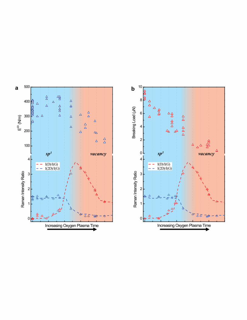
Figure 4a shows the evolution of the 2D modulus (E2D) as a function of the
Raman parameters. Remarkably, E2D remains constant (within experimental uncertainty)
over the entire sp3-type defect region (i.e. when I(D)/I(G) < 1, I(2D)/I(G) > 1 and
I(D)/I(D') > 7), indicating that these defects do not appreciably change the stiffness, even
at a spacing LD of ~5 nm. Once the graphene crosses over into the vacancy-type defect
region (i.e. when I(D)/I(G) >1, I(2D)/I(G) < 1 and I(D)/I(D') < 7), E2D decreases with
increasing defect density, reaching ~30% of the stiffness of the pristine sheet at the
maximum exposure time.
Compared to the elastic stiffness, the breaking load of Fig. 4b shows greater
sensitivity to defects regardless of type. To calculate the breaking strength of defective
graphene from the breaking load, we used the nonlinear finite element method (FEM)
based on ab initio density functional theory calculations (See Supporting Information).
This analysis yields a strength of ~35 N/m for pristine graphene, consistent with previous
measurements3. Because of the highly nonlinear relationship between strength and
breaking load, the ~two-fold decrease in breaking load observed at an I(D)/I(G) ratio of

~ 1.0 corresponds to a decrease in strength of only ~14%, to ~30 N/m (Supplementary
Fig. 3). This is a central finding of our study: graphene can maintain a large fraction of its
pristine strength and stiffness in the presence of a high density of sp3-type defects. These
results can enable the rational design of graphene based composite materials, because one
can now quantify the trade-off that exists between defects (e.g. due to cross-linking or
processing) and mechanical properties (such as 2D modulus and strength). Once the
graphene passes into the vacancy-type region, the linear elastic modulus (and presumably
the higher-order elastic moduli as well) changes. Therefore, the nonlinear FEM technique
cannot be applied in this regime. For a rough estimate, we note that in the linear elastic
approximation, strength varies as (FbE2D)0.5, where Fb is the breaking load2. In this
simple model, the breaking strength at the highest plasma exposure time in our
experiments is roughly ~4 times smaller than that of pristine graphene.
DISCUSSION
The mapping of the mechanical properties of defective graphene (Figure 4a-b) to
their Raman spectra indicate that, for I(D)/I(G)<1 and I(2D)/I(G) >1 (i.e. in the sp3-type
defect regime), the elastic stiffness of defective graphene is not significantly diminished
in comparison to its pristine counterpart. This is surprising, since an I(D)/I(G) ratio of 1 is
generally considered to represent a relatively high state of defectiveness in graphene. For
instance I(D)/I(G) values of ~1.0 are typical of graphene that is synthesized by chemical
or thermal reduction of graphene oxide. Such reduced graphene oxide sheets are known
to offer significantly lower electrical8 and thermal conductivity51 compared to pristine
graphene due to their defective state. By contrast, for mechanical properties, we find that

graphene is capable of tolerating defects and retaining its ultra-high stiffness properties.
As compared to the stiffness, the breaking force (Fig. 4b) of graphene shows greater
sensitivity to defects. Nevertheless, due to the nonlinear elastic behavior of graphene
(Supplementary Fig. 3), the strength of defective graphene is only ~14% smaller than its
pristine counterpart in the sp3-type defect regime. Our results provide a simple, non-
contact and non-destructive approach to quantifying the mechanical properties of
defective graphene samples. This involves measuring the intensities of the Raman D and
2D peaks with respect to the G peak. Using the direct mapping between the Raman
parameters and the measured 2D modulus and breaking load that we report (Figure 4a-b),
it is possible to determine in a quantitative yet non-destructive manner how the
mechanical properties of graphene vary as a function of its defectiveness. This has
important practical implications for the design of a broad range of graphene based
devices such as chemical sensors7,8, ultra-capacitors9, transparent electrodes10,11, photo-
voltaic cells12, bio-devices13–15, nano-electronics24, DNA-sequencing through
nanopores25, and selective molecular sieving through the nanopores of suspended
graphene26.
Aberration corrected high-resolution transmission electron microscopy (AC-
HRTEM) characterization (Figure 5) of the graphene lattice was also carried out at both
low and high oxygen plasma times. Figure 5a is representative of a graphene sheet in the
sp3 defect regime (I(D)/I(G) ~ 0.2 and I(2D)/I(G) ~ 1.5) while figure 5b is typical of a
graphene sample in the vacancy-defect regime (I(D)/I(G) ~ 2.0 and I(2D)/I(G) ~ 0.2).
Both figures 5a-b show presence of polymer residue (associated with the transfer3 onto
the TEM grid). However it is evident that while Figure 5b indicates an abundance of

nano-cavities (i.e. etch pits) in the graphene lattice (representative of the vacancy-defect
regime), Fig. 5a shows a contrasting absence of such cavities. The black dots (circled in
Fig. 5a) are sp3 point defects that correspond to oxygen ad-atoms52. The upper and lower
insets in Fig. 5a show obtained TEM image and the corresponding simulated image of an
oxygen atom attached to sp3 carbon. The settings (Cs: 0.005 mm, Scherzer focus: -53
angstrom, operated at 80 keV) in the simulated TEM image is identical to what was used
in the experimental image. These images confirm that sp3 point defects in the form of
oxygen ad-atoms are generated in the sp3 defect regime, while with increasing plasma
exposure carbon atoms are etched from the lattice resulting in the formation of nano-
cavities or nano-pores in the vacancy-defect regime. Energy dispersive spectroscopy
(EDS) analysis (Supplementary Fig. 6) of the graphene suspended over the holes in the
TEM grid also confirmed a significant increase in the oxygen content at short plasma
times (in the sp3–type defect regime) as compared to pristine graphene.
It should be noted that our AFM-nanoindentation technique reveals only the
spatially averaged mechanical properties of the defective graphene sheet. However a
recent study53 which used topographical atomic force microscopy (AFM) imaging on
wrinkled graphene oxide and wrinkled chemically-reduced graphene oxide sheets
revealed significant heterogeneity in the in-plane modulus of chemically-modified carbon
nanomaterials. The modulus of graphene oxide (GO) was found to vary between 0.42
TPa and 0.11 TPa due to defect concentration or clustering of different functional groups.
They determined the average modulus for GO to be ~0.23 TPa; this is in reasonable
agreement with the samples with the highest plasma exposure (Fig. 4a) that we tested
which showed a modulus of ~0.3 TPa. For chemical vapor deposition grown pristine

graphene, Ref. 53 reports far less spatial heterogeneity in properties with an averaged
modulus of ~0.91 TPa which shows good agreement with our result (~1 TPa) for pristine
graphene (Fig 4a). Another striking observation in Ref. 53 was that the heterogeneities
introduced during synthesis of GO were not removed in chemically reduced graphene
oxide (RGO) with the material still exhibiting significant spatial heterogeneity (the
modulus of RGO varied between ~0.82 TPa and ~0.36 TPa). This is important because
mechanical failure is typically dictated by the weaker (or the more defective) regions.
This is consistent with our results for breaking load (Fig. 4b) which indicate a higher
sensitivity of the failure load to defects as compared to the material modulus.
In addition to the aforementioned experiments and defect characterization studies,
we also performed atomistic modeling using the molecular dynamics (MD) simulator,
LAMMPS (large-scale atomic/molecular massively parallel simulator). The Reactive
Force Field (ReaxFF) potential used in this study is specially trained for simulation of
hydrocarbon oxidation54 and can simulate continuous bond formation and breakage55. In
the simulations, oxygen atoms are placed on both sides of the graphene sheet (Fig. 6a)
and kept stationary during equilibration. The graphene is equilibrated for 2 ps in the
isobaric-isothermal (NPT) ensemble at 300 K and 0 pressure in all directions with a
Nose-Hoover thermostat for temperature control and a time step of 0.2 fs (Fig 6b). Much
longer equilibration periods were run in separate tests to insure that 2 ps would
sufficiently equilibrate the systems under the given conditions. Post-equilibration,
random velocity vectors corresponding to 300 K are assigned to oxygen atoms (Fig. 6c).
Micro-canonical (NVE) ensemble with a time step of 0.2 fs is used to run the simulation
since the local temperature rise due to collision of carbon and oxygen atoms has a vital

role in driving the reactions. Therefore no external heat bath (i.e. thermostat) was used as
in Ref. 56. Note that the oxygen plasma cleaner used in the experiments generates a
cold (or non-thermal) plasma. Since we are simulating cold plasma, the velocity that is
given to the oxygen atoms is considered to be equivalent to room temperature (300 K).
The simulation ends after the oxygen has completely etched away the entire carbon
network (Fig. 6d).
We considered four different numbers of oxygen atoms: 750, 1000, 1500 and
4500 in the simulations corresponding to varying oxygen pressures. These simulations
are representative and have been selected from a large pool of runs of stochastically
similar systems. The number of carbon atoms in the graphene sheet was kept constant at
1500. In the supplementary information we plot the number of carbon atoms removed
from the graphene lattice by the oxygen plasma and the number of chemisorbed oxygen
atoms normalized by the total number of carbon atoms in the graphene lattice as a
function of the plasma time. The result (Supplementary Fig. 5) resembles a cumulative
Weibull distribution with three distinct regimes: (1) incubation period, (2) an
intermediate regime and (3) a terminal regime. The incubation period corresponds to
before the chemisorption of oxygen sets in. The intermediate regime is when oxygen
atoms attach to the graphene lattice and generate defects. The terminal regime
corresponds to fast growth, percolation and coalescence of defects resulting in large
cavities in the lattice. During the terminal regime the number of carbon atoms removed
from the graphene lattice increases sharply culminating in the complete breakup of the
graphene structure. The structures formed and evolved during the intermediate regime are
of interest for this study.

Let us consider the case of 1000 oxygen atoms in the simulation. For this case, the
incubation period ends and intermediate regime begins at ~200 ps, while the terminal
region begins after ~320 ps of plasma time (Supplementary Fig. 5). The time period from
200 ps to 350 ps was divided into ten equal sub-intervals and ten structures corresponding
to the end of each time interval and the initial graphene structure at 200 ps were selected
for uniaxial tensile testing. The tensile loading simulations were performed at 300 K
using a Nose-Hoover thermostat for temperature control and a time step of 0.2 fs while
maintaining zero pressure in the lateral (i.e. armchair) direction. The calculated 2D elastic
stiffness and ultimate strength for these eleven structures are plotted in Fig. 6e. The
results mirror our experimental observations in that the elastic stiffness does not degrade
significantly up to ~310 ps (corresponding to sp3-defect regime), after which we see a
rapid loss in elastic stiffness in the terminal regime, which corresponds to the vacancy-
defect regime of Fig. 4a. The MD simulations qualitatively capture the experimental
observations and shed light onto how defects influence the mechanical properties of
graphene. The strength predictions (in Fig. 6e) show a gradual decrease in strength up to
~310 ps (in the sp3-defect regime) followed by a much more precipitous drop in the
vacancy-defect regime (at 350 ps) which is also consistent with our experimental
observations. It should be noted that the predicted 2D modulus for pristine graphene is
~420 N/m (corresponds to ~1.2 TPa Young’s modulus) which overestimates the modulus
of pristine graphene (~1 TPa). This is because the ReaxFF potential that was used in our
study is not fully optimized (calibrated) for mechanical properties prediction. The choice
of the ReaxFF potential in our work was dictated by its ability to simulate hydrocarbon
oxidation as well as the continuous formation and breakage of bonds.

In order to explain why the elastic stiffness of the graphene sheet shows lower
sensitivity to defects as compared to its breaking strength we considered the structure of
the chemisorbed oxygen and the processes of carbon atom removal from the graphene
lattice. During the simulation, carbonyl groups are initially formed due to the
chemisorption of oxygen (Fig. 6f). Increasing numbers of chemisorbed oxygen atoms
then result in the formation of epoxide and ether groups. This functionalization of the
graphene lattice with carbonyl, epoxide, and ether groups involves rupture of some C-C
bonds which introduces discontinuities in the graphene lattice as indicated in Fig. 6f.
Breaking of C-C bonds lowers the strength of the graphene sheet which explains why the
strength gradually drops in the experiments and in the simulations with the chemisorption
of oxygen functional groups. Unlike strength, localized disruptions to the carbon bonding
network does not significantly lower the elastic stiffness of the two-dimensional graphene
structure. However, the situation changes beyond 320.6 ps of plasma time when
significant numbers of carbon atoms are physically removed (Fig. 6f) from the graphene
lattice. More importantly, as the density of defects increases (332.6 ps in Fig. 6g)
adjacent defects coalesce to form bigger voids (338.6 ps in Fig. 6g). At this stage large
numbers of carbon atoms are rapidly removed from the graphene lattice which results in a
precipitous drop in elastic stiffness and strength as the graphene structure breaks apart.
The formation of nano-cavities in the graphene lattice in the vacancy-defect regime is
also corroborated by AC-HRTEM imaging of the graphene sheet (as shown in Fig. 5).
To summarize, over the entire sp3-type defect region, the 2D modulus and
strength of graphene is relatively insensitive to defects, even at a spacing LD of ~5 nm.
This has important implications for design of graphene based composite materials since it

indicates that graphene can be covalently bonded to polymer matrices without sacrificing
its reinforcing abilities. Only in the vacancy defect regime, when the plasma begins to
etch the graphene sheet and remove large numbers of carbon atoms, does the modulus
and strength of graphene begins to degrade significantly. The direct mapping between the
Raman signature of defective graphene and its mechanical properties that we provide
allows for a simple and non-destructive methodology to predict the 2D modulus and
breaking strength of defective graphene without actually testing it. These results could
enable the rational design of graphene composites as well as mechanically-stable
graphene membranes for a variety of applications.
Methods
Sample Preparation. To fabricate array of holes with various diameters of 0.5 ~ 5 μm, a
Si wafer with 300 nm SiO2 capping was patterned by conventional photolithography and
reactive ion etching. The depth of hole is ~ 1 μm for indentation test. The graphene sheets
were deposited on the patterned substrate by the well-established Scotch tape method2,18.
A bench-top radio frequency oxygen plasma cleaner (Plasma Etch Inc., PE-50 XL,
100W) was utilized for introducing defects in graphene. To increase the controllability of
defect generation, the chip was flipped and placed upside down on two carefully cleaned
glass slides, in the oxygen plasma chamber (Supplementary Fig. 1). For the HRTEM
imaging, the pristine samples were transferred to a TEM grid using poly (methyl
methacrylate) (PMMA) transfer method3. After removal of PMMA through annealing,
the samples were then exposed to oxygen plasma irradiation in the same manner.
Characterization of Defects: The type and density of defects in the graphene sheets
were characterized using Raman spectroscopy (Renishaw, inVia with 532 nm wavelength
laser and 0.7 �m spot size). HRTEM instruments (JEOL, JEM-2100F with double Cs
correctors, operated at 80 keV and JEOL, JED-2300T) were used for high-resolution
imaging and EDS, respectively. TEM image simulation of oxygen ad-atom (an oxygen

atom attached to sp3 carbon) was conducted using settings (Cs: 0.005 mm, Scherzer
focus: -53 angstrom, operated at 80 keV) that are identical to that used in the experiments
to acquire the images.
AFM Nanoindentation. The precise nanoindentation on the suspended graphene was
performed using AFM (Park Systems, XE-100). Before each indentation, the samples
were scanned in non-contact mode to find graphene sheets fully covering a hole. After
scanning, the diamond AFM tip (MicroStar Tech) was centered in the middle of the
circular hole. Mechanical testing was performed using force-displacement mode. When
non-trivial hysteresis was observed (presumably due to slippage of the graphene on the
substrate), their corresponding data were discarded. The non-linear force vs.
displacement curves obtained from the AFM nanoindentation tests were used to
quantitatively determine the elastic stiffness and breaking load of defective graphene
following the model described in Ref. 2 and 3.
Molecular Dynamics (MD) Simulations. LAMMPS (Large-scale Atomic/Molecular
Massively Parallel Simulator) was used for MD simulations as it has been extensively
tested and successfully used for modeling solid, liquid, and gaseous systems using
different force fields and boundary conditions. For the purpose of atomistic modeling of
graphene and its chemical reactions with oxygen Reactive Force Field (ReaxFF) potential
was used. The ReaxFF used in this study is specially trained for simulation of hydro-
carbon oxidation54 and is able to bridge the gap between quantum chemical and empirical
force field based computational chemical methods54,55. In the initial state, the oxygen
atoms are placed not closer than 1 nm from the graphene sheet surface. This distance is
intentionally selected to be larger than the nearest neighbor cutoff distance (0.45 nm) to
avoid initial interactions between oxygen atoms and the graphene sheet. To remove the
in-plane pressure from graphene (pressure components along x and y directions),
graphene is equilibrated for 2 ps in the isobaric-isothermal (NPT) ensemble at 300 K and
0 pressure in all directions with a Nose-Hoover thermostat (Tstart, Tstop of 300 K and
Tdamp of 10 K) for temperature control and a time step of 0.2 fs. After equilibration,
random velocity vectors corresponding to 300 K are assigned to the oxygen atoms. The
carbon atoms already have velocities corresponding to 300 K. This is followed by

running the simulation in the micro-canonical (NVE) ensemble with a time step of 0.2 fs
and without coupling the system to an external heat bath using a thermostat56. Additional
information is provided in the supplementary information.
References
1. Geim, A. K. & Novoselov, K. S. The rise of graphene. Nature Mater. 6, 183–191 (2007).
2. Lee, C., Wei, X., Kysar, J. W. & Hone, J. Measurement of the elastic properties and intrinsic strength of monolayer graphene. Science 321, 385–388 (2008).
3. Lee, G. H. et al. High strength chemical-vapor-deposited graphene and grain boundaries. Science 340, 1073-1076 (2013).
4. Stankovich, S. et al. Graphene-based composite materials. Nature 442, 282–286 (2006).
5. Rafiee, M. A. et al. Enhanced mechanical properties of nanocomposites at low graphene content. ACS Nano 3, 1–17 (2009).
6. Zandiatashbar, A., Picu, C. R. & Koratkar, N. Control of epoxy creep using graphene. Small 8, 1676–1682 (2012).
7. Schedin, F. et al. Detection of individual gas molecules adsorbed on graphene. Nature Mater. 6, 652–655 (2007).
8. Yavari, F., Castillo, E., Gullapalli, H., Ajayan, P. M. & Koratkar, N. High sensitivity detection of NO2 and NH3 in air using chemical vapor deposition grown graphene. Appl. Phys. Lett. 100, 203120 (2012).
9. Stoller, M. D., Park, S., Zhu, Y., An, J. & Ruoff, R. S. Graphene-based ultracapacitors. Nano Lett. 8, 3498–502 (2008).
10. Yin, Z. et al. Electrochemical deposition of ZnO nanorods on transparent reduced graphene oxide electrodes for hybrid solar cells. Small 6, 307–312 (2010).
11. Gomez De Arco, L. et al. Continuous, highly flexible, and transparent graphene films by chemical vapor deposition for organic photovoltaics. ACS Nano 4, 2865–2673 (2010).
12. Wang, X., Zhi, L. & Müllen, K. Transparent, conductive graphene electrodes for dye-sensitized solar cells. Nano Lett. 8, 323–327 (2008).

13. Ang, P. K., Chen, W., Wee, A. T. S. & Loh, K. P. Solution-gated epitaxial graphene as pH sensor. J. Amer. Chem. Soc. 130, 14392–14393 (2008).
14. Cohen-Karni, T., Qing, Q., Li, Q., Fang, Y. & Lieber, C. M. Graphene and nanowire transistors for cellular interfaces and electrical recording. Nano Lett. 10, 1098–1102 (2010).
15. Dong, X., Shi, Y., Huang, W., Chen, P. & Li, L.-J. Electrical detection of DNA hybridization with single-base specificity using transistors based on CVD-grown graphene sheets. Adv. Mater. 22, 1649–1653 (2010).
16. McAllister, M. J. et al. Single sheet functionalized graphene by oxidation and thermal expansion of graphite. Chem. Mater. 19, 4396–4404 (2007).
17. Schniepp, H. C. et al. Functionalized single graphene sheets derived from splitting graphite oxide. J. Phys. Chem. B. 110, 8535–8539 (2006).
18. Stankovich, S. et al. Stable aqueous dispersions of graphitic nanoplatelets via the reduction of exfoliated graphite oxide in the presence of poly(sodium 4-styrenesulfonate). J. Mater. Chem. 16, 155 (2006).
19. Kim, K. S. et al. Large-scale pattern growth of graphene films for stretchable transparent electrodes. Nature 457, 706–710 (2009).
20. Bae, S. et al. Roll-to-roll production of 30-inch graphene films for transparent electrodes. Nature Nanotechnol. 5, 574–578 (2010).
21. Novoselov, K. S. et al. Two-dimensional atomic crystals. Proc. Natl. Acad. Sci. 102, 10451–10453 (2005).
22. Park, S. & Ruoff, R. S. Chemical methods for the production of graphenes. Nature Nanotechnol. 4, 217–224 (2009).
23. Kittel, C. Introduction to Solid State Physics. 704 (John Wiley & Sons: 2004).
24. Nourbakhsh, A. et al. Bandgap opening in oxygen plasma-treated graphene. Nanotechnol. 21, 435203 (2010).
25. Garaj, S. et al. Graphene as a subnanometre trans-electrode membrane. Nature 467, 190–193 (2010).
26. Koenig, S. P., Wang, L., Pellegrino, J. & Bunch, J. S. Selective molecular sieving through porous graphene. Nature Nanotechnol. 7, 728-732 (2012).
27. Fedorov, A. S. et al. Mobility of vacancies under deformation and their effect on the elastic properties of graphene. J. Exp. Theor. Phys. 112, 820–824 (2011).
28. Tapia, A., Peón-Escalante, R., Villanueva, C. & Avilés, F. Influence of vacancies on the elastic properties of a graphene sheet. Comp. Marter. Sci. 55, 255–262 (2012).
29. Xiao, J. R., Staniszewski, J. & Gillespie, J. W. Tensile behaviors of graphene sheets and carbon nanotubes with multiple Stone–Wales defects. Mater. Sci. Eng. A 527, 715–723 (2010).
30. Paci, J. T., Belytschko, T. & Schatz, G. C. Computational studies of the structure, behavior upon heating and mechanical properties of graphite oxide. J. Phys. Chem. C 111, 18099-18111 (2007).
31. Khare, R. et al. Coupled quantum mechanical/molecular mechanical modeling of the fracture of defective carbon nanotubes and graphene sheets. Phys. Rev. B 75, 1–12 (2007).
32. Dettori, R., Cadelano, E. & Colombo, L. Elastic fields and moduli in defected graphene. J. Phys.- Condens. Matter 24, 104020 (2012).
33. Wang, M. C., Yan, C., Ma, L., Hu, N. & Chen, M. W. Effect of defects on fracture strength of graphene sheets. Comp. Mater. Sci. 54, 236–239 (2012).
34. Xiao, J. R., Staniszewski, J. & Gillespie, J. W. Fracture and progressive failure of defective graphene sheets and carbon nanotubes. Compos. Struct. 88, 602–609 (2009).
35. Ansari, R., Ajori, S. & Motevalli, B. Mechanical properties of defective single-layered graphene sheets via molecular dynamics simulation. Superlattice. Microst. 51, 274–289 (2012).
36. Pei, Q. X., Zhang, Y. W. & Shenoy, V. B. A molecular dynamics study of the mechanical properties of hydrogen functionalized graphene. Carbon 48, 898–904 (2010).
37. Meyer, J. C. et al. Direct imaging of lattice atoms and topological defects in graphene membranes. Nano Lett. 8, 3582–3586 (2008).
38. Banhart, F., Kotakoski, J. & Krasheninnikov, A. V. Structural defects in graphene. ACS Nano 5, 26–41 (2011).
39. Stone, A. J. & Wales, D. J. Theoretical studies of icosahedral C60 and some related species. Chem. Phys. Lett. 128, 501–503 (1986).
40. Bonilla, L. & Carpio, A. Graphene simulation: Theory of Defect Dynamics in Graphene. chap. 9, 167-182 (In Tech: 2011)

41. Bagri, A. et al. Structural evolution during the reduction of chemically derived graphene oxide. Nature Chem. 2, 581–587 (2010).
42. Bagri, A., Grantab, R., Medhekar, N. V. & Shenoy, V. B. Stability and formation mechanisms of carbonyl- and hydroxyl-decorated holes in graphene oxide. J. Phys. Chem. C 114, 12053–12061 (2010).
43. Suk, J. W., Piner, R. D., An, J. & Ruoff, R. S. Mechanical properties of monolayer graphene oxide. ACS Nano 4, 6557–6564 (2010).
44. Kim, D. C. et al. The structural and electrical evolution of graphene by oxygen plasma-induced disorder. Nanotechnol. 20, 375703 (2009).
45. Cancado, L. G. et al. Quantifying defects in graphene via Raman spectroscopy at different excitation energies. Nano Lett. 11, 3190–3196 (2011).
46. Lucchese, M. M. et al. Quantifying ion-induced defects and Raman relaxation length in graphene. Carbon 48, 1592–1597 (2010).
47. Dresselhaus, M. S., Jorio, A., Souza Filho, G. & Saito, R. Defect characterization in graphene and carbon nanotubes using Raman spectroscopy. Philos. T. Roy. Soc. A 368, 5355–77 (2010).
48. Araujo, P. T., Terrones, M. & Dresselhaus, M. S. Defects and impurities in graphene-like materials. Mater. Today 15, 98–109 (2012).
49. Eckmann, A. et al. Probing the nature of defects in graphene by Raman spectroscopy. Nano Lett. 12, 3925–3930 (2012).
50. Mathew, S. et al. Mega-electron-volt proton irradiation on supported and suspended graphene: A Raman spectroscopic layer dependent study. J. App. Phys. 110, 084309 (2011).
51. Balandin, A. A. Thermal properties of graphene and nanostructured carbon materials. Nature Mater. 10, 569–581 (2011).
52. Gómez-Navarro, C. et al Atomic structure of reduced graphene oxide. Nano Lett. 10, 1144–1148 (2010).
53. Kunz, D. A. et al. Space-resolved in-plane moduli of graphene oxide and chemically derived graphene applying a simple wrinkling procedure. Adv. Mater. 25, 1337–1341 (2013).
54. Chenoweth, K., Van Duin, A. C. T. & Goddard, W. A ReaxFF reactive force field for molecular dynamics simulations of hydrocarbon oxidation. J. Phys. Chem. A 112, 1040–1053 (2008).

55. Mueller, J. E., Van Duin, A. C. T. & Goddard, W. A. Development and validation of ReaxFF reactive force field for hydrocarbon chemistry catalyzed by nickel. J. Phys. Chem. C 114, 4939–4949 (2010).
56. Srinivasan, S. G. & Van Duin, A. C. T. Molecular-dynamics-based study of the collisions of hyperthermal atomic oxygen with graphene using the ReaxFF reactive force field. J. Phys. Chem. A 115, 13269–13280 (2011).
Acknowledgement: N.K. and R.C.P. acknowledge funding support from the US Office
of Naval Research (Award Number: N000140910928) and the US National Science
Foundation (Award Number: 1234641). J.H. acknowledges support from AFOSR MURI
Program on new graphene materials technology, FA9550-09-1-0705, and G.H.L. support
from Samsung-SKKU Graphene Center. The authors thank Ryan Cooper and Jeffrey W.
Kysar for fruitful discussion.
Author Contribution: A.Z. and G.H.L. contributed equally to this work. A.Z. and
G.H.L. jointly designed the AFM, plasma, and Raman characterization tests. A.Z.,
G.H.L., S.L. and S.J.A. jointly prepared the samples, performed the AFM and Raman
characterization tests, and analyzed the data. A.Z. and N.M. designed and prepared the
LAMMPS simulation setups and post-processing scripts. M.T. and T.H. performed the
HRTEM, EDS characterization and analysis. N.K. and R.C.P. supervised the study at
Rensselaer Polytechnic Institute. J.H. supervised the study at Columbia University. A.Z.,
G.H.L., R.C.P., J.H. and N.K. wrote the manuscript.
Competing Financial Interests Statement
The authors declare that they have no competing financial interests.

Figure Legends
Figure 1 | AFM nanoindentation experiments and sample preparation. (a) Schematic
representation of AFM nanoindentation test on suspended graphene sheets with defects.
Graphene sheet is suspended over a hole with diameters ranging from 0.5 - 5 μm and
depth of ~1 μm. (b) Optical micrograph of exfoliated graphene sheets suspended over
holes. White-dashed line indicates the boundary of each layer. (c) Non-contact mode
AFM image of suspended graphene sheet obtained from the red-dashed line area of (b).
The scale bars are 3 μm.
Figure 2 | Evolution of Raman spectra as a function of the graphene sheet’s
defectiveness. Raman spectra of (a) supported graphene and (b) suspended graphene
samples exposed to oxygen plasma for various numbers of 3-second steps. The evolution
of D, G, and 2D peaks can be observed as the plasma time exposure increases. Variation
of Raman peak intensity ratios of (c) supported graphene and (d) suspended graphene
samples as a function of plasma exposure time. For supported graphene, the I(D)/I(G)
ratio increases with plasma exposure time, then reaches a maximum around 27 s and
drops back down, while the I(2D)/I(G) ratio shows a sudden drop around 20 s. The
suspended graphene exhibits a similar trend. Noted that higher I(2D)/I(G) is observed in
suspended graphene and maximum of I(D)/I(G) is obtained at shorter plasma exposure
time of 20 s, indicating formation of more defects in the suspended graphene at the same
plasma exposure time compared to supported graphene. The calculated average distance
between defects (LD) is plotted as top x-axis. Noted that LD is indicated at the
corresponding plasma exposure time without any linear relationship. According to

I(D)/I(D') intensity ratio49 and defect type, the Raman maps of (c) and (d) were divided
into two regimes of sp3-type and vacancy-type defects. These regimes are indicated by
blue and red areas.
Figure 3 | Identification of defects and AFM nanoindentation results. (a) AFM image
of a graphene sheet fully covering a hole. High resolution AFM images of suspended
graphene sheet (b) before and (c) after oxygen plasma exposure of 55 s. It is obvious that
the plasma treatment leaves the surface pock-marked with a multitude of nanopores that
are several nm in size (the dark spots in the image represent the nanopores). (d) Typical
force vs. displacement curves of AFM nanoindentation test for defective graphene
exposed to oxygen plasma for 30 s. Tests are repeated at increasing indentation depths
until the sample breaks. The curves fall on top of each other (no hysteresis), which
indicates no significant sliding or slippage between the graphene membrane and the
substrate. The AFM images in the inset of (d) show a graphene sheet before and after
fracture. The scale bars are 1 μm in (a) and 100 nm in (b) and (c).
Figure 4 | Measurement of elastic stiffness and breaking load of defective graphene.
Measured mechanical properties, (a) 2D Young’s modulus, and (b) breaking load of the
defective graphene as a function of the Raman parameters of I(D)/I(G) and I(2D)/I(G)
measured at increasing plasma times. Two regimes of sp3-type and vacancy-type defects
are indicated by blue and red areas. In the sp3-type regime (I(D)/I(G) ratio increases to ~
4.0), the elastic stiffness was maintained but then dropped precipitously in the vacancy
defect regime. By contrast, the breaking load continuously decreased in both the sp3-type
and vacancy-defect regimes.
Figure 5 | AC-HRTEM characterization of the defect structures. Images of a typical
graphene sheet in (a) sp3–type and (b) vacancy-type defect regime. Polymer residue
associated with the transfer process onto the TEM grid is indicated with arrows. The
defective graphene of the vacancy-type defect regime contains an abundance of nano-
cavities (i.e. etch pits), while the defective graphene of the sp3-type defect regime shows
a contrasting absence of such cavities. The black dots circled with dashed lines in (a) and
(b) are oxygen ad-atoms. The insets of (a) show the experimentally-obtained TEM image
(upper) and the corresponding simulated image (lower) of oxygen atoms bonded to carbon
forming sp3 point defects. The scale bars in (a) and (b) correspond to 2 nm.
Figure 6 | Molecular dynamics (MD) simulations. (a) Simulation box with oxygen
atoms (in red color) and carbon atoms (in gray color) at time = 0 ps. (b) at the end of
initial equilibration of graphene sheet (time = 2 ps). (c) during the plasma treatment (time
= 6.2 ps). (d) at the end of the simulation (time = 400 ps). (e) Calculated 2D modulus and
ultimate strength for the structures generated in the simulation with 1000 initial oxygen
atoms and 1500 carbon atoms in the graphene sheet. (f) Series of snapshots at various
times in the simulation showing chemisorption of oxygen as carbonyl, epoxide, and ether
groups and structural reorganization of the graphene lattice leading to the removal of
carbon atoms in the form of CO2 at 279.2 ps and 320.6 ps. (g) An example of defect
coalescence (at 338.6 ps) initiated by an ether group.

Diamond AFM tip Defective graphene
SiO2
Si
1 �m
0.5 – 5 �m
a b c

Plasma Time (s)0 10 20 30 40 50
0
2
4
6
8
I(D)/I(G) I(2D)/I(G) I(D)/I(D’)
33.5 13.6 3.8 1.7 1.6 1.5L (nm)
D
0 10 20 30 40 500
2
4
6
8
I(D)/I(G) I(2D)/I(G) I(D)/I(D’)
Ram
an In
tens
ity R
atio
Ram
an In
tens
ity R
atio
Plasma Time (s)
57.7 36.2 6.9 4.7 2.6 1.5LD (nm)
c
sp3 vacancy
supported
d
sp3 vacancy
suspended
1300 1500 2700
Inte
nsity
(a.u
.)
Raman Shift (cm )-1Raman Shift (cm )-1
1300 1500 2700
Inte
nsity
(a.u
.)
a b
0s
3s 6s
9s
12s
15s 18s
21s
24s
27s 30s 33s
36s
39s
42s 45s
48s 51s 54s
0s
3s 6s
9s
12s
15s 18s
21s
24s
27s
30s 33s
36s 39s
42s 45s
48s
51s 54s

0 50 100 150 2000
150
300
450
600
750
900
Test 5 Test 4 Test 3 Test 2 Test 1
Load
(nN)
Indentation Depth (nm)
d
a
5nm
b c
100
200
300
400
500
0
1
2
3
4
E2D (N
/m)
Ram
an In
tens
ity R
atio
Increasing Oxygen Plasma Time
I(D)/I(G) I(2D)/I(G)
0
2
4
6
8
10
0
1
2
3
4
Brea
king
Load
(�N)
Ram
an In
tens
ity R
atio
Increasing Oxygen Plasma Time
I(D)/I(G) I(2D)/I(G)
sp3 vacancy sp3 vacancy
a b

polymer residue
etch pits
a b

210 240 270 300 330 360100
200
300
400
E2D (N
/m)
Simulation Time (ps)
10
20
30
40
50
60
�2D (N/m
)
e
sp3 vacancy
b a
d c
331.8 ps 332.6 ps
338.4 ps 338.6 ps
247.4 ps 249.6 ps 277.8 ps 278 ps
278.6 ps 279.2 ps 293.4 ps 310.6 ps
311.8 ps 317.8 ps 319.8 ps 320.6 ps
C-C bond rupture Carboxyl
Loss of carbon
Epoxide
Loss of carbon
Ether
f g
sps 3 vaaaaaacaaannncyc
Copyright © 2022 FDOKUMEN