DEVELOPMENT OF MICROMACHINED MILLIMETER WAVE ...
128
DEVELOPMENT OF MICROMACHINED MILLIMETER WAVE MODULES FOR WIRELESS COMMUNICATION SYSTEMS A Thesis Presented to The Academic Faculty by Yuan Li In Partial Fulfillment of the Requirements for the Degree Doctor of Philosophy in the School of Electrical and Computer Engineering Georgia Institute of Technology August 2010
-
Upload
khangminh22 -
Category
Documents
-
view
0 -
download
0
Transcript of DEVELOPMENT OF MICROMACHINED MILLIMETER WAVE ...

DEVELOPMENT OF MICROMACHINED MILLIMETERWAVE MODULES FOR WIRELESS COMMUNICATION
SYSTEMS
A ThesisPresented to
The Academic Faculty
by
Yuan Li
In Partial Fulfillmentof the Requirements for the Degree
Doctor of Philosophy in theSchool of Electrical and Computer Engineering
Georgia Institute of TechnologyAugust 2010

DEVELOPMENT OF MICROMACHINED MILLIMETERWAVE MODULES FOR WIRELESS COMMUNICATION
SYSTEMS
Approved by:
Professor John Papapolymerou,AdvisorSchool of Electrical and ComputerEngineeringGeorgia Institute of Technology
Professor Ian AkyildizSchool of Electrical and ComputerEngineeringGeorgia Institute of Technology
Professor John CresslerSchool of Electrical and ComputerEngineeringGeorgia Institute of Technology
Professor Cli!ord HendersonSchool of Chemical and BiomolecularEngineeringGeorgia Institute of Technology
Professor Manos TentzerisSchool of Electrical and ComputerEngineeringGeorgia Institute of Technology
Dr. Imran MehdiJet Propulsion LaboratoryNational Aeronautics and Space Ad-ministration
Date Approved: 30 April 2010

To my beloved family
iii
ACKNOWLEDGEMENTS
First, I would like to thank my advisor, Professor John Papapolymerou, for giving me
the opportunity to conduct the Ph.D. research in his group. His brilliance, guidance,
encouragement, and exceptional leadership made the di"cult journey easier. I am
deeply grateful for his financial support and opportunities he gave me in my study.
Then, I wish to thank Professor Manos Tentzeris, Professor John Cressler, Pro-
fessor Ian Akyildiz, Prof. Cli!ord Henderson, and Dr. Imran Mehdi for agreeing to
serve in the committee with Professor Papapolymerou and giving me their insightful
advice and valuable suggestions.
I wish to express my gratitute to Dr. Imran Mehdi of the Jet Propulsion Labo-
ratory (JPL) for his tremendous help in the project of submillimeter-wave frequency
multiplier, Mr. Robert Lin of the JPL for his help in the measurement, and Dr. Alain
Maestrini of the Observatoire de Paris for his help in the design.
This work could not be accomplished without the help provided by many others.
I wish to thank Dr. Kevin Martin of Microelectronic Research Center for his encour-
agement in my research and the cleanroom sta!s, especially, Mr. Gary Spinner, Mr.
Tran-Vinh Nguyen, Ms. Cris Scelis, and Dr. Hang Chen for their help on the device
fabrication.
I also wish to thank Dr. Qun Xiao and Dr. Hasler Je!ery of the University of
Virginia for their help on the measurement of the frequency tripler using HBV diodes
and Mr. Dennis Denny and Mr. Dennis Brown of the machine shop at the Georgia
Tech Research Institute for their expertise in machining fixtures.
It has been a pleasure for me to work with many talented and hard-working
students in the MiRCTECH group. I would like to thank both current students and
iv

alumni, especially, Bo Pan, Guoan Wang, Pete Kirby, Stanis Courreges, Emily Zheng,
Nick Kingsley, Dan Thompson, Matt Morton, Cesar Lugo, Ramanan Bairavasubra-
manian, and Swapan Bhattacharya. I have enjoyed their company.
I wish to thank my friends at the Georgia Institute of Technology for their company
that enriches my life, Dihong, Gang, Zhensheng, Tony , Jen, Tianci, Enhai, Yanzhu,
Xin Gao, Jiahui, Xin Zhao, and Hongyi.
To my parents and sister, I would like to recognize their eternal love and encour-
agement.
Finally, I would like to thank my wife, for her endless love for all the years.
v

TABLE OF CONTENTS
DEDICATION . . . . . . . . . . . . . . . . . . . . . . . . . . . . . . . . . . . iii
ACKNOWLEDGEMENTS . . . . . . . . . . . . . . . . . . . . . . . . . . . . iv
LIST OF TABLES . . . . . . . . . . . . . . . . . . . . . . . . . . . . . . . . . ix
LIST OF FIGURES . . . . . . . . . . . . . . . . . . . . . . . . . . . . . . . . x
SUMMARY . . . . . . . . . . . . . . . . . . . . . . . . . . . . . . . . . . . . . xv
I INTRODUCTION . . . . . . . . . . . . . . . . . . . . . . . . . . . . . . 1
1.1 Motivation . . . . . . . . . . . . . . . . . . . . . . . . . . . . . . . 1
1.2 Background . . . . . . . . . . . . . . . . . . . . . . . . . . . . . . . 2
1.3 Enabling Technology: The Deep Reactive Ion Etching Technique . 9
1.4 Process Flow . . . . . . . . . . . . . . . . . . . . . . . . . . . . . . 11
1.5 Advantages of the Deep Reactive Ion Etching Method . . . . . . . 12
1.6 Contribution and Organization . . . . . . . . . . . . . . . . . . . . 14
II A W -BAND STRAIGHT WAVEGUIDE AND A W -BAND MEANDERWAVEGUIDE . . . . . . . . . . . . . . . . . . . . . . . . . . . . . . . . 16
2.1 Meander Waveguide . . . . . . . . . . . . . . . . . . . . . . . . . . 16
2.2 Straight Waveguide . . . . . . . . . . . . . . . . . . . . . . . . . . . 18
2.3 Fabrication and Assembly . . . . . . . . . . . . . . . . . . . . . . . 21
2.4 Measurement and Conclusion . . . . . . . . . . . . . . . . . . . . . 22
III A W -BAND THREE-POLE BANDPASS WAVEGUIDE FILTER . . . . 27
3.1 Design Topology . . . . . . . . . . . . . . . . . . . . . . . . . . . . 27
3.2 Simulation . . . . . . . . . . . . . . . . . . . . . . . . . . . . . . . 28
3.3 Fabrication and Measurement . . . . . . . . . . . . . . . . . . . . . 28
3.4 Conclusion . . . . . . . . . . . . . . . . . . . . . . . . . . . . . . . 31
IV A W -BAND HYBRID COUPLER AND A W -BAND POWER DIVIDER 33
4.1 Design of the Hybrid Coupler . . . . . . . . . . . . . . . . . . . . . 33
4.2 Design of Power Divider . . . . . . . . . . . . . . . . . . . . . . . . 35
vi

4.3 Measurement and Conclusion . . . . . . . . . . . . . . . . . . . . . 37
V A WIDEBAND COPLANAR WAVEGUIDE TO RECTANGULAR WAVEG-UIDE TRANSITION . . . . . . . . . . . . . . . . . . . . . . . . . . . . 40
5.1 Existing CPW-to-Waveguide Transitions . . . . . . . . . . . . . . . 40
5.2 The Proposed Transition . . . . . . . . . . . . . . . . . . . . . . . . 42
5.3 Optimization of the Transition . . . . . . . . . . . . . . . . . . . . 44
5.4 Fixture and Assembly . . . . . . . . . . . . . . . . . . . . . . . . . 47
5.5 Measurement . . . . . . . . . . . . . . . . . . . . . . . . . . . . . . 51
5.6 Conclusion . . . . . . . . . . . . . . . . . . . . . . . . . . . . . . . 51
VI A W -BAND MICROMACHINED CAVITY FILTER INCLUDING THENOVEL INTEGRATED TRANSITION FROM CPW FEEDING LINES 53
6.1 Design Topology . . . . . . . . . . . . . . . . . . . . . . . . . . . . 53
6.2 Analysis of Coupling and Resonance . . . . . . . . . . . . . . . . . 54
6.3 Implementation and Measurement . . . . . . . . . . . . . . . . . . 59
6.4 Conclusion . . . . . . . . . . . . . . . . . . . . . . . . . . . . . . . 63
VII A HIGH-Q CAVITY RESONATOR AND FILTER FOR RECONFIGURABLEWPAN APPLICATIONS AT 60 GHZ . . . . . . . . . . . . . . . . . . . 65
7.1 Introduction . . . . . . . . . . . . . . . . . . . . . . . . . . . . . . 65
7.2 Tunable Cavity Resonator Concept . . . . . . . . . . . . . . . . . . 67
7.3 Micromachined Realization . . . . . . . . . . . . . . . . . . . . . . 68
7.4 Implementation and Assembly . . . . . . . . . . . . . . . . . . . . . 70
7.5 Experiment and Discussion . . . . . . . . . . . . . . . . . . . . . . 72
7.6 Conclusion . . . . . . . . . . . . . . . . . . . . . . . . . . . . . . . 74
VIII A BROADBAND 900-GHZ SILICON MICROMACHINED TWO-ANODEFREQUENCY TRIPLER . . . . . . . . . . . . . . . . . . . . . . . . . . 76
8.1 Introduction . . . . . . . . . . . . . . . . . . . . . . . . . . . . . . 76
8.2 Circuit Design . . . . . . . . . . . . . . . . . . . . . . . . . . . . . 80
8.2.1 Design Methodology . . . . . . . . . . . . . . . . . . . . . . 80
8.2.2 Waveguide Structure Design . . . . . . . . . . . . . . . . . . 84
vii

8.2.3 The 900 GHz Membrane Chip . . . . . . . . . . . . . . . . . 84
8.2.4 The Micromachined Submillimeter-wave Antenna . . . . . . 86
8.3 Fabrication and Assembly of the Compact Waveguide Circuits . . . 88
8.4 Measurement and Analysis . . . . . . . . . . . . . . . . . . . . . . 90
8.4.1 Measurement Setup . . . . . . . . . . . . . . . . . . . . . . 90
8.4.2 900 GHz Multiplier Frequency Response . . . . . . . . . . . 92
8.4.3 Dimensional Sensitivity Analysis . . . . . . . . . . . . . . . 93
8.4.4 Power Sweep . . . . . . . . . . . . . . . . . . . . . . . . . . 95
8.5 Conclusion . . . . . . . . . . . . . . . . . . . . . . . . . . . . . . . 96
IX THE CONTRIBUTIONS AND PUBLICATIONS TO DATE . . . . . . 98
9.1 Journal Publications . . . . . . . . . . . . . . . . . . . . . . . . . . 98
9.2 Conference Publications . . . . . . . . . . . . . . . . . . . . . . . . 100
REFERENCES . . . . . . . . . . . . . . . . . . . . . . . . . . . . . . . . . . . 102
viii

LIST OF TABLES
1 Dimensions of the meander waveguide . . . . . . . . . . . . . . . . . . 18
2 The measured data of the W -band filter . . . . . . . . . . . . . . . . 31
3 Dimensions of the transition . . . . . . . . . . . . . . . . . . . . . . . 45
4 Dimensions of the proposed resonator . . . . . . . . . . . . . . . . . . 69
5 Simulated and measured resonant frequency and unloaded Q . . . . . 73
6 Physical and electrical parameters of the JPL 900 GHz balance tripler 87
7 Optimized dimensions of the 900 GHz micromachined antenna . . . . 88
ix

LIST OF FIGURES
1 The IBM 60 GHz transceiver [2]. . . . . . . . . . . . . . . . . . . . . 2
2 The ozone hole on 4 October 2004 as measured by the ozone monitoringinstrument on the Aura satellite. Values are in Dobson units. The edgeof the hole is defined by the 220 Dobson unit contour [6]. . . . . . . . 3
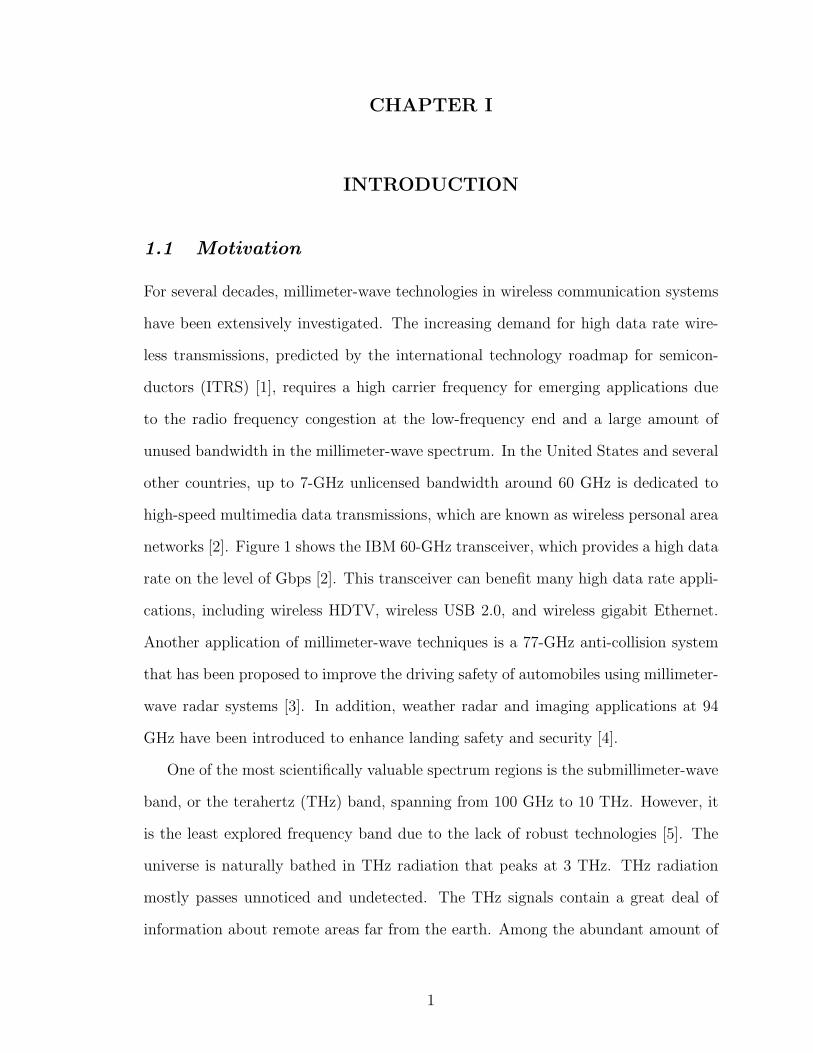
3 The membrane supported planar passive [8]. . . . . . . . . . . . . . . 5
4 The elevated planar passive [11]. . . . . . . . . . . . . . . . . . . . . . 6
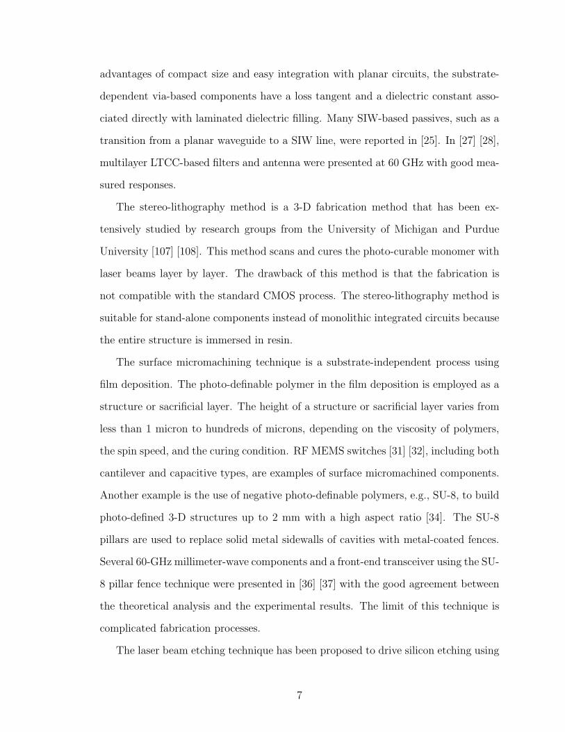
5 The SEM photo of a 2-THz waveguide structure using the laser chem-ical etching technique [111]. . . . . . . . . . . . . . . . . . . . . . . . 8
6 The SEM photo of a waveguide structure using the deep reactive ionetching technique at the Georgia Institute of Technology. . . . . . . . 10
7 The deep reactive ion etching technique: (a) a thin polymer layer fromC4F8 plasma is deposited on all surfaces; (b) the polymer layer is etchedfaster from the base than that from the sidewalls; (c) the exposedsilicon is etched by fluorine species [41]. . . . . . . . . . . . . . . . . . 11
8 The deep reactive ion etching trend [41]. The U denotes the uniformity;the E denotes the etching cycle; P denotes the passivation cycle. Thisfigure gives the e!ect on uniformity, etch rate, selectivity to mask,profile, scalloping, and mask undercut while tuning the SF6 flow, C4F8flow, SF6 time, C4F8 time, pressure, platen power, and coil power. . . 11
9 Fabrication flow of using the deep reactive ion etching technique. Awaveguide passive is made with the use of split-block method by cuttingalong the E-plane center or H-plane center. Each half is fabricatedusing this fabrication flow. Then the fabricated two halves are puttogether to form the waveguide passive. . . . . . . . . . . . . . . . . 13
10 The physical layout of the meander waveguide. It consists of two tran-sition sections and one meander section. . . . . . . . . . . . . . . . . 17
11 The meander section in detail. . . . . . . . . . . . . . . . . . . . . . . 17
12 The optimization response of the meander section. . . . . . . . . . . . 18
13 Tolerances in the fabrication using a H-plane split. . . . . . . . . . . 19
14 SEM photos of two physical characteristics important for practicalwaveguides. . . . . . . . . . . . . . . . . . . . . . . . . . . . . . . . . 19
15 The simulation of re-entrant angle along a H-plane split. . . . . . . . 21
16 Silicon samples and assembled fixture. . . . . . . . . . . . . . . . . . 22
x

17 The measurement setup. . . . . . . . . . . . . . . . . . . . . . . . . . 23
18 The measurement and simulation of the straight waveguide. . . . . . 24
19 The measured and simulated S21 of the straight waveguide. . . . . . . 24
20 The measurement and simulation of the meander waveguide. . . . . . 25
21 The measured and simulated S21 of the meander waveguide. . . . . . 25
22 A comparison of this work with existing works, including microma-chined finite-ground-coplanar (FGC) lines and micromachined rect-coax waveguides. . . . . . . . . . . . . . . . . . . . . . . . . . . . . . 26
23 The physical layout of the waveguide filter. . . . . . . . . . . . . . . . 27
24 The simulated response of the three-pole filter. . . . . . . . . . . . . . 28
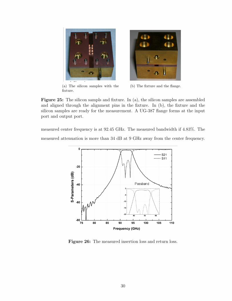
25 The silicon sampls and fixture. In (a), the silicon samples are assembledand aligned through the alignment pins in the fixture. In (b), thefixture and the silicon samples are ready for the measurement. A UG-387 flange forms at the input port and output port. . . . . . . . . . 30
26 The measured insertion loss and return loss. . . . . . . . . . . . . . . 30
27 The simulations of the W -band filter by sweeping the shift of siliconsamples toward the edges from 0-60 µm with a step of 10 µm. Theshift results in a wider opening between adjacent resonators and alarger volume of each resonator. . . . . . . . . . . . . . . . . . . . . . 32
28 Comparison of this work with other existing micromachined filters. . 32
29 The topology of (a) the hybrid coupler and (b) the power divider. . . 34
30 Simulated return loss vs. frequency with di!erent d as well as thephase deviations of ridged waveguide 90 ! phase shifter and a quarterwaveguide phase shifter. . . . . . . . . . . . . . . . . . . . . . . . . . 35
31 Simulated return loss against frequency with di!erent iris thickness. . 36
32 (a) Silicon blocks of the coupler; (b) WR-10 waveguide flange. . . . . 36
33 The S-parameters of the hybrid coupler. . . . . . . . . . . . . . . . . 37
34 The S-parameters of the power divider. . . . . . . . . . . . . . . . . . 38
35 The measured combining e"ciency after cascading the power dividerand hybrid structure. . . . . . . . . . . . . . . . . . . . . . . . . . . . 39
36 An existing wideband CPW-to-waveguide transition [58]. . . . . . . . 41
37 The schematic diagram of the transition. . . . . . . . . . . . . . . . . 43
xi

38 The CPW and the coupling probe (The transition is cut in half alongthe center of the broad wall due to its symmetry, and the metalizedsilicon sidewalls with thickness of T are not shown). . . . . . . . . . . 43
39 The study of parameters: probe height and aperture. . . . . . . . . . 46
40 The study of parameters: CPW tuning stub and coaxial section. . . . 47
41 The simulated insertion loss and return loss of the transition. . . . . . 48
42 The equivalent of this transition. . . . . . . . . . . . . . . . . . . . . 48
43 The back-to-back transition. . . . . . . . . . . . . . . . . . . . . . . . 49
44 The fixture and the device under test. . . . . . . . . . . . . . . . . . . 49
45 The fabrication process flow. In (a), the process flow of using the deepreactive ion etching technique is given. In (b), the process of makingSU-8 pillar and CPW lines on quartz is provided. . . . . . . . . . . . 50
46 SEM photos of the probe and the silicon sample. . . . . . . . . . . . . 51
47 The measured insertion loss and return loss. . . . . . . . . . . . . . . 52
48 The measured and simulated S21 in detail. . . . . . . . . . . . . . . . 52
49 The proposed filter topology. . . . . . . . . . . . . . . . . . . . . . . . 54
50 Transition and filter layer. . . . . . . . . . . . . . . . . . . . . . . . . 55
51 The dimensions of the cavity. . . . . . . . . . . . . . . . . . . . . . . 56
52 The E-field plot of the resonator. . . . . . . . . . . . . . . . . . . . . 57
53 Resonant frequency with varying H and L. . . . . . . . . . . . . . . . 58
54 Resonant frequency vs. W and K vs. gap. . . . . . . . . . . . . . . . 58
55 (a) The probe and CPW. (b) Silicon layer in detail. . . . . . . . . . . 59
56 (a) Four silicon layers to form RWG and filter. (b) Two stacked siliconlayers on fixture. . . . . . . . . . . . . . . . . . . . . . . . . . . . . . 60
57 Simulation and measurement results of band-pass filter with transitions. 61
58 Simulated filter with transitions response versus frequency when thesecond silicon layer undergoes displacement. . . . . . . . . . . . . . . 63
59 The detail in the passband of simulated filter with transitions responseversus frequency when the second silicon layer undergoes displacement. 64
60 Existing tunable cavity filter [82]. . . . . . . . . . . . . . . . . . . . . 66
61 The proposed tunable cavity resonator. . . . . . . . . . . . . . . . . . 68
xii

62 The E-field of the cavity resonator. . . . . . . . . . . . . . . . . . . . 69
63 The dimensions of the cavity. . . . . . . . . . . . . . . . . . . . . . . 70
64 The implementation of the cavity. . . . . . . . . . . . . . . . . . . . . 71
65 Quartz wafer with two dies, the right one assembled with silicon sample. 71
66 SEM picture of the silicon sample. . . . . . . . . . . . . . . . . . . . . 73
67 Simulation of the cavity resonator. . . . . . . . . . . . . . . . . . . . 74
68 Measurement of the cavity resonator. . . . . . . . . . . . . . . . . . . 74
69 Block diagram of a 2-anode 900 GHz balanced tripler. The tripler usesa split-block waveguide design. The diodes are connected in series atdc and are in a balanced configuration at RF. The chip is inserted ina channel between the input and the output rectangular waveguides.An E-plane probe located in the input waveguide couples the signalsat the fundamental frequency to a suspended microstrip line that canpropagate only in a quasi-TEM mode. This line has several sections oflow and high impedances used to match the diodes at the input andoutput frequency and to prevent the third harmonics from leaking intothe input waveguide. The third harmonic produced by the diodes iscoupled to the output waveguide by the second E-plane probe. Ad-ditional waveguide sections of di!erent impedances and lengths (notshown) are used for the input and output matching. !Ef1 and !E3f1
stand respectively for the electric field at the fundamental frequencyf1 and at the output frequency 3!f1. The electric fields and the cur-rent lines are represented for the fundamental frequency f1 (thick lightlines), the idler frequency 2!f1 (dashed lines) and the output frequency3!f1 (light plain lines) . . . . . . . . . . . . . . . . . . . . . . . . . . 81
70 The anti-parallel configuration of diodes. . . . . . . . . . . . . . . . . 82
71 The drawing of half of the entire 900 GHz frequency tripler. Thewaveguide structure is cut along the E-plane center. . . . . . . . . . . 83
72 The design methodology of the frequency tripler [125]. . . . . . . . . 85
73 The three-dimension model of the Schottky diode. . . . . . . . . . . . 86
74 The depiction of the micromachining process used to form the horn:(a) half of the horn split along the E-plane center; (b) silicon part ontop of the fixture; (c) silicon part only. . . . . . . . . . . . . . . . . . 88
75 The simulated far-field patterns of the 900 GHz micromachined horn. 89
76 The fixture and the silicon circuits for measurement. A UG-387 waveg-uide flange forms at the input waveguide. . . . . . . . . . . . . . . . . 90
xiii

77 The tripler chip in the micromachined waveguide structures. The metalbeam leads on the THz chip greatly improve the chip handling andmake the assembly highly repeatable. . . . . . . . . . . . . . . . . . . 91
78 The measurement setup. From the left to the right, the measurementchain consists of a W -band power amplifier, a rotary vane attenuator,a W-band coupler, an isolator, a WR10 waveguide, a JPL in-house300-GHz tripler, the 900-GHz tripler, a circular to WR10 transition, aWR-10 waveguide, and a PM2 power meter. . . . . . . . . . . . . . . 92
79 The estimate and measured output power and e"ciency at room tem-perature. No corrections have been made to the measured outputpower and e"ciency numbers. At room temperature, the measuredoutput power was 23.7 µW to 85.3 µW from 828 GHz to 963 GHz. . 93
80 SEM images: (a) output horn; (b) input waveguide; (c) cross sectionof waveguide sidewall; (d) surface roughness on sidewall; (e) the inputand output backshorts as well as the chip channel. . . . . . . . . . . . 95
81 The measured output power and measured e"ciency v.s. input powerat 909 GHz. . . . . . . . . . . . . . . . . . . . . . . . . . . . . . . . . 96
xiv

SUMMARY
This research discusses the design, fabrication, integration, and characterization
of micromachined millimeter-wave components and a signal source for submillimeter-
wave multiplier source using the deep reactive ion etching technique. A wide range
of micromachined millimeter-wave components are presented in this thesis. Micro-
machined low-loss straight and meander waveguides from 75 GHz to 110 GHz are
reported first. The tolerances of a micromachined straight waveguide are analyzed.
Next, a micromachined W -band bandpass filter is introduced. The three-pole
Chebysche! bandpass filter has 0.5-dB ripples in the passband and at least 30-dB
attenuation at 9 GHz away from the center frequency. The passband insertion loss is
only 1.1 dB to 1.3 dB with a bandwidth of 4.83%. Then, a W -band hybrid coupler and
a W -band power divider are presented. The hybrid coupler and the power divider are
designed in the H-plane of a rectangular waveguide. The hybrid coupler uses a ridged
waveguide 90! phase shifter to reduce phase deviation and a joint waveguide to achieve
a broad bandwidth. The power divider employs a T -shape topology. The measured
response presented in this work shows good agreement with simulated response. The
power divider and the hybrid coupler cascade, and a measured combining e"ciency
is reported.
The next two chapters demonstrate a novel micromachined wideband transition
from a coplanar waveguide (CPW) to a rectangular waveguide (RWG) from 75 GHz
to 110 GHz and a waveguide filter taking full advantage of this transition. The
comprehensive analysis of the transition and the study on parameters are given in
detail. In the proposed filter design, metal-coated probes are used to couple signals
xv

from CPW lines to cavity-based resonators. The waveguide-based input and output
ports are no longer needed. This design significantly reduces the size of the filter. The
measured response has a center frequency of 96.6 GHz, a bandwidth of 2.9%, and a
passband insertion loss of 4.14 dB. Chapter 7 introduces a high quality factor (high-Q)
tunable cavity resonator. This proposed design tackles the problem of using planar
element to tune the resonance of a 3-D cavity resonator. Therefore, reconfigurable
cavity-based components are enabled by the proposed tunable resonator for wireless
communication systems.
The second topic of this thesis investigates the signal generation at submillimeter-
wave frequency range. A wideband 900 GHz frequency multiplier is designed, imple-
mented, and integrated in a micromachined waveguide structure. The input signals
are generated by a 300 GHz tripler and coupled to a suspend microstrip line that
supports the propagation in a TEM mode through an E-plane probe. The generated
third harmonic signals are coupled to an output waveguide through the output E-
plane probe. The design, simulation, fabrication, and measurement of the 900 GHz
frequency multiplier are presented in detail.
xvi
CHAPTER I
INTRODUCTION
1.1 Motivation
For several decades, millimeter-wave technologies in wireless communication systems
have been extensively investigated. The increasing demand for high data rate wire-
less transmissions, predicted by the international technology roadmap for semicon-
ductors (ITRS) [1], requires a high carrier frequency for emerging applications due
to the radio frequency congestion at the low-frequency end and a large amount of
unused bandwidth in the millimeter-wave spectrum. In the United States and several
other countries, up to 7-GHz unlicensed bandwidth around 60 GHz is dedicated to
high-speed multimedia data transmissions, which are known as wireless personal area
networks [2]. Figure 1 shows the IBM 60-GHz transceiver, which provides a high data
rate on the level of Gbps [2]. This transceiver can benefit many high data rate appli-
cations, including wireless HDTV, wireless USB 2.0, and wireless gigabit Ethernet.
Another application of millimeter-wave techniques is a 77-GHz anti-collision system
that has been proposed to improve the driving safety of automobiles using millimeter-
wave radar systems [3]. In addition, weather radar and imaging applications at 94
GHz have been introduced to enhance landing safety and security [4].
One of the most scientifically valuable spectrum regions is the submillimeter-wave
band, or the terahertz (THz) band, spanning from 100 GHz to 10 THz. However, it
is the least explored frequency band due to the lack of robust technologies [5]. The
universe is naturally bathed in THz radiation that peaks at 3 THz. THz radiation
mostly passes unnoticed and undetected. The THz signals contain a great deal of
information about remote areas far from the earth. Among the abundant amount of
1

information, the dynamic properties of a wide range of molecules in remote regions
are hidden. The structures of molecules can be studied through the observation
of molecule resonances. Furthermore, the unique properties of THz signals enable
many applications in radio astronomy, plasma fusion diagnostics, atmospheric earth
observation, molecular spectroscopy, and high-resolution imaging. In the application
of atmospheric earth observation, the investigation of the correlation between the
shape of the ozone hole and the distribution of chlorine monoxide tackles the puzzle
of how human activities a!ect the health of our planet. Figure 2 presents an image
taken by the submillimeter-wave instrument on a NASA satellite of the ozone hole
over Antarctica in 2004 [6].
Figure 1: The IBM 60 GHz transceiver [2].
1.2 Background
Until the early 1980’s, most of the millimeter-wave components were fabricated using
waveguide passives. Waveguide passives are low loss, high power capacity, and high
quality factor, but they are bulky and heavy for applications that have stringent size
and weight requirements. Furthermore, the conventional machining cost of waveguide
2

Figure 2: The ozone hole on 4 October 2004 as mea-sured by the ozone monitoring instrument on the Aurasatellite. Values are in Dobson units. The edge of thehole is defined by the 220 Dobson unit contour [6].
passives is becoming extremely prohibitive when the operating frequency is in the THz
band and the wavelength is in the submillimeter range. Di!erent from the conven-
tional machining technique, micromachining techniques, including photolithography,
etching, and film deposition, originally developed in the semiconductor industry, were
pioneered by research groups at the University of Michigan and Caltech two decades
ago to achieve good performance in the millimeter-wave frequency range [7]. Micro-
machining techniques are capable of improving the performance and lowering the cost
of millimeter-wave and submillimeter-wave components.
Two types of micromachined passives, planar passives and three-dimension (3-D)
passives, have been extensively studied in the literature [8]. Planar passives, using
3

either a microstrip or a coplanar waveguide, have been widely used in millimeter-wave
circuits. The performance of planar passives inevitably deteriorates with increased
operating frequencies because of frequency dispersion, substrate dependence, and
dielectric loss that is approximately propotional to operating frequencies. Microma-
chined planar passives with reduced dielectric loss have been enabled by the following
approaches:
• Having membrane-supported components with reduced e!ective dielectric con-
stants by partially removing a substrate [9] [10], shown in Figure 3.
• Elevating planar circuits in the air [11].
• Adding a low-loss, low dielectric constant (low-k) layer between circuits and
high dielectric constant substrates [12] [13].
• Reducing the dielectric constant of a substrate using chemical reactions [14].
Micromachined planar circuits with reduced conductor loss are enabled by either
an electroplating technique [15] [16] or a high-temperature superconductor (HTS)
[17] [18]. The electroplating technique that changes the geometry of planar transmis-
sion lines is e!ective at reducing conductor loss, especially when the skin depth at
operating frequencies is close to the thickness of the transmission lines. HTS, discov-
ered in 1911 with hundreds of variations, has a fabrication process that is compatible
with monolithic microwave circuits. The most widely-used HTS films are the yttrium
barium copper oxide (YBCO) film and the thallium barium calcium copper oxide
(TBCCO) film [19] [20].
With the micromachined techniques discussed above, many planar millimeter-
wave components have been reported with enhanced performance. In [21], a patch
antenna on a membrane-supported substrate was characterized. The bandwidth of
the antenna was increased by 64%, and the e"ciency was increased by as much as
4
Figure 3: The membrane supported planar passive [8].
28%. In [22], a W -band five-section bandpass filter showed a passband insertion loss
of 3.6 dB with a bandwidth of 6.1%. The circuits of the filter were fabricated on top
of a dielectric membrane and assembled in a shielded membrane microstrip structure.
In [23], an elevated CPW line was fabricated by removing the silicon between the
signal line and the ground planes. The attenuation was improved by more than 20%.
In [11], a coupler was introduced to cover the frequency range from 15 GHz to 45
GHz, shown in Figure 4. The frequency dispersion of the coulper were significantly
reduced by elevating the lines in the air. In [24], the low dielectric constant and
low-loss materials were applied on top of a silicon substrate to reduce the e!ective
dielectric constant of planar transmission lines. A 10-µm thick polymer layer was
used to reduce the e!ective dielectric constant. Thus, a 50% reduction of insertion
loss was achieved with the increased quality factor by 30%"50%. In [14], a 50-µm
deep trench was etched on silicon and filled with silicon dioxide using a low-pressure
chemical vapor deposition process, and finite ground coplanar waveguide lines were
fabricated on top of the trenches. Measured results of the waveguide lines showed
an attenuation of 1.5 dB/cm at 20 GHz. The low attenuation came from increased
5

substrate resistivity and decreased e!ective dielectric constant.
Figure 4: The elevated planar passive [11].
Micromachined 3-D passives have attracted considerable attention recently due to
their intrinsic superior quality factors over planar passives. Advanced micromachining
techniques have made these 3-D circuits feasible in the millimeter and submillimeter-
wave frequency ranges. Micromachined 3-D circuits with high precision are critical
for the delivery of a!ordable and high-performance submillimeter-wave components.
Micromachining techniques for 3-D components include the following approaches:
• The via-based multilayer technique
• The sterero-lithography technique
• The surface micromachining technique
• The laser-based etching technique
• The bulk micromachining technique
The via-based multilayer technique has been widely used in substrate integrated
waveguides (SIW) [25] [26] and multilayer LTCC components [27] [28]. Despite its
6
advantages of compact size and easy integration with planar circuits, the substrate-
dependent via-based components have a loss tangent and a dielectric constant asso-
ciated directly with laminated dielectric filling. Many SIW-based passives, such as a
transition from a planar waveguide to a SIW line, were reported in [25]. In [27] [28],
multilayer LTCC-based filters and antenna were presented at 60 GHz with good mea-
sured responses.
The stereo-lithography method is a 3-D fabrication method that has been ex-
tensively studied by research groups from the University of Michigan and Purdue
University [107] [108]. This method scans and cures the photo-curable monomer with
laser beams layer by layer. The drawback of this method is that the fabrication is
not compatible with the standard CMOS process. The stereo-lithography method is
suitable for stand-alone components instead of monolithic integrated circuits because
the entire structure is immersed in resin.
The surface micromachining technique is a substrate-independent process using
film deposition. The photo-definable polymer in the film deposition is employed as a
structure or sacrificial layer. The height of a structure or sacrificial layer varies from
less than 1 micron to hundreds of microns, depending on the viscosity of polymers,
the spin speed, and the curing condition. RF MEMS switches [31] [32], including both
cantilever and capacitive types, are examples of surface micromachined components.
Another example is the use of negative photo-definable polymers, e.g., SU-8, to build
photo-defined 3-D structures up to 2 mm with a high aspect ratio [34]. The SU-8
pillars are used to replace solid metal sidewalls of cavities with metal-coated fences.
Several 60-GHz millimeter-wave components and a front-end transceiver using the SU-
8 pillar fence technique were presented in [36] [37] with the good agreement between
the theoretical analysis and the experimental results. The limit of this technique is
complicated fabrication processes.
The laser beam etching technique has been proposed to drive silicon etching using
7
chemical reactions. A laser-assisted chemical etching system is summarized in [38].
The Cl2 gas is used to accelerate the etching process. The laser beam etching can
achieve complicated 3-D structures in a small area. In [111], a laser-etched feedhorn
structure on silicon was presented. The laser beam etching technique is very useful
for THz components operating above 500 GHz. Figure 5 shows a 2-THz waveguide
structure fabricated using the laser beam chemical etching technique at the University
of Arizona.
Figure 5: The SEM photo of a 2-THz waveguide struc-ture using the laser chemical etching technique [111].
Two bulk silicon micromachining techniques, wet etching and dry etching, have
been extensively investigated and reported in [38] [111]. For wet etching, many chem-
icals are commercially available. The selection of an etchant depends on the type of
etching, the properties of a material, the material of masks, and its compatibility with
existing circuits. Two types of wet etching are isotropic wet etching and anisotropic
wet etching. In isotropic wet etching, etching speeds are almost the same in all di-
rections. One type of isotropic etchant is HNA, which consists of hydrofluoric acid,
8
nitric acid, and acetic acid. A layer of silicon dioxide or silicon nitride is typically
used as the mask layer of this type of etchant. Di!erent from isotropic silicon etch-
ing, anisotropic silicon etching is commonly used in micromachining techniques. In
anisotropic silicon etching, the etching speed depends on the crystallographic direc-
tion. For this reason, it is called orientation-dependent etching. The etching rate on
the <111> plane of silicon wafers is remarkably slower than that on the other planes.
Eventually, the <111> plane that has the slowest etching rate is exposed. When two
wet-etched silicon samples bond, a waveguide structure [38] can form. One of the
widely used chemicals for anisotropic etching is KOH, a hydroxide of alkali metal.
KOH etching can result in a very smooth and shining finish, which distinguishes it
from other etchants such as tetramethyl ammonium hydroxide (TMAH).
Dry etching was invented in the 1970’s to solve the lack of a satisfactory silicon
nitride etchant, particularly when aluminum lines were exposed [50]. Powered by
external radio frequency energy, dry etching can be operated below 350 !C, even at
room temperature in a plasma environment. One dry etching technique, the deep
reactive ion etching technique, powered by inductively coupled high-density plasma,
is capable of achieving a high aspect ratio up to 20:1 with a nearly 90 ! sidewall. This
deep reactive ion etching process consists of a passivation cycle and an etching cycle.
The use of the deep reactive ion etching technique has been reported in millimeter-
wave components, e.g., a microstrip to rectangular waveguide transition [116]. Figure
6 depicts a micromachined waveguide structure using the deep reactive ion etching
technique.
1.3 Enabling Technology: The Deep Reactive Ion EtchingTechnique
The mechanism of the deep reactive ion etching process is introduced in this section
to provide a general guideline for the fabrication of the proposed passives in the
following chapters. Figure 7 illustrates this process [41]. The deep reactive ion etching
9
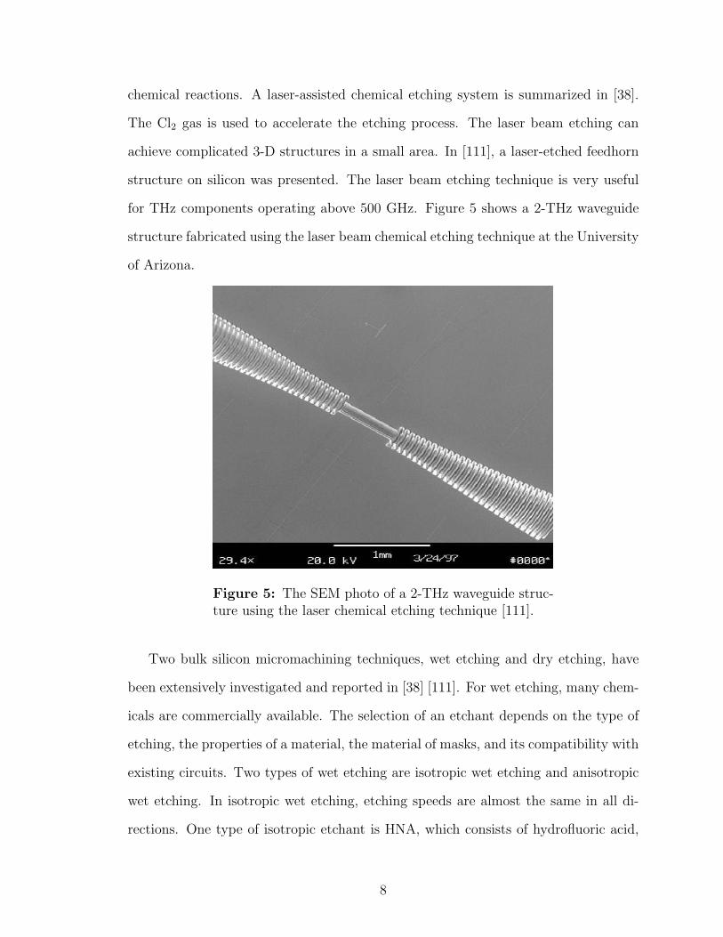
Figure 6: The SEM photo of a waveguide structure us-ing the deep reactive ion etching technique at the GeorgiaInstitute of Technology.
technique is a dry etching process that consists of two cycles: a passivation cycle
and an etching cycle. In the passivation cycle, the plasma of C4F8 deposits a thin
polymer layer on all surfaces. In the etching cycle, the gases of SF6 and Ar are used.
Accelerated by external radio frequency energy, the ion bombardment removes the
polymer layer on the base much faster than that on the sidewalls. Once the silicon
is exposed, the wafer is etched by fluorine species from the plasma of SF6. The two
cycles are alternatively repeated until a desired depth is reached.
In the following projects presented in this thesis, a straight sidewall close to 90 !
is expected. In reality, however, the profile of trenches is a!ected by many factors,
including the pressure in an etching chamber, the flow rate of gases, the time for
etching and passivation, the power of etching and passivation, and the exposed area
of the silicon. Tuning these parameters in an inductively coupled plasma etcher to
find a perfect recipe is a trial-and-error and time-consuming process. Therefore, un-
derstanding which knob to tune is crucial to achieving a nearly 90 ! sidewall. Figure 8
depicts the e!ects on sidewalls while the parameters of flow rates, time, pressure, and
10

power are being tuned [41].
Figure 7: The deep reactive ion etching technique: (a) a thin polymer layer fromC4F8 plasma is deposited on all surfaces; (b) the polymer layer is etched faster fromthe base than that from the sidewalls; (c) the exposed silicon is etched by fluorinespecies [41].
Figure 8: The deep reactive ion etching trend [41]. The U denotes theuniformity; the E denotes the etching cycle; P denotes the passivationcycle. This figure gives the e!ect on uniformity, etch rate, selectivityto mask, profile, scalloping, and mask undercut while tuning the SF6flow, C4F8 flow, SF6 time, C4F8 time, pressure, platen power, and coilpower.
1.4 Process Flow
Figure 9 shows the process flow to fabricate millimeter and submillimeter-wave com-
ponents using the deep reactive ion etching technique. First, a silicon wafer is rinsed
to remove the organic residues. Then, a layer of silicon dioxide is deposited on both
11

sides of the wafer using the plasma-enhanced chemical vapor deposition process. Af-
ter the deposition, a layer of photoresist is spun and patterned on top of the silicon
dioxide layer. The exposed silicon dioxide layer is etched away using the dry-etching
technique. After the photoresist residues are removed, the patterned silicon wafer is
etched using the deep reactive ion etching technique for the desired depth. Then, the
silicon wafer is flipped over, and the process is repeated starting from the spinning
of the photoresist. Finally, the micromachined samples are released after removing
the silicon dioxide layer. A thick metal layer of Ti/Cu/Au is deposited to form the
metalized surfaces of waveguide structures. According to Equation 1, the skin depth
is inversely proportional to the square root of operating frequencies. At 60 GHz, the
skin depth of copper is about 0.2 µm. Therefore, a 1-µm thick metal layer behaves
electrically as well as a solid conduct wall. The skin depth, "s, is given in the following
equation:
"s =
!2
#µ0µr$(1)
where $ is the bulk conductivity in Simen/meter, µ0 is the permeability constant
= 4% # 10"7 Henry/meter, and µr is the relative permeability.
1.5 Advantages of the Deep Reactive Ion Etching Method
In this research, a wide range of millimeter and submillimeter-wave components have
been designed, fabricated, and characterized. Compared to other 3-D micromachin-
ing techniques, the deep reactive ion etching technique is suitable for mass production
because it is a low-cost, parallel process. The process flow is CMOS compatible re-
gardless of the crystal orientation of silicon wafers. In particular, the mechanical
and chemical properties of silicon wafers have been extensively studied. In addi-
tion, no dielectric filling eliminates dielectric loss, which is the dominant loss at the
high-frequency end. Therefore, the deep reactive ion etching technique is feasible
12
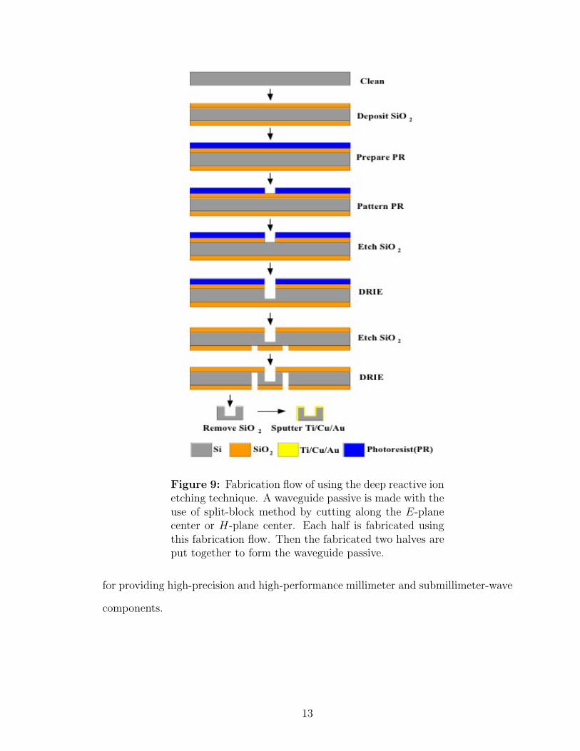
Figure 9: Fabrication flow of using the deep reactive ionetching technique. A waveguide passive is made with theuse of split-block method by cutting along the E-planecenter or H-plane center. Each half is fabricated usingthis fabrication flow. Then the fabricated two halves areput together to form the waveguide passive.
for providing high-precision and high-performance millimeter and submillimeter-wave
components.
13
1.6 Contribution and Organization
In this work, the electrical performance of millimeter and submillimeter-wave com-
ponents is investigated in the frequency band spanning from 60 GHz to 900 GHz.
Chapter 2 investigates micromachined straight and meander waveguides from 75 GHz
to 110 GHz using the deep reactive ion etching technique and analyze the tolerances
of a micromachined straight waveguide. The results show that the straight waveguide
has a measured insertion loss of 0.23 dB/cm"0.42 dB/cm from 85 GHz to 105 GHz.
The meander waveguide has the measured insertion loss of 0.41 dB/cm"0.69 dB/cm
from 90 GHz to 110 GHz.
Then, chapter 3 introduces a micromachined W -band bandpass filter. The three-
pole Chebysche! bandpass filter has 0.5-dB ripples in the passband and at least 30 dB
attenuation at 9 GHz away from the center frequency. The measured center frequency
is at 92.45 GHz. The passband insertion loss is between 1.1 dB and 1.3 dB with a
bandwidth of 4.83 %. The measured responses demonstrate the feasibility of using
the silicon micromachining technique to fabricate low-loss millimeter-wave passives.
Chapter 4 presents a W -band hybrid coupler and a W -band power divider. In this
project, the hybrid coupler and the power divider are designed in the H-plane of a
rectangular waveguide. The hybrid coupler uses a ridged waveguide 90 ! phase shifter
to reduce phase deviation and a joint waveguide to achieve a broad bandwidth. The
power divider utilizes a T -shaped topology. The simulated and measured responses
show good agreement. Measured combining e"ciency is reported by cascading the
power divider and hybrid coupler.
Chapter 5 shows a novel micromachined wideband transition from a coplanar
waveguide (CPW) to a rectangular waveguide from 75 GHz to 110 GHz. The transi-
tion is suitable for integration with planar circuits. The measured insertion loss of a
back-to-back structure is 2.25 dB, and the measured return loss is better than 11 dB
over the entire W -band. This transition is comprehensively analyzed and reported.
14

Chapter 6 introduces a waveguide filter that takes full advantage of the above
transition. In the proposed filter, metal-coated probes are used to couple signals
from CPW lines to cavity-based resonators. Therefore, the waveguide-based input
and output ports are no longer needed. This design significantly reduces the size
of the proposed filter. A measured response has a center frequency of 96.6 GHz, a
bandwidth of 2.9%, and a passband insertion loss of 4.14 dB.
Chapter 7 presents high-Q tunable cavity resonators using planar tuning com-
ponents. This project tackles the problem of using planar components to tune the
resonance of a 3-D cavity resonator. This tunable cavity resonator can be used in the
design of reconfigurable cavity-based modules for wireless communication systems.
Chapter 8 presents a 900-GHz frequency tripler with micromachined waveguide
structures. The input of this 900-GHz tripler, powered by a 300-GHz tripler, is
pumped into an input waveguide. The signals are coupled to a suspended microstrip
line that supports the propagation in a TEM mode using an E-plane probe. The high
and low impedance sections in the microstrip line assist the impedance matching
of diodes and isolate the third harmonic signals from the input waveguide. The
generated third harmonic signals are coupled to an output waveguide through the
second E-plane probe. The background of THz signal sources, the design methodology
of frequency multipliers, the topology of balanced diodes, the optimization of the use
of full-wave simulators, and the measurement of the 900-GHz tripler are presented
in detail. Finally, chapter 9 concludes the thesis by listing the contributions of the
research and the publications of this work to date.
15
CHAPTER II
A W -BAND STRAIGHT WAVEGUIDE AND A W -BAND
MEANDER WAVEGUIDE
In this chapter, a W -band straight waveguide and a W -band meander waveguide are
designed and characterized to define the electrical performance of silicon microma-
chined waveguides using the deep reactive ion etching technique [42]. The microma-
chined W -band straight waveguide is a fundamental block to build more complicate
waveguide passives. The meander waveguide can be used in traveling wave tubes
that provide amplified radio frequency signals using an external electron beam. A
high-frequency traveling wave tube is benefited from the demonstration of this mi-
cromachined W -band meander waveguide.
2.1 Meander Waveguide
Figure 10 shows the physical layout of the meander waveguide, which is designed
in the E-plane of a waveguide. The meander waveguide consists of three sections:
transition, meander, and transition. The meander section is optimized to achieve
the minimum insertion loss. Two transitions connect the W -band signals from input
and output to the meander section. Figure 11 shows the meander section in detail.
The meander section has a height of 2.54 mm. The input and output use standard
WR-10 waveguide flange. In Figure 11 , B denotes the width of the meander section.
L denotes the length of the straight waveguide between two turns, and P denotes the
diameter of an E-plane bend that connects the two straight parts. P is selected to
be 0.427&g for a compact size. After the full-wave simulation using Ansofts HFSS, L
equals to 0.831&g, and B equals to 0.118&g , where &g is the guided wavelength at
16

the center frequency. &g is given in Equation 2 for a TE10 mode.
Figure 10: The physical layout of the meander waveg-uide. It consists of two transition sections and one me-ander section.
Figure 11: The meander section in detail.
&g =&"
1" ( !2a)2
(2)
where a is the width of a rectangular waveguide and & is the free space wavelength
at the center frequency.
To optimize the transitions, a linear taper is chosen for its low insertion loss
and easy fabrication. The electrical performance of the whole meander waveguide is
simulated and reported in Figure 12. The dimensions are summarized in Table 1.
17

Figure 12: The optimization response of the meandersection.
Table 1: Dimensions of the meander waveguide.
Dimensions Value (mm)P 1.8L 3.5B 0.5
Length of the transition 7.2
2.2 Straight Waveguide
A 1-inch long WR-10 straight waveguide is fabricated using the deep reactive ion
etching technique. Figure 13 depicts a waveguide structure, which is cut in half
along the center of the H-plane of a waveguide. Each half of the waveguide is etched
individually and is assembled together to form the waveguide structure.
The two important tolerances in the deep reactive ion etching process are vertical
striation and re-entrant angle. These two tolerances are drawn exaggeratedly in
Figure 13 to show the details. The SEM photos of tolerances are shown in Figure 14.
The re-entrant sidewall in a silicon trench comes from the lack of polymer if the time
18

Figure 13: Tolerances in the fabrication using a H-plane split.
(a) Re-entrent angle.
(b) Vertical striation.
Figure 14: SEM photos of two physical characteristics important for practical waveg-uides.
19
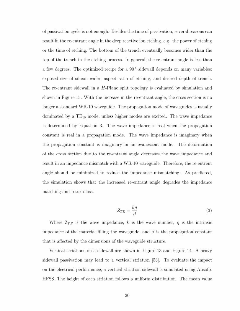
of passivation cycle is not enough. Besides the time of passivation, several reasons can
result in the re-entrant angle in the deep reactive ion etching, e.g. the power of etching
or the time of etching. The bottom of the trench eventually becomes wider than the
top of the trench in the etching process. In general, the re-entrant angle is less than
a few degrees. The optimized recipe for a 90 ! sidewall depends on many variables:
exposed size of silicon wafer, aspect ratio of etching, and desired depth of trench.
The re-entrant sidewall in a H-Plane split topology is evaluated by simulation and
shown in Figure 15. With the increase in the re-entrant angle, the cross section is no
longer a standard WR-10 waveguide. The propagation mode of waveguides is usually
dominated by a TE10 mode, unless higher modes are excited. The wave impedance
is determined by Equation 3. The wave impedance is real when the propagation
constant is real in a propagation mode. The wave impedance is imaginary when
the propagation constant is imaginary in an evanescent mode. The deformation
of the cross section due to the re-entrant angle decreases the wave impedance and
result in an impedance mismatch with a WR-10 waveguide. Therefore, the re-entrent
angle should be minimized to reduce the impedance mismatching. As predicted,
the simulation shows that the increased re-entrant angle degrades the impedance
matching and return loss.
ZTE =k'
((3)
Where ZT E is the wave impedance, k is the wave number, ' is the intrinsic
impedance of the material filling the waveguide, and ( is the propagation constant
that is a!ected by the dimensions of the waveguide structure.
Vertical striations on a sidewall are shown in Figure 13 and Figure 14. A heavy
sidewall passivation may lead to a vertical striation [53]. To evaluate the impact
on the electrical performance, a vertical striation sidewall is simulated using Ansofts
HFSS. The height of each striation follows a uniform distribution. The mean value
20
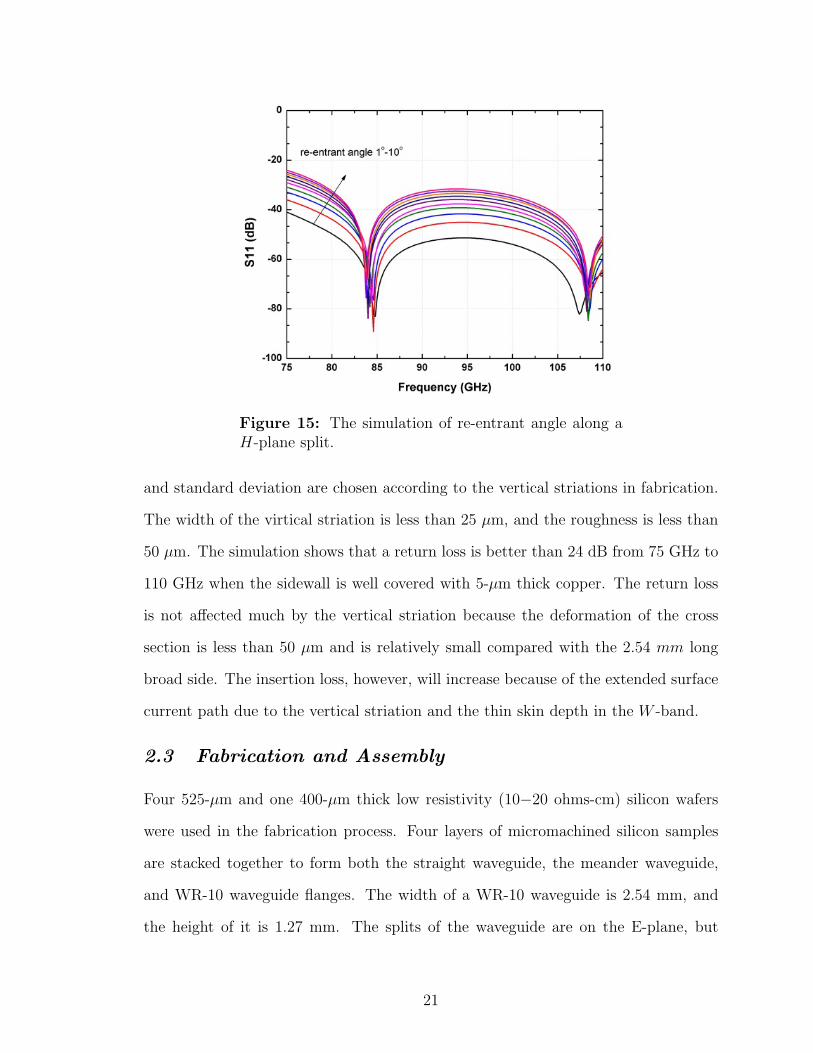
Figure 15: The simulation of re-entrant angle along aH-plane split.
and standard deviation are chosen according to the vertical striations in fabrication.
The width of the virtical striation is less than 25 µm, and the roughness is less than
50 µm. The simulation shows that a return loss is better than 24 dB from 75 GHz to
110 GHz when the sidewall is well covered with 5-µm thick copper. The return loss
is not a!ected much by the vertical striation because the deformation of the cross
section is less than 50 µm and is relatively small compared with the 2.54 mm long
broad side. The insertion loss, however, will increase because of the extended surface
current path due to the vertical striation and the thin skin depth in the W -band.
2.3 Fabrication and Assembly
Four 525-µm and one 400-µm thick low resistivity (10"20 ohms-cm) silicon wafers
were used in the fabrication process. Four layers of micromachined silicon samples
are stacked together to form both the straight waveguide, the meander waveguide,
and WR-10 waveguide flanges. The width of a WR-10 waveguide is 2.54 mm, and
the height of it is 1.27 mm. The splits of the waveguide are on the E-plane, but
21
not along the center. The current path is cut if a small gap exists between two
adjacent samples. This current discontinuity can result in a radiation loss, which will
deteriorate the insertion loss. Alignment pins are used to align the stacked silicon
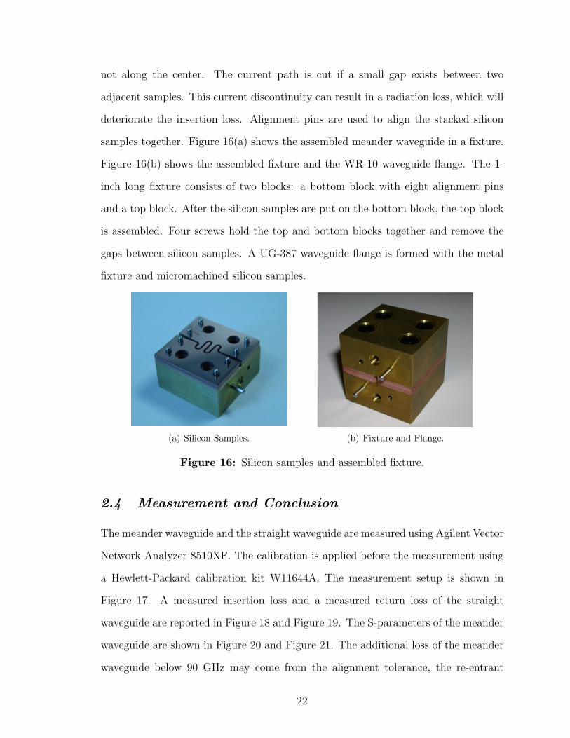
samples together. Figure 16(a) shows the assembled meander waveguide in a fixture.
Figure 16(b) shows the assembled fixture and the WR-10 waveguide flange. The 1-
inch long fixture consists of two blocks: a bottom block with eight alignment pins
and a top block. After the silicon samples are put on the bottom block, the top block
is assembled. Four screws hold the top and bottom blocks together and remove the
gaps between silicon samples. A UG-387 waveguide flange is formed with the metal
fixture and micromachined silicon samples.
(a) Silicon Samples. (b) Fixture and Flange.
Figure 16: Silicon samples and assembled fixture.
2.4 Measurement and Conclusion
The meander waveguide and the straight waveguide are measured using Agilent Vector
Network Analyzer 8510XF. The calibration is applied before the measurement using
a Hewlett-Packard calibration kit W11644A. The measurement setup is shown in
Figure 17. A measured insertion loss and a measured return loss of the straight
waveguide are reported in Figure 18 and Figure 19. The S-parameters of the meander
waveguide are shown in Figure 20 and Figure 21. The additional loss of the meander
waveguide below 90 GHz may come from the alignment tolerance, the re-entrant
22

sidewall, and the undercut in the fabrication. The measured insertion loss of the
straight waveguide is between 0.23-0.42 dB/cm over 85 GHz-105 GHz. The insertion
loss of the meander waveguide is between 0.41-0.69 dB/cm over 90 GHz-110 GHz.
The measured results show great response compared with the existing waveguides
published in the literature. In [43], the attenuation of a planar CPW line is about 1.5
dB/mm on a normal silicon wafer and about 0.5 dB/mm on a grooved silicon wafer.
In [45], the microstrip line is characterized up to 90 GHz. The measured result has
an insertion loss of 0.15 dB/mm at 90 GHz. The metal WR-10 waveguides reported
by Aerowave have the loss of 2-1.4 dB/FT [44].
Figure 17: The measurement setup.
Figure 22 gives the comparison of this work with the existing W -band 3-D mi-
cromachined waveguides and planar waveguides that are on low-loss substrates, e.g.
liquid crystal polymer, GaAs, and polyimide. The comparison shows the microma-
chined waveguides using the deep reactive ion etching technique have the competing
performance compared with other 3-D micromachined waveguides and much less at-
tenuation loss compared to the planar passives.
23

Figure 18: The measurement and simulation of thestraight waveguide.
75 80 85 90 95 100 105 110-10
-5
0
5
10
75 80 85 90 95 100 105 110-10
-5
0
5
10
S-Pa
ram
eter
s (d
B)
Frequency (GHz)
S21_meas S21_sim
Figure 19: The measured and simulated S21 of thestraight waveguide.
24
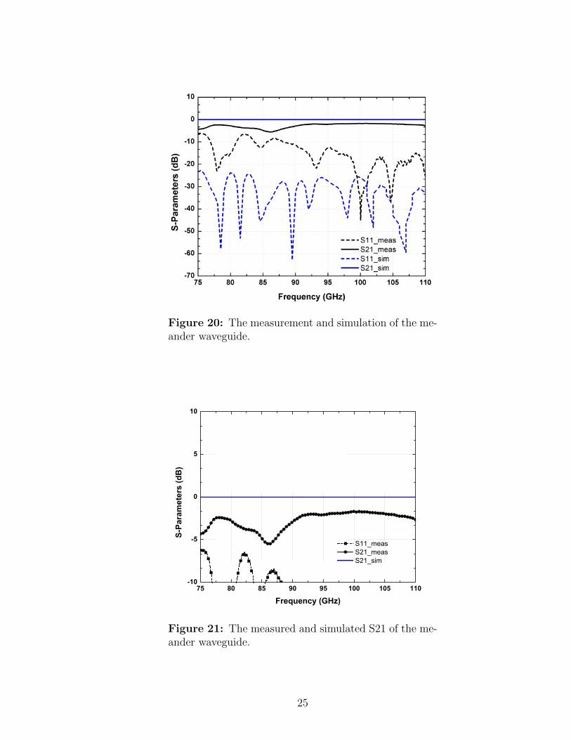
Figure 20: The measurement and simulation of the me-ander waveguide.
75 80 85 90 95 100 105 110-10
-5
0
5
10
S11_meas S21_meas S21_sim
S-Pa
ram
eter
s (d
B)
Frequency (GHz)
Figure 21: The measured and simulated S21 of the me-ander waveguide.
25

Figure 22: A comparison of this work with existing works, includingmicromachined finite-ground-coplanar (FGC) lines and micromachinedrect-coax waveguides.
26
CHAPTER III
A W -BAND THREE-POLE BANDPASS WAVEGUIDE
FILTER
3.1 Design Topology
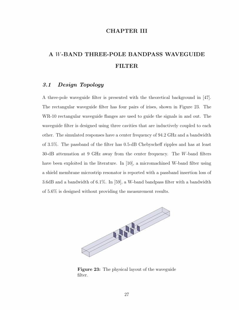
A three-pole waveguide filter is presented with the theoretical background in [47].
The rectangular waveguide filter has four pairs of irises, shown in Figure 23. The
WR-10 rectangular waveguide flanges are used to guide the signals in and out. The
waveguide filter is designed using three cavities that are inductively coupled to each
other. The simulated responses have a center frequency of 94.2 GHz and a bandwidth
of 3.5%. The passband of the filter has 0.5-dB Chebysche! ripples and has at least
30-dB attenuation at 9 GHz away from the center frequency. The W -band filters
have been exploited in the literature. In [10], a micromachined W-band filter using
a shield membrane microstrip resonator is reported with a passband insertion loss of
3.6dB and a bandwidth of 6.1%. In [59], a W-band bandpass filter with a bandwidth
of 5.6% is designed without providing the measurement results.
Figure 23: The physical layout of the waveguidefilter.
27

3.2 Simulation
The guided wavelengths are calculated at the center frequency. The normalized pro-
totype frequencies are determined, and the attenuation is predicted. Then, the di-
mensions of coupling irises and the space between these coupling irises are obtained
using the equations in [48] [49]. Finally, the filter is optimized using a full-wave sim-
ulator, Ansoft’s HFSS 9.2. A copper layer is used to cover all of the internal surfaces
of the waveguide structure. The input and output are inductively coupled to the first
and the third resonators. These two resonators are coupled to the resonator in the
middle respectively. The optimized S-parameters are reported in Figure 24.
Figure 24: The simulated response of the three-polefilter.
3.3 Fabrication and Measurement
Four 525-µm thick silicon layers were used and were denoted as S1, S2, S3, and S4
from top to bottom. The S1 and S4 were etched on top for a depth of 110 µm and were
released from back with a di!erent pattern. The S2 and S3 were etched from both
sides with the same pattern. The first step of the preparation was a wafer cleaning
28

process. Then, a silicon dioxide layer with a thickness of 3.3 µm was deposited on top
of the wafer using Uniaxis PECVD. After the silicon dioxide deposition, photoresist
was spun on top of it. The exposed silicon oxide layer was etched using dry etching.
Finally, the photoresist residue was removed and the silicon was etched using STS
ICP with the deep reactive ion etching process for a depth of 110 µm. The silicon
substrate was flipped after the dry etching and was released from the back. The
metallization was applied on both sides of the silicon samples with Ti and Cu for a
total thickness of 5 µm.
A re-entrant angle is observed in the deep reactive ion etching processing. In our
process, the re-entrant angle is usually less than four degrees. However, for a 525-µm
thick wafer, a 4 degree re-entrant angle equals to a 36.7-µm di!erence when the wafer
is etched through. In our design, the width of an irises is 75 µm. Etching through the
entire wafer will leave the bottom of an iris no more than 3 µm and lead to fragility in
the assembly. To solve this problem, a backside alignment and a double-side etching
are used to reduce the e!ect of re-entrant angle.
A fixture, shown in Figure 25, is designed and fabricated to facilitate the mea-
surement. The 1-inch long fixture consists of two blocks. The height of each block is
0.458 inch. On the bottom block, eight alignment pins are used to align the stacked
silicon samples and the top block. Four screws are used to hold the stacked silicon
samples and the bottom block. The WR-10 flanges are enabled in the front and at
the back of the fixture. The fixture and the stacked silicon samples are shown in
Figure 25.
The measurement of the waveguide filter was taken using Agilent Vector Network
Analyzer 8510 XF. The measurement setup was the same as that in Chapter 2. The
calibration was applied with HP W11644A calibration kit. The measured data are
shown in Table 2. The insertion loss and the return loss of the waveguide filter are
reported in Figure 26. The insertion loss in the passband is only 1.1 dB"1.3 dB. The
29
(a) The silicon samples with thefixture.
(b) The fixture and the flange.
Figure 25: The silicon sampls and fixture. In (a), the silicon samples are assembledand aligned through the alignment pins in the fixture. In (b), the fixture and thesilicon samples are ready for the measurement. A UG-387 flange forms at the inputport and output port.
measured center frequency is at 92.45 GHz. The measured bandwidth if 4.83%. The
measured attenuation is more than 34 dB at 9 GHz away from the center frequency.
Figure 26: The measured insertion loss and return loss.
30
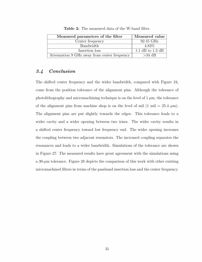
Table 2: The measured data of the W-band filter.
Measured parameters of the filter Measured valueCenter frequency 92.45 GHz
Bandwidth 4.83%Insertion loss 1.1 dB to 1.3 dB
Attenuation 9 GHz away from center frequency >34 dB
3.4 Conclusion
The shifted center frequency and the wider bandwidth, compared with Figure 24,
come from the position tolerance of the alignment pins. Although the tolerance of
photolithography and micromachining technique is on the level of 1 µm, the tolerance
of the alignment pins from machine shop is on the level of mil (1 mil = 25.4 µm).
The alignment pins are put slightly towards the edges. This tolerance leads to a
wider cavity and a wider opening between two irises. The wider cavity results in
a shifted center frequency toward low frequency end. The wider opening increases
the coupling between two adjacent resonators. The increased coupling separates the
resonances and leads to a wider bandwidth. Simulations of the tolerance are shown
in Figure 27. The measured results have great agreement with the simulations using
a 30-µm tolerance. Figure 28 depicts the comparison of this work with other existing
micromachined filters in terms of the passband insertion loss and the center frequency.
31
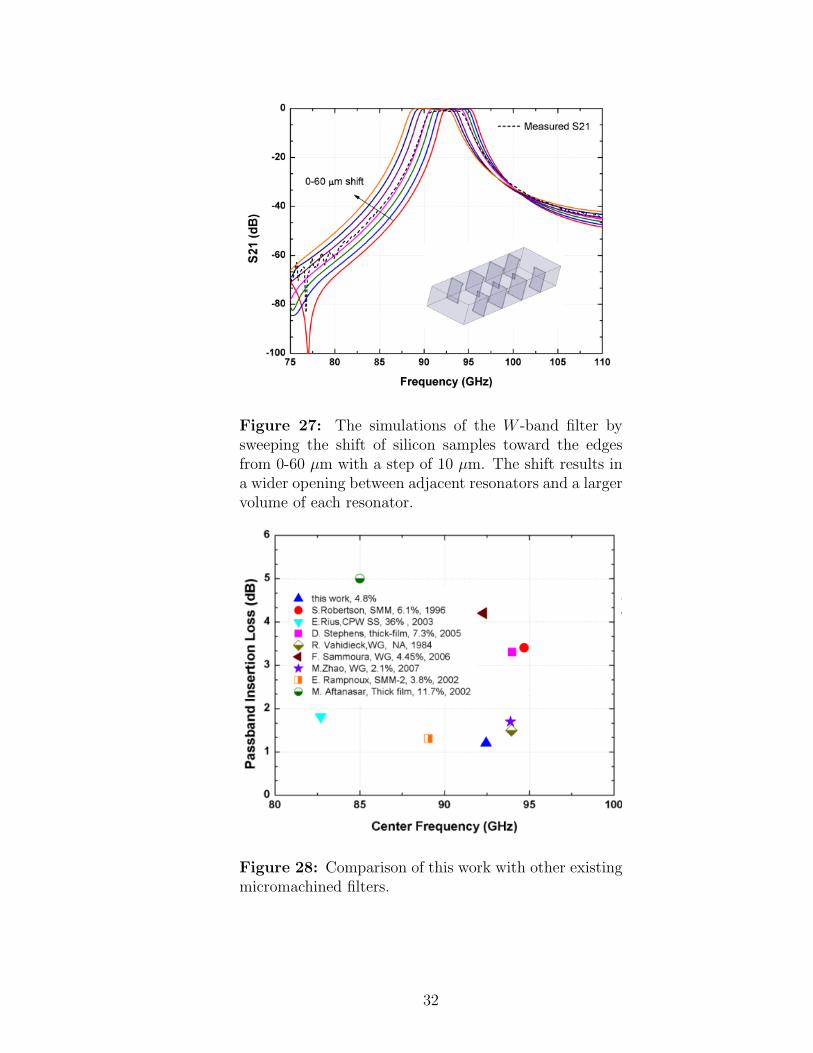
Figure 27: The simulations of the W -band filter bysweeping the shift of silicon samples toward the edgesfrom 0-60 µm with a step of 10 µm. The shift results ina wider opening between adjacent resonators and a largervolume of each resonator.
Figure 28: Comparison of this work with other existingmicromachined filters.
32

CHAPTER IV
A W -BAND HYBRID COUPLER AND A W -BAND
POWER DIVIDER
In this chapter, a silicon micromachined W -band hybrid coupler and a power divider
using the deep reactive ion etching technique are presented. They are designed in
the H-plane of a rectangular waveguide. The hybrid coupler has a ridged waveguide
90 ! phase shifter and a joint waveguide. The power divider utilizes a T -shaped con-
figuration. The simulated response and measured response presented in this chapter
show good agreement. Then, the measured combining e"ciency is measured after
cascading the power divider and the hybrid coupler.
Several waveguide couplers and power dividers have been investigated in the lit-
erature. In [50], a waveguide-based H-plane hybrid coupler centered at 11.424 GHz
with 500 MHz bandwidth is reported. In [51], a 10-60-GHz directional coupler is
presented using shielded membrane microstrip lines. In this chapter, the proposed
W -band hybrid coupler and the power divider are presented with 31.6-GHz and 27.12-
GHz frequency range, respectively, when the return loss is greater than 10 dB. The
waveguide circuits presented here can be easily integrated with the transition in [52]
to build a wafer-scale W -band millimeter wave front-end.
4.1 Design of the Hybrid Coupler
The hybrid coupler, shown in Figure 29, has four ports: Port 1 (input), Port 2
(through), Port 3 (coupled), and Port 4 (isolated). The four ports are connected
to the joint waveguide through H-plane bends respectively, except that Port 1 is
connected to a ridged waveguide 90 ! phase shifter first. The resonant frequency f301
33

is accommodated by the joint waveguide and is defined by d and g in Figure 29. The
Equation 4 gives the resonant frequency.
Figure 29: The topology of (a) the hybrid coupler and (b) thepower divider.
fmnp =c0
2%
!(m%
d)2 + (
n%
b)2 + (
p%
g)2 (4)
where d, b, and g are the width, height ,and length of the joint waveguide, and c0 is
the speed of light. The width d is reduced to less than twice of the WR-10 waveguide
width for shifting f301 to higher frequency and achieving a broad bandwidth. The
impact of d is investigated to show the return loss versus frequency in Figure 30.
With an increase of d, the return loss is improved at the low-frequency end, but is
worsened at the high-frequency end. A ridged waveguide 90 ! phase shifter using
inductive irises is designed instead of using a quarter wavelength waveguide. The iris
34

spacing is given in [53].
Figure 30: Simulated return loss vs. frequency with dif-ferent d as well as the phase deviations of ridged waveg-uide 90 ! phase shifter and a quarter waveguide phaseshifter.
4.2 Design of Power Divider
The T -shaped power divider, shown in Figure 31 , can split the signals from Port
2 and obtain two same phase signals at Port 1 and Port 3. The equivalent circuit
of the H-plane waveguide bend includes a shunt inductor with susceptance that is a
function of r [54]. The thickness of the iris is optimized and reported in Figure 31.
As can be seen, the return loss is improved with the decreasing of iris thickness. The
200-µm thick iris is chosen to facilitate the fabrication. The waveguide circuits are
split along the center of the H-plane. Each circuit is formed by two 1-mm thick
silicon samples. The WR-10 waveguide flange is enabled by two silicon samples and
the metal fixture.
The silicon dioxide was deposited on a pre-cleaned double-side polished 1-mm
thick wafer using Unaxis PECVD. A photoresist (PR) mask was used to pattern the
silicon dioxide using plasma thermal ICP. After the removal of residues, the wafer was
35

etched using STS ICP with a depth of 635 µm. Then, the silicon wafer was flipped
and etched from the backside to release the sample. A layer of Ti/Cu/Au is sputtered
on the silicon samples. The two silicon samples of the coupler are shown in Figure 32.
Figure 32 also shows the WR-10 waveguide flange formed by the fixture and silicon
samples.
Figure 31: Simulated return loss against frequency withdi!erent iris thickness.
Figure 32: (a) Silicon blocks of the coupler; (b) WR-10 waveguideflange.
36

4.3 Measurement and Conclusion
The measurements are taken using Agilent 8510 XF VNA. In Figure 33 , the measured
isolation and return loss of the hybrid coupler are greater than 17 dB over 75 to 105
GHz. The average coupling of the hybrid coupler is 3.4 ± 0.4 dB over 85 to 100 GHz.
Figure 33: The S-parameters of the hybrid coupler.
In Figure 34 , the loss of the power divider is 0.6 ± 0.6 dB from Port 2 to Port 1
over 75 to 105 GHz; the return loss is greater than 10 dB over 27.12 GHz [47]. The
dip in the measured S21 at 107 GHz is shifted from the dip out of the W -band at
114 GHz. The frequency shift is caused by the assembly and fabrication tolerances.
The hybrid coupler and the power divider are cascaded to measure the combining
e"ciency at Port 3 of the hybrid coupler, shown in Figure 35. An Agilent signal
generator 8362B and an Agilent source module 83558A are used to generate W -band
signals that are fed into Port 2 of the power divider. The split signals are fed into
Port 1 and Port 4 of the hybrid coupler. An Agilent power sensor W8486A and power
meter E4419B are used to measure the power at Port 3 of the hybrid coupler. The
e"ciency is reported in Figure 35 after calibrating out the loss of the power divider
37

and the metal waveguide bends. The measured combining e"ciency is greater than
80% between 85 GHz and 105 GHz. The low combining e"ciency above 105 GHz
comes from the dip in Figure 34 at 107 GHz. The dip in Figure 34 at 107 GHz
comes from the dip at 114 GHz, which is out of the interested frequency band. The
tolerances in the fabrication and assembly lead to the frequency shift to the lower
frequency end.
Figure 34: The S-parameters of the power divider.
38

Figure 35: The measured combining e"ciency after cas-cading the power divider and hybrid structure.
39

CHAPTER V
A WIDEBAND COPLANAR WAVEGUIDE TO
RECTANGULAR WAVEGUIDE TRANSITION
Communication and satellite systems are seeking a fully integrated solution where
waveguide components can be accessed through planar circuit board circuits such
as printed microstrip and coplanar waveguide lines. Some intrinsic obstacles in this
integration e!ort can be tackled through reconciling many fundamental di!erences
that exist between planar and waveguide transmission lines. A rectangular waveguide
has the advantages of low loss and high power capacity. The traditional rectangular
waveguide at low frequencies , however, is bulky and is not suitable for the system-on-
chip integration. Nevertheless, the size of rectangular waveguides shrinks dramatically
in the millimeter-wave and submillimeter-wave frequency ranges [55]. Meanwhile, the
loss of other compact planar transmission lines, such as microstrips, keeps increasing
when the operating frequency goes up. The integration of sub-systems into a packaged
solution with a combination of planar and waveguide components provides advantages
in terms of high performance and reduced size. For this reason, it is crucial to building
an understanding of planar-to-waveguide transition structures and their application
in microwave component designs at millimeter-wave frequencies.
5.1 Existing CPW-to-Waveguide Transitions
In the existing approaches, transitions [55] [56] [57] with conventional machining
techniques are not easily adopted by the micromachining, which is feasible for the
integration of submillimeter-wave circuits, shown in Figure 36. The transitions from
planar waveguides to substrate-integrated rectangular waveguides are reported [59]
40
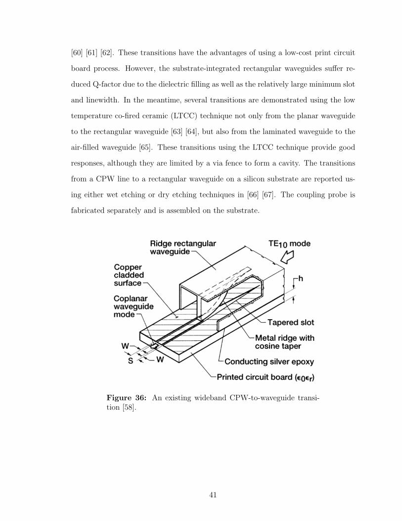
[60] [61] [62]. These transitions have the advantages of using a low-cost print circuit
board process. However, the substrate-integrated rectangular waveguides su!er re-
duced Q-factor due to the dielectric filling as well as the relatively large minimum slot
and linewidth. In the meantime, several transitions are demonstrated using the low
temperature co-fired ceramic (LTCC) technique not only from the planar waveguide
to the rectangular waveguide [63] [64], but also from the laminated waveguide to the
air-filled waveguide [65]. These transitions using the LTCC technique provide good
responses, although they are limited by a via fence to form a cavity. The transitions
from a CPW line to a rectangular waveguide on a silicon substrate are reported us-
ing either wet etching or dry etching techniques in [66] [67]. The coupling probe is
fabricated separately and is assembled on the substrate.
Figure 36: An existing wideband CPW-to-waveguide transi-tion [58].
41
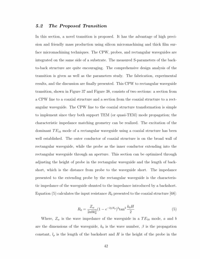
5.2 The Proposed Transition
In this section, a novel transition is proposed. It has the advantage of high preci-
sion and friendly mass production using silicon micromachining and thick film sur-
face micromachining techniques. The CPW, probes, and rectangular waveguides are
integrated on the same side of a substrate. The measured S-parameters of the back-
to-back structure are quite encouraging. The comprehensive design analysis of the
transition is given as well as the parameters study. The fabrication, experimental
results, and the discussion are finally presented. This CPW to rectangular waveguide
transition, shown in Figure 37 and Figure 38, consists of two sections: a section from
a CPW line to a coaxial structure and a section from the coaxial structure to a rect-
angular waveguide. The CPW line to the coaxial structure transformation is simple
to implement since they both support TEM (or quasi-TEM) mode propagation; the
characteristic impedance matching geometry can be realized. The excitation of the
dominant TE10 mode of a rectangular waveguide using a coaxial structure has been
well established. The outer conductor of coaxial structure is on the broad wall of
rectangular waveguide, while the probe as the inner conductor extending into the
rectangular waveguide through an aperture. This section can be optimized through
adjusting the height of probe in the rectangular waveguide and the length of back-
short, which is the distance from probe to the waveguide short. The impedance
presented to the extending probe by the rectangular waveguide is the characteris-
tic impedance of the waveguide shunted to the impedance introduced by a backshort.
Equation (5) calculates the input resistance R0 presented to the coaxial structure [68]:
R0 =Zw
2abk20
(1" e"2j"lp)2tan2 k0H
2(5)
Where, Zw is the wave impedance of the waveguide in a TE10 mode, a and b
are the dimensions of the waveguide, k0 is the wave number, ( is the propagation
constant, lp is the length of the backshort and H is the height of the probe in the
42
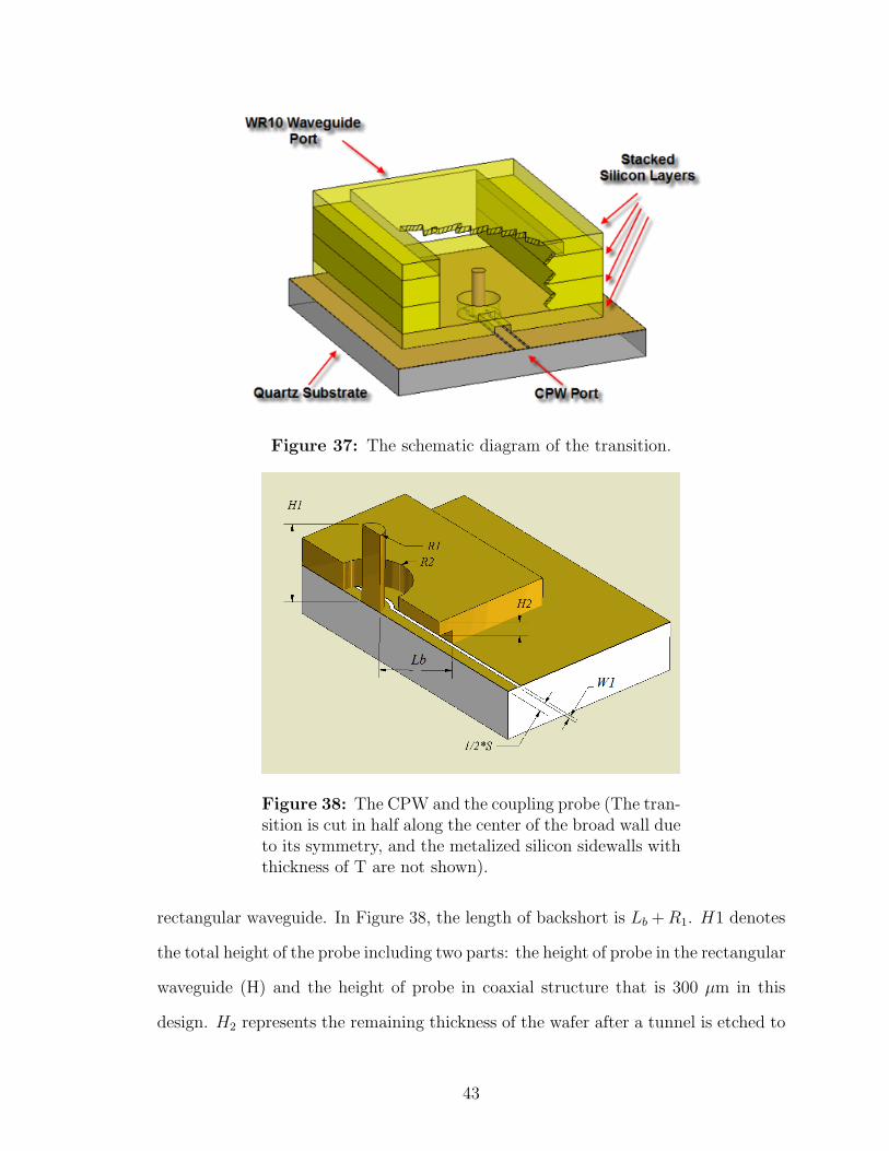
Figure 37: The schematic diagram of the transition.
Figure 38: The CPW and the coupling probe (The tran-sition is cut in half along the center of the broad wall dueto its symmetry, and the metalized silicon sidewalls withthickness of T are not shown).
rectangular waveguide. In Figure 38, the length of backshort is Lb + R1. H1 denotes
the total height of the probe including two parts: the height of probe in the rectangular
waveguide (H) and the height of probe in coaxial structure that is 300 µm in this
design. H2 represents the remaining thickness of the wafer after a tunnel is etched to
43

accommodate the CPW feeding. R1 is the radius of the probe. S is the width of the
inner conductor of the CPW line. W1 is the width of the CPW slots.
5.3 Optimization of the Transition
The initial values of H and the length of the backshort can be determined through
matching the impedance from the coaxial structure to the rectangular waveguide.
This design rule initially gives the height of the probe in rectangular waveguide over
half of the waveguide height. This configuration is hard to implement due to the
aspect-ratio limit in fabrication. The height of a standard WR-10 waveguide is 1.27
mm and half of it is over 600 µm. The total height of the probe, H1, will be close to 1
mm, including the coaxial part. To get a su"ciently good impedance matching while
using a relatively short probe, the aperture radius on the broad wall is used as an
additional design variable. Decreasing the probe height in rectangular waveguide is
equivalent to reducing the coupling between the probe and the waveguide. Di!erent
from the current probe transition in [62], an impedance transformation is taken into
account [69]. This open-circuited probe transition is suitable for wideband design [70].
To compensate for the mismatching over wide bandwidth, a short-end CPW stub is
introduced, which improves the transition and provides another tuning variable in the
whole transition. Meanwhile, to reduce the reflection back into the coaxial structure,
the aperture radius, i.e. the radius of the outer conductor of the coaxial structure, is
increased to reduce the capacitive coupling between the inner conductor and the outer
conductor. Consequently, it increases the characteristic impedance of the coaxial
structure and thus changes the impedance matching of the transition. However, if
the length of the coaxial structure is small compared to the guided wavelength, the
reflection introduced in the coaxial structure only plays a minor role and can be tuned
by other design variables. In this design, the length of the coaxial section is optimized
to 315µm, which is approximately one tenth of the wavelength at the center operating
44

frequency. The standard WR-10 (2.54mm by 1.27mm) waveguide has been used in
the transition design which is optimized over the whole of W-band. The optimized
dimensions are listed in Table 3.
Table 3: Dimensions of the transition
Dimensions Value in µmH1 850H2 150R1 115R2 400W1 40S 240Lb 1000
In [69], an equivalent circuit model is used to explain a waveguide probe with a load
at one end. In this work, the CPW tuning stub and the backshort are used to achieve
wideband transition. The CPW tuning stub is shunted to the coaxial structure with
characteristic impedance. The transformation provided by the transformer depends
on the probe height and the o!set [82]. The probe in the waveguide can be modeled
as a series LC circuit. The waveguide backshort can also be represented by a shunt
transmission line connected with the waveguide impedance. Although the standard
WR-10 dimensions are used in this section, this approach can be generalized to other
rectangular waveguide cross-sections. The probe height, the aperture radius, the
length of the tuning stub, and the coaxial structure length are optimized to tune the
impedance matching. The height of the probe will a!ect not only the capacitance and
the inductance, but also the transformer. The coaxial section length is simulated using
the constant probe height in the rectangular waveguide. The results are presented in
Figure 39 and Figure 40.
The standard WR-10 waveguide dimensions (2.54mm by 1.27mm) are utilized for
the cross section of the rectangular waveguide. The silicon layer with a coax structure
is patterned on a 300-µm thick wafer. The CPW line is fabricated on top of a quartz
45
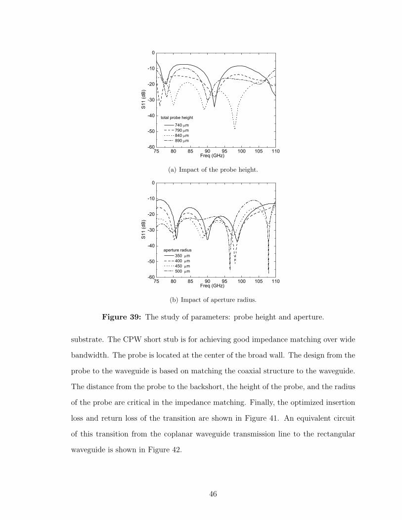
75 80 85 90 95 100 105 110-60
-50
-40
-30
-20
-10
0
740 !m 790 !m 840 !m 890 !m
S11
(dB
)
Freq (GHz)
total probe height
(a) Impact of the probe height.
75 80 85 90 95 100 105 110-60
-50
-40
-30
-20
-10
0
350 !m 400 !m 450 !m 500 !m
S11
(dB
)
Freq (GHz)
aperture radius
(b) Impact of aperture radius.
Figure 39: The study of parameters: probe height and aperture.
substrate. The CPW short stub is for achieving good impedance matching over wide
bandwidth. The probe is located at the center of the broad wall. The design from the
probe to the waveguide is based on matching the coaxial structure to the waveguide.
The distance from the probe to the backshort, the height of the probe, and the radius
of the probe are critical in the impedance matching. Finally, the optimized insertion
loss and return loss of the transition are shown in Figure 41. An equivalent circuit
of this transition from the coplanar waveguide transmission line to the rectangular
waveguide is shown in Figure 42.
46
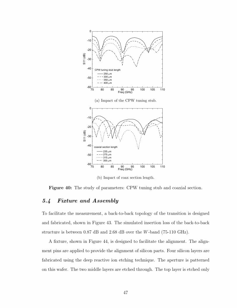
75 80 85 90 95 100 105 110-60
-50
-40
-30
-20
-10
0
S11
(dB
)
Freq (GHz)
250 !m 300 !m 350 !m 400 !m
CPW tuning stub length
(a) Impact of the CPW tuning stub.
75 80 85 90 95 100 105 110-60
-50
-40
-30
-20
-10
0
S11
(dB
)
Freq (GHz)
235 !m 275 !m 315 !m 355 !m
coaxial section length
(b) Impact of coax section length.
Figure 40: The study of parameters: CPW tuning stub and coaxial section.
5.4 Fixture and Assembly
To facilitate the measurement, a back-to-back topology of the transition is designed
and fabricated, shown in Figure 43. The simulated insertion loss of the back-to-back
structure is between 0.87 dB and 2.68 dB over the W -band (75-110 GHz).
A fixture, shown in Figure 44, is designed to facilitate the alignment. The align-
ment pins are applied to provide the alignment of silicon parts. Four silicon layers are
fabricated using the deep reactive ion etching technique. The aperture is patterned
on this wafer. The two middle layers are etched through. The top layer is etched only
47

Figure 41: The simulated insertion loss and return lossof the transition.
ZW( )
L2
Cc
C2
ZCPW
CPW tuning stub RWG backshort
Extending probe
T:1
Zc
Figure 42: The equivalent of this transition.
220 µm deep with the pattern of the rectangular waveguide and released from the
back. Finally, the four silicon layers form a rectangular waveguide with a 1.27 mm
height. The metalized probe and the CPW line are fabricated on a quartz substrate.
A picture of the fixture and the stacked samples are shown in Figure 44.
The first step of the silicon substrate preparation is wafer cleaning. Then, pho-
toresist SRP220 is spun and patterned on the top of the silicon wafer. The patterned
wafer is baked for 5 minutes, before the STS ICP is applied to etch the topside to the
desired depth. A clean process is utilized to clean the photoresist residues from the
48

Figure 43: The back-to-back transition.
(a) The fixture, quartz substrate and sil-icon samples.
(b) The device under test.
Figure 44: The fixture and the device under test.
topside etching. Then, Uniaxis PECVD is used to deposit a thin silicon dioxide layer
to protect the patterned topside. Once the silicon dioxide is deposited, the wafer is
flipped and patterned with a layer of photoresist. Then, the sample is released using
the dry etching. Finally, BOE is applied to remove the silicon dioxide layer. The
silicon samples are metallized using a DC Sputter with a layer of Ti/Cu/Au. The
fabrication flow is shown in Figure 45.
For the fabrication of the open-circuit probe, a Ti/Cu/Ti layer is sputtered and
patterned to open the window for the SU-8 patterning from the backside of the
49

transparent quartz wafer. This improves the SU-8 adhesion to the quartz. An 800
µm negative photo-definable epoxy SU-8 2035 is dispensed uniformly on top of the
quartz. It is patterned under UV to define the mold of the vertical probe. Another
Ti/Cu/Ti layer is sputtered as the seed layer to cover the probes, as well as the
substrate in a conformal manner. Then, the negative photoresist NR9-8000 is coated
and patterned in a non-contact way to cover the CPW slot region. The copper and
gold layers are electroplated to cover the sidewall of the probe, as well as the exposed
ground feeding structures. As the final step, the photoresist NR9-8000 and the seed
layer are removed one by one to release the structure. The fabrication flow is shown
in Figure 45. Figure 46 gives the SEM images of the probe and the aperture on a
300-µm thick wafer.
(a) Silicon process flow. (b) SU-8 process flow.
Figure 45: The fabrication process flow. In (a), the process flow of using the deepreactive ion etching technique is given. In (b), the process of making SU-8 pillar andCPW lines on quartz is provided.
50

(a) SEM photo of the probe. (b) SEM photo of the silicon sample.
Figure 46: SEM photos of the probe and the silicon sample.
5.5 Measurement
The S-parameters measurements of the waveguide transition are taken using an Ag-
ilent Vector Network Analyzer 8510XF. The NIST Multical TRL algorithm is used
to calibrate the measurement system using the HP BASIC. The insertion loss and
the return loss of the back-to-back structure are reported in Figure 47 and Figure 48.
The measured average insertion loss of the back-to-back structure is 2.25dB with 1dB
ripple and the return loss is better than 11 dB over the whole W-band. Compared
to the simulation, the return loss is still higher than the simulated return loss due to
the tolerance in the fabrication and assembly.
5.6 Conclusion
In this chapter, a novel fully micromachined coplanar waveguide-to-rectangular waveg-
uide transition is presented. In the proposed transition, the CPW and the rectangular
waveguide are patterned and integrated on the same side of a substrate, while the
coupling probe is patterned on the substrate instead of being fabricated separately.
These changes make the transition more suitable for RF packaged circuits and easily
extendable to THz applications. The simulated insertion loss of the back-to-back
structure is between -0.87 dB and -2.68 dB and simulated return loss is less than
-16.6 dB over the W -band. The measured average insertion loss of the back-to-back
51
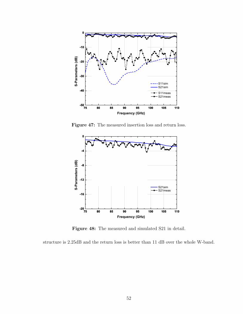
75 80 85 90 95 100 105 110-50
-40
-30
-20
-10
0
75 80 85 90 95 100 105 110-50
-40
-30
-20
-10
0
S11meas S21meas
S-Pa
ram
eter
s (d
B)
Frequency (GHz)
S11sim S21sim
Figure 47: The measured insertion loss and return loss.
75 80 85 90 95 100 105 110-20
-16
-12
-8
-4
0
75 80 85 90 95 100 105 110-20
-16
-12
-8
-4
0
S21measS-Pa
ram
eter
s (d
B)
Frequency (GHz)
S21sim
Figure 48: The measured and simulated S21 in detail.
structure is 2.25dB and the return loss is better than 11 dB over the whole W-band.
52

CHAPTER VI
A W -BAND MICROMACHINED CAVITY FILTER
INCLUDING THE NOVEL INTEGRATED TRANSITION
FROM CPW FEEDING LINES
6.1 Design Topology
This chapter proposes a W -band bandpass filter topology, shown in Figure 49, which
consists of two ridge resonator structures coupled to each other. The input and output
ports are produced by a direct coupling that occurs between the transition probe and
the first resonant mode of the structure. The standard WR-10 waveguide dimensions
(2.54mm-1.27mm) are utilized for the rectangular waveguide.
The initial goal is to design a filter with a center frequency at 96.5 GHz and
a fractional bandwidth of 2.6%. The size of the resonant cavity dictates both the
resonant frequency and the proximity of the input and output coupling. In the case
of Chebychev filter, it is advantageous to minimize cross-coupling between the input
and output ports to increase the rejection band of the filter. The separation of
the ports is increasingly critical since the transition probes are located in a central
region inside cavities. The filter can be fully described by the resonant frequencies
of the synchronous resonators with identical dimensions, the coupling factor between
two resonators, and the external coupling between the transition probes and the
resonators. A drawing of all layers of the filter is shown in Figure 50.
53

Waveguide Resonators
CPW-WaviguideTransition
Iris
Figure 49: The proposed filter topology.
6.2 Analysis of Coupling and Resonance
The first design step is to analyze the resonance frequency of a cavity with stan-
dard WR-10 dimensions. The resonance frequency is found using the fundamen-
tal equations for rectangular waveguide cavities [68] and is given by Equation (6)
and Equation (7). A standard rectangular waveguide cavity with dimensions 2.54
mm!2.54mm!1.27 mm would resonate at approximately 84 GHz. At this starting
point we are facing the need to reduce the cavity size to increase the resonant fre-
quency while keeping the largest probe separation to guarantee a good level of filter
rejection.
Kmnl =
#
(m%
x)2 + (
n%
y)2 + (
l%
z)2 (6)
54

CPW with PostsExtensions
Transition Layer
Filter Structure
Figure 50: Transition and filter layer.
fres =ckmnl
2%$
)eff(7)
One option is to adopt a ridge cavity design [71] [72] [73] [74] consisting of the
cavity with a solid inclusive block. This gives greater flexibility in the realization
of higher resonant frequencies while increasing the separation of the coupling posts.
The resonator structure is shown in Figure 51. The cavity dimensions are a and b
corresponding to x and z axis. The included metal block has a width W , thickness
t, and length L in the x, z, y orientations respectively. The dimension t (525 µm)
55

is fixed as it corresponds to a silicon wafer thickness. This constrain simplifies the
fabrication process.
b
a
t
w
H
L
Figure 51: The dimensions of the cavity.
An eigenmode solution is conducted to characterize the cavity. The electric field
distribution for the first resonant mode of the structure is shown in Figure 52. The
electric field pattern can be seen with strong longitudinal component along the z axis.
The field components concentrate in the region governed by the presence of the ridge
component and fades with increasing +y. These electric field components are then
used to couple to the probe of the transition placed directly below the ridge. The
end of the waveguide with fading field strength allows the appropriate low coupling
strength to produce a selective narrowband response.
56

zx
y
Figure 52: The E-field plot of the resonator.
In the initial analysis, the height location of the inclusive block is determined with
various combinations of block sizes L and W . The results are shown in Figure 53,
where the resonant frequencies are plotted versus corresponding values of H, the
separation from the top of the block to the ceiling of the waveguide. This procedure
is repeated for varying values of L and W and the resonant frequency is inversely
proportional to the block dimension, shown in Figure 54, respectively. The presence
of the internal block gives the advantages of increasing the cavity dimension along
+y to maximize port separation and still realize the increase in resonance frequency
to the desired 96.5 GHz. In other words, when compared to a standard rectangular
cavity, the current resonator with the internal block reduces the required size of the
resonator needed for a specific center frequency. This size reduction is the advantage
of evanescent mode filters.
The initial iris dimensions are designed by extracting the coupling coe"cient
present between resonators. The coupling coe"cient is found by first placing the
resonators in a weakly coupled configuration with respect to the input and output
ports. The loaded resonant frequencies f1 and f2 are then extracted at di!erent gap
between irises. Figure 54 shows the di!erent coupling coe"cient obtained using the
57
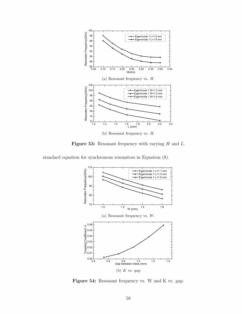
0.05 0.10 0.15 0.20 0.25 0.30 0.35 0.40 0.4586
88
90
92
94
96
98
100
Res
onat
or F
requ
ency
(GH
z)
H(mm)
Eigenmode 1 L=1.6 mm Eigenmode 1 L=1.8 mm
(a) Resonant frequency vs. H.
1.0 1.2 1.4 1.6 1.8 2.0 2.2 2.470
75
80
85
90
95
100
105R
eson
ator
Fre
quen
cy(G
Hz)
L (mm)
Eigenmode 1 W=1.2 mm Eigenmode 1 W=1.4 mm Eigenmode 1 W=1.6 mm
(b) Resonant frequency vs. H.
Figure 53: Resonant frequency with varying H and L.
standard equation for synchronous resonators in Equation (8).
1.0 1.2 1.4 1.670
80
90
100
110
Res
onat
or F
requ
ency
(GH
z)
W (mm)
Eigenmode 1 L=1.1 mm Eigenmode 1 L=1.3 mm Eigenmode 1 L=1.6 mm
(a) Resonant frequency vs. W .
0.4 0.6 0.8 1.0 1.2 1.40.00
0.01
0.02
0.03
0.04
0.05
0.06
Cou
plin
g C
oeffi
cien
t, k
Gap between irises (mm)
(b) K vs. gap
Figure 54: Resonant frequency vs. W and K vs. gap.
58

k =f 2
2 " f 21
f 22 + f 2
1
(8)
where f1 and f2 are the frequency locations of the two resonant poles.
6.3 Implementation and Measurement
The CPW feeding and probes are fabricated on a quartz substrate. A layer of
Ti/Cu/Ti is sputtered and patterned on one side. SU-8 2035 is spun and cured
on top of the substrate. Then, the vertical probes are patterned under the UV light.
To plate the CPW line, another Ti/Cu/Ti layer is sputtered as a seed layer. A layer
of negative photoresist NR9-8000 is coated using the approximate exposure to pattern
the CPW line. An electroplating process is used to plate copper/gold with a thick-
ness of 6µm/2µm to cover the sidewall of the probe. Finally, the seed layer is released
after the negative photoresist NR9-8000 is stripped. Figure 55 shows the CPW line,
probe, and a silicon sample in detail. The deep reactive iron etching (DRIE) tech-
nique is used to fabricate silicon layers, shown in Figure 56 (a). The bottom layer is
made with a 300-µm thick wafer. The two middle layers are fabricated using 525-µm
thick wafers. The top layer is etched only 220-µm deep and released from the back
with di!erent patterns. A photo of the fixture and two middle layers on the quartz
substrate is shown in Figure 56 (b).
Figure 55: (a) The probe and CPW. (b) Silicon layer in detail.
59

(a) (b)
Figure 56: (a) Four silicon layers to form RWG and filter. (b) Twostacked silicon layers on fixture.
The silicon wafer is cleaned and then patterned using the photoresist SRP220.
STS ICP is employed to etch the patterned silicon to the desired depth. Then, the
wafer is cleaned and Unaxis PECVD is used to deposit a thin silicon dioxide layer to
protect the etched topside. Once the silicon dioxide is deposited, the wafer is flipped
and patterned on the backside using SRP220. The silicon sample is released using
STS ICP through etching the wafer from the backside. The diluted HF is used to
remove the silicon dioxide layer. The silicon samples are sputtered using DC-Sputter
for 7-µm thick Ti/Cu/Au layer.
The filter presented in the chapter is simulated using full wave simulator, Ansoft’s
HFSS 10. The quartz substrate has the dielectric constant of 3.78 and the loss tangent
of 0.0002. The metal on the quartz substrate and on the silicon wafers is gold with the
conductivity of 4.1E7 Siemeons/m. The simulation result is reported in Figure 57.
The filter has a center frequency of 96.5 GHz with 2.6% bandwidth. The simulated
insertion loss in the passband is 2.5 dB.
The measurements at W -band are taken using an Agilent Vector Network Analyzer
(VNA) 8510XF. The VNA is calibrated using NIST MultiCal thru-reflect-line (TRL)
algorithm. A pair of probes with 250 µm pitch are used in the measurement. The
measured passband insertion loss is 4.14 dB. The two poles are located at 96.3 GHz
60

85 90 95 100 105 110-50
-40
-30
-20
-10
0
85 90 95 100 105 110-50
-40
-30
-20
-10
0
Simulation
S-P
aram
eter
s (d
B)
Frequency (GHz)
Measurement
Figure 57: Simulation and measurement results of band-pass filterwith transitions.
and 97.1 GHz in the return loss. The measured filter has the center frequency of 96.6
GHz with a bandwidth of 2.9%. Compared to the simulated data with 2.5 dB loss
in the passband, the measured filter has 1.64 dB additional loss. The bandwidth is
increased by 0.3%.
The additional loss may come from the assembly tolerance, the surface roughness
of the silicon waveguide sidewall, and the gap between the layers. The tolerance of
micromachining including DRIE, photolithography and metallization is on the level
of µm or less in the class 100 cleanroom. However, the tolerance of alignment pins
determined by the machine shop is on the level of mil (1/1000 inch or 25.4µm). To
allow the relaxed tolerance on the alignment pins in the assembly, the holes on the
four layers of silicon samples are made slightly larger than that of the alignment
pins. A rigorous sensitivity analysis of coupled resonator filter can be found [75].
61
Unfortunately, we can not directly use it since the tolerances in the assembly will
a!ect not only the coupling, but also the impedance matching of the transition.
The simulation results in Figure 58-Figure 59 show the sensitivity of the response
to the horizontal displacement of the silicon layer having the internal block. y denotes
the displacement along the CPW lines. x denotes the displacement in perpendicular
to the CPW lines. The filter is simulated while sweeping the displacement along y and
x. The simulation shows the filter response is very sensitive to the displacement in
parallel to the CPW line since the electric field is changed in this direction through the
presence of the probe that is right below the block and close to the edge. To reduce the
loss from assembly, a non-standard waveguide with less height will be helpful. It will
not only reduce the necessitated layers, but also simplify the transition design since
the waveguide impedance is proportional to the height. An alternative solution is to
adopt the pin-free alignment method. For applications with an operating frequency
higher than W -band, or even in the THz range, a shorter wavelength makes the
stacking approach easier because fewer silicon layers are needed.
The surface roughness on waveguide sidewalls comes from the deep reactive ion
etching process. The surface roughness, although hard to avoid, can be further re-
duced by adjusting the fabrication parameters, such as the power, time and flow rate
of the gases in the etching and passivation cycles. Another possible reason for the ad-
ditional loss is the gap between the stacking wafers. Instead of cutting the waveguide
along the center of the broad wall, the stacking technique may break current along
the sidewall if a gap exists. In our experiment, a metal cover with four screws is used
to tight the stacking wafers up. In the future, the thermal bonding technique can be
employed to prevent the gap.
62

92 94 96 98 100 102-50
-40
-30
-20
-10
0
a. δy=50,-50um, δx=-50~50umb. δy=25,-25um, δx=-50~50umc. δy=0um, δx=-50~50um
S-P
aram
eter
s (d
B)
Frequency (GHz)
c
a
b
Figure 58: Simulated filter with transitions response versus frequencywhen the second silicon layer undergoes displacement.
6.4 Conclusion
This chapter presents a novel CPW to rectangular waveguide transition as an en-
abling structure for the integration of a W -band filter [76]. The proposed transition
has several advantages: the CPW and the rectangular waveguide are patterned and
integrated on the same side of the substrate; the coupling probe is patterned on the
substrate instead of being fabricated separately. These advantages make the transi-
tion more suitable for RF packaged circuits and easily extendable to THz applications
compared to the existing approaches. The metalized probes in the proposed filter de-
sign are adopted to couple the signal from the CPW line to the waveguide resonant
cavities of a 2-pole filter and eliminate the need for waveguide input/output ports.
The measured filter response agrees well with the simulated response.
63

92 94 96 98 100 102-6
-5
-4
-3
-2
-1a. δy=50,-50um, δx=-50~50umb. δy=25,-25um, δx=-50~50umc. δy=0um, δx=-50~50um
S-P
aram
eter
s (d
B)
Frequency (GHz)
c
a
b
Figure 59: The detail in the passband of simulated filter with transi-tions response versus frequency when the second silicon layer undergoesdisplacement.
64
CHAPTER VII
A HIGH-Q CAVITY RESONATOR AND FILTER FOR
RECONFIGURABLE WPAN APPLICATIONS AT 60 GHZ
7.1 Introduction
In this chapter, a novel silicon micromachined high-Q cavity resonator at 60 GHz
is presented. The concept of the proposed high-Q resonator is introduced first. The
novel realization of the cavity resonator is demonstrated through silicon micromachin-
ing techniques. Full-wave simulations are conducted to verify the propagation mode
and the resonant frequency. The resonant frequency of the cavity resonator can be
tuned through changing the length of a planar stub shunted to a current probe in the
cavity. Experimental results validate the simulation and show great Q factors which
are over 320 at the resonances for the wireless personal area network applications.
A high-Q resonator is highly valued in reconfigurable wireless communication
systems. The cavity resonator [77]- [80] has the intrinsic superior quality factor and
power handling capacity over its planar counterparts, e.g. microstrip resonators and
coplanar waveguide resonators.
However, the resonant frequency of the cavity resonator is traditionally tuned
either by mechanically inserting a screw [81] or by adjusting the gap between a ca-
pacitive post and the ceiling of the cavity through piezoelectric materials [82], shown
in Figure 60, or mechanical force [83]. These methods are di"cult to integrate with
monolithic microwave circuits and are not feasible for low-cost wireless personal area
network applications at 60 GHz.
In the last two decades, with the advance of micromachining techniques and fer-
roelectric materials, RF MEMS switches [84] and Barium Strontium Titanate (BST)
65

Figure 60: Existing tunable cavity filter [82].
capacitors are widely used in planar resonators and planar filters. Tunable planar
filters using RF MEMS switches have been presented with third-order intermodula-
tion intercept point over 40 dBm [85] and remarkable reliability of over 100 billion
cycles [86]. The BST-based capacitors have shown great switching time on the nano-
second level [87] and continuous frequency tuning capability. The pin diodes are ex-
tensively utilized in planar circuits and have the advantages of low cost, fast switching
speed and low tuning voltage. Although RF MEMS switches, BST capacitors and
pin diodes have been successfully demonstrated in the integration with planar mono-
lithic microwave circuits either printed on a substrate or elevated in the air with the
support of a membrane, a low Q factor is associated to these planar passives. In
this chapter, a novel high-Q cavity resonator is presented at 60 GHz. The resonant
frequency of the cavity resonator can be tuned by changing the length of a shunt
planar stub. Therefore, the tuning components, RF MEMS switches, BST capacitors
or pin diodes, can be employed to change the electrical length of the stub and to
tune the resonant frequency of the cavity resonator. The successful demonstration of
the cavity resonator will be beneficial to building reconfigurable cavity-based wireless
communication front-ends with high-Q factors at 60 GHz. The concept of the novel
cavity resonator is described first. Then, the realization of resonator is introduced
66
and is verified using full-wave simulation software. The fabrication and assembly of
the resonator is presented shortly. Finally, the experimental results are presented and
discussed.
7.2 Tunable Cavity Resonator Concept
The cavity resonator is enclosed by the metalized substrate, lid, sidewall, and cur-
rent probe. In contrast with the conventional micromachined cavity resonator, this
resonator has a slot on the sidewall next to the current probe. On the substrate, a
planar stub is shunted to the current probe and is isolated from the metalized sub-
strate by an encompassed gap. The shunt stub starts from the current probe and
extends out of the boundary of the cavity sidewall. Figure 61 depicts the topology
of the proposed tunable cavity resonator. The conventional cavity resonator has the
resonant frequency determined through Equation (9).
fmnp =c0
2%$
)r
!(m%
d)2 + (
n%
b)2 + (
p%
g)2 (9)
where d, b and g are the width, height and length of the cavity resonator respec-
tively, c0 is the speed of light and )r is the dielectric constant of the cavity filling.
The resonant frequency of this resonator is primarily determined by the volume en-
closed by the sidewall and the current probe when the slot is small and the current
probe is close to the slot. The slot, the current probe and the shunt stub serve as a
perturbation of the cavity resonator. The resonance frequency shift comes from the
susceptance change induced by the length of the shunt planar stub. The resonant
frequency of the cavity resonator decreases when the length of the shunt planar stub
increases.
67

Figure 61: The proposed tunable cavity resonator.
7.3 Micromachined Realization
The proposed cavity resonator is very attractive for reconfigurable applications. In
this chapter, three shunt planar stubs with di!erent lengths demonstrate three dif-
ferent resonant frequencies. The electric field distribution of the fundamental TE101
mode in the cavity is simulated using Ansoft’s HFSS and the result is shown in Fig-
ure 62.
The cavity resonator is fed through coplanar waveguide (CPW) transmission lines
which are deposited on top of the substrate. These two feed lines enter the cavity
through two openings on the sidewalls next to the sidewall with a slot. They are
weakly coupled to the resonator for accurately extracting the unloaded quality fac-
tor from the resonant response. To validate the concept, a micromachined cavity
resonator is designed at 60 GHz for WPAN applications, shown in Figure 63. The
dimensions of the tunable resonator are presented in Table 4. The resonant frequency
68

Figure 62: The E-field of the cavity resonator.
is tuned by the length change of Xt. Three resonators are made with same dimen-
sions, except Xt, to show the frequency tuning. The ’state 1’ of the resonator denotes
that Xt is 600µm; the state 2 that Xt is 800µm; the state 3 that Xt is 1000µm. Fig-
ure 64 gives the implementation of this tunable cavity resonator using micromachined
techniques.
Table 4: Dimensions of the proposed resonator
Variable Vaule(µm) Variable Vaule(µm)S1 240 Y f 1900W1 35 Y s 1000S2 120 Y i 1780W2 35 R 60Xc 3600 Hc 310Y c 3560 Xt 600(state 1)G1 400 Xt 800(state 2)G2 60.58 Xt 1000(state 3)Hs 60.58
The lid, the sidewalls and the current probe are made by using a micromachined
69

Figure 63: The dimensions of the cavity.
silicon sample. The shunt stub and two CPW feed lines are deposited on a quartz
wafer. The whole cavity is formed by bonding the silicon sample to the quartz wafer.
To ease fabrication, the height of the cavity is chosen to be 310 µm. A higher quality
factor can be reached by increasing the height of the cavity.
7.4 Implementation and Assembly
The entire resonator is built using micromachining techniques on a quartz wafer and
on a silicon wafer. The quartz wafer used in this chapter has an 1-inch diameter,
which is big enough for two dies, one die for each resonator, shown in Figure 65. The
two dies on one quartz wafer have same dimensions except the length of Xt.
A quartz wafer was cleaned first with Acetone. A photoresist layer was spun
and patterned on top of the quartz wafer. A lift-o! process was carried out by
using electrical beam evaporator to achieve a metal layer, Ti/Cu/Au, with a total
70

Figure 64: The implementation of the cavity.
Figure 65: Quartz wafer with two dies, the right oneassembled with silicon sample.
71

thickness of 3 µm. The lift-o! process improved the surface roughness of the metal
layer compared to electroplating. The metal layer that had the CPW feeds and shunt
stub on it served also as the metal bottom of the cavity. The alignment pillars were
made on top of the metal layer using negative photoresist SU-8 with a height of 150
µm. These alignment pins were used to accurately align the silicon sample on the
quartz wafer. In Figure 65, the silicon sample was assembled on the right die.
The silicon sample shown in Figure 65 was made using deep reactive ion etching
techniques. More than twenty silicon samples were obtained from one four-inch wafer.
First, a photoresist layer was spun and patterned on the silicon wafer to form a mask
for deep etching. An inductive coupled plasma tool, STS ICP, was used for deep
etching. After removal of the photoresist residue, a thin silicon dioxide layer was
prepared as a stop layer for the backside etching. Then, the etched wafer was flipped,
patterned, and etched from the backside to release the silicon sample. The DC-sputter
was used to put down a 3-µm layer of Ti/Cu and a 100-nm layer of Au on the cavity
side after the removal of the photoresist residue and the thin silicon dioxide layer.
The SEM picture of the silicon sample in Figure 66 was taken using a Hitachi 3500H
SEM. The height of the cavity was measured using a Tencor KLA Profilometer. A
four-degree re-entrant angle on the sidewall from the deep etching is noticed in the
SEM image. The cavity volume is increased and the resonant frequency is decreased
due to the re-entrant angle. Finally, the silicon sample and the quartz wafer were
assembled together and mounted on a fixture to prevent the air gap between them.
7.5 Experiment and Discussion
The measurements of the tunable cavity resonator were taken using an Agilent Vector
Network Analyzer (VNA) 8510XF and GGB probes with 250-µm pitch. The Short-
Open-Load-Thru (SOLT) calibration method was used to calibrate the VNA to the
probe tips. The measured resonant frequency of the resonator at each state, shown
72

Figure 66: SEM picture of the silicon sample.
in Figure 68, has very good agreement with the simulated results. Ansoft’s HFSS
is used in the simulation, where the conductivity of the copper is 5.8!10E7 S/m,
the loss tangent of the quartz wafer is 7!10E4, and a four-degree re-entrant angle
is included. The loaded Q and unloaded Q of the resonator are calculated using the
equations in [80] and reported in Table 5. The measured unloaded Q is 328 at ’state
1’, 368 at ’state 2’ and 356 at ’state 3’, which are lower than those in the simulation
shown in Figure 67 and Figure 68. This is probably due to the surface roughness of
the cavity. However, the concept of the cavity resonator with the resonant frequency
a!ected by a current probe and a planar stub with an additive length is validated
with Q over 320. The summary of the measured and simulated values are reported
in Table 5.
Table 5: Simulated and measured resonant frequency and unloaded Q.
State Simulation State Measurementf0 Ql Qu f0 Ql Qu
1 60.58 336 395 1 60.44 298 3282 59.77 379 453 2 59.69 331 3683 59.23 376 448 3 59.27 316 356
73

Figure 67: Simulation of the cavity resonator.
Figure 68: Measurement of the cavity resonator.
7.6 Conclusion
In this chapter, a novel cavity resonator with a current probe and a planar shunt stub
is presented. The proposed cavity resonator scheme provides the opportunity of using
planar tuning components, RF MEMS switches, BST capacitor or pin diodes, to build
74

reconfigurable wireless communication systems based on a cavity-based resonator that
has intrinsically high-Q factor over its planar counterparts. The measured resonant
response shows great agreement with the simulation results. The measured unloaded
Q is over 320 for all three states at the resonant frequencies around 60 GHz.
75
CHAPTER VIII
A BROADBAND 900-GHZ SILICON MICROMACHINED
TWO-ANODE FREQUENCY TRIPLER
8.1 Introduction
Terahertz (THz) signal sources in the 100 GHz to 10 THz have attracted scientific
interests over several decades for both terrestrial and astronomical applications [5].
The abundant THz radiation that bathes our universe contains a wealth of scientific
information, such as, the dynamic properties of a wide range of molecules on planets
in our solar system as well as in remote regions of the universe. The spectroscopic
signatures of such molecules allow scientists to build dynamical models that help
to better our understanding of the universe. The investigation of the correlation
between the shape of the ozone hole and the distribution of chlorine monoxide tackles
the puzzle of how human activities a!ect the health of our planet [88].
A superheterodyne radiometer is a crucial instrument for conducting quantitative
spectroscopy on space missions. An important component in such instruments is the
THz signal source used to pump mixers in a superheterodyne radiometer. THz signal
sources that are compact, highly e"cient, broadband and low-cost are extremely
desirable. A couple of decades ago, tube-type THz signal sources, known as the gas-
filled and vacuum tube, including backward wave oscillator, gyrotron, klystron, and
far-infrared laser, were intensively studied [89], [90].
Solid-state devices provide a compact and lightweight solution for generating THz
radiation. Although rapid advance has been made in HBV diodes [91], [92], [93]
and three-terminal solid-state devices such as high electron mobility transistors [94]
76
and heterojunction bipolar transistors [95], GaAs Schottky diodes still provide un-
surpassed performance advantage and are widely used in the THz frequency multi-
pliers [5], [96], [97].
Schottky diode chips are nominally housed in waveguide based circuits to pro-
vide appropriate input and output matching conditions along with providing a well
understood radiatin mode. Normally, these waveguide circuits and their fixtures are
fabricated with the use of direct machining, including high precision lathes and milling
machines and they have been demonstrated up to approximately 2 THz [98]. However,
as the desired wavelength is increasingly small in the THz band, the small dimen-
sions make these waveguide circuits di"cult or impossible to fabricate and the cost
of fabrication often becomes prohibitive in direct machining. The direct machining
process is also constrained by the diameter of milling tools that lead to round corners.
An example of direct machining is a 2.5 THz corrugated horn that is reported in [99]
with the miniature being 27µm!105µm. Other direct machined waveguide circuits
include frequency multipliers [91], [100] and power combining circuits [101], [102].
Besides direct machining, many other techniques have also been proposed to
provide low-loss and low-cost solutions for the fabrication of THz waveguide cir-
cuits [99], [103]. Electroforming relies on electroplating to form a metal layer onto a
mandrel in a plating bath. The metal layer is eventually built up in the bath and
an independent shape forms. The mandrel is then burned out, leaving the expected
metal waveguide structures. The electroforming process is suitable for producing com-
plex waveguide structures, but the process is fairly time consuming and requires a
high-precision mandrel first. An example of electroforming is a 2.5 THz horn reported
in [104] with the use of a standard copper electroforming process.
Surface micromachining with the use of thick photoresists, such as, SU-8, to build
the structure of THz wavguides has also been reported [105]. A thick photoresist layer
can be spun and patterned for a thickness of up to 1-2 mm. The developed SU-8 is then
77
metalized to form waveguide structures. The fabrication of SU-8 is relatively simple,
but has a long baking and curing time determined by the height of the structures.
The uniformity of the height over a large area, e.g. a 4” wafer, is strongly a!ected
by the baking and curing recipe. The direct use of SU-8 as dielectric filling to form a
waveguide structure leads to high loss at THz frequencies. Therefore, SU-8 is suitable
for sidewall structures. Instead of using thick photoresist as a structure layer, metal-
film waveguides use thick photoresist as a sacrificial layer [103]. Once the thick
photoresist structure forms, a thin metal layer is sputtered as a seed layer, followed
by an electroplating process to have a thick metal layer. The thick photoresist is
removed by chemicals, leaving a waveguide structure filled with the air. The metal-
film process is capable of building the full-height waveguides only at the high end
of THz frequencies because of the limit of photoresist thickness. A reduced-height
waveguide horn antenna is reported in [106] at 200 GHz.
Unlike surface micromachining with the use of photo-definedable polymer, a stereo-
lithography technique, extensively studied in the millimeter-wave range, is a 3-D
fabrication method that uses laser beam to cure resin material layer by layer [107],
[108]. The entire waveguide structures are immersed in resin, therefore the stereo-
lithography method is for stand-alone components and is not compatible with the
standard CMOS process. X-ray LIGA is a complex process, allowing to achieve
extremely high-aspect-ratio structures in the positive resist. This process requires a
thick X-ray mask and is an expensive method. X-ray LIGA can produce nearly perfect
geometries. The X-ray LIGA process is introduced in [109] to acheive a 600-700-GHz
backward wave oscillator with the feature size of about 20 microns.
Without using any photoresis or resin, laser beam etching has been proposed
to drive silicon etching using chemical reactions. A laser-assisted chemical etching
system is summarized in [110]. The Cl2 gas is used to accelerate the etching process.
The laser beam etching method is capable of achieving highly complex 3-D structures
78

in a small area of several square millimeters. This method is time consuming to
etch a chunk of silicon substrate because it is a process in series and a layer of 1-2
µm thick silicon is usually removed along with the moving of the laser beam. The
fabrication of laser beam etching requires a blank wafer to avoid the contamination
of the etching chamber and the corrosive e!ect of ambinet Cl2. In [111], a 2-THz
waveguide structure is reported using the laser beam chemical etching technique at
the University of Arizona. This technique also becomes problematic for the lower
THz range where feature sizes can be relatively large.
The wet etching of silicon is a simple technique and has been widely used in
waveguides [112], filters [113], antennas [114], and mixers [115]. However, the design
is limited by the crystal orientation of silicon substrates and accurate dimensional
control is also di"cult. Deep reactive ion etching technique is a dry etching technique
that is powered by inductively coupled high-density plasma and can achieve a high
aspect ratio up to 20:1. This technique has been used in a wide range of millimeter-
wave components, including the finite coplanar line-to-waveguide transition [116] and
the waveguide hybrid junction [117]. For the submillimeter-wave passives, a 400-
GHz straight waveguide [118] and a 325-500-GHz quadrature hybrid with waveguide
structures [119] were reported. For THz signal sources, a silicon micromachined
waveguide multiplier using the heterostructure barrier varactor was reported at 261
GHz in [120]. A 600-GHz mixer using both wet and dry etching was presented in [121].
The purpose of this study is to investigate the feasibility of using the deep reac-
tive ion etching technique as an enabling integration method to build THz frequency
multipliers at 900 GHz. Initially developed in the semiconductor industry, the deep
reactive ion etching technique is friendly to mass production, inherently suitable for
high-precision design, indiscriminately attainable to all types of silicon substrates with
di!erent doping and crystal orientations. The waveguide passives fabricated using this
technique have the intrinsic properties of low-loss, high-Q, and high power handling
79

capacity. In this study, a broadband 900-GHz silicon micromachined frequency tripler
using a pair of Schottky diodes in the balanced configuration is successfully demon-
strated for the first time. The outline of the remaining chapter is as follows: Section
II introduces the circuit design. Section III describes the fabrication and assembly
of the compact waveguide circuits. The measurement and analysis are presented in
Section IV, and finally, conclusion is given in Section V.
8.2 Circuit Design
8.2.1 Design Methodology
The 900 GHz tripler chip utilizes topology shown in Figure 69 and previously reported
in [122], [123], [124]. As in [122], monolithically integrated input and output probes
have been added to simplify assembly. Mettalic on-chip beamleads allow for the
mounting and handling of the chip inside the waveguide block.
Since 1990s, the advance of full-wave electromagnetic simulators, e.g. Ansoft’s
HFSS, and nonlinear circuit simulators, e.g. Agilent’s ADS, have greatly aided in the
design of broadband multipliers. Pioneered by [123], the simulation was performed
with the ever increasing accuracy and speed, thanks to the rapid progress of both
software and the hardware. Passive 3-D structures and discontinuities are simulated
and de-embeded using full-wave simulators and the optimized S-parameter files are
extracted. The S-parameter files are imported into ADS to optimize the performance
of frequency multipliers for maximizing output power and conversion e"ciency with
the use of electrical and physical parameters of Schottky diodes.
The waveguide structure of the tripler is split in half along the E-plane center
and the two half blocks have the mirrored patterns. The GaAs chip with metal
beamleads is mounted onto the micromachined waveguide chip channel. The diodes
in this design are self-biased and thus do not require a dc biasing scheme, though , the
metal beamleads provide RF ground for the circuit in this design. The two anodes are
80

Input E-plane probe
Channel wall (ground)
Output waveguide
Output backshort
Input waveguide
Input backshort
Input matching network Output
E-plane probe
Ef1 E3f1
E field
Currents
f1 2f1 3f1
Figure 69: Block diagram of a 2-anode 900 GHz balanced tripler. The tripler usesa split-block waveguide design. The diodes are connected in series at dc and arein a balanced configuration at RF. The chip is inserted in a channel between theinput and the output rectangular waveguides. An E-plane probe located in the inputwaveguide couples the signals at the fundamental frequency to a suspended microstripline that can propagate only in a quasi-TEM mode. This line has several sections oflow and high impedances used to match the diodes at the input and output frequencyand to prevent the third harmonics from leaking into the input waveguide. The thirdharmonic produced by the diodes is coupled to the output waveguide by the second E-plane probe. Additional waveguide sections of di!erent impedances and lengths (notshown) are used for the input and output matching. !Ef1 and !E3f1 stand respectivelyfor the electric field at the fundamental frequency f1 and at the output frequency3!f1. The electric fields and the current lines are represented for the fundamentalfrequency f1 (thick light lines), the idler frequency 2!f1 (dashed lines) and the outputfrequency 3!f1 (light plain lines)
used in the anti-parallel configuration [124], enabling the generated odd harmonics
to flow toward the same direction as the RF ground. The generated even harmonics
proceed towards the opposite direction and are trapped in a virtual loop that consists
of the two paths from the suspended microstrip line to the RF ground. Figure 70
shows this anti-parallel configuration, the virtual loop for the even harmonics, and the
81
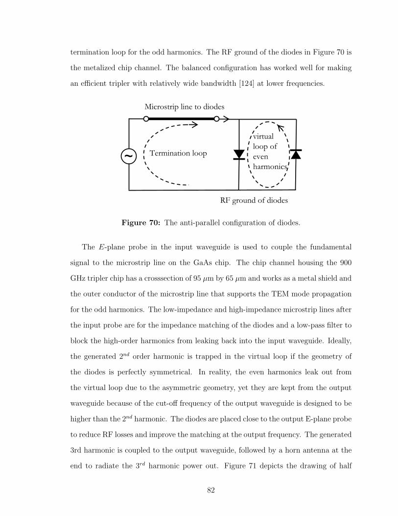
termination loop for the odd harmonics. The RF ground of the diodes in Figure 70 is
the metalized chip channel. The balanced configuration has worked well for making
an e"cient tripler with relatively wide bandwidth [124] at lower frequencies.
virtualloop of even harmonics
~ Termination loop
Microstrip line to diodes
RF ground of diodes
Figure 70: The anti-parallel configuration of diodes.
The E-plane probe in the input waveguide is used to couple the fundamental
signal to the microstrip line on the GaAs chip. The chip channel housing the 900
GHz tripler chip has a crosssection of 95 µm by 65 µm and works as a metal shield and
the outer conductor of the microstrip line that supports the TEM mode propagation
for the odd harmonics. The low-impedance and high-impedance microstrip lines after
the input probe are for the impedance matching of the diodes and a low-pass filter to
block the high-order harmonics from leaking back into the input waveguide. Ideally,
the generated 2nd order harmonic is trapped in the virtual loop if the geometry of
the diodes is perfectly symmetrical. In reality, the even harmonics leak out from
the virtual loop due to the asymmetric geometry, yet they are kept from the output
waveguide because of the cut-o! frequency of the output waveguide is designed to be
higher than the 2nd harmonic. The diodes are placed close to the output E-plane probe
to reduce RF losses and improve the matching at the output frequency. The generated
3rd harmonic is coupled to the output waveguide, followed by a horn antenna at the
end to radiate the 3rd harmonic power out. Figure 71 depicts the drawing of half
82
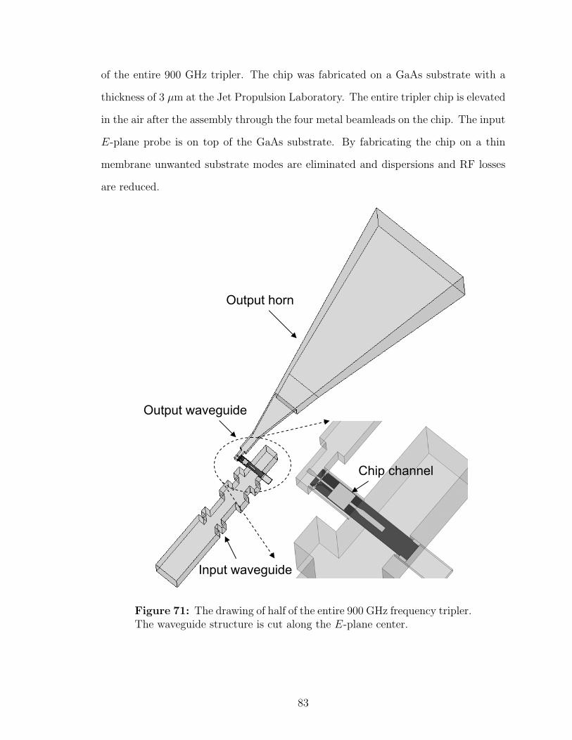
of the entire 900 GHz tripler. The chip was fabricated on a GaAs substrate with a
thickness of 3 µm at the Jet Propulsion Laboratory. The entire tripler chip is elevated
in the air after the assembly through the four metal beamleads on the chip. The input
E-plane probe is on top of the GaAs substrate. By fabricating the chip on a thin
membrane unwanted substrate modes are eliminated and dispersions and RF losses
are reduced.
Chip channel
Output horn
Output waveguide
Input waveguide
Figure 71: The drawing of half of the entire 900 GHz frequency tripler.The waveguide structure is cut along the E-plane center.
83

8.2.2 Waveguide Structure Design
Once the diode cell and size of the anodes has been optimized, the waveguide circuit
is designed around this to optimize performance. Therefore, the height of the chip
channel and the length of the backshorts are first optimized to maximize the coupling
at the center frequency. The input signals are coupled to the suspended microstrip line
that supports the propagation in the TEM mode. The transition that is optimized to
maximize the coupling at the center frequency doesn’t guarantee a wide bandwidth
because the impedance of a waveguide is frequency-dependent. Then, an eight-section
waveguide matching network is employed to extend the bandwidth without lowering
the output power. The same procedure is used to design the output coupling and
waveguide structure. The dimensions of the channel that runs between the input and
the output waveguides are set to cuto! the first TE mode of the suspended microstrip
line at the second harmonic, i.e. only a quasi-TEM mode is allowed to propagate
inside this channel at the input frequency and at the idler frequency; therefore the
second harmonic cannot propagate [122].The third harmonic propagates in the TEM
mode in the chip channel and is coupled to the output waveguide through the output
E-plane probe. During the circuit design special consideration is given to maintaining
equal input coupling between the two anodes, and this is necessary to avoid over
heating and diode burnout. The design topology, developed by Dr. Hui Wang and
shown in Figure 72, is adopted in the design of the 828-963-GHz Two-anode Frequency
Tripler [125].
8.2.3 The 900 GHz Membrane Chip
The purpose of the 900-GHz membrane chip is to provide a low-power source for
pumping Superconductor-Insulator-Superconductor (SIS) and Hot Electron Bolome-
ter (HEB) mixers. A unique feature of this chip is that almost all of the GaAs
84

Design Methodology of Frequency Multiplier
13
Schottky Diode Parameters
Schottky Diode Parameters
Optimization
(Non-linear analysis)
ADS
Passive EM Modeling
HFSS
(3D Structure )
Linear S-Parameter file
Rs, Cj0
Modification of 3D structure
Modification of anode size
Performance Prediction(maximum output power
and conversion efficiency)
Courtesy Dr. Hui WANG, RALFigure 72: The design methodology of the frequency tripler [125].
substrate is removed, leaving only a 3-µm-thick membrane to support the circuits in-
cluding diodes, probes, and impedance matching circuits. Monolithically integrated
metal beam leads provide easy handling and support for the chip, along with the
RF return for diodes. The entire chip can be simply dropped in the chip channel
without the use of solder or epoxy. The simplicity of the entire chip layout makes the
integration with waveguide circuits significantly easy and highly repeatable.
A simplified model of the Schottky diode is reported in [126], including a junction
capacitance Cj in parallel with a conductance and in series with a resistance Rs. The
series resistance consists of all impedance between the depletion region and the ohmic
contact, including the epilayer resistance, the dc series resistance of the substrate, and
the ohmic contact impedance [127]. The measured series resistance at dc is about 35
ohms per diode for this chip. The dc measurement of the series resistance, used as a
figure of merit of the diodes and reported in [122] and [127], is not enough to represent
the impedance at THz frequencies where skin e!ects and saturation e!ects cannot be
ignored. Based on previous RF measurements, the series resistance used in our ADS
85
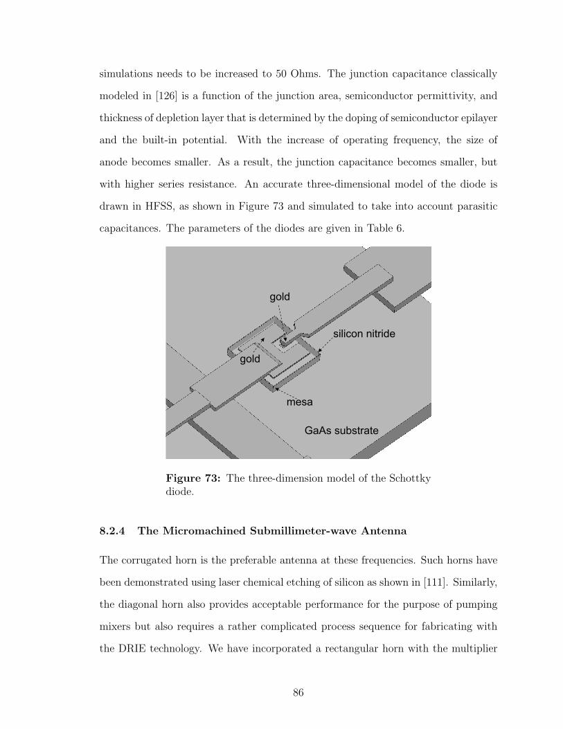
simulations needs to be increased to 50 Ohms. The junction capacitance classically
modeled in [126] is a function of the junction area, semiconductor permittivity, and
thickness of depletion layer that is determined by the doping of semiconductor epilayer
and the built-in potential. With the increase of operating frequency, the size of
anode becomes smaller. As a result, the junction capacitance becomes smaller, but
with higher series resistance. An accurate three-dimensional model of the diode is
drawn in HFSS, as shown in Figure 73 and simulated to take into account parasitic
capacitances. The parameters of the diodes are given in Table 6.
silicon nitride
mesa
gold
gold
GaAs substrate
Figure 73: The three-dimension model of the Schottkydiode.
8.2.4 The Micromachined Submillimeter-wave Antenna
The corrugated horn is the preferable antenna at these frequencies. Such horns have
been demonstrated using laser chemical etching of silicon as shown in [111]. Similarly,
the diagonal horn also provides acceptable performance for the purpose of pumping
mixers but also requires a rather complicated process sequence for fabricating with
the DRIE technology. We have incorporated a rectangular horn with the multiplier
86
Table 6: Physical and parameters and doing parameters of the JPL 900 GHz balancetripler.
Physical and electrical parameters
Anode width 0.4 µm
Anode length 1.4 µm
Epilayer doping 5!1017
GaAs thickness 3 µm
Cj 1.6 fF
Rs at DC 35 #
circuit. While this is not the optimum antenna structure it allows us to measure
the performance of the multiplier. This horn consists of a machined slope in the
fixture and a micromachined silicon part including the waveguide feed, transition and
aperture. Figure 74 (a) gives half of the horn split along the E-plane center. Figure 74
(b) depicts that the silicon part is on top of the fixture. Figure 74 (c) shows the silicon
part only.
The variable parameters in the design of horn are the flare angle *, the thickness
of the silicon t, the opening of the aperture a and b, and the length d. The horn,
following the output waveguide of the tripler, has a cross section of 110 µm by 230 µm.
The overall dimensions of the horn were initially chosen so that the horn would behave
like a rectangular horn. A full-wave simulation was performed using Ansoft’s HFSS.
The horn has the aperture of 2200 µm by 1676 µm. Table 7 shows the optimized
parameters of the horn. Figure 75 gives the far-field patterns of the horn, showing H-
plane peak copolarized sidelobes 17 dB down from the pattern peak and E-plane peak
copolarized sidelobes 10 dB down from the pattern peak. The 3-dB half-beamwidth
is 10!.
87
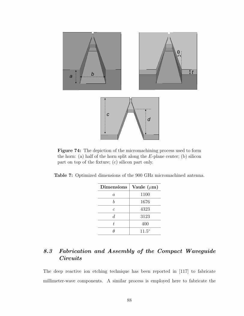
a b
!
t
cd
Figure 74: The depiction of the micromachining process used to formthe horn: (a) half of the horn split along the E-plane center; (b) siliconpart on top of the fixture; (c) silicon part only.
Table 7: Optimized dimensions of the 900 GHz micromachined antenna.
Dimensions Vaule (µm)
a 1100
b 1676
c 4323
d 3123
t 400
* 11.5!
8.3 Fabrication and Assembly of the Compact WaveguideCircuits
The deep reactive ion etching technique has been reported in [117] to fabricate
millimeter-wave components. A similar process is employed here to fabricate the
88

-60 -45 -30 -15 0 15 30 45 60-50
-40
-30
-20
-10
0
Am
plitu
de (d
B)
Angle (Degree)
E-plane Co-pol H-plane Co-pol
Figure 75: The simulated far-field patterns of the 900GHz micromachined horn.
waveguide structure for the 900 GHz tripler. The first step is to rinse low resistivity
silicon wafers (10-20 ohms-cm) and remove the organic residues. A layer of silicon
dioxide is deposited on both sides of the wafer using a plasma-enhanced chemical
vapor deposition process. Then, a photoresist layer is spun and patterned on the sili-
con dioxide layer. The exposed silicon oxide layer is etched away using a dry-etching
technique. The patterned silicon is etched using the deep reactive ion etching with
the BOSCH process. After that, the silicon substrate is flipped over and the process
is repeated starting from the spinning of the photoresist. The micromachined sam-
ples are released after the removal of the silicon dioxide. A 3-µm-thick metal layer of
Ti/Cu/Au is sputtered to form the metalized inner surfaces of waveguide structures.
The SEM images of the waveguide circuits and the dimensional sensitivity analysis
are given in Section IV in detail.
The fabricated silicon circuits are aligned through two alignment pins and mounted
on the fixture with the tripler chip in turn mounted on the Si pieces. The tolerance
of the fixture fabricated using direct machining is about 75 microns. A UG-387
89

waveguide flange forms at the input port of the fixture, as shown in Figure 76. The
tripler chip in the micromachined waveguide structure is shown in Figure 77. The
output of the fixture is the aperture of the horn antenna. The tolerance on the flange
and alignment pins will result in the reflection of input power. A useful analysis of
the waveguide flange misalignment can be found in [131] on a W -band waveguide.
According to this analysis, the misalignment in the height direction is worse than
that in the width direction for the same amount of misalignment over most of the
interested frequency range.
Silicon circuits
Input waveguide port
Figure 76: The fixture and the silicon circuits for mea-surement. A UG-387 waveguide flange forms at the inputwaveguide.
8.4 Measurement and Analysis
8.4.1 Measurement Setup
The measurement setup used for characterizing this 900 GHz tripler is shown in
Figure 78. A commercial synthesizer source in the W-band is amplified via W-band
power amplifiers. An attenuator, coupler and isolator are used before this signal is
used to drvie a broadband 300 GHz tripler [132]. The isolator is calibrated and the
90
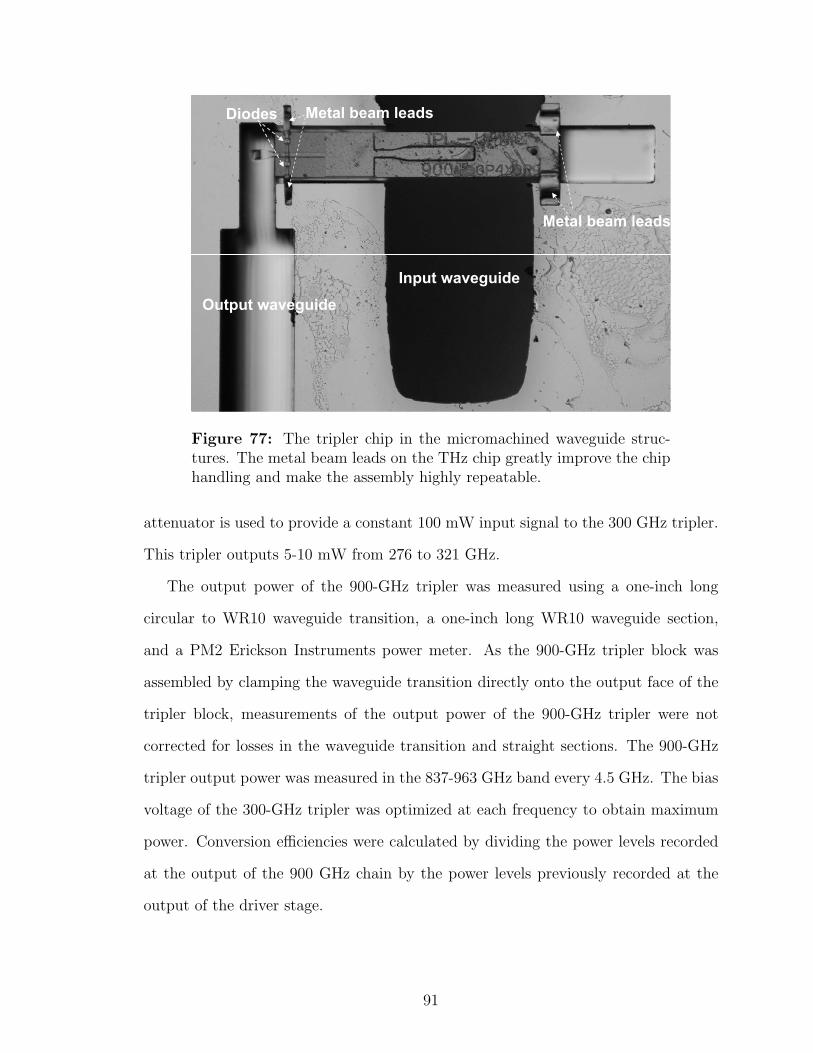
Input waveguideOutput waveguide
Diodes Metal beam leads
Metal beam leads
Figure 77: The tripler chip in the micromachined waveguide struc-tures. The metal beam leads on the THz chip greatly improve the chiphandling and make the assembly highly repeatable.
attenuator is used to provide a constant 100 mW input signal to the 300 GHz tripler.
This tripler outputs 5-10 mW from 276 to 321 GHz.
The output power of the 900-GHz tripler was measured using a one-inch long
circular to WR10 waveguide transition, a one-inch long WR10 waveguide section,
and a PM2 Erickson Instruments power meter. As the 900-GHz tripler block was
assembled by clamping the waveguide transition directly onto the output face of the
tripler block, measurements of the output power of the 900-GHz tripler were not
corrected for losses in the waveguide transition and straight sections. The 900-GHz
tripler output power was measured in the 837-963 GHz band every 4.5 GHz. The bias
voltage of the 300-GHz tripler was optimized at each frequency to obtain maximum
power. Conversion e"ciencies were calculated by dividing the power levels recorded
at the output of the 900 GHz chain by the power levels previously recorded at the
output of the driver stage.
91

Power Amp.92-107 GHz
Attn. Coupler
Power Meter
DUT
Transition
X3
RotaryAttenuator
Isolator
Tripler270-320 GHz
900-GHz Triplerin Silicon
WR-10PowerMeter
Circular to WR-10
PM2
Figure 78: The measurement setup. From the left to the right, themeasurement chain consists of a W -band power amplifier, a rotary vaneattenuator, a W-band coupler, an isolator, a WR10 waveguide, a JPLin-house 300-GHz tripler, the 900-GHz tripler, a circular to WR10 tran-sition, a WR-10 waveguide, and a PM2 power meter.
8.4.2 900 GHz Multiplier Frequency Response
The measured output power and the measured e"ciency of the 900 GHz tripler are
shown in Fiugre 79. At room temperature, the measured output power was 23.7 µW
to 85.3 µW from 828 GHz to 963 GHz and was above 60 µW from 877.5 GHz to
922.5 GHz. The input power generated by a 300 GHz tripler was 8.34 mW to 9.86
mW from 276 GHz to 321 GHz. In the estimated responses, the additional loss from
the surface roughness, reentrant angle, and silicon brim discussed below in detail is
considered as well as a total 1.5-dB de-embeded loss for the mismatching at input
flange and output, circular to WR-10 transition, and a 1-inch-long WR-10 waveguide.
However, no corrections have been made to the measured output power numbers.
92

820 840 860 880 900 920 940 960 9800
20
40
60
80
100
120
0.0
0.5
1.0
1.5
2.0
2.5
3.0 measured output power estimated output power
Out
put P
ower
(!W)
Frequency (GHz)
Effic
ienc
y (%
)
measured efficiency estimated efficiency
Figure 79: The estimate and measured output power and e"ciency at room temper-ature. No corrections have been made to the measured output power and e"ciencynumbers. At room temperature, the measured output power was 23.7 µW to 85.3µW from 828 GHz to 963 GHz.
8.4.3 Dimensional Sensitivity Analysis
Precision tolerances in the fabrication are vital to the THz frequency multipliers
because the operating wavelength is on the order of 300 µm at 900 GHz. Figure 80
shows the SEM images of the silicon waveguide structures, including output horn in
Figure 80(a), an input waveguide in Figure 80(b), a cross section of the waveguide
structure with the slope angle less than 2! in Figure 80(c) and the surface roughness
more than 1 µm in Figure 80(d).
Several tolerances in the fabrication are considered in this design. First, tolerances
exist in the mask layer used for dry etching. The mask layer, e.g. positive photoresist,
has a taper profile towards the sidewall, which means the thickness of the positive
photoresist is thinner on the edge than expected. The photoresist on the edge is
etched away first in a long etching process due to the limited selectivity, then the
photoresist-protected substrate is exposed and etched eventually. This phenomenon
leads to a wider opening of the etched features but can be compensated through
93
mask design. Second, tolerances from the deep reactive ion etching process normally
consist of the vertical striation and the reentrant angle. To reduce these tolerances,
the fabrication recipe is optimized by tuning many factors, including the pressure in
an etching chamber, the flow rate of gases, the time for etching and passivation, the
power of etching and passivation, and the exposed area of silicon. Our process has
been optimized to provide near 90! sidewalls.
The vertical striation worsens the surface roughness on the sidewall. In the THz
range, the current distributes itself near the surface of a transmission line due to the
skin e!ect. The surface roughness increases the total current path and leads to an
increase in conductor loss, which is usually computed by [130]:
+c
+c0= 1 +
2
%tan"1
$1.4
%%"
&2'
(10)
where %/" is the normalized rms roughness. The conductor loss +c0 can be
estimated using a full-wave simulator, e.g., HFSS. The skin depth of gold is about
120 nm at 300 GHz and the estimated rms roughness on sidewall is more than 1 µm,
as shown in Figure 80(d). Therefore, the increased conductor loss is about 0.02 dB
per wavelength at 300 GHz and 0.04 dB per wavelength at 900 GHz. As a result,
an additional 0.7 dB conductor loss comes from the surface roughness for the input
waveguide, output waveguide, and horn.
Di!erent from the vertical striation, the reentrant angle caused by the lack of
passivation on the sidewall in the etching cycle leads to an impedance mismatch
because of the deformation of the cross section. The e!ect of reentrant angle is
worse with the increase of etching depth. The fabrication recipe is first optimized to
minimize the reentrant angle. In addition, this tolerance is treated carefully in the
design and simulations to avoid degrading the performance substantially, especially
for the input waveguide structure that has the maximum depth.
Besides the vertical striation and reentrant angle, the bottom of a dry-etched
94

waveguide is hard to make flat, as shown in Figure 80(c) in this chapter and Figure 8
in [116]. This non-flat bottom results in a thin silicon brim left on the waveguide at the
end of the process when the silicon wafter is etched through. The silicon brim is only a
few microns thick and thus fragile enough to be broken by strong nitrogen flow, leaving
an irregular shape after the cleaning process. To further evaluate the tolerances of
the reentrant angle and the irregular shape, the input waveguide structure is scanned
and a 3-D model is built to represent these tolerances. The estimated additional loss
is about 0.65 dB using the simulation of Ansoft’s HFSS and Agilent’s ADS.
Irregular shape caused by silicon brim
Output waveguide
Chip channel
Input waveguide
Output horn Input waveguide
Cross section of waveguide sidewall
A corner of sidewall
Sidewall surface roughness
(a) (b)
(c) (d)
(e)
Figure 80: SEM images: (a) output horn; (b) input waveguide; (c) cross sectionof waveguide sidewall; (d) surface roughness on sidewall; (e) the input and outputbackshorts as well as the chip channel.
8.4.4 Power Sweep
The power sweep measurement was made at the frequency with the highest output
power. With the attenuator fully open and 150 mW driving the 300-GHz tripler,
a maximum power of 121.6 µW was recorded at 891 GHz. As the attenuator is
gradually closed, the output power of the 900-GHz tripler was recorded along with
the power measured at the W -band coupled port. The bias voltage of the 300-GHz
tripler was adjusted to get optimum output power at each point. To find the input
power going into the 900-GHz tripler, the last stage of the tripler was removed from
95

the measurement setup. The Erickson Instruments power meter and a WR-10 to WR-
3 waveguide transition was then attached to the 300-GHz tripler, and the power at
each point was measured by adjusting the attenuator until the W -band coupled port
power matches the previously recorded values, and the bias voltage of the 300 GHz
matches the previously set values. Conversion e"ciency was calculated in the same
way as was done in the frequency sweep. Figure 81 depicts the measured Pin-vs-Pout
at the frequency of 909 GHz for both output power and conversion e"ciency.
0 2 4 6 8 10 12 140
30
60
90
120
0.0
0.4
0.8
1.2
1.6
Effic
ienc
y (!)
Out
put P
ower
("W)
Input Power (mW)
output power efficiency
Figure 81: The measured output power and measurede"ciency v.s. input power at 909 GHz.
8.5 Conclusion
In the last two decades, the design of the THz multipliers and the fabrication of
diodes and chips had made extraordinary progress. In this work, silicon microma-
chined waveguide structures are successfully integrated, for the first time to the best
knowledge of the authors, seamlessly with THz chips at such high frequencies in
both the design and the measurement. This research result enables the silicon micro-
machining technique to build low-loss and low-cost THz signal sources. The tripler
96
provides state of the art performance, 23.7 µW to 85.3 µW from 828 GHz to 963
GHz and more than 60 µW from 877.5 GHz to 922.5 GHz, in a compact structure at
room temperature. Successful demonstration of this technology can now open up the
possibilities of using this approach for building multi-pixel heterodyne array receivers
for future applications.
97
CHAPTER IX
THE CONTRIBUTIONS AND PUBLICATIONS TO DATE
This thesis explored the design, simulation, fabrication, and characterization of micro-
machined millimeter-wave modules and signal source for submillimeter-wave output.
The primary contributions are summarized as the following items:
• The low-loss micromachined meander waveguide and filter
• The low-loss hybrid and power divider
• The novel low-loss CPW-to-waveguide transition and filter
• The novel high-Q 60 GHz cavity-based tunable resonator and filter
• The first 900 GHz frequency multiplier using silicon micromachined waveguides
This work in my Ph. D. study has led to the following publications:
9.1 Journal Publications
• Yuan Li, Pete L. Kirby, Olivier O!ranc, and John Papapolymerou, “Silicon
Micromachined W-band Hybrid Coupler and Power Divider Using DRIE Tech-
nique,” IEEE Microwave and Wireless Components Letters, Vol. 18, No. 1, pp
22 - 24, Jan. 2008.
• Yuan Li, Bo Pan, Cesar Lugo, Manos Tentzeris, John Papapolymerou, “Design
and Characterization of a W-Band Micromachined Cavity Filter Including a
Novel Integrated Transition From CPW Feeding Lines,” IEEE Transactions on
Microwave Theory and Techniques, Vol. 55, No. 12, pp. 2902-2910, December
2007.
98
• Bo Pan, Yuan Li, Manos M. Tentzeris and John Papapolymerou, “Surface Mi-
cromachining Polymer-Core-Conductor Approach for High Performance Millimeter-
Wave Air-Cavity Filter Integration,” IEEE Transactions on Microwave Theory
and Techniques, Vol. 56, No. 4, pp. 959-970, April 2008.
• Bo Pan, Yuan Li, Manos M. Tentzeris and John Papapolymerou, “A High-
Q Millimeter-Wave Air-lifted Cavity Resonator on Lossy Substrates,” IEEE
Microwave and Wireless Components Letters, Vol. 17, No. 8, pp 571 - 573,
Aug. 2007.
• Bo Pan, Yuan Li, George E. Ponchak, Manos M. Tentzeris and John Papapoly-
merou, “A Low-loss Substrate-Independent Approach for V-band Transceiver
Front-end Integration using Micromachining Technologies,” IEEE Transactions
on Microwave Theory and Technique, Vol. 56, No. 12, pp. 2779-2788, December
2008.
• Stanis Courreges, Yuan Li, Zhiyong Zhao, Kwang Choi, Andrew Hunt, Stephen
Horst, John D. Cressler, and John Papapolymerou “A Ka-Band Ferroelectric
Tunable Filter,” IEEE Microwave and Wireless Components Letters, Vol. 19,
No. 6, pp. 356-358, June 2009
• Stanis Courreges, Yuan Li, Z. Zhao, K. Choi, A. Hunt, J. Papapolymerou,
“A Quasi-Elliptic Ferroelectric Tunable Filter for X-Band Applications,” IEEE
Microwave and Wireless Components Letters, Vol. 19, No. 4, pp. 203-205,
April 2009.
• Stanis Courreges, Yuan Li, Z. Zhao, K. Choi, A. Hunt, J. Papapolymerou,
“Two-pole X-Band-Tunable Ferroelectric Filters with Tunable Center Frequency,
Fractional Bandwidth, and Return Loss,” IEEE Transactions on Microwave
Theory and Techniques, Vol. 57, No. 12, pp. 2872-2881, December 2009.
99

9.2 Conference Publications
• Yuan Li, Bo Pan, Manos M. Tentzeris, John Papapolymerou, “A Fully Micro-
machined W-Band Coplanar Waveguide to Rectangular Waveguide Transition,”
2007 IEEE International Microwave Symposium, pp. 1031 - 1034, Jun. 2007.
• Pete L. Kirby, Yuan Li, Qun Xiao, Je!eray Hesler, John Papapolymerou, “Sili-
con Micromachined Multiplier Utilizing Heterostructure Barrier Varactor Diode,”
2007 IEEE International Microwave Symposium, pp. 1141 - 1144, 3-8 Jun. 2007.
• Yuan Li, P. L. Kirby and J. Papapolymerou, “Silicon Micromachined W-Band
Bandpass Filter Using DRIE Technique, 2006 IEEE European Microwave Con-
ference, pp. 1271-1273, Manchester, Sep. 2006.
• Yuan Li, Pete L. Kirby and John Papapolymerou, “Silicon Micromachined W-
Band Folded and Straight Waveguides Using DRIE Technique, 2006 IEEE/MTT-
S International Microwave Symposium Digest, pp. 1915-1918, San Francisco,
CA, Jun. 2006.
• S. Courreges, Yuan Li, Z. Zhao, K. Choi, A. Hunt, J. Papapolymerou, “Ferro-
electric Tunable Bandpass Filters for Ka-Band Applications, 2008 IEEE Euro-
pean Microwave Conference Digest, pp. 56-58, 2008
• Bo Pan, Yuan Li, M.M.Tentzeris and J.Papapolymerou, “A Novel Low-loss
Integrated 60 GHz Cavity Filter with Source-Load Coupling using Surface Mi-
cromachining Technology”, 2008 IEEE-IMS Symposium, pp. 639-642, Atlanta,
June 2008.
• Pete L. Kirby, Yuan Li, Q. Xiao, J. Hesler, J. Papapolymerou, “Power Com-
bining Multiplier Using HBV Diodes at 260 GHz,” 2008 Asia-Pacific Microwave
Conference, pp. 1-4, Hong Kong, Dec. 2008.
100

• Yuan Li, J. Papapolymerou, “A Tunable High-Q Cavity Resonator through a
Current Probe and a Shunt Stub at 60 GHz,” 2009 IEEE European Microwave
Conference, pp. 197-200, Rome, Sep. 2009.
• D. Scarbrough, C. Goldsmith, J. Papapolymerou, and Yuan Li “X-Band RF
MEMS Tunable Two-Pole Waveguide Filter,” 2009 IEEE European Microwave
Conference, pp. 507-510, Sep. 2009.
101
REFERENCES
[1] http://www.itrs.net/
[2] B. Floyd, S. Reynolds, U. Pfei!er, T. Zwick, T. Beukema, and, B. Gaucher, “SiGebipolar transceiver circuits operating at 60 GHz” IEEE Journal of Solid-StateCircuits, vol. 40, no. 1, pp. 156-167, Jan. 2005.
[3] D. M. Kang, J. Y. Hong, J. Y. Shim, J. H. Lee, H. S. Yoon, and K. H. Lee, “A 77GHz automotive radar MMIC chip set fabricated by a 0.15 MHEMT technology,”in IEEE MTT-S Microwave Symp. Dig., Jun. 2005, pp. 21112114.
[4] A. Tessmann, S. Kudszus, T. Feltgen, M. Riessle, C. Sklarczyk, and W. H. Haydl,“A 94 GHz single-chip FMCW radar module for commercial sensor applications,”in IEEE MTT-S Microwave Symp. Dig., Jun. 2002, pp. 18511854.
[5] T. W. Crowe, W. L. Bishop, D. W. Porterfield, J. L. Hesler, and R. M. Weikle, II,“Opening the terahertz window with integrated diode currents,” IEEE J. Solid-State Circuits, vol. 40, no. 10, pp. 2104C2109, Oct. 2005.
[6] www.nasa.gov/vision/earth/lookingatearth/ozone five.html
[7] A. G. Engel Jr., L. P. B. Katehi, “Low-loss monolithic transmission lines forsub-millimeter and terahertz frequency applications,” IEEE Transactions on Mi-crowave Theory and Techniques, vol. 39, no. 11, pp.1847-1854, Nov. 1991.
[8] T. M. Weller, G. M. Rebeiz, and L P. B. Katehi,“Experimental Results on Mi-croshield Transmission Line Circuits,” IEEE MTT-S International MicrowaveSymposium, pp. 978-981, Jun. 1993.
[9] K. M. Strohm, F. J. Schmuckle, B. Schauwecker W. Heinrich, J. Luy , “SiliconMicromachined CPW Transmission Lines,” European Microwave Conference, pp.1-4, Oct. 2002.
[10] S. V. Robertson, L.P.B. Katehi, G.M. Rebeiz, “Micromachined W-band filters,IEEE Transactions on Microwave Theory and Techniques, vol. 44, No. 4, pp. 598606, Apr. 1996.
[11] B. Pan, Y. Yoon, Y. Zhao, J. Papapolymerou, M. M. Tentzeris and M. Allen, “ABroadband Surface-Micromachined 15-45 GHz Microstrip Coupler,” IEEE MTT-S International Microwave Symposium, pp.989-992, Jun. 2005.
[12] F. Bouchriha, K. Grenier, D. Dubuc, P. Pons, R. Plana, J. Gra!euil, ”CoplanarPassive Circuits on Surface Micromachined Silicon and Thick Polymer Layers forMillimeter-wave Applications,” European Microwave Conference, pp. 49-52, Oct.2003.
102
[13] G. E. Ponchak, I. K. Itotia, R. F. Drayton, “Propagation Characteristics ofFinite Ground Coplanar Waveguide on Si Substrates with Porous Si and PolyimideInterface Layers,” European Microwave Conference, pp. 45-48, Oct. 2003.
[14] G. Wang, A. Bacon, R. Abdolvand, F. Ayazi, J. Papapolymerou, and E.Tentzeris, “Finite Ground Coplanar Lines on CMOS Grade Silicon with a ThickEmbedded Silicon Oxide Layer Using Micromachining Techniques,” European Mi-crowave Conference, vol. 1, pp. 25-27, Oct. 2003.
[15] M. Rais-Zadeh and F. Ayazi, “Characterization of high-Q spiral inductors onthick insulator-on-silicon,” Journal of Micromechanics and Microengineering, vol.15, pp. 2105-2112, Sep. 2005.
[16] M. Raieszadeh, et al., “High-Q integrated inductors on trenched Si islands,”IEEE International Conference on Microelectromechanical Systems, pp. 199-202,Jan. 2005.
[17] M. J. Lancaster, Passive Microwave Device Applications of High-TemperatureSuperconductors, Cambridge University Press, Cambridge, 1997.
[18] Z.-Y. Shen, High-Temperature Superconducting Microwave Circuits, ArtechHouse, Norwood, MA 1994.
[19] Special Issue on Microwave and Communication Applications at Low Tempera-ture, IEEE Trans., MTT-48, July 2000, Part II.
[20] M. Zeisberger, M. Manzel, H. Bruchlos, M. Diegel, F. Thrum, M. Klinger, andA.Abramowicz, “TlBaCaCuOx thin films for microstrip filters,” IEEE Trans.,Applied Superconductivity, vol. 9, no. 6, pp.3897-3900, 1999.
[21] J. Papapolymerou, R.F. Drayton and L.P.B. Katehi, “Micromachined Patch An-tennas,” IEEE Transactions on Antennas and Propagation, vol. 46, no. 2, pp.275-283, Feb. 1998.
[22] S. V. Robertson, L. P. B. Katehi and G. M. Rebeiz, “W-band microshield lowpass filters,” IEEE MTT-S Dig., pp. 635-628, 1994.
[23] K. M. Strohm, F. J. Schmuckle, B. Schauwecker W. Heinrich, J. Luy , “SiliconMicromachined CPW Transmission Lines,” European Microwave Conference, pp.1-4, Oct. 2002.
[24] F. Bouchriha, K. Grenier, D. Dubuc, P. Pons, R. Plana, J. Gra!euil, “CoplanarPassive Circuits on Surface Micromachined Silicon and Thick Polymer Layers forMillimeter-wave Applications,” European Microwave Conference, pp. 49-52, Oct.2003.
[25] Z. Y. Zhang, K. Wu, “A Broadband Substrate Integrated Waveguide (SIW)Planar Balun,” IEEE Microwave and Wireless Components Letters, pp. 843-845,2007.
103

[26] T. Djerafi, K. Wu, “Super-Compact Substrate Integrated Waveguide CruciformDirectional Coupler,” IEEE Microwave and Wireless Components Letters, pp.757-759, 2007.
[27] J.-H. Lee, S. Pinel, J. Papapolymerou, J. Laskar, M. M. Tentzeris, “Low LossLTCC Cavity Filters Using System-on-Package Technology at 60 GHz,” IEEETransactions on Microwave Theory and Techniques, vol. 53, no. 12, pp. 3817-3828, Dec. 2005.
[28] A. El-Tager, J. Bray, and L. Roy, “High-Q LTCC Resonators For MillimeterWave Applications,” 2003 IEEE MTT-S Int. Microwave Digest, pp. 2257-2260,Jun. 2003.
[29] X. Gong, B. Liu, L. P. B. Katehi, and W. J. Chappell, “Laser-based polymerstereolithography of vertically integrated narrow bandpass filters operating in Kband,” IEEE MTT-S Int. Microwave Symp. Dig., pp. 425-428, Jun. 2004.
[30] X. Gong, A. Margomenos, L. Bosui, S. Hajela, L. P. B. Katehi, W. J. Chap-pell, “Precision fabrication techniques and analysis on high-Q evanescent-moderesonators and filters of di!erent geometries,” IEEE Transactions on MicrowaveTheory and Techniques, vol. 52, no. 11, pp. 2557-2566, Nov. 2004.
[31] S. P. Pancheo, Linda P. B. Katehi and T. -C. Nguyen, “Design of Low ActuationVoltage RF MEMS Switch,” IEEE MTT-S International Symposium, pp.165-168,vol.1, 2000.
[32] G. Wang, D.Thompson, M.M.Tentzeris and J.Papapolymerou, “Low Cost RFMEMS Switches Using LCP Substrate”, Procs. of the 2004 European MicrowaveSymposium, pp.1441-1444, Oct. 2004.
[33] B. Pan, Y. Yoon, P. Kirby, J. Papapolymerou, M. M. Tentzeris, and M. G.Allen, “A W-band Surface Micromachined Monopole for Low-cost Wireless Com-munication Systems,” Proc.of IEEE International Microwave Symposium 2004,pp.1935-1938, Jun. 2004.
[34] Y. K. Yoon, Jin-Woo Park, Mark G. Allen, ”Polymer-core conductor approachesfor RF MEMS, Journal of Microelectromechanical Systems, vol. 14, no. 5, Oct.2005.
[35] Y. K. Yoon, Jung-Hwan Park, M. G. Allen, “Multidirectional UV lithographyfor complex 3-D MEMS structures,” Journal of Microelectromechanical Systems,vol. 15, no. 5, pp. 1121-1130, Oct. 2006.
[36] B. Pan, Y. Li, M. M. Tentzeris and J. Papapolymerou, “Surface MicromachiningPolymer-Core-Conductor Approach for High Performance Millimeter-Wave Air-Cavity Filter Integration,” IEEE Transactions on Microwave Theory and Tech-niques, vol. 56, no. 4, pp. 959-970, April 2008.
104
[37] B. Pan, Y. Li, M. M. Tentzeris and J. Papapolymerou, “A Low-loss Substrate-Independent Approach for 60 GHz Transceiver Front-end Integration using Mi-cromachining Technologies,” IEEE Transactions on Microwave Theory and Tech-niques, vol. 56, no. 12, pp. 2779-2788, December 2008.
[38] G.T. Kovacs, Micromachined Transducers Sourcebook, McGrawHill, 1998.
[39] http://soral.as.arizona.edu/micromachining.html
[40] Y. Lee, J. P. Becker, J. R. East, and L. P. B. Katehi, “A micromachined finitecoplanar line-to-silicon micromachined waveguide transition for millimeter andsubmillimeter wave applications,” IEEE MTT-S Int. Microwave Symp. Dig., pp.1871-1874, 2002.
[41] ASE processing fundamentals, seminar from STS Technology System, 2005
[42] Y. Li, P. L. Kirby and J. Papapolymerou, “Silicon Micromachined W-BandFolded and Straight Waveguides Using DRIE Technique,” IEEE MTT-S Inter-national Microwave Symposium Digest, pp. 1915-1918, Jun. 2006.
[43] N. Sahri, T. Nagatsuma, K. Machida, H. Ishii, H Kyuragi, “Characterizationof Micromachined Coplanar Waveguides on Silicon up to 300 GHz,” EuropeanMicrowave Conference, vol. 1, pp. 254 - 257, Oct. 1999.
[44] Available: http://aerowave.net/InfoFiles/WaveguideTable.pdf
[45] V. Subramanian, Z. Zhang, D. Gruner, F. Korndoerfer, G. Boeck, “Analysisand characterization of microstrip structures up to 90 GHz in SiGe BiCMOS,”European Microwave Conference, pp. 512 - 515, 2007.
[46] V. Subramanian, Z. Zhang, D. Gruner, F. Korndoerfer, G. Boeck, “Analysisand characterization of microstrip structures up to 90 GHz in SiGe BiCMOS,”European Microwave Conference, pp. 512 - 515, 2007.
[47] Y. Li, Pete L. Kirby and J. Papapolymerou, “Silicon Micromachined W-BandBandpass Filter Using DRIE Technique,” IEEE European Microwave ConferenceDigest, pp. 1271-1273, Sep. 2006.
[48] E. Rampnoux, P. Blondy, D. Cros, S. Verdeyme, M. Trier, C. Zanchi, “Microma-chined Ka and W - Band Filters For Space Radiometric Applications,” EuropeanMicrowave Conference, pp. 1-4, 2001.
[49] G. Matthaei, L. Yound and E. M. T. Jones, Microwave Filters, Impedance-Matching Networks, and Coupling Structure, MA, Artech House, 1980.
[50] C. D. Nantista and S.G. Tantawi, “A compact, planar, eight-port waveguidepower divider/combine: the cross potent superhybrid,” IEEE Microwave andWireless Comp. Lett., vol. 10, no. 12, pp. 520-522, Dec. 2000.
105
[51] S. V. Robertson, A.R. Brown, L.P.B. Katehi, , G.M. Rebeiz, “A 10-60-GHzmicromachined directional coupler, IEEE Transactions on Microwave Theory andTechniques, vol. 46, no. 11, Part 2, pp. 1845-1849, 1998.
[52] Y. Li, B. Pan, M. M. Tentzeris, J. Papapolymerou, “A Fully Micromachined W-Band Coplanar Waveguide to Rectangular Waveguide Transition,” IEEE MTT-SInternational Microwave Symposium, pp. 1031-1034, Jun. 2007.
[53] A. J. Simmons, “Phase shift by periodic loading of waveguide and its applicationto broad-band circular polarization,” IEEE Trans. Microw. Theory Tech., vol. 3,no. 6, pp. 18-21, Dec. 1955.
[54] N. Marcuvitz, Waveguide Handbook, Radiation Laboratory, vol. 10, 1st Edition,pp. 335, 1951.
[55] G. E. Ponchak and R. N. Simons, “A New Rectangular Waveguide to Coplanar-Waveguide Transition,” IEEE MTT-S Int. Microwave Symp. Dig., Dallas, TX,Vol. 1, pp. 491-492, May 8-10, 1990.
[56] E. M. Godshalk, “A V-Band Wafer Probe Using Ridge-Trough Waveguide,”IEEE Trans. Microwave Theory Tech., Vol. 39, No. 12, pp. 2218-2228, Dec. 1991.
[57] R. N. Simons, “New Channelized Coplanar Waveguide to Rectangular WaveguidePost and Slot Couplers,” Electron. Letter, Vol. 27, No. 10, pp. 856-857, May 1991.
[58] R. N. Simons, Coplanar waveguide circuits, components and systems. Wiley-Interscience, USA, 2001
[59] D. Deslandes and K. Wu, “Integrated microstrip and rectangular waveguide inplanar form,” IEEE Microw. Wireless Compon. Lett., vol. 11, no. 2, pp. 68-70,Feb. 2001.
[60] N. Jain and N. Kinayman, “A novel microstrip mode to waveguide mode trans-former and its applications,” in IEEE MTT-S Int. Microwave Symp. Dig., May2001, pp. 623-626.
[61] D. Deslandes and K. Wu, “Analysis and design of current probe transition fromgrounded coplanar to substrate integrated rectangular waveguides,” IEEE Trans.Microw. Theory Tech., vol. 53, no. 8, pp. 2487-2494, Aug. 2005.
[62] D. Deslandes and K. Wu, “Integrated transition of coplanar to rectangular waveg-uides,” in IEEE MTT-S Int. Microwave Symp. Dig., May 2001, pp. 619-622.
[63] Y. Huang, K.-L. Wu, and M. Ehlert, “An integrated LTCC laminated waveguide-to-microstrip line T-junction,” IEEE Microw. Wireless Compon. Lett., vol. 13, no.8, pp. 338-339, Aug. 2003.
[64] J. H. Lee, N.Kidera, S. Pinel, J. Papapolymerou, J.Laskar, and M.M.Tenzeris,“Comparative Study of Feeding Techniques for 3D Cavity Resonators,” IEEETransactions on Advanced Packaging, Vol.30, No.1, pp.115-123, Feb. 2007.
106
[65] [78] Y. Huang and K.-L. Wu, “A broad-band LTCC integrated transition of lam-inated waveguide to air-filled waveguide for millimeter-wave applications,” IEEETrans. Microw. Theory Tech., vol. 51, no. 5, pp. 1613-1617, May 2003.
[66] Y. Lee, J. P. Becker, J. R. East, and L. P. B. Katehi, “A micromachined finitecoplanar line-to-silicon micromachined waveguide transition for millimeter andsubmillimeter wave applications,” in IEEE MTT-S Int. Microwave Symp. Dig.,2002, pp. 1871-1874.
[67] Y. Lee, J. P. Becker, J. R. East, and L. P. B. Katehi, “Fully micromachined finite-ground coplanar line-to-waveguide transitions for W-band applications,” IEEETrans. Microw. Theory Tech., vol. 52, no. 3, pp. 1001-1007, Mar. 2004
[68] R. E. Collin, Foundation for Microwave Engineering, McGraw-Hill, 2nd edition,USA, pp. 281, 1992.
[69] I. A. Eshrah, A. A. Kishk, A. B. Yakovlev, and A. W. Glisson, “Equivalentcircuit model for awaveguide probe with application to DRA excitation, IEEETrans. Antennas Propag., vol. 54, no. 5, pp. 1433-1441, May 2006.
[70] W. W. Mumford, “The optimum piston position for wide-band coaxialto-waveguide transducers, Proc. IRE, vol. 41, pp. 256-261, Feb. 1953.
[71] J. A. Ruiz-Cruz, M. El Sabbagh, K. A. Zaki, and J. M. Rebollar, “Fullwave designof canonical ridge waveguide filters,” in IEEE MTT-S Int. Microwave Symp. Dig.,2004, pp. 603-606.
[72] J. Gipprich, D. Stevens, M. Hageman, A. Piloto, K. A. Zaki, and Y. Rong,“Embedded waveguide filters for microwave and wireless applications using cofiredceramic technologies,” in Proc. Int. Microelectronics Symp., San Diego, CA, 1998,pp. 23-26.
[73] Y. Rong, K. A. Zaki, M. Hageman, D. Stevens, and J. Gipprich, “Lowtempera-ture cofired ceramic (LTCC) ridge waveguide bandpass chip filters,” IEEE Trans.Microw. Theory Tech., vol. 47, no. 2, pp. 2317-2324, Feb. 1999.
[74] M. El Sabbagh, H.-T. Hsu, and K. A. Zaki, “Full-wave optimization of striplinetapped-in ridge waveguide bandpass filters,” in IEEE MTT-S Int. MicrowaveSymp. Dig., pp. 1805-1808, Jun. 2002.
[75] S. Amari, “Sensitivity of coupled resonator filters,” IEEE Circuits Syst. II, vol.47, pp. 1017-1022, Oct. 2000.
[76] Y. Li, B. Pan, C. Lugo, M. Tentzeris, J. Papapolymerou, “Design and Charac-terization of a W-Band Micromachined Cavity Filter Including a Novel IntegratedTransition From CPW Feeding Lines,” IEEE Transactions on Microwave Theoryand Techniques, Vol. 55, No. 12, pp. 2902-2910, December 2007.
107
[77] K. M. Strohm, F. J. Schmuckle, O. Yaglioglu, J-F. Luy, and W. Heinrich, “3DSilicon Micromachined RF resonator,” IEEE MTT-S Digest, pp. 1801-1804, 2003.
[78] J. P. Becker and L. P. B. Katehi, “Toward a novel planar circuit compatible sili-con micromachined waveguide,” IEEE Electrical Performance of Electronic Pack-aging, pp. 221-224, 1999.
[79] X. Gong, A. Margomenos, B. Liu, S. Hajela, L. P. B. Katehi, W. J. Chap-pell, “Precision fabrication techniques and analysis on high-Q evanescent-moderesonators and filters of di!erent geometries,” IEEE Transactions on MicrowaveTheory and Techniques vol. 52, no. 11, pp. 2557-2566 2004.
[80] J.-H. Lee, N. Kidera, S. Pinel, J. Papapolymerou, J. Laskar, and M. M. Tentzeris,“Comparative Study of Feeding Techniques for 3D Cavity Resonators,” IEEETransactions on Advanced Packaging, vol. 30, no. 1, pp.115-123, Feb. 2007.
[81] W. Steyn, P. Meyer, “A shorted waveguide-stub coupling mechanism for narrow-band multimode coupled resonator filters,” IEEE Transactions on Microwave The-ory and Techniques, vol. 52, no.6, pp.1622-1625, Jun. 2004.
[82] H. Joshi, H. Sigmarsson, H. Peroulis, W. J. Chappell, “Highly Loaded EvanescentCavities for Widely Tunable High-Q Filters,” IEEE MTT-S Digest, pp.2133-2136,Jun. 2007.
[83] Y. Zhao, S. Kim, Y. Li, B. Pan, X. Wu, E. M. Tentzeris, J. Papapolymerou,Mark G. Allen, “A micromachined airflow sensor based on RF evanescent-modecavity tesonator,” IEEE MTT-S Digest, pp. 1199-1203, 2008.
[84] H. Kannan and T. Weller, “Multi-Finger RF MEMS Variable Capacitors for RFApplications,” European Microwave Conference, pp.717-720, 2004.
[85] L. Dussopt, G.M. Rebeiz, “Intermodulation distortion and power handling in RFMEMS switches, varactors, and tunable filters,” IEEE Transactions on MicrowaveTheory and Techniques, vol. 51, no. 4, pp. 1247-1256, Apr. 2003.
[86] C. L. Goldsmith, D. I. Forehand, Z. Peng, J. C. M. Hwang, and J. L. Ebel,“High-cycle life testing of RF-MEMS switches,” IEEE MTT-S Digest, pp. 1805-1808, Jun. 2007.
[87] J.-S. Fu, X. A. Zhu, J. D. Phillips, A. Mortazawi, “Improving Linearity ofFerroelectric-Based Microwave Tunable Circuits,” IEEE Transactions on Mi-crowave Theory and Techniques, vol. 55, no. 2, pp. 354-360, Feb. 2007.
[88] I. Mehdi, P. Siegel, “THz semiconductor-based front-end receiver technology forspace applications,” IEEE Radio and Wireless Conf., Atlanta, Georgia, Sep. 2004,pp. 127-130.
[89] G. Convert, T. Yeou, and B. Pasty, “Millimeter-wave O-carcinotron,” in Proc.Symp. Millimeter Waves, vol. IX, NY, Mar. 31-Apr. 2 1959, pp. 313-339.
108

[90] G. Kantorowicz and P. Palluel, “Backward Wave Oscillators,” Infrared and Mil-limeter Waves, vol. 1, Academic Press, Ch. 4, 1979.
[91] Q. Xiao, J. L. Hesler, T. W. Crowe, B. S. Deaver, and R. M. Weikle, “A 270-GHzTuner-Less Heterostructure Barrier Varactor Frequency Tripler,” IEEE Microw.Compon. Lett., vol. 17, no. 4, pp. 241-243, Apr. 2007.
[92] J. Vukusic, B. Alderman, T. A. Emadi, M. Sadeghi, A. O. Olsen, T. Bryllert, J.Stake, “HBV tripler with 21% e"ciency at 102 GHz,” Electronics Lett., vol. 42,no. 6, pp. 355-356, Mar. 2006.
[93] T. Bryllert, A. Olsen, J. Vukusic, T. A. Emadi, M. Ingvarson, J. Stake, D. Lip-pens, “11% e"ciency 100 GHz InP-based heterostructure barrier varactor quin-tupler,” Electronics Lett., vol. 41, no. 3, pp. 131-132, Feb. 2005.
[94] L. Chusseau, J. F. Lampin, S. Bollaert, L. Duvillaret, J. Mangeney, “THz activedevices and applications: a survey of recent researches,” European MicrowaveConf., Paris, Oct. 2005, pp. 4-6.
[95] W. Hafez and M. Feng, “Experomental demonstration of pseudomorphic hetero-junction bipolar transistors with cuto! frequencies above 600 GHz,” Appl. Phys.Lett., vol. 86, pp. 152101-3, 2005.
[96] P. H. Siegel, “THz Technology,” IEEE Trans. Microw. Theory Tech. 50th An-niversary Issue, vol. 50, no. 3, pp. 910-928, Mar. 2002.
[97] Imran Mehdi, E. Schlecht, G. Chattopadhyay and P.H. Siegel, “THz Local Os-cillator Sources: Performance and Capabilities,” Astronomical Telescopes and In-strumentation, Waikoloa, Hawaii, Aug. 2002.
[98] J. Ward, E. Schlecht, G. Chattopadhyay, H. Javadi, J. Gill, I. Mehdi, A.Maestrini, and C. Tripon Canseliet, “Local Oscillators from 1.4 to 1.9 THz, Proc.of the 16th Int. Symp. on Space Terahertz Technology, Gteborg, Sweden, May2005, pp. 374-377.
[99] C. M. Mann, “Fabrication Technologies for Terahertz Waveguide”, IEEE 6th Int.Conf. on Terahertz Electronics, Leeds, Sep. 1998, pp. 46-49.
[100] X. Melique, A. Maestrini, R. Farre, P. Mounaix, M. Favreau, O. Vanbe- sien,J. Goutoule, F. Mollot, G. Beaudin, T. Nahri, and D. Lippens, “Fabrication andperformance of InP-based heterostructure barrier var- actors in 250-GHz waveg-uide tripler, IEEE Trans. Microw. Theory Tech., vol. 48, no. 6, pp. 1000-1006,Jun. 2000.
[101] A. Maestrini, J. S. Ward, C. Tripon-Canseliet, J. J. Gill, C. Lee, H. Javadi,G. Chattopadhyay, and I. Mehdi, “In-Phase Power-Combined Frequency Triplersat 300 GHz,” IEEE Microw. Wireless Compon. Lett., vol. 18, no. 3, pp. 218-220,Mar 2008.
109

[102] P. L. Kirby, Yuan Li, Q. Xiao, J. Hesler, J. Papapolymerou, “Power CombiningMultiplier Using HBV Diodes at 260 GHz, Asia-Pacific Microw. Conf., HongKong, Dec. 2008, pp. 1-4.
[103] V. M. Lubecke, K. Mizuno, and G. M. Rebeiz, “Micromachining for TerahertzApplications,” IEEE Trans. Microw. Theory Tech., vol 46, no. 11, pp 1821-1831,Nov. 1998.
[104] P. H. Siegel, R. P. Smith, S. Martin, M. Gaidans “2.5-THz GaAs MonolithicMembrane-Diode Mixer,” IEEE Trans. Microw. Theory Tech., vol. 47, no. 5, pp.596-604, May 1999.
[105] J. L. Hesler, K. Hui, R.K. Dahlstrom, R.M. Weikle, T.W. Crowe, C.M. Mann,H.B. Wallace, “Analysis of an Octagonal Micromachined Horn Antenna forSubmillimeter-Wave Applications,” IEEE Trans. on Antennas and Propag., vol.49, no. 6, pp. 997-1001, Jun. 2001.
[106] J. Digby, C. McIntosh, G. Parkhurst, B. Towlson, S. Hadjiloucas, J. Bowen, J.Chamberlain, R. Pollard, R. Miles, D. Steenson, L. Karatzas, N. Cronin, and S.Davies, “Fabrication and characterization of micro- machined rectangular waveg-uide components for use at millimeter- wave and terahertz frequencies,” IEEETrans. Microw. Theory Tech., vol. 48, no. 8, pp. 1293-1302, Aug. 2000.
[107] X. Gong, B. Liu, L. P. B. Katehi, and W. J. Chappell, ”Laser-based polymerstereolithography of vertically integrated narrow bandpass filters operating in Kband,” IEEE MTT-S Int. Microwave Symp. Dig., pp. 425-428, Jun. 2004.
[108] X. Gong, A. Margomenos, L. Bosui, S. Hajela, L. P. B. Katehi, W. J. Chappell,”Precision fabrication techniques and analysis on high-Q evanescent-mode res-onators and filters of di!erent geometries,” IEEE Trans. Microw. Theory Tech.,vol. 52, no. 11, pp. 2557-2566, Nov. 2004.
[109] L. Ives, C. Kory, M. Read, J. Neilson, “Development of terahertz backward waveoscillators,” Conf. Dig. of the 28th Infared and Millimeter Waves, pp. 249-250,Otsu, Japan, 2003.
[110] C. K. Walker, G. Narayanan, A. Hungerford, T. Bloomstein, S. Palmacci, M.Stern, J. Curtin, J., “Laser Micromachining of Silicon: A New Technique forFabricating TeraHertz Imaging Arrays,” Proc. SPIE, Astronomical Telescopes andInstrumentation, Kona, Hawaii, 1998, pp. 45-52.
[111] Available: http://soral.as.arizona.edu/micromachining.html.
[112] W. R. McGrath, C. Walker, M. Yap, Y. -C. Tai, “Silicon micromachined waveg-uides for millimeter-wave and submillimeter-wave frequencies,” IEEE Microw.Guid. Wave Lett., vol. 3, no. 3, pp. 61-63, Mar. 1993.
[113] S. Robertson, L. Katehi, and G. Rebeiz, “Micromachined W-band filters,” IEEETrans. Microw. Theory Tech., vol. 44, no. 4, pp. 598-606, Apr. 1996.
110

[114] J. L. Hesler, K. Hui, and T. Crowe, “Analysis of an octagonal micromachinedhorn antenna for submillimeter-wave applications,” IEEE Trans. on Antennas andPropag., vol. 49, pp. 997-1001, Jun. 2001.
[115] K. Hui, J. L. Hesler, D. S. Kurtz, W. L. Bishop, and T. W. Crowe, “A micro-machined 585 GHz Schottky mixer,” IEEE Micro. and Guid. Wave Lett., vol. 10,pp. 374-376, Sep. 2000.
[116] Y. Lee, J. P. Becker, J. R. East, and L. P. B. Katehi, “Fully Microma-chined Finite-Ground Coplanar Line-to-Waveguide Transistors for W-Band Ap-plications,” IEEE Trans. Microw. Theory and Tech., vol. 52, no. 3, pp. 1001-1007,Mar. 2004.
[117] Y. Li, P. L. Kirby, O. O!ranc, and J. Papapolymerou “Silicon MicromachinedW-band Hybrid Coupler and Power Divider Using DRIE Technique,” IEEE Mi-crow. Wireless Compon. Lett., vol. 18, no. 1, pp 22-24, Jan. 2008.
[118] P. L. Kirby, D. Pukala, H. Manohara, I. Mehdi and J. Papapolymerou, “Char-acterization of Micromachined Silicon Rectangular Waveguide at 400 GHz,” IEEEMicrow. Wireless Compon. Lett., vol. 18, no. 1. pp. 366-368, Jun. 2006.
[119] G. Chattopadhyay, J. S. Ward, H. Manohara, R. Toda, “Deep Reactive IonEtching based silicon micromachined components at terahertz frequencies forspace applications,” Infrared, Millimeter and Terahertz Waves, pp.1-2, Sep. 2008.
[120] P. L. Kirby, Y. Li, Q. Xiao, J. Hesler, J. Papapolymerou, ”Silicon Microma-chined Multiplier Utilizing Heterostructure Barrier Varactor Diode,” IEEE MTT-S Int. Microwave Symp. Dig., Hawaii, Jun. 2007, pp. 1141-1144.
[121] J. Schur, S. Biber, O. Cojocari, B. Mottet, L. P. Schmidt, and H. L. Hart-nagel, “600 GHz heterodyne mixer in waveguide technology using a GaAs Schot-tky diode,” in Int. Sym. on Space Terahertz Tech., Goteborg, Schweden, May2005, pp. 469-470.
[122] A. Maestrini, J. Ward, J. Gill, H. Javadi, E. Schlecht, C. Tripon- Canseliet,G. Chattopadhyay and I. Mehdi, “A 540-640 GHz High E"ciency Four AnodeFrequency Tripler,” IEEE Trans. Microw. Theory Tech., vol. 53, no. 9, pp. 2835-2843, Sep. 2005.
[123] N. R. Erickson, R. P. Smith, S. C. Martin, B. Nakamura, and I. Mehdi, “Highefciency MMIC frequency triplers for millimeter and submil- limeter wavelengths,”in IEEE MTT-S Int. Microwave Symp. Dig., Boston, MA, Jun. 2000, pp. 1003-1006.
[124] R. F. Bradley, “The application of planar monolithic technology to Schottkyvaractor millimeter-wave frequency multipliers,” Ph.D. dissertation, Sch. Eng.Appl. Science, Univ. of Virginia, Charlottesville, May 1992.
111

[125] A. Maestrini, “Wideband THz frequency multiplier chains for local oscillators,”in THz workshop, European Microwave Week, 2009.
[126] G. Massobrio and P. Antognetti, Semiconductor Device Modeling with SPICE,2nd ed. New York: McGraw-Hill, 1993.
[127] T. W. Crowe, R. J. Mattauch, H. P. Roser, W. L. Bishop, W. C. B. Peatman,and X. Liu, “GaAs Schottky diodes for THz mixing applica- tions,” Proc. IEEE,vol. 80, no. 11, pp. 1827-1841, Nov. 1992.
[128] N. R. Erickson, “Diode frequency multipliers for terahertz local-os- cillator ap-plications,” in Proc. SPIE, vol. 3357, Advanced Technology MMW, Radio, andTerahertz Telescopes, Mar. 1998, pp. 75-84.
[129] J. F. Johansson, and N. D. Whyborn, “The Diagonal Horn as a SubmillimeterWave Antenna.” IEEE Trans. on Microw. Theory and Tech., vol 40, no. 5, pp.795-800, May 1992.
[130] M. V. Lukic, D. S. Filipovic, “Modeling of 3-D surface roughness e!ects withapplication to -coaxial lines,” IEEE Trans. on Microw. Theory and Tech., vol. 55,no. 3, pp. 518-525, Mar. 2007.
[131] A. R. Kerr, E. Wollack, and N. Horner, “Waveguide flanges for ALMA instru-ments,” ALMA memo 278, Nov. 1999.
[132] A. Maestrini, C. Tripon-Canseliet, J. S. Ward, J. J. Gill, and I. Mehdi, “A Highe"ciency Multiple-Anode 260-340 GHz Frequency Tripler,” 17th Int. Conf. onSpace Terahertz Tech., Paris, May 2006, pp. 2-5.
112