Review of 20 Years of Research on Microwave and Millimeter-wave Lenses at “Instituto de...
20
Review of 20 Years of Research on Microwave and Millimeter-wave Lenses at “Instituto de Telecomunicações” Carlos A. Fernandes 1 , Jorge R. Costa 1,2 , Eduardo B. Lima 1 , and Mário G. Silveirinha 3 1 Instituto de Telecomunicações, Instituto Superior Técnico, University of Lisbon, 1049-001 Lisbon, Portugal E-mails: [email protected]; [email protected] 2 Instituto Universitário de Lisboa (ISCTE-IUL), 1649-026 Lisbon, Portugal E-mail: [email protected] 3 Department of Electrical Engineering, Instituto de Telecomunicações, University of Coimbra, 3030 Coimbra, Portugal Abstract Starting from a challenge in the early 1990s to develop a highly shaped beam dielectric lens antenna for a pilot 150 Mb/s cellular mobile broadband system operating in the 60-GHz band, several new developments have been ac- complished over more than 20 years at Instituto de Telecomunicações [1] in the areas of millimeter-wave shaped di- electric lens antennas and planar metamaterial lenses. We review here a few representative examples with numerical and experimental results, covering applications in mobile broadband communications, radiometry, satellite communications, multigigabit short-range communications, and sublambda near-field target detection. Keywords: Beam-steering antennas; geometrical optics (GO) and physical optics (PO); lens antennas; metamaterial lenses; millimeter- and submillimeter-wave antennas; reflector antenna feeds; scanning antennas; shaped beam an- tennas; wireless communications 1. Introduction D ielectric lenses were proposed as an alternative to re- flector antennas as early as the 1940s [2]. Unlike re- flector antennas, the beam shaping effect in lenses is achieved by placing the feed behind the lens; this eliminates the aperture blocking by the feed and the related adverse ef- fects. Subsequent systematic studies of lens antennas showed its design flexibility to meet demanding radiation pattern specifications [3], [4]. Early lens designs were intended for microwave applications; at those wavelengths, dielectric lenses were bulky and heavy even when zoned, and thus, they were suitable only for selected applications. It was not until the 1980s and 1990s that dielectric lenses have gained new interest, pushed by new challenges in millimeter- and submillimeter-wave applications [5]–[8]. In 1992, a research team from the “Instituto de Teleco- municações” (IT) [1] participated in the European project Mobile Broadband Systems (MBS) [9]. The project goal was to demonstrate the feasibility of a cellular mobile broadband system offering a high bit rate of 150 Mb/s per user, with mobile speeds up to 100 km/h, operating in the 60-GHz oxy- gen absorption band. One of IT tasks was to develop a new antenna concept to cope with unusual specifications: due to the limited power available from solid-state devices at these wavelengths and the need to maintain multipath propagation at a controlled level, the base station antenna was required to produce constant flux illumination over the whole cell with a sharp coverage drop near the cell edges. Therefore, the an- tenna not only needed to produce a csc 2 shape radiation pattern within the cell, but cumulatively the coverage foot- print needed to conform to the prescribed cell geometry, typ- ically a very elongated rectangle like a long section of a street. Highly shaped lenses with an embedded feed emerged as the preferred approach to obtain an effective relatively Digital Object Identifier 10.1109/MAP.2015.2397156 Date of publication: 5 March 2015 IEEE Antennas and Propagation Magazine, Vol. 57, No. 1, February 2015 1045-9243/15/$26.00 © 2015 IEEE 249
Transcript of Review of 20 Years of Research on Microwave and Millimeter-wave Lenses at “Instituto de...
Review of 20 Years of Research onMicrowave and Millimeter-wave Lensesat “Instituto de Telecomunicações”
Carlos A. Fernandes1, Jorge R. Costa1,2, Eduardo B. Lima1, and Mário G. Silveirinha3
1Instituto de Telecomunicações, Instituto Superior Técnico,University of Lisbon, 1049-001 Lisbon, Portugal
E-mails: [email protected]; [email protected]
2Instituto Universitário de Lisboa (ISCTE-IUL), 1649-026 Lisbon, PortugalE-mail: [email protected]
3Department of Electrical Engineering, Instituto de Telecomunicações,University of Coimbra, 3030 Coimbra, Portugal
Abstract
Starting from a challenge in the early 1990s to develop a highly shaped beam dielectric lens antenna for a pilot 150Mb/s cellular mobile broadband system operating in the 60-GHz band, several new developments have been ac-complished over more than 20 years at Instituto de Telecomunicações [1] in the areas of millimeter-wave shaped di-electric lens antennas and planar metamaterial lenses. We review here a few representative examples withnumerical and experimental results, covering applications in mobile broadband communications, radiometry, satellitecommunications, multigigabit short-range communications, and sublambda near-field target detection.
Keywords: Beam-steering antennas; geometrical optics (GO) and physical optics (PO); lens antennas; metamateriallenses; millimeter- and submillimeter-wave antennas; reflector antenna feeds; scanning antennas; shaped beam an-tennas; wireless communications
1. Introduction
Dielectric lenses were proposed as an alternative to re-flector antennas as early as the 1940s [2]. Unlike re-
flector antennas, the beam shaping effect in lenses isachieved by placing the feed behind the lens; this eliminatesthe aperture blocking by the feed and the related adverse ef-fects. Subsequent systematic studies of lens antennas showedits design flexibility to meet demanding radiation patternspecifications [3], [4]. Early lens designs were intended formicrowave applications; at those wavelengths, dielectriclenses were bulky and heavy even when zoned, and thus,they were suitable only for selected applications. It was notuntil the 1980s and 1990s that dielectric lenses have gainednew interest, pushed by new challenges in millimeter- andsubmillimeter-wave applications [5]–[8].
In 1992, a research team from the “Instituto de Teleco-municações” (IT) [1] participated in the European projectMobile Broadband Systems (MBS) [9]. The project goal wasto demonstrate the feasibility of a cellular mobile broadbandsystem offering a high bit rate of 150 Mb/s per user, withmobile speeds up to 100 km/h, operating in the 60-GHz oxy-gen absorption band. One of IT tasks was to develop a newantenna concept to cope with unusual specifications: due tothe limited power available from solid-state devices at thesewavelengths and the need to maintain multipath propagationat a controlled level, the base station antenna was required toproduce constant flux illumination over the whole cell with asharp coverage drop near the cell edges. Therefore, the an-tenna not only needed to produce a csc2 � shape radiationpattern within the cell, but cumulatively the coverage foot-print needed to conform to the prescribed cell geometry, typ-ically a very elongated rectangle like a long section of astreet. Highly shaped lenses with an embedded feed emergedas the preferred approach to obtain an effective relatively
Digital Object Identifier 10.1109/MAP.2015.2397156Date of publication: 5 March 2015
IEEE Antennas and Propagation Magazine, Vol. 57, No. 1, February 2015 1045-9243/15/$26.00 © 2015 IEEE 249
compact and easy to fabricate solution. Our studies haveshown that embedding the feed in the lens body had addedadvantages in terms of design flexibility and lens performancefor this kind of application [10]–[12]. In this case, lens designissues become different from those of classical lenses with thefeed located away from the lens body [3], [5], [6].
Lens configurations with an embedded feed are usuallytermed integrated or substrate lens antennas [7], [8]. Theconcept of integrated lenses started with hemispherical lensesadded on top of integrated antennas to eliminate substratemodes and increase radiation efficiency [7], [8]. This hasevolved to the use of other fixed canonic shapes such as el-liptical or hyperhemispherical to enhance gain, producingcollimated output beams [13]. However, for more elaborateoutput beam specifications like those of the MBS system[10], lenses needed appropriate surface shaping. Therefore,there was a need to develop new design approaches to obtainreliable shaped integrated lens antenna for those applications[14]–[19]. The study went beyond the lens antenna develop-ment to evaluate its impact on the cell coverage and on theMBS system performance [12], [15], [19], [20].
Research on shaped lens antennas for millimeter-wavemobile communications continued at IT beyond the MBSproject with other national and international research projects[17]–[22]. The same concept of shaped integrated lens anten-nas was later extended to millimeter and submillimeter imag-ing systems, in the framework of a project funded by theEuropean Space Agency (ESA-ESTEC). The challenge wasto develop lens antennas with an integrated feed to operateover 100% bandwidth, matching similar bandwidths fromintegrated quasi-optical receivers used in terahertz (THz) radio-astronomy reflector antennas [23], [24]. Output beams wererequired to present Gaussissity value on the order of 90%over the band. An additional challenge was to cope with thebidirectional radiation pattern that is typical from printedfeeds compatible both with THz fabrication technology andwith the use of bolometer detectors [25], [26]. Therefore,double-shell shaped lenses with appropriate material permit-tivity were used to simultaneously maximize power cou-pling from the bidirectional feed to the lens and minimizeinternal reflection losses across the whole 100% bandwidth[27], [28].
Other examples of lens antennas developed at IT in-cluded the development of switched shaped beam lenses [12]as well as new compact low-cost mechanically steered lensantenna for azimuth shaped beam scanning without the needfor rotary joints for high-altitude platforms [29]. This con-cept was later extended to include simultaneous elevationscanning, still avoiding rotary joints, intended for gigabit in-door wireless local area networks [30].
IT developed a software tool for the design, analysis,and optimization of circular symmetric shaped integrated lensantennas, complying with multiple design targets (the ILASHsoftware tool [31]). Work on shaped integrated lenses requiredalso a parallel effort on the design of optimal feeds for each
type of lens. Other aspects of great importance were related tothe selection of appropriate dielectric materials, the rigorousevaluation of the complex permittivity, the homogeneity andisotropy of these materials, and the selection of appropriatelens fabrication technology. IT contributions to these topicsare also briefly addressed in this paper.
Several research laboratories, namely, from the Univer-sities of Michigan and California Institute of Technology(CALTECH) in the USA, Siena in Italy, Eindhoven andDelft in The Netherlands, Rennes in France, and EPFL Lau-sanne in Switzerland, have produced landmark work on inte-grated lens antennas, in the majority of cases regardingcanonical lens shapes such as hemispherical or elliptical [7],[8], [13], [32]–[43]. The focus was on methods to model theelectromagnetic lens response, methods to design and opti-mize the lens performance, development of dedicated inte-grated feeds, and study of its influence on the lens responseand lens integration with electronics. Work on lenses at ITaddressed similar problems, but pioneered the study of arbi-trary 3-D shaped integrated lenses and its impact on the ra-dio channel and system performance in the context of mobilecommunications. The work on shaped integrated lens designwas followed and immensely developed independently bythe group from Rennes [44]–[46].
A natural evolution of the shaped beam lens synthesiswork at IT was its extension to artificial material planarstructures [47]–[49] that is still ongoing at IT. This opened anew parallel direction of research at IT dedicated to the de-sign and characterization of artificial materials [49], [50].
This review paper is organized as follows. Sections 2and 3 briefly discuss issues related to lens feeds and dielec-tric materials, respectively, and some illustrative examplesare discussed. Section 4 addresses the design of shaped di-electric lenses. A few representative shaped lens configura-tions developed at IT are presented in Section 5. Section 6reports the design of a planar metamaterial lens and an asso-ciated application. The conclusions are drawn in Section 7.
2. Lens Feeds
For any lens output specification, at least two items needto be carefully addressed prior to the lens synthesis process: thelens feeding structure and the lens dielectric materials.
Like the feeds for reflectors, lens feeds have specific re-quirements in terms of radiation pattern, polarization, andphase center depending on the application. This section fo-cuses only on feeds for integrated shaped lenses, as feed de-sign for conventional lenses (with canonical shapes) is notsignificantly different from feed design for reflectors. Theshape of an integrated lens is tailored to obtain a prescribedoutput radiation pattern, and thus, it obviously depends onthe feed radiation pattern inside the lens body. Three maintechnologies were adopted at IT for the lens integrated feeds:
IEEE Antennas and Propagation Magazine, Vol. 57, No. 1, February 2015250

waveguide, coaxial, and planar printed feeds. Early examplesof lens feeds developed at IT based on these configurationswere fully characterized in terms of radiation pattern andphase center in [15] and hence are not discussed here. Onlythe most recent advancements are reported here.
Figure 1(a) shows one example of a dedicated V-band(50–75 GHz) waveguide feed produced at IT [51], [52] thatis used in Section 5. Near its open end, the waveguide isloaded with a high permittivity dielectric wedge and ta-pered down to a narrow 1.4-mm square aperture designedto present a good power transfer to the lens. The square ap-erture produces a circularly symmetric radiation pattern in-side the lens body, equivalent to a printed double-slotradiation pattern in the same conditions [13], with linearpolarization and about 8 dBi directivity (depending on lensmaterial permittivity). This directivity is adequate to illumi-nate most part of the useable aperture from our shaped inte-grated lenses. The reflection coefficient at the waveguide portis lower than −10 dB.
However, some lenses have much wider bandwidththan this waveguide feed. A similar feed was fabricated forthe Q-band (30–50 GHz) with the same external dimensions,
producing exactly the same symmetric radiation pattern andthe same directivity [52] to allow testing wideband lenses byseparate subbands.
The outer wall of the developed waveguide feeds isthreaded and screwed into a matching hole opened at an ex-tended part of the lens base. This strategy enables simpleand reliable exchange of different test feeds in the same lensor the reuse of the same test feed in different lenses withoutcompromising alignment and measurement repeatability inlaboratory evaluation tests.
However, an actual ultrawideband low profile feed isalso required, for example, in radio astronomy applications,compatible with simple integration of ultrawideband bolom-eter detectors [23], [24]. Planar antenna structures printeddirectly at the lens base [25], [26] are the preferred solutionfor submillimeter-wave applications where waveguides aredifficult to manufacture. However, once the feed is printedor glued to the lens, it is not possible to reuse it in a dif-ferent lens, making this type of feeds less attractive forlaboratory systematic testing. A very common integratedlens feed is the double slot [13]; however, its bandwidth islimited. Wideband self-complementary log-periodic printed
Figure 1. (a) Rectangular waveguide lens feed for the V-band. (b) Mea-sured far-field co-polar components of the waveguide open end when radi-ating into MACOR (red) at 62.5 GHz, superimposed on WIPL-Dsimulations (blue).
Figure 2. XETS prototype for 30–70 GHz operation when integrated with a MACORlens. Photographs of the (a) front face and (b) back face. (c) Simulated input reflectioncoefficient and directivity when radiating into unbounded MACOR.
IEEE Antennas and Propagation Magazine, Vol. 57, No. 1, February 2015 251

antennas have been used as integrated lens feeds in the lit-erature, but its polarization is not sufficiently stable versusfrequency [26].
A dedicated broadband printed antenna was developedat IT, which is particularly adequate for integration with bolom-eters or mixer diodes. It is based on a new crossed exponen-tially tapered slot configuration combined with an intersectingsquare slot, which is onward referred to as the XETS antenna.A fabricated prototype for 30–70 GHz operation attached to aMACOR lens [53] is shown in Figure 2. The feed is devel-oped in two layers of metallization [53]. The slot layer is indirect contact with the lens base; the other layer [see Figure2(b)] contains a replica of two opposing central petals fromthe front face, printed at the same position in order to pro-vide a capacitive coupling with the front layer. These petalsare used to mount a Schottky diode (used as a mixer). The in-termediate frequency (IF) retrieving circuit with solderingpads for the coaxial cable is also shown in Figure 2(b). Thelocal oscillator (LO) signal is radiated through the air intothe circuit, as will be explained in Section 6.2. Depending onthe lens permittivity, more than 60% impedance bandwidthcan be achieved [see Figure 2(c)] with reasonably stable radia-tion pattern and almost pure linear polarization across thewhole bandwidth; the cross-polarization level is on the order of−15 dB. This is a clear advantage over self-complementary log-periodic printed feeds [26]. The phase center of this radiating el-ement is very stable across the whole frequency band and lies inthe antenna center.
These broadband XETS elements can be closely packedfor scanning lens applications [see Figure 3]. The multi-ple XETS elements are aligned along the feed H-plane [54].Simulations have shown that a separation between XETScenters of only 2 mm in this plane ensures better than 18 dBisolation between adjacent feeds across the operating band-width, despite the presence of the very close IF circuits onthe back face.
3. Dielectric Materials for Lenses
The second issue to be addressed prior to the lens designis the selection and characterization of the dielectric material.
Common materials are polyterafluorethylene, polystyrene, fusedquartz, ceramics, silicon, or alumina. In most cases, the elec-tromagnetic characteristics of candidate materials are specifiedby the manufacturer for microwave frequencies only, with tol-erances that are incompatible with an accurate lens design inthe most stringent applications. Thus, the dielectric complexpermittivity must be evaluated in-house to ensure a goodagreement between predictions and measurements. In additionto the electrical properties, the homogeneity and the isotropyof the raw material must also be checked.
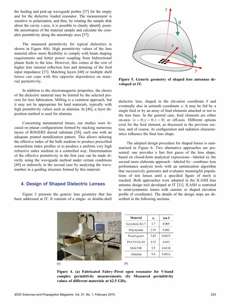
Two classical methods are used at IT for complex per-mittivity measurement: the waveguide method [55] and theopen resonator Fabry–Pérot method [56], [57]. The wave-guide method is very convenient for low to moderate permit-tivity and losses ("r up to 5 and tan � in the 10�4–10�2 range).Parallelepiped samples of the dielectric material are precisely cutto fill completely the cross section of the rectangular waveguideshort-circuited sample holder. Under single-mode TE10 condi-tions, the complex permittivity is calculated from the measureds11 frequency responses for the 1) dielectric filled and 2) emptysample holders. The method is quite accurate, provided that theair gaps between the sample and waveguide walls are less than50 �m in the V-band. Because the required samples are verysmall (typically 3:9� 1:9� 5:0 mm3 in the V-band), materialnonhomogeneity or anisotropy can be evaluated by cutting sam-ples from different parts and different orientations of the raw ma-terial block.
Excitation of higher order modes in the dielectric filledsample holder for relative permittivity values typically largerthan 5 tends to introduce significant error in the complex permit-tivity determination, particularly in the loss tangent. The Fabry–Pérot open resonator method [56] does not have this limitation.A plane-concave configuration was selected since it involvesthe fabrication of only one spherical mirror while allowingprecise positioning of the dielectric samples directly on theplanar mirror, without any perturbation from sample holders[see Figure 4(a)]. The resonator dimensions were chosen toproduce at the planar mirror a 6-mm beam waist fundamentalGaussian mode with well-defined linear polarization. Thequality factor of the empty Fabry–Pérot resonator is 106. Thecomplex permittivity of the sample dielectric material disk iscalculated from the s21 frequency response measured between
Figure 3. (a) Front side of the multiple XETS prototype close to cmscale, for 30-70 GHz operation. (b) Back side showing the Schottkydiodes and EZ-34 coaxial cables for retrieving the IF signal.
IEEE Antennas and Propagation Magazine, Vol. 57, No. 1, February 2015252
the feeding and pick-up waveguide probes [57] for the emptyand for the dielectric loaded resonator. The measurement issensitive to polarization, and thus, by rotating the sample diskabout the cavity z-axis, it is possible to clearly identify possi-ble anisotropies of the material sample and calculate the com-plex permittivity along the anisotropy axes [57].
The measured permittivity for typical dielectrics isshown in Figure 4(b). High permittivity values of the lensmaterial allow more flexibility to comply with beam shapingrequirements and better power coupling from bidirectionalplanar feeds to the lens. However, this comes at the cost ofhigher lens internal reflection loss and detuning of the feedinput impedance [37]. Matching layers [40] or multiple shelllenses can cope with this opposite dependence on mate-rial permittivity.
In addition to the electromagnetic properties, the choiceof the dielectric material may be limited by the selected pro-cess for lens fabrication. Milling is a common approach, butit may not be appropriate for hard materials, typically withhigh permittivity values such as alumina. In [46], a layer de-position method is used for alumina.
Concerning metamaterial lenses, our studies were fo-cused on planar configurations formed by stacking numerouslayers of ROGERS duroid substrate [58], each one with anadequate printed metallization pattern. This allows tailoringthe effective index of the bulk medium to produce prescribednonuniform index profiles or to produce a uniform very highrefractive index medium in a controlled way. Determinationof the effective permittivity in the first case can be made di-rectly using the waveguide method under certain conditions[49] or indirectly in the second case by analyzing the wave-number in a guiding structure formed by this material.
4. Design of Shaped Dielectric Lenses
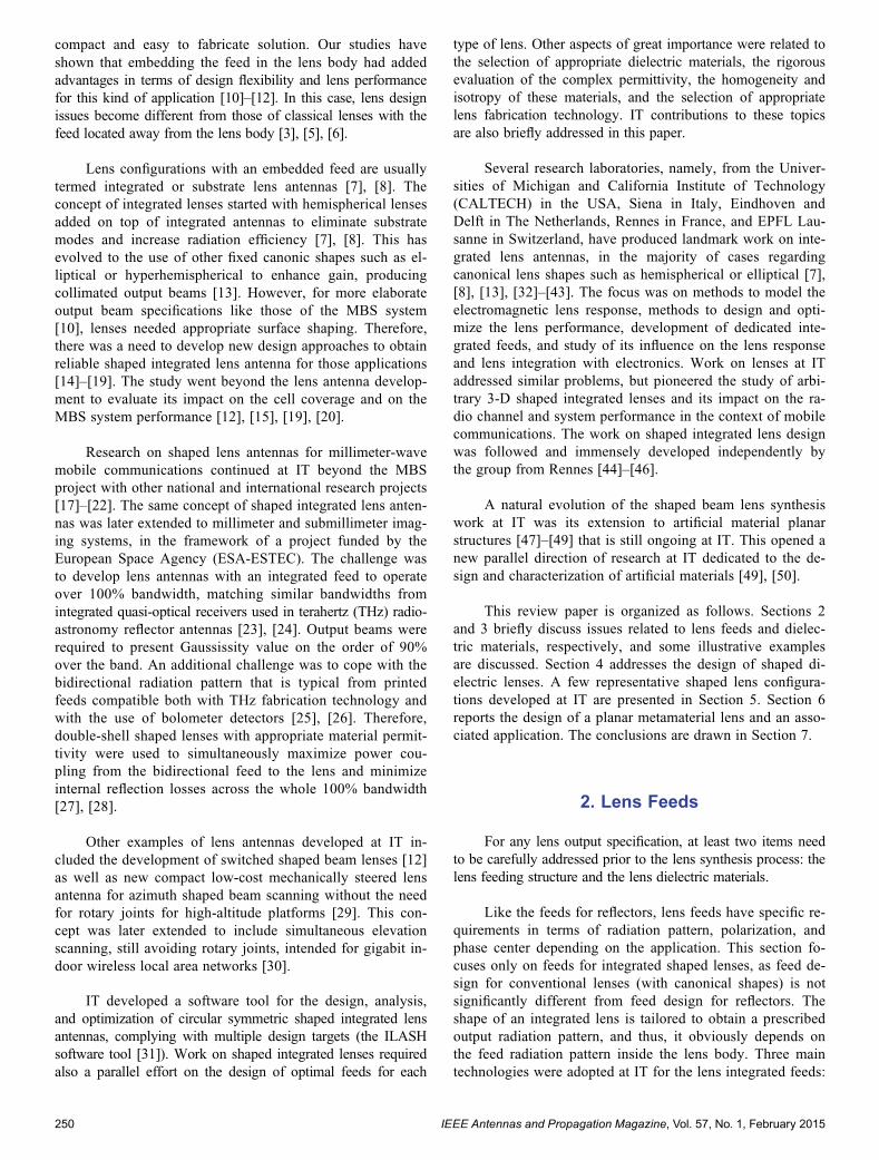
Figure 5 presents the generic lens geometry that hasbeen addressed at IT. It consists of a single- or double-shell
dielectric lens, shaped in the elevation coordinate � andeventually also in azimuth coordinate �. It may be fed by asingle feed or by an array of feed elements attached or not tothe lens base. In the general case, feed elements are eitheron-axis ðx ¼ 0; y ¼ 0; z ¼ 0Þ or off-axis. Different optionsexist for the feed element, as discussed in the previous sec-tion, and of course, its configuration and radiation character-istics influence the final lens shape.
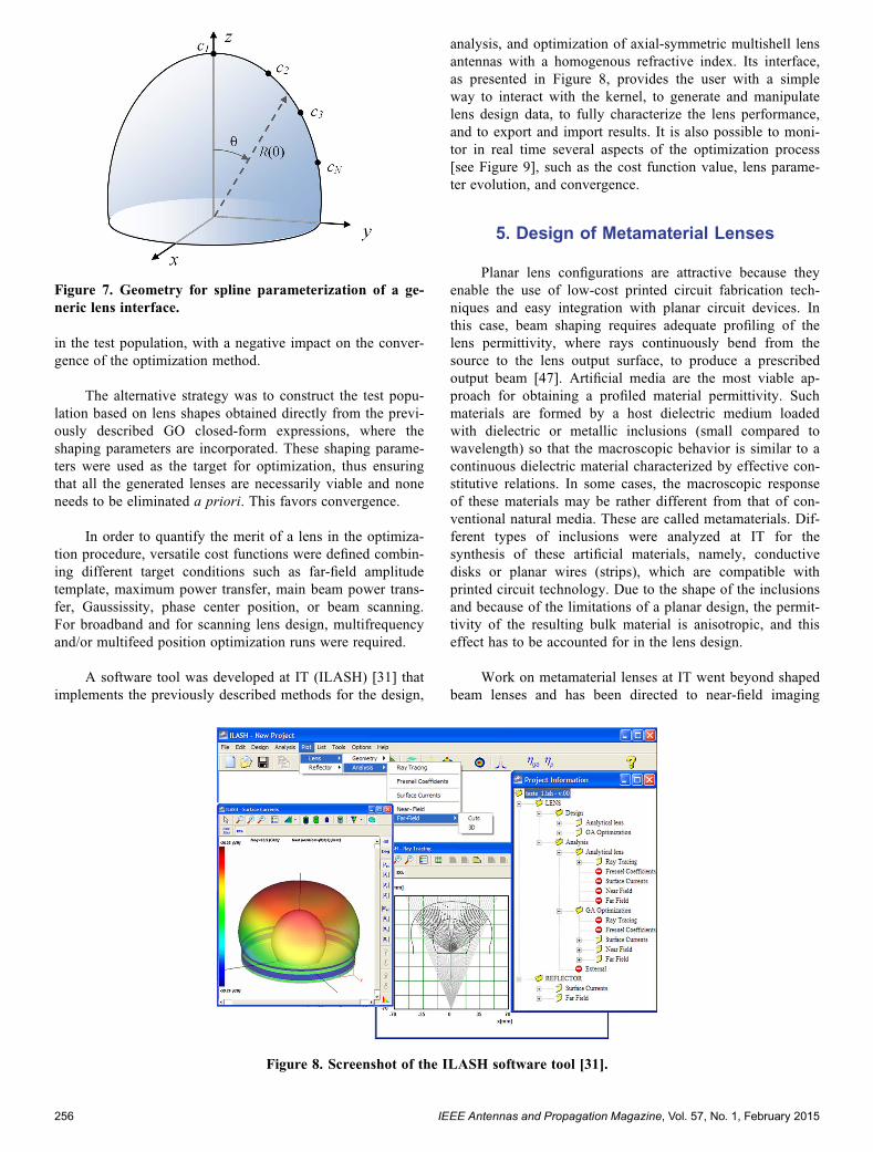
The adopted design procedure for shaped lenses is sum-marized in Figure 6. Two alternative approaches are pre-sented: one provides a fast first guess of the lens shape,based on closed-form analytical expressions—labeled a); thesecond more elaborate approach—labeled b)—combines lensperformance analysis tools with an optimization algorithmthat successively generates and evaluates meaningful popula-tions of test lenses until a specified figure of merit isreached. Both approaches were adopted in the ILASH lensantenna design tool developed at IT [31]. ILASH is restrictedto axial-symmetric lenses with canonic or shaped elevationprofile (� coordinate). The details of the design steps are de-scribed in the following sections.
Figure 4. (a) Fabricated Fabry–Pérot open resonator for V-bandcomplex permittivity measurements. (b) Measured permittivityvalues of different materials at 62.5 GHz.
Figure 5. Generic geometry of shaped lens antennas de-veloped at IT.
IEEE Antennas and Propagation Magazine, Vol. 57, No. 1, February 2015 253

4.1 Direct Lens Solutions
Closed-form lens synthesis expressions can be obtainedas a first guess for some classes of target specifications,based upon geometrical optics (GO) formulation. The lensoverall dimensions and the principal radii of curvature at ev-ery point on the surface are required to be much larger thanthe wavelength to ensure the GO validity. The feed is char-acterized only by its phase center and by its far-field patternin an unbounded medium with the same permittivity of thelens material. The GO lens designs are inherently broadbandas long as the lens dimensions are large compared to thewavelength, the material dispersion is negligible, and thefeed radiation pattern remains constant versus frequency.
The lens shape is directly determined from the solutionof a set of partial differential equations corresponding to
Snell laws at the lens interfaces and additional conditions re-lated to the output requirements. The calculation time is gen-erally on the order of seconds, which makes it attractive as afirst guess and as a seed for a subsequent refinement optimi-zation loop if required. Alternatively, the GO formulationcan include shaping parameters that enable running theclosed-form expressions in the optimization loop b) of Figure 6to match an appropriate cost function [31]. This narrows downthe search space to physically meaningful lenses.
Analytical formulations for shaped lens design weredeveloped for different output specifications and lens systemconfigurations (see Table 1). Earlier designs involved a singleoutput condition—fixed beam complying with a far-field out-put template (the target far-field radiation pattern specifica-tion). This requires just a single lens refracting surface. Bothaxis-symmetric [11], [12] and generic 3-D lenses were
Figure 6. Block diagram of lens design steps.
Table 1. Summary of All Analytical Formulations Developed at ITBased on GO for Shaped Lens Design.
IEEE Antennas and Propagation Magazine, Vol. 57, No. 1, February 2015254

developed [14], [19] to produce sec2-type elevation radiationpatterns, in some cases also with shaping in azimuth. Lateron, expressions were presented also for nonuniform refractiveindex planar lenses based on artificial dielectric media [47]–[49]. By adding a second shell to a lens, it is possible to im-pose an additional design specification. Formulations werepresented for double-shell axis-symmetric lenses combining afar-field template with a maximum power transfer condition[22] or alternatively with the specification of a well-definedphase center position [28]. These lenses were studied as highGaussissity feeds for reflectors.
Integrated lenses are also attractive for scanning or mul-tibeam applications at millimeter waves and THz. They canbe glued directly on top of an array of feeds on chip to forma compact stand-alone multibeam antenna. GO-based formu-lations were developed for double-shell axial-symmetric inte-grated lenses imposing simultaneously a reduced phaseaberration condition for off-axis feed positions and a ray col-limation condition for the beams [59], [60]. These lenses canscan up to 5 beamwidths with less than 1.5 dB gain scanloss. Integrated scanning lenses can be combined with areflector to significantly increase the output gain. In thiscase, the beam collimation condition was replaced by an-other one imposing a well-defined phase center positionlying far behind the lens body and coincident with the focusof the reflector [28]. This concept has been explored to pro-duce multiple virtual foci in the reflector focal plane using asingle lens [61], which is attractive to increase the number ofbeams using less space than conventional focal plane arrays.
A new compact and simple mechanically steered beamconcept has also been developed, starting with a closed-formformulation. The beam scanning is obtained by mechanicallymoving a specially shaped lens in front of its stationary feed,without touching it [29], [30]. This avoids the otherwiseneed for fault-prone rotary joints in long continuous usage.
A few practical examples from Table 1 are presented inmore detail in Section 6.
4.2 Shaped Lens Analysisand Optimization
The GO-based formulation discussed in the previous sec-tion is inherently independent from frequency. An appropriateanalysis method is required to evaluate the lens actual perfor-mance taking into account diffraction effects, frequency depen-dence of the feed radiation pattern, and material dispersion.
The two-step GO/physical optics (PO) method [13] iswidely used in the literature and adopted at IT to determinethe radiation pattern of lens antennas (also of reflector andother aperture antennas). It offers a very good compromisebetween quality of results and computation time, making itattractive for integration into lens design optimization loops. Ittakes as input the lens shape, the material permittivity, the
feed position, and the far-field pattern from the feed in thelens material. The GO is used for evaluating the field distribu-tion over the lens/reflector surface, and PO is used to calculateits contribution to the near- or far-field radiation. GO/PO isparticularly useful for very large structures in terms of wave-length, and there is no upper size limit for its applicability. Onthe contrary, GO fails for small lenses [62], where the feedcan no longer be replaced by its far-field radiation pattern andthe ray propagation approach is no longer valid.
An alternative formulation was developed at IT to cir-cumvent some of the indicated limitations of GO/PO in thecharacterization of small lenses [63]. It is a PO-basedmethod that uses point-like sources as basis functions to de-compose the precalculated feed aperture fields at the lensbase and calculate the resulting incident near field at thelens surface. The proposed method was implemented only foraxial-symmetric lenses with on-axis feed.
Another limitation of the GO approach is that it ignorespossible surface waves that can be excited at the lens radiat-ing interface [38]. However, our analysis showed that this ef-fect is more important in collimating lenses with canonicalshapes, such as the elliptical lens; it is imperceptible in mostof the shaped lenses designed at IT.
Full-wave numerical solvers such as the CST Micro-wave Studio transient solver [64] were used at IT to analyzethe final lens design prior to fabrication. Such tool takes intoaccount all the effects that are handled with some approxi-mations in the previously discussed methods, but due to theinvolved computation time, it is not viable option for inte-gration in lens design optimization loops.
The genetic algorithms (GA) optimization method haslong been used at IT [48] because of its flexibility, robust-ness, global search character, inherent capability to avoidtrapping in local minima, and complete absence of restric-tions on the behavior of the function to be optimized. Thedrawback is its relatively slow convergence, and hence, twodifferent approaches were used to reduce the number ofshape parameters that model the unknown lens surfaces (par-allel boxes in the b) path of Figure 6):
• spline-based representation of the lens surface;
• parametric optimization of selected parametersfrom the GO closed-form design expressions.
The spline-based representation is the most flexible ofthe two solutions, allowing for a limitless search space. Asfew as 4 to 5 nodal points cn of the lens surface are used asthe target for optimization [see Figure 7], whereas a cubicspline approximation is used to represent the lens surface be-tween consecutive pairs of these wide-spaced nodal points.Particularly with double-shell lenses, this strategy often leadsto the presence of caustics near the outer lens surface. Theselenses are automatically eliminated from the test population,but this may significantly reduce the number of “individuals”
IEEE Antennas and Propagation Magazine, Vol. 57, No. 1, February 2015 255
in the test population, with a negative impact on the conver-gence of the optimization method.
The alternative strategy was to construct the test popu-lation based on lens shapes obtained directly from the previ-ously described GO closed-form expressions, where theshaping parameters are incorporated. These shaping parame-ters were used as the target for optimization, thus ensuringthat all the generated lenses are necessarily viable and noneneeds to be eliminated a priori. This favors convergence.
In order to quantify the merit of a lens in the optimiza-tion procedure, versatile cost functions were defined combin-ing different target conditions such as far-field amplitudetemplate, maximum power transfer, main beam power trans-fer, Gaussissity, phase center position, or beam scanning.For broadband and for scanning lens design, multifrequencyand/or multifeed position optimization runs were required.
A software tool was developed at IT (ILASH) [31] thatimplements the previously described methods for the design,
analysis, and optimization of axial-symmetric multishell lensantennas with a homogenous refractive index. Its interface,as presented in Figure 8, provides the user with a simpleway to interact with the kernel, to generate and manipulatelens design data, to fully characterize the lens performance,and to export and import results. It is also possible to moni-tor in real time several aspects of the optimization process[see Figure 9], such as the cost function value, lens parame-ter evolution, and convergence.
5. Design of Metamaterial Lenses
Planar lens configurations are attractive because theyenable the use of low-cost printed circuit fabrication tech-niques and easy integration with planar circuit devices. Inthis case, beam shaping requires adequate profiling of thelens permittivity, where rays continuously bend from thesource to the lens output surface, to produce a prescribedoutput beam [47]. Artificial media are the most viable ap-proach for obtaining a profiled material permittivity. Suchmaterials are formed by a host dielectric medium loadedwith dielectric or metallic inclusions (small compared towavelength) so that the macroscopic behavior is similar to acontinuous dielectric material characterized by effective con-stitutive relations. In some cases, the macroscopic responseof these materials may be rather different from that of con-ventional natural media. These are called metamaterials. Dif-ferent types of inclusions were analyzed at IT for thesynthesis of these artificial materials, namely, conductivedisks or planar wires (strips), which are compatible withprinted circuit technology. Due to the shape of the inclusionsand because of the limitations of a planar design, the permit-tivity of the resulting bulk material is anisotropic, and thiseffect has to be accounted for in the lens design.
Work on metamaterial lenses at IT went beyond shapedbeam lenses and has been directed to near-field imaging
Figure 7. Geometry for spline parameterization of a ge-neric lens interface.
Figure 8. Screenshot of the ILASH software tool [31].
IEEE Antennas and Propagation Magazine, Vol. 57, No. 1, February 2015256

lenses as well. With this purpose, much work was devoted tothe characterization of a new medium consisting of an ultra-dense array of finite-length nonconnected crossed metallicwires—the crossed-wire media [50]. It was shown that a slabmade of this material could present extreme values of the ef-fective refraction index and support tightly bound surfacewave modes, with very fast field decay in the transversalplane. These near-field evanescent waves can be used to re-store the fine details of an object in the vicinity of the lens,beating the Rayleigh �=2 diffraction limit [65], [66]. Al-though this topic of superlensing is widely addressed in theliterature, our work brought important new features that aredescribed in one of the examples from Section 6.
5.1 Case of Shaped Beam Lenses
The design of shaped beam metamaterial lenses at IT wasrestricted to axis-symmetric cases with a single output conditionspecification: the far-field amplitude template. Due to the axialsymmetry, the problem could be solved in a single cross
section of the lens. The design procedure comprises two mainsteps: one is related to the determination of the permittivity pro-file, assumed as a continuous function of space coordinates; thesecond step corresponds to the determination of the spatial dis-tribution of inclusion sizes that are required to match the pre-scribed permittivity profile [see Figure 10].
The lens medium is described by a coordinate-dependentpermittivity tensor reflecting the anisotropy that is due to theshape and orientation of the selected inclusion. The GO formu-lation [67] is used to calculate the required spatial profile of thepermittivity. As aforementioned, because of the selected inclu-sions and of the adopted layout [47]–[49], the resulting mediumis uniaxial. Thus, with appropriate feed polarization, the un-known reduces to a single element of the permittivity tensor,and it only depends on a single coordinate.
A system of differential equations obtained from a suit-able Hamiltonian [67] describes the ray trajectory as a func-tion of the unknown permittivity profile. An additionaldifferential equation establishes the relation, which dependson the unknown permittivity profile, between the output
Figure 9. GA optimization monitoring screen [31].
Figure 10. (a) Geometry of planar lens formed by stacking printed cir-cuit boards. (b) Sample of disk media for measurement of effectivepermittivity.
IEEE Antennas and Propagation Magazine, Vol. 57, No. 1, February 2015 257

angle �f of each ray trajectory and the corresponding shoot-ing angle �0 that is required to transform the feed power pat-tern to the prescribed output far-field power template. Thepermittivity function is then inverted in closed form or nu-merically to satisfy simultaneously the pertinent differentialequations [47]. Alternatively, the inversion step can be re-placed by an optimization loop where the unknown permit-tivity profile is represented by a polynomial function and itscoefficients are then optimized in a loop, solving repeatedlythe direct problem until a satisfactory solution is found [48].
Once the permittivity profile is known, the required ma-terial must be synthesized. The effective permittivity of theartificial medium depends on the volume fraction that isfilled with the inclusions. The relation between the effectivepermittivity and the size of the particles has been calculatedby many authors for different types of inclusions [68].
5.2 Near-Field Imaging Lens
As previously mentioned, a crossed-wire metamaterialslab was used at IT for microwave near-field imaging. Ingeneral terms, this metamaterial can be regarded as an aniso-tropic dielectric slab waveguide, characterized by homoge-nized material constitutive parameters. However, due to thefact that the inclusions (continuous metallic wires) arespanned over many unit cells of the material, classical ho-mogenization methods for unbounded bulk media are notvalid for these structures [50], and classical boundary condi-tions are incomplete to describe the fields at the interfaces.The authors have demonstrated a new modified homogeniza-tion procedure with modified boundary conditions that canaccurately characterize the reflection and transmission ofwaves by thin metamaterial slabs, remaining valid for wideincident angles and for evanescent waves [69]. Interestingly,the new approach requires just the knowledge of the un-bounded bulk medium material properties but adds accuracyto the description of wave interaction with metamaterialslabs of arbitrary thickness.
After the transmission coefficient through the slab isobtained for a plane incident wave, the structure parameters(slab thickness and wire lattice constant) are optimized to en-hance the excitation of guided evanescent waves while mini-mizing the excitation of guided propagating waves. Whileimage resolution based on propagating waves is bounded bythe �=2 diffraction limit, evanescent waves can retain sub-lambda details in the near field. Since the size of the wires ismuch smaller than the wavelength, the effect is nonresonant,and it holds for a reasonable bandwidth.
6. Examples of Developed Lenses
This section presents selected lens examples out from alarge collection developed over the years at IT for different
applications. These and other examples are discussed in fulldetail by the authors in the indicated references.
6.1 Shaped Lens for Wireless MobileBroadband Communications
The cellular MBS concept was introduced in 1992 anddeveloped throughout the 1990s [9]. It was intended to trans-port, in a transparent way, asynchronous transfer mode cellsover the air interface at data rates up to 155 Mb/s, withstand-ing mobile velocities up to 100 km/h, while maintaining thequality of service of the fixed network. Provisional subbandswere allocated for these systems at 39.5–40.5, 42.5–43.5GHz and 62–63, 65–66 GHz.
At the base station, a shaped beam was required to ap-proximate a constant flux illumination of the cell to favor thelink budget, with a reasonably sharp drop at the cell edge tocontrol cell spillover [see Figure 11(a)]. This characteristiccorresponds to csc2 �-type gain contribution from the anten-nas to the link budget within the cell, which ideally compen-sates for the free-space loss at each observation direction.An acrylic 3-D lens was designed using a modification ofGO closed-form expressions to produce constant flux illumi-nation across a long street section when hanging from alamp post located 10 m above the street level at the center ofthe cell [21]. The lens was fed by the embedded open-endaperture of a dielectric loaded rectangular waveguide oper-ating in the TE10 mode. The lens prototype is shown inFigure 11(b) [10], [21]. The dimensions are 10� 4� 2 cm3,and the lens produces a bidirectional radiation pattern with13.2 dBi gain at 62.5 GHz at the maximum distance direc-tion ð�max; ’ ¼ �90�Þ, with linear polarization [10]. Thelens was successfully used in an outdoor system demonstra-tor operating at a 32 Mb/s gross bit rate [16]. In a follow-upproject, these lenses were redesigned for the 40-GHz bandwith the same specification but using a lower loss dielectricmaterial, i.e., polystyrene [15]. A similar radiation patternwas obtained in this case, but with slightly higher gain of14 dBi. The received power over the street cell is plotted inFigure 11(c). It shows that by using a single shaped lensantenna at the center of the cell, it is possible to produce arectangular type of coverage above the threshold level, almostconfined to the cell limits. No similar type of performance hasbeen presented before for any antenna.
In a different configuration, a 3-D lens was developedto produce a constant flux illumination with sharp squareboundaries, appropriate for indoor room coverage with con-trolled wall illumination, as shown in Figure 12(a) [19]. Thelens was made of acrylic with the size 84� 32 mm2 (diago-nal × depth) for operation at 62.5 GHz. The lens was fed bythe circularly polarized TE11 mode of a circular waveguideimmersed in the lens body and mounted near the ceiling.Figure 12(b) shows the received power distribution beneaththe lens, measured while the receiving lens antenna, with aflat-topped radiation pattern [15], traveled on a kart to scan a
IEEE Antennas and Propagation Magazine, Vol. 57, No. 1, February 2015258

4� 8 m2floor area. The difference in height between the
base station and the mobile terminal antenna was 0.5 m. Thefigure shows a constant received power in the illuminatedregion and a sharp drop at the cell edge as required. Thesec2 radiation pattern has the interesting property that thecell dimensions can be scaled just by changing the heightdifference between the fixed and the mobile antennas. Thistopic is further developed in [19], where the calculated andmeasured radiation patterns, as well as the resulting channeltime dispersion characteristic, are given.
6.2 Multibeam Lens Antennas
The first example refers to an integrated multibeam lensantenna intended to produce 3 dB beamwidths on the orderof 6° at the 60-GHz band, with high Gaussissity, gain scanloss lower than 1 dB over �20� scan angle, and comply-ing with a maximum diameter of 70 mm [59]. The lens
was required to operate over 40% bandwidth, and thus, thechallenge was to minimize internal reflections and to ensurea reasonably stable Gaussian beam shape across the scannedangular interval.
A double-shell configuration was adopted to allow impos-ing both a beam collimation condition and the Abbe sine con-dition to minimize aberration of the output beam. The selectedlens materials were the MACOR/acrylic combination (permit-tivity 5.5/2.53), and the feed was the especially designedwaveguide aperture described in Section 2 for 62.5-GHzoperation. Figure 13(a) shows the lens antenna prototype thatwas designed using ILASH [31]. The lens dimensions are60 mm in diameter at the base and 37 mm in height; theouter shell material is transparent, and thus, it reveals theinner shell, which appears distorted due to refraction effects.The dedicated waveguide feeds from Section 2 were used for-convenience of the measurement setup, which is based on awaveguide.
Figure 12. (a) Dielectric lens antenna for a square cell fed by a circular wave-guide. (b) Received power distribution measured in the laboratory at 62.5 GHz.
Figure 11. (a) Geometry of a street sectored cell. (b) Photograph of a shaped lensantenna for a constant flux illumination of the street at 60 GHz. (c) Receivedpower within the cell limits for a transmitted power of 22 dBm.
IEEE Antennas and Propagation Magazine, Vol. 57, No. 1, February 2015 259

Figure 13(b) shows the measured and simulated radia-tion pattern results for different feed positions at 1.1-mmsteps along the lens base in the H-plane. This produces over-lapping of consecutive beams near the −1.5 dB level with re-spect to maximum. Beam overlap at −3 dB occurs for widerseparation between consecutive feeds, compatible with theused feed aperture size (not shown). The figure shows excel-lent agreement between ILASH predictions and measure-ments and confirms the effectiveness of the proposeddouble-shell lens concept regarding beam scan linearity, in-ternal reflections, beam shape, and Gaussissity preservationwith extremely low scan loss up to 20° elevation. Theachieved gain was on the order of 18–19 dBi, and the scanloss was better than 1 dB for 43–62 GHz. As a consequenceof the GO-based lens design, the scan angle dependence onthe feed off-axis position was practically independent of fre-quency, and the beam Gaussissity was better than 95%.
The following example is intended to demonstrate theviability of the wideband XETS printed antenna with a sim-ple integral mixer described in Section 2 as an integratedmultibeam lens feed and to show the effectiveness of the IFsignal retrieval setup. Despite the tightly packed assembly ofthe XETS elements at the lens base, the proposed feed still
offers good isolation between adjacent elements both at RFand IF, providing very stable radiation pattern and linear po-larization over the bandwidth.
The above objectives can be demonstrated using just acanonic single material lens, but the conclusions remain validfor more sophisticated lens design. A 68-mm-diameter MA-COR elliptical lens was used in this case, as shown in Figure14(a) [54]. The lens was designed to scan the angular intervalfrom 0 to �18� with beam overlap approximately at −3 dB for43 GHz and at −4.5 dB for 62.5 GHz. The overlap level at thehigher frequencies could have been improved with other lensdesigns, but this type of optimization exceeded the establishedobjective for this example.
The radiation pattern measurement configuration is shownin Figure 14(b). The Schottky diode integrated into the XETSreceives both the 62.5-GHz far-field TX signal (through thelens) and the 64-GHz LO signal (through the air from the back),producing the desired 1.5-GHz IF signal. The LO assembly isfixed with respect to the lens, so that the LO signal amplitudeilluminating the XETS does not change with lens rotation,whereas the IF signal amplitude changes only in response tolens radiation pattern at the TX frequency.
Figure 13. (a) Fabricated MACOR/acrylic lens prototype, showing the attached60-GHz band waveguide feed. (b) Simulated and measured gain radiation patternsat 62.5 GHz, in the H-plane, with feed at 0, 1.1, 2.2, 3.3, 4.4, and 5.5 mm from thelens axis [31].
Figure 14. (a) Bottom view of a MACOR elliptical lens fed by a multi-XETSassembly with an integrated mixer. (b) Radiation pattern measurement setup at62.5 GHz, using an integrated mixer at the base of the lens.
IEEE Antennas and Propagation Magazine, Vol. 57, No. 1, February 2015260

Examples of the H-plane measured and simulated radia-tion patterns are depicted in Figure 15 at 62.5 GHz for threeXETS elements (x ¼ 2 mm, x ¼ 3 mm, and x ¼ 6 mm). Thecurves are normalized to the respective maximum. The mainlobe shape is quite stable, with the correct beam inclinationdespite the very close position of the XETS elements. Cross-polar level is below −15 dB, which is much better than whatcan be obtained, for instance, with the self-complementarylog-periodic feed. This validates the expected feed perfor-mance. The only inconvenience of this feed is that, onceglued at the lens base, it can no longer be reused.
6.3 Broadband Lens as a Primary Feedfor Reflectors
A double-shell shaped dielectric lens with five inte-grated feeds at its base was designed to illuminate a 90° off-set reflector with slightly less than 2� separation betweenfocal points, for 3 dB adjacent beam rollover. The lens out-put beams for each embedded feed produce a virtual focuslocated far below the lens and close to the corresponding re-flector focal points [see Figure 16(a)]. The parabola rotatesabout an axis passing through the lens axis for mechanicalbeam scan in azimuth, whereas the lens provides multiple
beam coverage in elevation. The challenge was to match theabove requirements along with stable scanning characteris-tics, transmission efficiency, and aperture efficiency over thespecified 1:3 bandwidth.
The shaped double-shell dielectric lens antenna was de-signed by imposing simultaneously a well-defined phase cen-ter located below the lens body and an aberration condition,as shown in Figure 16(b) [28]. The 20� diameter lens proto-type was made of MACOR and acrylic and was fed by thewaveguide feed described in Section 2 with a special fixtureto allow its precise positioning at different positions at thelens base. The lens performance in terms of radiation patternand phase center measured at 43 and 62.5 GHz agreed verywell with the specifications [28]. The lens output beamGaussissity was better than 94% over the band.
The performance of the lens–reflector assembly wassimulated using the ILASH GO/PO module. The reflector ra-diation pattern at 62.5 GHz is presented in Figure 17(a)showing well-defined beams with maximum 1.6 dB scanloss. Figure 17(b) shows for the central beam that the aper-ture efficiency is practically constant versus frequency, andin agreement with that property, the directivity in decibelsincreases almost linearly with frequency.
Figure 15. Comparison between simulated and measured radiation patterns at 62.5 GHz in the H-plane for a feed dis-placement of (a) x ¼ 2 mm, (b) x ¼ 3 mm, and (c) x ¼ 6 mm.
Figure 16. (a) Problem geometry. (b) Fabricated lens prototype with aMACOR inner shell and an acrylic outer shell.
IEEE Antennas and Propagation Magazine, Vol. 57, No. 1, February 2015 261

In a second example, the objective was to design a focalplane feed for a reflector such that the reflector radiation patternhas a frequency independent beamwidth over 1:3 bandwidth.It is known that the larger the reflector illuminated area is, thenarrower is its radiation pattern. Hence, the reflector feed is re-quired to have an increasing directivity for increasing frequen-cies. Simultaneously, it must exhibit a stable phase center acrossthe whole band. The reflector is based on a 90° offset configura-tion with focal length F ¼ 3 m and projected aperture diameterD ¼ 2:5 m. A 70-mm-diameter double-shell collimated beamlens was designed using the MACOR/acrylic material com-bination, as shown in Figure 18(a) [27]. The performance of theisolated lens was experimentally characterized at 43 and62.5 GHz using the waveguide feeds described in Section 2that provide a very similar radiation pattern at the two fre-quencies. The combined lens plus reflector performance wasevaluated by simulation using ILASH. The reflector radia-tion pattern for different frequencies is shown in Figure 18b.Despite some variation of the lens phase center with frequency,its impact on the reflector directivity is not significant. It is onthe order of 56 dBi within the considered band, with a variationof ±0.5 dB. It is noted, however, that the success of the designis limited by the condition that the feed radiation pattern is con-stant over the band and that lens dissipation losses are very low,
so that its frequency behavior is not manifested in the reflectorgain characteristic.
6.4 Mechanical Beam-Steering Lenses
A new lens antenna configuration was proposed by the au-thors in [29] for low Earth orbit satellite data link communica-tions at 26 GHz. The lens was required to produce a sector beamwith shaping in elevation and to enable a simple mechanical az-imuth scanning. The target gain versus elevation angle � is givenapproximately by secðk�Þ. With an appropriate choice of the kshaping parameter, this elevation radiation pattern compensatespath-loss attenuation taking into account the Earth’s curvature.
The designed shaped lens is axial symmetric, but a spheri-cal air cavity is excavated through its base at a calculated offsetdistance with respect to the lens symmetry axis [see Figure 19(a)]. The feed aperture is at the center of this spherical air cavity.The asymmetry introduced by the feed position produces anadequate directive shaped beam [see Figure 19(b)]. This is an ex-tremely simple solution where the feed is fixed and the lens ro-tates about the feed axis to provide the required beam scanning.
Figure 17. a) Radiation pattern of the reflector when illuminated by the fabricatedlens prototype, with an inner shell of MACOR and an outer shell of acrylic. (b) Cal-culated directivity and aperture efficiency of the reflector for the central beam.
Figure 18. (a) Fabricated MACOR/acrylic lens prototype, showing the attached 60-GHzband waveguide feed. (b) Simulated radiation patterns of the reflector fed by the lens.
IEEE Antennas and Propagation Magazine, Vol. 57, No. 1, February 2015262

The feed is not in physical contact with the lens, thus avoidingthe need for fault-prone rotary joints in long continuous usage.The assembly is very compact and lightweight (lens diameteris less than five wavelengths, and height is less than threewavelengths) complying with mass and volume restrictionsfor satellites.
The same concept of a moving lens with fixed feed wasextended for azimuth plus elevation mechanical scanning ina different application context. Wireless indoor transmissionof an uncompressed high-definition (HD) video signal be-tween a video device such as a camcorder and an HD TVdisplay may soon become a requirement for mass markethome applications. The WirelessHD standard [70] proposesto use the unlicensed spectrum from 57 to 66 GHz for suchapplications. For mass consumer applications, the radio linkmust use inexpensive low-power sources, and hence, highgain antennas (>20 dBi) are required to favor the link bud-get. The narrow beam needs to be steered to allow for theuser mobility. A new configuration of a mechanical steerablebeam antenna has been developed at IT where a dielectriclens pivots in front of a single stationary moderate gain feed,as shown in Figure 20(a) [30]. Again, the feed is not inphysical contact with the lens. As discussed previously, thiseliminates the need for rotary joints and the associated draw-backs. The designed lens is made of polyethylene and is
such that both the input and output lens surfaces are shapedto accommodate a beam collimation condition and a scan anglemaximization condition. The lens output beam is aligned withthe lens axis for all lens orientations within the operation cone.Thus, pivoting the lens around two of its main axis allowssteering the beam in elevation and azimuth. The important dif-ference with respect to conventional scanning lenses is that, forall inclinations of the lens, the focus is always exactly coinci-dent with the aperture phase center. In this way, aberrations arestrongly reduced, allowing wider scan angles than conventionalsolutions. The fabricated lens assembly demonstrated a �45�
to þ45� elevation scan capability over full azimuth, with 21 dBgain and better than −1.1 dB gain scan loss [see Figure 20(b)].The radiation efficiency was always above 95%. A simple sys-tem demonstrator has been recently assembled to prove the fea-sibility of the antenna concept, of the tracking mechanism, andits algorithms [71].
6.5 Near-Field Lens Operatedin Backscattering Mode
Next, we report some of our findings in the area ofnear-field lensing. In this context, the main challenge is toproduce a very localized beam spot that can be used to probe
Figure 19. (a) MACOR axial-symmetric 50-mm-diameter shaped lens. (b) Radiationperformance (in polar coordinates) of the lens computed with the GO/PO method.
Figure 20. (a) Photograph of the manufactured polyethylene lens plus horn feed.(b) Measured radiation patterns of the lens antenna for several lens tilt angles.
IEEE Antennas and Propagation Magazine, Vol. 57, No. 1, February 2015 263
subwavelength details of an object or to detect very closelyspaced objects. This can be interesting for many applications,which include subwavelength imaging, detection of buried tar-gets, microwave heating, etc. To manipulate and resonantlyinteract with the near field, one can rely on metamaterials.Near-field lenses made of metamaterials have been extensivelystudied in recent years. Some examples include wire medialenses [72]–[74], high-pass spatial filtering lenses [75] basedon magnetoinductive waves [76], lenses made of left-handedmaterials and negative permittivity materials [77]–[80], hyper-bolic media lenses [81], [82], and structures relying on radia-tionless electromagnetic interference [83]–[86].
We have demonstrated in [84] that materials with anextremely large and positive index of refraction may providean interesting solution to collimate the near field, preventinga lateral spreading of the beam. Such materials may be im-plemented in practice based on the crossed-wire medium me-tamaterial. We have shown that a dense metallic mesh ofnonconnected crossed wires can support guided modes asso-ciated with extremely short guided wavelengths, and theseguided modes may be resonantly coupled to the near field,somewhat analogous to surface plasmon polaritons [85],[86]. Because of these properties, a thin slab of our metama-terial “superlens” may enhance subwavelength features inac-cessible with conventional systems [84].
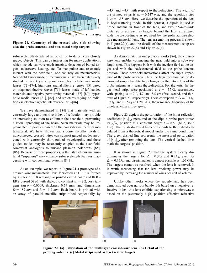
As an example, we report in Figure 21 a prototype of acrossed-wire metamaterial lens fabricated at IT. It is formedby a stack of 308 rectangular printed circuit boards of ROG-ERS duroid 5880 with dielectric constant "r ¼ 2:2, loss tan-gent tan � ¼ 0:0009, thickness 0.79 mm, and dimensionsD ¼ 182 mm and L ¼ 11:7 mm. Each board is printed withan array of parallel metallic strips tilted sequentially by
�45� and þ45� with respect to the z-direction. The width ofthe printed strips is ws ¼ 0:247 mm, and the repetition stepis � ¼ 1:58 mm. Here, we describe the operation of the lensin backscattering mode. In this context, a dipole is used asprobe antenna in front of the lens, and two 2.5-mm-widemetal strips are used as targets behind the lens, all alignedwith the x-coordinate as required by the polarization-selec-tive metamaterial lens. The lens assembling process is shownin Figure 22(a), and the details of the measurement setup areshown in Figure 22(b) and Figure 22(c).
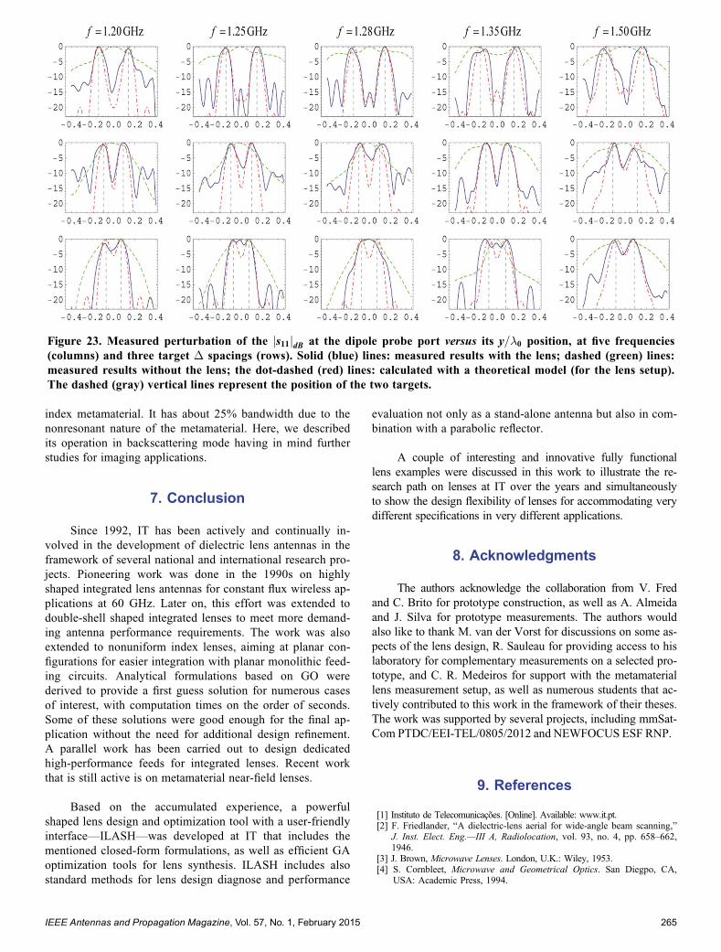
As demonstrated in our previous works [84], the crossed-wire lens enables collimating the near field into a subwave-length spot. This happens both with the incident field at the tar-get and with the backscattered field at the probe antennaposition. These near-field interactions affect the input imped-ance of the probe antenna. Thus, the target position can be de-termined simply by detecting changes on the return loss of theprobe antenna as it scans the x-direction. For the tests, the tar-get metal strips were positioned at z ¼ �3L=2, successivelywith spacing � ¼ 7:0, 4.7, and 3.5 cm (first, second, and thirdrows of Figure 23, respectively). These correspond to � ¼ 0:3�0,0:2�0, and 0:15�0 at 1.28 GHz, the resonance frequency of thedipole antenna in free space.
Figure 23 depicts the perturbation of the input reflectioncoefficient js11jdB measured at the dipole probe port versusits y=�0 position at a constant height z ¼ 0:5L (blue, solidline). The red dash-dotted line corresponds to the E-field cal-culated from a theoretical model under the same conditions.The green dashed line represents the measured perturbationof js11jdB after removing the lens. The vertical dashed linesmark the targets’ position.
It is shown in Figure 23 that the system clearly dis-criminates the targets for � ¼ 0:3�0 and 0:2�0, even for� ¼ 0:15�0, and discrimination is almost possible at 1.20 GHz.The targets cannot be resolved when the lens is removed. Itis worth mentioning that the lens resolving power may beimproved by increasing the number of wires per unit of volume.
Unlike other works where the superlensing has beendemonstrated over narrow bandwidth based on a negative re-fractive index, this lens exhibits superlensing at microwavesbased on the (extremely high) positive effective refractive
Figure 21. Geometry of the crossed-wire slab showingalso the probe antenna and two metal strip targets.
Figure 22. (a) Fabrication of the multilayer crossed-wire lens. (b) Detail of theprobing antenna. (c) Metal strips used as backscatter targets.
IEEE Antennas and Propagation Magazine, Vol. 57, No. 1, February 2015264
index metamaterial. It has about 25% bandwidth due to thenonresonant nature of the metamaterial. Here, we describedits operation in backscattering mode having in mind furtherstudies for imaging applications.
7. Conclusion
Since 1992, IT has been actively and continually in-volved in the development of dielectric lens antennas in theframework of several national and international research pro-jects. Pioneering work was done in the 1990s on highlyshaped integrated lens antennas for constant flux wireless ap-plications at 60 GHz. Later on, this effort was extended todouble-shell shaped integrated lenses to meet more demand-ing antenna performance requirements. The work was alsoextended to nonuniform index lenses, aiming at planar con-figurations for easier integration with planar monolithic feed-ing circuits. Analytical formulations based on GO werederived to provide a first guess solution for numerous casesof interest, with computation times on the order of seconds.Some of these solutions were good enough for the final ap-plication without the need for additional design refinement.A parallel work has been carried out to design dedicatedhigh-performance feeds for integrated lenses. Recent workthat is still active is on metamaterial near-field lenses.
Based on the accumulated experience, a powerfulshaped lens design and optimization tool with a user-friendlyinterface—ILASH—was developed at IT that includes thementioned closed-form formulations, as well as efficient GAoptimization tools for lens synthesis. ILASH includes alsostandard methods for lens design diagnose and performance
evaluation not only as a stand-alone antenna but also in com-bination with a parabolic reflector.
A couple of interesting and innovative fully functionallens examples were discussed in this work to illustrate the re-search path on lenses at IT over the years and simultaneouslyto show the design flexibility of lenses for accommodating verydifferent specifications in very different applications.
8. Acknowledgments
The authors acknowledge the collaboration from V. Fredand C. Brito for prototype construction, as well as A. Almeidaand J. Silva for prototype measurements. The authors wouldalso like to thank M. van der Vorst for discussions on some as-pects of the lens design, R. Sauleau for providing access to hislaboratory for complementary measurements on a selected pro-totype, and C. R. Medeiros for support with the metamateriallens measurement setup, as well as numerous students that ac-tively contributed to this work in the framework of their theses.The work was supported by several projects, including mmSat-Com PTDC/EEI-TEL/0805/2012 and NEWFOCUS ESF RNP.
9. References
[1] Instituto de Telecomunicações. [Online]. Available: www.it.pt.[2] F. Friedlander, “A dielectric-lens aerial for wide-angle beam scanning,”
J. Inst. Elect. Eng.—III A, Radiolocation, vol. 93, no. 4, pp. 658–662,1946.
[3] J. Brown, Microwave Lenses. London, U.K.: Wiley, 1953.[4] S. Cornbleet, Microwave and Geometrical Optics. San Diegpo, CA,
USA: Academic Press, 1994.
Figure 23. Measured perturbation of the js11jdB at the dipole probe port versus its y=�0 position, at five frequencies(columns) and three target � spacings (rows). Solid (blue) lines: measured results with the lens; dashed (green) lines:measured results without the lens; the dot-dashed (red) lines: calculated with a theoretical model (for the lens setup).The dashed (gray) vertical lines represent the position of the two targets.
IEEE Antennas and Propagation Magazine, Vol. 57, No. 1, February 2015 265

[5] J. Lee, “Lens antennas,” Chapter 16 in Antenna Handbook—Theory, Ap-plications and Design, Y. T. Lo and S. W. Lee, Eds., New York, NY,USA: Van Nostrand, 1988.
[6] C. Sletten, Reflector and Lens Antenna. Norwood, MA, USA: ArtechHouse, 1988.
[7] D. B. Rutledge and M. S. Muha, “Imaging antenna arrays,” IEEE Trans.Antennas Propag., vol. AP-30, no. 4, pp. 535–540, Jul. 1982.
[8] G. Rebeiz, “Millimeter-wave and terahertz integrated circuit antennas,”Proc. IEEE, vol. 80, no. 11, pp. 1748–1770, Nov. 1992.
[9] L. Fernandes, “Developing a system concept and technologies for mo-bile broadband communications,” IEEE Pers. Commun. Mag., vol. 2,no. 1, pp. 54–59, Feb. 1995.
[10] C. Fernandes, P. Francês, and A. Barbosa, “Shaped coverage of elon-gated cells at millimetre waves using a dielectric lens antenna,” in Proc.EMC, Bologna, Italy, Sep. 1995, vol. 1, pp. 66–70.
[11] D. Lemaire, C. Fernandes, P. Sobieski, and A. Barbosa, “A method toovercome the limitations of G.O. in the design of axis-symmetrical lenses,”Int. J. Infrared Millim., vol. 17, no. 8, pp. 1377–1390, Aug. 1996.
[12] C. Fernandes, “Shaped dielectric lenses for wireless millimeter-wave communications,” IEEE Antennas Propag. Mag., vol. 41, no. 5,pp. 141–150, Oct. 1999.
[13] D. Filipovic, S. Gearheart, and G. Rebeiz, “Double-slot antennas onextended hemispherical and elliptical silicon dielectric lenses,” IEEETrans. Microw. Theory Tech., vol. 41, no. 10, 1738–1749, Oct. 1993.
[14] C. Salema, C. Fernandes, and R. Jha, Solid Dielectric Horns, Boston,MA, USA: Artech House, ch. 7, 1998.
[15] C. Fernandes, “Shaped-beam antennas,” in Handbook of Antennas inWireless Communications, L. Godara, Ed., New York, NY, USA: CRCPress, ch. 152001.
[16] J. Zubrzycki, “Mobile broadband system—A report on the work of raceproject 2067,” British Broadcasting Corporation RD 1996/12, 1996.[Online]. Available: http://archive.org/details/bbc-rd-reports-1996-12.
[17] A. Plattner, B. Byzery, C. Femandes, and T. Karttaavi, “A compact por-table 40 GHz transceiver for the mobile broadband system,” in Proc.ACTS Mobile Commun. Summit, Rhodes, Greece, Jun. 1998, pp. 843–848.
[18] M. Prögler, “SAMBA: A mobile broadband enabler,” in Proc. Eur. Microw.Conf., Munich, Germany, Oct. 1999, pp. 87–90.
[19] C. Fernandes and L. Anunciada, “Constant flux illumination of squarecells for mm-wave wireless communications,” IEEE Trans. Microw.Theory Tech., vol. 49, no. 11, pp. 2137–2141, Nov. 2001.
[20] C. Fernandes and J. Fernandes, “Performance of lens antennas in wire-less indoor millimeter-wave applications,” IEEE Trans. Microw. TheoryTech., vol. 47, no. 6, pp. 732–737, Jun. 1999.
[21] C. Fernandes, “Design of shaped lenses for non-symmetric cells inMBS,” in Proc. IEEE Int. Symp. Antennas Propag., Orlando, FL, USA,Jul. 1999, pp. 2440–2443.
[22] M. Silveirinha and C. Fernandes, “Shaped double-shell dielectric lensesfor wireless millimetre wave communications,” in Proc. IEEE Int. Symp.Antennas Propag., Salt Lake City, UT, USA, 2000, pp. 1674–1677.
[23] P. Siegel, “THz instruments for space,” IEEE Trans. Microw. TheoryTech., vol. 55, no. 11, pp. 2957–2965, Nov. 2007.
[24] A. Semenov, G. Gol’tsman, and R. Sobolevski, “Hot-electron effect insuperconductors and its application for radiation sensors,” Supercond.Sci. Technol., vol. 15, no. 4, pp. R1–R16, Apr. 2002.
[25] L. Liu et al., “Development of integrated terahertz broadband detectorsutilizing superconducting hot-electron bolometers,” IEEE Trans. Appl.Supercond., vol. 19, no. 3, pp. 282–286, Jun. 2009.
[26] A. Semenov et al., “Terahertz performance of integrated lens anten-nas with a hot-electron bolometer,” IEEE Trans. Microw. Theory Tech.,vol. 55, no. 2, pp. 239–247, Feb. 2007.
[27] E. Lima, J. Costa, and C. Fernandes, “Broadband reflector fed by in-tegrated lens antenna with frequency constant directivity,” in Proc.IEEE Int. Symp. Antennas Propag., Toronto, OM, Canada, Jul. 2010,pp. 1–4.
[28] C. Fernandes, E. Lima, and J. Costa, “Broadband integrated lens forilluminating reflector antenna with constant aperture efficiency,” IEEETrans. Antennas Propag., vol. 52, no. 12, pp. 3805–3813, Dec. 2010.
[29] J. Costa et al., “Compact Ka-band lens antennas for LEO satellites,” IEEETrans. Antennas Propag., vol. 56, no. 6, pp. 1251–1268, May 2008.
[30] J. Costa, E. Lima, and C. Fernandes, “Compact beam-steerable lensantenna for 60 GHz wireless communications,” IEEE Trans. AntennasPropag., vol. 57, no. 10, pp. 2926–2933, Oct. 2009.
[31] E. Lima, J. Costa, M. Silveirinha, and C. Fernandes, “ILASH—Software tool for the design of integrated lens antennas,” in Proc.IEEE Int. Symp. Antennas Propag., San Diego, CA, USA, Jul. 2008,pp. 1–4.
[32] M. van der Vorst, P. de Maagt, and M. Herben, “Matching layers for in-tegrated lens antennas,” in Proc. JINA, Nice, France, 1996, pp. 511–515.
[33] A. Neto, S. Maci, and P. de Maagt, “Reflections inside an elliptical di-electric lens antenna,” Proc. Inst. Elect. Eng.—Microw. Antennas Pro-pag., vol. 145, no. 3, pp. 243–247, Jun. 1998.
[34] A. Neto, D. Pasqualini, A. Toccafondi, and S. Maci, “Mutual couplingbetween slots printed at the back of elliptical dielectric lenses,” IEEETrans. Antennas Propag., vol. 47, no. 10, pp. 1504–1507, Oct. 1999.
[35] M. van der Vorst, P. de Maagt, and M. Herben, “Effect of internal re-flections on the radiation properties and input admittance of integratedlens antennas,” IEEE Trans. Microw. Theory Tech., vol. 47, no. 9,pp. 1696–1704, Sep. 1999.
[36] J. Bray and L. Roy, “Analysis of electrically small slot-fed substratelens antennas using the physical optics hybrid method,” Electromag-netics, vol. 20, no. 3, pp. 243–265, May 2000.
[37] M. van der Vorst et al., “Effect of internal reflections on the radiationproperties and input impedance of integrated lens antennas—Comparisonbetween theory and measurements,” IEEE Trans. Microw. Theory Tech.,vol. 49, no. 6, pp. 27–32, Sep. 2001.
[38] D. Pasqualini and S. Maci, “High-frequency analysis of integrated di-electric lens antennas,” IEEE Trans. Antennas Propag., vol. 52, no. 3,pp. 840–847, Mar. 2004.
[39] A. P. Pavacic, D. L. del Rio, J. R. Mosig, and G. V. Eleftheriades,“Three-dimensional ray-tracing to model internal reflections in off-axis lens antennas,” IEEE Trans. Antennas Propag., vol. AP-54,no. 2, pp. 604–612, Jul. 2009.
[40] N. T. Nguyen, R. Sauleau, and C. J. M. Perez, “Very broadband ex-tended hemispherical lenses: Role of matching layers for bandwidthenlargement,” IEEE Trans. Antennas Propag., vol. AP-57, no. 7,pp. 1907–1913, Jul. 2009.
[41] A. Neto, “UWB, non dispersive radiation from the planarly fed leakylens antenna—Part I: Theory and design,” IEEE Trans. Antennas Pro-pag., vol. AP-58, no. 7, pp. 2238–2247, Jul. 2010.
[42] A. Neto, S. Monni, and F. Nennie, “UWB, non dispersive radiationfrom the planarly fed leaky lens antenna—Part II: Demonstrators andmeasurements,” IEEE Trans. Antennas Propag., vol. AP-58, no. 7,pp. 2248–2258, Jul. 2010.
[43] N. Llombart, G. Chattopadhyay, A. Skalare, and I. Mehdi, “Novelterahertz antenna based on a silicon lens fed by a leaky wave en-hanced waveguide,” IEEE Trans. Antennas Propag., vol. 59, no. 6,pp. 2160–2168, Jun. 2011.
[44] B. Barès, R. Sauleau, L. Le Coq, and K. Mahdjoubi, “A new accu-rate design method for millimeter-wave homogeneous dielectric sub-strate lens antennas of arbitrary shape,” IEEE Trans. AntennasPropag., vol. 53, no. 3, pp. 1069–1082, Mar. 2005.
[45] G. Godi, R. Sauleau, R. L. Le Coq, and D. Thouroude, “Design andoptimization of three-dimensional integrated lens antennas with geneticalgorithm,” IEEE Trans. Antennas Propag., vol. 55, no. 3, pp. 770–775,Mar. 2007.
[46] N. T. Nguyen et al., “Design and characterization of 60-GHz integratedlens antennas fabricated through ceramic stereolithography,” IEEETrans. Antennas Propag., vol. 58, no. 8, pp. 2757–2762, Aug. 2010.
[47] M. Silveirinha and C. Fernandes, “Cylindrical non-homogeneous aniso-tropic lenses using artificial media,” in Proc. IEEE Int. Symp. AntennasPropag., Boston, MA, USA, Jul. 2001, vol. 1, pp. 312–315.
[48] M. Silveirinha and C. Fernandes, “Design of a non-homogeneous wiremedia lens using genetic algorithms,” in Proc. IEEE Int. Symp. Anten-nas Propag., San Antonio, TX, USA, Jun. 2002, vol. 1, pp. 730–733.
[49] M. G. Silveirinha, “Electromagnetic waves in artificial media with ap-plication to lens antennas,” Ph.D. Dissertation, Inst. Superior Técnico,Tech. Univ. Lisbon, Lisbon Portugal, Apr. 2003.
[50] M. Silveirinha and C. Fernandes, “Homogenization of metamaterialsurfaces and slabs: The crossed wire mesh canonical problem,” IEEETrans. Antennas Propag., vol. 53, no. 1, pp. 59–69, Jan. 2005.
[51] J. Costa, M. Silveirinha, and C. Fernandes, “Design and analysis ofdouble-shell axial-symmetric integrated lens antennas for space applica-tions,” in Proc. ESA Antenna Workshop Space Antenna Syst. Technol.,Noordwijk, The Netherlands, Jun. 2005, pp. 865–872, vol. 2.
[52] C. Fernandes, E. Lima, and J. Costa, “Tapered waveguide feed for in-tegrated dielectric lens antenna performance tests,” in Proc. EUROCONCONFTELE, Lisbon, Portugal, Apr. 2011.
[53] J. Costa and C. Fernandes, “Broadband slot feed for integratedlens antennas,” IEEE Antennas Wireless Propag. Lett., vol. 6, pp. 396–400,2007.
[54] J. Costa and C. Fernandes, “Integrated imaging lens antenna with broad-band feeds,” in Proc. EUCAP, Edinburgh, U.K., Nov. 2007, pp. 1–6.
[55] M. Silveirinha, C. A. Fernandes, and J. R. Costa, “A Graphical Aidfor the Complex Permittivity Measurement at Microwave and Millime-ter Wavelengths,” IEEE Microwave Wireless and Components Letters,vol. 24, no. 6, pp. 421–423, May 2014.
IEEE Antennas and Propagation Magazine, Vol. 57, No. 1, February 2015266

[56] M. Afsar, X. Li, and H. Chi, “An automated 60 GHz open resonatorsystem for precision dielectric measurement,” IEEE Trans. Microw.Theory Tech., vol. 38, no. 12, pp. 1845–1853, Dec. 1990.
[57] C. Fernandes and J. Costa, “Permittivity measurement and anisotropyevaluation of dielectric materials at millimeter-waves,” in Proc. IMEKOWorld Congr., Lisboa, Portugal, pp. 673–677, Sep. 2009.
[58] Rogers Corporation. [Online]. Available: http://www.rogerscorp.com.[59] J. Costa, M. Silveirinha, and C. Fernandes, “Evaluation of a double-
shell integrated scanning lens antenna,” IEEE Antennas Wireless Propag.Lett., vol. 7, pp. 781–784, 2008.
[60] E. Lima, J. Costa, and C. Fernandes, “Design of double material inte-grated scanning lens antennas,” in Proc. IEEE Int. Symp. Antennas Pro-pag., Charleston, SC, USA, Jun. 2009, pp. 1–4.
[61] C. Fernandes, J. Costa, and M. Vorst, “Design of a shaped double-shell lens feed for a quasi-optical reflector system,” in Proc. IEEE Int.Symp. Antennas Propag., Honolulu, United States, Jun. 2007.
[62] G. Godi, R. Sauleau, and D. Thouroude, “Performance of reducedsize substrate lens antennas for millimeter-wave communications,”IEEE Trans. Antennas Propag., vol. 53, no. 4, pp. 1278–1286,Apr. 2005.
[63] J. Costa and C. Fernandes, “Analysis of small integrated lens antennasusing multiple point source physical optics discretization of the feed ap-erture field,” in Proc. JINA, Nice, France, pp. 466–467, Nov. 2004.
[64] Computer Simulation Technology (CST), http://www.cst.com/.[65] M. G. Silveirinha, C. Medeiros, C. Fernandes, and J. Costa, “Experi-
mental verification of broadband superlensing using a metamaterial withan extreme index of refraction,” Phys. Rev. B, Condens. Matter, vol. 81,no. 033101, pp 1–4, Jan. 2010.
[66] M. G. Silveirinha, C. Medeiros, C. Fernandes, and J. Costa, “Re-solving subwavelength objects with a crossed wire mesh superlens operatedin backscattering mode,” New J. Phys., vol. 13, no. 053004, pp. 1–14,May 2011.
[67] M. Kline, I. W. Kay, “Electromagnetic theory and geometrical optics,”in Series Texts and Monographs on Pure and Applied Mathematics,vol. XII, Hoboken, NJ, USA: Wiley, 1965.
[68] M. Kharadly and W. Jackson, “The properties of artificial dielectricscomprising arrays of conducting elements,” J. Inst. Elect. Eng., vol. 1953,no. 7, pp. 199–212, Jul. 1953.
[69] M. G. Silveirinha and C. Fernandes, “Transverse average field ap-proach for the characterization of thin metamaterial slabs,” Phys.Rev. E, vol. 75, no. 036613, pp 1–17, Mar. 2007.
[70] WirelessHD Specification Version 1.1 Overview, May 2010.[71] J. Costa et al., “Development of an indoor wireless personal area network
based on mechanically steered millimeter-wave lens antenna,” in Proc.IEEE I2MTC, Austin, TX, USA, May 2010, vol. 1, pp. 1202–1206.
[72] P. A. Belov, Y. Hao, and S. Sudhakaran, “Subwavelength micro-wave imaging using an array of parallel conducting wires as a lens,”Phys. Rev. B, Condens. Matter, vol. 73, no. 3, pp. 033108–033111,Jan. 2006.
[73] G. Shvets, S. Trendafilov, J. B. Pendry, and A. Sarychev, “Guiding, fo-cusing, and sensing on the subwavelength scale using metallic wire ar-rays,” Phys. Rev. Lett., vol. 99, no. 5, pp. 053903–053906, Aug. 2007.
[74] M. G. Silveirinha, P. A. Belov, and C. R. Simovski, “Subwavelengthimaging at infrared frequencies using an array of metallic nanorods,”Phys. Rev. B, Condens. Matter, vol. 75, no. 3, pp. 035108–035119,Jan. 2007.
[75] G. Fedorov et al., “Subwavelength imaging: Resolution enhancementusing metal wire gratings,” Phys. Rev. B, Condens. Matter, vol. 73,no. 3, pp. 035409–035415, Jan. 2006.
[76] M. J. Freire, R. Marques, and L. Jelinek, “Experimental demonstrationof a � ¼ �1 metamaterial lens for magnetic resonance imaging,”Appl. Phys. Lett., vol. 93, no. 231108, Dec. 2008.
[77] J. B. Pendry, “Negative refraction makes a perfect lens,” Phys. Rev.Lett., vol. 85, no. 18, pp. 3966–3969, Oct. 2000.
[78] A. Grbic and G. V. Eleftheriades, “Overcoming the diffraction limitwith a planar left-handed transmission-line lens,” Phys. Rev. Lett.,vol. 92, no. 11, pp. 117403, Mar. 2004.
[79] N. Fang, H. Lee, C. Sun, and X. Zhang, “Sub-diffraction-limited opticalimaging with a silver superlens,” Science, vol. 308, no. 5721, pp. 534–537,Apr. 2005.
[80] T. Taubner, D. Korobkin, Y. Urzhumov, G. Shvets, and R. Hillenbrand,“Near-field microscopy through a SiC superlens,” Science, vol. 313,no. 5793, pp. 1595, Sep. 2006.
[81] I. I. Smolyaninov, Y.-J. Hung, and C. C. Davis, “Magnifying super-lens in the visible frequency range,” Science, vol. 315, no. 5819,pp. 1699–1701, Mar. 2007.
[82] Z. Liu, H. Lee, Y. Xiong, C. Sun, and X. Zhang, “Far-field opticalhyperlens magnifying sub-diffraction-limited objects,” Science, vol. 315,no. 5819, p. 1686, Mar. 2007.
[83] A. Grbic, L. Jiang and R. Merlin, “Near-field plates: Subdiffraction fo-cusing with patterned surfaces,” Science, vol. 320, no. 5874, pp. 511–513,Apr. 2008.
[84] M. G. Silveirinha, C. Fernandes, and J. Costa, “Superlens made of ametamaterial with extreme effective parameters,” Phys. Rev. B, Con-dens. Matter, vol. 78, no. 19, pp. 195121–195126, Nov. 2008.
[85] M. G. Silveirinha, C. A. Fernandes, “Nonresonant structured materialwith extreme effective parameters,” Phys. Rev. B, Condens. Matter,vol. 78, no. 3, pp. 033108–033111, Jul. 2008.
[86] M. G. Silveirinha, C. A. Fernandes, J. R. Costa, C. R. Medeiros,“Experimental demonstration of a structured material with extreme ef-fective parameters at microwaves,” Appl. Phys. Lett., vol. 93, no. 17,pp. 174103–174105, Oct. 2008.
Introducing the Feature Article Authors
Carlos A. Fernandes received the Licenciado,M.Sc., and Ph.D. degrees from the TechnicalUniversity of Lisbon, Lisbon, Portugal, in1980, 1985, and 1990, respectively, all in elec-trical and computer engineering.
He joined the Instituto Superior Técnico, Tech-nical University of Lisbon, in 1980, where he iscurrently a Full Professor at the Department ofElectrical and Computer Engineering in the areasof microwaves, radio wave propagation, and an-tennas. He is a member of the Board of Directorsof the research institute Instituto de Telecomuni-cações and the Coordinator of its Wireless Com-
munications Scientific Area. He has been the leader of antenna activities in nationaland European projects, such as RACE 2067-MBS (Mobile Broadband System),ACTS AC230-SAMBA (System for Advanced Mobile Broadband Applications),and ESA/ESTEC-ILASH (Integrated Lens Antenna Shaping). He has coauthoreda book, a book chapter, more than 140 peer-reviewed technical papers in interna-tional journals and conference proceedings, and several patents in the areas ofantennas and radio wave propagation modeling. His current research interestsinclude dielectric antennas for millimeter-wave applications, antennas and prop-agation modeling for personal communication systems, RFID antennas, artifi-cial dielectrics, and metamaterials.Prof. Fernandes was a Co-Guest Editor of the special issue on “Antennas
and Propagation at Millimeter and Submillimeter Waves” from the IEEETRANSACTIONS ON ANTENNAS AND PROPAGATION.
Jorge R. Costa was born in Lisbon, Portugal,in 1974. He received the Licenciado and Ph.D.degrees in electrical and computer engineeringfrom the Technical University of Lisbon, Lis-bon, in 1997 and 2002, respectively.
He is currently a Researcher at the Institutode Telecomunicações, Lisbon. He is also an As-sociate Professor at the Departamento de Ciênciase Tecnologias da Informação, Instituto Universi-tário de Lisboa (ISCTE-IUL). He is the coauthorof four patent applications and more than 100 con-tributions to peer-reviewed journals and interna-tional conference proceedings. More than twenty
of those papers have appeared in IEEE journals. His current research interests includelenses, reconfigurable antennas, MEMS switches, UWB, MIMO, and RFID antennas.Prof. Costa is currently serving as an Associate Editor of the IEEE TRANSACTIONS ON
ANTENNAS AND PROPAGATION and was a Guest Editor of the special issue on “An-tennas and Propagation at Millimeter and Submillimeter Waves” from the same journal.
IEEE Antennas and Propagation Magazine, Vol. 57, No. 1, February 2015 267

Eduardo B. Lima received the Licenciadoand M.Sc. degrees in electrical and computerengineering in 2003 and 2008, respectively,from the Technical University of Lisbon, Lisbon,Portugal, where he is currently working towardthe Ph.D. degree in electrical and computer engi-neering in the Instituto Superior Técnico.
In 2004, he joined the Instituto de Telecomuni-cações, Lisbon, where he is a Research LaboratoryEngineer. He is the coauthor of one patent appli-cation and more than 30 technical papers in inter-national journals and conference proceedings inthe area of antennas, one of which was awardedthe CST University Publication Award 2010. His
current research interests include dielectric lens antennas, Fabry–Pérot cavity anten-nas, reflectors, and transmitarrays.
Mário G. Silveirinha received the Licenciadodegree in electrical engineering from the Uni-versity of Coimbra, Coimbra, Portugal, in1998 and the Ph.D. degree in electrical andcomputer engineering from the Technical Uni-versity of Lisbon, Lisbon, Portugal, in 2003.
He is currently an Associate Professor atthe Department of Electrical and Computer Engi-neering, University of Coimbra. His research in-terests include electromagnetic metamaterials,plasmonics, nano-optics, and nanophotonics.
IEEE Antennas and Propagation Magazine, Vol. 57, No. 1, February 2015268