Review of Recent Phased Arrays for Millimeter-Wave Wireless ...
31
sensors Review Review of Recent Phased Arrays for Millimeter-Wave Wireless Communication Aqeel Hussain Naqvi and Sungjoon Lim * School of Electrical and Electronics Engineering, College of Engineering, Chung-Ang University, 221, Heukseok-Dong, Dongjak-Gu, Seoul 156-756, Korea; [email protected] * Correspondence: [email protected]; Tel.: +82-2-820-5827; Fax: +82-2-812-7431 Received: 27 July 2018; Accepted: 18 September 2018; Published: 21 September 2018 Abstract: Owing to the rapid growth in wireless data traffic, millimeter-wave (mm-wave) communications have shown tremendous promise and are considered an attractive technique in fifth-generation (5G) wireless communication systems. However, to design robust communication systems, it is important to understand the channel dynamics with respect to space and time at these frequencies. Millimeter-wave signals are highly susceptible to blocking, and they have communication limitations owing to their poor signal attenuation compared with microwave signals. Therefore, by employing highly directional antennas, co-channel interference to or from other systems can be alleviated using line-of-sight (LOS) propagation. Because of the ability to shape, switch, or scan the propagating beam, phased arrays play an important role in advanced wireless communication systems. Beam-switching, beam-scanning, and multibeam arrays can be realized at mm-wave frequencies using analog or digital system architectures. This review article presents state-of-the-art phased arrays for mm-wave mobile terminals (MSs) and base stations (BSs), with an emphasis on beamforming arrays. We also discuss challenges and strategies used to address unfavorable path loss and blockage issues related to mm-wave applications, which sets future directions. Keywords: beamforming; beam-scanning; millimeter-wave (mm-wave); 5G; line-of-sight (LOS); phased arrays 1. Introduction Of the many fundamental inventions whose histories have been well documented, the origin of the antenna array is not generally known. There has been much focus on Guglielmo Marconi, who was a Nobel Prize-winning scientist, and his famous transatlantic wireless communication in December 1901 [1]. An array of 20 antenna elements was designed for the experiment. Unfortunately, strong winds destroyed the designed array system; therefore, a two-element antenna array was used to successfully transmit a repeated Morse code signal letter “S” from Poldhu, UK to St. John’s in Canada. However, another Nobel Prize-winning scientist, Luis Alvarez, was awarded the recognition globally for the discovery of the electronically scanning phased array. His innovation was initially triggered by the role of the U.S. in World War II, and was the reason for the development of Eagle, which was the first reported radar-based bombing system. Until now, the use of phased arrays has been very common in the defense domain, and the design of warships and military jets focus on phased array radars. 1.1. Phased Array A phased array is defined as a multiple-antenna system that electronically alters or directs the transmission or reception of an electromagnetic (EM) beam [1–3]. These systems can be realized by introducing a time variation or phase delay in every antenna’s signal path to compensate for the path differences in free space. Figure 1 shows an illustration of a phased-array receiver with N-channels. Sensors 2018, 18, 3194; doi:10.3390/s18103194 www.mdpi.com/journal/sensors
-
Upload
khangminh22 -
Category
Documents
-
view
4 -
download
0
Transcript of Review of Recent Phased Arrays for Millimeter-Wave Wireless ...

sensors
Review
Review of Recent Phased Arrays for Millimeter-WaveWireless Communication
Aqeel Hussain Naqvi and Sungjoon Lim *
School of Electrical and Electronics Engineering, College of Engineering, Chung-Ang University, 221,Heukseok-Dong, Dongjak-Gu, Seoul 156-756, Korea; [email protected]* Correspondence: [email protected]; Tel.: +82-2-820-5827; Fax: +82-2-812-7431
Received: 27 July 2018; Accepted: 18 September 2018; Published: 21 September 2018
Abstract: Owing to the rapid growth in wireless data traffic, millimeter-wave (mm-wave)communications have shown tremendous promise and are considered an attractive technique infifth-generation (5G) wireless communication systems. However, to design robust communicationsystems, it is important to understand the channel dynamics with respect to space and time atthese frequencies. Millimeter-wave signals are highly susceptible to blocking, and they havecommunication limitations owing to their poor signal attenuation compared with microwave signals.Therefore, by employing highly directional antennas, co-channel interference to or from other systemscan be alleviated using line-of-sight (LOS) propagation. Because of the ability to shape, switch, or scanthe propagating beam, phased arrays play an important role in advanced wireless communicationsystems. Beam-switching, beam-scanning, and multibeam arrays can be realized at mm-wavefrequencies using analog or digital system architectures. This review article presents state-of-the-artphased arrays for mm-wave mobile terminals (MSs) and base stations (BSs), with an emphasis onbeamforming arrays. We also discuss challenges and strategies used to address unfavorable path lossand blockage issues related to mm-wave applications, which sets future directions.
Keywords: beamforming; beam-scanning; millimeter-wave (mm-wave); 5G; line-of-sight (LOS);phased arrays
1. Introduction
Of the many fundamental inventions whose histories have been well documented, the originof the antenna array is not generally known. There has been much focus on Guglielmo Marconi,who was a Nobel Prize-winning scientist, and his famous transatlantic wireless communication inDecember 1901 [1]. An array of 20 antenna elements was designed for the experiment. Unfortunately,strong winds destroyed the designed array system; therefore, a two-element antenna array was used tosuccessfully transmit a repeated Morse code signal letter “S” from Poldhu, UK to St. John’s in Canada.However, another Nobel Prize-winning scientist, Luis Alvarez, was awarded the recognition globallyfor the discovery of the electronically scanning phased array. His innovation was initially triggered bythe role of the U.S. in World War II, and was the reason for the development of Eagle, which was thefirst reported radar-based bombing system. Until now, the use of phased arrays has been very commonin the defense domain, and the design of warships and military jets focus on phased array radars.
1.1. Phased Array
A phased array is defined as a multiple-antenna system that electronically alters or directs thetransmission or reception of an electromagnetic (EM) beam [1–3]. These systems can be realized byintroducing a time variation or phase delay in every antenna’s signal path to compensate for the pathdifferences in free space. Figure 1 shows an illustration of a phased-array receiver with N-channels.
Sensors 2018, 18, 3194; doi:10.3390/s18103194 www.mdpi.com/journal/sensors

Sensors 2018, 18, 3194 2 of 31
A uniform antenna spacing d was kept between consecutive antenna elements, and signals fromvarious paths were combined using a variable-delay block on each signal’s path [2].
Sensors 2018, 18, x FOR PEER REVIEW 2 of 33
introducing a time variation or phase delay in every antenna’s signal path to compensate for the path
differences in free space. Figure 1 shows an illustration of a phased‐array receiver with N‐channels.
A uniform antenna spacing d was kept between consecutive antenna elements, and signals from
various paths were combined using a variable‐delay block on each signal’s path [2].
Figure 1. Block diagram of basic phased‐array receiver [2].
Numerous designs and structures for low‐cost mm‐wave electronic scanning antennas have
been assessed. They contain active or passive‐array structures, printed planar arrays, reflect arrays,
or lens arrays. Each design may consist of different radiating elements with various properties, such
as narrowband or wideband, linear or circularly polarized, digital or analog phase shifters, as well as
various kinds of array feeding structures. Two fundamental phased‐array structures are illustrated in Figure 2 [1].
(a)
(b)
Figure 2. Basic architecture of (a) passive phased‐array architecture, and (b) active phased‐array
architecture [1].
From a radio frequency (RF) perspective, passive phased arrays differ from typical radiating
arrays owing to the addition of phase shifters, which can introduce a phase delay in the array, and
hence steer the beam of the antenna. Passive phased arrays do not contain active components and
include a transmitter and receiver. Despite this, active phased‐array structures are distributed, and
contain active circuit components to produce and amplify the power. Active phased‐array designs
possess many benefits compared to passive‐array designs, including reduced power losses and noise
figures, flexible designs, and multi‐function characteristics [1].
1.2. Millimeter‐Wave 5G Wireless Communication
Over the past few decades, the continuous development of new generations of communications
technology has significantly impacted the daily lives and routines of people and resulted in a constant
increase in data traffic and device connections [4–7]. Different wireless services have been introduced
to the market because of the rapid development of wireless communications and mobile networking
techniques, which has caused smart devices to become better known, and has prompted a
Figure 1. Block diagram of basic phased-array receiver [2].
Numerous designs and structures for low-cost mm-wave electronic scanning antennas have beenassessed. They contain active or passive-array structures, printed planar arrays, reflect arrays, or lensarrays. Each design may consist of different radiating elements with various properties, such asnarrowband or wideband, linear or circularly polarized, digital or analog phase shifters, as well asvarious kinds of array feeding structures. Two fundamental phased-array structures are illustrated inFigure 2 [1].
Sensors 2018, 18, x FOR PEER REVIEW 2 of 33
introducing a time variation or phase delay in every antenna’s signal path to compensate for the path
differences in free space. Figure 1 shows an illustration of a phased‐array receiver with N‐channels.
A uniform antenna spacing d was kept between consecutive antenna elements, and signals from
various paths were combined using a variable‐delay block on each signal’s path [2].
Figure 1. Block diagram of basic phased‐array receiver [2].
Numerous designs and structures for low‐cost mm‐wave electronic scanning antennas have
been assessed. They contain active or passive‐array structures, printed planar arrays, reflect arrays,
or lens arrays. Each design may consist of different radiating elements with various properties, such
as narrowband or wideband, linear or circularly polarized, digital or analog phase shifters, as well as
various kinds of array feeding structures. Two fundamental phased‐array structures are illustrated in Figure 2 [1].
(a)
(b)
Figure 2. Basic architecture of (a) passive phased‐array architecture, and (b) active phased‐array
architecture [1].
From a radio frequency (RF) perspective, passive phased arrays differ from typical radiating
arrays owing to the addition of phase shifters, which can introduce a phase delay in the array, and
hence steer the beam of the antenna. Passive phased arrays do not contain active components and
include a transmitter and receiver. Despite this, active phased‐array structures are distributed, and
contain active circuit components to produce and amplify the power. Active phased‐array designs
possess many benefits compared to passive‐array designs, including reduced power losses and noise
figures, flexible designs, and multi‐function characteristics [1].
1.2. Millimeter‐Wave 5G Wireless Communication
Over the past few decades, the continuous development of new generations of communications
technology has significantly impacted the daily lives and routines of people and resulted in a constant
increase in data traffic and device connections [4–7]. Different wireless services have been introduced
to the market because of the rapid development of wireless communications and mobile networking
techniques, which has caused smart devices to become better known, and has prompted a
Figure 2. Basic architecture of (a) passive phased-array architecture, and (b) active phased-arrayarchitecture [1].
From a radio frequency (RF) perspective, passive phased arrays differ from typical radiatingarrays owing to the addition of phase shifters, which can introduce a phase delay in the array, and hencesteer the beam of the antenna. Passive phased arrays do not contain active components and includea transmitter and receiver. Despite this, active phased-array structures are distributed, and containactive circuit components to produce and amplify the power. Active phased-array designs possessmany benefits compared to passive-array designs, including reduced power losses and noise figures,flexible designs, and multi-function characteristics [1].
1.2. Millimeter-Wave 5G Wireless Communication
Over the past few decades, the continuous development of new generations of communicationstechnology has significantly impacted the daily lives and routines of people and resulted in a constantincrease in data traffic and device connections [4–7]. Different wireless services have been introducedto the market because of the rapid development of wireless communications and mobile networkingtechniques, which has caused smart devices to become better known, and has prompted a tremendousincrease in the data traffic in wireless networks [6,7]. Owing to the increasing number of users in

Sensors 2018, 18, 3194 3 of 31
wireless communications, it is predicted that the number of mobile connections will surpass 100 billionby the year 2020; hence, the Internet of Things (IoT) is becoming a more common concept [5]. The useof currently unused spectra is therefore being highly encouraged because of the increasing need forhigher data rates in wireless communications [4–11]. Millimeter-wave (mm-wave) communicationssystems have attracted much interest as a next-generation technology and are referred to as thefifth-generation (5G) wireless communication systems, which are expected to be implemented by theearly 2020s [5]. The frequency spectrum specified by the International Telecommunication Union(ITU) for 5G communication includes the 3.4–3.6 GHz, 5–6 GHz, 24.25–27.5 GHz, 37–40.5 GHz,and 66–76 GHz bands, while the Federal Communications Commission (FCC) has specified the27.5–28.35 GHz frequency band for 5G [5,6,11].
The benefit of using mm-waves for wireless communication has been well known for a longtime [4–6,9–13]. Compared with 4G, 5G wireless communication systems employ significantlydifferent system performance scales that require data rates of the order of several gigabits-per-second(Gbps), as well as a very high data flow density, millisecond level delay, crowded connections,and enhanced spectral energy and cost factor [5,11,13,14]. It is generally agreed that thesignal-to-interference-plus-noise ratio (SINR) reduces considerably owing to extreme free-space lossand blockage experienced by EM waves at high frequencies, particularly in the mm-wave bands [9].Figure 3 illustrates a typical heterogeneous 5G mobile network scenario. The use of highly directionalantennas and their line-of-sight (LOS) propagation can effectively alleviate the signal interference inbetween the common channels to or from other systems [14]. To achieve this, high-gain directionalantennas can be used at both the transmitting and receiving ends, resulting in a significantly enhancedSINR, a reduced Doppler effect, and improved data security, and can be used in long-range mm-wavepoint-to-point (P2P) communications with an LOS link [6,8,10,11,13,15–19]. The path loss can bereduced by using directional high-gain antennas [8,9,20]. However, directional antennas with narrowbeams are unsuitable for multiuser mobile communications as they provide only limited spatialcoverage [6,9,20]. Moreover, directional beams need to be steered either electronically or mechanicallyto obtain a better substitute link for non-LOS communications [4,7,9,13–16,20–27]. Therefore, majorobstacles for the implementation of commercial mm-wave systems on a large scale are their high costand compromised performance [9,10,25].
Sensors 2018, 18, x FOR PEER REVIEW 3 of 33
tremendous increase in the data traffic in wireless networks [6,7]. Owing to the increasing number of
users in wireless communications, it is predicted that the number of mobile connections will surpass
100 billion by the year 2020; hence, the Internet of Things (IoT) is becoming a more common concept
[5]. The use of currently unused spectra is therefore being highly encouraged because of the
increasing need for higher data rates in wireless communications [4–11]. Millimeter‐wave (mm‐
wave) communications systems have attracted much interest as a next‐generation technology and are
referred to as the fifth‐generation (5G) wireless communication systems, which are expected to be
implemented by the early 2020s [5]. The frequency spectrum specified by the International
Telecommunication Union (ITU) for 5G communication includes the 3.4–3.6 GHz, 5–6 GHz, 24.25–
27.5 GHz, 37–40.5 GHz, and 66–76 GHz bands, while the Federal Communications Commission
(FCC) has specified the 27.5–28.35 GHz frequency band for 5G [5,6,11].
The benefit of using mm‐waves for wireless communication has been well known for a long time
[4–6,9–13]. Compared with 4G, 5G wireless communication systems employ significantly different
system performance scales that require data rates of the order of several gigabits‐per‐second (Gbps),
as well as a very high data flow density, millisecond level delay, crowded connections, and enhanced
spectral energy and cost factor [5,11,13,14]. It is generally agreed that the signal‐to‐interference‐plus‐
noise ratio (SINR) reduces considerably owing to extreme free‐space loss and blockage experienced
by EM waves at high frequencies, particularly in the mm‐wave bands [9]. Figure 3 illustrates a typical
heterogeneous 5G mobile network scenario. The use of highly directional antennas and their line‐of‐
sight (LOS) propagation can effectively alleviate the signal interference in between the common
channels to or from other systems [14]. To achieve this, high‐gain directional antennas can be used at
both the transmitting and receiving ends, resulting in a significantly enhanced SINR, a reduced
Doppler effect, and improved data security, and can be used in long‐range mm‐wave point‐to‐point
(P2P) communications with an LOS link [6,8,10,11,13,15–19]. The path loss can be reduced by using
directional high‐gain antennas [8,9,20]. However, directional antennas with narrow beams are
unsuitable for multiuser mobile communications as they provide only limited spatial coverage
[6,9,20]. Moreover, directional beams need to be steered either electronically or mechanically to obtain
a better substitute link for non‐LOS communications [4,7,9,13–16,20–27]. Therefore, major obstacles
for the implementation of commercial mm‐wave systems on a large scale are their high cost and
compromised performance [9,10,25].
Figure 3. 5G heterogeneous mobile network scenario.
2. Millimeter‐Wave Antenna Array for 5G Communication
Even though mm‐wave technology is generally acknowledged as being promising for 5G
wireless communication systems, there exists a gap between the current mm‐wave designs and the
proposed commercial mm‐wave cellular networks [4–6,9,11,13,22]. A few basic modifications are
needed in the practical implementation of mm‐wave cellular networks. To improve the performance
of wireless communication systems, advanced antenna array architectures are used, with names such
Figure 3. 5G heterogeneous mobile network scenario.
2. Millimeter-Wave Antenna Array for 5G Communication
Even though mm-wave technology is generally acknowledged as being promising for 5G wirelesscommunication systems, there exists a gap between the current mm-wave designs and the proposedcommercial mm-wave cellular networks [4–6,9,11,13,22]. A few basic modifications are needed in the practicalimplementation of mm-wave cellular networks. To improve the performance of wireless communicationsystems, advanced antenna array architectures are used, with names such as phased arrays,
Sensors 2018, 18, 3194 4 of 31
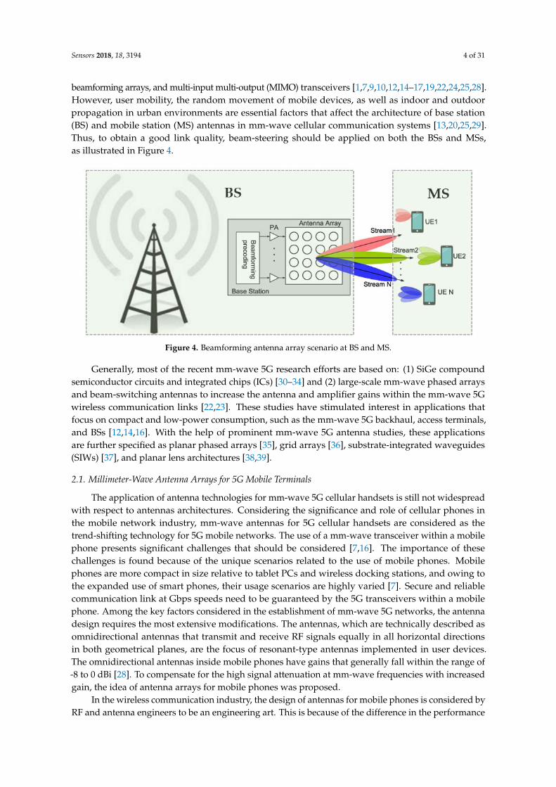
beamforming arrays, and multi-input multi-output (MIMO) transceivers [1,7,9,10,12,14–17,19,22,24,25,28].However, user mobility, the random movement of mobile devices, as well as indoor and outdoorpropagation in urban environments are essential factors that affect the architecture of base station(BS) and mobile station (MS) antennas in mm-wave cellular communication systems [13,20,25,29].Thus, to obtain a good link quality, beam-steering should be applied on both the BSs and MSs,as illustrated in Figure 4.
Sensors 2018, 18, x FOR PEER REVIEW 4 of 33
as phased arrays, beamforming arrays, and multi‐input multi‐output (MIMO) transceivers
[1,7,9,10,12,14–17,19,22,24,25,28]. However, user mobility, the random movement of mobile devices,
as well as indoor and outdoor propagation in urban environments are essential factors that affect the
architecture of base station (BS) and mobile station (MS) antennas in mm‐wave cellular
communication systems [13,20,25,29]. Thus, to obtain a good link quality, beam‐steering should be
applied on both the BSs and MSs, as illustrated in Figure 4.
Figure 4. Beamforming antenna array scenario at BS and MS.
Generally, most of the recent mm‐wave 5G research efforts are based on: (1) SiGe compound
semiconductor circuits and integrated chips (ICs) [30–34] and (2) large‐scale mm‐wave phased arrays
and beam‐switching antennas to increase the antenna and amplifier gains within the mm‐wave 5G
wireless communication links [22,23]. These studies have stimulated interest in applications that
focus on compact and low‐power consumption, such as the mm‐wave 5G backhaul, access terminals,
and BSs [12,14,16]. With the help of prominent mm‐wave 5G antenna studies, these applications are
further specified as planar phased arrays [35], grid arrays [36], substrate‐integrated waveguides
(SIWs) [37], and planar lens architectures [38,39].
2.1. Millimeter‐Wave Antenna Arrays for 5G Mobile Terminals
The application of antenna technologies for mm‐wave 5G cellular handsets is still not
widespread with respect to antennas architectures. Considering the significance and role of cellular
phones in the mobile network industry, mm‐wave antennas for 5G cellular handsets are considered
as the trend‐shifting technology for 5G mobile networks. The use of a mm‐wave transceiver within a
mobile phone presents significant challenges that should be considered [7,16]. The importance of
these challenges is found because of the unique scenarios related to the use of mobile phones. Mobile
phones are more compact in size relative to tablet PCs and wireless docking stations, and owing to
the expanded use of smart phones, their usage scenarios are highly varied [7]. Secure and reliable
communication link at Gbps speeds need to be guaranteed by the 5G transceivers within a mobile
phone. Among the key factors considered in the establishment of mm‐wave 5G networks, the antenna
design requires the most extensive modifications. The antennas, which are technically described as
omnidirectional antennas that transmit and receive RF signals equally in all horizontal directions in
both geometrical planes, are the focus of resonant‐type antennas implemented in user devices. The
omnidirectional antennas inside mobile phones have gains that generally fall within the range of ‐8
to 0 dBi [28]. To compensate for the high signal attenuation at mm‐wave frequencies with increased
gain, the idea of antenna arrays for mobile phones was proposed.
In the wireless communication industry, the design of antennas for mobile phones is considered
by RF and antenna engineers to be an engineering art. This is because of the difference in the
performance of antennas when in an ideal situation in free space and when installed inside a handset.
Figure 4. Beamforming antenna array scenario at BS and MS.
Generally, most of the recent mm-wave 5G research efforts are based on: (1) SiGe compoundsemiconductor circuits and integrated chips (ICs) [30–34] and (2) large-scale mm-wave phased arraysand beam-switching antennas to increase the antenna and amplifier gains within the mm-wave 5Gwireless communication links [22,23]. These studies have stimulated interest in applications thatfocus on compact and low-power consumption, such as the mm-wave 5G backhaul, access terminals,and BSs [12,14,16]. With the help of prominent mm-wave 5G antenna studies, these applicationsare further specified as planar phased arrays [35], grid arrays [36], substrate-integrated waveguides(SIWs) [37], and planar lens architectures [38,39].
2.1. Millimeter-Wave Antenna Arrays for 5G Mobile Terminals
The application of antenna technologies for mm-wave 5G cellular handsets is still not widespreadwith respect to antennas architectures. Considering the significance and role of cellular phones inthe mobile network industry, mm-wave antennas for 5G cellular handsets are considered as thetrend-shifting technology for 5G mobile networks. The use of a mm-wave transceiver within a mobilephone presents significant challenges that should be considered [7,16]. The importance of thesechallenges is found because of the unique scenarios related to the use of mobile phones. Mobilephones are more compact in size relative to tablet PCs and wireless docking stations, and owing tothe expanded use of smart phones, their usage scenarios are highly varied [7]. Secure and reliablecommunication link at Gbps speeds need to be guaranteed by the 5G transceivers within a mobilephone. Among the key factors considered in the establishment of mm-wave 5G networks, the antennadesign requires the most extensive modifications. The antennas, which are technically described asomnidirectional antennas that transmit and receive RF signals equally in all horizontal directionsin both geometrical planes, are the focus of resonant-type antennas implemented in user devices.The omnidirectional antennas inside mobile phones have gains that generally fall within the range of-8 to 0 dBi [28]. To compensate for the high signal attenuation at mm-wave frequencies with increasedgain, the idea of antenna arrays for mobile phones was proposed.
In the wireless communication industry, the design of antennas for mobile phones is considered byRF and antenna engineers to be an engineering art. This is because of the difference in the performance

Sensors 2018, 18, 3194 5 of 31
of antennas when in an ideal situation in free space and when installed inside a handset. It is notpossible for an antenna that is installed in a mobile phone to behave identical to one in free spacewithout considering real-time scenarios. The induced electric and magnet field-coupling due to theantenna surface currents eventually affect the characteristic impedance matching and designed antennaefficiency in free space [16,25,40]. Moreover, the radiation performance of the antenna varies owingto the presence of other electronic components and the metallic casing [41]. Most of the space insidemobile phones is taken up by the large liquid-crystal display (LCD) and battery. The metallic bracketslocated behind the LCD effectively limit the design of current mobile phone antennas to the deviceedges [40]. Moreover, the use of certain metallic frames that are employed for different types ofsensors, cameras, speakers, and microphone modules further reduce the available antenna space insidecellular phones [16]. Therefore, antenna arrays with single- and multilayer printed circuit board (PCB)technologies, polarization diversity, and a wide scanning range will be presented in this paper.
2.1.1. Multilayer Phased-Array Antennas for 5G Mobile Terminals
In [10], Hong et al. presented the basic design concept of mm-wave 5G antennas for cellularphones at 28 GHz. In that study, the design of 1 × 16 mesh-grid antenna-element phased arrays atthe top and bottom positions of cellular phones has been realized using two sets of PCBs, as shownin Figure 5d. The mesh grid antenna elements are arranged in slanted angles of approximately50 at each corner of the PCB. The proposed mesh-grid mm-wave antenna array configurationexhibits a fan-beam radiation characteristic, as shown in Figure 5e. The proposed array antennawas measured in the anechoic chamber at Samsung Electronics headquarters located in Suwon,South Korea. The measurement results show a 130 and 12 3-dB beamwidth in the elevation andazimuth planes, respectively. The proposed array antenna exhibits a 10-dB impedance bandwidth of 1GHz at a 27.9-GHz center frequency. The antenna array inside the cellular device has a measured peakgain of more than 10.5 dBi. The radiation pattern mismatch between the free-space and integratedscenarios is because of diffraction and refraction between the chassis and antenna elements of cellularphones. Figure 5f illustrates the radiation patterns of a mm-wave antenna array in specific beamdirections for both free-space and integrated scenarios. The measurement shows an angular scanningrange of ±70. The proposed antenna array configuration on the top and bottom of the cellular deviceachieved an almost spherical radiation coverage, as shown in Figure 5e.
Sensors 2018, 18, x FOR PEER REVIEW 5 of 33
It is not possible for an antenna that is installed in a mobile phone to behave identical to one in free
space without considering real‐time scenarios. The induced electric and magnet field‐coupling due
to the antenna surface currents eventually affect the characteristic impedance matching and designed
antenna efficiency in free space [16,25,40]. Moreover, the radiation performance of the antenna varies
owing to the presence of other electronic components and the metallic casing [41]. Most of the space
inside mobile phones is taken up by the large liquid‐crystal display (LCD) and battery. The metallic
brackets located behind the LCD effectively limit the design of current mobile phone antennas to the
device edges [40]. Moreover, the use of certain metallic frames that are employed for different types
of sensors, cameras, speakers, and microphone modules further reduce the available antenna space
inside cellular phones [16]. Therefore, antenna arrays with single‐ and multilayer printed circuit
board (PCB) technologies, polarization diversity, and a wide scanning range will be presented in this
paper.
2.1.1. Multilayer Phased‐Array Antennas for 5G Mobile Terminals
In [10], Hong et al. presented the basic design concept of mm‐wave 5G antennas for cellular
phones at 28 GHz. In that study, the design of 1 × 16 mesh‐grid antenna‐element phased arrays at the
top and bottom positions of cellular phones has been realized using two sets of PCBs, as shown in
Figure 5d. The mesh grid antenna elements are arranged in slanted angles of approximately 50° at
each corner of the PCB. The proposed mesh‐grid mm‐wave antenna array configuration exhibits a
fan‐beam radiation characteristic, as shown in Figure 5e. The proposed array antenna was measured
in the anechoic chamber at Samsung Electronics headquarters located in Suwon, South Korea. The
measurement results show a 130° and 12° 3‐dB beamwidth in the elevation and azimuth planes,
respectively. The proposed array antenna exhibits a 10‐dB impedance bandwidth of 1 GHz at a 27.9‐
GHz center frequency. The antenna array inside the cellular device has a measured peak gain of more
than 10.5 dBi. The radiation pattern mismatch between the free‐space and integrated scenarios is
because of diffraction and refraction between the chassis and antenna elements of cellular phones.
Figure 5f illustrates the radiation patterns of a mm‐wave antenna array in specific beam directions
for both free‐space and integrated scenarios. The measurement shows an angular scanning range of
±70°. The proposed antenna array configuration on the top and bottom of the cellular device achieved
an almost spherical radiation coverage, as shown in Figure 5e.
(a)
(b)
(c)
(d)
Figure 5. Cont.

Sensors 2018, 18, 3194 6 of 31Sensors 2018, 18, x FOR PEER REVIEW 6 of 33
(e)
(f)
Figure 5. (a) Comparative illustration of the standard cellular antenna and mm‐wave 5G antenna. (b)
Proposed antenna. (c) Prototype photograph of the standalone mm‐wave antenna array with coaxial
connectors. (d) Photograph of mm‐wave 5G cellular antenna array integrated inside a Samsung
handset and zoomed‐in views of 5G mm‐wave antenna array. (e) mm‐wave antenna array
configuration for 5G cellular mobile terminals. (f) Measured and normalized radiation patterns for
different beam directions (Figure 5f redrawn from [10]).
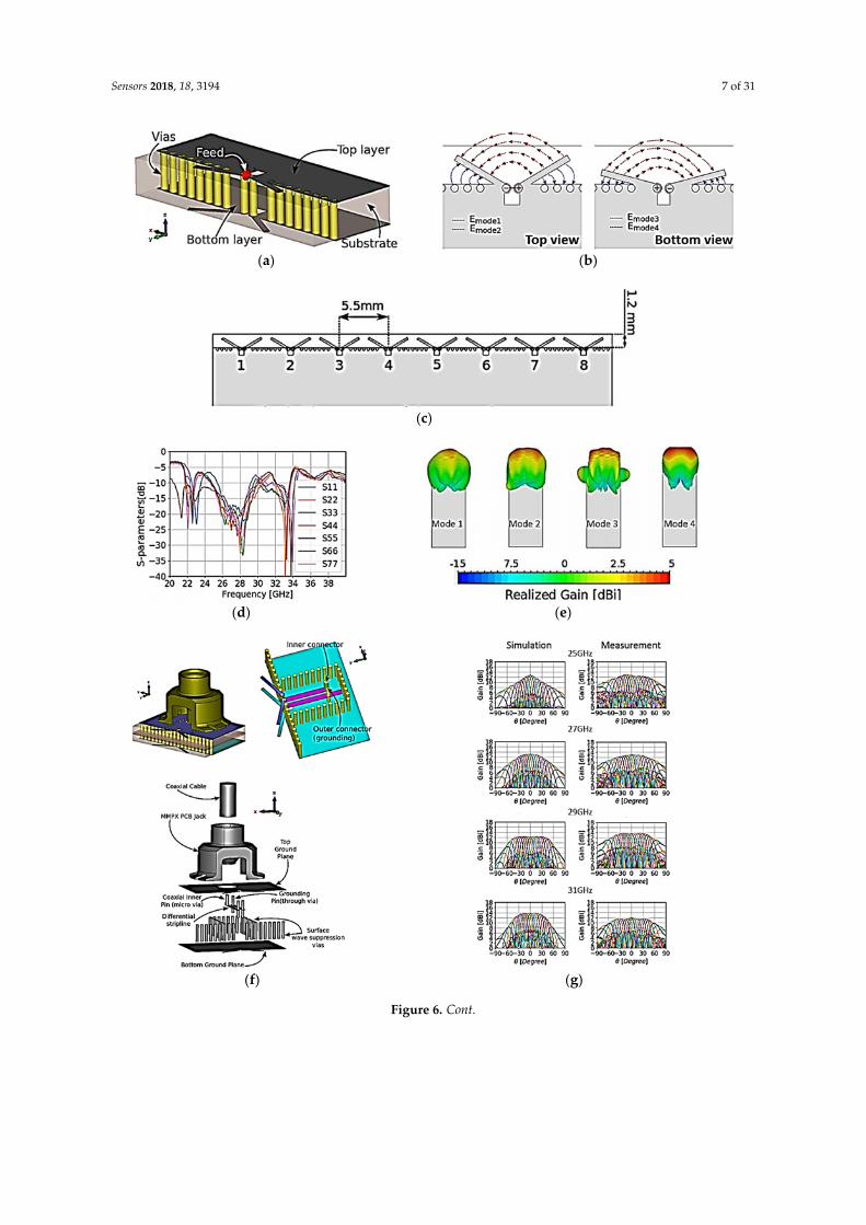
In [42], a planar quad‐mode wideband phased array for a 5G mobile terminal device was
reported. A phased‐array design consists of eight antenna elements with eight MMPX (Micro‐
Miniature Connector) connectors. The proposed phased array is a multilayer design comprising two
Taconic RF‐30 substrate layers with thickness 0.762 mm, having a dielectric constant of 3 and loss
tangent of 0.0014, vias, and microvias. Both layers were glued with FR4 glue having a thickness of 0.2
mm, and a dielectric constant of 4.3 and tangent loss of 0.025. The design overview of the proposed
antenna is shown in Figure 6a. A coaxial‐to‐differential stripline transition feeding is proposed. The
antenna is fed by a differential stripline feed. The top and bottom dipole antennas were connected to
differential stripline through vias, as shown in Figure 6a. The proposed array antenna generates four
distinctive modes when excited, as illustrated in Figure 6b, with an endfire radiation pattern in all
modes. The measured reflection coefficients of the proposed eight‐element phased‐array antenna are
presented in Figure 6d. The main beam‐scanning range is from −90° to +90°. Figure 6g illustrates the
scanning results of the proposed beam‐steering phased‐array antenna at 25, 27, 29, and 31 GHz. The
final prototype of the phased‐array antenna with connectors is shown in Figure 6i.
Figure 5. (a) Comparative illustration of the standard cellular antenna and mm-wave 5G antenna.(b) Proposed antenna. (c) Prototype photograph of the standalone mm-wave antenna array with coaxialconnectors. (d) Photograph of mm-wave 5G cellular antenna array integrated inside a Samsung handsetand zoomed-in views of 5G mm-wave antenna array. (e) mm-wave antenna array configuration for 5Gcellular mobile terminals. (f) Measured and normalized radiation patterns for different beam directions(Figure 5f redrawn from [10]).
In [42], a planar quad-mode wideband phased array for a 5G mobile terminal device wasreported. A phased-array design consists of eight antenna elements with eight MMPX (Micro-MiniatureConnector) connectors. The proposed phased array is a multilayer design comprising two TaconicRF-30 substrate layers with thickness 0.762 mm, having a dielectric constant of 3 and loss tangent of0.0014, vias, and microvias. Both layers were glued with FR4 glue having a thickness of 0.2 mm, and adielectric constant of 4.3 and tangent loss of 0.025. The design overview of the proposed antenna isshown in Figure 6a. A coaxial-to-differential stripline transition feeding is proposed. The antenna isfed by a differential stripline feed. The top and bottom dipole antennas were connected to differentialstripline through vias, as shown in Figure 6a. The proposed array antenna generates four distinctivemodes when excited, as illustrated in Figure 6b, with an endfire radiation pattern in all modes.The measured reflection coefficients of the proposed eight-element phased-array antenna are presentedin Figure 6d. The main beam-scanning range is from −90 to +90. Figure 6g illustrates the scanningresults of the proposed beam-steering phased-array antenna at 25, 27, 29, and 31 GHz. The finalprototype of the phased-array antenna with connectors is shown in Figure 6i.
Sensors 2018, 18, 3194 7 of 31Sensors 2018, 18, x FOR PEER REVIEW 7 of 33
(a)
(b)
(c)
(d)
(e)
(f)
(g)
Figure 6. Cont.

Sensors 2018, 18, 3194 8 of 31Sensors 2018, 18, x FOR PEER REVIEW 8 of 33
(h)
(i)
Figure 6. (a) Three‐dimensional (3D) illustration of proposed antenna element. (b) Electric fields of
proposed antenna’s modes: top view (left) and bottom view (right). (c) Geometry of proposed eight‐
element phased‐array antenna. (d) S‐parameters of proposed phased‐array antenna. (e) 3D radiation
patterns of proposed phased array in all modes. (f) 3D view of antenna and MMPX feeding structure.
(g) Simulated and measured 3D radiation patterns at different scanning angles at 25, 27, 29, and 31
GHz. (h) Overview of the layers in the antenna structure. (i) Prototype of the phased‐array antenna.
(Redrawn from [42])
2.1.2. Multi‐Polarized Multilayer Phased‐Array Antennas for 5G Mobile Terminals
To improve the diversity gain in 5G mobile terminals, the use of multi‐polarized antenna arrays
is a desirable solution to overcome the polarization mismatch problem. A simple demonstration dual‐
polarized mm‐wave antenna with good isolation is reported in [43]. To achieve dual polarizations at
28 GHz, the topology of a side‐by‐side arrangement of horizontal and vertical Yagi‐Uda antennas is
used in [44]. In [45], an aperture antenna array with a dual‐polarized unidirectional pattern through
a back cavity on multilayer PCB technology is proposed.
A multi‐polarized mm‐wave antenna array configuration for 5G mobile terminals was
demonstrated in [46]. The proposed work is the continuation of the previously reported work of
Hong et al. The reported research focuses on losses incurred by the polarization mismatch to enhance
the mm‐wave transmission and reception efficiency. At mm‐wave frequencies, it is complicated to
transmit high‐power energy because of well‐understood propagation and absorption losses. The 5G
wireless communication link budget estimation has become more inflexible owing to real‐life
constraints such as limited battery life. Because mobile antennas integrated inside the mobile
terminals face different angular motions, polarization mismatches between transmit (Tx) and receive
(Rx) antennas have become an important loss factor for mm‐wave cellular communication. To
overcome the polarization mismatch loss factor, two different antenna‐element designs based on the
antenna array schematic are demonstrated and investigated. A coplanar waveguide‐fed horizontally
polarized planar Yagi‐Uda antenna‐element configuration together with a multi‐plate antenna‐
element topology, which excites a vertically polarized electric field, is proposed, as shown in Figure
7a. The 16‐element phased‐array antenna depicted in Figure 7c is designed by deploying the two
linearly polarized antenna elements alternatively along the edge of the mobile terminals with an
angular scanning range of ±80°. By maintaining the distance at less than 3 mm, an isolation of more
than 40 dB was achieved between the horizontally polarized and vertically polarized multi‐antenna
elements. The two sets of 16‐element phased‐array antennas on the opposite corners at the top and
bottom sides of the cellular device provide maximum spherical coverage and polarization diversity.
An antenna array with a maximum height of 0.8 mm was fabricated using 10‐layer FR‐4 lamination.
The dielectric constant and tangent loss at 28 GHz are determined to be 4.2 and 0.09, respectively.
Figure 6. (a) Three-dimensional (3D) illustration of proposed antenna element. (b) Electric fieldsof proposed antenna’s modes: top view (left) and bottom view (right). (c) Geometry of proposedeight-element phased-array antenna. (d) S-parameters of proposed phased-array antenna. (e) 3Dradiation patterns of proposed phased array in all modes. (f) 3D view of antenna and MMPX feedingstructure. (g) Simulated and measured 3D radiation patterns at different scanning angles at 25, 27, 29,and 31 GHz. (h) Overview of the layers in the antenna structure. (i) Prototype of the phased-arrayantenna. (Redrawn from [42])
2.1.2. Multi-Polarized Multilayer Phased-Array Antennas for 5G Mobile Terminals
To improve the diversity gain in 5G mobile terminals, the use of multi-polarized antenna arraysis a desirable solution to overcome the polarization mismatch problem. A simple demonstrationdual-polarized mm-wave antenna with good isolation is reported in [43]. To achieve dual polarizationsat 28 GHz, the topology of a side-by-side arrangement of horizontal and vertical Yagi-Uda antennas isused in [44]. In [45], an aperture antenna array with a dual-polarized unidirectional pattern through aback cavity on multilayer PCB technology is proposed.
A multi-polarized mm-wave antenna array configuration for 5G mobile terminals wasdemonstrated in [46]. The proposed work is the continuation of the previously reported workof Hong et al. The reported research focuses on losses incurred by the polarization mismatchto enhance the mm-wave transmission and reception efficiency. At mm-wave frequencies, it iscomplicated to transmit high-power energy because of well-understood propagation and absorptionlosses. The 5G wireless communication link budget estimation has become more inflexible owingto real-life constraints such as limited battery life. Because mobile antennas integrated inside themobile terminals face different angular motions, polarization mismatches between transmit (Tx) andreceive (Rx) antennas have become an important loss factor for mm-wave cellular communication.To overcome the polarization mismatch loss factor, two different antenna-element designs basedon the antenna array schematic are demonstrated and investigated. A coplanar waveguide-fedhorizontally polarized planar Yagi-Uda antenna-element configuration together with a multi-plateantenna-element topology, which excites a vertically polarized electric field, is proposed, as shown inFigure 7a. The 16-element phased-array antenna depicted in Figure 7c is designed by deploying thetwo linearly polarized antenna elements alternatively along the edge of the mobile terminals with anangular scanning range of ±80. By maintaining the distance at less than 3 mm, an isolation of morethan 40 dB was achieved between the horizontally polarized and vertically polarized multi-antennaelements. The two sets of 16-element phased-array antennas on the opposite corners at the top andbottom sides of the cellular device provide maximum spherical coverage and polarization diversity.An antenna array with a maximum height of 0.8 mm was fabricated using 10-layer FR-4 lamination.The dielectric constant and tangent loss at 28 GHz are determined to be 4.2 and 0.09, respectively.

Sensors 2018, 18, 3194 9 of 31Sensors 2018, 18, x FOR PEER REVIEW 9 of 33
(a)
(b)
(c)
(d)
Figure 7. (a) Two discrete 28‐GHz mm‐wave antenna elements, i.e., the horizontally polarized planar
Yagi‐Uda antenna (left), and the vertically polarized multi‐plate antenna (right). (b) Final topology of
vertically polarized multi‐plate antenna. (c) 16‐element phased‐array configuration at the edge of the
mobile terminal. (d) Photograph of the prototype testing in an anechoic chamber and close‐up view
of 5G mm‐wave phased‐array antenna (Redrawn from [46]).
A multi‐polarized antenna array that integrates the horizontally and vertically polarized quasi‐
Yagi antennas together into a single area was implemented and demonstrated in [47] for 5G mobile
terminals, achieving polarization diversity and size reductions. To achieve polarization diversity
along with the beam‐scanning capability, dual‐polarized quasi‐Yagi‐Uda antennas for both the
corner edges and a lateral array design were addressed, as illustrated in Figure 8a. The proposed
array antenna was implemented on a three‐layer structure on a Rogers4003 substrate with a total
thickness of 1.93 mm, which has a dielectric constant of 3.38 and a tangent loss of 0.0027. The
implemented horizontally polarized and vertically polarized antenna array designs for the lateral
edge as well as the multi‐polarized antenna for the corner edges are shown in Figure 8b. The 10‐dB
Figure 7. (a) Two discrete 28-GHz mm-wave antenna elements, i.e., the horizontally polarized planarYagi-Uda antenna (left), and the vertically polarized multi-plate antenna (right). (b) Final topology ofvertically polarized multi-plate antenna. (c) 16-element phased-array configuration at the edge of themobile terminal. (d) Photograph of the prototype testing in an anechoic chamber and close-up view of5G mm-wave phased-array antenna (Redrawn from [46]).
A multi-polarized antenna array that integrates the horizontally and vertically polarizedquasi-Yagi antennas together into a single area was implemented and demonstrated in [47] for5G mobile terminals, achieving polarization diversity and size reductions. To achieve polarizationdiversity along with the beam-scanning capability, dual-polarized quasi-Yagi-Uda antennas for both thecorner edges and a lateral array design were addressed, as illustrated in Figure 8a. The proposed arrayantenna was implemented on a three-layer structure on a Rogers4003 substrate with a total thicknessof 1.93 mm, which has a dielectric constant of 3.38 and a tangent loss of 0.0027. The implemented
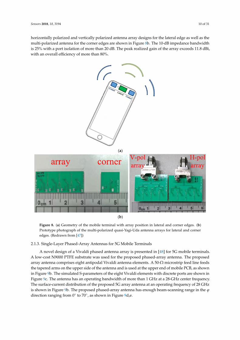
Sensors 2018, 18, 3194 10 of 31
horizontally polarized and vertically polarized antenna array designs for the lateral edge as well as themulti-polarized antenna for the corner edges are shown in Figure 8b. The 10-dB impedance bandwidthis 25% with a port isolation of more than 20 dB. The peak realized gain of the array exceeds 11.8 dBi,with an overall efficiency of more than 80%.
Sensors 2018, 18, x FOR PEER REVIEW 10 of 33
impedance bandwidth is 25% with a port isolation of more than 20 dB. The peak realized gain of the
array exceeds 11.8 dBi, with an overall efficiency of more than 80%.
(a)
(b)
Figure 8. (a) Geometry of the mobile terminal with array position in lateral and corner edges. (b)
Prototype photograph of the multi‐polarized quasi‐Yagi‐Uda antenna arrays for lateral and corner
edges. (Redrawn from [47])
2.1.3. Single‐Layer Phased‐Array Antennas for 5G Mobile Terminals
A novel design of a Vivaldi phased antenna array is presented in [48] for 5G mobile terminals.
A low‐cost N9000 PTFE substrate was used for the proposed phased‐array antenna. The proposed
array antenna comprises eight antipodal Vivaldi antenna elements. A 50‐Ω microstrip feed line feeds
the tapered arms on the upper side of the antenna and is used at the upper end of mobile PCB, as
shown in Figure 9b. The simulated S‐parameters of the eight Vivaldi elements with discrete ports are
shown in Figure 9c. The antenna has an operating bandwidth of more than 1 GHz at a 28‐GHz center
frequency. The surface‐current distribution of the proposed 5G array antenna at an operating
frequency of 28 GHz is shown in Figure 9b. The proposed phased‐array antenna has enough beam‐
scanning range in the φ direction ranging from 0° to 70°, as shown in Figure 9d,e.
Figure 8. (a) Geometry of the mobile terminal with array position in lateral and corner edges. (b)Prototype photograph of the multi-polarized quasi-Yagi-Uda antenna arrays for lateral and corneredges. (Redrawn from [47])
2.1.3. Single-Layer Phased-Array Antennas for 5G Mobile Terminals
A novel design of a Vivaldi phased antenna array is presented in [48] for 5G mobile terminals.A low-cost N9000 PTFE substrate was used for the proposed phased-array antenna. The proposedarray antenna comprises eight antipodal Vivaldi antenna elements. A 50-Ω microstrip feed line feedsthe tapered arms on the upper side of the antenna and is used at the upper end of mobile PCB, as shownin Figure 9b. The simulated S-parameters of the eight Vivaldi elements with discrete ports are shown inFigure 9c. The antenna has an operating bandwidth of more than 1 GHz at a 28-GHz center frequency.The surface-current distribution of the proposed 5G array antenna at an operating frequency of 28 GHzis shown in Figure 9b. The proposed phased-array antenna has enough beam-scanning range in the ϕ
direction ranging from 0 to 70, as shown in Figure 9d,e.

Sensors 2018, 18, 3194 11 of 31Sensors 2018, 18, x FOR PEER REVIEW 11 of 33
(a)
(b)
(c)
(d)
(e)
Figure 9. (a) Geometry of the Vivaldi phased‐array antenna. (b) Surface‐current distribution of
proposed phased‐array antenna at 28 GHz. (c) Simulated S‐parameters of the proposed Vivaldi
antenna array elements. (d) Radiation patterns of the antenna at different scanning angles. (e)
Realized gain patterns of the antenna at different scanning angles. (Redrawn from [48]).
A phased‐array antenna with switchable three‐dimensional (3D) scanning for 5G mobile
terminals was proposed in [49]. Three similar subarrays of patch antennas arranged along the edge
of the mobile terminal were proposed. Each subarray consists of eight microstrip patch antenna
elements (MPAs) and has a beam‐scanning capability of ±90° in the θ plane. The antenna was
designed on the Nelco N9000 substrate having a thickness of 0.787 mm with a dielectric constant of
2.2 and tangent loss of 0.0009. Figure 10c illustrates an architecture to implement feeding using low‐
loss phase shifters with a 4.5‐dB insertion loss for beam‐steering, and a microwave SP3T switch to
switch between the subarrays. The proposed design has a 1‐GHz 10‐dB impedance bandwidth in the
Figure 9. (a) Geometry of the Vivaldi phased-array antenna. (b) Surface-current distribution ofproposed phased-array antenna at 28 GHz. (c) Simulated S-parameters of the proposed Vivaldi antennaarray elements. (d) Radiation patterns of the antenna at different scanning angles. (e) Realized gainpatterns of the antenna at different scanning angles. (Redrawn from [48]).
A phased-array antenna with switchable three-dimensional (3D) scanning for 5G mobile terminalswas proposed in [49]. Three similar subarrays of patch antennas arranged along the edge of the mobileterminal were proposed. Each subarray consists of eight microstrip patch antenna elements (MPAs)and has a beam-scanning capability of ±90 in the θ plane. The antenna was designed on the NelcoN9000 substrate having a thickness of 0.787 mm with a dielectric constant of 2.2 and tangent loss of0.0009. Figure 10c illustrates an architecture to implement feeding using low-loss phase shifters with a

Sensors 2018, 18, 3194 12 of 31
4.5-dB insertion loss for beam-steering, and a microwave SP3T switch to switch between the subarrays.The proposed design has a 1-GHz 10-dB impedance bandwidth in the frequency range from 21 to22 GHz, as shown in Figure 10b. The proposed phased-array design has a good beam-scanning rangeof −90 to +90 with a gain of more than 12.5 dBi, as shown in Figure 10d,e.
Sensors 2018, 18, x FOR PEER REVIEW 12 of 33
frequency range from 21 to 22 GHz, as shown in Figure 10b. The proposed phased‐array design has
a good beam‐scanning range of −90° to +90° with a gain of more than 12.5 dBi, as shown in Figure
10d,e.
(a)
(b)
(c)
(d)
(e)
Figure 10. (a) Proposed view of 5G phased‐array antenna with full ground plane. (b) S‐parameters of
proposed phased‐array antenna with eight elements. (c) Proposed phased‐array architecture. (d) 3D
radiation patterns of each subarray at different scan angles. (e) 2D realized gain patterns at different
scan angles. (Redrawn from [49])
The 3D beam coverage was achieved and proposed by Zhang et al. in [50]. Three planar phased
subarray configurations, as shown in Figure 11b, were used to change/switch the beam pattern to
Figure 10. (a) Proposed view of 5G phased-array antenna with full ground plane. (b) S-parameters ofproposed phased-array antenna with eight elements. (c) Proposed phased-array architecture. (d) 3Dradiation patterns of each subarray at different scan angles. (e) 2D realized gain patterns at differentscan angles. (Redrawn from [49])

Sensors 2018, 18, 3194 13 of 31
The 3D beam coverage was achieved and proposed by Zhang et al. in [50]. Three planar phasedsubarray configurations, as shown in Figure 11b, were used to change/switch the beam pattern to theirdistinct regions using chassis surface-wave excitation. The 3D spherical coverage is achieved by mergingthe beam patterns of subarrays. The proposed antenna has a 2-GHz 10-dB impedance bandwidth at28 GHz, as shown in Figure 11b. A Nelco N9000 PCB substrate was used to design the antenna with adielectric constant of 2.2 and a loss tangent of 0.0009. The substrate dimensions are 65 mm × 130 mm,with a thickness of 0.764 mm. A subarray comprises eight slot elements, each with a dimension of4.85 mm × 0.5 mm. The consecutive slot-element distance from center-to-center is 5.35 mm. The wholephased-array switches the main beam between subarrays in the ϕ direction, and scans the beam in theθ direction with variable phase shifts, as shown in Figure 11c,d. All the elements between subarraysA, B and B, C have a mutual coupling lower than −12.3 dB and −9.4 dB, respectively. The angularscanning range of subarrays A, B, and C point in the ϕ directions of ±73, ±128, and ±20, respectively.The efficiency of subarrays A, B, and C are 74.3%, 68%, and 72.2%, respectively.
Sensors 2018, 18, x FOR PEER REVIEW 13 of 33
their distinct regions using chassis surface‐wave excitation. The 3D spherical coverage is achieved by
merging the beam patterns of subarrays. The proposed antenna has a 2‐GHz 10‐dB impedance
bandwidth at 28 GHz, as shown in Figure 11b. A Nelco N9000 PCB substrate was used to design the
antenna with a dielectric constant of 2.2 and a loss tangent of 0.0009. The substrate dimensions are 65
mm × 130 mm, with a thickness of 0.764 mm. A subarray comprises eight slot elements, each with a
dimension of 4.85 mm × 0.5 mm. The consecutive slot‐element distance from center‐to‐center is 5.35
mm. The whole phased‐array switches the main beam between subarrays in the φ direction, and
scans the beam in the θ direction with variable phase shifts, as shown in Figure 11c,d. All the elements
between subarrays A, B and B, C have a mutual coupling lower than −12.3 dB and −9.4 dB,
respectively. The angular scanning range of subarrays A, B, and C point in the φ directions of ±73°,
±128°, and ±20°, respectively. The efficiency of subarrays A, B, and C are 74.3%, 68%, and 72.2%,
respectively.
(a)
(b)
(c)
(d)
(e)
(f)
Figure 11. (a) Printed switchable array antenna configuration of subarrays. (b) S‐parameter plots of
proposed array antenna for elements 4, 12, and 20 in subarrays A, B, and C, respectively, using
discrete ports. (c) Gain patterns with beam‐steering in the φ direction of each subarray with all
elements. (d) Radiation gain patterns with 70° beam‐scanning: at φ = 73° for subarray A, at φ = 128°
for subarray B, at φ = 20° for subarray C. (e) Illustration of proposed phased‐array antenna with
coaxial feed cables. (f) Prototype of proposed phased‐array antenna with coaxial feed cables.
(Redrawn from [50])
Figure 11. (a) Printed switchable array antenna configuration of subarrays. (b) S-parameter plots ofproposed array antenna for elements 4, 12, and 20 in subarrays A, B, and C, respectively, using discreteports. (c) Gain patterns with beam-steering in the ϕ direction of each subarray with all elements.(d) Radiation gain patterns with 70 beam-scanning: at ϕ = 73 for subarray A, at ϕ = 128 for subarrayB, at ϕ = 20 for subarray C. (e) Illustration of proposed phased-array antenna with coaxial feed cables.(f) Prototype of proposed phased-array antenna with coaxial feed cables. (Redrawn from [50])

Sensors 2018, 18, 3194 14 of 31
Zhang et al. also reported a study of user effects on the proposed switchable array in user mode,i.e., talking mode and data mode, at 28 GHz. Figure 12a illustrates different setups in user mode,where ‘’top” and ‘’bottom” indicate the switchable array position at the top of the chassis near tothe index finger and at the bottom of the chassis close to the hand palm, respectively. The electricalproperties of skin and different tissues were taken from [50]. Parametric results for the switchable arrayon the top and bottom of the chassis in talking mode and data usage mode are shown in Figure 12b,c,respectively. Based on the parametric analysis and results, it is proposed that the switchable arrayhas a better performance in terms of beam-switching, body loss, and realized gain on the chassis topposition when compared with the bottom of the chassis. It is also proposed to design an additionalarray on the bottom side of the chassis, which results in a decreased shadowing effect in talking mode.
Sensors 2018, 18, x FOR PEER REVIEW 14 of 33
Zhang et al. also reported a study of user effects on the proposed switchable array in user mode,
i.e., talking mode and data mode, at 28 GHz. Figure 12a illustrates different setups in user mode,
where ‘’top” and ‘’bottom” indicate the switchable array position at the top of the chassis near to the
index finger and at the bottom of the chassis close to the hand palm, respectively. The electrical
properties of skin and different tissues were taken from [50]. Parametric results for the switchable
array on the top and bottom of the chassis in talking mode and data usage mode are shown in Figure
12b,c, respectively. Based on the parametric analysis and results, it is proposed that the switchable
array has a better performance in terms of beam‐switching, body loss, and realized gain on the chassis
top position when compared with the bottom of the chassis. It is also proposed to design an additional
array on the bottom side of the chassis, which results in a decreased shadowing effect in talking mode.
(a)
(b)
(c)
(d)
Figure 12. (a) User effect setup for: talk mode (left) and data mode (right). (b) Gain plots of each
subarray for top and bottom sides of chassis in talking mode. (c) Gain plots of each subarray for top
and bottom sides of chassis in data usage mode. (d) Measurement setup for free space (left) and for
talking mode with real person (right). (Redrawn from [50])
Figure 12. (a) User effect setup for: talk mode (left) and data mode (right). (b) Gain plots of eachsubarray for top and bottom sides of chassis in talking mode. (c) Gain plots of each subarray for topand bottom sides of chassis in data usage mode. (d) Measurement setup for free space (left) and fortalking mode with real person (right). (Redrawn from [50])

Sensors 2018, 18, 3194 15 of 31
Yu et al. presented a study and design of a novel phased-array antenna operating at 28 GHzwith beam-steering applications for a 5G mobile terminal with metallic casing in [41]. The proposedbeam-steering array comprises two subarrays, each having eight identical elements on both sides ofa mobile device with a metallic casing, as shown in Figure 13a. A slot element with a cavity-backedstructure is proposed, which is easy to fabricate on the metallic casing of the mobile terminal.An important factor is to determine the optimum position of the proposed phased subarrays insidethe mobile terminal before finalizing the actual design in practice. The length of the slot is kept at thehalf-guided wavelength λg/2, i.e., 5.8 mm at an operating frequency of 28 GHz, and the correspondingslot width is 1.5 mm with a cavity height of 4 mm. The high-gain directional radiation pattern ofthe slot element is achieved. Figure 13c illustrates the design of one of the proposed eight-elementphased arrays. It is proposed to use small stepped pins soldered on the microstrip feed line feedingeach element of the subarray. The microstrip feeding line is printed on a 0.254-mm-thick Rogers5880 substrate having a dielectric constant of 2.2 and a loss tangent/of 0.0009. Each element has beenprovided by the phase variation using 6-bit phase shifters within a 28-GHz front-end RF integratedcircuit (RFIC) chip to accomplish beam-steering, as illustrated in Figure 13e. Figure 13d shows theblock diagram of the eight-element beam-steering phased array.
Sensors 2018, 18, x FOR PEER REVIEW 15 of 33
Yu et al. presented a study and design of a novel phased‐array antenna operating at 28 GHz with
beam‐steering applications for a 5G mobile terminal with metallic casing in [41]. The proposed beam‐
steering array comprises two subarrays, each having eight identical elements on both sides of a
mobile device with a metallic casing, as shown in Figure 13a. A slot element with a cavity‐backed
structure is proposed, which is easy to fabricate on the metallic casing of the mobile terminal. An
important factor is to determine the optimum position of the proposed phased subarrays inside the
mobile terminal before finalizing the actual design in practice. The length of the slot is kept at the
half‐guided wavelength λg/2, i.e., 5.8 mm at an operating frequency of 28 GHz, and the corresponding
slot width is 1.5 mm with a cavity height of 4 mm. The high‐gain directional radiation pattern of the
slot element is achieved. Figure 13c illustrates the design of one of the proposed eight‐element phased
arrays. It is proposed to use small stepped pins soldered on the microstrip feed line feeding each
element of the subarray. The microstrip feeding line is printed on a 0.254‐mm‐thick Rogers 5880
substrate having a dielectric constant of 2.2 and a loss tangent/of 0.0009. Each element has been
provided by the phase variation using 6‐bit phase shifters within a 28‐GHz front‐end RF integrated
circuit (RFIC) chip to accomplish beam‐steering, as illustrated in Figure 13e. Figure 13d shows the
block diagram of the eight‐element beam‐steering phased array.
(a)
(b)
(c)
(d)
(e)
Figure 13. Cont.

Sensors 2018, 18, 3194 16 of 31Sensors 2018, 18, x FOR PEER REVIEW 16 of 33
(f)
(g)
Figure 13. (a) Different views of mobile terminal design. (b) Photograph of mobile terminal with
proposed phased‐array antennas. (c) Design of proposed eight‐element antenna array. (d) Block
diagram of eight‐element beam‐steering antenna array. (e) Block diagram description of 28‐GHz
front‐end RFIC chip. (f) Simulated and measured input reflection coefficients and isolation between
array elements. (g) 2D radiation plots at different scanning angles (Redrawn from [41]).
Figure 13f shows the simulated and experimented S11 and S21 plots. The proposed beam‐steering
phased‐array has achieved an angular scanning range of 0° to 60° at 28 GHz, as shown in Figure 13g.
The gain variation in the angular scanning range of ±60° is symmetrical with 15.6 dBi as peak gain.
Two‐dimensional (2D) radiation plots for various scanning angles of the proposed phased array are
shown in Figure 13g.
Yu et al. also presented the effect of the user’s body on the gain and impedance matching of the
proposed phased array, as illustrated in Figure 14a,b. The analysis of the user’s body effects on the
proposed 16‐element phased arrays shows that it can achieve a reasonable gain of at least 6.9 dBi,
even with the user’s body effects.
(a)
(b)
Figure 14. (a) Effects of user’s body on the proposed eight‐element phased array with different beam‐
scanning angles positioned on the left side of mobile terminal. (b) User body effects on the eight‐
element phased array located along the right edge of mobile terminal at different beam‐scanning
angles. (Redrawn from [41])
Figure 13. (a) Different views of mobile terminal design. (b) Photograph of mobile terminal withproposed phased-array antennas. (c) Design of proposed eight-element antenna array. (d) Blockdiagram of eight-element beam-steering antenna array. (e) Block diagram description of 28-GHzfront-end RFIC chip. (f) Simulated and measured input reflection coefficients and isolation betweenarray elements. (g) 2D radiation plots at different scanning angles (Redrawn from [41]).
Figure 13f shows the simulated and experimented S11 and S21 plots. The proposed beam-steeringphased-array has achieved an angular scanning range of 0 to 60 at 28 GHz, as shown in Figure 13g.The gain variation in the angular scanning range of ±60 is symmetrical with 15.6 dBi as peak gain.Two-dimensional (2D) radiation plots for various scanning angles of the proposed phased array areshown in Figure 13g.
Yu et al. also presented the effect of the user’s body on the gain and impedance matching of theproposed phased array, as illustrated in Figure 14a,b. The analysis of the user’s body effects on theproposed 16-element phased arrays shows that it can achieve a reasonable gain of at least 6.9 dBi,even with the user’s body effects.
Sensors 2018, 18, x FOR PEER REVIEW 16 of 33
(f)
(g)
Figure 13. (a) Different views of mobile terminal design. (b) Photograph of mobile terminal with
proposed phased‐array antennas. (c) Design of proposed eight‐element antenna array. (d) Block
diagram of eight‐element beam‐steering antenna array. (e) Block diagram description of 28‐GHz
front‐end RFIC chip. (f) Simulated and measured input reflection coefficients and isolation between
array elements. (g) 2D radiation plots at different scanning angles (Redrawn from [41]).
Figure 13f shows the simulated and experimented S11 and S21 plots. The proposed beam‐steering
phased‐array has achieved an angular scanning range of 0° to 60° at 28 GHz, as shown in Figure 13g.
The gain variation in the angular scanning range of ±60° is symmetrical with 15.6 dBi as peak gain.
Two‐dimensional (2D) radiation plots for various scanning angles of the proposed phased array are
shown in Figure 13g.
Yu et al. also presented the effect of the user’s body on the gain and impedance matching of the
proposed phased array, as illustrated in Figure 14a,b. The analysis of the user’s body effects on the
proposed 16‐element phased arrays shows that it can achieve a reasonable gain of at least 6.9 dBi,
even with the user’s body effects.
(a)
(b)
Figure 14. (a) Effects of user’s body on the proposed eight‐element phased array with different beam‐
scanning angles positioned on the left side of mobile terminal. (b) User body effects on the eight‐
element phased array located along the right edge of mobile terminal at different beam‐scanning
angles. (Redrawn from [41])
Figure 14. (a) Effects of user’s body on the proposed eight-element phased array with differentbeam-scanning angles positioned on the left side of mobile terminal. (b) User body effects on theeight-element phased array located along the right edge of mobile terminal at different beam-scanningangles. (Redrawn from [41])
Table 1 categorizes the performance of recent phased arrays for the 5G mobile terminal devicesdiscussed in this section. A performance comparison has been made based on the beam-scanningcapability, peak gain, and array elements of various phased arrays.

Sensors 2018, 18, 3194 17 of 31
Table 1. Performance variation of various phased arrays for 5G mobile terminals.
Ref # No. of Subarrays Elements Per Subarray fo (GHz) BW (GHz) Beam-Scanning (deg) Peak Gain (dBi) Substrate Array Position
[10] 2 1 × 16 27.9 =1 ±70 10.5 Multilayer-PCB Top and Bottom[46] 4 1 × 16 28 - ±80 - Multilayer-FR4 Four Corners[49] 3 1 × 8 21.5 =1 ±90 12.5 Nelco N9000 Top[48] 1 1 × 8 28 >1 ±70 12 N900 PTFE Top[50] 3 1 × 8 28 =2 ±73, ±128, ±20 12.5 Nelco N9000 Top[41] 2 1 × 8 28 >2.5 ±60 15.6 Metallic casing Left and Right[42] 1 1 × 8 28 >8 ±90 12 Taconic RF-30 Top[47] 3 1, 1 × 4, 1 36 >2 - 11 Multilayer-PCB Top (Mid + Corners)

Sensors 2018, 18, 3194 18 of 31
2.2. Millimeter-Wave Phased Arrays for 5G Access Terminals
In mm-wave cellular networks, backhaul systems and BSs will generally be deployed in crowdyenvironment on the poles, beacons, and building tops. The combined data to or from the multiple userswill be transmitted with less delay from the mm-wave BS to the central hub through various mm-wavewireless or optical channels. The communication range for the outdoor mm-wave access link wouldbe larger when compared to indoor mm-wave communication links, but the power consumptionof the user end terminals cannot be increased. Because of the high signal attenuation at mm-wavefrequencies, the effective communication distance of mm-wave systems is limited when compared tomicrowave signals. To reduce the increased path loss in outdoor environments, and owing to the usermobility, a suitable beamforming technique is required for implementation in cellular communicationaccess links in the mm-wave frequency band. This can be realized by using the mm-wave BS equippedwith high-gain phased arrays, where there is a relaxation of size and power consumption requirements.Phased arrays at millimeter-wave frequencies present a high-data-rate communication solution usinghigh bandwidth and directional links between the BS and MS terminals.
2.2.1. Millimeter-Wave PCB Phased Arrays
In [9], Zhang et al. presented a comparative analysis of different antenna array architecturesand beamforming techniques for outdoor mm-wave communication systems. Four different types ofarray architectures, i.e., an 8 × 8 rectangular element array, 64 circular element array, 61 hexagonalelement array, and 16 cross-shaped element array architectures were analyzed, as depicted in Figure 15.The 2D radiation plots that were retrieved from 3D radiation patterns are illustrated in Figure 15.The analysis of different array architectures shows that the array architecture with circular elementshas a larger coverage area with high gain and directivity compared to those of the other antennaarray architectures.
Sensors 2018, 18, x FOR PEER REVIEW 19 of 33
2.2. Millimeter‐Wave Phased Arrays for 5G Access Terminals
In mm‐wave cellular networks, backhaul systems and BSs will generally be deployed in crowdy
environment on the poles, beacons, and building tops. The combined data to or from the multiple
users will be transmitted with less delay from the mm‐wave BS to the central hub through various
mm‐wave wireless or optical channels. The communication range for the outdoor mm‐wave access
link would be larger when compared to indoor mm‐wave communication links, but the power
consumption of the user end terminals cannot be increased. Because of the high signal attenuation at
mm‐wave frequencies, the effective communication distance of mm‐wave systems is limited when
compared to microwave signals. To reduce the increased path loss in outdoor environments, and
owing to the user mobility, a suitable beamforming technique is required for implementation in
cellular communication access links in the mm‐wave frequency band. This can be realized by using
the mm‐wave BS equipped with high‐gain phased arrays, where there is a relaxation of size and
power consumption requirements. Phased arrays at millimeter‐wave frequencies present a high‐
data‐rate communication solution using high bandwidth and directional links between the BS and
MS terminals.
2.2.1. Millimeter‐Wave PCB Phased Arrays
In [9], Zhang et al. presented a comparative analysis of different antenna array architectures and
beamforming techniques for outdoor mm‐wave communication systems. Four different types of
array architectures, i.e., an 8 × 8 rectangular element array, 64 circular element array, 61 hexagonal
element array, and 16 cross‐shaped element array architectures were analyzed, as depicted in Figure
15. The 2D radiation plots that were retrieved from 3D radiation patterns are illustrated in Figure 15.
The analysis of different array architectures shows that the array architecture with circular elements
has a larger coverage area with high gain and directivity compared to those of the other antenna
array architectures.
(a)
(b)
(c)
(d)
Figure 15. 2D radiation plots of (a) 8 × 8 rectangular element array, (b) 16 cross‐shaped element array,
(c) 64 circular element array, and (d) 61 hexagonal element array (Redrawn from [9]).
Figure 15. 2D radiation plots of (a) 8 × 8 rectangular element array, (b) 16 cross-shaped element array,(c) 64 circular element array, and (d) 61 hexagonal element array (Redrawn from [9]).

Sensors 2018, 18, 3194 19 of 31
In [13], a testbed with a bandwidth of 800 MHz at an operating frequency of 28 GHz, which wasbuilt to test the practicality of mm-wave cellular communications at Samsung Electronics, (Suwon)Korea, was presented. The BS antenna array consisted of (6 × 8) 48 antenna elements that are groupedas subarrays in groups of three antenna elements to reduce the complexity of the system components.Each subarray provides a horizontal beam-scanning of 110 with the aid of a connected phase shifter,mixer, and an RF path. The MS antenna array was composed of two antenna subarrays, where eachsubarray provides horizontal beam-scanning of either 90 or 180, with four elements designed onone of the sides of the RF board. The design overview of the BS and MS antenna arrays are shown inFigure 16a,b, respectively.
Sensors 2018, 18, x FOR PEER REVIEW 20 of 33
In [13], a testbed with a bandwidth of 800 MHz at an operating frequency of 28 GHz, which was
built to test the practicality of mm‐wave cellular communications at Samsung Electronics, (Suwon)
Korea, was presented. The BS antenna array consisted of (6 × 8) 48 antenna elements that are grouped
as subarrays in groups of three antenna elements to reduce the complexity of the system components.
Each subarray provides a horizontal beam‐scanning of 110° with the aid of a connected phase shifter,
mixer, and an RF path. The MS antenna array was composed of two antenna subarrays, where each
subarray provides horizontal beam‐scanning of either 90° or 180°, with four elements designed on
one of the sides of the RF board. The design overview of the BS and MS antenna arrays are shown in
Figure 16a,b, respectively.
(a)
(b)
(c)
(d)
Figure 16. (a) Transceiver array antenna for BS. (b) Transceiver array antenna for MS. (c) Block
diagram of testbed for mm‐wave cellular communication with beamforming antenna array. (d)
Testbed structure built at Samsung Electronics, Korea. (Redrawn from [13])
In [39], Jiang et al. proposed a novel array architecture for beamforming and multibeam massive
MIMO systems using a metamaterial‐based thin planar lens antenna. The proposed antenna
comprises an EM lens combined with an antenna array. The EM lens together with an antenna array
helps to increase the throughput and data rate of massive MIMO (m‐MIMO). Both the lens and
antenna elements were fabricated using PCB technology. Figure 17a,b respectively presents the side
and top views of the proposed lens antenna. An array of a seven‐element SIW‐fed stacked patch
antenna operating at 28 GHz is placed at the focal region behind the EM lens. Each subarray
comprises four SIW‐fed square patches as radiating patches. Each array element is connected to the
input port using SIW‐to‐grounded‐coplanar‐waveguide (GCPW) transition feeding. The design
overview of the seven‐element SIW‐fed stacked patch antenna array is given in Figure 17b. The
proposed multilayer antenna array is fabricated on a Rogers RO4003C substrate having a dielectric
constant of 3.55 and loss tangent of 0.0027. The thickness of the top and bottom layers is 0.508 mm
and 0.813 mm, respectively. Both layers are joined together with a bonding layer of Rogers RO4450B,
Figure 16. (a) Transceiver array antenna for BS. (b) Transceiver array antenna for MS. (c) Block diagramof testbed for mm-wave cellular communication with beamforming antenna array. (d) Testbed structurebuilt at Samsung Electronics, Korea. (Redrawn from [13])
In [39], Jiang et al. proposed a novel array architecture for beamforming and multibeam massiveMIMO systems using a metamaterial-based thin planar lens antenna. The proposed antenna comprisesan EM lens combined with an antenna array. The EM lens together with an antenna array helpsto increase the throughput and data rate of massive MIMO (m-MIMO). Both the lens and antennaelements were fabricated using PCB technology. Figure 17a,b respectively presents the side and topviews of the proposed lens antenna. An array of a seven-element SIW-fed stacked patch antennaoperating at 28 GHz is placed at the focal region behind the EM lens. Each subarray comprisesfour SIW-fed square patches as radiating patches. Each array element is connected to the input portusing SIW-to-grounded-coplanar-waveguide (GCPW) transition feeding. The design overview of theseven-element SIW-fed stacked patch antenna array is given in Figure 17b. The proposed multilayerantenna array is fabricated on a Rogers RO4003C substrate having a dielectric constant of 3.55 and losstangent of 0.0027. The thickness of the top and bottom layers is 0.508 mm and 0.813 mm, respectively.

Sensors 2018, 18, 3194 20 of 31
Both layers are joined together with a bonding layer of Rogers RO4450B, which has a dielectric constantof 3.54, loss tangent of 0.004, and height of 0.202 mm. A photograph of the fabricated prototype of theproposed seven-element array loaded with an EM lens is shown in Figure 17c. The measured 10-dBimpedance matching ranges from 25.8–28.9 GHz, as shown in Figure 17d. The angular beam-scanningrange of the proposed phased array is from −27 to +27. Figure 17e shows the experimented radiationpatterns of the proposed phased-array lens integrated antenna at 28 GHz. The measured peak gain ofthe lens-fed phased-array antenna is 24.2 dBi, with an efficiency of 24.5% at a frequency of 27.5 GHz.
Sensors 2018, 18, x FOR PEER REVIEW 21 of 33
which has a dielectric constant of 3.54, loss tangent of 0.004, and height of 0.202 mm. A photograph
of the fabricated prototype of the proposed seven‐element array loaded with an EM lens is shown in
Figure 17c. The measured 10‐dB impedance matching ranges from 25.8–28.9 GHz, as shown in Figure
17d. The angular beam‐scanning range of the proposed phased array is from −27° to +27°. Figure 17e
shows the experimented radiation patterns of the proposed phased‐array lens integrated antenna at
28 GHz. The measured peak gain of the lens‐fed phased‐array antenna is 24.2 dBi, with an efficiency
of 24.5% at a frequency of 27.5 GHz.
(a)
(b)
(c)
(d)
Figure 17. Cont.

Sensors 2018, 18, 3194 21 of 31Sensors 2018, 18, x FOR PEER REVIEW 22 of 33
(e)
Figure 17. (a) Side view of seven‐element antenna array combined with EM lens. (b) Top view of the
seven‐element SIW fed by a stacked patch antenna array. (c) Photograph of the lens integrated array
antenna prototype. (d) Experimented and simulated 10‐dB impedance bandwidth. (e) Measured scan
beams of the proposed lens‐fed phased‐array antenna (Redrawn from [39]).
In [15], mm‐wave massive MIMO with digital beamforming (DBF) architecture operating at a
28‐GHz frequency with an operating bandwidth of 500 MHz has been proposed. The proposed
transceiver has a (16 × 4) 64‐element antenna array configuration. A printed Yagi‐Uda antenna
element combined with a microstrip balun structure was chosen as the radiating element in the
transceiver. Owing to the compact size, ease of fabrication, high gain, and low‐cost factors, the
proposed Yagi‐Uda antenna element exhibits the best option to be considered for mm‐wave MIMO
transceivers [51]. Figure 18a depicts the design overview of the printed Yagi‐Uda antenna element.
The experimental reflection coefficient of the designed array is lower than −14 dB at a 28‐GHz
operating frequency with a bandwidth of more than 3 GHz. The wide azimuthal angular beam‐
scanning achieved by the proposed DBF‐based phased‐array system is ±67°, as shown in Figure 18b.
The experimental Tx and Rx peak gains are 29 dBi and 27 dBi, respectively.
(a)
(b)
(c)
Figure 17. (a) Side view of seven-element antenna array combined with EM lens. (b) Top view of theseven-element SIW fed by a stacked patch antenna array. (c) Photograph of the lens integrated arrayantenna prototype. (d) Experimented and simulated 10-dB impedance bandwidth. (e) Measured scanbeams of the proposed lens-fed phased-array antenna (Redrawn from [39]).
In [15], mm-wave massive MIMO with digital beamforming (DBF) architecture operating at a 28-GHzfrequency with an operating bandwidth of 500 MHz has been proposed. The proposed transceiver has a(16 × 4) 64-element antenna array configuration. A printed Yagi-Uda antenna element combined with amicrostrip balun structure was chosen as the radiating element in the transceiver. Owing to the compactsize, ease of fabrication, high gain, and low-cost factors, the proposed Yagi-Uda antenna element exhibitsthe best option to be considered for mm-wave MIMO transceivers [51]. Figure 18a depicts the designoverview of the printed Yagi-Uda antenna element. The experimental reflection coefficient of the designedarray is lower than −14 dB at a 28-GHz operating frequency with a bandwidth of more than 3 GHz.The wide azimuthal angular beam-scanning achieved by the proposed DBF-based phased-array system is±67, as shown in Figure 18b. The experimental Tx and Rx peak gains are 29 dBi and 27 dBi, respectively.
Sensors 2018, 18, x FOR PEER REVIEW 22 of 33
(e)
Figure 17. (a) Side view of seven‐element antenna array combined with EM lens. (b) Top view of the
seven‐element SIW fed by a stacked patch antenna array. (c) Photograph of the lens integrated array
antenna prototype. (d) Experimented and simulated 10‐dB impedance bandwidth. (e) Measured scan
beams of the proposed lens‐fed phased‐array antenna (Redrawn from [39]).
In [15], mm‐wave massive MIMO with digital beamforming (DBF) architecture operating at a
28‐GHz frequency with an operating bandwidth of 500 MHz has been proposed. The proposed
transceiver has a (16 × 4) 64‐element antenna array configuration. A printed Yagi‐Uda antenna
element combined with a microstrip balun structure was chosen as the radiating element in the
transceiver. Owing to the compact size, ease of fabrication, high gain, and low‐cost factors, the
proposed Yagi‐Uda antenna element exhibits the best option to be considered for mm‐wave MIMO
transceivers [51]. Figure 18a depicts the design overview of the printed Yagi‐Uda antenna element.
The experimental reflection coefficient of the designed array is lower than −14 dB at a 28‐GHz
operating frequency with a bandwidth of more than 3 GHz. The wide azimuthal angular beam‐
scanning achieved by the proposed DBF‐based phased‐array system is ±67°, as shown in Figure 18b.
The experimental Tx and Rx peak gains are 29 dBi and 27 dBi, respectively.
(a)
(b)
(c)
Figure 18. (a) Design overview of proposed Yagi-Uda antenna element with its 3D far-field radiationpattern. (b) Radiation patterns of 16-element DBF-based phased array in azimuth plane. (c) Photograph ofthe proposed DBF-based massive MIMO transceiver system with 64-antenna elements. (Redrawn from [15]).

Sensors 2018, 18, 3194 22 of 31
2.2.2. Millimeter-Wave RFIC Phased Arrays
Along with the current IC-based packaging technology, there also exists an integratedanalog-based phased-array solution proposed for 5G mm-wave communication [52–69]. In [53],a 32-element RFIC-based phased array operating at 28 GHz, which supports dual polarizationand accurate beam-scanning capability with the advantage of high output power, was presented.The proposed RFIC reported in [53] is compact and efficient with respect to size, and scaled,which supports dual polarization at the Tx and Rx with in-packaged array technology. The proposedRFIC with a 32-transceiver (TRx) element phased array is implemented using a 0.13-µm-sizeSiGe BiCMOS (Bipolar Complementary Metal Oxide Semiconductor) process, as presented inFigure 19a. A packaged module of the proposed four ICs with 128 elements (32 each in four ICs) and64 dual-polarized antenna elements providing two 64-element concurrent beams was proposed in [65]with a measured beam-scanning range of ±50 with a 1.4 resolution, as shown in Figure 19b.
Sensors 2018, 18, x FOR PEER REVIEW 23 of 33
Figure 18. (a) Design overview of proposed Yagi‐Uda antenna element with its 3D far‐field radiation
pattern. (b) Radiation patterns of 16‐element DBF‐based phased array in azimuth plane. (c)
Photograph of the proposed DBF‐based massive MIMO transceiver system with 64‐antenna elements.
(Redrawn from [15]).
2.2.2. Millimeter‐Wave RFIC Phased Arrays
Along with the current IC‐based packaging technology, there also exists an integrated analog‐
based phased‐array solution proposed for 5G mm‐wave communication [52–69]. In [53], a 32‐element
RFIC‐based phased array operating at 28 GHz, which supports dual polarization and accurate beam‐
scanning capability with the advantage of high output power, was presented. The proposed RFIC
reported in [53] is compact and efficient with respect to size, and scaled, which supports dual
polarization at the Tx and Rx with in‐packaged array technology. The proposed RFIC with a 32‐
transceiver (TRx) element phased array is implemented using a 0.13‐μm‐size SiGe BiCMOS (Bipolar
Complementary Metal Oxide Semiconductor) process, as presented in Figure 19a. A packaged
module of the proposed four ICs with 128 elements (32 each in four ICs) and 64 dual‐polarized
antenna elements providing two 64‐element concurrent beams was proposed in [65] with a measured
beam‐scanning range of ±50° with a 1.4° resolution, as shown in Figure 19b.
(a)
Sensors 2018, 18, x FOR PEER REVIEW 24 of 33
(b)
Figure 19. (a) RFIC architecture and schematic block diagram of 16‐element phased array. (b) 64‐
element TX phased‐array angular beam‐scanning of ±50° (Redrawn from [53,65])
In [54], an IC‐based transceiver with a flip‐chip package phased array operating at 28–32 GHz
was proposed for 5G mm‐wave communication. The proposed IC chip comprised four separate TRx
channels along with 6‐bit phase shifters and a 4‐bit 14‐dB gain control. Figure 20a shows the block
diagram of 2 × 2 TRx 5G mm‐wave phased arrays. The proposed antenna design shown in Figure 16b
has a 10‐dB reflection coefficient of 0.5 GHz. The peak array gain is 18 dBi and 12 dBi for the Tx and
Rx ends, respectively. The measured EIRP (Effective Isotropic Radiated Power) at 29 GHz is 24.5
dBm. The photograph of the flip‐chip test board with 2 × 2 antenna elements is shown in Figure 20b.
Based on the proposed beamformer packaged module, a 32‐element (4 × 8) TRX array with PCB
integrated microstrip antennas on a four‐layer PCB stack was proposed in [60]. The angular beam‐
scanning of ±50° in the azimuth and ±25° in the elevation plane was achieved, as shown in Figure 20c.
(a)
Figure 19. (a) RFIC architecture and schematic block diagram of 16-element phased array.(b) 64-element TX phased-array angular beam-scanning of ±50 (Redrawn from [53,65])

Sensors 2018, 18, 3194 23 of 31
In [54], an IC-based transceiver with a flip-chip package phased array operating at 28–32 GHzwas proposed for 5G mm-wave communication. The proposed IC chip comprised four separateTRx channels along with 6-bit phase shifters and a 4-bit 14-dB gain control. Figure 20a shows theblock diagram of 2 × 2 TRx 5G mm-wave phased arrays. The proposed antenna design shown inFigure 16b has a 10-dB reflection coefficient of 0.5 GHz. The peak array gain is 18 dBi and 12 dBi forthe Tx and Rx ends, respectively. The measured EIRP (Effective Isotropic Radiated Power) at 29 GHzis 24.5 dBm. The photograph of the flip-chip test board with 2 × 2 antenna elements is shown inFigure 20b. Based on the proposed beamformer packaged module, a 32-element (4 × 8) TRX arraywith PCB integrated microstrip antennas on a four-layer PCB stack was proposed in [60]. The angularbeam-scanning of ±50 in the azimuth and ±25 in the elevation plane was achieved, as shown inFigure 20c.
Sensors 2018, 18, x FOR PEER REVIEW 24 of 33
(b)
Figure 19. (a) RFIC architecture and schematic block diagram of 16‐element phased array. (b) 64‐
element TX phased‐array angular beam‐scanning of ±50° (Redrawn from [53,65])
In [54], an IC‐based transceiver with a flip‐chip package phased array operating at 28–32 GHz
was proposed for 5G mm‐wave communication. The proposed IC chip comprised four separate TRx
channels along with 6‐bit phase shifters and a 4‐bit 14‐dB gain control. Figure 20a shows the block
diagram of 2 × 2 TRx 5G mm‐wave phased arrays. The proposed antenna design shown in Figure 16b
has a 10‐dB reflection coefficient of 0.5 GHz. The peak array gain is 18 dBi and 12 dBi for the Tx and
Rx ends, respectively. The measured EIRP (Effective Isotropic Radiated Power) at 29 GHz is 24.5
dBm. The photograph of the flip‐chip test board with 2 × 2 antenna elements is shown in Figure 20b.
Based on the proposed beamformer packaged module, a 32‐element (4 × 8) TRX array with PCB
integrated microstrip antennas on a four‐layer PCB stack was proposed in [60]. The angular beam‐
scanning of ±50° in the azimuth and ±25° in the elevation plane was achieved, as shown in Figure 20c.
(a)
Sensors 2018, 18, x FOR PEER REVIEW 25 of 33
(b)
(c)
Figure 20. (a) Block diagram of 2 × 2 transmit/receive 5G phased array. (b) Photograph of the flip‐chip
test board with 2 × 2 transmit/receive 5G phased array. (c) Measured E and H‐plane patterns of 4 × 8
transmit/receive 5G phased array in Rx mode (Redrawn from [54,60]).
In [67], a multilayer 64‐element dual‐polarized antenna‐in‐package assembly with four‐SiGe
BiCMOS multi‐chip phased array operating at 28 GHz was proposed for 5G mm‐wave
communication. The proposed module has four mounted SiGe BiCMOS transceiver ICs supporting
dual polarization in Tx and Rx modes. The proposed antenna array has a 3‐GHz bandwidth at an
operating frequency of 28 GHz. The measured Tx gain is around 35 dBi for the 64‐element antenna
array. The angular beam‐scanning of ±40° in the azimuth and elevation plane was achieved, as shown
in Figure 21c.
(a)
(b) (c)
Figure 20. (a) Block diagram of 2 × 2 transmit/receive 5G phased array. (b) Photograph of the flip-chiptest board with 2 × 2 transmit/receive 5G phased array. (c) Measured E and H-plane patterns of4 × 8 transmit/receive 5G phased array in Rx mode (Redrawn from [54,60]).
In [67], a multilayer 64-element dual-polarized antenna-in-package assembly with four-SiGeBiCMOS multi-chip phased array operating at 28 GHz was proposed for 5G mm-wave communication.The proposed module has four mounted SiGe BiCMOS transceiver ICs supporting dual polarizationin Tx and Rx modes. The proposed antenna array has a 3-GHz bandwidth at an operating frequencyof 28 GHz. The measured Tx gain is around 35 dBi for the 64-element antenna array. The angularbeam-scanning of ±40 in the azimuth and elevation plane was achieved, as shown in Figure 21c.
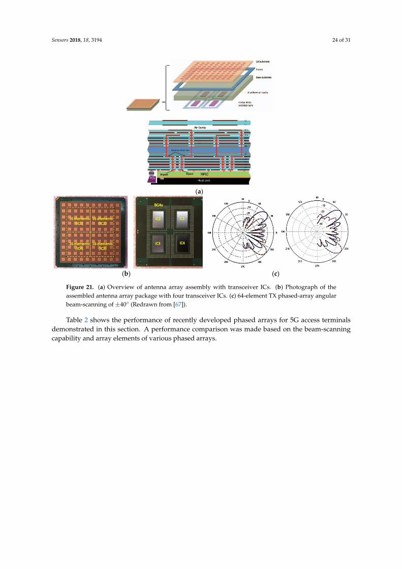
Sensors 2018, 18, 3194 24 of 31
Sensors 2018, 18, x FOR PEER REVIEW 25 of 33
(b)
(c)
Figure 20. (a) Block diagram of 2 × 2 transmit/receive 5G phased array. (b) Photograph of the flip-chip
test board with 2 × 2 transmit/receive 5G phased array. (c) Measured E and H-plane patterns of 4 × 8
transmit/receive 5G phased array in Rx mode (Redrawn from [54,60]).
In [67], a multilayer 64-element dual-polarized antenna-in-package assembly with four-SiGe
BiCMOS multi-chip phased array operating at 28 GHz was proposed for 5G mm-wave
communication. The proposed module has four mounted SiGe BiCMOS transceiver ICs supporting
dual polarization in Tx and Rx modes. The proposed antenna array has a 3-GHz bandwidth at an
operating frequency of 28 GHz. The measured Tx gain is around 35 dBi for the 64-element antenna
array. The angular beam-scanning of ±40° in the azimuth and elevation plane was achieved, as shown
in Figure 21c.
(a)
(b)
(c)
Figure 21. (a) Overview of antenna array assembly with transceiver ICs. (b) Photograph of theassembled antenna array package with four transceiver ICs. (c) 64-element TX phased-array angularbeam-scanning of ±40 (Redrawn from [67]).
Table 2 shows the performance of recently developed phased arrays for 5G access terminalsdemonstrated in this section. A performance comparison was made based on the beam-scanningcapability and array elements of various phased arrays.

Sensors 2018, 18, 3194 25 of 31
Table 2. Performance variation of various phased arrays for 5G access terminals.
Ref # Array/ICElements
Elements inPackage
TX/RX PolarizationsPer IC fo (GHz) Beam-Scanning
(deg)Gain (Tx/Rx)
(dBi) Technology TX/RXInterface
Package Specification / IntegrationLevel
[9] 32 × 32 1024 - 28 - - Single-layer PCB - (HUST) Array Antenna architecture
[13] 6 × 8 48 - 28 ±110 21 Single-layer PCB - (Samsung) MIMOAntenna transceiver
[39] 1 × 7 7 - 28 ±27 24.2 Multilayer PCB - Antenna only
[15] 16 × 4 64 - 28 ±67 29/27 Single-layer PCB - (Bell Labs) MIMO transceiver withDBF architecture
[55] 4 × 8 32 - 27.925 ±30 18 Single-layer PCB - (Samsung) ArrayAntenna architecture
[53,65] 16 × 2 128 2/2 28 ±50 32/34 0.13 µmSiGe BiCMOS 3 GHz IF (IBM) Antenna in package
[54,60] 2 × 2 4 1/1 29 ±50, ±25 18/12 0.18 µmSiGe BiCMOS RF (UCSD) Antenna on PCB
[61] 2 × 4 8 1/1 28 ±20 14 28 nm CMOS Analog IQ BB (LG) Antenna in package
[63] 4 × 6 24 2/2 28 ±45 44/34 28 nm CMOS 6.5 GHz IF (Qualcomm) Antenna in package
[66] 2 × 2 4 - 28 ±45 - Multilayer PCB andFlip-chip module - (Qualcomm) Antenna on PCB with
packaged ICs
[67] 4 × 4 64 2/2 28 ±40 35 Multilayer PCB +4 SiGe BiCMOS
3 GHz IFinterface (IBM) Antenna in package

Sensors 2018, 18, 3194 26 of 31
3. Discussion
Although mm-wave technology is being considered overall for future 5G wireless communicationsystems, there remains the need for improvement and changes in current mm-wave architectures andthe expected commercial designs to be used in mm-wave cellular communication networks [4,6,9].A few basic improvements are required with respect to the deployment and implementation ofmm-wave cellular networks. Sophisticated antenna array designs are proposed to improve theperformance of wireless communication systems in terms of high gain and coverage area. Becausethere is a trade-off between the gain and bandwidth, phased arrays structures offer an increasedangular beam-scanning range along with high gain [70]. Various types of phased-array structures havebeen developed in the last few years. For the BS array antenna, there remains a relaxation of the spacefactor for designing complicated phased-array designs with increased spatial beam-scanning. However,in the case of MS antennas, it is more demanding to implement phased arrays in cellular handsetsbecause of the limited space, user mobility, and user effects. Therefore, in this article, we discussed indetail the design constraints and implementation challenges of mm-wave phased arrays for 5G mobileterminals (MSs) and access terminals (BSs).
To obtain the directional fan-beam radiation patterns in both the vertical and horizontal directions,two separate phased arrays positioned on the top and bottom of the chassis of a cellular handset weredemonstrated in [10]. In [49], 3D beam-scanning was achieved by employing a folded 3D structureusing three subarrays at the top position, but there is a limitation in terms of the implementation of the3D array structure in the cellular handset. To address this limitation, 3D coverage was achieved in [50]using the surface waves of three identical slotted subarrays by switching the main beam direction toseparate regions. Each subarray behaves similar to a phased array to tilt the beam to a separate region.
To address the polarization mismatch [7,46] and incurred losses owing to the mobility of the userand various kinds of motions experienced by the mobile terminals at different angles, multi-polarized,i.e., horizontally polarized and vertically polarized antennas are combined in a subarray to achievethe diversity gain, while enhancing the efficiency of the transmission and reception at mm-wavefrequencies [47]. To achieve polarization diversity along with the enhanced bandwidth, printedhorizontally polarized and vertically polarized quasi-Yagi-Uda antennas were implemented [51].Enhanced beam-scanning is achieved by combining horizontally polarized and vertically polarizedantennas in an array using the side-by-side placement of these subarrays in a cellular handset [44,47].
Because of the constraints of space and position in cellular handsets, much research has beenperformed on the structure of mm-wave phased arrays with different handset positions [28,37,41,50].Most of the phased arrays for 5G mobile terminals are single-layer substrate planar phased arrays tobetter fit into the chassis of cellular phones [42,48–50]. Further research efforts have been attempted onmultilayer mesh-grid phased arrays [7] and SIW phased arrays [37].
Although most research has been performed on low-cost substrate boards [71,72], such asPCB-based phased arrays, there is little compliance with the metallic frame casing of modern cellulardevices [56,57]. However, the study in [41] introduced a set of two eight-element cavity-backed slottedsubarrays on both sides of the metallic casing of a cellular device. The study in [40] illustrates thedegree to which the human body is vulnerable to electromagnetic fields (EMF) owing to the designedphased-array antennas in terms of the specific absorption rate (SAR). The authors in [40] successfullyreduced the SAR to 0.88 W/kg by using slotted subarrays on the top and back of the metallic casing ofa cellular handset.
To address the increased path loss at mm-wave frequencies and the lower power consumptioncompared to that of sub-6-GHz communication links, LOS communication using phased-arraytechniques with an array antenna gain is required. Various antenna array architecture designsfor outdoor mm-wave communication with different beamforming techniques, i.e., analog, digital,and hybrid techniques, were analyzed [9]. The antenna array design with circular elements ismore robust to vibrations and is therefore the best candidate for outdoor mm-wave communicationin terms of beam gain, gain fluctuation, and beam misalignment of phased-array antennas.

Sensors 2018, 18, 3194 27 of 31
Analog beamforming compensates for the high path loss by generating high beamforming gains,whereas digital beamforming presents a better performance with an enhanced structural complexity.Therefore, a combination of analog and digital beamforming array architectures on both the transmitterand receiver ends has become the focus of research in recent years days based on the trade-off betweenthe flexibility and performance in outdoor mm-wave communications [55,73].
Cost is an important factor that needs to be significantly lowered owing to the widespread useof phased arrays in 5G wireless communication. Therefore, ICs that are based on silicon technology(SiGe or BiCMOS) [34,35,54,58,59] along with low-cost PCB technology [35,36,60] should be considered.Scalable, RFIC-based phased arrays that are capable of beam-scanning in both the horizontal andvertical planes currently attract much attention from researchers [60].
4. Conclusions
In this review, article, we demonstrated recently proposed phased arrays for 5G mobile terminalsand access terminals. These state-of-the-art phased arrays are compact in size, low-cost, and haveenough beam-scanning and coverage range. The effects of the user’s body and human exposure toEM waves by these state-of-the-art phased arrays with 3D coverage designed on single-layer andmultilayer substrates were illustrated. In addition, multi-polarized antenna arrays and the spaceconstraints of mobile terminals were presented and discussed. Various beamforming techniques usingstate-of-the-art mm-wave phased-array architectures to mitigate the co-channel interference and toovercome the path loss were proposed.
Author Contributions: S.L. conceived the idea for the study and A.H.N. wrote the manuscript. S.L. revised themanuscript and ensured conciseness.
Acknowledgments: This research was supported by the National Research Foundation of Korea (NRF) grantfunded by the Korean government (MSIT) (2018R1A4A1023826).
Conflicts of Interest: The authors declare no conflict of interest.
References
1. Parker, D.; Zimmermann, D.C. Phased arrays—Part 1: Theory and architectures. IEEE Trans. Microw.Theory Tech. 2002, 50, 678–687. [CrossRef]
2. Niknejad, A.M.; Hashemi, H. Integrated Beamforming Arrays. In mm-Wave Silicon Technology; Series onIntegrated Circuits and Systems; Springer Science and Business Media: Berlin, Germany, 2008;ISBN 978-0-387-76561-7.
3. Carpentieri, E.; Elia, U.F.D.; Stefano, E.D.; Guida, L.D.; Vitiello, R. Millimeter-Wave Phased-Array Antennas.In Proceedings of the IEEE Radar Conference, Rome, Italy, 26–30 May 2008; pp. 1–5.
4. Dahlman, E.; Mildh, G.; Parkvall, S.; Peisa, J.; Sachs, J.; Selen, Y.; Skold, J. 5G wireless access: Requirementsand realization. IEEE Commun. Mag. 2014, 52, 42–47. [CrossRef]
5. Marcus, M.J. 5G and “IMT for 2020 and beyond” [Spectrum Policy and Regulatory Issues]. IEEE Wirel. Commun.2015, 22, 2–3. [CrossRef]
6. Rappaport, T.S.; Sun, S.; Mayzus, R.; Zhao, H.; Azar, Y.; Wang, K.; Wong, G.N.; Schulz, J.K.; Samimi, M.;Gutierrez, F. Millimeter wave mobile communications for 5G cellular: It will work! IEEE Access 2013, 1,335–349. [CrossRef]
7. Hong, W.; Baek, K.H.; Ko, S. Millimeter-Wave 5G Antennas for Smartphones: Overview and ExperimentalDemonstration. IEEE Trans. Antennas Propag. 2017, 65, 6250–6261. [CrossRef]
8. Pi, Z.; Khan, F. An introduction to millimeter-wave mobile broadband systems. IEEE Commun. Mag. 2011,49, 101–107. [CrossRef]
9. Zhang, J.; Ge, X.; Li, Q.; Guizani, M.; Zhang, Y. 5G Millimeter-Wave Antenna Array: Design and Challenges.IEEE Wirel. Commun. 2017, 24, 106–112. [CrossRef]
10. Hong, W.; Baek, K.H.; Lee, Y.; Kim, Y.; Ko, S.T. Study and prototyping of practically large-scale mmWaveantenna systems for 5G cellular devices. IEEE Commun. Mag. 2014, 52, 63–69. [CrossRef]

Sensors 2018, 18, 3194 28 of 31
11. Dehos, C.; González, J.; Domenico, A.; Kténas, D.; Dussopt, L. Millimeter-wave access and backhauling:The solution to the exponential data traffic increase in 5G mobile communications systems? IEEE Commun. Mag.2014, 52, 88–95. [CrossRef]
12. Dussopt, L.; Bouayadi, O.E.; Alberto, J.; Luna, Z.; Dehos, C.; Lamy, Y. Millimeter-Wave Antennas for RadioAccess and Backhaul in 5G Heterogeneous Mobile Networks. In Proceedings of the 9th European Conferenceon Antennas and Propagation, Lisbon, Portugal, 12–17 April 2015; pp. 1–4.
13. Kim, Y.; Lee, H.Y.; Hwang, P.; Patro, R.K.; Lee, J.; Roh, W.; Cheun, K. Feasibility of Mobile CellularCommunications at Millimeter Wave Frequency. IEEE J. Sel. Top. Signal. Process. 2016, 10, 589–599.[CrossRef]
14. Hur, S.; Kim, T.; Love, D.J.; Krogmeier, J.V.; Thomas, T.A.; Ghosh, A. Millimeter wave beamforming forwireless backhaul and access in small cell networks. IEEE Trans. Commun. 2013, 61, 4391–4403. [CrossRef]
15. Yang, B.; Yu, Z.; Lan, J.; Zhang, R.; Zhou, J.; Hong, W. Digital Beamforming-Based Massive MIMO Transceiverfor 5G Millimeter-Wave Communications. IEEE Trans. Microw. Theory Tech. 2018, 1–16. [CrossRef]
16. Helander, J.; Sjoberg, D.; Gustafsson, M.; Zhao, K.; Ying, Z. Characterization of millimeter wave phased arrayantennas in mobile terminal for 5G mobile system. In Proceedings of the IEEE International Symposiumon Antennas and Propagation & USNC/URSI National Radio Science Meeting, Vancouver, BC, Canada,7–8 October 2015; pp. 7–8.
17. Rajagopal, S.; Surra, S.A.; Pi, Z.; Khan, F. Antenna array design for multi-Gbps millimeter wave mobilebroadband communication. In Proceedings of the Global Telecommunications Conference (GLOBECOM2011), Houston, TX, USA, 5–9 December 2011; pp. 1–6.
18. Wang, J.J.H.; Corporation, W.E. Wideband Wide-Scan Millimeter-Wave Phased Arrays for EnhancedSecurity/Privacy and Performance in 5G Mobile Wireless. In Proceedings of the IEEE InternationalSymposium on Antennas and Propagation & USNC/URSI National Radio Science Meeting, San Diego, CA,USA, 9–14 July 2017; pp. 1471–1472.
19. Bas, C.U.; Wang, R.; Psychoudakis, D.; Henige, T.; Monroe, R.; Park, J.; Zhang, J.; Molisch, A.F. A real-timemillimeter-wave phased array MIMO channel sounder. In Proceedings of the IEEE 86th Vehicular TechnologyConference: VTC2017-Fall, Toronto, ON, Canada, 24–27 September 2017; pp. 1–6.
20. Niu, Y.; Li, Y.; Jin, D.; Su, L.; Vasilakos, A.V. A survey of millimeter wave communications (mmWave) for 5G:Opportunities and challenges. Wirel. Netw. 2015, 21, 2657–2676. [CrossRef]
21. Brady, J.; Hogan, J.; Sayeed, A. Multi-beam MIMO prototype for real-time multiuser communication at28 GHz. In Proceedings of the Globecom Workshops (GC Wkshps), Washington, DC, USA, 4–8 December2016; pp. 1–6.
22. Han, S.; Chih-Lin, I.; Xu, Z.; Rowell, C. Large-scale antenna systems with hybrid analog and digitalbeamforming for millimeter wave 5G. IEEE Commun. Mag. 2015, 53, 186–194. [CrossRef]
23. Alexandropoulos, G.C. Position Aided Beam Alignment for Millimeter Wave Backhaul Systems with LargePhased Arrays. In Proceedings of the IEEE 7th International Workshop on Computational Advances inMulti-Sensor Adaptive Processing (CAMSAP), Curacao, The Netherlands, 10–13 December 2017; pp. 1–5.
24. Hong, W.; Jiang, Z.H.; Yu, C.; Zhou, J.; Chen, P.; Yu, Z.; Zhang, H.; Yang, B.; Pang, X.; Jiang, M.; et al.Multibeam Antenna Technologies for 5G Wireless Communications. IEEE Trans. Antennas Propag. 2017, 65,6231–6249. [CrossRef]
25. Björnson, E.; Van der Perre, L.; Buzzi, S.; Larsson, E.G. Massive MIMO in Sub-6 GHz and mmWave: Physical,Practical, and Use-Case Differences. arXiv, 2018; arXiv:1803.11023.
26. Cai, M.; Laneman, J.N.; Hochwald, B. Carrier Aggregation for Phased-Array Analog Beamforming withBeam Squint. In Proceedings of the 2017 IEEE GLOBECOM, Singapore, 4–8 December 2017.
27. Abbaspour-Tamijani, A.; Sarabandi, K. An Affordable Millimeter-Wave Beam-Steerable Antenna UsingInterleaved Planar Subarrays. IEEE Trans. Antennas Propag. 2003, 51, 2193–2202. [CrossRef]
28. Helander, J.; Zhao, K.; Ying, Z.; Sjoberg, D. Performance Analysis of Millimeter Wave Phased Array Antennasin Cellular Handsets. IEEE Antennas Wirel. Propag. Lett. 2015, 1225. [CrossRef]
29. Rappaport, T.S.; Gutierrez, F.; Ben-Dor, E.; Murdock, J.N.; Qiao, Y.; Tamir, J.I. Broadband millimeter-wavepropagation measurements and models using adaptive-beam antennas for outdoor Urban cellularcommunications. IEEE Trans. Antennas Propag. 2013, 61, 1850–1859. [CrossRef]
30. Adabi, E.; Floyd, B. mm-Wave Silicon Technology: 60 GHz and Beyond; Springer Science and Business Media:New York, NY, USA, 2008; ISBN 978-0-387-76558-7.

Sensors 2018, 18, 3194 29 of 31
31. Lai, C.H.; Ma, T.G. Applications to Heterogeneous Integrated Phased Arrays. In Synthesized TransmissionLines: Design, Circuit Implementation, and Phased Array Applications; John Wiley & Sons: Singapore, 2016;pp. 96–125.
32. Emami, S.; Wiser, R.F.; Ali, E.; Forbes, M.G.; Gordon, M.Q.; Guan, X.; Lo, S.; McElwee, P.T.; Parker, J.;Tani, J.R.; et al. A 60GHz CMOS phased-array transceiver pair for multi-Gb/s wireless communications.In Proceedings of the 2011 IEEE International Solid-State Circuits Conference, San Francisco, CA, USA,20–24 February 2011; Volume 40, pp. 164–165. [CrossRef]
33. Slezak, C.; Dhananjay, A.; Rangan, S. 60 GHz Blockage Study Using Phased Arrays. In Proceedings ofthe 2017 Asilomar Conference on Signals, Systems, and Computers, Pacific Grove, CA, USA, 29 October–1 November 2017; pp. 1655–1659.
34. Natarajan, A.; Reynolds, S.K.; Tsai, M.D.; Nicolson, S.T.; Zhan, J.H.C.; Kam, D.G.; Liu, D.; Huang, Y.L.O.;Valdes-Garcia, A.; Floyd, B.A. A fully-integrated 16-element phased-array receiver in SiGe BiCMOS for60-GHz communications. IEEE J. Solid-State Circuits 2011, 46, 1059–1075. [CrossRef]
35. Rebeiz, G.M.; Kim, S.Y.; Inac, O.; Shin, W.; Gurbuz, O.; Ou, Y.C.; Golcuk, F.; Kanar, T.; Ku, B.H.Millimeter-wave large-scale phased-arrays for 5G systems. In Proceedings of the Microwave, MTT-SInternational Symposium, San Francisco, CA, USA, 17–22 May 2015; pp. 28–30.
36. Chen, Z.; Zhang, Y.P. FR4 PCB grid array antenna for millimeter-wave 5G mobile communications.In Proceedings of the Microwave Workshop Series on RF and Wireless Technologies for Biomedical andHealthcare Applications (IMWS-BIO), Singapore, 9–11 December 2013; pp. 13–15.
37. Yang, Q.L.; Ban, Y.L.; Kang, K.; Sim, C.Y.D.; Wu, G. SIW Multibeam Array for 5G Mobile Devices. IEEE Access2016, 4, 2788–2796. [CrossRef]
38. Ala-Laurinaho, J.; Aurinsalo, J.; Karttunen, A.; Kaunisto, M.; Lamminen, A.; Nurmiharju, J.; Raisanen, A.V.;Saily, J.; Wainio, P. 2-D Beam-Steerable Integrated Lens Antenna System for 5G E-Band Access and Backhaul.IEEE Trans. Microw. Theory Tech. 2016, 64, 2244–2255. [CrossRef]
39. Jiang, M.; Chen, Z.N.; Zhang, Y.; Hong, W.; Xuan, X. Metamaterial-Based Thin Planar Lens Antenna forSpatial Beamforming and Multibeam Massive MIMO. IEEE Trans. Antennas Propag. 2017, 65, 464–472.[CrossRef]
40. Bang, J.; Choi, J. A SAR Reduced MM-Wave Beam-Steerable Array Antenna with Dual-Mode Operation forFully Metal—Covered 5G Cellular Handsets. IEEE Antennas Wirel. Propag. Lett. 2018, 1225. [CrossRef]
41. Yu, B.; Yang, K.; Sim, C.; Yang, G. A Novel 28 GHz Beam Steering Array for 5G Mobile Device With MetallicCasing Application. IEEE Trans. Antennas Propag. 2018, 66, 462–466. [CrossRef]
42. Syrytsin, I.; Zhang, S.; Pedersen, G.F.; Ieee, S.M.; Morris, A. Compact Quad-Mode Planar Phased Array withWideband for 5G Mobile Terminals. IEEE Trans. Antennas Propag. 2018. [CrossRef]
43. Liu, S.T.; Hsu, Y.W.; Lin, Y.C. A dual polarized cavity-backed aperture antenna for 5G mmW MIMOapplications. In Proceedings of the Microwaves, Communications, Antennas and Electronic Systems(COMCAS), Tel Aviv, Israel, 2–4 November 2015; p. 4.
44. Hong, W. Compact 28 GHz Antenna Array with Full Polarization Flexibility Under Yaw, Pitch, Roll Motions.In Proceedings of the 9th European Conference on Antennas and Propagation (EuCAP), Lisbon, Portugal,13–17 April 2015; pp. 1–3.
45. Chuang, N.C.; Lin, H.S.; Lin, Y.C. Compact cavity-backed dual-polarized aperture antennas for millimeterwave MIMO applications. In Proceedings of the Microwaves for Intelligent Mobility (ICMIM), Nagoya, Japan,19–21 March 2017; pp. 131–134.
46. Hong, W.; Ko, S.T.; Lee, Y.; Baek, K.H. Multi-polarized antenna array configuration for mmWave 5G mobileterminals. In Proceedings of the 2015 International Workshop on Antenna Technology (iWAT), Seoul, Korea,4–6 March 2015; pp. 60–61.
47. Hsu, Y.W.; Huang, T.C.; Lin, H.S.; Lin, Y.C. Dual-Polarized Quasi Yagi-Uda Antennas with Endfire Radiationfor Millimeter-Wave MIMO Terminals. IEEE Trans. Antennas Propag. 2017, 65, 6282–6289. [CrossRef]
48. Ojaroudiparchin, N.; Shen, M.; Pedersen, G.F. Design of Vivaldi antenna array with end-fire beam steeringfunction for 5G mobile terminals. In Proceedings of the 2015 23rd Telecommunications Forum Telfor(TELFOR), Belgrade, Serbia, 24–26 November 2015; pp. 587–590. [CrossRef]
49. Ojaroudiparchin, N.; Shen, M.; Zhang, S.; Pedersen, G.F. A Switchable 3-D-Coverage-Phased Array AntennaPackage for 5G Mobile Terminals. IEEE Antennas Wirel. Propag. Lett. 2016, 15, 1747–1750. [CrossRef]

Sensors 2018, 18, 3194 30 of 31
50. Zhang, S.; Chen, X.; Syrytsin, I.; Pedersen, G.F. A Planar Switchable 3-D-Coverage Phased Array Antennaand Its User Effects for 28-GHz Mobile Terminal Applications. IEEE Trans. Antennas Propag. 2017, 65,6413–6421. [CrossRef]
51. Alhalabi, R.A.; Rebeiz, G.M. High-gain yagi-uda antennas for millimeter-wave switched-beam systems.IEEE Trans. Antennas Propag. 2009, 57, 3672–3676. [CrossRef]
52. Garg, R.; Natarajan, A.S. A 28-GHz Low-Power Phased-Array Receiver Front-End with 360 RTPS PhaseShift Range. IEEE Trans. Microw. Theory Tech. 2017, 65, 4703–4714. [CrossRef]
53. Sadhu, B.; Tousi, Y.; Hallin, J.; Sahl, S.; Reynolds, S.; Renstrom, O.; Sjogren, K.; Haapalahti, O.; Mazor, N.;Bokinge, B.; et al. A 28GHz 32-element phased-array transceiver IC with concurrent dual polarized beamsand 1.4-degree beam-steering resolution for 5G communication. In Proceedings of the 2017 IEEE InternationalSolid-State Circuits Conference (ISSCC), San Francisco, CA, USA, 5–9 February 2017; pp. 128–129.
54. Kibaroglu, K.; Sayginer, M.; Rebeiz, G.M. A quad-core 28-32 GHz transmit/receive 5G phased-array ICwith flip-chip packaging in SiGe BiCMOS. In Proceedings of the 2017 IEEE MTT-S International MicrowaveSymposium (IMS), Honololu, HI, USA, 4–9 June 2017; pp. 1892–1894. [CrossRef]
55. Roh, W.; Seol, J.Y.; Park, J.; Lee, B.; Lee, J.; Kim, Y.; Cho, J.; Cheun, K.; Aryanfar, F. Millimeter-WaveBeamforming as an Enabling Technology for 5G Cellular Communications: Theoretical Feasibility andPrototype Results. IEEE Commun. Mag. 2014, 52, 106–113. [CrossRef]
56. Chang, C.K.; Liao, W.J.; Tsai, C.C. Metal Body-Integrated Open-End Slot-Antenna Designs for Handset LTEUses. IEEE Trans. Antennas Propag. 2016, 64, 5436–5440. [CrossRef]
57. Bang, J.; Hong, Y.; Choi, J. MM-Wave Phased Array Antenna for Whole-Metal-Covered 5G Mobile PhoneApplications. In Proceedings of the International Symposium on Antennas and Propagation (ISAP),Phuket, Thailand, 30 October–2 November 2017; pp. 5–6.
58. Koh, K.J.; May, J.W.; Rebeiz, G.M. A millimeter-wave (4045 GHz) 16-element phased-array transmitter in0.18-µm SiGe BiCMOS technology. IEEE J. Solid-State Circuits 2009, 44, 1498–1509. [CrossRef]
59. Hashemi, H.; Guan, X.; Komijani, A.; Hajimiri, A. A 24-GHz SiGe phased-array receiver-LO phase-shiftingapproach. IEEE Trans. Microw. Theory Tech. 2005, 53, 614–625. [CrossRef]
60. Kibaroglu, K.; Sayginer, M.; Rebeiz, G.M. A Low-Cost Scalable 32-Element 28-GHz Phased Array Transceiverfor 5G Communication Links Based on a Beamformer Flip-Chip Unit Cell. IEEE J. Solid-State Circuits 2018,53, 1260–1274. [CrossRef]
61. Kim, H. A 28-GHz CMOS Direct Conversion Transceiver with Packaged 2 × 4 Antenna Array for 5G CellularSystem. IEEE J. Solid-State Circuits 2018, 53, 1245–1259. [CrossRef]
62. Kim, H. A 28GHz CMOS direct conversion transceiver with packaged antenna arrays for 5G cellular system.In Proceedings of the 2017 IEEE Radio Frequency Integrated Circuits Symposium (RFIC 2017), Honolulu, HI,USA, 4–6 June 2017; pp. 69–72.
63. Dunworth, J.D. A 28GHz Bulk-CMOS dual-polarization phased-array transceiver with 24 channels for5G user and base station equipment. In Proceedings of the IEEE International Solid-State CircuitsConference-(ISSCC), San Francisco, CA, USA, 11–15 February 2018; pp. 70–72.
64. Du, J. Dual-polarized patch array antenna package for 5G communication systems. In Proceedings ofthe 11th European Conference on Antennas and Propagation (EUCAP), Paris, France, 19–24 March 2017;pp. 3493–3496.
65. Sadhu, B. A 28-GHz 32-Element TRX Phased-Array IC With Concurrent Dual-Polarized Operation andOrthogonal Phase and Gain Control for 5G Communications. IEEE J. Solid-State Circuits 2017, 52, 3373–3391.[CrossRef]
66. Jeong, N.S.; Ou, Y.; Tassoudji, A.; Dunworth, J.; Koymen, O.; Raghavan, V. A recent development ofantenna-in-package for 5G millimeter-wave applications. In Proceedings of the 19th annual IEEE Wirelessand Microwave Technology Conference (WAMICON 2018), Sand Key, FL, USA, 4–9 April 2018; pp. 1–3.
67. Gu, X. A multilayer organic package with 64 dual-polarized antennas for 28GHz 5G communication.In Proceedings of the IEEE International Microwave Symposium (IMS2017), Honololu, HI, USA, 4–9 June 2017;pp. 1899–1901.
68. Gu, X.; Sadhu, B.; Liu, D.; Baks, C.; Valdes-Garcia, A. Antenna-in-package design and module integration formillimeter-wave communication and 5G. In Proceedings of the The 2018 International Symposium on VLSIDesign, Automation and Test, Hsinchu, Taiwan, 16–19, April 2018; pp. 1–2.

Sensors 2018, 18, 3194 31 of 31
69. Valdes-Garcia, A. Circuit and antenna-in-package innovations for scaled mmWave 5G phased array modules.In Proceedings of the 2018 IEEE Custom Integrated Circuits Conference (CICC), San Diego, CA, USA,8–11 April 2018; pp. 1–8.
70. Bondyopadhyay, P.K. The first application of array antenna. In Proceedings of the IEEE InternationalConference on Phased Array Systems and Technology, Dana Point, CA, USA, 21–25 May 2000; pp. 29–32.
71. Niamat, H.; Kedze, K.; Park, I. Performance of a Planar Leaky-Wave Slit Antenna for Different Values ofSubstrate Thickness. J. Electromagn. Eng. Sci. 2017, 17, 202–207. [CrossRef]
72. Mok, K.Y.; Rhee, Y.C.; Yoon, J.H. Design of a Pot-Shaped Monopole Antenna with Dual Band NotchedCharacteristics for UWB Application. J. Electromagn. Eng. Sci. 2017, 17, 44–49. [CrossRef]
73. Kwon, D.S.; Lee, S.J.; Kim, J.W.; Ahn, B.K.; Yu, J.W.; Lee, W.S. An Eight-Element Compact Low-ProfilePlanar MIMO Antenna Using LC Resonance with High Isolation. J. Electromagn. Eng. Sci. 2016, 16, 94–97.[CrossRef]
© 2018 by the authors. Licensee MDPI, Basel, Switzerland. This article is an open accessarticle distributed under the terms and conditions of the Creative Commons Attribution(CC BY) license (http://creativecommons.org/licenses/by/4.0/).