Design and Fabrication of a MEMS-Array Pressure Sensor ...
241
Design and Fabrication of a MEMS-Array Pressure Sensor System for Passive Underwater Navigation Inspired by the Lateral Line by Stephen Ming-Chang Hou M.Eng., Electrical Engineering and Computer Science Massachusetts Institute of Technology, 2004 S.B., Electrical Science and Engineering Massachusetts Institute of Technology, 2003 S.B., Physics Massachusetts Institute of Technology, 2003 Submitted to the Department of Electrical Engineering and Computer Science in partial fulfillment of the requirements for the degree of Electrical Engineer at the MASSACHUSETTS INSTITUTE OF TECHNOLOGY June 2012 c Massachusetts Institute of Technology 2012. All rights reserved. Author ............................................................................ Department of Electrical Engineering and Computer Science March 14, 2012 Certified by ........................................................................ Jeffrey H. Lang Professor of Electrical Engineering Thesis Supervisor Accepted by ....................................................................... Leslie A. Kolodziejski Chair, Department Committee on Graduate Theses
-
Upload
khangminh22 -
Category
Documents
-
view
3 -
download
0
Transcript of Design and Fabrication of a MEMS-Array Pressure Sensor ...
Design and Fabrication of a MEMS-Array Pressure Sensor
System for Passive Underwater Navigation Inspired by the
Lateral Line
by
Stephen Ming-Chang Hou
M.Eng., Electrical Engineering and Computer Science
Massachusetts Institute of Technology, 2004
S.B., Electrical Science and Engineering
Massachusetts Institute of Technology, 2003
S.B., Physics
Massachusetts Institute of Technology, 2003
Submitted to the Department of Electrical Engineering and Computer Science
in partial fulfillment of the requirements for the degree of
Electrical Engineer
at the
MASSACHUSETTS INSTITUTE OF TECHNOLOGY
June 2012
c© Massachusetts Institute of Technology 2012. All rights reserved.
Author . . . . . . . . . . . . . . . . . . . . . . . . . . . . . . . . . . . . . . . . . . . . . . . . . . . . . . . . . . . . . . . . . . . . . . . . . . . .
Department of Electrical Engineering and Computer Science
March 14, 2012
Certified by. . . . . . . . . . . . . . . . . . . . . . . . . . . . . . . . . . . . . . . . . . . . . . . . . . . . . . . . . . . . . . . . . . . . . . . .
Jeffrey H. Lang
Professor of Electrical Engineering
Thesis Supervisor
Accepted by . . . . . . . . . . . . . . . . . . . . . . . . . . . . . . . . . . . . . . . . . . . . . . . . . . . . . . . . . . . . . . . . . . . . . . .
Leslie A. Kolodziejski
Chair, Department Committee on Graduate Theses

2
Design and Fabrication of a MEMS-Array Pressure Sensor System for
Passive Underwater Navigation Inspired by the Lateral Line
by
Stephen Ming-Chang Hou
Submitted to the Department of Electrical Engineering and Computer Scienceon March 14, 2012, in partial fulfillment of the
requirements for the degree ofElectrical Engineer
Abstract
An object within a fluid flow generates local pressure variations that are unique and char-acteristic to the object’s shape and size. For example, a three-dimensional object or awall-like obstacle obstructs flow and creates sharp pressure gradients nearby. Similarly, un-steady flow contains vortical patterns with associated unique pressure signatures. Detectionof obstacles, as well as identification of unsteady flow features, is required for autonomousundersea vehicle (AUV) navigation. An array of passive underwater pressure sensors, withtheir ability to “touch at a distance” with minimal power consumption, would be able toresolve the pressure signatures of obstacles in the near field and the wake of objects in theintermediate field. As an additional benefit, with proper design, pressure sensors can alsobe used to sample acoustic signals as well.
Fish already have a biological version of such a pressure sensor system, namely the lateralline organ, a spatially-distributed set of sensors over a fish’s body that allows the fish tomonitor its hydrodynamic environment, influenced by the external disturbances. Throughits ability to resolve the pressure signature of objects, the fish obtains “hydrodynamicpictures”.
Inspired by the fish lateral line, this thesis describes the development of a high-densityarray of microelectromechanical systems (MEMS) pressure sensors built in KOH-etchedsilicon and HF-etched Pyrex wafers. A novel strain-gauge resistor design is discussed,and standard CMOS/MEMS fabrication techniques were used to build sensors based onthe strain-gauge resistors and thin silicon diphragms. Measurements of the diaphragmdeflection and strain-gauge resistance changes in response to changes in applied externalpressure confirm that the devices can be reliably calibrated for use as pressure sensors toenable passive navigation by AUVs. A set of sensors with millimeter-scale spacing, 2.1 to2.5 µV/Pa sensitivity, sub-pascal pressure resolution, and −2000 Pa to 2000 Pa pressurerange has been demonstrated. Finally, an integrated circuit for array processing and signalamplification and to be fabricated with the pressure sensors is proposed.
Thesis Supervisor: Jeffrey H. LangTitle: Professor of Electrical Engineering
3

4
Acknowledgments
This thesis would not have been possible without the efforts of many people. First, I would
like to express gratitude to my advisor, Prof. Jeff Lang, for the opportunity to work under
his mentorship throughout my graduate studies. His deep intuition and focus on important
questions will always influence me. I thank the other faculty under whom I have worked
on various projects over the years, Profs. Franz Hover, Marty Schmidt, Alex Slocum and
Michael Triantafyllou, for their creative insights and guidance. Their boundless supply of
energy, enthusiasm and knowledge make MIT such an incredible place to study.
I would like to thank the other members of the Underwater Sensors Group and the
Precision Engineering Research Group. I am grateful to my officemate Dr. Vicente Fer-
nandez, who worked on complementary aspects of our overall project, for our conversations
and mutual encouragement. I am especially thankful to Drs. Hong Ma, Alexis Weber and
James White for their many hours showing me the ropes in the lab when I first started, and
generously providing many pieces of advice throughout, even when they were busy prepar-
ing to graduate. Drs. Jian Li, Joachim Sihler and Xue’en Yang also extended invaluable
tips on fabrication techniques.
I would like to thank other members of the MEMS community at MIT. In particular,
I thank Prof. Joel Voldman for sharing his experience with HF etching. I would like to
thank Kevin Nagy and Dr. Nikolay Zaborenko for their bonding recipes, and countless
other fabrication laboratory users for sharing bits of advice, which has motivated me to
contribute to our collective knowledge.
In the spirit of the collaborative nature of MIT, I thank Drs. Steve Bathurst, Jerry Chen,
Ivan Nausieda and Vanessa Wood for sharing their laboratory equipment for experimenting
with printable electronics.
I would like to express great appreciation for the MIT Microsystems Technology Lab-
oratories (MTL), i.e. my second home, where my fabrication work was carried out. In
particular, I am grateful to MTL staff members Bernard Alamariu, Bob Bicchieri, Kurt
Broderick, Eric Lim, Kris Payer, Dave Terry, Paul Tierney, Tim Turner and Dennis Ward,
who patiently trained me on each of the machines, maintained tools around the clock,
answered my calls and e-mails when I needed help, and offered advice.
5

I thank Pierce Hayward for training me to use the Zygo profilometer. I am also grateful
to Wayne Ryan and Steve Turschmann for building various equipment that my research
required.
I would like to thank the National Science Foundation, the NOAA MIT Sea Grant
College Program (project grant R/RT-2/RCM-17), the MIT-Singapore Alliance, the MIT
Deshpande Center and the MIT Department of Electrical Engineering and Computer Sci-
ence (EECS) for their funding of my research.
I would like to thank Sam Chang, Dr. Shahriar Khushrushahi, Adam Reynolds, Yasu
Shirasaki and my family for taking the time to read my thesis and offer improvements,
especially on short notice. However, any outstanding errors are mine alone.
Of course, I am grateful to those at MIT who have provided me with a life outside the
lab. I will always remember my friends from the Graduate Student Council, the EECS
Graduate Students Association, the Resources for Easing Friction and Stress and Ashdown
House for inspiring a selfless sense of community and belonging. I also appreciate the EECS
department, the Educational Studies Program and BLOSSOMS for the distinct privilege of
teaching bright young people on behalf of MIT.
Finally, I would like to thank my family for their unwavering support and encourage-
ment. I am indebted to my parents’ dedicated efforts in providing me the opportunities
I’ve had throughout my life. Their eternal love and faith in me will be carried to future
generations. I dedicate this thesis to them.
6

Contents
1 Introduction 21
1.1 The Fish Lateral Line and Biomimetics . . . . . . . . . . . . . . . . . . . . 24
1.2 MEMS Pressure Sensors: A Broader Context . . . . . . . . . . . . . . . . . 27
1.3 Where This Work Fits In . . . . . . . . . . . . . . . . . . . . . . . . . . . . 32
1.4 Project Summary . . . . . . . . . . . . . . . . . . . . . . . . . . . . . . . . . 35
1.5 Thesis Organization . . . . . . . . . . . . . . . . . . . . . . . . . . . . . . . 37
2 Device Design 39
2.1 Overview of Device Features . . . . . . . . . . . . . . . . . . . . . . . . . . . 40
2.2 Wafer-Level Design . . . . . . . . . . . . . . . . . . . . . . . . . . . . . . . . 43
2.2.1 Air channels . . . . . . . . . . . . . . . . . . . . . . . . . . . . . . . 43
2.2.2 Round 1 . . . . . . . . . . . . . . . . . . . . . . . . . . . . . . . . . . 44
2.2.3 Round 2 . . . . . . . . . . . . . . . . . . . . . . . . . . . . . . . . . . 45
2.2.4 Round 3 . . . . . . . . . . . . . . . . . . . . . . . . . . . . . . . . . . 48
2.2.5 Round 4 . . . . . . . . . . . . . . . . . . . . . . . . . . . . . . . . . . 50
2.2.6 Round 5 . . . . . . . . . . . . . . . . . . . . . . . . . . . . . . . . . . 50
2.3 Properties of Silicon . . . . . . . . . . . . . . . . . . . . . . . . . . . . . . . 52
2.3.1 Crystalline structure of silicon . . . . . . . . . . . . . . . . . . . . . 52
2.3.2 The elastic properties of silicon . . . . . . . . . . . . . . . . . . . . . 53
2.3.3 The elastic properties of thin silicon diaphragms . . . . . . . . . . . 55
2.4 Wheatstone Bridge Circuit . . . . . . . . . . . . . . . . . . . . . . . . . . . 57
2.5 Piezoresistive Pressure Sensors . . . . . . . . . . . . . . . . . . . . . . . . . 60
2.6 Mechanical Model of the Diaphragm . . . . . . . . . . . . . . . . . . . . . . 64
7
8 CONTENTS
2.6.1 Diaphragm assumptions . . . . . . . . . . . . . . . . . . . . . . . . . 64
2.6.2 Governing equations . . . . . . . . . . . . . . . . . . . . . . . . . . . 65
2.6.3 The nature of the deflection function . . . . . . . . . . . . . . . . . . 67
2.6.4 Deflection as a function of pressure . . . . . . . . . . . . . . . . . . . 68
2.6.5 Strain as a function of pressure . . . . . . . . . . . . . . . . . . . . . 70
2.6.6 Stress as a function of pressure . . . . . . . . . . . . . . . . . . . . . 71
2.7 Strain-Gauge Resistors . . . . . . . . . . . . . . . . . . . . . . . . . . . . . . 73
2.7.1 Relative change in resistance of an infinitesimally small resistor . . . 73
2.7.2 Simulating resistance change . . . . . . . . . . . . . . . . . . . . . . 74
2.7.3 Strain-gauge resistor pattern . . . . . . . . . . . . . . . . . . . . . . 78
2.8 Sensitivity . . . . . . . . . . . . . . . . . . . . . . . . . . . . . . . . . . . . . 80
2.9 Dynamics . . . . . . . . . . . . . . . . . . . . . . . . . . . . . . . . . . . . . 82
2.10 Summary of Expected Performance . . . . . . . . . . . . . . . . . . . . . . . 84
3 Fabrication 85
3.1 Overview of Fabrication of Round 4 Devices . . . . . . . . . . . . . . . . . . 86
3.2 Variations on Fabrication for Rounds 1, 2, 3a and 3b . . . . . . . . . . . . . 90
3.3 Photolithography . . . . . . . . . . . . . . . . . . . . . . . . . . . . . . . . . 92
3.4 Potassium Hydroxide Etching of (100) Silicon . . . . . . . . . . . . . . . . . 95
3.4.1 Silicon nitride mask and silicon oxide etch stop . . . . . . . . . . . . 96
3.4.2 Finding the crystalline plane . . . . . . . . . . . . . . . . . . . . . . 98
3.4.3 Mechanical wafer protection . . . . . . . . . . . . . . . . . . . . . . . 99
3.5 Pyrex Etching . . . . . . . . . . . . . . . . . . . . . . . . . . . . . . . . . . . 102
3.5.1 Substrate material . . . . . . . . . . . . . . . . . . . . . . . . . . . . 102
3.5.2 Process flow for etching Pyrex . . . . . . . . . . . . . . . . . . . . . 102
3.5.3 Process design for etching Pyrex . . . . . . . . . . . . . . . . . . . . 107
3.5.4 Masking materials . . . . . . . . . . . . . . . . . . . . . . . . . . . . 107
3.5.5 Pyrex etchants . . . . . . . . . . . . . . . . . . . . . . . . . . . . . . 109
3.5.6 Importance of retaining photoresist on gold . . . . . . . . . . . . . . 109
3.6 Anodic Bonding . . . . . . . . . . . . . . . . . . . . . . . . . . . . . . . . . 111

CONTENTS 9
3.7 Process Design . . . . . . . . . . . . . . . . . . . . . . . . . . . . . . . . . . 113
3.7.1 Order of key steps . . . . . . . . . . . . . . . . . . . . . . . . . . . . 113
3.7.2 Placement of insulating oxide growth step . . . . . . . . . . . . . . . 115
3.7.3 Open access to cavities . . . . . . . . . . . . . . . . . . . . . . . . . . 115
3.7.4 Wet processing bonded wafers . . . . . . . . . . . . . . . . . . . . . . 116
3.8 Mask Design . . . . . . . . . . . . . . . . . . . . . . . . . . . . . . . . . . . 117
3.8.1 List of masks . . . . . . . . . . . . . . . . . . . . . . . . . . . . . . . 117
3.8.2 Mask alignment . . . . . . . . . . . . . . . . . . . . . . . . . . . . . . 117
4 Measurements 121
4.1 Photographs of Devices . . . . . . . . . . . . . . . . . . . . . . . . . . . . . 122
4.2 Instrumentation . . . . . . . . . . . . . . . . . . . . . . . . . . . . . . . . . . 126
4.2.1 Manometer . . . . . . . . . . . . . . . . . . . . . . . . . . . . . . . . 126
4.2.2 Zygo profilometer . . . . . . . . . . . . . . . . . . . . . . . . . . . . . 128
4.2.3 Off-wafer differential amplifiers . . . . . . . . . . . . . . . . . . . . . 129
4.2.4 Tech-Etch cable . . . . . . . . . . . . . . . . . . . . . . . . . . . . . . 131
4.2.5 Water-level probe . . . . . . . . . . . . . . . . . . . . . . . . . . . . . 132
4.3 Deflection . . . . . . . . . . . . . . . . . . . . . . . . . . . . . . . . . . . . . 134
4.4 Drifting Signals . . . . . . . . . . . . . . . . . . . . . . . . . . . . . . . . . . 141
4.4.1 Experimental set up . . . . . . . . . . . . . . . . . . . . . . . . . . . 141
4.4.2 Dummy bridge . . . . . . . . . . . . . . . . . . . . . . . . . . . . . . 142
4.4.3 E&M interference . . . . . . . . . . . . . . . . . . . . . . . . . . . . . 142
4.4.4 Fluctuating pressure . . . . . . . . . . . . . . . . . . . . . . . . . . . 143
4.4.5 Unstable contact resistance . . . . . . . . . . . . . . . . . . . . . . . 144
4.4.6 Stabilizing the contact resistance . . . . . . . . . . . . . . . . . . . . 144
4.4.7 Gold on chromium . . . . . . . . . . . . . . . . . . . . . . . . . . . . 147
4.5 External Bridge Measurements from Isolated Sensors . . . . . . . . . . . . . 148
4.6 Underwater Testing . . . . . . . . . . . . . . . . . . . . . . . . . . . . . . . 159
4.6.1 Out-of-water tests . . . . . . . . . . . . . . . . . . . . . . . . . . . . 160
4.6.2 Bucket tests . . . . . . . . . . . . . . . . . . . . . . . . . . . . . . . . 161

10 CONTENTS
4.7 Summary of Measurements . . . . . . . . . . . . . . . . . . . . . . . . . . . 163
5 Concluding Remarks 165
5.1 Summary . . . . . . . . . . . . . . . . . . . . . . . . . . . . . . . . . . . . . 166
5.2 Contributions and Conclusions . . . . . . . . . . . . . . . . . . . . . . . . . 168
5.3 Future Work . . . . . . . . . . . . . . . . . . . . . . . . . . . . . . . . . . . 170
5.3.1 Further testing of Round 4 devices . . . . . . . . . . . . . . . . . . . 170
5.3.2 Improved strain-gauge design . . . . . . . . . . . . . . . . . . . . . . 170
5.3.3 Integrated amplifier and array read-out circuitry . . . . . . . . . . . 172
5.3.4 Flexible substrates . . . . . . . . . . . . . . . . . . . . . . . . . . . . 177
A Chemical Formulas 181
B Standard Operating Procedures 183
B.1 Mask-Making . . . . . . . . . . . . . . . . . . . . . . . . . . . . . . . . . . . 184
B.2 TRL Photolithography . . . . . . . . . . . . . . . . . . . . . . . . . . . . . . 185
B.2.1 Double-sided PR . . . . . . . . . . . . . . . . . . . . . . . . . . . . . 187
B.2.2 With paint . . . . . . . . . . . . . . . . . . . . . . . . . . . . . . . . 187
B.3 KOH Etching . . . . . . . . . . . . . . . . . . . . . . . . . . . . . . . . . . . 188
B.4 Post-KOH Clean . . . . . . . . . . . . . . . . . . . . . . . . . . . . . . . . . 190
B.5 Hot Phosphoric . . . . . . . . . . . . . . . . . . . . . . . . . . . . . . . . . . 192
B.5.1 ICL hot phosphoric . . . . . . . . . . . . . . . . . . . . . . . . . . . . 192
B.5.2 TRL acid hood . . . . . . . . . . . . . . . . . . . . . . . . . . . . . . 192
B.6 EV501 and Anodic Bonding . . . . . . . . . . . . . . . . . . . . . . . . . . . 194
C Process Flows 197
C.1 Standard Photolithography . . . . . . . . . . . . . . . . . . . . . . . . . . . 198
C.2 Finding the Crystalline Plane for (100) Silicon . . . . . . . . . . . . . . . . 199
C.3 Strain-Gauge Silicon Sensors Without Transistors . . . . . . . . . . . . . . . 200
C.4 Strain-Gauge Silicon Sensors With Transistors . . . . . . . . . . . . . . . . 204

CONTENTS 11
D Masks 209
E Apparatus 223
F MATLAB 229

12 CONTENTS

List of Figures
1-1 Finnegan the RoboTurtle. . . . . . . . . . . . . . . . . . . . . . . . . . . . . 22
1-2 Fish behaviors mediated by the lateral line. . . . . . . . . . . . . . . . . . . 23
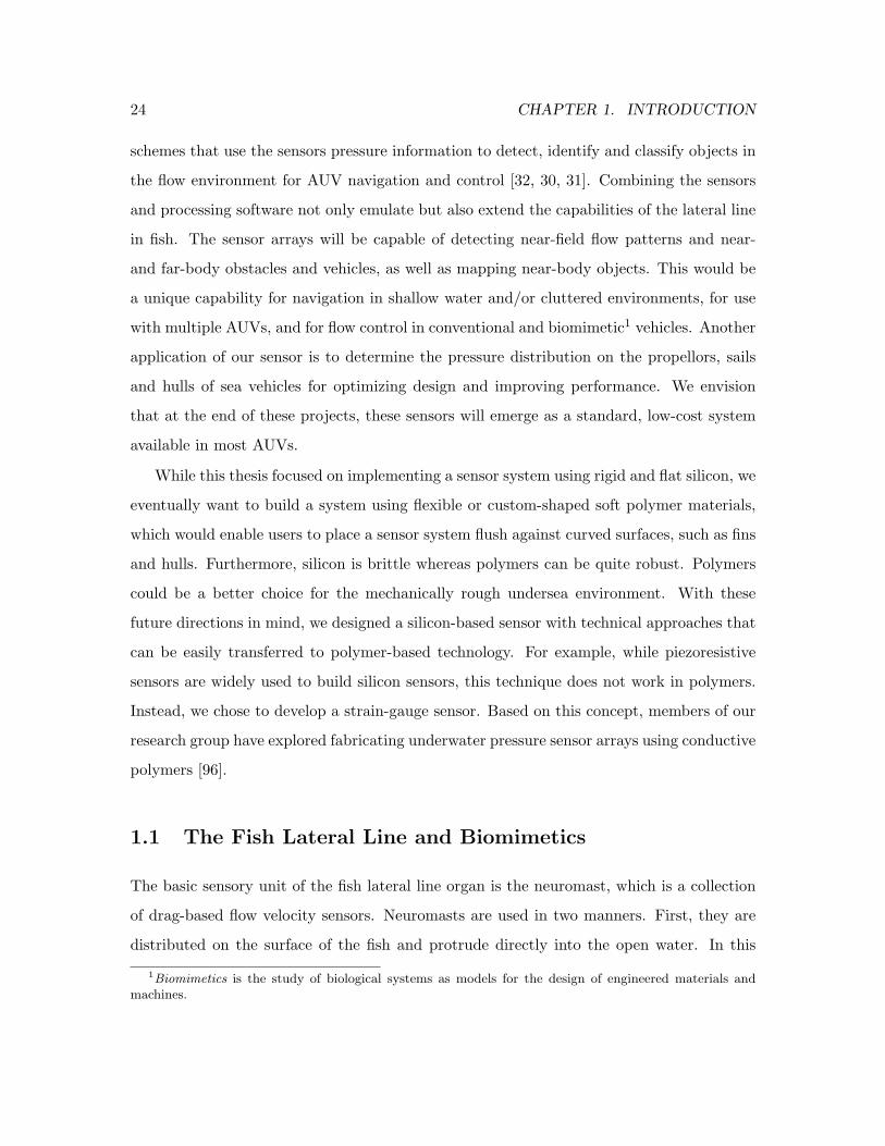
1-3 Typical locations for the lateral lines in fish. . . . . . . . . . . . . . . . . . . 25
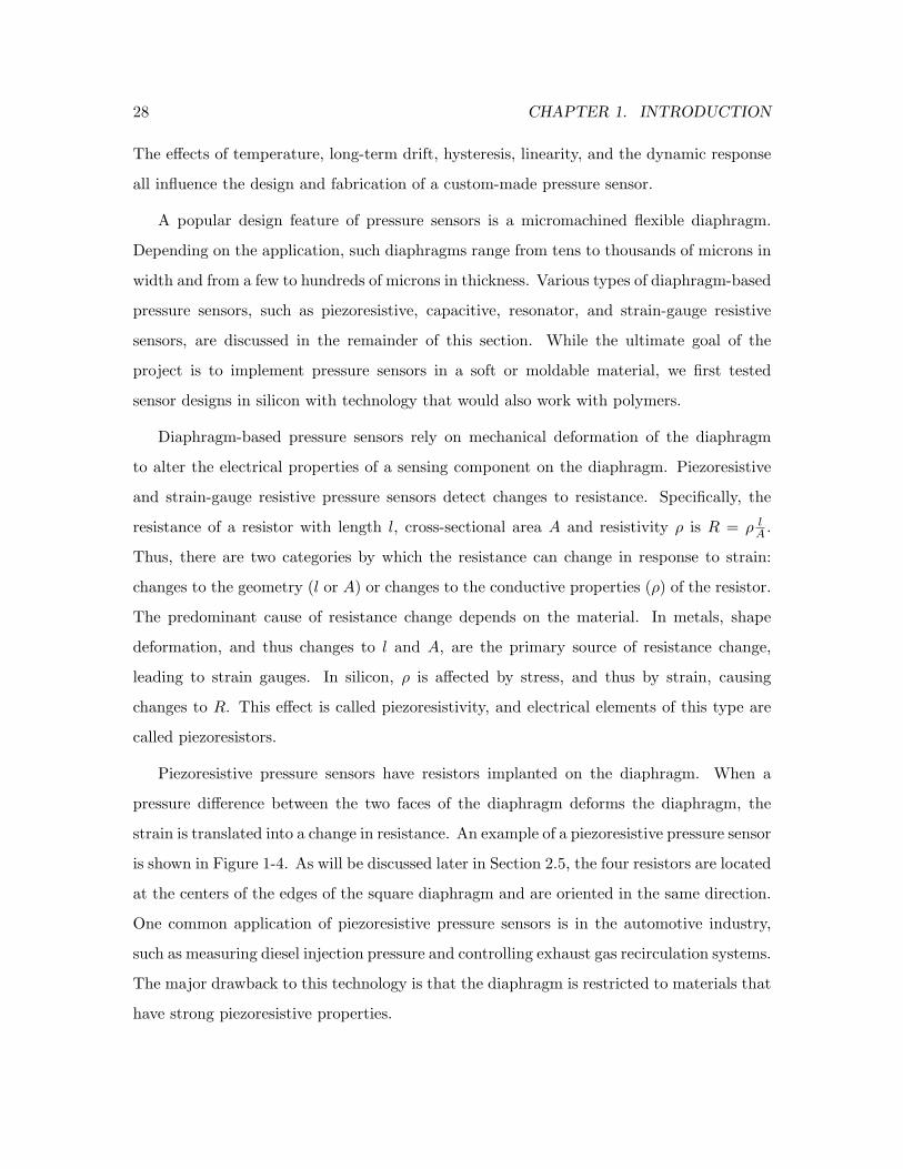
1-4 Cross-section and plan view of a typical bulk micromachined piezoresistive
pressure sensor. . . . . . . . . . . . . . . . . . . . . . . . . . . . . . . . . . . 29
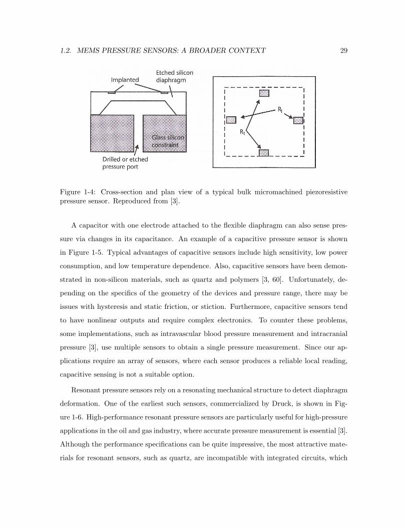
1-5 Cross-section of a typical silicon/Pyrex capacitive pressure sensor. . . . . . 30
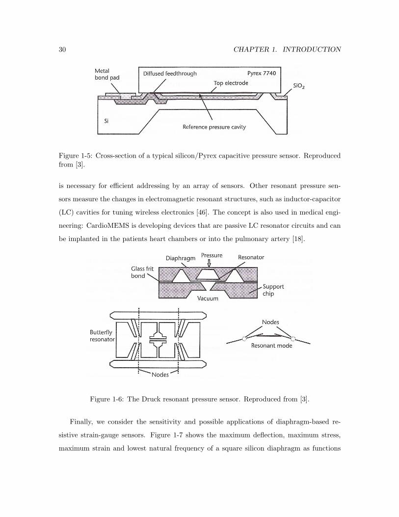
1-6 The Druck resonant pressure sensor. . . . . . . . . . . . . . . . . . . . . . . 30
1-7 Principal mechanical properties of a sensor as functions of diaphragm thick-
ness and length. . . . . . . . . . . . . . . . . . . . . . . . . . . . . . . . . . . 31
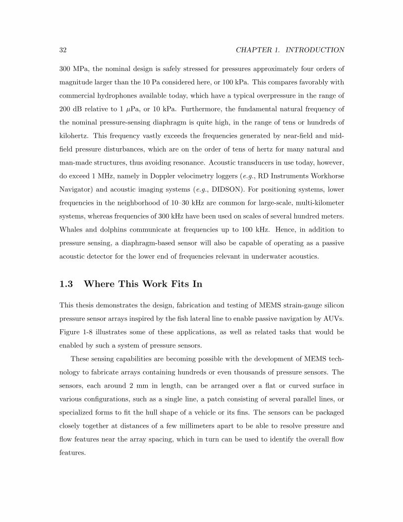
1-8 Four potential applications of the biomimetic pressure sensor array system. 33
2-1 Diagram of pressure-sensor array with basic structure depicted. . . . . . . . 40
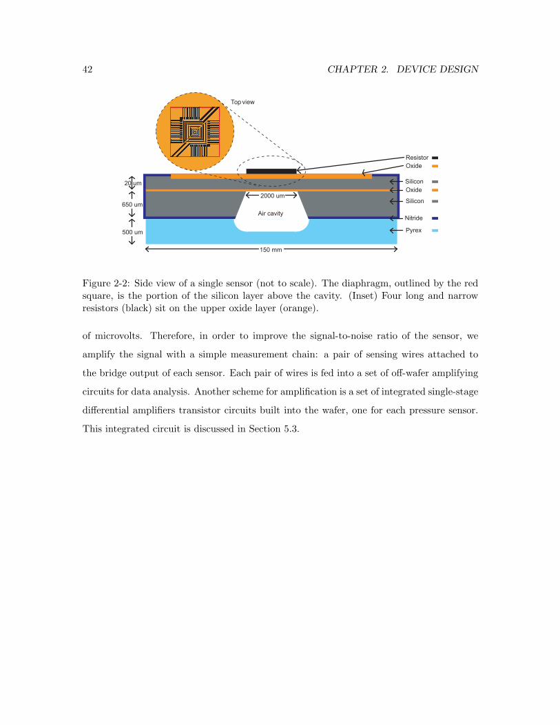
2-2 Side view of a single sensor. . . . . . . . . . . . . . . . . . . . . . . . . . . . 42
2-3 Schematic of air channels for underwater sensors. . . . . . . . . . . . . . . . 44
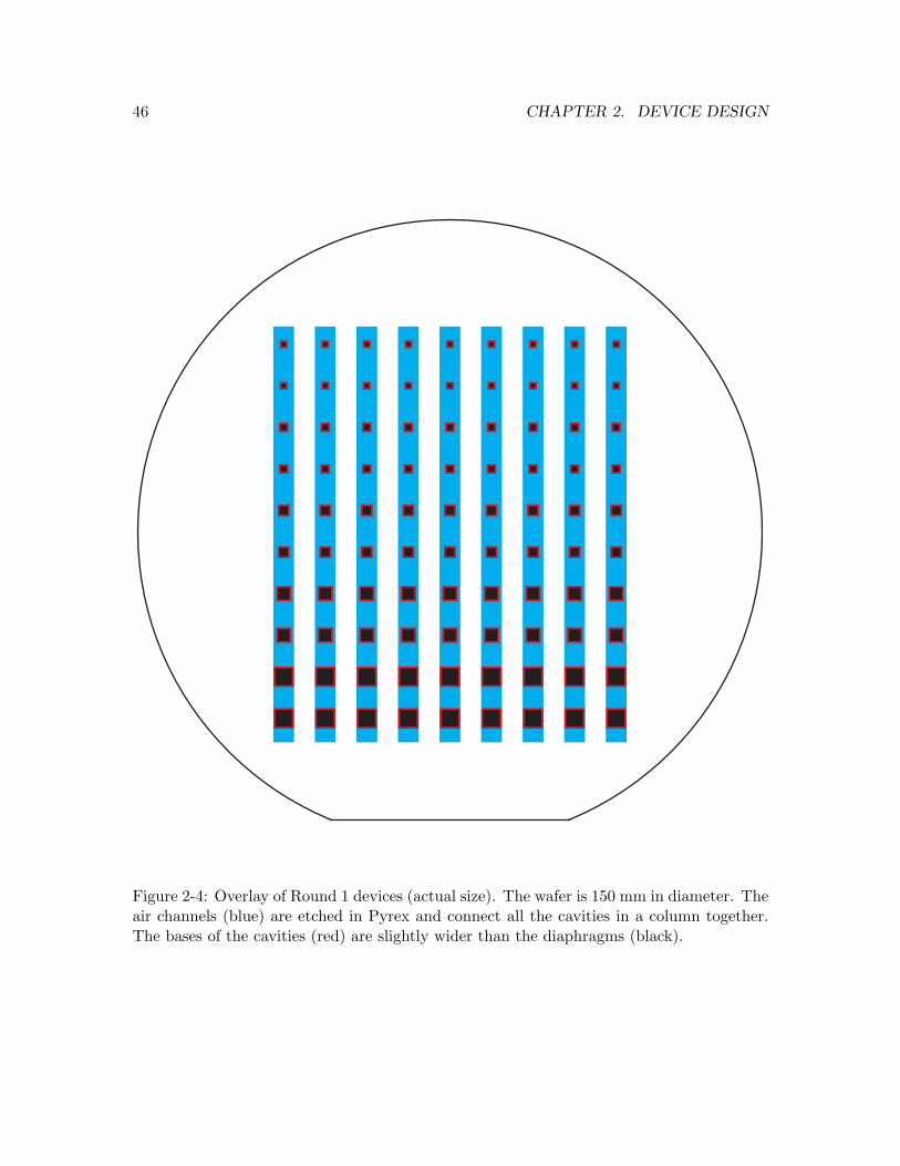
2-4 Overlay of Round 1 devices. . . . . . . . . . . . . . . . . . . . . . . . . . . . 46
2-5 Layout of resistors from Rounds 2 and 3. . . . . . . . . . . . . . . . . . . . . 47
2-6 Overlay of Round 3b devices. . . . . . . . . . . . . . . . . . . . . . . . . . . 49
2-7 Overlay of Round 4 devices. . . . . . . . . . . . . . . . . . . . . . . . . . . . 51
2-8 Crystal planes and major directions. . . . . . . . . . . . . . . . . . . . . . . 52
2-9 Crystal orientation in (100) silicon wafers. . . . . . . . . . . . . . . . . . . . 53
2-10 The Wheatstone bridge circuit. . . . . . . . . . . . . . . . . . . . . . . . . . 57
13

14 LIST OF FIGURES
2-11 Four resistors along a 〈110〉 direction at the centers of the four edges of the
surface of a square diaphragm. . . . . . . . . . . . . . . . . . . . . . . . . . 61
2-12 A square diaphragm of length L and thickness H. . . . . . . . . . . . . . . . 65
2-13 The strain of the top surface of the diaphragm in the x direction (ǫx) as a
function of normalized positions. . . . . . . . . . . . . . . . . . . . . . . . . 75
2-14 The local optimal resistor lengthwise orientation for maximizing resistance
change. . . . . . . . . . . . . . . . . . . . . . . . . . . . . . . . . . . . . . . 76
2-15 The sign of the resistance change when a local resistor is placed in the optimal
direction. . . . . . . . . . . . . . . . . . . . . . . . . . . . . . . . . . . . . . 77
2-16 The design of four strain-gauge resistors on a square diaphragm. . . . . . . 79
3-1 Standard photolithography. . . . . . . . . . . . . . . . . . . . . . . . . . . . 93
3-2 Mask-making process. . . . . . . . . . . . . . . . . . . . . . . . . . . . . . . 94
3-3 Examples of KOH-etching (100) silicon. . . . . . . . . . . . . . . . . . . . . 97
3-4 Side view of KOH wafer holder. . . . . . . . . . . . . . . . . . . . . . . . . . 100
3-5 Two-sided alignment mechanism. . . . . . . . . . . . . . . . . . . . . . . . . 118
3-6 Mask alignment marks. . . . . . . . . . . . . . . . . . . . . . . . . . . . . . 119
4-1 Device from Round 1 (silicon diaphragm without strain-gauge resistors). . . 122
4-2 An entire wafer from Round 2 (strain-gauge resistors on dummy nitride wafer).123
4-3 An entire wafer from Round 3 (isolated strain-gauge sensors). . . . . . . . . 124
4-4 An entire wafer from Round 4 (interconnected sensors). . . . . . . . . . . . 125
4-5 Manometer used to control the pressure in the cavities of devices from Rounds
1 and 3. . . . . . . . . . . . . . . . . . . . . . . . . . . . . . . . . . . . . . . 127
4-6 Photograph of the Zygo profilometer. . . . . . . . . . . . . . . . . . . . . . . 128
4-7 Circuit diagram of off-wafer differential amplifier. . . . . . . . . . . . . . . . 129
4-8 Static and frequency responses of off-wafer differential amplifiers. . . . . . . 130
4-9 Photograph of the head of the Tech-Etch cable. . . . . . . . . . . . . . . . . 131
4-10 Photograph of the water-level probe (sideways). . . . . . . . . . . . . . . . . 132
4-11 Voltage vs. pressure to calibrate the water-level probe. . . . . . . . . . . . . 133
LIST OF FIGURES 15
4-12 Profiles of a 2828 µm diaphragm at a pressure of −1500 Pa. . . . . . . . . . 134
4-13 Profiles of a 2828 µm diaphragm at a pressure of +1500 Pa. . . . . . . . . . 135
4-14 The deflection of the center of the diaphragm at various pressures for two
different sizes. . . . . . . . . . . . . . . . . . . . . . . . . . . . . . . . . . . . 139
4-15 The deflection of the center of the diaphragm at various pressures for a 4000
µm diaphragm. . . . . . . . . . . . . . . . . . . . . . . . . . . . . . . . . . . 140
4-16 Experimental set up for testing one strain-gauge resistor. . . . . . . . . . . 142
4-17 The amplified output of an external bridge testing a single resistor on a 4000
µm diaphragm over an 80-second period. . . . . . . . . . . . . . . . . . . . . 143
4-18 Contact resistance stabilized by regular epoxy and microscope probe needle
tips. . . . . . . . . . . . . . . . . . . . . . . . . . . . . . . . . . . . . . . . . 146
4-19 Contact resistance stabilized by WEST SYSTEM R© epoxy and microscope
probe needle tips. . . . . . . . . . . . . . . . . . . . . . . . . . . . . . . . . . 146
4-20 Contact resistance stabilized by both types of mechanical epoxies and micro-
scope probe needle tips. . . . . . . . . . . . . . . . . . . . . . . . . . . . . . 147
4-21 The output of an external bridge from a 4000 µm diaphragm undergoing
±1600 Pa changes. . . . . . . . . . . . . . . . . . . . . . . . . . . . . . . . . 149
4-22 The output of an external bridge from a 4000 µm diaphragm undergoing
±200 Pa changes. . . . . . . . . . . . . . . . . . . . . . . . . . . . . . . . . . 150
4-23 The output of an external bridge from a 4000 µm diaphragm undergoing a
200 Pa step. . . . . . . . . . . . . . . . . . . . . . . . . . . . . . . . . . . . . 151
4-24 External bridge voltage vs. pressure for various resistors from a 4000 µm
diaphragm. . . . . . . . . . . . . . . . . . . . . . . . . . . . . . . . . . . . . 152
4-25 External bridge voltage vs. pressure for various resistors from a 2828 µm
diaphragm. . . . . . . . . . . . . . . . . . . . . . . . . . . . . . . . . . . . . 153
4-26 External bridge voltage vs. pressure for various resistors from another 2828
µm diaphragm. . . . . . . . . . . . . . . . . . . . . . . . . . . . . . . . . . . 154
4-27 External bridge voltage vs. pressure for various resistors from a 2000 µm
diaphragm. . . . . . . . . . . . . . . . . . . . . . . . . . . . . . . . . . . . . 155

16 LIST OF FIGURES
4-28 External bridge voltage vs. pressure for various resistors from another 2000
µm diaphragm. . . . . . . . . . . . . . . . . . . . . . . . . . . . . . . . . . . 156
4-29 Photograph of a mounted wafer with pressure sensors that can be used un-
derwater (Round 4). . . . . . . . . . . . . . . . . . . . . . . . . . . . . . . . 159
4-30 Sample trace of two pressure sensors 2 cm apart (Round 4) activated by air
gun swiped across wafer. . . . . . . . . . . . . . . . . . . . . . . . . . . . . . 160
4-31 Bucket set up. . . . . . . . . . . . . . . . . . . . . . . . . . . . . . . . . . . . 161
4-32 Resonant bucket waves. . . . . . . . . . . . . . . . . . . . . . . . . . . . . . 162
5-1 Interconnect wiring of an array of pressure-sensing cells. . . . . . . . . . . . 172
5-2 Schematic of the integrated transistor amplifier and array read-out circuitry
for a 2 × 2 array. . . . . . . . . . . . . . . . . . . . . . . . . . . . . . . . . . 173
5-3 Layout of one cell of the integrated transistor amplifier and array read-out
circuit. . . . . . . . . . . . . . . . . . . . . . . . . . . . . . . . . . . . . . . . 174
5-4 Side view of the strain-gauge pressure sensor with integrated transistor am-
plifier and array read-out circuitry. . . . . . . . . . . . . . . . . . . . . . . . 175
5-5 Diagram and photograph of the elastomer-based pressure sensors described
in [96]. . . . . . . . . . . . . . . . . . . . . . . . . . . . . . . . . . . . . . . . 178
5-6 Diagram of the three-terminal squitch described in [64]. . . . . . . . . . . . 179
D-1 Mask P (Rounds 1 and 3a). . . . . . . . . . . . . . . . . . . . . . . . . . . . 210
D-2 Mask N (Rounds 1 and 3a). . . . . . . . . . . . . . . . . . . . . . . . . . . . 211
D-3 Mask M (Rounds 1 and 3a). . . . . . . . . . . . . . . . . . . . . . . . . . . . 212
D-4 Mask D (Round 1). . . . . . . . . . . . . . . . . . . . . . . . . . . . . . . . . 213
D-5 Mask R (Rounds 2, 3a and 3b). . . . . . . . . . . . . . . . . . . . . . . . . . 214
D-6 Mask D (Round 3a). . . . . . . . . . . . . . . . . . . . . . . . . . . . . . . . 215
D-7 Mask P (Round 3b). . . . . . . . . . . . . . . . . . . . . . . . . . . . . . . . 216
D-8 Mask O (Round 3b). . . . . . . . . . . . . . . . . . . . . . . . . . . . . . . . 217
D-9 Mask D (Round 3b). . . . . . . . . . . . . . . . . . . . . . . . . . . . . . . . 218
D-10Mask P (Round 4). . . . . . . . . . . . . . . . . . . . . . . . . . . . . . . . . 219

LIST OF FIGURES 17
D-11Mask O (Round 4). . . . . . . . . . . . . . . . . . . . . . . . . . . . . . . . . 220
D-12Mask D (Round 4). . . . . . . . . . . . . . . . . . . . . . . . . . . . . . . . . 221
D-13Mask R (Round 4). . . . . . . . . . . . . . . . . . . . . . . . . . . . . . . . . 222
E-1 KOH wafer holder: bottom view of bottom piece. . . . . . . . . . . . . . . . 224
E-2 KOH wafer holder: bottom view of top piece. . . . . . . . . . . . . . . . . . 225
E-3 KOH wafer holder: top view of top piece. . . . . . . . . . . . . . . . . . . . 226
E-4 Tech-Etch cable. . . . . . . . . . . . . . . . . . . . . . . . . . . . . . . . . . 227

18 LIST OF FIGURES

List of Tables
2.1 Piezoresistive coefficients along a 〈110〉 direction for both types of doped silicon. 60
2.2 Expected performance parameters for strain-gauge pressure sensors of various
diaphragm lengths L. . . . . . . . . . . . . . . . . . . . . . . . . . . . . . . . 84
3.1 Variations on fabrication for Rounds 1, 2, 3a, 3b and 4. . . . . . . . . . . . 91
3.2 Diagram of cross-sectional trench profiles from different types of etch methods. 95
3.3 Process flow for etching Pyrex wafers. . . . . . . . . . . . . . . . . . . . . . 104
4.1 Slopes c1/P for various diaphragm lengths L. . . . . . . . . . . . . . . . . . 136
4.2 Experimental values of slopes of best-fit lines for amplified voltage vs. pres-
sure for strain-gauge resistors on various diaphragms from Round 3b. . . . . 157
4.3 Theoretical values of slopes of best-fit lines for amplified voltage vs. pressure
for strain-gauge resistors on various diaphragms from Round 3b. . . . . . . 157
A.1 Chemical formulas and full names. . . . . . . . . . . . . . . . . . . . . . . . 181
B.1 Recipe for bonding silicon and Pyrex. . . . . . . . . . . . . . . . . . . . . . 195
C.1 Process flow for standard single-sided photolithography. . . . . . . . . . . . 198
C.2 Process flow for standard double-sided photolithography. . . . . . . . . . . . 198
C.3 Process flow for finding the crystalline plane for (100) silicon. . . . . . . . . 199
C.4 Process flow for Pyrex wafers for strain-gauge silicon sensors without tran-
sistors. . . . . . . . . . . . . . . . . . . . . . . . . . . . . . . . . . . . . . . . 201
C.5 Process flow for SOI wafers for strain-gauge silicon sensors without transistors.201
19

20 LIST OF TABLES
C.6 Process flow for SOI wafers for strain-gauge silicon sensors without transistors
(cont.). . . . . . . . . . . . . . . . . . . . . . . . . . . . . . . . . . . . . . . . 202
C.7 Remainder of process flow for strain-gauge silicon sensors without transistors. 203
C.8 Process flow for Pyrex wafers for strain-gauge silicon sensors with transistors. 205
C.9 Process flow for SOI wafers for strain-gauge silicon sensors with transistors. 206
C.10 Process flow for SOI wafers for strain-gauge silicon sensors with transistors
(cont.). . . . . . . . . . . . . . . . . . . . . . . . . . . . . . . . . . . . . . . . 207
C.11 Process flow for SOI wafers for strain-gauge silicon sensors with transistors
(conc.). . . . . . . . . . . . . . . . . . . . . . . . . . . . . . . . . . . . . . . 207
C.12 Remainder of process flow for strain-gauge silicon sensors with transistors. . 208
D.1 List of masks used for each round of devices. . . . . . . . . . . . . . . . . . 209
Chapter 1
Introduction
Many methods of sensing have been used by undersea vehicles to obtain three-dimensional
mappings of the surrounding ocean floor, walls and other objects. Such maps aid vehicles
in navigating through unfamiliar territory, avoiding collisions with moving objects, and
surveilling the environment. The most common methods–sonar, radar and optical sensing–
require active transceivers and thus use significant amounts of power. For small autonomous
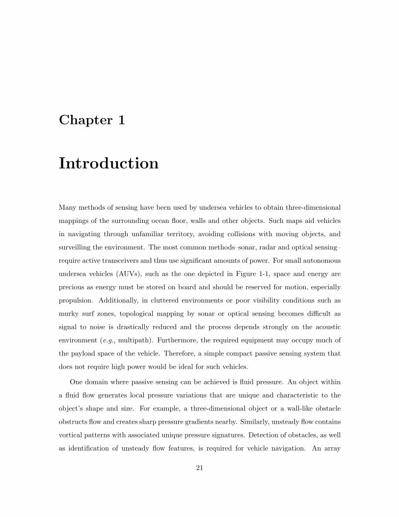
undersea vehicles (AUVs), such as the one depicted in Figure 1-1, space and energy are
precious as energy must be stored on board and should be reserved for motion, especially
propulsion. Additionally, in cluttered environments or poor visibility conditions such as
murky surf zones, topological mapping by sonar or optical sensing becomes difficult as
signal to noise is drastically reduced and the process depends strongly on the acoustic
environment (e.g., multipath). Furthermore, the required equipment may occupy much of
the payload space of the vehicle. Therefore, a simple compact passive sensing system that
does not require high power would be ideal for such vehicles.
One domain where passive sensing can be achieved is fluid pressure. An object within
a fluid flow generates local pressure variations that are unique and characteristic to the
object’s shape and size. For example, a three-dimensional object or a wall-like obstacle
obstructs flow and creates sharp pressure gradients nearby. Similarly, unsteady flow contains
vortical patterns with associated unique pressure signatures. Detection of obstacles, as well
as identification of unsteady flow features, is required for vehicle navigation. An array
21
22 CHAPTER 1. INTRODUCTION
Figure 1-1: Finnegan the RoboTurtle, an MIT-developed biomimetic autonomous underseavehicle (AUV), navigating in a swimming pool.
of passive underwater pressure sensors, with their ability to “touch at a distance” with
minimal power consumption, would be able to resolve the pressure signatures of obstacles
in the near field and the wake of objects in the intermediate field. As an additional benefit,
with proper design, pressure sensors can also be used to sample acoustic signals as well.
Fish already have a biological version of such a pressure sensor system, namely the
lateral line organ, and this thesis is inspired by their approach. The blind Mexican cavefish,
Astyanax fasciatus, can form full real-time three-dimensional maps of its surroundings to
move in unfamiliar environments at high speeds without collisions [59, 89]. Unlike the
electrolocation sense found in some species of fish, A. fasciatus accomplishes this surprising
feat without the use of electric fields, and instead relies primarily on its lateral line organ.
While all fish have this organ, not all use it to the extent that the blind cavefish does [59].
The lateral line is a spatially-distributed set of sensors over a fish’s body that allows the fish
to monitor its hydrodynamic environment, influenced by external disturbances. Through its
ability to resolve pressure signatures of objects, the fish obtains “hydrodynamic pictures”,
enabling the lateral line to act like a “touch at a distance” device.
Many other lateral-line-mediated behaviors in fish have been identified by biologists
[67, 89], including (a) rheotaxis, or orienting themselves to currents and holding stationary in
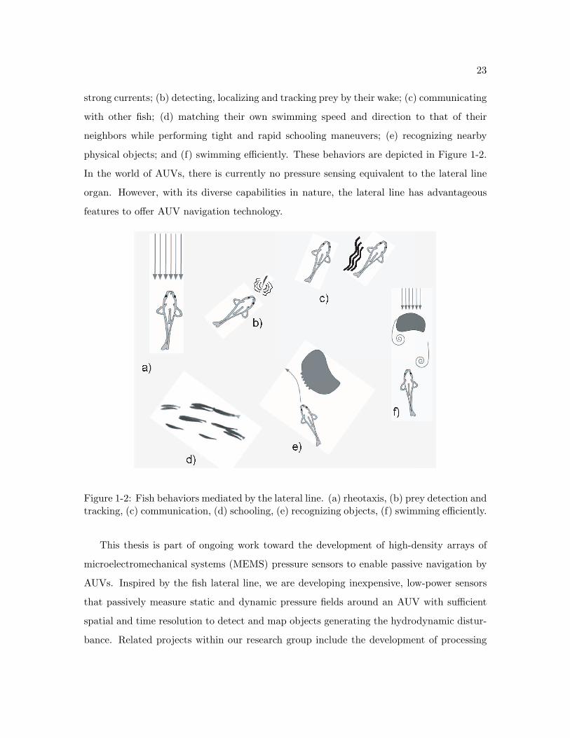
23
strong currents; (b) detecting, localizing and tracking prey by their wake; (c) communicating
with other fish; (d) matching their own swimming speed and direction to that of their
neighbors while performing tight and rapid schooling maneuvers; (e) recognizing nearby
physical objects; and (f) swimming efficiently. These behaviors are depicted in Figure 1-2.
In the world of AUVs, there is currently no pressure sensing equivalent to the lateral line
organ. However, with its diverse capabilities in nature, the lateral line has advantageous
features to offer AUV navigation technology.
Figure 1-2: Fish behaviors mediated by the lateral line. (a) rheotaxis, (b) prey detection andtracking, (c) communication, (d) schooling, (e) recognizing objects, (f) swimming efficiently.
This thesis is part of ongoing work toward the development of high-density arrays of
microelectromechanical systems (MEMS) pressure sensors to enable passive navigation by
AUVs. Inspired by the fish lateral line, we are developing inexpensive, low-power sensors
that passively measure static and dynamic pressure fields around an AUV with sufficient
spatial and time resolution to detect and map objects generating the hydrodynamic distur-
bance. Related projects within our research group include the development of processing
24 CHAPTER 1. INTRODUCTION
schemes that use the sensors pressure information to detect, identify and classify objects in
the flow environment for AUV navigation and control [32, 30, 31]. Combining the sensors
and processing software not only emulate but also extend the capabilities of the lateral line
in fish. The sensor arrays will be capable of detecting near-field flow patterns and near-
and far-body obstacles and vehicles, as well as mapping near-body objects. This would be
a unique capability for navigation in shallow water and/or cluttered environments, for use
with multiple AUVs, and for flow control in conventional and biomimetic1 vehicles. Another
application of our sensor is to determine the pressure distribution on the propellors, sails
and hulls of sea vehicles for optimizing design and improving performance. We envision
that at the end of these projects, these sensors will emerge as a standard, low-cost system
available in most AUVs.
While this thesis focused on implementing a sensor system using rigid and flat silicon, we
eventually want to build a system using flexible or custom-shaped soft polymer materials,
which would enable users to place a sensor system flush against curved surfaces, such as fins
and hulls. Furthermore, silicon is brittle whereas polymers can be quite robust. Polymers
could be a better choice for the mechanically rough undersea environment. With these
future directions in mind, we designed a silicon-based sensor with technical approaches that
can be easily transferred to polymer-based technology. For example, while piezoresistive
sensors are widely used to build silicon sensors, this technique does not work in polymers.
Instead, we chose to develop a strain-gauge sensor. Based on this concept, members of our
research group have explored fabricating underwater pressure sensor arrays using conductive
polymers [96].
1.1 The Fish Lateral Line and Biomimetics
The basic sensory unit of the fish lateral line organ is the neuromast, which is a collection
of drag-based flow velocity sensors. Neuromasts are used in two manners. First, they are
distributed on the surface of the fish and protrude directly into the open water. In this
1Biomimetics is the study of biological systems as models for the design of engineered materials andmachines.
1.1. THE FISH LATERAL LINE AND BIOMIMETICS 25
Figure 1-3: Typical locations for the lateral lines in fish (red). Reproduced from [34].
arrangement, the neuromasts are directly stimulated by the local fluid velocity to sense
flow. As shown in Figure 1-3, the specific distribution of neuromasts varies widely from
species to species. Second, the neuromasts are enclosed in canals with pores that open to
the outside flow periodically [34]. These canals have been described as an array of pressure
gradient sensors [20], where a pressure difference between adjacent pores drives fluid motion
in the canal, and thereby stimulates the neuromasts. Studies that selectively deactivated
the canals found that the mapping abilities of the lateral line appear to be predominantly
accomplished by its canal system [59]. By measuring the pressure gradient as a function of
location along the fish’s body and time, the fish is able to locate and identify nearby objects
as well as determine their shapes and velocities.
While the lateral line organ cannot be identically implemented with standard fabrication
technologies, the capabilities similar to that of the lateral line would greatly benefit AUVs.
In particular, the ability to locate and obtain information about nearby obstructions is
increasingly important as AUVs are finding applications in cluttered environments and surf
zones. Also, the ability for flow mapping and identifying vortical structures allows the
possibility for optimizing control and navigation in unsteady environments. In addition to
26 CHAPTER 1. INTRODUCTION
these capabilities, a distributed pressure sensor system would be completely passive and
consequently require little power. Compared to active systems like sonar, the primary
disadvantage of a pressure sensor system would be its limited range, or the maximum
distance of detected objects.
A number of researchers have experimentally and numerically studied the fish’s lateral
line and its ability to identify objects and flow structures. In investigating the blind fish’s
object sensing skills, [89] constructed a model neuromast and demonstrated the neuromast’s
ability to locate plates and thin beams at a distance of 2 mm. [40, 41] measured the dynamic
pressure distributions generated on the body of a model fish when gliding alongside and into
a wall at similar millimeter-scale distances. [87] showed that goldfish use their lateral line to
detect and discriminate the size, velocity and shape of passing rods in still water. Numerical
experiments by [79] demonstrated that an array of pressure sensors could track the position
and circulation in a channel. While free stream flows are more complex and unpredictable
in open water than single vortices are, [79] established that an array of pressure sensors is a
viable way to identify and track vortices. The question remains how well a simple pressure
sensor array is able to distinguish between moving objects of different shapes and sizes.
Our group has used commercial pressure sensors separated on the order of 10 millimeters
to record pressure signals resulting from flow around both still and moving objects. Using
principal component analysis (PCA) and Kalman filtering on the recorded signals, we could
discriminate between various cylindrical objects with round and square cross-sections of sizes
on the order of several centimeters. Similarly, we could track motion up to half a meter
per second using commercial pressure sensors separated on the order of several millimeters
apart. We found that a classification error rate of under 2% can be achieved with a 2
kPa range, 10 Pa resolution, and 60 Hz data acquisition rate [30, 31, 23]. The pressure
sensor spacing would need to be on the order of millimeters in order to capture the relevant
features in a single instance, which would be necessary under non-uniform conditions found
outside laboratory conditions.
1.2. MEMS PRESSURE SENSORS: A BROADER CONTEXT 27
1.2 MEMS Pressure Sensors: A Broader Context
Microelectromechanical systems (MEMS)2 are micro-scale devices that enable the operation
of complex systems by converting physical stimuli from the mechanical, thermal, chemical
and optical domains to the electrical domain. MEMS engineers engage technologies across
a wide set of scientific disciplines, including physics, chemistry, material science, integrated
circuit (IC) fabrication and manufacturing. Due to its origins from the IC industry, much of
MEMS technology is based on silicon, the substrate material used for the vast majority of
commercial electronics. However, there is ongoing research in other materials as well, such
as plastics and ceramics, for their lower costs and biocompatibility for medical applications.
As a result of its interdisciplinary nature, MEMS technology has found use in many
industries, especially automotive, medical and aerospace. A device class where MEMS have
thrived is sensing. For example, early crash sensors for airbag safety systems were merely
mechanical switches. Today, airbag systems use MEMS sensors that not only measure
acceleration, but also provide self-diagnostics and integration with other sensors in the
vehicle. Other types of MEMS sensors currently undergoing rapid research progress include
flow sensing for biomedical applications [3], microphones for portable devices [72], and
accelerometers for touch screens and gaming [35, 69].
After accelerators, pressure sensors are the most commercially successful class of MEMS
sensors. These devices employ a broad range of techniques to convert mechanical pressure
into electrical signals, such as piezoresistive, capacitive, resonant, and strain-gauge resistive
sensing. Furthermore, the list of applications of pressure sensors has also grown tremen-
dously over the past three decades. As a result, pressure sensing has developed into a
market where highly specialized devices can be found for specific needs. The fundamental
specification of a pressure sensor is its operating pressure range. Other obvious parame-
ters, such as physical dimensions, pressure resolution, reliability, lifespan, environmental
compatibility and cost are also important, but there are more subtle considerations as well.
2Microelectromechanical systems is the term most commonly used in the United States. In Europe, thetechnology is generally known as microsystems technology (MST), whereas in Japan, the term micromachinesis used in English-language publications. This thesis follows the U.S. convention.
28 CHAPTER 1. INTRODUCTION
The effects of temperature, long-term drift, hysteresis, linearity, and the dynamic response
all influence the design and fabrication of a custom-made pressure sensor.
A popular design feature of pressure sensors is a micromachined flexible diaphragm.
Depending on the application, such diaphragms range from tens to thousands of microns in
width and from a few to hundreds of microns in thickness. Various types of diaphragm-based
pressure sensors, such as piezoresistive, capacitive, resonator, and strain-gauge resistive
sensors, are discussed in the remainder of this section. While the ultimate goal of the
project is to implement pressure sensors in a soft or moldable material, we first tested
sensor designs in silicon with technology that would also work with polymers.
Diaphragm-based pressure sensors rely on mechanical deformation of the diaphragm
to alter the electrical properties of a sensing component on the diaphragm. Piezoresistive
and strain-gauge resistive pressure sensors detect changes to resistance. Specifically, the
resistance of a resistor with length l, cross-sectional area A and resistivity ρ is R = ρ lA.
Thus, there are two categories by which the resistance can change in response to strain:
changes to the geometry (l or A) or changes to the conductive properties (ρ) of the resistor.
The predominant cause of resistance change depends on the material. In metals, shape
deformation, and thus changes to l and A, are the primary source of resistance change,
leading to strain gauges. In silicon, ρ is affected by stress, and thus by strain, causing
changes to R. This effect is called piezoresistivity, and electrical elements of this type are
called piezoresistors.
Piezoresistive pressure sensors have resistors implanted on the diaphragm. When a
pressure difference between the two faces of the diaphragm deforms the diaphragm, the
strain is translated into a change in resistance. An example of a piezoresistive pressure sensor
is shown in Figure 1-4. As will be discussed later in Section 2.5, the four resistors are located
at the centers of the edges of the square diaphragm and are oriented in the same direction.
One common application of piezoresistive pressure sensors is in the automotive industry,
such as measuring diesel injection pressure and controlling exhaust gas recirculation systems.
The major drawback to this technology is that the diaphragm is restricted to materials that
have strong piezoresistive properties.
1.2. MEMS PRESSURE SENSORS: A BROADER CONTEXT 29
Figure 1-4: Cross-section and plan view of a typical bulk micromachined piezoresistivepressure sensor. Reproduced from [3].
A capacitor with one electrode attached to the flexible diaphragm can also sense pres-
sure via changes in its capacitance. An example of a capacitive pressure sensor is shown
in Figure 1-5. Typical advantages of capacitive sensors include high sensitivity, low power
consumption, and low temperature dependence. Also, capacitive sensors have been demon-
strated in non-silicon materials, such as quartz and polymers [3, 60]. Unfortunately, de-
pending on the specifics of the geometry of the devices and pressure range, there may be
issues with hysteresis and static friction, or stiction. Furthermore, capacitive sensors tend
to have nonlinear outputs and require complex electronics. To counter these problems,
some implementations, such as intravascular blood pressure measurement and intracranial
pressure [3], use multiple sensors to obtain a single pressure measurement. Since our ap-
plications require an array of sensors, where each sensor produces a reliable local reading,
capacitive sensing is not a suitable option.
Resonant pressure sensors rely on a resonating mechanical structure to detect diaphragm
deformation. One of the earliest such sensors, commercialized by Druck, is shown in Fig-
ure 1-6. High-performance resonant pressure sensors are particularly useful for high-pressure
applications in the oil and gas industry, where accurate pressure measurement is essential [3].
Although the performance specifications can be quite impressive, the most attractive mate-
rials for resonant sensors, such as quartz, are incompatible with integrated circuits, which
30 CHAPTER 1. INTRODUCTION
Figure 1-5: Cross-section of a typical silicon/Pyrex capacitive pressure sensor. Reproducedfrom [3].
is necessary for efficient addressing by an array of sensors. Other resonant pressure sen-
sors measure the changes in electromagnetic resonant structures, such as inductor-capacitor
(LC) cavities for tuning wireless electronics [46]. The concept is also used in medical engi-
neering: CardioMEMS is developing devices that are passive LC resonator circuits and can
be implanted in the patients heart chambers or into the pulmonary artery [18].
Figure 1-6: The Druck resonant pressure sensor. Reproduced from [3].
Finally, we consider the sensitivity and possible applications of diaphragm-based re-
sistive strain-gauge sensors. Figure 1-7 shows the maximum deflection, maximum stress,
maximum strain and lowest natural frequency of a square silicon diaphragm as functions
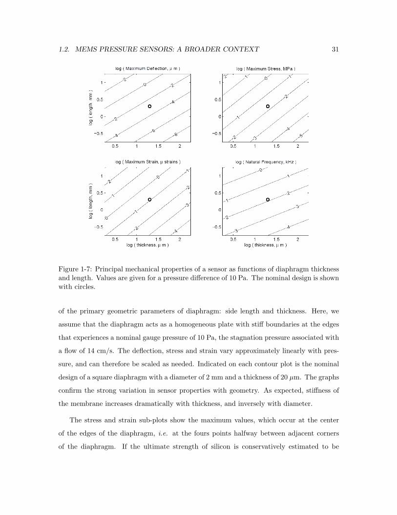
1.2. MEMS PRESSURE SENSORS: A BROADER CONTEXT 31
Figure 1-7: Principal mechanical properties of a sensor as functions of diaphragm thicknessand length. Values are given for a pressure difference of 10 Pa. The nominal design is shownwith circles.
of the primary geometric parameters of diaphragm: side length and thickness. Here, we
assume that the diaphragm acts as a homogeneous plate with stiff boundaries at the edges
that experiences a nominal gauge pressure of 10 Pa, the stagnation pressure associated with
a flow of 14 cm/s. The deflection, stress and strain vary approximately linearly with pres-
sure, and can therefore be scaled as needed. Indicated on each contour plot is the nominal
design of a square diaphragm with a diameter of 2 mm and a thickness of 20 µm. The graphs
confirm the strong variation in sensor properties with geometry. As expected, stiffness of
the membrane increases dramatically with thickness, and inversely with diameter.
The stress and strain sub-plots show the maximum values, which occur at the center
of the edges of the diaphragm, i.e. at the fours points halfway between adjacent corners
of the diaphragm. If the ultimate strength of silicon is conservatively estimated to be
32 CHAPTER 1. INTRODUCTION
300 MPa, the nominal design is safely stressed for pressures approximately four orders of
magnitude larger than the 10 Pa considered here, or 100 kPa. This compares favorably with
commercial hydrophones available today, which have a typical overpressure in the range of
200 dB relative to 1 µPa, or 10 kPa. Furthermore, the fundamental natural frequency of
the nominal pressure-sensing diaphragm is quite high, in the range of tens or hundreds of
kilohertz. This frequency vastly exceeds the frequencies generated by near-field and mid-
field pressure disturbances, which are on the order of tens of hertz for many natural and
man-made structures, thus avoiding resonance. Acoustic transducers in use today, however,
do exceed 1 MHz, namely in Doppler velocimetry loggers (e.g., RD Instruments Workhorse
Navigator) and acoustic imaging systems (e.g., DIDSON). For positioning systems, lower
frequencies in the neighborhood of 10–30 kHz are common for large-scale, multi-kilometer
systems, whereas frequencies of 300 kHz have been used on scales of several hundred meters.
Whales and dolphins communicate at frequencies up to 100 kHz. Hence, in addition to
pressure sensing, a diaphragm-based sensor will also be capable of operating as a passive
acoustic detector for the lower end of frequencies relevant in underwater acoustics.
1.3 Where This Work Fits In
This thesis demonstrates the design, fabrication and testing of MEMS strain-gauge silicon
pressure sensor arrays inspired by the fish lateral line to enable passive navigation by AUVs.
Figure 1-8 illustrates some of these applications, as well as related tasks that would be
enabled by such a system of pressure sensors.
These sensing capabilities are becoming possible with the development of MEMS tech-
nology to fabricate arrays containing hundreds or even thousands of pressure sensors. The
sensors, each around 2 mm in length, can be arranged over a flat or curved surface in
various configurations, such as a single line, a patch consisting of several parallel lines, or
specialized forms to fit the hull shape of a vehicle or its fins. The sensors can be packaged
closely together at distances of a few millimeters apart to be able to resolve pressure and
flow features near the array spacing, which in turn can be used to identify the overall flow
features.
1.3. WHERE THIS WORK FITS IN 33
Figure 1-8: Four potential applications of the biomimetic pressure sensor array system.
Both self-propelled vehicles and obstacles standing within a smooth or turbulent current
generate flow disturbances. The near-field of this hydrodynamic disturbance extends typ-
ically about one body length around the generating object and is characterized by strong
pressure and velocity variations. Such near-body pressure variations are referred to as
“pseudo-sound” and can be detected by a sensor which is close to the obstacle. If the
disturbance is unsteady and its frequency is sufficiently high, the disturbances generates
acoustical waves that create a far-field disturbance, which is detectable at hundreds or
thousands of body lengths away, depending on the frequency. In addition, a hydrodynamic
wake is shed by the body and is detectable directly downstream from the generating body
as pressure and velocity fluctuations in the near and intermediate field, up to hundreds of
meters away from the source. The sensors we developed are appropriate to all three of these
regimes: pseudo-sound, high-frequency sound, and wakes, although we focused primarily on
applications for pseudo-sound and wake flows. For some standard objects, hydrodynamic
signatures and flow patterns are codified, so that the sensor system could potentially au-

34 CHAPTER 1. INTRODUCTION
tomatically detect objects and flow patterns. Our pressure sensor arrays can thus provide
the following capabilities to AUVs:
1. Measure the distance to the near-field objects, obstacles and other vehicles.
2. Determine the location, speed, direction and size of moving vehicles and objects.
3. Form accurate topological maps of nearby objects through reconstruction of their
shapes from predetermined pressure hydrodynamic signatures.
4. Assist maneuvering in cluttered environments in the presence of turbidity and turbu-
lence, and operations in the dark.
5. Assist in the coordination of multiple robots. Each robot vehicle will be provided at
low power with effective images of the location and orientation of the near-by vehicles.
6. Identify flow patterns in the surrounding flow to optimize fin and propulsor perfor-
mance. This flow information can also be used for energy extraction in biomimetic
vehicles.
Other sensing technologies, such as sonar or radar, also use arrays sometimes, but these
are limited to a few dozen in number and are centimeters or meters apart. The concept de-
scribed in this thesis can be scaled to an array of several hundred of sensors, each millimeters
apart.
This project is of interest not only to undersea researchers but also to the MEMS com-
munity as well. Currently, much of MEMS sensor development is focused on designing
single, extremely sensitive sensors for use in applications such as microphones [72]. Fur-
thermore, research in sensor arrays tends to be motivated by tactile applications [78]. From
the materials science perspective, undersea navigation provides motivation for MEMS re-
search in flexible, non-silicon substrates. Finally, by successfully demonstrating an array of
pressure sensors for undersea object identification, we hope the project will inspire further
work in integrating MEMS with macro-scale systems for high-precision applications.
1.4. PROJECT SUMMARY 35
1.4 Project Summary
A MEMS pressure sensor system based on strain gauges bonded to silicon diaphragms was
fabricated and tested. The system consists of a set of sensor cells spaced a few millimeters
apart fabricated on etched silicon and Pyrex wafers. Silicon and Pyrex are well-understood
MEMS substrates that provide a foundation for evaluating the feasibility of transferring our
pressure sensor design to polymer substrates. The sensing element on each cell is a set of
strain-gauge resistors mounted on a flexible 2-mm wide square diaphragm, which is a thin
20-µm layer of silicon attached at the edges to a square silicon cavity. The physical and
electrical dimensions of the sensor components were chosen to satisfy the sensitivity and
density specifications of the underwater environment. Finally, the sensors are attached to
an array read-out system with sufficient voltage and time resolution to enable data output
to a computer for further signal processing.
Several challenges were encountered in this project: read-out of an array of data, elec-
tronics for signal-to-noise enhancement, mechanical robustness, the equilibration of the back
pressure, dynamics and noise, and compatibility with polymers.
In order to develop a fully functional system ready for open water sensing and naviga-
tion, we modularly tested individual aspects of the sensor system under highly controlled
environments. However, all tests required the ability to read the array data. Thus, the
ability to collect the outputs from the sensor array accurately and at a high data rate (kHz
range) was of highest priority. As a first-pass solution, we have a pair of wires coming out
of each sensor cell to a standard wire bundle that is fed into a computer. While this is
acceptable for a small number of cells (fewer than 50), it is not easily scalable to hundreds
or thousands of cells. One scalable solution is inspired by magnetic core memory: with
transistor circuits connected to each sensor cell, signals address a particular column of cells,
and the output signals from the entire column is returned. This reduces the output wiring
to only a few fixed wires. However, while these electronics are conceptually simple, which is
critical for moving the sensor design to soft substrates, reliable fabrication and calibration
are significant challenges.
36 CHAPTER 1. INTRODUCTION
Since the undersea environment can be physically and chemically harsh, we designed the
sensor system to be robust against possible damages. The design includes safety mechanisms
that ensure that the loss of one cell will not affect the operation of the others. Of course,
there are trade-offs between simplicity and robustness. We chose and fabricated a reasonable
design that allowed us to test the system under controlled environments. In the future, we
plan to develop a system that is able to handle more realistic situations but would require
more complex electronics or layers of fabrication steps.
Another challenge is the equilibration of back pressure, which is pressure applied to the
back-side of the diaphragms from within the sensor cavity. To reliably map flow velocities in
the ocean, we are interested in detecting small-scale pressure fluctuations on the order of a
few pascals. However, large-scale homogeneous pressure changes, such as those experienced
when the entire system moves up or down relative to sea level would overwhelm any relevant
signal.3 Furthermore, the sensors are physically limited in their dynamic range. Diaphragm-
based sensors with sensitivity in the pascal range are not able to withstand pressures on
the order of 105 Pa without physically breaking or leading to permanent damage. To
design a robust sensor with good signal-to-noise, we remove the large-scale DC component
of pressure change via a common back pressure. We designed fluidic channels that enable
fast equilibration of the the back pressure so that our sensors are only detecting spatially
varying pressure gradients.
This thesis describes the design, fabrication and static testing of individual MEMS
strain-gauge silicon pressure sensors with amplification circuitry off-wafer. The results
demonstrate that the proposed technology is feasible for the underwater object detection
application described earlier. Remaining issues, including integrated amplifying and array-
processing circuitry, dynamic responses, and full array testing underwater are left as future
work.
3One meter of water creates approximately 10 kPa, or about 0.1 atm, of large-signal pressure.
1.5. THESIS ORGANIZATION 37
1.5 Thesis Organization
This chapter, Chapter 1, explains the motivation, background and objectives of the the-
sis. Chapter 2 describes the design of the strain-gauge pressure sensor system. Chapter 3
explains the fabrication design of the device, including wafer etching, photolithography, pro-
cess flow design and mask design. Chapter 4 contains the device measurements. Chapter 5
summarizes the work presented, conclusions drawn from the project, and suggestions for
future directions.
There are several appendices that provide more detailed information relevant to the main
text. Appendix A lists chemical formulas for common names and abbreviations used in this
thesis. Appendix B contains standard operating procedures during fabrication. Appendix C
contains full device process flows. Appendix D shows the masks used during fabrication.
Appendix E contains technical diagrams of the various apparatus used in fabrication and
measurement. Appendix F contains the MATLAB codes used for design analysis.
Finally, a list of reference materials is provided at the end of this thesis.

38 CHAPTER 1. INTRODUCTION
Chapter 2
Device Design
This chapter discusses the design of the strain-gauge pressure sensor system. Section 2.1
provides an overview of the device features. Section 2.2 describes the wafer-level features of
the various pressure sensor systems fabricated. Section 2.3 describes the properties of silicon
relevant for modeling device behavior and designing the fabrication process. Section 2.4
calculates the change in the output voltage of a Wheatstone bridge resulting from small
changes in the sense resistances. Section 2.5 discusses a well-known pressure sensor based
on piezoresistive properties of silicon, which provides a benchmark against which the strain-
gauge pressure sensor is compared. Section 2.6 describes Kirchhoff-Love plate theory, which
is the mechanical model for the diaphragms that form the basis of the strain-gauge pressure
sensor. Section 2.7 explains the design of the strain-gauge resistors, the sensing element of
the devices. Section 2.8 calculates the sensitivity of the pressure sensor, which provides the
pressure resolution for a given noise level. Section 2.9 estimates the dynamics of the sensor.
Finally, Section 2.10 summarizes the expected performance of the strain-gauge pressure
sensor system for various diaphragm sizes.
39
40 CHAPTER 2. DEVICE DESIGN
2.1 Overview of Device Features
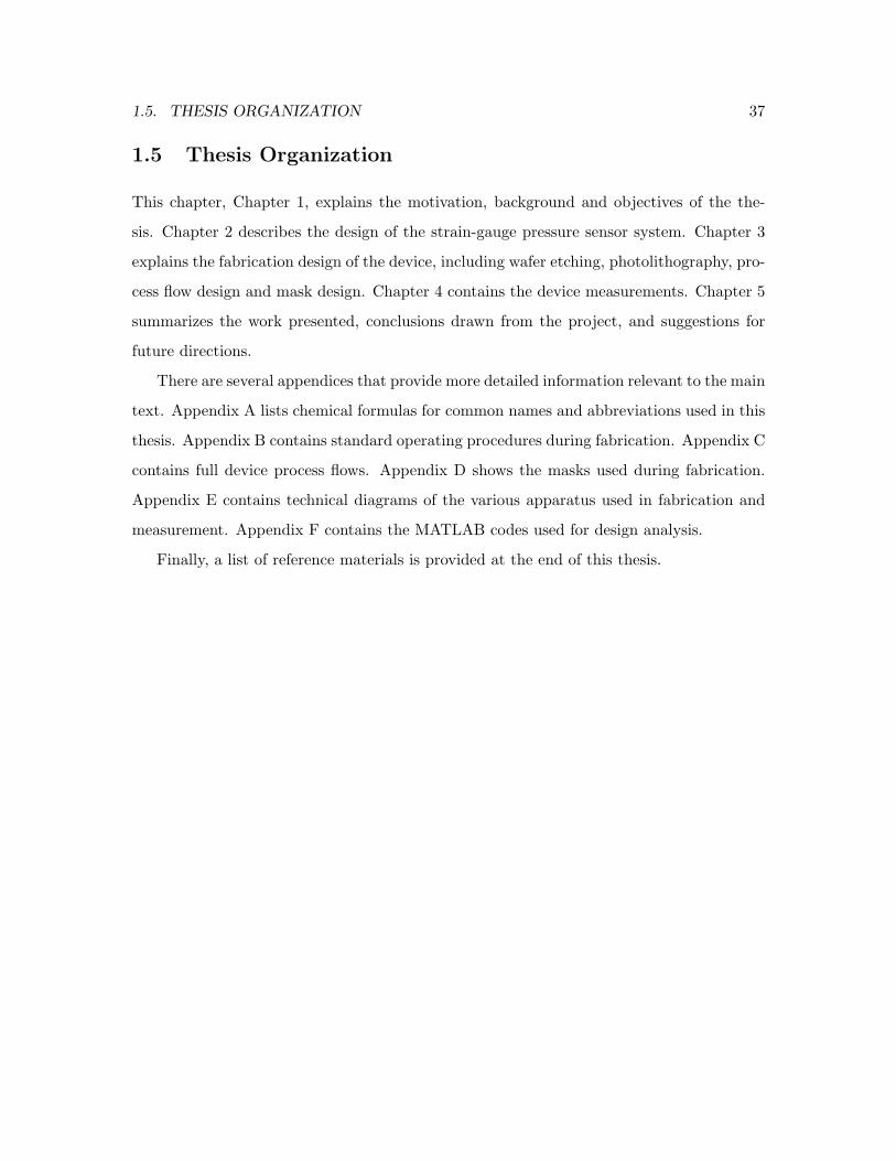
The strain-gauge pressure sensor system presented in this thesis consists of a set of MEMS
pressure sensors with side lengths on the order of 2 mm (2000 µm) spaced a few millime-
ters apart and fabricated on bonded silicon and Pyrex wafers. The pressure-sensing array
was fabricated in silicon and Pyrex for two primary reasons: the structural and electronic
properties of these materials, as well as their microfabrication technologies, are stable and
well understood. Additionally, silicon offers a controlled environment in which to develop
a pressure-sensing array. A future design of the pressure sensor system will take place in
polymer materials. The use of a strain gauge instead of silicon-specific technologies, such
as piezoresistors, is a design decision that renders the sensor transferrable to polymer-based
technologies. These sensors can be arranged over a surface in various piecewise linear con-
figurations, such as a single line, a patch consisting of several parallel lines or specialized
forms to approximate the shape of a vehicle’s hull or fins. Figure 2-1 shows one possible
configuration for the pressure system.
Length: ~140 mm
Thickness: ~1 mm
Diaphragm Size: ~2 mm
Spacing: ~2 mm
Silicon Device Layer: 20 µm
Buried Silicon Oxide Layer: 0.5 µm
Silicon Handle: ~0.5 mm
Pyrex Wafer: ~0.5 mm
Figure 2-1: Diagram of pressure-sensor array with basic structure depicted.
Each individual pressure sensor has a strain gauge, which is a set of four long and
2.1. OVERVIEW OF DEVICE FEATURES 41
narrow1 snaking resistors, mounted on a flexible thin (20 µm) square silicon diaphragm
attached at the edges to a square silicon cavity 2000 µm wide on each side. To create
a spatially-invariant reference pressure across the array, the cavities are interconnected to
one another through channels in both the silicon and Pyrex wafers. As the difference in
pressure above and below a particular diaphragm changes, the diaphragm bends2 and the
strain-gauge resistances change. To maximize the pressure sensitivity, the four resistors,
each on the order of 10 kΩ, are connected in a Wheatstone bridge configuration, which is
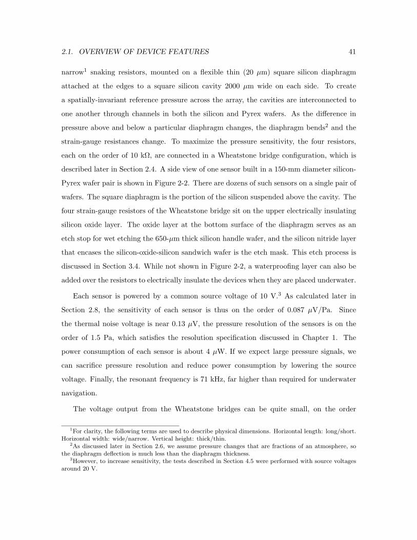
described later in Section 2.4. A side view of one sensor built in a 150-mm diameter silicon-
Pyrex wafer pair is shown in Figure 2-2. There are dozens of such sensors on a single pair of
wafers. The square diaphragm is the portion of the silicon suspended above the cavity. The
four strain-gauge resistors of the Wheatstone bridge sit on the upper electrically insulating
silicon oxide layer. The oxide layer at the bottom surface of the diaphragm serves as an
etch stop for wet etching the 650-µm thick silicon handle wafer, and the silicon nitride layer
that encases the silicon-oxide-silicon sandwich wafer is the etch mask. This etch process is
discussed in Section 3.4. While not shown in Figure 2-2, a waterproofing layer can also be
added over the resistors to electrically insulate the devices when they are placed underwater.
Each sensor is powered by a common source voltage of 10 V.3 As calculated later in
Section 2.8, the sensitivity of each sensor is thus on the order of 0.087 µV/Pa. Since
the thermal noise voltage is near 0.13 µV, the pressure resolution of the sensors is on the
order of 1.5 Pa, which satisfies the resolution specification discussed in Chapter 1. The
power consumption of each sensor is about 4 µW. If we expect large pressure signals, we
can sacrifice pressure resolution and reduce power consumption by lowering the source
voltage. Finally, the resonant frequency is 71 kHz, far higher than required for underwater
navigation.
The voltage output from the Wheatstone bridges can be quite small, on the order
1For clarity, the following terms are used to describe physical dimensions. Horizontal length: long/short.Horizontal width: wide/narrow. Vertical height: thick/thin.
2As discussed later in Section 2.6, we assume pressure changes that are fractions of an atmosphere, sothe diaphragm deflection is much less than the diaphragm thickness.
3However, to increase sensitivity, the tests described in Section 4.5 were performed with source voltagesaround 20 V.
42 CHAPTER 2. DEVICE DESIGN
Pyrex
Silicon
Nitride
Oxide
Silicon
Oxide
Resistor
150 mm
2000 um
500 um
650 um
20 um
Top view
Air cavity
Figure 2-2: Side view of a single sensor (not to scale). The diaphragm, outlined by the redsquare, is the portion of the silicon layer above the cavity. (Inset) Four long and narrowresistors (black) sit on the upper oxide layer (orange).
of microvolts. Therefore, in order to improve the signal-to-noise ratio of the sensor, we
amplify the signal with a simple measurement chain: a pair of sensing wires attached to
the bridge output of each sensor. Each pair of wires is fed into a set of off-wafer amplifying
circuits for data analysis. Another scheme for amplification is a set of integrated single-stage
differential amplifiers transistor circuits built into the wafer, one for each pressure sensor.
This integrated circuit is discussed in Section 5.3.

2.2. WAFER-LEVEL DESIGN 43
2.2 Wafer-Level Design
The wafer-level features of the pressure sensor systems designed and fabricated for this thesis
are described here. In all, five rounds of devices were developed to test various combinations
of components of the sensor system described in Section 2.1.
1. Pressure-activated diaphragms without strain-gauge resistors;
2. Electrically isolated strain-gauge resistors on dummy wafers;
3. Electrically isolated strain-gauge resistors on pressure-activated diaphragms;
4. Fully interconnected strain-gauge sensors on pressure-activated diaphragms without
amplifying transistors;
5. Fully interconnected strain-gauge sensors on pressure-activated diaphragms with am-
plifying transistors.
Rounds 1, 2, 3 and 4 have been fabricated and tested. Round 1 demonstrated the suitability
of thin silicon diaphragms for sensing pressure. Round 2 showed that our resistor design
can be reliably and repeatedly fabricated. Round 3 showed that the strain-gauge resistors
can act as pressure sensors. Round 4 enabled the devices to be used underwater. Round
5, left as future work, will reduce the noise and enable x-y addressing to allow for more
efficient use of input and output wires by integrating amplifier and array read-out circuitry
directly on the wafer.
2.2.1 Air channels
As discussed in Chapter 1, one of the challenges in designing the pressure sensor array is the
equilibration of back pressure, which is pressure applied to the back-side of the diaphragms
from within the sensor cavity. Since we are interested in detecting the small-signal pressure
across the entire array, we increase our signal-to-noise by removing the large-signal pressure
(DC component) via a common back pressure. We designed fluidic channels that enable the
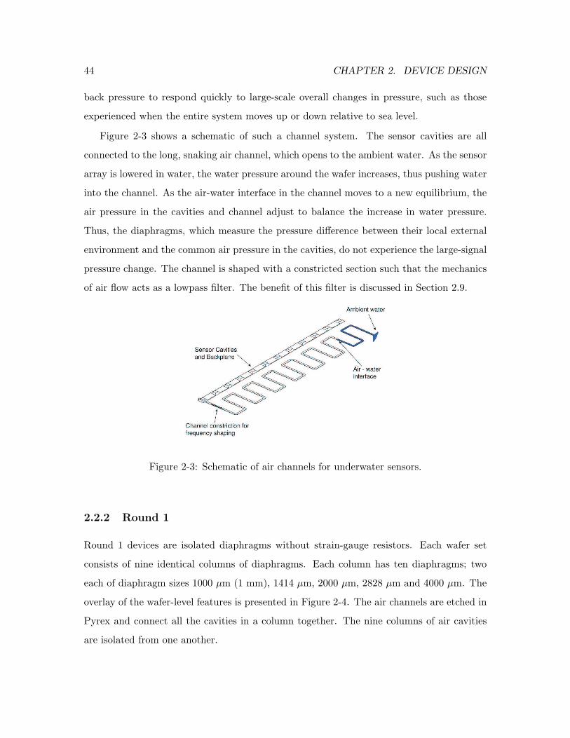
44 CHAPTER 2. DEVICE DESIGN
back pressure to respond quickly to large-scale overall changes in pressure, such as those
experienced when the entire system moves up or down relative to sea level.
Figure 2-3 shows a schematic of such a channel system. The sensor cavities are all
connected to the long, snaking air channel, which opens to the ambient water. As the sensor
array is lowered in water, the water pressure around the wafer increases, thus pushing water
into the channel. As the air-water interface in the channel moves to a new equilibrium, the
air pressure in the cavities and channel adjust to balance the increase in water pressure.
Thus, the diaphragms, which measure the pressure difference between their local external
environment and the common air pressure in the cavities, do not experience the large-signal
pressure change. The channel is shaped with a constricted section such that the mechanics
of air flow acts as a lowpass filter. The benefit of this filter is discussed in Section 2.9.
Figure 2-3: Schematic of air channels for underwater sensors.
2.2.2 Round 1
Round 1 devices are isolated diaphragms without strain-gauge resistors. Each wafer set
consists of nine identical columns of diaphragms. Each column has ten diaphragms; two
each of diaphragm sizes 1000 µm (1 mm), 1414 µm, 2000 µm, 2828 µm and 4000 µm. The
overlay of the wafer-level features is presented in Figure 2-4. The air channels are etched in
Pyrex and connect all the cavities in a column together. The nine columns of air cavities
are isolated from one another.
2.2. WAFER-LEVEL DESIGN 45
The wafer is diced into isolated columns, and one diaphragm in each column is deliber-
ately pierced. We interface the air channel to a syringe-controlled manometer4 via copper
tubes glued to the broken cavity. The manometer manipulates and measures the back
pressure, deflecting the diaphragm. Round 1 devices confirm that the deflection behavior
of the diaphragm is sufficiently consistent and sensitive to act as the mechanical sensing
component of the strain-gauge sensor.
2.2.3 Round 2
Round 2 simply consists of isolated strain-gauge resistors on dummy wafers. Each resistor
has large probe pads on each end. The cell-by-cell layout corresponds to that of Round 1
and the resistor layout is presented in Figure 2-5. The inset shows a single cell of resistors
and access pads for a 4 mm device. The design of the strain-gauge resistors is discussed in
Section 2.7. The resistors are visually examined under a microscope and their resistances
are measured.
4The operation of the manometer is described in Section 4.2.
46 CHAPTER 2. DEVICE DESIGN
Figure 2-4: Overlay of Round 1 devices (actual size). The wafer is 150 mm in diameter. Theair channels (blue) are etched in Pyrex and connect all the cavities in a column together.The bases of the cavities (red) are slightly wider than the diaphragms (black).
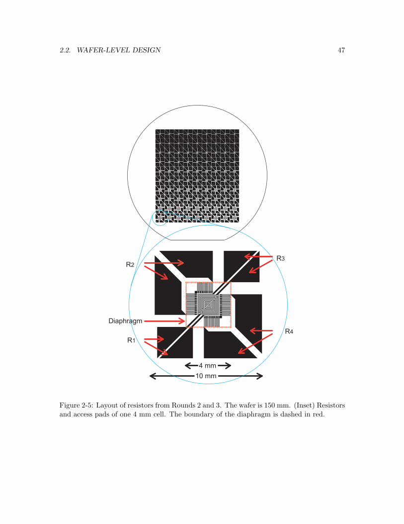
2.2. WAFER-LEVEL DESIGN 47
4 mm
10 mm
Diaphragm
R1
R2
R4
R3
Figure 2-5: Layout of resistors from Rounds 2 and 3. The wafer is 150 mm. (Inset) Resistorsand access pads of one 4 mm cell. The boundary of the diaphragm is dashed in red.

48 CHAPTER 2. DEVICE DESIGN
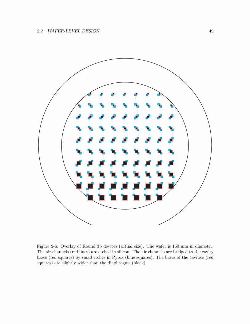
2.2.4 Round 3
Round 3 combines the first two rounds to build isolated strain-gauge resistors on pressure-
activated diaphragms. Two classes of Round 3 devices are fabricated.5 Round 3a devices
combines the resistor design of Round 2 (Figure 2-5) with the diaphragms and large air
channels etched in Pyrex of Round 1 (Figure 2-4). Round 3b modifies the air channels
to thin and narrow channels etched in silicon. The overlay of the wafer-level features is
presented in Figure 2-6. The thin and narrow channels alternate sides of the column to
reduce the risk of the silicon wafer from breaking. To further mitigate the risk, the silicon
channels do not run to the silicon cavities. Instead, the small gap is bridged by slight square
etches in Pyrex. Another improvement with Round 3b is the removal of the four sensors
at the corners of the wafer. The reason for this minor change is explained at the end of
Subsection 3.4.3.
The deflections of the diaphragms are manipulated as described in earlier for Round 1
by a manometer through a deliberately pierced cavity. Additionally, microscope probes are
attached to the resistor probe pads to electrically access the sensor as pressure is applied
from the back-side. Results from these experiments are discussed in Sections 4.3, 4.4 and
4.5.
5In addition to the design of the air channels, the fabrication processes for the two classes differed aswell. This is discussed in Section 3.2.
2.2. WAFER-LEVEL DESIGN 49
Figure 2-6: Overlay of Round 3b devices (actual size). The wafer is 150 mm in diameter.The air channels (red lines) are etched in silicon. The air channels are bridged to the cavitybases (red squares) by small etches in Pyrex (blue squares). The bases of the cavities (redsquares) are slightly wider than the diaphragms (black).
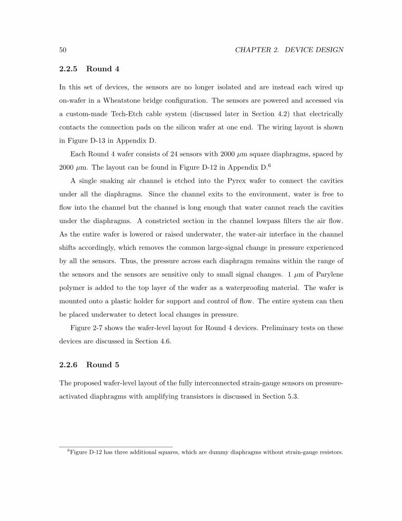
50 CHAPTER 2. DEVICE DESIGN
2.2.5 Round 4
In this set of devices, the sensors are no longer isolated and are instead each wired up
on-wafer in a Wheatstone bridge configuration. The sensors are powered and accessed via
a custom-made Tech-Etch cable system (discussed later in Section 4.2) that electrically
contacts the connection pads on the silicon wafer at one end. The wiring layout is shown
in Figure D-13 in Appendix D.
Each Round 4 wafer consists of 24 sensors with 2000 µm square diaphragms, spaced by
2000 µm. The layout can be found in Figure D-12 in Appendix D.6
A single snaking air channel is etched into the Pyrex wafer to connect the cavities
under all the diaphragms. Since the channel exits to the environment, water is free to
flow into the channel but the channel is long enough that water cannot reach the cavities
under the diaphragms. A constricted section in the channel lowpass filters the air flow.
As the entire wafer is lowered or raised underwater, the water-air interface in the channel
shifts accordingly, which removes the common large-signal change in pressure experienced
by all the sensors. Thus, the pressure across each diaphragm remains within the range of
the sensors and the sensors are sensitive only to small signal changes. 1 µm of Parylene
polymer is added to the top layer of the wafer as a waterproofing material. The wafer is
mounted onto a plastic holder for support and control of flow. The entire system can then
be placed underwater to detect local changes in pressure.
Figure 2-7 shows the wafer-level layout for Round 4 devices. Preliminary tests on these
devices are discussed in Section 4.6.
2.2.6 Round 5
The proposed wafer-level layout of the fully interconnected strain-gauge sensors on pressure-
activated diaphragms with amplifying transistors is discussed in Section 5.3.
6Figure D-12 has three additional squares, which are dummy diaphragms without strain-gauge resistors.
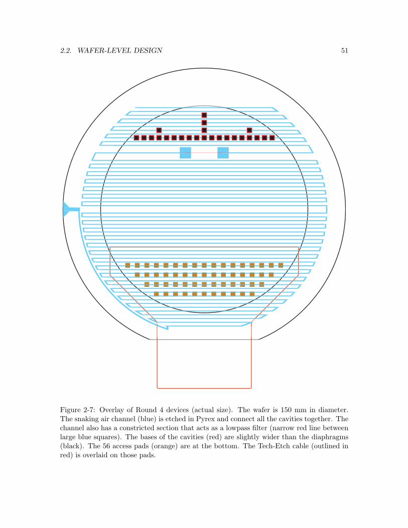
2.2. WAFER-LEVEL DESIGN 51
Figure 2-7: Overlay of Round 4 devices (actual size). The wafer is 150 mm in diameter.The snaking air channel (blue) is etched in Pyrex and connect all the cavities together. Thechannel also has a constricted section that acts as a lowpass filter (narrow red line betweenlarge blue squares). The bases of the cavities (red) are slightly wider than the diaphragms(black). The 56 access pads (orange) are at the bottom. The Tech-Etch cable (outlined inred) is overlaid on those pads.
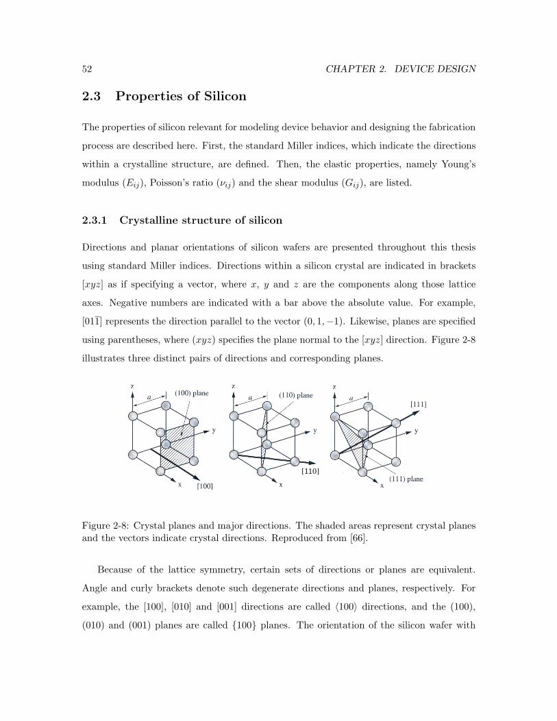
52 CHAPTER 2. DEVICE DESIGN
2.3 Properties of Silicon
The properties of silicon relevant for modeling device behavior and designing the fabrication
process are described here. First, the standard Miller indices, which indicate the directions
within a crystalline structure, are defined. Then, the elastic properties, namely Young’s
modulus (Eij), Poisson’s ratio (νij) and the shear modulus (Gij), are listed.
2.3.1 Crystalline structure of silicon
Directions and planar orientations of silicon wafers are presented throughout this thesis
using standard Miller indices. Directions within a silicon crystal are indicated in brackets
[xyz] as if specifying a vector, where x, y and z are the components along those lattice
axes. Negative numbers are indicated with a bar above the absolute value. For example,
[011] represents the direction parallel to the vector (0, 1,−1). Likewise, planes are specified
using parentheses, where (xyz) specifies the plane normal to the [xyz] direction. Figure 2-8
illustrates three distinct pairs of directions and corresponding planes.
[110]
Figure 2-8: Crystal planes and major directions. The shaded areas represent crystal planesand the vectors indicate crystal directions. Reproduced from [66].
Because of the lattice symmetry, certain sets of directions or planes are equivalent.
Angle and curly brackets denote such degenerate directions and planes, respectively. For
example, the [100], [010] and [001] directions are called 〈100〉 directions, and the (100),
(010) and (001) planes are called 100 planes. The orientation of the silicon wafer with
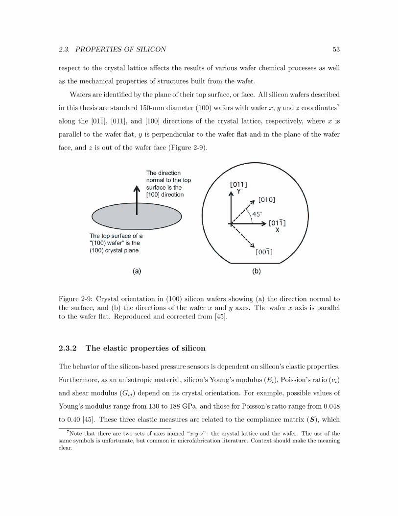
2.3. PROPERTIES OF SILICON 53
respect to the crystal lattice affects the results of various wafer chemical processes as well
as the mechanical properties of structures built from the wafer.
Wafers are identified by the plane of their top surface, or face. All silicon wafers described
in this thesis are standard 150-mm diameter (100) wafers with wafer x, y and z coordinates7
along the [011], [011], and [100] directions of the crystal lattice, respectively, where x is
parallel to the wafer flat, y is perpendicular to the wafer flat and in the plane of the wafer
face, and z is out of the wafer face (Figure 2-9).
Figure 2-9: Crystal orientation in (100) silicon wafers showing (a) the direction normal tothe surface, and (b) the directions of the wafer x and y axes. The wafer x axis is parallelto the wafer flat. Reproduced and corrected from [45].
2.3.2 The elastic properties of silicon
The behavior of the silicon-based pressure sensors is dependent on silicon’s elastic properties.
Furthermore, as an anisotropic material, silicon’s Young’s modulus (Ei), Poission’s ratio (νi)
and shear modulus (Gij) depend on its crystal orientation. For example, possible values of
Young’s modulus range from 130 to 188 GPa, and those for Poisson’s ratio range from 0.048
to 0.40 [45]. These three elastic measures are related to the compliance matrix (S), which
7Note that there are two sets of axes named “x-y-z”: the crystal lattice and the wafer. The use of thesame symbols is unfortunate, but common in microfabrication literature. Context should make the meaningclear.
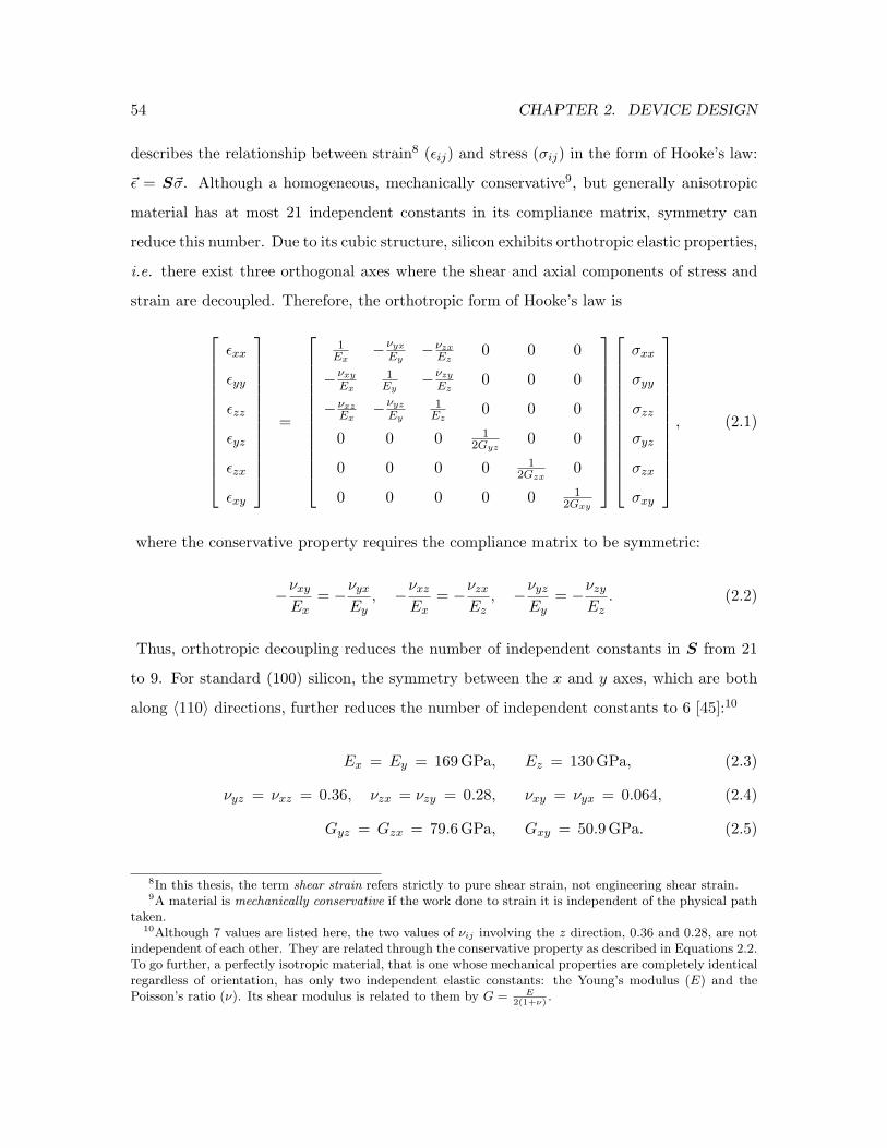
54 CHAPTER 2. DEVICE DESIGN
describes the relationship between strain8 (ǫij) and stress (σij) in the form of Hooke’s law:
~ǫ = S~σ. Although a homogeneous, mechanically conservative9, but generally anisotropic
material has at most 21 independent constants in its compliance matrix, symmetry can
reduce this number. Due to its cubic structure, silicon exhibits orthotropic elastic properties,
i.e. there exist three orthogonal axes where the shear and axial components of stress and
strain are decoupled. Therefore, the orthotropic form of Hooke’s law is
ǫxx
ǫyy
ǫzz
ǫyz
ǫzx
ǫxy
=
1Ex
−νyxEy
−νzxEz
0 0 0
−νxyEx
1Ey
−νzyEz
0 0 0
−νxzEx
−νyzEy
1Ez
0 0 0
0 0 0 12Gyz
0 0
0 0 0 0 12Gzx
0
0 0 0 0 0 12Gxy
σxx
σyy
σzz
σyz
σzx
σxy
, (2.1)
where the conservative property requires the compliance matrix to be symmetric:
−νxyEx
= −νyxEy
, −νxzEx
= −νzxEz
, −νyzEy
= −νzyEz
. (2.2)
Thus, orthotropic decoupling reduces the number of independent constants in S from 21
to 9. For standard (100) silicon, the symmetry between the x and y axes, which are both
along 〈110〉 directions, further reduces the number of independent constants to 6 [45]:10
Ex = Ey = 169GPa, Ez = 130GPa, (2.3)
νyz = νxz = 0.36, νzx = νzy = 0.28, νxy = νyx = 0.064, (2.4)
Gyz = Gzx = 79.6GPa, Gxy = 50.9GPa. (2.5)
8In this thesis, the term shear strain refers strictly to pure shear strain, not engineering shear strain.9A material is mechanically conservative if the work done to strain it is independent of the physical path
taken.10Although 7 values are listed here, the two values of νij involving the z direction, 0.36 and 0.28, are not
independent of each other. They are related through the conservative property as described in Equations 2.2.To go further, a perfectly isotropic material, that is one whose mechanical properties are completely identicalregardless of orientation, has only two independent elastic constants: the Young’s modulus (E) and thePoisson’s ratio (ν). Its shear modulus is related to them by G = E
2(1+ν).
2.3. PROPERTIES OF SILICON 55
Dopants typically alter silicon’s elastic properties by only up to 3%, so these effects can
be safely ignored for most calculations [45]. However, dopants can cause internal stress,
even if the bulk elastic properties do not change.
2.3.3 The elastic properties of thin silicon diaphragms
Since this thesis uses the elastic properties of silicon only in the context of thin silicon
diaphragms of length L in the wafer x and y directions (or the planar directions) and
uniform thickness H in the z direction, the relationship between stress and strain on the
top surface of the diaphragm given by Equation 2.1 can be further simplified as follows.
As discussed later in Section 2.6, for small diaphragm deflections, the vertical shear strains
ǫyz and ǫzx, and the normal strain ǫzz (and the corresponding stresses σyz, σzx and σzz)
are negligible compared to the planar axial strains ǫxx, ǫyy and ǫxy (and the corresponding
stresses σxx, σyy and σxy).11 With these assumptions, the planar axial components of strain
in terms of the planar axial components of stress are
ǫx =1
E(σx − νσy), (2.6)
ǫy =1
E(σy − νσx), (2.7)
and the planar axial stresses in terms of the planar axial strains are
σx =E
1− ν2(ǫx + νǫy), (2.8)
σy =E
1− ν2(ǫy + νǫx), (2.9)
where some subscripts are dropped for notational simplicity:
ǫx ≡ ǫxx, ǫy ≡ ǫyy, σx ≡ σxx, σy ≡ σyy, (2.10)
E ≡ Ex = Ey = 169GPa, ν ≡ νxy = νyx = 0.064. (2.11)
11Note that it is impossible for both ǫzz and σzz to be exactly zero simultaneously or else Equation 2.1would be over-constrained. For the purposes of this thesis, we will certainly assume σzz = 0, which iscommon in the literature [73, 84, 19].
56 CHAPTER 2. DEVICE DESIGN
These conventions are adopted in subsequent sections regarding (100) silicon.
The final set of material parameters for characterizing the behavior of the pressure sensor
is the flexural rigidities Dx, Dy and D0 of a two-dimensional diaphragm with thickness H
made of (100) silicon:
Dx =ExH
3
12(1− νxyνyx)= (14.1GPa)×H3, (2.12)
Dy =EyH
3
12(1− νxyνyx)= (14.1GPa)×H3, (2.13)
D0 =ExνxyH
3
12(1− νxyνyx)= (0.905GPa)×H3. (2.14)
Likewise, the torsional rigidity is
Dxy =GxyH
3
12= (4.24GPa)×H3. (2.15)
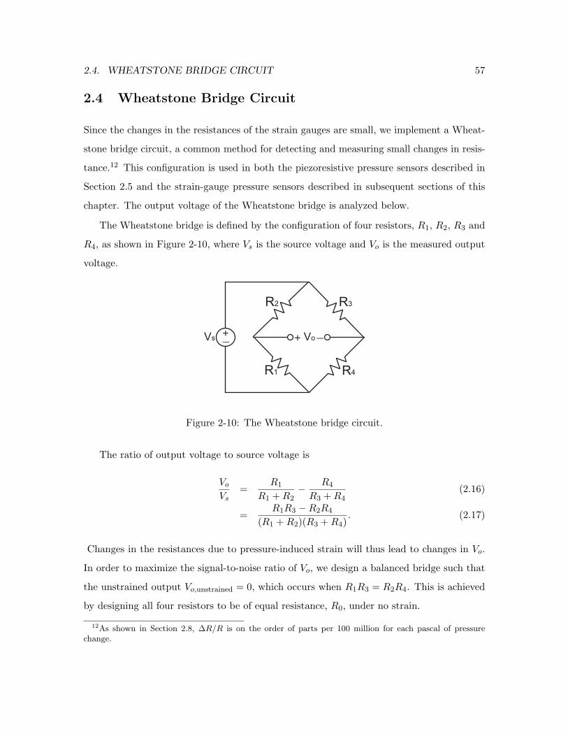
2.4. WHEATSTONE BRIDGE CIRCUIT 57
2.4 Wheatstone Bridge Circuit
Since the changes in the resistances of the strain gauges are small, we implement a Wheat-
stone bridge circuit, a common method for detecting and measuring small changes in resis-
tance.12 This configuration is used in both the piezoresistive pressure sensors described in
Section 2.5 and the strain-gauge pressure sensors described in subsequent sections of this
chapter. The output voltage of the Wheatstone bridge is analyzed below.
The Wheatstone bridge is defined by the configuration of four resistors, R1, R2, R3 and
R4, as shown in Figure 2-10, where Vs is the source voltage and Vo is the measured output
voltage.
R1
+ +_ _Vs Vo
R4
R3R2
Figure 2-10: The Wheatstone bridge circuit.
The ratio of output voltage to source voltage is
Vo
Vs=
R1
R1 +R2−
R4
R3 +R4(2.16)
=R1R3 −R2R4
(R1 +R2)(R3 +R4). (2.17)
Changes in the resistances due to pressure-induced strain will thus lead to changes in Vo.
In order to maximize the signal-to-noise ratio of Vo, we design a balanced bridge such that
the unstrained output Vo,unstrained = 0, which occurs when R1R3 = R2R4. This is achieved
by designing all four resistors to be of equal resistance, R0, under no strain.
12As shown in Section 2.8, ∆R/R is on the order of parts per 100 million for each pascal of pressurechange.

58 CHAPTER 2. DEVICE DESIGN
Let αi be the relative change in resistance, or ∆Ri/Ri, upon strain. The resistances
change to new values
Ri,new = (1 + αi)Ri,old ∀i ∈ [1, 4] (2.18)
= (1 + αi)R0. (2.19)
Substituting the new strained Ri values into Equation 2.17, we see that |Vo/Vs| is maximized
when α1 and α3 have the same sign, and α2 and α4 also have the same sign, but opposite
that of α1 and α3. We further choose diagonally opposite resistors to be identical so that
α1 = α3 and α2 = α4. Then, the ratio of Vo to Vs is
Vo
Vs=
(1 + α1)2R2
0 − (1 + α2)2R2
0
(2 + α1 + α2)2R20
(2.20)
=(1 + α1 + 1 + α2)(1 + α1 − 1− α2)
(2 + α1 + α2)2(2.21)
=(2 + α1 + α2)(α1 − α2)
(2 + α1 + α2)2(2.22)
Vo
Vs=
α1 − α2
2 + α1 + α2≈
α1 − α2
2, (2.23)
where the final approximation assumes αi ≪ 1. Equation 2.23 is used later in Sections 2.5
and 2.8 to calculate the sensitivities of standard piezoresistive pressure sensors as well as
our strain-gauge pressure sensors.
It can similarly be shown that when only R1 and R2 undergo relative changes α1 and
α2, respectively, and R3 and R4 remain fixed at R0, thus forming a half bridge, the ratio of
Vo to Vs is
Vo
Vs
∣
∣
∣
∣
half
=α1 − α2
2(2 + α1 + α2)≈
α1 − α2
4, (2.24)
or half the sensitivity of the full bridge. Finally, when only a single resistor R1 undergoes
a relative change α1 and all the other resistors remain fixed at R0, thus forming a quarter

2.4. WHEATSTONE BRIDGE CIRCUIT 59
bridge, the ratio of Vo to Vs is
Vo
Vs
∣
∣
∣
∣
quarter
=α1
2(2 + α1)≈
α1
4. (2.25)
Equation 2.25 is used later in Sections 4.4 and 4.5 when fabricated strain-gauge resistors
are individually tested.
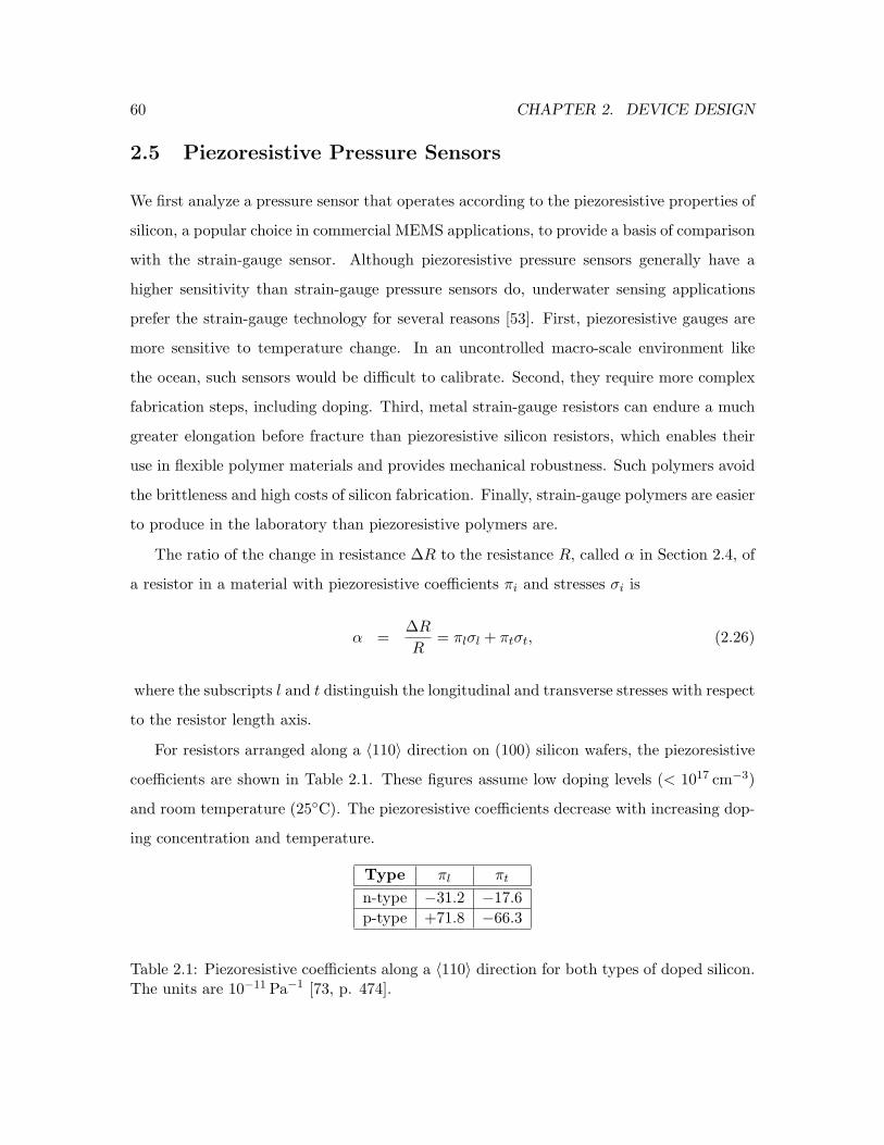
60 CHAPTER 2. DEVICE DESIGN
2.5 Piezoresistive Pressure Sensors
We first analyze a pressure sensor that operates according to the piezoresistive properties of
silicon, a popular choice in commercial MEMS applications, to provide a basis of comparison
with the strain-gauge sensor. Although piezoresistive pressure sensors generally have a
higher sensitivity than strain-gauge pressure sensors do, underwater sensing applications
prefer the strain-gauge technology for several reasons [53]. First, piezoresistive gauges are
more sensitive to temperature change. In an uncontrolled macro-scale environment like
the ocean, such sensors would be difficult to calibrate. Second, they require more complex
fabrication steps, including doping. Third, metal strain-gauge resistors can endure a much
greater elongation before fracture than piezoresistive silicon resistors, which enables their
use in flexible polymer materials and provides mechanical robustness. Such polymers avoid
the brittleness and high costs of silicon fabrication. Finally, strain-gauge polymers are easier
to produce in the laboratory than piezoresistive polymers are.
The ratio of the change in resistance ∆R to the resistance R, called α in Section 2.4, of
a resistor in a material with piezoresistive coefficients πi and stresses σi is
α =∆R
R= πlσl + πtσt, (2.26)
where the subscripts l and t distinguish the longitudinal and transverse stresses with respect
to the resistor length axis.
For resistors arranged along a 〈110〉 direction on (100) silicon wafers, the piezoresistive
coefficients are shown in Table 2.1. These figures assume low doping levels (< 1017 cm−3)
and room temperature (25C). The piezoresistive coefficients decrease with increasing dop-
ing concentration and temperature.
Type πl πt
n-type −31.2 −17.6
p-type +71.8 −66.3
Table 2.1: Piezoresistive coefficients along a 〈110〉 direction for both types of doped silicon.The units are 10−11 Pa−1 [73, p. 474].
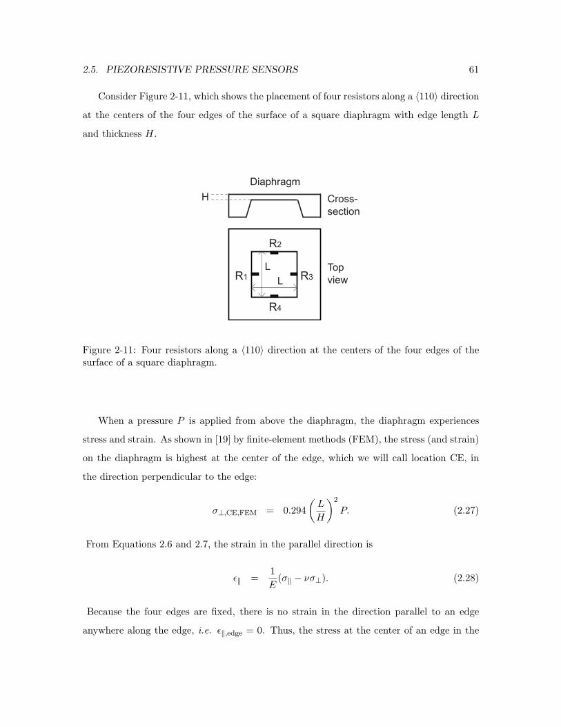
2.5. PIEZORESISTIVE PRESSURE SENSORS 61
Consider Figure 2-11, which shows the placement of four resistors along a 〈110〉 direction
at the centers of the four edges of the surface of a square diaphragm with edge length L
and thickness H.
R1
R2
R3
R4
Cross-
section
Diaphragm
Top
viewL
L
H
Figure 2-11: Four resistors along a 〈110〉 direction at the centers of the four edges of thesurface of a square diaphragm.
When a pressure P is applied from above the diaphragm, the diaphragm experiences
stress and strain. As shown in [19] by finite-element methods (FEM), the stress (and strain)
on the diaphragm is highest at the center of the edge, which we will call location CE, in
the direction perpendicular to the edge:
σ⊥,CE,FEM = 0.294
(
L
H
)2
P. (2.27)
From Equations 2.6 and 2.7, the strain in the parallel direction is
ǫ‖ =1
E(σ‖ − νσ⊥). (2.28)
Because the four edges are fixed, there is no strain in the direction parallel to an edge
anywhere along the edge, i.e. ǫ‖,edge = 0. Thus, the stress at the center of an edge in the

62 CHAPTER 2. DEVICE DESIGN
direction parallel to the edge is
σ‖,CE,FEM = νσ⊥,CE,FEM (2.29)
= 0.064× 0.294
(
L
H
)2
P (2.30)
= 0.019
(
L
H
)2
P. (2.31)
For typical dimensions L = 2000µm and H = 20µm, this produces
σ⊥,CE,FEM = 2940P, (2.32)
σ‖,CE,FEM = 190P. (2.33)
Since σ⊥,CE,FEM is more than 15 times σ‖,CE,FEM, one of the terms in Equation 2.26
dominates the other, which helps us choose the optimal type of silicon in which to build
piezoresistors. The absolute values of πl and πt for p-type silicon are larger than those for
n-type silicon, which implies more sensitivity to stress. Additionally, the coefficients for the
two orthogonal directions in p-type silicon have opposing signs, which is appropriate for the
Wheatstone bridge described earlier. Thus, we choose p-type silicon as the substrate for
the piezoresistive pressure sensor.
We use Equations 2.32 and 2.33 and Table 2.1 to calculate the relative resistance change
α in Equation 2.26 for the four resistors. For R1 and R3, where the longitudinal direction
of the resistors is perpendicular to the diaphragm edge, the change is
α1 = πlσ⊥,CE,FEM + πtσ‖,CE,FEM (2.34)
= (71.8× 10⁻¹¹ Pa−1)(2940P ) + (−66.3× 10⁻¹¹ Pa−1)(190P ) (2.35)
= (1.98× 10⁻⁶ Pa−1)P . (2.36)
Similarly, the relative change in resistance for R2 and R4 is found by reversing the transverse
2.5. PIEZORESISTIVE PRESSURE SENSORS 63
and longitudinal stresses:
α2 = πlσ‖,CE,FEM + πtσ⊥,CE,FEM (2.37)
= (71.8× 10⁻¹¹ Pa−1)(190P ) + (−66.3× 10⁻¹¹ Pa−1)(2940P ) (2.38)
= (−1.81× 10⁻⁶ Pa−1)P . (2.39)
Applying these values to the relationship between the output voltage and source voltage
of a Wheatstone bridge, shown in Equation 2.23, with the assumption that P ≪ 106 Pa,
we obtain
Vo
Vs≈ (1.90× 10⁻⁶ Pa−1)P. (2.40)
For a typical source voltage of 10 V, this corresponds to a sensitivity of 19.0µV/Pa.
64 CHAPTER 2. DEVICE DESIGN
2.6 Mechanical Model of the Diaphragm
Now that piezoresistive pressure sensors have been studied, let us move on to strain-gauge
resistors. First, we develop a mechanical model of the diaphragms that form the basis of the
strain-gauge pressure sensors. This includes understanding the deflection of the diaphragm
and the strains on the diaphragm surface as pressure is applied. Later, in Section 2.7, we
show how this information aids in optimizing the design of the strain-gauge resistors.
2.6.1 Diaphragm assumptions
We begin by assuming the mechanical behavior of the diaphragm is dominated by the silicon
layer as it is far thicker than the other materials deposited or bonded to it. Next, to model
the behavior of the diaphragm, we use the linear, elastic, small-deflection theory of bending
for thin plates13, called Kirchhoff-Love plate theory, which assumes the following:
1. The material of the plate is elastic and homogeneous (though not necessarily isotropic14).
2. The plate is initially flat at zero applied pressure.
3. The normal deflection of the plate is small compared to the thickness of the plate,
which in turn is small compared to the length and width of the plate. Thus, the slope
of the deflected surface is very small.
4. The thickness of the plate does not change during deformation.
5. The middle surface of the plate, which is halfway between and parallel to the top and
bottom plate surfaces, remains unstrained and unstressed during deformation.
6. The vertical shear strains and the normal strain (and the corresponding stresses) are
negligible compared to the planar strains (and the corresponding stresses).
Furthermore, we assume that the plate is clamped on all four sides. However, in reality,
silicon cannot be ideally clamped [25].
13There is a subtle, but important, distinction between the terms “plate” and “diaphragm”. A plate is anideal mathematical construct, whereas a diaphragm is a realized physical structure. Thus, we are modelingthe silicon diphragm as a plate.
14The material used in this thesis, silicon, is orthotropic.
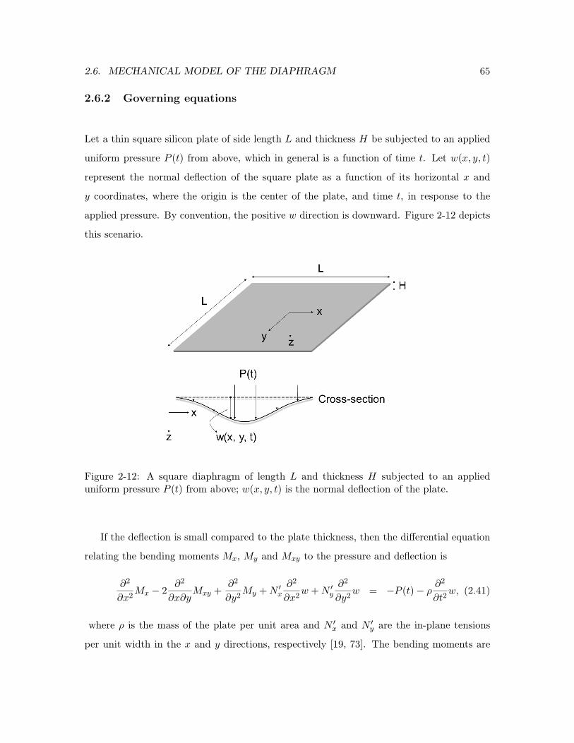
2.6. MECHANICAL MODEL OF THE DIAPHRAGM 65
2.6.2 Governing equations
Let a thin square silicon plate of side length L and thickness H be subjected to an applied
uniform pressure P (t) from above, which in general is a function of time t. Let w(x, y, t)
represent the normal deflection of the square plate as a function of its horizontal x and
y coordinates, where the origin is the center of the plate, and time t, in response to the
applied pressure. By convention, the positive w direction is downward. Figure 2-12 depicts
this scenario.
Figure 2-12: A square diaphragm of length L and thickness H subjected to an applieduniform pressure P (t) from above; w(x, y, t) is the normal deflection of the plate.
If the deflection is small compared to the plate thickness, then the differential equation
relating the bending moments Mx, My and Mxy to the pressure and deflection is
∂2
∂x2Mx − 2
∂2
∂x∂yMxy +
∂2
∂y2My +N ′
x
∂2
∂x2w +N ′
y
∂2
∂y2w = −P (t)− ρ
∂2
∂t2w, (2.41)
where ρ is the mass of the plate per unit area and N ′x and N ′
y are the in-plane tensions
per unit width in the x and y directions, respectively [19, 73]. The bending moments are
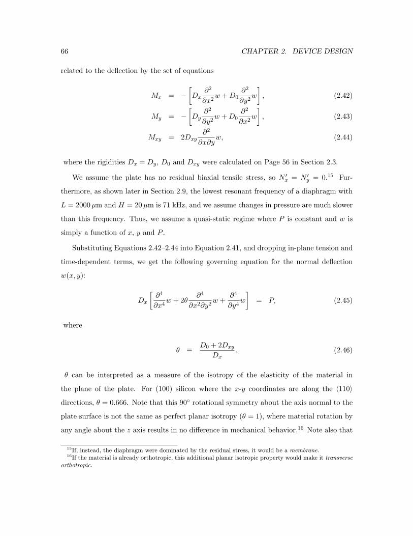
66 CHAPTER 2. DEVICE DESIGN
related to the deflection by the set of equations
Mx = −
[
Dx∂2
∂x2w +D0
∂2
∂y2w
]
, (2.42)
My = −
[
Dy∂2
∂y2w +D0
∂2
∂x2w
]
, (2.43)
Mxy = 2Dxy∂2
∂x∂yw, (2.44)
where the rigidities Dx = Dy, D0 and Dxy were calculated on Page 56 in Section 2.3.
We assume the plate has no residual biaxial tensile stress, so N ′x = N ′
y = 0.15 Fur-
thermore, as shown later in Section 2.9, the lowest resonant frequency of a diaphragm with
L = 2000µm and H = 20µm is 71 kHz, and we assume changes in pressure are much slower
than this frequency. Thus, we assume a quasi-static regime where P is constant and w is
simply a function of x, y and P .
Substituting Equations 2.42–2.44 into Equation 2.41, and dropping in-plane tension and
time-dependent terms, we get the following governing equation for the normal deflection
w(x, y):
Dx
[
∂4
∂x4w + 2θ
∂4
∂x2∂y2w +
∂4
∂y4w
]
= P, (2.45)
where
θ ≡D0 + 2Dxy
Dx. (2.46)
θ can be interpreted as a measure of the isotropy of the elasticity of the material in
the plane of the plate. For (100) silicon where the x-y coordinates are along the 〈110〉
directions, θ = 0.666. Note that this 90 rotational symmetry about the axis normal to the
plate surface is not the same as perfect planar isotropy (θ = 1), where material rotation by
any angle about the z axis results in no difference in mechanical behavior.16 Note also that
15If, instead, the diaphragm were dominated by the residual stress, it would be a membrane.16If the material is already orthotropic, this additional planar isotropic property would make it transverse
orthotropic.
2.6. MECHANICAL MODEL OF THE DIAPHRAGM 67
instead of using a shear modulus of Gxy = 50.9GPa [45], some previous work [6, 19, 7] use
Gxy = 62.2GPa, which corresponds to θ = 0.798.
The boundary conditions at the edges are
w
(
x = ±L
2or y = ±
L
2
)
= 0,∂
∂xw
(
x = ±L
2
)
=∂
∂yw
(
y = ±L
2
)
= 0. (2.47)
Although ideally clamped edges (expressed as the second boundary condition) are not
physically possible, this effect is only influential near the edges.
2.6.3 The nature of the deflection function
While the normal deflection w, and by extension, the stress and strain, for circular plates
are known in closed form, analytic solutions to Equation 2.45 with boundary conditions
Equation 2.47 do not exist for rectangular diaphragms. Various quasi-analytical and nu-
merical analyses have been performed [73, 84, 26, 3, 65, 6, 7, 19, 68]. Generally, w is in the
form of an infinite series of raised cosine terms [26, 84]. The first-order term sufficiently
models the diaphragm deflection for the purposes of this thesis. Following [73], w can be
approximated as a function of the form
w(x, y) =c14
[
1 + cos
(
2πx
L
)][
1 + cos
(
2πy
L
)]
, (2.48)
where the origin is the center of the plate and c1 is the deflection at the center of the plate,
which is where the deflection is greatest.17
While previous work has focused on reducing the square errors between the modeled and
experimental deflections, little work has been done on accurately modeling the stress and
strain on the surface of the diaphragm. Since these quantities depend on the second spatial
derivatives of the deflection function instead of the deflection itself, accurately modeling the
deflection function may not necessarily improve the spatial derivatives. Furthermore, any
discrepancies produced by these models would be masked by other simplifications to our
17The subscript in c1 refers to the fact that it is the amplitude of the first mode of vibration for thediaphragm. This thesis does not discuss other modes, but the notation is used for consistency with otherworks.
68 CHAPTER 2. DEVICE DESIGN
diaphragm model, including ignoring the effects of multiple materials on the diaphragm,
variations in the diaphragm thickness, residual stress and material imperfections in the
strain-gauge resistors, such as fractures and holes. These effects are discussed in Sections 4.3
and 4.5.
2.6.4 Deflection as a function of pressure
In general, the relationship between applied pressure P and the deflection at the center of
the plate c1 is given by the following three-term equation:
P =
Cr
[
σ0H
L2
]
+ Cb
[
EH3
(1− ν2)L4
]
c1 + Csfs(ν)
[
EH
(1− ν)L4
]
c31, (2.49)
where Cr, Cb and Cs are constants, σ0 is residual stress in the diaphragm, and fs(ν) is a
function of ν [73]. The first term, linear in c1, is due to residual stress, which we assume
is nonexistent in our devices. The second term, also linear, is due to bending. Finally, the
third term, a cubic, is due to stretching. When the maximum deflection is less than the plate
thickness, we can assume a model where there is no stretching. Thus, the pressure-deflection
model relationship is:
P = Cb
[
EH3
(1− ν2)L4
]
c1. (2.50)
Writing c1 in terms of P and defining the constant KE ≡ 1/Cb, we get:
c1 = KE
[
(1− ν2)L4
EH3
]
P. (2.51)
In the literature, the deflection-pressure relationship is often written in terms of the flexural
rigidity Dx = EH3
12(1−ν2):
c1 = KD
[
L4
Dx
]
P, (2.52)
2.6. MECHANICAL MODEL OF THE DIAPHRAGM 69
where the two constants are related by
KD =KE
12. (2.53)
The value ofKD for anisotropic (100) silicon with coordinates along the 〈110〉 directions has
been measured by several groups. [6] and [7] separately obtained the value KD = 0.00133
using different methods.18 [19] obtained KD = 0.001638 using finite-element analysis. In
light of the fact that the KD = 0.00133 value was published eight years after the KD =
0.001638 value, and by two separate groups employing different techniques, this thesis uses
KD = 0.00133. As noted earlier, all of these sources use a slightly different value for the
shear modulus Gxy than is generally accepted. Isotropic materials, on the other hand, have
a well-known KD = 0.00126 [84, 26, 3, 65]. For simplicity sake, some researchers use this
value even for anisotropic silicon.
For KD = 0.00133, ν = 0.064, E = 169 GPa, L = 2000µm, H = 20µm, the center
deflection to pressure ratio is
c1P
= 0.188 nm/Pa. (2.54)
Thus, one atmosphere (101.3 kPa) of pressure produces a center deflection of 19 µm.
Since the maximum pressure applied to the sensors is on the order of a few percent of an
atmosphere, the deflection is much less than the diaphragm thickness H, which satisfies
one of the conditions of Kirchhoff-Love plate theory. We will set a conservative limit for
deflection to be 10% of the diaphragm thickness. For a 2000 µm diaphragm, this corresponds
to a maximum applied pressure of 10.6 kPa.
Measurements of the deflection-pressure relationship for various fabricated diaphragms
are presented in Section 4.3.
18[6] models the deflection w with an infinite series of sinusoids and hyperbolic functions, whereas [7] usesan infinite polynomial.
70 CHAPTER 2. DEVICE DESIGN
2.6.5 Strain as a function of pressure
We seek to calculate the strain experienced by the diaphragm due to deflection by pressure.
The x- and y-components of strain on the top surface of the diaphragm are
ǫx(x, y) =H
2
∂2
∂x2w(x, y), (2.55)
ǫy(x, y) =H
2
∂2
∂y2w(x, y). (2.56)
Since shear strain merely translates the infinitesimal parallel resistors that make up a local
section of a resistor relative to one another without changing their lengths or widths, it
does not affect the resistance of strain-gauge resistors bound to the diaphragm surface.
Thus, shear strain is omitted. As first described on Page 67, we use the following to model
deflection w as a function of the center deflection c1:
w(x, y, c1) =c14
[
1 + cos
(
2πx
L
)][
1 + cos
(
2πy
L
)]
. (2.57)
The second derivative of w with respect to x is
∂2
∂x2w =
∂
∂x
(
∂
∂x
(
c14
[
1 + cos
(
2πx
L
)][
1 + cos
(
2πy
L
)]))
(2.58)
=c14
∂
∂x
[
−2π
Lsin
(
2πx
L
)][
1 + cos
(
2πy
L
)]
(2.59)
= −c14
(
2π
L
)2
cos
(
2πx
L
)[
1 + cos
(
2πy
L
)]
(2.60)
∂2
∂x2w = −c1
(π
L
)2cos
(
2πx
L
)[
1 + cos
(
2πy
L
)]
. (2.61)
Thus, the x-component of strain is
ǫx(x, y, c1) = −c1H
2
(π
L
)2cos
(
2πx
L
)[
1 + cos
(
2πy
L
)]
. (2.62)
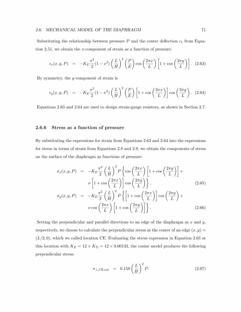
2.6. MECHANICAL MODEL OF THE DIAPHRAGM 71
Substituting the relationship between pressure P and the center deflection c1 from Equa-
tion 2.51, we obtain the x-component of strain as a function of pressure:
ǫx(x, y, P ) = −KEπ2
2(1− ν2)
(
L
H
)2(P
E
)
cos
(
2πx
L
)[
1 + cos
(
2πy
L
)]
. (2.63)
By symmetry, the y-component of strain is
ǫy(x, y, P ) = −KEπ2
2(1− ν2)
(
L
H
)2(P
E
)[
1 + cos
(
2πx
L
)]
cos
(
2πy
L
)
. (2.64)
Equations 2.63 and 2.64 are used to design strain-gauge resistors, as shown in Section 2.7.
2.6.6 Stress as a function of pressure
By substituting the expressions for strain from Equations 2.63 and 2.64 into the expressions
for stress in terms of strain from Equations 2.8 and 2.9, we obtain the components of stress
on the surface of the diaphragm as functions of pressure:
σx(x, y, P ) = −KEπ2
2
(
L
H
)2
P
cos
(
2πx
L
)[
1 + cos
(
2πy
L
)]
+
ν
[
1 + cos
(
2πx
L
)]
cos
(
2πy
L
)
, (2.65)
σy(x, y, P ) = −KEπ2
2
(
L
H
)2
P
[
1 + cos
(
2πx
L
)]
cos
(
2πy
L
)
+
ν cos
(
2πx
L
)[
1 + cos
(
2πy
L
)]
. (2.66)
Setting the perpendicular and parallel directions to an edge of the diaphragm as x and y,
respectively, we choose to calculate the perpendicular stress at the center of an edge (x, y) =
(L/2, 0), which we called location CE. Evaluating the stress expression in Equation 2.65 at
this location with KE = 12×KD = 12× 0.00133, the cosine model produces the following
perpendicular stress:
σ⊥,CE,cos = 0.158
(
L
H
)2
P. (2.67)
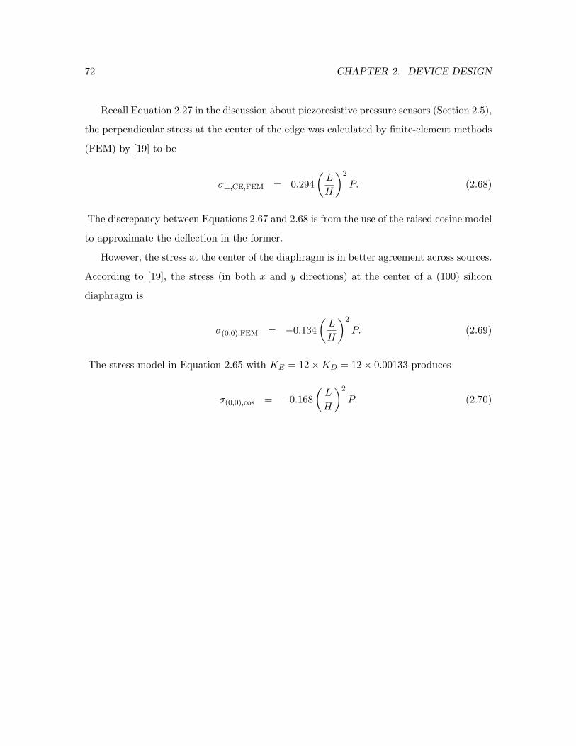
72 CHAPTER 2. DEVICE DESIGN
Recall Equation 2.27 in the discussion about piezoresistive pressure sensors (Section 2.5),
the perpendicular stress at the center of the edge was calculated by finite-element methods
(FEM) by [19] to be
σ⊥,CE,FEM = 0.294
(
L
H
)2
P. (2.68)
The discrepancy between Equations 2.67 and 2.68 is from the use of the raised cosine model
to approximate the deflection in the former.
However, the stress at the center of the diaphragm is in better agreement across sources.
According to [19], the stress (in both x and y directions) at the center of a (100) silicon
diaphragm is
σ(0,0),FEM = −0.134
(
L
H
)2
P. (2.69)
The stress model in Equation 2.65 with KE = 12×KD = 12× 0.00133 produces
σ(0,0),cos = −0.168
(
L
H
)2
P. (2.70)
2.7. STRAIN-GAUGE RESISTORS 73
2.7 Strain-Gauge Resistors
The design of the four strain-gauge resistors, the sensing element of the devices, is explained
below. Clearly, to maximize the sensitivity, the resistors should be concentrated at the high-
strain points. However, the conduction lines that connect the Wheatstone bridge to the
source voltage Vs have non-negligible resistances, as they have lengths on the centimeter
scale. In order to reduce the relative voltage drop on these conduction lines and maximize Vs
of the Wheatstone bridge, we increase the strain-gauge resistances, which entails occupying
other, less sensitive, areas of the diaphragm surface with parts of the strain gauges. The
gains in boosting the effective source voltage powering the bridge outweigh the losses in
overall relative change in strain-gauge resistances. To increase the resistances of the strain
gauges, we maximize the length of the resistors and minimize the cross-sectional area. Over
an L×L square diaphragm, a snaking line resistor of width L/n increases the total length by
∼n while reducing the cross-sectional area by another ∼n, resulting in an ∼n2 increase in
resistance. Thus it is ideal to have closely spaced, narrow snaking lines of resistance across
the entire diaphragm to maximize the resistance. This minimum width and spacing between
lines is limited by the resolution of photolithography, which is discussed in Section 3.3.
2.7.1 Relative change in resistance of an infinitesimally small resistor
Consider an infinitesimally small metal resistor dR bonded to the top surface of the silicon
diaphragm. Under deformation by the diaphragm, the x- and y-components of strain are
transferred to the resistor. We assume that the vertical height of the resistor is far thinner
than the diaphragm, so it does not contribute to the deformation mechanics as analyzed
earlier. For small strains, as assumed by Kirchhoff-Love plate theory, the relative change in
resistance as a result of diaphragm deformation is
αdR =∆dR
dR= ǫl − ǫw − ǫh, (2.71)
74 CHAPTER 2. DEVICE DESIGN
where l, w and h are the components of strain experienced by the resistor along its length,
width and height, respectively.19 The strains along the length and width of the resistor
are set by the two-dimensional strains of the diaphragm, depending on orientation, and the
strain along the height is related to the other two as
ǫh =−νR1− νR
(ǫl + ǫw), (2.72)
where νR is the isotropic Poisson’s ratio of the resistor material. Thus, the relative change
in resistance in terms of the surface strains is
αdR =∆dR
dR= ǫl − ǫw −
−νR1− νR
(ǫl + ǫw) (2.73)
=1
1− νRǫl +
2νR − 1
1− νRǫw. (2.74)
2.7.2 Simulating resistance change
For a real resistor of resistance R, the overall relative change is the weighted average relative
change of its infinitesimal components, integrating lengthwise:
α =1
R
∫
αdRdR (2.75)
=1
R
∫
s
αdR(s)ρ
A(s)ds, (2.76)
where s is the distance along the length of the resistor, ρ is the resistivity and A(s) is the
cross-sectional area as a function of s.
To simplify the resistor design, we constrain the resistor shape so that it consists of
piecewise linear components whose lengths and widths are along the x and y diaphragm
axes. Given these constraints, a MATLAB simulation, resistor design.m, was written
to aid resistor design according to the model described above. The expressions for the
19Increases in length increase the resistance, whereas decreases in the cross-sectional area (width andheight) increase the resistance.
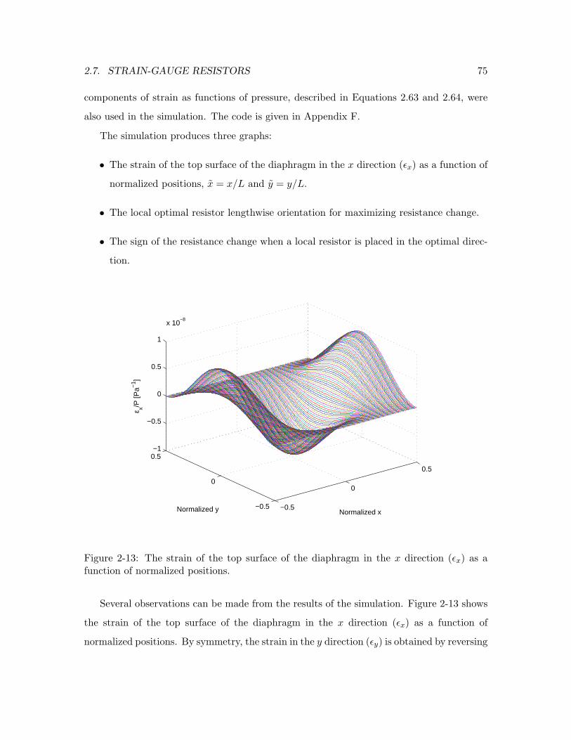
2.7. STRAIN-GAUGE RESISTORS 75
components of strain as functions of pressure, described in Equations 2.63 and 2.64, were
also used in the simulation. The code is given in Appendix F.
The simulation produces three graphs:
• The strain of the top surface of the diaphragm in the x direction (ǫx) as a function of
normalized positions, x = x/L and y = y/L.
• The local optimal resistor lengthwise orientation for maximizing resistance change.
• The sign of the resistance change when a local resistor is placed in the optimal direc-
tion.
−0.5
0
0.5
−0.5
0
0.5−1
−0.5
0
0.5
1
x 10−8
Normalized xNormalized y
ε x/P [P
a−1 ]
Figure 2-13: The strain of the top surface of the diaphragm in the x direction (ǫx) as afunction of normalized positions.
Several observations can be made from the results of the simulation. Figure 2-13 shows
the strain of the top surface of the diaphragm in the x direction (ǫx) as a function of
normalized positions. By symmetry, the strain in the y direction (ǫy) is obtained by reversing
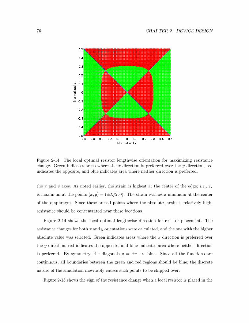
76 CHAPTER 2. DEVICE DESIGN
Figure 2-14: The local optimal resistor lengthwise orientation for maximizing resistancechange. Green indicates areas where the x direction is preferred over the y direction, redindicates the opposite, and blue indicates area where neither direction is preferred.
the x and y axes. As noted earlier, the strain is highest at the center of the edge; i.e., ǫx
is maximum at the points (x, y) = (±L/2, 0). The strain reaches a minimum at the center
of the diaphragm. Since these are all points where the absolute strain is relatively high,
resistance should be concentrated near these locations.
Figure 2-14 shows the local optimal lengthwise direction for resistor placement. The
resistance changes for both x and y orientations were calculated, and the one with the higher
absolute value was selected. Green indicates areas where the x direction is preferred over
the y direction, red indicates the opposite, and blue indicates area where neither direction
is preferred. By symmetry, the diagonals y = ±x are blue. Since all the functions are
continuous, all boundaries between the green and red regions should be blue; the discrete
nature of the simulation inevitably causes such points to be skipped over.
Figure 2-15 shows the sign of the resistance change when a local resistor is placed in the
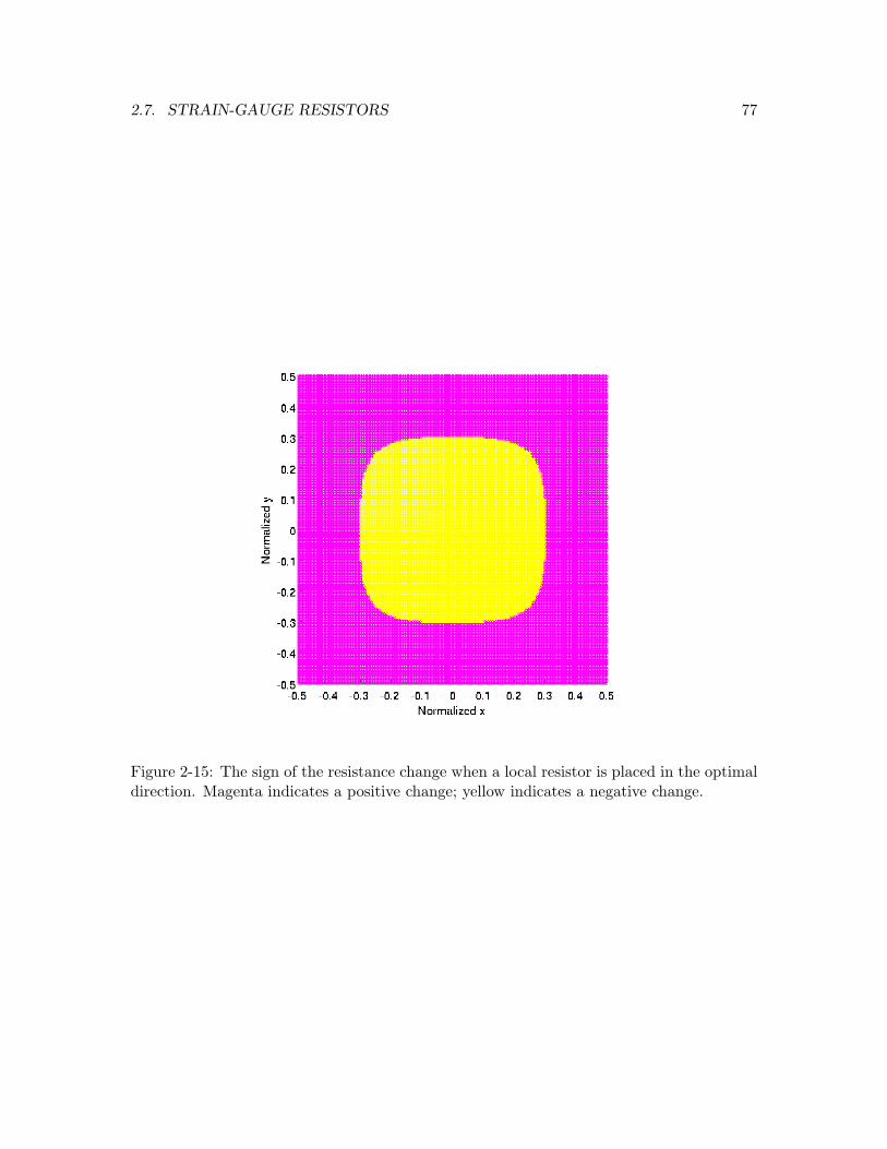
2.7. STRAIN-GAUGE RESISTORS 77
Figure 2-15: The sign of the resistance change when a local resistor is placed in the optimaldirection. Magenta indicates a positive change; yellow indicates a negative change.
78 CHAPTER 2. DEVICE DESIGN
optimal direction as suggested by Figure 2-14. Magenta indicates a positive change; yellow
indicates a negative change. This figure neatly divides the diaphragm into two regions:
a center area where the resistors oriented optimally would change positively, and a larger
ring area where the resistors oriented optimally would change opposingly. According to the
principle of the Wheatstone bridge as described in Section 2.4, we place two resistors in one
of these regions and two in the other.
2.7.3 Strain-gauge resistor pattern
Combining the insights from Figures 2-13, 2-14 and 2-15, we design four strain-gauge re-
sistors on a square diaphragm in the pattern shown in Figure 2-16. The design exhibits
odd symmetry about the center of the diaphragm, i.e. rotating it 180 yields an identical
pattern. The two resistors arranged in the center region change in the opposing direction
as the two resistors arranged closer to the edges of the diaphragm. All four resistors have
narrower lines (10 µm for a 2000 µm diaphragm), which yields higher resistances, near the
previously mentioned areas where absolute strain is high, and wider lines (20 µm) elsewhere.
For the Round 3 devices, which include diaphragms with lengths ranging from 1000 µm
to 4000 µm, the resistor dimensions are scaled accordingly. Since the ratios of lengths to
widths remains constant, the resistance is scale-invariant.
This novel snaking resistor design is unnecessary for most MEMS strain-gauge pressure
sensors, which concentrate resistance on the high-strain regions of the diaphragm because
the devices do not have wafer-scale conduction lines, but the additional resistance here more
than compensates for the loss in sensitivity.
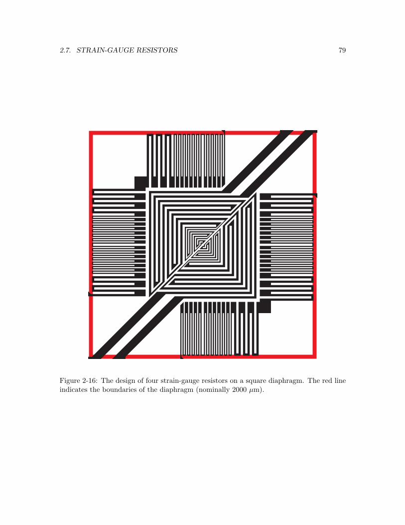
2.7. STRAIN-GAUGE RESISTORS 79
Figure 2-16: The design of four strain-gauge resistors on a square diaphragm. The red lineindicates the boundaries of the diaphragm (nominally 2000 µm).
80 CHAPTER 2. DEVICE DESIGN
2.8 Sensitivity
We estimate the maximum sensitivity of the strain-gauge pressure sensor, which, given the
voltage noise level, provides the pressure resolution. Suppose the resistors were concentrated
at the center of the edges of the diaphragm (locations CE), like those in the piezoresistive
pressure sensors discussed in Section 2.5 were. We calculate the strains using Equations 2.32
and 2.33 and diaphragm parameters L = 2000µm, H = 20µm, E = 169GPa and ν = 0.064:
ǫ⊥,CE =1
E(σ⊥,CE − νσ‖,CE) = (1.73× 10⁻⁸ Pa−1)P, (2.77)
ǫ‖,CE = 0. (2.78)
Thus, according to Equation 2.74, the relative changes in resistance for the resistors
with lengths oriented perpendicular and parallel to the diaphragm edge are
α⊥ = (2.19× 10⁻⁸ Pa−1)P, (2.79)
α‖ = (−1.27× 10⁻⁸ Pa−1)P, (2.80)
respectively, where a resistor Poisson’s ratio of νR = 0.21 is assumed.20 Applying these
values to the relationship between the output voltage and source voltage of a Wheatstone
bridge, shown in Equation 2.23 with α1 = α⊥ and α2 = α‖, we obtain
Vo
Vs≈ (1.73× 10⁻⁸ Pa−1)P, (2.81)
where we again assumed P ≪ 106 Pa. For a typical source voltage of 10 V, this corresponds
to a sensitivity of 0.173µV/Pa for resistors concentrated at the edge centers. The use of less
sensitive areas of the diaphragm reduces the sensitivity of the strain-gauge pressure sensors
by a factor of approximately 2, or down to 0.087 µV/Pa, which is much less sensitive than
the 19.0 µV/Pa for the piezoresistive pressure sensor analyzed in Section 2.5.
20This is the Poisson’s ratio of chromium, which was the primary material used to fabricate resistors forthis thesis.
2.8. SENSITIVITY 81
Thermal noise voltage is on the order of
VN ≈√
4kTRf, (2.82)
where k is Boltzmann’s constant, T is temperature, R is resistance, and f is the frequency.
Thus, for T = 300K, R = 10 kΩ, and a filtered bandwidth of f = 100Hz, the thermal
noise voltage is approximately 0.13 µV. Therefore, the pressure resolution is on the order of
1.5 Pa. As discussed earlier in Chapter 1, object detection and identification requires only
10 Pa resolution, so the strain-gauge pressure sensor is sufficiently sensitive for undersea
applications.
82 CHAPTER 2. DEVICE DESIGN
2.9 Dynamics
Estimates of the dynamics of the pressure sensor system are shown below. As a first pass,
the resonant frequency, or the frequency of the lowest mode of vibration, of the diaphragm
can be estimated by modeling the diaphragm as an ideal mass-spring system. We shall
consider the oscillatory behavior of an infinitesimal square portion of the diaphragm of size
dL× dL at the center of the diaphragm.
The system mass is best modeled as the total displaced mass. Strictly speaking, this
mass is the sum of the mass of the diaphragm plus the mass of the water displaced by the
flexing of the diaphragm. However, since the diaphragm is much thicker (20 µm) than the
maximum vertical displacement of water21 and silicon is denser than water, the mass of the
displaced water is negligible. The mass is the density of silicon times the volume of the
diaphragm:
dm = ρ dV (2.83)
= 2.3290 g/cm3 × 20µm× dL2 (2.84)
= 0.0469 kg/m2 × dL2. (2.85)
According to Hooke’s Law,
dF = dk · c1 = P dA, (2.86)
where dF is the applied force on the infinitesimal portion of the diaphragm, dk is its spring
constant, c1 is the displacement, P is the applied pressure, and dA = dL2 is the area, the
spring constant is
dk =P dA
c1. (2.87)
From the relationship between c1 and P shown in Equation 2.51 on Page 68, we obtain
P
c1=
EH3
KE(1− ν2)L4, (2.88)
21At a ratio of 0.188 nm/Pa, even 10,000 Pa of pressure only displaces water by 1.88 µm.
2.9. DYNAMICS 83
which yields a spring constant of
dk =EH3
KE(1− ν2)L4dL2 = 5.32× 10⁹N/m3 × dL2. (2.89)
The resonant frequency of a mass-spring system is
f =1
2π
√
dk
dm. (2.90)
Substituting the values from Equations 2.85 and 2.89 produces a resonant frequency
f = 54 kHz. (2.91)
A better approximation of the resonant frequency can be made using [3]
f = 1.654
√
E
ρ(1− ν2)
H
L2, (2.92)
which produces
f = 71 kHz. (2.93)
Since we are interested in pressure wave frequencies far less than this value, mechanically
filtering high frequency signals enable us to ignore the dynamic effects of the resonant
behavior of the diaphragms. The constricted channels that connect the cavities beneath
the diaphragm to the environment act as the desired mechanical lowpass filters.
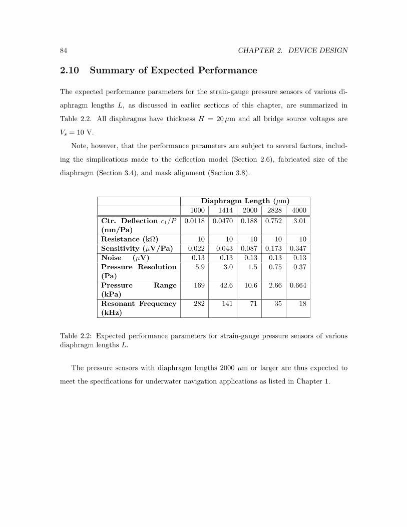
84 CHAPTER 2. DEVICE DESIGN
2.10 Summary of Expected Performance
The expected performance parameters for the strain-gauge pressure sensors of various di-
aphragm lengths L, as discussed in earlier sections of this chapter, are summarized in
Table 2.2. All diaphragms have thickness H = 20µm and all bridge source voltages are
Vs = 10 V.
Note, however, that the performance parameters are subject to several factors, includ-
ing the simplications made to the deflection model (Section 2.6), fabricated size of the
diaphragm (Section 3.4), and mask alignment (Section 3.8).
Diaphragm Length (µm)
1000 1414 2000 2828 4000
Ctr. Deflection c1/P(nm/Pa)
0.0118 0.0470 0.188 0.752 3.01
Resistance (kΩ) 10 10 10 10 10
Sensitivity (µV/Pa) 0.022 0.043 0.087 0.173 0.347
Noise (µV) 0.13 0.13 0.13 0.13 0.13
Pressure Resolution(Pa)
5.9 3.0 1.5 0.75 0.37
Pressure Range(kPa)
169 42.6 10.6 2.66 0.664
Resonant Frequency(kHz)
282 141 71 35 18
Table 2.2: Expected performance parameters for strain-gauge pressure sensors of variousdiaphragm lengths L.
The pressure sensors with diaphragm lengths 2000 µm or larger are thus expected to
meet the specifications for underwater navigation applications as listed in Chapter 1.
Chapter 3
Fabrication
This chapter describes the fabrication of the sensors. Section 3.1 provides an overview of
the fabrication process flow for Round 4 devices. Section 3.2 describes how the process flows
for devices from Rounds 1, 2, 3a and 3b differ from that for Round 4 devices. Section 3.3
describes the standard photolithographic procedures used in the experiments. Sections 3.4
and 3.5 discuss KOH and Pyrex etching, respectively. Section 3.6 reviews the anodic bond-
ing of silicon and Pyrex wafers. Section 3.7 explains how the process flow was designed.
Section 3.8 describes the designs of the various masks.
Standard integrated circuit (IC) fabrication techniques were used. When processes
differed from common usage, or when special techniques were employed, they are explained
in greater detail. Chemical vapor deposition, oxidation, e-beam evaporation deposition and
spin-on processes were used to deposit uniform layers of material.
For reference, the chemical formulas for the common names and abbreviations used are
given in Appendix A. Key standard operating procedures (SOPs) used for the process flows
are given in Appendix B. Appendix C contains the complete process flows, specific recipes
and descriptions of machines used. Appendices D and E shows the masks and technical
diagrams of the various apparatus, respectively, used during fabrication.
All processing, except where noted otherwise, was done in the Technology Research Lab-
oratory (TRL) and Integrated Circuits Laboratory (ICL) facilities of the MIT Microsystems
Technology Laboratories (MTL).
85
86 CHAPTER 3. FABRICATION
3.1 Overview of Fabrication of Round 4 Devices
The process flow for Round 4 devices is described below. The variations on this fabrication
process for earlier rounds of devices are listed in Section 3.2. The process flow for Round 5
devices is described in Section 5.3.
The silicon-based sensors start with a Silicon-On-Insulator (SOI) wafer, which is com-
prised of a thin (20 µm) (100) silicon wafer (called the front-side, or device wafer) bonded
to a standard-thickness (650 µm) (100) silicon wafer (called the back-side, or handle wafer)
through a thin (less than 1µm) layer of silicon oxide, an electrically insulating material.
SOI wafers were chosen as the initial substrates because they are readily available with
front-sides ranging from less than one micron to tens of microns, the desired thicknesses for
the thin wafer to act as the pressure-sensing diaphragm.
First, silicon nitride is deposited on both sides of the SOI wafer. The front-side nitride
is then etched, using a photolithographically-defined etch mask and a reactive-ion etcher,
to expose most of the front-side thin silicon and leave a nitride ring at the outer portion of
the front-side. Next, silicon oxide is grown on the front-side to insulate the semiconducting
silicon from the resistors, which sit on the oxide. The back-side nitride is then etched to
open square windows in the shape of the diaphragms. Finally, the silicon is anisotropically
etched in potassium hydroxide (KOH), with the nitride and the original oxide acting as an
etch mask and an etch stop, respectively. The KOH etch results in the release of the square
silicon diaphragms suspended over open cavities.
A Pyrex wafer is used to close the open cavities. To do so, channels are etched into the
Pyrex wafer using hydrofluoric acid and a chromium-gold etch mask. The etched face of the
Pyrex wafer is its front-side and the clean reverse face is its back-side. After the SOI wafer
and the Pyrex wafer are anodically bonded together, resistors are etched into a metal film
deposited by thermal evaporation of the front-side. Finally, a thin layer of Parylene polymer
is deposited on the front-side to waterproof and electrically insulate the resistors from the
aqueous environment. Optionally, single pressure-sensing cells, or entire pressure-sensing
arrays, are separated from the bonded wafer pair by die sawing, and subsequently packaged

3.1. OVERVIEW OF FABRICATION OF ROUND 4 DEVICES 87
for testing.
A graphical representation of the process flow for Pyrex alone can be found in Sub-
section 3.5.2. A graphical representation of the remaining device process flow for Round
4 devices is presented below. Only graphics where the wafer shape or layers change are
shown; changes between cleaning steps are not depicted. The step numbers correspond to
the complete process flow shown in Appendix Section C.3.
15 Start with SOI wafer
Si
Ox
Si
16 Deposit nitride
Si
Nitride
Ox
Si
17–20 Remove some nitride from front-side, leaving a nitride ring on the outer portion
Si
Nitride
OxSi
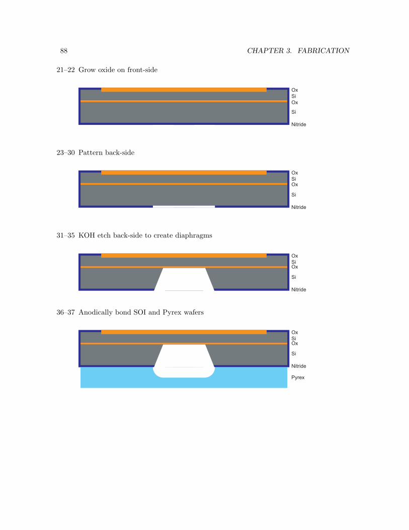
88 CHAPTER 3. FABRICATION
21–22 Grow oxide on front-side
Si
Nitride
Ox
Si
Ox
23–30 Pattern back-side
Si
Nitride
OxSi
Ox
31–35 KOH etch back-side to create diaphragms
Si
Nitride
OxSi
Ox
36–37 Anodically bond SOI and Pyrex wafers
Pyrex
Si
Nitride
OxSi
Ox
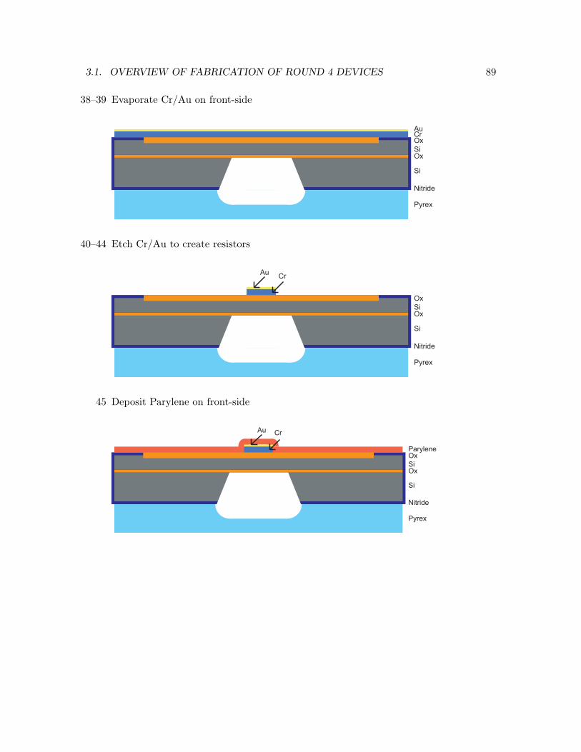
3.1. OVERVIEW OF FABRICATION OF ROUND 4 DEVICES 89
38–39 Evaporate Cr/Au on front-side
Pyrex
Si
Nitride
OxSi
OxCrAu
40–44 Etch Cr/Au to create resistors
Pyrex
Si
Nitride
OxSi
Ox
CrAu
45 Deposit Parylene on front-side
Pyrex
Si
Nitride
OxSi
OxParylene
CrAu

90 CHAPTER 3. FABRICATION
3.2 Variations on Fabrication for Rounds 1, 2, 3a and 3b
The differences between the process flows for devices from Rounds 1, 2, 3a and 3b and the
process flow for Round 4 devices are listed below. These are summarized in Table 3.1 at
the end of this section.
Truncated process flow
• Round 1 devices do not have resistors; the process flow ends at Step 37. Furthermore,
the front-side nitride is not etched and insulating oxide is not grown.
• Round 2 devices consist of resistors on dummy wafers. Fabrication consists solely of
Steps 38–44 performed on dummy silicon nitride wafers.
• Round 3a and 3b devices do not have a waterproofing Parylene layer; the process flow
ends at Step 43.
• Only Round 4 devices have a gold-on-chromium (Au-on-Cr) double-layer metal film
as the resistors. Devices from Rounds 1, 2, 3a and 3b have only chromium as the
resistor material. The reason for adding the gold is discussed in Section 4.4.
Extra steps that were later removed
• Round 1 and 3a devices have an additional KOH etch step at the beginning of the
process flow after nitride is deposited in order to find the crystalline plane. This
procedure can be found in Appendix Section C.2. The reason this step was later
discarded is discussed in Subsection 3.4.2.
• Round 1 devices have an additional step before silicon-Pyrex bonding: The nitride
envelope, including the back-side nitride, is completely stripped from the SOI wafer
in hot phosphoric acid. As discussed later in Section 3.6, this step was found to be
unnecessary and was thus discarded for subsequent rounds.
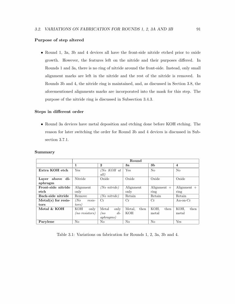
3.2. VARIATIONS ON FABRICATION FOR ROUNDS 1, 2, 3A AND 3B 91
Purpose of step altered
• Round 1, 3a, 3b and 4 devices all have the front-side nitride etched prior to oxide
growth. However, the features left on the nitride and their purposes differed. In
Rounds 1 and 3a, there is no ring of nitride around the front-side. Instead, only small
alignment marks are left in the nitride and the rest of the nitride is removed. In
Rounds 3b and 4, the nitride ring is maintained, and, as discussed in Section 3.8, the
aforementioned alignments marks are incorporated into the mask for this step. The
purpose of the nitride ring is discussed in Subsection 3.4.3.
Steps in different order
• Round 3a devices have metal deposition and etching done before KOH etching. The
reason for later switching the order for Round 3b and 4 devices is discussed in Sub-
section 3.7.1.
Summary
Round
1 2 3a 3b 4
Extra KOH etch Yes (No KOH atall)
Yes No No
Layer above di-aphragm
Nitride Oxide Oxide Oxide Oxide
Front-side nitrideetch
Alignmentonly
(No nitride) Alignmentonly
Alignment +ring
Alignment +ring
Back-side nitride Remove (No nitride) Retain Retain Retain
Metal(s) for resis-tors
(No resis-tors)
Cr Cr Cr Au-on-Cr
Metal & KOH KOH only(no resistors)
Metal only(no di-aphragms)
Metal, thenKOH
KOH, thenmetal
KOH, thenmetal
Parylene No No No No Yes
Table 3.1: Variations on fabrication for Rounds 1, 2, 3a, 3b and 4.

92 CHAPTER 3. FABRICATION
3.3 Photolithography
All photolithography was performed with the following tools, which can achieve feature
sizes and alignment accuracies under 1 µm.
• Coater: Manual Photoresist Coater Solitec Inc., Model 5110.
• EV1: Electronics Visions Model EV620 Mask Aligner.
• Developing Station: Semifab Model WPS 800 Wet Processing Station.
Two positive photoresists (PR) were used:
• AZ 917: Default PR on blank glass-chromium masks.
• OCG 934: PR for all other photolithographic steps.
Appendix Section C.1 contains the process flow for all photolithography steps. Appendix
Sections B.1 and B.2 describe the mask-making and photolithography standard operating
procedures, respectively, in detail.
Figure 3-1 depicts the procedure for transferring the features from a glass-chromium
mask to the photoresist on a substrate wafer. Each mask is a square 7” by 7” glass plate
with the intended pattern etched onto a thin chromium film on one face of the plate. The
mask is loaded chromium-side down into EV1. The wafer, spin-coated with photoresist on
one or both sides, is loaded into EV1 such that the chromium side of the mask is 30 µm
above the photoresist layer. The wafer is exposed to 365-405 nm wavelength ultraviolet
(UV) light through the mask for 2.3 seconds.
Since UV light cannot pass through chromium, the areas of the resist directly below
any chromium are left unchanged. Sensitizer materials in the exposed resist below open
regions of the mask, however, are broken down by the UV light. Once the wafer is placed
in a developer bath, the exposed photoresist washes away, revealing the original substrate.
Thus, the pattern in the mask is now transferred to the photoresist.
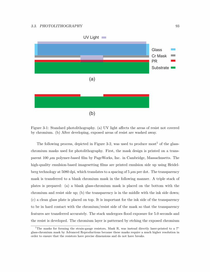
3.3. PHOTOLITHOGRAPHY 93
(a)
Glass
Substrate
(b)
UV Light
Cr Mask
PR
Figure 3-1: Standard photolithography. (a) UV light affects the areas of resist not coveredby chromium. (b) After developing, exposed areas of resist are washed away.
The following process, depicted in Figure 3-2, was used to produce most1 of the glass-
chromium masks used for photolithography. First, the mask design is printed on a trans-
parent 100 µm polymer-based film by PageWorks, Inc. in Cambridge, Massachusetts. The
high-quality emulsion-based imagesetting films are printed emulsion side up using Heidel-
berg technology at 5080 dpi, which translates to a spacing of 5 µm per dot. The transparency
mask is transferred to a blank chromium mask in the following manner. A triple stack of
plates is prepared: (a) a blank glass-chromium mask is placed on the bottom with the
chromium and resist side up; (b) the transparency is in the middle with the ink side down;
(c) a clean glass plate is placed on top. It is important for the ink side of the transparency
to be in hard contact with the chromium/resist side of the mask so that the transparency
features are transferred accurately. The stack undergoes flood exposure for 5.0 seconds and
the resist is developed. The chromium layer is patterned by etching the exposed chromium
1The masks for forming the strain-gauge resistors, Mask R, was instead directly laser-printed to a 7”glass-chromium mask by Advanced Reproductions because these masks require a much higher resolution inorder to ensure that the resistors have precise dimensions and do not have breaks.
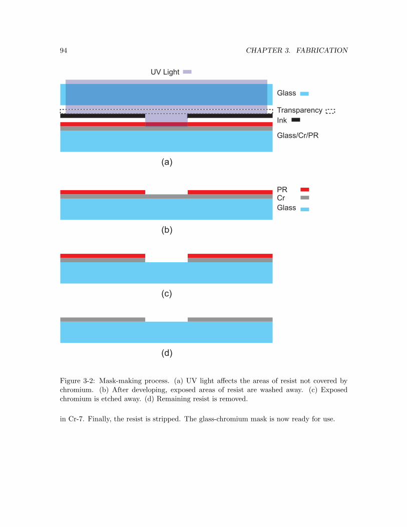
94 CHAPTER 3. FABRICATION
(a)
Glass
Transparency
Glass/Cr/PR
(b)
(c)
(d)
UV Light
Ink
Glass
CrPR
Figure 3-2: Mask-making process. (a) UV light affects the areas of resist not covered bychromium. (b) After developing, exposed areas of resist are washed away. (c) Exposedchromium is etched away. (d) Remaining resist is removed.
in Cr-7. Finally, the resist is stripped. The glass-chromium mask is now ready for use.
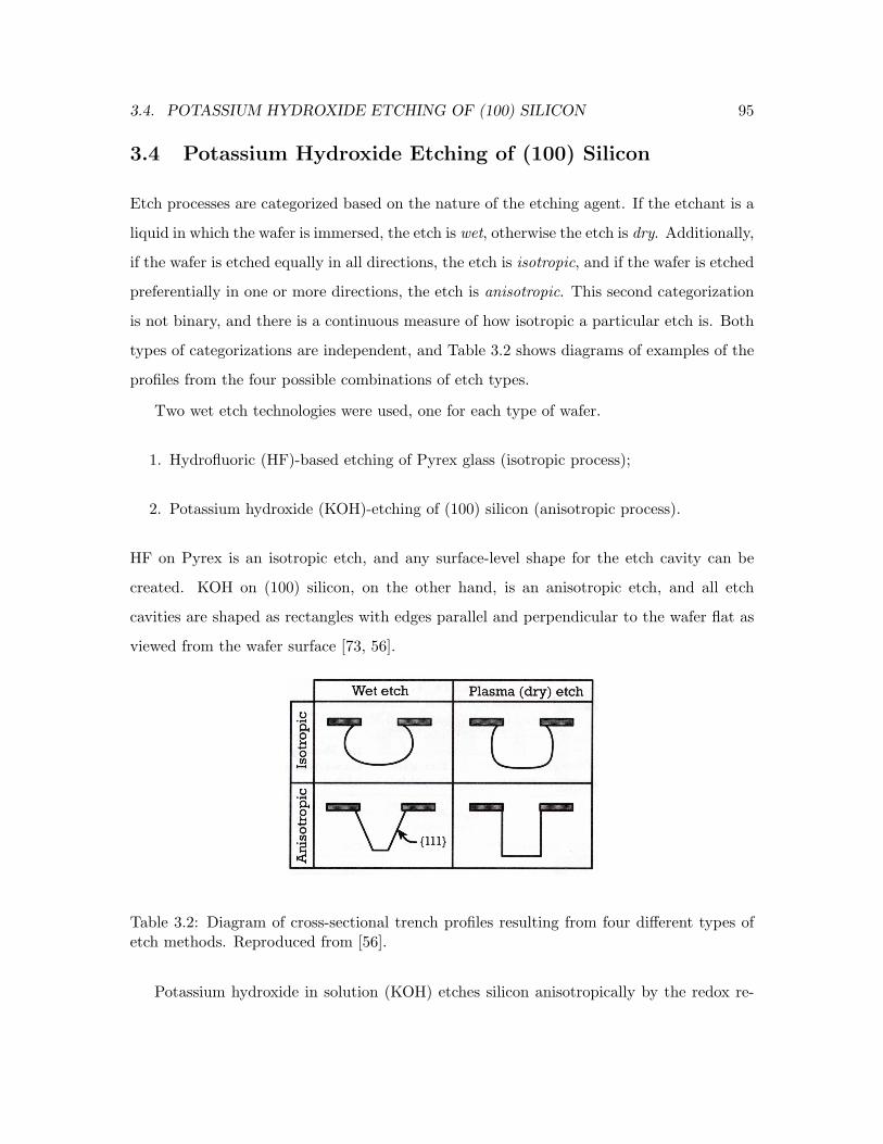
3.4. POTASSIUM HYDROXIDE ETCHING OF (100) SILICON 95
3.4 Potassium Hydroxide Etching of (100) Silicon
Etch processes are categorized based on the nature of the etching agent. If the etchant is a
liquid in which the wafer is immersed, the etch is wet, otherwise the etch is dry. Additionally,
if the wafer is etched equally in all directions, the etch is isotropic, and if the wafer is etched
preferentially in one or more directions, the etch is anisotropic. This second categorization
is not binary, and there is a continuous measure of how isotropic a particular etch is. Both
types of categorizations are independent, and Table 3.2 shows diagrams of examples of the
profiles from the four possible combinations of etch types.
Two wet etch technologies were used, one for each type of wafer.
1. Hydrofluoric (HF)-based etching of Pyrex glass (isotropic process);
2. Potassium hydroxide (KOH)-etching of (100) silicon (anisotropic process).
HF on Pyrex is an isotropic etch, and any surface-level shape for the etch cavity can be
created. KOH on (100) silicon, on the other hand, is an anisotropic etch, and all etch
cavities are shaped as rectangles with edges parallel and perpendicular to the wafer flat as
viewed from the wafer surface [73, 56].
Table 3.2: Diagram of cross-sectional trench profiles resulting from four different types ofetch methods. Reproduced from [56].
Potassium hydroxide in solution (KOH) etches silicon anisotropically by the redox re-
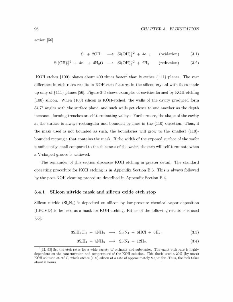
96 CHAPTER 3. FABRICATION
action [56]
Si + 2OH− −→ Si(OH)+22 + 4e−, (oxidation) (3.1)
Si(OH)+22 + 4e− + 4H2O −→ Si(OH)−2
6 + 2H2. (reduction) (3.2)
KOH etches 100 planes about 400 times faster2 than it etches 111 planes. The vast
difference in etch rates results in KOH-etch features in the silicon crystal with faces made
up only of 111 planes [56]. Figure 3-3 shows examples of cavities formed by KOH-etching
(100) silicon. When (100) silicon is KOH-etched, the walls of the cavity produced form
54.7 angles with the surface plane, and such walls get closer to one another as the depth
increases, forming trenches or self-terminating valleys. Furthermore, the shape of the cavity
at the surface is always rectangular and bounded by lines in the 〈110〉 direction. Thus, if
the mask used is not bounded as such, the boundaries will grow to the smallest 〈110〉-
bounded rectangle that contains the mask. If the width of the exposed surface of the wafer
is sufficiently small compared to the thickness of the wafer, the etch will self-terminate when
a V-shaped groove is achieved.
The remainder of this section discusses KOH etching in greater detail. The standard
operating procedure for KOH etching is in Appendix Section B.3. This is always followed
by the post-KOH cleaning procedure described in Appendix Section B.4.
3.4.1 Silicon nitride mask and silicon oxide etch stop
Silicon nitride (Si3N4) is deposited on silicon by low-pressure chemical vapor deposition
(LPCVD) to be used as a mask for KOH etching. Either of the following reactions is used
[66]:
3SiH2Cl2 + 4NH3 −→ Si3N4 + 6HCl + 6H2, (3.3)
3SiH4 + 4NH3 −→ Si3N4 + 12H2. (3.4)
2[92, 93] list the etch rates for a wide variety of etchants and substrates. The exact etch rate is highlydependent on the concentration and temperature of the KOH solution. This thesis used a 20% (by mass)KOH solution at 80C, which etches (100) silicon at a rate of approximately 80 µm/hr. Thus, the etch takesabout 8 hours.
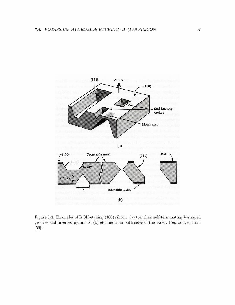
3.4. POTASSIUM HYDROXIDE ETCHING OF (100) SILICON 97
Figure 3-3: Examples of KOH-etching (100) silicon: (a) trenches, self-terminating V-shapedgrooves and inverted pyramids; (b) etching from both sides of the wafer. Reproduced from[56].
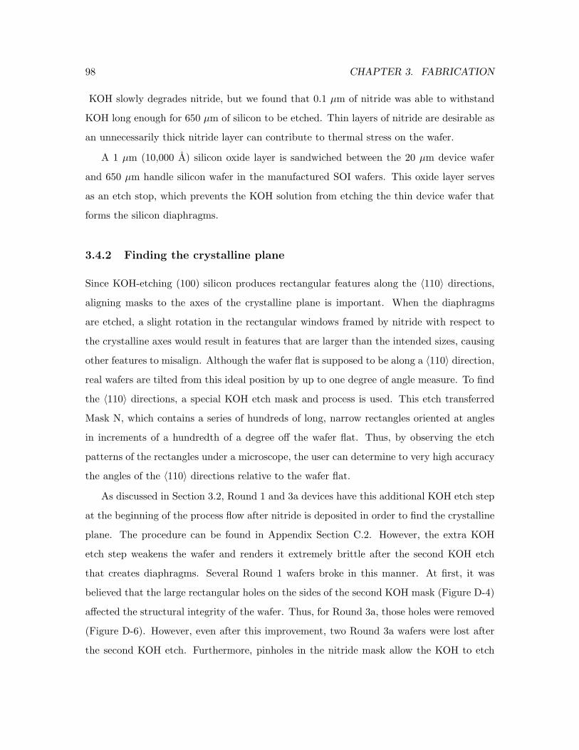
98 CHAPTER 3. FABRICATION
KOH slowly degrades nitride, but we found that 0.1 µm of nitride was able to withstand
KOH long enough for 650 µm of silicon to be etched. Thin layers of nitride are desirable as
an unnecessarily thick nitride layer can contribute to thermal stress on the wafer.
A 1 µm (10,000 A) silicon oxide layer is sandwiched between the 20 µm device wafer
and 650 µm handle silicon wafer in the manufactured SOI wafers. This oxide layer serves
as an etch stop, which prevents the KOH solution from etching the thin device wafer that
forms the silicon diaphragms.
3.4.2 Finding the crystalline plane
Since KOH-etching (100) silicon produces rectangular features along the 〈110〉 directions,
aligning masks to the axes of the crystalline plane is important. When the diaphragms
are etched, a slight rotation in the rectangular windows framed by nitride with respect to
the crystalline axes would result in features that are larger than the intended sizes, causing
other features to misalign. Although the wafer flat is supposed to be along a 〈110〉 direction,
real wafers are tilted from this ideal position by up to one degree of angle measure. To find
the 〈110〉 directions, a special KOH etch mask and process is used. This etch transferred
Mask N, which contains a series of hundreds of long, narrow rectangles oriented at angles
in increments of a hundredth of a degree off the wafer flat. Thus, by observing the etch
patterns of the rectangles under a microscope, the user can determine to very high accuracy
the angles of the 〈110〉 directions relative to the wafer flat.
As discussed in Section 3.2, Round 1 and 3a devices have this additional KOH etch step
at the beginning of the process flow after nitride is deposited in order to find the crystalline
plane. The procedure can be found in Appendix Section C.2. However, the extra KOH
etch step weakens the wafer and renders it extremely brittle after the second KOH etch
that creates diaphragms. Several Round 1 wafers broke in this manner. At first, it was
believed that the large rectangular holes on the sides of the second KOH mask (Figure D-4)
affected the structural integrity of the wafer. Thus, for Round 3a, those holes were removed
(Figure D-6). However, even after this improvement, two Round 3a wafers were lost after
the second KOH etch. Furthermore, pinholes in the nitride mask allow the KOH to etch
3.4. POTASSIUM HYDROXIDE ETCHING OF (100) SILICON 99
small pyramidal dimples on the surface, making it difficult for other fabrication tools to
clamp onto the back-side silicon by vacuum suction. Since the plane-finding KOH etch
would occur early in the fabrication process to align subsequent masks to the crystalline
plane, future processing steps are affected.3
In the end, however, the 〈110〉 directions were found to be sufficiently close to the wafer
flat that the crystalline-finding KOH etch was not necessary. Due to the risks with wafer
weakening and back-side suction discussed above (not to mention the additional time spent
with photolithography, etching, cleaning and observing), this step is not worth taking. Thus,
the process flows for Rounds 3b and 4 discard the crystalline-finding KOH etch step. These
rounds assume the SOI wafer flat is parallel to a 〈110〉 direction.
3.4.3 Mechanical wafer protection
Because protective nitride is removed from, and insulating oxide is grown on, the front-side
of the SOI wafer before KOH etching the back-side silicon (the rationale for this is discussed
in Subsection 3.7.2), KOH etching is done with special care. The KOH solution envelopes
the entire wafer, etching any region, both silicon and oxide (albeit at different rates), that
is unprotected by nitride.
To protect the front-side device wafer, the wafer is placed inside a custom-made KOH
wafer holder that only allows one side of the wafer to be exposed to the KOH solution
(Figure 3-4). The wafer holder, which holds one wafer at a time, is a circular apparatus
made of polytetrafluoroethylene (PTFE). It consists of a bottom plate and a top ring both
with grooves to hold O-rings of diameters slightly smaller than that of the wafer. The wafer
is sandwiched between the O-rings of the bottom plate and top ring back-side up, and the
whole assembly is held together by 12 screws. When the loaded apparatus is placed in the
KOH solution, the top O-ring prevents KOH solution from seeping to the edge of the wafer.
As a secondary precaution, even if some KOH solution leaks through the top O-ring, the
bottom O-ring prevents KOH solution from reaching the protected wafer side.
3Note that this is not an issue for the KOH etch that creates the diaphragms. The silicon wafer is bondedto Pyrex immediately after that etch, and subsequent processing handles the clean back-side of the Pyrexwafer.
100 CHAPTER 3. FABRICATION
Figure 3-4: Side view of KOH wafer holder. The wafer is placed front-side down to exposethe back-side to KOH. The black circles represent the cross-section of the O-rings. Onlythe exposed silicon comes into contact with KOH solution, which surrounds the apparatus,and the oxide layer (violet) is protected.
Figures E-1, E-2 and E-3 in Appendix E depict the technical diagrams of the KOH wafer
holder from the top and bottom views.
Use of the wafer holder requires special care. Uneven stress from the mounting screws
can cause the wafer to crack. Thus, in order to ensure that the wafer is loaded under
uniform stress, the user tightens the 12 screws gradually by only turning each screw a few
rotations before moving on to a screw at the opposite end of the wafer holder, much like
installing an automobile tire. Additionally, the wafer is first rinsed after the KOH etch
while still loaded in the wafer holder. Even after this rinse, some KOH solution may still
be lodged between the O-rings and the wafer. Thus, a second 15-minute cascade rinse on
the bare wafer out of the holder removes any residual KOH.
As discussed in Section 3.2, in Rounds 1 and 3a, there is no ring of nitride on the front-
side of the device wafer. Instead, the front-side is all oxide. Thus, if some KOH solution
manages to leak through the top O-ring, it would begin to attack the oxide outside the
bottom O-ring. Although silicon oxide can serve as an etch stop for KOH, it does not hold
up against KOH as well as nitride does: Since the grown front-side oxide is only 0.1 µm
(1000 A) thick,4 it would take less than an hour for the KOH to etch through completely at
4In contrast, the oxide etch stop sandwiched between the device and handle wafers is 1 µm (10,000 A)thick.

3.4. POTASSIUM HYDROXIDE ETCHING OF (100) SILICON 101
a rate of approximately 20 A/min. Furthermore, once some oxide is etched, the KOH can
tunnel under the bottom O-ring to reach the device portion of the oxide layer. In one Round
3a wafer, this leakage did indeed occur, rendering the wafer unusable. Thus, in Rounds 3b
and 4, a ring of front-side nitride is maintained to serve as a second line of defense in case
the top O-ring doesn’t perfectly block KOH.
As mentioned earlier in Subsection 2.2.4, Round 3b wafers further differed from Round
3a wafers in that the four sensors at the corners of the wafer were removed. Those the back-
side nitride windows that create those diaphragms happen to overlap with the top O-ring.
Thus, as the cavity directly in contact with the O-ring is etched in the KOH solution, the
solution is able to tunnel under the top O-ring and possibly attack some of the oxide on
the other side of the wafer. When this effect was discovered, the masks were corrected by
removing those four sensors.
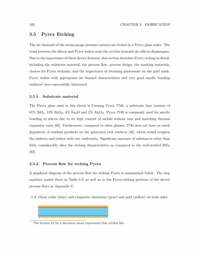
102 CHAPTER 3. FABRICATION
3.5 Pyrex Etching
The air channels of the strain-gauge pressure sensors are etched in a Pyrex glass wafer. The
bond between the silicon and Pyrex wafers seals the cavities beneath the silicon diaphragms.
Due to the importance of these device features, this section describes Pyrex etching in detail,
including the substrate material, the process flow, process design, the masking materials,
choices for Pyrex etchants, and the importance of retaining photoresist on the gold mask.
Pyrex wafers with appropriate air channel characteristics and very good anodic bonding
surfaces5 were successfully fabricated.
3.5.1 Substrate material
The Pyrex glass used in this thesis is Corning Pyrex 7740, a substrate that consists of
81% SiO2, 13% B2O3, 4% Na2O and 2% Al2O3. Pyrex 7740 is commonly used for anodic
bonding to silicon due to its high content of mobile sodium ions and matching thermal
expansion rates [92]. Furthermore, compared to other glasses, 7740 does not have as much
deposition of residual products on the generated etch surfaces [48], which would roughen
the surfaces and reduce etch rate uniformity. Significant amounts of substances other than
SiO2 considerably alter the etching characteristics as compared to the well-studied SiO2
[92].
3.5.2 Process flow for etching Pyrex
A graphical diagram of the process flow for etching Pyrex is summarized below. The step
numbers match those in Table 3.3, as well as in the Pyrex-etching portions of the device
process flows in Appendix C.
1–6 Clean wafer (blue) and evaporate chromium (gray) and gold (yellow) on both sides
5See Section 3.6 for a discussion about experiments that verified this.
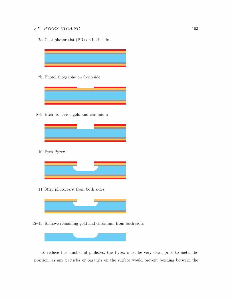
3.5. PYREX ETCHING 103
7a Coat photoresist (PR) on both sides
7b Photolithography on front-side
8–9 Etch front-side gold and chromium
10 Etch Pyrex
11 Strip photoresist from both sides
12–13 Remove remaining gold and chromium from both sides
To reduce the number of pinholes, the Pyrex must be very clean prior to metal de-
position, as any particles or organics on the surface would prevent bonding between the

104 CHAPTER 3. FABRICATION
Table 3.3: Process flow for etching Pyrex wafers. It can also be found in Appendix C aspart of the complete process flows for device fabrication.
Step Lab Machine Recipe Description
1 Clean TRL Acid hood Standard Clean Pyrex wafers with 10 minpiranha and 15 s 50:1 HF dip
2 Clean TRL Asher Standard Clean wafers by ashing organics(optional)
3 Metal TRL E-beam Standard Evaporate 200 A Cr then 1000A Au on front-side
4 Clean TRL Acid hood Standard Clean wafers again with 10 minpiranha and 15 s 50:1 HF dip
5 Clean TRL Asher Standard Clean wafers again by ashing or-ganics (optional)
6 Metal TRL E-beam Standard Evaporate 200 A Cr then 1000A Au on back-side
7 Photo (front) TRL Coater/EV1 Standard (double-sided)
Mask P (Pyrex features) withback-side protection
8 Etch TRL Acid hood 28 A/s Etch Au with gold etchant TFAor aqua regia
9 Etch TRL Acid hood 25 A/s Etch Cr with Cr-7
10 Etch TRL Acid hood 0.8 µm/min Etch Pyrex with 660:140:200H2O:HNO3:HF
11 Strip TRL Acid hood Standard Strip PR
12 Strip TRL Acid hood 25 A/s Remove remaining Au with goldetchant TFA or aqua regia
13 Strip TRL Acid hood 28 A/s Remove remaining Cr with Cr-7
14 Storage TRL — — Save the Pyrex wafers for laterprocessing
3.5. PYREX ETCHING 105
Pyrex and metal. There is much work reported in the literature regarding cleaning glass
surfaces for adhesion [1, 13]. For this thesis, the following cleaning procedure was used.
First, the Pyrex is placed in freshly prepared piranha (3:1 H2SO4:H2O2) for 10 minutes at
120C, which removes organic matter. After the wafers are rinsed in distilled water, they
are dipped in 50:1 H2O:49% HF for 15 seconds, etching the Pyrex by a microscopic amount
to undercut any remaining particles. The wafer is then rinsed thoroughly to remove all HF
and then spun dry. If desired, the wafer may then be ashed to further remove organics,
but in this thesis, this step was found to be unnecessary. It should also be noted that this
cleaning process assumes the Pyrex is already in the clean condition as prepared by the
manufacturer. If it is not, then other steps should be taken prior to the piranha clean.
Immediately after the wafer is cleaned, the wafer is placed in the metal mask deposition
machine. An electron beam evaporator was used to deposit chromium and gold; the metals
were deposited in succession in the same vacuum. 200 A of Cr and 1000 A of Au are
sufficient. Thicker metal layers act as better masks, but the improvement may not be
worth the higher fabrication costs. A slower deposition rate generally produces a more
uniform thickness across the wafer. A deposition rate of 3 A/s was used for both metals.
It is important for the two metals to be deposited in immediate succession. Exposing the
chromium surface to air would enable chromium oxide (CrO) to form, which etches in
the Pyrex etchants. Although the standard operating procedure for the machine calls for a
pressure of 2.0×10⁻⁶ Torr (or mmHg), much lower vacuum pressures in the range 1.9×10⁻⁷
to 2.7 × 10⁻⁷ Torr was used. The higher-quality vacuum creates a cleaner metal surface
since there are fewer extraneous particles in the space. This generally requires pumping
down the machine overnight. Since the e-beam evaporator only deposits on one side of a
wafer at a time, the wafer cleaning and metal deposition processes are then repeated for the
other side of the wafer. Gold scratches easily, so it is very important to ensure that solid
tools do not unnecessarily touch the metal surface in all subsequent steps.
Once the metal mask has been prepared, standard double-sided photolithography with
a photoresist thickness of 1 µm is done. As usual, photoresist is first spun on the side
that will not be etched (back-side). Although the integrity of the photoresist on the back-
106 CHAPTER 3. FABRICATION
side is generally not as crucial as the front-side, it should be noted that for some of the
process flows in this thesis, the Pyrex is later bonded to an SOI wafer and undergoes further
photolithography. Thus, the back-side Pyrex must be smooth enough after Pyrex etching
to provide even contact with the vacuum chuck of the spin steps. Since, for this thesis,
protecting the back-side is just as important as protecting the front-side, extra care is
taken to ensure that the spin coater is clean so that during front-side coating, the back-side
photoresist is not disturbed. As a further precaution, extra photoresist can be brushed on
the back-side by hand, but this was not done in this thesis.
Next, the pattern from the photoresist is etched into gold. There are two choices of gold
etchants:
• Gold etchant thin film type A (TFA): 30% potassium iodide (KI), 1.3% iodine (I2),
68.7% water (H2O);
• Aqua regia: 3 hydrochloric acid (HCl) : 1 nitric acid (HNO3).
Either choice was found to be suitable. The wafer is thoroughly rinsed and then the
chromium is etched in Cr-7 (9% (NH4)2Ce(NO3)6 + 6%HClO4 +H2O). The wafer is thor-
oughly rinsed again. The gold etchant does not etch the photoresist and Cr-7 etches neither
the photoresist nor the gold. The wafer should be removed from the etchants as soon as
possible, as over-etching will cause undercutting of the metal masks.
The wafer is now ready for Pyrex etching. A solution of 660:140:200 H2O:HNO3:HF is
prepared. The wafer is placed in the solution for a timed etch front-side up so that bubbles
do not collect on the etching surface. It should be noted that during the metal and Pyrex
etching, the sides of the wafers are completely bare. Furthermore, since the wafer sits on a
narrow rim in the e-beam evaporator, a 1-mm wide rim on the outside of the wafer is left
without metal on either side as well. Thus, the edges of the Pyrex are etched away. This
effect should be taken into account for mask design if the features run to the edge.
The wafer is then thoroughly rinsed. The masks (photoresist, gold, chromium) are then
successively removed. This completes the Pyrex etching process.
3.5. PYREX ETCHING 107
3.5.3 Process design for etching Pyrex
The process described in the previous subsection was developed after a literature review and
experiments that explored the various masks materials and wet etchants were conducted.
The results of this research is discussed in the remainder of this section on Pyrex etching.
There are several choices for etching types and recipes, all with various advantages
and disadvantages. To pick the most appropriate process, the following specifications were
considered. The etch should be fast enough so that channels of depth 50 µm to 100 µm
can be etched in a reasonable amount of time, but not so fast as to result in unreliable or
inconsistent features. The etch mask must be strong enough to prevent the formation of
extraneous canals that would connect channels together at undesired locations. The surface
must remain smooth enough to anodically bond with silicon. Other requirements, such as
sidewall smoothness, high uniformity and isotropicity, are not important for this thesis.
3.5.4 Masking materials
All the wet Pyrex etchants lift off a photoresist layer spun directly on Pyrex because pho-
toresist does not adhere strongly enough to Pyrex. Fortunately, photoresist adheres well
to metal, so metal masks, in place of phororesist, are necessary to etch Pyrex successfully.
A successful mask must satisfy four conditions: (1) it does not cause damage to the Pyrex
substrate during its deposition; (2) it can be etched with photoresist as an etch mask; (3)
it can stand up to the Pyrex etchant; and (4) it leaves the Pyrex surface smooth after
its removal. Although several silicon-based materials, such as amorphous silicon, polysili-
cion, bulk silicon and silicon carbide, are possible and have been reported in the literature
[88, 80, 49, 48, 5], this thesis used a multilayer metal film as the mask for etching Pyrex.
Since gold is an inert material in all the wet etchants considered, it was used as the etch
mask, with an adhesion layer of chromium deposited between the Pyrex wafer and the gold
layer [5]. Table 1 in [48] provides an overview of various masking materials.
The success of an etch is extremely sensitive to the quality of the metal masks. Since
wet Pyrex etches are nearly isotropic, a microscopic pinhole in the metal masks will lead to
a hemispheric dimple in the Pyrex. If there are sufficiently many pinholes, then not only
108 CHAPTER 3. FABRICATION
is the quality of the bonding surface compromised, but such dimples can merge with one
another and create unwanted canals between the etched channels. Another type of defect
is notching defects on the edges of the metal mask. Both pinholes and notching defects
can be caused by the tensile stress induced in the metal masks during the cooling process
after deposition. The cooling process creates creeps in the metal [80] as well as causes
freestanding metal to break as the metal is undercut during the isotropic Pyrex etch [49].
The Pyrex etchant seeps into these creeps and produces pinholes.
One way to reduce the stress is to anneal the metal; however, annealing can also diffuse
gold into the chromium layer, which reduces the efficacy of the mask. Annealing also has
the side effects of increasing the Pyrex etch rate due to a redistribution of oxides [49] and
roughing the etch surface [48].
In addition to protecting both sides of the Pyrex wafer during the wet Pyrex etch, the
double-sided metal layers also stabilize the stress characteristics of the wafer [80]. The
stress induced by the deposition on one side nearly cancels out that induced on the other
side. Thus, identical deposition procedures should be followed for both sides, as the stress
is dependent on the process parameters and equipment.
Because of the tensile stress from metal masks, some applications prefer a masking layer,
such as amorphous silicon or polysilicon, with compressive stress instead of tensile stress
[49]. Another advantage that silicon-based masks provide is a hydrophobic surface, which
causes pinholes and notches to repel wet Pyrex etchants. However, silicon-based masks are
comparatively more difficult to deposit and to remove with the tools available for this thesis
and were therefore not attempted. Furthermore, the surface of a metal mask can be made
sufficiently hydrophobic by leaving photoresist on it.
It has been reported that performing multiple (three or four) depositions of gold with a
cooling time of 30 minutes in between depositions reduces the number of pinholes [49], since
successive depositions cover the defects in the previous layer. Such masks are of very high
quality. However, this procedure was not used in this thesis since the number of pinholes
from a single metal deposition was sufficiently low for the desired application.
3.5. PYREX ETCHING 109
3.5.5 Pyrex etchants
There is a good selection of HF-based etchants for Pyrex available; an overview of their
mechanisms is given in [77]. When the author of this thesis was working on tunable
MEMS resonators, several preliminary experiments on wet-etching Pyrex were conducted
[46]. First, buffered oxide etch (BOE), a 5:1 mixture of 40% ammonium fluoride (NH4F)
and pure 49% hydrofluoric acid (HF)6, was used; it was found to etch too slowly. Thus, pure
49% HF was tested instead, but standard OCG photoresist could not withstand HF long
enough to serve as a mask. Furthermore, replacing OCG with an SU-8 polymer photoresist
did not solve this problem. Others have successfully studied deep etching of Pyrex in 49%
HF [80, 49], but due to safety concerns with highly concentrated HF, their processes were
not attempted. Finally, the etch solution 660:140:200 H2O:HNO3:HF, which has an etch
rate of approximately 0.8 µm/min, was found to work well. The nitric acid removes the
impurities from the Pyrex, and the HF etches the remaining SiO2.
3.5.6 Importance of retaining photoresist on gold
It is important to retain the photoresist layer over the gold layer during wet etching of
Pyrex. Although gold stands up to HF, BOE and the 660:140:200 H2O:HNO3:HF solution,
microscopic pinholes in the chromium and gold layers expose Pyrex to the etch solution,
which create unwanted hemispheric dimples on the wafer surface. By keeping the photoresist
over the metal layers during the Pyrex etch, the pinholes are covered. Highly concentrated
HF etchants will eventually lift off a photoresist layer, but the photoresist that fills in the
pinholes remain for a much longer period of time because of high adhesion to the cracks
and limited contact area with the etchant. Although some work reported hard-baking the
photoresist at 120C for 30 minutes [80], this was not found to be necessary.
Several experiments confirm that photoresist is necessary. First, the photoresist was
removed using piranha after gold was etched but before chromium and Pyrex are etched.
When the wafer was placed in Cr-7 to etch the chromium, the entire metal lifted off in large
pieces. Second, on another wafer, photoresist was removed using piranha after both gold
6“Pure 49% HF” is a solution that consists of 49% HF and 51% H2O by volume.
110 CHAPTER 3. FABRICATION
and chromium were etched but before Pyrex was etched. During Pyrex etching, the metal
lifted off on a microscale and numerous hemispheric dimples were etched into the Pyrex.
To summarize both experiments, removing photoresist before the Pyrex is etched causes
the metal mask to lift off in the etch step immediately following photoresist removal.
Problems with metalization and the effect of piranha on the metal can both be ruled out
as explanations for the results of the above two experiments. Wafers that were successfully
etched using the standard procedure were metalized at the same time under the same
conditions as the wafers used in the experiments. Also, all wafers have metal on one side
exposed to piranha. After metal has been deposited on one side, the wafers are cleaned
again in piranha and diluted HF in preparation for metal deposition on the other side.
A final experiment demonstrated that photoresist inside the pinholes is crucial. Re-
moving photoresist using acetone and isopropanol (IPA) instead of using piranha was done
as well. This procedure is not as thorough as a piranha strip, so the photoresist over the
microsized pinholes, which adheres much more strongly to the metal as compared to surface
photoresist, may not be completely removed. The removal was done prior to metal etching.
The metal mask was left intact after the entire etch process and the resulting wafer surface
was comparable to that of leaving the entire photoresist layer on during the Pyrex etch.
The hypothesis that photoresist remained on the metal is confirmed by the observation
that after gold etchant and Cr-7 were applied multiple times, numerous specks of metal,
protected by photoresist, remained. Others reported similar results [49].
3.6. ANODIC BONDING 111
3.6 Anodic Bonding
The silicon and Pyrex wafers are anodically bonded together to seal the air cavities beneath
the diaphragms and the air channels that connect the cavities. In this process, the wafers are
placed in contact with each other in a vacuum, heated to 350C and an electric potential of
1000 V is applied across the sandwich, with the silicon at the higher potential. The potential
induces migration of sodium ions from the Pyrex wafer into the silicon wafer, resulting in a
net negative charge for the Pyrex wafer, and a net positive charge in the silicon. The two
charged surfaces then are brought into intimate contact and the heat fuses the two wafers
together. The recipe for anodic bonding used in all device fabrication is given in Appendix
Section B.6.
As discussed in Section 3.2, Round 1 devices have an additional step before silicon-Pyrex
bonding: The nitride layer is completely stripped from the SOI wafer in hot phosphoric
acid.7 However, this is a violent procedure that frequently shatters wafers. Furthermore,
the dry etches used to remove nitride (such as for creating the nitride ring) are inappropriate
for back-side removal because they can roughen the silicon surface to the extent that an
air-tight bond with Pyrex cannot take place. In subsequent rounds of device fabrication,
nitride stripping was discarded, and Pyrex was successfully bonded to silicon wafers that
had the back-side nitride layer still intact. Thus, sodium ions can migrate through thin
nitride films on the surface of a silicon wafer.
An experiment demonstrated that the anodic bond is indeed air-tight. Recall that
Round 3a wafers have nine columns of ten devices each, where the cavities in the devices of
the same column are connected via air channels etched in Pyrex. There are no outlets to the
atmosphere. Before bonding one particular Round 3a wafer set, three of the nine columns
each had one diaphragm broken (thus allowing those cavities access to the environment),
and the other six columns had all their diaphragms intact. Since anodic bonding occurs in a
vacuum, an air-tight bond would deform the diaphragms of the six intact columns inwards.
Contrastingly, the diaphragms of the other three columns should remain flat. This is, in
fact, what was observed. Furthermore, when five of the six intact columns later had one
7The procedure is given in Appendix Section B.5.

112 CHAPTER 3. FABRICATION
diaphragm carefully broken, thus exposing the entire column to atmospheric pressure, the
other diaphragms in that column immediately popped back to their flat equilibrium state.
The last of the six columns was kept intact for several months without any of the diaphragms
popping back. This experiment also showed that the Pyrex etching process described in
Section 3.5 produces sufficiently few pinholes that the air channels do not have additional
etched canals to connect them.
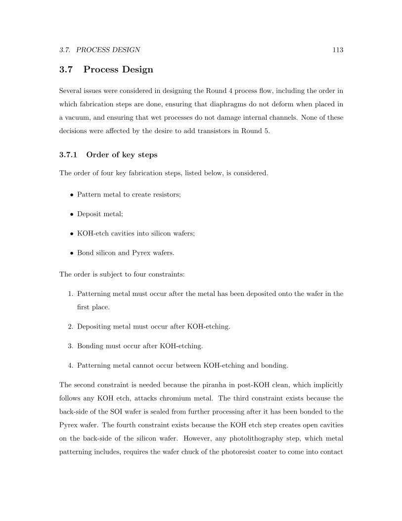
3.7. PROCESS DESIGN 113
3.7 Process Design
Several issues were considered in designing the Round 4 process flow, including the order in
which fabrication steps are done, ensuring that diaphragms do not deform when placed in
a vacuum, and ensuring that wet processes do not damage internal channels. None of these
decisions were affected by the desire to add transistors in Round 5.
3.7.1 Order of key steps
The order of four key fabrication steps, listed below, is considered.
• Pattern metal to create resistors;
• Deposit metal;
• KOH-etch cavities into silicon wafers;
• Bond silicon and Pyrex wafers.
The order is subject to four constraints:
1. Patterning metal must occur after the metal has been deposited onto the wafer in the
first place.
2. Depositing metal must occur after KOH-etching.
3. Bonding must occur after KOH-etching.
4. Patterning metal cannot occur between KOH-etching and bonding.
The second constraint is needed because the piranha in post-KOH clean, which implicitly
follows any KOH etch, attacks chromium metal. The third constraint exists because the
back-side of the SOI wafer is sealed from further processing after it has been bonded to the
Pyrex wafer. The fourth constraint exists because the KOH etch step creates open cavities
on the back-side of the silicon wafer. However, any photolithography step, which metal
patterning includes, requires the wafer chuck of the photoresist coater to come into contact
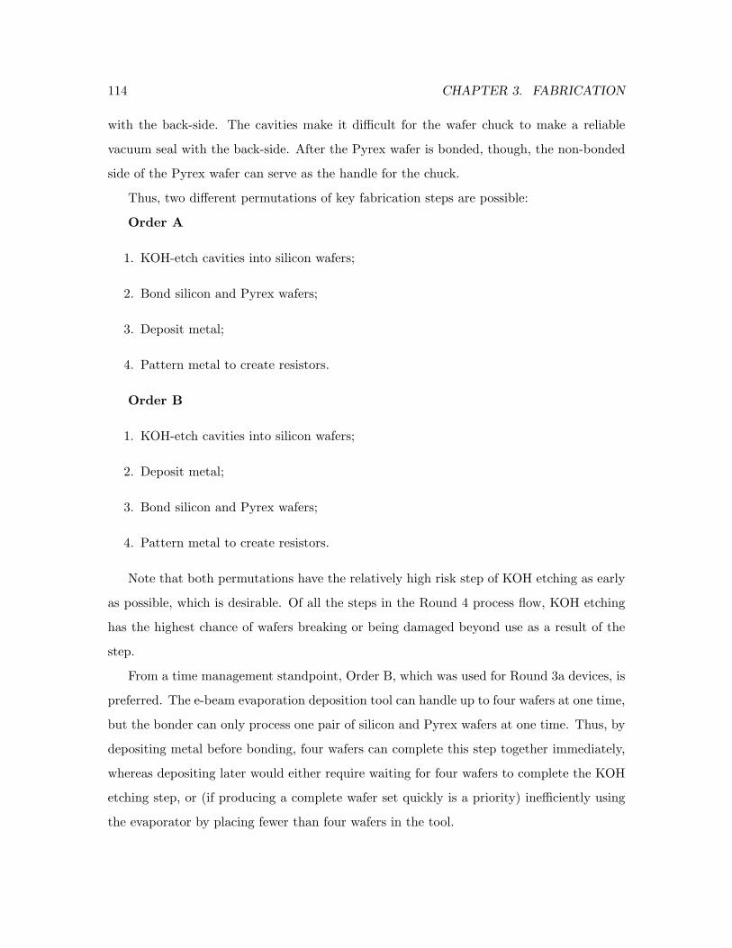
114 CHAPTER 3. FABRICATION
with the back-side. The cavities make it difficult for the wafer chuck to make a reliable
vacuum seal with the back-side. After the Pyrex wafer is bonded, though, the non-bonded
side of the Pyrex wafer can serve as the handle for the chuck.
Thus, two different permutations of key fabrication steps are possible:
Order A
1. KOH-etch cavities into silicon wafers;
2. Bond silicon and Pyrex wafers;
3. Deposit metal;
4. Pattern metal to create resistors.
Order B
1. KOH-etch cavities into silicon wafers;
2. Deposit metal;
3. Bond silicon and Pyrex wafers;
4. Pattern metal to create resistors.
Note that both permutations have the relatively high risk step of KOH etching as early
as possible, which is desirable. Of all the steps in the Round 4 process flow, KOH etching
has the highest chance of wafers breaking or being damaged beyond use as a result of the
step.
From a time management standpoint, Order B, which was used for Round 3a devices, is
preferred. The e-beam evaporation deposition tool can handle up to four wafers at one time,
but the bonder can only process one pair of silicon and Pyrex wafers at one time. Thus, by
depositing metal before bonding, four wafers can complete this step together immediately,
whereas depositing later would either require waiting for four wafers to complete the KOH
etching step, or (if producing a complete wafer set quickly is a priority) inefficiently using
the evaporator by placing fewer than four wafers in the tool.
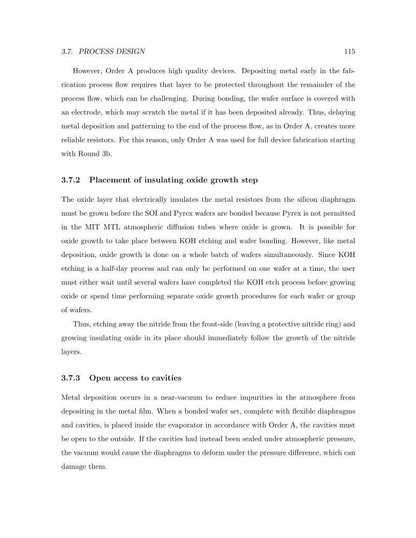
3.7. PROCESS DESIGN 115
However, Order A produces high quality devices. Depositing metal early in the fab-
rication process flow requires that layer to be protected throughout the remainder of the
process flow, which can be challenging. During bonding, the wafer surface is covered with
an electrode, which may scratch the metal if it has been deposited already. Thus, delaying
metal deposition and patterning to the end of the process flow, as in Order A, creates more
reliable resistors. For this reason, only Order A was used for full device fabrication starting
with Round 3b.
3.7.2 Placement of insulating oxide growth step
The oxide layer that electrically insulates the metal resistors from the silicon diaphragm
must be grown before the SOI and Pyrex wafers are bonded because Pyrex is not permitted
in the MIT MTL atmospheric diffusion tubes where oxide is grown. It is possible for
oxide growth to take place between KOH etching and wafer bonding. However, like metal
deposition, oxide growth is done on a whole batch of wafers simultaneously. Since KOH
etching is a half-day process and can only be performed on one wafer at a time, the user
must either wait until several wafers have completed the KOH etch process before growing
oxide or spend time performing separate oxide growth procedures for each wafer or group
of wafers.
Thus, etching away the nitride from the front-side (leaving a protective nitride ring) and
growing insulating oxide in its place should immediately follow the growth of the nitride
layers.
3.7.3 Open access to cavities
Metal deposition occurs in a near-vacuum to reduce impurities in the atmosphere from
depositing in the metal film. When a bonded wafer set, complete with flexible diaphragms
and cavities, is placed inside the evaporator in accordance with Order A, the cavities must
be open to the outside. If the cavities had instead been sealed under atmospheric pressure,
the vacuum would cause the diaphragms to deform under the pressure difference, which can
damage them.
116 CHAPTER 3. FABRICATION
Round 4 devices already have the snaking channel etched in the Pyrex that connects the
cavities with the external environment. The Round 3b devices, however, have each column
of diaphragms sharing an air channel, but the channels are otherwise isolated from the
environment. To open the channels up, one diaphragm in each column is carefully broken
after the wafers are bonded and before the bonded wafer set is placed in the evaporator.
3.7.4 Wet processing bonded wafers
A potential hurdle in assessing the viability of the process flow is how chemicals used
in subsequent wet processing affect the bonded wafer, which has accessible air channels.
The concern is that these chemicals would be stuck inside the air channels. Experiments
demonstrated that wet etchants as varied as piranha, Cr-7 and gold etchant can be removed
by repeatedly rinsing with water, spin drying, and post-baking.
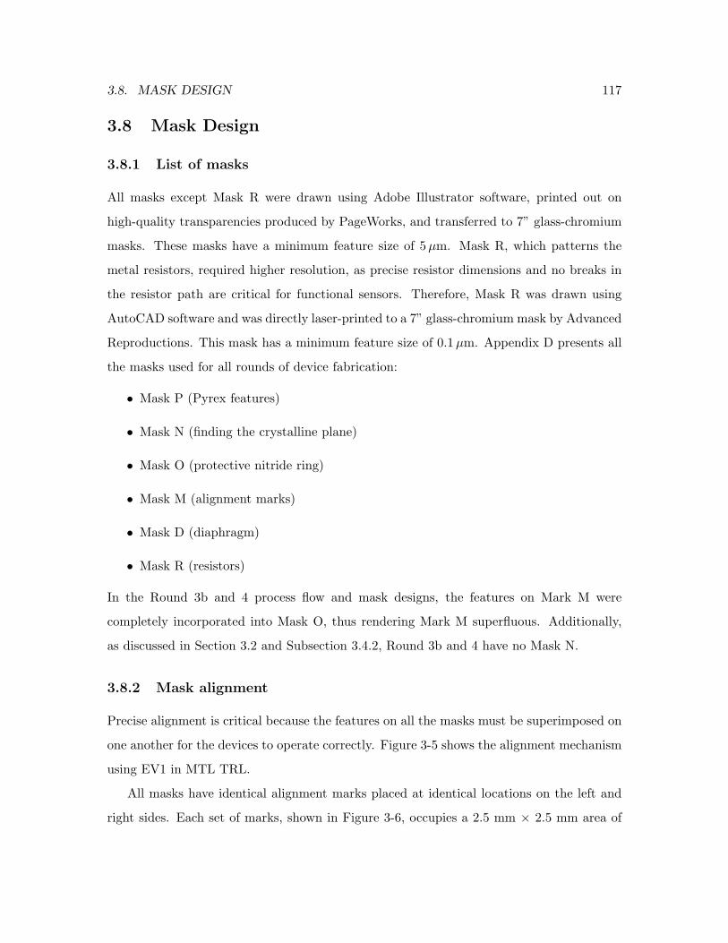
3.8. MASK DESIGN 117
3.8 Mask Design
3.8.1 List of masks
All masks except Mask R were drawn using Adobe Illustrator software, printed out on
high-quality transparencies produced by PageWorks, and transferred to 7” glass-chromium
masks. These masks have a minimum feature size of 5µm. Mask R, which patterns the
metal resistors, required higher resolution, as precise resistor dimensions and no breaks in
the resistor path are critical for functional sensors. Therefore, Mask R was drawn using
AutoCAD software and was directly laser-printed to a 7” glass-chromium mask by Advanced
Reproductions. This mask has a minimum feature size of 0.1µm. Appendix D presents all
the masks used for all rounds of device fabrication:
• Mask P (Pyrex features)
• Mask N (finding the crystalline plane)
• Mask O (protective nitride ring)
• Mask M (alignment marks)
• Mask D (diaphragm)
• Mask R (resistors)
In the Round 3b and 4 process flow and mask designs, the features on Mark M were
completely incorporated into Mask O, thus rendering Mark M superfluous. Additionally,
as discussed in Section 3.2 and Subsection 3.4.2, Round 3b and 4 have no Mask N.
3.8.2 Mask alignment
Precise alignment is critical because the features on all the masks must be superimposed on
one another for the devices to operate correctly. Figure 3-5 shows the alignment mechanism
using EV1 in MTL TRL.
All masks have identical alignment marks placed at identical locations on the left and
right sides. Each set of marks, shown in Figure 3-6, occupies a 2.5 mm × 2.5 mm area of
118 CHAPTER 3. FABRICATION
Figure 3-5: Two-sided alignment mechanism. The diagrams on the left-hand side show theside view of the mask, wafer, chuck and optical system, and the diagrams on the right-handside show the view on the computer monitor. (a) The image of the mask alignment marks isread and projected on the computer monitor. (b) The alignment marks on the bottom-sideof the wafer are also projected on the monitor. (c) The position of the wafer is adjustedby translation and rotation until the two images match acceptably well. Reproduced from[56].

3.8. MASK DESIGN 119
2.5 mm
Figure 3-6: Mask alignment marks.
space. Each set contains four 875 µm × 250 µm rectangles arranged in a cross. In the
center of a cross, there is a much smaller cross made up of four 87.5 µm × 25 µm rectangles.
Two sets of alignment marks, one each from the left and right sides of the mask, are viewed
simultaneously. Once the large crosses on the mask and the wafer are reasonably aligned,
the magnification is increased to image and align the small crosses for fine positional and
angular adjustment.
Each photolithography step requires mask alignment, though for different reasons and
through different mechanisms. The first alignment is Mask P. Since the Pyrex wafer only
has one set of features produced by one mask, and Pyrex etching is identical regardless of
wafer orientation, Mask P only needs to be aligned so that the wafer flats of the Pyrex
wafer and the SOI wafer roughly coincide after bonding, which makes physical handling
easier. As can be seen in Appendix D, some masks have horizontal bars near the bottom
with which the wafer flat can be aligned with the aid of optical instruments.
The second alignment is Mask M (Rounds 1 and 3a) or Mask O (Rounds 3b and 4) for
120 CHAPTER 3. FABRICATION
the SOI wafer. Since this mask forms the reference for all subsequent masks, aligning it
properly is extremely important. As discussed in Subsection 3.4.2, Rounds 1 and 3a have
an additional KOH etch step to find the crystalline plane (after which the alignment marks
in Mask M are laid down), but Rounds 3b and 4 assume the crystalline plane is perfectly
parallel to the wafer flat (and Mask O, which contains the alignment marks from Mask M,
is laid down).
The third alignment is Mask D for the SOI wafer. Since Mask D is applied to the
back-side of the SOI wafer and needs to be aligned to the features from Mask O, which are
on the front-side, a special alignment mechanism is used. Mask D is inserted into EV1 and
adjusted so that the optical sensors are focused on its alignment marks, which are locked
onto the computer monitor. The wafer is placed back-side up into the chuck, and an image
of the front-side wafer marks are superimposed on the computer monitor. The position of
the wafer is then adjusted so that they match.
Finally, the fourth alignment is Mask R for the SOI wafer. This is simply placed so that
its alignment marks are superimposed on those from Mask O.
Chapter 4
Measurements
This chapter discusses the measurements of the fabricated devices. Section 4.1 shows pho-
tographs of the devices. Section 4.2 describes the various instrumentation used to control
applied pressure and make mechanical and electrical measurements. Section 4.3 compares
measurements of the deflection of the center of diaphragm to the model described in Sec-
tion 2.6. Section 4.4 explains how the origin of drifting signals was discovered and managed.
Section 4.5 shows external bridge measurements from isolated sensors. Section 4.6 describes
how underwater testing was done. Finally, Section 4.7 summarizes the results of the mea-
surements.
Note: The pressure indicated by the manometer-controlled experiments is the added
back-side pressure. This is the opposite of the convention discussed in Section 2.6.
121
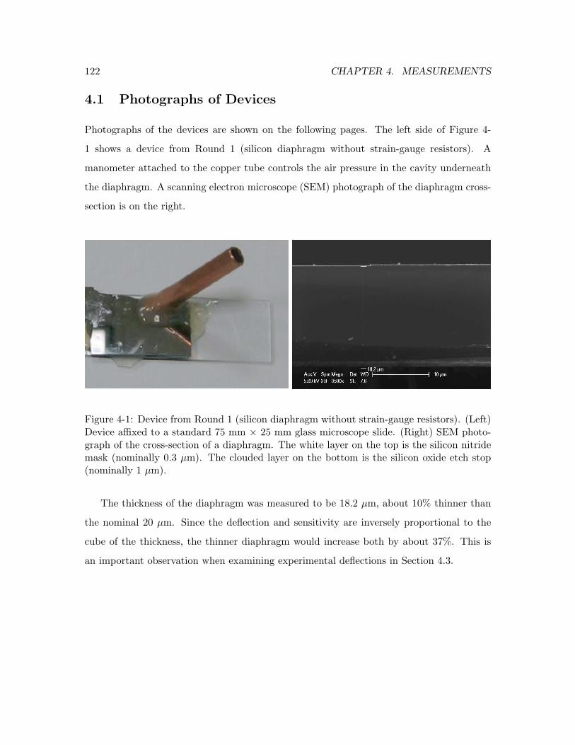
122 CHAPTER 4. MEASUREMENTS
4.1 Photographs of Devices
Photographs of the devices are shown on the following pages. The left side of Figure 4-
1 shows a device from Round 1 (silicon diaphragm without strain-gauge resistors). A
manometer attached to the copper tube controls the air pressure in the cavity underneath
the diaphragm. A scanning electron microscope (SEM) photograph of the diaphragm cross-
section is on the right.
Figure 4-1: Device from Round 1 (silicon diaphragm without strain-gauge resistors). (Left)Device affixed to a standard 75 mm × 25 mm glass microscope slide. (Right) SEM photo-graph of the cross-section of a diaphragm. The white layer on the top is the silicon nitridemask (nominally 0.3 µm). The clouded layer on the bottom is the silicon oxide etch stop(nominally 1 µm).
The thickness of the diaphragm was measured to be 18.2 µm, about 10% thinner than
the nominal 20 µm. Since the deflection and sensitivity are inversely proportional to the
cube of the thickness, the thinner diaphragm would increase both by about 37%. This is
an important observation when examining experimental deflections in Section 4.3.
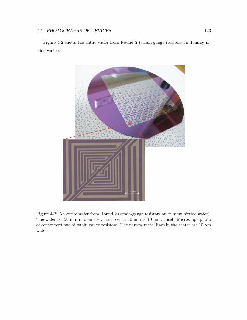
4.1. PHOTOGRAPHS OF DEVICES 123
Figure 4-2 shows the entire wafer from Round 2 (strain-gauge resistors on dummy ni-
tride wafer).
100 um
Figure 4-2: An entire wafer from Round 2 (strain-gauge resistors on dummy nitride wafer).The wafer is 150 mm in diameter. Each cell is 10 mm × 10 mm. Inset: Microscope photoof center portions of strain-gauge resistors. The narrow metal lines in the center are 10 µmwide.
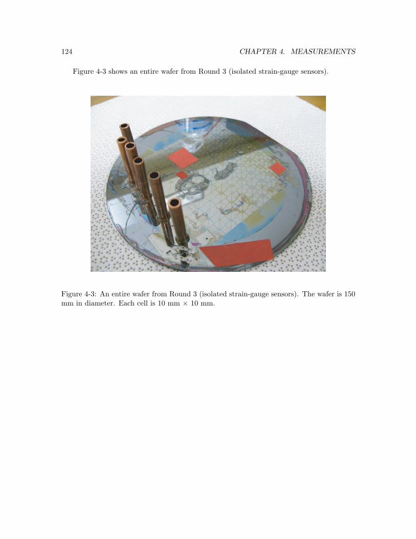
124 CHAPTER 4. MEASUREMENTS
Figure 4-3 shows an entire wafer from Round 3 (isolated strain-gauge sensors).
Figure 4-3: An entire wafer from Round 3 (isolated strain-gauge sensors). The wafer is 150mm in diameter. Each cell is 10 mm × 10 mm.
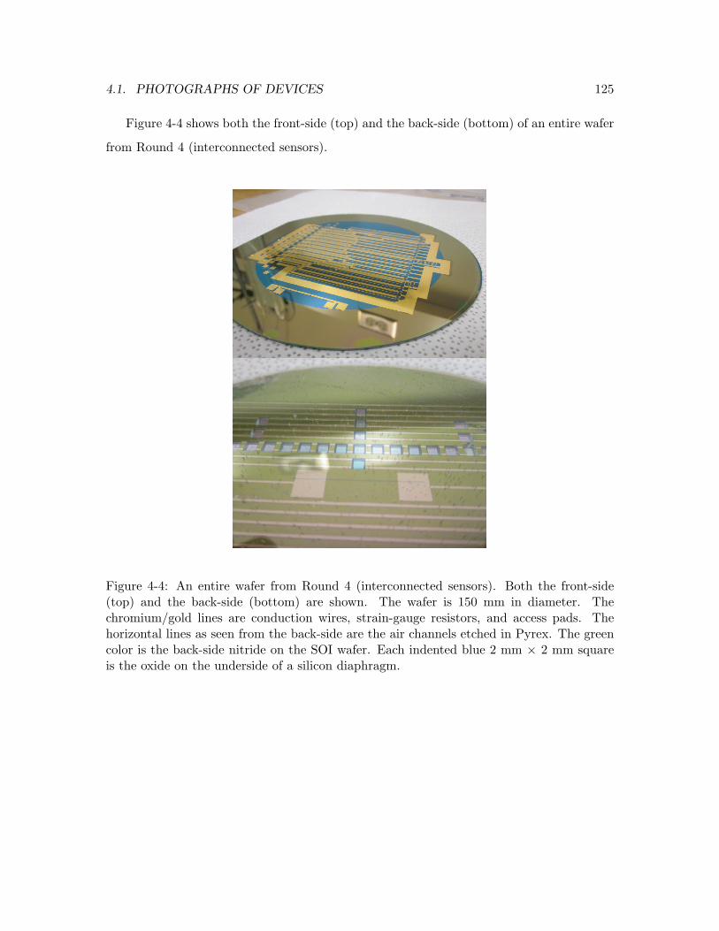
4.1. PHOTOGRAPHS OF DEVICES 125
Figure 4-4 shows both the front-side (top) and the back-side (bottom) of an entire wafer
from Round 4 (interconnected sensors).
Figure 4-4: An entire wafer from Round 4 (interconnected sensors). Both the front-side(top) and the back-side (bottom) are shown. The wafer is 150 mm in diameter. Thechromium/gold lines are conduction wires, strain-gauge resistors, and access pads. Thehorizontal lines as seen from the back-side are the air channels etched in Pyrex. The greencolor is the back-side nitride on the SOI wafer. Each indented blue 2 mm × 2 mm squareis the oxide on the underside of a silicon diaphragm.

126 CHAPTER 4. MEASUREMENTS
4.2 Instrumentation
The various instrumentation used to control applied pressure and make mechanical and
electrical measurements are described below.
4.2.1 Manometer
A manometer was used to control the pressure in the cavities of the devices from Rounds
1 and 3. Figure 4-5 shows a photograph of the manometer. A U-shaped plastic tube is
half-filled with water. One end of the tube is open to the atmosphere. The other end forks
to a syringe and a longer tube that connects to the copper tubes that lead to the sensor
cavities. By moving the piston in the syringe, the air pressure in that portion of the U-tube
changes, which pushes (higher pressure) or pulls (lower pressure) the water. The difference
in the heights of the water between both sides of the U-tube, which is easily seen on the
graph paper behind the tube, corresponds to the pressure difference across the two sides of
the sensor diaphragm. Pressure differences between −1500 Pa and 1500 Pa with a precision
of 10 Pa can be produced.
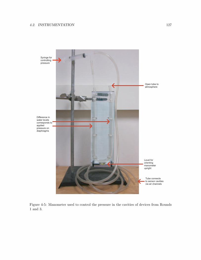
4.2. INSTRUMENTATION 127
Open tube to atmosphere
Tube connects to sensor cavities via air channels
Level for orienting manometer upright
Syringe for controlling pressure
Difference in water levels corresponds to applied pressure on diaphragms
Figure 4-5: Manometer used to control the pressure in the cavities of devices from Rounds1 and 3.
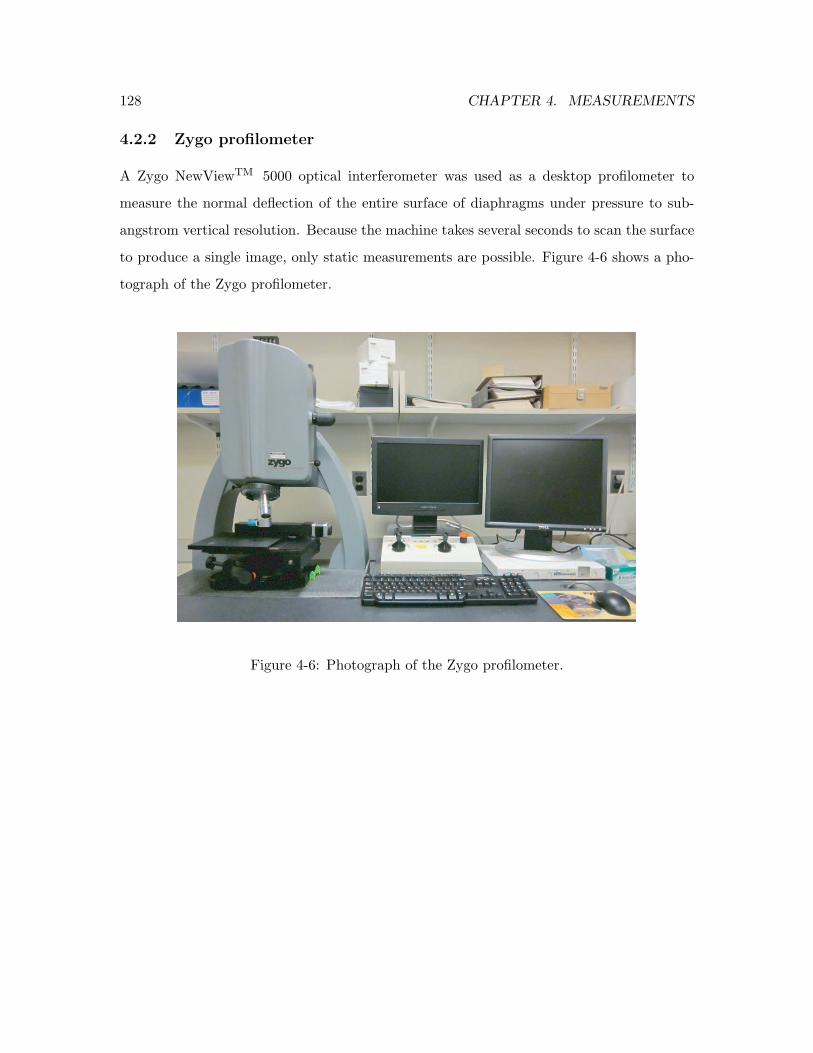
128 CHAPTER 4. MEASUREMENTS
4.2.2 Zygo profilometer
A Zygo NewViewTM 5000 optical interferometer was used as a desktop profilometer to
measure the normal deflection of the entire surface of diaphragms under pressure to sub-
angstrom vertical resolution. Because the machine takes several seconds to scan the surface
to produce a single image, only static measurements are possible. Figure 4-6 shows a pho-
tograph of the Zygo profilometer.
Figure 4-6: Photograph of the Zygo profilometer.
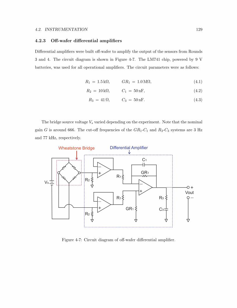
4.2. INSTRUMENTATION 129
4.2.3 Off-wafer differential amplifiers
Differential amplifiers were built off-wafer to amplify the output of the sensors from Rounds
3 and 4. The circuit diagram is shown in Figure 4-7. The LM741 chip, powered by 9 V
batteries, was used for all operational amplifiers. The circuit parameters were as follows:
R1 = 1.5 kΩ, GR1 = 1.0MΩ, (4.1)
R2 = 10 kΩ, C1 = 50nF, (4.2)
R3 = 41Ω, C3 = 50nF. (4.3)
The bridge source voltage Vs varied depending on the experiment. Note that the nominal
gain G is around 666. The cut-off frequencies of the GR1-C1 and R3-C3 systems are 3 Hz
and 77 kHz, respectively.
C1
+
_
GR1
R1
R1
+
+
_
_
Vs
Vout
+
_
Wheatstone Bridge
R2
GR1
R3
C3
R2
Differential Amplifier
Figure 4-7: Circuit diagram of off-wafer differential amplifier.
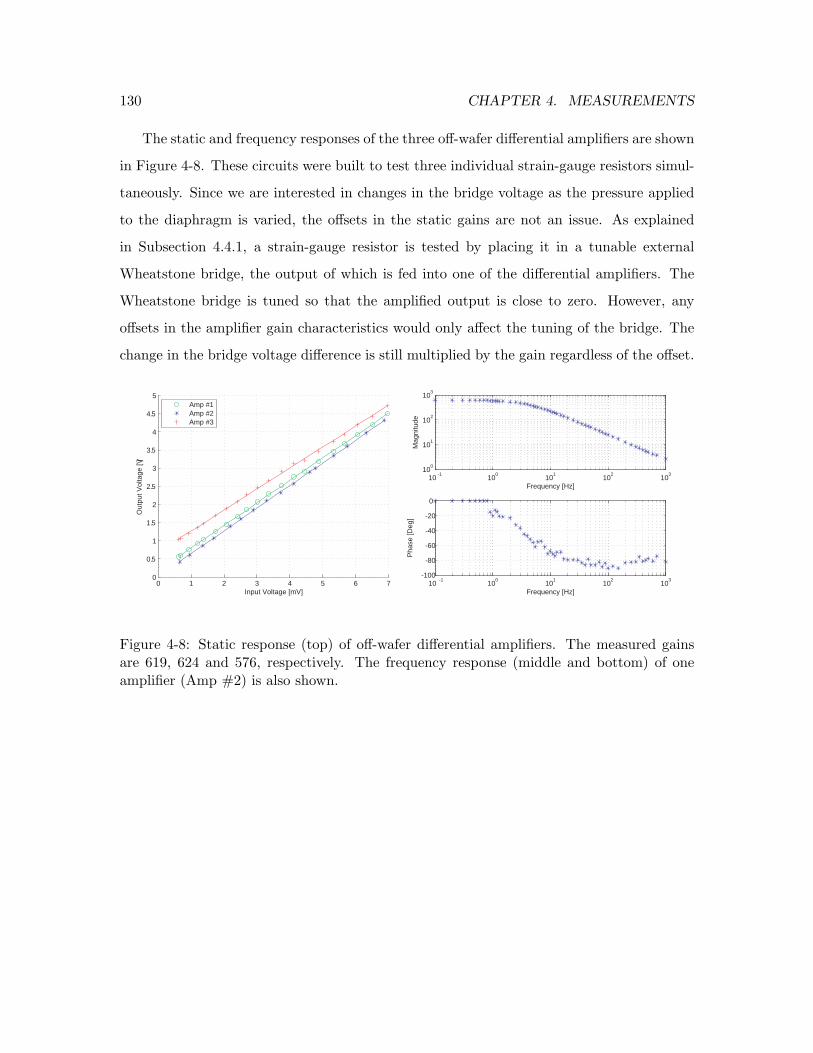
130 CHAPTER 4. MEASUREMENTS
The static and frequency responses of the three off-wafer differential amplifiers are shown
in Figure 4-8. These circuits were built to test three individual strain-gauge resistors simul-
taneously. Since we are interested in changes in the bridge voltage as the pressure applied
to the diaphragm is varied, the offsets in the static gains are not an issue. As explained
in Subsection 4.4.1, a strain-gauge resistor is tested by placing it in a tunable external
Wheatstone bridge, the output of which is fed into one of the differential amplifiers. The
Wheatstone bridge is tuned so that the amplified output is close to zero. However, any
offsets in the amplifier gain characteristics would only affect the tuning of the bridge. The
change in the bridge voltage difference is still multiplied by the gain regardless of the offset.
0 1 2 3 4 5 6 70
0.5
1
1.5
2
2.5
3
3.5
4
4.5
5
Input Voltage [mV]
Out
put V
olta
ge [V
]
Amp #1Amp #2Amp #3
10 -1
100
101
102
103
100
101
102
103
Frequency [Hz]
Mag
nitu
de
10 -1
100
101
102
103
-100
-80
-60
-40
-20
0
Frequency [Hz]
Pha
se [D
eg]
Figure 4-8: Static response (top) of off-wafer differential amplifiers. The measured gainsare 619, 624 and 576, respectively. The frequency response (middle and bottom) of oneamplifier (Amp #2) is also shown.
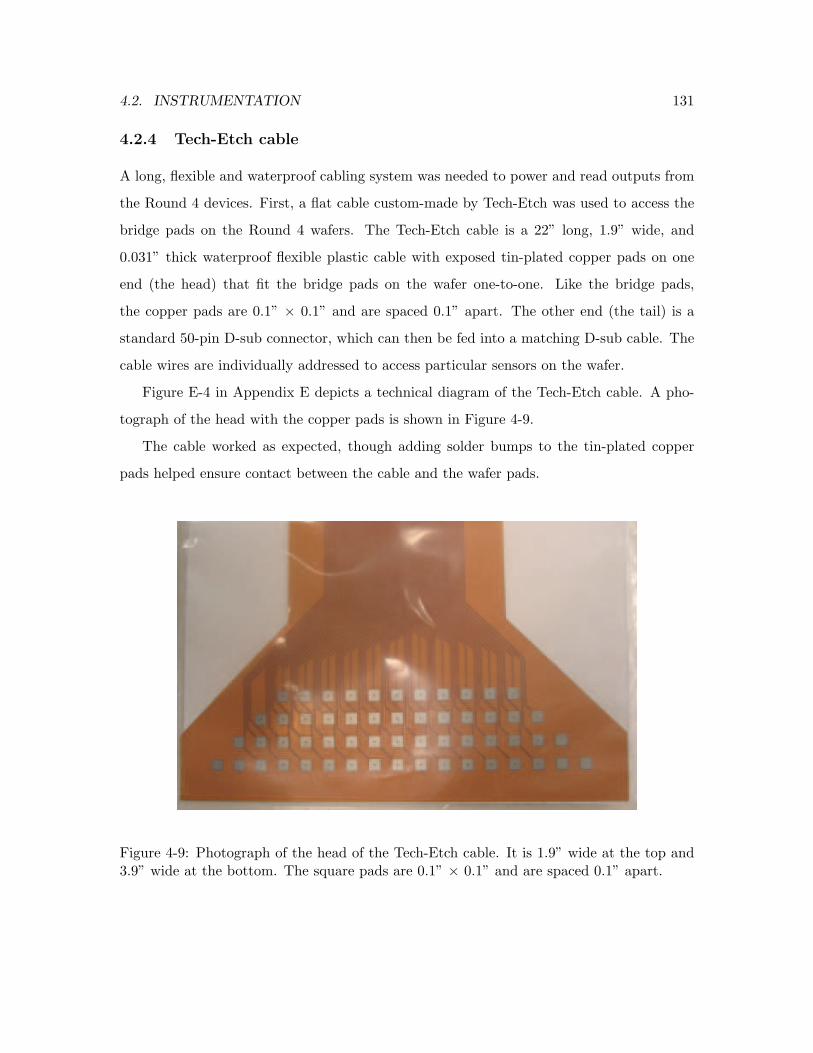
4.2. INSTRUMENTATION 131
4.2.4 Tech-Etch cable
A long, flexible and waterproof cabling system was needed to power and read outputs from
the Round 4 devices. First, a flat cable custom-made by Tech-Etch was used to access the
bridge pads on the Round 4 wafers. The Tech-Etch cable is a 22” long, 1.9” wide, and
0.031” thick waterproof flexible plastic cable with exposed tin-plated copper pads on one
end (the head) that fit the bridge pads on the wafer one-to-one. Like the bridge pads,
the copper pads are 0.1” × 0.1” and are spaced 0.1” apart. The other end (the tail) is a
standard 50-pin D-sub connector, which can then be fed into a matching D-sub cable. The
cable wires are individually addressed to access particular sensors on the wafer.
Figure E-4 in Appendix E depicts a technical diagram of the Tech-Etch cable. A pho-
tograph of the head with the copper pads is shown in Figure 4-9.
The cable worked as expected, though adding solder bumps to the tin-plated copper
pads helped ensure contact between the cable and the wafer pads.
Figure 4-9: Photograph of the head of the Tech-Etch cable. It is 1.9” wide at the top and3.9” wide at the bottom. The square pads are 0.1” × 0.1” and are spaced 0.1” apart.
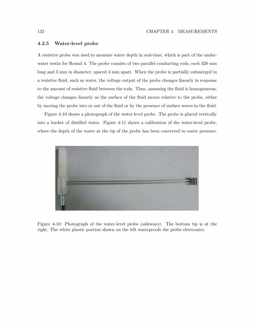
132 CHAPTER 4. MEASUREMENTS
4.2.5 Water-level probe
A resistive probe was used to measure water depth in real-time, which is part of the under-
water testin for Round 4. The probe consists of two parallel conducting rods, each 320 mm
long and 3 mm in diameter, spaced 4 mm apart. When the probe is partially submerged in
a resistive fluid, such as water, the voltage output of the probe changes linearly in response
to the amount of resistive fluid between the rods. Thus, assuming the fluid is homogeneous,
the voltage changes linearly as the surface of the fluid moves relative to the probe, either
by moving the probe into or out of the fluid or by the presence of surface waves in the fluid.
Figure 4-10 shows a photograph of the water-level probe. The probe is placed vertically
into a bucket of distilled water. Figure 4-11 shows a calibration of the water-level probe,
where the depth of the water at the tip of the probe has been converted to water pressure.
Figure 4-10: Photograph of the water-level probe (sideways). The bottom tip is at theright. The white plastic portion shown on the left waterproofs the probe electronics.
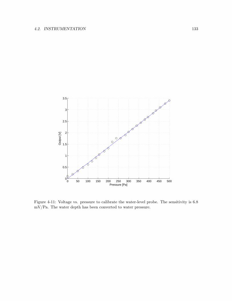
4.2. INSTRUMENTATION 133
0 50 100 150 200 250 300 350 400 450 5000
0.5
1
1.5
2
2.5
3
3.5
Pressure [Pa]
Out
put [
V]
Figure 4-11: Voltage vs. pressure to calibrate the water-level probe. The sensitivity is 6.8mV/Pa. The water depth has been converted to water pressure.
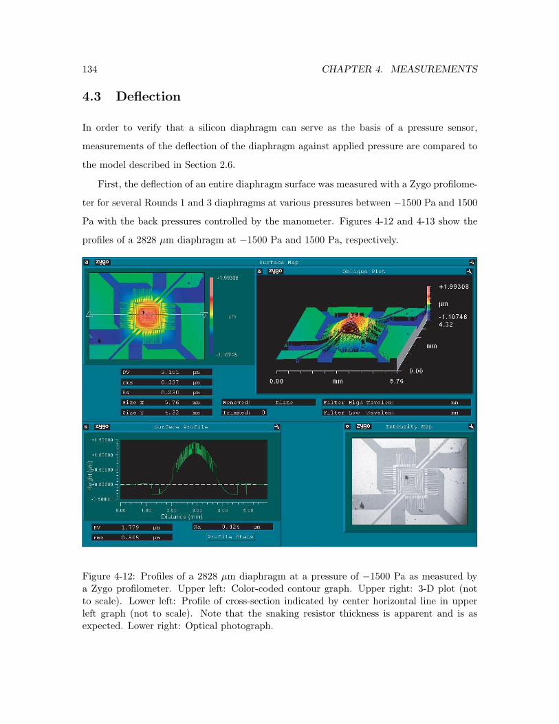
134 CHAPTER 4. MEASUREMENTS
4.3 Deflection
In order to verify that a silicon diaphragm can serve as the basis of a pressure sensor,
measurements of the deflection of the diaphragm against applied pressure are compared to
the model described in Section 2.6.
First, the deflection of an entire diaphragm surface was measured with a Zygo profilome-
ter for several Rounds 1 and 3 diaphragms at various pressures between −1500 Pa and 1500
Pa with the back pressures controlled by the manometer. Figures 4-12 and 4-13 show the
profiles of a 2828 µm diaphragm at −1500 Pa and 1500 Pa, respectively.
Figure 4-12: Profiles of a 2828 µm diaphragm at a pressure of −1500 Pa as measured bya Zygo profilometer. Upper left: Color-coded contour graph. Upper right: 3-D plot (notto scale). Lower left: Profile of cross-section indicated by center horizontal line in upperleft graph (not to scale). Note that the snaking resistor thickness is apparent and is asexpected. Lower right: Optical photograph.
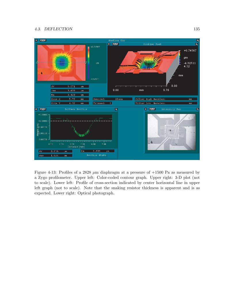
4.3. DEFLECTION 135
Figure 4-13: Profiles of a 2828 µm diaphragm at a pressure of +1500 Pa as measured bya Zygo profilometer. Upper left: Color-coded contour graph. Upper right: 3-D plot (notto scale). Lower left: Profile of cross-section indicated by center horizontal line in upperleft graph (not to scale). Note that the snaking resistor thickness is apparent and is asexpected. Lower right: Optical photograph.
136 CHAPTER 4. MEASUREMENTS
Then, detailed measurements of the deflection at the center of the diaphragm (c1) at
various pressures (P ) between −1500 Pa and 1500 Pa for diaphragms of three different sizes
were made. Figure 4-14 shows the results from two diaphragms of sizes 2000 µm and 2828
µm. Figure 4-15 shows the results from a 4000 µm diaphragm. The slopes of the best-fit
lines for the experimental data are given in Table 4.1, along with the theoretical relationship
between c1 and P for various diaphragm lengths L (all with thicknessH = 20µm) calculated
in Section 2.10.
DiaphragmLength (µm)
Theoreticalc1/P (nm/Pa)
Experimentalc1/P (nm/Pa)
1000 0.0118 —
1414 0.0470 —
2000 0.188 0.381
2828 0.752 1.34
4000 3.01 8.97
Table 4.1: Slopes c1/P for various diaphragm lengths L.
The difference between theory and experiment could be the result of several phe-
nomenon. For example, the silicon oxide grown and metal deposited on the diaphragm
occurred under high temperature and low pressure, respectively. These processes could
have pre-stressed the diaphragm layers to alter the deflection-pressure characteristics. Re-
call from Subsection 2.6.4 that the complete relationship between pressure (P ) and center
deflection (c1) is
P =
Cr
[
σ0H
L2
]
+ Cb
[
EH3
(1− ν2)L4
]
c1 + Csfs(ν)
[
EH
(1− ν)L4
]
c31, (4.4)
where Cr, Cb and Cs are constants, which refer to the residual stress, bending, and stretch-
ing terms, respectively; σ0 is residual stress in the diaphragm; and fs(ν) is a function of ν.
Since c1 ≪ H, the linear c1 terms dominate over the cubic c31 term. Thus, we obtain
P ≈
Cr
[
σ0H
L2
]
+ Cb
[
EH3
(1− ν2)L4
]
c1. (4.5)
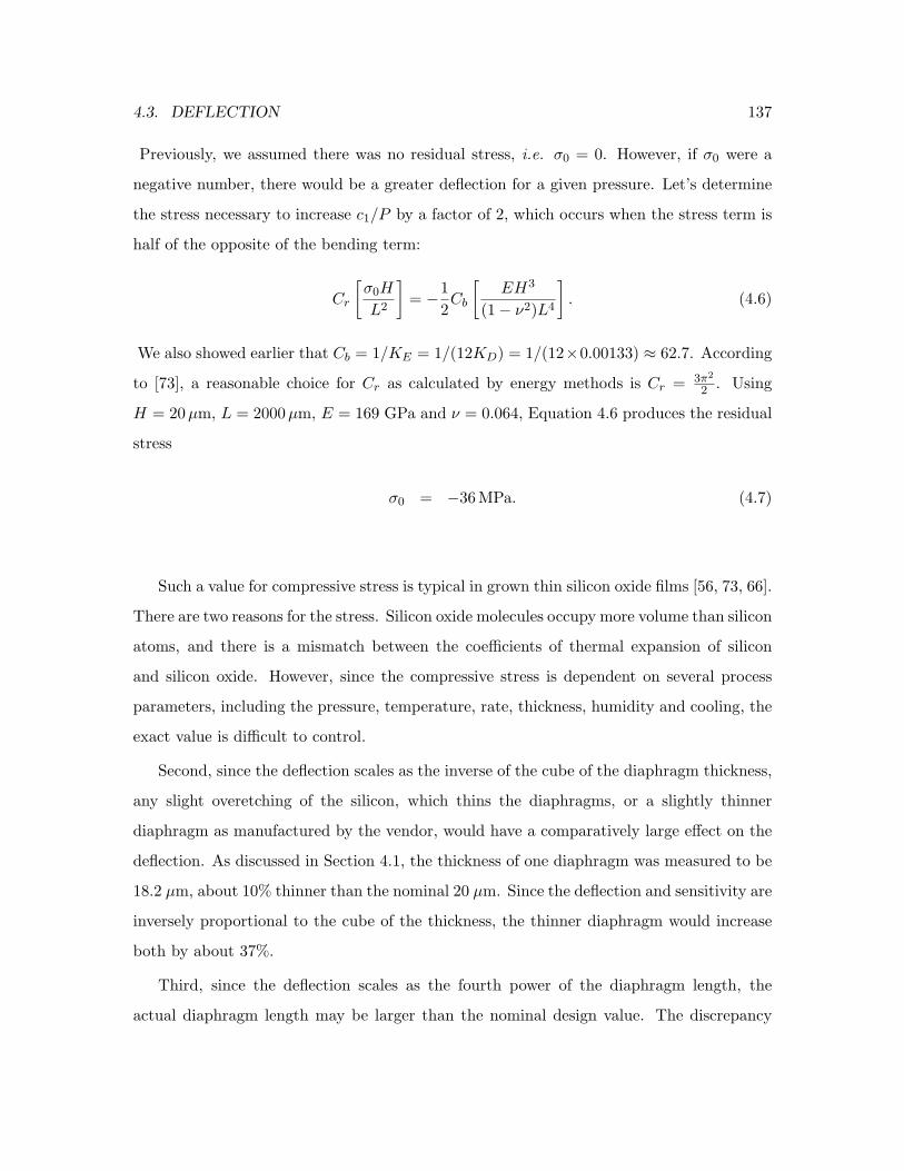
4.3. DEFLECTION 137
Previously, we assumed there was no residual stress, i.e. σ0 = 0. However, if σ0 were a
negative number, there would be a greater deflection for a given pressure. Let’s determine
the stress necessary to increase c1/P by a factor of 2, which occurs when the stress term is
half of the opposite of the bending term:
Cr
[
σ0H
L2
]
= −1
2Cb
[
EH3
(1− ν2)L4
]
. (4.6)
We also showed earlier that Cb = 1/KE = 1/(12KD) = 1/(12×0.00133) ≈ 62.7. According
to [73], a reasonable choice for Cr as calculated by energy methods is Cr = 3π2
2 . Using
H = 20µm, L = 2000µm, E = 169 GPa and ν = 0.064, Equation 4.6 produces the residual
stress
σ0 = −36MPa. (4.7)
Such a value for compressive stress is typical in grown thin silicon oxide films [56, 73, 66].
There are two reasons for the stress. Silicon oxide molecules occupy more volume than silicon
atoms, and there is a mismatch between the coefficients of thermal expansion of silicon
and silicon oxide. However, since the compressive stress is dependent on several process
parameters, including the pressure, temperature, rate, thickness, humidity and cooling, the
exact value is difficult to control.
Second, since the deflection scales as the inverse of the cube of the diaphragm thickness,
any slight overetching of the silicon, which thins the diaphragms, or a slightly thinner
diaphragm as manufactured by the vendor, would have a comparatively large effect on the
deflection. As discussed in Section 4.1, the thickness of one diaphragm was measured to be
18.2 µm, about 10% thinner than the nominal 20 µm. Since the deflection and sensitivity are
inversely proportional to the cube of the thickness, the thinner diaphragm would increase
both by about 37%.
Third, since the deflection scales as the fourth power of the diaphragm length, the
actual diaphragm length may be larger than the nominal design value. The discrepancy
138 CHAPTER 4. MEASUREMENTS
has several sources. As discussed in Section 3.4.2, devices from Rounds 3b and 4 assumed
that the wafer flat was parallel to a 〈110〉 direction. If this is tilted by an angle, the
KOH etch would expand the diaphragm to be bounded by the smallest 〈110〉-bounded
rectangle that contains the designed square. A one degree tilt would increase the length by
about 1.7 %. Next, as discussed in Section 2.6, we assumed the diaphragm is fixed to the
cavity edges as an ideal boundary condition. However, in reality, part of the surface of the
silicon immediately outside the diaphragm would be deflected as well, which increases the
effective diaphragm length. The correction to the effective length is on the order of several
thicknesses of the diaphragm. Since the L/H = 100 for the L = 2000µm diaphragms, this
could contribute a few percent to the additional flexibility of the diaphragm. Finally, as
discussed in Section 3.4, the walls of the KOH cavities produced form 54.7 angles with
the surface plane. Thus, the nitride mask windows need to be larger than the designed
diaphragm size where each window side is moved outwards by x = T cot 54.7, where T is
the handle wafer thickness. This was taken into account when the back-side mask for the
diaphragm windows, Mask D, was created. However, if the actual value of T is smaller than
the nominal value, which was used in mask design, then the diaphragms will be larger than
intended. For every 15 µm the actual handle wafer thickness is smaller than the nominal
value, the length of the diaphragm increases by 1%.
All of the phenomena discussed above contribute to greater deflection for a given applied
pressure. In any case, the diaphragms are more sensitive than they were designed to be.
Furthermore, they display consistent results over long periods of time and have no hysteretic
effects, which means they can be reliably calibrated as pressure sensors.
Note that the 4000 µm diaphragm is flexible enough that the center deflection is no
longer linear with pressure in the −1500 to 1500 Pa range. As discussed earlier in Subsec-
tion 2.6.4 and Section 2.10, linearity is only assumed when the deflection of that diaphragm
is less than 10% of the diaphragm thickness, which for the 4000 µm diaphragm, restricts
absolute pressure differences to less than 664 Pa. Regardless, nonlinearity is an acceptable
characteristic for a pressure sensor. Like the smaller diaphragms, the nonlinearity of the
large diaphragm is consistent over time and thus can be calibrated.
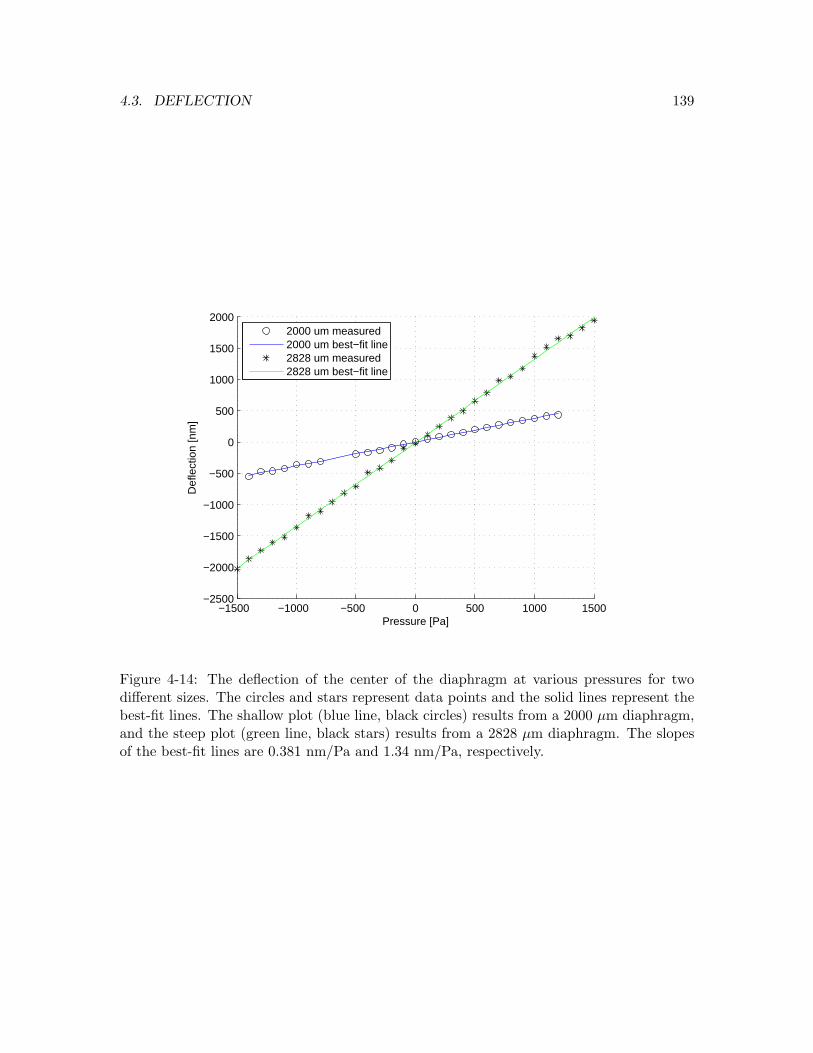
4.3. DEFLECTION 139
−1500 −1000 −500 0 500 1000 1500−2500
−2000
−1500
−1000
−500
0
500
1000
1500
2000
Pressure [Pa]
Def
lect
ion
[nm
]
2000 um measured2000 um best−fit line2828 um measured2828 um best−fit line
Figure 4-14: The deflection of the center of the diaphragm at various pressures for twodifferent sizes. The circles and stars represent data points and the solid lines represent thebest-fit lines. The shallow plot (blue line, black circles) results from a 2000 µm diaphragm,and the steep plot (green line, black stars) results from a 2828 µm diaphragm. The slopesof the best-fit lines are 0.381 nm/Pa and 1.34 nm/Pa, respectively.
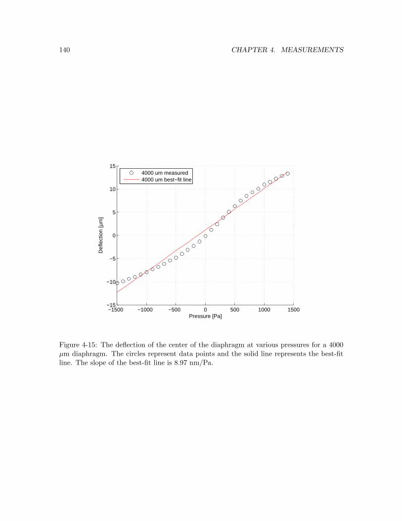
140 CHAPTER 4. MEASUREMENTS
−1500 −1000 −500 0 500 1000 1500−15
−10
−5
0
5
10
15
Pressure [Pa]
Def
lect
ion
[µm
]
4000 um measured4000 um best−fit line
Figure 4-15: The deflection of the center of the diaphragm at various pressures for a 4000µm diaphragm. The circles represent data points and the solid line represents the best-fitline. The slope of the best-fit line is 8.97 nm/Pa.
4.4. DRIFTING SIGNALS 141
4.4 Drifting Signals
After the diaphragms were confirmed to mechanically deflect in response to pressure, elec-
trical measurements of the sensors were made. The resistances of the strain-gauge resistors
across a Round 3 wafer ranged from 15 kΩ to 18 kΩ. The monotonic gradient in resistance
change as one sweeps across the wafer is likely due to a gradient in metal thickness dur-
ing e-beam deposition, which is typical. Then, the output of Wheatstone bridges made of
external resistors and individual strain-gauge resistors were tested as applied pressure was
varied. However, contact resistance between the chromium resistor pads and microscope
probes was found to be unstable, and steps were taken to stabilize it. This experience led
to the addition of gold on the chromium pads for the fabrication of Round 4 devices. This
series of experiments is discussed in below.
4.4.1 Experimental set up
A pair of microscope probes were pressed on the pads of a strain-gauge resistor to enable
connection to an external, well-characterized circuit. A Wheatstone bridge was set up off-
wafer using two fixed resistors, one variable resistor in the form of two potentiometers in
series, and one device strain-gauge resistor. The fixed resistors were selected to approxi-
mately match the expected resistance of the strain gauge. The output of the quarter bridge
is then fed into the differential amplifier described in Subsection 4.2.3. Two potentiometers,
one much larger than the other, were used in series to allow for coarse and fine tuning. The
potentiometers are adjusted until the bridge measures close to zero output for zero input,
which is a highly delicate procedure. This experimental set up is depicted in Figure 4-16.
The amplified output of an external bridge testing a single resistor on a 4000 µm di-
aphragm at zero applied pressure was measured over an 80-second period. Figure 4-17
shows shows raw (blue) and time-averaged (green) traces. The signal slowly drifts over the
course of the 80-second period. This effect was consistently observed for all resistors tested.
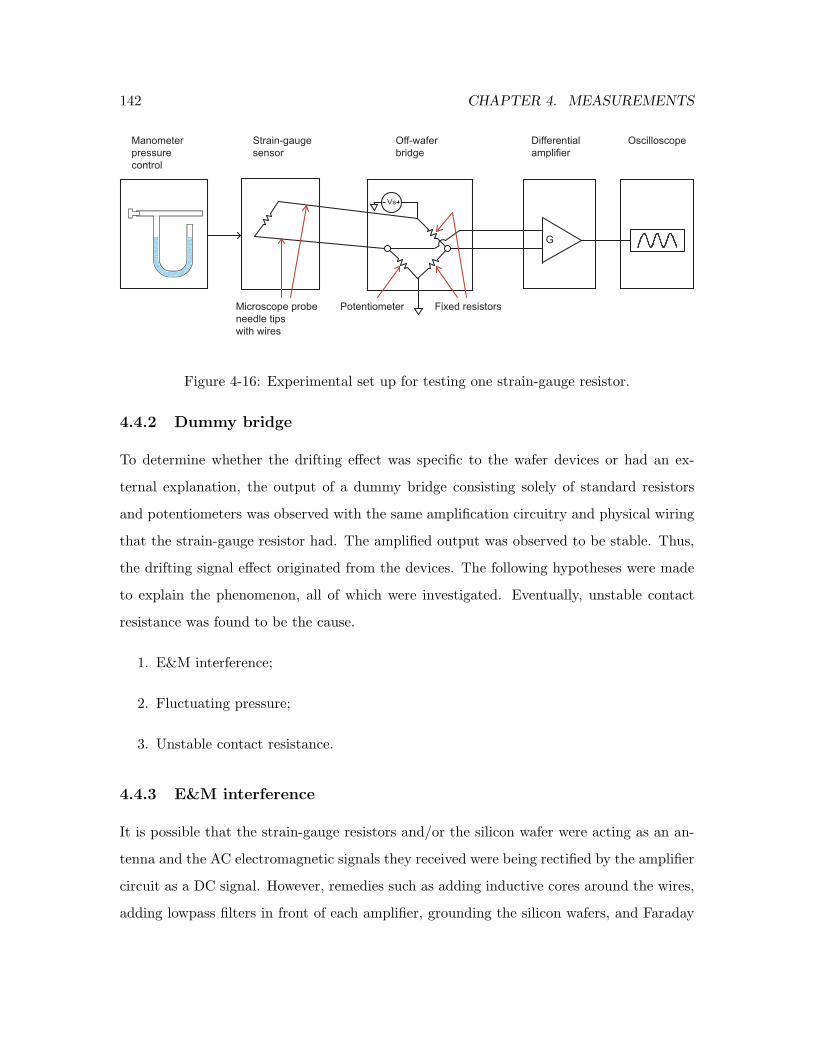
142 CHAPTER 4. MEASUREMENTS
Vs
Differential
amplifier
Oscilloscope
G
Fixed resistors
Manometer
pressure
control
Microscope probe
needle tips
with wires
Potentiometer
Strain-gauge
sensor
Off-wafer
bridge
Figure 4-16: Experimental set up for testing one strain-gauge resistor.
4.4.2 Dummy bridge
To determine whether the drifting effect was specific to the wafer devices or had an ex-
ternal explanation, the output of a dummy bridge consisting solely of standard resistors
and potentiometers was observed with the same amplification circuitry and physical wiring
that the strain-gauge resistor had. The amplified output was observed to be stable. Thus,
the drifting signal effect originated from the devices. The following hypotheses were made
to explain the phenomenon, all of which were investigated. Eventually, unstable contact
resistance was found to be the cause.
1. E&M interference;
2. Fluctuating pressure;
3. Unstable contact resistance.
4.4.3 E&M interference
It is possible that the strain-gauge resistors and/or the silicon wafer were acting as an an-
tenna and the AC electromagnetic signals they received were being rectified by the amplifier
circuit as a DC signal. However, remedies such as adding inductive cores around the wires,
adding lowpass filters in front of each amplifier, grounding the silicon wafers, and Faraday
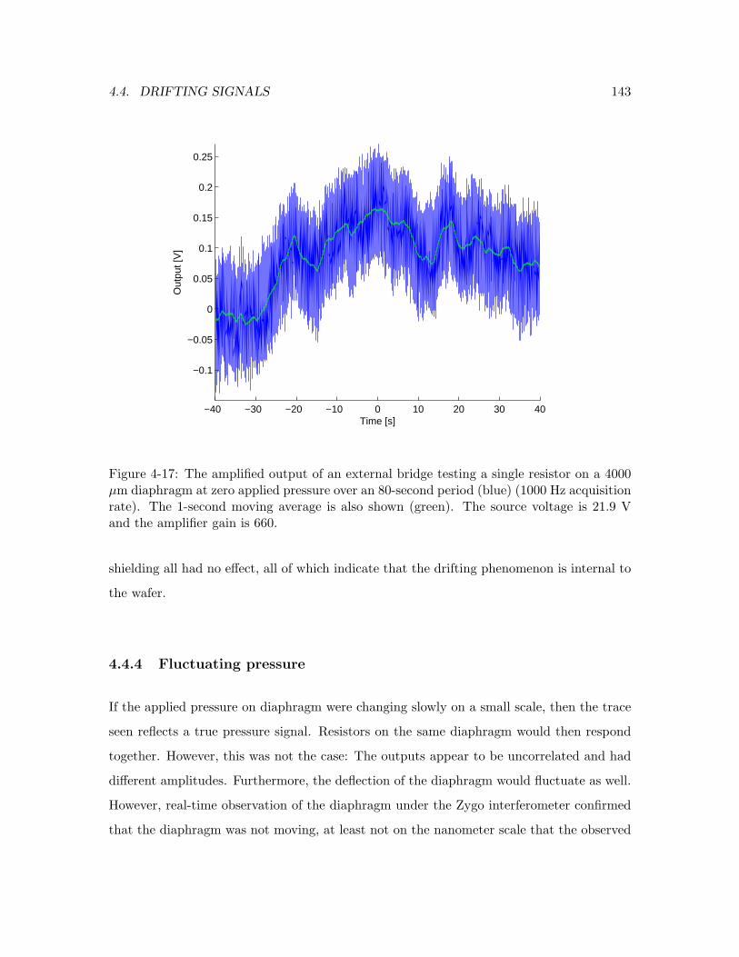
4.4. DRIFTING SIGNALS 143
−40 −30 −20 −10 0 10 20 30 40
−0.1
−0.05
0
0.05
0.1
0.15
0.2
0.25
Time [s]
Out
put [
V]
Figure 4-17: The amplified output of an external bridge testing a single resistor on a 4000µm diaphragm at zero applied pressure over an 80-second period (blue) (1000 Hz acquisitionrate). The 1-second moving average is also shown (green). The source voltage is 21.9 Vand the amplifier gain is 660.
shielding all had no effect, all of which indicate that the drifting phenomenon is internal to
the wafer.
4.4.4 Fluctuating pressure
If the applied pressure on diaphragm were changing slowly on a small scale, then the trace
seen reflects a true pressure signal. Resistors on the same diaphragm would then respond
together. However, this was not the case: The outputs appear to be uncorrelated and had
different amplitudes. Furthermore, the deflection of the diaphragm would fluctuate as well.
However, real-time observation of the diaphragm under the Zygo interferometer confirmed
that the diaphragm was not moving, at least not on the nanometer scale that the observed
144 CHAPTER 4. MEASUREMENTS
change would require.1
4.4.5 Unstable contact resistance
The strain-gauge resistors are being accessed by microscope probe needles pressed into the
resistor pads. The pads consist of thin (2000 A) film chromium, plus some native chromium
oxide on the exposed surface. To access the chromium, the probe needle is carefully but
firmly scratched into the film by precision-tuning the probe arm. If the contact resistance
between the probe needles and the chromium pads fluctuates, the output of the bridge
would fluctuate.
To test this hypothesis, a dummy bridge consisting solely of standard resistors and
potentiometers, like the one earlier, was set up. However, the path between two dummy
resistors was routed to two microscope probes pressed against the same chromium pad.
A drifting signal similar to the trace in Figure 4-17 appeared. Since the only difference
between this arrangement and the dummy bridge described in 4.4.2 is the path through
the chromium pad, the experiments prove that a fluctuating contact resistance between the
microscope probe needles and chromium pads is the source of the drifting bridge signal.
4.4.6 Stabilizing the contact resistance
Several approaches were pursued to stabilize the fluctuating contact resistance. Because
the resistor pads are coated with a thin chromium oxide, all required scratching or wet
etching with KOH to remove a portion of it. First, wire-bonding 50-µm gold wires onto the
pads was attempted. Since gold does not adhere to the pads directly due to the presence
of chromium oxide, a conducting epoxy is necessary, even after scratching away the oxide.
This method successfully accessed the chromium pads, but the gold wires were extremely
delicate and the procedure is difficult to replicate reliably for several pads without the wires
eventually falling off from the weak connections. Next, copper magnet wire, which is thicker
and stronger than the gold wires, was attempted. Because of its weight, a combination of
1Although it takes several seconds for the Zygo to take a complete profile measurement, the microscope onthe Zygo allows the user to see optical interference patterns on a surface in real time. Any nanometer-scalechanges would be immediately observed.
4.4. DRIFTING SIGNALS 145
CircuitWorks R© conductive silver epoxy (to affix wires to the Cr pads) and LOCTITE R©
Fixmaster fast cure epoxy (to provide mechanical support) was required to achieve a stable
connection to the resistors. Like the gold wires, a successful electrical connection is made,
but the wires eventually lose contact with the pads.
Finally, the microscope probe needles were permanently affixed into the pads with both
conducting and mechanical epoxy. The process is as follows:
1. Clip two 3 mm tips from the microscope probe needles.
2. Use precision probe holders to place the tips on the two chromium pads of one strain-
gauge resistor.
3. Apply KOH as a wet etch to dissolve the thin chromium oxide film.
4. Add conducting epoxy around the contact point.
5. Wait at least 4 hours for the conducting epoxy to harden.
6. Add mechanical epoxy around the entire pair of pads.
7. Wait at least 12 hours for the mechanical epoxy to harden.
8. Carefully unscrew the tips from the probe holders.
9. Solder the wires to the tips.
10. Add waterproofing (either Parylene or rubber cement).
During epoxy hardening, probe tips must be held in place, but the support must be able to
be removed without releasing stress. A photograph of the result is shown in Figure 4-18.
Unfortunately, the tips eventually lost contact with the pads. It is believed that the
regular epoxy does not grip the metal probe needle tips tightly enough. Thus, another
mechanical epoxy, WEST SYSTEM R©, was tested.2 This was found to work best; the
2The specific WEST SYSTEM R© epoxy used is a marine-grade epoxy consisting of three components:(1) the 105 Epoxy Resin R©, a low-viscosity liquid epoxy resin that does not shrink after curing; (2) the 205Fast Hardener R©, a medium-viscosity epoxy curing agent; and (3) the 403 Microfibers R©, a fine fiber blendused as a thickening additive.
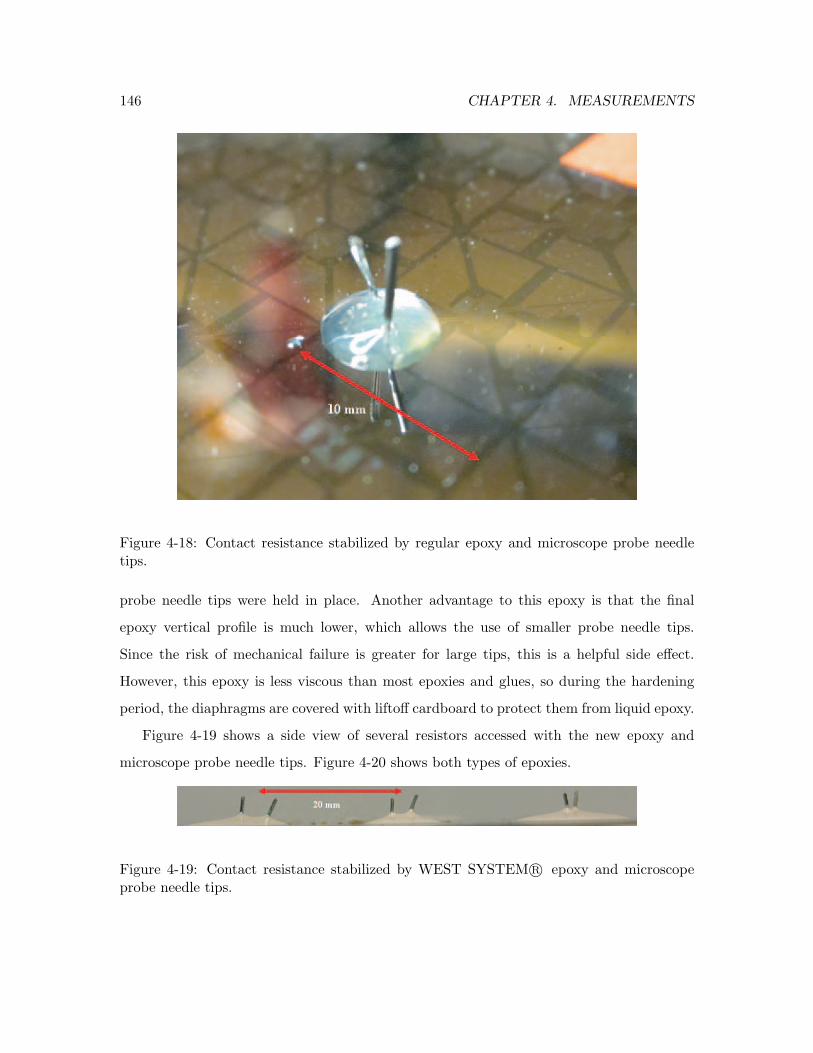
146 CHAPTER 4. MEASUREMENTS
Figure 4-18: Contact resistance stabilized by regular epoxy and microscope probe needletips.
probe needle tips were held in place. Another advantage to this epoxy is that the final
epoxy vertical profile is much lower, which allows the use of smaller probe needle tips.
Since the risk of mechanical failure is greater for large tips, this is a helpful side effect.
However, this epoxy is less viscous than most epoxies and glues, so during the hardening
period, the diaphragms are covered with liftoff cardboard to protect them from liquid epoxy.
Figure 4-19 shows a side view of several resistors accessed with the new epoxy and
microscope probe needle tips. Figure 4-20 shows both types of epoxies.
Figure 4-19: Contact resistance stabilized by WEST SYSTEM R© epoxy and microscopeprobe needle tips.
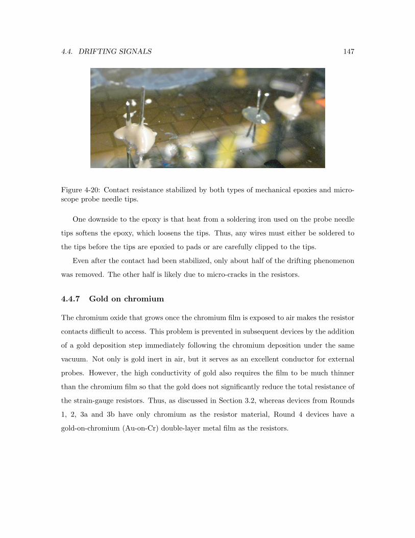
4.4. DRIFTING SIGNALS 147
Figure 4-20: Contact resistance stabilized by both types of mechanical epoxies and micro-scope probe needle tips.
One downside to the epoxy is that heat from a soldering iron used on the probe needle
tips softens the epoxy, which loosens the tips. Thus, any wires must either be soldered to
the tips before the tips are epoxied to pads or are carefully clipped to the tips.
Even after the contact had been stabilized, only about half of the drifting phenomenon
was removed. The other half is likely due to micro-cracks in the resistors.
4.4.7 Gold on chromium
The chromium oxide that grows once the chromium film is exposed to air makes the resistor
contacts difficult to access. This problem is prevented in subsequent devices by the addition
of a gold deposition step immediately following the chromium deposition under the same
vacuum. Not only is gold inert in air, but it serves as an excellent conductor for external
probes. However, the high conductivity of gold also requires the film to be much thinner
than the chromium film so that the gold does not significantly reduce the total resistance of
the strain-gauge resistors. Thus, as discussed in Section 3.2, whereas devices from Rounds
1, 2, 3a and 3b have only chromium as the resistor material, Round 4 devices have a
gold-on-chromium (Au-on-Cr) double-layer metal film as the resistors.
148 CHAPTER 4. MEASUREMENTS
4.5 External Bridge Measurements from Isolated Sensors
After the contact resistance between the microscope probe needle tips and the strain-gauge
resistor pads had been stabilized, the isolated strain-gauge resistors of the Round 3b devices
are tested. Like the experimental set up described in Subsection 4.4.1, the strain-gauge
resistors are individually tested by placing each in an external Wheatstone bridge, where
the other three Wheatstone components are fixed resistors and potentiometers. The bridge
output is amplified by the differential amplifier described in Subsection 4.2.3. As before, the
potentiometers were fine-tuned to set the output voltage to be as close to zero as possible
when no pressure is applied to the diaphragms.
The manometer described in Subsection 4.2.1 is attached to the copper tubes on the
wafer, which enables the experimenter to control the back pressure on a column of sen-
sors. Since the manometer is water-based, the range and resolution of differential pressure
between atmospheric pressure on the top of the diaphragms and the back pressure on the
bottom is determined by the size of the manometer. We can produce pressure differences
between −1500 Pa and 1500 Pa with a precision of 10 Pa.
Figure 4-21 shows the output of an external bridge from a 4000 µm diaphragm un-
dergoing ±1600 Pa changes. The source voltage is 21.9 V and the amplifier gain is 660.
Figure 4-22 shows the output from the same system, but with ±200 Pa changes. Finally,
Figure 4-23 shows the output from a single 200 Pa step. Note that the slow time response,
as evidenced by a first-order time constant of around 1 s, is due to the pressure tubes and
the amplifier circuits, not the sensors themselves. As expected, the outputs respond to
pressure change.
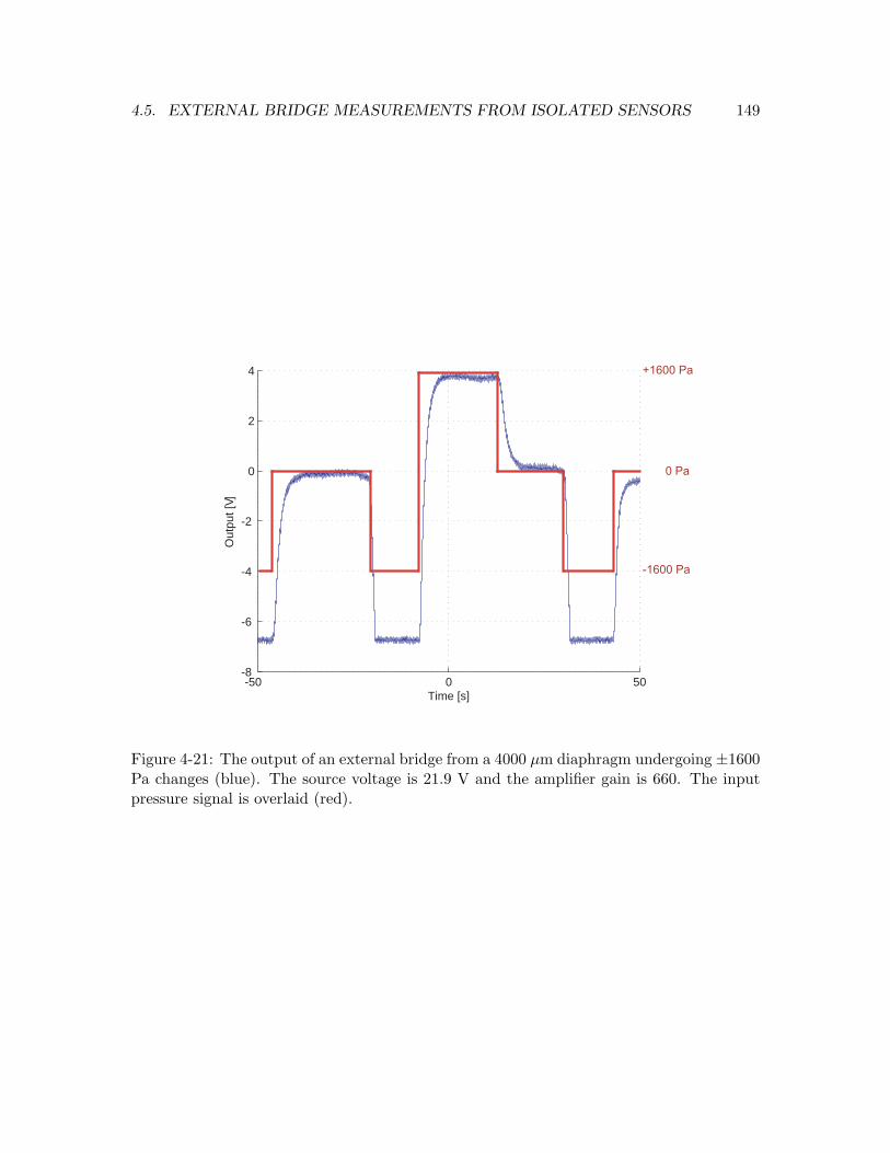
4.5. EXTERNAL BRIDGE MEASUREMENTS FROM ISOLATED SENSORS 149
-50 0 50-8
-6
-4
-2
0
2
4
Time [s]
Out
put [
V]
-1600 Pa
0 Pa
+1600 Pa
Figure 4-21: The output of an external bridge from a 4000 µm diaphragm undergoing ±1600Pa changes (blue). The source voltage is 21.9 V and the amplifier gain is 660. The inputpressure signal is overlaid (red).
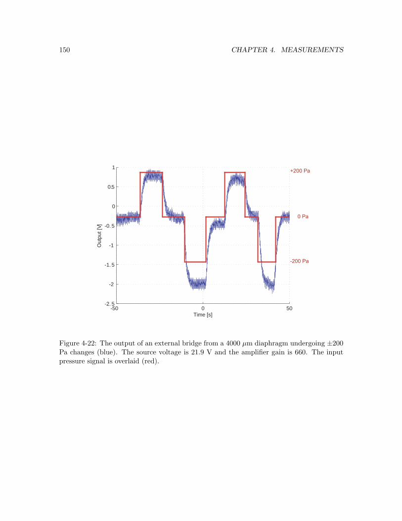
150 CHAPTER 4. MEASUREMENTS
-50 0 50-2. 5
-2
-1. 5
-1
-0. 5
0
0.5
1
Time [s]
Out
put [
V]
-200 Pa
0 Pa
+200 Pa
Figure 4-22: The output of an external bridge from a 4000 µm diaphragm undergoing ±200Pa changes (blue). The source voltage is 21.9 V and the amplifier gain is 660. The inputpressure signal is overlaid (red).
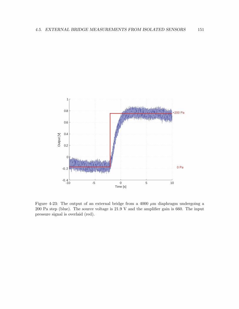
4.5. EXTERNAL BRIDGE MEASUREMENTS FROM ISOLATED SENSORS 151
-10 -5 0 5 10-0. 4
-0. 2
0
0.2
0.4
0.6
0.8
1
Time [s]
Out
put [
V]
+200 Pa
0 Pa
Figure 4-23: The output of an external bridge from a 4000 µm diaphragm undergoing a200 Pa step (blue). The source voltage is 21.9 V and the amplifier gain is 660. The inputpressure signal is overlaid (red).
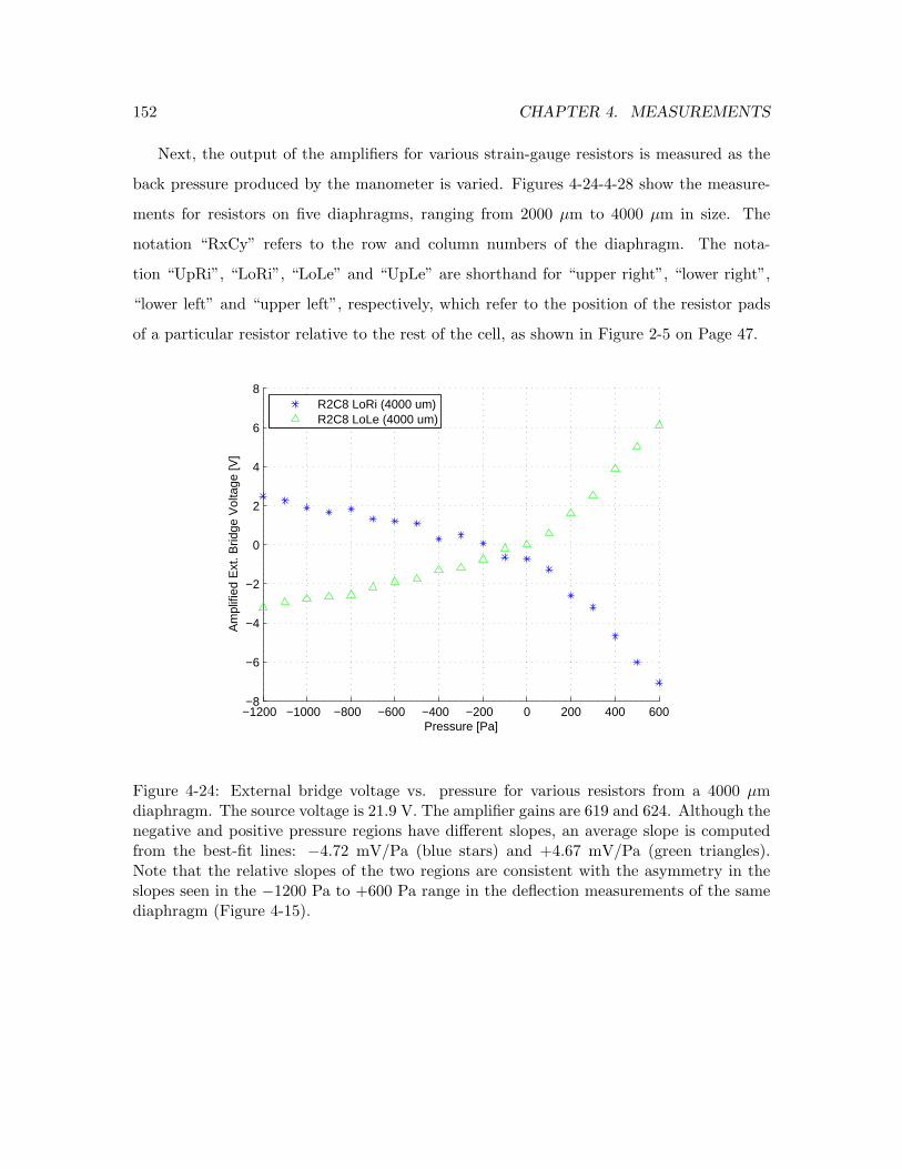
152 CHAPTER 4. MEASUREMENTS
Next, the output of the amplifiers for various strain-gauge resistors is measured as the
back pressure produced by the manometer is varied. Figures 4-24-4-28 show the measure-
ments for resistors on five diaphragms, ranging from 2000 µm to 4000 µm in size. The
notation “RxCy” refers to the row and column numbers of the diaphragm. The nota-
tion “UpRi”, “LoRi”, “LoLe” and “UpLe” are shorthand for “upper right”, “lower right”,
“lower left” and “upper left”, respectively, which refer to the position of the resistor pads
of a particular resistor relative to the rest of the cell, as shown in Figure 2-5 on Page 47.
−1200 −1000 −800 −600 −400 −200 0 200 400 600−8
−6
−4
−2
0
2
4
6
8
Pressure [Pa]
Am
plifi
ed E
xt. B
ridge
Vol
tage
[V]
R2C8 LoRi (4000 um)R2C8 LoLe (4000 um)
Figure 4-24: External bridge voltage vs. pressure for various resistors from a 4000 µmdiaphragm. The source voltage is 21.9 V. The amplifier gains are 619 and 624. Although thenegative and positive pressure regions have different slopes, an average slope is computedfrom the best-fit lines: −4.72 mV/Pa (blue stars) and +4.67 mV/Pa (green triangles).Note that the relative slopes of the two regions are consistent with the asymmetry in theslopes seen in the −1200 Pa to +600 Pa range in the deflection measurements of the samediaphragm (Figure 4-15).
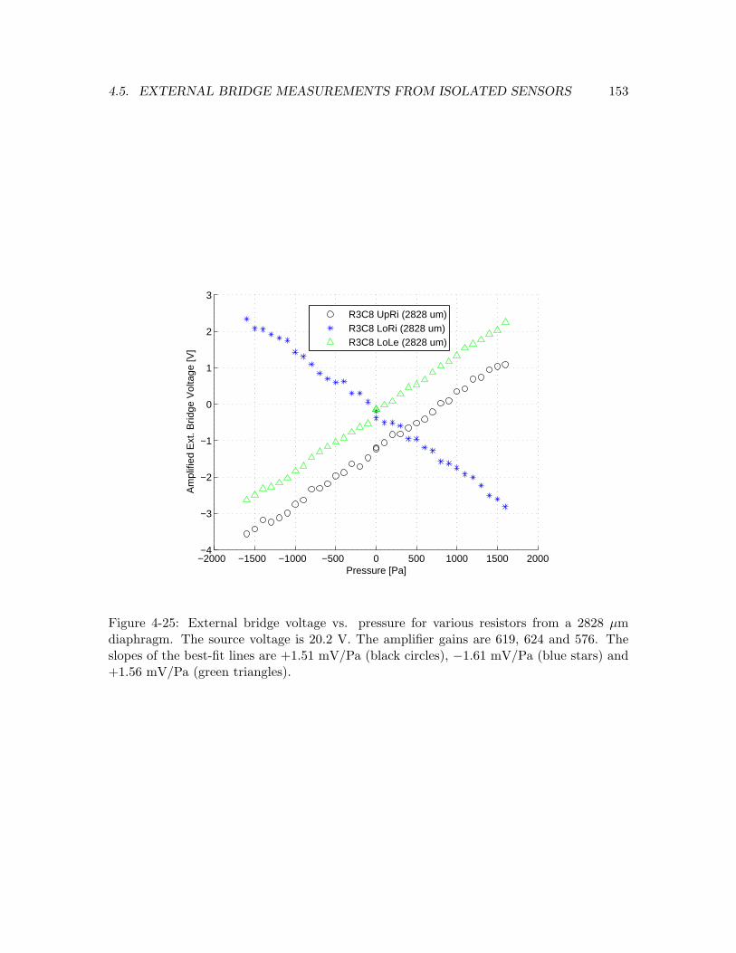
4.5. EXTERNAL BRIDGE MEASUREMENTS FROM ISOLATED SENSORS 153
−2000 −1500 −1000 −500 0 500 1000 1500 2000−4
−3
−2
−1
0
1
2
3
Pressure [Pa]
Am
plifi
ed E
xt. B
ridge
Vol
tage
[V]
R3C8 UpRi (2828 um)R3C8 LoRi (2828 um)R3C8 LoLe (2828 um)
Figure 4-25: External bridge voltage vs. pressure for various resistors from a 2828 µmdiaphragm. The source voltage is 20.2 V. The amplifier gains are 619, 624 and 576. Theslopes of the best-fit lines are +1.51 mV/Pa (black circles), −1.61 mV/Pa (blue stars) and+1.56 mV/Pa (green triangles).
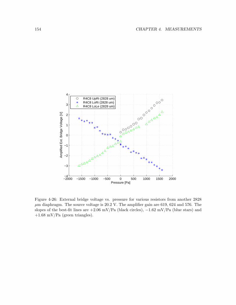
154 CHAPTER 4. MEASUREMENTS
−2000 −1500 −1000 −500 0 500 1000 1500 2000−4
−3
−2
−1
0
1
2
3
4
Pressure [Pa]
Am
plifi
ed E
xt. B
ridge
Vol
tage
[V]
R4C8 UpRi (2828 um)R4C8 LoRi (2828 um)R4C8 LoLe (2828 um)
Figure 4-26: External bridge voltage vs. pressure for various resistors from another 2828µm diaphragm. The source voltage is 20.2 V. The amplifier gain are 619, 624 and 576. Theslopes of the best-fit lines are +2.06 mV/Pa (black circles), −1.62 mV/Pa (blue stars) and+1.68 mV/Pa (green triangles).
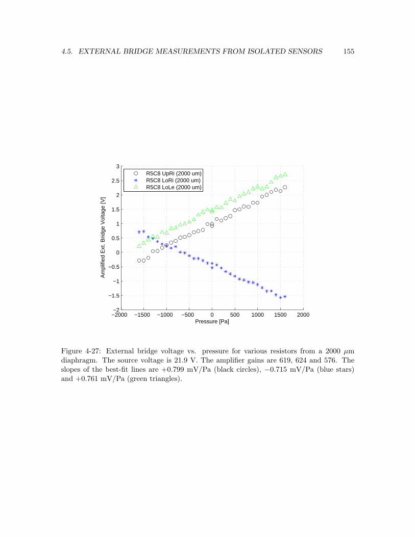
4.5. EXTERNAL BRIDGE MEASUREMENTS FROM ISOLATED SENSORS 155
−2000 −1500 −1000 −500 0 500 1000 1500 2000−2
−1.5
−1
−0.5
0
0.5
1
1.5
2
2.5
3
Pressure [Pa]
Am
plifi
ed E
xt. B
ridge
Vol
tage
[V]
R5C8 UpRi (2000 um)R5C8 LoRi (2000 um)R5C8 LoLe (2000 um)
Figure 4-27: External bridge voltage vs. pressure for various resistors from a 2000 µmdiaphragm. The source voltage is 21.9 V. The amplifier gains are 619, 624 and 576. Theslopes of the best-fit lines are +0.799 mV/Pa (black circles), −0.715 mV/Pa (blue stars)and +0.761 mV/Pa (green triangles).
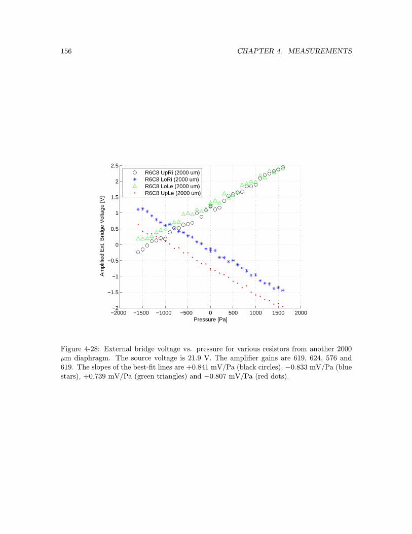
156 CHAPTER 4. MEASUREMENTS
−2000 −1500 −1000 −500 0 500 1000 1500 2000−2
−1.5
−1
−0.5
0
0.5
1
1.5
2
2.5
Pressure [Pa]
Am
plifi
ed E
xt. B
ridge
Vol
tage
[V]
R6C8 UpRi (2000 um)R6C8 LoRi (2000 um)R6C8 LoLe (2000 um)R6C8 UpLe (2000 um)
Figure 4-28: External bridge voltage vs. pressure for various resistors from another 2000µm diaphragm. The source voltage is 21.9 V. The amplifier gains are 619, 624, 576 and619. The slopes of the best-fit lines are +0.841 mV/Pa (black circles), −0.833 mV/Pa (bluestars), +0.739 mV/Pa (green triangles) and −0.807 mV/Pa (red dots).
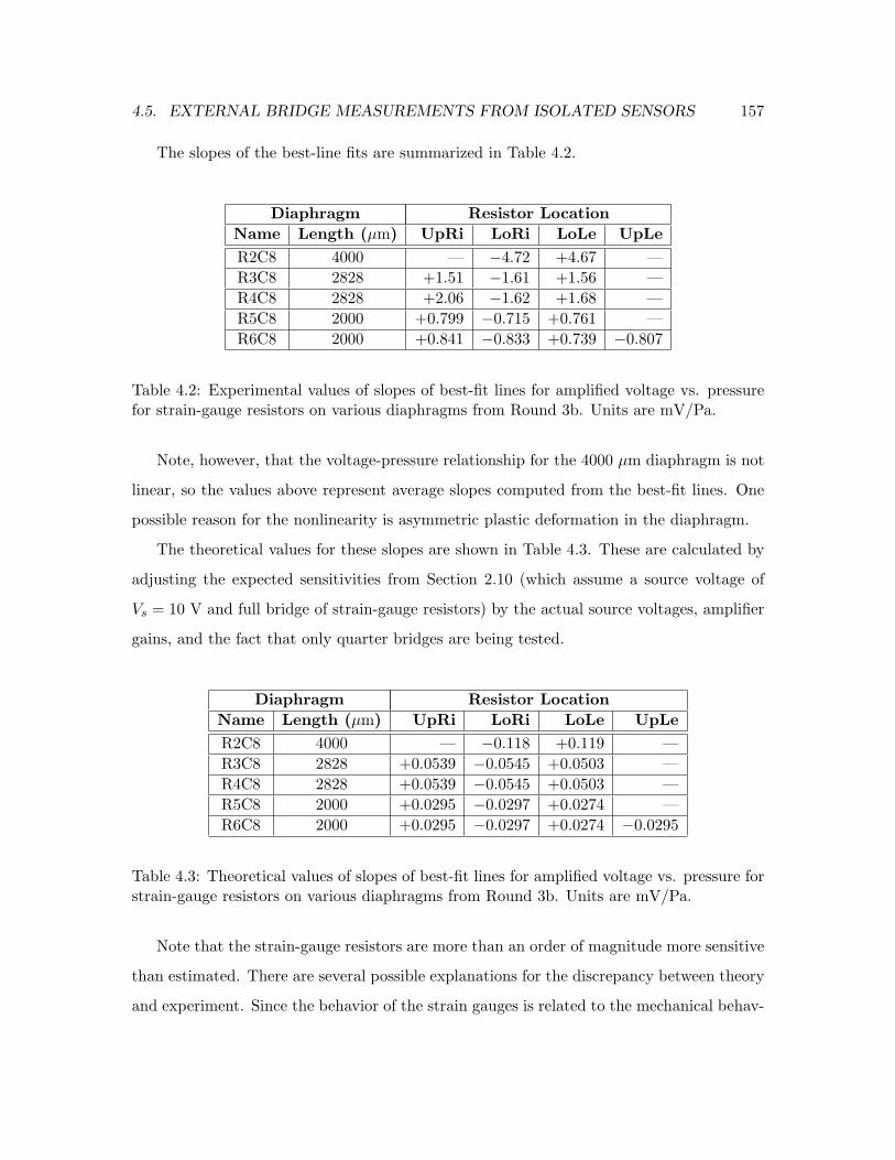
4.5. EXTERNAL BRIDGE MEASUREMENTS FROM ISOLATED SENSORS 157
The slopes of the best-line fits are summarized in Table 4.2.
Diaphragm Resistor Location
Name Length (µm) UpRi LoRi LoLe UpLe
R2C8 4000 — −4.72 +4.67 —
R3C8 2828 +1.51 −1.61 +1.56 —
R4C8 2828 +2.06 −1.62 +1.68 —
R5C8 2000 +0.799 −0.715 +0.761 —
R6C8 2000 +0.841 −0.833 +0.739 −0.807
Table 4.2: Experimental values of slopes of best-fit lines for amplified voltage vs. pressurefor strain-gauge resistors on various diaphragms from Round 3b. Units are mV/Pa.
Note, however, that the voltage-pressure relationship for the 4000 µm diaphragm is not
linear, so the values above represent average slopes computed from the best-fit lines. One
possible reason for the nonlinearity is asymmetric plastic deformation in the diaphragm.
The theoretical values for these slopes are shown in Table 4.3. These are calculated by
adjusting the expected sensitivities from Section 2.10 (which assume a source voltage of
Vs = 10 V and full bridge of strain-gauge resistors) by the actual source voltages, amplifier
gains, and the fact that only quarter bridges are being tested.
Diaphragm Resistor Location
Name Length (µm) UpRi LoRi LoLe UpLe
R2C8 4000 — −0.118 +0.119 —
R3C8 2828 +0.0539 −0.0545 +0.0503 —
R4C8 2828 +0.0539 −0.0545 +0.0503 —
R5C8 2000 +0.0295 −0.0297 +0.0274 —
R6C8 2000 +0.0295 −0.0297 +0.0274 −0.0295
Table 4.3: Theoretical values of slopes of best-fit lines for amplified voltage vs. pressure forstrain-gauge resistors on various diaphragms from Round 3b. Units are mV/Pa.
Note that the strain-gauge resistors are more than an order of magnitude more sensitive
than estimated. There are several possible explanations for the discrepancy between theory
and experiment. Since the behavior of the strain gauges is related to the mechanical behav-
158 CHAPTER 4. MEASUREMENTS
ior, the explanations mentioned in the Section 4.3 regarding the deflection measurements
apply here as well:
• Oxide grown and metal deposited on the diaphragm may have pre-stressed the di-
aphragms;
• Overetching the silicon device layer may have thinned the diaphragms;
• The actual diaphragm lengths may be longer and wider than the nominal design
values.
One other explanation could account for the remainder. The metal films that form the
resistors may have micro-cracks from the diaphragm deflecting or other sources. These
cracks consist of metal surfaces in contact with one another. Not only would resistance be
concentrated at these points, but the local resistance there would be extremely sensitive
to the relative motion of the surfaces. As the diaphragm deflects, more or fewer of the
cracks come into contact, which is manifested in the changes in the resistance of the total
strain-gauge resistor as a continuous phenomenon.
In any case, the sensitivity of the sensor is better than we had designed them to be.
Importantly, the results are consistent and do not change over time, which means the
pressure sensor can be calibrated. After taking the amplification, the 21.9 V source voltage,
and the use of a quarter Wheatstone bridge into account, the sensitivity of a full bridge
sensor on a 2000 µm diaphragm powered by a 10 V source ranges from 2.1 to 2.5 µV/Pa,
which is greater than the 0.087 µV/Pa expected by the device model (Sections 2.6 and 2.10),
and less than the 19.0 µV/Pa achieved by a physically comparable standard piezoresistive
pressure sensor (Section 2.5). With a noise level of 0.13 µV (Section 2.10), the sensor can
achieve sub-pascal resolution after appropriate mechanical and digital filtering is performed
on pressure signals.
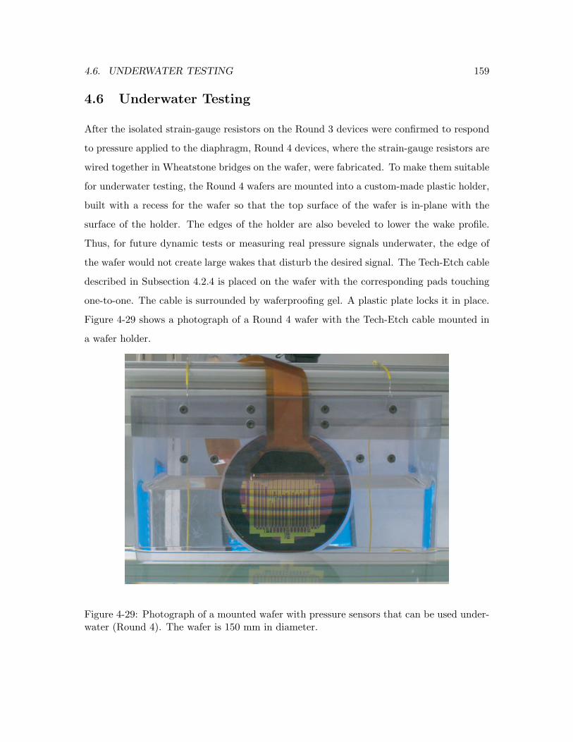
4.6. UNDERWATER TESTING 159
4.6 Underwater Testing
After the isolated strain-gauge resistors on the Round 3 devices were confirmed to respond
to pressure applied to the diaphragm, Round 4 devices, where the strain-gauge resistors are
wired together in Wheatstone bridges on the wafer, were fabricated. To make them suitable
for underwater testing, the Round 4 wafers are mounted into a custom-made plastic holder,
built with a recess for the wafer so that the top surface of the wafer is in-plane with the
surface of the holder. The edges of the holder are also beveled to lower the wake profile.
Thus, for future dynamic tests or measuring real pressure signals underwater, the edge of
the wafer would not create large wakes that disturb the desired signal. The Tech-Etch cable
described in Subsection 4.2.4 is placed on the wafer with the corresponding pads touching
one-to-one. The cable is surrounded by waferproofing gel. A plastic plate locks it in place.
Figure 4-29 shows a photograph of a Round 4 wafer with the Tech-Etch cable mounted in
a wafer holder.
Figure 4-29: Photograph of a mounted wafer with pressure sensors that can be used under-water (Round 4). The wafer is 150 mm in diameter.
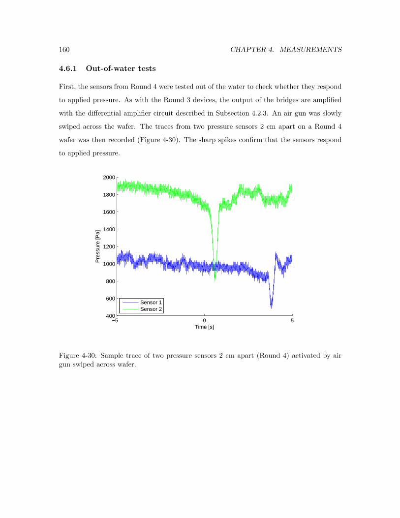
160 CHAPTER 4. MEASUREMENTS
4.6.1 Out-of-water tests
First, the sensors from Round 4 were tested out of the water to check whether they respond
to applied pressure. As with the Round 3 devices, the output of the bridges are amplified
with the differential amplifier circuit described in Subsection 4.2.3. An air gun was slowly
swiped across the wafer. The traces from two pressure sensors 2 cm apart on a Round 4
wafer was then recorded (Figure 4-30). The sharp spikes confirm that the sensors respond
to applied pressure.
−5 0 5400
600
800
1000
1200
1400
1600
1800
2000
Time [s]
Pre
ssur
e [P
a]
Sensor 1Sensor 2
Figure 4-30: Sample trace of two pressure sensors 2 cm apart (Round 4) activated by airgun swiped across wafer.
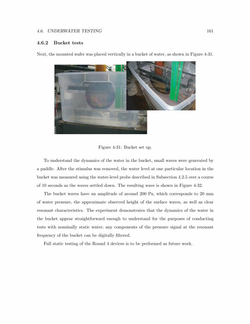
4.6. UNDERWATER TESTING 161
4.6.2 Bucket tests
Next, the mounted wafer was placed vertically in a bucket of water, as shown in Figure 4-31.
Figure 4-31: Bucket set up.
To understand the dynamics of the water in the bucket, small waves were generated by
a paddle. After the stimulus was removed, the water level at one particular location in the
bucket was measured using the water-level probe described in Subsection 4.2.5 over a course
of 10 seconds as the waves settled down. The resulting wave is shown in Figure 4-32.
The bucket waves have an amplitude of around 200 Pa, which corresponds to 20 mm
of water pressure, the approximate observed height of the surface waves, as well as clear
resonant characteristics. The experiment demonstrates that the dynamics of the water in
the bucket appear straightforward enough to understand for the purposes of conducting
tests with nominally static water; any components of the pressure signal at the resonant
frequency of the bucket can be digitally filtered.
Full static testing of the Round 4 devices is to be performed as future work.
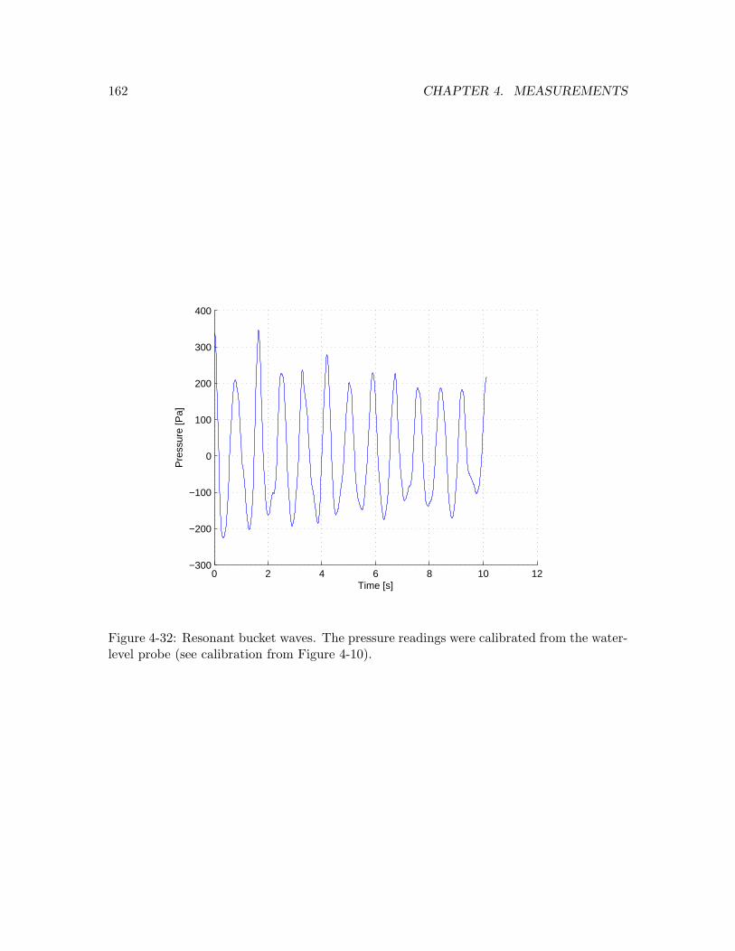
162 CHAPTER 4. MEASUREMENTS
0 2 4 6 8 10 12−300
−200
−100
0
100
200
300
400
Time [s]
Pre
ssur
e [P
a]
Figure 4-32: Resonant bucket waves. The pressure readings were calibrated from the water-level probe (see calibration from Figure 4-10).
4.7. SUMMARY OF MEASUREMENTS 163
4.7 Summary of Measurements
The results of the experiments in this chapter is summarized as follows.
Both the deflection and strain-gauge resistance measurements indicated that the sensor
is more sensitive than the designed nominal values. The factor of 2 to 3 in the deflection
can be attributed to several sources (Section 4.3):
• Compressive stress on the grown insulating silicon oxide film;
• Overetching of the diaphragm thickness;
• Angular misalignment of the devices features with the crystalline plane;
• The assumption of ideal clamping at the edges of the diaphragm;
• Manufacturing variation in the thickness of the handle wafer.
The compressive stress is by far the greatest effect, and could by itself account for all of the
discrepency between the model described in Section 2.6 and the experiments in this chapter.
The overetching of the diaphragm could alter the deflection by about 37%. Finally, each of
the other factors could contribute a few percent to the deflection as well.
The strain-gauge resistance measurements were, in turn, more sensitive than the deflec-
tion model would indicate, even after taking the factors above into account (Section 4.5).
Micro-cracks in the resistors, which appear with bending thin metal films, could account
for this remaining difference. A full bridge sensor on a 2000 µm diaphragm powered by a
10 V source has a sensitivity of 2.1 to 2.5 µV/Pa in the −2000 to 2000 Pa pressure range.
With a noise level of 0.13 µV (Section 2.10), the sensor can achieve sub-pascal resolution
after appropriate mechanical and digital filtering is performed on pressure signals.
Due to the existence of native chromium oxide, it is difficult to maintain a stable contact
resistance between external microscope probe tips and thin chromium pads (Section 4.4).
While the contact resistance can be stabilized with electrical and mechanical epoxies, the
process is time-consuming and may not be permanent. Thus, Round 4 devices, gold was
deposited on the chromium film under the same deposition vacuum to create a reliable inert
contact.

164 CHAPTER 4. MEASUREMENTS
Finally, preliminary tests with Round 4 devices indicated that sensors consisting of
strain-gauge resistors wired up on-wafer powered by wafer-level conduction lines do indeed
respond to changes in local external pressure (Section 4.6). Analysis of the surface waves
in a small bucket of water showed that the dynamics of the waves can be filtered from
pressure signals produced by underwater sensors to confirm their operation in nominally
static water.
Chapter 5
Concluding Remarks
This chapter consists of three parts. Section 5.1 summarizes the results of this thesis, in-
cluding lessons learned from the design, fabrication and testing of the strain-gauge pressure
sensors. Section 5.2 discusses the contributions and conclusions made by this thesis in the
areas of literature review, development of experimental techniques, fabrication and packag-
ing observations, and MEMS applications. Finally, Section 5.3 suggests several directions
for future work and explains how weaknesses can be addressed, such as improving the strain-
gauge resign, adding an integrated amplifier and array read-out circuit to the devices, and
fabricating pressure sensors using flexible materials.
165
166 CHAPTER 5. CONCLUDING REMARKS
5.1 Summary
This thesis presented the design, fabrication and testing of a high-density array of mi-
croelectromechanical systems (MEMS) pressure sensors inspired by the fish lateral line to
enable passive navigation by autonomous undersea vehicles (AUVs). We demonstrated the
feasibility of using a strain-gauge resistive silicon pressure sensor system with the device
performance parameters necessary to measure pressure signatures that enable signal pro-
cessing software on an AUV to detect and identify nearby objects (Chapter 1). While the
devices were implemented in silicon, all the technology used is transferrable to flexible ma-
terials, such as polymers, which enables future generations of devices to be placed flush
against the curved surfaces, such as fins and hulls. For this reason, pressure sensors using
the piezoresistive properties of silicon were not considered.
Several rounds of devices were designed to test various combinations of device features
(Chapter 2), including a diaphragm that deflects in response to pressure, resistors that act as
strain gauges in response to the mechanical strain on the diaphragm, and air channels that
connect the diaphragm cavities to the environment to remove the large-signal component
of pressure change. A mechanical model of the diaphragm based on Kirchhoff-Love plate
theory was developed to aid the design of the strain-gauge resistors that form the basis of
the pressure sensor system and to characterize the dynamic response of the sensor. The
designed performance parameters exceeded those required by AUV navigation.
The various rounds of devices were fabricated using standard integrated circuit (IC)
technologies (Chapter 3). Techniques for etching silicon using potassium hydroxide (KOH)
and etching Pyrex glass using solutions based on hydrofluoric acid (HF) were developed.
The design issues in the material selection, process flow, and mask layout were explored
and resolved.
Finally, the strain-gauge pressure sensors were tested (Chapter 4). We showed that
square silicon diaphragms of sizes between 1000 µm and 4000 µm with thickness 20 µm can
act as pressure sensors with the range and sentivity required for underwater object detec-
tion. Although compressive stress on grown thin oxide films, over-etching of the diaphragms,
simplifications in modeling the diaphragm length, and micro-cracks in the strain-gauge re-

5.1. SUMMARY 167
sistors may have increased sensitivity, the behavior of deflection and resistors are consistent
over time and display no hysteretic effects, which means that the system can be reliably
calibrated. Preliminary tests verified that the strain-gauge pressure sensor system can be
successfully tested and used underwater.

168 CHAPTER 5. CONCLUDING REMARKS
5.2 Contributions and Conclusions
In the course of the theoretical and experimental work that culminated in this thesis, re-
search was conducted in several areas. The contributions of this thesis are as follows.
• A literature review of published work on:
– The fish lateral line organ and biomimetics (Section 1.1);
– MEMS pressure sensors (Section 1.2);
– The small-deflection behavior of thin square diaphragms (Section 2.6);
– Pyrex etching (Section 3.5);
– The anisotropy of silicon as it relates to mechanical elasticity and etching (Sec-
tions 2.3, 2.6 and 3.4).
• The development of experimental techniques for:
– KOH-etching one side of a silicon wafer (Section 3.4);
– Etching Pyrex protected with a chromium/gold mask using an HF-based solution
(Section 3.5).
• Fabrication and packaging observations:
– KOH-etching a silicon wafer more than once, especially if one of the etches en-
velopes the entire wafer, renders the wafer physically fragile and prone to break-
ing in subsequent fabrication steps (Section 3.4).
– It is possible to anodically bond silicon and Pyrex wafers through a 3000 A layer
of silicon nitride (Section 3.6). Even though the silicon has been etched by KOH
and the Pyrex has been etched by an HF-based etchant, there are few enough
pinholes that air-tight seals can be formed.
– Removing silicon nitride using hot phosphoric acid is a thermally stressful pro-
cedure and should be avoided if possible (Section 3.6).

5.2. CONTRIBUTIONS AND CONCLUSIONS 169
– It is difficult to make stable electrical contacts with chromium pads due to the
presence of a thin chromium oxide layer that grows on the pads upon exposure
to air (Section 4.4). Thus, chromium deposition should be immediately followed
by gold deposition under the same vacuum. Not only is gold inert in air, but it
serves as an excellent conductor for external probes.
– Parylene can waterproof and insulate metal resistors (Section 4.6).
• Achieved pressure sensor specifications:
– Millimeter-scale spacing;
– Sensitivity of 2.1 to 2.5 µV/Pa (before amplification);
– Sub-pascal pressure resolution;
– Range at least −2000 Pa to 2000 Pa.
• MEMS applications:
– Created wafer-sized air channels for back pressure equilibration;
– Developed a novel strain-gauge resistor design;
– Successfully constructed a wafer-sized MEMS sensor system;
– Demonstrated the feasibility of using a strain-gauge pressure sensor for under-
water navigation applications;
– Motivated research in techniques for developing flexible polymer pressure sensors.
170 CHAPTER 5. CONCLUDING REMARKS
5.3 Future Work
There are several directions that future work on the pressure sensors described in this thesis
may take. From the short- to long-term, they are as follows.
• Further testing of Round 4 devices (fully interconnected strain-gauge sensors without
amplifying transistors);
• Improved strain-gauge design;
• Integrated amplifier and array read-out circuitry;
• Printed electronics on flexible substrates.
5.3.1 Further testing of Round 4 devices
To complete the characterization of Round 4 devices (fully interconnected strain-gauge
sensors without amplifying transistors), several tests are to be performed:
• Measure the static response of several sensors as the wafer is lowered, raised and tilted
in water with the air channel plugged;
• Repeat static tests with air channel open to the water environment to test the large-
signal filter;
• Measure the frequency response of several sensors using a hydrophone producing si-
nusoidal waves of single frequences;
• Obtain pressure signatures of moving objects passing a stationary sensor in stationary
water, stationary objects passing a moving sensor in stationary water, and stationary
objects near a stationary sensor in a constant flow.
5.3.2 Improved strain-gauge design
The strain-gauge resistors described in this thesis have the following characteristics (Sec-
tion 2.7):
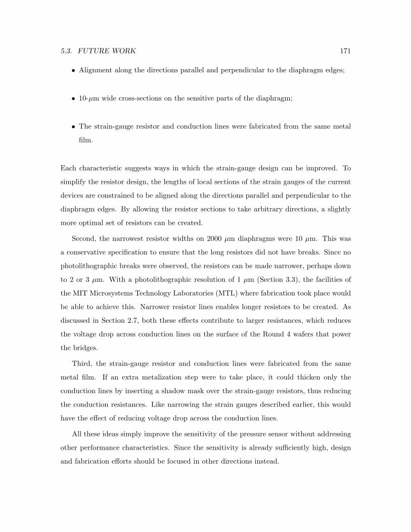
5.3. FUTURE WORK 171
• Alignment along the directions parallel and perpendicular to the diaphragm edges;
• 10-µm wide cross-sections on the sensitive parts of the diaphragm;
• The strain-gauge resistor and conduction lines were fabricated from the same metal
film.
Each characteristic suggests ways in which the strain-gauge design can be improved. To
simplify the resistor design, the lengths of local sections of the strain gauges of the current
devices are constrained to be aligned along the directions parallel and perpendicular to the
diaphragm edges. By allowing the resistor sections to take arbitrary directions, a slightly
more optimal set of resistors can be created.
Second, the narrowest resistor widths on 2000 µm diaphragms were 10 µm. This was
a conservative specification to ensure that the long resistors did not have breaks. Since no
photolithographic breaks were observed, the resistors can be made narrower, perhaps down
to 2 or 3 µm. With a photolithographic resolution of 1 µm (Section 3.3), the facilities of
the MIT Microsystems Technology Laboratories (MTL) where fabrication took place would
be able to achieve this. Narrower resistor lines enables longer resistors to be created. As
discussed in Section 2.7, both these effects contribute to larger resistances, which reduces
the voltage drop across conduction lines on the surface of the Round 4 wafers that power
the bridges.
Third, the strain-gauge resistor and conduction lines were fabricated from the same
metal film. If an extra metalization step were to take place, it could thicken only the
conduction lines by inserting a shadow mask over the strain-gauge resistors, thus reducing
the conduction resistances. Like narrowing the strain gauges described earlier, this would
have the effect of reducing voltage drop across the conduction lines.
All these ideas simply improve the sensitivity of the pressure sensor without addressing
other performance characteristics. Since the sensitivity is already sufficiently high, design
and fabrication efforts should be focused in other directions instead.
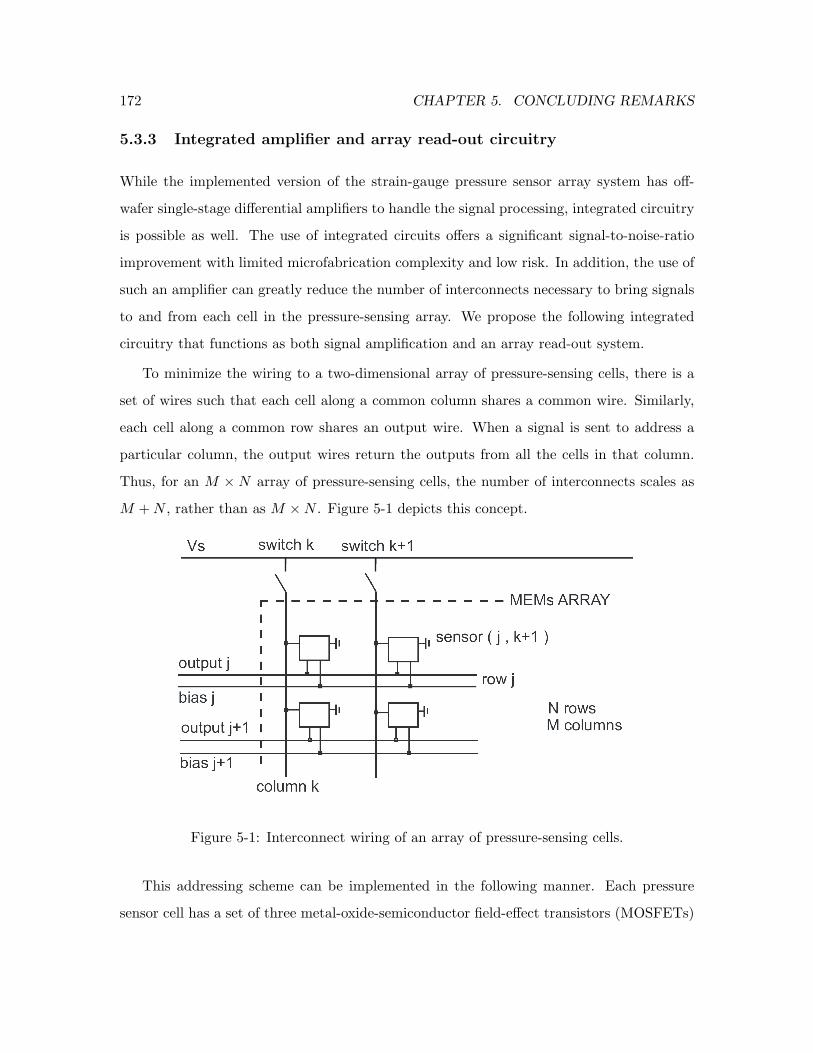
172 CHAPTER 5. CONCLUDING REMARKS
5.3.3 Integrated amplifier and array read-out circuitry
While the implemented version of the strain-gauge pressure sensor array system has off-
wafer single-stage differential amplifiers to handle the signal processing, integrated circuitry
is possible as well. The use of integrated circuits offers a significant signal-to-noise-ratio
improvement with limited microfabrication complexity and low risk. In addition, the use of
such an amplifier can greatly reduce the number of interconnects necessary to bring signals
to and from each cell in the pressure-sensing array. We propose the following integrated
circuitry that functions as both signal amplification and an array read-out system.
To minimize the wiring to a two-dimensional array of pressure-sensing cells, there is a
set of wires such that each cell along a common column shares a common wire. Similarly,
each cell along a common row shares an output wire. When a signal is sent to address a
particular column, the output wires return the outputs from all the cells in that column.
Thus, for an M × N array of pressure-sensing cells, the number of interconnects scales as
M +N , rather than as M ×N . Figure 5-1 depicts this concept.
Figure 5-1: Interconnect wiring of an array of pressure-sensing cells.
This addressing scheme can be implemented in the following manner. Each pressure
sensor cell has a set of three metal-oxide-semiconductor field-effect transistors (MOSFETs)
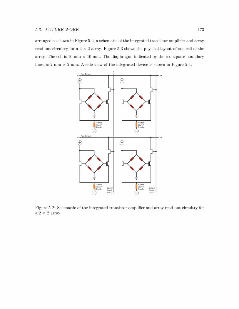
5.3. FUTURE WORK 173
arranged as shown in Figure 5-2, a schematic of the integrated transistor amplifier and array
read-out circuitry for a 2 × 2 array. Figure 5-3 shows the physical layout of one cell of the
array. The cell is 10 mm × 10 mm. The diaphragm, indicated by the red square boundary
lines, is 2 mm × 2 mm. A side view of the integrated device is shown in Figure 5-4.
"Current
Source"
ResistorColumn
Select
(Input)
Row Output
"Current
Source"
Resistor
"Current
Source"
ResistorColumn
Select
(Input)
"Current
Source"
Resistor
Row Output
Figure 5-2: Schematic of the integrated transistor amplifier and array read-out circuitry fora 2 × 2 array.
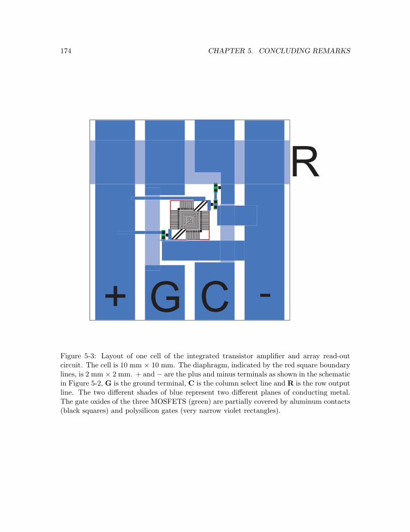
174 CHAPTER 5. CONCLUDING REMARKS
+ G C -
R
Figure 5-3: Layout of one cell of the integrated transistor amplifier and array read-outcircuit. The cell is 10 mm × 10 mm. The diaphragm, indicated by the red square boundarylines, is 2 mm × 2 mm. + and − are the plus and minus terminals as shown in the schematicin Figure 5-2, G is the ground terminal, C is the column select line and R is the row outputline. The two different shades of blue represent two different planes of conducting metal.The gate oxides of the three MOSFETS (green) are partially covered by aluminum contacts(black squares) and polysilicon gates (very narrow violet rectangles).
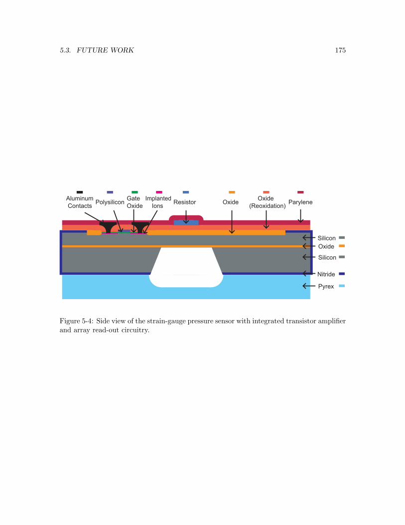
5.3. FUTURE WORK 175
Pyrex
Silicon
Nitride
Oxide
Silicon
Resistor Oxide ParyleneImplanted
Ions
Gate
Oxide
Aluminum
ContactsPolysilicon
Oxide
(Reoxidation)
Figure 5-4: Side view of the strain-gauge pressure sensor with integrated transistor amplifierand array read-out circuitry.

176 CHAPTER 5. CONCLUDING REMARKS
In the first generation of this device, the wafer would have a 5 × 5 array of sensors,
each occupying a 10 mm × 10 mm cell. This gives each cell plenty of real estate on the
wafer to reduce conduction line resistance and build physically large transistors to ensure
their reliability. Like with the Round 4 devices, all the diaphragms on a wafer would share
a common air cavity via a snaking air channel etched in the Pyrex wafer.
The process flow for the integrated pressure sensor is longer than the devices fabricated
for this thesis, but is not much more complex. It combines standard transistor fabrication
with the fabrication process described in Section 3.1 with no additional steps. First, the
Pyrex wafer are prepared as before. Next, silicon nitride is deposited on the SOI wafer
and most of the front-side is removed while a protective nitride ring (Subsection 3.4.3) is
retained. This is followed by a standard four-mask transistor fabrication routine:
• Field oxidation for transistors;
• Pattern active area;
• Gate oxidation for transistors;
• Create polysilicon gate;
• Reoxidation/activation;
• Pattern contact holes;
• Add aluminum contacts.
The remainder of the strain-gauge pressure sensor fabrication then takes place:
• KOH etch to release diaphragms;
• Bond Pyrex and SOI wafers;
• Create resistors;
• Add Parylene.
5.3. FUTURE WORK 177
However, once the aluminum is deposited, piranha cannot be used. Thus, any cleaning
or photoresist stripping steps afterwards involving piranha are replaced by Nano-StripTM.
Placing transistor fabrication early in the process flow allows for the testing of dummy
transistors before the comparatively more straightforward but time-consuming KOH etching
step (which can only be done one wafer at a time, with each etch taking around 8 hours).
Appendix Section C.4 shows the complete fabrication process flow for the integrated
sensors.
5.3.4 Flexible substrates
As discussed in Chapter 1, while this thesis built a silicon-based sensor system, a device
fabricated from flexible materials would be beneficial for AUVs, which have curved surfaces
and be more robust in the mechanically rough undersea environment. Furthermore, the
abandonment of KOH-etching silicon removes the restriction that the diaphragms be rect-
angular. This would allow for more novel shapes and locations for pressure sensors in the
array.
Members of our research group recently presented progress towards creating an artificial
lateral line using an entirely elastomer material set to provide flexibility and waterproofing.
Typically, elastomer-based pressure sensors are limited by large hysteresis and low sensitiv-
ity, so they have been used mainly for tactile applications. [96] addresses this limitation by
adopting a MEMS-based sensor geometry. Each sensor consists of a polydimethysiloxane
(PDMS) diaphragm and a resistive strain gauge made of a conductive carbon black-PDMS
composite. A functional linear array of four sensors with a 15 mm center-to-center spac-
ing has been demonstrated to be capable of underwater operation with 1.5 Pa resolution.
However, it still suffers from hysteresis and has a repeatability of about 22% of the input
pressure signal amplitude, due to creep. A diagram and photograph of the elastomer-based
pressure sensors are shown in Figure 5-5.
The integrated amplifier and array read-out circuitry described earlier can also be im-
plemented in flexible polymer materials using organic transistors or other novel compo-
nents that do not require silicon. For example, other members of our group have recently
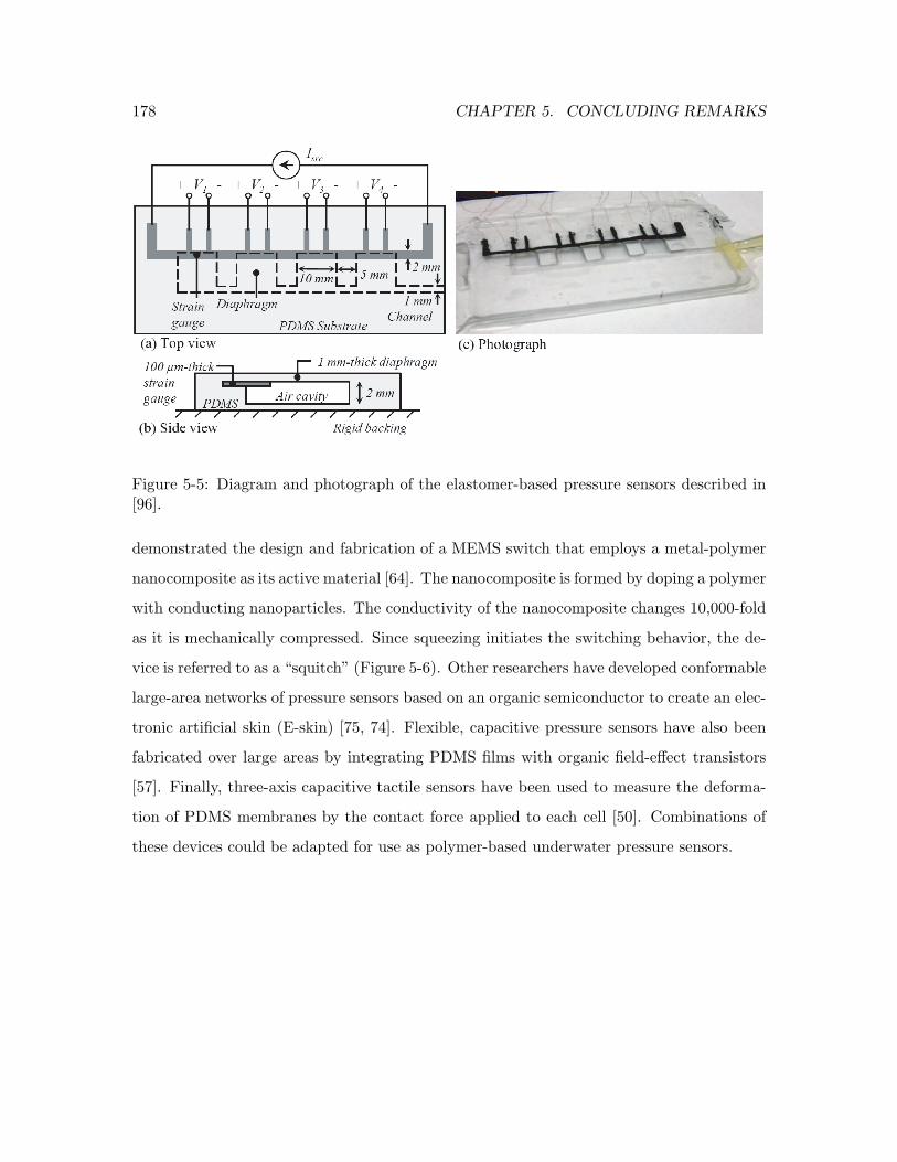
178 CHAPTER 5. CONCLUDING REMARKS
Figure 5-5: Diagram and photograph of the elastomer-based pressure sensors described in[96].
demonstrated the design and fabrication of a MEMS switch that employs a metal-polymer
nanocomposite as its active material [64]. The nanocomposite is formed by doping a polymer
with conducting nanoparticles. The conductivity of the nanocomposite changes 10,000-fold
as it is mechanically compressed. Since squeezing initiates the switching behavior, the de-
vice is referred to as a “squitch” (Figure 5-6). Other researchers have developed conformable
large-area networks of pressure sensors based on an organic semiconductor to create an elec-
tronic artificial skin (E-skin) [75, 74]. Flexible, capacitive pressure sensors have also been
fabricated over large areas by integrating PDMS films with organic field-effect transistors
[57]. Finally, three-axis capacitive tactile sensors have been used to measure the deforma-
tion of PDMS membranes by the contact force applied to each cell [50]. Combinations of
these devices could be adapted for use as polymer-based underwater pressure sensors.
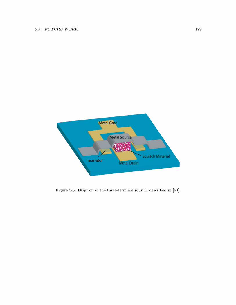
5.3. FUTURE WORK 179
Figure 5-6: Diagram of the three-terminal squitch described in [64].

180 CHAPTER 5. CONCLUDING REMARKS

Appendix A
Chemical Formulas
The chemical formulas for the common names and abbreviations of chemicals used in Ap-
pendices B and C are given in Table A.1.
Table A.1: Chemical formulas and full names.
Term Chemical Formula / Full Name Target Purpose
50:1 HF 50 H2O : 1 49% hydrofluoric acid (HF) Etches SiO2
Acetone (CH3)2CO Cleaning;strips PR
Aqua regia1 3 hydrochloric acid (HCl) : 1 nitric acid (HNO3) Etches gold
BOE Buffered oxide etch; 5 40% ammonium fluoride(NH4F) : 1 49% hydrofluoric acid (HF)
Etches SiO2
Cr-7 Chromium etchant; 9% (NH4)2Ce(NO3)6 +6%HClO4 +H2O
Etches chromium
Gold etchant TFA Gold etchant thin film type A; 30% potassiumiodide (KI), 1.3% iodine (I2), 68.7% water (H2O)
Etches gold
HMDS Hexamethyldisilazane; NH (Si (CH3)3)2 Adhesion for PR
Isopropanol; IPA (CH3)2CHOH Cleaning
Methanol CH3OH Cleaning
Piranha 3 sulfuric acid (H2SO4) : 1 hydrogen peroxide(H2O2)
Cleaning;strips PR
Phosphoric acid H3PO4 Etches Si3N4
PR Photoresist. AZ 917 was used for mask-making;OCG 934 for everything else.
Photolithographicmasking material
1Latin for “royal water”. It should not be confused with acquaragia, which is commonly known asturpentine in English.
181

182 APPENDIX A. CHEMICAL FORMULAS
Appendix B
Standard Operating Procedures
This appendix contains key standard operating procedures (SOPs) used for the process
flows in Appendix C. The relevant section of the main text that discusses each procedure
is indicated in parentheses.
• B.1: Mask-making (Section 3.3);
• B.2: TRL photolithography (Section 3.3);
• B.3: KOH etching (Section 3.4);
• B.4: Post-KOH clean (Section 3.4);
• B.5: Hot phosphoric (Section 3.6);
• B.6: EV501 and anodic bonding (Section 3.6).
The chemical formulas for the common names and abbreviations used are given in Ap-
pendix A. All processing was done at the MIT Microsystems Technology Laboratories
(MTL), which consists of three facilities: Technology Research Laboratory (TRL), Inte-
grated Circuits Laboratory (ICL) and Exploratory Materials Laboratory (EML).
183

184 APPENDIX B. STANDARD OPERATING PROCEDURES
B.1 Mask-Making
Approximate Time: 60 minutes
1. Cut out the transparency mask so that it is 7” by 7”.
2. Clean the glass plate near EV1 with acetone, methanol and isopropanol, in that order.
3. Create a stack in the following manner: Put the blank glass-chromium mask on thebottom with the chromium and PR side up. Put the transparency in the middle withthe ink side down. Finally, put the glass plate on top. The pattern is effectivelyupside-down compared to the usual mask usage.
4. Expose the stack on EV1 with flood exposure for 5.0 seconds.
5. Put the blank mask into a mask carrier.
6. Pour AZ 917 developer into a blue container.
7. Develop the blank mask in AZ 917 for 90 seconds. Let the mask sit in the developerfor 30 seconds before agitating.
8. Dump rinse and blow dry the mask.
9. In an acidhood, rinse out and blow dry the blue container. It is important that thecontainer is dry.
10. Pour Cr-7 into the blue container. Etch the exposed chromium on the mask for 90seconds.
11. Aspirate and clean the blue container.
12. Pour nanostrip into the blue container. Strip PR from the mask for 5 minutes.
13. Aspirate and clean the blue container.
14. Dump rinse and blow dry the mask.

B.2. TRL PHOTOLITHOGRAPHY 185
B.2 TRL Photolithography
Approximate Time: At least 2 hours
1. HMDS
(a) Load wafers into the metal boat. Be sure to use the correct (Au vs. non-Au)ones. Important: Do not put wafers that have PR on them in the HMDSmachine.
(b) Put the boat into the HMDS machine using the appropriate grip.
(c) Select recipe 5 and press “start”.
(d) After 20–25 minutes, the machine will emit a sound.
(e) Press reset and place boat in the glass dish to cool.
2. Coater
(a) Replace the coater wafer holder with a 6” one. Clean it with acetone and blowdry.
(b) Set the photoresist setting to 1.
(c) Hold the round wafer carrier in your left hand. Use your right hand to place thewafer on the round wafer carrier.
(d) Place the wafer on the wafer holder. Be sure that it is centered.
(e) Turn on the vacuum (when the vacuum light is on, the vacuum is off) andcarefully remove the wafer carrier without touching the wafer.
(f) Set the rightmost time settings to 9.0 s, 6 s and 30 s.
(g) Move the dispenser to the side and test run by pressing “start” to let the oldPR drip. Set the three speeds to 500 RPM, 750 RPM and 3000 RPM during thetest run. Make sure that the wafer is centered; if not, fix it.
(h) Move the dispenser over the wafer.
(i) Press “start”.
(j) While the dispenser is releasing PR, move it back and forth over the wafer.
(k) When the dispenser stops releasing PR and the wafer spins faster, move thedispenser to the side so that any further drips will not ruin the PR coat.
(l) When the wafer stops spinning, release the vacuum and use the round wafercarrier to move the wafer into the regular wafer boat.
(m) Repeat these steps for each wafer.
3. Pre-Bake
(a) Put the wafers in the 90C pre-bake oven for 30 minutes.
(b) Allow the wafers to cool.
186 APPENDIX B. STANDARD OPERATING PROCEDURES
(c) Important: If you are not exposing the wafers immediately, be sure to storethe wafers in a UV-free environment.
4. EV1
(a) Open the program using “g” as both the username and password.
(b) Select the appropriate recipe. Use the parameters “continuous,” “soft contact”and “2.3 s” exposure time. Most masks are 2.3mm thick. Be sure to enter thecorrect wafer thickness (standard is 650µm).
(c) Change the mask holder and wafer chuck for the appropriate size and colordesignation.
(d) Set the x, y and θ coordinates to (5, 5, 5).
(e) Henceforth, follow the instructions on the screen.
(f) Place the mask frame on the wafer chuck.
(g) Load the mask chromium side down.
(h) After the mask is in the machine, use the optics to locate key features. Storetheir coordinates.
(i) Remove the mask frame.
(j) Load the wafer on the wafer chuck.
(k) After the wafer is in the machine, use the optics to align features to the mask.
(l) Expose the wafer.
(m) Repeat for each wafer.
(n) When finished, exit, park, and log out.
5. Develop
(a) Fill a green round plastic container with OCG 934 1:1 developer.
(b) Put a wafer in the developer for 60 s. Gently move the container in circles anduse a wafer holder to move the wafer up and down. Be sure that the features arevisible.
(c) Rinse the wafer over the faucet.
(d) Dump the developer.
(e) Repeat above steps for each wafer.
(f) When all wafers are developed, dump rinse them together.
(g) Spin dry the wafers.
6. Post-Bake
(a) Put the wafers in the 120C post-bake oven for 30 minutes.
(b) Allow the wafers to cool.

B.2. TRL PHOTOLITHOGRAPHY 187
B.2.1 Double-sided PR
When both sides of a wafer are to be coated, but only one side is to be exposed, do thefollowing procedure.
1. HMDS
2. Spincoat PR on the side that won’t be exposed.
3. Prebake for 15 minutes.
4. Let the wafer cool.
5. Spincoat PR on the side that will be exposed.
6. Prebake for 30 minutes.
7. Expose to EV1.
8. Develop.
9. Post-bake for 30 minutes.
B.2.2 With paint
Spincoating PR does not cover the edge of the wafer. When complete coverage is necessary,additional PR is painted onto the edge before prebaking.
188 APPENDIX B. STANDARD OPERATING PROCEDURES
B.3 KOH Etching
Approximate Time: Varies
1. Put the wafers in a dedicated KOH transfer wafer box and bring them to EML, wherethe ICL TMAH-KOH station is located.
2. Gown up.
3. Turn on the hot bath and make sure the target temperature is set to 85C.
4. Fill the bath up with water with the spray gun so that the floating balls no longertouch the bars on the walls of the bath.
5. Take the glass square beaker out of the KOH cabinet below the station. Rinse it out.
6. Use the graduated cylinder from the same cabinet to put 3 L of water into the squarebeaker. Put the beaker in the bath. Make sure that the height of the bath waterexceeds that in the square beaker.
7. From the KOH cabinet to the right of the station, take out a plastic beaker. Put iton the electronic scale and zero it.
8. Take out bottles of KOH pellets from the lower cabinet to the right of the station.Pour KOH pellets into the plastic beaker until the scale reads 750 g.
9. Pour the KOH pellets into the square beaker. Use a wand to stir the mixture untilall of the KOH is dissolved.
10. Put the square lid over the square beaker so that water does not evaporate away. Putthe clear lid over the entire bath.
11. Put away the measuring equipment and wait until the bath temperature has reached80C. This takes about one hour.
12. Remove both layers of lids.
13. Put the wafers into a teflon wafer carrier.
14. Prepare a 50:1 HF solution using the 49% HF bottle from the acid room. Be sure thesolution is in a teflon container.
15. Place the wafers into the HF solution for 30 seconds to etch away any native oxide.
16. Place the wafers directly into the bath horizontally. If possible, place the wafersinto the middle slots.
17. Important: Put the lids back on the square beaker and the bath. Otherwise, waterwill evaporate and the KOH concentration in the beaker will change over time.

B.3. KOH ETCHING 189
18. A 20% KOH mixture at 80C etches at 80µm/min. Wait for the appropriate lengthof time.
19. When the etch is finished, take off the lids. Take the wafer carrier out of beaker andplace it in the cascade rinse. Turn on the rinse.
20. Drain the bath.
21. Pour out the square beaker containing the KOH solution. Rinse it thoroughly andput it back in the lower cabinet.
22. When the wafers have been thoroughly rinsed, turn off the cascade rinse and blow drythe wafers.
23. Examine the etch under the microscope.
24. Put the wafers back into the KOH transfer box. They are now ready for post-KOHclean.
25. Clean up the lab station.

190 APPENDIX B. STANDARD OPERATING PROCEDURES
B.4 Post-KOH Clean
Approximate Time: 90 minutes
1. Open the post-KOH clean box of wafers near Acidhood 1 before suiting up. Acidhood2 may not be used.
2. Suit up.
3. Get a yellow wafer boat (with gloves) and transfer wafers to the boat (without gloves).
4. Get a yellow plastic vat (for water only), a yellow glass vat, and a green glass vat.The glass vats will contain piranha, which is a 3:1 solution of sulfuric acid (H2SO4)and hydrogen peroxide (H2O2); the ratio does not have to be exact. Remember: Addacid.
5. Fill the yellow plastic vat with water from the sink.
6. Use a top-type yellow wafer handler to put the wafers in the yellow plastic vat.
7. Go to the acid storage and get a bottle of hydrogen peroxide and at least two fullbottles of sulfuric acid. Bring them to the acid hood.
8. Pour hydrogen peroxide into both glass vats so that the depth is 4–6 cm.
9. Add about three times the amount of sulfuric acid into both glass vats. The solutionsshould be warm and vapors should be forming.
10. Take the boat out of the yellow plastic vat and transfer it directly into the yellowglass vat. Begin 10-minute countdown.
11. Rinse the yellow plastic vat and return it to the shelf.
12. When the 10 minutes are up, place the boat in the dump rinser and set for 5 rinses.
13. Aspirate and clean the yellow glass vat.
14. Transfer the wafers from the yellow boat to a green boat.
15. Put the wafers into the green glass vat and begin the 10-minute countdown.
16. Prepare a 50:1 HF solution in a green plastic vat. Remember: Add acid.
17. When the 10 minutes are up, place the boat in the dump rinser and set for 5 rinses(second time).
18. Aspirate and clean the green glass vat.
19. Put the wafers into the HF solution for 30 seconds.
20. Place the boat in the dump rinser and set for 5 rinses (third time).

B.4. POST-KOH CLEAN 191
21. Aspirate and clean the green plastic vat.
22. Spin dry the wafers.
23. Clean up the acid station.

192 APPENDIX B. STANDARD OPERATING PROCEDURES
B.5 Hot Phosphoric
Approximate Time: 2–4 hours
B.5.1 ICL hot phosphoric
If the wafer is allowed in ICL (e.g. it is not in pieces), then use the dedicated hot phosphoricstation in ICL to remove nitride.
1. Suit up.
2. Check whether the acid goes up to the gray line. If not, ask Paul Tierney for help.
3. Press “on” and “reset” to heat up the bath to 165C. This takes about one hour.
4. Put the wafers in the dedicated wafer boat.
5. Hold the wafer boat above the acid for one minute to allow it to heat up slowly inthe vapors.
6. Slowly place the boat in the acid bath. Be sure that the wafer holder is orientedforward-back, not left-right.
7. Phosphoric acid (H3PO4) at 160C etches nitride at 50 A/min; let the wafers sit inthe bath for the appropriate period of time.
8. When the wafers are done, slowly take the boat out of the bath and hold the wafersabove the acid for one minute.
9. Place the boat on the counter for several minutes to allow the wafers to cool.
10. Run the dump rinse several times without the wafers.
11. Place the wafers in the dump rinse.
12. Do not spin dry the wafers because they might be fragile from KOH etching. Instead,blow dry them.
B.5.2 TRL acid hood
If the wafer is not allowed in ICL (e.g. it is in pieces), then use the TRL acid hood toremove nitride.
1. Fill a glass beaker with phosphoric acid.
2. Put the large hot plate in the acid hood. Put the beaker on it, plug in the hot plate,and turn it on.

B.5. HOT PHOSPHORIC 193
3. Place a thermometer in the beaker to monitor the temperature. Be sure that thethermometer’s range is well above 160C. Wait for the temperature to reach 160C,which will take about 2 hours.
4. Put the wafers in a boat.
5. Hold the wafer boat above the acid for one minute to allow it to heat up in slowlyin the vapors.
6. Slowly place the boat in the acid bath.
7. Phosphoric acid at 160C etches nitride at 50 A/min; let the wafers sit in the bathfor the appropriate period of time.
8. When the wafers are done, slowly take the boat out of the bath and hold the wafersabove the acid for one minute.
9. Place the boat on the counter for several minutes to allow the wafers to cool.
10. Run the dump rinse several times without the wafers.
11. Place the wafers in the dump rinse.
12. Aspirate the phosphoric acid.
13. Clean up the acid hood.

194 APPENDIX B. STANDARD OPERATING PROCEDURES
B.6 EV501 and Anodic Bonding
Approximate Time: Varies
1. Clean the SOI wafer and Pyrex wafer to be bonded in piranha for 10 minutes.
2. Clean all tooling with isopropanol (IPA) and fabwipes prior to using.
3. Put on a new pair of vinyl gloves immediately prior to the bonding sequence, afterthe cleaning step.
4. Transport the wafers from the cleaning station in the teflon boat in which the waferswere cleaned. Do NOT use metal tweezers.
5. Start by making sure the aligner x and y verniers are at the 5 µm mark, and adjustthe θ vernier correctly over the white square.
6. The SOI wafer is loaded first with the bonding surface and alignment marks facingDOWN.
7. The SOI wafer is then aligned via movable bottom mounted CCD cameras in the xdirection, and via verniers in the θ and y directions.
8. The SOI wafer is brought into vacuum contact with the bondchuck, and electronicallygenerated crosshairs are then positioned over the still visible crosshairs.
9. Insert wafer separation spacers called FLAGS, and then load the Pyrex wafer withbond surface facing UP, to mate with the SOI wafer. Note: the second wafer musthave alignment marks on the non-bonding surface, in addition to any which may beon the bonding surface.
10. The Pyrex wafer is moved, with verniers, to align with the electronic crosshair regis-ters, and the bond occurs with SDB, or the bondchuck clamps the loadframe / wafer/ flag / wafer stack in place, for bonding.
11. Use software program AB1 on the ”menu”, and the Au-compatible bondchuck, load-frame, and the GRAPHITE pressure diffuser, which will act as a cathode in thisprocess.
12. When installing the bondchuck, make absolutely sure the clamps are in their recesses.If not, they will break the $1500 quartz loadframe when contact is made.
13. Set thickness of the bonder to the combined wafer thickness plus 3 mm.
14. Place the stack in the bonder and lock it. The Pyrex is on top; the electrode puck isin contact with the Pyrex.
15. Turn on the bonder.

B.6. EV501 AND ANODIC BONDING 195
16. Start the recipe (see below).
17. When the process has terminated, wait for the bonder temerature to reach near roomtemperature.
18. Unlock the bonder and remove the bonded wafers.
19. Lock the bonder to keep it clean.
Table B.1: Recipe for bonding silicon and Pyrex.
Step Command Param 1 Param 2
1 Waferbow
2 Wait Time 0:00:20
3 Heating 350 0:00:00
4 Set temp. top 350
5 Wait Temp. bottom 350
6 Wait Temp. top 350
7 Wait Time 0:00:10
8 Flags out All
9 Wait Time 0:00:10
10 Piston down 2000
11 Voltage on Intern neg. 1000
12 Wait Time 0:05:00
13 Wait Current < 5
14 Wait Time 0:05:00
15 Voltage off
16 Piston up
17 Cooling 155 0:00:00
18 Wait Temp. top 200
19 Vent on
20 Wait Time 0:01:00
21 Purge off
22 ** END **

196 APPENDIX B. STANDARD OPERATING PROCEDURES
Appendix C
Process Flows
This appendix contains the process flows and recipes used. The photolithography process
flow was described beginning on Page 92 in Section 3.3. The remarks regarding the proce-
dure for finding the crystalline plane for (100) silicon can be found beginning on Page 117 in
Section 3.8. The Pyrex process flow shown as part of the device process flows is identical to
the one shown in Table 3.3 on Page 104. Diagrams and explanations of the device process
flows can be found beginning on Page 86 in Section 3.1. Discussion about the strain-gauge
silicon sensors with transistors can be found beginning on Page 170 in Section 5.3.
The chemical formulas for the common names and abbreviations used are given in Ap-
pendix A. Key standard operating procedures (SOPs) used for the process flows are given
in Appendix B. All processing was done at the MIT Microsystems Technology Labora-
tories (MTL), which consists of three facilities: Technology Research Laboratory (TRL),
Integrated Circuits Laboratory (ICL) and Exploratory Materials Laboratory (EML).
197

198 APPENDIX C. PROCESS FLOWS
C.1 Standard Photolithography
Tables C.1 and C.2 show the process flow for all single- and double-sided photolithography
procedures, respectively. For the double-sided photolithography, only one side is etched.
Table C.1: Process flow for standard single-sided photolithography.
Step Lab Machine Recipe Description
S.1 HMDS TRL HMDS Recipe 5 Coat both sides of wafers withHMDS
S.2 Coat PR TRL Coater PR 1; 500 RPM (9.0s), 750 RPM (6 s),3000 RPM (30 s)
Coat 1 µm positive photoresist(PR) on desired side of wafer
S.3 Pre-bake TRL Pre-bake 30 min Pre-bake PR at 90C
S.4 Expose TRL EV1 2.3 s Expose PR to UV light withmask
S.5 Develop TRL Develop hood OCG 934 1:1, 60 s Develop the PR
S.6 Post-bake TRL Post-bake 30 min Post-bake PR at 120C
Table C.2: Process flow for standard double-sided photolithography.
Step Lab Machine Recipe Description
D.1 HMDS TRL HMDS Recipe 5 Coat both sides of wafers withHMDS
D.2 Coat PR TRL Coater PR 1; 500 RPM (9.0s), 750 RPM (6 s),3000 RPM (30 s)
Coat 1 µm positive photore-sist (PR) on side of wafer thatwon’t be exposed
D.3 Pre-bake TRL Pre-bake 15 min Pre-bake PR at 90C
D.4 Coat PR TRL Coater PR 1; 500 RPM (9.0s), 750 RPM (6 s),3000 RPM (30 s)
Coat 1 µm positive photoresist(PR) on side of wafer that willbe exposed
D.5 Pre-bake TRL Pre-bake 30 min Pre-bake PR at 90C
D.6 Expose TRL EV1 2.3 s Expose PR to UV light withmask
D.7 Develop TRL Develop hood OCG 934 1:1, 60 s Develop the PR
D.8 Post-bake TRL Post-bake 30 min Post-bake PR at 120C
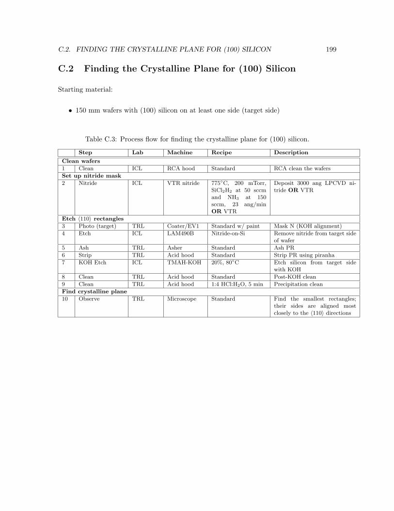
C.2. FINDING THE CRYSTALLINE PLANE FOR (100) SILICON 199
C.2 Finding the Crystalline Plane for (100) Silicon
Starting material:
• 150 mm wafers with (100) silicon on at least one side (target side)
Table C.3: Process flow for finding the crystalline plane for (100) silicon.
Step Lab Machine Recipe Description
Clean wafers
1 Clean ICL RCA hood Standard RCA clean the wafers
Set up nitride mask
2 Nitride ICL VTR nitride 775C, 200 mTorr,SiCl2H2 at 50 sccmand NH3 at 150sccm, 23 ang/minOR VTR
Deposit 3000 ang LPCVD ni-tride OR VTR
Etch 〈110〉 rectangles
3 Photo (target) TRL Coater/EV1 Standard w/ paint Mask N (KOH alignment)
4 Etch ICL LAM490B Nitride-on-Si Remove nitride from target sideof wafer
5 Ash TRL Asher Standard Ash PR
6 Strip TRL Acid hood Standard Strip PR using piranha
7 KOH Etch ICL TMAH-KOH 20%, 80C Etch silicon from target sidewith KOH
8 Clean TRL Acid hood Standard Post-KOH clean
9 Clean TRL Acid hood 1:4 HCl:H2O, 5 min Precipitation clean
Find crystalline plane
10 Observe TRL Microscope Standard Find the smallest rectangles;their sides are aligned mostclosely to the 〈110〉 directions

200 APPENDIX C. PROCESS FLOWS
C.3 Strain-Gauge Silicon Sensors Without Transistors
The following charts show the process flow for Round 4 devices. The manner in which the
process flows for Rounds 1, 2, 3a and 3b differ from that of Round 4 is explained at the end
of Section 3.1.
Starting materials:
• 150 mm SOI wafers: Double-side polished (100) silicon with 20 µm n-type epi-layer
• 150 mm Pyrex wafers: Corning Pyrex 7740
The process flow is arranged into the following tables:
• Table C.4 describes the preparation of Pyrex for bonding with SOI.
• Tables C.5 and C.6 describe partial sensor fabrication on SOI wafers. They are inde-
pendent of Table C.4.
• Table C.7 describes bonding of SOI with Pyrex and the remainder of the sensor
fabrication.
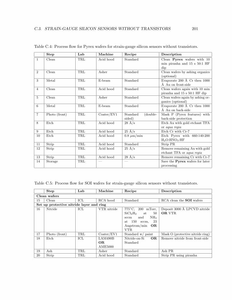
C.3. STRAIN-GAUGE SILICON SENSORS WITHOUT TRANSISTORS 201
Table C.4: Process flow for Pyrex wafers for strain-gauge silicon sensors without transistors.
Step Lab Machine Recipe Description
1 Clean TRL Acid hood Standard Clean Pyrex wafers with 10min piranha and 15 s 50:1 HFdip
2 Clean TRL Asher Standard Clean wafers by ashing organics(optional)
3 Metal TRL E-beam Standard Evaporate 200 A Cr then 1000A Au on front-side
4 Clean TRL Acid hood Standard Clean wafers again with 10 minpiranha and 15 s 50:1 HF dip
5 Clean TRL Asher Standard Clean wafers again by ashing or-ganics (optional)
6 Metal TRL E-beam Standard Evaporate 200 A Cr then 1000A Au on back-side
7 Photo (front) TRL Coater/EV1 Standard (double-sided)
Mask P (Pyrex features) withback-side protection
8 Etch TRL Acid hood 28 A/s Etch Au with gold etchant TFAor aqua regia
9 Etch TRL Acid hood 25 A/s Etch Cr with Cr-7
10 Etch TRL Acid hood 0.8 µm/min Etch Pyrex with 660:140:200H2O:HNO3:HF
11 Strip TRL Acid hood Standard Strip PR
12 Strip TRL Acid hood 25 A/s Remove remaining Au with goldetchant TFA or aqua regia
13 Strip TRL Acid hood 28 A/s Remove remaining Cr with Cr-7
14 Storage TRL — — Save the Pyrex wafers for laterprocessing
Table C.5: Process flow for SOI wafers for strain-gauge silicon sensors without transistors.
Step Lab Machine Recipe Description
Clean wafers
15 Clean ICL RCA hood Standard RCA clean the SOI wafers
Set up protective nitride layer and ring
16 Nitride ICL VTR nitride 775C, 200 mTorr,SiCl2H2 at 50sccm and NH3
at 150 sccm, 23Angstrom/min ORVTR
Deposit 3000 A LPCVD nitrideOR VTR
17 Photo (front) TRL Coater/EV1 Standard w/ paint Mask O (protective nitride ring)
18 Etch ICL LAM490BORAME5000
Nitride-on-Si ORStandard
Remove nitride from front-side
19 Ash TRL Asher Standard Ash PR
20 Strip TRL Acid hood Standard Strip PR using piranha
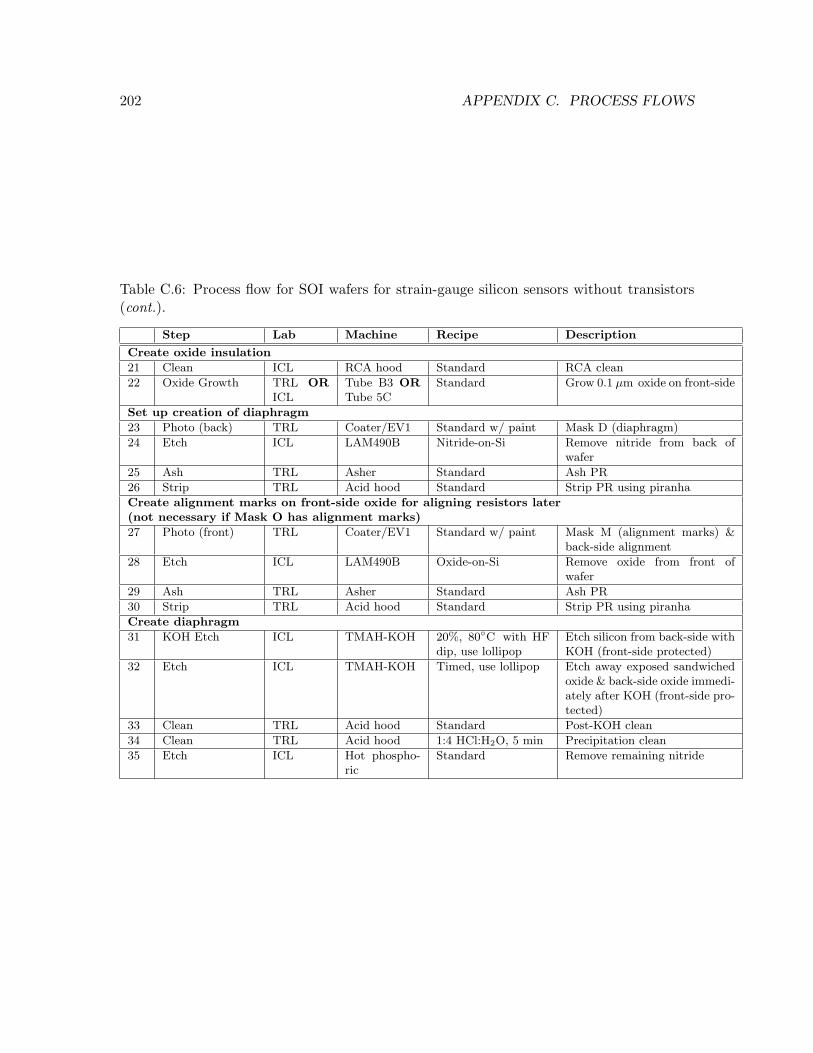
202 APPENDIX C. PROCESS FLOWS
Table C.6: Process flow for SOI wafers for strain-gauge silicon sensors without transistors(cont.).
Step Lab Machine Recipe Description
Create oxide insulation
21 Clean ICL RCA hood Standard RCA clean
22 Oxide Growth TRL ORICL
Tube B3 ORTube 5C
Standard Grow 0.1 µm oxide on front-side
Set up creation of diaphragm
23 Photo (back) TRL Coater/EV1 Standard w/ paint Mask D (diaphragm)
24 Etch ICL LAM490B Nitride-on-Si Remove nitride from back ofwafer
25 Ash TRL Asher Standard Ash PR
26 Strip TRL Acid hood Standard Strip PR using piranha
Create alignment marks on front-side oxide for aligning resistors later(not necessary if Mask O has alignment marks)
27 Photo (front) TRL Coater/EV1 Standard w/ paint Mask M (alignment marks) &back-side alignment
28 Etch ICL LAM490B Oxide-on-Si Remove oxide from front ofwafer
29 Ash TRL Asher Standard Ash PR
30 Strip TRL Acid hood Standard Strip PR using piranha
Create diaphragm
31 KOH Etch ICL TMAH-KOH 20%, 80C with HFdip, use lollipop
Etch silicon from back-side withKOH (front-side protected)
32 Etch ICL TMAH-KOH Timed, use lollipop Etch away exposed sandwichedoxide & back-side oxide immedi-ately after KOH (front-side pro-tected)
33 Clean TRL Acid hood Standard Post-KOH clean
34 Clean TRL Acid hood 1:4 HCl:H2O, 5 min Precipitation clean
35 Etch ICL Hot phospho-ric
Standard Remove remaining nitride

C.3. STRAIN-GAUGE SILICON SENSORS WITHOUT TRANSISTORS 203
Table C.7: Remainder of process flow for strain-gauge silicon sensors without transistors.
Step Lab Machine Recipe Description
Bond Pyrex and SOI wafers
36 Align TRL EV620 Standard Align the Pyrex and SOIwafers
37 Bond TRL EV501 Standard Bond the wafers
Create resistors
38 Clean TRL Acid hood Standard Clean wafers using piranha
39 Metal TRL E-beam Standard Evaporate 2000 A Cr then 100A Au on front
40 Photo (front) TRL Coater/EV1 Standard Mask R (resistors)
41 Etch TRL Acid hood Standard Etch front-side Au with goldetchant TFA or aqua regia
42 Etch TRL Acid hood Standard Etch front-side Cr with Cr-7
43 Ash TRL Asher Standard Ash PR
44 Strip TRL Acid hood Standard Strip PR using piranha
Add Parylene
45 Deposition TRL Parylene Standard Deposit Parylene
Test devices
46 Test — — — Test and measure devices

204 APPENDIX C. PROCESS FLOWS
C.4 Strain-Gauge Silicon Sensors With Transistors
Starting materials:
• 150 mm SOI wafers: Double-side polished (100) silicon with 20 µm n-type epi-layer
• 150 mm Pyrex wafers: Corning Pyrex 7740
The process flow is arranged into the following tables:
• Table C.8 describes the preparation of Pyrex for bonding with SOI.
• The sequence of Tables C.9, C.10 and C.11 describe transistor fabrication and partial
sensor fabrication on SOI wafers. They are independent of Table C.8.
• Table C.12 describes bonding of SOI with Pyrex and the remainder of the sensor
fabrication.

C.4. STRAIN-GAUGE SILICON SENSORS WITH TRANSISTORS 205
Table C.8: Process flow for Pyrex wafers for strain-gauge silicon sensors with transistors.
Step Lab Machine Recipe Description
1 Clean TRL Acid hood Standard Clean Pyrex wafers with 10min piranha and 15 s 50:1 HFdip
2 Clean TRL Asher Standard Clean wafers by ashing organics(optional)
3 Metal TRL E-beam Standard Evaporate 200 A Cr then 1000A Au on front-side
4 Clean TRL Acid hood Standard Clean wafers again with 10 minpiranha and 15 s 50:1 HF dip
5 Clean TRL Asher Standard Clean wafers again by ashing or-ganics (optional)
6 Metal TRL E-beam Standard Evaporate 200 A Cr then 1000A Au on back-side
7 Photo (front) TRL Coater/EV1 Standard (double-sided)
Mask P (Pyrex features) withback-side protection
8 Etch TRL Acid hood 28 A/s Etch Au with gold etchant TFAor aqua regia
9 Etch TRL Acid hood 25 A/s Etch Cr with Cr-7
10 Etch TRL Acid hood 0.8 µm/min Etch Pyrex with 660:140:200H2O:HNO3:HF
11 Strip TRL Acid hood Standard Strip PR
12 Strip TRL Acid hood 25 A/s Remove remaining Au with goldetchant TFA or aqua regia
13 Strip TRL Acid hood 28 A/s Remove remaining Cr with Cr-7
14 Storage TRL — — Save the Pyrex wafers for laterprocessing
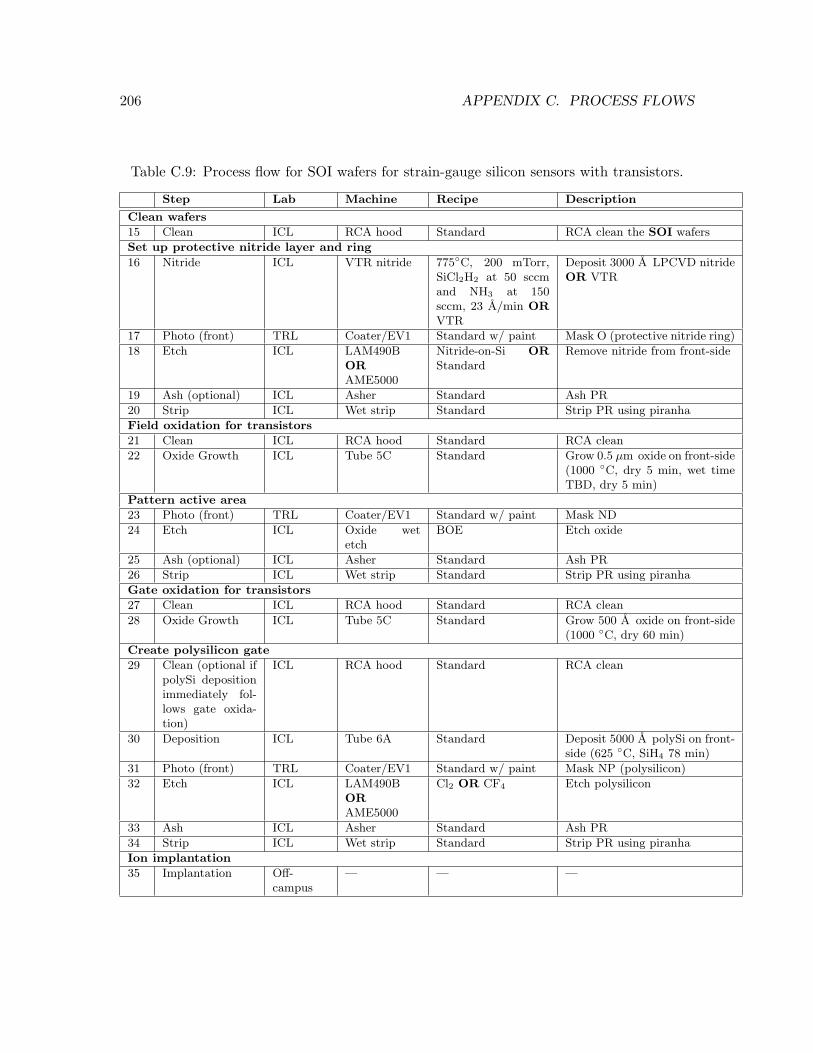
206 APPENDIX C. PROCESS FLOWS
Table C.9: Process flow for SOI wafers for strain-gauge silicon sensors with transistors.
Step Lab Machine Recipe Description
Clean wafers
15 Clean ICL RCA hood Standard RCA clean the SOI wafers
Set up protective nitride layer and ring
16 Nitride ICL VTR nitride 775C, 200 mTorr,SiCl2H2 at 50 sccmand NH3 at 150sccm, 23 A/min ORVTR
Deposit 3000 A LPCVD nitrideOR VTR
17 Photo (front) TRL Coater/EV1 Standard w/ paint Mask O (protective nitride ring)
18 Etch ICL LAM490BORAME5000
Nitride-on-Si ORStandard
Remove nitride from front-side
19 Ash (optional) ICL Asher Standard Ash PR
20 Strip ICL Wet strip Standard Strip PR using piranha
Field oxidation for transistors
21 Clean ICL RCA hood Standard RCA clean
22 Oxide Growth ICL Tube 5C Standard Grow 0.5 µm oxide on front-side(1000 C, dry 5 min, wet timeTBD, dry 5 min)
Pattern active area
23 Photo (front) TRL Coater/EV1 Standard w/ paint Mask ND
24 Etch ICL Oxide wetetch
BOE Etch oxide
25 Ash (optional) ICL Asher Standard Ash PR
26 Strip ICL Wet strip Standard Strip PR using piranha
Gate oxidation for transistors
27 Clean ICL RCA hood Standard RCA clean
28 Oxide Growth ICL Tube 5C Standard Grow 500 A oxide on front-side(1000 C, dry 60 min)
Create polysilicon gate
29 Clean (optional ifpolySi depositionimmediately fol-lows gate oxida-tion)
ICL RCA hood Standard RCA clean
30 Deposition ICL Tube 6A Standard Deposit 5000 A polySi on front-side (625 C, SiH4 78 min)
31 Photo (front) TRL Coater/EV1 Standard w/ paint Mask NP (polysilicon)
32 Etch ICL LAM490BORAME5000
Cl2 OR CF4 Etch polysilicon
33 Ash ICL Asher Standard Ash PR
34 Strip ICL Wet strip Standard Strip PR using piranha
Ion implantation
35 Implantation Off-campus
— — —

C.4. STRAIN-GAUGE SILICON SENSORS WITH TRANSISTORS 207
Table C.10: Process flow for SOI wafers for strain-gauge silicon sensors with transistors(cont.).
Step Lab Machine Recipe Description
Reoxidation/activation
36 Post-Ion ImplantClean
ICL Piranha / HF Standard Double piranha & HF dip
37 Clean ICL RCA hood Standard RCA clean
38 Oxide Growth ICL Tube 5B Standard Grow 500 A oxide on front-side(950 C, dry 15 min, wet 7 min,dry 15 min)
Pattern contact holes
39 Photo (front) TRL Coater/EV1 Standard w/ paint Mask NC
40 Etch TRL Acid hood 2 BOE Etch oxide
41 Ash (optional) ICL Asher Standard Ash PR
42 Strip ICL Wet strip Standard Strip PR using piranha
Add aluminum contacts
43 Clean ICL Pre-metal pi-ranha
Standard Pre-metal clean using piranha
44 Metal ICL Endura Standard Sputter 1 µm Al-1%Si on front
45 Photo (front) TRL Coater/EV1 Standard w/ paint Mask NM
46 Etch ICL PAN etch Standard PAN wet etch Al
47 Ash (optional) ICL Asher Standard Ash PR
48 Strip ICL Wet strip Standard Strip PR using Nano-StripTM
49 Sinter TRL Tube A3 Standard Sinter Al, 400C, 30 min N2/H2
Table C.11: Process flow for SOI wafers for strain-gauge silicon sensors with transistors(conc.).
Step Lab Machine Recipe Description
Set up creation of diaphragm
50 Photo (back) TRL Coater/EV1 Standard w/ paint Mask D (diaphragm)
51 Etch ICL LAM490B Nitride-on-Si Etch nitride from back of wafer(metal only on the side not be-ing etched)
52 Ash (optional) TRL Asher Standard Ash PR
53 Strip TRL Acid hood Standard Strip PR using Nano-StripTM(preferred over piranhadue to Al)
Create diaphragm
54 KOH Etch ICL TMAH-KOH 20%, 80C with HFdip, use red lollipop
Etch silicon from back-side withKOH (front-side protected)
55 Etch ICL TMAH-KOH Timed, use red lol-lipop
Etch away exposed sandwichedoxide & back-side oxide immedi-ately after KOH (front-side pro-tected)
56 Clean TRL Acid hood Standard Post-KOH clean with Nano-StripTM(preferred over piranhadue to Al)
57 Clean TRL Acid hood 1:4 HCl:H2O, 5 min Precipitation clean

208 APPENDIX C. PROCESS FLOWS
Table C.12: Remainder of process flow for strain-gauge silicon sensors with transistors.
Step Lab Machine Recipe Description
Bond Pyrex and SOI wafers
58 Clean TRL Acid hood Standard Clean wafers using Nano-StripTM(preferred over piranhadue to Al)
59 Align TRL EV620 Standard Align the Pyrex and SOIwafers
60 Bond TRL EV501 Standard Bond the wafers
Create resistors
61 Clean TRL Acid hood Standard Clean wafers using Nano-StripTM(preferred over piranhadue to Al)
62 Metal TRL E-beam Standard Evaporate 2000 A Cr then 100A Au on front
63 Photo (front) TRL Coater/EV1 Standard Mask R (resistors)
64 Etch TRL Acid hood 30–60 sec Etch Au with aqua regia (3:1HCl:HNO3)
65 Strip TRL Acid hood Standard Strip PR using Nano-StripTM(preferred over piranhadue to Al)
66 Etch TRL Acid hood Standard Etch Cr with Cr-7
Add Parylene
67 Deposition TRL Parylene Standard Deposit Parylene
Test devices
68 Test — — — Test and measure devices

Appendix D
Masks
This appendix contains the masks used in all rounds of fabrication. A description of the
design of these masks can be found in Section 3.8. Table D.1 lists the specific model in each
mask category for each round.
Mask Category
Round P N O M D R
1 D-1 D-2 — D-3 D-4 —
2 — — — — — D-5
3a D-1 D-2 — D-3 D-6 D-5
3b D-7 — D-8 — D-9 D-5
4 D-10 — D-11 — D-12 D-13
Table D.1: List of masks used for each round of devices. Each cell contains the figurenumber of the mask.
209
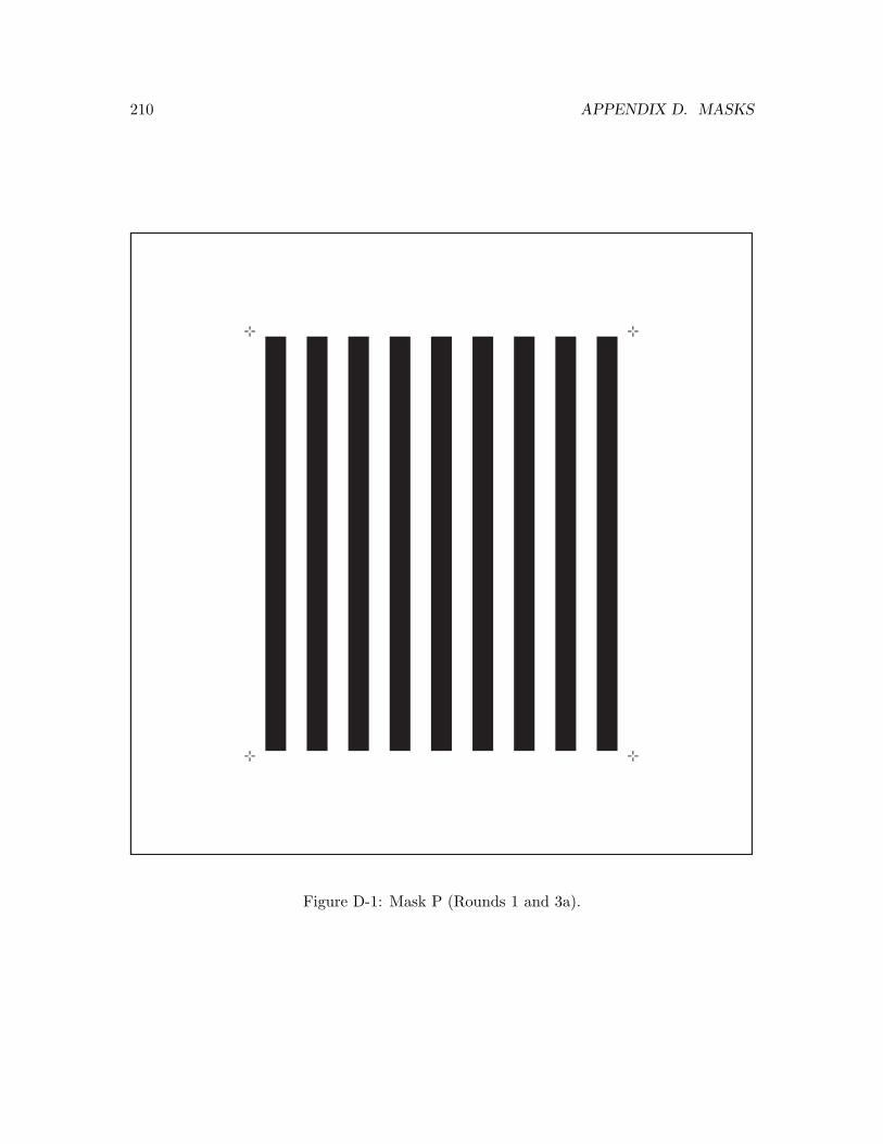
210 APPENDIX D. MASKS
Figure D-1: Mask P (Rounds 1 and 3a).
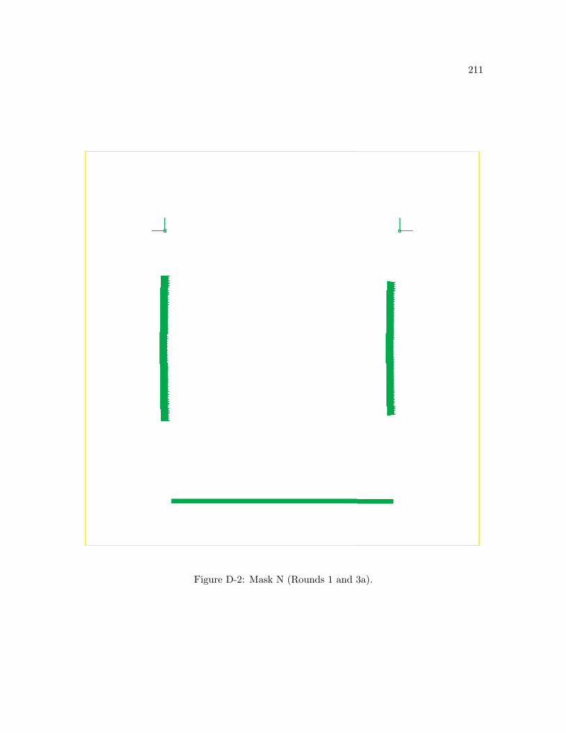
211
Figure D-2: Mask N (Rounds 1 and 3a).
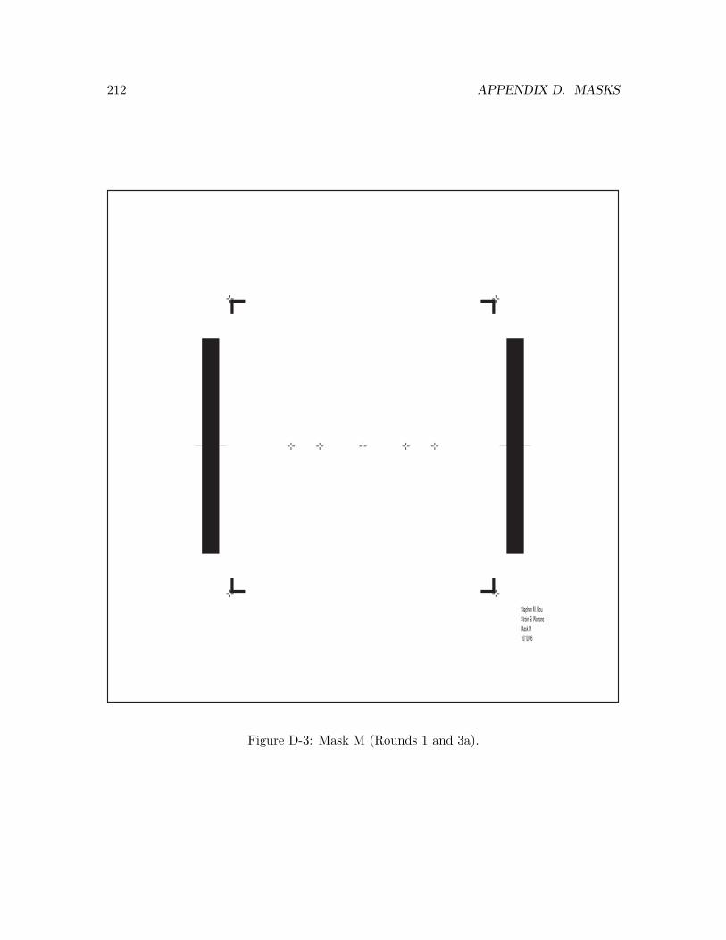
212 APPENDIX D. MASKS
Stephen M. Hou
Strain Si Wotrans
Mask M
10/10/06
Figure D-3: Mask M (Rounds 1 and 3a).
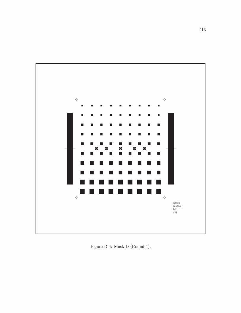
213
Stephen M. Hou
Strain Si Wotrans
Mask D
10/14/06
Figure D-4: Mask D (Round 1).
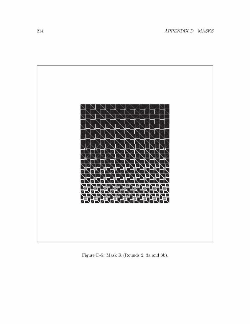
214 APPENDIX D. MASKS
Figure D-5: Mask R (Rounds 2, 3a and 3b).
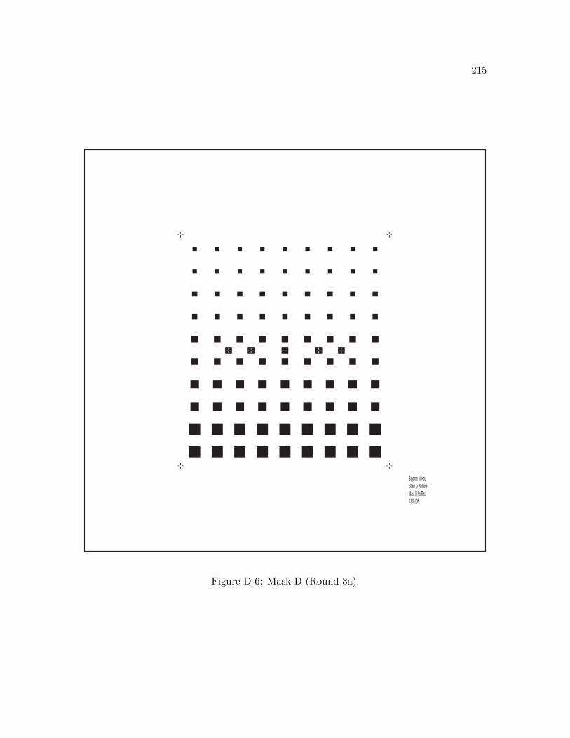
215
Stephen M. Hou
Strain Si Wotrans
Mask D No Rec
12/01//06
Figure D-6: Mask D (Round 3a).
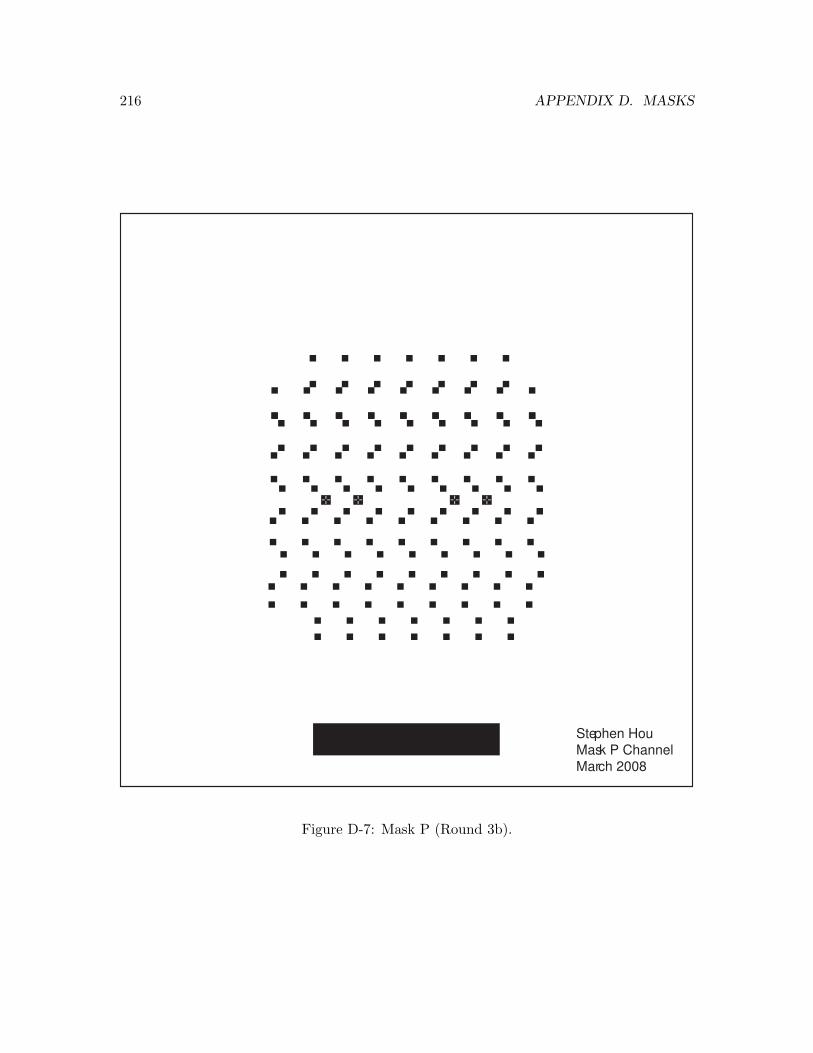
216 APPENDIX D. MASKS
Stephen Hou
Mask P Channel
March 2008
Figure D-7: Mask P (Round 3b).

217
Mask O
Stephen Hou
Mar 3, 2008
Figure D-8: Mask O (Round 3b).
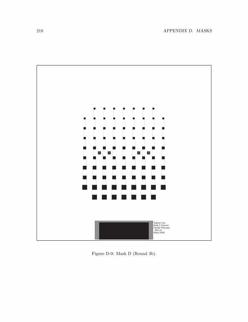
218 APPENDIX D. MASKS
Stephen HouMask D Channel Handle Thickness: 650 umMarch 2008
Figure D-9: Mask D (Round 3b).
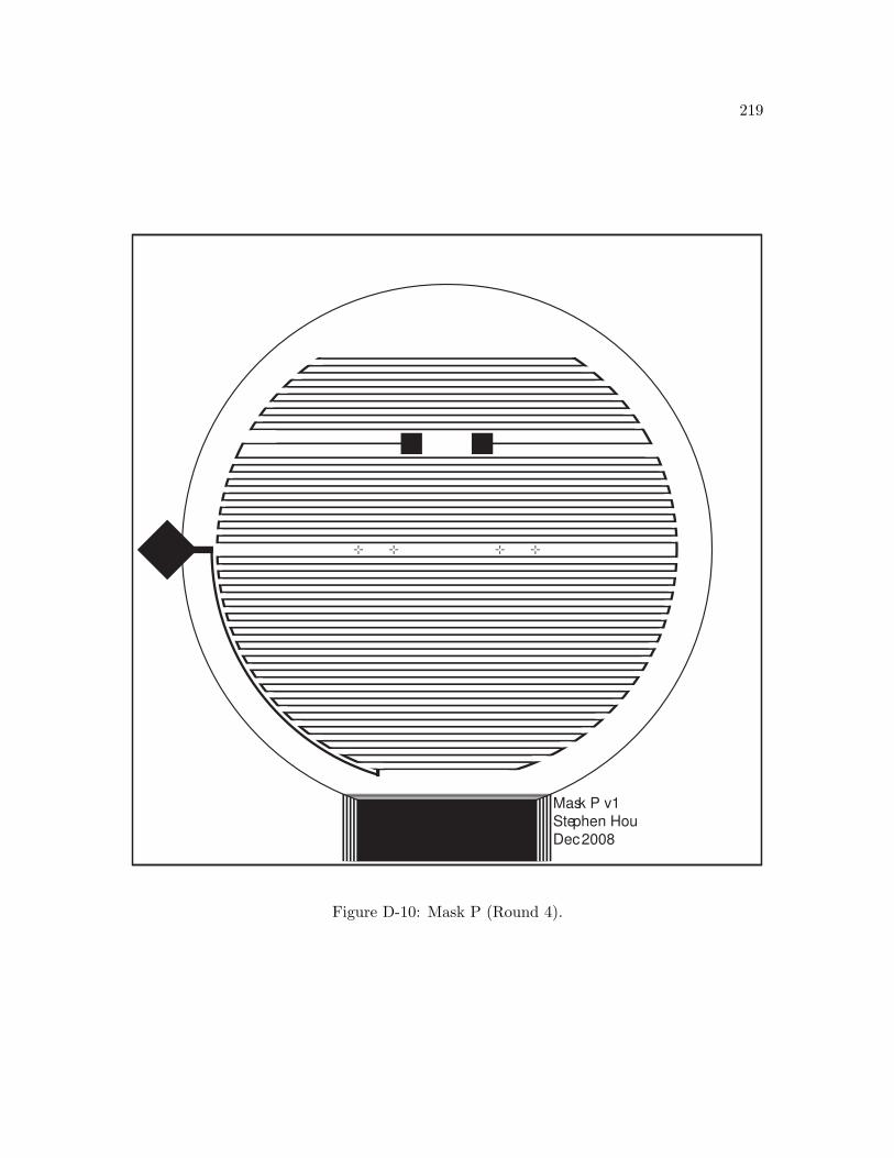
219
Mask P v1
Stephen Hou
Dec 2008
Figure D-10: Mask P (Round 4).
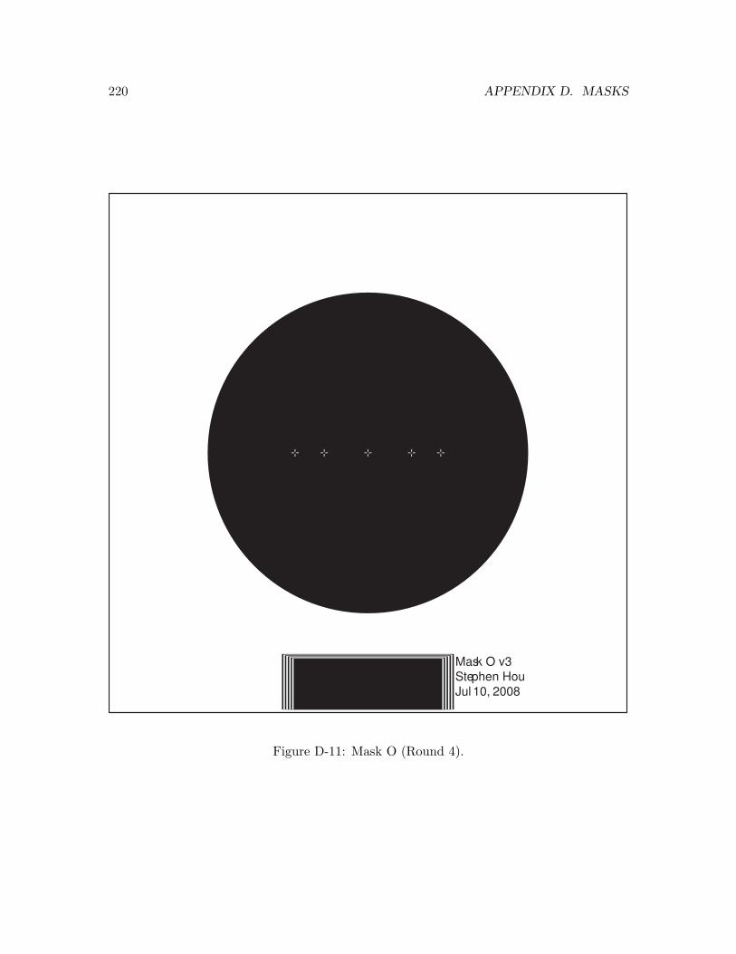
220 APPENDIX D. MASKS
Mask O v3
Stephen Hou
Jul 10, 2008
Figure D-11: Mask O (Round 4).
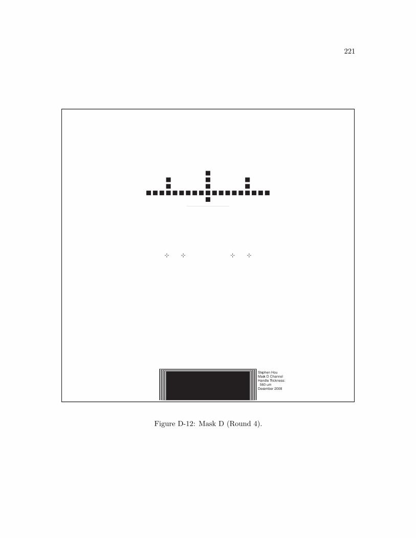
221
Stephen HouMask D Channel Handle Thickness: 560 umDecember 2008
Figure D-12: Mask D (Round 4).
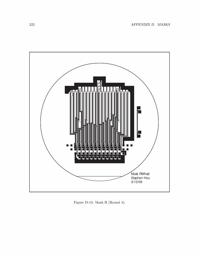
222 APPENDIX D. MASKS
Mask R Whe2
Stephen Hou
3/12/09
Figure D-13: Mask R (Round 4).

Appendix E
Apparatus
This appendix contains technical diagrams of the various apparatus used in fabrication and
measurement.
223
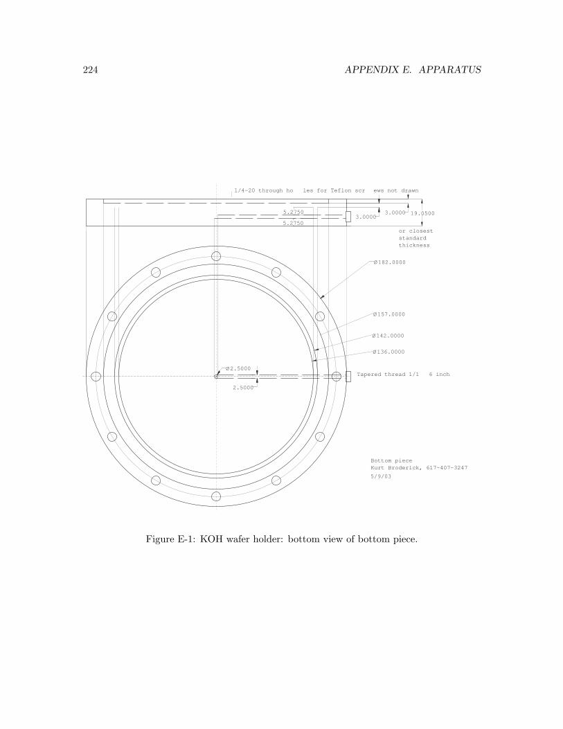
224 APPENDIX E. APPARATUS
Ø142.0000
Ø136.0000
Ø182.0000
Bottom piece
Kurt Broderick, 617-407-3247
Ø2.5000
3.0000
or closest
standard
thickness
1/4-20 through ho les for Teflon scr ews not drawn
3.0000
2.5000
Tapered thread 1/1 6 inch
19.05005.2750
5.2750
Ø157.0000
5/9/03
Figure E-1: KOH wafer holder: bottom view of bottom piece.
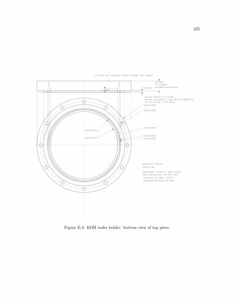
225
3.0000
19.0500
Ø142.0000
Ø136.0000
Ø130.0000 Ø139.0000
Ø168.0000
Ø182.0000
Top piece, bottom & side views
Kurt Broderick, 617-407-3247
[email protected], 5/9/03
Yellow region is O-ring
Please, provide O-ring, Buna-N DASH 253,
4.0000
or closest
standard thickness
Units: mm
1/4 inch 20 clearance Teflon screws (not drawn)
ID 136.12 mm, 3 mm thick
(ordered by Nuria de Mas)
Ø157.0000
Material: Teflon
Figure E-2: KOH wafer holder: bottom view of top piece.
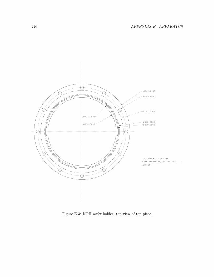
226 APPENDIX E. APPARATUS
Ø142.0000
Ø136.0000
Ø130.0000 Ø139.0000
Ø168.0000
Ø182.0000
Top piece, to p view
Kurt Broderick, 617-407-324 7
5/9/03
Ø157.0000
Figure E-3: KOH wafer holder: top view of top piece.
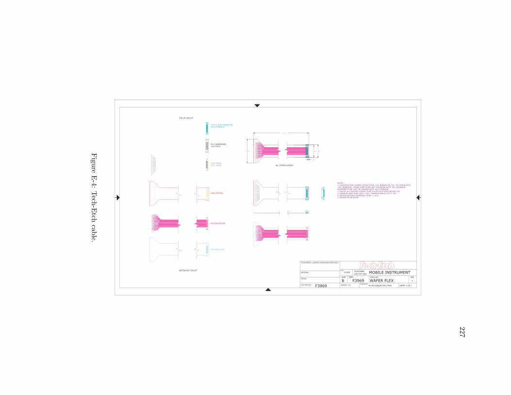
227
FR-4 HARDBOARD
.010 THICK
1
2
323
24
25
26
27
28
48
49
50
12
34
26
27
28
2956 30
31
3278
910 33
34
11
12
35
36
13
14
37
38
1516
39
40
17
18
41
42
1920
43
44
21
22
45
46
23
24
47
48
25
49
50
AND REF DOC
CUSTOMER
CAD FILE NO.:
TOLERANCES: (UNLESS OTHERWISE SPECIFIED)
FINISH:
MATERIAL:
B
SCALE: 1/1
SIZE
DATE
TEPN
SHEET 1 OF 1DRAWN BY
DWG NO. REV
ELLEN DORGAN-WILLMAN
3/2/09
NOTES:
1. CONSTRUCTION: COPPER LAYERS TO BE 1 OZ. BONDED TO .001" POLYIMIDE WITH
.001" ADHESIVE. COVER LAYER TO BE .001" POLYIMIDE WITH .001" ADHESIVE.
STIFFENER TO BE .032" FR-4 BOARD WITH .001" ADHESIVE.
2. FINISH: ALL EXPOSED COPPER TO BE PLATED WITH ELECTROLESS TIN.
3. MINIMUM LEAD TO BE .006+/-.001. MINIMUM SPACE .007+/-.001.
4. KAPTON OUTLINE TOLERANCE TO BE +/-.010.
5. SOLDER TO BE SN/PB.
12
325
50
26
25
50
126
227
24
49
BOTTOM COVER
BOTTOM COPPER
TOP COPPER
1 OZ. THICK
BASE KAPTON
TYCO D-SUB CONNECTOR
P/N: 5749069-5
TOP OF CIRCUIT
BOTTOM OF CIRCUIT
22.00
3.900 1.900 2.140
MOBILE INSTRUMENT
F3969 WAFER FLEX -
.020
F3969
ALL LAYERS SHOWN
Figu
reE-4:
Tech
-Etch
cable.

228 APPENDIX E. APPARATUS

Appendix F
MATLAB
This appendix contains the code for the MATLAB simulation, resistor design.m, used
to aid resistor design. The results of the simulation are discussed in Section 2.7.
229

230 APPENDIX F. MATLAB
%%%%%%%%%%%%%%%%%%%%%%%%%%%%%%%%%%%%%%%%%%%%%%%%%%%%%%%%%%%%
% %
% Displays the strain lines, optimal resistor direction, %
% and sign of resistor change %
% %
% resistor_design.m %
% %
%%%%%%%%%%%%%%%%%%%%%%%%%%%%%%%%%%%%%%%%%%%%%%%%%%%%%%%%%%%%
% material properties
nuR = 0.21; % Poisson’’s ratio (chromium resistor)
nuS = 0.0064; % Poisson’’s ratio (silicon diaphragm, <110> directions)
E = 169e9; % Young’’s modulus [Pa] (silicon diaphragm, <110> directions)
KE = 12*0.00133; % maximum deflection constant (silicon diaphragm, (100) plane)
% diaphragm dimensions
L = 2000e-6; % length [m]
H = 20e-6; % height [m]
% applied pressure
P = 1; % [Pa]
% strain constant (multiply this by normalized strain to get strain)
SC = -KE*(pi^2/2)*(1-nuS^2)*(L/H)^2*(P/E);
% x and y coordinates are normalized to be between -0.5 and +0.5
[x, y] = meshgrid(-0.5:0.005:0.5, -0.5:0.005:0.5);
% normalized strain nsx and nsy are the x- and y-dependent terms of
% the expression for strain
nsx = (cos(2*pi*x)).*(1 + cos(2*pi*y));
nsy = (cos(2*pi*y)).*(1 + cos(2*pi*x));
% compute the strains in both directions
sx = SC*nsx;
sy = SC*nsy;
close all;
% plot the x-strain; y-strain is inferred by symmetry
figure;
plot3(x, y, sx);
grid on;
xlabel(’Normalized x’);
ylabel(’Normalized y’);
zlabel(’\epsilon_x/P [Pa^-1]’);
% compute the local relative change in resistance when the
% resistor is placed lengthwise in the x and y directions

231
res_change_x = 1/(1-nuR)*sx + (2*nuR-1)/(1-nuR)*sy;
res_change_y = 1/(1-nuR)*sy + (2*nuR-1)/(1-nuR)*sx;
% show the local optimal lengthwise direction for resistor placement
figure;
for I = 1:size(x,1)
for J = 1:size(x,2)
if abs(res_change_x(I,J)) == abs(res_change_y(I,J)) % same
res_change_opt_dir_color(J,:,I) = [0,0,1]; % blue
elseif abs(res_change_x(I,J)) > abs(res_change_y(I,J)) % x better
res_change_opt_dir_color(J,:,I) = [0,1,0]; % green
else % y better
res_change_opt_dir_color(J,:,I) = [1,0,0]; % red
end
end
scatter(x(I,:), y(I,:), 4, res_change_opt_dir_color(:,:,I));
hold on;
end
xlabel(’Normalized x’);
ylabel(’Normalized y’);
axis square;
set(gca, ’XTick’, [-0.5:0.1:0.5]);
set(gca, ’YTick’, [-0.5:0.1:0.5]);
% show the sign of the resistance change when a local resistor
% is placed in the optimal direction
figure;
for I = 1:size(x,1)
for J = 1:size(x,2)
if max(abs(res_change_x(I,J)), abs(res_change_y(I,J))) == ...
max(res_change_x(I,J), res_change_y(I,J))
% the max absolute change is positive
res_change_opt_dir_sign_color(J,:,I) = [1,0,1]; % magenta
else % the max absolute is negative
res_change_opt_dir_sign_color(J,:,I) = [1,1,0]; % yellow
end
end
scatter(x(I,:), y(I,:), 4, res_change_opt_dir_sign_color(:,:,I));
hold on;
end
xlabel(’Normalized x’);
ylabel(’Normalized y’);
axis square;
set(gca, ’XTick’, [-0.5:0.1:0.5]);
set(gca, ’YTick’, [-0.5:0.1:0.5]);

232 APPENDIX F. MATLAB

Bibliography
[1] P.B. Adams. Bibliography on clean glass. Journal of Testing and Evaluation, 5(1):53–57, January 1977.
[2] Theodore Baumeister, Eugene A. Avallone, and Theodore Baumeister III. Marks’Standard Handbook for Mechanical Engineers. McGraw-Hill Book Company, New York,New York, eighth edition, 1978.
[3] Stephen Beeby, Graham Ensel, and Michael Kraft. MEMS Mechanical Sensors. ArtechHouse, Inc., Norwood, Massachusetts, 2004.
[4] A. Berns, U. Buder, E. Obermeier, A. Wolter, and A. Leder. AeroMEMS sensor arrayfor high-resolution wall pressure measurements. Sensors and Actuators A, 132(1):104–111, November 2006.
[5] D.C.S. Bien, P.V. Rainey, S.J.N. Mitchell, and H.S. Gamble. Characterization of mask-ing materials for deep glass micromachining. Journal of Micromechanics and Micro-engineering, 13:34–40, June 2003.
[6] T.Y. Bin and R.S. Huang. CAPSS: A thin diaphragm capacitive pressure sensor sim-ulator. Sensors and Actuators, 11(1):1–22, January 1987.
[7] G. Blasquez, Y. Naciri, P. Blondel, N. Ben Moussa, and P. Pons. Static response ofminiature capacitive pressure sensors with square or rectangular silicon diaphragm.Revue de Physique Appliquee, 22:505–510, July 1987.
[8] H. Bleckmann, I. Waldner, and E. Schwartz. Frequency discrimination of the surface-feeding fish Aplocheilus lineatus - a prerequisite for prey localization? Journal ofComparative Physiology A, 143:485–490, 1981.
[9] C. B. Braun and S. Coombs. The overlapping roles of the inner ear and lateral line:the active space of dipole source detection. Philosophical Transactions of the RoyalSociety of London, 355:1115–1119, 2000.
[10] Danick Briand, Patrick Weber, and Nicolaas F. de Rooij. Metal to glass anodic bondingfor microsystems packaging. In 12th International Conference on Solid State Sensors,Actuators and Microsystems, pages 1824–1827, Boston, Massachusetts, June 2003.
233
234 BIBLIOGRAPHY
[11] Danick Briand, Patrick Weber, and Nicolaas F. de Rooij. Integration of robust fluidicinterconnects using metal to glass anodic bonding. Journal of Micromechanics andMicroengineering, 15:1657–1663, July 2005.
[12] Colin A. Bulthaup, Eric J. Wilhelm, Brian N. Hubert, Brent A. Ridley, and Joseph M.Jacobson. All-additive fabrication of inorganic logic elements by liquid embossing.Applied Physics Letters, 79(10):1525–1527, September 2001.
[13] D.E. Campbell and P.B. Adams. Bibliography on clean glass: Supplement I. Journalof Testing and Evaluation, 14(5):260–265, September 1986.
[14] Stephen A. Campbell. The Science and Engineering of Microelectronic Fabrication.Oxford University Press, New York, New York, 1996.
[15] Abhijeet V. Chavan and Kensall D. Wise. Batch-processed vacuum-sealed capacitivepressure sensors. Journal of Microelectromechanical Systems, 10(4):580–588, December2001.
[16] Jack Chen, Jonathan Engel, Nannan Chen, Saunvit Pandya, Sheryl Coombs, andChang Liu. Artificial lateral line and hydrodynamic object tracking. In 19th IEEEInternational Conference on Micro Electro Mechanical Systems, Istanbul, Turkey, Jan-uary 2006.
[17] Nannan Chen, Jack Chen, Jonathan Engel, Saunvit Pandya, Craig Tucker, and ChangLiu. Development and characterization of high-sensitivity bioinspired artificial haircellsensor. In 12th Solid State Sensors, Actuator, and Microsystems Workshop, HiltonHead, South Carolina, June 2006.
[18] Eric Y. Chow, Brooke L. Beier, Antonio Francino, William J. Chappell, and Pedro P.Irazoqui. Toward an implantable wireless cardiac monitoring platform integratedwith an FDA-approved cardiovascular stent. Journal of Interventional Cardiology,22(5):479–487, 2009.
[19] Samuel K. Clark and Kensall D. Wise. Pressure sensitivity in anisotropically etchedthin-diaphragm pressure sensors. IEEE Transactions on Electron Devices, 26(12):1887–1896, December 1979.
[20] S. Coombs. Smart skins: Information processing by lateral line flow sensors. Au-tonomous Robotics, 11:255–261, 2001.
[21] S. Coombs and R. R. Fay. Dipole source localization by mottled sculpin, Cottus bairdi.Journal of the Acoustical Society of America, 93:2116–2123, 1993.
[22] S. Coombs, M. Hastings, and J. J. Finneran. Modeling and measuring lateral line exci-tation patterns to changing dipole source locations. Journal of Comparative PhysiologyA, 178:359–371, 1996.
BIBLIOGRAPHY 235
[23] Jason Dahl, Vicente Fernandez, Jeffrey Lang, Audrey Maertens, Michael Triantafyl-lou, and Frank Yaul. Lateral line-inspired sensor arrays for navigation and objectidentification. Marine Technology Society Journal, 45(4):130–146, July 2011.
[24] S. Dijkgraaf. The functioning and significance of the lateral-line organs. BiologicalReview, 38:51–105, April 1962.
[25] Zoran Djuric, Milan Matic, Jovan Matovi, Radomir Petrovic, and Nevenka Simicic.Experimental determination of silicon pressure sensor diaphragm deflection. Sensorsand Actuators A, 24:175–179, 1990.
[26] H.E. Elgamel. Closed-form expressions for the relationships between stress, diaphragmdeflection, and resistance change with pressure in silicon piezoresistive pressure sensors.Sensors and Actuators A: Physical, 50(1–2):17–22, August 1995.
[27] Jonathan Engel, Jack Chen, Nannan Chen, Saunvit Pandya, and Chang Liu. Devel-opment and characterization of an artificial hair cell based on polyurethane elastomerand force sensitive resistors. In 4th IEEE International Conference on Sensors, Irvine,California, October 2005.
[28] J. Englemann, W. Hanke, J. Mogdans, and H. Bleckmann. Hydrodynamic stimuli andthe fish lateral line. Nature, 408:51–52, November 2000.
[29] M. Esashi, S. Sugiyama, K. Ikeda, Y. Wang, and H. Miyashita. Vacuum-sealed siliconmicromachined pressure sensors. Proceedings of the IEEE, 86(8):1627–1639, Aug 1998.
[30] V.I. Fernandez, S.M. Hou, F.S. Hover, J.H. Lang, and M.S. Triantafyllou. Lateral-line-inspired MEMS-array pressure sensing for passive underwater navigation. In Proceed-ings of the International Symposium on Unmanned Untethered Submersible Technology(UUST), Lee, New Hampshire, August 2007.
[31] V.I. Fernandez, S.M. Hou, F.S. Hover, J.H. Lang, and M.S. Triantafyllou. Developmentand application of distributed MEMS pressure sensor array for AUV object avoidance.In Proceedings of the International Symposium on Unmanned Untethered SubmersibleTechnology (UUST), Lee, New Hampshire, August 2009.
[32] Vicente I. Fernandez. Performance Analysis for Lateral-Line-Inspired Sensor Arrays.PhD thesis, Massachusetts Institute of Technology, Cambridge, Massachusetts, 2011.
[33] Sawyer B. Fuller, Eric J. Wilhelm, and Joseph Jacobson. Ink-jet printed nanoparticlemicroelectromechanical systems. Journal of Microelectromechanical Systems, 11(1):54–60, February 2002.
[34] M. A. Gibbs. Lateral line receptors: Where do they come from developmentally andwhere is our research going? Brain, Behavior, and Evolution, 64:163–181, 2004.
[35] Bonnie L. Gray and Ronald S. Fearing. A surface micromachined microtactile sensorarray. In International Conference on Robotics and Automation, Minneapolis, Min-nesota, April 1996.
236 BIBLIOGRAPHY
[36] Briahna Gray. Artificial arrays could help submarines make like a fish. Science,313(5792):1382–1383, September 2006.
[37] G. G. Harris and W. A. van Bergeijk. Evidence that the lateral line organ respondsto near field displacements of sound sources in water. Journal of Acoustical Society ofAmerica, 34:1831–1841, 1962.
[38] E. S. Hassan. On the discrimination of spatial intervals by the blind cave fish (Anop-tichthys jordani). Journal of Comparative Physiology A, 159:701–710, 1986.
[39] El-S. Hassan. Mathematical analysis of the stimulus for the lateral line organ. BiologicalCybernetics, 52(1):23–36, May 1985.
[40] El-S. Hassan. Mathematical description of the stimuli to the lateral line system of fishderived from a three-dimensional flow field analysis I: The cases of moving in openwater and of gliding towards a plane surface. Biological Cybernetics, 66(5):443–452,March 1992.
[41] El-S. Hassan. Mathematical description of the stimuli to the lateral line system of fishderived from a three-dimensional flow field analysis II: The case of gliding alongside orabove a plane surface. Biological Cybernetics, 66(5):453–461, March 1992.
[42] El-S. Hassan. Mathematical description of the stimuli to the lateral line system offish derived from a three-dimensional flow field analysis III: The case of an oscillatingsphere near the fish. Biological Cybernetics, 69(6):525–538, October 1993.
[43] C. Hierold, B. Clasbrummel, D. Behrend, T. Scheiter, M. Steger, K. Oppermann,H. Kapels, E. Landgraf, D. Wenzel, and D. Etzrodt. Implantable low power integratedpressure sensor system for minimal invasive telemetric patient monitoring. In 11thAnnual International Workshop on Micro Electro Mechanical Systems, pages 568–573,Minneapolis, Minnesota, January 1998.
[44] Chih-Ming Ho and Yu-Chong Tai. Micro-electro-mechanical-systems (MEMS) and fluidflows. Annual Review of Fluid Mechanics, 30:579–612, January 1998.
[45] Matthew A. Hopcroft, William D. Nix, and Thomas W. Kenny. What is the Young’smodulus of silicon? Journal of Microelectromechanical Systems, 19(2):229–238, April2010.
[46] Stephen M. Hou. A piezo-tunable gigahertz cavity microelectromechanical resonator.Master’s thesis, Massachusetts Institute of Technology, Cambridge, Massachusetts,2004.
[47] Roger T. Howe and Charles G. Sodini. Microelectronics: An Integrated Approach.Prentice Hall, Upper Saddle River, New Jersey, 1997.
[48] Ciprian Iliescu, Bangtao Chen, and Jianmin Miao. On the wet etching of Pyrex glass.Sensors and Actuators A: Physical, 143(1):154–161, 2008.

BIBLIOGRAPHY 237
[49] Ciprian Iliescu, Francis E.H. Tay, and Jianmin Miao. Strategies in deep wet etching ofPyrex glass. Sensors and Actuators A: Physical, 133(2):395–400, 2007.
[50] Hyung-Kew Lee, Jaehoon Chung, Sun-Il Chang, and Euisik Yoon. Polymer tactilesensing array with a unit cell of multiple capacitors for three-axis contact force imageconstruction. In IEEE International Conference on Micro Electro Mechanical Systems,2007, pages 623–626, January 2007.
[51] Yong S. Lee and Kensall D. Wise. A batch-fabricated silicon capacitive pressuretransducer with low temperature sensitivity. IEEE Transactions on Electron Devices,29(1):42–48, January 1982.
[52] Jung Ah Lim, Wi Hyoung Lee, Hwa Sung Lee, Ji Hwang Lee, Yeong Don Park, andKilwon Cho. Self-organization of ink-jet-printed triisopropylsilylethynyl pentacene viaevaporation-induced flows in a drying droplet. Advanced Functional Materials, 18:229–234, January 2008.
[53] Chang Liu. Foundations of MEMS. Prentice Hall, Upper Saddle River, New Jersey,second edition, 2011.
[54] Yueh-Lin Loo, Takao Someya, Kirk W. Baldwin, Zhenan Bao, Peter Ho, Ananth Dod-abalapur, Howard E. Katz, and John A. Rogers. Soft, conformable electrical contactsfor organic semiconductors: High-resolution plastic circuits by lamination. Proceedingsof the National Academy of Sciences, 99(16):10252–10256, August 2002.
[55] Yueh-Lin Loo, Robert L. Willett, Kirk W. Baldwin, and John A. Rogers. Additive,nanoscale patterning of metal films with a stamp and a surface chemistry mediatedtransfer process: Applications in plastic electronics. Applied Physics Letters, 81(3):562–564, July 2002.
[56] Nadim Maluf. An Introduction to Microelectromechanical Systems Engineering. ArtechHouse, Inc., Norwood, Massachusetts, 2000.
[57] Stefan C. B. Mannsfeld, Benjamin C-K. Tee, Randall M. Stoltenberg, Christopher V.H-H. Chen, Soumendra Barman, Beinn V. O. Muir, Anatoliy N. Sokolov, Colin Reese,and Zhenan Bao. Highly sensitive flexible pressure sensors with microstructured rubberdielectric layers. In Nature Materials, pages 859–864, September 2010.
[58] J. Martin, W. Bacher, O.F. Hagena, and W.K. Schomburg. Strain gauge pressureand volume-flow transducers made by thermoplastic molding and membrane transfer.In 11th Annual International Workshop on Micro Electro Mechanical Systems, pages361–366, Jan 1998.
[59] John C. Montgomery, Sheryl Coombs, and Cindy F. Baker. The mechanosensorylateral line system of the hypogean form of Astyanax fasciatus. Environmental Biologyof Fishes, 62(1–3):87–96, October 2001.
238 BIBLIOGRAPHY
[60] Jithendra N. Palasagaram and Ramesh Ramadoss. MEMS-capacitive pressure sen-sor fabricated using printed-circuit-processing techniques. IEEE Sensors Journal,6(6):1374–1375, December 2006.
[61] Saunvit Pandya, Yingchen Yang, Douglas L. Jones, Jonathan Engel, and Chang Liu.Multisensor processing algorithms for underwater dipole localization and tracking usingMEMS artificial lateral-line sensors. EURASIP Journal on Applied Signal Processing,2006, 2006. Article ID 76593.
[62] Lalitha Parameswaran. Integrated Silicon Pressure Sensors Using Wafer Bonding Tech-nology. PhD thesis, Massachusetts Institute of Technology, Cambridge, Massachusetts,1997.
[63] S.B. Patil, V. Chu, and J.P. Conde. Performance of thin film silicon MEMS on flexibleplastic substrates. Sensors and Actuators A: Physical, 144(1):201–206, 2008.
[64] S. Paydavosi, F.M. Yaul, A.I. Wang, F. Niroui, T.L. Andrew, V. Bulovic, and J.H.Lang. MEMS switches employing active metal-polymer nanocomposites. In Proceedingsof the IEEE International Micro Electro Mechanical Systems Conference (MEMS),Paris, France, January 2012.
[65] Walter D. Pilkey. Formulas for Stress, Strain, and Structural Matrices. John Wiley &Sons, Inc., Hoboken, New Jersey, second edition, 2005.
[66] James D. Plummer, Michael D. Deal, and Peter B. Griffin. Silicon VLSI Technology:Fundamentals, Practice and Modeling. Prentice Hall, Inc., Upper Saddle River, NewJersey, 2000.
[67] K. Pohlmann, J. Atema, and T. Breithaupt. The importance of the lateral line innocturnal predation of piscivorous catfish. Journal of Experimental Biology, 207:2971–2978, 2004.
[68] Md Mosaddequr Rahman and Sazzadur Chowdhury. Square diaphragm CMUT ca-pacitance calculation using a new deflection shape function. Journal of Sensors, July2011.
[69] R. Rey, P. Charvet, M.T. Delaye, and S. Abou Hassan. A high density capacitivepressure sensor array for fingerprint sensor application. In 9th International Conferenceon Solid State Sensors and Actuators, pages 1453–1456, Chicago, Illinois, June 1997.
[70] Brent A. Ridley, Babak Nivi, and Joseph M. Jacobson. All-inorganic field effect tran-sistors fabricated by printing. Science, 286:746–749, October 1999.
[71] John A. Rogers, Zhenan Bao, Kirk Baldwin, Ananth Dodabalapur, Brian Crone, V.R.Raju, Valerie Kuck, Howard Katz, Karl Amundson, Jay Ewing, and Paul Drzaic.Paper-like electronic displays: Large-area rubber-stamped plastic sheets of electronicsand microencapsulated electrophoretic inks. Proceedings of the National Academy ofSciences, 98(9):4835–4840, April 2001.

BIBLIOGRAPHY 239
[72] Patrick Richard Scheeper, Børge Nordstrand, Jens Ole Gulløv, Bin Liu, ThomasClausen, Lise Midjord, and Torben Storgaard-Larsen. A new measurement microphonebased on MEMS technology. Journal of Microelectromechanical Systems, 12(6):880–891, December 2003.
[73] Stephen D. Senturia. Microsystem Design. Kluwer Academic Publishers, Boston,Massachusetts, 2001.
[74] Takao Someya, Yusaku Kato, Tsuyoshi Sekitani, Shingo Iba, Yoshiaki Noguchi,Yousuke Murase, Hiroshi Kawaguchi, and Takayasu Sakurai. Conformable, flexible,large-area networks of pressure and thermal sensors with organic transistor active ma-trixes. Proceedings of the National Academy of Sciences, 102(35):12321–12325, August2005.
[75] Takao Someya, Tsuyoshi Sekitani, Shingo Iba, Yusaku Kato, Hiroshi Kawaguchi, andTakayasu Sakurai. A large-area, flexible pressure sensor matrix with organic field-effect transistors for artificial skin applications. Proceedings of the National Academyof Sciences, 101(27):9966–9970, July 2004.
[76] S. Mark Spearing. MEMS materials and processes: A research overview. In Proceedingsof the Advanced Materials for Micro- and Nano-Systems (AMMNS) Programme of theSingapore-MIT Alliance Symposium, Singapore, Singapore, January 2003.
[77] G.A.C.M. Spierings. Wet chemical etching of silicate glasses in hydrofluoric acid basedsolutions. Journal of Materials Science, 28(23):6261–6273, December 1993.
[78] Susumu Sugiyama, Ken Kawahata, Masakazu Yoneda, and Isemi Igarashi. Tactileimage detection using a 1k-element silicon pressure sensor array. Sensors and ActuatorsA: Physical, 22(1–3):397–400, June 1989.
[79] Takao Suzuki and Tim Colonius. Inverse-imaging method for detection of vortex in achannel. American Institute of Aeronautics and Astronautics Journal, 41(9):1743–1751,September 2003.
[80] Francis H. Tay, Ciprian Iliescu, Ji Jing, and Jianmin Miao. Defect-free wet etchingthrough Pyrex glass using Cr/Au mask. Microsystem Technologies, 12(10–11):935–939, September 2006.
[81] T. Teyke. Collision with and avoidance of obstacles by blind cave fish Anoptichthysjordani (Characidae). Journal of Comparative Physiology A, 157:837–843, 1985.
[82] Stephen Timoshenko. Strength of Materials, Part I: Elementary Theory and Problems.Van Nostrand Reinhold Company, New York, New York, third edition, 1958.
[83] Stephen Timoshenko. Strength of Materials, Part II: Advanced Theory and Problems.Van Nostrand Reinhold Company, New York, New York, third edition, 1958.
240 BIBLIOGRAPHY
[84] Stephen Timoshenko. Theory of Plates and Shells. McGraw-Hill Book Company, Inc.,New York, New York, second edition, 1959.
[85] O.N. Tufte and D. Long. Recent developments in semiconductor piezoresistive devices.Solid-State Electronics, 6:323–338, 1963.
[86] S.M. van Netten. Hydrodynamic detection by cupulae in a lateral line canal: Functionalrelations between physics and physiology. Biological Cybernetics, 94:67–85, 2006.
[87] D. Vogel and H. Bleckmann. Behavioral discrimination of water motions caused bymoving objects. Journal of Comparative Physiology A, 186:1107–1117, 2000.
[88] Joel Voldman. A microfabricated liquid mixer for biomedical applications. Master’sthesis, Massachusetts Institute of Technology, Cambridge, Massachusetts, 1997.
[89] C. von Campenhausen, I. Riess, and R. Weissert. Detection of stationary objects by theblind cave fish Anoptichthys jordani (Characidae). Journal of Comparative Physiology,143:369–374, 1981.
[90] Xiaodong Wang, Baoqing Li, Onofrio L. Russo, Harry T. Roman, Ken K. Chin, andKenneth R. Farmer. Diaphragm design guidelines and an optical pressure sensor basedon MEMS technique. Microelectronics Journal, 37:50–56, 2006.
[91] R. Weissert and C. von Campenhausen. Discrimination between stationary objectsby the blind cave fish Anoptichthys jordani (Characidae). Journal of ComparativePhysiology A, 143:375–381, 1981.
[92] Kirt R. Williams, Kishan Gupta, and Matthew Wasilik. Etch rates for micromachin-ing processing – part II. Journal of Microelectromechanical Systems, 12(6):761–778,December 2003.
[93] Kirt R. Williams and Richard Muller. Etch rates for micromachining processing. Jour-nal of Microelectromechanical Systems, 5(4):256–269, December 1996.
[94] Y. Yang, J. Chen, J. Engel, S. Pandya, N. Chen, C. Tucker, S. Coombs, and C. Liu.Distant touch hydrodynamic imaging with an artificial lateral line. Proceedings of theNational Academy of Science, 103(50):18891–18895, December 2006.
[95] Yingchen Yang, Nannan Chen, Jonathan Engel, Craig Tucker, Saunvit Pandya, andChang Liu. From artificial haircell sensor to artificial lateral line system: Developmentand application. In 20th IEEE International Conference on Micro Electro MechanicalSystems, Kobe, Japan, January 2007.
[96] F.M. Yaul, V. Bulovic, and J.H. Lang. A flexible underwater pressure sensor arrayusing a conductive elastomer strain gauge. In Proceedings of the IEEE InternationalMicro Electro Mechanical Systems Conference (MEMS), Paris, France, January 2012.

BIBLIOGRAPHY 241
[97] Min-Xin Zhou, Qing-An Huang, Ming Qin, and Wei Zhou. A novel capacitive pres-sure sensor based on sandwich structures. Journal of Microelectromechanical Systems,14(6):1272–1282, December 2005.