Embedded benzocyclobutene in silicon: An integrated fabrication process for electrical and thermal...
14
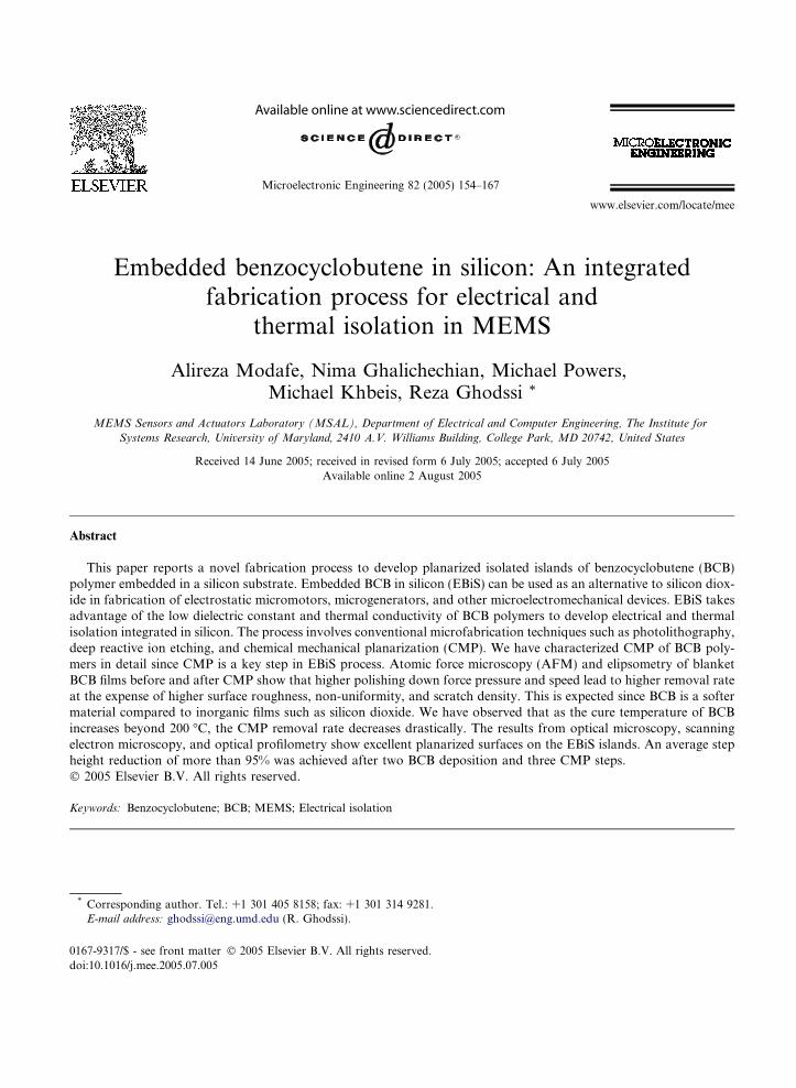
Embedded benzocyclobutene in silicon: An integrated fabrication process for electrical and thermal isolation in MEMS Alireza Modafe, Nima Ghalichechian, Michael Powers, Michael Khbeis, Reza Ghodssi * MEMS Sensors and Actuators Laboratory (MSAL), Department of Electrical and Computer Engineering, The Institute for Systems Research, University of Maryland, 2410 A.V. Williams Building, College Park, MD 20742, United States Received 14 June 2005; received in revised form 6 July 2005; accepted 6 July 2005 Available online 2 August 2005 Abstract This paper reports a novel fabrication process to develop planarized isolated islands of benzocyclobutene (BCB) polymer embedded in a silicon substrate. Embedded BCB in silicon (EBiS) can be used as an alternative to silicon diox- ide in fabrication of electrostatic micromotors, microgenerators, and other microelectromechanical devices. EBiS takes advantage of the low dielectric constant and thermal conductivity of BCB polymers to develop electrical and thermal isolation integrated in silicon. The process involves conventional microfabrication techniques such as photolithography, deep reactive ion etching, and chemical mechanical planarization (CMP). We have characterized CMP of BCB poly- mers in detail since CMP is a key step in EBiS process. Atomic force microscopy (AFM) and elipsometry of blanket BCB films before and after CMP show that higher polishing down force pressure and speed lead to higher removal rate at the expense of higher surface roughness, non-uniformity, and scratch density. This is expected since BCB is a softer material compared to inorganic films such as silicon dioxide. We have observed that as the cure temperature of BCB increases beyond 200 °C, the CMP removal rate decreases drastically. The results from optical microscopy, scanning electron microscopy, and optical profilometry show excellent planarized surfaces on the EBiS islands. An average step height reduction of more than 95% was achieved after two BCB deposition and three CMP steps. Ó 2005 Elsevier B.V. All rights reserved. Keywords: Benzocyclobutene; BCB; MEMS; Electrical isolation 0167-9317/$ - see front matter Ó 2005 Elsevier B.V. All rights reserved. doi:10.1016/j.mee.2005.07.005 * Corresponding author. Tel.: +1 301 405 8158; fax: +1 301 314 9281. E-mail address: [email protected] (R. Ghodssi). Microelectronic Engineering 82 (2005) 154–167 www.elsevier.com/locate/mee
-
Upload
washington -
Category
Documents
-
view
2 -
download
0
Transcript of Embedded benzocyclobutene in silicon: An integrated fabrication process for electrical and thermal...
Microelectronic Engineering 82 (2005) 154–167
www.elsevier.com/locate/mee
Embedded benzocyclobutene in silicon: An integratedfabrication process for electrical and
thermal isolation in MEMS
Alireza Modafe, Nima Ghalichechian, Michael Powers,Michael Khbeis, Reza Ghodssi *
MEMS Sensors and Actuators Laboratory (MSAL), Department of Electrical and Computer Engineering, The Institute for
Systems Research, University of Maryland, 2410 A.V. Williams Building, College Park, MD 20742, United States
Received 14 June 2005; received in revised form 6 July 2005; accepted 6 July 2005Available online 2 August 2005
Abstract
This paper reports a novel fabrication process to develop planarized isolated islands of benzocyclobutene (BCB)polymer embedded in a silicon substrate. Embedded BCB in silicon (EBiS) can be used as an alternative to silicon diox-ide in fabrication of electrostatic micromotors, microgenerators, and other microelectromechanical devices. EBiS takesadvantage of the low dielectric constant and thermal conductivity of BCB polymers to develop electrical and thermalisolation integrated in silicon. The process involves conventional microfabrication techniques such as photolithography,deep reactive ion etching, and chemical mechanical planarization (CMP). We have characterized CMP of BCB poly-mers in detail since CMP is a key step in EBiS process. Atomic force microscopy (AFM) and elipsometry of blanketBCB films before and after CMP show that higher polishing down force pressure and speed lead to higher removal rateat the expense of higher surface roughness, non-uniformity, and scratch density. This is expected since BCB is a softermaterial compared to inorganic films such as silicon dioxide. We have observed that as the cure temperature of BCBincreases beyond 200 �C, the CMP removal rate decreases drastically. The results from optical microscopy, scanningelectron microscopy, and optical profilometry show excellent planarized surfaces on the EBiS islands. An average stepheight reduction of more than 95% was achieved after two BCB deposition and three CMP steps.� 2005 Elsevier B.V. All rights reserved.
Keywords: Benzocyclobutene; BCB; MEMS; Electrical isolation
0167-9317/$ - see front matter � 2005 Elsevier B.V. All rights reserved.
doi:10.1016/j.mee.2005.07.005
* Corresponding author. Tel.: +1 301 405 8158; fax: +1 301 314 9281.E-mail address: [email protected] (R. Ghodssi).
A. Modafe et al. / Microelectronic Engineering 82 (2005) 154–167 155
1. Introduction
Electrical and thermal isolation, as well as phys-ical properties of dielectric materials, play anincreasingly important role in the performance,efficiency, and reliability of microelectromechani-cal systems (MEMS). The range of dielectric mate-rials and isolation techniques in MEMS hasgrown, especially in recent years. Traditionally, sil-icon dioxide has been and still is used for insula-tion in microelectronics and MEMS. Recentadvances in the area of power MEMS [1,2] includea significant number of research activities ondevelopment of crack-free, low-stress, and thicksilicon dioxide films [3–5]. In addition to electricalinsulation, thick silicon dioxide has been used forhigh-frequency [6] and thermal [7,8] isolation.The drawbacks of silicon dioxide as an insulatingfilm for MEMS applications include high dielectricconstant, limited thickness due to high residualstress, and high-temperature process, which affectsthe performance, efficiency, and reliability [9].
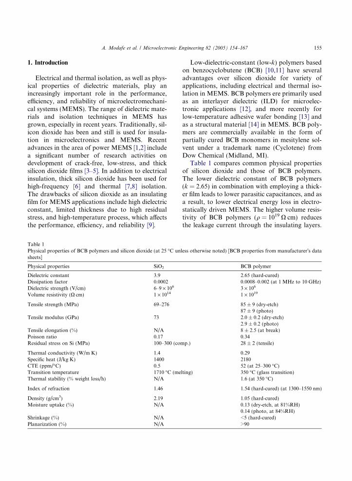
Table 1Physical properties of BCB polymers and silicon dioxide (at 25 �C unsheets]
Physical properties SiO2
Dielectric constant 3.9Dissipation factor 0.0002Dielectric strength (V/cm) 6–9 · 106
Volume resistivity (X cm) 1 · 1014
Tensile strength (MPa) 69–276
Tensile modulus (GPa) 73
Tensile elongation (%) N/APoisson ratio 0.17Residual stress on Si (MPa) 100–300 (com
Thermal conductivity (W/m K) 1.4Specific heat (J/kg K) 1400CTE (ppm/�C) 0.5Transition temperature 1710 �C (meThermal stability (% weight loss/h) N/A
Index of refraction 1.46
Density (g/cm3) 2.19Moisture uptake (%) N/A
Shrinkage (%) N/APlanarization (%) N/A
Low-dielectric-constant (low-k) polymers basedon benzocyclobutene (BCB) [10,11] have severaladvantages over silicon dioxide for variety ofapplications, including electrical and thermal iso-lation in MEMS. BCB polymers ere primarily usedas an interlayer dielectric (ILD) for microelec-tronic applications [12], and more recently forlow-temperature adhesive wafer bonding [13] andas a structural material [14] in MEMS. BCB poly-mers are commercially available in the form ofpartially cured BCB monomers in mesitylene sol-vent under a trademark name (Cyclotene) fromDow Chemical (Midland, MI).
Table 1 compares common physical propertiesof silicon dioxide and those of BCB polymers.The lower dielectric constant of BCB polymers(k = 2.65) in combination with employing a thick-er film leads to lower parasitic capacitances, and asa result, to lower electrical energy loss in electro-statically driven MEMS. The higher volume resis-tivity of BCB polymers (q = 1019 X cm) reducesthe leakage current through the insulating layers.
less otherwise noted) [BCB properties from manufacturer�s data
BCB polymer
2.65 (hard-cured)0.0008–0.002 (at 1 MHz to 10 GHz)3 · 106
1 · 1019
85 ± 9 (dry-etch)87 ± 9 (photo)2.0 ± 0.2 (dry-etch)2.9 ± 0.2 (photo)8 ± 2.5 (at break)0.34
p.) 28 ± 2 (tensile)
0.29218052 (at 25–300 �C)
lting) 350 �C (glass transition)1.6 (at 350 �C)
1.54 (hard-cured) (at 1300–1550 nm)
1.05 (hard-cured)0.13 (dry-etch, at 81%RH)0.14 (photo, at 84%RH)<5 (hard-cured)>90
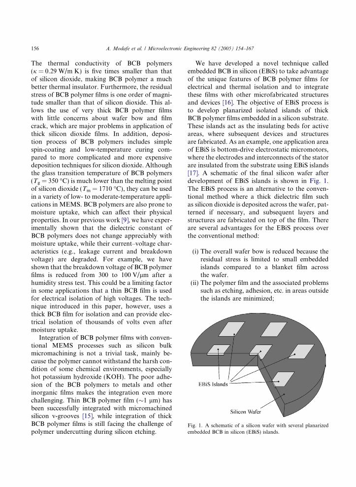
Fig. 1. A schematic of a silicon wafer with several planarizedembedded BCB in silicon (EBiS) islands.
156 A. Modafe et al. / Microelectronic Engineering 82 (2005) 154–167
The thermal conductivity of BCB polymers(j = 0.29 W/m K) is five times smaller than thatof silicon dioxide, making BCB polymer a muchbetter thermal insulator. Furthermore, the residualstress of BCB polymer films is one order of magni-tude smaller than that of silicon dioxide. This al-lows the use of very thick BCB polymer filmswith little concerns about wafer bow and filmcrack, which are major problems in application ofthick silicon dioxide films. In addition, deposi-tion process of BCB polymers includes simplespin-coating and low-temperature curing com-pared to more complicated and more expensivedeposition techniques for silicon dioxide. Althoughthe glass transition temperature of BCB polymers(Tg = 350 �C) is much lower than the melting pointof silicon dioxide (Tm = 1710 �C), they can be usedin a variety of low- to moderate-temperature appli-cations in MEMS. BCB polymers are also prone tomoisture uptake, which can affect their physicalproperties. In our previous work [9], we have exper-imentally shown that the dielectric constant ofBCB polymers does not change appreciably withmoisture uptake, while their current–voltage char-acteristics (e.g., leakage current and breakdownvoltage) are degraded. For example, we haveshown that the breakdown voltage of BCB polymerfilms is reduced from 300 to 100 V/lm after ahumidity stress test. This could be a limiting factorin some applications that a thin BCB film is usedfor electrical isolation of high voltages. The tech-nique introduced in this paper, however, uses athick BCB film for isolation and can provide elec-trical isolation of thousands of volts even aftermoisture uptake.
Integration of BCB polymer films with conven-tional MEMS processes such as silicon bulkmicromachining is not a trivial task, mainly be-cause the polymer cannot withstand the harsh con-dition of some chemical environments, especiallyhot potassium hydroxide (KOH). The poor adhe-sion of the BCB polymers to metals and otherinorganic films makes the integration even morechallenging. Thin BCB polymer film (�1 lm) hasbeen successfully integrated with micromachinedsilicon v-grooves [15], while integration of thickBCB polymer films is still facing the challenge ofpolymer undercutting during silicon etching.
We have developed a novel technique calledembedded BCB in silicon (EBiS) to take advantageof the unique features of BCB polymer films forelectrical and thermal isolation and to integratethese films with other microfabricated structuresand devices [16]. The objective of EBiS process isto develop planarized isolated islands of thickBCB polymer films embedded in a silicon substrate.These islands act as the insulating beds for activeareas, where subsequent devices and structuresare fabricated. As an example, one application areaof EBiS is bottom-drive electrostatic micromotors,where the electrodes and interconnects of the statorare insulated from the substrate using EBiS islands[17]. A schematic of the final silicon wafer afterdevelopment of EBiS islands is shown in Fig. 1.The EBiS process is an alternative to the conven-tional method where a thick dielectric film suchas silicon dioxide is deposited across the wafer, pat-terned if necessary, and subsequent layers andstructures are fabricated on top of the film. Thereare several advantages for the EBiS process overthe conventional method:
(i) The overall wafer bow is reduced because theresidual stress is limited to small embeddedislands compared to a blanket film acrossthe wafer.
(ii) The polymer film and the associated problemssuch as etching, adhesion, etc. in areas outsidethe islands are minimized;
Table 2CMP control and output parameters
Control parameter Output parameter
Down force pressure RRa, RUb, RSc
Wafer carrier rotation speed RR, RU, RS
A. Modafe et al. / Microelectronic Engineering 82 (2005) 154–167 157
(iii) The subsequent fabrication processes are lessprone to fabrication defects, leading to higheryields because the islands are highlyplanarized.
(iv) Since the polymer layer is embedded in thesubstrate, the adhesion of the polymer to thesubstrate is improved compared to blanketfilm.
(v) The overall adhesion of the metal films to thesubstrate is improved by limiting the polymerto a small area on the substrate.
(iv) In case of etching silicon v-grooves in hotKOH, the polymer can be completely maskedwith a metal layer to prevent undercut.
The EBiS process is adopted from thick buriedoxide in silicon (TBOS) process [3]. TBOS is a fab-rication process developed to create isolated is-lands of plasma-enhanced chemical vapordeposited (PECVD) silicon dioxide to reduce theoverall wafer bow for subsequent wafer bonding.EBiS, however, enables the incorporation ofspin-on, thick BCB polymer films in silicon sub-strate, leading to excellent electrical and thermalisolation, lower electrical energy loss, lower resid-ual stress and wafer bow, and easier fabricationand process integration.
This paper introduces the EBiS process as anenabling tool for electrical and thermal isolationin fabrication of MEMS. Since chemical mechani-cal planarization (CMP) of BCB polymers is a keyprocess step in EBiS, Sections 2 and 3 review theCMP process, its parameters, the specifics of thisstudy, and presents the characterization resultsfor CMP of blanket BCB polymer films. In Section4, we will go over the EBiS fabrication process,present fabrication results, and discuss measure-ment data. Finally, Section 5 provides concludingremarks.
Platen rotation speed RR, RU, RSSlurry chemistry RR, RS, STd
Slurry abrasive (type, size, percent) RR, RS, STPad hardness RR, RU, RS, STPad porosity RUWafer carrier film hardness RU
a RR, removal rate.b RU, removal uniformity.c RS, removal selectivity.d ST, surface topography.
2. Planarization of BCB polymers
The surface of the wafer is globally planarizedduring the EBiS process, although BCB polymersare excellent planarizers with a degree of planari-zation (DOP) of about 95% when coated over iso-
lated, shallow trenches [12]. The planarization ofBCB polymers in EBiS process is achieved usingCMP, which is the de facto standard for globalplanarization in integrated circuit chip fabricationtoday [18].
CMP is a planarization method that uses acombination of mechanical abrasion and chemicaletching to physically remove material from placesof high topography and flatten the wafer surface.In all experiments presented in this paper, a 6ECCMP tool from Strasbaugh (San Luis Obispo,CA) was used for polishing the wafers.
The output parameters that are commonly usedto benchmark a CMP process are removal rate, re-moval uniformity, removal selectivity, and surfacetopography of the polished film. These parametersare the result of mechanical and chemical interac-tion at the interface of three major components ofa CMP process: polishing pad, polishing slurry,and wafer. There are several variables that affectthese interactions and control the output parame-ters, making the CMP process a complicatedphenomenon to analyze and model. Table 2 sum-marizes some of the control parameters and theaffected output parameters in a generic CMP pro-cess [19].
The control parameters of CMP are not limitedto those listed in Table 2. For instance, the param-eters of pad conditioning can greatly impact thepolishing results. Some CMP tools (including6EC) allow the user to apply a back pressure (po-sitive or negative) on the wafer to compensate for
158 A. Modafe et al. / Microelectronic Engineering 82 (2005) 154–167
the wafer bow or apply a pressure to the retainingring to adjust the polish of the wafer edge. Platentemperature, slurry flow rate, and polishing timealso affect the output parameters. The most impor-tant control parameters are down force pressure,platen rotation speed, and wafer carrier rotationspeed. These parameters determine the removalrate of the film based on the empirical Prestonequation [20]
RR ¼ KpPV ; ð1Þwhere RR is the removal rate, V is the linear veloc-ity of the platen relative to the wafer, P is the downforce pressure pressing the wafer onto the pad, andKp is the Preston coefficient. The Preston coeffi-cient is a function of the mechanical and chemicalproperties of the polishing pad, slurry, and the filmbeing polished. Considering only the mechanicalproperties of the film, it has been shown that thePreston coefficient is inversely proportional tothe Young�s modulus of the film [21]
Kp ¼1
2E; ð2Þ
where E is the Young�s modulus of the film beingpolished. It has also been shown that (1) mostlyapplies to hard-pad CMP systems while RR is pro-portional to P1.5 instead of P for soft-pad CMPsystems [22]. More complete and accurate CMPmodels can be found in the literature [23–29].
CMP of polymer materials such as BCB poly-mers is more challenging than inorganic materialssuch as silicon dioxide and metals. Some specificproperties of BCB polymers result in observationof distinct phenomena during CMP process: (i)BCB polymers are known to have hydrophobicsurfaces [30], resulting in low surface reactivityand low removal rate; (ii) the hardness of the poly-mers is lower than that of inorganic materials,leading to high levels of scratching and post-CMP defects; (iii) the low hardness of the poly-mers can also result in embedded abrasive particlesin the polished film and (iv) the level of polymercross-linking is a function of cure temperatureand time. Therefore, the hardness and surfacereactivity of BCB polymers, and as a result theirremoval rate, strongly depend on cure temperatureand time.
3. Characterization of CMP for BCB polymers
Considering the challenges in planarization ofBCB polymers, it is important to understand thebehavior of blanket BCB polymer films in CMPprocess before characterizing the CMP processfor more complicated structures such as EBiS is-lands. Furthermore, such characterization canhelp with the design and optimization of the EBiSprocess. For these reasons, we conducted a seriesof experiments to study and characterize theCMP process for BCB polymers. In this character-ization, we were mainly interested in the differencebetween parameters of uncured and cured films,such as removal rate, non-uniformity, and surfacetopography.
The physical properties of dry-etch and photo-sensitive BCB polymers, as Table 1 shows, haveminor differences. Therefore, the characterizationsamples were prepared with the dry-etch (non-photosensitive) BCB polymer (Cyclotene 3022-63) instead of the photosensitive BCB polymer(Cyclotene 4026-46), which is used in the EBiSprocess. All samples were 400 silicon wafers andprepared in the following manner. Each waferwas dehydrated at 130 �C for 10 min on a hotplate.AP3000, an adhesion promoter developed forCyclotene by Dow Chemical, was dispensed andspun onto the wafer at 3000 rpm for 30 s. Next,Cyclotene 3022-63 was dispensed and spun ontothe wafer, first at 500 rpm for 8 s and then, at5000 rpm for 30 s. The sample was then baked at85 �C for 150 s on hotplate. This was only doneto drive out the remaining solvent. Several waferswere prepared and cured at different temperaturesto study the effect of cure temperature on CMPparameters.
All wafers in this study were polished in our6EC CMP tool with a k-grooved IC-1000 padstacked on a SUBA IV pad from Rohm and HaasElectronic Materials (Phoenix, AZ). The specifica-tions of the slurries used in this research,MSW2000A from Rohm and Haas ElectronicMaterials and ILD1300 from Nitta Haas Incorpo-rated (Osaka, Japan), are listed in Table 3. Table 4shows the polishing and pad conditioning param-eters of the two CMP recipes that we used for pol-ishing wafers.
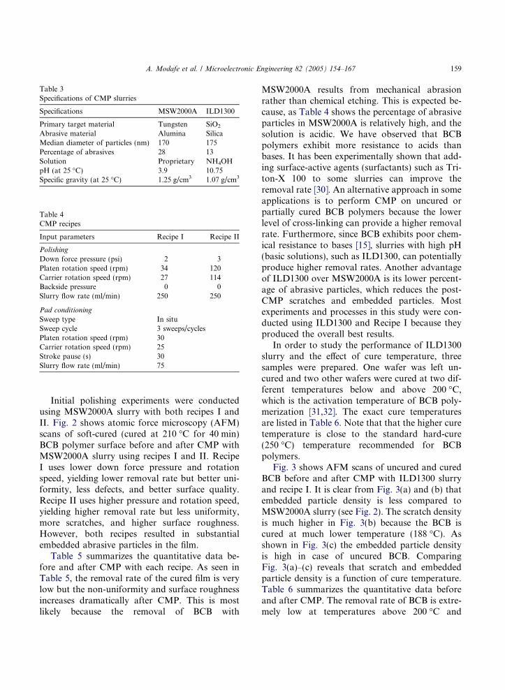
Table 3Specifications of CMP slurries
Specifications MSW2000A ILD1300
Primary target material Tungsten SiO2
Abrasive material Alumina SilicaMedian diameter of particles (nm) 170 175Percentage of abrasives 28 13Solution Proprietary NH4OHpH (at 25 �C) 3.9 10.75Specific gravity (at 25 �C) 1.25 g/cm3 1.07 g/cm3
Table 4CMP recipes
Input parameters Recipe I Recipe II
Polishing
Down force pressure (psi) 2 3Platen rotation speed (rpm) 34 120Carrier rotation speed (rpm) 27 114Backside pressure 0 0Slurry flow rate (ml/min) 250 250
Pad conditioning
Sweep type In situSweep cycle 3 sweeps/cyclesPlaten rotation speed (rpm) 30Carrier rotation speed (rpm) 25Stroke pause (s) 30Slurry flow rate (ml/min) 75
A. Modafe et al. / Microelectronic Engineering 82 (2005) 154–167 159
Initial polishing experiments were conductedusing MSW2000A slurry with both recipes I andII. Fig. 2 shows atomic force microscopy (AFM)scans of soft-cured (cured at 210 �C for 40 min)BCB polymer surface before and after CMP withMSW2000A slurry using recipes I and II. RecipeI uses lower down force pressure and rotationspeed, yielding lower removal rate but better uni-formity, less defects, and better surface quality.Recipe II uses higher pressure and rotation speed,yielding higher removal rate but less uniformity,more scratches, and higher surface roughness.However, both recipes resulted in substantialembedded abrasive particles in the film.
Table 5 summarizes the quantitative data be-fore and after CMP with each recipe. As seen inTable 5, the removal rate of the cured film is verylow but the non-uniformity and surface roughnessincreases dramatically after CMP. This is mostlikely because the removal of BCB with
MSW2000A results from mechanical abrasionrather than chemical etching. This is expected be-cause, as Table 4 shows the percentage of abrasiveparticles in MSW2000A is relatively high, and thesolution is acidic. We have observed that BCBpolymers exhibit more resistance to acids thanbases. It has been experimentally shown that add-ing surface-active agents (surfactants) such as Tri-ton-X 100 to some slurries can improve theremoval rate [30]. An alternative approach in someapplications is to perform CMP on uncured orpartially cured BCB polymers because the lowerlevel of cross-linking can provide a higher removalrate. Furthermore, since BCB exhibits poor chem-ical resistance to bases [15], slurries with high pH(basic solutions), such as ILD1300, can potentiallyproduce higher removal rates. Another advantageof ILD1300 over MSW2000A is its lower percent-age of abrasive particles, which reduces the post-CMP scratches and embedded particles. Mostexperiments and processes in this study were con-ducted using ILD1300 and Recipe I because theyproduced the overall best results.
In order to study the performance of ILD1300slurry and the effect of cure temperature, threesamples were prepared. One wafer was left un-cured and two other wafers were cured at two dif-ferent temperatures below and above 200 �C,which is the activation temperature of BCB poly-merization [31,32]. The exact cure temperaturesare listed in Table 6. Note that that the higher curetemperature is close to the standard hard-cure(250 �C) temperature recommended for BCBpolymers.
Fig. 3 shows AFM scans of uncured and curedBCB before and after CMP with ILD1300 slurryand recipe I. It is clear from Fig. 3(a) and (b) thatembedded particle density is less compared toMSW2000A slurry (see Fig. 2). The scratch densityis much higher in Fig. 3(b) because the BCB iscured at much lower temperature (188 �C). Asshown in Fig. 3(c) the embedded particle densityis high in case of uncured BCB. ComparingFig. 3(a)–(c) reveals that scratch and embeddedparticle density is a function of cure temperature.Table 6 summarizes the quantitative data beforeand after CMP. The removal rate of BCB is extre-mely low at temperatures above 200 �C and

Fig. 2. AFM scans of BCB polymer surface cured at 210 �C showing the effect of CMP with MSW2000A slurry: (a) before CMP; (b)after CMP with recipe I; (c) after CMP with recipe II.
Table 5Specifications of soft-cured BCB film before and after CMPwith MSW2000A slurry and recipes I and II
Parameters Pre-CMP Recipe I Recipe II
Polishing time (s) N/A 120 120Non-uniformity (%) 0.3 0.8 1.8Removal rate (nm/min) N/A 7 45
P–P roughness (A) 41 1383 1511Mean roughness (A) 4 7 12RMS roughness (A) 5 29 33
160 A. Modafe et al. / Microelectronic Engineering 82 (2005) 154–167
increases as the cure temperature decreases below200 �C. The removal rate is quite high for uncuredBCB. The surface roughness of the film decreasesafter CMP for cure temperatures above 200 �Cwhile it increases as the cure temperature goes be-low 200 �C. This shows that the CMP characteris-tics of BCB film are determined by the curetemperature, so that by controlling the level ofpolymerization through cure temperature, the out-put parameters of CMP process can be adjusted.
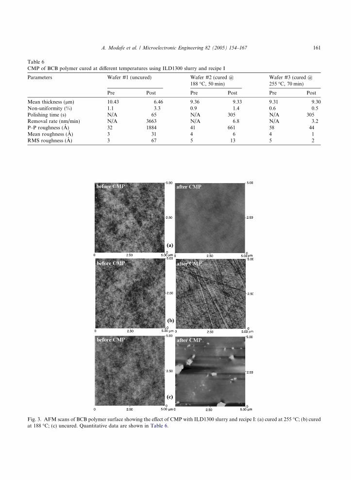
Table 6CMP of BCB polymer cured at different temperatures using ILD1300 slurry and recipe I
Parameters Wafer #1 (uncured) Wafer #2 (cured @188 �C, 50 min)
Wafer #3 (cured @255 �C, 70 min)
Pre Post Pre Post Pre Post
Mean thickness (lm) 10.43 6.46 9.36 9.33 9.31 9.30Non-uniformity (%) 1.1 3.3 0.9 1.4 0.6 0.5Polishing time (s) N/A 65 N/A 305 N/A 305Removal rate (nm/min) N/A 3663 N/A 6.8 N/A 3.2P–P roughness (A) 32 1884 41 661 58 44Mean roughness (A) 3 31 4 6 4 1RMS roughness (A) 3 67 5 13 5 2
Fig. 3. AFM scans of BCB polymer surface showing the effect of CMP with ILD1300 slurry and recipe I: (a) cured at 255 �C; (b) curedat 188 �C; (c) uncured. Quantitative data are shown in Table 6.
A. Modafe et al. / Microelectronic Engineering 82 (2005) 154–167 161

Fig. 4. Major fabrication steps of EBiS process: (a) DRIE ofsilicon to form islands; (b) spin-casting and patterning the firstlayer of photosensitive BCB polymer; (c) stripping photoresist,lifting off BCB ridges; (d) planarizing the BCB islands withCMP, and (e) repeat steps (b–d) for the second layer ofphotosensitive BCB polymer with partial-curing to fill andplanarize the EBiS island.
162 A. Modafe et al. / Microelectronic Engineering 82 (2005) 154–167
4. EBiS fabrication process
The EBiS process uses standard microfabrica-tion tools and techniques including photolithogra-phy, reactive ion etching (RIE) or deep reactiveion etching (DRIE), and CMP. The process in-cludes consecutive BCB deposition and planariza-tion steps until the desired step height reduction(SHR) is achieved on the wafer. Obviously, thenumber of deposition and planarization steps de-pends on the desired size of the BCB islands, thedesired thickness of the BCB polymer film, andthe line of Cyclotene used. For instance, in caseof the electrostatic micromotor, large island areas(e.g., 5 mm · 10 mm and larger), and a 25-lmthick BCB polymer film were required to achievegood electrical isolation [17]. In this case, two tothree layers of Cyclotene 4026-46 were needed tocompletely fill the islands.
Fig. 4 shows the main steps in EBiS process.Starting from a silicon wafer, the island areas arepatterned in photoresist and etched in silicon usingconventional photolithography and RIE or DRIEas seen in Fig. 4(a). Silicon is etched as deep as re-quired for the desired isolation (we have used RIEto etch 12-lm deep trenches and DRIE to etch 25-lm trenches on different test samples). The photo-resist etch mask is kept until after deposition of thefirst BCB layer for lift-off of BCB ridges. Next, anadhesion promoter for BCB polymers, AP3000 isdispensed and spun onto the wafer. PhotosensitiveBCB is then dispensed, spun on and patterned overthe etched islands as seen in Fig. 4(b). The BCBpattern area is chosen to be 100 lm larger on eachside than the island area. This ensures that no voidis developed inside the BCB islands. However, aBCB ridge forms around each island and needsto be removed. Before the planarization step, thephotoresist is stripped in acetone inside an ultra-sonic bath to facilitate lift-off of the BCB ridgesaround the islands and reduce the height of theridges as shown in Fig. 4(c). This greatly increasesthe planarity of the wafer and helps with the plan-arization step. A short descumming in O2/CF4
plasma is also performed to remove any remainingBCB residue after development.
Planarization is the most important step inEBiS process. A short CMP is performed to re-
move the BCB ridges around the islands as shownin Fig. 4(d) and leaves a depression over the islandarea. Figs. 5 and 6 illustrate the removal of the100-lm wide BCB ridges with optical micrographsand optical profilometry graphs of BCB islands be-fore and after CMP. The uncured BCB ridges, asshown in Figs. 5 and 6(a), were completely re-moved after 5 min of CMP (recipe I withILD1300 slurry). The average removal rate of theuncured BCB ridges was therefore higher than1.6 lm/min. The exact removal rate could not bedetermined because the ridges might have beencompletely removed within a shorter polishingtime. Considering the removal rate of the uncured
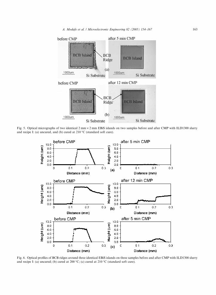
Fig. 5. Optical micrographs of two identical 2 mm · 2 mm EBiS islands on two samples before and after CMP with ILD1300 slurryand recipe I: (a) uncured, and (b) cured at 210 �C (standard soft cure).
Fig. 6. Optical profiles of BCB ridges around three identical EBiS islands on three samples before and after CMP with ILD1300 slurryand recipe I: (a) uncured; (b) cured at 200 �C; (c) cured at 210 �C (standard soft cure).
A. Modafe et al. / Microelectronic Engineering 82 (2005) 154–167 163
Fig. 7. Scanning electron micrographs (SEMs) showing thecross section of a 5 mm · 10 mm, 12-lm deep EBiS island afterdeposition of two BCB layers and planarization. Thin layers ofchromium (Cr) and gold (Au)were sputtered on the wafer to helpwith taking the SEM and to test the adhesion of metal layers.
164 A. Modafe et al. / Microelectronic Engineering 82 (2005) 154–167
blanket BCB film, as discussed in Section 3, about2–3 min of polishing time should have been en-ough to remove the ridges.
In order to fill the depression, the second BCBlayer is spun on and patterned. At this point, thefilms should be partially cured at a temperatureclose to the activation temperature of BCB poly-merization. The curing helps with cross-linkingof the BCB layers. If the cure temperature is toolow, the top BCB layer is peeled off during theCMP. On the other hand, if the cure temperatureis too high, the CMP removal rate of the BCBridges is too low. However, since a ridge ismechanically weaker than a blanket film, the re-moval rate of cured BCB ridges is much higherthan the removal rate of blanket films. As Figs. 5and 6(b) show the soft-cured BCB ridges werenot completely removed after 12 min of CMP (rec-ipe I with ILD1300 slurry). The average removalrate was measured to be 0.3 lm/min. To furtherincrease the removal rate of the ridges, the BCBfilm was cured at temperatures lower than thestandard soft cure (210 �C). The removal of the200 �C-cured BCB ridges, as shown in Fig. 6(c),was much faster, with an average removal rate of0.9 lm/min. We were able to increase the removalrate of the cured BCB ridges up to 2.4 lm/minwith no peel-off by lowering the cure temperatureto 184 �C.
Finally, as shown in Fig. 4(e), the BCB islandsare planarized using CMP, providing a planar sur-face for the subsequent process steps. Dependingon the subsequent processes, a soft cure (at210 �C for 40 min) or a hard cure (at 250 �C for60 min) of BCB polymer is performed at the endof the process. Fig. 7 shows scanning electronmicrographs (SEMs) of the cross-section of a com-pleted EbiS island. The island is 12 lm deep withan area of 5 mm · 10 mm.
In order to study how the planarity of the EBiSislands evolves during the fabrication, we mea-sured the island depth and the BCB ridge heightbefore and after each BCB film deposition and be-fore and after each CMP run. The measurementwas performed on four wafers (A, B, C, and D)with islands of two different sizes, 5 mm · 14 mmand 5 mm · 20 mm. The islands were etched usingDRIE to an average depth of 26.8 lm. Fig. 8
shows how the average island depression depthin each wafer changes after each step. Two layersof BCB polymer were deposited and three CMPruns were performed. The average island depres-sion depth was reduced to below 2 lm. It is clearfrom the trend of reduction in the depressiondepth that with another BCB layer depositionand CMP run, the average island depression canbe reduced to close to zero. Although the mechan-ical abrasion is negligible in a depression, an in-crease in the depression depth is observed aftereach CMP step. This shows that ILD1300 slurrycan chemically remove BCB polymer from the is-land area. Fig. 9 shows the changes of the averageBCB ridge height in each wafer after each step.

Fig. 8. Average island depression in different steps of EBiS process for four test wafers.
Fig. 9. Average BCB ridge heights in different steps of EBiS process for four test wafers.
A. Modafe et al. / Microelectronic Engineering 82 (2005) 154–167 165
The average height was reduced to less than 1 lmand could be reduced even more with a longerCMP at the end. In order to quantify the planari-
zation of the EBiS process, we calculated the totalstep height reduction (T-SHR) in each step foreach wafer. T-SHR is given by
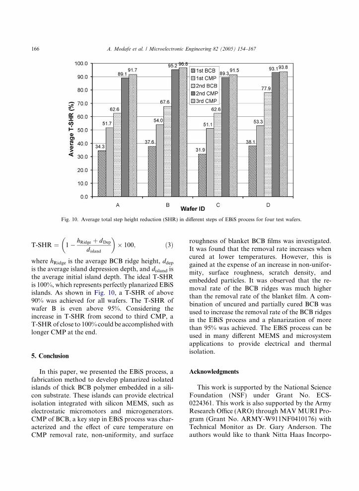
Fig. 10. Average total step height reduction (SHR) in different steps of EBiS process for four test wafers.
166 A. Modafe et al. / Microelectronic Engineering 82 (2005) 154–167
T-SHR ¼ 1� hRidge þ dDep
d island
� �� 100; ð3Þ
where hRidge is the average BCB ridge height, ddepis the average island depression depth, and disland isthe average initial island depth. The ideal T-SHRis 100%, which represents perfectly planarized EBiSislands. As shown in Fig. 10, a T-SHR of above90% was achieved for all wafers. The T-SHR ofwafer B is even above 95%. Considering theincrease in T-SHR from second to third CMP, aT-SHRof close to 100%could be accomplishedwithlonger CMP at the end.
5. Conclusion
In this paper, we presented the EBiS process, afabrication method to develop planarized isolatedislands of thick BCB polymer embedded in a sili-con substrate. These islands can provide electricalisolation integrated with silicon MEMS, such aselectrostatic micromotors and microgenerators.CMP of BCB, a key step in EBiS process was char-acterized and the effect of cure temperature onCMP removal rate, non-uniformity, and surface
roughness of blanket BCB films was investigated.It was found that the removal rate increases whencured at lower temperatures. However, this isgained at the expense of an increase in non-unifor-mity, surface roughness, scratch density, andembedded particles. It was observed that the re-moval rate of the BCB ridges was much higherthan the removal rate of the blanket film. A com-bination of uncured and partially cured BCB wasused to increase the removal rate of the BCB ridgesin the EBiS process and a planarization of morethan 95% was achieved. The EBiS process can beused in many different MEMS and microsystemapplications to provide electrical and thermalisolation.
Acknowledgments
This work is supported by the National ScienceFoundation (NSF) under Grant No. ECS-0224361. This work is also supported by the ArmyResearch Office (ARO) through MAVMURI Pro-gram (Grant No. ARMY-W911NF0410176) withTechnical Monitor as Dr. Gary Anderson. Theauthors would like to thank Nitta Haas Incorpo-
A. Modafe et al. / Microelectronic Engineering 82 (2005) 154–167 167
rated for supplying the ILD1300 slurry and polish-ing pads. We would also like to thank Mr. ThomasC. Loughran and Mr. Nolan A. Ballew for helpwith fabrication, Mr. Wen-Hsien Chuang for helpwith the SEM pictures, and Dr. Madhumita Dattafor help with the AFM measurements, all fromUniversity of Maryland.
References
[1] A.H. Epstein, et al., in: Digest Tech. Papers 9th Interna-tional Conference Solid-State Sensors and Actuators(Transducers�97), 1997, pp. 753–756.
[2] A.H. Epstein, et al., in: Proceedings of the EighthInternational Symposium on Transport Phenomena andDynamics of Rotating Machinery (ISROMAC�8), 2000.
[3] R. Ghodssi, et al., in: Digest Tech. Papers 10th Interna-tional Conference on Solid-State Sensors and Actuators(Tansducers�99), 1999, pp. 1456–1459.
[4] X. Zhang, et al., in: Solid-State Sensor and ActuatorWorkshop, 2000, pp. 316–319.
[5] K.-S. Chen et al., J. Micromech. Microeng. 12 (2002) 714–722.
[6] M. Raieszadeh, et al., in: Proceedings of the 18th Interna-tional Conference on Micro Electro Mechanical Systems(MEMS�05), 2005, pp. 199–202.
[7] G. Barillaro et al., Sens. Actuat. A 107 (2003) 279–284.[8] C. Zhang, K. Najafi, J. Micromech. Microeng. 14 (2004)
769–774.[9] A. Modafe et al., IEEE Trans. Dev. Mater. Reliab. 4
(2004) 495–508.[10] R.A. Kirchhoff, K.J. Bruza, Prog. Polym. Sci. 18 (1993)
85–185.[11] M.F. Farona, Prog. Polym. Sci. 21 (1996) 505–555.[12] M.E. Mills et al., Microelectron. Eng. 33 (1997) 327–
334.
[13] T.-K.A. Chou, K. Najafi, in: Digest Tech. Papers 11thInternational Conference on Solid-State Sensors andActuators (Tansducers�01), 2001, pp. 1570–1773.
[14] S. Guo, Proc. SPIE VII (2003) 422–429.[15] N. Ghalichechian et al., J. Vac. Sci. Technol. B 22 (2004)
2439–2447.[16] A. Modafe, et al., in: MRS Spring Meeting: Chemical–
Mechanical Planarization – Integration, Technology, andReliability Symposium, 2005.
[17] A. Modafe, et al., in: AVS 51st International Symposium,2004.
[18] J.M. Steigerwald et al., Chemical Mechanical Planariza-tion of Microelectronic Materials, Wiley, New York, 1997.
[19] C.L. Borst et al., Chemical–Mechanical Polishing of LowDielectric Constant Polymers and Organosilicate Glasses,Kluwer Academic Publishers, Dordrecht, 2002, p. 48.
[20] J.M. Steigerwald et al., Chemical–Mechanical Planariza-tion of Microelectronic Materials, Wiley, New York, 1997,p. 49.
[21] N.J. Brown et al., Proc. SPIE (1981) 42–57.[22] F.G. Shi, B. Zhao, Appl. Phys. A 67 (1998) 249–252.[23] T.K. Doy et al., J. Electrochem. Soc. 151 (2004) G196–
G199.[24] Y.-R. Jeng, P.-Y. Huang, Electrochem. Solid-State Lett. 7
(2004) G40–G43.[25] Q. Luo et al., Thin Solid Films 335 (1998) 160–167.[26] E. Paul, J. Electrochem. Soc. 148 (2001) G355–G358.[27] E. Paul, J. Electrochem. Soc. 149 (2002) G305–G308.[28] E. Paul, R. Vacassy, J. Electrochem. Soc. 150 (2003)
G739–G743.[29] S. Thagella et al., J. Electrochem. Soc. 151 (2004) G205–
G215.[30] J.M. Neirynck, in: Proceedings of the 23rd International
Conference on Metallurgical Coatings and Thin Films:Thin Solid Films, 1996, pp. 447–452.
[31] R.W. Johnson et al., IEEE Trans. Compon. HybridManufact. Technol. 13 (1990) 347–352.
[32] D.C. Burdeaux et al., J. Electron. Mater. 19 (1990) 1357–1366.