Fabrication of a carbon nanotube-embedded silicon nitride membrane for studies of nanometer-scale...
20
UCRL-JRNL-206270 Fabrication of a Carbon Nanotube-Embedded Silicon Nitride Membrane for Studies of Nanometer-Scale Mass Transport J. K. Holt, A. Noy, T. Huser, D. Eaglesham, O. Bakajin August 27, 2004 Nanoletters
-
Upload
independent -
Category
Documents
-
view
3 -
download
0
Transcript of Fabrication of a carbon nanotube-embedded silicon nitride membrane for studies of nanometer-scale...

UCRL-JRNL-206270
Fabrication of a CarbonNanotube-Embedded Silicon NitrideMembrane for Studies ofNanometer-Scale Mass Transport
J. K. Holt, A. Noy, T. Huser, D. Eaglesham, O.Bakajin
August 27, 2004
Nanoletters

Disclaimer
This document was prepared as an account of work sponsored by an agency of the United States Government. Neither the United States Government nor the University of California nor any of their employees, makes any warranty, express or implied, or assumes any legal liability or responsibility for the accuracy, completeness, or usefulness of any information, apparatus, product, or process disclosed, or represents that its use would not infringe privately owned rights. Reference herein to any specific commercial product, process, or service by trade name, trademark, manufacturer, or otherwise, does not necessarily constitute or imply its endorsement, recommendation, or favoring by the United States Government or the University of California. The views and opinions of authors expressed herein do not necessarily state or reflect those of the United States Government or the University of California, and shall not be used for advertising or product endorsement purposes.
Fabrication of a Carbon Nanotube-Embedded Silicon
Nitride Membrane for Studies of Nanometer-Scale
Mass Transport
Jason K. Holt*, Aleksandr Noy, Thomas Huser, David Eaglesham, and Olgica Bakajin
Biosecurity and Nanosciences Laboratory, Lawrence Livermore National Laboratory, 7000 East
Avenue, Livermore, CA 94551
Received Date
Phone: 925-422-6573
Fax: 925-423-0579
*corresponding author

2
Table of Contents Graphic
300 nm300 nm

3
ABSTRACT
A membrane consisting of multiwall carbon nanotubes embedded in a silicon nitride matrix was
fabricated for fluid mechanics studies on the nanometer scale. Characterization by tracer diffusion and
scanning electron microscopy suggests that the membrane is free of large voids. An upper limit to the
diffusive flux of D2O of 2.4x10⁻⁸ mole/m2-s was determined, indicating extremely slow transport. By
contrast, hydrodynamic calculations of water flow across a nanotube membrane of similar specifications
predict a much higher molar flux of 1.91 mole/m2-s, suggesting that the nanotubes produced possess a
“bamboo” morphology. The carbon nanotube membranes were used to make nanoporous silicon nitride
membranes, fabricated by sacrificial removal of the carbon. Nitrogen flow measurements on these
structures give a membrane permeance of 4.7x10⁻⁴ mole/m2-s-Pa at a pore density of 4x1010 cm-2.
Using a Knudsen diffusion model, the average pore size of this membrane is estimated to be 66 nm,
which agrees well with TEM observations of the multiwall carbon nanotube outer diameter. These
membranes are a robust platform for the study of confined molecular transport, with applications in
separations and chemical sensing.

4
A number of recent studies1-5 have focused on the development of membranes with nanometer-
scale pores. Such membranes could find application in the area of size-based chemical and biological
separations, provided pore sizes can be reduced to molecular diameters and a high flux of the permeate
molecule can be achieved. On this size scale, however, little is known about the behavior of fluids;
deviations from continuum transport can occur as the channel size becomes comparable to molecular
diameters. For example, it is known that the intra-pore diffusivity (as compared with the bulk
diffusivity) decreases when the pore size becomes comparable to molecular dimensions.6 In electrolyte
solutions, if the pore radius is comparable to the Debye length (electrical double layer thickness), a
situation can arise where the ion concentration within the pore exceeds that of the bulk solution,7 which
may have some interesting consequences for the development of ion-selective membranes.
An ideal system for the study of confined molecular transport is a carbon nanotube, which has an
inner diameter as small as 1 nm. Not surprisingly, a number of recent molecular dynamics simulations
have focused on transport within these materials.8-10 Many exotic predictions have been made, from the
formation of novel phases of ice8 and pulsed one-dimensional water transport,9 to the spontaneous
insertion of ss-DNA into a single wall carbon nanotube.10 What has been lacking, however, is a
platform for experimentally verifying some of these predictions.
One method explored involves chemical vapor deposition of carbon within the pores of an
alumina membrane.2 Typically, the pore sizes achieved by this approach (of order 100 nm) are larger
than the size range of interest for chemical and biological separations. In addition, the inner walls of
these carbon nanotubules are only semigraphitic and thus do not possess the inherent smoothness of a
purely graphitic carbon nanotube (CNT). It is also reported2 that tubes prepared in this manner possess
acidic surface sites (-COOH) on their walls. The inherent smoothness and inertness of a purely
graphitic CNT are the attributes that molecular dynamics simulations11 predict give rise to a high
molecular flux through CNTs.

5
Another method for preparation of such a membrane involves embedding an amorphous carbon
coated graphitic tube in an epoxy matrix.1 However, the resultant pore diameter in these materials is
again large (~150 nm). A method that has managed to produce membranes in the single nanometer size
regime involves creating damage tracks in a polycarbonate film by use of a collimated fission fragment
beam, followed by etching in basic solution.3 With subsequent electroless plating, single gold
nanotubes of order 2 nm were prepared. More recently, a polystyrene-coated CNT membrane was
fabricated.5 The pore sizes of this membrane are reported to be consistent with that of multiwall CNT
inner diameters (~ 7.5 nm).
The method described in this study involves producing a CNT-based membrane using low-stress
silicon nitride as a conformal matrix material. To the author’s knowledge, this research constitutes the
first attempt at producing a truly graphitic CNT membrane using a ceramic matrix material. In contrast
to polymer matrices, silicon nitride has a negligible molecular permeability, leaving the cores of
embedded CNTs as the only pores in the membrane. Alternatively, these nanotubes can serve as a
template for the production of nanoporous silicon nitride by selectively removing them via oxidation.
The other advantage offered by silicon nitride is its vapor phase deposition. Polymers spun-on to CNT
arrays require elaborate curing processes5 to reduce CNT agglomeration and ensure retention of
alignment.
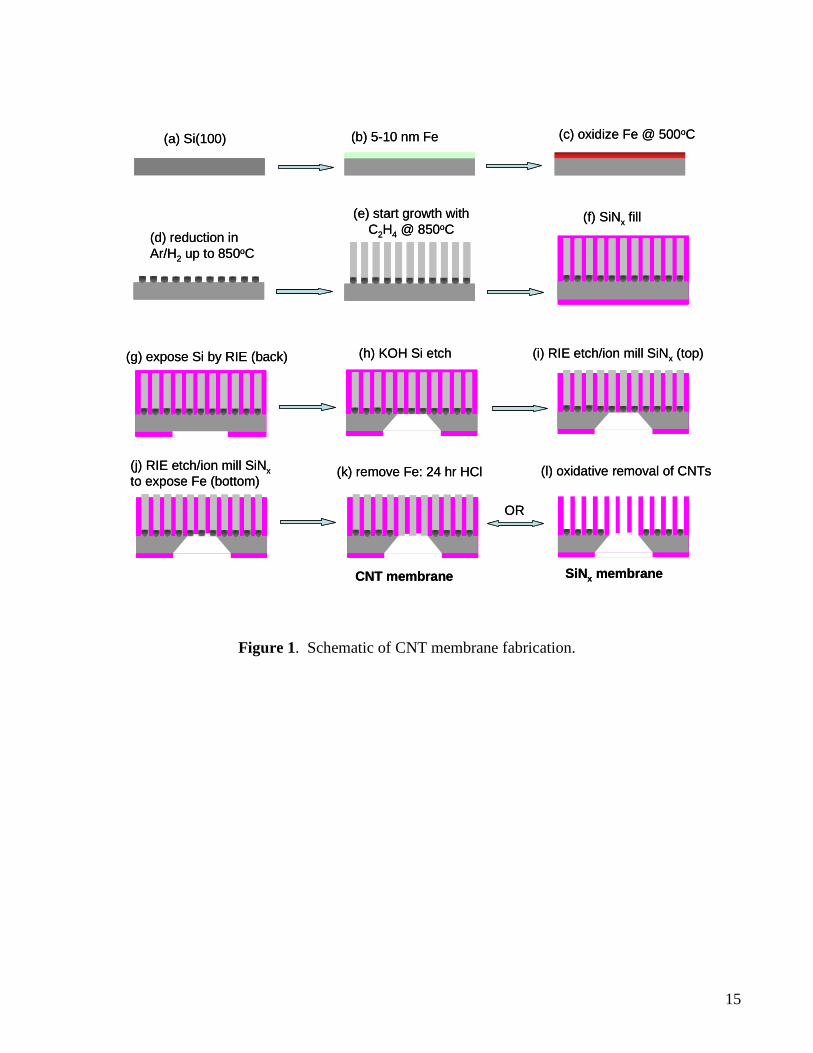
The entire fabrication process for these membranes is illustrated in Fig. 1. Our starting material
is single-side polished test grade Si(100). The catalyst used for nanotube growth is iron, deposited by
electron beam evaporation to a thickness between 2.5-5.0 nm. The samples are annealed shortly after
the deposition of iron (500oC, 1 hour, 10 sccm O2) to oxidize the surface, a common practice.12 We
have observed that samples which undergo room temperature oxidation in air over several days have a
reduced catalytic efficiency, producing a lower density array of nanotubes. Samples are next placed
into an atmospheric pressure CVD system (1” diameter tube furnace) and initially exposed to a reducing

6
environment of Ar/H2 (600 sccm/400 sccm) as the temperature is ramped up to the growth temperature
of 850oC for a period of 20 minutes. At this point, discrete iron nanoparticles form, with diameters in
the range from 20-100 nm. The diameter distribution is skewed towards smaller particles as the iron
thickness is decreased. These nanoparticles serve as the catalyst and nucleation sites for nanotube
growth. After temperature stabilization, C2H4 (1000 sccm) is introduced to initiate growth. Nanotube
growth occurs for 20 minutes and results in a dense array of multiwall nanotubes of ~ 5-10 µm length
and 20-50 nm diameter, as shown in Fig. 2a; tube areal densities are typically 4x1010 cm-2. The crucial
step in our process is filling the voids between the nanotubes with a rigid, impermeable material that
conforms to them, to enable further processing into a membrane. Low-stress silicon nitride possesses
these desirable properties. After tube growth, the samples are placed into a low pressure CVD furnace
to deposit a low-stress silicon nitride layer, using a deposition temperature of 800oC and a 6:1 ratio of
dichlorosilane to ammonia. A target film thickness between 400-800 nm was found sufficient to fill the
bulk of the 5-10 µm thick nanotube forest and encapsulate the top. Due to the non-oxidizing
atmosphere for the silicon nitride process, carbon nanotube damage is not observed at these elevated
temperatures and the tubes retain their alignment through the process. Also, there is little concern over
the filling of the nanotube interior with silicon nitride, as we have observed by transmission electron
microscopy (TEM) that the nanotubes grow with a graphitic cap at the top. The excellent coverage
offered by this material can be seen in the image of Fig. 2b, where the film (partially fractured by
preparation of the cross section) is seen to encapsulate an individual nanotube.
A number of additional processing steps are required before continuous, open channels can be
formed. Reactive ion etching (RIE), using a 3.6:1 ratio of CF4:O2 at 150 W power, is used to open a
window in the silicon nitride layer to expose the backside of the silicon substrate. This is followed by
anisotropic KOH etching of the exposed silicon to uncover the nanotube/silicon nitride film. To remove
excess silicon nitride deposited atop the CNTs (opposite the silicon substrate), as well as open their tips,

7
RIE is used once again. Alternatively, Ar-ion milling can be used under conditions of 0.5 kV ion
energy and 1 mA/cm2 beam current density; due to the lack of chemical selectivity, this process
typically produces a much smoother surface. It is important that this tube-opening step occurs after the
KOH wet processing to avoid the possibility that the exposed carbon nanotubes are filled by liquids.
Examination of the interface where the silicon was removed by KOH etching (referred to as the
“backside” of the membrane) reveals a number of bright particles (Fig. 2c), which were confirmed by
Energy Dispersive X-ray (EDX) analysis to contain iron. Consideration of their size (20-50 nm),
comparable to the outer diameter of the carbon nanotubes, suggests that these are residual iron catalyst
particles not removed during the prior processing steps. As many of these particles would block access
to the core of the nanotube, a strategy for their removal was devised. This consists of a brief RIE
process (or the aforementioned ion milling process) to remove a few nm of silicon nitride and further
expose the iron nanoparticles. Fig. 2c depicts the backside of the membrane after the ion milling
process, with pores of 40-90 nm evident, comparable in size to the iron nanoparticles and the nanotube
outer diameter. After the etching/ion milling step, the iron nanoparticles are removed by immersion of
the sample in concentrated HCl for 24 hours. Subsequent EDX analysis confirmed the removal of the
vast majority (>90%) of the nanoparticles. At this stage, the carbon nanotube membrane fabrication is
complete. If a nanoporous silicon nitride membrane is desired instead, the nanotubes can be removed
by an oxidation treatment (800oC, 10 sccm O2, 1 hour).
The mechanical integrity of these membranes is a critical issue for their subsequent
characterization. Due to the inherent brittle nature of ceramic materials like silicon nitride, voids that
remain after processing (due to incomplete coverage of the nanotube array) can lead to cracks and
ultimately fracture the membrane; Fig. 2d is a cross-sectional image of the membrane in which such
voids in the interior of the membrane are evident. However, the CNTs may provide a modest
reinforcement effect, as the work of Ma et al.13 on multiwall CNT-silicon carbide composites suggests,
by deflecting cracks that might otherwise propagate and rupture the membrane. To test the mechanical
8
integrity of the CNT-silicon nitride composites fabricated in this study, fully processed CNT membranes
were mounted in an O-ring sealed fixture with one side open to air and the other placed under vacuum.
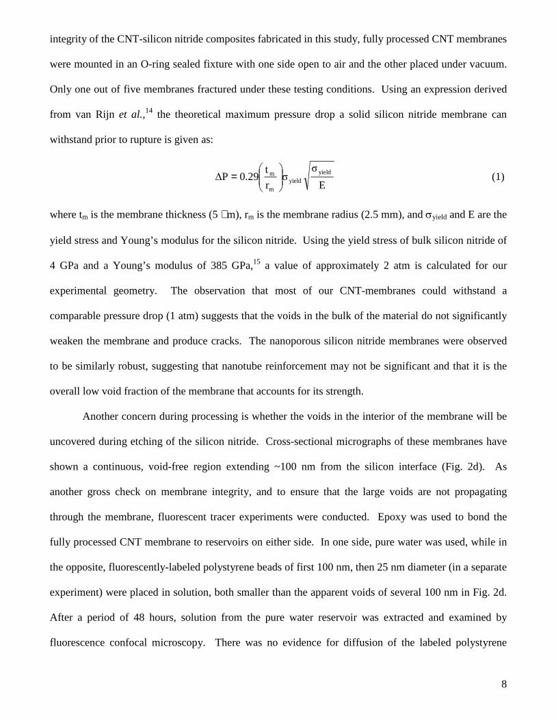
Only one out of five membranes fractured under these testing conditions. Using an expression derived
from van Rijn et al.,14 the theoretical maximum pressure drop a solid silicon nitride membrane can
withstand prior to rupture is given as:
E
σσr
t0.29∆P yield
yieldm
m
= (1)
where tm is the membrane thickness (5 µm), rm is the membrane radius (2.5 mm), and σyield and E are the
yield stress and Young’s modulus for the silicon nitride. Using the yield stress of bulk silicon nitride of
4 GPa and a Young’s modulus of 385 GPa,15 a value of approximately 2 atm is calculated for our
experimental geometry. The observation that most of our CNT-membranes could withstand a
comparable pressure drop (1 atm) suggests that the voids in the bulk of the material do not significantly
weaken the membrane and produce cracks. The nanoporous silicon nitride membranes were observed
to be similarly robust, suggesting that nanotube reinforcement may not be significant and that it is the
overall low void fraction of the membrane that accounts for its strength.
Another concern during processing is whether the voids in the interior of the membrane will be
uncovered during etching of the silicon nitride. Cross-sectional micrographs of these membranes have
shown a continuous, void-free region extending ~100 nm from the silicon interface (Fig. 2d). As
another gross check on membrane integrity, and to ensure that the large voids are not propagating
through the membrane, fluorescent tracer experiments were conducted. Epoxy was used to bond the
fully processed CNT membrane to reservoirs on either side. In one side, pure water was used, while in
the opposite, fluorescently-labeled polystyrene beads of first 100 nm, then 25 nm diameter (in a separate
experiment) were placed in solution, both smaller than the apparent voids of several 100 nm in Fig. 2d.
After a period of 48 hours, solution from the pure water reservoir was extracted and examined by
fluorescence confocal microscopy. There was no evidence for diffusion of the labeled polystyrene

9
beads in either experiment, suggesting that these voids in the membrane interior do not propagate
through, leaving the nanotube interior as the most likely conduit for molecular transport. These
measurements were followed by isotopic tracer measurements where deuterated water (D2O) was placed
in one reservoir, with pure water in the other. After a period of 24 hours, a sample was extracted from
the pure water reservoir and analyzed by stable isotope mass spectrometry, with a sensitivity of
approximately 1 part per million deuterium relative to hydrogen.16 There was no evidence for diffusion
of D2O in this case, which provides an upper bound on the rate of permeation through our membranes of
2.4x10⁻⁸ mole/m2-s (as determined by the sensitivity of the analytical technique). This is in sharp
contrast to the flux of 0.29 mole/m2-s, calculated by molecular dynamics simulations for diffusion
through considerably smaller single wall carbon nanotubes.9 If indeed the only open channels in this
experiment consisted of the interior of the carbon nanotubes, a measurable flux of D2O would have been
expected. The low flux observed here suggests that this channel is blocked. Specifically, it is possible
that the CNTs in this membrane are not hollow and instead form the well-known “bamboo”
morphology,17 consisting of periodically spaced chambers along their length. In the literature,
characterization of the nanotube morphology is often based on TEM of a small fraction (~100 nm) of
the entire length (often in excess of 10 µm). Thus, it seems probable that even the nominally hollow
tubes reported in the literature may in fact be blocked. The CNTs in this study show evidence of the
“bamboo” morphology, as can be seen in the TEM micrograph of Fig. 3.
To produce open, nanometer-scale channels through which molecular transport could be
measured, a carbon nanotube membrane was placed into an oxygen furnace (800oC, 1 hour, 10 sccm O2)
to allow selective oxidation of the nanotubes. The resulting nanoporous silicon nitride membrane was
then mounted in an O-ring sealed flow cell with a mass flow controller and pressure gauge upstream of
the membrane. A pressurized nitrogen line was attached upstream, with the other end open to air. A
control experiment utilizing a non-porous material of similar dimensions confirmed that all connections
were leak tight, such that the membrane would be the only gas transport path. By measuring the flow

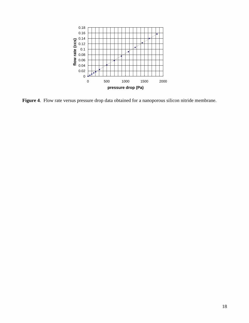
10
rate as a function of pressure drop (see Fig. 4), the permeance of the membrane could be determined.
For pressure drops in the range from 50-1800 Pa (0.007-0.27 psi), a permeance of 4.7x10⁻⁴ mole/m2-s-
Pa was determined. This compares with a value of 2.6x10⁻⁶ mole/m2-s-Pa, determined for a multiwall
CNT membrane with pores reported to be 7.5 nm in diameter5, in the range expected of CNT inner
diameters. Given that the membrane in this study was created by oxidative removal of the CNTs, we
would expect larger pores, representative of CNT outer diameters, which in turn should lead to a larger
membrane permeance. Data obtained from TEM measurements (Fig. 3) suggests a size distribution of
CNT outer diameters ranging from 20-50 nm. To determine whether the measured membrane
permeance can be accounted for by pores in the size range of the CNT outer diameter, we have to
consider a model for molecular transport.
The behavior of fluids on the size scale of these membrane pores is expected to differ from that
of bulk, continuum transport. In particular, a comparison of the mean free path at 1 atm for nitrogen (66
nm) with that of the nitride pore size (20-50 nm) suggests a transitional flow regime, between slip and
free-molecule flow.18 Previous work by Itaya et al.19 with alumina membranes has shown that Knudsen
diffusion can adequately characterize molecular transport down to 10 nm length scales. Thus, assuming
Knudsen diffusion, where gas-solid collisions are treated as elastic and result in diffuse scattering, the
gas molar flux across the membrane is linear in pressure drop:
PMRT2
CπrJ
2
∆
= πρ
gV (2)
where r is the pore radius, M is the molecular weight, R is the gas constant, T is temperature, ρ is the
pore areal density, Vg is the gas molar volume, ∆P is the pressure drop, and C is an aspect ratio
dependent factor ≈ (1+0.46•L/r)-1,20 with L being the effective diffusion length. Using the
experimentally measured permeance P (= J/∆P) of the nanoporous silicon nitride membrane, along with
other membrane parameters, in the limit L>>r, the average pore radius can be determined as follows:

11
31
ρLMT1.1
r
= P (3)
For a typical membrane pore density of 4x1010cm-2 and an effective diffusion length of 10 µm
(accounting for the membrane thickness and nanotube tortuosity), an average pore diameter of 66 nm is
determined. This value is slightly larger, but comparable to the outer diameter of CNTs observed by
TEM. This larger-than-expected value could be accounted for by tightly bundled CNTs that could not
be filled by the silicon nitride. For reference, the permeance of a microporous alumina filter (Whatman
Anodisc) of 200 nm nominal pore diameter (60 µm thickness, 1.6x109cm-2 pore density) was measured,
and the Knudsen diameter calculated from this measurement was ~180 nm, similar to SEM observations
of the pore size. For considerably smaller pores (in the 1 nm range of single wall nanotubes), it is
expected that the molecule-pore interaction will differ from the simple elastic collision model assumed
in Knudsen diffusion. In particular, we expect to see a dependence on the molecular coverage of the
surface. Modeling and experiments in this size regime will be the subject of future studies.
Also of interest for subsequent liquid experiments is an estimate of the flux of water across a
nanotube membrane. The method of van Rijn et al.21 was used for this calculation, which assumes
viscous, laminar flow and includes correction factors for frictional losses with the walls, interference
effects of neighboring pores, and neglects any nonviscous kinetic losses. Under these assumptions, in
the limit L>>r, the water molar flux is given as:
PL
0.12rJ
2
∆
=wVµ
(4)
where µ is the liquid viscosity, Vw is the molar volume of water, and all other variables are defined as
before. For a 10 nm inner diameter nanotube of 10 µm length and a pressure drop of 1 atm, a water flux
of 1.91 mole/m2-s is calculated. For a 1 nm inner diameter nanotube, the corresponding water flux is
0.019 mole/m2-s, an order of magnitude less than the 0.29 mole/m2-s value determined for a similar size

12
single wall nanotube, using molecular dynamics-based transport rates.9 However, it is unclear whether
the assumption of no-slip along the walls, used in the hydrodynamic model, is satisfied for the smooth,
hydrophobic interior of a carbon nanotube,22 and this alone may account for the discrepancy in these
two values. This is a topic under active investigation.
In summary, a robust, void-free membrane that can be used for the study of nanofluidics has
been developed by standard microfabrication techniques, consisting of multiwall carbon nanotubes
embedded in a silicon nitride matrix. A nanoporous silicon nitride membrane was formed by the
oxidative removal of these carbon nanotubes from the silicon nitride matrix. The gas permeability of
this nanoporous silicon nitride membrane was confirmed and the nitrogen permeance determined.
Assuming Knudsen-type diffusion through the membrane, an average pore size of 66 nm is calculated,
which is comparable to that of the multiwall nanotube outer diameter. The calculated rate of water
transport (in the hydrodynamic limit) of 1.91 mole/m2-s through a smaller pore nanotube membrane
suggests that the structure would be suitable for liquid-based experiments and potential nanofluidic
devices. Future studies are geared towards controlling deposition parameters to suppress the formation
of “bamboo” CNTs, as well as fabrication of an analogous single wall nanotube membrane, which
should bring us closer to verifying some of the exotic molecular transport properties predicted for
CNTs.
Acknowledgement. This work was performed under the auspices of the US Department of Energy
by UC, LLNL under contract No. W-7405-Eng-48 with funding from the Laboratory Directed Research
and Development program. The author thanks Gail Eaton for assistance with stable isotope
mass spectrometry measurements.
References

13
(1) Sun, L.; Crooks, R. M., J. Am. Chem. Soc. 2000, 122, 12340-12345.
(2) Miller, S. A.; Young, V. Y.; Martin, C. R., JACS 2001, 123, 12335-12342.
(3) Harrell, C. C.; Lee, S. B.; Martin, C. R., Anal. Chem. 2003, 75, 6861-6867.
(4) Cooper, S. M.; Cruden, B. A.; Meyyappan, M.; Raju, R.; Roy, S., Nano Lett. 2004, 4, 377-381.
(5) Hinds, B. J.; Chopra, N.; Rantell, T.; Andrews, R.; Gavalas, V.; Bachas, L. G., Science 2004, 303,
62-65.
(6) Deen, W. M., AIChE J. 1987, 33, 1409-1425.
(7) Cerver, J; Manzanares, J.A.; Mafe, S., J. Membrane Sci. 2001, 191, 179-187
(8) Koga, K.; Gao, G. T.; Tanaka, H.; Zeng, X. C., Nature 2001, 412, 802-805.
(9) Hummer, G.; Rasaiah, J. C.; Noworyta, J. P., Nature 2001, 414, 188-190.
(10) Gao, H.; Kong, Y.; Cui, D.; Ozkan, C., Nano Lett. 2003, 3, 471-473.
(11) Skoulidas, A. L.; Ackerman, D. M.; Johnson, J. K.; Sholl, D. S., Phys. Rev. Lett. 2002, 89,
185901-1-185901-4.
(12) Fan, S.; Chapline, M. G.; Franklin, N. R.; Tombler, T. W.; Cassell, A. M.; Dai, H., Science 1999,
283, 512-514.
(13) Ma, R. Z.; Wu, J.; Wei, B. Q.; Liang, J.; Wu, D. H., J. Mater. Sci. 1998, 33, 5243-5246.
(14) Rijn, C. J. M.; Wekken, M.; Nijdam, W.; Elwenspoek, M., J. Microelectromech. Syst. 1997, 6,
48-54.
(15) Tong, H.; Jansen, H.; Gadgil, V.; Bostan, C.; Berenshot, E.; Rijn, C. J. M.; Elwenspoek, M.,
Nano. Lett. 2004, 4, 283.
14
(16) Eaton, G., private communication.
(17) Cui, H.; Zhou, O.; Stoner, B. R., J. Appl. Phys. 2001, 88, 6072-6074.
(18) Bird, G. A., Molecular Gas Dynamics, Clarendon Press: Oxford, United Kingdom, 1976.
(19) Itaya, K.; Sugawara, S.; Arai, K.; Saito, S., J. Chem. Eng. Jpn. 1984, 17, 514.
(20) Elwenspoek, M. C.; Jansen, H. V., Silicon Micromachining, Cambridge Univ. Press: Cambridge,
England, pp 216-355, 1998.
(21) Rijn, C. J. M.; Elwenspoek, M., IEEE Conf. MEMS ’95, 1995; pp 83-87.
(22) Zhu, Y.; Granick, S., Phys. Rev. Lett. 2002, 88, 106102.
15
Figure 1. Schematic of CNT membrane fabrication.
(a) Si(100) (b) 5-10 nm Fe (c) oxidize Fe @ 500oC
(d) reduction in Ar/H2 up to 850oC
(e) start growth with C2H4 @ 850oC
(f) SiNx fill
(g) expose Si by RIE (back) (h) KOH Si etch (i) RIE etch/ion mill SiNx (top)
(j) RIE etch/ion mill SiNxto expose Fe (bottom)
(k) remove Fe: 24 hr HCl (l) oxidative removal of CNTs
OR
CNT membrane SiNx membrane

16
Figure 2. (a) as-grown array of multiwalled CNTs, (b) CNTs encapsulated by a silicon nitride layer, (c)
backside of membrane after KOH/ion milling treatment; bright particles were confirmed by EDX to be
residual iron not removed after the acid treatment, (d) cross-sectional image of silicon nitride-covered
CNTs; the void-free region of the membrane is denoted by the dashed line; individual CNTs can be
distinguished as white lines in the image.
5 µµµµm
a c
5 µµµµm5 µµµµm
300 nm
B
1 µµµµm
D
500 nm
5 µµµµm
A
C
B
300 nm
500 nm

17
Figure 3. TEM image of a multiwall CNT produced by thermal CVD; arrows indicate graphitic shells
that block the interior of the tube, characteristic of “bamboo” CNTs; the dark material is iron catalyst
that has migrated to the interior of the tube.
50nm50nm
18
Figure 4. Flow rate versus pressure drop data obtained for a nanoporous silicon nitride membrane.
0
0.02
0.04
0.06
0.08
0.1
0.12
0.14
0.16
0.18
0 500 1000 1500 2000
pressure drop (Pa)
flo
w r
ate
(ccs
)