Porous Dual-Layered MoOx Nanotube Arrays with Highly ...
11
Porous Dual-Layered MoO x Nanotube Arrays with Highly Conductive TiN Cores for Supercapacitors Xiang Peng, [a, c] Kaifu Huo,* [a] Jijiang Fu, [b] Biao Gao, [b] Lei Wang, [a] Liangsheng Hu, [b, c] Xuming Zhang, [c] and Paul K. Chu [c] Porous dual-layered molybdenum oxide (MoO x ) nanotube arrays (NTAs) with highly conductive titanium nitride (TiN) cores (MoO x /TiN/MoO x NTAs) are fabricated by depositing MoO x on porous TiN NTAs produced by nitriding as-anodized TiO 2 NTAs on Ti foils. The highly conductive TiN facilitates elec- tron transfer and the porous MoO x wall allows the electrolyte to permeate the nanotubes readily, maximizing the active sites of the MoO x electroactive material to improve the specific ca- pacitance and rate capability. The coaxial MoO x /TiN/MoO x NTA electrode shows a high specific capacitance of 97 mF cm 2 (323 F g 1 ) at a current density of 1 mA cm 2 , and 60 % capaci- tance is retained when the current density is increased 20 times. A symmetrical device based on the MoO x /TiN/MoO x NTA electrode exhibits a capacitance as high as 24 F cm 3 (based on the volume of MoO x /TiN/MoO x NTAs) and no significant decay is observed after charging/discharging for 10 000 cycles. Electrochemical capacitors or supercapacitors (SCs) boasting superior power densities and long cycle lifetimes have attract- ed increasing attention, owing to promising applications in hybrid electrical vehicles, as back-up power in portable elec- tronics, as well as in power supplies. [1] However, commercial SCs based on carbon electrodes typically have a relatively low energy density, limiting their application. [2] Many attempts have been devoted to increase the energy density while not sacrificing the power density and cycle lifetime in order to sat- isfy commercial needs. Generally, SCs can be classified into two categories: electrical double-layer capacitors (EDLCs) and pseu- docapacitors, according to the charge-storage mechanism. EDLCs commonly use carbonaceous materials as electrodes, whereas pseudocapacitors utilize redox-active electrode mate- rials. Transition-metal oxides (TMOs) such as manganese oxide, [3] vanadium oxide, [4] iron oxide, [5] NiO, [6] CoO, [7] and mo- lybdenum oxide [8] exhibit high pseudocapacitance and have been widely investigated as electrode materials for pseudoca- pacitors, owing to their multiple oxidation states available for charge storage. [9] Among these oxides, molybdenum oxides, MoO x (2 x 3) have attracted considerable interest as a prom- ising supercapacitive material because of its low cost, nontox- icity, multiple oxidation states, high specific capacitance, and the fact that it is environmentally benign. [8a] However, MoO x alone cannot provide superior capacitive capabilities, owing to poor electrical conductivity, resulting in a low power density and sluggish faradaic redox kinetics. [10] Conversely, recent works have been focused on crystalline MoO x , [3a, 11] mainly be- cause of their stability and excellent electrochemical proper- ties. However, the amorphous phase may offer a rather unique electrochemical behavior in energy-storage applications that may be exploitable in certain device applications. [12] To improve the capacitive properties of MoO x and other TMO-based electrodes, considerable attempts have been made to combine MoO x and other TMOs with conducting nanowires, carbon nanotubes (CNTs), graphene, or reduced graphene oxide on the nanoscale [12a, 13] to overcome the low conductivity of TMOs. Usually, high-performance MoO x -based electrodes are fabricated by mixing MoO x nanowires/nanobelts with conduct- ing CNTs or by depositing MoO x on the conducting nanowire to produce synergistic properties for enhancing capacitive properties. [11a, 14] However, a thin layer or low mass loading of MoO x on conducting nanowires usually leads to low areal and volumetric capacitance. [15] On the other hand, a thick layer or high mass loading generally results in a low rate capability. [12a] In this respect, highly conductive nanotube arrays (NTAs) with open mouths constitute a desirable substrate for loading of MoO x or TMOs, which can be coated on both the inner and outer surfaces of the NTAs. The dual-layered MoO x nanotube coated on both the inner and outer surfaces of the highly con- ductive core could increase the mass loading while keeping a thin and uniform thickness, thus assuring high areal capaci- tance and high rate performance for SCs. In our previous study, we reported porous TiN NTAs on Ti foil for loading poly- aniline (PANI) to form coaxial PANI/TiN/PANI NTAs as high-per- formance electrodes for SCs. [16] The porous TiN NTAs have a high conductivity and provide a large and ion-accessible sur- face area as well as a direct pathway for charge transport, thus they are a promising substrate for loading highly pseudocapa- citive MoO x for high-performance SCs. In this work, porous dual-layered MoO x NTAs with highly conductive TiN cores were prepared through electrochemical [a] X. Peng, Prof. K. Huo, L. Wang Wuhan National Laboratory for Optoelectronics (WNLO) Huazhong University of Science and Technology Wuhan 430074 (China) E-mail : [email protected] [b] Prof. J. Fu, B. Gao, L. Hu The State Key Laboratory of Refractories and Metallurgy Wuhan University of Science and Technology Wuhan 430081 (China) [c] X. Peng, L. Hu, X. Zhang, Prof. P. K. Chu Department of Physics and Materials Science City University of Hong Kong Tat Chee Avenue, Kowloon, Hong Kong (China) Supporting Information for this article is available on the WWW under http://dx.doi.org/10.1002/celc.201402349. ChemElectroChem 2015, 2, 512–517 # 2015 Wiley-VCH Verlag GmbH & Co. KGaA, Weinheim 512 & Communications DOI: 10.1002/celc.201402349
-
Upload
khangminh22 -
Category
Documents
-
view
2 -
download
0
Transcript of Porous Dual-Layered MoOx Nanotube Arrays with Highly ...

Porous Dual-Layered MoOx Nanotube Arrays with HighlyConductive TiN Cores for SupercapacitorsXiang Peng,[a, c] Kaifu Huo,*[a] Jijiang Fu,[b] Biao Gao,[b] Lei Wang,[a] Liangsheng Hu,[b, c]
Xuming Zhang,[c] and Paul K. Chu[c]
Porous dual-layered molybdenum oxide (MoOx) nanotubearrays (NTAs) with highly conductive titanium nitride (TiN)cores (MoOx/TiN/MoOx NTAs) are fabricated by depositingMoOx on porous TiN NTAs produced by nitriding as-anodizedTiO2 NTAs on Ti foils. The highly conductive TiN facilitates elec-tron transfer and the porous MoOx wall allows the electrolyteto permeate the nanotubes readily, maximizing the active sitesof the MoOx electroactive material to improve the specific ca-pacitance and rate capability. The coaxial MoOx/TiN/MoOx NTAelectrode shows a high specific capacitance of 97 mF cm�2
(323 F g�1) at a current density of 1 mA cm�2, and 60 % capaci-tance is retained when the current density is increased 20times. A symmetrical device based on the MoOx/TiN/MoOx NTAelectrode exhibits a capacitance as high as 24 F cm�3 (based onthe volume of MoOx/TiN/MoOx NTAs) and no significant decayis observed after charging/discharging for 10 000 cycles.
Electrochemical capacitors or supercapacitors (SCs) boastingsuperior power densities and long cycle lifetimes have attract-ed increasing attention, owing to promising applications inhybrid electrical vehicles, as back-up power in portable elec-tronics, as well as in power supplies.[1] However, commercialSCs based on carbon electrodes typically have a relatively lowenergy density, limiting their application.[2] Many attemptshave been devoted to increase the energy density while notsacrificing the power density and cycle lifetime in order to sat-isfy commercial needs. Generally, SCs can be classified into twocategories: electrical double-layer capacitors (EDLCs) and pseu-docapacitors, according to the charge-storage mechanism.EDLCs commonly use carbonaceous materials as electrodes,whereas pseudocapacitors utilize redox-active electrode mate-rials. Transition-metal oxides (TMOs) such as manganese
oxide,[3] vanadium oxide,[4] iron oxide,[5] NiO,[6] CoO,[7] and mo-lybdenum oxide[8] exhibit high pseudocapacitance and havebeen widely investigated as electrode materials for pseudoca-pacitors, owing to their multiple oxidation states available forcharge storage.[9] Among these oxides, molybdenum oxides,MoOx (2�x�3) have attracted considerable interest as a prom-ising supercapacitive material because of its low cost, nontox-icity, multiple oxidation states, high specific capacitance, andthe fact that it is environmentally benign.[8a] However, MoOx
alone cannot provide superior capacitive capabilities, owing topoor electrical conductivity, resulting in a low power densityand sluggish faradaic redox kinetics.[10] Conversely, recentworks have been focused on crystalline MoOx,
[3a, 11] mainly be-cause of their stability and excellent electrochemical proper-ties. However, the amorphous phase may offer a rather uniqueelectrochemical behavior in energy-storage applications thatmay be exploitable in certain device applications.[12]
To improve the capacitive properties of MoOx and otherTMO-based electrodes, considerable attempts have been madeto combine MoOx and other TMOs with conducting nanowires,carbon nanotubes (CNTs), graphene, or reduced grapheneoxide on the nanoscale[12a, 13] to overcome the low conductivityof TMOs. Usually, high-performance MoOx-based electrodes arefabricated by mixing MoOx nanowires/nanobelts with conduct-ing CNTs or by depositing MoOx on the conducting nanowireto produce synergistic properties for enhancing capacitiveproperties.[11a, 14] However, a thin layer or low mass loading ofMoOx on conducting nanowires usually leads to low areal andvolumetric capacitance.[15] On the other hand, a thick layer orhigh mass loading generally results in a low rate capability.[12a]
In this respect, highly conductive nanotube arrays (NTAs) withopen mouths constitute a desirable substrate for loading ofMoOx or TMOs, which can be coated on both the inner andouter surfaces of the NTAs. The dual-layered MoOx nanotubecoated on both the inner and outer surfaces of the highly con-ductive core could increase the mass loading while keepinga thin and uniform thickness, thus assuring high areal capaci-tance and high rate performance for SCs. In our previousstudy, we reported porous TiN NTAs on Ti foil for loading poly-aniline (PANI) to form coaxial PANI/TiN/PANI NTAs as high-per-formance electrodes for SCs.[16] The porous TiN NTAs havea high conductivity and provide a large and ion-accessible sur-face area as well as a direct pathway for charge transport, thusthey are a promising substrate for loading highly pseudocapa-citive MoOx for high-performance SCs.
In this work, porous dual-layered MoOx NTAs with highlyconductive TiN cores were prepared through electrochemical
[a] X. Peng, Prof. K. Huo, L. WangWuhan National Laboratory for Optoelectronics (WNLO)Huazhong University of Science and TechnologyWuhan 430074 (China)E-mail : [email protected]
[b] Prof. J. Fu, B. Gao, L. HuThe State Key Laboratory of Refractories and MetallurgyWuhan University of Science and TechnologyWuhan 430081 (China)
[c] X. Peng, L. Hu, X. Zhang, Prof. P. K. ChuDepartment of Physics and Materials ScienceCity University of Hong KongTat Chee Avenue, Kowloon, Hong Kong (China)
Supporting Information for this article is available on the WWW underhttp://dx.doi.org/10.1002/celc.201402349.
ChemElectroChem 2015, 2, 512–517 � 2015 Wiley-VCH Verlag GmbH & Co. KGaA, Weinheim512 &
CommunicationsDOI: 10.1002/celc.201402349
deposition of MoOx on porous TiN NTAs. The TiN NTAs withmesoporous tube wall were obtained through the nitridationof as-anodized TiO2 NTAs,[16] and the amorphous MoOx waselectrochemically deposited into the TiN nanotube along innerand outer surfaces as well as in the mesoporous holes of theTiN nanotube wall, forming a 3D MoOx/TiN/MoOx interconnect-ed network. Such a nanocomposite allows easy permeationand diffusion of the electrolyte into the amorphous MoOx ma-terial to maximize utilization of MoOx, owing to the increasednumber of charge-storage sites. In addition, the high conduc-tivity of TiN provides a direct pathway to transport electronsfrom MoOx to the underlying conductive Ti current collector,thus coaxial MoOx/TiN/MoOx exhibits good capacitive proper-ties, with an areal specific capacitance of about 97 mF cm�2 ata current density of 1 mA cm�2 and a capacitance retention of60 % when the current density is increased 20 times from 1 to20 mA cm�2. Moreover, a symmetrical device based on twoMoOx/TiN/MoOx NTA electrodes exhibits a capacitance as highas 24 F cm�3 (based on the volume of MoOx/TiN/MoOx NTAs)with no significant decay after charging/discharging for 10 000cycles. The MoOx/TiN/MoOx electrode has outstanding proper-ties and promising potential in SC applications.
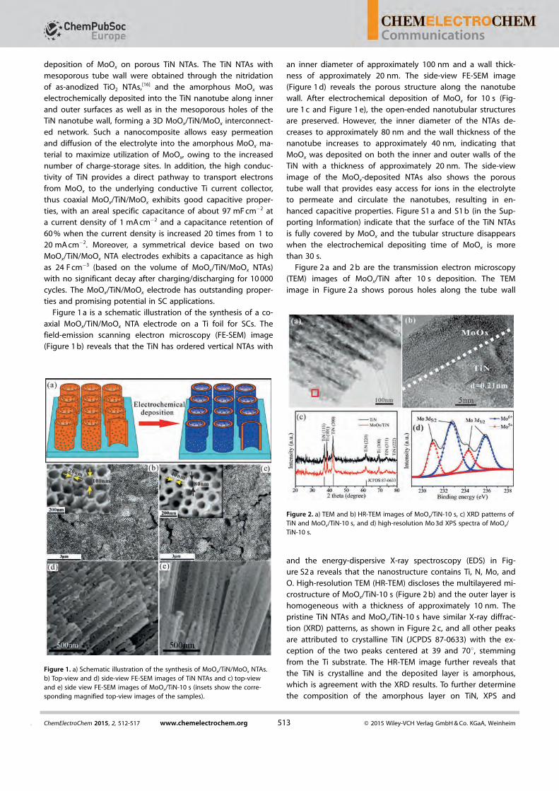
Figure 1 a is a schematic illustration of the synthesis of a co-axial MoOx/TiN/MoOx NTA electrode on a Ti foil for SCs. Thefield-emission scanning electron microscopy (FE-SEM) image(Figure 1 b) reveals that the TiN has ordered vertical NTAs with
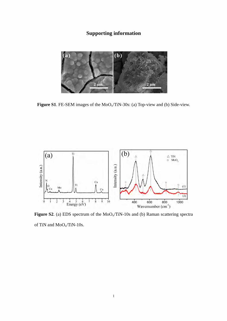
an inner diameter of approximately 100 nm and a wall thick-ness of approximately 20 nm. The side-view FE-SEM image(Figure 1 d) reveals the porous structure along the nanotubewall. After electrochemical deposition of MoOx for 10 s (Fig-ure 1 c and Figure 1 e), the open-ended nanotubular structuresare preserved. However, the inner diameter of the NTAs de-creases to approximately 80 nm and the wall thickness of thenanotube increases to approximately 40 nm, indicating thatMoOx was deposited on both the inner and outer walls of theTiN with a thickness of approximately 20 nm. The side-viewimage of the MoOx-deposited NTAs also shows the poroustube wall that provides easy access for ions in the electrolyteto permeate and circulate the nanotubes, resulting in en-hanced capacitive properties. Figure S1 a and S1 b (in the Sup-porting Information) indicate that the surface of the TiN NTAsis fully covered by MoOx and the tubular structure disappearswhen the electrochemical depositing time of MoOx is morethan 30 s.
Figure 2 a and 2 b are the transmission electron microscopy(TEM) images of MoOx/TiN after 10 s deposition. The TEMimage in Figure 2 a shows porous holes along the tube wall
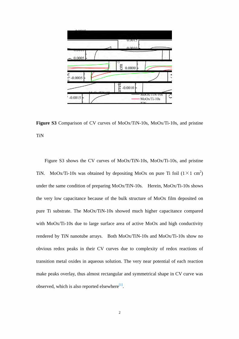
and the energy-dispersive X-ray spectroscopy (EDS) in Fig-ure S2 a reveals that the nanostructure contains Ti, N, Mo, andO. High-resolution TEM (HR-TEM) discloses the multilayered mi-crostructure of MoOx/TiN-10 s (Figure 2 b) and the outer layer ishomogeneous with a thickness of approximately 10 nm. Thepristine TiN NTAs and MoOx/TiN-10 s have similar X-ray diffrac-tion (XRD) patterns, as shown in Figure 2 c, and all other peaksare attributed to crystalline TiN (JCPDS 87-0633) with the ex-ception of the two peaks centered at 39 and 708, stemmingfrom the Ti substrate. The HR-TEM image further reveals thatthe TiN is crystalline and the deposited layer is amorphous,which is agreement with the XRD results. To further determinethe composition of the amorphous layer on TiN, XPS and
Figure 1. a) Schematic illustration of the synthesis of MoOx/TiN/MoOx NTAs.b) Top-view and d) side-view FE-SEM images of TiN NTAs and c) top-viewand e) side view FE-SEM images of MoOx/TiN-10 s (insets show the corre-sponding magnified top-view images of the samples).
Figure 2. a) TEM and b) HR-TEM images of MoOx/TiN-10 s, c) XRD patterns ofTiN and MoOx/TiN-10 s, and d) high-resolution Mo 3d XPS spectra of MoOx/TiN-10 s.
ChemElectroChem 2015, 2, 512-517 www.chemelectrochem.org � 2015 Wiley-VCH Verlag GmbH & Co. KGaA, Weinheim513&
Communications
Raman scattering were performed. Figure 2 d shows the high-resolution XPS spectrum of Mo 3d of the as-prepared MoOx/TiN-10 s. The two strong peaks at 232.8 and 235.9 eV corre-spond to Mo6+ , and two medium peaks at 231.0 and 234.3 eVarise from Mo5 + (Refs. [9a, 17]), indicating that MoOx is deposit-ed on the TiN NTAs. By calculating the area of the peaks associ-ated with Mo5+ and Mo6+ in the XPS spectra, the atomic ratioof Mo/O is calculated to be 1:2.8, suggesting the formation ofa MoO2.8 coating on both the inner and outer surfaces of theTiN nanotube. Figure S2 b shows the Raman spectra of TiN andMoOx/TiN-10 s. Compared to TiN, the Raman spectra of MoOx/TiN-10 s show additional peaks at 285 (O = Mo = O), 818 (Mo�O�Mo), and 990 cm�1 (Mo = O), which are attributed toMoOx,
[18] providing further evidence that MoOx is depositedonto the TiN NTAs.
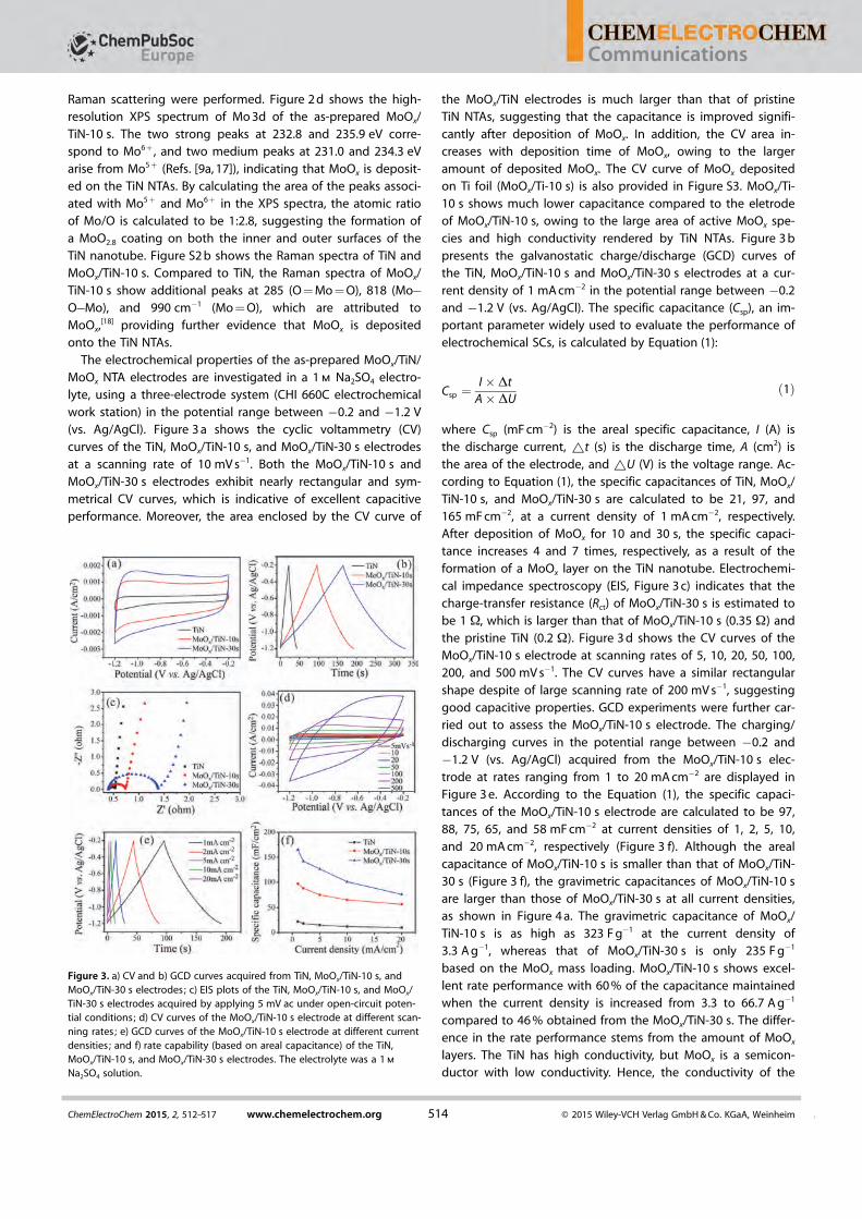
The electrochemical properties of the as-prepared MoOx/TiN/MoOx NTA electrodes are investigated in a 1 m Na2SO4 electro-lyte, using a three-electrode system (CHI 660C electrochemicalwork station) in the potential range between �0.2 and �1.2 V(vs. Ag/AgCl). Figure 3 a shows the cyclic voltammetry (CV)curves of the TiN, MoOx/TiN-10 s, and MoOx/TiN-30 s electrodesat a scanning rate of 10 mV s�1. Both the MoOx/TiN-10 s andMoOx/TiN-30 s electrodes exhibit nearly rectangular and sym-metrical CV curves, which is indicative of excellent capacitiveperformance. Moreover, the area enclosed by the CV curve of
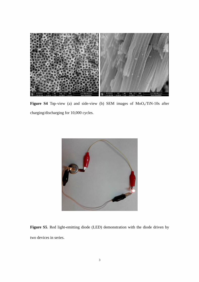
the MoOx/TiN electrodes is much larger than that of pristineTiN NTAs, suggesting that the capacitance is improved signifi-cantly after deposition of MoOx. In addition, the CV area in-creases with deposition time of MoOx, owing to the largeramount of deposited MoOx. The CV curve of MoOx depositedon Ti foil (MoOx/Ti-10 s) is also provided in Figure S3. MoOx/Ti-10 s shows much lower capacitance compared to the eletrodeof MoOx/TiN-10 s, owing to the large area of active MoOx spe-cies and high conductivity rendered by TiN NTAs. Figure 3 bpresents the galvanostatic charge/discharge (GCD) curves ofthe TiN, MoOx/TiN-10 s and MoOx/TiN-30 s electrodes at a cur-rent density of 1 mA cm�2 in the potential range between �0.2and �1.2 V (vs. Ag/AgCl). The specific capacitance (Csp), an im-portant parameter widely used to evaluate the performance ofelectrochemical SCs, is calculated by Equation (1):
Csp ¼I � Dt
A� DUð1Þ
where Csp (mF cm�2) is the areal specific capacitance, I (A) isthe discharge current, ~t (s) is the discharge time, A (cm2) isthe area of the electrode, and ~U (V) is the voltage range. Ac-cording to Equation (1), the specific capacitances of TiN, MoOx/TiN-10 s, and MoOx/TiN-30 s are calculated to be 21, 97, and165 mF cm�2, at a current density of 1 mA cm�2, respectively.After deposition of MoOx for 10 and 30 s, the specific capaci-tance increases 4 and 7 times, respectively, as a result of theformation of a MoOx layer on the TiN nanotube. Electrochemi-cal impedance spectroscopy (EIS, Figure 3 c) indicates that thecharge-transfer resistance (Rct) of MoOx/TiN-30 s is estimated tobe 1 W, which is larger than that of MoOx/TiN-10 s (0.35 W) andthe pristine TiN (0.2 W). Figure 3 d shows the CV curves of theMoOx/TiN-10 s electrode at scanning rates of 5, 10, 20, 50, 100,200, and 500 mV s�1. The CV curves have a similar rectangularshape despite of large scanning rate of 200 mV s�1, suggestinggood capacitive properties. GCD experiments were further car-ried out to assess the MoOx/TiN-10 s electrode. The charging/discharging curves in the potential range between �0.2 and�1.2 V (vs. Ag/AgCl) acquired from the MoOx/TiN-10 s elec-trode at rates ranging from 1 to 20 mA cm�2 are displayed inFigure 3 e. According to the Equation (1), the specific capaci-tances of the MoOx/TiN-10 s electrode are calculated to be 97,88, 75, 65, and 58 mF cm�2 at current densities of 1, 2, 5, 10,and 20 mA cm�2, respectively (Figure 3 f). Although the arealcapacitance of MoOx/TiN-10 s is smaller than that of MoOx/TiN-30 s (Figure 3 f), the gravimetric capacitances of MoOx/TiN-10 sare larger than those of MoOx/TiN-30 s at all current densities,as shown in Figure 4 a. The gravimetric capacitance of MoOx/TiN-10 s is as high as 323 F g�1 at the current density of3.3 A g�1, whereas that of MoOx/TiN-30 s is only 235 F g�1
based on the MoOx mass loading. MoOx/TiN-10 s shows excel-lent rate performance with 60 % of the capacitance maintainedwhen the current density is increased from 3.3 to 66.7 A g�1
compared to 46 % obtained from the MoOx/TiN-30 s. The differ-ence in the rate performance stems from the amount of MoOx
layers. The TiN has high conductivity, but MoOx is a semicon-ductor with low conductivity. Hence, the conductivity of the
Figure 3. a) CV and b) GCD curves acquired from TiN, MoOx/TiN-10 s, andMoOx/TiN-30 s electrodes; c) EIS plots of the TiN, MoOx/TiN-10 s, and MoOx/TiN-30 s electrodes acquired by applying 5 mV ac under open-circuit poten-tial conditions; d) CV curves of the MoOx/TiN-10 s electrode at different scan-ning rates; e) GCD curves of the MoOx/TiN-10 s electrode at different currentdensities; and f) rate capability (based on areal capacitance) of the TiN,MoOx/TiN-10 s, and MoOx/TiN-30 s electrodes. The electrolyte was a 1 m
Na2SO4 solution.
ChemElectroChem 2015, 2, 512–517 www.chemelectrochem.org � 2015 Wiley-VCH Verlag GmbH & Co. KGaA, Weinheim514 &
Communications
MoOx/TiN nanocomposite electrode drops after more MoOx
deposition, as suggested by the EIS results in Figure 3 c. In fact,the larger the amount of MoOx loaded, the lower the conduc-tivity. Our results reveal a special feature of MoOx deposited onhighly conductive TiN NTAs, which can be charged/dischargedat a high current density of approximately 70 A g�1 with anareal capacitance of 58 mF cm�2 (gravimetric capacitance193 F g�1), which is much bigger than the values observedfrom many other TMO-based electrodes, such as b-MnO2 nano-rod@nanoflake (Ni, Co, Mn) oxides,[19] g-FeOOH nanosheets,[20]
MoO3 nanobelts,[21] and Co3O4/Co3(VO4)2 hybrid nanorods.[22]
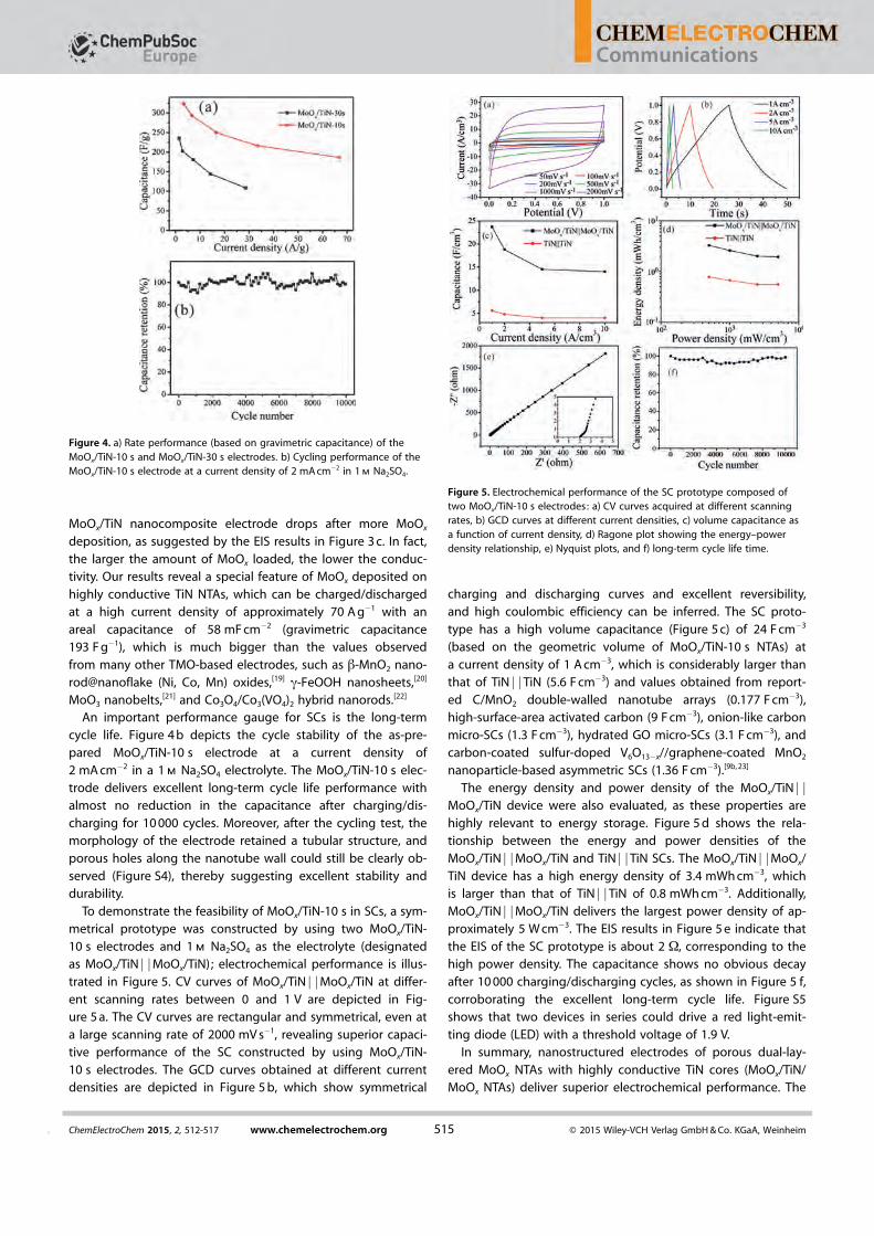
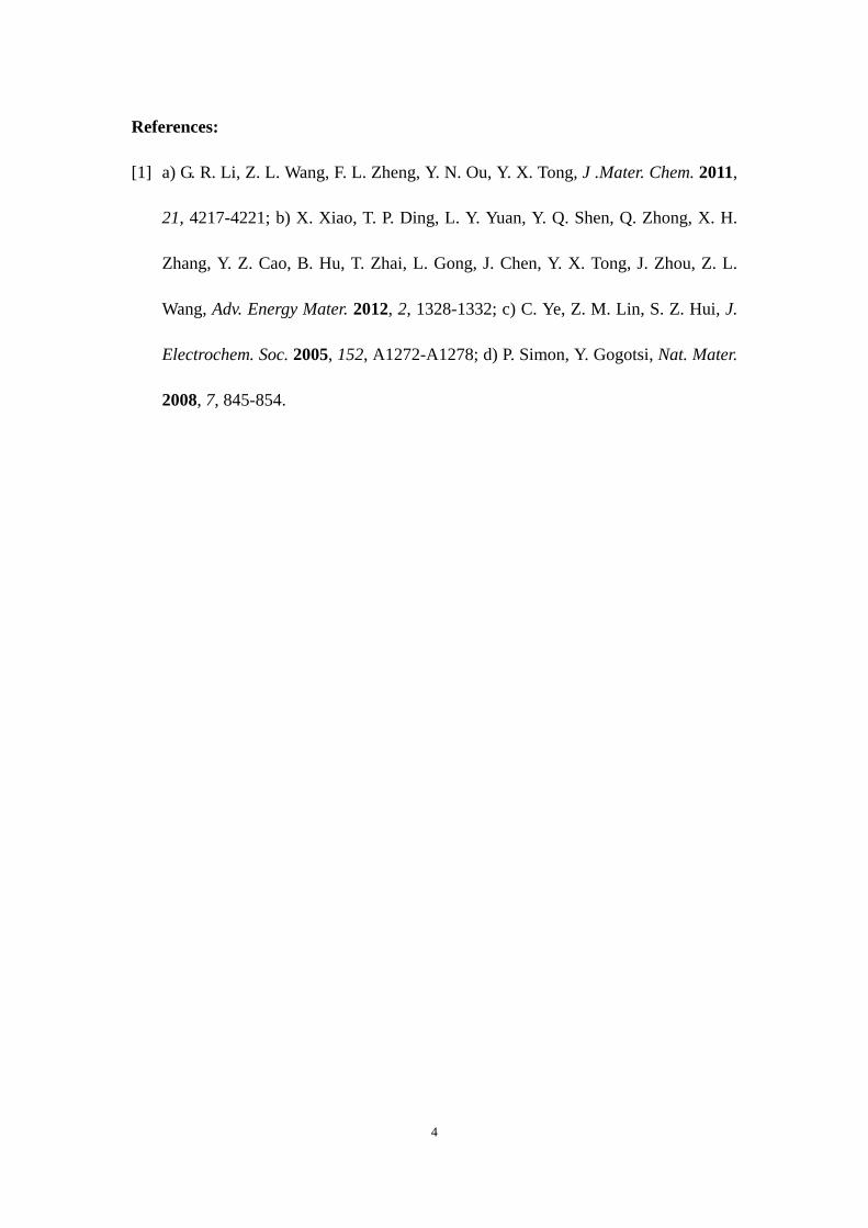
An important performance gauge for SCs is the long-termcycle life. Figure 4 b depicts the cycle stability of the as-pre-pared MoOx/TiN-10 s electrode at a current density of2 mA cm�2 in a 1 m Na2SO4 electrolyte. The MoOx/TiN-10 s elec-trode delivers excellent long-term cycle life performance withalmost no reduction in the capacitance after charging/dis-charging for 10 000 cycles. Moreover, after the cycling test, themorphology of the electrode retained a tubular structure, andporous holes along the nanotube wall could still be clearly ob-served (Figure S4), thereby suggesting excellent stability anddurability.
To demonstrate the feasibility of MoOx/TiN-10 s in SCs, a sym-metrical prototype was constructed by using two MoOx/TiN-10 s electrodes and 1 m Na2SO4 as the electrolyte (designatedas MoOx/TiN j jMoOx/TiN); electrochemical performance is illus-trated in Figure 5. CV curves of MoOx/TiN j jMoOx/TiN at differ-ent scanning rates between 0 and 1 V are depicted in Fig-ure 5 a. The CV curves are rectangular and symmetrical, even ata large scanning rate of 2000 mV s�1, revealing superior capaci-tive performance of the SC constructed by using MoOx/TiN-10 s electrodes. The GCD curves obtained at different currentdensities are depicted in Figure 5 b, which show symmetrical
charging and discharging curves and excellent reversibility,and high coulombic efficiency can be inferred. The SC proto-type has a high volume capacitance (Figure 5 c) of 24 F cm�3
(based on the geometric volume of MoOx/TiN-10 s NTAs) ata current density of 1 A cm�3, which is considerably larger thanthat of TiN j jTiN (5.6 F cm�3) and values obtained from report-ed C/MnO2 double-walled nanotube arrays (0.177 F cm�3),high-surface-area activated carbon (9 F cm�3), onion-like carbonmicro-SCs (1.3 F cm�3), hydrated GO micro-SCs (3.1 F cm�3), andcarbon-coated sulfur-doped V6O13�x//graphene-coated MnO2
nanoparticle-based asymmetric SCs (1.36 F cm�3).[9b, 23]
The energy density and power density of the MoOx/TiN j jMoOx/TiN device were also evaluated, as these properties arehighly relevant to energy storage. Figure 5 d shows the rela-tionship between the energy and power densities of theMoOx/TiN j jMoOx/TiN and TiN j jTiN SCs. The MoOx/TiN j jMoOx/TiN device has a high energy density of 3.4 mWh cm�3, whichis larger than that of TiN j jTiN of 0.8 mWh cm�3. Additionally,MoOx/TiN j jMoOx/TiN delivers the largest power density of ap-proximately 5 W cm�3. The EIS results in Figure 5 e indicate thatthe EIS of the SC prototype is about 2 W, corresponding to thehigh power density. The capacitance shows no obvious decayafter 10 000 charging/discharging cycles, as shown in Figure 5 f,corroborating the excellent long-term cycle life. Figure S5shows that two devices in series could drive a red light-emit-ting diode (LED) with a threshold voltage of 1.9 V.
In summary, nanostructured electrodes of porous dual-lay-ered MoOx NTAs with highly conductive TiN cores (MoOx/TiN/MoOx NTAs) deliver superior electrochemical performance. The
Figure 4. a) Rate performance (based on gravimetric capacitance) of theMoOx/TiN-10 s and MoOx/TiN-30 s electrodes. b) Cycling performance of theMoOx/TiN-10 s electrode at a current density of 2 mA cm�2 in 1 m Na2SO4.
Figure 5. Electrochemical performance of the SC prototype composed oftwo MoOx/TiN-10 s electrodes: a) CV curves acquired at different scanningrates, b) GCD curves at different current densities, c) volume capacitance asa function of current density, d) Ragone plot showing the energy–powerdensity relationship, e) Nyquist plots, and f) long-term cycle life time.
ChemElectroChem 2015, 2, 512-517 www.chemelectrochem.org � 2015 Wiley-VCH Verlag GmbH & Co. KGaA, Weinheim515&
Communications

areal specific capacitance of theh MoOx/TiN/MoOx NTA elec-trode increases up to four times compared to the pristine TiNelectrode and 60 % is retained when the current density is in-creased 20 times (from 1 to 20 mA cm�2). After cycling 10 000times, no significant decay in the capacitance is observed. TheSC prototype constructed with MoOx/TiN-10 s exhibits a largecapacitance of 24 F cm�3, which does not degrade after 10 000charging/discharging cycles. The excellent performance deliv-ered by the MoOx/TiN-10 s electrode can be attributed to the3D interconnected network and highly conductive core, andthe materials have large potential in energy-storage devices.
Experimental Section
The TiN NTAs were prepared according previously described proce-dures.[16] The TiO2 NTAs were prepared through electrochemicalanodization of Ti foils (Goodfellow, 10 � 10 � 0.1 mm3), which wascut by using a wire-electrode-cutting machine and measured againwith a Vernier caliper. Anodization was carried out in a conventionaltwo-electrode cell equipped with a direct current (DC) powersupply (IT6834, ITECH, China) at 60 V for 4 h at room temperature(RT). The Ti foil served as the anode and a graphite foil was thecounter electrode (1 cm separation). The electrolyte was ethyleneglycol containing 0.5 wt % ammonium fluoride, 5 vol % doubly dis-tilled water, and 5 vol % methanol. The as-anodized TiO2 NTAs weregrown in situ on Ti foil, which were annealed at 450 8C in air for3 h (designated as TiO2) to convert into the anatase phase, fol-lowed by thermal treatment in NH3 at 800 8C for 3 h to form theTiN NTAs. The MoOx/TiN nanocomposite was produced throughelectrochemical deposition of MoOx on TiN NTAs in a solution con-taining 0.1 m Na2MoO4, 0.1 m Na2EDTA, and 0.1 m CH3COONH4 andpotentiostatic electrolysis was performed at �2.0 V and 70 8C witha Ag/AgCl electrode as the reference electrode and Pt foil (2 �2 cm2) as the counter electrode for 10 and 30 s (designated asMoOx/TiN-10 s and MoOx/TiN-30 s, respectively). The mass loadingof MoO3 for MoOx/TiN-10 s and MoOx/TiN-30 s was measured to be0.3 and 0.7 mg cm�2, respectively, according to the mass changebefore and after electrochemical deposition by using a high-preci-sion electronic microbalance.
The samples were characterized by using FE-SEM (FEI Nova 450Nano), HR-TEM (Tecnai G2 U-TWIN), EDS, XRD (Philips X’ Pert Pro)with CuKa radiation (1.5418 �) in the range of 20–808 (2q), XPS(ESCALB MK-II, VG Instruments, U. K.), and micro-Raman scatteringat RT (HR RamLab with the 514.5 nm Ar+ laser as the excitationsource).
The electrochemical measurements were conducted on a CHI 660Cinstrument. The three-electrode cell consisted of a Ag/AgCl elec-trode as the reference electrode, platinum plate as the counterelectrode, and MoOx/TiN/MoOx as the working electrode. 1 m
Na2SO4 aqueous solution was used as the electrolyte. CV was per-formed between �0.2 and �1.2 V (vs. Ag/AgCl) at different scan-ning rates and the GCD curves were acquired at different currentdensities in the voltage range between �0.2 and �1.2 V (vs. Ag/AgCl). EIS was performed at the open-circuit potential with an acperturbation voltage of 5 mV and the cycling stability was assessedon a charge/discharge tester (Land CT2001 A, Wuhan LAND Elec-tronics Co., Ltd. , China). A symmetrical prototype based on twopieces of MoOx/TiN-10 s was assembled in a 2032-type stainless-steel coin cell. In detail, two of MoOx/TiN-10 s electrodes wereplaced at the opposite sides of the separator (NKK TF40) with theMoOx/TiN-10 s side towards the separator. Then, several drops of
1 m Na2SO4 electrolyte were added and sealed by using a button-cell sealing machine with a press of 10 Mpa. The cycling per-formance was tested on a two-electrode battery test system (LandCT2001 A). The CV, GCD, and EIS measurements were performedon an electrochemical workstation (CHI 660C).
Acknowledgements
This work was financially supported by the National Natural Sci-ence Foundation of China (Grant No. 50902104 and 21105077),Fundamental Research Funds for the Central Universities (HUST:0118187030), Outstanding Young and Middle-aged Scientific In-novation Team of Colleges and Universities of Hubei Province(T201402) and City University of Hong Kong Applied ResearchGrant (ARG) No. 9667085. The authors also thank the facility sup-port of the Center for Nanoscale Characterization & Devices(CNCD), WNLO-HUST, and the Analysis and Testing Center ofHuazhong University of Science and Technology.
Keywords: conductive core · electrochemistry · energyconversion · molybdenum · TiN nanotube arrays
[1] a) P. Simon, Y. Gogotsi, Nat. Mater. 2008, 7, 845 – 854; b) A. L. M. Reddy,M. M. Shaijumon, S. R. Gowda, P. M. Ajayan, J. Phys. Chem. C 2010, 114,658 – 663; c) B. E. Conway, Electrochemical Capacitors: Scientific Funda-mentals and Technological Applications, Kluwer Academic/Plenum,London, 1999.
[2] a) L. L. Zhang, X. Zhao, Chem. Soc. Rev. 2009, 38, 2520 – 2531; b) W. Wei,X. Cui, W. Chen, D. G. Ivey, Chem. Soc. Rev. 2011, 40, 1697 – 1721.
[3] a) J. Rajeswari, P. S. Kishore, B. Viswanathan, T. K. Varadarajan, Electro-chem. Commun. 2009, 11, 572 – 575; b) D. A. Tompsett, S. C. Parker, M. S.Islam, J. Mater. Chem. A 2014, 2, 15509 – 15518.
[4] a) H. Y. Lee, J. B. Goodenough, J. Solid State Chem. 1999, 148, 81 – 84;b) H. Wang, H. Yi, X. Chen, X. Wang, J. Mater. Chem. A 2014, 2, 1165 –1173.
[5] a) J. Mu, B. Chen, Z. Guo, M. Zhang, Z. Zhang, P. Zhang, C. Shao, Y. Liu,Nanoscale 2011, 3, 5034 – 5040; b) S. Sun, J. Lang, R. Wang, L. Kong, X.Li, X. Yan, J. Mater. Chem. A 2014, 2, 14550 – 14556.
[6] a) G. Abell�n, E. Coronado, C. Mart�-Gastaldo, A. Ribera, T. F. Otero, Part.Part. Syst. Charact. 2013, 30, 853 – 863; b) Q. Lu, M. W. Lattanzi, Y. Chen,X. Kou, W. Li, X. Fan, K. M. Unruh, J. G. Chen, J. Q. Xiao, Angew. Chem.Int. Ed. 2011, 50, 6847 – 6850; Angew. Chem. 2011, 123, 6979 – 6982;c) G. P. Wang, L. Zhang, J. J. Zhang, Chem. Soc. Rev. 2012, 41, 797 – 828.
[7] a) C. Zhou, Y. Zhang, Y. Li, J. Liu, Nano Lett. 2013, 13, 2078 – 2085; b) C.Guan, J. Liu, C. Cheng, H. Li, X. Li, W. Zhou, H. Zhang, H. J. Fan, EnergyEnviron. Sci. 2011, 4, 4496 – 4499.
[8] a) J. Jiang, J. Liu, S. Peng, D. Qian, D. Luo, Q. Wang, Z. Tian, Y. Liu, J.Mater. Chem. A 2013, 1, 2588; b) I. Shakir, M. Shahid, U. A. Rana, M. F.Warsi, RSC Adv. 2014, 4, 8741 – 8745.
[9] a) S. D. Perera, B. Patel, N. Nijem, K. Roodenko, O. Seitz, J. P. Ferraris, Y. J.Chabal, K. J. Balkus, Adv. Energy Mater. 2011, 1, 936 – 945; b) T. Zhai, X.Lu, Y. Ling, M. Yu, G. Wang, T. Liu, C. Liang, Y. Tong, Y. Li, Adv. Mater.2014, 26, 5869 – 5875.
[10] M. E. Spahr, P. Nov�k, O. Haas, R. Nesper, J. Power Sources 1995, 54,346 – 351.
[11] a) G. R. Li, Z. L. Wang, F. L. Zheng, Y. N. Ou, Y. X. Tong, J. Mater. Chem.2011, 21, 4217 – 4221; b) W. Tang, L. Liu, S. Tian, L. Li, Y. Yue, Y. Wu, K.Zhu, Chem. Commun. 2011, 47, 10058 – 10060; c) T. Brezesinski, J. Wang,S. H. Tolbert, B. Dunn, Nat. Mater. 2010, 9, 146 – 151.
[12] a) H. Zhang, G. Cao, Z. Wang, Y. Yang, Z. Shi, Z. Gu, Nano Lett. 2008, 8,2664 – 2668; b) S. Devaraj, N. Munichandraiah, J. Phys. Chem. C 2008,112, 4406 – 4417; c) L. Mao, K. Zhang, H. S. O. Chan, J. S. Wu, J. Mater.Chem. 2012, 22, 1845 – 1851; d) H. B. Li, M. H. Yu, F. X. Wang, P. Liu, Y.Liang, J. Xiao, C. X. Wang, Y. X. Tong, G. W. Yang, Nat. Commun. 2013, 4,1894.
ChemElectroChem 2015, 2, 512-517 www.chemelectrochem.org � 2015 Wiley-VCH Verlag GmbH & Co. KGaA, Weinheim516 &
Communications
[13] a) J. Liu, J. Essner, J. Li, Chem. Mater. 2010, 22, 5022 – 5030; b) J. Chang,M. Jin, F. Yao, T. H. Kim, V. T. Le, H. Yue, F. Gunes, B. Li, A. Ghosh, S. Xie,Adv. Funct. Mater. 2013, 23, 5074 – 5083; c) L. Noerochim, J.-Z. Wang, D.Wexler, Z. Chao, H.-K. Liu, J. Power Sources 2013, 228, 198 – 205.
[14] a) L. S. Aravinda, K. K. Nagaraja, K. U. Bhat, B. R. Bhat, J. Electroanal.Chem. 2013, 699, 28 – 32; b) G. B. Wang, J. F. Ni, H. B. Wang, L. J. Gao, J.Mater. Chem. A 2013, 1, 4112 – 4118; c) S. Okashy, M. Noked, T. Zimrin,D. Aurbach, J. Electrochem. Soc. 2013, 160, A1489 – A1496; d) X. Xiao,T. P. Ding, L. Y. Yuan, Y. Q. Shen, Q. Zhong, X. H. Zhang, Y. Z. Cao, B. Hu,T. Zhai, L. Gong, J. Chen, Y. X. Tong, J. Zhou, Z. L. Wang, Adv. EnergyMater. 2012, 2, 1328 – 1332.
[15] Z. N. Yu, B. Duong, D. Abbitt, J. Thomas, Adv. Mater. 2013, 25, 3302 –3306.
[16] X. Peng, K. Huo, J. Fu, X. Zhang, B. Gao, P. K. Chu, Chem. Commun.2013, 49, 10172 – 10174.
[17] D. Xiang, C. Han, J. L. Zhang, W. Chen, Sci. Rep. 2014, 4, 4891.[18] a) E. D. B. Santos, J. M. De Souza, E. Silva, I. O. Mazali, Mater. Res. Bull.
2010, 45, 1707 – 1712; b) L. Seguin, M. Figlarz, R. Cavagnat, J.-C. Lass�-gues, Spectrochim. Acta A 1995, 51, 1323 – 1344; c) B. Chae, Y. M. Jung,X. Wu, S. B. Kim, J. Raman Spectrosc. 2003, 34, 451 – 458.
[19] H. Wang, Q. Zhao, X. Wang, Y. Zhang, J. Gao, Y. Fu, X. Yang, H. Shu, RSCAdv. 2014, 4, 42910 – 42916.
[20] Y. C. Chen, Y. G. Lin, Y. K. Hsu, S. C. Yen, K. H. Chen, L. C. Chen, Small2014, 10, 3803 – 3810.
[21] H. Peng, G. F. Ma, J. J. Mu, K. J. Sun, Z. Q. Lei, J. Mater. Chem. A 2014, 2,10384 – 10388.
[22] W. B. Zhang, L. B. Kong, X. J. Ma, Y. C. Luo, L. Kang, J. Power Sources2014, 269, 61 – 68.
[23] a) Q. Li, X. F. Lu, H. Xu, Y. X. Tong, G. R. Li, ACS Appl. Mater. Interfaces2014, 6, 2726 – 2733; b) D. Pech, M. Brunet, H. Durou, P. H. Huang, V.Mochalin, Y. Gogotsi, P. L. Taberna, P. Simon, Nat. Nanotechnol. 2010, 5,651 – 654; c) W. Gao, N. Singh, L. Song, Z. Liu, A. L. M. Reddy, L. J. Ci, R.Vajtai, Q. Zhang, B. Q. Wei, P. M. Ajayan, Nat. Nanotechnol. 2011, 6, 496 –500.
Received: October 16, 2014
Revised: November 10, 2014
Published online on
ChemElectroChem 2015, 2, 512-517 www.chemelectrochem.org � 2015 Wiley-VCH Verlag GmbH & Co. KGaA, Weinheim517&
Communications
December
: December 23, 2014
Supporting Information
Porous Dual-Layered MoOx Nanotube Arrays with HighlyConductive TiN Cores for SupercapacitorsXiang Peng,[a, c] Kaifu Huo,*[a] Jijiang Fu,[b] Biao Gao,[b] Lei Wang,[a] Liangsheng Hu,[b, c]
Xuming Zhang,[c] and Paul K. Chu[c]
celc_201402349_sm_miscellaneous_information.pdf
1
Supporting information
Figure S1. FE-SEM images of the MoOx/TiN-30s: (a) Top-view and (b) Side-view.
Figure S2. (a) EDS spectrum of the MoOx/TiN-10s and (b) Raman scattering spectra
of TiN and MoOx/TiN-10s.
2 μm
( a )
2 μm
( b )
2
Figure S3 Comparison of CV curves of MoOx/TiN-10s, MoOx/Ti-10s, and pristine
TiN
Figure S3 shows the CV curves of MoOx/TiN-10s, MoOx/Ti-10s, and pristine
TiN. MoOx/Ti-10s was obtained by depositing MoOx on pure Ti foil (1×1 cm2)
under the same condition of preparing MoOx/TiN-10s. Herein, MoOx/Ti-10s shows
the very low capacitance because of the bulk structure of MoOx film deposited on
pure Ti substrate. The MoOx/TiN-10s showed much higher capacitance compared
with MoOx/Ti-10s due to large surface area of active MoOx and high conductivity
rendered by TiN nanotube arrays. Both MoOx/TiN-10s and MoOx/Ti-10s show no
obvious redox peaks in their CV curves due to complexity of redox reactions of
transition metal oxides in aqueous solution. The very near potential of each reaction
make peaks overlay, thus almost rectangular and symmetrical shape in CV curve was
observed, which is also reported elsewhere[1].
3
Figure S4 Top-view (a) and side-view (b) SEM images of MoOx/TiN-10s after
charging/discharging for 10,000 cycles.
Figure S5. Red light-emitting diode (LED) demonstration with the diode driven by
two devices in series.
4
References:
[1] a) G. R. Li, Z. L. Wang, F. L. Zheng, Y. N. Ou, Y. X. Tong, J .Mater. Chem. 2011,
21, 4217-4221; b) X. Xiao, T. P. Ding, L. Y. Yuan, Y. Q. Shen, Q. Zhong, X. H.
Zhang, Y. Z. Cao, B. Hu, T. Zhai, L. Gong, J. Chen, Y. X. Tong, J. Zhou, Z. L.
Wang, Adv. Energy Mater. 2012, 2, 1328-1332; c) C. Ye, Z. M. Lin, S. Z. Hui, J.
Electrochem. Soc. 2005, 152, A1272-A1278; d) P. Simon, Y. Gogotsi, Nat. Mater.
2008, 7, 845-854.