
Strontium ranelate improves bone strength in ovariectomized ...
FULL P
APER
© 2014 WILEY-VCH Verlag GmbH & Co. KGaA, Weinheim 6783wileyonlinelibrary.com
1. Introduction
Among different crystal structures and morphologies of TiO 2 , vertically oriented anatase nanotube arrays show the highest activity for solar energy conversion. [ 1,2 ] However, the long-standing bottleneck is the fact that TiO 2 is a wide band gap semi-conductor, limiting its activation to the deep-blue and ultraviolet spectral region that contains but a small fraction (5%) of the incident solar energy. [ 3 ] Therefore, a plethora of strategies have been developed to improve the photoresponse of such material. Composite TiO 2 nanotube arrays (hereafter named TiO 2 NTAs) in so-called sandwich structures, core–shell geometry or decorated with nanoparticles have been shown to be promising photocatalysts due to the improvement of charge carrier separation. Among those strategies, dye-sensitization and band gap engineering via doping are considered the most prom-ising routes to pursue. [ 4,5 ] For example, aliovalent metal ion doping was shown to introduce mid-gap energy levels, which
are expected to control the band gap response of the nanotube arrays and enhance their visible spectrum properties. [ 2,6,7 ] How-ever, the developed various doping approaches suffer from mul-tiple, tedious steps, which often result in poor structural and morphological control. Consequently, there is a lot of debate whether the observed enhancement in the optical/photoelectro-chemical properties of the doped material is due to the dopants or the artifacts associated with the doping process. [ 7 ] Another major challenge in the analysis of doping mechanism is the ability to detect the dopant, which is usually an extremely small fraction in the host material.
SrTiO 3 has been intensively investigated as a photoanode for water splitting due to its high corrosion resistance, excel-lent photocatalytic activity, high stability, and non-toxicity. [ 8–10 ] Despite the wide band gap of SrTiO 3 (3.2 eV), the band edges are properly positioned with respect to both oxygen and hydrogen redox potentials. Recently, the electrode system of SrTiO 3 /TiO 2 nanotube arrays is reported as an effi cient photo catalyst for hydrogen production under visible irradiation compared with pure TiO 2 . [ 11 ] However, the improved photoelectrochemical
An Experimental Insight into the Structural and Electronic Characteristics of Strontium-Doped Titanium Dioxide Nanotube Arrays
Hoda Amani Hamedani , * Nageh K. Allam , Mostafa A. El-Sayed , Mohammad A. Khaleel , Hamid Garmestani , and Faisal M. Alamgir
The possibility of in situ doping during electrochemical anodization of titania nanotube arrays is demonstrated and the mechanism and variations in struc-tural and electronic characteristics of the nanotube arrays as after doping is systematically explored. In the presence of strontium as the dopant, bulk analysis shows strontium mainly incorporated into the lattice of TiO 2 . Surface analysis, however, reveals phase segregation of SrO in the TiO 2 matrix at high Sr doping levels. The near edge X-ray absorption fi ne structure (NEXAFS) spectroscopy analysis reveals that Sr 2+ doping only alters the Ti and O ions interaction in the TiO 2 lattice on the surface with no effect on their individual charge states. An in-depth understanding of the dopant incorporation mecha-nism and distribution into TiO 2 nanotube arrays is achieved using high reso-lution transmission electron microscopy (HRTEM) and the high angle annular dark-fi eld scanning transmission electron microscopy (HAADF-STEM) cou-pled with the electron energy loss spectroscopy (EELS) measurements on the surface and bulk of the nanotubes. Upon their use to photoelectrochemically split water, the Sr-doped TiO 2 nanotube fi lm shows incident photon conver-sion effi ciencies (IPCE) as high as 65%. The enhanced light activity in con-junction with the ordered one-dimensional morphology makes the fabricated fi lms promising candidates for water photoelectrolysis.
DOI: 10.1002/adfm.201401760
H. Amani Hamedani, H. Garmestani, F. M. Alamgir School of Materials Science and Engineering Georgia Institute of Technology Atlanta , GA 30332 , USA E-mail: [email protected] N. K. Allam Energy Materials Laboratory (EML) Physics Department School of Sciences and Engineering The American University in Cairo New Cairo 11835 , Egypt M. A. El-Sayed School of Chemistry and Biochemistry Georgia Institute of Technology Atlanta , GA 30332 , USA M. A. Khaleel Qatar Energy and Environment Research Institute Qatar Foundation P.O. Box 5825 , Doha , Qatar
Adv. Funct. Mater. 2014, 24, 6783–6796
www.afm-journal.dewww.MaterialsViews.com
FULL
PAPER
6784 wileyonlinelibrary.com © 2014 WILEY-VCH Verlag GmbH & Co. KGaA, Weinheim
performance of such composite system is shown to be strongly dependent on the dispersion of SrTiO 3 nanocrystallites on TiO 2 nanotube arrays. Considering the advantages of doping and decoration approaches on the improvement of band gap structure in TiO 2 nanotube arrays, it would be more desirable to incorporate metal ions into the TiO 2 nanotube arrays during their fabrication. As such, band gap engineering of the TiO 2 nanotubes with Sr was implemented in our previous study by in situ doping, as an alternative strategy to avoid such structural imperfections and morphological defects imposed by multi-steps fabrication methods. The electrodes composed of these Sr-doped TiO 2 nanotube arrays in the aforementioned study have shown a signifi cant enhancement in the photoconversion effi ciency for electrochemical water splitting. [ 12 ]
Here we demonstrate a systematic approach to explore the doping mechanism as well as the induced nanostructural changes/defects in the bulk and surface structure of Sr-doped TiO 2 nanotube arrays synthesized via one step in situ doping during anodization. Detailed bulk and surface analyses of the Sr-doped TiO 2 nanotube arrays is made using state-of-the art sur-face sensitive and spectroscopic characterization techniques such as Glancing incidence X-ray diffraction (GIXRD), X-ray photo-electron spectroscopy (XPS), and near edge X-ray absorption fi ne structure (NEXAFS) spectroscopy. Furthermore, the use of fi eld emission scanning electron microscopy (FESEM) and atomic resolution transmission electron microscopy (TEM) on a single TiO 2 nanotube has enabled reliable identifi cation of success or failure of doping, the uniformity of doping along the nanotube length and in the radial direction of a nanotube as well as the mechanism involved. The results obtained in this work provide an important insight into the in situ doping mechanism of alio-valent ions in self-assembled TiO 2 nanotube arrays. In addition, it offers a critical depth of understanding towards realization of the effect of doping on photoelectrochemical water splitting per-formance of the TiO 2 as well as other material systems.
2. Results and Discussion
2.1. Morphology and Crystallinity of Undoped and Strontium-Doped TiO 2 NTAs
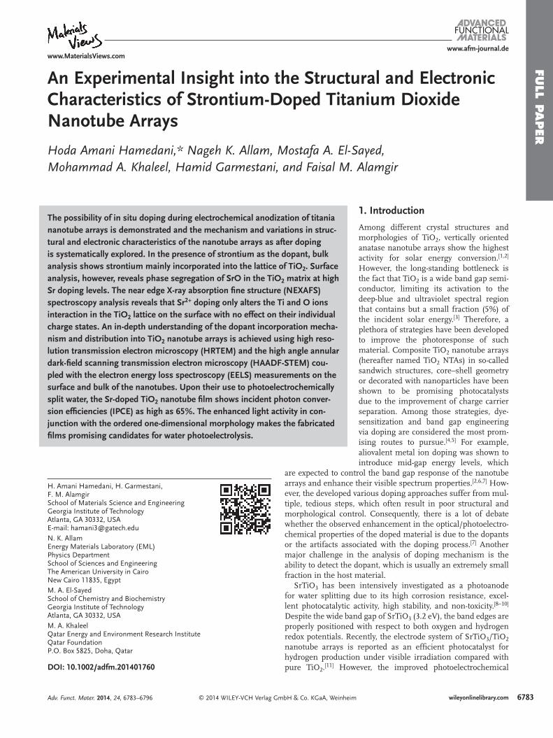
Figure 1 a shows typical cross-section view FESEM image of the annealed Sr-doped TiO 2 nanotubes grown in an electrolyte
containing 0.04 M Sr(OH) 2 at 20 V for 3 h. The surface mor-phology of the nanotubes with tube diameter of 100 ± 10 nm was found to be unchanged after doping. More details on the fabrication process and characterization of the resulting nano-tubes can be found in our recent publication. [ 12 ] The Sr content was estimated using ICP MS and XPS analyses (Table S1, Sup-porting Information). The crystallization temperature remains the same in the Sr-doped Ti oxide nanotubes compared to that of the undoped counterparts. This is in contrast to Low et al.’s observation where Cr-doping has lowered the crystal-lization temperature of anatase from 600 to 400 °C and rutile from 600 to 500 °C. [ 5 ] The phase transformation from anatase to rutile in undoped Ti oxide nanotubes usually occurs between 300-600 °C. However, the phase transformation from anatase to rutile in the Sr-doped Ti oxide nanotubes in our work was always observed around 600 °C as seen in the HT-XRD patterns in Figure S1 in the Supporting Information. This is also in con-trast to their fi ndings where Cr-doping has dramatically reduced the fraction of anatase-to-rutile transformation. In our work, the rutile phase was also seen to be stable when the sample was cooled down to room temperature (25 °C) as seen below.
2.2. Effect of Dopant on the Lattice and Defect Structure of TiO 2 NTAs
Figure 1 b,c show a typical cross-sectional view TEM image, the EDS spectrum and the corresponding EDS map of a single Sr-doped TiO 2 nanotube along the longitudinal direction. The EDS spectrum reveals the presence of Ti K and Sr L peaks in the doped sample. Also, the EDS Sr L map, extracted based on Sr L line, reveals a homogenous distribution of Sr along the length of the selected single tube.
Figure 2 shows a high resolution TEM view of a single annealed Sr-doped nanotube with the corresponding diffraction pattern shown in the inset (Figure 2 a). The crystallinity of the nanotube is confi rmed where the bulk is composed of a crys-talline region in the middle with clear lattice fringes. The ori-entation of the crystals is clearly observed from the diffraction pattern of the middle region with the majority (101) oriented planes observed from the indexing of the fast Fourier transform (FFT) as shown in the inset in Figure 2 b. The HRTEM image and the FFT reconstructed image in the inset of Figure 2 c show a d -spacing of 0.35 nm, which corresponds to (101) planes.
Adv. Funct. Mater. 2014, 24, 6783–6796
www.afm-journal.dewww.MaterialsViews.com
Figure 1. Cross-sectional view a) FESEM and b) TEM images of annealed Sr-doped nanotubes (ST2). c) EDS spectrum and the corresponding EDS map of the selected single nanotube along the longitudinal direction.

FULL P
APER
6785wileyonlinelibrary.com© 2014 WILEY-VCH Verlag GmbH & Co. KGaA, Weinheim
However, the crystalline region is encompassed with a fairly thick (≈15 nm) amorphous layer that extends over the entire length of the nanotube. This amorphous layer is thicker than that typically seen in undoped TiO 2 nanotubes (Figure 2 d,e).
Figure 3 a shows the GIXRD patterns of the annealed undoped and Sr-doped TiO 2 nanotube arrays prepared in elec-trolytes with three different dopant concentrations at pH = 3. All patterns confi rm the formation of anatase phase, which crystallizes within the I4 1 /amd space group (tetragonal cell). No evidence for new phase formation upon doping was found from the GIXRD patterns. Note that the peak position of tita-nium at 2 θ = 40.5° was considered as the reference position for comparison of the undoped and doped TiO 2 samples. From the variation in the intensity of the (004) peak with increasing the dopant content, it was observed that the intensity is increased from undoped sample to ST2. However, a sudden change occurs in the highest doped sample (ST3). As the (004) refl ec-tion is related to changes in dimension along the c-axis, it appears that the lattice has slightly distorted along the c-axis in the ST3 sample.
In general, as the dopant content increases, a gradual shift in the lattice parameters of the host material is observed due to the induced strain upon the incorporation of the dopant into the periodic crystal lattice. According to Vegard’s law, the average lattice parameter varies linearly with dopant concentra-tion in the crystal, and typically the deviations from linearity are indications of phase transitions or segregation. [ 13 ] Note that the anatase (101) peak is shifted towards smaller 2 θ values with increasing the Sr concentration as observed in the close-up view of the (101) as shown in the inset. This shift can be attributed to the incorporation of the Sr 2+ , with larger ionic radius (1.18 Å) than that of Ti 4+ (0.605Å), into the crystal lattice of TiO 2 . As the concentration of the dopant increases, it is expected that more Sr 2+ ions are incorporated into the TiO 2 crystal lattice and as a result the corresponding peaks are more shifted to the lower
angle side. In order to investigate the reproducibility of the GIXRD measurements, Table 1 shows the two-theta peak posi-tions corresponding to (101) and (004) planes that are obtained from repeated GIXRD experiments on all samples.
Based on Scherrer’s formula, peak broadening is essentially associated with crystallite size and non-uniform strain (micro-strain) due to shifts of atoms from their ideal positions. The crystallite sizes of the undoped and doped samples, calculated using Scherrer's formula, were found to be similar and in the range of 25 nm to 35 nm. The change in the d -spacing in (101), (103), (004), and (200) planes in doped samples is cal-culated from Bragg’s law and shown as a function of dopant concentration in Figure 3 b. The main source of error in the lattice parameters calculations, for X-Ray diffractometers with Bragg-Brentano geometry, is related to the alignment of instru-ment (zero 2-theta offset and peak position). [ 14 ] This effect is taken into account in our measurements by alignment of the instrument before performing the scans and by using the Ti peak corresponding to the metallic titanium in the substrate as the reference peak for all samples. The accuracy of the meas-urements was also determined based on the instrument preci-sion of 0.02° measurement for the 2-theta angle in the Bragg-Brentano geometry, which allows an accuracy of 0.002 Å for the lattice parameters and determination of the error bars. Based on these calculations, the values of d -spacing increase linearly with the amount of Sr. This can be related to the random sub-stitution of the dopant atom in the TiO 2 lattice, either for Ti atom or in interstitial sites. [ 7 ] Figure 3 c shows the variation in the lattice parameters a and c (calculated from (200) and (004) planes, respectively) as a function of doping concentra-tion, where both a -axis and c -axis have slightly increased with increasing the dopant content compared to undoped anatase. Such modifi cation of the lattice cell parameters is an indica-tion of the effective accommodation of the divalent Sr 2+ cation by the lattice. This linear variation of the cell parameters along
Adv. Funct. Mater. 2014, 24, 6783–6796
www.afm-journal.dewww.MaterialsViews.com
Figure 2. a) Cross-sectional TEM image of annealed ST2 sample and the corresponding diffraction pattern in the inset. b) A magnifi ed region of (a) showing the preferred orientation of the (101) crystallographic planes in FFT. c) HRTEM image and the FFT reconstruction of the crystalline region. d) The TEM image of undoped TiO 2 nanotube and e) the corresponding diffraction pattern of the outer layer.

FULL
PAPER
6786 wileyonlinelibrary.com © 2014 WILEY-VCH Verlag GmbH & Co. KGaA, Weinheim
both axes is in accordance with Vegard's law confi rming the successful incorporation of Sr 2+ into the TiO 2 lattice. Based on the above observations from the GIXRD measurements and the changes in the lattice parameters, it seems that Sr 2+ has entered the TiO 2 lattice either in the interstitial sites or as a substitution for Ti 4+ , as no other phase formation was observed.
According to Steveson et al., [ 15 ] there are two interstitial sites in anatase (AI1 and AI2 in Figure S2 in Supporting Information) that are surrounded by oxygen atoms in a dis-torted octahedral arrangement. In order to investigate the possibility of fi tting a Sr ion in the interstitial site in the anatase structure, we performed a geometric calculation for fi nding the size of the largest sphere that can fi t into the interstitial space in the anatase lattice structure. For this pur-pose, we considered the case if the Sr ion can be positioned at the larger interstitial site (AI2). The geometric calcula-tions have been restricted to hard-sphere model system of molecules—that is, idealized mole cules that have fi nite size but no forces involved (Figure S2, Supporting Information).
Based on the Shannon and Prewitt ionic radii, [ 16 ] the effec-tive ionic radius of Ti 4+ and O 2− with six-fold coordination in anatase are 0.61 Å and 1.40 Å, respectively. The cell struc-ture around the interstitial site is the same as that around the Ti atoms, except for the distances of the oxygen along the z -direction. [ 17 ] This distance was calculated to be 0.137 nm, knowing the radius of O 2− (0.14 nm), the length of O-Ti-O bond (0.396 nm) in the middle of the cell and the dimension of the cell along the c -axis (0.948 nm). The results of these calculations revealed that the largest ion that can fi t in the octahedrally coordinated interstitial site is ≈0.057 nm. This reveals that the 6-fold coordinated with the effective ionic radius of 0.116 nm cannot fi t the free space of the anatase. Consequently, the insertion of such a large ion in such a small empty space may enhance the possibility of the local lattice distortions associated with the lattice modulations due to the presence of large dopant. It has been reported that the photoreactivity of oxide semiconductors, such as TiO 2 , is closely related to defect disorder. [ 18 ] Therefore, their photore-activity and related performance can be modifi ed by shifting
Adv. Funct. Mater. 2014, 24, 6783–6796
www.afm-journal.dewww.MaterialsViews.com
Figure 3. a) GIXRD patterns of undoped and Sr-doped TiO 2 nanotube samples obtained at different Sr-dopant concentrations, the (101) peak shift is magnifi ed in the inset. b) Variation of the inter-planar d -spacing and c) the lattice parameters a and c as a function of dopant concentration obtained from ICP-MS measurements on the bulk.
Table 1. Two-theta values (in degree) obtained from repeated GIXRD experiments corresponding to (101) and (004) planes in all samples.
Experiments 1 2
Samples Planes T ST1 ST2 ST3 T ST1 ST2 ST3
(101) 25.505 25.426 25.419 25.375 25.493 25.477 25.395 25.392
(004) 38.645 38.615 38.614 38.585 38.654 38.619 38.612 37.929

FULL P
APER
6787wileyonlinelibrary.com© 2014 WILEY-VCH Verlag GmbH & Co. KGaA, Weinheim
the defect equilibria. Table 2 , 3 show the Kröger−Vink [ 19 ] and traditional notations of defects for TiO 2 and Sr 2+ -doped TiO 2 and the basic defect equilibria in the TiO 2 . [ 20 ]
Based on the results obtained from calculation of the inter-stitial site in the TiO 2 lattice and the fact that interstitial Sr is unlikely to happen, the possibility of incorporation of the Sr 2+ dopant substitution for Ti 4+ in coordination number six with charge compensating oxygen vacancies can be examined as the following:
SrO Sr O VTiO
Ti Ox
O••2
� ″ + + (1)
in Kröger−Vink notation. This defect disorder is governed by ionic charge compensation of strontium:
Sr VTi O[ ] ••″ = (2)
Thus, the residence of larger-sized Sr 2+ in substitutional sites would also cause volume-compensating oxygen vacan-cies as shown experimentally and theoretically earlier. As such, defect clusters such as Sr VTi O[ ]••′′ − could occur along different [hkl] directions in the TiO 2 lattice resulting in alteration of the atomic distances. [ 21 ]
2.3. Effect of Dopant on the Surface and Electronic Structure of TiO 2
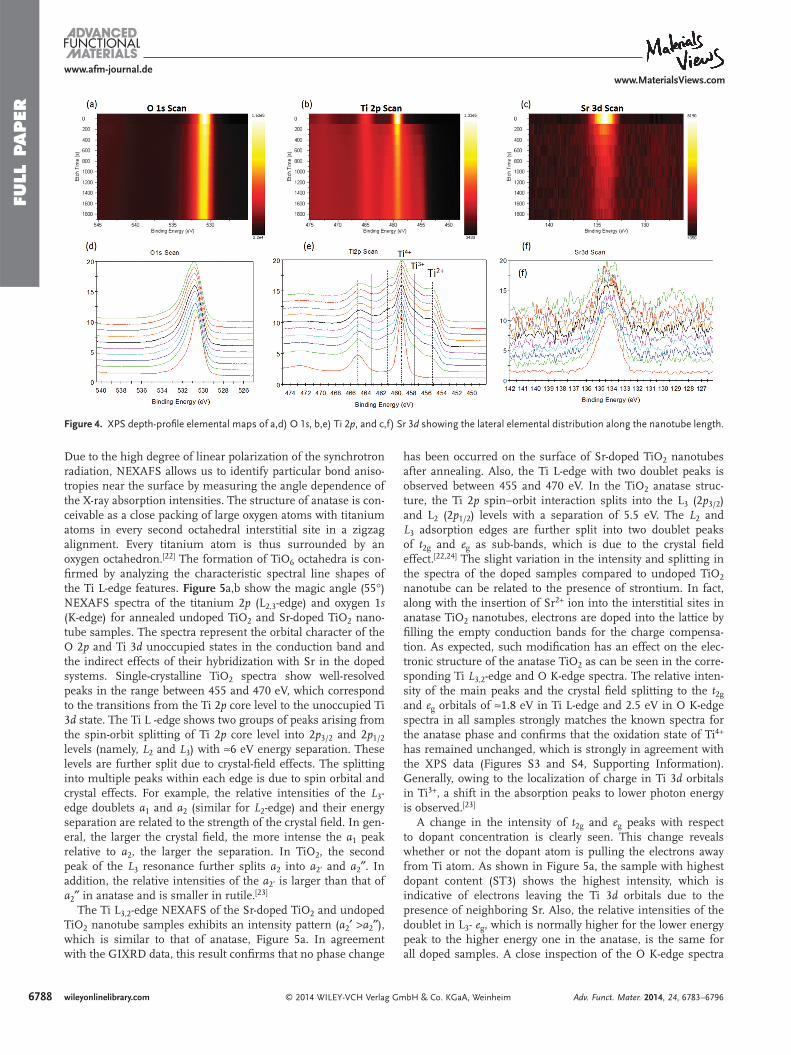
The XPS depth profi le analysis was performed to obtain infor-mation about the lateral elemental distribution along the length of the nanotubes in doped samples. Figure 4 shows a typical depth profi le of the Sr-doped TiO 2 nanotubes displayed in a 2D colored map, which was performed along the vertical axis of the nanotube. Note the observed shift from the fi rst scan to the subsequent scans indicating an actual difference between the charge conditions of the top layer, that is, the unsputtered layer of a sample and the subsurface sputtered layers. This shift is caused from a new charge equilibrium occurring as the sputter gun ions interact with the surface. Figure 4 a shows the O 1 s map with a homogeneous distribution of lattice oxygen along the nanotube. The stacked depth profi le plot of the O 1 s photoemission spectra is shown in Figure 4 d. A comparison between the O 1 s peak of the fi rst and the last scans revealed the presence of a peak broadening. A careful peak fi tting anal-ysis of this broadened peak revealed the Sr-O contribution at 532.3 eV in a small portion to the O 1 s peak in addition to two other peaks occurring at 531.4 eV and 530.4 eV, which can be attributed to the Ti-O contribution with O and Ti at different chemical states (from the nonstoichiometry induced in the TiO 2 structure by the presence of dopant). It should be noted that the attribution of the shoulder peak at higher binding energy (≈532 eV) to chemisorbed oxygen is not valid, because the etching process is performed in the vacuum chamber and there is low chance for the bombarded oxygen atoms making new bonds with the surface. Figure 4 b shows the Ti 2 p map with a fairly noticeable change in the distribution of Ti 2 p core level photoemissions, which reveals variation of the oxidation state of Ti from the surface along the nanotube. This can be well explained based on the stacked depth profi le Ti 2 p pho-toemission spectra shown in Figure 4 e. It can be seen from this spectra that as we move from the surface toward the bulk of the nanotubes, the doublet peaks of Ti 4+ start to shrink and shoulder peaks associated with Ti 3+ and Ti 2+ start to develop at 457.5 eV and 455 eV that correspond to the partial reduction of Ti 4+ to Ti 3+ and Ti 2+ states, respectively. It should be men-tioned that the depth profi ling XPS experiment has been car-ried out in a separate analysis chamber after annealing of the doped nanotubes; thus, the surfaces of the nanotubes were fur-ther oxidized upon exposure to air during the transport from the growth chamber to the analytical setup, which may result in re-oxidation of Ti 3+ and Ti 2+ back to Ti 4+ on the very top surface. The detailed XPS analysis as a function of dopant concentration for as-anodized and annealed Sr-doped TiO 2 nanotubes is pro-vided in Figure S3 and S4, Supporting Information.
To probe the local changes in the electronic structure and chemical bonding in doped TiO 2 nanotubes, the near edge X-ray absorption fi ne structure (NEXAFS) soft X-ray absorption spectra is used. The directional electric fi eld vector (E) of the X-rays can be used to probe the direction of chemical bonds of the atoms. NEXAFS, with sampling depth of a few nanom-eters, was performed in partial electron yield mode at the tita-nium L-edge (445−490 eV) and the oxygen K-edge (520−590 eV) regions. The data here are shown with a normalized edge step of 1 so that all spectra can be compared on a per atom basis.
Adv. Funct. Mater. 2014, 24, 6783–6796
www.afm-journal.dewww.MaterialsViews.com
Table 2. Kröger−Vink and traditional notation of defects for TiO 2 and Sr 2+ -doped TiO 2 .
Traditional notation Description Kröger−Vink notation
Ti Ti 4+ Ti Ti 4+ ion in the titanium
lattice site
Ti Ti x
Ti Ti 3+ Ti Ti 3+ ion in the titanium
lattice sitee′
V Ti Titanium vacancy V Ti ′′′′
Ti i 3+ Ti i 3+ in the interstitial site Ti i •••
Ti i 4+ Ti i 4+ in the interstitial site Ti i ••••
O O 2− O O 2- ion in the oxygen
lattice site
O O x
V O Oxygen vacancy V O ••
O O − O O − ion in the oxygen
lattice site
h •
Sr Ti 2+ Sr Ti 2+ ion in the titanium
lattice siteSr Ti ′′
Sr i 2+ Sr i 2+ ion in the interstitial
site
Sr i ••
Table 3. Basic defect equilibria in TiO 2 using Kröger−Vink notation .
xO V 2e / OO O1
2 2↔ + ′ + (1)
x xTi 2O Ti 3e OTi O i 2+ ↔ + ′ + (2)
x xTi 2O Ti 4e OTi O i 2+ ↔ + ′ + (3)
xO V 4h 2O2 Ti O↔ ′′′′ + + (4)
nil e h↔ ′ + (5)
FULL
PAPER
6788 wileyonlinelibrary.com © 2014 WILEY-VCH Verlag GmbH & Co. KGaA, Weinheim
Due to the high degree of linear polarization of the synchrotron radiation, NEXAFS allows us to identify particular bond aniso-tropies near the surface by measuring the angle dependence of the X-ray absorption intensities. The structure of anatase is con-ceivable as a close packing of large oxygen atoms with titanium atoms in every second octahedral interstitial site in a zigzag alignment. Every titanium atom is thus surrounded by an oxygen octahedron. [ 22 ] The formation of TiO 6 octahedra is con-fi rmed by analyzing the characteristic spectral line shapes of the Ti L-edge features. Figure 5 a,b show the magic angle (55°) NEXAFS spectra of the titanium 2 p (L 2,3 -edge) and oxygen 1 s (K-edge) for annealed undoped TiO 2 and Sr-doped TiO 2 nano-tube samples. The spectra represent the orbital character of the O 2 p and Ti 3 d unoccupied states in the conduction band and the indirect effects of their hybridization with Sr in the doped systems. Single-crystalline TiO 2 spectra show well-resolved peaks in the range between 455 and 470 eV, which correspond to the transitions from the Ti 2 p core level to the unoccupied Ti 3 d state. The Ti L -edge shows two groups of peaks arising from the spin-orbit splitting of Ti 2 p core level into 2 p 3/2 and 2 p 1/2 levels (namely, L 2 and L 3 ) with ≈6 eV energy separation. These levels are further split due to crystal-fi eld effects. The splitting into multiple peaks within each edge is due to spin orbital and crystal effects. For example, the relative intensities of the L 3 -edge doublets a 1 and a 2 (similar for L 2 -edge) and their energy separation are related to the strength of the crystal fi eld. In gen-eral, the larger the crystal fi eld, the more intense the a 1 peak relative to a 2 , the larger the separation. In TiO 2 , the second peak of the L 3 resonance further splits a 2 into a 2’ and a 2″ . In addition, the relative intensities of the a 2’ is larger than that of a 2″ in anatase and is smaller in rutile. [ 23 ]
The Ti L 3,2 -edge NEXAFS of the Sr-doped TiO 2 and undoped TiO 2 nanotube samples exhibits an intensity pattern ( a 2′ > a 2″ ), which is similar to that of anatase, Figure 5 a. In agreement with the GIXRD data, this result confi rms that no phase change
has been occurred on the surface of Sr-doped TiO 2 nanotubes after annealing. Also, the Ti L-edge with two doublet peaks is observed between 455 and 470 eV. In the TiO 2 anatase struc-ture, the Ti 2 p spin−orbit interaction splits into the L 3 (2 p 3/2 ) and L 2 (2 p 1/2 ) levels with a separation of 5.5 eV. The L 2 and L 3 adsorption edges are further split into two doublet peaks of t 2g and e g as sub-bands, which is due to the crystal fi eld effect. [ 22,24 ] The slight variation in the intensity and splitting in the spectra of the doped samples compared to undoped TiO 2 nanotube can be related to the presence of strontium. In fact, along with the insertion of Sr 2+ ion into the interstitial sites in anatase TiO 2 nanotubes, electrons are doped into the lattice by fi lling the empty conduction bands for the charge compensa-tion. As expected, such modifi cation has an effect on the elec-tronic structure of the anatase TiO 2 as can be seen in the corre-sponding Ti L 3,2 -edge and O K-edge spectra. The relative inten-sity of the main peaks and the crystal fi eld splitting to the t 2g and e g orbitals of ≈1.8 eV in Ti L-edge and 2.5 eV in O K-edge spectra in all samples strongly matches the known spectra for the anatase phase and confi rms that the oxidation state of Ti 4+ has remained unchanged, which is strongly in agreement with the XPS data (Figures S3 and S4, Supporting Information). Generally, owing to the localization of charge in Ti 3 d orbitals in Ti 3+ , a shift in the absorption peaks to lower photon energy is observed. [ 23 ]
A change in the intensity of t 2g and e g peaks with respect to dopant concentration is clearly seen. This change reveals whether or not the dopant atom is pulling the electrons away from Ti atom. As shown in Figure 5 a, the sample with highest dopant content (ST3) shows the highest intensity, which is indicative of electrons leaving the Ti 3 d orbitals due to the presence of neighboring Sr. Also, the relative intensities of the doublet in L 3 - e g , which is normally higher for the lower energy peak to the higher energy one in the anatase, is the same for all doped samples. A close inspection of the O K-edge spectra
Adv. Funct. Mater. 2014, 24, 6783–6796
www.afm-journal.dewww.MaterialsViews.com
Figure 4. XPS depth-profi le elemental maps of a,d) O 1 s , b,e) Ti 2 p , and c,f) Sr 3 d showing the lateral elemental distribution along the nanotube length.

FULL P
APER
6789wileyonlinelibrary.com© 2014 WILEY-VCH Verlag GmbH & Co. KGaA, Weinheim
(Figure 5 b) reveals slight changes in the intensity as well as the t 2g - e g splitting with respect to doping content. The decrease in intensities of the doped samples is an evidence of a reduction in O 2 p –Ti 3 d bands, which is consistent with the higher inten-sity of the corresponding Ti L-edge NEXAFS in doped samples compared to the undoped TiO 2 . In fact, this further implies charge relocation from Ti 3 d to O 2 p, which results in Ti–O bonds becoming more ionic. On the other hand, the magnitude of this splitting depends on the strength of the fi eld created by the point charges, which is in turn affected by the point charge distance from the central atom and from the overall magni-tude of each charge. The observed decrease in the magnitude of splitting relative to the amount of dopant indicates that the presence of Sr may cause the O atoms to occupy sites at dif-ferent distances from the Ti atoms. Therefore, this will create different degrees of distortion and/or different stacking of the octrahedra. As the distance between the Sr and O atoms is less, in this case, than the Sr to Ti atoms, the O orbitals are more likely to be affected by adjacent dopant atom. Therefore, it can be concluded that Sr 2+ doping only alters the Ti and O ions
interaction in the TiO 2 lattice on the surface and has no evident effect on their individual charge states.
The NEXAFS data were also measured at different incident beam angles on the ST3 sample (Figure 5 c,d). In order to probe the Ti-O bond directionality, the data were collected by varying the angle between the electric fi eld vector of the X-rays and the surface of the nanotube arrays with the photon beam fi xed at parallel, in 55° and perpendicular to the surface normal of the sample. The inset in Figure 5 d illustrates the relation between the X-ray incident beam and the X-ray electric fi eld vector (E) with respect to the nanotubes orientation in the sample used for NEXAFS experiment. At the magic angle of 55°, where the orientation effect is minimal, the intensity of the peak is decreased because the effect from different crystals with dif-ferent orientations is canceled out. At grazing incidence, where the incident beam is nearly parallel to the surface of the nano-tubes (which means also normal to the nanotube walls), the E has the larger projection along the tube axis. Therefore, the crystal orientation along the tube wall is mostly inspected in this case. The lowest intensity observed at this incident angle
Adv. Funct. Mater. 2014, 24, 6783–6796
www.afm-journal.dewww.MaterialsViews.com
Figure 5. NEXAFS spectra of a) titanium 2 p (L 2,3 -edge) and b) oxygen 1 s (K-edge) for annealed (crystalline) TiO 2 and Sr 2+ -doped TiO 2 nanotube samples with three different dopant concentrations taken at magic angle. NEXAFS spectra of c) titanium 2 p (L 2,3 -edge) and d) oxygen 1 s (K-edge) recorded on the Sr-doped TiO 2 nanotubes (sample ST3) in three experimental geometries: E parallel, in 55° and perpendicular to the principal axis of the nano-structure. Schematic of the relation between X-ray incident beam and the X-ray electric fi eld vector (E) with respect to the nanotubes orientation used for the NEXAFS experiments is shown in the inset of (b).

FULL
PAPER
6790 wileyonlinelibrary.com © 2014 WILEY-VCH Verlag GmbH & Co. KGaA, Weinheim
reveals that only part of the orbitals contribute to the intensity, which is consistent with the preferred orientation of the octahe-dral planes in the x-y plane.
Figure 5 c,d illustrate the NEXAFS spectra of titanium 2 p (L 2,3 -edge) and oxygen 1 s (K-edge) in three different experi-mental geometries shown in the schematic. The Ti L-edge spectra (Figure 5 c) are similar to those reported earlier for the TiO 2 anatase phase in terms of the shape of the peaks and the crystal fi eld splitting, but with the main discrepancy in the intensities with respect to the E direction. Starting by the normal incidence, which has the highest intensity in the Ti L-edge spectra, the E vector that is normal to the incident beam has also the largest projection in the direction normal to the tube wall. Therefore, the higher intensity of the peaks in this direction implies the existence of a preferential orientation of the crystals in a specifi c direction where E vector is highly involved in the promotion of the electrons from occupied to unoccupied orbitals. The O K-edge spectra are also similar to those reported earlier for the TiO 2 anatase phase in terms of the shape of the peaks and the crystal fi eld splitting (Figure 5 d). However, we do not observe as much of variation in terms of orientation dependency for the oxygen by varying the incident beam direction from grazing angle toward the normal direction in these spectra. This could be attributed to the fact that most of the information in the O K-edge spectrum is coming from the amorphous portion in the outer layer and on the surface rather than the oxygen in TiO 2 lattice structure.
The texture analysis of the nanotube arrays is performed to understand the relation between crystal orientation distribution
in polycrystalline undoped and Sr-doped TiO 2 NTAs in the bulk. The distribution of crystal planes in both samples are shown in the XRD pole-patterns in Figure 6 . Comparison of the XRD pole patterns in undoped and doped samples with the highest dopant content revealed a drastic change in preferential orientation distribution of the (004) planes (as shown with the highest intensity) after doping. As can be seen, the (004) planes in undoped TiO 2 NTAs are relatively parallel to the vertical axis of the nanotubes; however, when the sample is doped, the ori-entation distribution of these planes change. Such variations in the crystal orientation distribution in the bulk can be similarly attributed and linked to the variations in the alignment of octa-hedral units due to the presence of dopant atom in the crystal lattice averaged over the surface. [ 25 ]
2.4. Doping Mechanism at the Atomic Scale
A clearer insight toward the understanding of the doping mechanism at the atomic scale is obtained from HRTEM and Z-contrast ADF-STEM imaging combined with EELS spectra acquisition of the surface of a single Sr-doped TiO 2 nanotube (sample ST3) in STEM mode. Figure 7 a shows the Z-contrast ADF-STEM image of a single nanotube probed from the top surface. This image is deliberately taken on a coarser length scale to observe the presence of any distributed clusters. The Sr-M 4,5 , Ti-L 2,3 and O-K edges are used to extract the EELS SI mapping data with the details of background subtraction in Sr M-edge spectra provided in Figures S5–S8, Supporting
Adv. Funct. Mater. 2014, 24, 6783–6796
www.afm-journal.dewww.MaterialsViews.com
Figure 6. XRD pole-patterns of (101), (004), and (200) planes measured at fi xed 2 θ angles of 25.38°, 38.5°, and 48° on undoped TiO 2 NTAs (top) and Sr-doped TiO 2 NTAs (ST3 sample) (bottom).

FULL P
APER
6791wileyonlinelibrary.com© 2014 WILEY-VCH Verlag GmbH & Co. KGaA, Weinheim
Information. A signifi cant contrast change in Z -contrast images was observed between some regions on the surface of the ring, with the brighter regions indicating the presence of heavier elements than Ti in the anatase structure. The method of Botton [ 26 ] has been used here to extract the Sr M-edge map, which matches well with the Sr position edge and has become more pronounced after removing plural scattering. The Sr M map also matches well with the bright contrast in the SI survey image. From the EELS-SI map of oxygen, titanium and stron-tium, it appears that the O and Ti are uniformly distributed on the surface whereas the Sr is mostly segregated at the inner edge of the tube. This is clearly observable from the Z-contrast image taken at higher magnifi cation on the ring as shown in Figure 7 e. As can be seen from the STEM SI maps, the bulk region of the ring is composed of a homogeneous distribution of Ti and O; however, a nanometer size cluster of Sr-rich region is formed at the most interior boundary of the nanotube sur-rounded by Ti and O containing medium.
Comparison of Ti-L 2,3 signals from different regions on the surface of the doped nanotube is shown in Figure 8 . Note that the signal intensity of Ti-L 2,3 varies between the scans over Ti-rich regions in the middle and the Sr-rich regions at the edges on the ring. A signifi cant change is observed for scans over the magnifi ed Sr-rich region as shown in Figure 8 c,f. In certain cases, the segregation-induced enrichment of the surface layer results in the formation of low-dimensional surface structures. This is the case when the local concentrations surpass certain critical limits. [ 20 ] This result reveals that in the highest doped nanotube sample, as we move toward the interior edge of the nanotube, the Sr-rich region segregates into nanoclusters of a completely new phase forming hetero-nanostructures (HNSs) that gradually merges into the TiO 2 lattice in intimate vicinity of the interface.
Figure 9 shows the Z -contrast STEM images of a few rings of Sr-doped TiO 2 nanotubes. It is noticed that the Z -contrast intensity is drastically changing between the two heterophases, Figure 9 a. The atomic structure of the segregated nanoclusters
was seen to be matching the cubic lattice of SrO with the meas-ured lattice parameter of 0.26 nm.
Figure 10 a shows the atomic resolution Z -contrast STEM images of different regions (shown with letters: a, b and c in Figure 10 a) on the surface of a nanotube ring. The middle region of the ring (specifi ed as region b) is shown in Figure 10 b which reveals the arrangement of the Ti atoms in the anatase TiO 2 with tetragonal structure and the lattice parameters as measured in FFT reconstructed image of a = b = 0.38 nm. A few bright spots can also be observed in this image. As we go along the arrow to region c, a number of bright spots start to appear in the vicinity of the TiO 2 lattice. These bright spots cor-respond to Sr atoms that are randomly distributed in the lat-tice of TiO 2 and have caused displacement of some atoms from their original position in the lattice. The nanoclusters were also observed to be changing gradually to a similar structure to that of TiO 2 matrix at the vicinity of the hetero-interface. However, as we get close to the interior edge of the ring, the segregated SrO clusters with cubic structure are observed with the atomic arrangement in (111) planes as shown in FFT reconstructed image. The d -spacing from these regions are measured to be in the range from 0.293 to 0.298 nm, corresponding to the (111) planes. As a result, it can be concluded that such preferential growth of the SrO on the surface and at the interior edges of the nanotubes can be related to the disordering and instability of the surface atoms acting as nucleation sites for the growth of nanoclusters. The signifi cance of the formation of SrO nano-clusters in the TiO 2 anatase matrix, due to the effect of the pres-ence of the hetero-interface between the SrO and TiO 2 , lies in the fact that it can drastically affect the photocatalytic effi ciency of the material as reported by Chen et al. [ 27 ] They showed SrO-coated TiO 2 nanotubes to have higher solar-to-electricity conver-sion effi ciency ( η ) than the uncoated nanotubes. This improve-ment has been related to the possible effect from the presence of the SrO as a thin potential barrier layer that inhibits the charge recombination at the electrode/electrolyte interface, thereby increasing the effi ciency. It has been also suggested
Adv. Funct. Mater. 2014, 24, 6783–6796
www.afm-journal.dewww.MaterialsViews.com
Figure 7. a) Z -contrast STEM image of the surface of a single Sr-doped TiO 2 nanotube (taken from sample ST3), b–d) the corresponding EELS-SI map of oxygen, titanium and strontium, respectively. e) Higher magnifi cation Z -contrast STEM image of the surface of a single Sr-doped TiO 2 nanotube and f–g) the corresponding EELS-SI map of oxygen, titanium and strontium, respectively.

FULL
PAPER
6792 wileyonlinelibrary.com © 2014 WILEY-VCH Verlag GmbH & Co. KGaA, Weinheim Adv. Funct. Mater. 2014, 24, 6783–6796
www.afm-journal.dewww.MaterialsViews.com
that there is a possibility that the treatment with SrO can form a surface layer of SrTiO 3 on TiO 2 nanotubes, (with higher CB level than pure TiO 2 ), an effect that has been previously shown to improve the photoelectrochemical effi ciency of the entire material system. [ 11,28 ]
2.5. Photoelectrochemical Activity
To demonstrate a proof-of-concept photoelectrochemical activity of the Sr-doped TiO 2 nanotube arrays for water photoelectrol-ysis, the incident photon conversion effi ciency (IPCE) experi-ments were performed in a two-electrode arrangement with the nanotube fi lm as the working photoelectrode and platinum foil as a counter electrode in 1.0 M KOH solution. Figure 11 shows the obtained IPCE for undoped and Sr-doped (ST3) TiO 2 nano-tube samples as a function of the irradiation wavelength under
a DC bias of 0.6V. The IPCE was calculated using Equation ( 3) , where λ is the wavelength of incident light, i ph is the photocur-rent density under illumination at λ , and I o is the incident light intensity at λ .
i
IIPCE%=
(1240eVnm)( mAcm )
( nm)( mWcm )100
ph2
o2λ
×−
−
(3)
The undoped TiO 2 nanotubes showed an IPCE as high as 50% in the wavelength range 200–400 nm, indicating the high quality of the fabricated fi lm. Doping TiO 2 with Sr (ST3) resulted in an enhancement in the IPCE up to 65%, with a slight red-shift in the wavelength which is in accordance with the absorption spectra for the same material reported in our previous study. [ 12 ] Note that the IPCE declines after 400 nm, indicating that the photocurrent occurs as a result of the band gap transition. The IPCE values at 500–600 nm (visible region)
Figure 8. a–c) Top view Z-contrast STEM images of the surface of a single Sr-doped TiO2 nanotube (taken from sample ST3) at different magnifi cations; d–f) the corresponding Ti L-edge EELS spectra taken from two spots in the selected region on the STEM image on the ring.

FULL P
APER
6793wileyonlinelibrary.com© 2014 WILEY-VCH Verlag GmbH & Co. KGaA, WeinheimAdv. Funct. Mater. 2014, 24, 6783–6796
www.afm-journal.dewww.MaterialsViews.com
of TiO 2 nanotube arrays is due to the interference from the tita-nium substrate. [ 29 ] Similarly, an interference pattern is typically observed in the absorption spectrum as a result of light absorp-tion in the titanium substrate. [ 30 ] The enhancement in photoac-tivity of the titania nanotubes upon their doping with Sr, makes this material architecture a great potential for water splitting applications.
3. Conclusions
The fabrication of Sr-doped TiO 2 nanotubes via one step elec-trochemical anodization technique was demonstrated. The effect of dopant concentration on the nanotubes surface and bulk properties, the uniformity of doping along the nanotubes length and radial direction as well as the doping mechanism was discussed by detailed analysis of the bulk structure and surface characteristics of the doped nanotubes using GIXRD, XPS and NEXAFS measurements. At low dopant concentra-tions, Sr-doping results in the expansion of the tetragonal lat-tice of the TiO 2 nanotubes. Furthermore, the insertion of the dopant was found to change the oxidation state of Ti along the length of the nanotubes. The NEXAFS surface analysis of the doped nanotubes revealed that Sr 2+ doping only alters the Ti and O ions interaction in the TiO 2 lattice on the surface and has no evident effect on their individual charge states. In addi-tion, NEXAFS experiments performed at different incident beam angles revealed a relation between the preferential crystal
orientation in the bulk of the nanotubes and the orientation of the octahedral units on their surface. The combination of high-resolution Z-contrast imaging and EELS SI mapping also revealed a possible phase segregation of SrO on the surface of the nanotubes at high doping content. Formation of such het-erointerfaces between the SrO and TiO 2 phases can be consid-ered as a key feature in the investigation of the photocatalytic properties of the material. The results of the surface and bulk analyses suggested that the structural modifi cation from Sr dopant in the TiO 2 nanotube lattice was strongly sensitive to the dopant concentration as well as the growth conditions. The interpretation from the induced surface and bulk structural changes in the TiO 2 nanotubes due to aliovalent doping and its correlation with the observed enhancement in the visible light activity of the doped titania nanotube arrays in this study may be applicable into characterization and better understanding the photoelectrochemical properties of other types of in situ doped solution-derived metal-oxide nanomaterial assemblies.
4. Experimental Section Synthesis of Undoped and Strontium-Doped TiO 2 NTAs : Arrays of
closed-end highly ordered vertically oriented pristine TiO 2 and Sr-doped TiO 2 nanotube arrays (with an average inner diameter of ∼100 nm) were grown using potentiostatic anodization technique on 2 cm × 2 cm strips of polished titanium (0.25 mm thick, Alfa Aesar) in a two-electrode electrochemical cell. Prior to anodization, the strips were rinsed in an ultrasonic bath of ethanol and DI water for 1 h and 15 min, respectively.
Figure 9. a) Z -contrast STEM image of the surface of a few rings of Sr-doped TiO 2 nanotubes (taken from sample ST3). b,c) High resolution images taken from specifi ed regions in (a) showing segregation of cubic SrO at the edge with the lattice parameter of 0.26 nm in the simulated image in inset.

FULL
PAPER
6794 wileyonlinelibrary.com © 2014 WILEY-VCH Verlag GmbH & Co. KGaA, Weinheim Adv. Funct. Mater. 2014, 24, 6783–6796
www.afm-journal.dewww.MaterialsViews.com
Pt mesh was used as the counter electrode and located 2 cm away from the Ti electrode immersed in the electrolyte. Samples were anodized and doped in situ in aqueous electrolytes containing NH 4 F (0.1 M ) mixed with anhydrous strontium hydroxide (0.02 M , 0.04 M , and 0.06 M Sr (OH) 2 , 99% from Pfaltz and Bauer Inc.) at 20 V for 3 h at 20 °C. The pH of the electrolyte was controlled and kept constant at 3 by the addition of H 3 PO 4 to the solution. After anodization, the samples were ultrasonically rinsed in DI water and dried under a stream of nitrogen. Subsequently, samples were annealed at 450 °C for 4 h with heating and cooling rates of 1 °C min −1 . The undoped TiO 2 NTAs and the lowest to the highest strontium- containing doped samples are named hereafter T, ST1, ST2 and ST3, respectively. The dopant concentrations were measured by inductively coupled plasma mass spectrometry (ICP MS) in standard mode using a PerkinElmer ELAN 9000 instrument.
Bulk Characterization of Undoped and Strontium-Doped TiO 2 NTAs : The morphology of the nanotubes was examined using a fi eld emission scanning electron microscope (FESEM-Zeiss SEM Ultra60). The analysis of the atomic structure and the chemical composition of the nanotubes were carried out using a 200 KV atomic resolution transmission electron microscope (JEOL, JEM-ARM200F). For TEM observations, TiO 2 nanotube fi lms were scratched off from the (titanium or silicon) substrate and were dissolved in ethanol followed by grinding. The dried powder-like samples were supported on Cu mesh with a carbon micro-grid. The TEM, high resolution TEM (HRTEM) and the high angle annular dark-fi eld scanning transmission electron microscopy (HAADF-STEM) observations were performed using an aberration-corrected
cold fi eld emission scanning transmission electron microscope. The electron energy loss spectroscopy (EELS) and EELS spectrum imaging (EELS-SI) measurements were also performed using a Gatan GIF Quantum spectrometer. Additionally, the doped nanotubes were imaged using aberration-corrected atomic number contrast STEM (Z-STEM). All the TEM image processing has been performed using Gatan’s Digital Micrograph software. Glancing incidence X-ray diffractometer (GIXRD; PANalytical X’Pert PRO diffractometer with Cu Kα radiation) was used for the structural measurements.
Surface Characterization of Undoped and Strontium-Doped TiO 2 NTAs : The surface composition of the samples was analyzed by X-ray photoelectron spectroscopy using a Thermo Scientifi c K-alpha XPS with an Al anode. Spectra were charge referenced to O 1 s at 532 eV. Based on the relative sputtering rates reported for the Ta 2 O 5 and TiO 2 , using the same ion energy in Baer et al., [ 31 ] the sputter rate of TiO 2 was estimated to be ≈0.14 nm s −1 . The depth profi ling was carried out on a spot size of 400 μm and every scan was performed after each etching cycle of 3 min on the sample. A total of 9 cycles were performed resulting in etching of about 324 nm of the material (≈1.3 of the tube length) along the nanotubes. The O 1 s , Ti 2 p and Sr 3 d scans were recorded on the sample after each cycle. Based on the etching rate, the depth of each cycle was estimated to about 25 nm. The etching rate of the instrument was calibrated using a Ta 2 O 5 standard (0.19 nm s −1 for the Ar+ ion energy of 2000 eV). Synchrotron near-edge X-ray absorption fi ne structure (NEXAFS) was used to investigate the electronic structure of the samples. The NEXAFS was performed by acquiring peak intensities
Figure 10. a–d) Atomic resolution Z -contrast STEM images of the surface of a ring of Sr-doped TiO 2 nanotube (taken from sample ST3) showing the distribution of Sr in different regions on the surface.

FULL P
APER
6795wileyonlinelibrary.com© 2014 WILEY-VCH Verlag GmbH & Co. KGaA, WeinheimAdv. Funct. Mater. 2014, 24, 6783–6796
www.afm-journal.dewww.MaterialsViews.com
as a function of the incident X-ray photon energy in the vicinity of the titanium L-edge (445−490 eV) and the oxygen K-edge (520−590 eV) regions. The data were taken using a partial electron yield (PEY) detector and a 270 V rejection bias at the NIST beam line U7A located at the National Synchrotron Light Source in Brookhaven National Laboratory. Simultaneous reference signals were collected from a TiN mesh and used to energy-calibrate the partial electron yield (PEY) signals. A 1200 l mm −1 grating was used together with 30 um × 30 um slits to energy select the incident beam. A 0.1 eV/step energy resolution was used within at least ± 20 eV of the absorption edge. In order to probe the Ti-O bond directionality, the incident angle of the X-ray beam, which exhibits high linear polarization of the electric fi eld vector, was varied and NEXAFS data was collected with the beam set at 20°, at 55° and perpendicular to the surface plane of the sample. Spectra taken at 20o will be referred to as “parallel” in the remainder of the manuscript. The fi nal spectra were generated by post-processing this intensity versus energy dataset within various regions of the sample using the Athena program.
Photoelectrochemical Measurements : The incident photon conversion effi ciency (IPCE) experiments were performed in a two-electrode arrangement with the nanotube fi lm as the working photoelectrode and platinum foil as a counter electrode in 1.0 M KOH solution under a DC bias of 0.6 V.
Supporting Information Supporting Information is available from the Wiley Online Library or from the author.
Acknowledgements This work was funded by Pacifi c Northwest National Laboratory (PNNL). The TEM work was carried out at Florida State University, and the TEM facility at FSU is funded and supported by the Florida State University Research Foundation, National High Magnetic Field Laboratory (NSF-DMR-0654118) and the State of Florida. We acknowledge the support of the American Chemical Society Petroleum Research Fund
(# 50934-DNI10) and the U. S. National Science Foundation (grant number OISE-1103827). Use of the National Synchrotron Light Source, Brookhaven National Laboratory, was supported by the U.S. Department of Energy, Offi ce of Science, Offi ce of Basic Energy Sciences, under Contract No. DE-AC02-98CH10886.
Received: May 30, 2014 Revised: June 28, 2014
Published online: August 28, 2014
[1] S. G. Kumar , L. G. Devi , J. Phys. Chem. A 2011 , 115 , 13211 .
[2] N. K. Allam , Ph.D. Thesis , The Pennsylvania State University , PA, USA 2009 .
[3] L. Chiodo , J. M. Garcia-Lastra , D. J. Mowbray , A. Iacomino , A. Rubio , arXiv:1003.2341, 2010 .
[4] J. M. Macak , H. Tsuchiya , A. Ghicov , K. Yasuda , R. Hahn , S. Bauer , P. Schmuki , Curr. Opin. Solid State Mater. Sci. 2007 , 11 .
[5] I. M. Low , H. Albetran , V. M. Prida , V. Vega , P. Manurung , M. Ionescu , J. Mater. Res. 2013 , 28 , 304 .
[6] L. Wen , B. Liu , X. Zhao , K. Nakata , T. Murakami , A. Fujishima , Int. J. Photoenergy 2012 , 2012 , 1 .
[7] Y.-C. Nah , I. Paramasivam , P. Schmuki , Chem. Phys. Chem. 2010 , 11 , 2698 .
[8] A. Kumar , P. G. Santangelo , N. S. Lewis , J. Phys. Chem. 1992 , 96 , 834 .
[9] Y. Liu , L. Xie , Y. Li , R. Yang , J. Qu , Y. Li , X. Li , J. Power Sources 2008 , 183 , 701 .
[10] M. Ueda , S. Otsuka-Yao-Matsuo , Sci. Tech. Adv. Mater. 2003 , 5 , 187 .
[11] J. Zhang , J. H. Bang , C. Tang , P. V. Kamat , ACS Nano 2010 , 4 , 387 .
[12] H. A. Hamedani , N. K. Allam , H. Garmestani , M. A. El-Sayed , J. Phys. Chem. C 2011 , 115 , 13480 .
[13] E. Ernst , M.S. Thesis, Georgia Institute of Technology , GA, USA 2007 .
[14] M. F. d. Campos , J. C. Damasceno , R. Machado , C. A. Achete , presented at the XVIII IMEKO WORLD CONGRESS, Metrology for a Sustainable Development, Rio de Janeiro, Brazil, September 2006 .
[15] M. Steveson , T. Bredow , A. R. Gerson , Phys. Chem. Chem. Phys. 2002 , 4 , 358 .
[16] R. D. Shannon , C. T. Prewitt , Acta Crystallog. 1969 , B25 , 925 . [17] R. Gallay , J. J. van der Klink , J. Moser , Phys. Rev. B 1986 , 34 ,
3060 . [18] U. Gesenhues , T. Rentschler , J. Solid State Chem. 1999 , 143 , 210 . [19] F. Kröger , H. Vink , Solid state phys. 1956 , 3 , 307 . [20] A. J. Atanacio , T. Bak , J. Nowotny , ACS Appl. Mater. Interfaces 2012 ,
4 , 6626 . [21] T.-j. Chen , P. Shen , J. Phys. Chem. C 113 , 2009 , 328 . [22] C. Bittencourt , A. Felten , X. Gillon , J. J. Pireaux , E. Najafi ,
A. P. Hitchcock , X. Ke , G. Tendeloo , C. P. Ewels , P. Umek , D. Arcon , Proc. of The 14th European Microscopy Congress (Eds: M. Luysberg , K. Tillmann , T. Weirich ), Springer Berlin Heidelberg, Germany 2008 .
[23] J. G. Zhou , H. T. Fang , J. M. Maley , M. W. Murphy , J. Y. P. Ko , J. N. Cutler , R. Sammynaiken , T. K. Sham , M. Liu , F. Li , J. Mater. Chem. 2009 , 19 , 6804 .
[24] P. Guttmann , C. Bittencourt , X. Ke , G. V. Tendeloo , P. Umek , D. Arcon , C. P. Ewels , S. Rehbein , S. Heim , G. Schneider , Proc. of The 10th International Conference on X-Ray Microscopy (Eds: A. Waldron ), AIP Publishing , New York 2011 .
[25] A. Lotnyk , S. Senz , D. Hesse , J. Phys. Chem. C 2007 , 111 , 6372 .
[26] G. A. Botton , S. Lazar , C. Dwyer , Ultramicroscopy 2010 , 110 .
Figure 11. The IPCE plots for undoped and Sr-doped titanium dioxide nanotube array fi lms under an applied dc potential of 0.6 V.

FULL
PAPER
6796 wileyonlinelibrary.com © 2014 WILEY-VCH Verlag GmbH & Co. KGaA, Weinheim Adv. Funct. Mater. 2014, 24, 6783–6796
www.afm-journal.dewww.MaterialsViews.com
[27] J.-G. Chen , C.-Y. Chen , C.-G. Wu , C.-Y. Lin , Y.-H. Lai , C.-C. Wang , H.-W. Chen , R. Vittal , K.-C. Ho , J. Mater. Chem. 2010 , 20 , 7201 .
[28] J. Zhang , C. Tang , J. H. Bang , Electrochem. Commun. 2010 , 12 , 1124 . [29] P. Chen , J. Brillet , H. Bala , P. Wang , S. M. Zakeeruddin , M. Gratzel ,
J. Mater. Chem. 2009 , 19 , 5325 .
[30] Z. Liu , X. Zhang , S. Nishimoto , M. Jin , D. A. Tryk , T. Murakami , A. Fujishima , J. Phys. Chem. C 2007 , 112 , 253 .
[31] D. R. Baer , M. H. Engelhard , A. S. Lea , P. Nachimuthu , T. C. Droubay , B. L. J. Kim , C. Mathews , R. L. Opila , L. V. Saraf , W. F. Stickle , R. M. Wallace , B. S. Wright , J. Vac. Sci. Technol. A 2010 , 28 , 1060 .
Copyright © 2022 FDOKUMEN