
Design and development of a controller for a brushless doubly ...
81
AN ABSTRACT OF THE THESIS OF Virendra S. Javadekar for the degree of Master of Science in Electrical and Computer Engineering presented on January 31, 1992. Title : Design and Development of a Controller for a Brush less Doubly- Fed Automotive Alternator System ,Redacted for Privacy Abstract approved : Rene Spee The loads on the electrical systems of automobiles are projected to increase significantly in the near future. This will result in a requirement for improved efficiency over the present-day car alternators. An alternative scheme proposed at Oregon State University employs a Brushless Doubly-Fed Machine (BDFM) as an alternator. This thesis begins with a study and characterization of the existing car alternator system. The configuration of the proposed scheme is discussed. In the proposed configuration, the power winding of the machine generates the bulk of the power and the control winding provides the excitation. The power winding feeds a power rectifier, which in turn charges the battery in an automobile. The control winding is supplied through an inverter. Issues related to inverter and rectifier design are discussed. A 3-phase pulse width
-
Upload
khangminh22 -
Category
Documents
-
view
3 -
download
0
Transcript of Design and development of a controller for a brushless doubly ...

AN ABSTRACT OF THE THESIS OF
Virendra S. Javadekar for the degree of Master of Science in Electrical
and Computer Engineering presented on January 31, 1992.
Title : Design and Development of a Controller for a Brush less Doubly-
Fed Automotive Alternator System ,Redacted for Privacy
Abstract approved :Rene Spee
The loads on the electrical systems of automobiles are projected
to increase significantly in the near future. This will result in arequirement for improved efficiency over the present-day caralternators. An alternative scheme proposed at Oregon StateUniversity employs a Brushless Doubly-Fed Machine (BDFM) as an
alternator.
This thesis begins with a study and characterization of the
existing car alternator system. The configuration of the proposed
scheme is discussed. In the proposed configuration, the power
winding of the machine generates the bulk of the power and the
control winding provides the excitation. The power winding feeds a
power rectifier, which in turn charges the battery in an automobile.
The control winding is supplied through an inverter. Issues related to
inverter and rectifier design are discussed. A 3-phase pulse width

modulated inverter and a bridge rectifier were developed and tested
for performance. A PSPICE simulation model for the rectifier was
developed and results are compared with laboratory tests. A Voltage
Regulator Circuit (VRC) and an Efficiency Maximizer Unit (EMU) for
the system are designed and developed. A prototype alternator system
is tested and the principle of efficiency maximization is verified.
Finally, the comparative performance of the the existing and theproposed system is discussed and some recommendations for further
improvements in the prototype system are made.

Design and Development of a Controllerfor a
Brushless Doubly-Fed Automotive Alternator System
by
Virendra S. Javadekar
A THESIS
submitted to
Oregon State University
in partial fulfillment ofthe requirements for the
degree of
Master of Science
Completed January 31, 1992
Commencement June 1992

APPROVED:Redacted for Privacy
Assistant Professor of Electrical and Computer Engineeringin charge of major
Redacted for Privacy
Head of ent of Electrical and Computer Engineering
Redacted for Privacy
Dean of Graduaryhool d
Date thesis is presented January 31. 1992
Typed by Virendra S. Javadekar

ACKNOWLEDGEMENTS
As I put together the outcome of the work of the past two yearsin this thesis, I realize that it would have been impossible for me tohandle this task alone. I would like to take this opportunity to thankeach and everyone who has helped me during this course.
First of all, I would like to express my sincere thanks to Dr.Rene Spec, who has been someone more than a Major Professor to me.I am grateful to him for his valuable guidance to me during my entiregraduate program and thesis work. His trust in my abilities andenthusiasm for this project motivated me to work diligently.
I would also like to thank Dr. Alan K. Wallace and Dr. G. C.Alexander for their assistance to my thesis work and Dr. J. H. Herzogfor helping me in completing the requirements of my graduateprogram. I am thankful to Prof. Amort who allowed me to use theequipment from the Instrumentation laboratory at various timesduring my thesis work. My thanks to Prof. Keith Levien for attendingmy defense in the capacity of a GCR.
The work described in this thesis was supported by aconsortium consisting of The Bonneville Power Administration, PugetSound Power and Light, and The Electric Power Research Institute. Iam appreciative of the funding which made this work possible.
I acknowledge the assistance of my colleagues, D. K. Ravi, AshokRamchandran and Shibashis Bhowmik in conducting the laboratorytests.
At this moment, I cannot forget the strong moral support I havereceived from my family members in India for the last two years. I alsothank Mr. Dhoot, Mr. Joshi and Mr. Vaidya for backing my decision ofpursuing the M. S. degree.
Finally, I would like to dedicate this thesis to my Parents whoselove and faith in me have always been my source of inspiration.

TABLE OF CONTENTS
Chapter 1.
Introduction 1
Chapter 2.
Design of a 3-Phase Pulse Width Modulated (PWM)Inverter 9
2.1 Selection of Inverter Topology 9
2.2 Automotive PWM Inverter Design
Considerations 1 1
2.3 Power Circuit Design
Selection of Devices and Topology 12
2.4 Inverter Control Circuit 162.5 Inverter Performance 2 3
Chapter 3.
Design of 3-Phase Power Rectifier 283.1 Device Selection and Design 283.2 PSPICE Simulation and Laboratory
Performance Tests 2 9
Chapter 4
Design of Voltage Regulator and Efficiency Maximizer 3 5
4.1 Design of the Voltage Regulator 3 5
4.2 Performance Tests on VRC 38
4.3 Efficiency Maximizer Unit (EMU) 4 0
Chapter 5.
Test Results for the Brush less Doubly-Fed Automotive
Alternator (BDFAA) 48
Chapter 6.
Conclusions and Recommendations for FutureImprovements 51
6.1 Conclusions 51
6.2 Recommendations for Future Improvements 54
BIBLIOGRAPHY 5 7
APPENDICES
APPENDIX I 60
Technical Data for Power Transistors 61
Technical Data for Power Diodes 62
APPENDIX II 63
Circuit Diagrams 63

LIST OF FIGURES
Figure 1 . 1 Lundell Alternator System 2Figure1.2 Laboratory Test Set-up 3Figure1.3 Lundell Alternator Performance 5
Figure 1 . 4 Brushless Doubly-Fed Automotive AlternatorSystem 7
Figure 2.1 Three Phase PWM Inverter 14Figure 2.2 Controller Block Diagram. 17Figure 2.3 Sinusoidal PWM Technique. 18Figure 2.4 Output Voltage Harmonic Spectrum 19Figure 2.5 Output Voltage Vs. Ma 20Figure 2.6 PWM Pattern Generator (SPG). 21Figure 2.7 Carrier and Moth dating Waveforms 22Figure 2.8 Inverter Performance 2 5
Figure 2.9 Inverter Output Voltage Spectra 2 6
Figure 2.10 Inverter Output Current Waveform 2 7
Figure 3.1 Three-Phase Bridge Rectifier 28Figure 3.2 PSPICE Simulation Model 30Figure 3.3 Diode Forward Voltage Drop (Simulation) 33Figure 3.4 Diode Voltage Drop (Laboratory Test) 33Figure 4.1 Voltage Regulator 3 6
Figure 4.2 VRC Performance 3 9
Figure 4.3 Field Relationships 41Figure 4.4 EMU Operation 44

Figure 4.5 Efficiency Maximization Principle 46Figure 4.6 2-pole WE` Relationship 47Figure 5.1 BDFAA Performance 5 0
Figure 6.1 Performance Comparison 51

Table 1.1
Table 2.1
Table 3.1
Table 4.1
Table 5.1
LIST OF TABLES
Sample Test Data for Lundell Alternator 4
Inverter Test Data 2 4
Rectifier Test Data 31
Efficiency Maximization Tests 45
Test Data for the Prototype Brush less
Doubly-Fed Automotive Alternator 49
LIST OF APPENDIX FIGURES
Figure II. 1 SPG Carrier Wave and Three Phase Square
Wave Generator 6 4
Figure 11.2 SPG Square Wave to Sine Wave Converter 65Figure 11.3 SPG Multiplier 66Figure 11.4 SPG Comparator, Blanking Time Adder,
Opto-Isolator and Driver Circuitry 6 7
Figure II.5 Voltage Regulator Circuit (VRC) 68Figure 11.6 Efficiency Maximization Unit (EMU) 69

Design and Development ofa Controllerfor a
Brushless Doubly-fed Automotive Alternator System
Chapter 1.
Introduction
Modern automobiles are equipped with electrical ancillaries thatoperate heaters, blowers, wipers, locks, power windows, etc. Theconcept of 'drive by wire' is being realized for improved performanceof automobiles. Electrical devices and machines provide highefficiency, fast response, precise and easy electronic control, compactdesign and low maintenance and are therefore a logical choice formodern automotive systems. Because of increasing demand for morecomfort and safety items, the loads on the electrical systems ofautomobiles are projected to increase up to 3 to 5 kW by the year2000 [11 as against the present load of 1 to 2kW. This increase inpower demand has forced radical changes in the electric powergeneration system of automobiles. The d.c. brush-type generator,which had been widely used till about year 1960, could not supportthe increased load due to commutation problems. The generators inuse since then, in automotive electric power generation system (Fig.1.1) are of the claw pole or Lundell construction, which is a readily-
2
manufactured (low-cost) and robust derivative of the conventionalrotating d.c. field, synchronous generator.
The Lundell alternator uses a multiturn field coil embeddedinside a claw-pole rotor to establish a multi-polar bidirectional field.The stator winding is a regular 3-phase winding feeding a diode bridge
rectifier. The output voltage regulation is achieved by controlling thefield winding current by means of a simple electronic feedback circuit.
vout
AAA
loads battery 3-phasebridgerectifier
PE
--- vout
rotor
combustionengine
Fig. 1.1 Lundell Alternator System
I
regulator
However, the structure of this machine poses serious drawbacks;such as a complicated and inefficient magnetic circuit ofpredominantly solid steel and a high-windage rotor structure. Thisreduces the alternator efficiency as well as the output power capabilityfor a given rotor diameter. The entire magnetic flux produced by thefield coil has to pass axially through the magnetic core and the shaft.This construction causes the output power capability of the machine tobe heavily dependent on the rotor diameter. The claw-pole structure
3
makes the solid (non-laminated) rotor structure imperative formanufacturing ease. However, this construction gives rise to eddycurrent losses in the rotor, which reduce the efficiency and increasethe temperature of the field coil; thereby, further reducing thealternator output capability. Thus, machines with larger power output
will be very bulky. This is impractical for future automobiles wherecompact and light accessories are needed to achieve a higher fuelefficiency.
A Lundell type alternator was completely characterized bysubjecting it to load tests in the laboratory. The test set-up employedfor this purpose is given in Fig. 1.2.
Fig. 1.2 Laboratory Test Set-up
The 3-phase induction motor serves as a prime mover andsimulates the engine of an automobile. This motor is supplied by aninverter to achieve variable speed operation. The transducer mountedon the shaft provides torque and speed information. The alternator

4
under test is driven by a belt-pulley drive to step-up the speed (pulleyratio = 1.9) similar to that in an automobile.
A commercial Lundell-type alternator was acquired and testedfor efficiency at various speed and load conditions. Sample test dataand calculations are shown in Table 1.1.
Table 1.1 Sample Test Data for Lundell Alternator
Alt. speed
(r/s)
...
Alt.
torque
(N-11I)
Mech.
power
(W)
Output
voltage
(V)
Load
current
(A)
Alt.
current
(A)
Elect.
power
(W)
% Effi-
ciency
85.8 1.2 659.6 14.3 15.7 17.7 253.1 38.493.0 1.2 687.4 14.3 15.7 17.7 253.1 36.8
100.1 1.2 725.3 14.3 15.7 17.6 251.7 34.7
where,
Mech. power = Total mechanical input power
= 2 it [Alt. speed] [Alt. torque]
Alt. current = Total Alternator output current
= Load current + Battery charging currentElect. power = Total electrical output power
= [Output voltage] [Alt. current]
% Efficiency = 100 [Elect. power / Mech. power]
The full load current rating of the alternator under test was 42A.In an automobile, the alternator operates over a speed range of 2000to 6000 r/min i.e. 33 to 100 r/s. Also, it is required to maintain theoutput voltage at 14.5V.
5
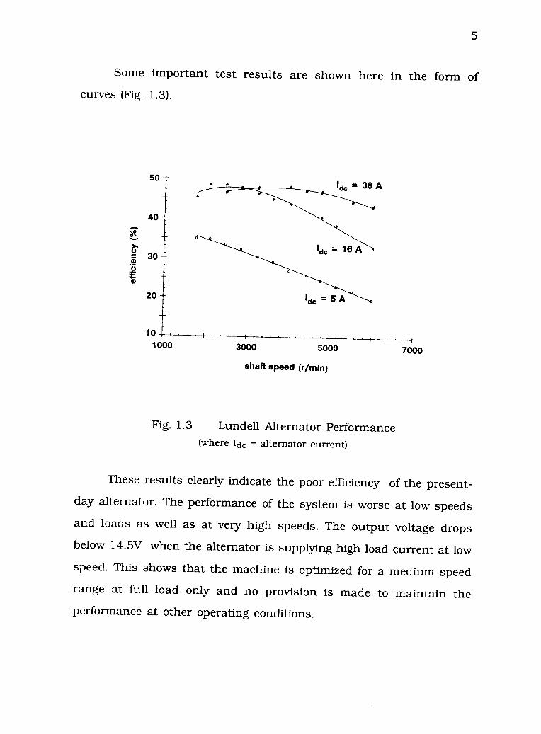
Some important test results are shown here in the form ofcurves (Fig. 1.3).
50
20 7
10 -
1000 3000 5000
shaft speed (r/min)
Fig. 1.3 Lundell Alternator Performance(where Ide = alternator current)
7000
These results clearly indicate the poor efficiency of the present-day alternator. The performance of the system is worse at low speedsand loads as well as at very high speeds. The output voltage dropsbelow 14.5V when the alternator is supplying high load current at lowspeed. This shows that the machine is optimized for a medium speedrange at full load only and no provision is made to maintain theperformance at other operating conditions.

6
The low efficiency of this present-day alternator has led to a re-examination of the automobile generator [1]. Highly-detailed, finite-element analyses are being applied to the improvement of the Lundellmagnetic circuit [2]. The findings of the work are probably moreappropriate to high per-unit cost aerospace generators than potentialimprovements to machines for automotive applications. It has beenproposed that a reduction of the speed range, by use of a gearbox oradjustable pulleys, should be used to improve the Lundell generatorefficiency [3]. However, these techniques, which are equally applicableto any variable speed generator, increase the system cost, reducereliability and introduce some control difficulties. More fundamental
improvements are possible if the Lundell generator is replaced by aninherently more efficient machine. For example, high efficiencyinduction machines are proposed as both the car engine starter (a lowspeed, high torque requirement) and the generator (a high speedvariable torque system). However, the required power conditioningunit (PCU) has a very high rating and is expected to result in anexpensive system in spite of being based on a robust, inexpensivemachine.
Finally, recent advances in permanent magnet materials haveresulted in high performance brushless d.c. motors which can beapplied to car generator and starter systems [4]. Most likely, thepermanent magnet a.c. generator will provide the best overallefficiency of any proposed system, because of zero excitationrequirements. This must be traded off against potentially prohibitivecapital costs caused by : (1) expensive magnet materials andconstruction cost; (2) large controllable power conversion unit and/or
7
gearbox required for voltage regulation. Problems have also beenreported with the mechanical, thermal and corrosion properties ofthe advanced permanent magnet materials.
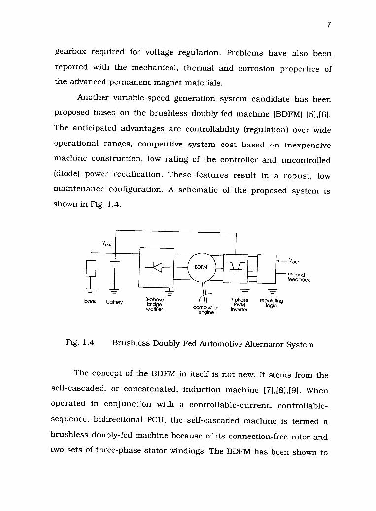
Another variable-speed generation system candidate has beenproposed based on the brushless doubly-fed machine (BDFM) [5],161.
The anticipated advantages are controllability (regulation) over wide
operational ranges, competitive system cost based on inexpensivemachine construction, low rating of the controller and uncontrolled
(diode) power rectification. These features result in a robust, lowmaintenance configuration. A schematic of the proposed system isshown in Fig. 1.4.
vout
loads battery 3-phasebridgerectifier combustion
engine
vout
--- secondfeedback
3-phase regulatingPWM logic
Inverter
Fig. 1.4 Brush less Doubly-Fed Automotive Alternator System
The concept of the BDFM in itself is not new. It stems from theself-cascaded, or concatenated, induction machine [7],[8],(91. When
operated in conjunction with a controllable-current, controllable-
sequence, bidirectional PCU, the self-cascaded machine is termed a
brushless doubly-fed machine because of its connection-free rotor andtwo sets of three-phase stator windings. The BDFM has been shown to
8
enable variable-speed generation (10) or adjustable speed drives tillwith only a small percentage of the total power being processed by itsPCU. Hence the PCU rating is small compared to that of the system,with the result that power electronic costs are significantly reduced.
Moreover, the performance of the machine can be controlled bymeans of three control variables : control winding voltage magnitude,frequency and phase sequence. These features of controlledoperational flexibility and potential competitive cost make the BDFMof interest for automotive applications. The BDFM is free from any sizelimitations both from the performance and manufacturing point ofview and thus appears to be an appropriate alternative, especially forhigh power ratings (3 to 5 kW in case of an automobile alternator).
The goal of this thesis work was to design and develop a PCUand a controller for output voltage regulation and alternator efficiencymaximization of the BDFM. Chapter 2 describes the design steps forthe PCU, a 3-phase PWM inverter. The rectifier design follows inChapter 3. The design of the voltage regulator and the efficiencymaximizer is explained in Chapter 4. Results from the laboratory testsperformed on the prototype alternator are presented in Chapter 5.Finally, conclusions and some recommendations for futureimprovements are presented in Chapter 6.

9
Chapter 2.
Design of a 3-Phase Pulse Width Modulated (PWM) Inverter
2.1 Selection of Inverter Topology
In the case of a BDFM system, the power conditioning unit(PCU) serves the purpose of supplying excitation to the controlwinding. The control winding is normally a balanced 3-phase, star-connected winding. In order to obtain maximum control over machineperformance, a variable-voltage and variable-frequency excitationsource is desirable.
In an automobile, the only source of electric power is thebattery, which can provide d.c. power. While the control winding canbe fed with d.c. power, this mode offers limited control and requires achopper for excitation control. Therefore, an inverter (for d.c. to a.c.conversion) is required to interface the battery with the controlwinding.
There are many choices available with regard to the type ofinverter such as a six-step or a square-wave switching inverter, a Pulse
Width Modulated (PWM) switching inverter, a resonant inverter,etc.In the case of a square-wave switching inverter, the output
frequency can be varied by controlling the switching instants; but theoutput voltage has to be controlled by controlling the input d.c. linkvoltage to the inverter. The control circuit is simple, resulting in alow-cost configuration. Switching losses are low, but the inverteroutput contains a significant amount of low order harmonics.
10
The control circuit of a PWM inverter is more complex, but itallows adjustment of both the output voltage magnitude and frequency.Also, by keeping the switching frequency high compared to thedesired output frequency, harmonics in the output can be pushed tohigher frequencies where filtering is easier because of the inductivenature of the load. The disadvantage of this scheme is higherswitching loss, which limits the switching frequency.
Resonant inverters are a relatively new class of inverters thatprovide for zero voltage and/or zero current switching of the powerdevices. This technique reduces the switching losses, thus enablinghigher switching frequencies and device utilization. The drawback ofthese topologies is the requirement of a resonant circuit and complexcontrol circuitry.
The proposed car alternator system requires a variable-voltage,variable-frequency inverter to act as an excitation source for thecontrol winding. Also, since the efficiency is an important aspect, lowharmonic content is desirable to avoid harmonic losses. Small sizerequirements mandate a compact power and control circuit with a lownumber of components. Therefore, the choice of a resonant converteris not justified, and a PWM inverter was chosen as a PCU. Of course, asix-step square wave output can also be obtained from the PWMinverter. Thus, the PWM inverter always allows the option of operatingin the square wave switching mode.

11
2.2 Automotive PWM Inverter Design Considerations
PWM inverters are perhaps the most widely used type ofinverter in industry. Nevertheless, the specific requirements of theBDFM alternator system necessitated the development of the inverterin-house rather than relying on an off-the-shelf design.
The application under consideration is a low-voltage, high-current application. The system voltage is normally 14.5V with some
transient variations, which may result in voltage spikes up to 20Vpeak. The maximum current drawn by the control winding of theexperimental machines was expected to be up to 20A rms at 9V (line)at approximately 0.5 p.f.
Normally, commercial inverters are designed for a high voltage(230/415 V) and a wide current range. Therefore, if a commercialinverter is to be selected for this application, it would be a mismatchwith regard to the voltage rating.
In order to develop an inverter for the prototype car alternator,full understanding of the device usage is required. This can beachieved with the developed inverter; since it provides access to allthe power devices for performance tests. Also, it is very easy toevaluate new power devices. Thus, optimum power device ratings forthe prototype can be determined with the help of the breadboardinverter.
The control circuit for the PWM inverter provides for easymodifications of the relevant parameters like switching frequency,mode of operation (square wave or PWM), and base driverequirements. This allows greater flexibility of operation.
12
The control circuit of this inverter consists of the minimumnumber of components for a sinusoidal PWM inverter. It becomesevident that the entire circuit can be put on a single chip once thecircuit parameters are determined after tests. Such devices,commercially known as 'smart power' devices, have been employed inthe case of power supplies and drives.
Since the inverter was developed in the laboratory usingrelatively inexpensive components, it allows easy and low costmaintenance, troubleshooting and modifications.
2.3 Power Circuit Design : Selection of Devices and Topology
Various types of power devices are commercially available forswitching applications like a PWM inverter.
Thyristors are inexpensive devices but impose a requirement offorced commutation. Gate Turn-Off thyristors (GTO's) are thyristorvariants which can be turned-off by means of gate control. But theamount of power required to initiate this gate turn-off is quiteconsiderable.
The Bipolar Junction Transistor (BJT) is a device that offersboth controlled switching 'on' and 'off. It is an inexpensive device andis simple to work with. It is a base-current-controlled device and is,therefore, relatively slow in switching operation. A BJT has very goodconduction characteristics but comparatively poor switchingcharacteristics.
The forward current gain (hfe) of a BJT can be enhanced byconnecting two or more devices in a Darlington configuration. This

13
increases the power handling capacity for the same base current, butreduces switching speed and also increases device losses.
Commercially, BJT's are available over a wide voltage and current
range and therefore provide good selection for optimization.
The Metal Oxide Semiconductor Field Effect Transistor(MOSFET) is a voltage controlled device. This device is best suited fora high frequency application and offers very good switchingcharacteristics. A positive temperature coefficient of resistance is animportant feature of a MOSFET that provides some safety and easyparalleling. The drain-to-source resistance, rds(on), is the parameterthat determines the forward voltage drop across the MOSFET during
conduction. Since this parameter is proportional to the die area it islow for high current devices, but can be considerable for low currentMOSFETs.
An Insulated Gate Bipolar Transistor (IGBT) is a relatively newdevice. It is most suitable in the medium frequency range (20kHz-
80kHz). Since it is a new device, it does not provide a wide range forselection and is available only in high voltage ratings. It also has aninherent problem of latch-up (a phenomenon when the gate losesturn-off control over the device) when it carries overcurrent.
This discussion indicates that a BJT or a MOSFET would be the
right candidate for this application. The MOSFET has an upper edgeover BJT so far as driving requirements are concerned. But moreimportant issues are cost and forward voltage drop. MOSFETs with low
current ratings would cause high voltage drop and those with highcurrent ratings would be expensive as well as over-rated devices forthis application. However, a very good selection of power BJT's is

14
available at the current and voltage ratings expected. These are lessexpensive and offer low forward voltage drop. Standard driver chipsare available for base drive circuit design. Also, no external free-wheeling diodes across the collector-emitter are required; since theseare integral in the transistor package.
The topology used for the inverter is the standard 3-leg topologywith two devices in each leg. In order to simplify drivingrequirements, it is essential to use complementary devices in each leg.PNP transistors are used as top transistors and NPN transistors areused as bottom transistors as shown in Fig. 2.1.
Vdc
Fig. 2.1 Three Phase PWM Inverter
ABC
This arrangement eliminates the need of isolated power suppliesfor the top and bottom transistor base-drive circuitry. Withcomplementary devices, when the base drive circuit of the toptransistor (PNP) drives its base to ground, the transistor startsconducting and goes into saturation. When the base is connected tothe d.c. link voltage the transistor turns 'off. The base drive circuit hasfull control over the base current and the load voltage does not affect

15
the base current. The rating of the PNP transistor needs to be same asthat of the bottom NPN transistor.
A prototype Brush less Doubly-Fed Automotive Alternator (BDFAA)
was designed [6] for proof-of-concept-type tests. The machine has two
isolated stator windings in the same stator frame. The power winding
is wound for six poles and the control winding for two poles. The rotor
has a nested loop structure. There are four nests with three loops in
each nest forming a cage like rotor structure.
The maximum control winding current was estimated to be 20A
(rms) using computer simulation data and applying reasonable limits.
This calls for a device with approximately 28A (\12 *20) currentcarrying capacity, which warrants the choice of a BJT with lc = 30A.
The system voltage is about 20Vdc maximum. Therefore the BJTshould have a minimum of 20V forward blocking capacity. (i.e. Vceo =
20V min.)
These two are the most important ratings which can be used for
device selection. To satisfy these, Motorola MJ11011 PNP andMJ11012 NPN, Darlington power transistors were selected (refer toAppendix I for the data sheets). These devices have 30A collector
current-carrying capacity and a voltage rating of 60V. This allows for
some safety margin. Another device aspect to be examined is the
Forward Bias Safe Operating Area (FBSOA). The FBSOA for switching or
pulsed operation is normally larger than the FBSOA for d.c. operation
(almost rectangular) because the device is capable of conducting heatduring the 'off period.
'On' voltages characteristics show that the collector-to-emittervoltage drop is low when the device is 'on'. This is a critical parameter
16
for automotive applications because the d.c. link voltage is regulated to14.5 VDC. This mandates the use of low-voltage-drop devices to obtain
maximum voltage output. The d.c. current gain of the device (the ratioof collector current to base current) is 500 (minimum) for 30A(maximum) collector current. This implies that a base current of60mA minimum is required to keep the device in saturation over theentire current range. In practice, a higher value of base current isapplied.
The devices have a built-in free-wheeling diode across thecollector-emitter which is required as the load has an inductivenature. These diodes allow two-quadrant operation of the inverter i.e.the inverter can support forward motoring as well as regeneration. Inother words, the active power flow can be from the battery to thecontrol winding or vice versa if the control winding starts generating.This is an important feature which is utilized for efficiencymaximization.
2.4 Inverter Control Circuit
The complete inverter control circuit can be grouped into threecontrol units, which are functionally separate but are interdependentas shown in Fig. 2.2.
The control circuit that generates the actual PWM switchingpattern is henceforth referred to as the Switching Pattern Generator(SPG). In order to maintain the output voltage at 14.5 VDC, a VoltageRegulator Circuit (VRC) is required. Moreover, to achieve the

17
maximum efficiency of operation, an Efficiency Maximizer Unit (EMU)unit is necessary.
Power Circuit SPG
VoltageControl
Switching FrequencyPulses Control
VRC 1.4
EMU
OutputVoltage
Fig. 2.2 Controller Block Diagram.
EngineSpeed
This section discusses the design and development of the SPG.The design of VRC and EMU follows in Chapter 4.
Numerous techniques are available to generate the switchingpattern for a 3-phase PWM inverter. Sinusoidal PWM (SPWM) isperhaps the simplest method and is thoroughly discussed in theliterature [12]. It can be easily implemented using analog components.The digital counterpart of this scheme involves asymmetrical orsymmetrical sampling of the modulating wave [13]. With advancementsin microprocessor technology, the use of microprocessors to generateswitching patterns is also increasing [13]. Some other methods areselective harmonic elimination schemes [14], adaptive or hysteresiscontrol [15], and space vector techniques [16] .
However, for this application, the natural SPWM technique wasselected because of its well-established, simple and very flexiblenature. It can be implemented using a few low-cost components, while

18
still enabling good performance. The circuit, being mostly analog, canvery well withstand the noisy environment (Electro-MagneticInterference (EMI) from spark-plugs, solenoid switchings, etc.) in anautomobile.
The technique employs a comparison of a high frequencytriangular wave and a sine wave to obtain the switching instants asshown in Fig. 2.3 [12].
ucontrol
'Jo
0
Vol
Fig. 2.3 Sinusoidal PWM Technique.
(From 'Power Electronics: Converters, Applications and Design' : Ned
Mohan et al.)
where,
vcontrol
vtri
Vo
: modulating voltage waveform
: carrier voltage waveform
: instantaneous output voltage waveform
19
vol : output voltage fundamental component
Vd : d.c. link voltage
The triangular wave, also referred to as the carrier wave, decidesthe switching frequency. The output voltage magnitude and frequencydepends upon the amplitude and the frequency of the sine wave or themodulating wave. In case of a 3-phase PWM inverter, only one carrierwave is sufficient but three sine waves displaced by 1200 are requiredas modulating waveforms.
The ratio of the modulating wave amplitude to the carrier waveamplitude is known as Amplitude Modulation Ratio (Ma). The ratio ofthe carrier wave frequency to the modulating wave frequency is knownas Frequency Modulation Ratio (Mf). Fig. 2.4 [12] shows the inverteroutput line voltage harmonic spectrum for a high Mf. Fig. 2.5 [12]shows the ratio of inverter output line voltage to the d.c. link voltage asa function of Ma (for an ideal case).
1.0
0.8
0.6
0.4
0 21-t1 t\x
mf 2m1(Mr +
ma = 0.8, mf = 15
tl
(2m1 + 1)
Harmonics of fi
3m1f
(3m1 + 2)
Fig. 2.4 Output Voltage Harmonic Spectrum(From 'Power Electronics: Converters, Applications and Design' : Ned
Mohan et al.)

(rms)
V d
Square-wave
= 0.612 --2,, 2
Linear
OvermodulationSquare-wave
3.24(for mf = 15)
20
Fig. 2.5 Output Voltage Vs. Ma
(From 'Power Electronics: Converters, Applications and Design' : Ned
Mohan et al.)
A hybrid (digital and analog) circuit [17] is developed to generatethese waveforms, which are used to obtain the PWM switching pattern.Fig. 2.6 shows the scheme in a block-diagram form. For detailedcircuit diagram refer to Appendix II.
FrequencyControlInput
21
Carrier WaveGenerator
3 Phase SineWave Generator
VoltageControl
Input
Multi-pliers
Compa-rators
BlanldngTimeAdders
Opto-isolators
DriversPowerCircuit
Fig. 2.6 PWM Pattern Generator (SPG).
A Digitally Controlled Analog Switch (DCAS), an integrator and aSchmitt trigger form a closed loop circuit to generate a triangularcarrier wave and a square wave, the frequency of which depends upona voltage reference input signal. The square wave is then passedthrough a frequency divider and flip-flops to generate a low frequency3-phase square wave. In turn, the square waves are used to generatethree triangular waves of constant amplitude. Three 'FET sine-shaper'circuits then shape these triangular waves into sine waves, which aresubsequently multiplied by the amplitude reference voltage signal.
Thus, the triangular carrier wave and the three sinusoidalmodulating waves are now available. Fig. 2.7 shows a plot of thesewaveforms obtained in the laboratory.

22
-50.0000 es 0.00000 s
10.0 ssidivfrequency( 1 ) 49,1176 Hz frequency( 4 ) 49.1/77 Irzfrequency( 3 ) 49,1176 16
50.0000 es
hp stopped
more presetprobe
CHANNEL
2 3 4
C
5.00 V/div
-10.0000 is 0.00000 s
2.00 esidlyfrequency 1 ) not found frequency( 2 , not foundtrequenc0 3 not found frequency, 4 not found
10,0000 es
0 00000
de5H lie
cc
more presetprops
Fig. 2.7 Modulating and Carrier Waveforms
(vertical scale : 2V/div for top plot and 5v/div for bottom plot)
Operational-amplifier (Op-amp) comparators are employed togenerate the switching pattern through a comparison of the carrierwave and each of the three modulating waves. The pulses obtained are

23
then passed through a blanking-time addition circuit, which is nothingbut a polarized RC network. The blanking time prevents theoccurrence of any shoot-through fault. The RC circuit is followed by aSchmitt trigger which is required to restore the rectangular shape ofthe pulses. These pulses are then fed to the opto-isolators, whoseoutputs are connected to the driver chip. The driver chip outputsdrive the base terminals of the bottom (NPN) transistors directly.However, the base terminals of the top (PNP) transistors are driventhrough base drive transistors, in order to perform the necessaryinversion.
2.5 Inverter Performance
The performance of the inverter is determined by testing it forefficiency and output harmonic spectra.
Assuming ideal switches as well as ideal circuit conditions andsinusoidal output waveforms, the input-output equation for an invertercan be written as:
1Vdcl NJ = N/3 Mil [ Iiil [ cost) 1 (2.5-1)where,
Vdc : D.C. link voltage.
Idc : D.C. link current.
VII : Inverter output voltage (line-to-line).
Iii : Inverter output current (line-to-line).
coso : load power factor.
In a practical situation, the switches are not ideal, but haveswitching and conduction power loss associated with them. Also, the
24
harmonics in the output voltage and current waveform reduce theuseful output power, as only the fundamental of the voltage andcurrent convey the useful power. The inverter control circuit and thebase-drive circuit for the power transistors also consume some power.All these factors bring down the inverter efficiency.
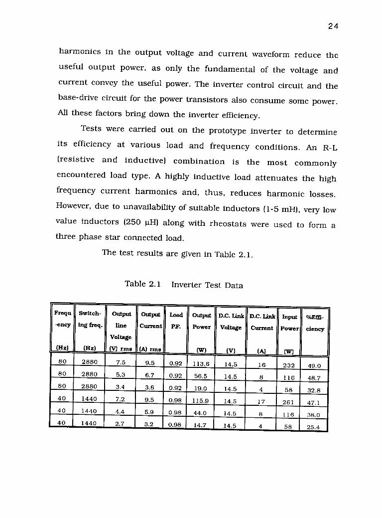
Tests were carried out on the prototype inverter to determineits efficiency at various load and frequency conditions. An R-L(resistive and inductive) combination is the most commonlyencountered load type. A highly inductive load attenuates the highfrequency current harmonics and, thus, reduces harmonic losses.However, due to unavailability of suitable inductors (1-5 mH), very lowvalue inductors (250 pt.H) along with rheostats were used to form athree phase star connected load.
The test results are given in Table 2.1.
Table 2.1 Inverter Test Data
Frequ
-ency
(Hz)
Switch-
ing freq.
(Hz)
Output
line
Voltage
(V) rms
Output
Current
(A) rms
Load
P.F.
Output
Power
(W)
D.C. Link
Voltage
(V)
D.C. Link
Current
(A)
Input
Power
(W)
%Effi-
ciency
80 2880 7.5 9.5 0.92 113.6 14.5 16 232 49.080 2880 5.3 6.7 0.92 56.5 14.5 8 116 48.780 2880 3.4 3.6 0.92 19.0 14.5 4 58 32.840 1440 7.2 9.5 0.98 115.9 14.5 17 261 47.140 1440 4.4 5.9 0.98 44.0 14.5 8 116 38.040 1440 2.7 3.2 0.98 14.7 14.5 4 58 25.4
25
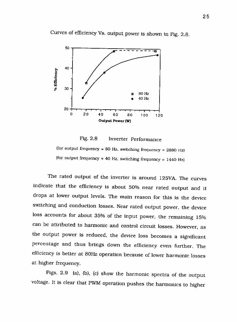
Curves of efficiency Vs. output power is shown in Fig. 2.8.
20 .. 1 .. , .. 1 . 1 .. 1 "0 20 40 60 80 100 120
Output Power (W)
Fig. 2.8 Inverter Performance
(for output frequency = 80 Hz, switching frequency = 2880 Hz)
(for output frequency = 40 Hz, switching frequency = 1440 Hz)
The rated output of the inverter is around 125VA. The curvesindicate that the efficiency is about 50% near rated output and itdrops at lower output levels. The main reason for this is the deviceswitching and conduction losses. Near rated output power, the deviceloss accounts for about 35% of the input power, the remaining 15%can be attributed to harmonic and control circuit losses. However, asthe output power is reduced, the device loss becomes a significantpercentage and thus brings down the efficiency even further. Theefficiency is better at 80Hz operation because of lower harmonic lossesat higher frequency.
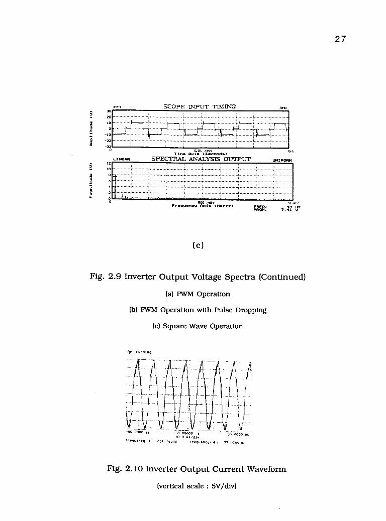
Figs. 2.9 (a), (b), (c) show the harmonic spectra of the outputvoltage. It is clear that PWM operation pushes the harmonics to higher

26
frequencies. The square-wave-mode of operation introduces a
significant amount of lower order harmonic but, at the same time,
provides a higher fundamental voltage component. Fig. 2.10 is a
sample output current waveform when the inverter is operated in thePWM mode.
30
20
71'
z
10
-10
-20
300
5
3
2
0
30
20
10
0
-10
-20
300
12
10
6
4
2
0
FFT SCOPE INPUT TIMING CHL
LINEAR
0.01 AJ1VTina Axis (Seconds)
SPECTRAL ANALYSIS OUTPUT0.1
UNIFORM
1
5E+03
MR: 5.2 tiz
FFT
500 /ctivFrequency Axis (Hertz)
(a)
SCOPE INPUT TIMING CHI
LINEAR
0.01 /111VTina Axis (Seconds)
SPECTRAL ANALYSIS OUTPUT0.1
UNIFORM
500 /et',Frequency Axis (Hertz)
(b)
5E+0349
6.89 U.
Fig. 2.9 Inverter Output Voltage Spectra
(a) PWM Operation
(b) PWM Operation with Pulse Dropping
(c) Square Wave Operation
30
20
10
0
-10
-20
-300
FFT
27
SCOPE INPUT TIMING CHI
LINEAR12
10
6
4
2
00
0.01 /divTi.,. Axis (Seconds)
SPECTRAL ANALYSIS OUTPUT0.1
UNIFORM
500 ,d1nFres:sue:new Axis (Hertz)
(c)
nFNEGgi5E003
7.21 V
Fig. 2.9 Inverter Output Voltage Spectra (Continued)
(a) PWM Operation
(b) PWM Operation with Pulse Dropping
(c) Square Wave Operation
-50 0000 es 0 00000 s 50 0000 es10 0 es/d10
frequency( I not found frequency( 4 77 0769 16
Fig. 2.10 Inverter Output Current Waveform
(vertical scale : 5V/div)
28
Chapter 3.
Design of 3-Phase Power Rectifier
3.1 Device Selection and Design
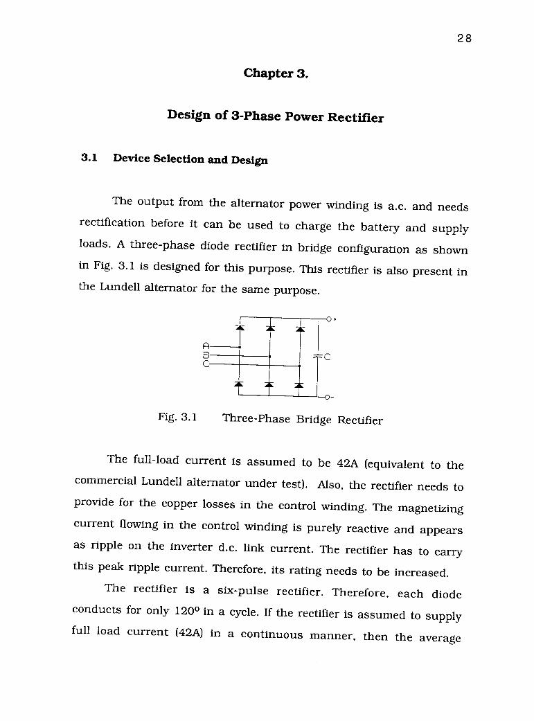
The output from the alternator power winding is a.c. and needsrectification before it can be used to charge the battery and supplyloads. A three-phase diode rectifier in bridge configuration as shownin Fig. 3.1 is designed for this purpose. This rectifier is also present inthe Lundell alternator for the same purpose.
Fig. 3.1 Three-Phase Bridge Rectifier
The full-load current is assumed to be 42A (equivalent to thecommercial Lundell alternator under test). Also, the rectifier needs toprovide for the copper losses in the control winding. The magnetizingcurrent flowing in the control winding is purely reactive and appearsas ripple on the inverter d.c. link current. The rectifier has to carrythis peak ripple current. Therefore, its rating needs to be increased.
The rectifier is a six-pulse rectifier. Therefore, each diodeconducts for only 120° in a cycle. If the rectifier is assumed to supplyfull load current (42A) in a continuous manner, then the average
29
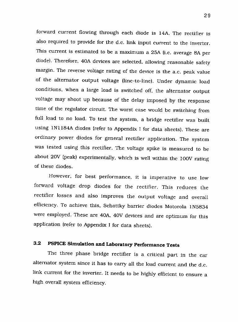
forward current flowing through each diode is 14A. The rectifier isalso required to provide for the d.c. link input current to the inverter.This current is estimated to be a maximum a 25A (i.e. average 8A per
diode). Therefore, 40A devices are selected, allowing reasonable safety
margin. The reverse voltage rating of the device is the a.c. peak valueof the alternator output voltage (line-to-line). Under dynamic loadconditions, when a large load is switched off, the alternator outputvoltage may shoot up because of the delay imposed by the responsetime of the regulator circuit. The worst case would be switching fromfull load to no load. To test the system, a bridge rectifier was builtusing 1N1184A diodes (refer to Appendix I for data sheets). These areordinary power diodes for general rectifier application. The systemwas tested using this rectifier. The voltage spike is measured to beabout 20V (peak) experimentally, which is well within the 100V ratingof these diodes.
However, for best performance, it is imperative to use lowforward voltage drop diodes for the rectifier. This reduces therectifier losses and also improves the output voltage and overallefficiency. To achieve this, Schottky barrier diodes Motorola 1N5834
were employed. These are 40A, 40V devices and are optimum for thisapplication (refer to Appendix I for data sheets).
3.2 PSPICE Simulation and Laboratory Performance TestsThe three phase bridge rectifier is a critical part in the car
alternator system since it has to carry all the load current and the d.c.link current for the inverter. It needs to be highly efficient to ensure ahigh overall system efficiency.
30
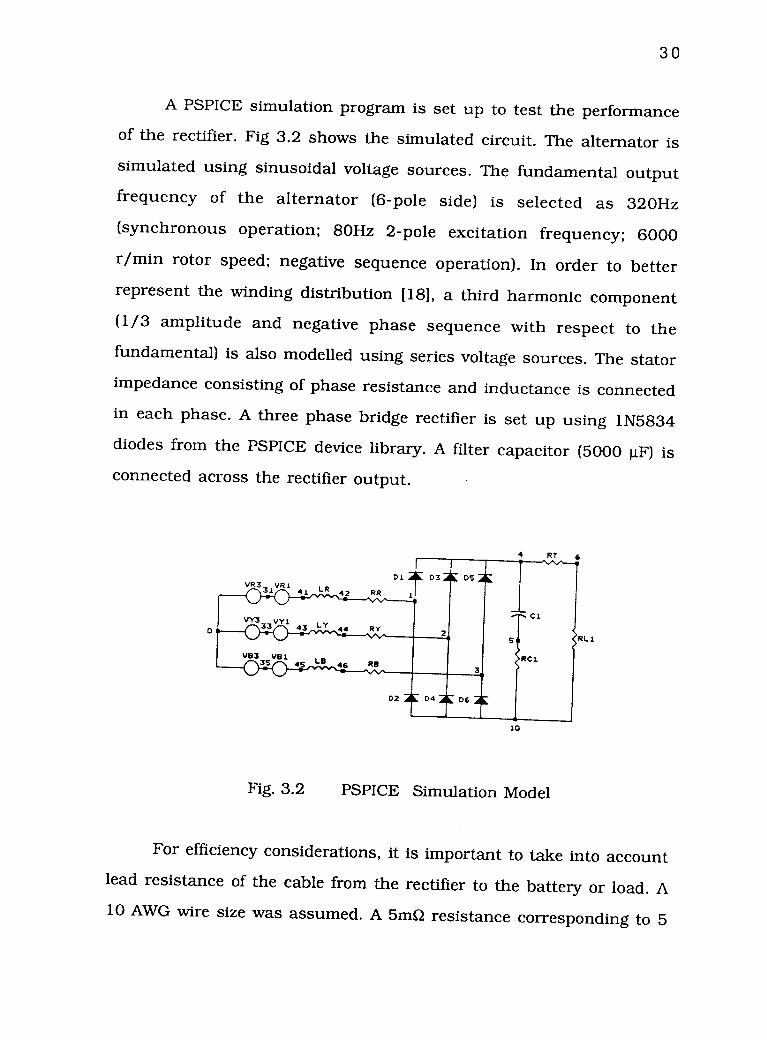
A PSPICE simulation program is set up to test the performanceof the rectifier. Fig 3.2 shows the simulated circuit. The alternator issimulated using sinusoidal voltage sources. The fundamental outputfrequency of the alternator (6-pole side) is selected as 320Hz(synchronous operation; 80Hz 2-pole excitation frequency; 6000r/min rotor speed; negative sequence operation). In order to betterrepresent the winding distribution [181, a third harmonic component(1/3 amplitude and negative phase sequence with respect to thefundamental) is also modelled using series voltage sources. The statorimpedance consisting of phase resistance and inductance is connectedin each phase. A three phase bridge rectifier is set up using 1N5834diodes from the PSPICE device library. A filter capacitor (5000 j.tF) isconnected across the rectifier output.
10
Fig. 3.2 PSPICE Simulation Model
For efficiency considerations, it is important to take into accountlead resistance of the cable from the rectifier to the battery or load. A10 AWG wire size was assumed. A 5mi2 resistance corresponding to 5

31
feet of cable was added to the circuit. The stator-side cable resistancewas neglected; since the rectifier is placed very close to the statorwinding during normal operation.
The rectifier was tested for 20A and 40A load currents. The loadwas simulated using a resistor.
To compare the simulation results and actual performance, thesimulation program is also run with 60Hz voltage sources feeding therectifier. The rectifier is tested in the laboratory for 60Hz operation,with a three phase autotransformer feeding the a.c. side of therectifier. The filtered output is connected to rheostats forming theload. The simulation results and the test results for 60Hz as well as320Hz operation are summarized in Table 3.1.
Table 3.1 Rectifier Test Data
Simulation Results Test Results
Freq-
ency
(Hz)
Load
Current
(A)
Load
Voltage
(V)
Input
Power
(W)
% Effici-
ency
Input
line
Voltage
(V) rms
Input
Current
(A) rms
Power
Factor
v
% Effici-
ency
60 20 14.5 300 96.7 12.4 15.0 0.94 96.060 40 14.5 638 90.9 13.6 29.0 0.95 89.5
320 20 14.5 305 95.1 12.8 14.6 0.94 95.4320 40 14.5 642 90.3 N/A N/A N/A N/A
where,
0/0 Efficiency 100 [Output Power / Input Power]

32
Output Power = [Load Voltage] [Load Current]
Input Power = 13 [Input Voltage] [Input Current] [Power
Factor]
In order to calculate the rectifier efficiency, only input powerand output power are required. With PSPICE, it is convenient tocompute the input power by adding the instantaneous powerwaveforms of the three phases and then taking the average of theresultant waveform rather than determining the input power using thecurrent and voltage true RMS values which are not easily available. Forlaboratory tests, a power profiler was used which provides the poweras well as true RMS voltage and current values with power factor.These figures are included in the table to give a better idea of themagnitudes of voltage and current involved.
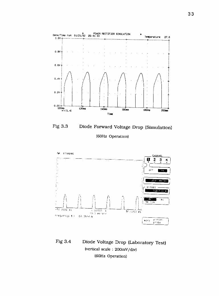
A simulation plot for the diode forward voltage drop for 40A load
current is shown in fig. 3.3. Actual diode forward voltage drop for 40Aload current is shown in Fig. 3.4, a plot obtained during the laboratorytests.
POWER RECTIFIER SIMULATIONDate/Time run: 01/21/92 20: 41: 33 Temperature: 27.01.0V+ 4- -+ 4- -4-
0.8V+
0.6V+
0.4V+ .
0.2V +
0.0V +100ms
*v (1,4)
4-120ms 140ms
Time
160ms-+
180ms 200ins
Fig 3.3 Diode Forward Voltage Drop (Simulation)
(60Hz Operation)
/np s toppedrHANNEL
( a 2 3 4 1Ito o of,Th(
imia
2'C luV
0 T f se t
75a. tll.L,:l ,Il '.
ac
f requeriCg( 1 50 36
Fig 3.4
I Oce.e tpr °tie
Diode Voltage Drop (Laboratory Test)(vertical scale : 200mV/div)
(60Hz Operation)
33

34
The simulation results and the test results closely match. Therectifier efficiency is quite high aiding the efficient operation of thealternator system. However, it should be noted that the simulation iscarried out at 270C; rectifier losses will increase for operation athigher temperature, thus decreasing the efficiency. The model can beused to predict the performance at higher temperatures by using the'.TEMP' command.

35
Chapter 4Design of Voltage Regulator and Efficiency Maximizer
4.1 Design of the Voltage Regulator
A recommended practice [191 is that the car alternator shouldbe capable of maintaining 14.5V while delivering the full-load current(i.e. 42A in the case of the tested commercial alternator). As in thecase of any alternator, in the absence of a regulator, the output voltagewould drop with increase in load current. The main reason for this isthe voltage drop in the winding itself. Therefore, it becomes necessaryto boost the generated internal e.m.f. to compensate for this drop.This can be achieved by increasing the excitation or the field current,assuming a constant speed of operation.
In the case of the BDFAA, the excitation can be controlledthrough the inverter feeding the control winding. The d.c. link of theinverter is the d.c. bus across which the battery and the other loadsare connected. The inverter output voltage and frequency bothdetermine the control winding current. If the frequency is assumed tobe constant, the excitation depends solely on the inverter outputvoltage. For simplicity, the following discussion assumes a constantinverter output frequency. It is also assumed that the d.c. link voltagestays constant at 14.5V and the machine can support full load currentat the assumed excitation frequency; i.e. the impedance of the controlwinding is such that enough excitation current can be supplied withthe inverter output line voltage limited to about 9V. The implicationsof these assumptions are explained later in this section.

36
The control strategy employed to regulate the inverter outputvoltage and hence, the alternator output voltage, is standard outputfeedback control. Fig. 4.1 shows the Voltage Regulator Circuit (VRC)scheme in block diagram form. A detailed circuit diagram can befound in Appendix II.
ReferenceVoltage +
InstrumentationAmplifier Error Amplifier
ErrorVoltage
Integrator
SystemVoltage
VoltageControlInput
Fig. 4.1 Voltage Regulator
(The 'Voltage Control Input' goes to SPG (Fig. 2.6))
A reference corresponding to 14.5V is set up using an auxiliarypower supply. In a practical automotive application, this may not bepossible and a reference voltage using a zener diode may have to begenerated. The system voltage is also properly scaled using a potentialdivider. The calibration procedure simply involves adjusting thepotential divider such that the error between the reference voltageand the scaled system voltage is reduced to zero when the systemvoltage is 14.5V. An error amplifier circuit is used to amplify any errorthat occurs during normal operation. The error signal is then fed to a
37
Proportional-Integral (PI) controller. An op-amp integrator [20]performs the necessary integration. The output of the PI controller is
connected to the multiplier circuits in the SPG. Thus, the output ofthe PI controller controls the amplitude of the three reference sinewaves and hence the inverter output voltage.
A pure proportional control causes severe output voltageoscillations under load conditions. Therefore, PI control is required. A
step increase in load current causes a dip in system voltage, resultingin a step change in the error amplifier output, i.e. the PI controllerinput. The PI controller then ramps up the inverter output voltage and
brings the system voltage back to 14.5V. When the error reduces tozero, the output of the PI controller stays constant, thus maintaining
the output voltage and current. As the battery is being charged, thevoltage tends to rise above 14.5V, causing negative error. This slowlybrings down the PI controller output until the voltage remains steadyat 14.5V. These oscillations are very small (within 0.1V), and finally
the system settles to 14.5V with constant inverter output.
A step reduction in load current causes a momentary rise in the
system voltage, producing a large negative error at the PI controllerinput. This would cause the PI controller output to swing negative.However, multiplier circuits perform multiplication of the inputmodulus only. Therefore, a diode is connected at the PI controlleroutput to block the negative input to the multipliers. In such a case, azero input to the multipliers brings down inverter output to aminimum. This reduces the system voltage back to 14.5V.
The integral control reduces the steady state error to zero and itcan easily be adjusted to obtain very low overshoots. But the response
38
is slightly sluggish. The gains need to be adjusted such that theresponse is fast enough for large load changes. This is especially true
for a sudden load increase. If the response is not fast enough, thebattery starts discharging and the system voltage can drop to a verylow value (less than 10V). This results in a reduced d.c. link inputvoltage to the inverter, causing reduced inverter output voltage. With
reduced excitation, the system voltage drops further and systemoutput decays beyond recovery. However, this behavior is the result ofthe initial assumption of constant speed and frequency.
One possible way to avoid this system crash is to increase thespeed of rotation to enhance generation at the same excitation level.
But this is not practical; since the engine speed would be decided bythe driver and cannot be changed to meet the alternatorrequirements.
System voltage response to step increases in load can also becontrolled by reducing the inverter output frequency. This reduces theimpedance of the control winding, allowing more excitation current toflow for a given inverter output voltage. Increased excitation in turnincreases the output voltage and the system can recover. This action istaken by the EMU and is explained in more detail in Section 4.3.
4.2 Performance Tests on VRC
The dynamic performance of the VRC is tested by subjecting the
prototype alternator system to a step change in load current from noload to 25A. Standard control system parameters [21] are measuredfrom the response obtained. Fig. 4.2 shows the plot of the system
39
voltage (trace A) and the regulator output voltage(trace B). Theglitches in the waveforms are because of the pick-up duringmeasurements.
StoppedCHANNEL
ill 2 3 40 0
1(off
6,.56(f .
0.00000 s 50.0000 ms10.0 ms/div
100.000 MS
ac
1 morepresetprobe
Fig. 4.2 VRC Performance(Trace A : system voltage waveform)
(Trace B : regulator output voltage waveform)
(vertical scale : 2V/division)
The system voltage is seen to drop for some time after theapplication of load at to. Then the regulator starts correcting theerror at time t1. However, because of a delay caused by the SPG andvarious inductances, the output voltage continues to drop for somemore time, until t2, and reaches a low of approximately 9V .
Thereafter, because of the increased inverter output, the outputvoltage starts recovering and comes back to 14.5V at t3.
The 'delay time (td)' of the system, defined as the time requiredfor the step response to reach 50% of its final value, is 40ms. The 'rise
40
time (tr)', defined as the time required for the step response to risefrom 10% to 90% of its final value, is 30ms. The 'settling time (ts)' ofthe system, defined as the time required for the step response to staywithin a specified percentage (5%, in case of an automotive alternator)of its final value, is 80ms. For an automotive application this recoveryis fast enough. Also, it can be seen that there is no overshoot,indicating that the system is well-damped.
The performance of the prototype system is found to besatisfactory for all load changes up to a maximum of 25A with thealternator running at 6000 rev/min. At lower speeds the maximumoutput current capability of the alternator reduces. If a load higherthan 25A is applied the system voltage drops and stays at some valuelower than 14.5V.
4.3 Efficiency Maximizer Unit (EMU)
The conventional Lundell alternator has no provision forimproving the efficiency at any operating point, since the only control
variable, the field current, is used for output voltage control. However,in the case of a BDFAA, two control variables are available. As discussedin Section 4.1, the inverter output voltage is utilized to control thesystem voltage. This leaves the other variable, i.e. the inverter outputfrequency, free for efficiency improvement. The inverter outputfrequency can be controlled by controlling the voltage level at the'Frequency Control Input' of the SPG (Fig. 2.6). The phase sequence ofthe inverter output can also be controlled.

41
In order to understand the efficiency maximization principle, itis necessary to examine the field relationships in a BDFM. Fig. 4.3shows the relative directions and velocities of the fields existing in aBDFM.
Fig. 4.3 Field Relationships
where,
fp : power winding frequency
Pp number of power winding pole pairs
fpr : power winding induced rotor frequency
Ns : rotor angular velocity (rev/s)
fc : control winding frequency
fcr : control winding induced rotor frequency
Pc : number of control winding pole pairs
and for synchronous operation fpr = fen
For normal generator operation, the power winding field rotatesin the same direction as the rotor. However, the control windingexcitation phase sequence can be adjusted; therefore, the controlwinding field can rotate in either direction. The phase sequencewhich causes the control winding field to rotate in the opposite
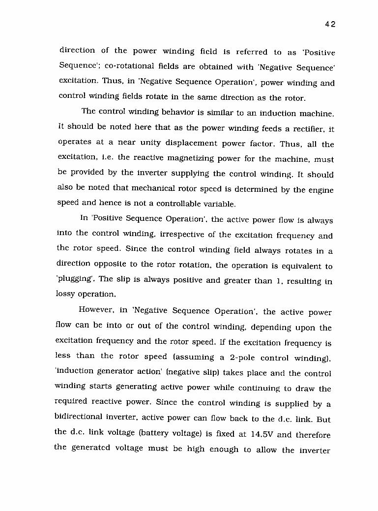
42
direction of the power winding field is referred to as 'PositiveSequence'; co-rotational fields are obtained with 'Negative Sequence'
excitation. Thus, in 'Negative Sequence Operation', power winding and
control winding fields rotate in the same direction as the rotor.
The control winding behavior is similar to an induction machine.It should be noted here that as the power winding feeds a rectifier, itoperates at a near unity displacement power factor. Thus, all theexcitation, i.e. the reactive magnetizing power for the machine, mustbe provided by the inverter supplying the control winding. It shouldalso be noted that mechanical rotor speed is determined by the enginespeed and hence is not a controllable variable.
In 'Positive Sequence Operation', the active power flow is always
into the control winding, irrespective of the excitation frequency andthe rotor speed. Since the control winding field always rotates in adirection opposite to the rotor rotation, the operation is equivalent to'plugging'. The slip is always positive and greater than 1, resulting inlossy operation.
However, in 'Negative Sequence Operation', the active powerflow can be into or out of the control winding, depending upon theexcitation frequency and the rotor speed. If the excitation frequency isless than the rotor speed (assuming a 2-pole control winding),'induction generator action' (negative slip) takes place and the controlwinding starts generating active power while continuing to draw therequired reactive power. Since the control winding is supplied by abidirectional inverter, active power can flow back to the d.c. link. Butthe d.c. link voltage (battery voltage) is fixed at 14.5V and thereforethe generated voltage must be high enough to allow the inverter

43
diodes to conduct. Whether the control winding would be able to
charge the battery or not depends on various factors like machine
parameters, the load on the battery, excitation frequency and voltage,
rotor speed, etc. But it is clear that the 'Negative Sequence Operation'
of the prototype alternator promises a way to improve the overall
system efficiency by means of power generation using both windings.
However, the desired 'induction generator' action imposes an upper
limit on the control winding excitation frequency. An engine speed
feedback is thus desirable to minimize the search time for the bestefficiency point.
Also, in order to keep the copper losses in the control winding
to a minimum, the excitation current should be reduced to a
minimum. This can be achieved by increasing the excitation frequency.
The frequency can be increased so long as enough voltage is available
at the inverter output to supply the minimum required excitation.
Once the maximum inverter output voltage is reached (limited by the
d.c. link), any increase in frequency will result in a reduction ofexcitation current below the required minimum. In turn, this willcause a reduction of alternator output voltage.
Thus, it can be seen that in the case of the prototype alternator,
the EMU needs to be sensitive to rotor speed variations caused by
engine speed changes and system voltage variations because of load
changes. Using a 'Negative Sequence Operation', the EMU has to
generate a 'Frequency Control Input' for the SPG. This signal should be
such that the excitation frequency causes the maximum possible active
power flow out of the control winding, corresponding to the operating
point. However, under some load and speed conditions, it may not be

44
possible to achieve power flow out of control winding. Under these
circumstances, the EMU should lower the excitation frequency justenough to maintain the alternator output voltage.
A flow-chart describing the EMU operation is shown in Fig. 4.4.
Engine Speed Feedback
Reference Frequency Output
Output Voltageless than 14.5 ?
Raise the Frequ-ency Reference
Lower the Frequ-ency Reference
Fig. 4.4 EMU Operation
A simple electronic circuit designed to accomplish thisoperation is shown in Appendix II. The scheme uses both the speedfeedback as well as the output voltage feedback and generates a'Frequency Control Input' signal for the SPG. In a practical automotiveapplication, the engine speed information can be obtained using the'timing signals' generated for the electronic fuel injection system.However, this requires additional external wiring into the alternator

45
casing. A better approach, which avoids this, is suggested in Section
6.2.
In order to illustrate the efficiency maximization principle, the
alternator is run at an approximately constant speed, 6100 rev/min.
(101 rev/s). The system voltage is maintained at 14.5V and a 25A load
is connected (constant electrical output power, 362.5W). The inverter
output frequency is varied over a range and the results are shown in
Table 4.1.
Table 4.1. Efficiency Maximization Test
(constant electrical output power = 362.5W)
Alt.
torque
(N-m)
Mech.
power
(W)
2-pole
frequency
(Hz)
6-pole
frequency
(Hz)
2-pole
rms line
voltage
(V)
2-pole
rms
current
(A)
D.C. link
current
(A)
%
Efficiency
2.1 1312.8 55 348 10.5 18.8 11.5 27.6
1.8 1179.6 60 345 11.4 17.2 8.1 30.7
1.6 1042.3 66 338 12.3 14.9 3.4 34.8
1.4 902.3 74 330 13.2 12.8 -1.8 40.2
where, % Efficiency = 100 [Mechanical Power / Electrical Power]
It can be seen that as the 2-pole (inverter output) frequency is
increased, the 2-pole current reduces and so does the alternator input
torque. Thus, while maintaining constant electrical output power, the
mechanical input power decreases and the system efficiency is
improved. The best efficiency is obtained at 74Hz, when the 2-pole
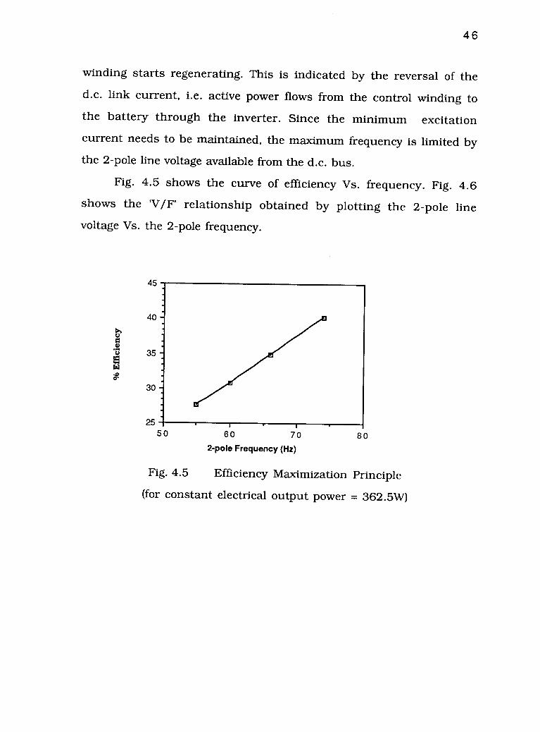
46
winding starts regenerating. This is indicated by the reversal of thed.c. link current, i.e. active power flows from the control winding to
the battery through the inverter. Since the minimum excitationcurrent needs to be maintained, the maximum frequency is limited bythe 2-pole line voltage available from the d.c. bus.
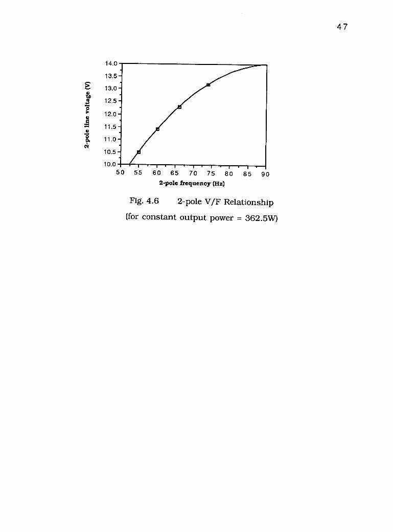
Fig. 4.5 shows the curve of efficiency Vs. frequency. Fig. 4.6shows the 'V/F' relationship obtained by plotting the 2-pole linevoltage Vs. the 2-pole frequency.
45
40
35 7
30 -
2550 60 70
2-pole Frequency (Hz)
80
Fig. 4.5 Efficiency Maximization Principle
(for constant electrical output power = 362.5W)
14.0 -
13.5 -
13.0 -
12.5 -
12.0 -
11.5-
11.0 -.
10.5 -. /11/7171 1 1 1 1 1 110.0
50 55 60 65 70 75 80 85 902-pole frequency (Hz)
Fig. 4.6 2-pole V/F Relationship
(for constant output power = 362.5W)
47
48
Chapter 5.
Test Results for the Brush less Doubly-Fed
Automotive Alternator (BDFAA)
The prototype alternator is tested for performance studiesusing the system configuration as shown in Fig. 1.4. The powerwinding of the machine feeds the power rectifier. The rectifier in turncharges the battery and supplies the loads. The control winding issupplied through the 3-phase PWM inverter. The VRC maintains thesystem voltage at 14.5V.
The machine is tested at various load and speed conditions usingthe same test set-up employed for testing the Lundell alternator (Fig.1.2). The machine is operated in the synchronous mode with a'Negative Sequence Excitation.' The results shown, represent the mostefficient operating point at any particular load current. This point isachieved by means of frequency variation as described in Section 4.3.
Test data and results are shown in Table 5.1. The maximum alternatorspeed is limited to about 6000 r /min (i.e. 100 r/s) as in the case of acommercial alternator operation. The prototype alternator system candeliver a maximum of 25A load current while maintaining the outputvoltage at 14.5V. Therefore, the test data up to that point only ispresented.
Fig. 5.1 shows the curves of efficiency Vs. alternator speed atvarious load currents.
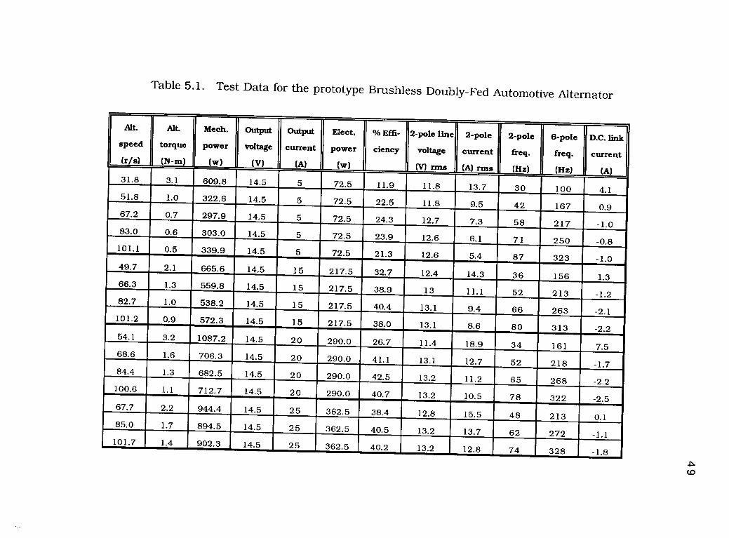
Table 5A. Test Data for the prototype Brushless Doubly-Fed Automotive Alternator
Alt.
speed
(r/s)
Alt.
torque
(N-m)
Mech.
power
(w)
Output
voltage
(V)
Output
current
(A)
Elect.
power
(w)
% Effi-
ciency
2-pole line
voltage
(V) rms
2-pole
current
(A) rms
2-pole
freq.
(Hz)
6-pole
freq.
(Hz)
D.C. link
current
(A)31.8 3.1 609.8 14.5 5 72.5 11.9 11.8 13.7 30 100 4.151.8 1.0 322.6 14.5 5 72.5 22.5 11.8 9.5 42 167 0.967.2 0.7 297.9 14.5 5 72.5 24.3 12.7 7.3 58 217 -1.083.0 0.6 303.0 14.5 5 72.5 23.9 12.6 6.1 71 250 -0.8
101.1 0.5 339.9 14.5 5 72.5 21.3 12.6 5.4 87 323 -1.049.7 2.1 665.6 14.5 15 217.5 32.7 12.4 14.3 36 156 1.366.3 1.3 559.8 14.5 15 217.5 38.9 13 11.1 52 213 -1.282.7 1.0 538.2 14.5 15 217.5 40.4 13.1 9.4 66 263 -2.1
101.2 0.9 572.3 14.5 15 217.5 38.0 13.1 8.6 80 313 -2.254.1 3.2 1087.2 14.5 20 290.0 26.7 11.4 18.9 34 161 7.568.6 1.6 706.3 14.5 20 290.0 41.1 13.1 12.7 52 218 -1.784.4 1.3 682.5 14.5 20 290.0 42.5 13.2 11.2 65 268 -2.2100.6 1.1 712.7 14.5 20 290.0 40.7 13.2 10.5 78 322 -2.567.7 2.2 944.4 14.5 25 362.5 38.4 12.8 15.5 48 213 0.185.0 1.7 894.5 14.5 25 362.5 40.5 13.2 13.7 62 272 -1.1
101.7 1.4 902.3 14.5 25 362.5 40.2 13.2 12.8 74 328 -1.8
50
40 -
30 -
20 -
a4.)
gaz
e
10 . 1 l 1 . l .
2000 3000 4000 5000 6000Alternator Speed (r \min)
7000
Fig. 5.1 BDFAA Performance
5Aa 15A
20 A25 A
50

51
Chapter 6.
Conclusionsand
Recommendations for Future Improvements
6.1 Conclusions
A comparison of Fig. 1.3 and Fig. 5.1 indicates that the proposedalternator system has the potential to compete with the existing caralternator system. Fig. 6.1 shows the performance comparison for 15Aload current.
50
40 -
30 -u
20 -
10-
0 I.I.I.t.2000 3000 4000 5000 6000
Alternator speed (r/min)7000
t3DFAA systemLundell system
Fig. 6.1 Performance Comparison
(Alternator output current 15A, at 14.5V)
52
Unlike in the conventional system, the efficiency curves for theBDFAA system do not vary significantly with speed. This fact is veryimportant as it indicates that the proposed system can maintain goodperformance over a wide speed range. This is essentially achieved bymeans of the EMU.
Efficiency figures for the prototype BDFAA system are lower thanthe conventional system figures. However, this is not the case over theentire speed range. The reason for this is the speed for which themachine is optimized. The conventional system seems to be optimizedfor lower speeds whereas the BDFAA system works better at mediumand higher speeds. The speed range can easily be altered by changingthe engine-to-alternator pulley ratio as required.
The main reason for low efficiency of the prototype system is themachine size. The prototype machine is wound in an inductionmachine frame that was readily available. The machine stack is toolong for the desired output level, resulting in a large magnetizingrequirement, i.e. large control winding currents. In turn, the highcontrol winding currents result in excessive copper losses. Since theinverter supplying the control winding acts as a load on I he system,overall efficiency is reduced.
Also, these high currents the inverter as well as rectifier resultin higher device losses. Low inverter efficiency also brings down theoverall system efficiency.
These problems can be solved by optimizing the machinegeometry for the desired output. With that improvement, the machinecan be expected to support higher load currents than the prototypemachine, which is limited to 25A load current at 14.5V. However, it

53
has been observed that even the conventional alternator system is notcapable of maintaining the output voltage at 14.5V at high loadcurrents.
Other advantages offered by the proposed system are robust andinexpensive structure, brushless operation and no size limitations.
The performance of the two power-electronic units (therectifier and the inverter) is seen to be very important. A high rectifier
efficiency is achieved using Schottky diodes. The inverter efficiency is
low because the device drop, though only 1-2V, is a substantialpercentage of the 14.5V system rating. Therefore, the use of lowvoltage drop devices is very important for both the rectifier andinverter.
The performance of the Voltage Regulator Circuit (VRC) is found
to be quite satisfactory. The circuit is simple and offers an easycalibration method. The Efficiency Maximizer Unit (EMU) carries outthe important task of maintaining maximum efficiency operation over
a wide speed and load range. This circuit is also quite simple. It also
ensures that the system voltage is maintained at 14.5V by generating
appropriate frequency reference signals. A higher precedence is givento the system voltage than to the efficiency maximization, since a lowsystem voltage can adversely affect electrical and electronic loads inthe automobile.
One possible limitation of the BDFAA system could be therequirement of an initial excitation source. The machine, beingsimilar to an induction machine, does not have any remnant field. Inthe case of a conventional system, if the battery is discharged, theremnant field in the rotor can provide self-excitation and can initiate
54
the voltage build-up (using push-start). This is not possible with theBDFAA system. However, in modern vehicles with automatic gears apush-start is not possible. Also, most vehicles with computerizedsystems (i.e. fuel injection) will not start for safety reasons if thebattery voltage is below a certain level. Therefore, the only way to startthe engine is by externally providing the rated voltage, e.g. by means ofa jump-start.
6.2 Recommendations for Future Improvements
A smaller machine (i.e. shorter stack) with more copper areaneeds to be designed. This will improve the regulation and overallefficiency. This will also bring down the device ratings allowing theuse of smaller, cheaper or more efficient devices. Different deviceslike MOSFETs or BJTs (not in Darlington configuration) can be triedfor the inverter once the current levels come down.
For the prototype machine, the only configuration tested wasone with a 6-pole power winding and a 2-pole control winding. Adifferent pole number configuration needs to be investigated, keepingin mind the capability of power generation through the controlwinding.
It is brought out in Section 6.1 that the low system voltage(14.5V) is a cause of the inefficient system operation. The automobilemanufacturers are already planning to go to higher voltage systemssuch as 24V, 36V or even 48V. With the higher voltage systems, the
current ratings would go down for the same output requirements. Thiswill help in achieving better efficiencies. Hence, it is quite clear that
55
systems at higher voltages would be much more efficient and need tobe developed.
The BDFM can generate with d.c. excitation applied to thecontrol winding. This mode has not been explored fully yet for theprototype BDFAA. Though efficiency maximization is not possible withd.c. excitation, under certain conditions, this mode may offer someadvantages with a properly designed machine. For example, even if thebattery is almost discharged, a relatively higher d.c. excitation current
can be supplied for a short duration to initiate the generation. The a.c.excitation current in this low voltage situation would be limited by theinductive reactance of the control winding.
The inverter circuit can be adapted to provide d.c. excitation byturning on any two upper devices and one lower device in theremaining leg, or vice versa. A d.c. modulating signal instead ofsinusoidal modulating waves will allow chopper control to regulate theoutput voltage.
As mentioned in Section 6.1, the machine seems to work betterat higher speeds. Therefore a high pulley ratio can be used to run themachine at higher speeds, even when the engine is idling. Anotheroption is to design a machine for lower speed operation.
The EMU uses engine speed feedback. In the case of theprototype alternator system, it has been observed that the efficiency isoptimized for minimum d.c. link current flowing into the inverter, or,
during regeneration, for maximum d.c. link current flowing out of theinverter. Thus, a current feedback from the d.c. link can also be usedto develop the efficiency maximization unit. This would eliminate the

56
need of external wiring into the alternator casing, since the inverterand the alternator would be in the same enclosure.
The prototype alternator does not provide any systemprotection. Current and voltage limiters are required in the inverter aswell as rectifier circuits to prevent damage.
Finally, system integration is an important task to be considered.The entire semiconductor portion can be put in a single package using
Smart Power technology. For the first level of integration, the rectifierand inverter can be replaced separately with units available in compact
packages. An integrated system would also improve efficiency, sincelosses and voltage drops in leads would be minimized.

57
BIBLIOGRAPHY
[1] Nady Boules, "Performance Requirements for Future Automotive
Electrical Machines", Proceedings: NSF Workshop onElectrical Machines and Drives, 1988. pp 16-21.
[2] R. Wang, N.A. Demerdash, "Extra High Speed Modified
Lundell Parameters and Open/Short Circuit Characteristicsfrom Global 3D-FE Magnetic Field Solutions", IEEE PES WinterMeeting, New York, 1991. Paper 91WM067-9EC.
[3] L.M.C. Mhango, "An Experimental Study of Alternator
Performance Using Two Drive Ratios and a Novel Method of
Speed Boundary Operation", IEEE IAS Annual Meeting,
Seattle, 1990. pp 301-308.
[4] R.D. King, "Combined Electric Starter and Alternator System
Using a Permanent Magnet Synchronous Machine", U.S. PatentNo. 4,862,009.
[5] A.K. Wallace, R. Spee, "Brush less Doubly-Fed Generation System
for Vehicles", US Patent No. 07/560,188.
[6] V.Javadekar, Ravi D.K., R. Spee, A. Wallace, " A Variable-Speed
Brushless Doubly-Fed Automotive Alternator", Conf. Rec.,
EPE,Florence,1991.pp 4-099 4-103.
58
[7] L.J. Hunt, "A New Type of Induction Motor", IEE Journal, 1921.Vol.59, pp 648-677.
[8] F. Creedy, "Some Developments in Multi-Speed Cascade
Induction Motors", IEE Journa1,1921. Vol.59, pp 511-521.
[9] A.R.W. Broadway, B.J. Cook, P.W. Neal, "Brush less Cascade
Alternator", IEE Proc. 1974, Vol.121, pp 1529-1535.
[10] H.K. Lauw, "Characteristics and Analysis of the Brush less Doubly-
Fed Machine", Final Report, US DOE, Contract No. 79-85BP24332, 1989.
[11] R. Spee, A.K. Wallace, H.K. Lauw, "Simulation of Brush less
Doubly-Fed Adjustable Speed Drives", Conf. Rec. IEEE IAS Annual
Meeting,San Diego,1989. pp 738-743.
[12] Ned Mohan, T.M. Undeland, W.P. Robbins, 'Power Electronics:
Converters, Applications and Design'. Wiley,1989.
[13] S.R. Bowes, A. Midoun, "Suboptimal Switching Strategies for
Microprocessor-Controlled PWM Inverter Drives", IEE Proc.
Vo1.132, Pt.B,No.3,May 1985. pp 133-148.
[14] P.N. Enjeti, P.D. Ziogas, J.F. Lindsay, M.H. Rashid, "A New PWM
Speed Control System for High-Performance ac Motor Drives",
59
IEEE Trans. Ind. Electronics,Vol.37,No.2, Apr.1990. pp 143-151.
[15] B.K.Bose, ' Power electronics and AC drives', Prentice-Hall,NJ, 1989.
[16] J.T. Boys, P.G. Handley, "Harmonic Analysis of Space Vector
Modulated PWM Waveforms", IEE Proc. Vol.137,Pt.B, No.4,July1990. pp 197-204.
[17] V.P. Ramamurthi, B. Ramaswami, "A Novel Three-Phase
Reference Sine-Wave Generator for PWM Inverters", IEEETrans. Ind. Electronics, Vol.IE-29,No.3,Aug.1982. pp 235-240.
1181 P. Rochelle, R. Spee, A.K. Wallace, "The Effect of Stator Winding
Configuration on the Performance of BDFM in Adjustable Speed
Drives" Conf. Rec. International Conference for Electrical
Machines, Cambridge, Mass., 1990. pp 54-59.
1191 Ken Layne, 'Automobile Electronics and Basic Electrical
Systems', Wiley, 1990.
[20] Robert G. Irvine, 'Operational Amplifier Characteristics and
Applications', Prentice Hall, 1987.
[21] Benjamin C. Kuo, 'Automatic Control Systems', Prentice Hall ofIndia Pvt. Ltd., 1985.

APPENDICES

60
APPENDIX ITechnical Data for Power Transistors
Technical Data for Power Diodes

61
Technical Data for Power Transistors(from Motorola Bipolar Power Transistor Data-book)
MJ11011 PNPMJ11012 NPN
Darlington Power Transistors
Complementary Silicon
Maximum Ratings
Collector-Emitter Voltage
Collector-Base Voltage
Emitter-Base Voltage
Collector Current
Base Current
Electrical Characteristics
VcE0
VCB
VEB
IC
IB
60Vdc
60Vdc
5Vdc
30Ad c
IAdc
DC Current Gain hFE 1000 min. @ Ic = 20 Adc,
VCE = 5 Vdc.
Collector-Emitter
Saturation Voltage : VCE(sat)
Base-Emitter
Saturation Voltage : VBE(sat)
3 Vdc max. @ Ic = 20 Adc,
IB = 200 mAdc.
3.5 Vdc max. @ Ic = 20 Adc,
IB = 200 mAdc.
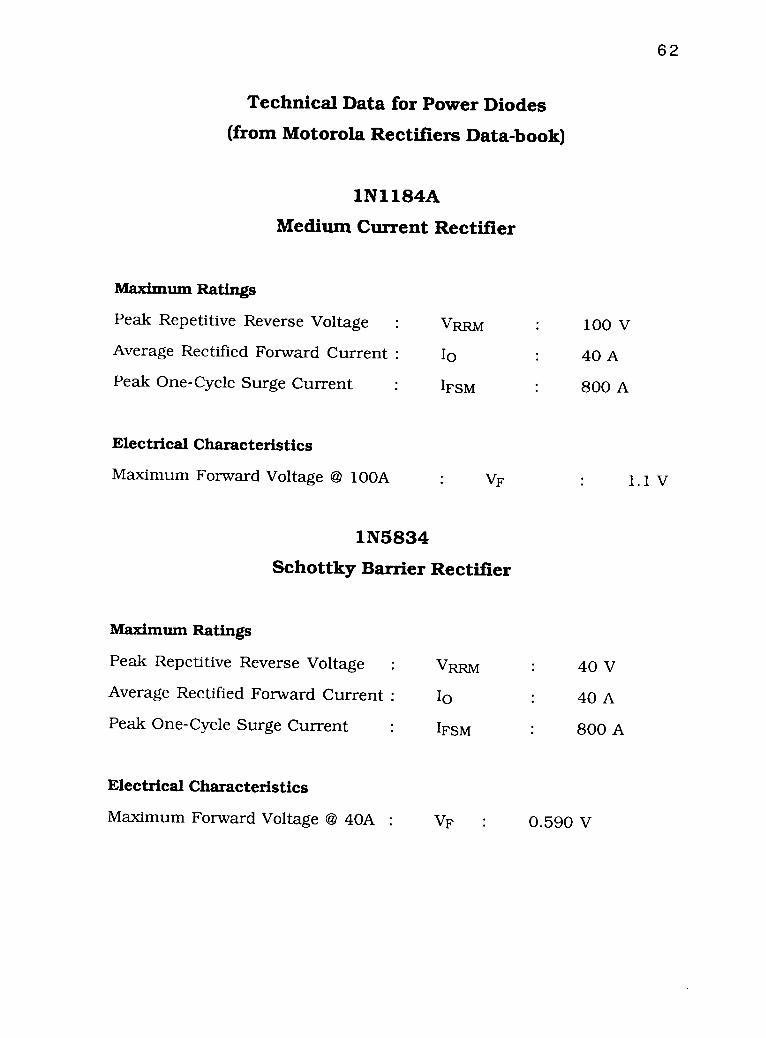
Technical Data for Power Diodes(from Motorola Rectifiers Data-book)
1N1184A
Medium Current Rectifier
Maximum Ratings
Peak Repetitive Reverse Voltage : VRRM 100 V
Average Rectified Forward Current : Io 40 A
Peak One-Cycle Surge Current IFSM 800 A
Electrical Characteristics
Maximum Forward Voltage @ 100A
1N5834
62
VF 1 . 1 V
Schottky Barrier Rectifier
Maximum Ratings
Peak Repetitive Reverse Voltage : VppjAverage Rectified Forward Current : Jo
Peak One-Cycle Surge Current IFSM
Electrical Characteristics
40 V
40 A
800 A
Maximum Forward Voltage © 40A : VF 0.590 V

63
APPENDIX IICircuit Diagrams
Switching Pattern Generator (SPG)
Voltage Regulator Circuit (VRC)
Efficiency Maximization Unit (EMU)

V.
VC! 12K
C){= ;4733k
2N53212
V-
33K
64
20K
NA."1N4735 100K
78KV.
74733K
V-
H-0.01uF
33K
V.
33K
41
V
V V.
18 161
/4
d1v. by6
--
CD4018
Vcf FREQUENCY CONTROL REFERENCE VOLTAGE
TRIANGULAR CARRIER NAVEA.8.0 THREE PHASE SQUARE NAVES
3.3K
i:
1N473S
2K
1N4740
1N4740
CARRIER WAVE AND THREE PHASE SQUARE-WAVE GENERATOR
Fig. II.1 SPG Carrier Wave and Three Phase Square Wave
Generator
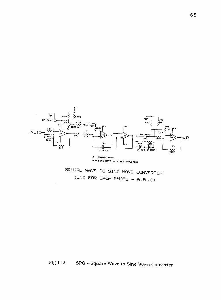
-Vc f
V-
BF 245C
12K
680K
680K
20K560
65
330K
V+2N5322
BF 245C47K 20K
V-33K
0.047uF
A - SQUARE NAVE
1N4735 1 4735
R - SINE NAVE OF FIXED AMPLITUDE
SQUARE WAVE TO SINE WAVE CONVERTER( ONE FOR EACH PHASE A,B,C)
330K
Fig 11.2 SPG Square Wave to Sine Wave Converter
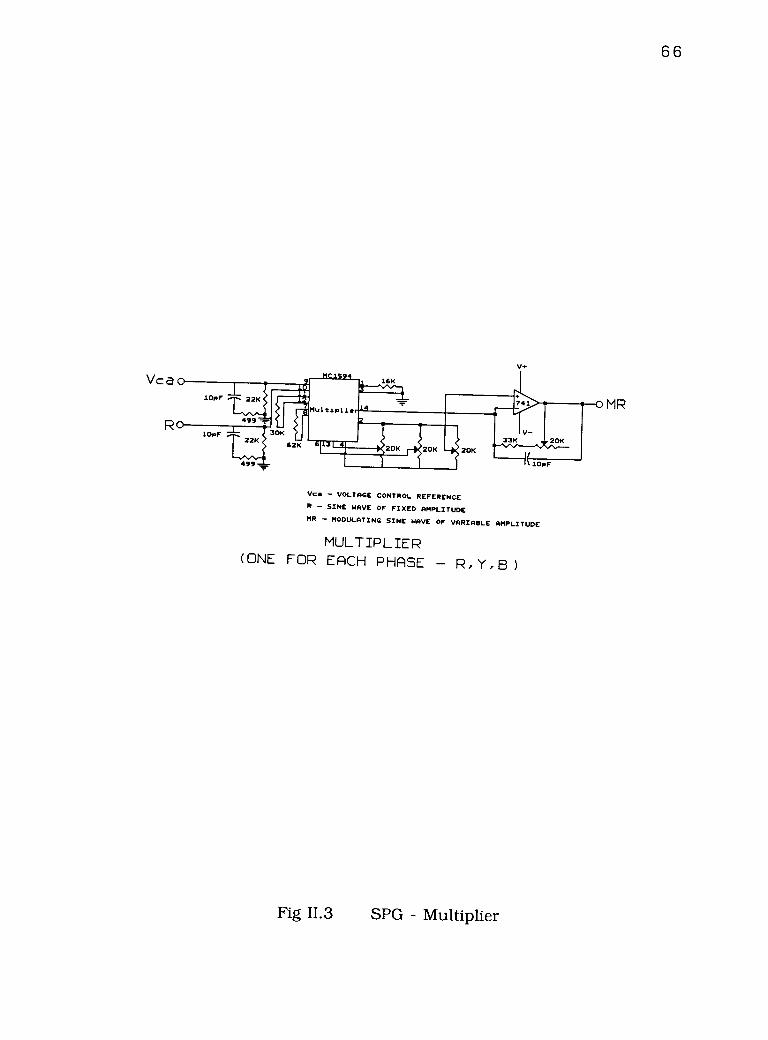
66
.0104611,
Multiplier
MA.I
Vca VOLTAGE CONTROL REFERENCER SINE WAVE OF FIXED AMPLITUDEMR MODULATING SINE WAVE OF VARIABLE AMPLITUDE
MULTIPLIER( ONE FOR EACH PHASE R , Y , )
Fig 11.3 SPG Multiplier
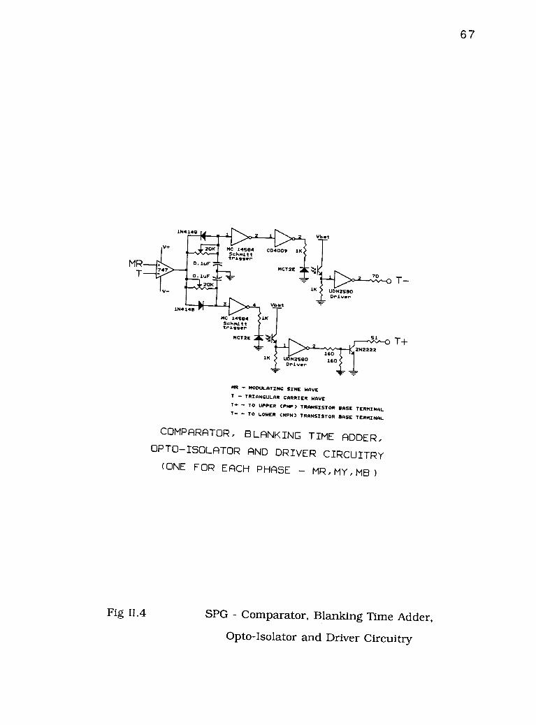
67
MRT
V. 1100P
IMriaMC 14584Schmitttrigger
MCT2E
141111111illi PPP.
20
14
K
Vbet
UDN2580Driver
MC 14584Schmitttrigger
MCT2E
--r1K UON2580 160
Driver
MR - MODULATING SINE NAVE
7 - TRIANGULAR CARRIER WAVE
T. - TO UPPER (PNP) TRANSISTORBASE TERMINAL
T- - TO LONER CNPN)TRANSISTOR BASE TERMINAL
COMPARATOR, B LANKING TIME ADDER,OPTO- ISOLATOR AND DRIVER CIRCUITRY( ONE FOR EACH PHASE MR, MY, MB)
Fig 11.4 SPG Comparator, Blanking Time Adder,
Opto-Isolator and Driver Circuitry
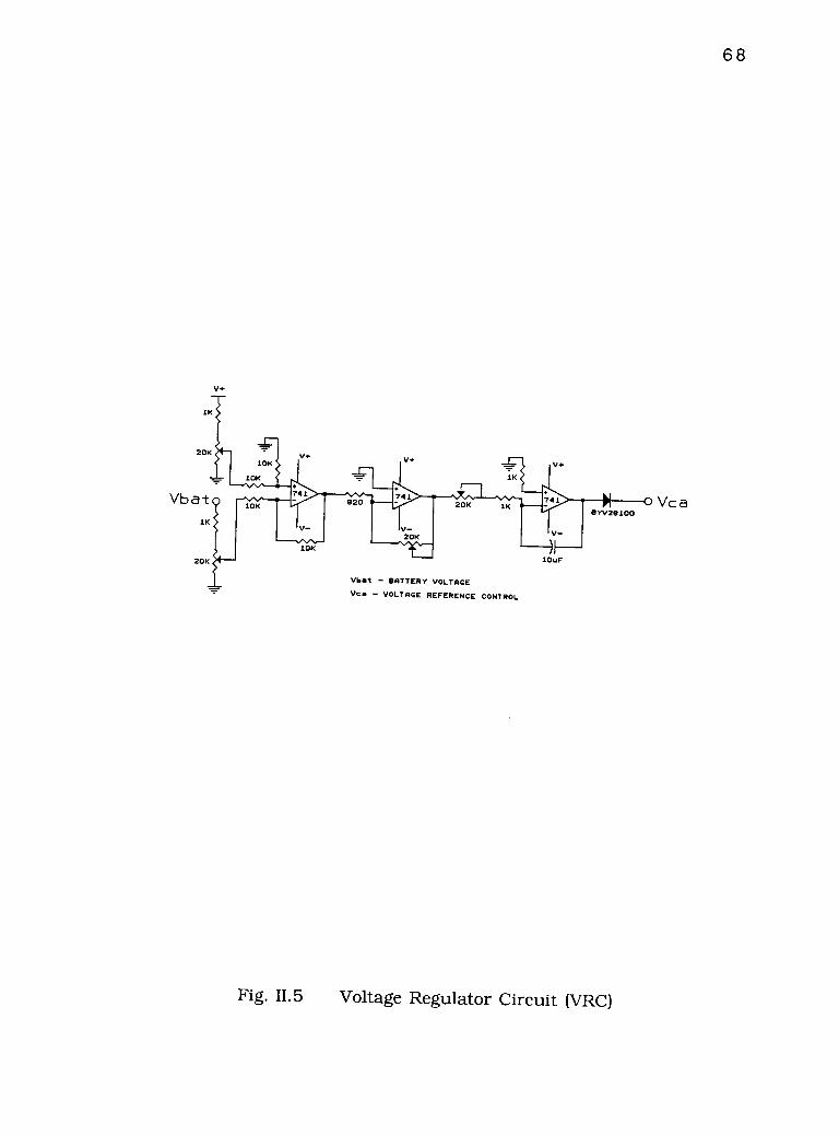
1K
20K
Vb at1K
20K
+
V+ V+ +
20K 1K
V-
----v.v.s.10K
v-20K
Vaat BATTERY VOLTAGEVca VOLTAGE REFERENCE CONTROL
N 0 vcaBYV28100
Fig. 11.5 Voltage Regulator Circuit (VRC)
68
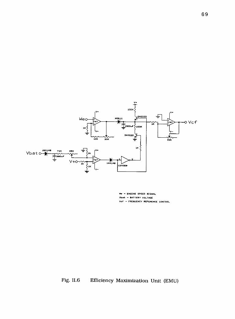
1N4148 715 250Vb a t
TeeouF
v+
W e 0--
K
V.
100K
:11000uF
2N2222
7F
1K
MR811
1DX 20K
2N2222 rI
1N4148
1K C04009
V-
20K
Me ENGINE SPEED SIGNAL
Vbat BATTERY VOLTAGE
Vcf FREQUENCY REFERENCE CONTROL
Fig. 11.6 Efficiency Maximization Unit (EMU)
69