
Degradation in FPGAs: Modelling, Monitoring and Mitigation
201
Degradation in FPGAs Monitoring, Modeling and Mitigation zur Erlangung des akademischen Grades eines Doktors der Ingenieurwissenschaften von der KIT-Fakult¨ at f ¨ ur Informatik des Karlsruher Instituts f ¨ ur Technologie (KIT) genehmigte Dissertation von Abdulazim Amouri aus Aleppo-Syrien Tag der m¨ undlichen Pr ¨ ufung: 23.04.2015 Erster Gutachter: Prof. Dr. Mehdi Baradaran Tahoori, CDNC, Karlsruher Institut f ¨ ur Technologie (KIT), Deutschland Zweiter Gutachter: Prof. Dr. Pascal Benoit, LIRMM, Universit¨ at Montpellier 2, Frankreich
-
Upload
khangminh22 -
Category
Documents
-
view
3 -
download
0
Transcript of Degradation in FPGAs: Modelling, Monitoring and Mitigation

Degradation in FPGAsMonitoring, Modeling and Mitigation
zur Erlangung des akademischen Grades eines
Doktors der Ingenieurwissenschaften
von der KIT-Fakultat fur Informatikdes Karlsruher Instituts fur Technologie (KIT)
genehmigteDissertation
von
Abdulazim Amouriaus Aleppo-Syrien
Tag der mundlichen Prufung: 23.04.2015
Erster Gutachter: Prof. Dr. Mehdi Baradaran Tahoori,CDNC, Karlsruher Institut fur Technologie (KIT), Deutschland
Zweiter Gutachter: Prof. Dr. Pascal Benoit,LIRMM, Universitat Montpellier 2, Frankreich

This document is licensed under the Creative Commons Attribution – Share Alike 3.0 DE License (CC BY-SA 3.0 DE): http://creativecommons.org/licenses/by-sa/3.0/de/

Ich versichere hiermit wahrheitsgemaß, die Dissertation bis auf die dort angegebe-nen Hilfen selbststandig angefertigt, alle benutzten Hilfsmittel vollstandig und genauangegeben und als kenntlich gemacht zu haben, was aus Arbeiten anderer und eigenenVeroffentlichungen unverandert oder mit Anderungen entnommen wurde.
Karlsruhe, 05.03.2015
Abdulazim Amouri


Dedication
To whom, who taught me my first letters...To whom, who planted in me the love of learning and discovering...To whom, who opened my eyes to the unknowns of this world and guided me to discover...To whom, God ordered me to acknowledge and respect them...To my parents ... I love you too much
***
To whom, who change my life...To whom, who taught me the patience...To whom, who loved me, helped me, encouraged me and was always beside me...To my wife ... I love you
***
To whom, who bring the happiness into my world...To whom, who make me feel the responsibility...To whom, who make me look into the future...To my children ... I love you
***
I dedicate this work to all of my family members and to the people of Syria, who arestill suffering the war for 4 years.
i


Acknowledgment
My cordial gratitude is presented to my advisor Prof. Dr. Mehdi Tahoori, this great personfrom whom I learned a lot, who guided me through my research and give me the flexibilityto try and discover, who unleashed my creativity to deal with the most challenging tasks.This great person, who kept a high level of patience in spite of all my nonsense ... I’m verythankful.
I’m also grateful to my co-advisor Prof. Dr. Pascal Benoit and his assistant Dr. FlorentBruguier for the nice and fruitful collaboration and for their warm welcome during my visitto Montpellier. Furthermore, my special thanks to Prof. Dr. Jorg Henkel and his assistantsMr. Hussam Amrouch and Dr. Thomas Ebi for the fruitful collaboration.
I would like to present my heartfelt thanks to all of my colleagues and project partnersat the Chair of Dependable Nano Computing (CDNC) for the nice period I spent betweenthem and the family atmosphere they have created at our chair and also for all their valuablefeedback and discussions. In particular I want to thank (in alphabetical order): MatthiasBeste, Liang Chen, Mojtaba Ebrahimi, Farshad Firouzi, Saman Kiamehr, Fabian Oboril andParthasarathy Murali Baskar Rao. I also want to thank Jochen Hepp, whom I supervisedin the scope of his Master thesis for his nice work. Furthermore, my special thanks to mycolleagues Fabian Oboril, Artjom Grudnitsky and Gabriel Cadilha Marques for correctingmy German translation of the abstract of this dissertation. Finally, my thanks to all thesecretaries and technicians at our institute in particular to Mrs. Iris Schrder-Piepka, Mrs.Renate Murr-Grobe and Mr. Martin Buchty for all of their efforts in providing a goodworking environment.
iii


List of own publications included in this dissertation
Book Chapters
[B.1] A. Amouri, M. Tahoori, ”Lifetime Reliability Sensing in ModernFPGAs”, In P. Athanas, D. Pnevmatikatos, N. Sklavos, editors, ”Em-bedded Systems Design with FPGAs”, Springer, ISBN 978-1-4614-1361-5, 2013.
Conference Papers
[C.1] A. Amouri, F. Bruguier, S. Kiamehr, P. Benoit, L. Torres andM. Tahoori, ”Aging Effects in FPGAs: an Experimental Analy-sis”, Proceedings of the 24th International Conference on Field Pro-grammable Logic and Applications (FPL), IEEE, 2014, Munich,Germany.
[C.2] A. Amouri, J. Hepp, and M. Tahoori, ”Self-Heating Thermal-AwareTesting of FPGAs”, Proceedings of the 32nd IEEE VLSI Test Sym-posium (VTS), pages 1-6, 2014, Napa, California, USA.
[C.3] A. Amouri and M. Tahoori, ”Degradation in FPGAs: Monitor-ing, Modeling and Mitigation (PHD forum paper: Thesis broadoverview)”, Proceedings of the 23rd International Conference onField Programmable Logic and Applications (FPL), pages 12, IEEE,2013, Porto, Portugal.
[C.4] P.M.B. Rao, A. Amouri, S. Kiamehr, and M. Tahoori, ”AlteringLUT Configuration for Wear-out Mitigation of FPGA-Mapped De-signs”, Proceedings of the 23rd International Conference on FieldProgrammable Logic and Applications (FPL), pages 18, IEEE, 2013,Porto, Portugal.
[C.5] A. Amouri, H. Amrouch, T. Ebi, J. Henkel and M. Tahoori, ”Accu-rate Thermal-Profile Estimation and Validation for FPGA-MappedCircuits”, Proceedings of the 21st IEEE International Symposium onField-Programmable Custom Computing Machines (FCCM), pages57-60, 2013, Seattle, Washington, USA.
v

[C.6] A. Amouri, S. Kiamehr and M. Tahoori, ”Investigation of Aging Ef-fects in Different Implementations and Structures of ProgrammableRouting Resources of FPGAs”, Proceedings of the 2012 InternationalConference of Field-Programmable Technology (FPT), pages 215-219, IEEE, 2012, Seoul, South Korea.
[C.7] A. Amouri and M. Tahoori, ”High-Level Aging Estimation ForFPGA-Mapped Designs”, Proceedings of the 22nd InternationalConference on Field Programmable Logic and Applications (FPL),pages 284-291, IEEE, 2012, Oslo, Norway.
[C.8] S. Kiamehr, A. Amouri and M. Tahoori, ”Investigation of NBTI andPBTI Induced Aging in Different LUT Implementations”, Proceed-ings of the 2011 International Conference of Field-ProgrammableTechnology (FPT), pages 1-8, IEEE, 2011, New Delhi, India
[C.9] A. Amouri and M. Tahoori, ”A Low-Cost Sensor for Aging and LateTransitions Detection in Modern FPGAs”, Proceedings of the 21stInternational Conference on Field Programmable Logic and Appli-cations (FPL), pages 329-335, IEEE, 2011, Chania, Greece.
Journal Papers
[J.1] A. Amouri, J. Hepp, and M. Tahoori, ”Built-in Self-Heating Ther-mal Testing of FPGAs”, Transactions on Computer-Aided Design ofIntegrated Circuits and Systems (TCAD) (Accepted for publication,November 2015)
vi

Abstract
The quest for high performance circuits with low power consumption, large scale inte-gration and low cost, is the main reason behind the continuous shrinking of transistors’dimensions at nano-scale. This shrinking has already reached critical limits posing vari-ous manufacturing and reliability challenges to Very Large Scale Integration (VLSI) chips.Nowadays, the transistor degradation mechanisms (a.k.a. transistor aging) and the thermal-related issues (heat dissipation, hot spots, etc.) are among the most important challengesthat affect the reliability of the VLSI chips.
Field Programmable Gate Arrays (FPGAs) are general purpose reconfigurable chips pro-viding many unique features and capabilities over Application-Specific Integrated Circuits(ASICs). The FPGA design philosophy as compared to that of ASIC is based on both theconcept of rapid development (faster time to market) and the in-field programming concept.Hence, unlike ASICs, the circuit can be deployed directly onto the FPGA without the needto worry about the manufacturing process and the FPGA chips can be easily reconfiguredin the field as desired to accomplish different functions. For these reasons, FPGAs are usedin a wide range of applications, where faster time to market and/or in-field reconfigurationsare required. For many of these applications the reliability is very critical and comes asa first priority. State-of-the-art FPGAs, pushed by the ever-increasing demands on higherperformance and lower power, use the latest advancements in VLSI technology, and thusthey share most of the reliability challenges associated with nano-scale technology nodes.Therefore, to guarantee the correct functionality during the lifetime of FPGA-mapped sys-tems in the field, proper techniques at various levels should be devised.
Transistor aging, as an important reliability threat at nano-scale technologies, causeschanges in the transistor characteristics, which slow down the switching speed of the tran-sistor over time and in turn leads to timing failures in the chip. This issue has been ad-dressed in literature mainly for ASICs and at the device-level alone. In order to be able tofortify against the aging effects in FPGA, it is necessary to estimate the amount of degrada-tion for the whole FPGA-mapped circuit early at design phase. However, it is infeasible toestimate the aging for a complete design using directly the models and techniques proposedat device-level. This is because of the simulation overhead at device-level and its complex-ity. That is why only experimental methods have been followed in literature to investigatethe aging of FPGA. Based on that, there is a need for fast and accurate aging estimationat higher level, even if it is inherently less accurate than the device-level correspondent. Infact, to properly deal with aging in FPGAs, it requires monitoring, modeling and mitiga-tion at device and architecture levels and this must be integrated in the tool-chain used fordeveloping the FPGA designs at user side.
This dissertation targets the transistor aging degradation as well as the associated ther-mal challenges in FPGAs (since there is an exponential relation between aging and chiptemperature). The main objectives are to perform experimentation, analysis and device-
vii

Abstract
level model abstraction for modeling the degradation in FPGAs, then to monitor the FPGAto keep track of aging rates and ultimately to propose an aging-aware FPGA design flowto mitigate the aging. The contributions presented in this dissertation can be divided intothree main parts: modeling, monitoring and mitigation. For modeling the aging effects inFPGA, device-level investigations are carried out on fundamental FPGA building blocks(look-up tables and routing switch matrices) to understand the effects of aging on FPGAarchitecture. Furthermore, FPGA stress experiments with controlled stress conditions aremade to measure the extent of degradation and the role of different parameters in the FPGAdegradation. Additionally, a method for estimating the thermal-profile of FPGA-mappeddesigns is proposed, which is verified by real thermal measurements. Based on the resultsof these real experiments, an aging modeling framework for FPGA is proposed by combin-ing both the accurate device-level models and the implicit high-level details in the FPGAdesign tools. Using this framework, several mitigation strategies are proposed to reduce theeffect of aging on the total lifetime of the FPGA-mapped design. These strategies are basedon an aging-aware logic mapping that targets directly the look-up tables of the FPGA.
As the effects of aging appear on a long time-scale and also they are process- and usage-dependent, a tracking of these effects is important to maintain the correct functionality ofthe mapped design throughout the FPGA lifetime. For monitoring the aging effects in FP-GAs, logic-based sensors exploiting the existing programmable FPGA resources, are pre-sented to monitor the effect of aging on the most critical paths of FPGA-mapped designs.Additionally, different techniques are proposed for thermal-aware functional testing of theFPGA using self-heating modules that are built on top of FPGA programmable resources.
The results of these contributions have been integrated in an aging-analysis-and-mitigation toolset, which takes as input the information available to the FPGA-users abouttheir designs in order to estimate the total expected lifetime and performs various modifi-cations to meet the lifetime reliability requirements. These results can be even integrated inthe FPGA tools provided by the manufacturer with more accurate models for aging-awareplacement and routing. Additionally the investigation results can be used to build an aging-aware FPGA chip, in which the FPGA building blocks are designed with aging effects inmind from the transistor-level upwards to the whole FPGA.
viii

Zusammenfassung
Die Suche nach hochleistungsfahigen Schaltungen mit niedrigem Stromverbrauch, ho-her Integrationsdichte und geringen Kosten, ist der Hauptgrund fur das kontinuierlicheSchrumpfen der Transistordimensionen bis in den Nanometer-Bereich. Das Schrumpfenhat jedoch bereits kritische Grenzen erreicht, die verschiedene Herstellung- und Zu-verlassigkeitsherausforderungen an Very Large Scale Integration (VLSI)-Chips stellen.Heutzutage gehoren die Transistorabbaumechanismen (auch bekannt als Transistor-alterung) und die thermischen Probleme (Warmeableitung, Hot Spots, etc.) zu den wichtig-sten Herausforderungen, die die Zuverlassigkeit der VLSI-Chips beeinflussen.
Im-Feld programmierbare Logik-Gatter-Anordnungen (FPGAs) sind rekonfigurierbareChips fur allgemeine Anwendungen, die viele einzigartige Funktionen und Fahigkeitengegenuber anwendungsspezifische integrierte Schaltungen (ASICs) besizen. Die FPGA-Entwurfsphilosophie basiert dabei, im Vergleich zu jener der ASICs, auf zwei wesentlichenKonzepten: Schnelle Prototypen-Entwicklung (und damit schnellere Markt-einfuhrung)und der Rekonfigurierbarkeit wahrend der Nutzung. Deshalb konnen, anders als inASICs, Schaltkreise auf einem FPGA implementiert werden, ohne sich um den Herstel-lungsprozess zu kummern. Die FPGA-Chips konnen im Betrieb nach Wunsch neu kon-figuriert werden, um verschiedene Funktionen auszufuhren. Aus diesen Grunden werdenFPGAs in einer Vielzahl von Anwendungen eingesetzt, in denen eine schnellere Markte-infuhrung und/oder im Feld Neukonfigurationen erforderlich sind. Fur viele dieser Anwen-dungen ist die Zuverlassigkeit sehr kritisch und hat daher erste Prioritat. Moderne FPGAsnutzen die neuesten Fortschritte der VLSI-Technologie, durch die standig steigende An-forderungen an die hohere Leistung und geringerem Stromverbrauch, und teilen sich damitdie meisten Zuverlassigkeitsherausforderungen, die mit Nanometer-technologien verbun-den sind. Deshalb mussen sachgemaße Techniken auf verschiedenen Abstraktionsebenenentwickelt werden, um die korrekte Funktion im Betrieb der FPGA-basierten Systeme zugewahrleisten.
Transistoralterung, als eine wichtige Zuverlassigkeitsherausforderung bei Struk-turgrossen im Nanobereich, fuhrt zu Veranderungen in den Transistoreigenschaften, diedie Schaltgeschwindigkeit der Transistorn mit der Zeit verlangsamen und damit wiederumzu Chipausfallen fuhren konnen. Dieses Problem wurde in der Literatur vor allem furASICs und auf Transistoren-Ebene angegangen. Um in der Lage zu sein die Alterungsef-fekte in FPGAs verlangsamen zu konnen, ist es notwendig die Alterung fruh in der Ent-wurfsphase abzuschatzen. Es ist jedoch unmoglich, die Alterung fur einen komplettenEntwurf direkt mit Modellen und Techniken auf Transistor-Ebene abzuschatzen, aufgrunddes Simulationsaufwands auf Transistor-Ebene und der verbundenen Komplexitat. Deshalbsind nur experimentelle Methoden in der Literatur verfolgt worden, um die Alterung vonFPGAs zu untersuchen. Somit gibt es einen großen Bedarf fur schnelle und genaue Al-terungsschatzungen auf hoheren Abstraktionsebenen, auch wenn diese weniger exakt sind,
ix

Zusammenfassung
als die Transistor-Ebene-Abschatzung. Fur den richtigen Umgang mit der Alterung in FP-GAs werden Uberwachung, Modellierung und Minderung der Alterung auf Transistor- undArchitekturebenen benotigt. Daruber hinaus muss all dies in die Werkzeugkette, die fur dieEntwicklung der FPGA-Designs auf Anwenderseite verwendet wird, integriert werden.
Diese Dissertation befasst sich mit der Alterung von FPGAs, sowie den damit verbun-denen thermischen Probleme in FPGAs (da es eine exponentielle Beziehung zwischen Al-terung und Chiptemperatur gibt). Die in dieser Arbeit vorgestellten Beitrage lassen sichin drei Hauptteile gliedern: Modellierung, Uberwachung und Minderung. Fur die Model-lierung der Alterungseffekte in FPGAs werden Untersuchungen auf Transistor-Ebene furdie Grund-FPGA-Bausteine durchgefuhrt (Look-up Tables und Routing Schaltmatrizen),um die Auswirkungen der Alterung auf die FPGA-Architektur zu verstehen. Weiterhinwerden FPGA-Stressexperimente mit kontrollierten Belastungsbedingungen durchgefuhrt,um das Ausmaß der Alterung und den Einfluss der verschiedenen Parameter auf dieAlterung von FPGAs zu messen. Zusatzlich wird ein Verfahren zum Abschatzen desWarmeprofils vorgeschlagen, dass durch reale thermische Messungen verifiziert/validiertwird. Basierend auf den Ergebnissen dieser realen Experimente wird eine Platform zur Al-terungsmodellierung fur FPGAs vorgeschlagen. Mit dieser Platform werden verschiedeneAbwehrstrategien entwickelt, die die Auswirkungen der Alterung auf die Gesamtlaufzeitdes FPGAs reduzieren. Diese Strategien basieren auf einer alterungsbewusste Logik-Zuordnung, und arbeiten direkt auf den Look-up Tables des FPGAs.
Da die Auswirkungen der Alterungseffekte uber einen langen Zeitraum erkennbar wer-den und sie auch Prozess- und Nutzungsabhangig sind, ist eine Uberwachung dieser Effektewichtig, um die richtige Funktionalitat uber die gesamte FPGA Lebensdauer zu halten. ZurUberwachung der Alterungseffekte in FPGAs werden Logik-Sensoren, die die bestehendenprogrammierbaren FPGA-Ressourcen nutzen, entwickelt, um den Effekt der Alterung aufden kritischen Pfaden der FPGA-basierten Entwurfen zu uberwachen. Zusatzlich werdenverschiedene Techniken fur die thermische sensitive Funktionalitatsprufung des FPGAsdurch sich selbst aufheizende Module vorgeschlagen, die auf den Resourcen des FPGAsaufgebaut sind.
Die Ergebnisse dieser Beitrage wurden in ein Toolset fur Alterungsanalyse und Min-derung integriert, dass als Eingabe die Information, die dem FPGA-Nutzer uber seineEntwurfe zur Verfugung stehen, nimmt, um die gesamte erwartete Lebensdauer zu schatzenund dann verschiedene Modifikationen durchfuhrt, um die Anforderungen bzgl. der Zu-verlassigkeit uber die gesamten Lebensdauer zu erfullen. Diese Ergebnisse konnen auchmit den FPGA-Tools von kommerziellen Herstellern mit genaueren Alterungsmodellen furalterungsbewusste Platzierung und Verdrahtung benutzt werden. Zusatzlich konnen dieUntersuchungsergebnisse verwendet werden, um einen alterungsbewusstes FPGA-Chip zubauen, in dem die FPGA-Bausteine mit Berucksichtigung von Alterungseffekten von derTransistor-Ebene aufwarts entwickelt werden.
x

Contents
Abstract vii
Zusammenfassung ix
1. Introduction 11.1. FPGAs and technology scaling . . . . . . . . . . . . . . . . . . . . . . . . 11.2. Degradation and reliability challenges of FPGAs . . . . . . . . . . . . . . 31.3. Dissertation focus and goals . . . . . . . . . . . . . . . . . . . . . . . . . 5
1.3.1. Investigation and Modeling . . . . . . . . . . . . . . . . . . . . . . 51.3.2. Monitoring . . . . . . . . . . . . . . . . . . . . . . . . . . . . . . 61.3.3. Mitigation . . . . . . . . . . . . . . . . . . . . . . . . . . . . . . . 6
1.4. Dissertation outline . . . . . . . . . . . . . . . . . . . . . . . . . . . . . . 8
2. Background 92.1. FPGA architecture . . . . . . . . . . . . . . . . . . . . . . . . . . . . . . 9
2.1.1. Configurable Logic Block (CLB) . . . . . . . . . . . . . . . . . . 102.1.2. Switch Matrix . . . . . . . . . . . . . . . . . . . . . . . . . . . . 102.1.3. Other components . . . . . . . . . . . . . . . . . . . . . . . . . . 12
2.2. Circuit aging . . . . . . . . . . . . . . . . . . . . . . . . . . . . . . . . . 132.2.1. Transistor aging . . . . . . . . . . . . . . . . . . . . . . . . . . . . 132.2.2. Interconnects aging . . . . . . . . . . . . . . . . . . . . . . . . . . 21
I. Investigation and Modeling 23
3. Investigating The Degradation of LUTs 253.1. Introduction . . . . . . . . . . . . . . . . . . . . . . . . . . . . . . . . . . 253.2. Related Work . . . . . . . . . . . . . . . . . . . . . . . . . . . . . . . . . 263.3. LUT structures . . . . . . . . . . . . . . . . . . . . . . . . . . . . . . . . 26
3.3.1. Two-input LUT structures . . . . . . . . . . . . . . . . . . . . . . 263.3.2. Four-input LUT structures . . . . . . . . . . . . . . . . . . . . . . 30
3.4. Evaluation methodology . . . . . . . . . . . . . . . . . . . . . . . . . . . 303.4.1. Two-input LUTs . . . . . . . . . . . . . . . . . . . . . . . . . . . 313.4.2. Four-input LUTs . . . . . . . . . . . . . . . . . . . . . . . . . . . 32
3.5. Experimental results and analysis . . . . . . . . . . . . . . . . . . . . . . . 353.5.1. Two-input LUTs results . . . . . . . . . . . . . . . . . . . . . . . 363.5.2. Four-input LUTs results . . . . . . . . . . . . . . . . . . . . . . . 41
3.6. Summary . . . . . . . . . . . . . . . . . . . . . . . . . . . . . . . . . . . 44
xi

Contents
4. Investigating The Degradation of Programmable Routing Resources 474.1. Introduction . . . . . . . . . . . . . . . . . . . . . . . . . . . . . . . . . . 474.2. Programmable Routing Switches in FPGAs . . . . . . . . . . . . . . . . . 47
4.2.1. Pass Transistor with keeper (PT-keeper) . . . . . . . . . . . . . . . 484.2.2. Tri-State buffer (TS-buffer) . . . . . . . . . . . . . . . . . . . . . . 494.2.3. Transmission Gate (TG) . . . . . . . . . . . . . . . . . . . . . . . 494.2.4. Multiplexer (MUX) . . . . . . . . . . . . . . . . . . . . . . . . . . 50
4.3. Evaluation Methodology . . . . . . . . . . . . . . . . . . . . . . . . . . . 504.3.1. Circuit-level details and assumptions . . . . . . . . . . . . . . . . 504.3.2. NBTI/PBTI effect analysis . . . . . . . . . . . . . . . . . . . . . . 504.3.3. Delay measurements . . . . . . . . . . . . . . . . . . . . . . . . . 514.3.4. Load analysis . . . . . . . . . . . . . . . . . . . . . . . . . . . . . 51
4.4. Experimental Results . . . . . . . . . . . . . . . . . . . . . . . . . . . . . 524.4.1. Effect of NCS . . . . . . . . . . . . . . . . . . . . . . . . . . . . . 524.4.2. Effect of WL . . . . . . . . . . . . . . . . . . . . . . . . . . . . . 544.4.3. Combined influence of both WL and NCS . . . . . . . . . . . . . . 544.4.4. Effect of Fan-out . . . . . . . . . . . . . . . . . . . . . . . . . . . 544.4.5. Effect of Vdd . . . . . . . . . . . . . . . . . . . . . . . . . . . . . 54
4.5. Summary . . . . . . . . . . . . . . . . . . . . . . . . . . . . . . . . . . . 58
5. Experimental Analysis of Aging Effects 595.1. Introduction . . . . . . . . . . . . . . . . . . . . . . . . . . . . . . . . . . 595.2. Related work . . . . . . . . . . . . . . . . . . . . . . . . . . . . . . . . . 605.3. Sensors design and implementation . . . . . . . . . . . . . . . . . . . . . . 60
5.3.1. Sensors design . . . . . . . . . . . . . . . . . . . . . . . . . . . . 605.3.2. Implementation . . . . . . . . . . . . . . . . . . . . . . . . . . . . 62
5.4. Experimental setup and schedule . . . . . . . . . . . . . . . . . . . . . . . 645.4.1. Setup . . . . . . . . . . . . . . . . . . . . . . . . . . . . . . . . . 655.4.2. Schedule . . . . . . . . . . . . . . . . . . . . . . . . . . . . . . . 65
5.5. Experimental results and analysis . . . . . . . . . . . . . . . . . . . . . . . 665.5.1. Results . . . . . . . . . . . . . . . . . . . . . . . . . . . . . . . . 665.5.2. Analysis . . . . . . . . . . . . . . . . . . . . . . . . . . . . . . . 69
5.6. Summary . . . . . . . . . . . . . . . . . . . . . . . . . . . . . . . . . . . 75
6. Thermal-Profile Estimation of FPGA-Mapped Designs 776.1. Introduction . . . . . . . . . . . . . . . . . . . . . . . . . . . . . . . . . . 776.2. Related work . . . . . . . . . . . . . . . . . . . . . . . . . . . . . . . . . 786.3. Motivation . . . . . . . . . . . . . . . . . . . . . . . . . . . . . . . . . . . 79
6.3.1. Leakage-Temperature Relation . . . . . . . . . . . . . . . . . . . . 796.3.2. FPGA Leakage Power . . . . . . . . . . . . . . . . . . . . . . . . 80
6.4. The Proposed Approach . . . . . . . . . . . . . . . . . . . . . . . . . . . 816.4.1. Leakage Power Redistribution . . . . . . . . . . . . . . . . . . . . 816.4.2. Temperature-Leakage Loop Estimation . . . . . . . . . . . . . . . 81
xii

Contents
6.5. FPGA Thermal Estimation Flow . . . . . . . . . . . . . . . . . . . . . . . 836.5.1. Floorplan Creation . . . . . . . . . . . . . . . . . . . . . . . . . . 836.5.2. Power Trace Generation . . . . . . . . . . . . . . . . . . . . . . . 846.5.3. Thermal Profile Estimation For Dynamically Changing Circuits . . 85
6.6. Experimental Setup . . . . . . . . . . . . . . . . . . . . . . . . . . . . . . 876.6.1. Thermal Camera Usage . . . . . . . . . . . . . . . . . . . . . . . . 876.6.2. Model Calibration . . . . . . . . . . . . . . . . . . . . . . . . . . 87
6.7. Experimental Results . . . . . . . . . . . . . . . . . . . . . . . . . . . . . 876.8. Summary . . . . . . . . . . . . . . . . . . . . . . . . . . . . . . . . . . . 88
7. High-level Aging Estimation 937.1. Introduction . . . . . . . . . . . . . . . . . . . . . . . . . . . . . . . . . . 937.2. Related Work . . . . . . . . . . . . . . . . . . . . . . . . . . . . . . . . . 947.3. Methodology . . . . . . . . . . . . . . . . . . . . . . . . . . . . . . . . . 94
7.3.1. Aging model abstraction . . . . . . . . . . . . . . . . . . . . . . . 957.3.2. Information gathering . . . . . . . . . . . . . . . . . . . . . . . . 977.3.3. Aging estimation . . . . . . . . . . . . . . . . . . . . . . . . . . . 100
7.4. Experimental results . . . . . . . . . . . . . . . . . . . . . . . . . . . . . 1017.4.1. Validation of the abstracted aging model . . . . . . . . . . . . . . . 1017.4.2. Case study: influence of mapping and optimization algorithms . . . 101
7.5. Summary . . . . . . . . . . . . . . . . . . . . . . . . . . . . . . . . . . . 106
II. Monitoring 107
8. Aging Monitoring in FPGA-Mapped Designs 1098.1. Introduction . . . . . . . . . . . . . . . . . . . . . . . . . . . . . . . . . . 1098.2. Related Work . . . . . . . . . . . . . . . . . . . . . . . . . . . . . . . . . 1098.3. Aging Sensor: Main Idea . . . . . . . . . . . . . . . . . . . . . . . . . . . 111
8.3.1. Critical path and aging . . . . . . . . . . . . . . . . . . . . . . . . 1118.3.2. The proposed sensor . . . . . . . . . . . . . . . . . . . . . . . . . 1118.3.3. Sensor sensitivity analysis . . . . . . . . . . . . . . . . . . . . . . 114
8.4. Sensor Mapping . . . . . . . . . . . . . . . . . . . . . . . . . . . . . . . . 1168.4.1. Mapping to logic slices . . . . . . . . . . . . . . . . . . . . . . . . 1178.4.2. Detection window generation . . . . . . . . . . . . . . . . . . . . 1188.4.3. Glitches in FPGA . . . . . . . . . . . . . . . . . . . . . . . . . . . 1188.4.4. Aging sensor placement and calibration . . . . . . . . . . . . . . . 119
8.5. Experimental Results . . . . . . . . . . . . . . . . . . . . . . . . . . . . . 1218.5.1. FPGA design tool experiments (simulation results) . . . . . . . . . 1218.5.2. FPGA board experiment (emulation results) . . . . . . . . . . . . . 122
8.6. Summary . . . . . . . . . . . . . . . . . . . . . . . . . . . . . . . . . . . 125
9. Self-Heating Thermal-Aware Testing of FPGAs 1279.1. Introduction . . . . . . . . . . . . . . . . . . . . . . . . . . . . . . . . . . 127
xiii

Contents
9.2. Related Work . . . . . . . . . . . . . . . . . . . . . . . . . . . . . . . . . 1289.3. FPGA Self-Heating . . . . . . . . . . . . . . . . . . . . . . . . . . . . . . 129
9.3.1. The concept of self-heating . . . . . . . . . . . . . . . . . . . . . . 1299.3.2. Self-Heating Elements (SHEs) . . . . . . . . . . . . . . . . . . . . 1299.3.3. Chain of SHEs: easier controlling . . . . . . . . . . . . . . . . . . 131
9.4. Thermal profile for testing . . . . . . . . . . . . . . . . . . . . . . . . . . 1339.4.1. Distribution of SHEs . . . . . . . . . . . . . . . . . . . . . . . . . 1339.4.2. Calibration process . . . . . . . . . . . . . . . . . . . . . . . . . . 1349.4.3. Integration of SHEs . . . . . . . . . . . . . . . . . . . . . . . . . . 1359.4.4. Other thermal constraints . . . . . . . . . . . . . . . . . . . . . . . 136
9.5. Self-heating application-independent BIST . . . . . . . . . . . . . . . . . 1369.5.1. Sequential method . . . . . . . . . . . . . . . . . . . . . . . . . . 1369.5.2. Concurrent method . . . . . . . . . . . . . . . . . . . . . . . . . . 1379.5.3. Case study BIST implementation . . . . . . . . . . . . . . . . . . 137
9.6. Self-heating application-dependent testing . . . . . . . . . . . . . . . . . . 1419.6.1. Application-dependent testing . . . . . . . . . . . . . . . . . . . . 1419.6.2. SHEs integration methods . . . . . . . . . . . . . . . . . . . . . . 142
9.7. Experimental Results . . . . . . . . . . . . . . . . . . . . . . . . . . . . . 1449.7.1. Self-heating application-independent BIST . . . . . . . . . . . . . 1449.7.2. Self-heating application-dependent test . . . . . . . . . . . . . . . 147
9.8. Summary . . . . . . . . . . . . . . . . . . . . . . . . . . . . . . . . . . . 150
III. Mitigation 151
10.Aging Mitigation in LUTs 15310.1. Introduction . . . . . . . . . . . . . . . . . . . . . . . . . . . . . . . . . . 15310.2. Related Work . . . . . . . . . . . . . . . . . . . . . . . . . . . . . . . . . 15310.3. Motivation . . . . . . . . . . . . . . . . . . . . . . . . . . . . . . . . . . . 15410.4. Methodology . . . . . . . . . . . . . . . . . . . . . . . . . . . . . . . . . 154
10.4.1. Method 1: Manipulating partially-used LUTs . . . . . . . . . . . . 15410.4.2. Method 2: Swapping LUT inputs . . . . . . . . . . . . . . . . . . 15610.4.3. Application strategies . . . . . . . . . . . . . . . . . . . . . . . . . 157
10.5. Implementation Flow . . . . . . . . . . . . . . . . . . . . . . . . . . . . . 15810.6. Experimental Results . . . . . . . . . . . . . . . . . . . . . . . . . . . . . 15910.7. Summary . . . . . . . . . . . . . . . . . . . . . . . . . . . . . . . . . . . 163
11.Conclusions and Outlook 16511.1. Conclusions . . . . . . . . . . . . . . . . . . . . . . . . . . . . . . . . . . 16511.2. Outlook . . . . . . . . . . . . . . . . . . . . . . . . . . . . . . . . . . . . 166
xiv

Chapter 1.
Introduction
The invention of Field Programmable Gate Arrays (FPGAs) in the late 1980’s has rev-olutionized the modern life in many domains. First, it enabled the concept of hardwareemulation, which helps in accelerating the design process of Integrated Circuits (ICs) inthe means of allowing the design to be early prototyped on real hardware, with minimalcost. This allows debugging and verifying the design in the field of operation before thefinal fabrication of ICs takes place, which is normally a very costly process. Hence, theintroduction of FPGAs in the design process of ICs saves a lot of development efforts andreduces the cost and time significantly.
In addition to hardware emulation, the unique feature of FPGAs of being general purposereconfigurable chips, has opened the doors for new domain of systems that can be adaptedin the field according to the environmental changes or user requirements. Examples of suchsystems include remote-area systems, space applications, automobile systems, telecommu-nication systems, etc. The in-field adaptation is usually very hard to be implemented usingApplication Specific Integrated Circuits (ASICs)-based systems, which makes the FPGAsa preferable choice for these systems. The increasing need for such systems in many appli-cation domains was and still behind the rapid development of FPGAs during the last twodecades.
Nowadays, the state-of-the-art FPGAs, due to their exploitation for the latest advance-ments in transistor technology, have many advanced properties in terms of performance,power consumption and logic densities1, making the FPGAs practical alternatives or evenmore preferable than the ASICs for low and medium-volume applications in several do-mains. In the following, the relation between the FPGAs and the latest advancement in thetransistor technology is highlighted.
1.1. FPGAs and technology scaling
Since the introduction of ICs for the first time more than 60 years ago, their develop-ment has witnessed a huge number of leaps. For example, the integration density mea-sured by the number of transistors per chip has been increased dramatically from fewthousand transistors in the 1970s to more than 20 billion transistors in 2014 (Virtex R©
UltraScaleTMXCVU440 FPGA from Xilinx [1]). This rapid development is actuallypushed by the non-stoppable demands for circuits with higher performance, lower powerconsumption, lower cost and easier portability. These circuit requirements are explained inthe following: 1) Higher performance: for many applications, the performance is the first
1The number of logic gates that can be implemented on the chip
1

Chapter 1. Introduction
distinguishing aspect of the circuit. Circuits with higher performance allow more tasks tobe completed in shorter time periods. Following the main rule of “performance is neverenough”, there are continuous demands for higher performance circuits. 2) Lower powerconsumption: the importance of this requirement comes from its relation to two other fac-tors; the power consumption cost and/or the limited availability of power sources. The laterfactor is dominant in portable battery-running devices and in remote-area applications (e.g.,mobile phones, laptops, heart-beat regulators, satellites, wireless sensors). The first factorhowever, is related to most of the applications and it represents both the operating costs(i.e., the electricity bill) and/or the infrastructure price (e.g., battery or power harvestingdevices). These important factors raise the demands for lower-power circuits. 3) Lowercost: the cost of the circuit plays a role mostly in the marketing and directly affects themanufacturer revenue. For many applications, the circuit cost should not exceed a certainbudget. 4) Easier portability: the smaller the device is, the more mobile it will be. Thisfact pushes toward smaller circuits with higher integration densities.
Although these four circuit requirements are the main motivation for the IC develop-ment, in most cases it is hard to satisfy them all at the same time. This is because of theirstrong interdependence that makes changing any of them affecting the rest significantly.For example, enhancing the performance of the circuit could increase its power consump-tion and raise its cost or vice versa. Therefore, a trade-off between these requirements isusually made to fulfill the application needs.
In order to satisfy the above requirements and continue coping with all market demands,the chip manufacturers used to follow a “magical solution” represented in downscaling thedevice technology. This is because smaller transistors are cheaper and also tend to be fasterand consume less power. This solution was successful for a long period. Nowadays, thedownscaling has already reached to a level where the performance and power consumptioncannot be enhanced at the same rate as before. In spite of that, the downscaling continues,because it can still enhance the circuit cost and portability or it can be used to achieve higherlevel of integration, which means more and different functionality can be added to the chip.In other words, with the downscaling, the same number of transistors can be packed in asmaller chip area (i.e. more chips can be produced from a single wafer) or more transistorscan be packed in the same chip area (i.e. adding additional functionality to the chip). Sincethe main cost represents in wafer production, smaller chips are cheaper and vice versa.
FPGAs are in the front line to benefit from the most advanced technology nodes, notonly to meet the increasing demands of high performance and low power digital and mixed-signal applications, but also because FPGAs have regular and scalable structure and theyare produced in high-volume. These reasons make the downscaling of FPGAs a morestraightforward process than it is for the other types of chips.
The state-of-the-art FPGA series from the major FPGA manufacturers use the advanced20 nm technology together with 3D stacking IC technology [2] and with tri-gate transistortechnology [3]. Furthermore, FPGAs based on 16 nm and 14 nm technologies are also inplan [4, 5]. This excessive scaling allows the FPGA to have a very high integration density,which reaches to ≈6.8 billion transistors in the largest commercially-available FPGA [6].In one of the upcoming FPGAs, this number of transistors is 2-3 times larger [2].
Having these integration capabilities, the state-of-the-art FPGAs provide very advanced
2

1.2. Degradation and reliability challenges of FPGAs
features. The upcoming Virtex R© UltraScaleTMXCVU440 FPGA from Xilinx [7], as an ex-ample, can provide up to 4.4 million logic cells (which is equivalent to ≈50 million ASICgates), 88.6 Mbit of internal BlockRAMs, 2880 of internal Digital Signal Processor (DSP)blocks and 1456 I/O pins. Additionally, it offers several hardened Intellectual Properties(IPs) and interfaces, such as 16 Gb/s transceivers, 100 Gbit Ethernet units, Peripheral Com-ponent Interconnect (PCI) Express blocks, etc. Similar features are also announced for theupcoming Stratix R©10 FPGA from Altera [8] the main competitor of Xilinx.
These advanced features and the continuous development of modern FPGAs has alsoextended the range of their application domains to include even applications with few orno reconfiguration requirements. The relatively short time-to-market that the FPGAs canoffer and their lower cost for low and medium-volume application in comparison to ASIC,play the main role in this extension. Currently, FPGAs are used in a wide range of do-mains including both critical and non-critical applications such as aerospace and defense,wired and wireless communications, smart networks, ASIC prototyping, video and imag-ing applications, consumer electronics, high-performance computing, factory automation,data centers, automotive applications, security systems, financial acceleration, high-endinstrumentation and in many medical solutions [9].
Unfortunately, the advanced features of modern FPGAs, as a result of the excessivedownscaling and the very high integration density, do not come free of cost. There aremany manufacturing and reliability challenges accompanied with them. In the next section,the main reliability challenges facing the modern FPGAs are pointed out.
1.2. Degradation and reliability challenges of FPGAs
The reliability, which is defined as the consistent performing according to the specifica-tions, means that the manufactured chip must continue functioning as specified during thewhole expected lifetime. For many applications, especially critical ones, the reliability ofthe circuit is of the highest priority. However, as the downscaling of device technologyreaches at nano-scale, many challenges rise up quickly and manifest themselves as manu-facturing and reliability obstacles. Some of these challenges include manufacturing vari-ability, sub-threshold leakage, heat dissipation, thermal hot spots, increased circuit noisesensitivity, and reliability concerns due to transient (e.g. radiation-induced soft errors) andpermanent (e.g. transistor aging) failures [10, 11, 12, 13]. The importance of these chal-lenges comes from the fact that they lead to more failures both during the manufacturingphase and at runtime. This is represented in lower manufacturing yield, more runtime fail-ures and shorter lifetime of the chip than expected. All of these may lead to catastrophes infield of operation if no counter-measures are used. As FPGAs are utilized in many criticaldomains, in which the reliability is of a great importance, an appropriate addressing foreach of these challenges is required through all the design phases. This is to assure thecorrect operation through the expected lifetime.
Transistor aging in particular, is one of the most important reliability challenges at nano-scale [14, 13]. It happens on a relatively long time period (i.e. several months to years).In this period, and under the effect of different factors, the transistor threshold voltage in-creases slowly, which reduces the switching speed and in turn increases the delay of the
3

Chapter 1. Introduction
circuit. This continues until the delay of the circuit reaches a critical limit after whichtiming failures start to happen. In other words, the degradation effect that results from tran-sistor aging, appears first after having the chip deployed in the operational environment,which raises many concerns about the reliability. Usually, large design margins are con-sidered to make up for the delay increase due to transistor aging and to extend the usefullifetime of the circuit. However, these margins prevent the exploitation of the maximumperformance of the chip.
Actually, transistor aging is a result of several degradation mechanisms. These arenamely Bias Temperature Instability (BTI) [15, 16], which consists of two correspondingmechanisms; the Negative BTI (NBTI) and the Positive BTI (PBTI), Hot Carrier Injection(HCI) [17, 18] and Time-Dependent Dielectric Breakdown (TDDB) [19]. The amount ofdegradation caused by these mechanisms is related to several circuit and environmentalparameters (e.g. chip temperature, supply voltage, circuit switching activities, design sig-nal probabilities, etc.). Some of these parameters have a larger impact on accelerating thedegradation than other parameters. With adequate investigation and analysis, these param-eters can be controlled to mitigate the degradation and prolong the useful lifetime of thechip. To achieve this in FPGAs, a deep understanding for the origin of the degradation andhow it propagates from the device-level up to the system-level is required.
In addition to transistor aging, thermal-related issues such as heat dissipation and hotspots are also among the most important reliability challenges in modern VLSI chips [20].In fact, increasing chip temperature raises the power consumption and it may results incracks and permanent damage to the chip and/or nearby components. Furthermore, chiptemperature has an exponential effect on the amount of degradation caused by transistoraging mechanisms. Thus, increasing chip temperature accelerates the aging process [21].Therefore, addressing the thermal-related issues in FPGAs is a precondition for addressingthe transistor aging challenge. This requires a deep understanding for the FPGA architec-ture and the FPGA power distribution.
The challenge of transistor aging has been addressed in literature predominantly forASICs and with a main focus on the device-level alone. Because of the simulation over-head at device-level and its complexity, it is infeasible to apply the models and techniquesproposed at device-level to estimate the aging for a complete design. Additionally, someof the main factors that influence the aging are originated from higher-levels (e.g., it isextremely usage, workload and temperature dependent), which requires access to higher-level details for correct estimation at device-level. Aside from that, in FPGAs most of thedevice-level details are proprietary to the manufacturer and the users have access only tothe final fabricated chip. Therefore, only few works have investigated the aging of FPGAand this is done experimentally. However, there exists no work for estimating the aging fora complete FPGA-mapped design as required by FPGA designers in order to be able to for-tify against its effects. Based on that, there is a need for fast and accurate aging estimationat higher level, even if it is inherently less accurate than the device-level correspondent. Infact, to properly deal with aging in FPGAs, it requires monitoring, modeling and mitigationat device and architecture levels as well as the tool-chain used for developing the FPGAdesigns at user side.
4

1.3. Dissertation focus and goals
1.3. Dissertation focus and goals
Having the main goal of enhancing the reliability of FPGAs, this dissertation targets mainlythe degradation in FPGAs due to transistor aging as well as the related thermal challenges.Novel techniques and methods are proposed to handle these challenges at different levels.The main objectives are to model the degradation in FPGAs by performing experimenta-tion, analysis and higher level abstraction for the device-level models, then to keep track ofaging rates in the FPGA by proposing aging monitors and ultimately to propose an aging-aware FPGA design flow to mitigate the aging. The proposed aging analysis and mitigationtechniques are integrated on top of traditional (commercial) FPGA design toolchain, whichshows the applicability of these techniques for real designs. The work accomplished in thescope of this dissertation can be divided into three main phases; modeling, monitoring andmitigation. The relation between these phases is depicted in Figure 1.1
Degradation
Monitoring
Degradation
Investigation
Degradation
Modeling
Degradation
Mitigation
Figure 1.1.: The relation between the different phases of work accomplished in the scopeof this dissertation
1.3.1. Investigation and Modeling
In this phase, the first purpose is to have a deep understanding for the FPGA architec-ture and to investigate the effects of the degradation mechanisms and the related thermalchallenges in FPGAs. To achieve this, device-level investigations are carried out on fun-damental FPGA building blocks (e.g. look-up tables (LUTs), switch matrices, etc.) tounderstand the effects of aging on FPGA architecture. Furthermore, FPGA stress experi-ments with controlled stress conditions are made to measure the extent of degradation andthe role of different parameters in the FPGA degradation. Additionally, a method for esti-mating the thermal-profile of FPGA-mapped designs is proposed, which is verified by realthermal measurements. The results of these investigations are exploited for abstracting the
5

Chapter 1. Introduction
transistor-level models of the aging mechanisms to register-transfer-level (RTL), such thatthey can be applied during the mapping of RTL designs to the FPGA. Based on these ab-stracted models, an aging analysis tool is implemented on top of the FPGA synthesis andmapping toolchain for estimating the effects of degradation and thermal challenges earlyin the design phase, such that appropriate strategies for the mitigation of these challengescan be applied.
1.3.2. Monitoring
Since aging is process, environment and workload dependent, it is necessary to continu-ously monitor the amount of circuit degradation to gauge the remaining lifetime and tomaintain the correct functionality of the FPGA. The work done in the scope of the mon-itoring phase focuses on developing methods and techniques that enable both the FPGAdesigner at the design phase, and the FPGA end-user in the field of operation, to monitorwhen the effects of transistor aging and thermal issues start to cause malfunctions in thecircuit operation and even to warn before these errors are near to happen. This monitor-ing ability gives the possibility to consider suitable countermeasures to reduce the effectof these challenges and to enhance the FPGA reliability before any failure happens. Themonitors are implemented using native programmable resources of FPGAs, which elimi-nates the need for any external equipment. Furthermore, the sensitivity of these monitorscan be calibrated to work either as aging sensors or as warning sensors before the agingstart to cause errors. In addition to the aging monitors, a thermal-aware testing for FPGAsusing self-heating method is proposed, which enables testing the FPGA at different thermalcorners without the need for external equipment.
1.3.3. Mitigation
Based on the results of the modeling and monitoring efforts, the work in this phase pro-poses a set of strategies to mitigate the effect of aging in FPGAs. The strategies come inform of aging-aware logic mapping techniques that target directly the look-up tables of theFPGA. Additionally several counter-measures and recommendations are discussed throughthe whole dissertation to avoid critical degradation effects.
The main contributions of this dissertation are summarized in the following:
• Investigating the effect of BTI mechanism in different LUT structures inside theFPGA. It is found out that the delay degradation due to transistor aging dependson the mapped configuration, usage (input signal probability) as well as the specificLUT structure. Moreover, it is shown that the configuration history of an LUT hasa considerable effect on the delay degradation of the currently-used configuration ofthat LUT.
• Investigating the effect of BTI mechanism in different types of programmable rout-ing switches in the FPGA using device-level simulations. The effects of different
6

1.3. Dissertation focus and goals
parameters on the aging of routing resources are studied. It is found out that differ-ent parameters affect the amount of degradation differently. Furthermore, it is shownwhich structure is the best in terms of aging degradation under different aging mech-anisms arising from different technology nodes.
• Introducing a flow to accurately estimate the thermal profile of FPGA-mapped de-signs validated by thermal-camera measurements. The flow is based on a methodthat distributes the leakage power properly across the FPGA chip. This method uses atemperature-leakage loop estimation model for distributing and adapting the leakagepower for more accurate thermal simulation. The results of testing several designs,with different sizes and frequencies, show that the presented approach can achieveaccurate thermal-profile estimation with average absolute estimation error of around1◦C across the chip when compared to the camera measurements.
• Analyzing the aging effects in FPGA experimentally using accelerated lifetime con-ditions. The focus of this analysis is to identify the main parameters and phenomenainfluencing the performance degradation of FPGAs. This is done using a set of con-trolled ring-oscillator-based sensors with different lengths and tunable activity controlthat are implemented on a Spartan-6 FPGA. The FPGA is exposed to accelerated-lifetime conditions using elevated temperatures and voltages in a controlled environ-ment. The results show the extent of performance degradations, the impact of usage,the correlation of process variation and aging, the aging of unused resources, and therelative impacts of BTI and HCI aging factors.
• Abstracting both the BTI and HCI device level models to RTL models. This allowsfaster aging estimation for the FPGA-mapped designs than the device-level models.These abstracted models, in addition to implicit device-level information existed inthe power and timing reports provided from the FPGA’s vendor tools, are used topresent a tool for high-level aging estimation in FPGA. The tool is used to predictthe amount of aging-induced degradation for designs mapped to FPGA devices. Thishelps the designers, in an early phase of the design flow, to choose the appropriatemapping and/or optimization efforts, to prolong the lifetime of their FPGA-mappeddesigns.
• Presenting the design and mapping of a low-cost logic-level aging sensor for FPGA-based designs. The sensor is designed to provide controlled sensitivity, ranging froma warning sensor to warn before the degradation starts to cause failures, to late tran-sition detector that detect when the failures happen. The Area, delay, and poweroverhead of a set of sensors mapped for most aging-critical paths of representativedesigns prove to be very modest.
• Introducing self-heating integration techniques for thermal-aware testing of FPGAschips, in which the internal resources of FPGA are used to build controlled self-heating elements (SHEs). These controlled SHEs are distributed across the FPGAand integrated with the test scheme to generate the required temperature profile for
7

Chapter 1. Introduction
testing, and thus no external devices for heating up the FPGA are needed. Two dif-ferent categories of SHEs integration techniques are presented to fit different testingpurposes; the first category is for built-in self-test (BIST), and the second one is forapplication-dependent testing.
• Proposing two methods to mitigate the BTI-induced aging in LUTs of the FPGA. Themitigation is performed by manipulating the configuration of the used LUTs and theirinput signal probabilities, while maintaining the functionality of the mapped design.
1.4. Dissertation outline
The outline of the reminder of this dissertation is as follows:Chapter 2 gives an overview about the general FPGA structure and the main building
blocks that form its resources. This overview is followed by a background about transistoraging and the degradation mechanisms behind it. An elaborated discussion is then givenon how these degradation mechanisms affect the transistors from both physical and device-level points of view.
The contributions of the dissertation are divided into three parts as mentioned before inSection 1.3:
Part I (the investigation and modeling part) contains the following chapters: Chapter 3describes the investigation process of the BTI mechanism in three different LUT structuresof the FPGA, reviews the related work in this area and presents the main conclusions.Afterwards, Chapter 4 describes the investigation of BTI in routing resources of FPGA andhow different parameters play different roles in the amount of the resulted degradation.Chapter 5 presents the results and the main conclusions of analyzing the aging effects inFPGA experimentally using accelerated lifetime conditions. Chapter 6 then, introduces thethermal-profile estimation flow of the FPGA-mapped designs together with a review forthe related work and the experimental results. At the end, Chapter 7 presents the structureand the implementation details of the high-level aging estimation tool, which can be usedfor aging analysis.
Part II (the monitoring part) contains the following chapters: Chapter 8 presents thedesign and mapping of the proposed aging sensors, which can be calibrated to be warningor aging sensors. The chapter also introduces the concept of aging-critical paths, reviewsthe related work and presents a method for mapping the sensors to monitor the aging-critical paths. Chapter 9 introduces the concept and the design of self-heating in FPGA,reviews the related work and presents an example for integrating the SHEs in an availableBIST structure for FPGA.
Part III (the mitigation part) contains Chapter 10 which describes two methods for mit-igating the BTI effect in FPGA LUTs. The chapter also reviews the related work andgives the implementation detail of these methods on an open-source FPGA synthesis andmapping tool.
At the end, Chapter 11 concludes this dissertation and highlights the possible futurework.
8

Chapter 2.
Background
In order to monitor, model and mitigate the degradation in FPGAs, it is necessary to under-stand the architecture of modern FPGAs and the degradation mechanisms at nano-scale.The main focus in this dissertation will be on Static Random Access Memory (SRAM)-based FPGAs, which use SRAM cells to store the configuration bits. This is becauseSRAM-based FPGAs are the most common type available on markets these days and theyare also expected to continue to be the fastest growing ones over the next few years [22].Other types of FPGAs that use non-volatile storage such as Flash-based FPGAs are lesscommon. In this chapter, the FPGA architecture and its main components are explained.This is followed by a review for the main degradation mechanisms behind circuit aging.
2.1. FPGA architecture
I/O Block
Connection Block
Switch Matrix
Logic Block
Programmable Routing
Programmable Switch
Figure 2.1.: An abstracted FPGA architecture (island-style)
9

Chapter 2. Background
Being general purpose chips, FPGAs usually offer a large number of configurable logiccomponents for mapping the logic operations. Additionally, a large variety of other com-ponents to fulfill different purposes (e.g., communication, acceleration, storage, etc.) arealso available in different versions of FPGA series. However, most of modern commercialSRAM-based FPGAs share almost the same architecture depicted in Figure 2.1. This ar-chitecture is usually called the island-style [23]. It consists of a set of logic blocks (alsoknown as configurable logic blocks), which represent the core of the programmable fabric.These blocks are connected together via a set of switch matrices, and surrounded by a setof programmable I/O blocks located at the periphery of the chip. The I/O blocks providedifferent programmable I/O connections to the FPGA with different standards. The follow-ing subsections give an overview about each of these blocks and the additional componentsthat might exist in an FPGA.
2.1.1. Configurable Logic Block (CLB)
The CLB is the main place to map the logic operations in FPGA. That is why it is availablein large quantity inside the FPGA. Many commercial FPGAs share a common structurefor the CLB. This structure consists of a set of Basic Logic Elements (BLEs), which areconnected together via local interconnects [24] (see Figure 2.2(a)). Each BLE in turn, con-tains a k-input look-up table (LUT) and a register (D-type flip-flop (D-FF)). A multiplexeris used to select whether the LUT output is registered or not (see Figure 2.2(b)).
The LUT forms the basic building block of FPGA. It consists of a k-input multiplexer;whose job is to select one of the 2k inputs programmed in SRAM memory cells (see Fig-ure 2.3(a)). With this structure, a k-input LUT can be programmed to perform any k-inputlogical function. Figure 2.3(b) shows an example of 2-input LUT programmed to performthe XOR function.
The optimal size of an LUT (i.e. the number of inputs it has) is basically a trade-off be-tween the area it occupy and the performance it can provide [23]. Nowadays, commercialFPGAs contain LUTs with up to 8 inputs [8]. In addition to LUTs and registers, modernFPGAs contain additional components packed inside the CLB to improve the performancesuch as arithmetic circuitry to perform carry addition operations, and register shift opera-tions.
2.1.2. Switch Matrix
The purpose of the switch matrices is to set the connections between different CLBs asrequired by the circuit mapped onto the FPGA. This is done using a set of programmableswitches that activate/deactivate the connections as needed to provide the required routing.In the island-style FPGA architecture (Figure 2.1), these matrices exist on the sides of eachCLB, which provide a high connection flexibility. It should be noted that these matrices areidentical; the variation of connections shown in the figure is just examples of the possibleconnections. The connection blocks shown in the figure, provide an interface between theCLBs and the wiring around them. In many modern FPGA architectures, the connectionblocks and the switch matrices are merged together for each cluster of CLBs.
10

2.1. FPGA architecture
BLE1
BLE2
BLEn
CLB
n-bitm-b
it
k-bit
Clock
m Inputs
n O
up
uts
(a) CLB
k-inputLUT D-FF
Clock
Inputs
Output
(b) BLE
Figure 2.2.: The CLB structure
Inp
ut 0
C0
C1
C2k-1
k-in
pu
tM
UX
Inp
ut k
-1
Co
nfi
gura
tio
n
Me
mo
ry C
ells
k-input LUT
Output
Inp
ut 1
0
1
0
2-i
np
ut
MU
XB
2-input LUT
A
Out
1
BA Out
AB Out0 00 11 01 1
0110
(a) (b)
Figure 2.3.: The LUT structure: (a) a general k-input LUT and (b) 2-input LUT implement-ing the XOR function
11

Chapter 2. Background
The number of possible connections between the wires in each matrix is usually toolarge. This means, implementing a switch for each possible connection inside the switchmatrix is infeasible in terms of area. Therefore, the number of switches inside the switchmatrix is usually limited to a certain number that provide a good trade-off between area,rout-ability and performance (which is affected by the length of the routes). Usually, therouting structure of the FPGA is defined by; i) the channel width (W ): which representsthe number of wires in each channel or track, ii) the switch matrix flexibility (Fs): whichrepresents the number of wires to which each incoming wire can connect in a switch matrix,iii) the connection block flexibility (Fc): which represents the number of wires in eachchannel to which a CLB input or output pin can connect, and iv) the segmented wire length:which represents the number of CLBs a wire segment spans [23]. Figure 2.4 shows anexample of a switch matrix with W= 5, Fs = 3 and Fc= 3.
CLB CLB
01234
01234
0 1 2 3 4
0 1 2 3 4
W = 5
Fc = 3
Fs = 3
Figure 2.4.: A switch matrix example
In order to improve the performance, modern FPGAs provide additional direct point-to-point wiring with different lengths to connect non-adjacent CLBs as well as adjacentCLBs.
2.1.3. Other components
In addition to CLBs, modern FPGAs integrate other components to increase the perfor-mance and also to support different types of interfaces. The following list includes themost common components:
• BlockRAMs: These are RAM blocks, each with a size of few Kbits, integrated be-tween the CLBs and distributed across the FPGA. The purpose of them is to providea faster access/storage to the data processed by the mapped circuit.
12

2.2. Circuit aging
• Digital Signal Processors (DSPs): As the name implies, these are a set of smallprocessors that are designed to perform the “multiply-and-add” operation, which isrequired by most digital signal processing algorithms. Similar to the BlockRAMs,the DSPs are integrated between the CLBs and distributed across the FPGA.
• General purpose processors: Some FPGAs include one or two instances of hard-ened general purpose processors such as PowerPc and ARM processors. These aremade to facilitate the hardware and software co-design of modern systems.
• Digital Clock Managers (DCMs): Each of these modules includes a phase-lockedloop (PLL) with additional circuitry to perform several operations on the systemclock, such as clock multiplication and division. Also they can be used to gener-ate clock signal with certain duty cycles or to generate several synchronous clocksignals, etc.
• Intellectual Properties (IPs): There exist different versions of FPGAs, each withdifferent sets of hardened IPs optimized to target a specific domain of applications.Examples of hardened IPs in FPGA include multi Gbit/s transceivers, Ethernet units,sensors, different types of controllers, different type of I/O standard interfaces, etc.
With this short background about the FPGA architecture, it becomes clear that the CLBsand the switch matrices form the main components of the FPGA. Therefore, studying thedegradation effects on FPGA should begin by these basic building blocks. In Chapter 3and 4, several transistor-level architectures representing the LUTs and the routing switchesare investigated under the effect of transistor aging. In the following section, the maindegradation mechanisms that cause the circuit aging are reviewed.
2.2. Circuit aging
Aging (also known as wearout) is one of the most important reliability challenges facingthe VLSI chips at nano-scale. It happens gradually on a long time scale, in which the delayof the circuit increases until the point that the timing requirements are not met. After thatthe circuit starts to fail, i.e. generating timing failures.
The aging effects can be observed in the transistors as well as the interconnects (i.e., thewires) inside the chip. However, the degradation mechanisms that affect the transistors aredifferent from those affecting the interconnects. In this section, both types of mechanismsare reviewed with a focus on the main mechanisms targeted in this dissertation.
2.2.1. Transistor aging
The transistor aging causes the magnitude of the threshold voltage of transistors to increase,which is accompanied with a degradation of the mobility, drain current, and transconduc-tance of the transistor. Hence, the switching delay of the transistor increases, and as aresult, the delay of the circuit functional paths can exceed the timing specifications. Once
13

Chapter 2. Background
this happens, the circuit starts to fail. This can greatly reduce the operational lifetime ofFPGA chips.
There are several degradation mechanisms behind the transistor aging namely BTI, HCIand TDDB [14, 13]. In the following each of these mechanisms is explained.
2.2.1.1. Bias Temperature Instability (BTI)
The BTI mechanism [25, 26, 27, 28] consists of two corresponding phenomena: NBTI,which has effect on P-type Metal-Oxide-Semiconductor (PMOS) transistors, and PBTI,affecting N-type Metal-Oxide-Semiconductor (NMOS) transistors. In previous technologynodes and fabrication schemes, the PBTI effect was negligible in comparison to NBTI andwas mostly ignored. However, since the introduction of high-κ / metal gates transistors insub 45 nm technology, the PBTI effect becomes comparable to the NBTI one [16, 29, 30](see Figure 2.5). Consequently, both effects should be considered in new technologies.
100 102 104 106 1080
20
40
60
80
100
120
140
Stress Time [s]
|V
th|
[mV
]
PBTI for 32nm nodeNBTI for 32nm nodePBTI for High-K 32nmNBTI for High-K 32nm
Figure 2.5.: Vth shift induced by NBTI and PBTI [16]
The NBTI (PBTI) can be distinguished from the other degradation mechanisms throughtheir two phases of influence, in which their effect is observable on the magnitude of thresh-old voltage (Vth) of PMOS (NMOS) transistors (see Figure 2.6):
• Stress phase: In this phase, the magnitude of Vth increases, which slows down theswitching speed of the transistor. The transistor enters the stress phase when it isswitched ON. i.e., when the gate-source voltage is reversely biased (Vgs =−VDD) for
14

2.2. Circuit aging
PMOS under NBTI, or when the gate-source voltage is positively biased (Vgs =VDD)for NMOS under PBTI.
• Recovery phase: The transistor enters the recovery phase when its gate-source voltageis removed (Vgs ≈ 0). In this phase, the magnitude of Vth of the transistor decreasesback toward its initial value [15]. However, this recovery cannot completely com-pensate the effect of the stress phase. Consequently, the overall effect of BTI is anincrease in the magnitude of threshold voltage over the time (see Figure 2.6).
Time
|ΔV
th|
Stress
Recovery
Total NBTI (PBTI)Total NBTI (PBTI)DC stress
AC stress
Figure 2.6.: BTI-induced Vth change during stress and recovery for both AC and DC typeof stress
The transistor can face two types of stress; continuous (DC) and interrupted (AC) stress.If a DC type of stress is applied (i.e., when the transistor is always ON), there will beno recovery phase and the effect on Vth will be much severe than in the AC case (seeFigure 2.6). The ratio between the stress-time to the total-time is designated as the dutycycle. At 50% duty cycle, the net ∆Vth is less than one-half of its DC value, with little orno frequency dependence up to 500 kHz [31].
The physical mechanism behind BTI is still not completely understood [26, 27, 28].However, there exist two different theories that can be used to explain and model the stressand recovery behavior of BTI: i) Reaction-Diffusion (RD) theory and ii) Charge Trap-ping/Detrapping (TD) theory. Some believe that both of these theories are tightly coupledand responsible for the BTI effect [32]. Some also believes that TD has the dominant ef-fect in earlier lifetime [27] and RD is the dominant one later on [28]. In fact, there are
15

Chapter 2. Background
many versions and modifications for these two theories to match the experimental mea-surements [28]. The following paragraphs briefly highlight these two theories.
Reaction-Diffusion (RD) theory This theory is proposed initially to explain the NBTImechanism. It is based on the dissociation of the interface bonds between Silicon (Si) andHydrogen (H) atoms at the SiO2/Si substrate interface under the combinatorial effect ofelectric field and elevated temperature [33, 34] (see Figure 2.7). When the gate of thePMOS transistor is negatively biased, the holes from the channel are attracted to the Si-Hbonds, which weaken these bonds (this is the reaction part). At elevated temperature, theSi-H bonds are broken and the H diffuses either into the oxide or the Si substrate (thisis the diffusion part), which result in dangling bonds that are called interface traps (Ditor Nit) at the SiO2/Si substrate interface. These traps cause a positive oxide charge thatincreases the threshold voltage of the transistor. The model presented by this theory facedmany criticisms, because it fails to explain and match the experimental measurements ofthe recovery phase at short time scale [27]. This made many of the researchers to believethat the TD theory, which will be explained in the next paragraph, is the main contributorto the BTI effect, especially because it is also in line with the explanation of PBTI in thehigh-κ dielectric [27].
Poly-Si Gate
Dielectric layer
n-Substrate
-VG
Si Si Si Si Si Si Si
Si Si Si Si Si Si Si
O O O OH H
h h h h h h h h h h h h h h
P- channel
O : Oxygen H : HydrogenSi : Silicon h : a hole
(1)
(2) (3)Dit
Dit: interface trap
Figure 2.7.: The RD physical mechanism (NBTI) [14]
Charge Trapping/Detrapping (TD) theory This theory is based on the assumptionthat there are process-related preexisting defects at the SiO2/Si substrate interface [35,36]. These defects include bulk traps that cause the charge (holes for PMOS in NBTI or
16

2.2. Circuit aging
electrons for NMOS in PBTI) trapping when the transistor is ON (i.e., under stress), andthe charge detrapping when the transistor is OFF (i.e., in the recovery phase). Although themodel provided for this theory can explains the recovery at short time scales, it has beencontradicted by many experimental measurements and proven to be not the only physicalmechanism behind BTI [28, 36].
Transistor-level BTI model As the main purpose of this dissertation is to study thelifetime of the FPGA on long time scale, the focus will be on the BTI model that can bestfit the measurement data on the long-term. The BTI model provided for the RD theory isreported to successfully achieve that [28]. Therefore, it is adopted in this dissertation forall the simulations. Since the methodologies for all the simulations are also provided, itshould be easy to adopt any other model in any future investigation.
The degradation caused by BTI is usually modeled as a change in the Vth of the transistor.The adopted model of this change is introduced in [25, 15] for NBTI effect. This modelhandles the long-term upper-bound Vth change (i.e., worst case ∆Vth):
∆Vth =
(√Kv
2Y Tclk
1−β1/2nm
)2n
(2.1)
where n is a constant that can be either 1/6 or 1/4 depending on the fabrication process. Yis the duty cycle, which represents the ratio of stress time (i.e., when the transistor is ON)to total time and Tclk is the time period of one stress-recovery cycle. The supply voltage(Vdd) is a part of the technology dependent factor (Kv), which can be found together withthe other parameters and their values in [25, 15].
If the device related parameters are gathered in one constant, the model in Equation (2.1)can then be abstracted to the following simple form:
∆Vth = ABT I1×Y n× tn× e(−EakT ) (2.2)
where ABT I1 is a technology dependent factor that is also a function of supply voltage (Vdd),t is the time (transistor’s age) and T is the temperature in Kelvin. k is Boltzmann’s constant,and Ea is a fitting parameter.
Using the alpha-power law [37], the degradation can be also presented as a change in theswitching delay [38, 39]:
∆d = K×∆Vth×d0 (2.3)
where K is a constant, d0 is the fresh (i.e., non-aged) switching delay, ∆d is the increase inthe switching delay due to NBTI.
Substituting ∆Vth from Equation (2.2) in Equation (2.3) gives:
∆d = ABT I2×Y n× tn× e(−EakT )×d0 (2.4)
where ABT I2 is the result of multiplying the technology dependent factor ABT I1 from Equa-tion (2.2) by the constant K from Equation (2.3).
17

Chapter 2. Background
As the long-term PBTI effect is dual to the NBTI one, the same model in Equation (2.1)can be used for estimating the PBTI effect on NMOS transistors as well [40, 41].
2.2.1.2. Hot Carrier Injection (HCI)
Similar to the BTI, the HCI phenomenon (also known as Hot Carrier Effect (HCE)), causesalso the threshold voltage of the transistors to increase, which in turn leads to similar con-sequences, like BTI, increasing the delay of the functional paths, and reducing the lifetimeof the chips. However, unlike the BTI, there is no recovery phase for the HCI effect andthe resulted increase in the Vth is permanent (see Figure 2.8). Additionally, the HCI is ac-celerated by temperature and the electric field [14], the same as BTI, but the electric fieldthat causes the HCI effect is usually larger than the one which results in the BTI effect [26].According to [42, 43, 14], there are four mechanisms staying behind the HCI phenomenon.These are explained in the following paragraphs.
Time
ΔV
th
Figure 2.8.: HCI-induced Vth change
Drain Avalanche Hot Carrier (DAHC) The DAHC injection is considered to causethe worst degradation among the four HCI mechanisms. It happens when a high voltageis applied at the drain (VD > VG) causing the channel carriers (electrons for NMOS andholes for PMOS) to be accelerated into the depletion region of the drain. These acceleratedcarriers will collide with the silicon atoms. The effect is that some of them will gain a littlemore energy than the average, which makes them able to overcome the electric potentialbarrier between the silicon substrate and the gate oxide, and will get injected into the gateoxide layer where they are sometimes trapped (see Fig. 2.9). The worst case is whenVD = 2VG. Over the time, these trapped carriers will eventually build up electric chargewithin the dielectric layer, which will increase the threshold voltage needed to turn thetransistor on.
18

2.2. Circuit aging
N+ N+
P substrate
Gate (VG) Drain (VD)Source (Vs)
Depletion region
+ ++ ++ +
- - - -- -
NMOS
Dielectriclayer
Trapped carriers
Figure 2.9.: HCI- DAHC mechanism [43]
Channel Hot Electron (CHE) In the CHE injection, channel carriers that travel fromthe source to the drain are sometimes, because of the high gate voltage, directed to thegate oxide layer and they get injected there. This happens when the source voltage (VS)is significantly lower than both the drain voltage (VD) and the gate voltage (VG), whileVD ≈VG.
Substrate Hot Electron (SHEl) In the SHEl injection, carriers in the substrate aredirected under the effect of the substrate field to the substrate-oxide interface. While theymove there, their kinetic energy increases due to the effect of the high field in surfacedepletion region. These carriers eventually overcome the energy barrier of the surface andget injected into the gate oxide; some of them get trapped there. This happens when theabsolute value of the substrate back bias voltage (VB) is very large (i.e., |VB|>> 0).
Secondary Generated Hot Electron (SGHE) In the SGHE injection, carriers aregenerated from impact ionization including a secondary carrier that was created similarlyby a previous incident of impact ionization. The conditions of the SGHE are similar to theDAHC. The main difference between them is the influence of the VB in the generation ofthe hot carriers, where a field is created under the effect of VB that direct the hot carriersgenerated by the secondary carriers to the surface region.
Although these four mechanisms are used to explain the HCI since the eighties, therecent studies (e.g., [18, 44]) shows that the HCI is still a main reliability problem formodern devices.
Transistor-level HCI model The effect of HCI on NMOS transistor is empiricallyfound and presented as a change in Vth [45, 18, 17]. If the device related parameters are
19

Chapter 2. Background
gathered in one constant and the alpha-power law is used, the degradation can be presentedas a change in the switching delay (∆d) as follows:
∆d = AHCI×α× f × t0.5× e(−EbkT )×d0 (2.5)
where d0 is the fresh (i.e., non-aged) switching delay, AHCI is a technology dependent factorthat is also a function of supply voltage (Vdd), t is the time, Eb is a fitting parameter, α isthe activity factor of the transistor, and f is the frequency. The factor α × f is known asthe activity rate, which represents the switching activity of the transistor (i.e., the rate oftransitions in Hz) and is referred to by AR in this dissertation.
2.2.1.3. The main influencing parameters for BTI and HCI
The transistor-level models of both BTI and HCI show that there is a set of main parametersthat influence the BTI and HCI degradation. Table 2.1 summarizes these parameters andshows their relation with the HCI and BTI effect.
Table 2.1.: Aging mechanisms and their relations with the main parametersFactor T V dd AR YBTI exponential exponential - sub-linearHCI exponential exponential sub-linear -
2.2.1.4. Time Dependent Dielectric Breakdown (TDDB)
The TDDB (also known as gate oxide breakdown), as the name indicates, is a breakdownin the gate oxide layer of the transistor that happens gradually over the time. It causes aslowdown in the transistor switching speed and an increase in the leakage current, and endsby losing the dielectric layer to its insulating properties, which cause a permanent failurein the chip [46, 13]. This degradation process goes through three stages (see Figure 2.10):
Defect Generation Stage
Soft Breakdown Stage
Hard Breakdown Stage
(1) (2) (3)
Figure 2.10.: The three stages of the TDDB in a cross-sectional view of the gate oxide [13]
20

2.2. Circuit aging
1. Defect Generation Stage: The application of high electric field at the gate oxidelayer results in defects (traps) generation in this layer. At the beginning, these defectsare non-overlapping and thus do not conduct.
2. Soft Breakdown Stage: If the stress continues, more defects are generated and theystart to overlap, which may form a resistive conducting path from the gate to thechannel of the transistor. In this stage, the transistor continues to operate, howeverwith a slowdown in the switching speed and an increase in the leakage current.
3. Hard Breakdown Stage: Once the conducting path is formed, more traps appeardue to thermal damage causing the conducting path to become wider and hence moreleakage current flows through it. The increasing leakage current rises the temperatureand results in thermal runaway that finally leads to a breakdown in the dielectric layer.
As it can be noticed, the TDDB can be distinguished from the BTI and HCI effectsby the increase in the transistor’s leakage current that it causes. One test method for theTDDB effect depends on monitoring this leakage increase after applying a constant stressto calculate the Time-To-Failure (TTF) of the transistor [47]. Although the TDDB effect isimportant, it is not targeted in this dissertation and left as a possible future extension.
2.2.2. Interconnects aging
As mentioned at the beginning of Section 2.2, both the transistors and the interconnectsinside the chip are susceptible to degradation. There are two main degradation mechanismsthat affect the interconnects inside the chip. These are namely the Electro-Migration (EM)and the Stress Migration (SM) [43]. Both of them cause the metal atoms to migrate fromone side of the wire to the other side, which slowly cause voids at the side where the atomsmigrated from, that ultimately result in open failures. Also hillocks are created at the sideto which the atoms migrated, which lead to short circuit failures.
For the EM, the migration is a result of the current flows in the wire, where the atomsmigrate in the direction of the electrons. In the SM, the migration happens due to the stressresulted from the thermal difference alone at the sides of the wires without applying anycurrent, and the atoms migrate from the highly stressed areas to the less stressed ones. Theinterconnects aging is not targeted in this dissertation.
21


Part I.
Investigation and Modeling
23


Chapter 3.
Investigating The Degradation of LUTs
3.1. Introduction
As mentioned in Chapter 2, LUTs are the basic blocks for mapping Boolean functions.Hence, studying the effect of aging on these basic blocks is necessary to understand thebehavior of FPGA device and its mapped circuit under transistor aging. The fact thatFPGAs allow modifications to the mapped function of LUT through reconfiguration, whichcan be partial or full, online or offline [48, 49], necessitates an extended investigation forthe aging effect under different LUT configurations.
In this chapter, the effect of BTI-induced aging (both NBTI and PBTI) is investigated onthree different LUT structures using accurate SPICE simulations. The first considered LUTstructure is based on typical Complementary Metal-Oxide-Semiconductor (CMOS) logicgates that form together a multiplexer. The second one is based on a set of pass transistors(this one has the smallest area among the three structures) and the last one is based on a setof transmission gates (this one has the smallest delay among the three structures).
Two-input LUTs are investigated at the beginning, since larger LUTs are built from2-input LUTs. The aging-induced degradation of the three structures using is obtainedaccurate SPICE simulations. For each structure, the effect of input signal probabilities(usage), LUT configuration, and FPGA reuse scenarios are investigated. This choice ofsmall LUTs allows us to comprehensively investigate all possible scenarios for conclusiveanalysis, which would be impossible for larger LUTs. Afterwards, logic simulation is usedto extend the results of 2-input LUTs to 4-input LUTs to analyze the aging effects in multi-level LUTs as used in modern FPGAs (such as 5-input and 6-input LUTs). For the sakeof simplicity, results for 4-input LUTs are presented. However, the overall methodology ofthis analysis as well as the major conclusions are still hold for larger multi-level LUTs.
The main goals of this investigation are summarized in the following:
• Identify the best LUT structure in terms of aging.
• Determine best run-time LUT configuration for minimum aging effect.
• Determine best run-time LUT configuration in terms of aging if the reconfigurationhistory (i.e., stress history) of the LUT is known.
• Determine the best configuration for the unused LUTs for minimum aging effect.
• Find the role of usage on the amount of aging-induced degradation.
It is found that different parameters such as LUT structure, the current configuration,the reconfiguration history, and the inputs signal probabilities, have considerable effect
25

Chapter 3. Investigating The Degradation of LUTs
on the NBTI and PBTI induced aging rate of the LUT. Furthermore, the structure withthe smallest area among the three structures is the most susceptible to aging, particularly inreconfiguration cases. Finally, it is found that, “all-zero” configuration, which is commonlyused in the bitstream for the unused LUTs [50], is not always the best choice in terms ofaging degradation.
The results of the investigation in this chapter are exploited in Chapter 10 for mitigatingthe aging effects in LUTs.
The rest of this chapter is organized as follows. Section 3.2 reviews the related work.Afterwards, Section 3.3 introduces the three different LUT structures under investigation.The evaluation methodology is presented in Section 3.4. The results are described andanalyzed in Section 3.5. Finally, Section 3.6 concludes this chapter.
3.2. Related Work
There has been previous work on analyzing the effect of transistor aging in FPGAs [51,52], where only the NBTI effect is investigated. However, to comprehensively investigatethe aging, PBTI has to be also considered. Additionally, “pass transistor”-based LUT isthe only structure that the authors considered in their investigations, although there areother LUT structures used in FPGA (such as transmission-gate-based LUT). Moreover,the authors assumed that the input signal probabilities were fixed to 50%, which meansthat the effect of signal probabilities, i.e. usage, was not considered. However, the inputsignal probabilities have a direct effect on BTI-induced aging. Another study, introducedin [53], describes exposing real FPGA chips to stress conditions to emulate aging, andreports delays of both fresh and aged circuit for different benchmarks, with suggestions forcountermeasures.
Recently and similar to the results of this chapter, the authors in [54] show that the “passtransistor”-based FPGA structures are worse than the “transmission gate”-based alterna-tives. Besides, the authors in [55] use the “pass transistor”-based LUT to build a model foraccelerated healing from degradation, in which controlling the signal probabilities plays amain role.
3.3. LUT structures
This section briefly introduces the three different LUT structures that are investigated inthis work: 1) Logic Gate (LG)-based structure, 2) Pass Transistor (PT)-based structureand 3) Transmission Gate (TG)-based structure. For each structure, the implementationmethodology of 2-input LUTs and 4-input LUTs are described. However, the same imple-mentation principles are also applicable for larger multi-level LUTs (5 and 6-inputs).
3.3.1. Two-input LUT structures
For the first step, the implementation of 2-input LUTs are introduced for different struc-tures. Comprehensive investigation of these small LUTs, helps us to understand the behav-
26

3.3. LUT structures
ior of larger LUTs since larger LUTs are made by 2-input LUTs as their building blocks.
3.3.1.1. Logic Gate (LG)-based structure
The most straight forward structure for LUT is based on traditional CMOS gates as shownin Figure 3.1. This structure consists of (see Figure 3.1(a)):
• Two inputs (In0 and In1) to select the required configuration SRAM cell
• Four configuration lines (C0-C3) that come from the SRAM cells
• Three two input multiplexers
M1
In0
C0
C1
OUT
M2
C2
C3
M3
In1OUT0C0
C1
In0 OUT0
OUT1
M1
(a) (b)
Figure 3.1.: LG-based structure of two input LUT
Each of the multiplexers consists of two NAND gates, four inverters, and one NOR gates,as shown in Figure 3.1(b). The main disadvantage of this structure is the large number oftransistors. However, this simple LG structure is a good reference to compare with otherstructures in terms of delay, area, power and aging.
3.3.1.2. Pass Transistor (PT)-based structure
As shown in Figure 3.2, this structure consists of [56] :
• Two inputs (In0 and In1) to select the required pass transistor
27

Chapter 3. Investigating The Degradation of LUTs
• Four configurations (C0-C3) that come from the SRAM cells
• Six pass transistors used to form the multiplexer
• A half-latch consists of an inverter and a keeper PMOS transistor
In0
In1
C0
C1
C2
C3
OUT
Figure 3.2.: PT-based structure of two input LUT
The main feature of this circuit is that NMOS pass transistors are used to form the mul-tiplexer. Since NMOS pass transistors are smaller than PMOS transistors (designed tooperate under the same conditions), this structure has the smallest area among the threestructures. The half-latch is needed to improve the high-level logic at the output. Thisis because the NMOS transistor passes a strong zero but a weak one (i.e., less than Vdd).However, as the difference between Vdd and Vth decreases over time (as a result of bothtechnology downscaling and aging), this method is no longer suitable.
3.3.1.3. Transmission Gate (TG)-based structure
As mentioned in the previous section, the PT-based LUT is not reliable at low voltagelevels. Therefore, a transmission-gate-based LUT has been designed to operate reliably
28

3.3. LUT structures
at low voltage levels, but at the expense of higher transistor count [56]. In this structure,instead of unpaired NMOS pass transistor, transmission gate (a pair of parallel NMOSand PMOS transistors) is used to select one memory cell. This structure consists of (seeFigure 3.3):
In0
In1
C0
C1
C2
C3
OUT
Figure 3.3.: TG-based structure of two input LUT
• Two inputs (In0 and In1) to select the corresponding transmission gates
• Four configurations (C0-C3) that come from the SRAM cells
• Six transmission gates used to form the multiplexer
• An inverter at the output
The TG-based structure has the minimum delay among the three structures. Also, un-like pass transistors, transmission gates can pass both logic zero and logic one with nodegradation in the voltage level and thus it is suitable for low voltage levels. However, itrequires more area in comparison with the PT structure (because of using a large PMOS
29

Chapter 3. Investigating The Degradation of LUTs
transistor in addition to the NMOS transistor to form the TG structure). This disadvantagecan be partially relieved by removing the half-latch and any initialization circuitry, whichare unnecessary in this structure.
3.3.2. Four-input LUT structures
Nowadays, state-of-the-art FPGAs contain 6-input LUTs. For the sake of simplicity, 4-input LUT is adopted as an example of larger LUTs since the same principles are alsoapplied for 6-input LUTs (see for example [56] and [57]).
C0
C1
C2
C3
C4
C5
C6
C7
C8
C9
C10
C11
2-input
LUT
C12
C13
C14
C15
Configuration memory cells
Input 0
Input 1
Input 2
Input 3
output
2-input
LUT
2-input
LUT
2-input
LUT
2-input
LUT
Level 2
LUT
Level 1
LUTs
Figure 3.4.: Four-input LUT out of a set of five 2-input LUTs
Figure 3.4 shows how a 4-input LUT can be implemented out of a set of 2-input LUTs.As shown in this figure, the implementation consists of five 2-input LUTs in two levels. Theoutputs of the first-level LUTs are fed to the configuration lines of the second-level LUT.This formation is applied for each of the three structure described in the previous subsectionto build the 4-input LUT version out of each of them. To build larger LUTs (e.g. 6-inputLUT), more levels of this tree structure can be added using the same principle.
3.4. Evaluation methodology
The proposed evaluation methodology focuses firstly on 2-input LUTs and then it is ex-tended to include 4-input LUTs as well.
30

3.4. Evaluation methodology
3.4.1. Two-input LUTs
First, each LUT implementation, introduced in section 3.3, is converted to H-SPICE netlistin order to execute the desired simulations. H-SPICE simulator is then used to calculatethe rise and fall delays between the inputs and the output of the LUTs. A 22-nm PredictiveTechnology Model (PTM) for metal-gate/high-κ CMOS [58] is used to simulate all thethree implementations.
In order to investigate the effects of NBTI and PBTI on each LUT implementation in-troduced in Section 3.3, the accurate ∆Vth of each transistor in the implementation has tobe calculated. As discussed in Chapter 2, the overall BTI effect on Vth over time can becalculated using Equation (2.2). For the sake of simplicity, the temperature is consideredas a constant in the simulation. This simplifies Equation (2.2) as follows:
∆Vth = A×Y n× tn (3.1)
where A is a technology dependent factor, which is a function of temperature. The rest ofthe parameters are the same as in Equation (2.2).
The duty cycle (Y ), which is the time ratio between the stress time to the total time, canbe represented by the signal probability (SP) of the gate input of the transistor. The SP isthe time ratio in which the signal is 1 to the total time. Particularly, Y = 1−SP for PMOStransistors under NBTI and Y = SP for NMOS transistors under PBTI. Moreover, A and ncan be different for NBTI and PBTI for a given technology. Consequently, to calculate the∆Vth for each transistor based on Equation 3.1, the duty cycle for each transistor (which is afunction of the SPs of the internal nodes) in each LUT implementation must be first found.
In general, the 2-input LUT has 4 configuration lines (C0 - C3) to map the requiredfunction, and 2 input lines (In0 and In1) that are used as (primary) inputs for the mappedfunction. The configuration lines are fixed (e.g. fixed during the operation of the circuit un-less a reconfiguration is done). However, the input lines change according to the operationof the circuit. In order to determine the behavior at these inputs, SPs are used. The signalprobabilities of In0 and In1 are denoted by SP0 and SP1 respectively. Then the SPs of theinternal nodes are obtained as a function of both the SPs of the inputs (SP0 and SP1) andthe configurations (C0 - C3). The SPs of the internal nodes for LG-based, PT-based andTG-based LUTs are depicted in Figures 3.5, 3.6 and 3.7, respectively.
To find the duty cycle of each transistor, the SPs of internal nodes are used. For examplein Figure 3.6, transistor M1 is under stress whenever Vg(M1) = Vdd and Vs(M1) = 0, theduty cycle of transistor M1 can be calculated as DCM1 = SP0×C0, where DCM1 is theduty cycle of transistor M1. The duty cycle for other transistors can be calculated in asimilar way. Based on the aforementioned observations, different SPs of inputs and differ-ent configurations result in different SPs of the internal nodes, different duty cycles of thetransistors, and consequently, different NBTI and PBTI induced aging.
To cover all the effective parameters that have influence on NBTI and PBTI, all possibleconfigurations (24 for the 2-inputs LUT) are investigated, and for each configuration, theSPs of the inputs (SP0 and SP1) are independently swept from 0% to 100% with a step of10%. This makes the total number of required simulation cases for each LUT implementa-tion equal to 24 ∗112 = 1936. Afterwards, for each case, the duty cycle of individual tran-
31

Chapter 3. Investigating The Degradation of LUTs
C0
C1
In0OUT
1-(SP0.C0)
1-((1-SP0).C1)
SP0
1-SP0
SPa = SP0.C0 SPb = (1-SP0).C1
a
bc
SPc = (1-SPa).(1-SPb) SPout = 1-SPc
Figure 3.5.: SPs of the internal nodes of LG-based 2-input LUT
sistors are calculated and the accurate BTI-induced ∆Vth is found using Equation (3.1). Forcalculating the threshold voltage based on Equation (3.1), the H-diffusion type (n = 1/4)is assumed. Moreover, the constant A is chosen in a way that the NBTI/PBTI induced∆delay/delay (for both rise and fall time) of a normal inverter with SP = 50% will be 10%in t = 3 years.
The calculated ∆Vth for each transistor is given to the H-SPICE netlist using the DELVTOparameter available in H-SPICE. The DELVTO parameter simply shifts the threshold valueof each transistor in the netlist.
3.4.2. Four-input LUTs
As shown in Figure 3.4, a 4-input LUT has 16 configuration lines (C0 - C15) and 4 inputlines (In0 - In3). In order to comprehensively investigate the effects of NBTI and PBTI on4-input LUTs with the same resolution for SP of primary inputs, which is used for 2-inputLUTs (0% to 100% with a step of 10%), a total number of (n= 216×114) different HSPICEsimulations have to be run. The huge number of simulations makes the investigation verydifficult for this type of LUTs. Therefore, in order to make the investigation possiblefor 4-input LUTs (i.e., reduce required runtime), in this section a method to obtain theBTI-induced delay degradation of 4-input LUTs based on the results of 2-input LUTs isproposed. It should be noted that since larger LUTs (such as 6-input LUTs) are also builtby 2-input LUTs, the same methodology can be used to obtain the BTI-induced delaydegradation of larger LUTs.
This method is based on the following facts (see Figure 3.8): i) The 4-input LUT consistsof two levels of 2-input LUTs (level-1 and level-2). ii) The delay of level-1 LUTs is fromtheir inputs (In0 and In1) to their outputs, because the configuration lines are fixed inputsfrom SRAM cells. However, iii) for level-2, it can be assumed that its inputs (In2 and In3)are already there by the time the outputs of level-1 LUTs are arriving. This makes the delayof level-2 LUT to be from its configuration lines to the output. iv) Since the paths from
32

3.4. Evaluation methodology
In0
In1
C0
C1
C2
C3
OUT
SP0
SP1
1-SP0
1-SP1
SP0
SP1
1-C0
1-C1
1-C2
1-C3
b
c
a
SPa = SP0.(1-C0) + (1-SP0).(1-C1)
SPb = SP0.(1-C2) + (1-SP0).(1-C3)
SPc = SP1.SPa + (1-SP1).SPb
SPout = 1-SPc
M1
Figure 3.6.: SPs of the internal nodes of PT-based 2-input LUT
the configuration lines to the output at level-2 are symmetric, their delays are identical, andthus the load on the output drivers from level-1 is the same for any path on level-2. Thesefacts allow us to write the total delay of the 4-input LUT as a summation of the independentdelays of level-1 and level-2 as obtained by the following equation:
D4inp = Dlevel1 +Dlevel2
and Dlevel1 = maxLUT (i)∈level1
(DLUT (i)) (3.2)
where D4inp is the delay of 4-input LUT. Dlevel1 is the maximum delay among all 2-inputLUTs in level-1. The delays of 2-input LUTs in level-1 are the ones which are obtained bythe methodology introduced in the previous subsection. Dlevel2 is the delay of 2-input LUTin level-2, which is different from the first level delays as explained before.
33

Chapter 3. Investigating The Degradation of LUTs
In0
In1
C0
C1
C2
C3
OUT
SP0
SP1
1-SP0
1-SP1
1-C0
1-C1
1-C2
1-C3
a
b
c
SPa = SP0.(1-C0) + (1-SP0).(1-C1)
SPb = SP0.(1-C2) + (1-SP0).(1-C3)
SPc = SP1.SPa + (1-SP1).SPb
SPout = 1-SPc
Figure 3.7.: SPs of the internal nodes of TG-based 2-input LUT
Therefore, there is a need to run additional SPICE simulations to obtain the BTI-induceddelay degradation of level-2 LUT. For that, a separate BTI analysis for the SPs of eachdifferent configuration line at level-2 (11 different signal probabilities from 0% to 100%with a step of 10% for each of the 4 configuration lines = 114) and each input SPs (11different signal probabilities from 0% to 100% for each of the 2 inputs = 112) is generated.This makes the total number of additional SPICE simulations equal to 116. It should benoted that a tradeoff between the number of SPICE simulations and the accuracy has to bemade. For example, the number of SPICE simulations can be reduced using less accurateSPs for configuration lines (e.g. with a step of 20% instead of 10%).
After obtaining the BTI-induced delay results of level-2 LUT, Equation (3.2) is used toobtain the BTI-induced delay of the 4-input LUT. For each set of specific configuration andinput SPs, the Dlevel1 is obtained by the methodology introduced in the previous subsec-tion. Besides, the SPs are obtained for the output of each 2-input LUT in level-1. Since
34

3.5. Experimental results and analysis
C0
C1
C2
C3
C4
C5
C6
C7
C8
C9
C10
C11
C12
C13
C14
C15
Co
nfi
gura
tio
n m
em
ory
ce
lls
Output
In0 In1 In2 In3
2-i
np
ut
LUT
2-i
np
ut
LUT
2-i
np
ut
LUT
2-i
np
ut
LUT
2-i
np
ut
LUT
Level-1 LUTs Level-2 LUT
Delay is from inputs to output
Configuration Lines of
Level-2 LUT
Delay is from config. lines
to output
Figure 3.8.: Delay definitions of first and second level LUTs
the configuration lines of level-2 LUT are connected to the outputs of level-1 LUTs, theobtained SPs as well as SPs of third and fourth inputs (In2 and In3) can be used to obtainthe BTI-induced delay degradation of second level LUT (Dlevel2). Interpolation is used toconvert the SPs obtained from the outputs of LUTs at level-1 to the exact SPs (0% - 100%with a step of 10%) at the configuration lines input of the level-2 LUT.
3.5. Experimental results and analysis
The analysis presented in this section is divided into two main parts. In the first part, theaging of 2-input LUTs is studied, then in the second part the effect of aging on 4-inputLUTs is investigated. Two aging effects are considered separately for all the simulations:i) NBTI effect alone, because before the introduction of high-κ/metal gate transistors, thePBTI effect was negligible, and ii) The combined effect of both NBTI and PBTI, to con-
35

Chapter 3. Investigating The Degradation of LUTs
sider the LUTs fabricated using the new high-κ/metal gate transistor technology, in whichboth effects are comparatively important. A 22 nm technology library is used for SPICEsimulations as described in Section 3.4. The BTI related coefficients are set in a way thatthe delay of an inverter increases by 10% in 3 years for both NBTI and PBTI phenomena.Please note that in all the following results only the maximum delay between rise and falldelays are considered.
3.5.1. Two-input LUTs results
The first focus of this section is on studying the LUT aging under different configurationswith respect to different input SPs. Then, the second subsection focuses on studying the ef-fect of “previous” configuration (The configuration that was previously loaded on the LUTin “reconfigurable” applications, or the configuration which is loaded when the LUT is un-used) on the aging of the LUT with respect to its “current” configuration (the configurationwhich is loaded when the LUT is used).
3.5.1.1. Aging Effects for Different Configurations
All possible configurations with all possible input SPs are examined in order to find theirinfluence on the aging of the three LUT structures. Figure 3.9 shows the BTI-induced agingon the three LUT structures. It consists of two parts: on the left side; the aging effect isdue to NBTI-alone and on the right side; the aging effect is due to the combined effect ofboth NBTI and PBTI. The y-axis is the normalized LUT delay increase. The x-axis reflectsthe 16 possible configurations of the 2-input LUT. The effect of SPs can be seen with thevertical lines (range) for each configuration. The average over all combinations of inputSPs for each configuration is represented by the x sign on the lines as shown in the figure.Since the relation between SPs and the NBTI/PBTI effects is not linear, the average valueis not always at the middle of the range.
It can be seen in Figure 3.9 that the post-aging delay depends on the configuration, signalprobability, and the structure. Therefore, all these three aspects must be considered for ac-curate aging modeling of LUTs. Also, the extent of the effect of each of these three factors(LUT structure, configuration, and input SPs) on aging-induced delay heavily depends onthe other two parameters.
The other interesting observation is that in a given LUT structure, different configu-rations have different BTI sensitivity. In the delay models used for LUTs, it is widelyaccepted that the propagation delay of an LUT is independent of the mapped function(configuration) [59, 60]. However, these results suggest that the post-aging delay actuallydepends on the mapped function (configuration) to the LUT.
In terms of NBTI-induced post-aging ∆delays, the three structures are comparable. How-ever, there are minor differences that make the LG-based structure the best choice.
In PT-based structure, NBTI-induced ∆delays are negative for some SPs (meaning thatthe LUT becomes faster due to NBTI effect) which can be explained by the following:In Section 3.3, it is mentioned that NMOS transistor passes normally a weak one, andtherefore a keeper is needed to improve the high level logic at node c and low level logic
36

3.5. Experimental results and analysis
−5%
0%
5%
10%
15%
20%
25%
30%Effect of NBTI alone :LG−based LUT
2−input LUT Configuration
ΔDel
ayN
orm
aliz
ed
ZEROAND
A.¬B A
¬A.B BXOR OR
NOR
XNOR ¬BA+¬B ¬A
¬A+B
NANDONE
−5%
0%
5%
10%
15%
20%
25%
30%Combined effect of both NBTI and PBTI :LG−based LUT
2−input LUT Configuration
ΔDel
ayN
orm
aliz
ed
ZEROAND
A.¬B A
¬A.B BXOR OR
NOR
XNOR ¬BA+¬B ¬A
¬A+B
NANDONE
−5%
0%
5%
10%
15%
20%
25%
30%Effect of NBTI alone :PT−based LUT
2−input LUT Configuration
ΔDel
ayN
orm
aliz
ed
ZEROAND
A.¬B A
¬A.B BXOR OR
NOR
XNOR ¬BA+¬B ¬A
¬A+B
NANDONE
−5%
0%
5%
10%
15%
20%
25%
30%Combined effect of both NBTI and PBTI :PT−based LUT
2−input LUT Configuration
ΔDel
ayN
orm
aliz
ed
ZEROAND
A.¬B A
¬A.B BXOR OR
NOR
XNOR ¬BA+¬B ¬A
¬A+B
NANDONE
−5%
0%
5%
10%
15%
20%
25%
30%Effect of NBTI alone :TG−based LUT
2−input LUT Configuration
ΔDel
ayN
orm
aliz
ed
ZEROAND
A.¬B A
¬A.B BXOR OR
NOR
XNOR ¬BA+¬B ¬A
¬A+B
NANDONE
−5%
0%
5%
10%
15%
20%
25%
30%Combined effect of both NBTI and PBTI :TG−based LUT
2−input LUT Configuration
ΔDel
ayN
orm
aliz
ed
ZEROAND
A.¬B A
¬A.B BXOR OR
NOR
XNOR ¬BA+¬B ¬A
¬A+B
NANDONE
Figure 3.9.: The BTI effect of different configurations with different input SPs on the threeLUT structures (2-input LUTs)
at node OUT (see Figure 3.6) in PT-based LUT. However, this keeper makes the risingtransition at the output slower. Moreover, the NBTI effect increases the keeper’s threshold
37

Chapter 3. Investigating The Degradation of LUTs
voltage and as a result it becomes weaker due to NBTI. Putting altogether, NBTI may resultin faster rising transition at the output by making the keeper weaker. This effect can be seenin Figure 3.9 (negative ∆delay).
In
∆Vth1
OUT
m1
Vdd
∆Vth1
OUT
∆Vth2
InIn0
m1
m2
Vdd
Vdd
Vdd
(a) Circuit1 (b) Circiut2
Figure 3.10.: A normal inverter (Circuit1) and a pass transistor connected to a half latch(Circuit2)
0 0.01 0.02 0.03 0.040
0.2
0.4
0.6
0.8
Δ Vth1
Δ D
elay
/Del
ay
Circuit2 ΔVth2=0Circuit2 ΔVth2=0.02Circuit2 ΔVth2=0.04Circuit1
Figure 3.11.: Delay sensitivity of the two circuits in Figure 3.10 to threshold voltage ofNMOS transistor
In terms of BTI-induced post-aging ∆delays (i.e., the combined effect of both NBTIand PBTI), the LG-based and TG-based structures are comparable, while the PT-based
38

3.5. Experimental results and analysis
structure is the worst one. The larger range of ∆delay in the PT-based structure is mainlydue to the high impact of PBTI on the fall time. To clarify this effect, two circuits shownin Figure 3.10 are considered. The first circuit consists of a normal inverter, and the secondone consists of a half latch with a pass transistor connected to its input. Figure 3.11 showsthe sensitivity of fall time (from node In to node OUT) to the threshold voltage change oftransistor m1. As shown in this figure, the normalized ∆delay of circuit2 is much higherthan circuit1 for the same amount of ∆Vth of transistor m1. Moreover, the normalized∆delay of circuit2 increases when the threshold voltage of pass transistor increases. As aresult, since PBTI increases the threshold voltage of both the NMOS pass transistor and theNMOS transistor in the pull-down network of the half-latch, it has relatively high impact onPT-based structure compared to the LG-based structure. It should be noted that the effect ofPBTI is less in TG-based structure compared to PT-based structure because of two reasons:
• A normal inverter, which is, as explained in the previous paragraph, less sensitive toPBTI, is used at the output of the TG-based structure instead of the half-latch in thePT-based structure
• The structure of the transmission gate, in which a PMOS transistor is parallel to anNMOS transistor, alleviates the effect of PBTI on the NMOS transistor.
Table 3.1 shows a ranking of the five best configurations that have the minimum aging(NBTI and NBTI/PBTI) in each LUT structure. In addition, for each configuration thedelay degradation reduction (DR) compared with worst-case configuration is shown. TheDR is calculated as follows:
DR =maxi(Con f max
i )−mini(Con f maxi )
maxi(Con f maxi )
(3.3)
where Con f maxi is the maximum value of normalized ∆delay for all possible SPs in a certain
configuration (i). The information in this table can be used for aging-aware logic mapping.These results show that when only NBTI is considered, the range of aging-induced delay-
increase for different configurations is quite high (up to 92% for PT-based structure). Thisrange is reduced when both NBTI and PBTI are considered.
3.5.1.2. Aging Effects Considering Previous Configuration
Here the effect of the “previous” configuration on the aging of the LUT when it is loadedwith the “current” configuration is studied. In this scenario, the LUT is already aged basedon a previous configuration (for a long period of time) and the delay degradation of thenewly loaded configuration due to transistor aging under the previous configuration is in-vestigated. The purpose of this study is to find out:
• If a pre-knowledge about the user configuration is available, then the suitable config-uration to be loaded on unused LUTs can be determined.
• In reconfiguration systems in which the set of possible configurations are known,an accurate delay of the newly loaded configuration can be obtained and optimized,
39

Chapter3.
InvestigatingT
heD
egradationofL
UT
s
Table 3.1.: Best NBTI and PBTI induced configurations for the three 2-input LUT structures and the improvement of ∆delay incomparison to the worst case configuration
LG PT TGRanking NBTI alone NBTI and PBTI NBTI alone NBTI and PBTI NBTI alone NBTI and PBTI
1 A.¬B (47.51%) ¬A (40.92%) A+¬B (92.00%) ¬A.B (32.37%) AND (56.58%) A (27.02%)2 ¬A (43.93%) A (36.82%) ¬A.B (52.49%) A (31.60%) B (53.64%) ¬A.B (24.52%)3 NAND (31.62%) ¬A.B (29.71%) XNOR (52.30%) AND (31.29%) A (52.92%) XOR (23.99%)4 ¬B (31.44%) XOR (28.79%) AND (45.59%) B (26.74%) ¬A.B (42.83%) AND (23.45%)5 A (24.61%) OR (28.42%) ¬A+B (44.19%) NOR (19.25%) ¬A+B (37.05%) B (20.81%)
40

3.5. Experimental results and analysis
given the LUT configurations, usage (SPs), and runtime of the previous configura-tions.
• What is the best configuration, in terms of minimum aging delay degradation, to beloaded in unused LUTs, when the user configuration is unknown.
In order to perform this analysis, all pairs of configurations (as the “previous” configura-tion and “current” configuration) have been simulated. The best “previous” configurationfor each “current” configuration is reported in Table 3.2. For instance, if the “current”configuration is NAND, the best “previous” configurations for the NBTI-induced agingare ONE, XNOR and ZERO for LG, PT, and TG-based structures respectively. For theBTI-induced aging the best “previous” configuration is ONE for both LG and PT-basedstructures, and ¬A.B for TG-based structure.
These results show that the best “previous” configuration depends on the “current” con-figuration and the particular structure. Moreover, the choice of all-zero as the standbyconfiguration, as dominantly used to fill unused LUTs in configuration bitstream in theFPGAs, may result in maximum delay degradation for some user configurations.
To have an overview of the effect of the “previous” configurations on the BTI-inducedaging of the “current” configurations, Figure 3.12 shows the range of normalized post aging∆delay for different “previous” configurations. Unlike Figure 3.9, the range in Figure 3.12represents the effect of different SPs as well as different “current” configurations. It canbe seen from the ranges in Figure 3.12 that if the FPGA is reused, the PT-based structurewill have the worst BTI-induced post aging delay in comparison with the two other struc-tures. This is mainly due to the high sensitivity of PT-based structure to the PBTI effect asdescribed before.
When the user configuration is unknown, the “previous” configuration which has in aver-age the minimum post-aging ∆delay among all “current” configurations is chosen accord-ing to Equation (3.4).
mini(mean j(Con f meancurrent( j)|Con f max
previous(i))) (3.4)
where Con f meancurrent( j) is the mean value of normalized ∆delay for all possible SPs in a certain
“current” configuration ( j) and Con f maxprevious(i) is the maximum value of normalized ∆delay
for all possible SPs in a certain “previous” configuration (i). The results for the three LUTstructures are shown in Table 3.3. Also, the percentages of DR compared to the worstcase “previous” configuration are shown. Note that in current FPGAs, unused LUTs in theconfiguration bitstream are filled with all-zero configuration. However, these results showthat for both the LG-based and the PT-based structures, all-zero is not the best choice, andeven does not lie in the top-five rank for the NBTI effect. Furthermore, PT-based structureis the most sensitive to the choice of “previous” configuration, followed by TG and LG.
3.5.2. Four-input LUTs results
Similar to 2-input LUTs, the effect of both NBTI and PBTI on each possible configura-tion of the 4-input LUT in each structure is investigated. Table 3.4 shows a ranking of
41

Chapter3.
InvestigatingT
heD
egradationofL
UT
s
Table 3.2.: Best NBTI and PBTI induced “previous” configuration for different “current” configuration in 2-input LUTsC-C AND A.¬B A ¬A.B B XOR OR NOR XNOR ¬B A+¬B ¬A ¬A+B NAND
LG NBTI P-C ONE ONE ¬A ONE ONE ONE ONE B ONE ONE ¬A.B A ONE ONEBTI P-C ONE ONE ¬A ONE ONE ONE ONE OR ONE ONE ONE A ONE ONE
PT NBTI P-C ZERO XNOR XNOR ZERO XNOR XNOR XNOR XNOR XNOR XNOR XNOR XNOR XNOR XNORBTI P-C A OR A+¬B ¬A ONE ONE ONE ¬A+B ONE ONE ONE ONE ONE ONE
TG NBTI P-C ZERO ZERO ZERO ZERO ¬B ZERO ONE ZERO ZERO ZERO A.¬B ZERO ONE ZEROBTI P-C ZERO ZERO ZERO ZERO NOR ZERO ¬B ZERO ZERO ZERO AND ZERO NAND ¬A.B
C-C: Current Configuration P-C: Previous Configuration
−5%
0%
5%
10%
15%
20%
25%
30%
35%
40%
Combined effect of both NBTI and PBTI :LG−based LUTfor all possible "Current" Configurations and SPs
2−input LUT "Previous" Configuration
No
rmal
ized
ΔD
elay
ZEROANDA.¬
B A¬A.B BXOR ORNORXNOR ¬BA+¬B ¬A¬A+BNAND
ONE
−5%
0%
5%
10%
15%
20%
25%
30%
35%
40%
Combined effect of both NBTI and PBTI :PT−based LUTfor all possible "Current" Configurations and SPs
2−input LUT "Previous" Configuration
No
rmal
ized
ΔD
elay
ZEROANDA.¬
B A¬A.B BXOR ORNORXNOR ¬BA+¬B ¬A¬A+BNAND
ONE
−5%
0%
5%
10%
15%
20%
25%
30%
35%
40%
Combined effect of both NBTI and PBTI :TG−based LUTfor all possible "Current" Configurations and SPs
2−input LUT "Previous" Configuration
No
rmal
ized
ΔD
elay
ZEROANDA.¬
B A¬A.B BXOR ORNORXNOR ¬BA+¬B ¬A¬A+BNAND
ONE
Figure 3.12.: BTI effects of different “current” configurations with different input SPs and different “previous” configuration for three2-input LUT structures.
42

3.5.E
xperimentalresults
andanalysis
Table 3.3.: Best NBTI and PBTI induced “previous” configuration for the three structures and the improvement of ∆delay in compar-ison to the worst case when the “current” configuration is unknown (2-input LUTs)
LG PT TGRanking NBTI alone NBTI and PBTI NBTI alone NBTI and PBTI NBTI alone NBTI and PBTI
1 ONE (12.26%) ONE (16.77%) XNOR (45.57%) ONE (46.84%) ZERO (45.41%) ZERO (41.03%)2 OR (11.30%) A+¬B (12.60%) A+¬B (45.57%) B (34.01%) ¬A.B (35.34%) ¬A.B (26.80%)3 A+¬B (10.64%) OR (12.20%) ¬A+B (45.57%) OR (32.88%) AND (35.19%) A.¬B (25.17%)4 A (10.22%) NAND (10.12%) ONE (45.57%) ¬A.B (32.88%) B (26.35%) AND (24.60%)5 NAND (6.80%) ¬A+B (9.08%) AND (4.58%) ZERO (31.32%) A.¬B (23.93%) NOR (18.82%)
43

Chapter 3. Investigating The Degradation of LUTs
the top five configurations that have the minimum aging in comparison to the worst caseconfiguration for each structure type. The 16-bit configurations are shown in hexadecimalformat. In fact, due to the symmetry of the components of 4-input LUT (see Figure 3.4),there are several configurations that have the same NBTI/PBTI-induced delay degradation(see for example the column “NBTI alone” of both the PT and the TG structures). For thatcase, the first five configurations in sequence have been reported regardless of how manyconfiguration share the same aging effect.
As the number of possible configurations and SPs for each LUT type is too large (216
configurations ×114 SPs), in Table 3.5 only the ranges of the delay degradation for eachof the three LUT structures are reported. Also, in Figure 3.13, the probability densityfunction of the normalized ∆delay is plotted for each aging effect (NBTI alone and bothNBTI/PBTI) for all combinations of configurations and SPs. This is to show a summary oftheir total effect on aging. The normalized ∆delay is taken for the mean value over all SPsin each possible configuration. Several observations can be drawn from this figure:
• The TG-based LUT is the worst among the three structures when the NBTI effectalone is considered.
• From the distribution of the three structures in Figure 3.13(a), it can be seen that theaging variation due to different configurations is comparable for the three structuresin case of considering NBTI alone.
• In Figure 3.13(b), it can be seen that the PT-based LUT is much worse than the othertwo types in both degradation and variation when both NBTI and PBTI are consideredtogether.
3.6. Summary
In this chapter, the effect of transistor aging, due to NBTI and PBTI, in look-up tables(LUTs) has been investigated by considering different structures through detailed SPICEsimulations. The main conclusions of this analysis can be summarized as follows.
• The LUT structure, the current configuration, the previously run configuration, andthe inputs signal probabilities are parameters that have considerable effect on theNBTI and PBTI induced aging of LUTs, and all of them must be considered foraccurate delay degradation analysis.
• The PT-based structure (the one with least area overhead) is the worst choice for high-κ/metal gates technologies, because PBTI has a considerable effect on this structure.
• All-zero configuration in the bitstream for the unused LUTs is not the best choicein term of aging and may result in high delay degradation when the LUT is used infuture. The best configuration for the unused LUTs depends on the runtime configu-ration and the LUT-structure.
The results of this analysis can be used for aging-aware logic mapping as well as recon-figuration scheme for FPGAs.
44

3.6. Summary
−5% 0% 5% 10% 15% 20% 25% 30%0
0.1
0.2
0.3
0.4
0.5
0.6
X = Δ Delay/Delay (NBTI alone)
Probability Density Function of (X)
LGTGPT
(a)
−5% 0% 5% 10% 15% 20% 25% 30%0
0.1
0.2
0.3
0.4
0.5
0.6
X = Δ Delay/Delay (NBTI and PBTI)
Probability Density Function of (X)
LGTGPT
(b)
Figure 3.13.: Probability density function for the normalized ∆delay in the three 4-inputLUT structures: (a) considering NBTI alone and (b) considering both NBTIand PBTI together
45

Chapter3.
InvestigatingT
heD
egradationofL
UT
s
Table 3.4.: Best NBTI and PBTI induced configurations for the three 4-input LUT structures and the improvement of ∆delay incomparison to the worst case configuration
LG PT TGRanking NBTI alone NBTI and PBTI NBTI alone NBTI and PBTI NBTI alone NBTI and PBTI
1 F2FFh (46.95%) FCFFh (33.21%) B00Bh (63.95%) FFFFh (68.40%) DD1Dh (40.79%) FD1Fh (24.51%)2 2FFFh (46.35%) FFFFh (32.81%) B00Fh (63.95%) B11Fh (52.68%) DD1Fh (40.79%) FF1Fh (24.51%)3 02FFh (45.77%) 333Fh (32.31%) B0BBh (63.95%) F3FFh (52.67%) DF1Dh (40.79%) F1DFh (24.46%)4 20FFh (45.77%) 33CFh (32.31%) B0BFh (63.95%) FF4Fh (52.44%) DF1Fh (40.79%) F1FFh (24.46%)5 22FFh (45.77%) 33FFh (32.31%) B0FBh (63.95%) F4FFh (52.43%) FD1Dh (40.79%) F1FDh (24.41%)
Table 3.5.: Ranges of normalized ∆delay degradation for the three 4-input LUT structuresLG PT TG
NBTI alone NBTI and PBTI NBTI alone NBTI and PBTI NBTI alone NBTI and PBTI-0.12% to 5.47% 0.37% to 8.52% -2.37% to 5.43% 3.78% to 48.74% 1.81% to 8.02% 3.14% to 10.79%
46

Chapter 4.
Investigating The Degradation of ProgrammableRouting Resources
4.1. Introduction
In the previous chapter, the degradation of LUTs due to BTI effect is investigated. Thischapter investigates the degradation of another basic element of FPGAs, which is the rout-ing switch. As discussed in Chapter 2, the CLBs are connected together through pro-grammable routing resources. These resources are designed to be very general in orderto enable different routing possibilities among logic blocks. This results in large routingresources, which consequently consume most of the die area and power [61]. Additionally,in most cases, due to the large sets of switches that form a certain route, routing resourcescause the dominant delay in the overall path delay [61]. For these reasons, studying thedegradation of FPGA programmable routing resources is of great importance.
A routing switch, programmed through an SRAM cell, is the building block for therouting resources in FPGAs. For that reason, in this chapter, the effect of BTI-inducedaging (both NBTI and PBTI) on four different implementations of programmable rout-ing switches is investigated. For each implementation, detailed SPICE simulations usingPTM [58] 32 nm technology library are done, considering a wide range of different pa-rameters which affect the operation of the switch such as: load (wire length, number ofcascaded switches and fan-out), input signal probability and supply voltage. The resultsshow that these parameters affect the amount of degradation differently. Furthermore, thestructures based on an NMOS transistor are the best in terms of NBTI while the transmis-sion gate based structure is the best when both NBTI and PBTI are considered. In addi-tion, contrary to typical CMOS logic structures, using a higher supply voltage causes lessamount of degradation for the pass transistor based structures, which makes them benefitfrom both higher performance and less aging.
The rest of this chapter is organized as follows. Section 4.2 introduces the differentrouting switch implementations under investigation. Then, the evaluation methodology ispresented in Section 4.3. Afterwards, the results are described and analyzed in Section 4.4.Finally, Section 4.5 points out the main conclusions of this investigation.
4.2. Programmable Routing Switches in FPGAs
As discussed in Chapter 2, the routing switches or Programmable Interconnect Points(PIPs) are used to define the desired routing among the logic blocks inside the FPGA. Withthe development of FPGAs, several designs and architectures have been proposed for the
47

Chapter 4. Investigating The Degradation of Programmable Routing Resources
routing elements, and various switch matrices appeared in state-of-the-art FPGA devices.However, the structure of a basic PIP did not change much. Here, four different implemen-tations for routing switches are described, which are mainly used in different generations,categories, and variations of SRAM-based FPGAs. These implementations are the basis ofthe analysis in this chapter.
SRAM Cell
Routing wire
Routing wire
SRAM Cell
Routing wire
Routing wire
(a) PT-keeper (b) TS-buffer
Routing wire
Routing wire
SRAM Cell
Q Q
Routing wire
SRAM Cells
(c) TG (d) MUX
Figure 4.1.: Different routing switch structures.
4.2.1. Pass Transistor with keeper (PT-keeper)
A pass transistor, which consists of an NMOS transistor and a controlling SRAM cell, wasused in the early FPGAs for routing switches, because it can be used as a bidirectionalswitch and needs only one SRAM cell to control it [62]. In addition, this type of routingswitch has very small area. However, the delay of this type of switches grows quadrat-ically when they are connected in series [62]. The other disadvantage of pass transistorswitches is that they can only convey a weak-1 (Vdd−Vth) instead of a strong-1 (full Vdd).This increases the leakage current of the subsequent elements. With technology downscal-ing, the difference between Vdd and Vth decreases, and hence using this structure in newertechnologies is more problematic.
To overcome the disadvantages of pass transistor structure, a keeper is added to theoutput of pass transistor (see Figure 4.1(a)) to pull a weak-1 into a strong-1 [62]. The
48

4.2. Programmable Routing Switches in FPGAs
1 2 3 4 5 6 7 80
10
20
30
40
Number of connected PIPs in series
No
rma
lize
d d
ela
y
TS−bufferPT−keeperTGMUX
Figure 4.2.: Normalized Delay versus number of PIPs connected in series for differentstructures.
keeper consists of an inverter and a PMOS transistor. When the output of pass transistoris a weak-1, the PMOS transistor of the keeper switches on, and as a result, the output ispulled up to Vdd . Still, the delay of the PT-keeper increases quadratically with the numberof cascaded switches (see Figure 4.2).
4.2.2. Tri-State buffer (TS-buffer)
Similar to the PT-keeper, a tri-state buffer consists of a pass transistor controlled by anSRAM cell (see Figure 4.1(b)). However, a buffer is used at its input to solve the problemof quadratic delay increase when multiple routing switches are connected in series. Thebuffer consists of two or more cascaded inverters. This type of routing switches needsmore area in comparison to the pass transistors. However, it can provide a linear delaydependency to the number of cascaded routing switches (see Figure 4.2). That is why theyare used in larger FPGAs, where many switches are connected in series.
4.2.3. Transmission Gate (TG)
The transmission gate based routing switch consists of a parallel structure of an NMOSand a PMOS transistor [63]. Because an SRAM cell has both Q and ¬Q, a single SRAMcell can be used for controlling the TG switch, where Q is connected to the gate of NMOSand ¬Q is connected to the gate of PMOS (see Figure 4.1(c)). Although this structure hasa larger area in comparison to the simple pass transistor structure, it can pass both strong-1 and strong-0. However, similar to PT-keeper structure, the delay of transmission gateswitches increases quadratically when they are connected in series (see Figure 4.2).
49

Chapter 4. Investigating The Degradation of Programmable Routing Resources
4.2.4. Multiplexer (MUX)
The multiplexer based routing switch consists of an n-input multiplexer and a tri-statebuffer (see Figure 4.1(d)). The tri-state buffer determines whether the input is connected tothe output or not, through a programmable SRAM cell, and the multiplexer selects whichinput is connected to the output [62]. The multiplexer is built based on NMOS pass transis-tors (see the PT-based LUT structure in Figure 3.2). Similar to the TS-buffer structure, thedelay of the MUX based routing switch increases linearly with the number of connectedswitches in series (see Figure 4.2).
4.3. Evaluation Methodology
In FPGAs, the circuit delay consists of two parts: the delay of the logic and the delay of therouting. Usually the routing delay is the dominant one [61], because the routing inside theFPGA goes through multiple switching elements to form the desired routing. On the otherhand, as discussed in Chapter 2, aging increases the switching delay of the transistors insidethe circuit, and the aging effects become more critical at smaller feature sizes. Putting alltogether, investigating the effect of aging on the FPGA switching elements is a necessityto assure the correct functionality of FPGAs. In this section, the details of the investigationof the BTI effects on basic routing switches are described. The four different types ofprogrammable switches (PT-keeper, TS-buffer, TG and MUX) discussed in Section 4.2are considered. In order to do this investigation on each of the structures above, HSPICEsimulations are carried out, using PTM 32 nm technology libraries [58] to obtain fresh andaged routing switch delays. In the following, the different phases of the methodology areintroduced:
4.3.1. Circuit-level details and assumptions
As the device level details of the commercial FPGAs are not publicly available, some ofthe information is obtained from available literature and the rest, particularly regarding therelative and actual sizing of transistors, are assumed, in order to obtain logically correctresults. Regarding the size of transistors, the gate lengths of all transistors of the routingswitches are set to the minimum length. In addition, the width of each transistor is set tothe minimum size which results in a reasonable delay in the worst case (maximum load andmaximum number of routing switches connected in series). In fact, in experimental resultssection (Section 4.4), normalized BTI-induced ∆delay (∆delay/Fresh delay) is reported.That is why the particular sizing has in general a minimal effect in this analysis; therefore,no detailed optimization on sizing in terms of delay is carried out.
4.3.2. NBTI/PBTI effect analysis
As the BTI effect represents itself as a change in transistor Vth, it is necessary to obtainNBTI/PBTI-induced ∆Vth of each transistor. Similar to the method in Section 3.4, Equa-tion (3.1) is used. The suitable coefficients are obtained from PTM reliability models [58].
50

4.3. Evaluation Methodology
The aging effect is considered for a time period of three years. To get the duty cycle ofeach transistor, the SP of the routing switch input is swept from 0.1 to 0.9, and propagatedthrough all the transistors inside the routing switch to calculate the local SP of each tran-sistor (SPl). Afterwards, for each transistor the duty cycle is obtained such that for PMOSYPMOS = 1−SPl and for NMOS YNMOS = SPl . Then, the calculated ∆Vth for each transistoris adjusted in the HSPICE netlist.
4.3.3. Delay measurements
Finally, three different sets of H-SPICE simulations are carried out to obtain the delay offresh, aged switches considering only NBTI, and aged switches considering both NBTIand PBTI, respectively. All delay measurements are taken when the signal passes throughVDD/2. Then, the maximum of rise and fall delays is considered as the delay of the routingswitch. To show the effect of BTI-induced aging on timing behavior of the switch, thenormalized BTI-induced delay change (Daged−D0
D0) is reported, where Daged is the delay of
aged switch (NBTI or BTI) and D0 is the delay of fresh switch.
4.3.4. Load analysis
Load information is necessary to perform correct simulations. This information consists of:1) the wire length between each two switches, 2) the number of connected routing switchesin series, and 3) the fan-out of the switch.
1. Wire Lengths (WL): To model the wires in HSPICE netlist, an RC model is used.The metal resistance and capacitance values of the routing wires are proportional toits length. To obtain the wire length, the distance between two CLBs in a basic FPGAstructure (if an island-based FPGA structure is considered) is defined as the minimumwire length. For long wires that cross multiple CLBs (with no routing switching inbetween), the wire length can be obtained by multiplication of minimum wire lengthtimes the number of CLBs it passes (segment length). For this analysis, a maximumsegment length of 16 is considered. Then PTM interconnect models [58] are used toobtain the suitable parameters of copper interconnect (such as minimum wire width,space, height, thickness and inter-layer dielectric), and accordingly, the appropriateresistance and capacitance values are extracted.
2. Number of Cascaded Switches (NCS): The routing between two non-cascadedCLBs usually passes through multiple routing switches. During the investigation,the number of cascaded switches is swept to show the effect of NCS on the amountof BTI-induced aging of the routing. For simplicity, the maximum NCS is set to 4 inorder to show the trend.
3. Switch fan-out: Switch fan-out indicates when a routing switch can drive multipleother switches at the same time. For the sake of simplicity, the maximum fan-out ofeach switch is set to 5.
51

Chapter 4. Investigating The Degradation of Programmable Routing Resources
4.4. Experimental Results
The main goal of this chapter is to investigate the aging effect on routing switches for twodifferent cases: i) considering only NBTI effect and ii) considering BTI (both NBTI andPBTI effects). In order to have a comprehensive investigation, the four structures of routingswitches discussed in Section 4.2 are considered. The parameters under investigation andthe experimental setup are already discussed in Section 4.3.
4.4.1. Effect of NCS
For each cascade length, the delay from the input switch to the output of the last switch ismeasured. Figure 4.3 depicts the effect of NCS on both the NBTI and BTI cases for thefour types of routing structures. The effect of the SP is expressed by the vertical lines, andthe x and ? symbols represent the average over all SPs.
As shown in this figure, the NBTI effect is negligible for PT-keeper, TS-buffer and MUXstructures. This is because the delay of the NMOS pass transistor is dominant in both struc-tures, and as the NBTI affects only PMOS transistors, the effect of NBTI cannot be seenin these three structures. However, since the TG structure consists of parallel PMOS andNMOS transistors, as shown in Figure 4.1(c), the effect of NBTI appears in this struc-ture. On the other side, the effect of BTI (NBTI+PBTI) on PT-keeper, TS-buffer and MUXstructures is high, where the normalized ∆Delay can reach to more than 10%. Moreover,it can be seen that the normalized ∆Delay is highly dependent on the input SP. For the TGstructure, the effect of BTI-induced aging is generally less than the other three structures.To better explain this, consider two different cases shown in Figure 4.4. In the first case(Figure 4.4(a)), the SP of input is near 0, in this case the NMOS transistor is under PBTIstress, while the PMOS transistor stays unstressed, which makes it able to compensate theoverall aging of the TG structure. In the other case (Figure 4.4(b)), where SP is near 1,the PMOS transistor is stressed while the NMOS transistor experiences almost no stress,again resulting in a compensation for the total aging of the TG structure. This is also thereason for the very low sensitivity of BTI-induced aging to input SP in the TG structure incomparison to the other three structures.
In fact the NBTI effect makes PT-keeper, TS-buffer and MUX structures even faster, andwith higher NCS, this effect gets amplified. The reason can be explained for each structureseparately. For the PT-keeper structure (Figure 4.1(a)), the rise delay is the dominant delay.With NBTI effect, the inverter inside the keeper structure becomes faster at the falling edgeand this causes the pull-up PMOS inside the keeper circuit to switch on faster, althoughits threshold voltage increases due to NBTI. For the TS-buffer structure (Figure 4.1(b)),the rise delay is also the dominant delay. With NBTI effect, the first inverter of the bufferbecomes faster at falling edge, while the second one becomes slower at rising edge. De-pending on the sizing of the transistors and the dominance of the delay, this effect maylead either to positive or to negative delay degradation. For the MUX structure, the sameexplanation for TS-buffer is applied as the tri-state buffer is a part of the MUX structure.For the TG structure, NBTI-induced aging has no sensitivity to the NCS.
52

4.4.E
xperimentalR
esults
1 2 3 4−0.05
0
0.05
0.1
0.15
# of Cascaded elements for WL = 1
∆ D
elay
/Del
ay
1 2 3 4−0.05
0
0.05
0.1
0.15
# of Cascaded elements for WL = 1
∆ D
elay
/Del
ay
1 2 3 4−0.05
0
0.05
0.1
0.15
# of Cascaded elements for WL = 1
∆ D
elay
/Del
ay
NBTI aloneNBTI and PBTI
1 2 3 4−0.05
0
0.05
0.1
0.15
# of Cascaded elements for WL = 1
∆ D
elay
/Del
ay
(a) PT-keeper (b) TS-buffer (c) TG (d) MUX
Figure 4.3.: BTI-induced wear-out for different number of cascaded switches
SP≈ 0
VDD
0
Mostly stressed
Mostly unstressed
(a) SP near 0
SP≈ 1
VDD
0
Mostly stressed
Mostly unstressed
(b) SP near 1
Figure 4.4.: Effect of different SPs on the BTI-induced aging of TG switch
53

Chapter 4. Investigating The Degradation of Programmable Routing Resources
4.4.2. Effect of WL
To see the effect of WL on BTI-induced aging, several wire lengths, as discussed in Sec-tion 4.3, are investigated. The results show that, the BTI-induced wear-out decreases ifWL increases. This is due to the fact that the WL has no effect on the BTI-induced ∆Vth.However, longer wires cause higher switching delays. As a result, the normalized (∆Delay)decreases when WL increases.
4.4.3. Combined influence of both WL and NCS
To connect two logic blocks inside the FPGA, there are two possibilities: the first one isto use long wires with minimum possible NCS, and the second one is to use shorter wireswith more NCS. To see which one is better from the aging point of view, three differentoptions are investigated to connect two logic blocks with segment distance of 4: i) using 1switch with WL=4, ii) using 2 switches connected in series, each has a WL=2 and iii) using4 cascaded switches each has a WL=1. The BTI-induced degradation of the three cases isshown in Figure 4.5. As shown in the figure, in terms of BTI-induced aging, it is better touse less number of cascaded switches with longer wires.
4.4.4. Effect of Fan-out
Generally, the delay of PT-keeper, TG and MUX routing switches are affected by the fan-out. However, the delay of TS-buffer without a buffer sharing (see Figure 4.6(a)) is notaffected by fan-out [62]. This is due to the fact that the capacitance seen by node A isthe same no matter how many of the TS-buffers are connected. Therefore, to consider theeffect of fan-out on BTI-induced delay degradation of TS-buffer, the structure which isshown in Figure 4.6(b), i.e., TS-buffer with buffer sharing [62], is considered.
The effect of fan-out on BTI-induced delay degradation of routing switches is shownin Figure 4.7. The results show that the effect of fan-out is negligible for PT-keeper, TGand MUX structures, although their fresh delays are affected by fan-out. However, forTS-buffer the BTI-induced normalized ∆Delay decreases with higher fan-out.
4.4.5. Effect of Vdd
When performance is critical, higher Vdd is usually used at the cost of extra power con-sumption. On the other hand, when the power is critical, lower Vdd is used at the cost ofperformance. In this experiment, three values for Vdd are investigated: i) Typical Vdd , torepresent typical circuit operation, ii) High Vdd (110% Vdd), to represent high performancecase, and iii) Low Vdd (90% Vdd), to represent low power case. The effect is shown inFigure 4.8 for the four routing switches.
To explain this figure, let us consider a simple CMOS inverter. In typical CMOS gates,BTI-induced ∆Vth increases when supply voltage increases, although the delay of the freshcircuit decreases [25]. This leads to an increase in the normalized BTI-induced ∆Delay athigher supply voltages. However, the PT-keeper, TS-buffer and MUX structures do not fol-low the same trend in terms of supply voltage, and surprisingly the amount of normalized
54

4.4.E
xperimentalR
esults
1−4 2−2 4−1−0.05
0
0.05
0.1
0.15
NCS − WL
∆ D
elay
/Del
ay
(a) PT-keeper
1−4 2−2 4−1−0.05
0
0.05
0.1
0.15
NCS − WL
∆ D
elay
/Del
ay
(b) TS-buffer
1−4 2−2 4−1−0.05
0
0.05
0.1
0.15
NCS − WL
∆ D
elay
/Del
ay
NBTI aloneNBTI and PBTI
(c) TG
1−4 2−2 4−1−0.05
0
0.05
0.1
0.15
NCS − WL
∆ D
elay
/Del
ay
(d) MUX
Figure 4.5.: The effect of wire length and number of cascaded elements together on BTI-induced wear-out
A
(a) Without Buffer-sharing (b) Buffer-sharing
Figure 4.6.: Two different switch type of TS-buffer
55

Chapter4.
InvestigatingT
heD
egradationofProgram
mable
Routing
Resources
1 2 3 4 5−0.05
0
0.05
0.1
0.15
Fan−out
∆ D
elay
/Del
ay
(a) PT-keeper
1 2 3 4 5−0.05
0
0.05
0.1
0.15
Fan−out
∆ D
elay
/Del
ay
(b) TS-buffer
1 2 3 4 5−0.05
0
0.05
0.1
0.15
Fan−out
∆ D
elay
/Del
ay
NBTI aloneNBTI and PBTI
(c) TG
1 2 3 4 5−0.05
0
0.05
0.1
0.15
Fan−out
∆ D
elay
/Del
ay
(d) MUX
Figure 4.7.: BTI-induced wear-out for different Fan-out
1 2 4 8 16−0.05
0
0.05
0.1
0.15
Wire lengths
∆ D
elay
/Del
ay
(a) PT-keeper
1 2 4 8 16−0.05
0
0.05
0.1
0.15
Wire lengths
∆ D
elay
/Del
ay
(b) TS-buffer
1 2 4 8 16−0.05
0
0.05
0.1
0.15
Wire lengths∆
Del
ay/D
elay
110% VDD − NBTIVDD − NBTI90% VDD − NBTI110% VDD − NBTI and PBTIVDD − NBTI and PBTI90% VDD − NBTI and PBTI
(c) TG
1 2 4 8 16−0.05
0
0.05
0.1
0.15
Wire lengths
∆ D
elay
/Del
ay
(d) MUX
Figure 4.8.: BTI-induced wear-out for different supply voltages
56

4.4. Experimental Results
BTI-induced ∆Delay decreases for higher supply voltages in these three structures. Thisbehavior can be explained by taking into consideration that these routing switches are notsimple CMOS gates. Thus, they have different characterization and sensitivity to differentparameters. Figure 4.9 shows the sensitivity of delay to ∆Vth for a pass transistor, a trans-mission gate and a simple CMOS inverter, for different supply voltages. As shown in thisfigure, the sensitivity of delay to ∆Vth is almost the same for different supply voltages in TGstructure and CMOS inverter. However, the sensitivity of delay to ∆Vth decreases signifi-cantly when the supply voltage increases for NMOS pass transistor. Therefore, even withhigher BTI-induced ∆Vth in higher supply voltages, the normalized BTI-induced ∆Delaydecreases for the three structures that have NMOS pass transistor as a main part of theswitch (i.e. PT-keeper, TS-buffer and MUX).
0 0.005 0.01 0.0151
1.1
1.2
1.3
1.4
1.5
1.6
1.7
1.8
|∆ Vth
|
Nor
mal
ized
del
ay
VDD−LVDDVDD−H
(a) NMOS Pass Transistor
0 0.005 0.01 0.0151
1.1
1.2
1.3
1.4
1.5
1.6
1.7
1.8
|∆ Vth
|
Nor
mal
ized
del
ay
VDD−LVDDVDD−H
(b) TG
0 0.005 0.01 0.0151
1.1
1.2
1.3
1.4
1.5
1.6
1.7
1.8
|∆ Vth
|
Nor
mal
ized
del
ay
VDD−LVDDVDD−H
(c) CMOS inverter
Figure 4.9.: Sensitivity of delay to ∆Vth in different circuits
However, the NBTI effect and its sensitivity to supply voltage are negligible for PT-keeper, TS-buffer and MUX structures. This is consistent with the observations of previoussections. For the TG structure, increasing the supply voltage results in a very small increasein the normalized NBTI and BTI-induced ∆Delay.
57

Chapter 4. Investigating The Degradation of Programmable Routing Resources
4.5. Summary
In this chapter, the effect of transistor aging, due to NBTI and PBTI, on routing switchesinside the FPGA has been investigated by considering different implementations throughdetailed SPICE simulations. The effect of different parameters has been studied on theaging of switches (i.e. wire length, number of cascaded switches, fan-out, signal probabilityand supply voltage). The main knobs that can be used by the FPGA manufacturers anddesigners to mitigate the aging, can be summarized according to the obtained results in thefollowing:
• The NCS vs WL: less number of cascaded switches with longer wires has less agingeffect than larger number of cascaded switches with shorter wires.
• Fan-out: for the TS-buffer structure, activating a higher fan-out leads to less aging.
• Supply voltage: for both PT-keeper and TS-buffer structures, using higher Vdd leadsto less aging.
• The structures based on NMOS transistor are the best for technologies susceptible toonly NBTI while the transmission gate based structure is the best when both NBTIand PBTI are important.
58

Chapter 5.
Experimental Analysis of Aging Effects
5.1. Introduction
The investigation of the aging effects in FPGA building blocks (LUTs and switch matrices),which has been done in the previous two chapters, is based on the results of simulating theaging of the individual transistors using the transistor-level BTI model (see Section 2.2). Inthis chapter, the purpose is to experimentally investigate the aging effects on commercially-available FPGA devices. For this purpose, an experimental analysis is performed to observethe impact of various parameters, such as temperature, voltage, usage (signal probabilitiesand switching activities) as well as process variation on performance degradation of FP-GAs impacted by various aging mechanisms. The goal of this analysis is to observe thefollowing:
• The extent of performance degradation.
• How the performance degradation correlates with intra-die process variation.
• The effect of resource utilization in FPGAs on relative aging, and
• The relative criticality of different aging mechanisms (BTI vs HCI).
The experiment1 is done using a set of controlled ring-oscillator-based sensors with dif-ferent lengths and tunable activity control, which are implemented on pre-specified loca-tions in a Spartan-6 FPGA. These sensors are designed in such a way that the internalSwitching Activities (SAs) and SPs of them can be varied and hence the effect of theseparameters can be analyzed. Afterwards, accelerated-lifetime conditions using elevatedtemperatures and voltages are applied to stress the FPGA and emulate the aging process.
The performance of the sensors and hence their delay degradations are monitoredthroughout the experiment period (one week of stress with 80◦C and Vdd = 150% of thenominal voltage, followed by one week of recovery). The influences of several factorssuch as input SPs, input SAs and intra-die process variation (PV) on the amount of per-formance degradation of the sensors are analyzed. The results provide some key insightsregarding the relation between these factors and the resulted degradation. Additionally,the effect of aging on unused FPGA resources is investigated. It is shown that the un-used FPGA resources age significantly as well, in some cases more than some used/activeblocks.
1Here I acknowledge our collaborators at LIRMM, University of Montpellier 2, France. The measurementmethod and the experimental setup is designed, developed and performed by them [64].
59

Chapter 5. Experimental Analysis of Aging Effects
The rest of the chapter is organized as follows: Section 5.2 reviews the related work.Then, Section 5.3 presents the design and the implementation of the sensors used in theanalysis. Afterwards, Section 5.4 illustrates the experimental setup. Later, the experimentalresults and the analysis are discussed in Section 5.5. Finally, Section 5.6 concludes thischapter.
5.2. Related work
There is some prior work which uses accelerated-lifetime conditions for stressing FPGAchips and emulating the aging effects such as [52, 53] and [65]. Different modes of stressconditions are investigated in [52, 53] ranging from normal operating conditions (1.2V and310◦K) to high ones (2.2V and 420◦K). Test circuits that utilize both the LUTs and therouting resources are used for measuring the performance degradation. Similar conditionsare applied in [65] to analyze the effect of aging on Physical Unclonable Functions (PUFs).The PUFs were basically a set of ring oscillators mapped to FPGA LUTs.
The main differences between the work in this chapter and the aforementioned experi-ments are:
• Investigating the effect of different parameters that have direct relation with agingsuch as SP and SA and their combinations to identify the contribution of differentdegradation mechanisms from a system-level perspective.
• The uniform placement of the different sensors (i.e. the test circuits) across the FPGAchip, which capture the effect of intra-die variation and relate it to the degradationmechanisms, and also to assure a homogeneous thermal profile across the chip.
• The use of a novel non-intrusive performance monitoring method based on measur-ing the electromagnetic emissions of the FPGA [64], which is more accurate thanthe methods that have on-chip communication modules. This is because those meth-ods may introduce biases in the measurements, which come as a result of intra-dievariations, heat generation and voltage droops.
5.3. Sensors design and implementation
The main parameters that affect the aging process in FPGA, which previously discussed inChapter 2 (see Table 2.1), must be controlled in such a way that their values can be varied inorder to analyze their contribution to the total performance degradation. In this section, thedetails of the sensors used in the aging experiment to vary these parameters are discussed.
5.3.1. Sensors design
As discussed in Chapter 2, the BTI mechanism is distinguished by its sensitivity to signalduty cycle (Y ) that can be represented by input SP as well (i.e., Y = 1− SP for PMOStransistors under NBTI and Y = SP for NMOS transistors under PBTI), while the HCI
60

5.3. Sensors design and implementation
can be distinguished by the sensitivity to the amount of AR. It should be noted that SA(the input switching activity) and AR have the same value if the transistor gate is directlyconnected to the same input. Since the transistor-level details of the FPGA are proprietary,the input SAs and SPs of individual modules (e.g., LUTs and routing resources) will beused in the rest of this chapter. Although these values are different from the internal ARand Y of each transistor, they are still related with them and can give a general implicationof the individual effect for each of BTI and HCI mechanisms.
Taking that into account, four controllable Ring-Oscillator (RO)-based sensors are usedto vary the values of SPs and SAs (see Figure 5.1). The number of the stages in the RO candetermine the generated frequency, and hence the amount of SA. Two of the sensors areutilized for this purpose; the first one (S1) with three inverter stages (reaching a frequencyof ≈ 350 MHz on a Spartan-6 FPGA) and the second one (S2) with a single inverter stage(for a maximum possible frequency of ≈ 900 MHz on the same FPGA).
Chair of Dependable Nano Computing (CDNC)
Institute of Computer Science and Engineering
1
En En
Sensor1 Sensor2
En
Sensor4 Sensor3
En
SP of En signal = 10% for all sensors
5% 95% 5%
95% 5% 95%
5%
95%
Input SP of
each inverter
Frequency (SA) ~= 350 MHz Frequency (SA) ~= 900 MHz
Eff
ect
of
SP
Effect of SA
Figure 5.1.: Sensor versions to vary SPs and SAs
To vary the SP of the internal sensor stages, the switching of the RO itself can be con-trolled. Usually, all the internal stages of the RO have a fixed input SP of 50% becausethe inverters toggle continuously between logic-0 and logic-1. Adding an external enablesignal (En) to enable/disable the switching of the RO can change the input SPs of all theinverters accordingly. Based on that, an enable signal is added to both S1 and S2 to specifytheir internal SPs. A clock signal with a duty cycle of 10% is fed to this enable signal,
61

Chapter 5. Experimental Analysis of Aging Effects
which set the internal SPs of S1 to 5%, 95% and 5% respectively, and the internal SP ofS2 to 5% as shown in Figure 5.2. It should be noted that this enable signal is very lowfrequency (i.e., 10 kHz) compared to the frequency of RO such that it does not interferewith the functionality of RO. In order to get the effect of the reverse combinations of inputSPs, two other sensors are used; S3 as a counterpart to S1 with internal SPs of 95%, 5%and 95%, and S4 as a counterpart to S2 with input SP of 95% as shown in Figure 5.1.
En
Output
AND gate
S1
Output
1st
Inv
S2
Output
AND gate
Output
Inv
0 T/10 T t
Output
2nd
Inv
Output
3rd
Inv
(SP = 10%)
SP = 5%
SP = 95%
SP = 5%
SP = 5%
SP = 95%
Figure 5.2.: The internal SPs for sensors S1 and S2
5.3.2. Implementation
With the aim of realizing the aging measurement2, a Nexys 3 board that offers a xc6slx16-2csg324 Spartan 6 Xilinx FPGA is used [66]. This FPGA is manufactured with a 45-nmprocess technology. The slices inside the CLBs of this device can be divided into 3 differenttypes: SliceX, SliceL and SliceM. SliceXs are the basic slices and are composed of LUTsand FFs. SliceLs include in addition an arithmetic carry structure and wide multiplexers.SliceMs, which are the most complex ones, allow using the LUTs as distributed RAM andshift registers. Since these different types do not have the same resources, one can assumethat they do not present exactly the same timing performances. In order to compare themeasured frequencies among different locations, the sensors have to be implemented onthe same type of slices. SliceXs were chosen since they represent one half of the availableFPGA slices.
2The implementation is done in collaboration with our collaborators at LIRMM, University of Montpel-lier 2, France
62

5.3. Sensors design and implementation
Similarly, the exact same configuration of LUT inputs is chosen, which means that therouting nets structure is the same for all the sensors. This is also to be sure that the sameinternal paths inside each LUT are used so a comparison between them is then possible.Figure 5.3 depicts the resources used in each CLB for each sensor type. The sensors areimplemented using Xilinx Design Language (XDL) description, then converted into HardMacro (HM) to be sure that the resources used in the final design are those defined in thespecifications.
B C D A En
B A En
B C D A En
B A En
Switch Matrix
Slice X
Slice L or M
D FF
C FF
FF
B FF
FF
A FF
FF
A6 A5
B6
C6
D6
Switch Matrix
Slice X
Slice L or M
D FF
FF
C FF
FF
B FF
FF
A FF
FF
A6 A5
B6
Switch Matrix
SliceX
Slice L or M
D FF
FF
C FF
FF
B FF
FF
A FF
FF
A6 A5
B6
C6
D6
Switch Matrix
Slice X
Slice L or M
D FF
FF
C FF
FF
B FF
FF
A FF
FF
A6 A5
B6
S1
S3
S2
S4
Figure 5.3.: Implementation of the sensors
In fact, ROs are PVT sensors (i.e. they are sensitive to Process, Voltage and Temperaturevariations). For this reason, 40 sensors of each type were implemented. First, the differenttypes of sensors are placed homogeneously to guarantee a homogeneous thermal profile
63

Chapter 5. Experimental Analysis of Aging Effects
across the chip. Secondly, depending on their location on the floorplan, random and sys-tematic variations of the process may affect the actual frequencies of ROs. The differenttypes of sensors are hence interleaved to average process variations. Figure 5.4 shows anoverview of a part of the FPGA floorplan (Block RAMs, DSPs and other specific blocksare not depicted).
... S3
S1
Unused
IO Block
S4
S2
...
Figure 5.4.: A part of the FPGA floorplan showing the distribution of the sensors (the stressconfiguration)
The implemented design also allows enabling and disabling the sensor to reach the speci-fied SA and SP values (see Section 5.3.1). The enable signal has a frequency of 10 kHz anda duty cycle of 10%. This signal is generated using a 100 MHz oscillator clock availableon Nexys 3 board. Its frequency is decreased to 10 MHz using a Digital Clock Manager(DCM) and then a counter generates the final frequency and duty cycle of the enable signal.
5.4. Experimental setup and schedule
In this section, the experimental setup, depicted in Figure 5.5, is described for both ap-plying the accelerated lifetime conditions and monitoring the performance of the sensorsbefore and after the stress. This is followed by an illustration for the schedule in which theexperiment is applied.
64

5.4. Experimental setup and schedule
5.4.1. Setup
In this setup3, to eliminate the on-board sources of variation, in addition to applying theaccelerated lifetime conditions, the Nexys board was modified to have a direct access to theFPGA core voltage. The FPGA board is then supplied using an external high-precision dy-namic voltage controller and the temperature is regulated using a dynamically controllablethermal chamber (See Figure 5.5). For monitoring the performance of the sensors beforeand after the stress, an Electro-Magnetic (EM) method [64] is used to guarantee that onlyvariations due to aging are captured. This is unlike related approaches that have on-chipcommunication modules, which are susceptible to intra-die variations that can influencethe measurements. The monitoring is done by configuring the FPGA each time with asingle sensor at a certain location, and then capturing its frequency using EM analysis. Anear-field EM probe is placed over the package to capture the EM emanations. Afterwards,an FFT for the digitalized EM signal is performed to obtain the frequency of the associ-ated sensor. This process is repeated for each possible location of each sensor type on theFPGA. In this way, a frequency cartography for the FPGA is built. As estimated in [67], themeasurement error is lower than 100 kHz with this equipment. The same error estimationprocedure was followed again here, and similar results have been acquired as well.
5.4.2. Schedule
The experimental schedule is as follows (it should be noted that the whole experiment isautomated using a controlling PC (see Figure 5.5)):
1. At the beginning (at Day 0), before stressing the FPGA circuit, a fresh characteri-zation for the whole FPGA is performed under nominal operational conditions (i.e.,with 1.2V and 25◦C). This is done by placing S1, S2, S3 and S4 successively (onlyone sensor from each type at a time) at their pre-defined locations (40 positions foreach sensor type) for capturing their fresh oscillating frequency. A whole cartographyof the FPGA is also performed as a reference with S0 (the same RO used in [64]).
2. Afterwards, the accelerated lifetime conditions are applied by exposing the FPGA toan elevated temperature and core voltage. The core was supplied by a 1.8V voltage(50% above its nominal value of 1.2 V) using the aforementioned external powersupply, and the FPGA was heated to 80◦C using the thermal chamber, while thestress configuration (Figure 5.4) was in operation (please note that S0 is not loadedduring the stress). These conditions are applied for 7 days continuously without anyinterrupt. This is to avoid any possible intermediate recovery that may happen to thesensors.
3. At Day 7, directly after the stress, the circuit is set back under the nominal conditions,and a full characterization is performed, exactly as in step 1, for all the sensors (S0 -S4). The FPGA is then powered-off for the rest of the day.
3The measurement method and the experimental setup is designed, developed and performed by ourcollaborators at LIRMM, University of Montpellier 2, France [64].
65

Chapter 5. Experimental Analysis of Aging Effects
Dynamically Controllable Thermal Chamber
Electromagnetic Sensing Probe
Spartan-6 slx16 FPGA
Dynamic Voltage
Controller
Oscilloscope
Low Noise Amplifier
Experiment Controlling PC +
Software
Figure 5.5.: Experimental setup [64]
4. Step 3 is then repeated on a daily basis until Day 14.
5.5. Experimental results and analysis
As discussed in Section 5.4, the FPGA is characterized before the stress (at Day 0) andafter the stress (at Day 7), then on a daily basis during the recovery phase (at Day 8, Day9, Day 12, Day 13 and Day 14). The main results and observations are discussed in thefollowing section followed by a thorough analysis in Section 5.5.2.
5.5.1. Results
The frequency changes of each type of sensors (40 sensors from each type) during theexperiment period are depicted in Figure 5.6. Unfortunately, for the sensors of type S4,the measurement data got corrupted after Day 8. Actually it is because post-processing ismore complex with the equipment with such frequencies (which means it requires muchtime and visual analysis). However, the trend was the same after 2 and 3 days on a subsetof points. Therefore, for both S2 and S4 sensors the results are shown only till Day 8 toallow the comparison between these two types.
As can be observed in Figure 5.6, there are two distinguished groups of frequenciesappearing for each sensor type. These are the result of mapping the sensors to different
66

5.5.E
xperimentalresults
andanalysis
Day 0 Day 7 Day 8 Day 9 Day 12 Day 13 Day 14320
330
340
350
360
370
380
Fre
qu
ency
(M
Hz)
Day 0 Day 7 Day 8750
775
800
825
850
875
900
925
950
Fre
qu
ency
(M
Hz)
(a) Sensors of type S1 (b) Sensors of type S2
Day 0 Day 7 Day 8 Day 9 Day 12 Day 13 Day 14320
330
340
350
360
370
380
Fre
qu
ency
(M
Hz)
Day 0 Day 7 Day 8750
775
800
825
850
875
900
925
950
Fre
qu
ency
(M
Hz)
(c) Sensors of type S3 (d) Sensors of type S4
Figure 5.6.: The frequency change of each sensor (40 sensors from each type, each line color represents a single sensor)
67

Chapter5.
Experim
entalAnalysis
ofAging
Effects
Table 5.1.: Mean frequency and max variationSensors of type S1 Sensors of type S3 Sensors of type S2 Sensors of type S4
SliceM CLB SliceL CLB SliceM CLB SliceL CLB SliceM CLB SliceL CLB SliceM CLB SliceL CLBDay 0Fmean (MHz) 344.8 371.1 345.9 371.8 846.2 921.0 849.9 922.8Varmax (MHz) 9.0 (2.6%) 12.3 (3.3%) 6.7 (1.9%) 8.9 (2.4%) 23.3 (2.8%) 40.2 (4.4%) 29.9 (3.5%) 27.0 (2.9%)Day 7 (directly after the stress)Fmean (MHz) 330.0 355.0 333.2 358.4 807.2 881.7 813.1 880.3Varmax (MHz) 8.2 (2.5%) 11.4 (3.2%) 6.8 (2.0%) 8.5 (2.4%) 18.2 (2.3%) 33.7 (3.8%) 23.3 (2.9%) 31.5 (3.6%)Day 8 (after 1 day of recovery)Fmean (MHz) 333.3 358.0 333.7 358.8 810.6 881.1 813.5 880.5Varmax (MHz) 7.9 (2.4%) 10.9 (3.0%) 7.0 (2.1%) 8.9 (2.5%) 20.8 (2.6%) 26.4 (3.0%) 23.1 (2.9%) 32.1 (3.7%)Day 9 (after 2 days of recovery)Fmean (MHz) 333.0 358.3 333.4 358.6 810.5 883.2 NA NAVarmax (MHz) 8.0 (2.4%) 11.0 (3.1%) 7.2 (2.2%) 8.6 (2.4%) 18.6 (2.3%) 30.5 (3.5%) NA NA
68

5.5. Experimental results and analysis
CLBs. Actually, as discussed in Section 5.3.2, each CLB in Spartan-6 FPGA contains twotype of slices: either SliceX with SliceL or SliceX with SliceM. Although only SliceXsare chosen to map the sensors, the results show that the sensors mapped to the CLBs thatcontain SliceM beside SliceX are slower than those mapped to the CLBs that contain SliceLbeside SliceX by about 7 to 9%. This is in line with the previous results of [64]. The otherobservation is that there is a clear performance variation between the sensors of each type.Table 5.1 separates the sensors mapped to the CLBs with SliceL from those with SliceMand shows the mean frequency (Fmean) and the maximum variation (Varmax) for each type.
Although the previous observations are interesting, the main observation however in bothFigure 5.6 and Table 5.1 is the relatively large performance degradation after the stress forall the sensors. Figure 5.7 shows this degradation as a normalized ∆Delay for the sensorsof each type. This degradation reaches to 5.17% for some sensors of type S2. Table 5.2records the minimum, mean and maximum values for each type during the first 3 days afterthe stress.
In addition to the previous results, it is mentioned in Section 5.4 that a characterizationis made for the unused FPGA resources using a fifth type of sensors (S0) before and afterthe stress. It should be noted again here that unlike S1-S4, Sensors of type S0 are notmapped during the stress phase and the targeted resources were completely unused (i.e.,no user configurations are mapped to them). Similarly, the result of this characterization isshown in Figure 5.8 both as a frequency change (Figure 5.8(a)) and as a normalized ∆Delaychange (Figure 5.8(b)). Also, Table 5.3 shows the minimum, mean and maximum valuesof this degradation.
5.5.2. Analysis
The results of the aging experiment, which are given in the previous section, show an agingextent of up to 5.17% after just one week of continuous stress. The effects of differentparameters on this extent are analyzed in the following:
5.5.2.1. Effect of Input Signal Probability (SP)
As mentioned in Section 5.3.1, in terms of SPs, S1 is the counterpart of S3 and S2 is thecounterpart of S4. If we take the measurements of Day 7 (directly after the stress), we willfind that S1 has higher aging than S3 by about 18% on average, also S2 has higher agingthan S4 by about 10% on average. The measurements of the next day (Day 8), show thatsome recovery happens. This recovery was higher in S1 and S2 than in S3 and S4. Theresults of the recovery make the aging of S1 and S3 comparable. The same also can beobserved for S2 and S4. This trend continues until the end of the experiment at Day 14.
Based on the fact that the BTI mechanism is sensitive to SP changes and it is the onlymechanism that has a recovery effect (see Chapter 2), these results show that the input SPsplay a role in aging. However, more experiments are needed to verify this and to determinewhat is better in terms of aging, low input SPs or higher ones.
69

Chapter5.
Experim
entalAnalysis
ofAging
Effects
Day 0 Day 7 Day 8 Day 9 Day 12 Day 13 Day 140
1%
2%
3%
4%
5%
6%
No
rmal
ized
Δ D
elay
Day 0 Day 7 Day 80
1%
2%
3%
4%
5%
6%
No
rmal
ized
Δ D
elay
(a) Sensors of type S1 (b) Sensors of type S2
Day 0 Day 7 Day 8 Day 9 Day 12 Day 13 Day 140
1%
2%
3%
4%
5%
6%
No
rmal
ized
Δ D
elay
Day 0 Day 7 Day 80
1%
2%
3%
4%
5%
6%
No
rmal
ized
Δ D
elay
(c) Sensors of type S3 (d) Sensors of type S4
Figure 5.7.: Normalized ∆Delay change of each sensor (40 sensors from each type, each line color represents a single sensor)
70

5.5.E
xperimentalresults
andanalysis
Table 5.2.: Normalized ∆Delay increase after the stress (aging rates)
Aging Sensors of type S1 Sensors of type S3 Sensors of type S2 Sensors of type S4Min Mean Max Min Mean Max Min Mean Max Min Mean Max
At Day 7 4.14% 4.33% 4.48% 3.48% 3.66% 3.87% 4.46% 4.86% 5.17% 4.23% 4.43% 4.77%At Day 8 3.04% 3.37% 3.69% 3.33% 3.53% 3.74% 4.00% 4.47% 4.81% 4.21% 4.39% 4.65%At Day 9 3.12% 3.43% 3.73% 3.42% 3.60% 3.88% 4.14% 4.51% 4.79% NA NA NA
71

Chapter5.
Experim
entalAnalysis
ofAging
Effects
Day 0 Day 7 Day 8 Day 12 Day 13 Day 14
400
420
440
460
Fre
qu
ency
(M
Hz)
Day 0 Day 7 Day 8 Day 12 Day 13 Day 140
1%
2%
3%
4%
5%
6%
No
rmal
ized
Δ D
elay
(a) Frequency change (b) Normalized ∆Delay change
Figure 5.8.: Unused CLBs (each line color represents a single sensor)
Table 5.3.: Normalized ∆Delay increase after the stress (aging rates) for unused CLBsAging Min Mean MaxAt Day 7 3.60% 4.10% 4.57%At Day 8 3.68% 4.13% 4.58%At Day 12 3.69% 4.16% 4.57%At Day 13 3.54% 4.01% 4.48%At Day 14 3.54% 3.98% 4.47%
72

5.5. Experimental results and analysis
5.5.2.2. Effect of Switching Activity (SA)
In terms of SA, S1 is the counterpart of S2 and S3 is the counterpart of S4 (see Sec-tion 5.3.1). Both S2 and S4 are about 250% faster (i.e. have higher SAs) than their coun-terparts. However, the measurements at Day 7 (directly after the stress) show that S2 hasonly about 12% aging on average more than S1, and S4 has about 21% aging on averagemore than S3. After the recovery at Day 8, this difference becomes about 33% on averageS2 more than S1 and about 24% on average S4 more than S3. This trend continues till theend of the experiment at Day 14.
These results show that the frequency change has a limited effect on aging for this FPGAtechnology. Another support for this conclusion is the results of aging for both CLBs thatcontain SliceL or SliceM. The sensors mapped to the CLBs that contain SliceL are fasterthan those mapped to the CLBs that contain SliceM by about 7 - 9% (see Figure 5.6 andTable 5.1). However, there is no noticeable difference between the aging of both (seeFigure 5.7 and Table 5.2). Again, this is due to the limited effect of frequency change onaging for this technology. Since only HCI, and not BTI, is affected by frequency changes,it can be concluded that the HCI effect in this technology node is less than the BTI effect.
5.5.2.3. Aging of Unused Resources
As mentioned before, the unused LUTs were completely unmapped during the stress. How-ever, characterizing them using S0 before and after the stress shows that they also age (seeFigure 5.8 and Table 5.3). The aging of these unused resources is even more than someof the used resources (it is more than the aging of S1 and S3 sensors). The explanation ofthis behavior is the fact that there is no power gating in Spartan-6 FPGA, which means thateven if the resources are unused, they are powered-on all the time. A default configurationof all zeros or all ones is normally loaded to the unused resources [68] to isolate them fromthe mapped circuit. This puts the unused resources under a static type of BTI stress, andthis is the reason of their degradation.
These results are in line with the simulation results of Chapter 3. As a future work,investigating the effect of applying different configurations for the unused LUTs on theaging rate is planned.
5.5.2.4. Recovery Results
Among all sensors, only S1 and S2 sensors show clear recovery. A possible reason couldbe that there was not enough recovery time during the stress (the first 7 days) for these twotypes of sensors, while the other sensors had such time to recover. In fact, since all sensorsare ROs, and the transistors under stress were switching, there was an AC type of stress,not a DC. This means that some sort of BTI relaxation was happening during the 7 days ofstress for some of the sensors. This may explain why the aging of S1 and S3 (S2 and S4)becomes comparable after Day 8. However, still more experiment is needed to verify this.
73

Chapter 5. Experimental Analysis of Aging Effects
5.5.2.5. Effect of Process Variation (PV)
Aging influence on PV Although the performance of the sensors degraded after thestress, the maximum variation (Varmax) did slightly change during the entire experimentperiod for all the sensors (see Figure 5.6 and Table 5.1). This applies for the unused re-sources as well (see Figure 5.8). In other words, the aging affects the mean value (µ) ofthe frequency for each sensor type, but has almost no influence on the standard deviation(σ ) of each type. Figure 5.9 shows the probability density function for the sensors of typeS1 before and after the stress.
Day
0D
ay 7
Day
8
320 330 340 350 360 370 380Frequency [MHz]
Day
14
SliceM CLB SliceL CLB
Figure 5.9.: The probability density function for the sensors of type S1 before and after thestress. The aging affects the mean value (µ) of the frequency, but has almostno influence on the standard deviation (σ )
PV influence on aging It was also desired to see how the PV affects both the initialdelay and the aging of the sensors. Figure 5.10 shows a comparison for all the sensors oftype S1 for their initial frequency at Day 0 and their aging directly after the stress (at Day7) and at the end of the experiment after a week of recovery (at Day 14). The figure showsclearly that there is no correlation between how the PV affects the initial delay and how it
74

5.6. Summary
0 1 2 3 4 5 6 7 8 9101112131415161718192021222324252627282930313233343536373839402%
3%
4%
5%
6%N
orm
aliz
ed Δ
Del
ay
Sensor ID0 5 10 15 20 25 30 35 40
340
350
360
370
380
Fre
qu
ency
[M
Hz]
Frequency at Day 0 Normalized Δ Delay at Day 7 (directly after stress)Normalized Δ Delay at Day 14 (after recovery)
Figure 5.10.: A comparison between the effect of PV on the initial delay of the sensorsof type S1 and their aging directly after the stress and after the recovery (40sensors of type S1)
affects the aging and recovery of different sensors. The same results apply for all sensortypes (S1 - S4).
5.6. Summary
In this chapter, an analysis has been presented for some of the main parameters influencingthe performance degradation resulted from transistor aging in FPGAs. The analysis is basedon the result of stressing a Spartan-6 FPGA, where a set of controlled ring-oscillator-basedsensors with different lengths and tunable activity control is implemented. Furthermore, anovel monitoring method based on measuring the electromagnetic emissions of the FPGAis used to accurately monitor the performance of the sensors before and after the stress.The results showed a degradation of up to 5.17% in the performance of the sensors afterone week of stress. The following conclusions are also observed:
• Input SPs play a role in degradation.
• The input frequency (SAs) plays also a role, but the impact of operational frequencyon the aging was less compared to SP. This suggests that BTI aging is the dominantfactor in this technology node compared to HCI.
• There is no correlation between how the PV affects the initial delay and how it affectsthe aged one.
75

Chapter 5. Experimental Analysis of Aging Effects
• The unused FPGA resources age significantly as well, in some cases more than someused/active blocks.
More experiments are planned in the future for further analysis of possible aging mitigationstrategies based on the observations of this chapter.
76

Chapter 6.
Thermal-Profile Estimation of FPGA-MappedDesigns
6.1. Introduction
As discussed in Chapter 2, the temperature has an exponential relation with both BTI andHCI effects. Therefore, to correctly estimate the aging effect, an accurate thermal esti-mation for the FPGA is required. In this chapter, a method for accurate thermal-profileestimation for the FPGA-mapped design is presented. This thermal estimation is a mainpart of the high-level aging estimation, which will be discussed later in Chapter 7.
The modern FPGAs are very susceptible against a wide range of reliability problemsinduced by elevated temperatures and unbalanced thermal distribution across the FPGAdie [69]. Besides, the problem of power in SRAM-based FPGAs, particularly leakagepower, is even worse than in ASICs, because most of the transistors are powered on allthe time even in the unused blocks of the FPGA, and hence the leakage can reach morethan 50% of the total power consumption [70]. These reasons made predicting the thermalcharacteristics of modern FPGA platforms at design time something inevitable. This helpsto ensure the lifetime of chips and to avoid the unforeseen failures produced by elevatedtemperatures during system operation. Furthermore, knowing the thermal characteristics,at design time, helps the designers to avoid possible hot-spots in an early phase of thedesign process by applying alternative routing and placement options, reducing the oper-ational clock frequency or any other possible technique. This eliminates the overhead ofthe in-field thermal behavior investigation of FPGA chips, and thus reduces the overalldesign time and cost. Moreover, this helps to check whether the design meets its ther-mal constraints during the iterative design process (i.e. while optimizing for other designconstraints).
Traditionally, studying the thermal characteristics at design time can be done by gener-ating the power trace for different blocks1 in the chip and then using a thermal simulator(e.g., HotSpot [71, 72], ISAC [73], etc.) to estimate the generated temperatures. Thesesimulators require accurate information about the power distribution (both leakage and dy-namic) across the chip to build the corresponding thermal profile. The key challenge inFPGA is that, unlike the dynamic power, which is provided in detail through the vendor’spower tool (such as the XPower tool from Xilinx and the PowerPlay tool from Altera), theleakage power for the whole FPGA chip is reported as only one value without any detailsabout its distribution across the FPGA die. The lack of knowledge of how exactly the leak-age power is distributed across the FPGA chip leads to highly inaccurate power traces for
1In this scope, a block is a rectangular region of the FPGA which simplifies thermal simulation throughabstraction.
77

Chapter 6. Thermal-Profile Estimation of FPGA-Mapped Designs
different FPGA blocks and consequently unfaithful thermal estimation. This is shown laterin this chapter.
In this chapter, the challenge of unknown leakage distribution in FPGA chips is ad-dressed. Also, a method is presented, based on temperature-leakage loop estimation model,to accurately distribute the reported leakage power across the FPGA chip for more accuratethermal profile estimation. Based on this method, a generic flow is presented for steady-state thermal profile estimation in FPGA at design time using the information providedfrom the vendor’s tools. This flow can be used with any SRAM-based FPGA. To pre-cisely calibrate the proposed method and its model, an infrared-based thermal camera isemployed2, which measures the emissions from the backside of Xilinx Virtex-5 chip. TheCamera is used also to validate the proposed approach against various benchmark circuits.The obtained results show that the proposed flow for steady-state thermal profile estimationcomes with an average absolute error of 1◦C and 3◦C in terms of the thermal variation andpeak temperature, respectively.
The rest of this chapter is organized as follows: Section 6.2 describes the related work.Afterward, Section 6.3 highlights the relation between temperature and leakage powerwhich motivates the work in this chapter. Afterward, Section 6.4 presents the proposedapproach for leakage power distribution and adaptation. Section 6.5 then explains the pro-posed flow to estimate the thermal behavior of the FPGA. Section 6.6 illustrates the utilizedexperimental platform that employs an infrared camera to accurately calibrate and validatethe estimated thermal characteristics. Later, the evaluation and the comparison results aregiven in Section 6.7. Finally, Section 6.8 concludes this chapter.
6.2. Related work
Thermal simulators for estimating the thermal profiles of the FPGA has been proposedin [71] and [74]. In [71], the authors measure the power consumption of the FPGA beforeand after loading their design to determine its power consumption. Although this approachcan measure the power consumption accurately, it does that for the whole design or theloaded module, which means that the generation of a fine-grained power trace is not possi-ble and hence, the resulted thermal profile will not have enough resolution to determine thehot-spots within the loaded design. In [74], the power trace is generated considering theworst-case power consumption of the FPGA components. This may not provide accuratethermal results. Furthermore, no details are given on how the leakage power, which is re-ported from the FPGA’s power tool as a single value, is distributed across the FPGA chip.In summary, although the leakage power can be estimated for the whole FPGA accurately,no enough details are given in literature or the FPGA toolset about its distribution acrossthe FPGA chip for the thermal simulation.
2I acknowledge here Prof. Jorg Henkel and his group from the chair of embedded systems at KarlsruheInstitute of Technology who have done the thermal camera setup
78

6.3. Motivation
6.3. Motivation
In order to motivate the proposed thermal profile estimation flow, the relationship betweentemperature and leakage power is first highlighted through theoretical models and FPGAexperiments. Afterward, the leakage power issue in FPGAs is explained.
6.3.1. Leakage-Temperature Relation
Leakage power and temperature have a closed-loop relation. This relation is modeled inliterature in two different equations. The first one (Equation 6.1) describes the relationbetween leakage power and temperature of Metal-Oxide-Semiconductor Field-Effect Tran-sistor (MOSFET) transistors [75].
Pleak = P0× e−k/T (6.1)
where Pleak is leakage power, T is temperature, P0 and k are process dependent constants.The second model (Equation 6.2) describes the relation between the junction temperatureof the package and the total power consumption of it (leakage + dynamic) [75].
T = Ta +θ × (Pleak +Pd) (6.2)
where Ta is the ambient temperature, θ is the thermal resistance of the package, Pleak and Pdare the leakage and dynamic power consumption of the chip, respectively. It is clear fromthe two equations that rising the temperature will increase the leakage, and in turn will risethe temperature again and so on until the heat generated from the package stabilizes withthe heat dissipated from it.
In order to better understand this closed-loop relation between the temperature and theleakage power in FPGAs, several experiments using different FPGA platforms are carriedout. In one of the experiments, a Spartan6-based board (Digilent Atlys) with built-in powermonitoring capabilities for each power supply voltage on the board is employed. As a test-bench circuit, a 128-bit pipelined AES-encoder circuit at 300 MHz is used. Additionally, tooverride the contribution of the dynamic power on the total power, constant signal activitiesare assured for the internal logic of the testbench circuit. In that way, any change to thetotal power value that may happen would be only due to the leakage contribution.
The board is switched-on, and left until stable power values are reached. Then, thetestbench design is loaded to the FPGA. After few minutes, a fan is used to circulate air atthe heatsink of the FPGA, in order to cool the FPGA down. The fan is left on for about oneminute and then switched off for the rest of the experiment. The power behavior of FPGA’sinternal logic supply voltage (Vint) during this experiment is depicted in Figure 6.1.
As it can be seen in this figure, the power value has a sudden increase directly after thetestbench is loaded to the FPGA. Then, a logarithmic increase to the power value happensafter the design is loaded to the FPGA, which can be explained as follow: as the powervalue increased due to the loading of the testbench on the FPGA, the junction temperatureof the package increased as well according to Equation 6.2. This increase in temperaturecaused an increase to the leakage power of the internal transistors of the FPGA according to
79

Chapter 6. Thermal-Profile Estimation of FPGA-Mapped Designs
0
0.5
1
1.5
2
2.5
3
3.5
0 50 100 150 200 250 300 350 400
Po
we
r (W
)
Time (Seconds)
Design Loaded
Co
olin
gA
ctiv
ate
d
No Cooling
No Cooling
Figure 6.1.: Temperature - Power relation through the time for Vint power source in aSPARTAN-6 FPGA
Equation 6.1, which in turn caused an increase to temperature and so on this loop continueduntil the heat dissipation of the heatsink stabilized with the heat generation of the FPGApackage. The support of this explanation is the second phase of the experiment, where thefan is activated so the temperature decreased and caused the leakage to decrease as well.The third phase supports the same trend as well, where switching off the fan increases thetemperature and the leakage again. This experiment clearly shows the relation betweentemperature and leakage power.
6.3.2. FPGA Leakage Power
In SRAM based FPGAs, most of the internal transistors are powered on all the time duringoperation. This causes a large amount of leakage power consumption even if the designloaded onto the FPGA is very small, because in addition to the used FPGA blocks, the un-used blocks of the FPGA are always powered on and consume leakage power. Fortunately,the power analysis tool, that comes with the vendor toolset, can estimates this amount ofleakage based on different operational conditions. However, the estimated amount of leak-age is reported as a single value for the whole FPGA chip. This is useful when a powerbudget analysis for the FPGA is needed. However, for the thermal profile analysis of de-signs mapped to FPGA, one needs to have 1) an accurate model of leakage distributionacross the FPGA device and 2) close the loop for leakage and temperature. With the lackof such information no accurate thermal profile estimation can be made.
In the following section, a method for distributing and increasing the reported leakagevalue across the FPGA is presented based on the relation between leakage power and tem-
80

6.4. The Proposed Approach
perature, in such a way that hotter areas get more percentage of the leakage than the coolerones. Afterward, a flow for steady-state thermal estimation using the proposed method ispresented.
6.4. The Proposed Approach
6.4.1. Leakage Power Redistribution
Starting from the fact that MOSFET transistors leak more power under higher temperatures,a leakage-temperature-loop-based model is proposed to redistribute the leakage power tothe FPGA blocks, in such a way that blocks which have higher temperature values getmore percentage of the reported total leakage power than the other blocks. The traditionalleakage-temperature relation model [75] is given in Equation (6.1). The proposed model,given in Equation (6.3), is inspired by the model in Equation (6.1) to determine the per-centage of leakage power contributed by each block in the FPGA floorplan.
Factori = e−B/(Ti−C) (6.3)
where i is the block number, T is the block temperature, Factor is a value, which representsa part of leakage power that the specified block will get, B and C are fitting parameterswith positive values, which are obtained and calibrated through some generic test casesusing the camera measurements, as will be explained later in Section 6.6.2. The leakageredistribution algorithm can be summarized in the following steps:
1. At the beginning, the leakage power (Ptotalleakage) is distributed equally to the FPGA
blocks, then HotSpot (as a thermal simulator) is called to get the first per-blocksteady-state temperature estimation (Ti).
2. Afterward, the model in Equation (6.3) is used to calculate the percentage of leakagethat each block will get.
3. The original amount of leakage reported in the power report is then divided to thesummation of all Factor values to determine a normalized per-factor leakage.
4. Finally, the per-block leakage for each block (Pblockileakage) is calculated by multiplying
the calculated per-factor leakage by the Factor value of each block. In that way, theamount of the reported leakage power does not increase.
This loop continues until the steady-state temperature values of each block Ti convergeover subsequent loop iterations (∆Ti > δ , e.g. δ = 0.1◦C). A pseudo-code of this process isshown in Figure 6.2.
6.4.2. Temperature-Leakage Loop Estimation
In the previous section, the leakage power, which is reported in the power tool as a singlevalue, is redistributed according to the temperature values across the FPGA chip. In this
81

Chapter 6. Thermal-Profile Estimation of FPGA-Mapped Designs
1. Read Ptotalleakage, n ⇐ No o f blocks
2. Pblockleakage ⇐ Ptotal
leakage / n3. For each blocki4. Pblocki
leakage ⇐ Pblockleakage
5. Pblocki ⇐ Pblockileakage + Pblocki
dynamic6. End For7. Count ⇐ 08. Do9. Call HotSpot (Pblocki)
10. Read Per_block Temperatures (Ti)11. For each blocki12. Factori ⇐ e−B/(Ti−C)
13. End For14. Factors ⇐ ∑
ni=0 Factori
15. P f actorleakage ⇐ Ptotal
leakage / Factors16. For each blocki17. Pblocki
leakage ⇐ Factori × P f actorleakage
18. Pblocki ⇐ Pblockileakage + Pblocki
dynamic19. End For20. Count ⇐ Count + 121. While (∆ Ti > δ ) AND (Count < Countmax)
22. Return (Pblockileakage) f ixed ⇐ Pblocki
leakage
Figure 6.2.: Redistribution of the leakage power across the FPGA chip according to tem-perature values
section, the resulted per-block leakage values (Pblockileakage) f ixed are allowed to increase, to
reflect the real circuit operation (i.e. closing the temperature-leakage loop). The direct useof Equation (6.1), for this purpose, requires knowledge about the range of possible leakagepower inside an FPGA block for a certain technology node. Without this knowledge, theparameters P0 and k cannot be adjusted. In our case, a primary estimation for the per-block leakage resulted from the previous section is already there and hence, these low leveldetails are not required. The new per-block leakage (Pblocki
leakage)new is calculated according toEquation (6.4). (
Pblockileakage
)new
= (A× e−B/(Ti−C)+1)×(
Pblockileakage
)f ixed
(6.4)
where A, B and C are fitting parameters with positive values. Similar to Equation (6.3) thecalibration of these parameters will be explained later in Section 6.6.2. The calculationof the steady state temperature happens in a loop similar to Figure 6.2 by replacing lines12 - 17 with Equation (6.4). It should be noted, that the values of (Pblocki
leakage) f ixed , whichare obtained in Section 6.4.1 are fixed through the whole loop and do not change at eachiteration. A pseudo-code of this process is shown in Figure 6.3.
82

6.5. FPGA Thermal Estimation Flow
1. For each blocki2. Get (Pblocki
leakage) f ixed
3. Pblocki ⇐ (Pblockileakage) f ixed + Pblocki
dynamic4. End For5. Count ⇐ 06. Do7. Call HotSpot (Pblocki)8. Read Per_block Temperatures (Ti)9. For each blocki
10. (Pblockileakage)new
⇐ (A × e−B/(Ti− C) + 1 ) × (Pblockileakage) f ixed
11. Pblocki ⇐ (Pblockileakage)new + Pblocki
dynamic12. End For13. Count ⇐ Count + 114. While (∆ Tblock > δ ) AND (Count < Countmax)
Figure 6.3.: Leakage-temperature loop calculation
Actually, HotSpot simulator contains a built-in function intended to account for thetemperature-leakage loop. However, the results of using this function do not make anynoticeable change to the obtained thermal profile. We believe that this is because HotSpothas no information about the percentage of leakage power in the total power of each block.
6.5. FPGA Thermal Estimation Flow
In order to estimate the temperature profile across the FPGA chip, thermal simulators (e.g.HotSpot, ISAC) require two types of information: i) a floorplan of the chip and ii) a powertrace file describing the power consumption (including both dynamic and leakage power)of each part of the chip. In the following, Xilinx’s design tools are targeted, because theproposed experimental setup utilizes a Virtex-5 FPGA (see Section 6.6). Nevertheless, thesame flow can be easily adjusted for other design tools from other FPGA vendors.
A method similar to the one presented in [74] is followed for preparing the neededFPGA information to be used in the targeted thermal simulator. Additionally, the HotSpot5.02 [72] simulator is used for thermal modeling.
6.5.1. Floorplan Creation
The FPGA’s floorplan is generated using 1) the information from the chip resource file(*.xdlrc) and 2) the die dimensions (see floorplan creation in Figure 6.5). The informationprovided from the xdlrc file divides the FPGA chip into two-dimensional array of physicaltiles. Each tile contains a set of the FPGA internal components. For the generation of thefloorplan, it would be possible to divide the floorplan exactly as the FPGA is divided in thexdlrc file (i.e. each tile from the xdlrc file is mapped to one block of the floorplan). How-ever, the number of FPGA tiles is usually large (e.g. 164× 177 for Virtex-5 110t), which
83

Chapter 6. Thermal-Profile Estimation of FPGA-Mapped Designs
can result in excessively long thermal simulation runtime. Fortunately, the temperature hasa negligible variation at such granularity. For that reason, the FPGA die is divided intoa two-dimensional set of identical blocks, where each block has a dimension of n×m ofphysical tiles (it is found that a block size of 5×5 of physical tiles gives the best trade-offbetween temperature accuracy and simulation runtime). The FPGA die dimensions, whichare obtained either from the FPGA datasheet or from manual measurements, are used thento calculate the dimensions of each physical tile (assuming all tiles are identical in size),and in turn to calculate the dimensions of each block in the floorplan.
6.5.2. Power Trace Generation
The generation of the power trace file, on the other side, requires detailed information aboutthe power distribution across the FPGA for the targeted mapped design. FPGA designerscan get detailed power estimation for a certain design using the vendor’s power analyzertool. In our case, Xilinx’s XPower is used to generate the detailed power report. Thegeneration of accurate power values, for different parts of the circuit, requires detailed in-formation about the internal signal activities. These can be obtained using a logic simulator(e.g. ModelSim) for the post-place-and-route circuit model (see Figure 6.4). The internalsignal activities can be saved in a value change dump (VCD) file and then can be given tothe power tool. The power report, generated in that way, contains a detailed dynamic powerdescription for each node in the design (logic (LUT), routing signals, clocks, etc.).
Power
Analyzer
ToolPower
ReportPhysical Constraints
Circuit Netlist
Logic
Simulator
VCD File
Post place-and-route
simulation modelTestbench
Figure 6.4.: Power report generation flow
The power report is parsed to extract the dynamic-power value for each node in thedesign. Then the physical locations for each node is obtained from the physical mappinginformation (the design’s XDL file), and mapped to the chip resource file (XDLRC file) tofind the exact physical tile place on the FPGA die, and in turn to find the exact block placein the floorplan. If a node occupies more than one tile (which is the case in the routingsignals), its power is distributed to the tiles, in such a way that the tiles that drive a largernumber of other signals (i.e. have a high fan-out) get more percentage of the power. Such
84

6.5. FPGA Thermal Estimation Flow
information can be obtained from the design’ XDL file. Afterward, for each block in thefloorplan, the values of the dynamic power of the tiles inside that block are summed up toget the block’s dynamic power value. Figure 6.5 shows an overview of this flow.
For the leakage power, the method presented in Section 6.4 is followed for distributingand increasing it across the FPGA chip. After that loop converges, the thermal profile isthen obtained. For the leakage power, the amount reported in the power report is given asa single value for the whole chip and not per node, unlike the dynamic power. For thatreason, taking into account that the FPGA chips, in general, has regular structure, the firstintuitive idea that may come to mind to get a rough estimation for the per-block leakage,is to divide the leakage power equally to all the blocks. However, when the temperatureresults from the simulation are compared with real measurements from infra-red camera aswe will see in Section 6.7, the results did not match. Therefore, it is necessary to accuratelyredistribute the leakage power in a more proper way.
6.5.3. Thermal Profile Estimation For Dynamically Changing Circuits
The output of the thermal profile estimation flow, described in the previous subsections, isthe steady-state thermal behavior of the FPGA-mapped circuit. However, in reconfigurableapplications in which some portions of the configuration change over time, the thermalbehavior of the circuit may not have a single steady-state case. In other words, for eachpartial or full reconfiguration the steady-state thermal profile of the FPGA can be different.The proposed flow can be easily extended to handle reconfigurable systems. In fact, it isonly required to perform a thermal profile analysis for each of the reconfiguration optionsof the circuit, which are typically known at the design time (e.g. the bitsream, floorplan,and all other required details are available at design time).
On the other hand, the FPGA-mapped circuit itself can have different signal activitiesthrough the lifetime operation. This means that its thermal profile is dynamically changingthrough the lifetime operation, which necessitates a dynamically changing thermal pro-file estimation to reflect the circuit operation. For this purpose, the following approach isproposed:The simulation time of the post-place-and-route model is divided to a series of time win-dows. Then, for each time window a separate VCD file can be generated. Afterward, usingthe FPGA’s power tool, for each of the generated VCD file a separate power report can begenerated. Finally, using the proposed thermal profile estimation flow, for each of the gen-erated power report a separate thermal profile is generated, in such a way that the primaryinput temperatures used in the estimation of the leakage power is simply the steady-statetemperatures of the previous thermal profile estimation. The details are as follow:
• Determine a time window (tw) in which a separate VCD file for the signal activitiesshould be captured. In such a way the total simulation time is divided into severaltime windows from tw
0 to twn
• Using the logic simulator, for each time window (twi ), generate a separate VCD file
(VCDi).
85

Chapter 6. Thermal-Profile Estimation of FPGA-Mapped Designs
Power
Report
Circuit
Description
(XDL file)
Chip
Resources
(XDLRC file)
Die
Dimensions
Power DistributionFloorplan Creation
Block Power
HotSpot
Power Extraction
Node Power
(1)
Leakage
Power
(2)
Dynamic Power
0 1 2 ...
k
012
k
...
...
Block Power012
k
Block Temp.012
k
Blocki =
n x m Tiles
Leakage
Distribution
Model
(Online)
Original Leakage Power
Model Calibration
Using Thermal Camera
(Once and Offline)
User Design
FPGA Development
Tools
Figure 6.5.: An overview of the proposed temperature estimation flow
86

6.6. Experimental Setup
• Then, using the power tool, for each VCD file (VCDi), a separate power report (PRi)is generated for the mapped design.
• Afterward, following the proposed thermal-profile estimation flow, for PR0 generatethe thermal profile (T P0)
• Then, for each of the following PRi, use the previous thermal profile (T Pi−1) as initialtemperature values to generate the new thermal profile (T Pi).
6.6. Experimental Setup
6.6.1. Thermal Camera Usage
To accurately adapt, analyze and validate the presented approach, a thermal camera is em-ployed3 that monitors the infrared emissions from the back side of an FPGA’s die. Incontrast to the widely used method of distributing a large number of ring oscillators acrossthe chip [76] to build the thermal map of the FPGA over runtime, this setup enables us toobtain accurate measurements of the chip’s temperature at a much higher spatial resolu-tion, especially considering that key factors, such as the peak temperature, can be missedby on-chip sensors if there are high spatial thermal gradients. Another advantage is thatthis method is non-intrusive meaning that there is no need to modify the user application(bitstream) to include soft sensor arrays. For more details about this setup, the reader isreferred to [77].
6.6.2. Model Calibration
To obtain the values of the fitting parameters B and C in Equation (6.3) and A, B and Cin Equation (6.4), a generic circuit that utilizes a variety of the FPGA components (LUTs,FFs, DSPs, BRAMs, and DCMs) is used. This circuit is designed in such a way that itcan operate under different frequencies (33 - 600 MHz). Thus, the maximum possiblerange of temperatures can be generated. For each operating frequency, a separate thermalprofile of the circuit is captured with the thermal camera. Then, the simulation results,using the proposed approach, are fitted with their corresponding camera measurements foreach frequency to obtain the fitting parameters (while the model is trained and tuned).Afterward, the same values for these fitting parameters, which are obtained in this step, areused with all other benchmark circuits in this chapter. It should be noted that this calibrationprocess is needed only one time for each targeted FPGA chip.
6.7. Experimental Results
In order to validate the proposed approach, several designs with various sizes and logicdensities are tested with the thermal camera, and compared the results of the simulation
3I acknowledge here Prof. Jorg Henkel and his group from the chair of embedded systems at KarlsruheInstitute of Technology who have done the thermal camera setup
87

Chapter 6. Thermal-Profile Estimation of FPGA-Mapped Designs
with the measurements of the camera. Table 6.1 lists these circuits and their properties.The first circuit (8-bit Finite Impulse Response (FIR) filter) represents a lightweight FPGAload case. The second circuit is 128-bit pipelined AES encoder, which represents a mediumFPGA load case. The remaining four circuits, are used to show extreme load cases, wherea set of LUTs, FFs, DSPs, and BlockRAMs are designed in such a way that they keepswitching at their inputs and/or outputs in a continuous manner, so that maximum dynamicpower consumption for each case can be obtained. For each circuit a test-bench is integratedin the design to independently generate random vectors for the inputs of the circuit. Thecircuits are synthesized and built for Virtex-5 FPGA (XC5VLX110t-1FF1136) using XilinxISE 12.2.
The thermal camera is used to record the thermal behavior of each circuit loaded into theFPGA. At the beginning, the FPGA was left switched on for long period before loading thecircuits, to allow it to heat up and reaches a stable temperature. Afterward, each configura-tion file is loaded to the FPGA and the thermal behavior is recorded using the camera untilthe temperature values stabilized. At the end, the FPGA is reset but left switched on untilits temperature become stable, then the next design is loaded, and so on until all the circuitsare tested. For the thermal simulation, the method described in Section 6.5 is followed forestimating the thermal profile of each design. HotSpot simulator is configured to representthe same experimental conditions of the camera, where the packaging of the FPGA is re-moved. The leakage distribution loops in Section 6.4.1 and 6.4.2 converges within 6-15iterations for all designs. The obtained thermal profiles from the thermal camera and theproposed simulation flow for two of the benchmark circuits are shown in Figure 6.6.
Figure 6.7 shows a comparison between the measurements of the thermal camera, for“Toggling LUTs-FFs” circuit, and the resulted thermal profile for each of the three stepsof the approach presented in Section 6.4. Figure 6.7-(e) shows the stable leakage valuesacross the chip after applying the proposed approach.
To compare the thermal profiles obtained from the simulation results using the proposedapproach and the camera measurements, the difference range, between any two points onthe FPGA chip, is considered to be the measure for the accuracy of the simulation. Fivepoints for the comparison have been set as seen in Figure 6.7-(a). The temperature differ-ences between the peak temperature and the five comparison points (P1 - P5) are reportedin Table 6.2 for each of the benchmark circuits in Table 6.1. The average absolute estima-tion error is about 1.0◦C for temperature variation across the FPGA, which is representedby the five comparison points (P1 - P5), while the absolute estimation error for the peak(max) temperature for each circuit is 3◦C. These results show that the proposed flow canprovide accurate thermal estimation results at the design time, which helps to determineand avoid critical hot spots early in the design phase (i.e. before loading the design to theFPGA for in-field operation).
6.8. Summary
Due to the lack of detailed information about how the leakage power is distributed acrossthe modern FPGAs, the traditional method to estimate the thermal profiles suffers frominaccuracy. In this chapter, a method for properly distributing the leakage power across the
88

6.8.Sum
mary
Table 6.1.: Properties of the circuits used in the thermal comparisonCircuit Clock Frequency Size Other FPGA ComponentsFIR filter 152 MHz 1699 LUTs / 528 FFs / 708 Slices 1 DCM / 17 IOBsAES encoder 294 MHz 10786 LUTs / 7769 FFs / 3185 Slices 1 DCM / 129 IOBsToggling LUTs no clock 3840 LUTs / 0 FFs / 960 Slices 1 IOBsToggling LUTs-FFs 100 MHz 3293 LUTs / 1035 FFs / 874 Slices 3 IOBsToggling LUTs-FFs-DSPs 100 MHz 7913 LUTs / 3229 FFs / 2298 Slices 12 DSPs / 18 IOBs
Table 6.2.: The comparison results between the thermal camera measurements and the thermal simulation using the proposedapproach
CircuitCamera Measurements [◦C] Simulation Results [◦C] Average abs.
Max Deviation from the Max Max Deviation from the Max EstimationP1 P2 P3 P4 Center P1 P2 P3 P4 Center Error [◦C]
FIR filter 49.9 2.7 2.7 2.9 2.6 1.4 49.2 1.6 1.9 1.7 1.2 0.3 1.1AES encoder 96.6 8.0 13.9 14.2 9.2 7.3 99.4 7.9 15.6 16.1 10.3 8.5 1.2Toggling LUTs 60.5 7.6 1.6 6.7 8.1 5.4 57.1 8.9 0.5 8.8 9.6 7.4 1.6Toggling LUTs-FFs 57.1 2.6 6.0 7.5 7.1 4.5 55.0 1.0 6.5 7.5 6.9 5.2 0.6Toggling LUTs-FFs-DSPs 107.1 7.4 19.1 23.1 21.6 15.2 104.1 3.9 18.7 21.7 20.3 15.8 1.4
89

Chapter6.
Therm
al-ProfileE
stimation
ofFPGA
-Mapped
Designs
102°C
97°C
82°C
77°C
72°C
67°C
62°C
92°C
87°C
65
70
75
80
85
90
95
100
105
(a) Floorplan (b) Camera (c) Simulation
94°C
64°C
54°C
84°C
74°C
104°C
115°C
60
70
80
90
100
110
(d) Floorplan (e) Camera (f) Simulation
Figure 6.6.: Comparing the obtained thermal profiles between the measurements of the infrared camera and the proposed simulationflow: (a-c) AES encoder, (d-f) Toggling LUTs-FFs-DSPs. Please note that there is a little difference between the colorcoding used in the software of the camera and the color coding of Matlab, in which the simulation profiles are drawn.
90

6.8.Sum
mary
P5
P1 P2
P3 P4
40
42
44
46
48
50
52
54
56
58
40
42
44
46
48
50
52
54
56
58
40
42
44
46
48
50
52
54
56
58
(a) (b) (c) (d)
0
0.001
0.002
0.003
0.004
0.005
0.006
Leak
age
Po
we
r (W
att)
0.005-0.0060.004-0.0050.003-0.0040.002-0.0030.001-0.0020-0.001
(e)
Figure 6.7.: Comparing different leakage distribution models. (a) Infrared camera measurement, (b) The total leakage is equally-distributed across the FPGA, (c) The total leakage is redistributed according to temperature values (as in Section 6.4.1)and (d) (e) The leakage-temperature loop is applied (as in Section 6.4.2)
91

Chapter 6. Thermal-Profile Estimation of FPGA-Mapped Designs
FPGA chip has been presented. The method uses a temperature-leakage loop estimationmodel for distributing the leakage power. The model is calibrated and validated using realmeasurements from an infrared camera, which measures the emissions from the backsideof Virtex-5 FPGA chip. The comparison results between the camera measurements andthe simulation of several designs, with different sizes and frequencies, showed that theproposed approach can achieve accurate thermal-profile estimation, with average absoluteestimation error of around 1◦C across the FPGA chip.
92

Chapter 7.
High-level Aging Estimation
7.1. Introduction
To make the FPGA-based circuit designers capable of analyzing the impact of transistoraging on their designs, they have to consider BTI and HCI-based aging models. In this case,the aging of the mapped design depends both on the FPGA device characteristics and themapped design netlist. However, the currently available models are at device level [16, 15,45], which makes the estimation of the aging for a complete FPGA-mapped circuit usingsuch models an infeasible job. This is mainly because of the simulation overhead at device-level and its complexity. Additionally, some of the main factors that influence the agingare originated from higher-levels (e.g., it is extremely usage, workload and temperaturedependent), which requires access to higher-level details for correct estimation at device-level. Aside from that, in FPGAs most of the device-level details are proprietary to themanufacturer and the users have access only to the final fabricated chip. This makes theaging estimation, for the designers, an unknown and inaccurate process, and hence, thedesigners may overestimate it, which results in performance loss, or underestimate it, whichmay end with an unreliable design. Based on that, the need for fast and accurate agingestimation at higher level emerges, even if it is inherently less accurate than the device-level correspondent.
In this chapter, an abstraction for both the BTI and HCI device level models to RTL mod-els is proposed, which allows faster aging estimation for the FPGA-mapped designs thanthe device-level models. Based on these abstracted models, an aging estimation/predictiontool for designs mapped into state-of-the-art FPGAs is presented. This tool considers boththe mapped design (logic-level netlist as well as placement and routing) and FPGA devicecharacteristics. The key point of this tool is that it infers the needed FPGA device infor-mation from the available FPGA timing and power reports provided by the FPGA designtoolset, and also from the post-place-and-route simulation model, without the need for de-tailed device-level/circuit-level manufacturing info/parameters, that is usually needed forthe BTI and HCI models. Moreover, the tool uses both thermal modeling and logic simula-tion of the FPGA mapped design, to obtain accurate stress/relaxation information, which isneeded for aging analysis. The tool is implemented based on the information provided byXilinx’s FPGA design tools. Nevertheless, it can be easily adjusted for other FPGA designtools from other vendors.
The tool can be used to evaluate, predict or estimate the amount of aging-induced degra-dation, and hence the lifetime of the FPGA-mapped designs. It also identifies aging-vulnerable nodes in the design. Designers can obtain the impact of different designs, map-ping styles, usage, etc. on the wear-out (lifetime) of their circuits mapped into the FPGA.
93

Chapter 7. High-level Aging Estimation
So, along with existing toolset for power, performance and area analysis, the designerswould be able to co-optimize the wear-out along with other design constraints.
As a case study of the tool usage, the tool have been examined with several ITC’99 test-bench circuits using a Virtex-6 FPGA, to explore the effect of the design parameters on theamount of expected circuit aging. The results show that the amount of aging-induced degra-dation is strongly dependent on the circuit mapped to the FPGA device, so that differentcircuits loaded to a single FPGA device have different lifetimes. Also, different mappingand optimization algorithms for the same circuit show tendencies of different aging rates.
The rest of this chapter is organized as follows: In Section 7.2 the related works arereviewed. Afterwards, in Section 7.3, the proposed aging modeling tool is described. Thevalidation of the abstracted device model followed by the experimental results are bothdiscussed in Section 7.4. At the end, Section 7.5 concludes this chapter.
7.2. Related Work
There are many papers which discuss the effect of BTI and HCI-induced degradationsand their estimations. However, only few works presented a complete framework/tool fordegradation assessment. For NBTI degradation assessment in microprocessors, the au-thors in [78] have presented a framework called New-age that takes as input parametersthe netlist, the technology node used, the operating conditions of the circuit (voltage, tem-perature, etc.) and the probabilities of the inputs, to calculate the aging estimation due toNBTI. The estimation is done at gate level. A similar framework is presented in [17]. Theauthors in [69] have also presented a framework for estimating the Mean-Time-To-Failure(MTTF) due to the effects of NBTI, TDDB and EM in FPGAs. The framework dependson a 65 nm PTM model to get the needed device level information for the estimation, be-cause the FPGA device level information is proprietary. It was not clear how the circuitsthat represent the different elements of the FPGA are obtained to perform the estimation attheir transistors.
The main difference of the tool proposed in this chapter to the aforementioned frame-works, is that the proposed tool does the aging estimation for both BTI and HCI phenomenaat system-level yet device/technology-level relevant, not at transistor or gate-levels. Thiseliminates any need for detailed device-level information of the FPGA, as this informationis usually not available (proprietary). Furthermore, the estimation at system-level is easier,faster and meets the accuracy needs of the FPGA designers to decide whether a certainmapping / routing / placement technique is better than another in terms of aging.
7.3. Methodology
The methodology for implementing the aging estimation tool for FPGAs can be dividedinto three parts: i) the abstraction of the device level models of both BTI and HCI, ii) theinference of the required information from the power and timing reports of a certain designas well as the thermal model, and iii) the aging estimation process.
94

7.3. Methodology
7.3.1. Aging model abstraction
In order to achieve an accurate estimation for the amount of aging-induced degradation,without the need for detailed device level information, a high level abstraction for the de-vice level models for both BTI and HCI is needed. However, this abstraction must usethe most detailed information that can be gained from various sources, such as logic-levelsimulations, detailed physical design (placement and routing) information, thermal profileand the FPGA’s power and timing reports, to achieve the highest possible accuracy. By an-alyzing the FPGA reports, it can be seen that the finest details are given at signal and logiclevel. Therefore, the abstraction is done at this level, which is called node level. A singlenode can represent an LUT, a flip-flop, a routing signal, a half adder, etc. (see Fig. 7.1).This node separation is taken at the granularity of what the timing report can provide. Apath in the circuit from an input flip-flop to an output flip-flop consists of a set of nodes. Itshould be noted that several paths can pass through a single node at the same time (e.g. a6-inputs LUT can have up to six different paths crossing it).
Node
NodeNode
No
de
Figure 7.1.: Different nodes in the FPGA
For a certain node, all the needed information for aging estimation (e.g. signal prob-abilities, signal activities, initial delays, etc.) can be gained from the FPGA reports foreach and every input and output of that node separately. In other words, the device-leveldetails, which are needed for the aging estimation, are already given for the inputs and theoutputs of any certain node in the FPGA. However, the device-level details of the node’sinternals are not known for the FPGA designer. In the proposed model, it is get used ofthis information at the inputs and the outputs of each node to estimate the internal details
95

Chapter 7. High-level Aging Estimation
of that node. The idea is to represent each internal path from an input of a certain node toan output of that node by a series of blocks. Each block is represented by an inverter in thecorresponding technology node used in the targeted FPGA, so that it contains the impact ofthe technology node as well as the aging effect on both NMOS and PMOS transistors. Thenumber of blocks (m) in the series is determined according to the delay of a representativeinverter in the technology node, such that m = delay of the internal path / delay of a singleinverter. In that way, the logic depth of the internal path is represented (see Fig. 7.2). Thevalidation of this model is discussed in Section 7.4.1.
SPoutSPi
Block0 Block1 Blockm-1
Node
SP0
SP1
SPn
SPout
Path0
Path1
Pathn
Pathi
Figure 7.2.: Different paths through a node and a representation of a single path by a seriesof blocks
The internal details, at the input of each block, are estimated as a function of the series’input and output (which are given from the FPGA reports for the corresponding node) inaddition to the block position in the series. For example, for estimating the NBTI effect,the signal probability (SP), at the gate of a certain transistor, is required to calculate theduty cycle (Y ) of that transistor as given in Equation (2.4). By logic simulation, all signalprobabilities, at the inputs/outputs of each node in the circuit, can be calculated. The inter-nal SP for each representative block in Fig. 7.2, according to the proposed model, can bewritten as:
SPj =
{SPi + j ∗ |SPout−SPi|
m−1 , SPout ≥ SPi
SPi− j ∗ |SPout−SPi|m−1 , else
}(7.1)
96

7.3. Methodology
where j ∈ {0,1,2, ...,m−1} is the position of the block in the series. Similarly, for HCI(see Equation (2.5)), the activity rate (AR) can be read from the power report for eachinput/output of every node in the design. The internal AR can be then estimated in a similarway like (7.1). By representing the logic depth, the transistor types, and the delays in thesame technology node used in the targeted FPGA, in addition to estimating the internaldetails (SPs and ARs) from the known information at inputs and outputs of the node, thiscascaded block model can better reflect the aging of internal elements of the node.
7.3.2. Information gathering
The aging estimation tool is based on the abstracted models of BTI and HCI presented inthe previous section, and uses these models to calculate the amount of aging-induced degra-dation. The input parameters for these models are taken from the information provided by:
A) The timing report to obtain the pre-aging critical paths with their breakdowns of theirnodes.
B) The detailed physical design information, for obtaining the nodes’ information and thebreakdown of the logic-level netlist to nodes with FPGA coordinates.
C) Logic simulations for the placed and routed design (with nodes’ information) to obtainthe duty cycle and activity rates of each input/output of every node.
D) The thermal model, which uses the power report, physical design information (B) andsignal activities (C) to obtain nodes’ temperatures.
The tool overview is depicted in Fig. 7.3. Each part of the tool is discussed in detail inthe following subsections.
7.3.2.1. Determination of nodes and their delays
The first step of the tool, is to determine the nodes and the pre-aging delay of each path froman input to an output of every node in the finally placed and routed design. This informationis taken from the timing report (see Fig. 7.4). The timing report is generated, in our case,using Xilinx’s timing analyzer tool, by specifying a certain number of paths per constraint(PConstr.). The value of PConstr. depends on the size of the design, and has to be givensuch that all the paths that have a slack of x% are reported (x is the maximum expecteddegradation during the lifetime of the FPGA, e.g. 15%). A parser is used afterward toextract these paths with their nodes breakdown and also their pre-aging delays.
7.3.2.2. Determination of activity rates
The activity rate for each input/output of every node (AR) is determined from the powerreport of the finally placed and routed design. For accurate activity rate calculation, Xilinx’sXpower analyzer needs the Value Change Dump file (*.vcd) of the design’s simulation.With a logic simulator (e.g. Modelsim), the vcd file can be generated using the post-place-and-route simulation model of the design. However, a testbench that reflects a realistic
97

Chapter 7. High-level Aging Estimation
Nodes
Extraction
Activity Rates
Calculation
Signal
Probabilities
Calculation
Temperature
Profile
Calculation
Aging Estimation
(HCI , BTI)
Timing
Report
Power
Report
XDL
file
XDLRC
file
Logic
Simulation
(VCD file)
Power
Report
1. Paths
2. Nodes
3. Pre-aging
delays
Temperature
Per Node
Signal
Probabilities
(Duty cycle)
Activity
Rates
1. Degradation Ratio
2. Lifetime change
Figure 7.3.: Overview of the proposed aging estimation tool
Timing
Analyzer
ToolTiming
Report
Nodes Extraction
Physical
Constraints
Circuit
Description
User
Constraints
Pconstr.
Path Delay
Node Delay Path0
Path1
Path2
PathN
Figure 7.4.: Determining the nodes in the design and their pre-aging delays
98

7.3. Methodology
operation of the desired circuit must be used for the simulation, thus real values for theactivity rates can be reported, which results in a more accurate power estimation of themapped circuit. A parser is used afterward to read the generated power report, and toextract the nodes and the activity rates at their inputs and outputs. An overview of thisprocess is shown in Fig. 7.5.
Power
Analyzer
ToolPower
Report
Activity Rates Calculation
Physical Constraints
Circuit Description
Node AR
Logic
Simulator
VCD File
Post place-and-route
simulation modelTestbench
Figure 7.5.: Calculating the activity rate of the nodes
7.3.2.3. Determination of signal probabilities
A separate routine is used for this purpose, it parses the vcd file generated in the previoussection, then it creates a table with all nodes, and assigns for each node 3 counters tocount the times in which the node’s input was one, zero or unknown respectively duringthe simulation. Afterward, the probability of having one at the input is calculated for allnodes, and saved in a separate table. The calculated signal probabilities (SPs) are usedafterward to calculate the duty cycle (Y ) of each input/output of every node, such that forNBTI: Y = 1−SP, and for PBTI: Y = SP.
7.3.2.4. Temperature profile calculation
The method presented in Chapter 6 is used here to estimate the thermal profile of the FPGA-mapped design.
99

Chapter 7. High-level Aging Estimation
7.3.3. Aging estimation
At this stage, all the necessary pieces of information for applying the abstracted BTI andHCI models to the nodes are available, and the aging estimation can be made. The es-timation process can be simply summarized by three main steps: i) finding the amountof change in node’s delay due to aging (∆d(node)), then ii) calculating, for each node, thepost-aging delay
(d0(node)+∆d(node)
). Afterward, iii) finding the post-aging critical path
delay (dcritical), and compare it to the pre-aging critical path delay (dcritical), to determinethe percentage of performance loss due to aging. The details are as follows:
A) Each path in the design Pi contains nodes gi1 to gi
N , and each node gij has a pre-aging de-
lay d0(nodeij)
. This information is already stored in the table presented in Section 7.3.2.1.
B) The pre-aging delay of each path Pi is calculated from di0 = ∑
Nj=1 d0(nodei
j)
C) The pre-aging critical delay dcritical is the maximum di0 for all paths.
D) Now, for each node gij: i) Find its activity rate AR(nodei
j)from the table in Sec-
tion 7.3.2.2. ii) Find its duty cycle Y(nodeij)
from the table in Section 7.3.2.3. iii) Findits temperature T(nodei
j)from the table in Section 7.3.2.4.
E) The amount of change in node’s delay due to aging(∆d(node)) can be then calculated for each node. For HCI: i) For the maximum frequencyof the targeted FPGA (AR = max), assume x% maximum (worst-case) HCI delay in-crease in z years1, under ambient temperature T , and for a representative inverter delayd0. Solve in (2.5) to obtain AHCI . ii) For each node gi
j, generate the representativeseries of blocks as discussed in Section 7.3.1. iii) Having the activity rates at the inputand output of the node, calculate for each block the internal activity rate AR similarto (7.1), then calculate the change in the block delay using (2.5). iv) The summation ofthe block delays gives the new delay of the node due to HCI.
F) Similarly, for BTI: i) For SP = 1 (NBTI) or SP = 0 (PBTI) Assume y% maximum(worst-case) BTI delay increase in z years1, under ambient temperature T , and for arepresentative inverter delay d0. Solve in (2.4) to obtain ABT I . ii) For each node gi
j,generate the representative series of blocks as discussed in Section 7.3.1. iii) Havingthe signal probabilities at the input and output of the node, calculate for each block theinternal signal probability SP as in (7.1), then calculate the change in the block delayusing (2.4). iv) The summation of the block delays gives the new delay of the node dueto BTI.
G) Afterward, for each node gij, the post aging delay is simply calculated d0(nodei
j)+
∆d(nodeij)
.
1The values for x, y and z can be taken from user, or alternatively, from real measurements (e.g. as donein Chapter 5 or in [53])
100

7.4. Experimental results
H) At the end, for each path Pi, the post aging delay is calculated di =
∑Nj=1
(d0(nodei
j)+∆d(nodei
j)
)I) The post-aging critical delay dcritical is the maximum di for all paths.
Having both the pre-aging critical delay (dcritical), and the post-aging critical delay(dcritical
)of the FPGA-mapped design, the percentage of delay degradation due to aging
can be simply calculated aging rate = dcriticaldcritical
−1.
7.4. Experimental results
7.4.1. Validation of the abstracted aging model
To validate the model proposed in Section 7.3.1, an HSPICE device level simulation, for a2-input LUT and for a half adder circuit, is carried out using a 22 nm predictive technologymodel. The same circuits and method presented in Chapter 3 are used to emulate theeffect of aging on the transistors. For each input of the LUT a set of 9 different SPs (0.1,0.2, ..., 0.9) and their permutations (9*9) are tested for each possible LUT configuration,then the relative delay increase is recorded for each case (see Fig. 7.6(a)). On the otherside, using Matlab, all possible SPs of the LUT’s output (SPout put) are calculated, thenfor the path that represent the first input of the LUT to the output, the proposed model isapplied. Afterward, for each set of both first-input’s SP (SP0) and SPout put , the relative delayincrease due to NBTI is recorded and compared to the HSPICE results (see Fig. 7.6(b)).The comparison results show that, for 14 configurations out of the possible 16, and for allpossible permutations of input and output SPs, the trends of NBTI degradation between themodel and the HSPICE simulation match. For the remaining 2 configurations, only parts ofthe permutations of input and output SPs yield similar NBTI degradation trends. In total,around 90% of the results match the trend (see Fig. 7.6).
It should be noted that the proposed model is to abstract relatively small logic circuits,not large ones. This is thought for the basic elements of the FPGA (nodes). Furthermore,these results show that using the abstracted model alone may not be enough to have anaccurate design margin determination. However, for judging whether a certain implemen-tation of the design is better than another, the proposed model gives the needed accuracy.In fact, with the lack of the device level information of the FPGA, this abstraction providesan easy and fast way for aging estimation, which may also be the only available way forFPGA users.
7.4.2. Case study: influence of mapping and optimization algorithms
The idea is to explore the effect of different design parameters on the amount of estimatedaging-induced degradation. Therefore, several ITC’99 testbenches have been tested withdifferent mapping and optimization algorithms. The aging estimation tool is built based onthe information provided by Xilinx’s FPGA development tools. Virtex6-vlx75t is used as atargeted FPGA for estimating the aging of different designs onto it, because it can fit all the
101

Chapter 7. High-level Aging Estimation
00010010
00110100
01010110
01111000
10011010
10111100
11011110
123456789
−202468
Configurations (for each, SP1 = 0.1 , 0.2, ... , 0.9)
SP0 ( * 0.1)Δ
Del
ay /
Del
ay (
%)
(a) HSPICE simulation
00010010
00110100
01010110
01111000
10011010
10111100
11011110
123456789
−202468
SPoutput (mapped according to HSPICE results)
SP0 ( * 0.1)
Δ D
elay
/ D
elay
(%
)
(b) Abstracted model
Figure 7.6.: Validating the abstracted model with HSPICE simulation for PT-based 2-inputLUT, for each input 9 SPs from 0.1 to 0.9 are tested (as Chapter 3
102

7.4. Experimental results
selected testbench circuits. All circuits are forced to be mapped only to LUT and flip-flops,thus a fair comparison can be made. Furthermore, as PBTI effect is similar to NBTI, onlyNBTI effect is considered in the following. However, the extension of the proposed flow forPBTI is quite straightforward. Three experiments are made for each circuit: the first one isby making the ISE tool choose the best mapping, placing and routing conditions with speedoptimization (the default options). The second one is by forcing the placement to a cornerof the FPGA with speed optimization. The third experiment is to force area optimizationwith freely mapping, placing, and routing. In all the experiments, the maximum amountof degradation (worst case), used in Section 7.3.3 to get the values of ABT I and AHCI , isset to be 15% in 5 years for SP = 1 (PMOS transistors always ON → worst case NBTI)and AR = 500 MHz (maximum frequency→ worst case HCI). 10000 vectors are tested foreach experiment to determine signal probabilities and activities. The degradation ratio dueto NBTI and HCI are reported in Table 7.1 for each experiment. The explanation for the lowHCI-induced degradation ratios compared to the NBTI ones is because, for the HCI case,the tested circuits operates with frequencies less than the maximum possible frequency onthe FPGA (AR = 500 MHz) which is considered the worst case as mentioned before.
It should be noted that the amount of degradation has a direct relation with the circuit be-havior (i.e. signal activities and probabilities) as described in Section 7.3.2.2. Therefore, itis necessary to write a realistic testbench for each circuit to get an accurate circuit behavior.The testbenches for the ITC’99 circuits are written, taking into consideration the originalfunctionality of each circuit that is reported in [79]. Nevertheless, for b14, as it representsa sub-circuit of a processor, it was not practical to write a realistic testbench. Therefore,random vector inputs are considered for it.
It’s also important to mention that a small change, in the degradation ratio of BTI orHCI-induced aging, can result in a significant change to the operational lifetime of thedesign. For example, according to the NBTI device-level model (see Equation (2.4)), iftwo degradation ratios (r0 and r1) are considered for a certain PMOS transistor, wherer0 < r1 (see Fig. 7.7). The required time (transistor age) until a transistor with a degradationratio r0 reaches a critical delay will be significantly different from the same transistor withdegradation ratio r1. In a similar way, a rough estimation can be made to calculate thepercentage of lifetime extension for each case in Table 7.1. This can be done by consideringaverage properties (temperature, signal probabilities, activity ratios, etc.) of all transistorsacross the critical path of each design. In this way, the percentage of lifetime extension(LT ) can be written for BTI as:
LT =
(r1
r0
)1/n
×e
(−Ea
kT avg0
)×(Y avg
0
)n
e
(−Ea
kT avg1
)×(Y avg
1
)n
−1 (7.2)
Similarly for HCI:
103

Chapter7.
High-levelA
gingE
stimation
Table 7.1.: Results of investigating different mapping options for each design and the effect on both HCI/NBTI-induced aging
Circuit Experiment Area Pre-aging Post-aging Post-aging Degradation Lifetime Degradation Lifetime(LUT / FF) critical delay critical delay critical delay ratio extension ratio extension
(NBTI) (HCI) (NBTI) ratio (HCI) ratio
b04Speed optimized 111 / 67 4.108 ns 4.622 ns 4.233 ns 12.51% 75.60% 3.04% 39.26%Forced placement 112 / 67 4.080 ns 4.617 ns 4.226 ns 13.16% 29.60% 3.58% ReferenceArea optimized 106 / 59 5.341 ns 6.075 ns 5.481 ns 13.74% Reference 2.62% 143.94%
b05Speed optimized 133 / 41 2.777 ns 3.056 ns 2.794 ns 10.05% 120.33% 0.61% 54.42%Forced placement 133 / 41 2.766 ns 3.083 ns 2.787 ns 11.46% Reference 0.76% ReferenceArea optimized 96 / 34 3.169 ns 3.497 ns 3.185 ns 10.35% 84.30% 0.50% 159.06%
b11Speed optimized 68 / 31 2.142 ns 2.442 ns 2.225 ns 14.01% Reference 3.87% 98.56%Forced placement 68 / 31 2.263 ns 2.569 ns 2.390 ns 13.52% 23.47% 5.61% ReferenceArea optimized 63 / 19 2.603 ns 2.966 ns 2.711 ns 13.95% 2.61% 4.15% 110.44%
b12Speed optimized 256 / 123 2.348 ns 2.618 ns 2.365 ns 11.50% 60.15% 0.72% 21.47%Forced placement 256 / 123 2.370 ns 2.654 ns 2.389 ns 11.98% 25.05% 0.80% ReferenceArea optimized 192 / 119 3.023 ns 3.399 ns 3.043 ns 12.43% Reference 0.66% 87.29%
b14Speed optimized 856 / 216 6.451 ns 7.256 ns 6.604 ns 12.48% 31.67% 2.37% ReferenceForced placement 856 / 216 7.173 ns 8.110 ns 7.285 ns 13.06% Reference 1.56% 156.38%Area optimized 765 / 162 8.256 ns 9.305 ns 8.320 ns 12.70% 18.04% 0.78% 1096.71%
FIR FilterSpeed optimized 1086 / 515 3.513 ns 4.026 ns 3.574 ns 14.60% 2.73% 1.74% 15.24%Forced placement 1086 / 515 3.784 ns 4.339 ns 3.843 ns 14.67% Reference 1.32% 53.85%Area optimized 962 / 499 4.311 ns 4.908 ns 4.400 ns 13.85% 41.18% 2.06% Reference
104

7.4. Experimental results
LT =
(r1
r0
)2
×e
(−Eb
kT avg0
)×ARavg
0
e
(−Eb
kT avg1
)×ARavg
1
−1 (7.3)
where T avg, Y avg and ARavg are the average temperature, duty cycle and activation ratiorespectively, for all transistors across the critical path of each design. The percentage oflifetime extension for each mapping compared to the worst mapping of every testbenchcircuit is reported in columns “Lifetime extension” in Table 7.1 for both NBTI and HCI.
t0 t1
Critical
Δ D
elay
/ D
elay
(%
)
Time
degredation rate r1
degradation rate r0
Lifetimeenhancment
Figure 7.7.: A small change in the degradation ratio has a significant effect on the lifetime
Actually, several conclusions can be drawn from the results in Table 7.1:
• Aging of the FPGA device (both the NBTI-induced and the HCI-induced), and hencethe lifetime, is significantly dependent on the design loaded onto it. This can beclearly seen from the degradation ratios column for both NBTI and HCI.
• Different mappings of the same circuit can results in relatively different aging rates.
• Changing the mapping and/or the optimization algorithm can significantly affect thelifetime of the design.
• It cannot be concluded whether the area-optimized mapping is always better in termsof aging compared to delay-optimized or vice versa (for both NBTI and HCI). Itdepends on and differs for each application.
105

Chapter 7. High-level Aging Estimation
7.5. Summary
In this chapter, an abstraction for both the BTI and HCI device level models to RTL modelsis proposed, which allows faster aging estimation for FPGA-mapped designs. These ab-stracted models, in addition to implicit device-level information existed in the power andtiming reports provided from the FPGA’s vendor tools, are used to present a tool for high-level aging estimation in FPGA. Using the proposed tool, several experiments have beenmade to explore the effect of different designs and mapping options. The results showedthat aging of the FPGA device is dependent on the design loaded onto it. Furthermore,different mappings of the same circuit can result in different aging rates.
106

Part II.
Monitoring
107


Chapter 8.
Aging Monitoring in FPGA-Mapped Designs
8.1. Introduction
In order to increase the reliability of FPGA-mapped circuits, the aging effects must bemonitored, thus suitable countermeasures can be made to avoid critical failures. In fact,the aging is a process dependent (i.e., due to process variation, the amount of degradationof each chip could be different). Additionally, the degradation depends not only on thetime the chip is exploited in the field (e.g. 2 years) but also on the workload and envi-ronment (e.g. ambient and chip temperature). Therefore, to identify whether a particularFPGA chip is worn out, or to warn just before its useful lifetime is over, it needs to becontinuously monitored in field. For this purpose, a logic-level circuitry for the detectionof late-transitions that happen due to transistor aging in modern FPGAs is presented in thischapter. The advantage of the resources available in FPGAs is taken to design and imple-ment low-cost and highly accurate online aging sensors. A scheme is provided to selectwhich paths are to be monitored (the most aging-vulnerable paths) in the circuit using thehigh-level estimation tool presented in Chapter 7, thus a highly-efficient monitoring can beachieved.
By using the proposed sensor mapping techniques, the sensitivity of the sensor can se-lectively be adjusted to the range from a warning sensor to a late transition detector with adesired window. When used as a warning sensor, it can signal aging when the transitionshappen in the timing guards, to be able to detect and mitigate aging of critical paths beforeit causes erroneous captures.
Unlike most of previous work which are based on ring oscillators and counters to mea-sure variation and aging across the FPGA chip [80][81], the proposed sensor is applicationdependent, i.e. it monitors the correct functionality of critical paths in the FPGA-mappeddesign. To the best of our knowledge, the work in this chapter is the first approach fordesign and mapping of a logic-level aging sensor for FPGA-based designs.
The rest of the chapter is organized as follows. In section 8.2 the related work is re-viewed. Section 8.3 presents the main idea of the proposed aging sensor. The FPGAmapping of the sensor is discussed in section 8.4. Section 8.5 contains the experimentalresults and analysis of the aging sensors. Finally, section 8.6 concludes this chapter.
8.2. Related Work
For delay fault testing in FPGAs, a BIST-based approach has been presented in [82], whichstimulates several paths with a same length, then compares their output to detect faults.However, this method targets mainly manufacturing delay faults. In [52], a method is
109

Chapter 8. Aging Monitoring in FPGA-Mapped Designs
developed for measuring and monitoring degradation in an FPGA, based on measuringthe difference on transitions at inputs and outputs and their probabilities for a single path,but it is used offline to find at which frequency the circuit starts to fail. The chapter alsoestimates the effects of the aging-phenomena based on an NBTI model. The authors in [80]present a multi-use sensor implemented in reconfigurable logic in order to help estimatingvariation in delay, static and dynamic power, and temperature. The sensor is based on aring oscillator and a residue-number-system ring counter, where an array of such sensors isarranged across the FPGA chip in order to measure the variation. Each sensor occupies 8LUT of a Virtex-5 FPGA. The relation between the frequency of the ring oscillator and thedesired parameter variation is used to estimate that variation. In [83] a delay measurementmethod based on transition probabilities (TPs) is presented. A set of test vectors are usedto test the desired paths in the circuit, and to calculate the TPs at the output of each path,then based on the TPs, the delay of the paths are determined.
In the scope of reliability analysis for FPGAs, a dynamic thermal-aware reliability man-agement framework has been presented in [81], which estimates the lifetime reliability ofFPGAs, based on estimation of several phenomena and hard errors such as TDDB and EM,in addition to NBTI impacts. The proposed framework uses some tools and simulatorsto calculate the temperature variation across the chip, the switching activity of the designand the static probability of the signals, to do the estimation of the TDDB, The EM andthe NBTI. Performance degradation of FPGAs due to HCI and TDDB has been analyzedin [84] and some load balancing and alternate routing techniques have been proposed toimprove the reliability MTTF of the FPGA chip. The first proposed technique is to usecontrolled input vectors to optimize the active leakage power of logic blocks, and hencereduce the TDDB effect. The second technique is to balance the load on the circuit, andhence mitigating the HCI impact. Another technique of using a selective alternate routingis used to reduce the EM impact. In [53] accelerated-life tests are performed on FPGAs,to study the effects of the degradation, and three degradation-mitigation strategies are alsodiscussed. The first strategy is relocating the logic functions to unused LUTs, the secondstrategy is to reroute signals to unused interconnects, and the third strategy is to exploit theunused regions of LUTs with spare inputs.
Logic-based sensors for ASIC designs to measure delay degradation in the circuit dueto transistor aging are presented in [85] and [86]. In [85], the sensor is based on tworing oscillators, one as a reference and one under stressed conditions. The outputs of bothoscillators are passed to a phase comparator to determine the difference. The differencebetween their frequencies is used to measure the delay. In [86], the sensor composed ofa simple inverter and two tri-state buffers to measure the instability in the output of thecritical path during a specific period. The sensor is to be placed at the output of the criticalpath, if the output is unstable within the desired period, due to aging, the output of the twotri-state buffers will be the same, and thus an error can be reported.
Techniques for eliminating the design margins in processor pipelines are presentedin [87, 88, 89, 90, 91]. Although these techniques are intended to be used to detect vi-olation in design margins caused by power saving techniques, or process variation, theycan be used, in principle, for aging detection as well. However, the applicability for FPGAdesigns is not certain, because they require either non-logic type of resources or delay el-
110

8.3. Aging Sensor: Main Idea
ements, which have relatively large area impact when ported to FPGA. RAZOR [87, 90]for example, is a simple and good technique to detect delay faults in ASIC designs. How-ever, mapping it to FPGA resources is difficult, as the placement of its shadow latch andthe XOR comparator should be very accurate in order to catch the delayed transitions cor-rectly. Given the constraints in type of available logic resources and routing path delay oncurrent FPGAs; such precise timing cannot be met. Hence such sensors cannot be directlymapped to current FPGAs. In addition to these approaches, there are a large set of sensorsand techniques for delay detection in ASIC designs, which use resources not available onFPGAs.
The main difference of the work in this chapter with the existing techniques is that, itexploits the native resources available on FPGA, to design a low-cost aging sensor withadjustable sensitivity. Additionally, a scheme is provided to select the places where thesensor should be placed to have a more reliable monitoring.
8.3. Aging Sensor: Main Idea
8.3.1. Critical path and aging
The maximum operational frequency of a circuit is determined according to the delay ofthe longest combinational path (critical path). A guard period is also added to this delayto define the minimum clock period (Tcritical) to ensure correct functionality. This guardperiod is used to allow the signal to be stable before the FF setup time (Fig. 8.1), and alsoto consider process variation. Due to transistor aging, gate delays and in turn path delaysare increased, causing transitions to arrive later and ultimately an incorrect value can belatched in the FFs (as illustrated in Fig. 8.1).
It should be noted that, in the presence of aging, the critical paths may change over time,i.e., some non-critical paths at the beginning of FPGA lifetime (t0) may become criticalafter aging (tn). More details are discussed in section 8.4.4, where a selection scheme todetermine the highly-vulnerable paths to aging (aging-critical paths) is presented.
Two main concepts should be considered when designing a sensor to detect these latetransitions due to aging or delay faults:
• Warnability: The sensor/detector should be able to generate a warning signal whenthe output of the critical path gets very close to the clock edge before exceeding it,which is the case of the aging phenomena that happens gradually. Thus a suitableaction can be taken to mitigate aging (e.g., reducing the operating frequency).
• Detectability: When the output of the critical path exceeds the clock edge, a delayfault happens. The sensor/detector should be able to detect this fault and generate anerror signal.
8.3.2. The proposed sensor
The proposed sensor is to be placed in parallel with the aging-critical path output (Dout),meaning the path that has most (initial delay + aging-induced delay increase), to detect
111

Chapter 8. Aging Monitoring in FPGA-Mapped Designs
Q
QSET
CLR
D
Input FF
Q
QSET
CLR
D
Output FF
CLKCLK
CLK
Dout
(Aged Circuit)
Stable
Stable
Unstable Stable
Unstable Stable
Tcritical
Transition to stable before clock edge
Late transition due to aged circuit
D DCritical Path
Dout
Dout
Figure 8.1.: Description of the effect of the aged circuit
whether the circuit generates late transitions after the clock edge, or too close before it, asshown in Figure 8.2. The schematic of the sensor is depicted in Figure 8.3. The idea isto use the signal on the critical path output itself as a clock input to two different edge-triggered D-FFs. Assuming that the original design works with the positive edge transitionof the clock, the proposed circuit detects both positive and negative transitions on the crit-ical path which happen during the first half (assuming a 50% duty cycle for the clock) ofthe next clock cycle (i.e. when the clock level is high). That is why the system clock is fedto the inputs of the D-FFs. The use of two FFs is because one latches rising transitions andthe other one detects falling transitions. When the end point of the critical path makes atransition at the positive level (i.e. the first half) of the (next) clock, it means that the pathis aged and makes a late transition.
One can argue that the non-aged (fault-free) path can also make the early transitionsduring the first half of the clock cycle. This may invalidate the functionality of the sensoras outlined above and cause it to wrongly raise the error signal. Modifications to the sensorto deal with such issues are discussed in section 8.4, where a narrower detection window isgenerated and used instead of the clock to reduce the detection period, and avoid the falsedetection of the early transitions that may happen (Figure 8.6).
To illustrate the sensor functionality, a chain of odd number of inverters is consideredas a basic example for a critical path. The timing diagram in Figure 8.4 shows two cases,
112

8.3. Aging Sensor: Main Idea
Q
QSET
CLR
D
Input FF
Q
QSET
CLR
D
Output FF
CLK
CLK
Dout
D D
Aging Sensor
CLK Aging Notification
Signal
Critical Path
Figure 8.2.: The placement of the aging sensor on the critical path
Q
QSET
CLR
D
Q
QSET
CLR
D
D
DClk
Critical path output (Dout)
Aging Notification
Signal
Figure 8.3.: Schematic diagram of the proposed aging sensor
113

Chapter 8. Aging Monitoring in FPGA-Mapped Designs
namely the fault-free (non-aged) circuit (its output is Dout), and the aged circuit (with delayfault). In the non-aged case, the input to the inverters chain causes a transition at the outputlies in the second half of the clock cycle (clk = 0), and will cause the sensor (Figure 8.3) tolatch the current state of the clock, that is ’0’, which means no notification of aging. In thesecond case, the circuit is aged, and the transition in the critical path happens after the clockedge, in the first half of the next clock cycle (clk = 1). This transition causes the sensor tolatch the current state of the clock, that is ’1’, and the sensor raises the error signal.
CLK
Tcritical
input
Dout
Dout(Aged circuit)
Aging Notification
Path delay more delay
due to aging
(Fresh circuit)
Figure 8.4.: Example to show the sensor functionality when the aging happens in the circuit
8.3.3. Sensor sensitivity analysis
The sensitivity of the sensor, Tss, is defined as the time period from the latching edge of theclock to the earliest time that the path makes a transition after the clock edge and the sensoris able to raise an aging notification signal. In other words, if the clock period is Tclk, thedelay of the critical path must be at least Tclk +Tss to be detected by the aging sensor. Thismeans that any aging delay less than Tss would not be detected by the sensor. In case ofa warning sensor, Tss is negative, thus the detection can happen before the clock edge (seeFigure 8.5).
The amount of Tss can be controlled according to the design requirements. To explainhow this can be achieved, let’s consider Figure 8.6 that shows the sensor’s FFs and therouting delays for its inputs.
The FF requires the transition on its input to be stable before the clock edge, at least inan amount equal to its setup time (Tset), to latch the input successfully. Another fact thatshould be considered is that the timing, at which the sensor detects, must be relative to the
114

8.3. Aging Sensor: Main Idea
Clk
Dout
Tss
Transitions undetectable
Transitions detectable
Figure 8.5.: The sensitivity of the sensor (Tss), negative to the left of the clock edge, andpositive to the right.
Q
QSET
CLR
D
Output FF
CLK
DoutD
Aging Notification
Signal
Critical Path
Aging Sensor
Ddw
Dcp Q
QSET
CLR
D
Q
QSET
CLR
D
D
DDetection window
Figure 8.6.: The relative delays of the sensor inputs
115

Chapter 8. Aging Monitoring in FPGA-Mapped Designs
timing of the output FF (at which the actual data is latched). Now, if we consider there is noskew between the inputs of the sensor’s FFs, and the inputs of the output FF (Figure 8.6),then the sensitivity can be calculated as follows.
Tss = TSensor set−TOut put set (8.1)
where TSensor set and TOut put set are the setup times of the sensor’s FFs and the output FF,respectively. If no process variation is considered, the FFs will have equal setup times, andas a result Tss will be simply zero.
In the real case there are routing delays that lead to variable amounts of skew. If the twodelays are different, the signals will reach the sensor at different timing with respect to theoutput FF (Figure 8.7). Considering these delays, the sensitivity equation (Equation (8.1))will become:
Tss = (TSensor set−TOut put set)+(Ddw−Dcp) (8.2)
where Ddw and Dcp are the path delays of the sensor inputs (from the detection windowand the critical path) relative to the inputs of the output FF.
Since the setup times cannot be altered, the term (Ddw−Dcp) is used to control theamount of the required sensitivity. For an ideal late transition detector the sensitivity iszero, which means that the late transitions can be detected as soon as they exceed the clockedge. This can be achieved when both terms (TSensor set −TOut put set) and (Ddw−Dcp) areequal to zero, or when (TSensor set−TOut put set) =−(Ddw−Dcp).
To obtain a negative sensitivity (warning sensor), the term (Ddw−Dcp) must be negative.That means the amount of the delay from the output of the critical path is larger than thatof the clock (Figure 8.7).
8.4. Sensor Mapping
Xilinx Virtex-6 is used, as one of the state-of-the-art FPGA platforms, for the mapping.As presented in section 8.3, the sensor uses two different edge triggered D-FFs to latchthe actual state of the clock. It would be much useful if double edge triggered D-FFs areavailable on the FPGA, because then using one FF would be enough to detect both negativeand positive transitions and there will be no need for the OR gate shown in Figure 8.3anymore. Unfortunately, double-edge triggered FFs are not available on the Virtex-6 series;however, there are similar components that can be used instead, namely Double-Data RateOutput Registers (ODDR). The ODDR exists near the general purpose input/output pins,and one ODDR is enough to implement the functionality of the proposed sensor. However,because the aging notification signal has to be sent to one of the output pins outside theFPGA, this may cause problems since it might be necessary to handle and use this signalinside the FPGA. Furthermore, the ODDRs exist only in certain places on the FPGA, sothe output of the critical path has to be routed there, which could be very long (throughmultiple switch matrices and buffers) depending on the original placement of the criticalpath.
116

8.4. Sensor Mapping
Clk
Dout
Dout
Dout
1) Ddw = Dcp
(Aging Sensor)
2) Ddw < Dcp
(Warning Sensor)
3) Ddw > Dcp
(Invalid case)
DetectionWindow
DetectionWindow
DetectionWindow
Figure 8.7.: Different relative values of input delays and the effects of how the sensor seesthe inputs
8.4.1. Mapping to logic slices
The other option to map the proposed aging sensor is the normal logic slices that are dis-tributed over the FPGA area. The fact that in each slice of the Virtex-6 FPGA only onetype of clock edge can be defined, implies the need to use two different slices to implementthe aging sensor: one for the positive edge D-FF and the other one for the negative edge.Although the sensor occupies two slices, it uses the D-FFs and one LUT, leaving the restof resources in these slices available for mapping other circuit components.
The basic aging sensor (Figure 8.3) is able to detect any transition happens during thepositive level (first half) of the clock cycle. This can generate false notification if an earlytransition happens in this period in the fault-free operation of the circuit. To alleviate thisproblem, it is necessary to reduce the window in which the sensor latches the transition.In the basic sensor implementation, this window was generated by the positive level of theclock. Since the clock typically has a 50% duty cycle, this latching window is 50% ofthe clock period. This is an issue for many functional paths as they make early transitionsduring the clock cycle. However, if this latching window is reduced such that the monitoredpath in the non-aged state does not make any transition during this latching window, nofalse notification can happen.
The Mixed-Mode Clock Managers (MMCM) component in Virtex-6 allows the genera-tion of a controlled-duty-cycle clock. This option fits the need for a flexible aging sensor.By generating a smaller duty cycle period, the latching window can be reduced proportion-
117

Chapter 8. Aging Monitoring in FPGA-Mapped Designs
ally. In this case, it is enough to use the controlled duty cycle clock in place of the func-tional clock in the sensor. However, the MMCM is unable of generating a small duty cyclesignal when the functional clock frequency is relatively high (300-600 MHz). This makesthis method unsuitable for high-frequency designs. A suitable method for high-frequencydesigns is introduced in the next section.
8.4.2. Detection window generation
Using the MMCM, a phase shift version of the clock can be generated, which can be thencombined with the original clock using an AND gate to generate the required detectionwindow (Figure 8.8). The amount of the phase shift can specify the width of the detectionwindow. It should be noted that the width of the detection window cannot be less than theallowed minimum signal width of the FPGA as described in section 8.4.3, otherwise, thedetection window will be absorbed by the internal buffers and will not reach the FFs.
This combination (the original clock with the phase shifted one) must be done beforepassing the two generated clocks (The functional clock and the generated detection win-dow) to global clock buffers, in order to assure minimum skew. Furthermore, the two clockpaths must be balanced using the same amount of components, to avoid large delay differ-ences between them. That is the reason why there is a NOT gate on the functional clockpath in Figure 8.8, so that the two clocks have nearly the same propagation delay of oneLUT each.
MMCM
LUT1
LUT2
Clkin
Functional Clk
Detection Window
Figure 8.8.: The generation of the detection window using the MMCM
8.4.3. Glitches in FPGA
As the proposed sensor uses the data path as a clock source, it may face too many transi-tions, and hence the power consumption of the sensor maybe high. Before going furtherwith the analysis of this information, an interesting point must be highlighted. In modernFPGAs, special types of buffers are used for the clocks and the inputs of the FFs inside
118

8.4. Sensor Mapping
the slices. These buffers allow only pulses with a width greater than a certain amount tobe further propagated. Thus, glitches that are very small are internally absorbed by thebuffer [92]. The timing simulations that have been done in the scope of this chapter provethat fact as well. Table 8.1 shows different simulated FPGAs, with the minimum pulse-width that can be propagated through the buffers.
Table 8.1.: Minimum allowed pulse widths in different FPGAsSimulated device Minimum allowed pulse widthSpartan-6 LX45 240 psVirtex-5 LX110t 369 psVirtex-6 LX75t 450 ps
The values in Table 8.1 are actually defined in the generated post-place-and-route simu-lation models, under “PATHPULSE => xxx ps” constraint. The possible generated smallglitches cannot reach the output FF (The monitored FF, where these glitches are supposedto be latched and cause errors) as they will be absorbed by the buffers, also these glitchescannot reach the sensor’s FF. Actually, this is the idea, because the sensor is supposed togenerate errors only if the latched data is incorrect, so as long as the output FF does not seethese glitches, the sensor won’t see them as well. Furthermore, as the possible number ofglitches that can reach the sensor clock input within one clock cycle is minimum, its powerconsumption would be minimum as the results show in section 8.5.
8.4.4. Aging sensor placement and calibration
Choosing the appropriate place (CLB slices) for mapping the sensor with respect to theplacement of the aging-critical paths (the paths that have the highest post-aging delay) tobe monitored, and the number of the sensors for the entire circuit are important issues to beaddressed.
8.4.4.1. Selection scheme of the paths to be monitored
The correct choice of where to place the sensors in the circuit, plays an important role forachieving a highly reliable monitoring. The method presented in Chapter 7 is used hereto select the most top aging-critical paths to be monitored. This can be summarized in thefollowing steps:
1. Using the timing analyzer tool, sort the paths based on their timing slacks in thedecreasing order. This way, the critical and near-critical paths are determined.
2. Estimate the aging of each path using the method proposed in Chapter 7.
3. Resort the paths according to their aged delays.
119

Chapter 8. Aging Monitoring in FPGA-Mapped Designs
4. As the sensor is to be placed at the output of the path, if several paths share the sameoutput node, keep the one with the highest post-aging delay and remove the others.
5. Depending on the criticality of the application, and the available space left on theFPGA chip; the number of the paths to be monitored can be determined.
6. Place the sensor circuits at the outputs of selected paths.
7. A calibration to the sensors should then be done to set their sensitivity (negative forwarning, and near-zero positive for late transition detector) as detailed below.
8.4.4.2. Sensor calibration
As mentioned in section 8.3.3, the sensitivity can be calibrated using the delays at the inputsof the sensor. An option to use programmable delay elements would consume too manyresources. Therefore, the proposed approach is to control the routing to specify the amountof the delay in a simple way.
The first knob to calibrate sensitivity is the delay on the detection window path, whichcan be controlled using a relative location constraint. The locations of the AND and theNOT gates (The LUT to which they are mapped in Figure 8.8) can be chosen such thatone of them is farther than the other one, with respect to the clock buffers. Thus speci-fying one of them affects the relative delay of the other one, accordingly. For example,suppose that the names of the two LUTs in Figure 8.8 are MMCM/Detection_windowand MMCM/Functional_clock, the relative location constraints for them can then bewritten as
INST "MMCM/Detection_window" U_set="clock_0";INST "MMCM/Functional_clock" U_set="clock_0";
INST "MMCM/Detection_window" RLOC = X0Y0;INST "MMCM/Functional_clock" RLOC = X10Y0;
which means that the LUT from which the functional clock is passing, is 10 slices fartherthan the other, with respect to the clock buffers of both, and hence the detection window ad-vances the functional clock. Modifying this distance changes the amount of delay betweenthe two clocks.
The second knob is the relative delay from the critical path output to the sensor. Again,the relative location constraints can be used to determine the place of the sensor relativeto the place of the output FF, and thus increasing or decreasing the delay difference be-tween the output FF inputs and the sensor inputs. For example, suppose that the name ofthe output register in Figure 8.6 is Output_reg, and the names of the sensor’s FFs aresensor0/pos_edge and sensor0/neg_edge, the relative location constraints canthen be written as
INST "Output_reg" U_set="sensor0";INST "sensor0/pos_edge" U_set="sensor0";
120

8.5. Experimental Results
INST "sensor0/neg_edge" U_set="sensor0";
INST "Output_reg" RLOC=X0Y0;INST "sensor0/pos_edge" RLOC=X0Y1;INST "sensor0/neg_edge" RLOC=X1Y1;
By controlling these two knobs, the sensor sensitivity can easily be calibrated usingEquation 8.2.
8.4.4.3. Pre-used FPGAs
In reconfigurable applications, some other configurations may have been loaded in theFPGA and because of that, the FPGA device is aged based on that usage. When the newconfiguration is loaded in the FPGA, the effect of pre-aging due to previous configurationshas to be considered (in which some FPGA resources are aged with different rates). Tohandle such cases in the proposed approach, instead of considering d0, as the path delayof “fresh FPGA”, one can use du
0 as the delay of that path in the “used FPGA” (see Equa-tion 8.3).
du0 = d0 +∆d0 (8.3)
where ∆d0 is the aging of the path so far. In other words, d0 is updated with the delay in-crease so far, and the delta delay in future, and hence, the post-aging path delay d becomesd = du
0 +∆d.
8.5. Experimental Results
In order to evaluate, validate and analyze the proposed aging sensor, experimental analysisfor representative high frequency FPGA designs have been performed.
8.5.1. FPGA design tool experiments (simulation results)
The simulations are done using Xilinx ISE 12.2, together with Modelsim SE 6.5c for XilinxVirtex-6 FPGA devices. Post-place and route simulation model from ISE is generated forthe simulation of each experiment and used together with the generated Standard DelayFormat (SDF) file in Modelsim. The maximum delay values for all components werealways considered in the following results, to reflect the worst-case results. Virtex-6 seriesFPGAs are chosen for the simulated device since they are one of state-of-the-art FPGAdevices from Xilinx fabricated using a 40nm copper CMOS process technology.
To have a fair analysis of the sensor, three circuits with typical operational frequencyhave been firstly chosen to reflects real usage of the FPGA. The first circuit is a pipelined32-bit square root circuit [93]. It contains 5 pipelined stages, and operates at a frequencyof about 320 MHz. The second circuit is a pipelined AES encoder [94], which contains30 stages, and operates at a frequency of about 550 MHz. The third circuit is a self-builttypical 8-bit FIR filter with 32 stages, has LUT-based implementation, and operates at a
121

Chapter 8. Aging Monitoring in FPGA-Mapped Designs
frequency of about 275 MHz. In addition, the sensor has been tested on a set of severalcircuits from the ITC’99 testbench with different sizes and frequencies.
To assign the sensors to the critical paths in the circuits, a logic-level implementationis necessary, because the behavioral description contains internally generated paths whichmay not easily be extracted to be monitored. The logic-level descriptions for the circuitswere generated using Xilinx ISE synthesis tool. Different numbers of sensors are placed tothe top aging-critical paths of the circuit as described in section 8.4.4. The sensors are thencalibrated as warning sensors. The suitable device size to efficiently fit the requirementsof most of the tested circuits is chosen to be XC6VLX75T-FF484. For the AES encodercircuit, XC6VLX240T-FF784 is chosen. To simulate the aging phenomena, the frequencyof the circuit is increased gradually, and the outputs of critical paths are reported togetherwith the sensors behavior. The sensors were calibrated to work with a sensitivity of almost -50 ps. When the critical path transitions fall within 50 ps prior to the clock edge, the sensorsgenerate the aging notification signal. By using the detection window adjustment techniquepresented in Section 8.4.2, no false notifications happened for the inserted sensors.
The area overhead of the sensors for the tested circuits is reported in Table 8.2. The areais chosen as an optimization goal in the synthesis phase to have a fair comparison. Forpower and performance overhead reported in Table 8.3 the speed is chosen as an optimiza-tion goal. The area overhead of the sensor is very small, as each sensor needs only 2 FFsand 1 LUT. The performance overhead is also very small. The power overhead is mainlycaused by using the MMCM to generate the detection window. This can be seen from theresults in table 8.3 where adding extra sensors does not scale the power linearly. Actuallythe power can be further reduced by selectively activating the sensors from time to time.The MMCM element is used in all circuits, the original circuits (i.e. without sensors) andwith-sensors circuits, to generate the 200+ MHz clock frequencies; therefore, the MMCMis not considered in the area comparison. The negative values of area overhead in table 8.2are related to LUTs which have been optimized; however the area overhead of the registersis always positive.
It needs to be noted that the transistor aging happens at a very large time scale. There-fore, the critical path is not required to be monitored all the time: a periodic (e.g. onceevery week or month) monitoring of the critical path is enough. Given the runtime recon-figurability of FPGAs, it is possible to turn off the sensor most of the time and only activateit at very infrequent rates. Alternatively, a control signal can be easily asserted to the sensorto enable/disable it. The Clock Enable (CE) ports of the D-FF in the sensor can be used forthat purpose. Since the sensor circuitry would be used (switched) much less frequently thanthe functional path, the aging rate of the sensor circuitry would be multiple times less thanthe original circuit. Therefore, the aging of the sensor circuitry can be neglected comparedto the aging of the original circuit. This periodic activation of the sensor can also reducethe power associate with the sensor circuitry considerably.
8.5.2. FPGA board experiment (emulation results)
To validate the sensor functionality in real-time environment, an XUP-5 board equippedwith a Virtex5-LX110t is used. The square root circuit with five attached sensors is tested.
122

8.5.E
xperimentalR
esults
Table 8.2.: Area overhead for different number of sensorsTested circuit Resource type Original With 5 sensors With 10 sensors With 20 sensors
b04 Slice registers 62 77 (24.19%) 90 (45.16%) 110 (77.41%)Slice LUTs 108 111 (2.77%) 113 (4.62%) 116 (7.41%)
b05 Slice registers 44 54 (22.72%) 64 (45.45%) 84 (90.90%)Slice LUTs 132 135 (2.27%) 138 (4.55%) 141 (6.82%)
b12 Slice registers 126 136 (7.94%) 146 (15.87%) 166 (31.75%)Slice LUTs 240 243 (1.25%) 245 (2.08%) 248 (3.33%)
b14 Slice registers 165 175 (6.06%) 185 (12.12%) 205 (24.24%)Slice LUTs 782 785 (0.38%) 787 (0.64%) 790 (1.02%)
b17 Slice registers 1334 1344 (0.75%) 1354 (1.50%) 1374 (3.00%)Slice LUTs 5643 5650 (0.12%) 5652 (0.16%) 5651 (0.14%)
Square root Slice registers 924 934 (1.08%) 944 (2.16%) 964 (4.33%)Slice LUTs 997 1009 (1.20%) 1007 (1.00%) 1014 (1.70%)
AES encoder Slice registers 7748 7758 (0.13%) 7768 (0.26%) 7788 (0.52%)Slice LUTs 9698 9754 (0.58%) 9697 (-0.01%) 9657 (-0.42%)
FIR filter Slice registers 499 509 (2.00%) 519 (4.01%) 540 (8.22%)Slice LUTs 962 966 (0.42%) 968 (0.62%) 971 (0.94%)
123

Chapter8.
Aging
Monitoring
inFPG
A-M
appedD
esigns
Table 8.3.: Power and performance overhead for different number of sensorsTested circuit Power / Performance Original Design With 5 sensors With 10 sensors With 20 sensors
b04 Power at 229 MHz 0.795 W 0.845 W (6.29%) 0.871 W (9.56%) 0.876 W (10.19%)Performance 4.332 ns (230 MHz) 4.347 ns (230 MHz) (0.35%) 4.350 ns (230 MHz) (0.42%) 4.365 ns (229 MHz) (0.76%)
b05 Power at 338 MHz 0.807 W 0.828 W (2.60%) 0.837 W (3.72%) 0.850 W (5.33%)Performance 2.877 ns (347 MHz) 2.942 ns (340 MHz) (2.26%) 2.912 ns (343 MHz) (1.22%) 2.956 ns (338 MHz) (2.75%)
b12 Power at 400 MHz 0.812 W 0.838 W (3.20%) 0.846 W (4.19%) 0.868 W (6.70%)Performance 2.458 ns (406 MHz) 2.491 ns (401 MHz) (1.34%) 2.484 ns (402 MHz) (1.05%) 2.499 ns (400 MHz) (1.67%)
b14 Power at 146 MHz 0.800 W 0.807 W (0.88%) 0.807 W (0.88%) 0.811 W (1.38%)Performance 6.588 ns (151 MHz) 6.835 ns (146 MHz) (3.75%) 6.810 ns (146 MHz) (3.37%) 6.825 ns (146 MHz) (3.60%)
b17 Power at 180 MHz 0.819 W 0.822 W (0.37%) 0.829 W (1.22%) 0.829 W (1.22%)Performance 5.513 ns (181 MHz) 5.527 ns (180 MHz) (0.25%) 5.501 ns (181 MHz) (-0.21%) 5.511 ns (181 MHz) (-0.04%)
Square root Power at 310 MHz 0.951 W 0.978 W (2.84%) 0.976 W (2.62%) 0.985 W (3.58%)Performance 3.130 ns (319 MHz) 3.144 ns (318 MHz) (0.44%) 3.173 ns (315 MHz) (1.37%) 3.184 ns (314 MHz) (1.73%)
AES encoder Power at 500 MHz 3.901 W 3.900 W (-0.03%) 3.928 W (0.69%) 3.977 W (1.95%)Performance 1.856 ns (538 MHz) 1.857 ns (538 MHz) (0.05%) 1.896 ns (527 MHz) (2.16%) 1.865 ns (536 MHz) (0.48%)
FIR filter Power at 270 MHz 1.566 W 1.581 W (0.96%) 1.584 W (1.15%) 1.597 W (1.98%)Performance 3.619 ns (276 MHz) 3.620 ns (276 MHz) (0.03%) 3.662 ns (273 MHz) (1.19%) 3.633 ns (275 MHz) (0.39%)
124

8.6. Summary
The maximum frequency for the mapped circuit is reported as 340 MHz. For the generationof the detection window, two DCMs are used, because the MMCM element is not availablein Virtex5. The outputs of the sensors are passed to an OR gate and connected to a LED.
Two input clock frequencies were tested: 1) under the maximum frequency (325 MHz),to test the sensor in normal circuit operation mode, and 2) above the maximum frequency(400 MHz), in order to emulate the aged circuit case. The LED was OFF during the firstcase, which means that no late transitions were detected, and ON during the second case,which proves that a late transition has been detected.
8.6. Summary
In this chapter, the design and mapping of a low-cost logic-level aging sensor for FPGA-mapped designs have been presented. It has been taken advantage of FPGA resources todesign an efficient aging sensor (controlled to be warning or late-transitions detector) whichnot only detects transistor aging, but can detect erroneous glitches due to intermittent andtransient faults. The implementation of such sensors for representative designs shows verylow area, performance and power overhead. (≈ 1.3% area, ≈ 1.6% performance, and ≈1.5% power overhead when 10 sensors are placed)
125


Chapter 9.
Self-Heating Thermal-Aware Testing of FPGAs
9.1. Introduction
Testing of FPGA chips is of great importance, not only at the manufacturing phase, butalso during the in-field operation to ensure the correct functionality throughout the sys-tem lifetime. As many failure mechanisms are accelerated with high chip temperatures,thermal-aware methods of testing are usually used to detect such failures, and also to en-sure the quality of the devices for a required thermal specification [95]. In this type oftesting, the chip is first heated to a certain temperature and then the test is applied. Ex-ternal devices such as thermal chambers and ovens are used for the purpose of heating upthe chip. Burn-in testing is another type of testing in which the chip is exposed to hightemperatures and/or voltages for certain periods in order to accelerate the aging and stressthe chip before applying the test. Again, in this type of testing external devices are usedfor heating up the chip. However, the use of these devices for thermal-aware testing hasvarious limitations. For instance, they cannot provide on-chip thermal gradient for thermaltesting; they are large and expensive, and have limited usability for in-field test; there is apossibility of heating up unwanted components on the board; and the number of chips thatcan be simultaneously tested is limited.
In this chapter, an approach for self-heating the FPGA chips is presented together withseveral techniques for integrating this self-heating with the test scheme for the purpose ofthermal-aware testing. Thus, no external devices are needed. In the proposed approach,the internal logic resources of FPGA are used to build controlled Self-Heating Elements(SHEs). These SHEs are very flexible in both size and quantity, they can be either dis-tributed across the FPGA to heat up all the FPGA at once, or they can be concentrated in acertain part of the FPGA to generate the required thermal gradient across the chip. Further-more, a simple programmable controlling scheme has been developed to tune the amountof generated heat according to the test requirements.
Two different categories of SHEs integration techniques are presented to fit different test-ing purposes; the first category is for Built-In Self-Test (BIST) in application-independenttesting. Here the SHEs are integrated with the BIST scheme for FPGAs, which allows anyspecific thermal profile during test by specific placement of SHEs throughout the chip aswell as programming SHEs for particular heat generation. In that way, the required testingtemperature is maintained throughout the test. The second category of the SHEs integrationtechniques is for application-dependent FPGA testing, in which the SHEs are integratedwithin the specific user application with minimum overhead to provide the self-heating forthe thermal-aware testing.
The proposed approach has many advantages. First, it eliminates the need for any ex-
127

Chapter 9. Self-Heating Thermal-Aware Testing of FPGAs
ternal devices for heating, and thus reducing the testing cost and assuring heating only theFPGA chip and not any other components on board. Unlike the external heating devices,it can generate uniform temperature or particular thermal gradient on the chip for specifictest plans. Furthermore, it can be used for in-field thermal-aware testing by end users.Additionally, there is no limitation on the number of FPGA chips to be heated in paral-lel and hence reducing the test time. Moreover, this technique can primarily be used forthermal-aware testing as a part of manufacturing and production test flow. Also, it can beused as a part of acceptance test by the user in the field. The presented approach is demon-strated on a Virtex-5 FPGA and integrated with both a particular FPGA BIST scheme andan application-dependent test. The experimental results show that a wide range of maxi-mum chip temperatures can be achieved (from 50◦C up to 125◦C) with a high accuracy (±1◦C).
The rest of this chapter is organized as follows: Section 9.2 discusses the related work.Then, Section 9.3 illustrates the concept of self-heating and introduces the proposed SHEs.Afterwards, Section 9.4 discusses the generation of the desired thermal profile for testing.Later, Section 9.5 describes the integration of the SHEs with BIST structures, which isfollowed by a demonstration for the implementation of the proposed self-heating BISTon Xilinx Virtex-5 FPGAs. Then, Section 9.6 describes the thermal-aware application-dependent testing, where several SHEs integration methods are discussed. Section 9.7,shows the experimental results, and finally Section 9.8 concludes this chapter.
9.2. Related Work
The thermal-aware testing of chips is studied in literature with the focus on test proce-dure and schedule. For example, in [95, 96, 97] the thermal-aware test scheduling is han-dled. However, there is no focus on chip heating methods, and external heating devices aremostly considered.
The concept of self-heating in FPGA is discussed in the literature mostly as an undesiredproperty that should be tolerated, e.g., in ring oscillators when used as thermal sensors [98,99]. Some other works refer to self-heating in FPGA implicitly when the thermal issues ofFPGA such as hot-spots are discussed [74, 100, 101]. Explicit methods for heat generationin FPGAs are presented in [102, 103].
The concept of self-heating for test purposes in Programmable Logic Devices (PLDs)is discussed in [104], which tests a performance-failing PLD by isolating thermal effectsfrom AC effects on circuit performance. This is done by isolating the critical paths andplacing a type of thermal generators around them to heat them for testing. The heat gen-erated by each of the thermal generators is a result of creating an intentional short circuitbetween the output of two different logic blocks, one with logic-0 output and the otherwith logic-1 output. The same technique for generating the heat is also adopted in [105].Obviously, this technique cannot be used in the production test as it may damage the chippermanently if the created short circuits are not controlled correctly. In [106], another self-heating method based on toggling flip-flops is introduced. The temperature is controlledby changing the frequency of the clock signal that feed the toggling flip-flops. To gener-ate high chip temperatures (above 100◦C), a high frequency clock signal is needed, which
128

9.3. FPGA Self-Heating
might not be possible in FPGAs.The main difference between the work presented in this chapter and the aforementioned
references is that the focus here is not the self-heating itself but rather the integration of theself-heating with different testing schemes for efficient thermal-aware testing.
9.3. FPGA Self-Heating
9.3.1. The concept of self-heating
The idea of self-heating is to make the FPGA able to generate heat by increasing the powerconsumption of its elements. This can be achieved in several ways e.g., creating intentionalshort circuits, forcing high toggling rates at the inputs/outputs of the FPGA resources, etc.The approach that includes forcing of high toggling rates is safer and straightforward toimplement and control, and thus it is preferred. Forcing high toggling rates can be appliedto most FPGA resource types such as Block-RAMs or DSP elements. However, most ofthese resources are concentrated in a few locations on the FPGA die and may not be avail-able at all in different FPGA chips. Therefore, if an even temperature distribution acrossthe FPGA is desired, these types of resources are unsuitable to implement self-heating. Onthe other hand, logic resources are well distributed across the FPGA, which makes them agood candidate for being used for the implementation of self-heating modules. Usually thelogic resources consist of a set of LUTs and FFs as well as switching/routing resources andmultiplexers.
9.3.2. Self-Heating Elements (SHEs)
In this chapter, the main components to implement the proposed SHEs are LUTs and FFs.As these resources are available in a large number and evenly distributed across the FPGA,the SHEs can be freely placed in any desired location on the FPGA and thereby their densityand quantity can be controlled, which determines the amount of heat generated in order toachieve the desired final on-die temperature distribution.
control input toggle output
Figure 9.1.: Basic toggle logic
The basic circuit for controlling input/output toggling is depicted in Figure 9.1. It con-sists of a basic ring oscillator with an additional signal to control the toggling rate. Thiscircuit can be realized using an LUT with at least two inputs. Usually, the feedback signal
129

Chapter 9. Self-Heating Thermal-Aware Testing of FPGAs
from the LUT output to its input goes through switching resources, which cause these re-sources to toggle as well and hence their dynamic power consumption will increase in turn,enabling more heat to be generated. For larger LUTs (e.g. with 6-inputs), it is preferableto toggle all the inputs in order to maximize the power consumption. This can be achievedby connecting the feedback signal to all inputs.
clock
FF_set
serial_in
serial_out
x3x4x5xn
u1x2x1
f(x1...xn)
Toggle_LUT(0)
x3x4x5xn
u1x2x1
f(x1...xn)
Toggle_LUT(n)
Self-Heating Element (SHE)
...ControlCircuit
Figure 9.2.: Components inside an SHE
To maximize the power consumption, each of the proposed SHEs consists of severaltoggling LUTs. Figure 9.2 shows an overview of a single SHE. It consists of a set oftoggling LUTs in addition to a control circuit. The logic function implemented by eachtoggling LUT is depicted in Figure 9.3. Basically, this is an extension to the circuit inFigure 9.1 to achieve toggling on the rest of LUT inputs by connecting them to feedbacksignals from other LUTs.
Toggle_LUT
control input toggleoutput
...inputs from
other toggle LUTs
togglefeedback
Figure 9.3.: Toggle logic with additional inputs
The control circuit depicted in Figure 9.4 sends the (serial_out) signal to all(control_input) ports of toggling LUTs inside the SHE. The circuit consists of a FF
130

9.3. FPGA Self-Heating
working as a shift register to store the toggling control signal (serial_in) for one clockcycle. The (FF_set) signal is used to stop the toggling asynchronously by forcing theoutput of the FF to ’1’. The “optimization preventing inputs” are connected to the feed-back outputs of other toggling LUTs inside the SHE to prevent any possible deletion oftheir signal by the FPGA tools.
Q
QSET
CLR
D
clock
FF_set
serial_in
serial_outoptimization preventing
inputs
Figure 9.4.: The control circuit of the proposed SHE
9.3.3. Chain of SHEs: easier controlling
A single SHE can have as many toggling LUTs as possible. However, the larger the SHEthe more routing complexity it poses, which can restrict its placement on the FPGA. Fur-thermore, in a single SHE, all of the toggling LUTs can be either in toggling mode orstopped, all at the same time. Thus, if an SHE contains too many LUTs, a fine control ofthe generated temperature cannot be achieved.
Based on the above statement, small SHEs (e.g., each with up to 10 toggling LUTs) aremore preferable. Moreover, local routing can be used instead of global routing resources,and the serial_out signal has less routing overhead. Consequently, the footprint ofeach SHE is less and more space is left for any BIST circuitry to be implemented concur-rently with the SHEs. Furthermore, it is easier to distribute small SHEs across the FPGAthan the larger ones for better heat distribution and control.
clock
reset
heating_controlchain
outputx3
u1x2
x1f(x1...xn)
x3
u1x2
x1f(x1...xn)
x3
u1x2
x1f(x1...xn)
…SHE #1
SHE #2
SHE #nserial_in serial_in
serial_out
Figure 9.5.: Self-Heating Chain (SHC)
131

Chapter 9. Self-Heating Thermal-Aware Testing of FPGAs
In order to have a simple control for the SHEs across the FPGA, the serial_in andserial_out ports of multiple SHEs are connected together resulting in a Self-HeatingChain (SHC), as depicted in Figure 9.5. The advantage of this connection is having theability to control how many SHEs are toggling or stopped inside the SHC using a singlecontrol signal and hence, controlling the amount of heat generated from that SHC. Thisprocess is explained next. Furthermore, the SHC can contain an arbitrary number of SHEs,which gives more flexibility in its placement on the FPGA.
In each SHE in the chain, the toggling of the LUTs and the propagation of thecontrol_input signal are delayed by the control circuit for one clock cycle, as men-tioned earlier. Therefore, in order to make all SHEs in the chain toggle, after a reset, thefirst control input of the SHC (heating_control) has to be ’0’ for as many clock cy-cles as there are SHEs in the chain. A timing diagram showing this process is depicted inFigure 9.6.
SHE #5 serial_out
...
clock
reset
heating_control
SHE #1 serial_out
SHE #2 serial_out
All SHEs are enabled
Asynchronous reset
Figure 9.6.: Enabling the toggling of SHEs inside an SHC after reset
For controlling the amount of heat generated from the SHC, an input with a certainduty cycle can be applied to the heating_control signal, to switch the toggling ofthe individual SHEs inside the chain on and off. If, for example, only half of the SHEsare desired to toggle at the same time, the duty cycle of the heating_control signalshould be set to 50%, as shown in Figure 9.7, using a chain with 5 SHEs.
While each chain could be driven by an individual control input in order to determineits power consumption and thereby the on-chip temperature distribution, a single input forall chains is used to control them. This simplifies the concurrent usage of self-heating withother BIST circuits on the FPGA.
132

9.4. Thermal profile for testing
clock
reset
heating_control
SHE #1 serial_out
SHE #2 serial_out
SHE #3 serial_out
SHE #4 serial_out
SHE #5 serial_out
active heating elements: 3 of 5
active heating elements: 2 of 5
Figure 9.7.: Five self-heating elements of a SHC with 50% duty cycle
9.4. Thermal profile for testing
For applying a certain thermal-aware test on FPGA, a certain thermal profile is neededdepending on the test requirements and type (e.g. application-independent vs. application-dependent). In this section, the process of arranging and controlling the SHEs on the FPGAto achieve a certain thermal profile is discussed.
9.4.1. Distribution of SHEs
The flexibility of SHEs and their arrangements in SHCs allow them to be distributed indifferent ways depending on the type of thermal-aware testing to be carried out on theFPGA components. If, for example, a certain thermal gradient is required to activate certainpaths in particular regions of the chip, then the SHEs can be concentrated around thesepaths or regions. Figure 9.8 shows an example of using 359 SHEs concentrated in theupper-left corner of a Virtex-5 110T FPGA to generate a custom thermal profile. EachSHE consists of 7 toggling LUTs and additional LUT and FF for control. The thermalprofile is obtained using the tool from Chapter 6. The internal thermal sensor of Virtex-5 FPGA is used additionally to verify the results of the thermal profile estimation tool.If other FPGAs than the Virtex-5 is to be used, a similar calibration to the one done inChapter 6 must be carried out in advance. In Section 9.7, more details about the maximumtemperature is discussed.
In case a homogeneous temperature profile over the entire FPGA is desired for the testing(which is usually the case for BIST schemes) a regular distribution of the SHEs is animportant factor. However, the perfect regular distribution (i.e., with the same numberof SHEs in each part of the FPGA) causes the temperature at the center of the FPGA tobe higher than at the sides. Therefore, to generate a homogeneous thermal profile overthe entire FPGA, it is necessary to balance the distribution of the SHEs by increasing thenumber of SHEs at the sides and decrease it in the center. By that, a homogeneous thermalprofile over the entire FPGA is generated. This balancing is done gradually, where theincreasing/decreasing of the SHEs at the sides/center is done linearly until a homogeneous
133

Chapter 9. Self-Heating Thermal-Aware Testing of FPGAs
30 SHEs
No SHEs 106°C
108°C
110°C
112°C
102°C
100°C
104°C
(a) (b)
Figure 9.8.: A custom thermal profile generated by placing SHEs at a specified corner of theFPGA: (a) Distribution of the SHCs (Each rectangular box represents 2 SHCs.The reported number of SHEs is per each SHC) (b) The resulted thermal profileof the FPGA
thermal profile is achieved. Figure 9.9 shows an example of such balanced distribution of1805 SHEs across the FPGA.
16 SHEs
12 SHEs
10 SHEs
7 SHEs
130ÁC
125ÁC
115ÁC
120ÁC
(a) (b)
Figure 9.9.: A balanced distribution of SHEs: (a) Distribution of the SHCs (Each rectan-gular box represents 2 SHCs. The reported number of SHEs is per each SHC)(b) The resulted thermal profile of the FPGA
9.4.2. Calibration process
Based on the above discussion, the distribution of SHEs determines the shape of the thermalprofile of the FPGA. However, the density of this profile (i.e. the maximum temperature) is
134

9.4. Thermal profile for testing
determined by the number of active SHEs in the design. The relation between the numberof active SHEs and the desired maximum temperature depends mainly on the target FPGAdevice. Therefore, a pre-calibration must be carried out on the target FPGA to determinethis relation. This can be done by testing different number of SHEs with different distribu-tions and observe the resulted temperature. This information is used then in the design ofthe heating controller (Section 9.5.3.3). It should be noted that it is usually advantageousto integrate the maximum possible number of SHEs in the FPGA. The job of the heatingcontroller is then to activate/deactivate a subset of SHEs according to the desired maximumtemperature.
9.4.3. Integration of SHEs
Whether a homogeneous or custom thermal profile, in both cases it might be necessary tomodify the test structure to release logic resources for the integration of the SHEs. This re-lease process must take the desired distribution of the SHEs into account. This is discussedin details in Section 9.5.3 for a BIST case and in Section 9.6 for an application-dependenttesting case. In fact, the structure of the proposed SHEs is very flexible for such integra-tion. The way how the toggling LUTs inside the SHEs are connected, allows them to bedistributed freely, leaving place for the original application to be routed around the SHEs.Figure 9.10 shows examples of such integration, where placement constraints are used toplace the LUTs of the SHEs at certain locations inside the logic blocks, allowing the appli-cation to be placed freely at the other unused resources.
(a) (b)
Figure 9.10.: An SHE with 7 toggling LUTs and control circuit (additional LUT and FF)on Virtex-5 FPGA: (a) dense placement (higher heat generation) (b) spreadplacement (higher flexibility)
It should be noted that the distribution shown in Figure 9.10 is the distribution of thetoggling LUTs inside a single SHE, which helps in integrating the SHEs in the test circuit.This process is independent of the process of distributing the SHEs themselves across the
135

Chapter 9. Self-Heating Thermal-Aware Testing of FPGAs
FPGA to determine the shape of the desired thermal profile, which is discussed previouslyin Section 9.4.1.
9.4.4. Other thermal constraints
There are several other factors that should be considered before integrating the self-heatingin the FPGA. These factors are related mainly to the environment in which the target FPGAis deployed. For example, it should be checked whether the board is able to supply the re-quired current for raising the temperature of the FPGA, which can reach several amperesdepending on the target FPGA and the desired temperature. Also, it should be checkedwhether raising the temperature of the FPGA will affect any other components on theboard or in the surroundings. These constraints could be quite different for productiontest compared to in-field board test.
9.5. Self-heating application-independent BIST
The proposed self-heating approach can be combined with various BIST schemes forFPGA testing to create a thermal-aware BIST. In this section, the main steps for integratingthe proposed self-heating for FPGA devices with BIST structures are explained. This isfollowed by a working example of such integration with a BIST structure for testing thelogic resources in Xilinx Virtex-5 FPGAs.
Usually the BIST structure for FPGA devices consists of three main sets of components:i) Test Pattern Generators (TPGs) for generating the required input patterns for testing thetargeted circuit, ii) Blocks Under Test (BUTs) which represent the blocks of the FPGA tobe tested and iii) Output Response Analyzers (ORAs) which determine whether the outputsof the BUTs are valid (see Figure 9.11(a)). In order to test all the resources of the FPGAand achieve 100% coverage, several test configurations are generated in such a way thateach resource appears in at least one test configuration as BUT. The integration of theself-heating with the BIST structure can be done in two ways:
9.5.1. Sequential method
In this method, the self-heating and the self-testing are done in two consecutive steps.First the FPGA is loaded with the SHEs (heat configuration) for heating up the chip tothe desired temperature. Afterwards, the BIST test configuration is loaded on the FPGAfor testing. In case the test requires multiple reconfigurations, this process of consecutiveheating and testing is repeated before the application of each test configuration. The mainadvantage of this method is that there is no need to modify the original BIST structure.Additionally, the whole FPGA resources are available to the SHEs during the heating step.However, the controlling of the temperature can be done only during the execution of theheating step. During the testing step, the temperature will vary. Thus, depending on boththe configuration time and execution time of each test configuration on the FPGA, the pre-cision of the thermal control may decrease. Although the FPGA can be heated above thedesired temperature during the heating step to compensate the cool down that may happen,
136

9.5. Self-heating application-independent BIST
TPG 1 TPG 2 TPG 1 TPG 2Heating
Controller
BUT
ORA
SHE
(a) (b)
Figure 9.11.: (a) BIST components alone and (b) with integrated self-heating
this still does not allow accurate temperature control during the test steps. Using the se-quential method, we have measured about 10◦C cool down under the desired temperature,during the test steps, for the same experiment explained in Section 9.7.1.
9.5.2. Concurrent method
In this method, the SHEs are integrated with the BIST structure into a single Heat&Testconfiguration. This is done by adding a fourth set of components to the BIST structurerepresenting the SHEs as shown in Figure 9.11(b). The main advantage of this methodis the accurate control of the test temperature. Furthermore, the total number of requiredHeat&Test configurations, and hence the total test time, is less compared to the sequen-tial method. However, this integration requires additional design efforts depending on theoriginal BIST structure. The original BIST structure has to be modified in order to free upenough logic resources for the SHEs. This can be done in several ways, again dependingon the targeted BIST structure: i) by reducing the number of BUTs that are tested at thesame time and scaling down the other BIST components accordingly. This will also re-sult in an increase to the total number of configurations, compared to those in the originalBIST method, ii) by decreasing the size of the ORAs in such a way that the fault detec-tion coverage is preserved but the diagnosis resolution is diminished. It should be notedthat the process of modifying the BIST structure to release logic resources, must take thedistribution of the SHE resources into account to generate the desired thermal profile.
Because of the main advantages of this method over the sequential method, the concur-rent method is adopted in the rest of this chapter.
9.5.3. Case study BIST implementation
As a proof of concept, the proposed SHEs are integrated into an existing BIST scheme forVirtex-5 FPGAs. The selected BIST scheme from [107] can detect 100% of all stuck-atfaults in every CLB.
137

Chapter 9. Self-Heating Thermal-Aware Testing of FPGAs
9.5.3.1. The structure of the selected BIST
The CLBs in Virtex-5 FPGAs can either contain two SliceL or a pair of SliceL and SliceMas shown in Figure 9.12. In each slice there are a set of four 6-input LUTs and four FFsin addition to carry logic circuits. The SliceM incorporates all the logic functionality ofSliceL and has additional circuitry to be used as distributed memory.
CLB
SwitchMatrix
COUT
CIN
COUT
CIN
SliceMORSliceL
SliceL
Figure 9.12.: Virtex-5 CLB [108]
The original BIST divides the test into three steps. First it configures half of the slices asBUTs and the other half as ORAs for the logic test. In the next step, it reverses the config-uration in such a way that the slices, which were configured as ORAs are now configuredas BUTs and vice versa, thus all the slices are tested. Finally, special configurations areloaded to test the additional functionality of all SliceM at once. Each of the first two stepsuses 6 consecutive configurations to test the logic functionality of both SliceL and SliceM,and the final step uses 5 other configurations to test the additional functionality of SliceM.This makes the total number of required configurations equal to 17.
The TPGs that drive the inputs of BUTs for testing the logic functionality are realizedusing DSPs. The BUTs are divided into two partitions; each partition is fed by a differentTPG. The outputs of each BUT from each partition are compared to an identical BUTfrom the other partition by an ORA as depicted in Figure 9.13. For testing the memoryfunctionality of SliceM, the test patterns are stored in Block-RAMs and DSPs are used asaddress counters. For sake of simplicity, the integration of the SHEs is shown only for thelogic testing steps (the first 12 configurations).
9.5.3.2. Modifications to integrate the SHEs
As all available slices on the FPGA are already used in the original BIST, the fractionof tested slices in each test step must be reduced for integrating the SHEs. As discussedbefore, half of the slices are configured to be BUTs, and the other half as ORAs in eachstep. In order to integrate the SHEs, the BIST is restructured in such a way that one third
138

9.5. Self-heating application-independent BIST
TPG 1
TPG 2
BUTORA
Figure 9.13.: BIST layout from [107]
of the slices are configured as BUTs, the second third as ORAs and the last third is usedfor the SHEs as shown in Figure 9.14.
This integration increases the number of required steps for testing all the slices on theFPGA from two steps to three. In each step a different set of slices are tested, whichincreases the total number of required reconfiguration from 12 to 18 (i.e. 6 reconfigurationsin each step × 3 steps).
9.5.3.3. Heating control
The integrated SHEs are arranged in SHCs as explained in Section 9.3 to simplify thecontrol of the heating. The heating controller shown in Figure 9.14 is basically a dy-namic duty cycle signal generator. It takes as an input the desired testing temperature fromthe user and compares it to the FPGA chip temperature, which can be either read fromthe built-in thermal sensor available on the FPGA, or predetermined using FPGA ther-mal analysis tools (e.g. the tool presented in Chapter 6). The duty cycle of the generatedheating_control signal is adapted according to the difference between the desiredtesting temperature and the measured chip temperature. The heating controller can be im-plemented either inside the FPGA or outside as an external component. As the proposedSHEs do not require the entire resources in their utilized slices (see Figure 9.10), the heat-ing controller can be easily implemented inside the FPGA without posing any additionalarea overhead.
The distribution of the generated heat across the FPGA is controlled by the placementof SHEs on the FPGA. For this BIST example, a homogeneous temperature distributionacross the FPGA is desired for thermal-aware testing of all the slices. Therefore, the SHEs
139

Chapter 9. Self-Heating Thermal-Aware Testing of FPGAs
TPG 1
TPG 2
HeatingController
heating_control
BUTORASHE
Figure 9.14.: Concurrent self-heating and BIST layout
are spread evenly as shown in Figure 9.15. In fact, this spreading causes the temperatureon the edges of the FPGA to be slightly lower than at the center. To handle this, the lengthof the SHCs in the center is reduced to lower their heat generating capability and thusbalancing the temperature across the FPGA.
TPG 1 TPG 2Heating
Controller
BUT ORA SHE
TPG 1 TPG 2Heating
ControllerTPG 1 TPG 2Heating
Controller
Step 1 Step 2 Step 3
Figure 9.15.: Distribution of BUTs, ORAs and SHEs during the three different configura-tion steps for a homogeneous temperature distribution across the FPGA
140

9.6. Self-heating application-dependent testing
9.6. Self-heating application-dependent testing
In addition to BIST, which is primarily used for application-independent testing, anyapplication-dependent test can be integrated with the proposed SHEs for thermal-awaretesting. This is particularly very useful for high-volume customers to check whether theirdesign meets the thermal requirements and each chip is functional under different tempera-ture corners. As mentioned previously in Section 9.4.3, the structure of the proposed SHEsis very flexible for such integration. In this section, different methods for this integrationare discussed.
9.6.1. Application-dependent testing
Functional tests of the FPGA resources (e.g., the BIST example in Section 9.5.3) can beused to determine if the hardware complies with its specification. Sometimes it is moreimportant to find out whether a single application can be executed correctly under certainconditions. Such specific conditions cannot be activated during the general application-independent manufacturing test due to test time constraints. For example, if a given ap-plication does not use the CLBs SliceM functionality, it seems pointless to run the addi-tional memory test configurations to verify the SliceM’s behavior. One alternative approachwould be to do a set of functional tests for all used resources so that all utilized functionalitycan be verified.
Another approach (which is targeted in this section) is to verify that the implementedapplication delivers the correct output values for all possible input combinations. It may bethe case that the application functions perfectly at low (room) temperature but fails at hightemperatures, for example, resistive opens or reduced transistor mobility aggravated at hightemperature leading to intermittent delay faults. The advantage of application-dependenttesting is that fewer reconfigurations are needed to apply the test compared to a completefunctional test of all resources. Later in Section 9.7, the total test time will be discussed.There, it will become clear, that the time needed for the reconfigurations of the FPGA canbe the dominant factor in total test time, if a lot of test configurations have to be executed.
In order to point out the flexibility of the proposed self-heating scheme, the proposedapproach has been adapted to heat up only the areas of the FPGA where the application isplaced. As the implementation of the application is not stripped down to just the criticalpath, the application is still able to be used in a normal way. This is unlike the methodin [104] where just the critical paths of failing PLDs are heated up by using short-circuits,which is done in order to determine more easily if elevated temperature levels are the solecause for the application failures on these devices.
The goal here is to show that it is possible to augment an application with SHEs withoutaffecting the application’s performance considerably. This way, the application can eitherrun normally, without the SHEs being active, or with active SHEs providing concurrentself-heating. Using the latter case, the part of the FPGA that is used by the application isheated up. Then, the impact of high temperature levels on the behavior of the applicationis analyzed.
141

Chapter 9. Self-Heating Thermal-Aware Testing of FPGAs
9.6.2. SHEs integration methods
The first condition to integrate the SHEs in a certain FPGA-mapped circuit (i.e., a certainapplication) is that enough free resources should be available on the FPGA for this purpose.The redundancy of the FPGA resources together with the complexity of placing and rout-ing highly utilized FPGAs; yield the fact that there exists almost no practical applicationthat can utilize 100% of the FPGA resources. It is even recommended to limit the FPGAutilization to 50% if a peak performance is desired [109]. This means that for many practi-cal applications, there are always free resources on the FPGA chip that can be used for theself-heating integration. However, the integration methods may differ from one applicationto another depending on the availability of unused resources.
In the following, different methods are presented for integrating the SHEs in a givenapplication on the FPGA. It should be noted that these proposed methods are not all suitablefor all sorts of applications. There are two measures to decide whether a certain proposedmethod is suitable for a particular application. The first measure is, as discussed before,the amount of available unused resources and the distribution of these resources across theFPGA. The second measure is the impact of the self-heating on the original applicationperformance. The performance is measured by the minimum delay that is necessary torun the application. Lower minimal delays mean the application can be executed at higherclock speeds.
9.6.2.1. Ring placement
In this method, the mapped-circuit is constrained to be placed at the center of the FPGA,while the SHEs are mapped to the sides (see Figure 9.16). The heat generated by theSHEs at the sides raises the temperature of the circuit in the middle. The advantage ofthis method is that the SHEs and the application are separated, which causes the minimumoverhead to the application performance. It is obvious that this method is ideally applicablefor applications that utilize less than 50% of the FPGA resources. This is to allow enoughnumber of SHEs to be integrated for a wider range of testing temperatures.
9.6.2.2. Rows or columns placement
This method constrains the SHEs to pre-specified columns or rows with regular spacing,leaving the free gaps between them to map the application (see Figure 9.17). The advan-tage here is to allow a more custom thermal profile within the application. However, thisreduces the routability of the FPGA-mapped application, which in turn affects the applica-tion performance.
9.6.2.3. Stripping placement
As discussed previously in Section 9.4.3, this method exploits the structure flexibility ofthe proposed SHEs to strip the SHEs down to their toggling LUTs, where the placementfreedom is higher. The toggling LUTs of each SHE are distributed across several slices asrequired, which leaves the rest of the resources in each slice available for the mapped design
142

9.6. Self-heating application-dependent testing
SHEs
SHEs
SHEs
SHEs
Application
Figure 9.16.: Ring placement of the SHEs around the FPGA-mapped application
Application SHE
Figure 9.17.: Rows, columns and checkerboard placement of the SHEs through the FPGA-mapped application
(see Figure 9.10). In a different perspective, the self-heating elements are distributed andmapped to any unused resources (down to individual LUTs within partially-used slices) tobe as non-intrusive as possible to the original mapped design. The advantage of this methodis that it reduces the performance overhead significantly in comparison to the previousmethod (rows or columns placement). However, this comes at the cost of more designefforts.
It should be noted that since the individual delay time of a transistor is affected by pro-cess variations during its fabrication, and the delay time also increases with higher tem-peratures, the temperature at which an application actually begins to fail can also differbetween devices of the same make and model. Therefore, the self-heating should be ableto generate a wider range of temperatures, thus enough number of SHEs (i.e., dependingon the calibration process) must be integrated in the design.
143

Chapter 9. Self-Heating Thermal-Aware Testing of FPGAs
9.7. Experimental Results
9.7.1. Self-heating application-independent BIST
The self-heating BIST example discussed in Section 9.5.3 is implemented on a XilinxXUPV5 development board. This board features a Virtex-5 LX110T FPGA, as well asseveral interfaces and peripherals. The 18 configurations for the self-heating BIST weregenerated as discussed in Section 9.5.3.2 using ISE 12.2 tool-chain. It should be notedthat no modifications are made to the default packaging and heat-sink delivered from thevendor.
The heating controller is implemented inside the FPGA using the free resources left bythe SHEs, and designed to heat the FPGA to different target testing temperatures. These canbe selected through user input that is fed to the controller through on-board switches. Theclock frequency for both BIST and SHEs circuits is set to 100 MHz. The built-in thermalsensor of the FPGA is also observed using the Xilinx ChipScope software to validate thecontroller operation. ChipScope is also used to load the 18 configurations onto the FPGAvia a USB-to-JTAG interface cable. A single pass/fail bit is sent to one of the LEDs on theboard to indicate if faults have been detected. In case of positive feedback, the status ofthe ORAs is read through an Integrated Logic Analyzer (ILA) core for fault diagnosis andlocalization.
A total number of 1805 SHEs are integrated with the BIST, each of which consists of 7toggling LUTs in addition to the control circuit (as in Figure 9.10(a)). The simulated tog-gling frequency of the SHEs is reported as 500 MHz by Xilinx power tool. This integrationincreases the total power consumption of the FPGA from ≈2.5 W for the original BISTcircuit to ≈14 W for the self-heating BIST. The resulted thermal profile using the SHEsis estimated, using the tools from Chapter 6. The thermal profile of the original BIST cir-cuit (without the SHEs) is depicted in Figure 9.18(a). By integrating the SHEs as shownin Figure 9.15 for two of the three steps, a maximum temperature range between 126◦Cand 132◦C is reported across the FPGA as seen in Figure 9.18(b). However, as Virtex-5LX110T is rated to work under a maximum temperature of 125◦C, the board is switchedoff when the built-in thermal sensor reports 120◦C to avoid any possibility of damagingthe chip.
The measurement of the total test time depending on the targeted testing temperature isshown in Figure 9.19. The gaps in this temperature measurement on x-axis are the resultof ChipScope tool not being able to capture the output of the built-in thermal sensor duringFPGA reconfiguration.
The total test time can be divided into 4 parts: i) the initial heat-up time to the targetedBIST temperature, ii) the BIST run-time, iii) the reconfiguration time after each Heat&Testconfiguration and iv) the re-heating time to the targeted testing temperature again after thetemperature dropped during the previous reconfiguration. While the time to reconfigureand to run the BIST is independent from the targeted temperature, the initial heat-up timerises with the temperature. The re-heating time after each reconfiguration also rises withthe temperature but as the re-heating has to be done 18 times, its impact on the total testtime increases more considerably with increasing targeted BIST temperature. In Figure
144

9.7. Experimental Results
50°C
49°C
48°C
47°C
46°C
135°C
110°C
120°C
115°C
125°C
130°C
(a) (b)
Figure 9.18.: Thermal profile of the Virtex-5 FPGA: (a) the original BIST and (b) the mod-ified BIST (with SHEs)
00:00 03:00 06:00 09:00 12:00 15:00 18:00
30
40
50
60
70
80
90
100
110
120
Time [mm:ss]
Tem
per
atu
re [
°C]
test at 90°C
test at 100°C
test at 110°C
Figure 9.19.: Total test time depending on targeted BIST temperature
9.20 the re-heating time of the 17 configurations after the first configuration is shown atdifferent targeted BIST temperatures. Later configurations generally need less time to re-heat, because the thermal capacity of the heat-sink is saturated. This can be seen moreclearly at higher temperatures.
Assuming the original BIST was programmed to the FPGA the same way over JTAG,the overhead caused by merely adding the SHEs to the BIST can be compared. Even if theheating time is ignored, the configuration time is 50% more, because now 18 configurationsare required for testing all the CLBs instead of 12 in the original BIST. Depending on the
145

Chapter 9. Self-Heating Thermal-Aware Testing of FPGAs
1 2 3 4 5 6 7 8 9 10 11 12 13 14 15 16 17
0
5
10
15
20
25
30
35
40
45
Configuration number
Tim
e to
re-
he
at
[s]
110°C 100°C
90°C 80°C
Figure 9.20.: Time to re-heat after each reconfiguration depending on targeted BISTtemperature
targeted BIST temperature, the increase in the total test time may grow further. This is be-cause the test application now is not executed right after the completion of reconfigurationbut just after the FPGA has reached the desired temperature. This increase is reported inTable 9.1. It should be noted that for a fair comparison, the testing time should be com-pared with that of a real heating chamber, which also needs time for heating up the FPGA.Although the increase in testing time looks large, the advantages of this method over usingthe external heating devices (e.g., the ability to apply the test to large number of FPGAssimultaneously, the possibility for in-field testing by the user, the cost reduction, etc.) makethis method more feasible in many domains.
Table 9.1.: Increase in testing time caused by implementing the proposed SHEs alongsidethe BIST in connection to the targeted BIST temperature
Target temperature Increase in testing timeReconfiguration time alone 50%
80◦C 57%90◦C 80%
100◦C 88%110◦C 115%
146

9.7. Experimental Results
9.7.2. Self-heating application-dependent test
To compare the different self-heating integration methods for application-dependent test-ing, discussed in section 9.6.2, a 16-bit FIR filter is used as a test case. The chosen FIRfilter has 128 taps that are concatenated to form the 128 stages of a digital 128th-orderdiscrete-time FIR filter.
To implement the FIR filter on the Virtex-5 FPGA, 5,888 LUTs and 2,048 FFs areneeded. The option that allows the ISE tool-chain to use DSP resources for faster sum-mation and multiplication is turned off to allow a fair comparison between the differentintegration methods. Another 917 LUTs and 23 FFs are used to implement a Linear Feed-back Shift Register (LFSR). The LFSR acted as stimulus process for the FIR filter that feedsthe filter inputs with pseudo random data.
The FIR filter is placed in a constrained area in the middle of the chip. The achievableclock speed that is still safe to run the filter correctly is between 144 MHz and 156 MHz.When constrained to an area with significantly less than 11,400 free LUTs (i.e., a utilizationrate higher than 52%), the ISE tool-chain is no longer able to implement the FIR filter.
72 SHCs are added to heat up the application. Each SHC contains 20 SHEs and everyelement consists of seven toggle LUTs and one control LUT plus a FF. A total of 1,440SHEs are used that require 11,520 LUTs and 1,440 FFs to be implemented. The integrationmethods discussed in section 9.6.2 are implemented and their respective impact on theapplication performance is analyzed. Figure 9.21 shows the result of implementing thering placement method.
58ÁC
50ÁC
54ÁC
122°C
110°C
114°C
118°C
SHE areas
FIR filterconstrained
area
(a) (b)
Figure 9.21.: Thermal profiles: (a) FIR filter alone (b) FIR filter and active SHEs (ringplacement)
The initial thermal profile of the FIR filter alone executing at 150 MHz is shown inFigure 9.21(a). There, the central area where the filter is placed is 56◦C, which is only
147

Chapter 9. Self-Heating Thermal-Aware Testing of FPGAs
slightly warmer than the rest of the chip. The absolute temperature deviation is below2.3◦C. By using all SHCs with the maximum duty cycle, the area in which the applicationwas placed can be heated up to 120◦C. This can be seen in Figure 9.21(b). The center wherethe FIR is located is heated in a rather homogeneous way, which is exactly as desired.However, in some of the SHE areas there are hot spots. Therefore, an extra care has to betaken to avoid overheating in some parts of the FPGA during any self-heating application-dependent testing.
In order to have a fair comparison among all the integration methods, the delay overheadof these methods has been compared at different utilization rates. This is because higherutilization rates have a negative influence on the application performance, and this roleshould be overridden in the comparison. To achieve that, the size of the constrained area,where the FIR filter is mapped, is changed in such a way that different levels of utilizationrate for the mapped FIR filter on the constrained area are reached (between 25% and 52%,see Figure 9.22). Then, in each case, the exact same number of resources as needed toimplement the SHEs in the ring placement is added to this constrained area. The utilizationrate is calculated based on the free resources left for the FIR filter in the constrained areaafter subtracting the resources needed by the SHEs.
Virtex-5 Virtex-5 Virtex-5 Virtex-5
FIR
25% 35% 48% 52%
Constrained
Area
Figure 9.22.: Different sizes for the constrained area on Virtex-5 FPGA to achieve differentutilization rates for the mapped FIR filter into this area
Figure 9.23 shows the worst case delays for the different integration methods and Ta-ble 9.2 shows the associated relative performance degradation. For each utilization rate thescenario where the FIR filter alone is implemented is used as reference.
As anticipated, the maximum clock speed of the application drops slightly with increas-ing the utilization rate, even without the self-heating circuitry. The impact of the ringplacement method on the FIR performance is the minimum among all the methods forvarious utilization rates. This is obvious because of the separation of the SHEs and theapplication as discussed previously in Section 9.6.
For the rows and columns placement methods, where the SHEs are constrained as fixedrows or columns inside the application area, they result in the highest performance impact
148

9.7. Experimental Results
0.000
1.000
2.000
3.000
4.000
5.000
6.000
7.000
8.000
9.000
10.000
25.00% 35.00% 48.00% 52.00%
De
lay
[ns]
Utilization rate
FIR alone
FIR + SHEs (ring)
FIR + SHEs (stripping)
FIR + SHEs (columns)
FIR + SHEs (rows)
Figure 9.23.: Impact of different SHE integration method and utilization rates on the appli-cation delay
Table 9.2.: Relative performance degradation of the FIR filter for different SHE integrationmethods
Utilization rate SHE integration method(Max frequency) Ring Stripping Columns Rows25% at (156MHz) 3.00% 3.84% 23.10% 26.02%35% at (151MHz) 3.54% 10.84% 25.38% 26.89%48% at (146MHz) 1.76% 12.74% 25.36% 24.40%52% at (144MHz) 1.30% 27.62% 36.95% 35.28%
among all these methods. Especially at utilization rate of 52% where the performancedrops considerably compared to the ring placement method.
For the stripping placement method, when the utilization rate is low, the performanceimpact is acceptable. However, this impact is much less than the rows and the columnsplacement methods. While this method is not the best in terms of performance overhead,it allows the design to be placed and routed at much higher utilization rates (using thismethod, it was possible to map the FIR filter at a utilization rate of up to 73%). This meansthat in terms of area requirements, particularly when the utilization rate is very high, this isthe most efficient method.
149

Chapter 9. Self-Heating Thermal-Aware Testing of FPGAs
9.8. Summary
In this chapter, self-heating integration techniques for thermal-aware testing of FPGA de-vices have been presented, in which the internal resources of FPGA are used to buildcontrolled SHEs. Thus, no external devices for heating up the FPGA are needed. Bothapplication-independent and application-specific thermal-aware BIST-based testing of FP-GAs are presented. The techniques are applied on representative test cases. The exper-imental results show that a wide range of maximum chip temperatures can be achieved(from 50◦C up to 125◦C on Virtex-5 FPGA) with a high accuracy (± 1◦C).
150

Part III.
Mitigation
151


Chapter 10.
Aging Mitigation in LUTs
10.1. Introduction
As discussed in Chapter 2, LUTs form the basic reconfigurable blocks for mapping and im-plementing logic circuits in FPGAs. Due to this important role, it is very necessary to keepthe aging rates of the LUTs as low as possible. In Chapter 3, the impact of BTI on differ-ent implementations of 2-input and 4-input LUTs was studied. The analysis revealed thatBTI-induced aging on LUTs has a direct relationship with: 1) actual LUT configuration, 2)the configuration history of the LUT, 3) input signal probabilities, and 4) the architectureof the LUT. Based on that study, changing the LUT configuration and/or its input signalprobabilities can change the degradation rate significantly.
In this chapter, it is made use of these results to propose a method for mitigating BTI-induced aging in partially and fully used LUTs. The main idea is to alter LUT inputsand LUT configuration to select the configuration with the minimum aging effect whilepreserving the logic functionality of FPGA-mapped circuit. The proposed method hasbeen implemented and validated using the academic tool VTR [110]. The results show thatfor different benchmark circuits with different sizes and functionality, the proposed methodcan mitigate BTI aging effect by about 20% on average (translated to 2X improvement inlifetime of FPGA-mapped designs).
The rest of the chapter is structured as follows: Section 10.2 reviews the related work.Section 10.3 gives the motivation for this chapter. Then, Section 10.4 presents the proposedmethods for mitigating the aging of LUTs. Afterward, Section 10.5 details the implementa-tion flow. Later, Section 10.6 presents the observations and the results of the study. Finally,Section 10.7 concludes the chapter.
10.2. Related Work
There exists few related work for degradation mitigation in LUTs. The authors in [111]proposed inverting the configuration bits of LUTs on a periodic base to relax the transistorsand mitigate the NBTI effect. This technique however, requires additional overhead due tothe need for reconfiguration and rerouting. The authors in [53] proposed exploiting unusedand partially used LUTs to replace the worn-out LUTs. This can be applied only to acertain set of the LUTs that have such unused and partially used LUTs in the same clusterwhere they exist.
153

Chapter 10. Aging Mitigation in LUTs
10.3. Motivation
In Chapter 3, an investigation is made for BTI-induced aging on three different 2-inputand 4-input LUT architectures. These are: PT-based, TG-based and LG-based structures.Table 10.1 shows an example of the results obtained for the TG-based LUT.
Table 10.1.: Normalized BTI-induced ∆delays for 4-input LUT with TG structureLUT Input Normalized
LUT Signal Probabilities ∆DelaysConfig. A B C D NBTI PBTI BTI
0000 0 0 0 0 8.01% 7.19% 10.50%0000 0 0 0 0.1 7.97% 7.19% 10.46%
...0000 1 1 1 1 7.98% 7.17% 10.48%0001 0 0 0 0 3.60% 3.17% 5.68%
...FFFF 1 1 1 0.9 4.45% 6.47% 6.10%FFFF 1 1 1 1 4.46% 6.49% 6.12%
The strong dependency of LUT delay degradation on the mapped configuration as well asinput signal probabilities motivates the idea of the work in this chapter. If one can changethe configuration of each LUT in the circuit to another configuration that has minimumaging effect, while preserving the logic functionality of each LUT, aging of the wholecircuit will be mitigated. This idea is described in details in the next section.
10.4. Methodology
According to the observations of Chapter 3, LUTs with different configurations and differ-ent input signal probabilities have different aging-induced delay degradation. The objec-tive here is to transform a LUT configuration from one pattern to another, to mitigate agingwithout affecting the logic function that it implements. In order to do so, two methods areproposed that are described next:
10.4.1. Method 1: Manipulating partially-used LUTs
In FPGAs, not all mapped logic functions can fully utilize LUTs. This is because somefunctions need fewer inputs to be implemented. Therefore, there are some LUTs whichare partially used. An LUT that has unused inputs will naturally contain don’t-care con-figuration bits. The idea here is to change the signal probabilities of any unused LUTinput (i.e. in partially used LUT) and also to alter the don’t-care bits in it to obtain better
154

10.4. Methodology
aging-induced delay degradation for that LUT. The methodology to change an LUT con-figuration bit-pattern using “Method 1” (unused inputs and don’t care bits manipulation) isillustrated in Figure 10.1 and 10.2. In both figures, the scenario chosen is a 4-input LUTwith 2 unused inputs. While Figure 10.1 only clarifies the availability of the don’t-care bits(denoted by X) that can be exploited for the given scenario in the configuration bitstream,Figure 10.2 illustrates how the signal probabilities of the unused inputs (denoted by Y ) andthe don’t care bits together can be manipulated iteratively to generate a wide range of newLUT configurations.
In Figure 10.1, it is assumed that both unused inputs (C and D) are connected to logic 0and the default LUT configuration for this scenario is “XXXX XXXX XXXX 1000”. Asshown in this figure, there are 212 = 4096 different possible configurations supporting thesame logic functionality, but each of them has a different post-aging∗ delay as described inSection 10.3. Among the wide range of possibilities available, the LUT configuration withthe best post-aging delay is picked as the replacement configuration. There is a possibilityto also exploit the effect of input signal probabilities in the optimization of delay degra-dation. By connecting an unused input permanently to logic 0 (Gnd) or logic 1 (Vdd), itssignal probability is set to 0.0 and 1.0, respectively. This provides a wider search space foroptimization, as shown in Figure 10.2. This will increase the search space to about 4∗212
different combinations. It should be noted that, the new LUT configuration still supportsthe same logic functionality as the original LUT configuration. Therefore, the functionalityof the design does not change by using this method. The only restriction of this method isthat it requires partially-utilized LUTs. Thus, “Method 1” cannot be applied on fully usedLUTs to mitigate aging effect.
4 InputLUT
ABCD
1
2YY
Out Logic 0
Actual Bit Pattern XXXX XXXX XXXX 1000
0000 0000 0000 1000 => Delay X0
1111 1111 1111 1000 => Delay X
4095
Best post-agingdelay chosen
B A Out1 1 1else 0
Truth Table
Figure 10.1.: Manipulating LUT configuration based on the available don’t-care bits
∗“Post-aging” delay refers to LUT delay after 3 years, from start of operation.
155

Chapter 10. Aging Mitigation in LUTs
4 InputLUT
ABCD
1
2YY
Out Logic 0 or 1
Actual Bit Pattern XXXX XXXX XXXX 1000
B A Out1 1 1else 0
Truth Table
LUT Bit Pattern Don't care Manipulation
0 0
0 1
1 0
1 1
Port D Signal Logic
Port C Signal Logic
XXXX XXXX XXXX 1000 0000 0000 0000 1000
to 1111 1111 1111 1000
XXXX XXXX 1000 XXXX 0000 0000 1000 0000
to 1111 1111 1000 1111
XXXX 1000 XXXX XXXX 0000 1000 0000 0000 to
1111 1000 1111 1111
1000 XXXX XXXX XXXX 1000 0000 0000 0000 to
1000 1111 1111 1111
Figure 10.2.: Manipulating LUT configuration based on the signal probability of the un-used inputs and the corresponding don’t-care bits
10.4.2. Method 2: Swapping LUT inputs
In this method the LUT inputs are swapped, mapped to different ports and accordingly theconfiguration of the LUT is changed to obtain same functionality but with better post-agingdelay. This is illustrated in Figure 10.3 with an example scenario. The scenario shows howthe original LUT configuration bit-pattern of “1000 1000 1000 0000” can be transformedto “1110 0000 0000 0000” by just connecting the LUT inputs to different ports. Unlike“Method 1”, “Method 2” can be applied to both fully and partially used LUTs. The num-ber of alternate LUT configuration bit-patterns that can be generated depends on the exactscenario at hand. For example, if a 4-input LUT is partially used with just one utilizedinput port, then there are only 4 ways to connect that input to the various LUT ports, andthus only 4 configuration bit-patterns can be generated (this of course if “Method 1” is notconsidered). However, for a 4 input fully utilized LUT, the total number of alternate con-figuration bit-patterns that can be generated is 4! = 24. As in “Method 1”, the configurationbit-pattern that yields the best post-aging delay is chosen as the replacement one.
156

10.4. Methodology
4 InputLUT
Inputs swapping
New Bit Pattern 1110 0000 0000 0000
Actual Bit Pattern 1000 1000 1000 0000
PortLUT Configuration
D C B A
4 3 2 1 1000 1000 1000 0000
2 1 4 3 1110 0000 0000 0000
4 2 3 1 1010 0000 1000 0000
…...
1 2 3 4 1110 0000 0000 0000
Best post-aging delay chosen
Truth TableABCD
1
234
Out
D C B A Out0 1 1 1 11 0 1 1 11 1 1 1 1
else 0
4 InputLUT
ABCD
3
412
Out
Figure 10.3.: LUT configuration manipulation by swapping LUT inputs
10.4.3. Application strategies
It should be noted that swapping the LUT inputs (Method 2) involves changes to routing,albeit mostly intra-cluster routing. In this chapter, it is presumed that this routing changewill be supported by the cluster cross-bar configurations, with almost no impact on routingdelay. In short, while employing “Method 2”, this chapter presumes that the cost of localrouting changes is negligible in architectures which employ full cluster cross-bars, whichcan easily connect a cluster input to any given LUT port. Nevertheless, keeping the localrouting changes as a major constraint, this chapter classifies the application of the proposedtwo methods into the following strategies:
1. Routing intact (Snoroute): using “Method 1” alone without any local routing changes,then estimating the benefits obtained with aging mitigation.
2. Re-routing (Sreroute): using the combination of “Method 1” and “Method 2” to in-
157

Chapter 10. Aging Mitigation in LUTs
crease the search space and come up with alternate LUT patterns, which may poten-tially yield better aging mitigation, but however requires local routing changes.
10.5. Implementation Flow
In order to implement the proposed methods of Section 10.4, it is necessary to performdata mining on the results obtained in Chapter 3. These results are the delay degradationvalues for different LUT configurations and input signal probabilities (Table 10.1) for eachof the three LUT transistor-level implementations (PT, TG & LG). The data mining is nec-essary for search space exploration of the proposed methods in order to make the searchingfor the best aging-aware configuration in each LUT a fast, static and one-time process.For more details about the data mining performed in this regard, the reader is referredto [112]. In addition to that, some modifications to the VTR tool are also necessary to in-clude aging-mitigation as part of the flow, and also to make it aware of configuration-baseddelay calculation for LUTs.
The original VTR tool takes as inputs, in addition to the HDL circuit, a device architec-ture file that contains information about the FPGA components and their delays [110]. Thedevice architecture file adopted by this chapter is provided by the VTR tool and is basedon a Stratix c© IV FPGA. Since only 4-input LUTs are targeted, the device architecture fileis modified accordingly to use only this kind of LUTs, and the delays are modified accord-ing to the measurements of Chapter 3. Furthermore, to add optimization for aging as apart of the VTR flow and make VTR aware of the proposed strategies in Section 10.4, thefollowing modifications are applied:
1. Making VTR able to display the complete configuration patterns for each LUT at thefinal output of the flow: The VTR tool, by default, is only capable of displaying thetruth table for each LUT and does not have the provision to display LUT configurationbit patterns. The VTR tool is therefore modified to include configuration bits as partof each LUT and highlight the effects of configuration changes on individual LUTs bythe proposed aging mitigation strategies. For the sake of simplicity, the VTR tool isconsidered to connect the LUT input signals to the LUT ports in the sequential order(i.e, signal 1 connected to LUT port 1, signal 2 connected to LUT port 2, etc.,) and theconfiguration bitstream is generated accordingly. Using this order, the data miningtool employs a signal probability of ”0” or ”1” for the unused inputs as discussed insection 10.4.
2. Picking the post-aging delays for the LUTs according to their configurations fromthe hashing tables generated by the data mining tool: Based on each LUT originalconfiguration value, the best post-aging delay and the corresponding new LUT con-figuration value can be picked up from the respective hashing tables according to theLUTs architecture (PT, TG and LG), aging phenomenon (BTI and NBTI) and themitigation strategies. Therefore, with this modification, the VTR tool is designedto generate circuit paths with pre-aging† and post-aging delays and thus enable the
†‘Pre-aging” delay refers to fresh LUT delay at the start of operation.
158

10.6. Experimental Results
comparison between them. This helps to analyze the impact of BTI-induced aging onthe circuit paths and also the effects of aging mitigation offered by the two strategiesproposed in this chapter.
3. Adding a timing report utility to report all critical and near critical paths in the circuitbased on the post-aging delays: In this implementation, using the default critical pathreport generated by the VTR as the baseline, four additional critical path reportsare generated by substituting 1) the pre-aging delays, 2) the unmitigated post-agingdelays, 3) the post-aging delays based on Snoroute, and 4) the post-aging delays basedon Sreroute, respectively. This is done for the purpose of comparing the critical pathsbefore and after aging.
With these modifications, we have the ability to choose which aging optimization strat-egy to apply on all available LUTs in the design, and also to compare the efficiency ofdifferent strategies against the original case (with no aging optimization) for the overallcircuit delay using an aging aware (i.e. pre-aging and post-aging) static timing analysis.
10.6. Experimental Results
Various standard VTR benchmark circuits are tested using the modified VTR tool (Sec-tion 10.5). Three different post-aging delays are captured for the critical path in eachcircuit: 1) without using any aging mitigation strategy (DDe f ault), 2) using Snoroute strategy(Dnoroute) and 3) using Sreroute strategy (Dreroute). For each strategy, both NBTI-inducedpost-aging delay (to account for older devices without high-κ/metal gate materials), andBTI (NBTI + PBTI)-induced post-aging delay (to account for the newer devices) are con-sidered.
The critical path delay of a circuit includes both the LUT delays and the routing delays.Since the proposed strategies target only LUTs, the effect of aging on routing resourcesis not considered in this work. Nevertheless, based on the results of Chapter 4, aging ofrouting resources is affected by their input signal probabilities. Since the functionality ofLUTs and accordingly the signal probabilities of the internal nodes are not affected byusing the proposed strategies, we believe that applying the proposed method will not affectaging of the routing resources.
The experiments on the benchmark circuits are repeated for the three LUT architectures.However, for the sake of clarity and brevity, the detailed results are presented only for TG-based LUTs. For the PT and LG-based LUTs only average values are presented. Table 10.2reports the TG-based critical-path normalized ∆delay for each benchmark circuit, takinginto consideration, aging phenomena and the strategies used.
It should be noted that the calculation of input signal probabilities of used LUT inputsis not possible using VTR, because VTR currently does not have a provision to generate apost-place-and-route simulation model. Therefore, the worst case post-aging delays amongall possible signal probabilities of used inputs for each LUT configuration are considered.This is of course very pessimistic; however, it still shows that the proposed strategies cansuccessfully mitigate BTI-induced aging. Whenever the workload details and the post-place-and-route simulation capability are made available for the VTR utility, the precise
159

Chapter10.
Aging
Mitigation
inL
UT
s
Table 10.2.: Worst-case normalized post-aging ∆delay for the critical paths in TG-based LUTs using different optimization strategies.
CircuitsSize LUTs in ∆DDefault (%) ∆Dnoroute (%) ∆Dreroute (%)in Critical No mitigation Snoroute strategy Sreroute strategy
LUTs Path NBTI BTI NBTI BTI NBTI BTIch intrinsic 646 6 6.13 9.16 5.82 8.91 4.64 7.49
ode 10187 77 5.75 8.94 5.54 8.75 4.64 7.77fir 16341 72 5.69 8.94 5.46 8.72 4.55 7.64
mm2 11767 74 5.67 8.91 5.44 8.70 4.55 7.64bfly 17080 74 5.76 8.96 5.54 8.77 4.65 7.73bgm 44216 66 5.69 8.94 5.51 8.79 4.67 7.85
or1200 4289 67 5.90 8.72 5.24 8.37 3.38 5.90LU8PEEng 34280 397 6.02 9.01 5.41 8.50 3.90 6.47s-vision0 16155 11 5.93 9.09 5.67 8.94 4.68 7.73s-vision1 15262 15 6.39 9.20 5.54 8.47 3.70 5.89s-vision3 328 8 6.00 9.14 5.86 9.02 4.68 7.97
Average 5.90 9.00 5.55 8.72 4.37 7.28Average in case of PT-based LUTs 4.80 28.00 4.77 26.95 3.00 21.59Average in case of LG-based LUTs 4.45 7.92 3.84 7.01 3.13 5.89
160

10.6. Experimental Results
signal probabilities can be then used directly and exact post-aging delays can be consideredinstead of the worst case ones.
As it can be observed from the results in Table 10.2, the strategy Sreroute offers betteraging mitigation than Snoroute. This is because Sreroute works on a larger search space andalso considers both fully- and partially-used LUTs for aging mitigation as discussed inSection 10.4. The improvements that strategy Sreroute can offer over Snoroute for differentbenchmark circuits in TG-based architecture is shown in Figure 10.4 and 10.5 for NBTI andBTI-induced aging, respectively. The average BTI-induced aging mitigation using Srerouteis about 20%.
0
5
10
15
20
25
30
35
40
45
Agi
ng
mit
igat
ion
%
Circuits
Snoroute
Sreroute
Figure 10.4.: NBTI aging mitigation for TG LUTs - Worst case delay
The degradation caused by BTI-induced aging has an obvious effect on the lifetime ofthe circuit. Different degradation rates can lead to different operational lifetime of thecircuit. Even a small difference in the degradation rates can yield significant lifetime en-hancements. Therefore, when the strategies for aging mitigation described in this chapterare translated into lifetime enhancements, a significant improvement to circuit lifetime isachieved. Table 10.3 reports the improvements in lifetime for each of the benchmark cir-cuits using the two strategies. The average lifetime enhancement is about 200% usingSreroute for BTI.
161

Chapter 10. Aging Mitigation in LUTs
0
5
10
15
20
25
30
35
40A
gin
g m
itig
atio
n %
Circuits
Snoroute
Sreroute
Figure 10.5.: BTI aging mitigation for TG LUTs - Worst case delay
Table 10.3.: Lifetime improvement
Circuits Snoroute (%) Sreroute (%)NBTI BTI NBTI BTI
ch intrinsic 37.69 17.80 433.01 234.59ode 24.24 13.72 262.01 131.42fir 28.66 15.87 281.46 156.48
mm2 28.42 15.88 275.56 152.27bfly 26.27 13.80 260.05 142.28bgm 21.39 11.14 226.63 119.52
or1200 103.80 28.15 2722.79 942.89LU8PEEng 90.73 41.81 1243.28 632.23s-vision0 30.80 10.07 310.98 165.07s-vision1 136.17 64.35 2556.22 1360.38s-vision3 15.36 8.42 347.97 127.89Average 45.25 20.85 509.23 257.79
Average for PT-based 4.59 25.65 1498.23 278.49Average for LG-based 142.60 108.01 239.61 184.29
162

10.7. Summary
10.7. Summary
In this chapter, two novel strategies to mitigate BTI-induced aging in LUTs have beenproposed and implemented. The proposed mitigation strategies have been implemented bymanipulating the LUT configuration bits and input signal probabilities, while preservingthe intended mapped logic functionality. Implementation is carried out by devising a newdata mining tool and also by using the modified version of the VTR tool. The resultspresented in this chapter confirmed that there is a significant improvement on BTI-inducedaging degradation based on the proposed strategies. The main conclusions of this chaptercan be summarized as follows.
• Altering LUT configuration and input signal probabilities can significantly mitigateBTI-induced aging in FPGAs.
• The mitigation strategies proposed in this chapter are feasible and can be imple-mented without significant run-time overheads.
• The proposed strategies improve the lifetime of the FPGA-mapped designs, on aver-age, by more than 200%.
163


Chapter 11.
Conclusions and Outlook
Transistor aging, as a main cause for the degradation in FPGAs, is one of the most impor-tant reliability challenges at nano-scale CMOS. Since FPGAs are used in many domainsincluding very critical applications, it is extremely important to account for transistor ag-ing through all design stages. Thus, appropriate mitigation and countermeasures have to beimplemented at all levels of the design from system-level down to transistor-level. In thisdissertation, investigation, modeling, monitoring and mitigation techniques are proposedto understand and deal with the aging of FPGAs at different abstraction levels.
11.1. Conclusions
In the first part of this dissertation (the investigation and modeling part), the BTI-inducedaging effects on the basic building blocks of the FPGA (LUTs and switch matrices) areinvestigated in the means of simulation using transistor-level models. The results of in-vestigating the aging of LUTs show that the LUT structure, the current configuration, thepreviously run configuration, and the inputs signal probabilities are parameters that haveconsiderable effect on the NBTI and PBTI induced aging of LUTs, and all of them mustbe considered for accurate delay degradation analysis. It is also shown that the PT-basedstructure (the one with least area overhead) is the worst choice for high-κ/metal gates tech-nologies. Furthermore, it is shown that the best configuration for the unused LUTs dependson the runtime configuration and the LUT-structure.
The results of investigating the aging of switch matrices revealed several knobs that canbe used by the FPGA manufacturers and designers to mitigate the aging. The first knob isabout the number of cascaded switches against the length of the connecting wires, whereit is shown that less number of cascaded switches with longer wires have less aging effectthan larger number of cascaded switches with shorter wires. The second knob is about thefan-out of the TS-buffer structure, where activating a higher fan-out leads to less aging. Thethird knob is about the supply voltage, where using higher Vdd for both the PT-keeper andTS-buffer structures leads to less aging. It is also shown that the structures based on NMOStransistor are the best for technologies susceptible to only NBTI, while the transmissiongate based structure is the best when both NBTI and PBTI are important.
The aforementioned investigations are followed by an experimental analysis for the ag-ing effect in FPGAs from a system-level point-of-view. This analysis reveals as well severalimportant facts about the aging. It shows the extent of the aging-induced degradation inFPGA for the tested technology and the role of usage (input signal probabilities and switch-ing activities) in this degradation. It also shows that there is no correlation between howthe process variation affects the initial delay and how it affects the aged one. Furthermore,
165

Chapter 11. Conclusions and Outlook
it shows that the unused FPGA resources age significantly as well, in some cases more thansome used/active blocks.
As temperature has an exponential relation with the aging effects, it was also necessaryin this part to accurately estimate the thermal-profile of FPGA-mapped designs to allow formore accurate aging estimation. Therefore, a method for properly distributing the leakagepower across the FPGA chip is presented. This method is based on a temperature-leakageloop estimation model for distributing the leakage power. It is shown that the presentedapproach can achieve accurate thermal-profile estimation, with average absolute estimationerror of around 1◦C across the FPGA chip.
All of the previous knowledge is then gathered to propose an aging estimation and pre-diction tool, which can estimate/predict the amount of aging-induced degradation for de-signs mapped to FPGA devices. The tool is based on RTL abstractions for both BTI andHCI device-level models, and extracts the necessary information from the implicit dataexisted in the power and timing reports provided from the FPGA’s vendor tools. The pro-posed tool enables exploring the influence of different designs and mapping options on theamount of aging.
In the second part of this dissertation (the monitoring part), a low-cost logic-level agingsensor with very low area, performance and power overhead for FPGA-mapped designs ispresented. The sensor can be controlled to be warning or late-transitions detector that notonly detects transistor aging, but can also detect erroneous glitches due to intermittent andtransient faults. Furthermore, a sensor placement methodology is presented to achieve ahighly reliable aging monitoring.
In the second part as well, and for quickly test for thermally-activated faults in FPGAs,self-heating integration techniques for thermal-aware testing of FPGA devices is presented.These techniques eliminate the need for external devices for heating up the FPGA. Twodifferent categories of these techniques are presented to fit different testing purposes; forBIST, and application-dependent testing.
In the third part of this dissertation (the mitigation part), two novel strategies to miti-gate BTI-induced aging in LUTs are proposed. These strategies are based on the relationbetween the LUT configuration and the amount of BTI-induced degradation. The resultsof applying these strategies show that a significant improvement on BTI-induced agingdegradation can be achieved by just altering the LUT configurations.
11.2. Outlook
As the main focus in this dissertation is on degradation in FPGAs, the degradation effectsdue to TDDB mechanism can be investigated in the future and modeled. Also, aside fromthe transistor-aging mechanisms, the degradation of the interconnects (i.e., the interconnectaging) due to EM and SM can be also targeted in any future work.
The high-level aging estimation methodology presented in Chapter 7 can be used in theplacement and routing algorithms of FPGAs. In which a third optimization function can beproposed (i.e., in addition to the two existing optimization functions that can optimize foreither the speed or the area) to optimize for aging reliability. Thus, aging-aware placementand routing of the FPGA-mapped design can be achieved.
166

11.2. Outlook
Using the main conclusions of this dissertation, especially those related to the basicbuilding blocks (LUTs and switch matrices), it is also possible to build an aging-awareFPGA chip, in which the FPGA building blocks are designed with aging effects in mindfrom the transistor-level up to the whole FPGA. Such aging-awareness should be straightforward to implement if the low-level details of the FPGA are available.
167


List of abbreviations
AR Switching Activity Rate of the transistor
Dit or Nit Interface Trap
LT Lifetime Extension
SA(s) Switching Activity(ies)
VD Drain voltage
VG Gate voltage
VS Source voltage
VDD Positive supply voltage in Field-Effect Transistor (FET) technology
Vgs Gate-Source Voltage
Vth Threshold Voltage
AC Alternating Current
ASIC(s) Application Specific Integrated Circuit(s)
BIST Built-In Self-Test
BLE(s) Basic Logic Element(s)
BTI Bias Temperature Instability
CHE Channel Hot Electron
CLB(s) Configurable Logic Block(s)
CMOS Complementary Metal-Oxide-Semiconductor
DAHC Drain Avalanche Hot Carrier
DC Direct Current
DCM(s) Digital Clock Manager(s)
DSP(s) Digital Signal Processor(s)
EM Electro-Migration
169

List of abbreviations
FF(s) flip-flop(s)
FIR Finite Impulse Response
FPGA(s) Field Programmable Gate Array(s)
H Hydrogen
HCE Hot Carrier Effect
HCI Hot Carrier Injection
HM Hard Macro
I/O Input/Output
IC(s) Integrated Circuit(s)
IP(s) Intellectual Property(ies)
LFSR Linear Feedback Shift Register
LG Logic Gate
LUT(s) Look-Up Table(s)
MMCM Mixed-Mode Clock Managers
MOSFET Metal-Oxide-Semiconductor Field-Effect Transistor
MTTF Mean-Time-To-Failure
MUX Multiplexer
NBTI Negative Bias Temperature Instability
NCS Number of Cascaded Switches
NMOS N-type Metal-Oxide-Semiconductor
ODDR Double-Data Rate Output Register
PBTI Positive Bias Temperature Instability
PCI Peripheral Component Interconnect
PIP(s) Programmable Interconnect Point(s)
PLD(s) Programmable Logic Device(s)
PLL phase-locked loop
170

List of abbreviations
PMOS P-type Metal-Oxide-Semiconductor
PT Pass Transistor
PT-keeper Pass Transistor with keeper
PTM Predictive Technology Model
PUF(s) Physical Unclonable Function(s)
PV Process Variation
RAM Random Access Memory
RD Reaction-Diffusion theory
RO(s) Ring Oscillator(s)
SGHE Secondary Generated Hot Electron
SHC(s) Self-Heating Chain(s)
SHE(s) Self-Heating Element(s)
SHEl Substrate Hot Electron
Si Silicon
SiO2 Silicon Dioxide
SM Stress Migration
SP(s) Signal Probability(-ies)
SRAM Static Random Access Memory
TD Charge Trapping/Detrapping theory
TDDB Time-Dependent Dielectric Breakdown
TG Transmission Gate
TP(s) Transition Probability(ies)
TS-buffer Tri-State buffer
TTF Time-To-Failure
VLSI Very Large Scale Integration
WL Wire Length
XDL Xilinx Design Language
171


Bibliography
[1] Mike Santarini. Xilinx Ships Industrys First 20-nm All Programmable Devices.Xcell journal, 86:8–15, 2014.
[2] Nick Mehta. Xilinx UltraScale Architecture for High-Performance, Smarter Sys-tems. Xilinx White Paper WP434, December 2013.
[3] Altera. Meeting the Performance and Power Imperative of the Zettabyte Era withGeneration 10. Altera White Paper WP-01200, June 2013.
[4] Steve Leibson and Nick Mehta. Xilinx UltraScale: The Next-Generation Architec-ture for Your Next-Generation Architecture. Xilinx White Paper WP435, July 2013.
[5] Altera. The Breakthrough Advantage for FPGAs with Tri-Gate Technology. AlteraWhite Paper WP-01201, June 2013.
[6] Jean-Marc Yannou. Xilinx’s 3d (or 2.5 d) packaging enables the world’s highestcapacity FPGA device, and one of the most powerful processors on the market. 3DPackaging, November 2011.
[7] Virtex Ultrascale: Delivering ASIC-Class Advantages, http://www.xilinx.com.
[8] Stratix 10 FPGAs and SoCs: Delivering the Unimaginable, http://www.altera.com.
[9] FPGA applications, http://www.xilinx.com/applications/.
[10] Shekhar Borkar. Tackling variability and reliability challenges. IEEE Design andTest of Computers, 23:520, 2006.
[11] Joseph W McPherson. Reliability challenges for 45nm and beyond. In Proceedingsof the 43rd annual Design Automation Conference, pages 176–181. ACM, 2006.
[12] Sang Phill Park, Kunhyuk Kang, and Kaushik Roy. Reliability implications of bias-temperature instability in digital ics. IEEE Des. Test, 26(6):8–17, 2009.
[13] Tanya Nigam, Kok-Yong Yiang, and Amit Marathe. Moore’s Law: TechnologyScaling and Reliability Challenges. Microelectronics to Nanoelectronics: Materials,Devices & Manufacturability, page 1, 2012.
[14] Alvin W Strong, Ernest Y Wu, Rolf-Peter Vollertsen, Jordi Sune, Giuseppe La Rosa,Timothy D Sullivan, and Stewart E Rauch III. Reliability wearout mechanisms inadvanced CMOS technologies, volume 12. John Wiley & Sons, 2009.
173

Bibliography
[15] Wenping Wang, Shengqi Yang, S. Bhardwaj, S. Vrudhula, F. Liu, and Yu Cao. TheImpact of NBTI Effect on Combinational Circuit: Modeling, Simulation, and Anal-ysis. Very Large Scale Integration (VLSI) Systems, IEEE Transactions on, 18(2):173–183, feb. 2010.
[16] S. Zafar, YH Kim, V. Narayanan, C. Cabral, V. Paruchuri, B. Doris, J. Stathis, A. Cal-legari, and M. Chudzik. A comparative study of NBTI and PBTI (charge trapping)in SiO2/HfO2 stacks with FUSI, TiN, Re gates. In VLSI Technology, Symposium on,pages 23–25. IEEE, 2006.
[17] A. Tiwari and J. Torrellas. Facelift: Hiding and slowing down aging in multicores. InMicroarchitecture, International Symposium on, pages 129 –140. IEEE/ACM, 2008.
[18] A. Bravaix, C. Guerin, V. Huard, D. Roy, JM Roux, and E. Vincent. Hot-carrier ac-celeration factors for low power management in DC-AC stressed 40nm nMOS nodeat high temperature. In Reliability Physics Symposium, 2009 IEEE International,pages 531–548. IEEE, 2009.
[19] T Nigam, A Kerber, and P Peumans. Accurate model for time-dependent dielectricbreakdown of high-k metal gate stacks. In Reliability Physics Symposium, 2009IEEE International, pages 523–530. IEEE, 2009.
[20] Ayse Kivilcim Coskun, Tajana Simunic Rosing, and Kenny C Gross. Proactive tem-perature management in MPSoCs. In Proceedings of the 13th international sympo-sium on Low power electronics and design, pages 165–170. ACM, 2008.
[21] Shekhar Borkar. Designing reliable systems from unreliable components: the chal-lenges of transistor variability and degradation. Micro, IEEE, 25(6):10–16, 2005.
[22] Transparency Market Research. Field-Programmable Gate Array (FPGA) Market -Global Industry Analysis, Size, Share, Growth, Trends and Forecast, 2013 - 2019.Technical report, RESEARCH AND MARKETS, October 2013.
[23] Vaughn Betz, Jonathan Rose, and Alexander Marquardt. Architecture and CAD fordeep-submicron FPGAs. Kluwer Academic Publishers, 1999.
[24] Deming Chen, Jason Cong, and Peichen Pan. FPGA design automation: A survey.Foundations and Trends R© in Electronic Design Automation, 1(3):139–169, 2006.
[25] S. Bhardwaj, W. Wang, R. Vattikonda, Y. Cao, and S. Vrudhula. Predictive modelingof the NBTI effect for reliable design. In Custom Integrated Circuits Conference,2006. CICC’06. IEEE, pages 189–192. IEEE, 2006.
[26] Dieter K Schroder. Negative bias temperature instability: What do we understand?Microelectronics Reliability, 47(6):841–852, 2007.
174
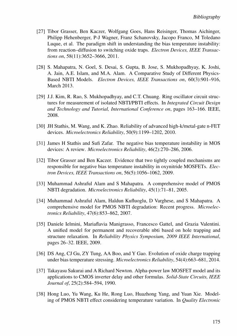
Bibliography
[27] Tibor Grasser, Ben Kaczer, Wolfgang Goes, Hans Reisinger, Thomas Aichinger,Philipp Hehenberger, P-J Wagner, Franz Schanovsky, Jacopo Franco, M ToledanoLuque, et al. The paradigm shift in understanding the bias temperature instability:from reaction–diffusion to switching oxide traps. Electron Devices, IEEE Transac-tions on, 58(11):3652–3666, 2011.
[28] S. Mahapatra, N. Goel, S. Desai, S. Gupta, B. Jose, S. Mukhopadhyay, K. Joshi,A. Jain, A.E. Islam, and M.A. Alam. A Comparative Study of Different Physics-Based NBTI Models. Electron Devices, IEEE Transactions on, 60(3):901–916,March 2013.
[29] J.J. Kim, R. Rao, S. Mukhopadhyay, and C.T. Chuang. Ring oscillator circuit struc-tures for measurement of isolated NBTI/PBTI effects. In Integrated Circuit Designand Technology and Tutorial, International Conference on, pages 163–166. IEEE,2008.
[30] JH Stathis, M. Wang, and K. Zhao. Reliability of advanced high-k/metal-gate n-FETdevices. Microelectronics Reliability, 50(9):1199–1202, 2010.
[31] James H Stathis and Sufi Zafar. The negative bias temperature instability in MOSdevices: A review. Microelectronics Reliability, 46(2):270–286, 2006.
[32] Tibor Grasser and Ben Kaczer. Evidence that two tightly coupled mechanisms areresponsible for negative bias temperature instability in oxynitride MOSFETs. Elec-tron Devices, IEEE Transactions on, 56(5):1056–1062, 2009.
[33] Muhammad Ashraful Alam and S Mahapatra. A comprehensive model of PMOSNBTI degradation. Microelectronics Reliability, 45(1):71–81, 2005.
[34] Muhammad Ashraful Alam, Haldun Kufluoglu, D Varghese, and S Mahapatra. Acomprehensive model for PMOS NBTI degradation: Recent progress. Microelec-tronics Reliability, 47(6):853–862, 2007.
[35] Daniele Ielmini, Mariaflavia Manigrasso, Francesco Gattel, and Grazia Valentini.A unified model for permanent and recoverable nbti based on hole trapping andstructure relaxation. In Reliability Physics Symposium, 2009 IEEE International,pages 26–32. IEEE, 2009.
[36] DS Ang, CJ Gu, ZY Tung, AA Boo, and Y Gao. Evolution of oxide charge trappingunder bias temperature stressing. Microelectronics Reliability, 54(4):663–681, 2014.
[37] Takayasu Sakurai and A Richard Newton. Alpha-power law MOSFET model and itsapplications to CMOS inverter delay and other formulas. Solid-State Circuits, IEEEJournal of, 25(2):584–594, 1990.
[38] Hong Luo, Yu Wang, Ku He, Rong Luo, Huazhong Yang, and Yuan Xie. Model-ing of PMOS NBTI effect considering temperature variation. In Quality Electronic
175

Bibliography
Design, 2007. ISQED’07. 8th International Symposium on, pages 139–144. IEEE,2007.
[39] M. Noda, S. Kajihara, Y. Sato, K. Miyase, X. Wen, and Y. Miura. On estimationof NBTI-Induced delay degradation. In Test Symposium (ETS), 2010 15th IEEEEuropean, pages 107 –111, May 2010.
[40] Shyh-Chyi Yang, Hao-I Yang, Ching-Te Chuang, and Wei Hwang. Timing controldegradation and NBTI/PBTI tolerant design for Write-replica circuit in nanoscaleCMOS SRAM. In VLSI Design, Automation and Test, 2009. VLSI-DAT ’09. Inter-national Symposium on, pages 162 –165, april 2009.
[41] Sanjay V. Kumar, Chris H. Kim, and Sachin S. Sapatnekar. Adaptive techniques forovercoming performance degradation due to aging in digital circuits. In Proceedingsof the 2009 Asia and South Pacific Design Automation Conference, ASP-DAC ’09,pages 284–289, Piscataway, NJ, USA, 2009. IEEE Press.
[42] Eiji Takeda, Cary Y-W Yang, and Akemi Miura-Hamada. Hot-carrier effects in MOSdevices. Academic Press, 1995.
[43] Renesas. Semiconductor Reliability Handbook. Renesas Electronics Corporation,2008.
[44] Paolo Magnone, Felice Crupi, Nicole Wils, Ruchil Jain, Hans Tuinhout, Pietro An-dricciola, Gino Giusi, and Claudio Fiegna. Impact of Hot Carriers on nMOSFETVariability in 45-and 65-nm CMOS Technologies. Electron Devices, IEEE Transac-tions on, 58(8):2347–2353, 2011.
[45] E. Takeda and N. Suzuki. An empirical model for device degradation due to hot-carrier injection. Electron Device Letters, IEEE, 4(4):111 – 113, April 1983.
[46] Mihir Choudhury, Vikas Chandra, Kartik Mohanram, and Robert Aitken. Analyticalmodel for TDDB-based performance degradation in combinational logic. In Design,Automation & Test in Europe Conference & Exhibition (DATE), 2010, pages 423–428. IEEE, 2010.
[47] A. Elhami Khorasani, M. Griswold, and T.L. Alford. A Fast I-V Screening Measure-ment for TDDB Assessment of Ultra-Thick Inter-Metal Dielectrics. Electron DeviceLetters, IEEE, 35(1):117–119, Jan 2014.
[48] David Dye. Partial Reconfiguration of Virtex FPGAs in ISE 12. Xilinx White PaperWP374, July 2010.
[49] Altera. Increasing Design Functionality with Partial and Dynamic Reconfigurationin 28-nm FPGAs. Altera White Paper WP-01137, July 2010.
[50] Rajat Chauhan and Rajesh Kaushik. Utilization of unused IO block for core logicfunctions, January 2 2007. US Patent 7,157,936 B2.
176

Bibliography
[51] E. Stott, P. Sedcole, and P. Cheung. Modelling degradation in FPGA lookup tables.In Field-Programmable Technology, 2009. FPT 2009. International Conference on,pages 443–446, dec. 2009.
[52] Edward A. Stott, Justin S.J. Wong, Pete Sedcole, and Peter Y.K. Cheung. Degrada-tion in FPGAs: measurement and modelling. In FPGA ’10: Proceedings of the 18thannual ACM/SIGDA international symposium on Field programmable gate arrays,pages 229–238, New York, NY, USA, 2010. ACM.
[53] E. Stott, J.S.J. Wong, and P.Y.K. Cheung. Degradation Analysis and Mitigation inFPGAs. In Field Programmable Logic and Applications (FPL), 2010 InternationalConference on, pages 428–433, 2010.
[54] Charles Chiasson and Vaughn Betz. Should FPGAS abandon the pass-gate? In FieldProgrammable Logic and Applications (FPL), 2013 23rd International Conferenceon, pages 1–8. IEEE, 2013.
[55] Xinfei Guo, Wayne Burleson, and Mircea Stan. Modeling and Experimental Demon-stration of Accelerated Self-Healing Techniques. In Proceedings of the The 51st An-nual Design Automation Conference on Design Automation Conference, pages 1–6.ACM, 2014.
[56] Tao Pi and Patrick J Crotty. FPGA lookup table with transmission gate structure forreliable low-voltage operation, December 23 2003. US Patent 6,667,635.
[57] Steven P Young. Programmable logic block having lookup table with partial outputsignal driving carry multiplexer, March 20 2007. US Patent 7,193,433.
[58] Predictive Technology Model (PTM). http://ptm.asu.edu/. model releasedin Oct. 2007.
[59] Xilinx. 7 Series FPGAs Configurable Logic Block. Xilinx User Guide 474, August2014.
[60] Xilinx. Spartan-6 FPGA Configurable Logic Block. Xilinx User Guide 384, Febru-ary 2010.
[61] I. Kuon, R. Tessier, and J. Rose. FPGA architecture: Survey and Challenges. Foun-dations and Trends R© in Electronic Design Automation, 2(2):135–253, 2008.
[62] G. Lemieux and D. Lewis. Circuit design of routing switches. In internationalsymposium on Field-programmable gate arrays, pages 19–28. ACM, 2002.
[63] M. Khellah, S. Brown, and Z. Vranesic. Modelling routing delays in SRAM-basedFPGAs. In Canadian Conference on VLSI, page 6B. Citeseer, 1993.
177

Bibliography
[64] Florent Bruguier, Pascal Benoit, Philippe Maurine, and Lionel Torres. A New Pro-cess Characterization Method for FPGAs Based on Electromagnetic Analysis. InFPL11 21st International Conference on Field Programmable Logic and Applica-tions, pages 20–23. Ieee, September 2011.
[65] A. Maiti, L. McDougall, and P. Schaumont. The Impact of Aging on an FPGA-BasedPhysical Unclonable Function. In International Conference on Field ProgrammableLogic and Applications (FPL), pages 151 – 156, 2011.
[66] Spartan-6 Family Overview, 2011.
[67] Florent Bruguier, Pascal Benoit, and Lionel Torres. Investigation of Digital Sensorsfor Variability Characterization on FPGAs. In Proceedings of the 5th InternationalWorkshop on Reconfigurable Communication-centric Systems on Chip 2010 Re-CoSoC10, pages 95 – 100, Karlsruhe, Germany, 2010.
[68] Tim Tuan and Bocheng Lai. Leakage power analysis of a 90nm FPGA. In CustomIntegrated Circuits Conference, 2003. Proceedings of the IEEE 2003, pages 57–60.IEEE, 2003.
[69] P. Mangalagiri, S. Bae, R. Krishnan, Y. Xie, and V. Narayanan. Thermal-awarereliability analysis for platform FPGAs. In Proceedings of the 2008 IEEE/ACMInternational Conference on Computer-Aided Design, pages 722–727. IEEE Press,2008.
[70] Jameel Hussein, Matt Klein, and Michael Hart. Lowering Power at 28 nm withXilinx 7 Series FPGAs. Xilinx White Paper WP389, Aug. 2013.
[71] S. Velusamy, Wei Huang, J. Lach, M. Stan, and K. Skadron. Monitoring temperaturein FPGA based SoCs. In Computer Design: VLSI in Computers and Processors,2005. ICCD 2005. Proceedings. 2005 IEEE International Conference on, pages 634– 637, oct. 2005.
[72] Wei Huang, K. Sankaranarayanan, K. Skadron, R.J. Ribando, and M.R. Stan. Accu-rate, Pre-RTL Temperature-Aware Design Using a Parameterized, Geometric Ther-mal Model. Computers, IEEE Transactions on, 57(9):1277 –1288, sept. 2008.
[73] Y. Yang, Z. Gu, C. Zhu, R.P. Dick, and L. Shang. Isac: Integrated space-and-time-adaptive chip-package thermal analysis. Computer-Aided Design of Integrated Cir-cuits and Systems, IEEE Transactions on, 26(1):86–99, 2007.
[74] Priya Sundararajan, Aman Gayasen, N. Vijaykrishnan, and T. Tuan. Thermal char-acterization and optimization in platform FPGAs. In Proceedings of the 2006IEEE/ACM international conference on Computer-aided design, ICCAD ’06, pages443–447, 2006.
178

Bibliography
[75] H.Y. Lui, C.H. Lee, and R.H. Patel. Power estimation and thermal budgetingmethodology for FPGAs. In Custom Integrated Circuits Conference, 2004. Pro-ceedings of the IEEE 2004, pages 711–714. IEEE, 2004.
[76] M. Happe, A. Agne, and C. Plessl. Measuring and predicting temperature distribu-tions on FPGAs at run-time. In Reconfigurable Computing and FPGAs (ReConFig),2011 International Conference on, pages 55 –60, dec. 2011.
[77] A. Amouri, H. Amrouch, T. Ebi, J. Henkel, and M. Tahoori. AccurateThermal-Profile Estimation and Validation for FPGA-Mapped Circuits. In Field-Programmable Custom Computing Machines (FCCM 2013), the 21st IEEE Interna-tional Symposium on, pages 57–60, 2013.
[78] M. DeBole, K. Ramakrishnan, V. Balakrishnan, W. Wang, H. Luo, Y. Wang, Y. Xie,Y. Cao, and N. Vijaykrishnan. A framework for estimating NBTI degradation ofmicroarchitectural components. In Design Automation Conference, 2009. ASP-DAC2009. Asia and South Pacific, pages 455–460. IEEE, 2009.
[79] CAD group. CAD Group: ITC’99 Benchmarks (2nd release), 2010.
[80] Kenneth M. Zick and John P. Hayes. On-line sensing for healthier FPGA systems. InFPGA ’10: Proceedings of the 18th annual ACM/SIGDA international symposiumon Field programmable gate arrays, pages 239–248, New York, NY, USA, 2010.ACM.
[81] Prasanth Mangalagiri, Sungmin Bae, Ramakrishnan Krishnan, Yuan Xie, and Vi-jaykrishnan Narayanan. Thermal-aware reliability analysis for platform fpgas. InICCAD ’08: Proceedings of the 2008 IEEE/ACM International Conference onComputer-Aided Design, pages 722–727, Piscataway, NJ, USA, 2008. IEEE Press.
[82] Miron Abramovici and Charles E. Stroud. BIST-Based Delay-Fault Testing in FP-GAs. J. Electron. Test., 19(5):549–558, 2003.
[83] J.S.J. Wong and P.Y.K. Cheung. Improved delay measurement method in FPGAbased on transition probability. In Proceedings of the 19th ACM/SIGDA interna-tional symposium on Field programmable gate arrays, pages 163–172. ACM, 2011.
[84] Suresh Srinivasan, Prasanth Mangalagiri, Yuan Xie, N. Vijaykrishnan, and KarthikSarpatwari. FLAW: FPGA lifetime awareness. In DAC ’06: Proceedings of the 43rdannual Design Automation Conference, pages 630–635, New York, NY, USA, 2006.ACM.
[85] John Keane, Tae hyoung Kim, Xiaofei Wang, and Chris H. Kim. On-chip reliabilitymonitors for measuring circuit degradation. Microelectronics Reliability, In Press,Corrected Proof:–, 2010.
179

Bibliography
[86] Martin Oma na, Daniele Rossi, Nicolo Bosio, and Cecilia Metra. Novel low-costaging sensor. In CF ’10: Proceedings of the 7th ACM international conference onComputing frontiers, pages 93–94, New York, NY, USA, 2010. ACM.
[87] D. Ernst, Nam Sung Kim, S. Das, S. Pant, R. Rao, Toan Pham, C. Ziesler, D. Blaauw,T. Austin, K. Flautner, and T. Mudge. Razor: a low-power pipeline based on circuit-level timing speculation. In Microarchitecture, 2003. MICRO-36. Proceedings. 36thAnnual IEEE/ACM International Symposium on, pages 7 – 18, dec. 2003.
[88] Toshinori Sato and Yuji Kunitake. A Simple Flip-Flop Circuit for Typical-CaseDesigns for DFM. In Quality Electronic Design, 2007. ISQED ’07. 8th InternationalSymposium on, pages 539 –544, mar. 2007.
[89] M. Eireiner, S. Henzler, G. Georgakos, J. Berthold, and D. Schmitt-Landsiedel.In-Situ Delay Characterization and Local Supply Voltage Adjustment for Com-pensation of Local Parametric Variations. Solid-State Circuits, IEEE Journal of,42(7):1583 –1592, jul. 2007.
[90] S. Das, C. Tokunaga, S. Pant, W.-H. Ma, S. Kalaiselvan, K. Lai, D.M. Bull, andD.T. Blaauw. RazorII: In Situ Error Detection and Correction for PVT and SERTolerance. Solid-State Circuits, IEEE Journal of, 44(1):32 –48, jan. 2009.
[91] K.A. Bowman, J.W. Tschanz, Nam Sung Kim, J.C. Lee, C.B. Wilkerson, S.-L.L.Lu, T. Karnik, and V.K. De. Energy-Efficient and Metastability-Immune ResilientCircuits for Dynamic Variation Tolerance. Solid-State Circuits, IEEE Journal of,44(1):49 –63, jan. 2009.
[92] Xilinx Synthesis and Simulation Design Guide, http://www.xilinx.com.
[93] J. Angermeier, A. Amouri, and J. Teich. General methodology for mapping iterativeapproximation algorithms to adaptive dynamically partially reconfigurable systems.In Field Programmable Logic and Applications, 2009. FPL 2009. International Con-ference on, pages 302 –307, 31 2009-sept. 2 2009.
[94] Opencores, http://opencores.org.
[95] Chunhua Yao, Kewal K Saluja, and Parameswaran Ramanathan. Thermal-aware testscheduling using on-chip temperature sensors. In VLSI Design (VLSI Design), 201124th International Conference on, pages 376–381. IEEE, 2011.
[96] Chunsheng Liu, Kugesh Veeraraghavan, and Vikram Iyengar. Thermal-aware testscheduling and hot spot temperature minimization for core-based systems. In Defectand Fault Tolerance in VLSI Systems, 2005. DFT 2005. 20th IEEE InternationalSymposium on, pages 552–560. IEEE, 2005.
[97] Zhiyuan He, Zebo Peng, Petru Eles, Paul Rosinger, and Bashir M Al-Hashimi.Thermal-aware SoC test scheduling with test set partitioning and interleaving. Jour-nal of electronic testing, 24(1-3):247–257, 2008.
180

Bibliography
[98] Justin SJ Wong, Pete Sedcole, and Peter YK Cheung. Self-measurement of combi-natorial circuit delays in FPGAs. ACM Transactions on Reconfigurable Technologyand Systems (TRETS), 2(2):10, 2009.
[99] Sergio Lopez-Buedo, Javier Garrido, and Eduardo I Boemo. Dynamically inserting,operating, and eliminating thermal sensors of FPGA-based systems. Componentsand Packaging Technologies, IEEE Transactions on, 25(4):561–566, 2002.
[100] Markus Happe, Andreas Agne, and Christian Plessl. Measuring and predicting tem-perature distributions on FPGAs at run-time. In Reconfigurable Computing andFPGAs (ReConFig), 2011 International Conference on, pages 55–60. IEEE, 2011.
[101] Adwait Gupte and Phillip Jones. Hotspot mitigation using dynamic partial reconfig-uration for improved performance. In Reconfigurable Computing and FPGAs, 2009.ReConFig’09. International Conference on, pages 89–94. IEEE, 2009.
[102] Piotr Weber, Maciej Zagrabski, Przemyslaw Musz, Krzysztof Kepa, Maciej Niko-dem, and Bartosz Wojciechowski. Configurable heat generators for FPGAs. InThermal Investigations of ICs and Systems (THERMINIC), 2014 20th InternationalWorkshop on, pages 1–4. IEEE, 2014.
[103] Andreas Agne, Hendrik Hangmann, Markus Happe, Marco Platzner, and ChristianPlessl. Seven recipes for setting your fpga on fire–a cookbook on heat generators.Microprocessors and Microsystems, 38(8):911–919, 2014.
[104] Siuki Chan and Steven HC Hsieh. Methods and apparatus for isolating critical pathson an IC device having a thermal energy generator, May 2005. US Patent 6,895,566.
[105] Steven HC Hsieh and Siuki Chan. Methods and circuits for measuring the thermalresistance of a packaged IC, Aug 2007. US Patent 7,257,511.
[106] Robert O Conn, Steven J Carey, Siuki Chan, and William H Pabst. Self-heatingmechanism for duplicating microbump failure conditions in FPGAs and for loggingfailures, Apr 2008. US Patent 7,362,121.
[107] Bradley F Dutton and Charles E Stroud. Built-in self-test of configurable logicblocks in Virtex-5 FPGAs. In System Theory, 2009. SSST 2009. 41st SoutheasternSymposium on, pages 230–234. IEEE, 2009.
[108] Xilinx. Virtex-5 FPGA User Guide. Xilinx Documentation UG190, March 2012.
[109] Doug Amos, Austin Lesea, and Rene Richter. FPGA-Based Prototyping Methodol-ogy Manual. Happy About, 2011.
[110] Jonathan Rose, Jason Luu, Chi Wai Yu, Opal Densmore, Jeff Goeders, AndrewSomerville, Kenneth B. Kent, Peter Jamieson, and Jason Anderson. The VTRProject: Architecture and CAD for FPGAs from Verilog to Routing. In Proceedingsof the 20th ACM/SIGDA International Symposium on Field-Programmable Gate Ar-rays, pages 77–86. ACM, 2012.
181

Bibliography
[111] S. Srinivasan, R. Krishnan, P. Mangalagiri, Y. Xie, V. Narayanan, M.J. Irwin, andK. Sarpatwari. Toward increasing FPGA lifetime. Dependable and Secure Comput-ing, IEEE Transactions on, 5(2):115–127, 2008.
[112] P.M.B. Rao, A. Amouri, S. Kiamehr, and M. Tahoori. Altering LUT Configurationfor Wear-out Mitigation of FPGA-Mapped Designs. In Field Programmable Logicand Applications (FPL), 2013 23nd International Conference on, pages 1–8, 2013.
182