
Digital Systems Design with PLDs and FPGAs
27
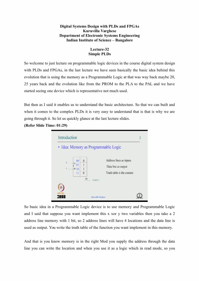
Digital Systems Design with PLDs and FPGAs Kuruvilla Varghese Department of Electronic Systems Engineering Indian Institute of Science – Bangalore Lecture-32 Simple PLDs So welcome to just lecture on programmable logic devices in the course digital system design with PLDs and FPGAs, in the last lecture we have seen basically the basic idea behind this evolution that is using the memory as a Programmable Logic at that was way back maybe 20, 25 years back and the evolution like from the PROM to the PLA to the PAL and we have started seeing one device which is representative not much used. But then as I said it enables us to understand the basic architecture. So that we can built and when it comes to the complex PLDs it is very easy to understand that is that is why we are going through it. So let us quickly glance at the last lecture slides. (Refer Slide Time: 01:29) So basic idea in a Programmable Logic device is to use memory and Programmable Logic and I said that suppose you want implement this x xor y two variables then you take a 2 address line memory with 1 bit, so 2 address lines will have 4 locations and the data line is used as output. You write the truth table of the function you want implement in this memory. And that is you know memory is in the right Mod you supply the address through the data line you can write the location and when you use it as a logic which in read mode, so you
-
Upload
khangminh22 -
Category
Documents
-
view
2 -
download
0
Transcript of Digital Systems Design with PLDs and FPGAs
Digital Systems Design with PLDs and FPGAsKuruvilla Varghese
Department of Electronic Systems EngineeringIndian Institute of Science – Bangalore
Lecture-32Simple PLDs
So welcome to just lecture on programmable logic devices in the course digital system design
with PLDs and FPGAs, in the last lecture we have seen basically the basic idea behind this
evolution that is using the memory as a Programmable Logic at that was way back maybe 20,
25 years back and the evolution like from the PROM to the PLA to the PAL and we have
started seeing one device which is representative not much used.
But then as I said it enables us to understand the basic architecture. So that we can built and
when it comes to the complex PLDs it is very easy to understand that is that is why we are
going through it. So let us quickly glance at the last lecture slides.
(Refer Slide Time: 01:29)
So basic idea in a Programmable Logic device is to use memory and Programmable Logic
and I said that suppose you want implement this x xor y two variables then you take a 2
address line memory with 1 bit, so 2 address lines will have 4 locations and the data line is
used as output. You write the truth table of the function you want implement in this memory.
And that is you know memory is in the right Mod you supply the address through the data
line you can write the location and when you use it as a logic which in read mode, so you
supply the inputs like 00 then the data line will get the 0 value when it is 0, 1 get 1 and so on.
So basically you write the truth table in a memory with the appropriate size and use the
address as input data as the output and earlier and as I said SRAM cannot be used because it
has to be program and the power on.
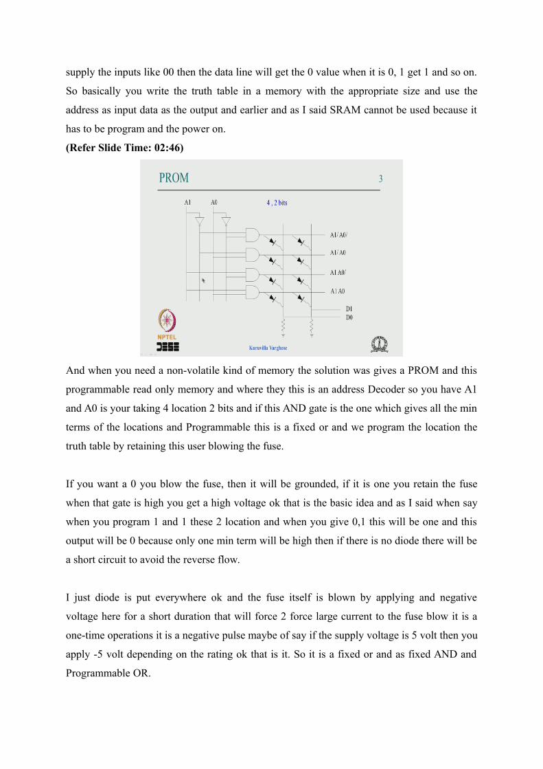
(Refer Slide Time: 02:46)
And when you need a non-volatile kind of memory the solution was gives a PROM and this
programmable read only memory and where they this is an address Decoder so you have A1
and A0 is your taking 4 location 2 bits and if this AND gate is the one which gives all the min
terms of the locations and Programmable this is a fixed or and we program the location the
truth table by retaining this user blowing the fuse.
If you want a 0 you blow the fuse, then it will be grounded, if it is one you retain the fuse
when that gate is high you get a high voltage ok that is the basic idea and as I said when say
when you program 1 and 1 these 2 location and when you give 0,1 this will be one and this
output will be 0 because only one min term will be high then if there is no diode there will be
a short circuit to avoid the reverse flow.
I just diode is put everywhere ok and the fuse itself is blown by applying and negative
voltage here for a short duration that will force 2 force large current to the fuse blow it is a
one-time operations it is a negative pulse maybe of say if the supply voltage is 5 volt then you
apply -5 volt depending on the rating ok that is it. So it is a fixed or and as fixed AND and
Programmable OR.

So n input will have 2 n vertical lines 2 n AND gates each AND gate will have the n inputs
which is connected to the appropriate lines to form the minterms, but we said that this was
kind of use for address chip select decoding where many times only one AND gate is used
even in Boolean function you do not need all the event min terms only part of them. So the
next supposed to reduce the number of AND gate and when you reduce it has to be made
Programmable cannot be fix.
That means each AND gate will have connection to all the vertical lines, all the inputs and
complements with some kind of programmability but that enables 1 to not only implement
the minterms but the product and that means you do not have to worry about A1 bar A0 bar,
in your Boolean equation if it can be minimised for some reason say you have these two
terms. And can be minimise A1 bar then you need to connect only A1 bar to the AND gate
this can be kind of though nor disconnected. So that allows us use the product term.
(Refer Slide Time: 05:44)
And that was the next step this was the basic idea of a Programmable AND where we can
program not really min terms but productive term and Programmable OR and that was call
PLA Programmable Logic array and then it turns out that if you have 3 AND gates, it is
possible to disable one AND gate by retaining all the connection. So effectively there is no
much need for this the Programmable OR with a lot of programming overhead.
(Refer Slide Time: 06:19)

So that was the next evolution to you had this was the last in the in the evolution the PAL
Programmable Array Logic where you have AND gates with Programmable connection to all
the inputs and its complement, but some fix number AND gate connected to an OR gate. So it
was possible to use if say for one to implement Boolean function of up to 3 product terms. If
you have only 2 then you disable this AND gate, so we will see that how that is done.
(Refer Slide Time: 06:53)
So that it is the evolution started with PROM which is Programmable read only memory with
a fix AND, all the 2 min terms Programmable OR your programming the content then the
Programmable AND and Programmable OR PLA which turns out that is an overkill. This can
be some are observed in this structures that was a Programmable AND and fixed OR.
(Refer Slide Time: 07:21)
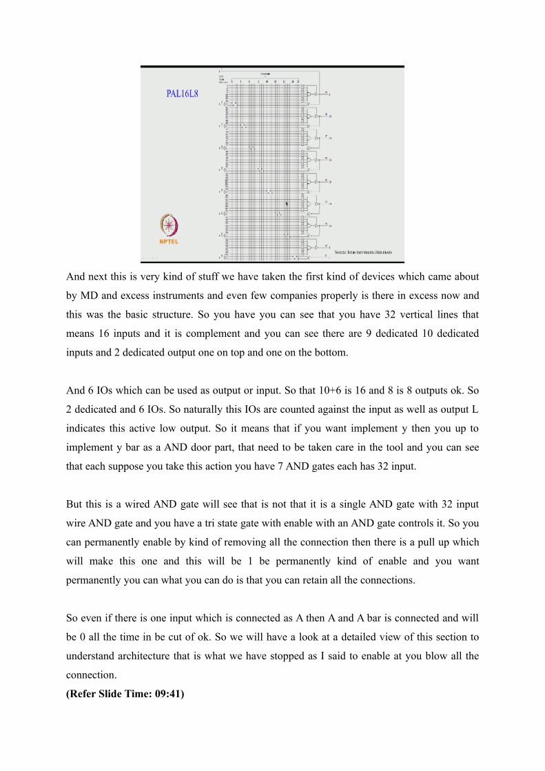
And next this is very kind of stuff we have taken the first kind of devices which came about
by MD and excess instruments and even few companies properly is there in excess now and
this was the basic structure. So you have you can see that you have 32 vertical lines that
means 16 inputs and it is complement and you can see there are 9 dedicated 10 dedicated
inputs and 2 dedicated output one on top and one on the bottom.
And 6 IOs which can be used as output or input. So that 10+6 is 16 and 8 is 8 outputs ok. So
2 dedicated and 6 IOs. So naturally this IOs are counted against the input as well as output L
indicates this active low output. So it means that if you want implement y then you up to
implement y bar as a AND door part, that need to be taken care in the tool and you can see
that each suppose you take this action you have 7 AND gates each has 32 input.
But this is a wired AND gate will see that is not that it is a single AND gate with 32 input
wire AND gate and you have a tri state gate with enable with an AND gate controls it. So you
can permanently enable by kind of removing all the connection then there is a pull up which
will make this one and this will be 1 be permanently kind of enable and you want
permanently you can what you can do is that you can retain all the connections.
So even if there is one input which is connected as A then A and A bar is connected and will
be 0 all the time in be cut of ok. So we will have a look at a detailed view of this section to
understand architecture that is what we have stopped as I said to enable at you blow all the
connection.
(Refer Slide Time: 09:41)

Then it is high you retain all the connection then the AND gate output be 0, the same
technique is used suppose you have a Boolean function with only 3 product terms, then you
implement that you know you give say this input then program the connection to implement
the various product and 1 2 3 but you do not need 4,5,6,7 what you do is that you retain all
the connections in this AND gates.
Then these will be 0 and that is kind of disable only these three will go to the because this 0
effe4ct not effect and you get a function of 3 product terms ok and this is what we have seen
last time, the structure as I said is very very elegant very useful ok. So you have a tri state
gate with enable a product on controlling that enable and the output there is looks like a
feedback to the structure.
So that adds you know that 6 add to this 10+16 and your 32, 16 inputs and its complement 32
vertical lines ok. So you should know that every AND gate has can form a product term of
any of this 32 ok, 16 and its complement and you see here now this you has multiple users ok
now obviously this can be used as output where you permanently enable this.
Then by saying blowing all the connection then this is enabled this is always an output okay.
And suppose you want used as an input then what you do is that retain all the connection then
even if there is one input at least you have to have an input to be able to use it and then the
output will be 0 this is cut off. So all this will be a waste be permanently cut off but then this
can be used as an input.

That is a case where maybe you have a circuit with more than 10 inputs say you have 12
input but your lesson number of output so that and that is good because we do not have so
many output but we need some input pins than this can be disable and it can be used as an
input ok and this goes waste of course but then you get one additional input the idea but more
than that.
You know you can be used as output it can be used as input but another option has used it as
an IO under the control of this product terms, suppose for whatever reason this is connected
to a shared bus or CPU bus for whatever logic then you suppose the CPU has a read bar so
we connect read but this signal so it is available here and we assume that read bar such is
connected to this AND gate ok.
So when the read bar is low, this is low, so this will be cut off then it is used as an input.
When the read bar is high only one input is connected, this is high and this is an output. So
naturally you know you can interface this to a processor bus need not be a processor bus,
need not be read bar it can be some product on some you can put a condition is this condition
and some other condition or some other conditions and of various condition.
Then you can implement that under that condition that will be output or input depending on
it. So it can be output, it can be input, it can be IO, but you see this if you looked at instead of
you know thinking of it as a separate thing like output or input, we can view it as this output
does coming back to this old logic ok. So it shows that this as a node can be used with you
know in the in the other along with other products.
This uses that suppose you have a Boolean function with say 20 product term then we are not
able to implement that here because always 7 product terms, so it tell us that you can have
product terms implemented in this section say the output is inverted but it does not matter it
gets second bubble second invertor there is a buffer, this line invertor in this line and that
inverter you get that signal.
And that can be connected to this fast and get here ok so you get that 7 products in this or that
you will implement supposed three additional product in this section, so you get 10 product
and so when there is a need for more than the product terms accommodated in one section

you can use this structure to cascade to get more product and so that is an additional use of
this particular structure.
Again once again this tells us in a going back tells us that this can be used as a feedback ok.
So one simple example is that you think of a cross couple NAND latch ok I hope we have
discussed this in the beginning maybe somewhere, so you have a NAND gate and 2 NAND
gates the output of 1 NAND gate divides the input of the NAND gate, it gets one set input
and this get on reset input.
This output he is feeling back the other import other name is input so by the way you think
there is an input which can be connected to one of the and gate and then get output goes to
these invertor come back through this in water goes to the input of the second hand gate and
that and get also get another input which can be connected because there are so many imports
and this goes and get double inversion and connect back to this and gets out by using two
sections.
You can implement a large if it is required ok of course there will be lot of latch twisted but it
can be done. So this allows output, input, IOs and cascading and feedback everything is kind
of made possible by just symbol you know elegant architecture. So it is quite nice and so we
will summarise this.
(Refer Slide Time: 17:06)
When an IO structure, you want use a an output have to enable the tri state gate and it is
enable by blowing all the input connections of the control AND gate which is nothing but I

call this is a control AND get which controls the enable of the tri state and which is nothing
but a wired and with pull up. So it is not AND gate with multiple input, the single wire which
is wide and we will see that how that is formed with a pull up.
So if you remove all the connection was pulled up 1 then the output is 1 and when you want
use that as an input you disable the tri sate gate retain all connections of the control AND gate
and A and A bar is kind of 0 and you can program we can use it as an IO under the control of
control product term in the control AND gate ok and you are able to pull any AND gate
suppose in the seven AND gate it in disable three of them.
If you want only use 4 by retaining all the input connection and those AND gates you can
cascade multiple section using if you have more than 7 product homes in this particular thing
you can use it as a feedback examples to form a latch so lot of you know uses for this
particular simple structure which allows us to do many things .
(Refer Slide Time: 81:45)
So I have a one point about cascading suppose you have to implement function which is an
OR of 17 product terms and sum of products there are 17 product. So way of doing is that say
in a 16 L8 kind of device is that you implement 7 product terms you like 1 2 3 up to 7, so you
ordered and what you do is that this output comes back here to double in motion and that
output is connected to one of the AND gate ok.
Then you have 6 production terms because 1 AND gate is used for cascading then you
implement a L8 6 7 plus 6 you have 30, we need 4 more, so again you take this output bring

it back here connect to the next section AND gate and the remaining 4, 4 products are
programmed in the last section disable to AND gate and this 16, pin number 16 is a Boolean
function some of the 17 product terms ok.
But there is a problem with this because if you start a look at the input hear from this input
you have one pass delay come back here then you have second pas delay then come back
here if the third pass delay and if you can imagine if there are some 25 product can view it up
one more section and you get 4 passes delay and if each passes by 5 nanosecond then you
have a 20 nanoseconds.
So there is a better way of doing it that is go on changing like that, what you do as that you
implement 7 product terms in one section 7 in a second section and this feedback comes here,
this feedback comes here now this is connected to an AND gate in third section the second
one is connected to an AND gate in this third session. So you have now 7+7 14, now the
remaining 3 product can be put in the last section.
And you get 17 product term but if you see the worst case number of passes is one like that 2
and 1 and 2 ok. So you in a 2 pass you get all kind of all possible then if you think of 7 kind
of you know AND gates in a section it possible to cascade 7 set section, you know cascaded
to an 8 section, so you will get 49 product terms in a 2 pass ok. So but if we had gone
changing like that then you have 7,6,6 you know take the same number of each section.
Then there will be 6x7 42+7+49 product term, but you see there will be 7 pass delay you
know 7 pass delay will be there, so that you should keep in mind when you when we call 2
cascade the cascade like that so, so that is.
(Refer Slide Time: 22:19)
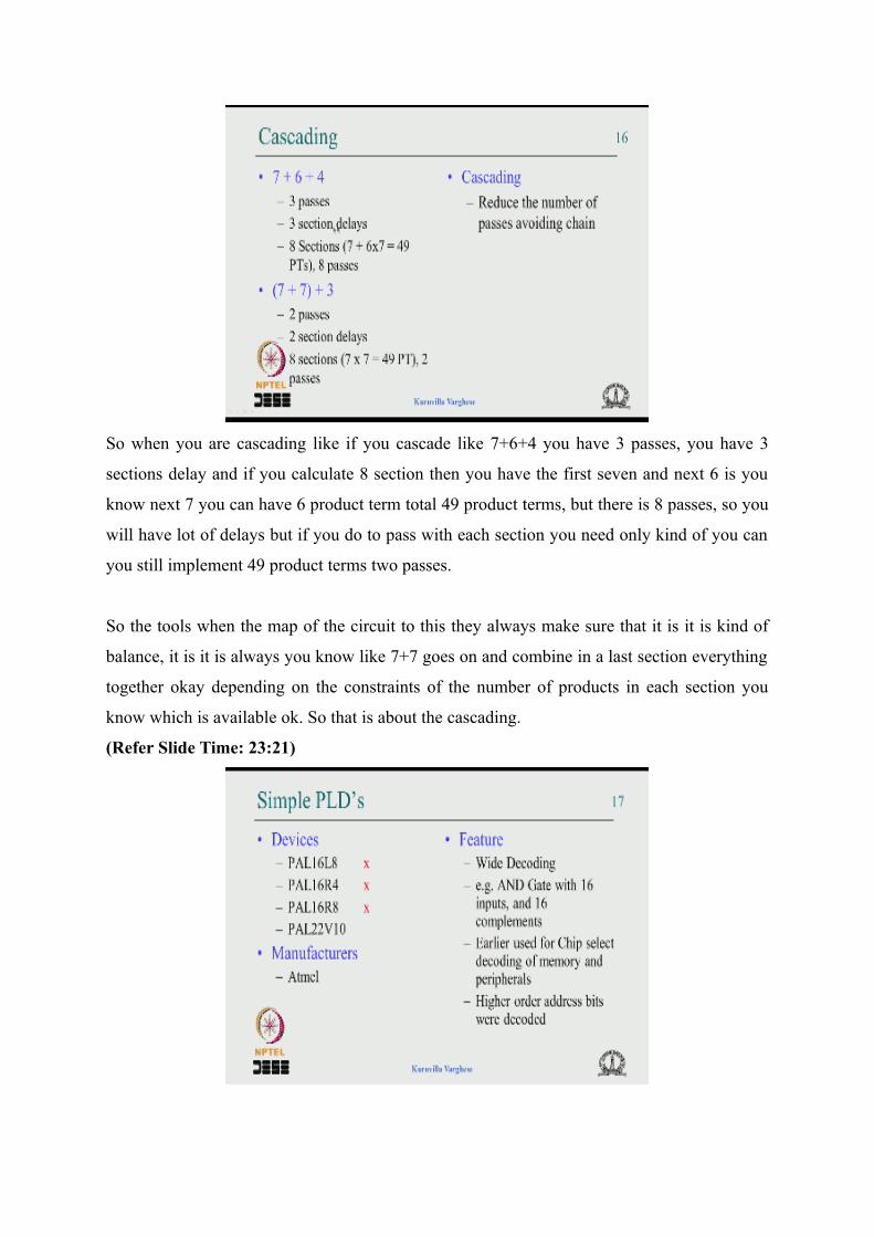
So when you are cascading like if you cascade like 7+6+4 you have 3 passes, you have 3
sections delay and if you calculate 8 section then you have the first seven and next 6 is you
know next 7 you can have 6 product term total 49 product terms, but there is 8 passes, so you
will have lot of delays but if you do to pass with each section you need only kind of you can
you still implement 49 product terms two passes.
So the tools when the map of the circuit to this they always make sure that it is it is kind of
balance, it is it is always you know like 7+7 goes on and combine in a last section everything
together okay depending on the constraints of the number of products in each section you
know which is available ok. So that is about the cascading.
(Refer Slide Time: 23:21)
Then we look at the simple PLDs at least you had something called device called PAL 16L8
which we have seen. PAL 16R4 ok now this is a device which are some registers of flip flops
and output which allows you to implement sequential circuits and data path, mainly counters
and finite state machine and 16R8 where all the output as registers and all these are not
available.
Now it is it is kind of academic inverse to understand maybe the only device which is being
used nowadays and the complex PLDs. So the PAL 22V10 is a much more flexible was like
which combines all these together you know that is that PAL 22V10 then we will see that
architecture and now the Atmel manufacturers is PAL 22V10 still may be useful in very small
processor like blue logic when you are kind of you want some kind of logic where you now
need to be Programmable.
Then you can use that it may be useful because a small amount of logic you can be put and
when you look at the simple PLDs the features of the PLDs are it allows wide decoding okay
that means that the AND gates you know 16 input and 16 of 8 compliments ok. Now it is very
rarely used it is mainly for a chip select decoding a memory and peripherals it was used.
But many application does not such as wide decoding and in a chip select decoding suppose
you have a memory of 1K or 2 K then you will use say 10 address lines rest of the address
line is decoder as a 2, 2 map it to appropriate location in the memory space and that is
decoding using the chip select Decoder ok. So that time this is useful but not anymore.
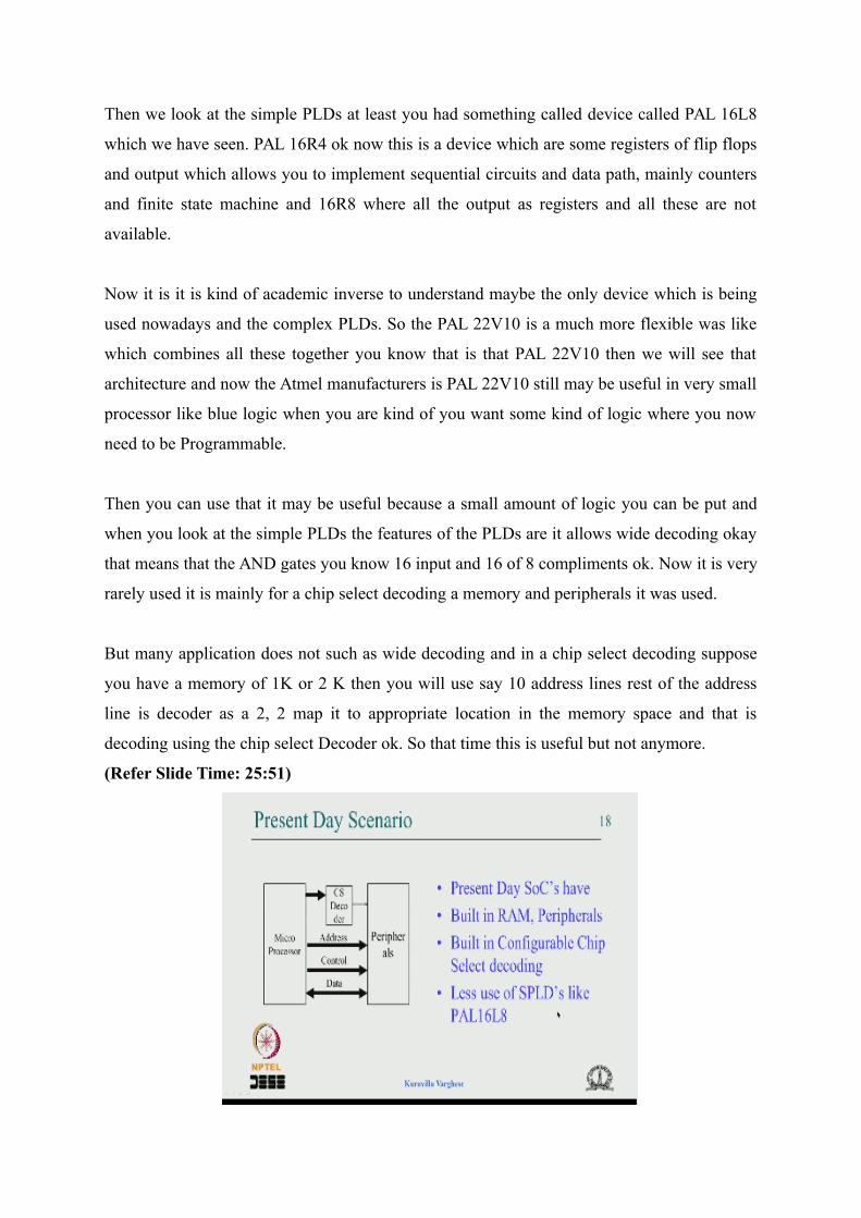
(Refer Slide Time: 25:51)

So maybe why that is not used if you analyse if you look at the earliest scenario was like this
is a microprocessor your peripherals even presently the connect I mean interfacing is similar
but earlier the memory of peripheral used to occupy a small address space and you need a
chip select decoding. So you have a data bus and a control bus like read bar write bar then
some address line depending on whether is memory peripheral this can be few or more and
chip select decoding will handle the rest of the address line ok.
So this is where the other one major use of the PAL, but now if you look at most of the
process we use are kind of resources like Emirate processes maybe the desktop processes
have some kind of additional chips one or two that they are also going into a single chip
along with the processor, so they all have the built in memory and peripherals like most of the
have built in memory and peripherals.
They also have built in configurable chip select decoding so chip select decoding is part of
the SOC, but configure you can you can change the address the memory map by configuring
it. So there is less use of SPLDs like PAL16L8 ok, so because all these are built into the
single chip and definitely not everything is built in, you need some additional peripherals like
you say take the case of Wi-Fi.
Many times that is an external kind of dongle or external peripheral but they also nowadays
whatever external peripherals are working on serial interface ok. So you have a serial clock
the processor give clock and there is a data line which is IO, so you can read or write and
address in is part of the data frame that means it possible to connect multiple peripherals
multiple slides and his mask and address through the through the data frame ok.
And even it is possible to have multiple masters controlling the peripheral and all that. So in
this scheme of things there is hardly any need for a kind of decoding, so that is why these
kind of devices are less are useful nowadays and that is effect of kind of large scale
integration of the circuit in a single step, so you must worried about this SPI or I2C which are
serial protocol which is very much use.
(Refer Slide Time: 29:06)
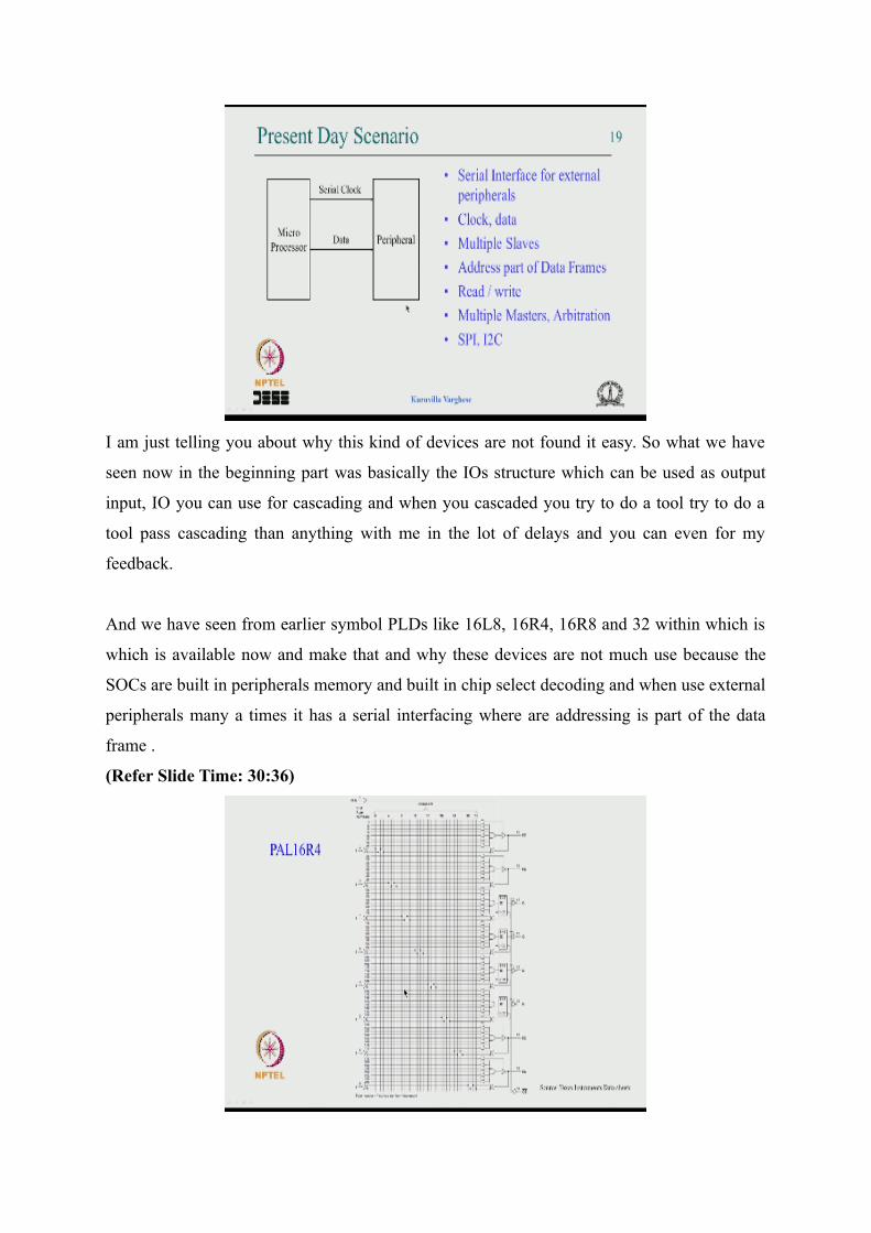
I am just telling you about why this kind of devices are not found it easy. So what we have
seen now in the beginning part was basically the IOs structure which can be used as output
input, IO you can use for cascading and when you cascaded you try to do a tool try to do a
tool pass cascading than anything with me in the lot of delays and you can even for my
feedback.
And we have seen from earlier symbol PLDs like 16L8, 16R4, 16R8 and 32 within which is
which is available now and make that and why these devices are not much use because the
SOCs are built in peripherals memory and built in chip select decoding and when use external
peripherals many a times it has a serial interfacing where are addressing is part of the data
frame .
(Refer Slide Time: 30:36)
So which kind of you know remove the need of these kind of devices. So let us look at the
next device in the line this is called 16R4 as I said this we used as a stepping stone to
understand the latter device ok. So it is pretty much similar so you have 8 sections and or
with 7 product terms with OR gate or tri state enable, so here 2 part 1 is same in single 8 to
bottom on is also same as in signal 8.
But what is different is that in the middle 4 section the output of the and or OR gate goes to a
flip flops ok, and the flop flops are clock by a pin number one which is a common clock and
the output is going through a tri state gate which is enabled by a pin ok. So this is not a much
interest we can be used if you are can connecting to a bus and this can be the control line for
reading or writing things like that.
So this is hardly of much use this you can imagine as kind of pass 2 at least to understand but
the important thing to note is that you have some kind of combinational logic proceeding I
mean preceding the flip flop or combinational logic it follows in a it follows a you know
follow the flip flop that means register and you see the Q bar of the flip flop is going back to
this, this logic section as input to the AND gate ok.
So now that tells you that if you imagine a counter in a counter architecture we have seen we
have a next state logic which decode the present state and in a complex counter you will are
various input like app download and online so it possible that with this structure now you can
have suppose you want you believe and therefore with counter you can imagine this is Q3
Q2, Q1 Q0 ok. Now all that Q3 Q2, Q1 Q0.
And their emotions are here, so if you take this D3 then D3 can be a function of Q3 Q2, Q1
Q0 any function of that up to 7 product and so it shows that you can implement a 4 bit
counter we have to be at work out the equation of the counter believe me that as far as 4 bit
counter is concern it can be implement ok, you can work out the equation and expand it, it
possible implement a 4 bit between the up counter using the structure.
Because this each section act like a next state logic which decode the present state from
various because everything is available and you are various input. So that is the next sale
logic this is the state flop with clock by a single clock ok. So this allows you to implement a

counter now ok maybe I will show some pictures of a then I will understand it is even
possible that you can implement FSM ok.
If you remember FSM is nothing but a counter with an output decode okay counter like
structure have next state logic of the present state now you know that the FSM what requires
is an output logic which Decoder present state and input. Now you take this section where all
the present state like Q0 Q1 Q2 Q3 is available here, so in principle you can use a form and
output which is decode of the Q3 Q2 Q1 Q0.
And if it is a many output you know we have various in both you can give input and you can
still decode of the inputs available because all vertical lines unavailable present states are
available here. So it can be you can form and output logic here and you get you can try to
implement FSM ok, what remained to see is a data path, data path is a register, then output of
that comes a combinational logic then follow it up the register.
So even a data path in principle can be at least there are hardly any registers we are suppose
you think of a 8 bit it is not possible but I am showing a 1 bit but maybe you can expand it to
you there were right I just reach you can think of a 4 register followed with some
computation in combination cute followed with four registers can be done in the structure.
(Refer Slide Time: 35:46)
So this is an expansion of PAL16R4 as I said their maximum input 16 because there are say
2, 2 9 which is 8+1 4 you know all these are inputs you know so there is 8+8 16 input and
registers 4 registers you know that is what the 16R4 and if you look at each section of 7

product term OR gate common clock, the OR gate or output goes to the D and Q goes as an
output.
And the Q bar is fed back it does not matter because both Q bar and it is version is available,
so it is really does not matter whether you feedback Q bar or Q its all you know depending on
what you what the device use the programming changes you know that Q is the inversion
changes that all about this device.
(Refer Slide Time: 36:53)
And if you look at a data path as I said we will see how the standard structures map to this
particular device say take a data path where you have a set of a flip-flop followed with the
combination circuits to the destination register. I will just assume that is a single bit for
convenience okay, but you can try to expand into multiple bit. So here you have some inputs
you know you can use all these input.
(Refer Slide Time: 37:22)

So input is available in this vertical lines, we have 1, 2 and its complementary 3 and its
complement now those import can be one of the input can be connected to the to the one of
the flip flop or a combination of them and you see that outputs coming back into this
structure, this array and that can be you know can be combined here to form some product
term like a combination circuit.
And that goes to the destination register and both get the same clock and you can implement
this and as I said I am just showing 1 bit but we can imagine if there are 8 register you know
you are 4 registers multiple input you combine them and this structure can be implemented
ok.
(Refer Slide Time: 38:12)

Now if you take a FSM I have already told you there are state flip flops, the present state and
input is combined in next state logic, suppose you take say Q2, Q1, Q0 then this feedback
you Q2, Q1, Q0 input will form D2, D1, D0 and the same Q2, Q1, Q0 go to some section to
generate various output.
(Refer Slide Time: 38:36)
So that is shown here so you have as I am only showing one bid say that Q0 is fed back here
but you can imagine Q1 Q2 and always available in the array and now you can form D0 as
the function of Q2, Q1, q0, so this is the next state logic this one is the next state logic and
that goes to this register. So you have input and the feedback is combined in the next state
logic.
It goes to the present state and that present status is decoded along with the input to generate
the Mealy or Moore output. So this is the next state logic and this is output logic ok. Of
course if there is a flip flop here then you can have a registered output we have discussed why
there is a requirement of a registered output when there are glitches in the output due to
translate the state that output registry.
So that is possible if you use a similar kind of section even for the output when you get
automatically the registered output and it does not matter whether you will like this 3 block
diagram or 2 block diagram it is also like if you view it like that then instead of viewing this
next state logic and output logical separate, we can view it as a single logic were part of the
logic is used for the decoding part of the logic is used as kind of output.
And that shows that you know you have a huge logic section some of it goes to the flip flop
some of it goes as an output and that is what is shown here, you have a logic and some of it
goes to the flip flops, and some of it goes direct and this is the same structure you have flip
flops fed back into an array that array combines array is logic with combined input and the
present state.
And some goes to the flip flop back some goes at the output does exactly same thing you
know you have an array where it comes is available here the feedback is available here and
some is some part is used as next state logic which goes to the to the flip flop and some part
is used as output load if it goes as a combination output exactly same thing is.
So you can say the structure of the PAL is like this which shows that the PAL kind of
structure is very useful for finite state machine. And counters and things like that, but it may
not be good as a data path because not too many flip flops ok.
(Refer Slide Time: 41:28)
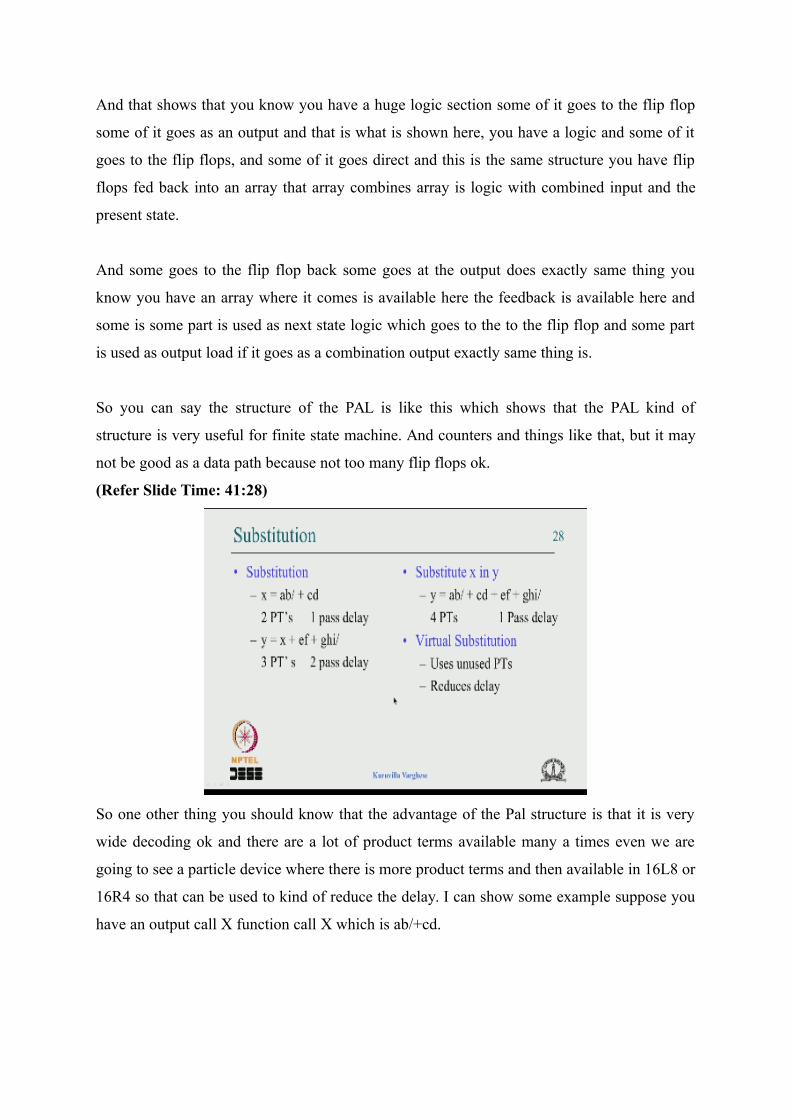
So one other thing you should know that the advantage of the Pal structure is that it is very
wide decoding ok and there are a lot of product terms available many a times even we are
going to see a particle device where there is more product terms and then available in 16L8 or
16R4 so that can be used to kind of reduce the delay. I can show some example suppose you
have an output call X function call X which is ab/+cd.
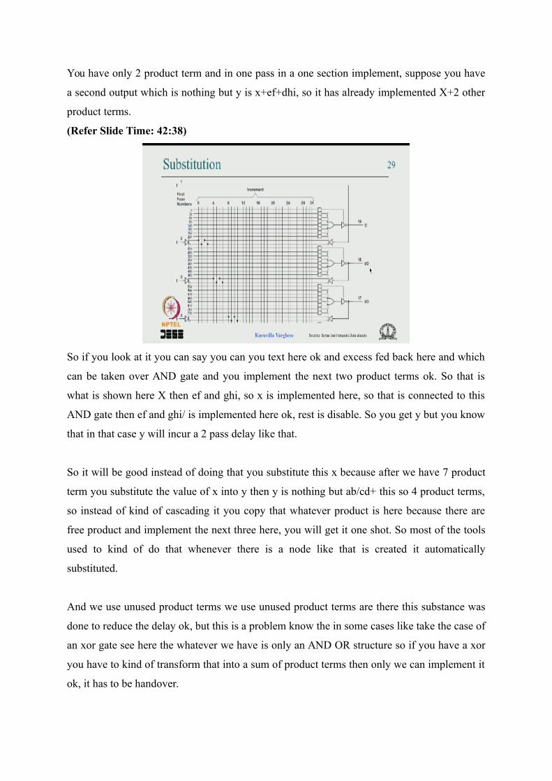
You have only 2 product term and in one pass in a one section implement, suppose you have
a second output which is nothing but y is x+ef+dhi, so it has already implemented X+2 other
product terms.
(Refer Slide Time: 42:38)
So if you look at it you can say you can you text here ok and excess fed back here and which
can be taken over AND gate and you implement the next two product terms ok. So that is
what is shown here X then ef and ghi, so x is implemented here, so that is connected to this
AND gate then ef and ghi/ is implemented here ok, rest is disable. So you get y but you know
that in that case y will incur a 2 pass delay like that.
So it will be good instead of doing that you substitute this x because after we have 7 product
term you substitute the value of x into y then y is nothing but ab/cd+ this so 4 product terms,
so instead of kind of cascading it you copy that whatever product is here because there are
free product and implement the next three here, you will get it one shot. So most of the tools
used to kind of do that whenever there is a node like that is created it automatically
substituted.
And we use unused product terms we use unused product terms are there this substance was
done to reduce the delay ok, but this is a problem know the in some cases like take the case of
an xor gate see here the whatever we have is only an AND OR structure so if you have a xor
you have to kind of transform that into a sum of product terms then only we can implement it
ok, it has to be handover.
So that is the limitation you have no xor gate, your have only AND and OR gate everything
has to be transformed into SOP form. So if you have a xor b then you will end up with ab/ or
a/b 2 product terms, but if you have a xor b xor c you can expand that it will become 4
product terms ok. So if you have up to n product terms I have shown I should have given
some indexes definitely a-n is not open ok.
But ok I hope you understand that if there are n xor like 1-2n and then you 2 raise to n-1
product terms ok and you know that the priority encoder adders and subtractor use xor and if
you do not if you do the substitution business that can be lot of kind of exponential growth of
the product comes and it cannot be accommodated like you blindly does head and then start
cascading in a waste lot of a product, lot of section and that is not good.
So many times there are attribute to turn of the virtual substitution, this substitution business
when you have this particular case pathological cases where it goes out of this situation is not
a good idea, but default most cases this substitution works very nicely other than this special
cases you can try 2 kind of expand maybe the adder equation in terms of the product terms c
and how it goes ok maybe a 4 bit adder.
(Refer Slide Time: 46:33)
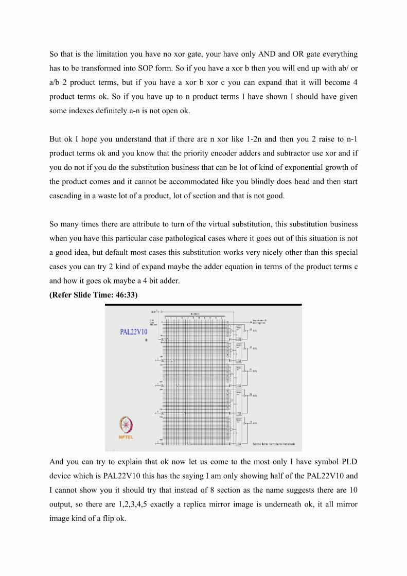
And you can try to explain that ok now let us come to the most only I have symbol PLD
device which is PAL22V10 this has the saying I am only showing half of the PAL22V10 and
I cannot show you it should try that instead of 8 section as the name suggests there are 10
output, so there are 1,2,3,4,5 exactly a replica mirror image is underneath ok, it all mirror
image kind of a flip ok.
It is a vertical flip of this is down below and you see the so there are 10 section and the first
thing you notice is that the number of product terms of variable okay the previous devices we
have seen that there are 7 product terms but here the top section as 8, 10, 12, 14 and 16 ok
and then again back 16 12 14 10 8 know so that is how it goes 8 10 12 14 16 when you come
here is a lot of lot of product ok.
Now you see there are 22 input that means there are 12 inputs, 10 IOs, so these are 5 section,
5 section is below then IO so that 10+12 is 22 input maximum and these IOs can be used as
output for 10 output and this V shows you notice that it is variable product term ok. Now the
next thing is that you have basically a flip flop with some additional circuit ok. We will see
what is inside there here and is call macrocell.
Because it is there are more than a flip flop, it is a macro which include with flip flop many
other things. So you have a clock in a pin which can be used as clock for all the macrocell or
all the flip flop. Now before even going to the detail of this section I want to say that if you
want it use this as a combinational section that means you do not want the AND or output to
go to a flip flop and unregistered output of the from you want it directly there is a must inside
by which we can bypass that flip flop.
So suppose in some particular application it is completely combination application there is no
sequential element then you will be bypassing all the macrocell in that case this clock input is
a waste. So you can see that that clock is available as an input, so not used as a clock it can be
used as an input for a combination input ok, maybe there is a less used for clock as an input
to design review AND the cock with something which in a proper synchronous design may
not are much use.
So this is given as an input if all the sections used as a combinational section ok. So this is a
micro cell which includes of the flop also include a bypass ok. Now you can see that the
feedback here you can come from two places internally you come only it can come from the
flip flop but if given by passing the flip flop then that feedback is not useful, then this pin is
feedback.

In that case you know like 16L8 you can be used as output input IO cascading all that applies.
So it say you can say it is a combination of a 16L8 and 16R8 kind of structure everything put
that kind of advantage of this 22V10 very flexible it combines all those functionality you do
not need an additional device probably that is why this device at least manufacturers are
making this device it kind of combine all the advantages of the earlier devices ok.
So that is the device and you see similarly you have that tri state gate and enable by a control
product term, but in addition to you should not that at the top is an AND gate which can be a
kind of decoding of all the 20 inputs or its complement and that goes to the asynchronous
reset of the register. So you can in principle say give a reset signal here and you can reset at
the power on all the y know all the flip flops.
And it may not be a simple reset it can be a combination of condition like your multiple
condition and depending on those conditioner can reset a similarly likely which is not shown
in the picture is another AND gate it comes at the bottom of the device at lease in the
schematic I do not know the real device that comes at the bottom but in the picture it comes
at the bottom.
So that is an AND gate the output of which goes to the synchronous preset of all the flip flop,
so if that is 1 then the next clock all the flip flops all the outputs are set 1 and here as soon as
it is asserted it is reset ok. So I hope you get an idea of the kind of flexibility of the device a
variable product comes 8, 10, 12, 14 and 16 and a replica you have 12 dedicated input, 10 IOs
and 10 macro cell.
The flip flop gets a clock and macro cell allow by passing the flop and there is a feedback
from the flip flop or the combinational section, there is an AND gate for asynchronous reset,
there is an AND gate for synchronous reset ok. So now let us look at this micro cell which is
shown here.
(Refer Slide Time: 53:21)

That in the spot ok, so this is the AND gate which is the top 1 which is controlling the tri state
gate this is the say if you take the top section, so there are 8 product terms OR gate, that goes
to flip flop and this is a clock this is asynchronous reset the synchronous set ok and you see
here there is a 4 to 1 mux ok there are two select which is pulled up and connected to a fuse
ok.
So by retaining the fuse both are kind of 00, if blow 1 say 0 then you get 0,1, so by blowing
retaining the fuse you can choose 0,0,0 1,1,0,1,1, so you can choose any of this and you see
here you have the possibility of this output or its complement coming here or the Q or Q bar
come here ok. So you might wonder why that is required because either you need is output or
the registered version, but this scheme allows some optimisation.
Because suppose you have to implement y ok, sum of product terms now you know that if
you have to do that there is an inversion here. So one way doing is that you implement y and
then you select a path like that, so you get the y ok and it comes like that y bar and one more
inversion you get the y ok. But assume that say y when you try to implement you and up with
say 12 product it cannot be implemented in 8 AND gates.
Suppose you take y bar it turns out that it is kind of minimise into 7 product, you apply De
Morgan theorem, then you end up with 7 product. So at that time you implement y bar ok and
use this path then y bar is not in bit y, so depending on whether y is implemented y bar is
implemented here, you can whichever is less number of products you can choose you know it
is y then this part y bar you take this path ok.
Same thing applies to the Q and Q bar ok. So this kind of structure allows you kind of a
product minimization ok, it is a great thing nowadays may not be a big thing but at the time
of these devices available that kind of saving was very great and you can see them depending
on this fuse you can you get a feedback because this is a 1, so if it is fine if it is blown 1 then
these two parts are selected.
That means the flip flop is selected, so this blown then you choose this path you know you
you choose this path otherwise it is 0, this particular combinational path is chosen depending
on when you choose this 2 path this is a path goes to the feedback mark when you do this 2
paths output then this is the feedback because this is like a 16R4. So I hope you understand
now the architecture of 22V10.
Very quickly I want to summarise here, of variable reluctance asynchronous set product and
synchronous product term, you have combinational or registered output, you have product
term optimisation by inversion, so I am showing in examples this y as 4 product terms and
when you take y bar you kind of applied De Morgan theorem then you end up with two
products and there is a time maybe we will talk about this timing in the next lecture.
So you have for propagation delay you have you know how to enable and disable timing and
the flip flop delay tcq, set up and whole time and the reset delay and all that these are the
other kind of timing parameters in the case of 16L8 itself, 1 section delay, there is nothing
more to it. So I think you have you looked at the 22V20 the most versatile useful device
which is even available today.
It combines a combinational and the registered part time both 16L8 and 16R8 you can use it
as a combination of registered, so you have all possibilities you can implement logic and
implement FSM you can implement counter, you can even have know registered output or
combinational output for finite state machine. So it is quiet and you have the largest section
of 16 product terms you have reset available, preset available.
So quite a useful device, so this only simple PLD which is available we will now look I think
in the next lectures we can go to the complex PLD having understood this. So I think I stop

here this part of the lecture, please revise try to understand this architecture well, so I wish
you all the best and thank you.