Digital Systems and Binary Numbers
72
1 Chapter 1 Digital Systems and Binary Numbers 1.1 DIGITAL SYSTEMS Digital systems have such a prominent role in everyday life that we refer to the present technological period as the digital age. Digital systems are used in communication, busi- ness transactions, traffic control, spacecraft guidance, medical treatment, weather mon- itoring, the Internet, and many other commercial, industrial, and scientific enterprises. We have digital telephones, digital televisions, digital versatile discs, digital cameras, handheld devices, and, of course, digital computers. We enjoy music downloaded to our portable media player (e.g., iPod Touch™) and other handheld devices having high‐ resolution displays. These devices have graphical user interfaces (GUIs), which enable them to execute commands that appear to the user to be simple, but which, in fact, involve precise execution of a sequence of complex internal instructions. Most, if not all, of these devices have a special‐purpose digital computer embedded within them. The most striking property of the digital computer is its generality. It can follow a sequence of instructions, called a program, that operates on given data. The user can specify and change the program or the data according to the specific need. Because of this flexibil- ity, general‐purpose digital computers can perform a variety of information‐processing tasks that range over a wide spectrum of applications. One characteristic of digital systems is their ability to represent and manipulate dis- crete elements of information. Any set that is restricted to a finite number of elements contains discrete information. Examples of discrete sets are the 10 decimal digits, the 26 letters of the alphabet, the 52 playing cards, and the 64 squares of a chessboard. Early digital computers were used for numeric computations. In this case, the discrete ele- ments were the digits. From this application, the term digital computer emerged. Dis- crete elements of information are represented in a digital system by physical quantities
-
Upload
khangminh22 -
Category
Documents
-
view
5 -
download
0
Transcript of Digital Systems and Binary Numbers

1
Chapter 1
Digital Systems and Binary Numbers
1 . 1 D I G I TA L S Y S T E M S
Digital systems have such a prominent role in everyday life that we refer to the present
technological period as the digital age. Digital systems are used in communication, busi-
ness transactions, traffic control, spacecraft guidance, medical treatment, weather mon-
itoring, the Internet, and many other commercial, industrial, and scientific enterprises.
We have digital telephones, digital televisions, digital versatile discs, digital cameras,
handheld devices, and, of course, digital computers. We enjoy music downloaded to our
portable media player (e.g., iPod Touch™) and other handheld devices having high‐
resolution displays. These devices have graphical user interfaces (GUIs), which enable
them to execute commands that appear to the user to be simple, but which, in fact,
involve precise execution of a sequence of complex internal instructions. Most, if not all,
of these devices have a special‐purpose digital computer embedded within them. The
most striking property of the digital computer is its generality. It can follow a sequence
of instructions, called a program, that operates on given data. The user can specify and
change the program or the data according to the specific need. Because of this flexibil-
ity, general‐purpose digital computers can perform a variety of information‐processing
tasks that range over a wide spectrum of applications.
One characteristic of digital systems is their ability to represent and manipulate dis-
crete elements of information. Any set that is restricted to a finite number of elements
contains discrete information. Examples of discrete sets are the 10 decimal digits, the
26 letters of the alphabet, the 52 playing cards, and the 64 squares of a chessboard. Early
digital computers were used for numeric computations. In this case, the discrete ele-
ments were the digits. From this application, the term digital computer emerged. Dis-
crete elements of information are represented in a digital system by physical quantities

2 Chapter 1 Digital Systems and Binary Numbers
called signals. Electrical signals such as voltages and currents are the most common.
Electronic devices called transistors predominate in the circuitry that implements these
signals. The signals in most present‐day electronic digital systems use just two discrete
values and are therefore said to be binary. A binary digit, called a bit, has two values: 0
and 1. Discrete elements of information are represented with groups of bits called binary
codes. For example, the decimal digits 0 through 9 are represented in a digital system
with a code of four bits (e.g., the number 7 is represented by 0111). How a pattern of
bits is interpreted as a number depends on the code system in which it resides. To make
this distinction, we could write (0111) 2 to indicate that the pattern 0111 is to be inter-
preted in a binary system, and (0111) 10 to indicate that the reference system is decimal.
Then 0111 2 = 7 10 , which is not the same as 0111 10 , or one hundred eleven. The subscript
indicating the base for interpreting a pattern of bits will be used only when clarification
is needed. Through various techniques, groups of bits can be made to represent discrete
symbols, not necessarily numbers, which are then used to develop the system in a digital
format. Thus, a digital system is a system that manipulates discrete elements of informa-
tion represented internally in binary form. In today’s technology, binary systems are most
practical because, as we will see, they can be implemented with electronic components.
Discrete quantities of information either emerge from the nature of the data being
processed or may be quantized from a continuous process. On the one hand, a payroll
schedule is an inherently discrete process that contains employee names, social security
numbers, weekly salaries, income taxes, and so on. An employee’s paycheck is processed
by means of discrete data values such as letters of the alphabet (names), digits (salary),
and special symbols (such as $). On the other hand, a research scientist may observe a
continuous process, but record only specific quantities in tabular form. The scientist is
thus quantizing continuous data, making each number in his or her table a discrete
quantity. In many cases, the quantization of a process can be performed automatically
by an analog‐to‐digital converter, a device that forms a digital (discrete) representation
of a analog (continuous) quantity.
The general‐purpose digital computer is the best‐known example of a digital system.
The major parts of a computer are a memory unit, a central processing unit, and input–
output units. The memory unit stores programs as well as input, output, and intermedi-
ate data. The central processing unit performs arithmetic and other data‐processing
operations as specified by the program. The program and data prepared by a user are
transferred into memory by means of an input device such as a keyboard. An output
device, such as a printer, receives the results of the computations, and the printed results
are presented to the user. A digital computer can accommodate many input and output
devices. One very useful device is a communication unit that provides interaction with
other users through the Internet. A digital computer is a powerful instrument that can
perform not only arithmetic computations, but also logical operations. In addition, it can
be programmed to make decisions based on internal and external conditions.
There are fundamental reasons that commercial products are made with digital cir-
cuits. Like a digital computer, most digital devices are programmable. By changing the
program in a programmable device, the same underlying hardware can be used for many
different applications, thereby allowing its cost of development to be spread across a
wider customer base. Dramatic cost reductions in digital devices have come about

Section 1.2 Binary Numbers 3
because of advances in digital integrated circuit technology. As the number of transistors
that can be put on a piece of silicon increases to produce complex functions, the cost per
unit decreases and digital devices can be bought at an increasingly reduced price. Equip-
ment built with digital integrated circuits can perform at a speed of hundreds of millions
of operations per second. Digital systems can be made to operate with extreme reli-
ability by using error‐correcting codes. An example of this strategy is the digital versa-
tile disk (DVD), in which digital information representing video, audio, and other data
is recorded without the loss of a single item. Digital information on a DVD is recorded
in such a way that, by examining the code in each digital sample before it is played back,
any error can be automatically identified and corrected.
A digital system is an interconnection of digital modules. To understand the opera-tion of each digital module, it is necessary to have a basic knowledge of digital circuits and their logical function. The first seven chapters of this book present the basic tools
of digital design, such as logic gate structures, combinational and sequential circuits, and
programmable logic devices. Chapter 8 introduces digital design at the register transfer
level (RTL) using a modern hardware description language (HDL). Chapter 9 concludes
the text with laboratory exercises using digital circuits.
A major trend in digital design methodology is the use of a HDL to describe and simulate
the functionality of a digital circuit. An HDL resembles a programming language and is
suitable for describing digital circuits in textual form. It is used to simulate a digital system
to verify its operation before hardware is built. It is also used in conjunction with logic syn-
thesis tools to automate the design process. Because it is important that students become familiar with an HDL‐based design methodology , HDL descriptions of digital circuits are
presented throughout the book. While these examples help illustrate the features of an HDL,
they also demonstrate the best practices used by industry to exploit HDLs. Ignorance of
these practices will lead to cute, but worthless, HDL models that may simulate a phenom-
enon, but that cannot be synthesized by design tools, or to models that waste silicon area or
synthesize to hardware that cannot operate correctly.
As previously stated, digital systems manipulate discrete quantities of information
that are represented in binary form. Operands used for calculations may be expressed
in the binary number system. Other discrete elements, including the decimal digits and
characters of the alphabet, are represented in binary codes. Digital circuits, also referred
to as logic circuits, process data by means of binary logic elements (logic gates) using
binary signals. Quantities are stored in binary (two‐valued) storage elements (flip‐flops).
The purpose of this chapter is to introduce the various binary concepts as a frame of
reference for further study in the succeeding chapters.
1 . 2 B I N A RY N U M B E R S
A decimal number such as 7,392 represents a quantity equal to 7 thousands, plus 3 hun-
dreds, plus 9 tens, plus 2 units. The thousands, hundreds, etc., are powers of 10 implied
by the position of the coefficients (symbols) in the number. To be more exact, 7,392 is a
shorthand notation for what should be written as
7 * 103 + 3 * 102 + 9 * 101 + 2 * 100

4 Chapter 1 Digital Systems and Binary Numbers
However, the convention is to write only the numeric coefficients and, from their posi-
tion, deduce the necessary powers of 10 with powers increasing from right to left. In
general, a number with a decimal point is represented by a series of coefficients:
a5a4a3a2a1a0. a-1a-2a-3
The coefficients aj are any of the 10 digits (0, 1, 2, c , 9), and the subscript value j gives
the place value and, hence, the power of 10 by which the coefficient must be multiplied.
Thus, the preceding decimal number can be expressed as
105a5 + 104a4 + 103a3 + 102a2 + 101a1 + 100a0 + 10-1a-1 + 10-2a-2 + 10-3a-3
with a 3 = 7, a 2 = 3, a 1 = 9, and a 0 = 2.
The decimal number system is said to be of base, or radix, 10 because it uses 10 digits
and the coefficients are multiplied by powers of 10. The binary system is a different
number system. The coefficients of the binary number system have only two possible
values: 0 and 1. Each coefficient aj is multiplied by a power of the radix, e.g., 2j, and
the results are added to obtain the decimal equivalent of the number. The radix
point (e.g., the decimal point when 10 is the radix) distinguishes positive powers of
10 from negative powers of 10. For example, the decimal equivalent of the binary
number 11010.11 is 26.75, as shown from the multiplication of the coefficients by
powers of 2:
1 * 24 + 1 * 23 + 0 * 22 + 1 * 21 + 0 * 20 + 1 * 2-1 + 1 * 2-2 = 26.75
There are many different number systems. In general, a number expressed in a base‐r
system has coefficients multiplied by powers of r:
an # rn + an -1# rn -1 + g + a2
# r2 + a1# r + a0 + a-1
# r-1
+ a-2# r-2 + g + a-m # r-m
The coefficients aj range in value from 0 to r - 1. To distinguish between numbers of
different bases, we enclose the coefficients in parentheses and write a subscript equal to
the base used (except sometimes for decimal numbers, where the content makes it obvi-
ous that the base is decimal). An example of a base‐5 number is
(4021.2)5 = 4 * 53 + 0 * 52 + 2 * 51 + 1 * 50 + 2 * 5-1 = (511.4)10
The coefficient values for base 5 can be only 0, 1, 2, 3, and 4. The octal number system
is a base‐8 system that has eight digits: 0, 1, 2, 3, 4, 5, 6, 7. An example of an octal number
is 127.4. To determine its equivalent decimal value, we expand the number in a power
series with a base of 8:
(127.4)8 = 1 * 82 + 2 * 81 + 7 * 80 + 4 * 8-1 = (87.5)10
Note that the digits 8 and 9 cannot appear in an octal number.
It is customary to borrow the needed r digits for the coefficients from the decimal
system when the base of the number is less than 10. The letters of the alphabet are used to supplement the 10 decimal digits when the base of the number is greater than 10. For
example, in the hexadecimal (base‐16) number system, the first 10 digits are borrowed

Section 1.2 Binary Numbers 5
from the decimal system. The letters A, B, C, D, E, and F are used for the digits 10, 11,
12, 13, 14, and 15, respectively. An example of a hexadecimal number is
(B65F)16 = 11 * 163 + 6 * 162 + 5 * 161 + 15 * 160 = (46,687)10
The hexadecimal system is used commonly by designers to represent long strings of bits
in the addresses, instructions, and data in digital systems. For example, B65F is used to
represent 1011011001010000.
As noted before, the digits in a binary number are called bits. When a bit is equal to
0, it does not contribute to the sum during the conversion. Therefore, the conversion
from binary to decimal can be obtained by adding only the numbers with powers of two
corresponding to the bits that are equal to 1. For example,
(110101)2 = 32 + 16 + 4 + 1 = (53)10
There are four 1’s in the binary number. The corresponding decimal number is the sum
of the four powers of two. Zero and the first 24 numbers obtained from 2 to the power of
n are listed in Table 1.1 . In computer work, 210 is referred to as K (kilo), 220 as M (mega),
230 as G (giga), and 240 as T (tera). Thus, 4K = 212 = 4,096 and 16M = 224 = 16,777,216.
Computer capacity is usually given in bytes. A byte is equal to eight bits and can accom-
modate (i.e., represent the code of) one keyboard character. A computer hard disk with
four gigabytes of storage has a capacity of 4G = 232 bytes (approximately 4 billion bytes).
A terabyte is 1024 gigabytes, approximately 1 trillion bytes.
Arithmetic operations with numbers in base r follow the same rules as for decimal
numbers. When a base other than the familiar base 10 is used, one must be careful to
use only the r‐allowable digits. Examples of addition, subtraction, and multiplication of
two binary numbers are as follows:
augend: 101101 minuend: 101101 multiplicand: 1011
addend: +100111 subtrahend: -100111 multiplier: * 101
sum: 1010100 difference: 000110 1011
0000
1011
product: 110111
Table 1.1 Powers of Two
n 2n n 2n n 2n
0 1 8 256 16 65,536
1 2 9 512 17 131,072
2 4 10 1,024 (1K) 18 262,144
3 8 11 2,048 19 524,288
4 16 12 4,096 (4K) 20 1,048,576 (1M)
5 32 13 8,192 21 2,097,152
6 64 14 16,384 22 4,194,304
7 128 15 32,768 23 8,388,608
partial product:

6 Chapter 1 Digital Systems and Binary Numbers
The sum of two binary numbers is calculated by the same rules as in decimal, except
that the digits of the sum in any significant position can be only 0 or 1. Any carry
obtained in a given significant position is used by the pair of digits one significant posi-
tion higher. Subtraction is slightly more complicated. The rules are still the same as in
decimal, except that the borrow in a given significant position adds 2 to a minuend digit.
(A borrow in the decimal system adds 10 to a minuend digit.) Multiplication is simple:
The multiplier digits are always 1 or 0; therefore, the partial products are equal either
to a shifted (left) copy of the multiplicand or to 0.
1 . 3 N U M B E R ‐ B A S E C O N V E R S I O N S
Representations of a number in a different radix are said to be equivalent if they have
the same decimal representation. For example, (0011) 8 and (1001) 2 are equivalent—both
have decimal value 9. The conversion of a number in base r to decimal is done by
expanding the number in a power series and adding all the terms as shown previously.
We now present a general procedure for the reverse operation of converting a decimal
number to a number in base r. If the number includes a radix point, it is necessary to
separate the number into an integer part and a fraction part, since each part must be
converted differently. The conversion of a decimal integer to a number in base r is done
by dividing the number and all successive quotients by r and accumulating the remain-
ders. This procedure is best illustrated by example.
EXAMPLE 1.1
Convert decimal 41 to binary. First, 41 is divided by 2 to give an integer quotient of 20
and a remainder of 12. Then the quotient is again divided by 2 to give a new quotient and
remainder. The process is continued until the integer quotient becomes 0. The coefficients
of the desired binary number are obtained from the remainders as follows:
Integer Quotient
Remainder Coefficient
41>2 = 20 + 12 a0 = 1
20>2 = 10 + 0 a1 = 0
10>2 = 5 + 0 a2 = 0
5>2 = 2 + 12 a3 = 1
2>2 = 1 + 0 a4 = 0
1>2 = 0 + 12 a5 = 1
Therefore, the answer is (41)10 = (a5a4a3a2a1a0)2 = (101001)2.

Section 1.3 Number‐Base Conversions 7
The arithmetic process can be manipulated more conveniently as follows:
Integer Remainder
41
20 1
10 0
5 0
2 1
1 0
0 1 101001 = answer
Conversion from decimal integers to any base‐r system is similar to this example, except
that division is done by r instead of 2.
■
EXAMPLE 1.2
Convert decimal 153 to octal. The required base r is 8. First, 153 is divided by 8 to give
an integer quotient of 19 and a remainder of 1. Then 19 is divided by 8 to give an integer
quotient of 2 and a remainder of 3. Finally, 2 is divided by 8 to give a quotient of 0 and
a remainder of 2. This process can be conveniently manipulated as follows:
153
19 1
2 3
0 2 = (231)8
The conversion of a decimal fraction to binary is accomplished by a method similar
to that used for integers. However, multiplication is used instead of division, and integers
instead of remainders are accumulated. Again, the method is best explained by example.
■
EXAMPLE 1.3
Convert (0.6875)10 to binary. First, 0.6875 is multiplied by 2 to give an integer and a fraction.
Then the new fraction is multiplied by 2 to give a new integer and a new fraction. The process
is continued until the fraction becomes 0 or until the number of digits has sufficient
accuracy. The coefficients of the binary number are obtained from the integers as follows:
Integer Fraction Coefficient
0.6875 * 2 = 1 + 0.3750 a-1 = 1
0.3750 * 2 = 0 + 0.7500 a-2 = 0
0.7500 * 2 = 1 + 0.5000 a-3 = 1
0.5000 * 2 = 1 + 0.0000 a-4 = 1

8 Chapter 1 Digital Systems and Binary Numbers
Therefore, the answer is (0.6875)10 = (0. a-1 a-2 a-3 a-4)2 = (0.1011)2.
To convert a decimal fraction to a number expressed in base r, a similar procedure is
used. However, multiplication is by r instead of 2, and the coefficients found from the
integers may range in value from 0 to r - 1 instead of 0 and 1.
■
EXAMPLE 1.4
Convert (0.513)10 to octal.
0.513 * 8 = 4.104
0.104 * 8 = 0.832
0.832 * 8 = 6.656
0.656 * 8 = 5.248
0.248 * 8 = 1.984
0.984 * 8 = 7.872
The answer, to seven significant figures, is obtained from the integer part of the products:
(0.513)10 = (0.406517c )8
The conversion of decimal numbers with both integer and fraction parts is done by
converting the integer and the fraction separately and then combining the two answers.
Using the results of Examples 1.1 and 1.3, we obtain
(41.6875)10 = (101001.1011)2
From Examples 1.2 and 1.4, we have
(153.513)10 = (231.406517)8
■
1 . 4 O C TA L A N D H E X A D E C I M A L N U M B E R S
The conversion from and to binary, octal, and hexadecimal plays an important role in digi-
tal computers, because shorter patterns of hex characters are easier to recognize than long
patterns of 1’s and 0’s. Since 23 = 8 and 24 = 16, each octal digit corresponds to three
binary digits and each hexadecimal digit corresponds to four binary digits. The first 16 num-
bers in the decimal, binary, octal, and hexadecimal number systems are listed in Table 1.2 .
The conversion from binary to octal is easily accomplished by partitioning the binary
number into groups of three digits each, starting from the binary point and proceeding
to the left and to the right. The corresponding octal digit is then assigned to each group.
The following example illustrates the procedure:
(10 110 001 101 011 # 111 100 000 110)2 = (26153.7406)8
2 6 1 5 3 7 4 0 6

Section 1.4 Octal and Hexadecimal Numbers 9
Conversion from binary to hexadecimal is similar, except that the binary number is
divided into groups of four digits:
(10 1100 0110 1011 # 1111 0010)2 = (2C6B.F2)16
2 C 6 B F 2
The corresponding hexadecimal (or octal) digit for each group of binary digits is easily
remembered from the values listed in Table 1.2 .
Conversion from octal or hexadecimal to binary is done by reversing the preceding
procedure. Each octal digit is converted to its three‐digit binary equivalent. Similarly,
each hexadecimal digit is converted to its four‐digit binary equivalent. The procedure is
illustrated in the following examples:
(673.124)8 = (110 111 011 # 001 010 100)2
6 7 3 1 2 4
and
(306.D)16 = (0011 0000 0110 # 1101)2
3 0 6 D
Binary numbers are difficult to work with because they require three or four times
as many digits as their decimal equivalents. For example, the binary number 111111111111
is equivalent to decimal 4095. However, digital computers use binary numbers, and it is
sometimes necessary for the human operator or user to communicate directly with the
Table 1.2 Numbers with Different Bases
Decimal (base 10)
Binary (base 2)
Octal (base 8)
Hexadecimal (base 16)
00 0000 00 0
01 0001 01 1
02 0010 02 2
03 0011 03 3
04 0100 04 4
05 0101 05 5
06 0110 06 6
07 0111 07 7
08 1000 10 8
09 1001 11 9
10 1010 12 A
11 1011 13 B
12 1100 14 C
13 1101 15 D
14 1110 16 E
15 1111 17 F

10 Chapter 1 Digital Systems and Binary Numbers
machine by means of such numbers. One scheme that retains the binary system in the
computer, but reduces the number of digits the human must consider, utilizes the rela-
tionship between the binary number system and the octal or hexadecimal system. By this
method, the human thinks in terms of octal or hexadecimal numbers and performs the
required conversion by inspection when direct communication with the machine is nec-
essary. Thus, the binary number 111111111111 has 12 digits and is expressed in octal as
7777 (4 digits) or in hexadecimal as FFF (3 digits). During communication between
people (about binary numbers in the computer), the octal or hexadecimal representa-
tion is more desirable because it can be expressed more compactly with a third or a
quarter of the number of digits required for the equivalent binary number. Thus, most computer manuals use either octal or hexadecimal numbers to specify binary quantities . The choice between them is arbitrary, although hexadecimal tends to win out, since it
can represent a byte with two digits.
1 . 5 C O M P L E M E N T S O F N U M B E R S
Complements are used in digital computers to simplify the subtraction operation and for
logical manipulation. Simplifying operations leads to simpler, less expensive circuits to
implement the operations. There are two types of complements for each base‐r system:
the radix complement and the diminished radix complement. The first is referred to as
the r’s complement and the second as the (r - 1)>s complement. When the value of the
base r is substituted in the name, the two types are referred to as the 2’s complement and
1’s complement for binary numbers and the 10’s complement and 9’s complement for
decimal numbers.
Diminished Radix Complement
Given a number N in base r having n digits, the (r - 1)>s complement of N , i.e., its
diminished radix complement, is defined as (rn - 1) - N. For decimal numbers, r = 10
and r - 1 = 9, so the 9’s complement of N is (10n - 1) - N. In this case, 10n represents
a number that consists of a single 1 followed by n 0’s. 10n - 1 is a number represented
by n 9’s. For example, if n = 4, we have 104 = 10,000 and 104 - 1 = 9999. It follows
that the 9’s complement of a decimal number is obtained by subtracting each digit from 9.
Here are some numerical examples:
The 9>s complement of 546700 is 999999 - 546700 = 453299.
The 9>s complement of 012398 is 999999 - 012398 = 987601.
For binary numbers, r = 2 and r - 1 = 1, so the 1’s complement of N is (2n - 1) - N.
Again, 2n is represented by a binary number that consists of a 1 followed by n 0’s. 2n - 1
is a binary number represented by n 1’s. For example, if n = 4, we have 24 = (10000)2
and 24 - 1 = (1111)2. Thus, the 1’s complement of a binary number is obtained by
subtracting each digit from 1. However, when subtracting binary digits from 1, we can

Section 1.5 Complements of Numbers 11
have either 1 - 0 = 1 or 1 - 1 = 0, which causes the bit to change from 0 to 1 or from
1 to 0, respectively. Therefore, the 1’s complement of a binary number is formed by changing 1’s to 0’s and 0’s to 1’s. The following are some numerical examples:
The 1’s complement of 1011000 is 0100111.
The 1’s complement of 0101101 is 1010010.
The (r - 1)>s complement of octal or hexadecimal numbers is obtained by subtracting
each digit from 7 or F (decimal 15), respectively.
Radix Complement
The r’s complement of an n‐digit number N in base r is defined as rn - N for N � 0 and
as 0 for N = 0. Comparing with the (r - 1)>s complement, we note that the r’s complement
is obtained by adding 1 to the (r - 1)>s complement, since rn - N = [(r n - 1) - N] + 1.
Thus, the 10’s complement of decimal 2389 is 7610 + 1 = 7611 and is obtained by adding
1 to the 9’s complement value. The 2’s complement of binary 101100 is 010011 + 1 = 010100
and is obtained by adding 1 to the 1’s‐complement value.
Since 10 is a number represented by a 1 followed by n 0’s, 10n - N, which is the 10’s
complement of N, can be formed also by leaving all least significant 0’s unchanged,
subtracting the first nonzero least significant digit from 10, and subtracting all higher
significant digits from 9. Thus,
the 10’s complement of 012398 is 987602
and
the 10’s complement of 246700 is 753300
The 10’s complement of the first number is obtained by subtracting 8 from 10 in the least
significant position and subtracting all other digits from 9. The 10’s complement of the
second number is obtained by leaving the two least significant 0’s unchanged, subtract-
ing 7 from 10, and subtracting the other three digits from 9.
Similarly, the 2’s complement can be formed by leaving all least significant 0’s and
the first 1 unchanged and replacing 1’s with 0’s and 0’s with 1’s in all other higher sig-
nificant digits. For example,
the 2’s complement of 1101100 is 0010100
and
the 2’s complement of 0110111 is 1001001
The 2’s complement of the first number is obtained by leaving the two least significant
0’s and the first 1 unchanged and then replacing 1’s with 0’s and 0’s with 1’s in the other
four most significant digits. The 2’s complement of the second number is obtained by
leaving the least significant 1 unchanged and complementing all other digits.

12 Chapter 1 Digital Systems and Binary Numbers
In the previous definitions, it was assumed that the numbers did not have a radix point.
If the original number N contains a radix point, the point should be removed temporarily
in order to form the r’s or (r - 1)>s complement. The radix point is then restored to the
complemented number in the same relative position. It is also worth mentioning that the complement of the complement restores the number to its original value . To see this
relationship, note that the r’s complement of N is rn - N, so that the complement of the
complement is rn - (rn - N) = N and is equal to the original number.
Subtraction with Complements
The direct method of subtraction taught in elementary schools uses the borrow concept.
In this method, we borrow a 1 from a higher significant position when the minuend digit
is smaller than the subtrahend digit. The method works well when people perform sub-
traction with paper and pencil. However, when subtraction is implemented with digital
hardware, the method is less efficient than the method that uses complements.
The subtraction of two n‐digit unsigned numbers M - N in base r can be done as
follows:
1. Add the minuend M to the r’s complement of the subtrahend N. Mathematically,
M + (r n - N) = M - N + rn.
2. If M Ú N, the sum will produce an end carry rn, which can be discarded; what is
left is the result M - N.
3. If M 6 N, the sum does not produce an end carry and is equal to rn - (N - M),
which is the r’s complement of (N - M). To obtain the answer in a familiar form,
take the r’s complement of the sum and place a negative sign in front.
The following examples illustrate the procedure:
EXAMPLE 1.5
Using 10’s complement, subtract 72532 - 3250.
M = 72532
10>s complement of N = + 96750
Sum = 169282
Discard end carry 105 = - 100000
Answer = 69282
Note that M has five digits and N has only four digits. Both numbers must have the same
number of digits, so we write N as 03250. Taking the 10’s complement of N produces a
9 in the most significant position. The occurrence of the end carry signifies that M Ú N
and that the result is therefore positive.
■

Section 1.5 Complements of Numbers 13
EXAMPLE 1.6
Using 10’s complement, subtract 3250 - 72532.
M = 03250
10>s complement of N = + 27468
Sum = 30718
There is no end carry. Therefore, the answer is -(10>s complement of 30718) = -69282.
Note that since 3250 6 72532, the result is negative. Because we are dealing with
unsigned numbers, there is really no way to get an unsigned result for this case. When
subtracting with complements, we recognize the negative answer from the absence
of the end carry and the complemented result. When working with paper and pencil,
we can change the answer to a signed negative number in order to put it in a famil-
iar form.
Subtraction with complements is done with binary numbers in a similar manner, using
the procedure outlined previously.
■
EXAMPLE 1.7
Given the two binary numbers X = 1010100 and Y = 1000011, perform the subtraction
(a) X - Y and (b) Y - X by using 2’s complements.
(a) X = 1010100
2>s complement of Y = + 0111101
Sum = 10010001
Discard end carry 27 = - 10000000
Answer: X - Y = 0010001
(b) Y = 1000011
2>s complement of X = + 0101100
Sum = 1101111
There is no end carry. Therefore, the answer is Y - X = -(2>s complement of 1101111) =
-0010001.
■
Subtraction of unsigned numbers can also be done by means of the (r - 1)>s com-
plement. Remember that the (r - 1)>s complement is one less than the r’s comple-
ment. Because of this, the result of adding the minuend to the complement of the
subtrahend produces a sum that is one less than the correct difference when an end
carry occurs. Removing the end carry and adding 1 to the sum is referred to as an
end‐around carry.

14 Chapter 1 Digital Systems and Binary Numbers
EXAMPLE 1.8
Repeat Example 1.7, but this time using 1’s complement.
(a) X - Y = 1010100 - 1000011
X = 1010100
1>s complement of Y = + 0111100
Sum = 10010000
End@around carry = + 1
Answer: X - Y = 0010001
(b) Y - X = 1000011 - 1010100
Y = 1000011
1>s complement of X = + 0101011
Sum = 1101110
There is no end carry. Therefore, the answer is Y - X = -(1>s complement of 1101110) =
-0010001.
■
Note that the negative result is obtained by taking the 1’s complement of the sum, since
this is the type of complement used. The procedure with end‐around carry is also appli-
cable to subtracting unsigned decimal numbers with 9’s complement.
1 . 6 S I G N E D B I N A RY N U M B E R S
Positive integers (including zero) can be represented as unsigned numbers. However, to
represent negative integers, we need a notation for negative values. In ordinary arith-
metic, a negative number is indicated by a minus sign and a positive number by a plus
sign. Because of hardware limitations, computers must represent everything with binary
digits. It is customary to represent the sign with a bit placed in the leftmost position of
the number. The convention is to make the sign bit 0 for positive and 1 for negative.
It is important to realize that both signed and unsigned binary numbers consist of a
string of bits when represented in a computer. The user determines whether the number
is signed or unsigned. If the binary number is signed, then the leftmost bit represents the
sign and the rest of the bits represent the number. If the binary number is assumed to
be unsigned, then the leftmost bit is the most significant bit of the number. For example,
the string of bits 01001 can be considered as 9 (unsigned binary) or as +9 (signed binary)
because the leftmost bit is 0. The string of bits 11001 represents the binary equivalent of
25 when considered as an unsigned number and the binary equivalent of -9 when con-
sidered as a signed number. This is because the 1 that is in the leftmost position designates
a negative and the other four bits represent binary 9. Usually, there is no confusion in
interpreting the bits if the type of representation for the number is known in advance.

Section 1.6 Signed Binary Numbers 15
The representation of the signed numbers in the last example is referred to as the
signed‐magnitude convention. In this notation, the number consists of a magnitude and
a symbol ( + or - ) or a bit (0 or 1) indicating the sign. This is the representation of signed
numbers used in ordinary arithmetic. When arithmetic operations are implemented in
a computer, it is more convenient to use a different system, referred to as the signed‐complement system, for representing negative numbers. In this system, a negative num-
ber is indicated by its complement. Whereas the signed‐magnitude system negates a
number by changing its sign, the signed‐complement system negates a number by taking
its complement. Since positive numbers always start with 0 (plus) in the leftmost posi-
tion, the complement will always start with a 1, indicating a negative number. The
signed‐complement system can use either the 1’s or the 2’s complement, but the 2’s
complement is the most common.
As an example, consider the number 9, represented in binary with eight bits. +9 is
represented with a sign bit of 0 in the leftmost position, followed by the binary equiva-
lent of 9, which gives 00001001. Note that all eight bits must have a value; therefore, 0’s
are inserted following the sign bit up to the first 1. Although there is only one way to
represent +9, there are three different ways to represent -9 with eight bits:
signed‐magnitude representation: 10001001
signed‐1’s‐complement representation: 11110110
signed‐2’s‐complement representation: 11110111
In signed‐magnitude, -9 is obtained from +9 by changing only the sign bit in the leftmost
position from 0 to 1. In signed‐1’s-complement, -9 is obtained by complementing all the
bits of +9, including the sign bit. The signed‐2’s‐complement representation of -9 is
obtained by taking the 2’s complement of the positive number, including the sign bit.
Table 1.3 lists all possible four‐bit signed binary numbers in the three representations.
The equivalent decimal number is also shown for reference. Note that the positive num-
bers in all three representations are identical and have 0 in the leftmost position. The
signed‐2’s‐complement system has only one representation for 0, which is always posi-
tive. The other two systems have either a positive 0 or a negative 0, something not
encountered in ordinary arithmetic. Note that all negative numbers have a 1 in the
leftmost bit position; that is the way we distinguish them from the positive numbers.
With four bits, we can represent 16 binary numbers. In the signed‐magnitude and the
1’s‐complement representations, there are eight positive numbers and eight negative
numbers, including two zeros. In the 2’s‐complement representation, there are eight
positive numbers, including one zero, and eight negative numbers.
The signed‐magnitude system is used in ordinary arithmetic, but is awkward when
employed in computer arithmetic because of the separate handling of the sign and the
magnitude. Therefore, the signed‐complement system is normally used. The 1’s com-
plement imposes some difficulties and is seldom used for arithmetic operations. It is
useful as a logical operation, since the change of 1 to 0 or 0 to 1 is equivalent to a
logical complement operation, as will be shown in the next chapter. The discussion of
signed binary arithmetic that follows deals exclusively with the signed‐2’s‐complement

16 Chapter 1 Digital Systems and Binary Numbers
representation of negative numbers. The same procedures can be applied to the
signed‐1’s‐complement system by including the end‐around carry as is done with
unsigned numbers.
Arithmetic Addition
The addition of two numbers in the signed‐magnitude system follows the rules of
ordinary arithmetic. If the signs are the same, we add the two magnitudes and give
the sum the common sign. If the signs are different, we subtract the smaller magni-
tude from the larger and give the difference the sign of the larger magnitude. For
example, (+25) + (-37) = -(37 - 25) = -12 is done by subtracting the smaller mag-
nitude, 25, from the larger magnitude, 37, and appending the sign of 37 to the result.
This is a process that requires a comparison of the signs and magnitudes and then per-
forming either addition or subtraction. The same procedure applies to binary numbers
in signed‐magnitude representation. In contrast, the rule for adding numbers in the
signed‐complement system does not require a comparison or subtraction, but only
addition. The procedure is very simple and can be stated as follows for binary numbers:
The addition of two signed binary numbers with negative numbers represented in
signed‐ 2’s‐complement form is obtained from the addition of the two numbers, includ-ing their sign bits. A carry out of the sign‐bit position is discarded.
Table 1.3 Signed Binary Numbers
Decimal Signed‐2’s
Complement Signed‐1’s
Complement Signed
Magnitude
+7 0111 0111 0111
+6 0110 0110 0110
+5 0101 0101 0101
+4 0100 0100 0100
+3 0011 0011 0011
+2 0010 0010 0010
+1 0001 0001 0001
+0 0000 0000 0000
-0 — 1111 1000
-1 1111 1110 1001
-2 1110 1101 1010
-3 1101 1100 1011
-4 1100 1011 1100
-5 1011 1010 1101
-6 1010 1001 1110
-7 1001 1000 1111
-8 1000 — —
Section 1.6 Signed Binary Numbers 17
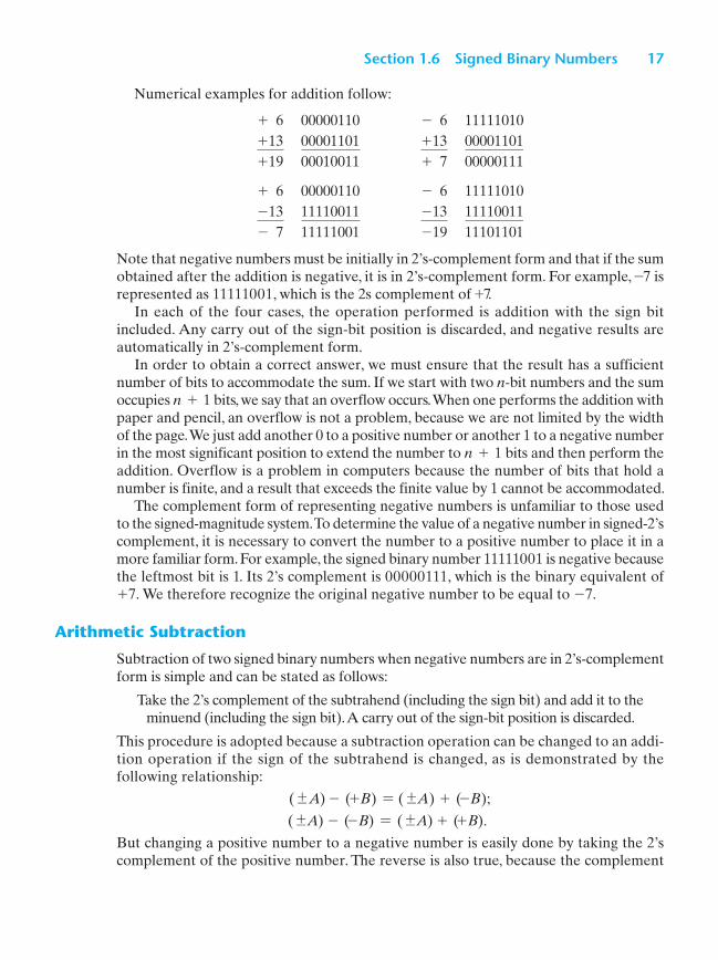
Numerical examples for addition follow:
+ 6 00000110 - 6 11111010
+13 00001101 +13 00001101
+19 00010011 + 7 00000111
+ 6 00000110 - 6 11111010
-13 11110011 -13 11110011
- 7 11111001 -19 11101101
Note that negative numbers must be initially in 2’s‐complement form and that if the sum
obtained after the addition is negative, it is in 2’s‐complement form. For example, -7 is
represented as 11111001, which is the 2s complement of +7.
In each of the four cases, the operation performed is addition with the sign bit
included. Any carry out of the sign‐bit position is discarded, and negative results are
automatically in 2’s‐complement form.
In order to obtain a correct answer, we must ensure that the result has a sufficient
number of bits to accommodate the sum. If we start with two n‐bit numbers and the sum
occupies n + 1 bits, we say that an overflow occurs. When one performs the addition with
paper and pencil, an overflow is not a problem, because we are not limited by the width
of the page. We just add another 0 to a positive number or another 1 to a negative number
in the most significant position to extend the number to n + 1 bits and then perform the
addition. Overflow is a problem in computers because the number of bits that hold a
number is finite, and a result that exceeds the finite value by 1 cannot be accommodated.
The complement form of representing negative numbers is unfamiliar to those used
to the signed‐magnitude system. To determine the value of a negative number in signed‐2’s
complement, it is necessary to convert the number to a positive number to place it in a
more familiar form. For example, the signed binary number 11111001 is negative because
the leftmost bit is 1. Its 2’s complement is 00000111, which is the binary equivalent of
+7. We therefore recognize the original negative number to be equal to -7.
Arithmetic Subtraction
Subtraction of two signed binary numbers when negative numbers are in 2’s‐complement
form is simple and can be stated as follows:
Take the 2’s complement of the subtrahend (including the sign bit) and add it to the
minuend (including the sign bit). A carry out of the sign‐bit position is discarded.
This procedure is adopted because a subtraction operation can be changed to an addi-
tion operation if the sign of the subtrahend is changed, as is demonstrated by the
following relationship:
({A) - (+B) = ({A) + (-B);
({A) - (-B) = ({A) + (+B).
But changing a positive number to a negative number is easily done by taking the 2’s
complement of the positive number. The reverse is also true, because the complement

18 Chapter 1 Digital Systems and Binary Numbers
of a negative number in complement form produces the equivalent positive number. To
see this, consider the subtraction (-6) - (-13) = +7. In binary with eight bits, this
operation is written as (11111010 - 11110011) . The subtraction is changed to addition
by taking the 2’s complement of the subtrahend (-13), giving (+13) . In binary, this is
11111010 + 00001101 = 100000111. Removing the end carry, we obtain the correct
answer: 00000111 (+7) . It is worth noting that binary numbers in the signed‐complement system are added
and subtracted by the same basic addition and subtraction rules as unsigned numbers.
Therefore, computers need only one common hardware circuit to handle both types of arithmetic . This consideration has resulted in the signed‐complement system being used
in virtually all arithmetic units of computer systems. The user or programmer must
interpret the results of such addition or subtraction differently, depending on whether
it is assumed that the numbers are signed or unsigned.
1 . 7 B I N A RY C O D E S
Digital systems use signals that have two distinct values and circuit elements that
have two stable states. There is a direct analogy among binary signals, binary circuit
elements, and binary digits. A binary number of n digits, for example, may be repre-
sented by n binary circuit elements, each having an output signal equivalent to 0 or 1.
Digital systems represent and manipulate not only binary numbers, but also many
other discrete elements of information. Any discrete element of information that is
distinct among a group of quantities can be represented with a binary code (i.e., a
pattern of 0’s and 1’s). The codes must be in binary because, in today’s technology,
only circuits that represent and manipulate patterns of 0’s and 1’s can be manufac-
tured economically for use in computers. However, it must be realized that binary
codes merely change the symbols, not the meaning of the elements of information
that they represent. If we inspect the bits of a computer at random, we will find that
most of the time they represent some type of coded information rather than binary
numbers.
An n‐bit binary code is a group of n bits that assumes up to 2n distinct combinations
of 1’s and 0’s, with each combination representing one element of the set that is being
coded. A set of four elements can be coded with two bits, with each element assigned
one of the following bit combinations: 00, 01, 10, 11. A set of eight elements requires a
three‐bit code and a set of 16 elements requires a four‐bit code. The bit combination of
an n‐bit code is determined from the count in binary from 0 to 2n - 1. Each element
must be assigned a unique binary bit combination, and no two elements can have the
same value; otherwise, the code assignment will be ambiguous.
Although the minimum number of bits required to code 2n distinct quantities is n,
there is no maximum number of bits that may be used for a binary code. For example,
the 10 decimal digits can be coded with 10 bits, and each decimal digit can be assigned
a bit combination of nine 0’s and a 1. In this particular binary code, the digit 6 is assigned
the bit combination 0001000000.

Section 1.7 Binary Codes 19
Binary-Coded Decimal Code
Although the binary number system is the most natural system for a computer because
it is readily represented in today’s electronic technology, most people are more accus-
tomed to the decimal system. One way to resolve this difference is to convert decimal
numbers to binary, perform all arithmetic calculations in binary, and then convert the
binary results back to decimal. This method requires that we store decimal numbers in
the computer so that they can be converted to binary. Since the computer can accept
only binary values, we must represent the decimal digits by means of a code that contains
1’s and 0’s. It is also possible to perform the arithmetic operations directly on decimal
numbers when they are stored in the computer in coded form.
A binary code will have some unassigned bit combinations if the number of elements
in the set is not a multiple power of 2. The 10 decimal digits form such a set. A binary
code that distinguishes among 10 elements must contain at least four bits, but 6 out of
the 16 possible combinations remain unassigned. Different binary codes can be obtained
by arranging four bits into 10 distinct combinations. The code most commonly used for
the decimal digits is the straight binary assignment listed in Table 1.4 . This scheme is
called binary‐coded decimal and is commonly referred to as BCD. Other decimal codes
are possible and a few of them are presented later in this section.
Table 1.4 gives the four‐bit code for one decimal digit. A number with k decimal
digits will require 4k bits in BCD. Decimal 396 is represented in BCD with 12 bits as
0011 1001 0110, with each group of 4 bits representing one decimal digit. A decimal
number in BCD is the same as its equivalent binary number only when the number is
between 0 and 9. A BCD number greater than 10 looks different from its equivalent
binary number, even though both contain 1’s and 0’s. Moreover, the binary combina-tions 1010 through 1111 are not used and have no meaning in BCD. Consider decimal
185 and its corresponding value in BCD and binary:
(185)10 = (0001 1000 0101)BCD = (10111001)2
Table 1.4 Binary‐Coded Decimal (BCD)
Decimal Symbol
BCD Digit
0 0000
1 0001
2 0010
3 0011
4 0100
5 0101
6 0110
7 0111
8 1000
9 1001

20 Chapter 1 Digital Systems and Binary Numbers
The BCD value has 12 bits to encode the characters of the decimal value, but the equiv-
alent binary number needs only 8 bits. It is obvious that the representation of a BCD
number needs more bits than its equivalent binary value. However, there is an advantage
in the use of decimal numbers, because computer input and output data are generated
by people who use the decimal system.
It is important to realize that BCD numbers are decimal numbers and not binary
numbers, although they use bits in their representation. The only difference between a
decimal number and BCD is that decimals are written with the symbols 0, 1, 2, c , 9
and BCD numbers use the binary code 0000, 0001, 0010, c , 1001. The decimal value
is exactly the same. Decimal 10 is represented in BCD with eight bits as 0001 0000 and
decimal 15 as 0001 0101. The corresponding binary values are 1010 and 1111 and have
only four bits.
BCD Addition
Consider the addition of two decimal digits in BCD, together with a possible carry
from a previous less significant pair of digits. Since each digit does not exceed 9, the
sum cannot be greater than 9 + 9 + 1 = 19, with the 1 being a previous carry. Sup-
pose we add the BCD digits as if they were binary numbers. Then the binary sum will
produce a result in the range from 0 to 19. In binary, this range will be from 0000 to
10011, but in BCD, it is from 0000 to 1 1001, with the first (i.e., leftmost) 1 being a
carry and the next four bits being the BCD sum. When the binary sum is equal to or
less than 1001 (without a carry), the corresponding BCD digit is correct. However,
when the binary sum is greater than or equal to 1010, the result is an invalid BCD
digit. The addition of 6 = (0110)2 to the binary sum converts it to the correct digit and
also produces a carry as required. This is because a carry in the most significant bit
position of the binary sum and a decimal carry differ by 16 - 10 = 6. Consider the
following three BCD additions:
4 0100 4 0100 8 1000
+5 +0101 +8 +1000 +9 1001
9 1001 12 1100 17 10001
+0110 +0110
10010 10111
In each case, the two BCD digits are added as if they were two binary numbers. If the
binary sum is greater than or equal to 1010, we add 0110 to obtain the correct BCD sum
and a carry. In the first example, the sum is equal to 9 and is the correct BCD sum. In
the second example, the binary sum produces an invalid BCD digit. The addition of 0110
produces the correct BCD sum, 0010 (i.e., the number 2), and a carry. In the third
example, the binary sum produces a carry. This condition occurs when the sum is greater
than or equal to 16. Although the other four bits are less than 1001, the binary sum
requires a correction because of the carry. Adding 0110, we obtain the required BCD
sum 0111 (i.e., the number 7) and a BCD carry.

Section 1.7 Binary Codes 21
The addition of two n‐digit unsigned BCD numbers follows the same procedure.
Consider the addition of 184 + 576 = 760 in BCD:
BCD 1 1
0001 1000 0100 184
+0101 0111 0110 +576
Binary sum 0111 10000 1010
Add 6 0110 0110
BCD sum 0111 0110 0000 760
The first, least significant pair of BCD digits produces a BCD digit sum of 0000 and a
carry for the next pair of digits. The second pair of BCD digits plus a previous carry
produces a digit sum of 0110 and a carry for the next pair of digits. The third pair of
digits plus a carry produces a binary sum of 0111 and does not require a correction.
Decimal Arithmetic
The representation of signed decimal numbers in BCD is similar to the representation
of signed numbers in binary. We can use either the familiar signed‐magnitude system or
the signed‐complement system. The sign of a decimal number is usually represented
with four bits to conform to the four‐bit code of the decimal digits. It is customary to
designate a plus with four 0’s and a minus with the BCD equivalent of 9, which is 1001.
The signed‐magnitude system is seldom used in computers. The signed‐complement
system can be either the 9’s or the 10’s complement, but the 10’s complement is the one
most often used. To obtain the 10’s complement of a BCD number, we first take the 9’s
complement and then add 1 to the least significant digit. The 9’s complement is calcu-
lated from the subtraction of each digit from 9.
The procedures developed for the signed‐2’s‐complement system in the previous
section also apply to the signed‐10’s‐complement system for decimal numbers. Addition
is done by summing all digits, including the sign digit, and discarding the end carry. This
operation assumes that all negative numbers are in 10’s‐complement form. Consider the
addition (+375) + (-240) = +135, done in the signed‐complement system:
0 375
+9 760
0 135
The 9 in the leftmost position of the second number represents a minus, and 9760 is
the 10’s complement of 0240. The two numbers are added and the end carry is dis-
carded to obtain +135. Of course, the decimal numbers inside the computer, including
the sign digits, must be in BCD. The addition is done with BCD digits as described
previously.
The subtraction of decimal numbers, either unsigned or in the signed‐10’s‐complement
system, is the same as in the binary case: Take the 10’s complement of the subtrahend and
add it to the minuend. Many computers have special hardware to perform arithmetic

22 Chapter 1 Digital Systems and Binary Numbers
calculations directly with decimal numbers in BCD. The user of the computer can specify
programmed instructions to perform the arithmetic operation with decimal numbers
directly, without having to convert them to binary.
Other Decimal Codes
Binary codes for decimal digits require a minimum of four bits per digit. Many different
codes can be formulated by arranging four bits into 10 distinct combinations. BCD and
three other representative codes are shown in Table 1.5 . Each code uses only 10 out of
a possible 16 bit combinations that can be arranged with four bits. The other six unused
combinations have no meaning and should be avoided.
BCD and the 2421 code are examples of weighted codes. In a weighted code, each bit
position is assigned a weighting factor in such a way that each digit can be evaluated by
adding the weights of all the 1’s in the coded combination. The BCD code has weights
of 8, 4, 2, and 1, which correspond to the power‐of‐two values of each bit. The bit assign-
ment 0110, for example, is interpreted by the weights to represent decimal 6 because
8 * 0 + 4 * 1 + 2 * 1 + 1 * 0 = 6. The bit combination 1101, when weighted by the
respective digits 2421, gives the decimal equivalent of 2 * 1 + 4 * 1 + 2 * 0 + 1 * 1 = 7.
Note that some digits can be coded in two possible ways in the 2421 code. For instance,
decimal 4 can be assigned to bit combination 0100 or 1010, since both combinations add
up to a total weight of 4.
Table 1.5 Four Different Binary Codes for the Decimal Digits
Decimal Digit
BCD 8421 2421 Excess‐3 8, 4, �2, �1
0 0000 0000 0011 0000
1 0001 0001 0100 0111
2 0010 0010 0101 0110
3 0011 0011 0110 0101
4 0100 0100 0111 0100
5 0101 1011 1000 1011
6 0110 1100 1001 1010
7 0111 1101 1010 1001
8 1000 1110 1011 1000
9 1001 1111 1100 1111
1010 0101 0000 0001
Unused 1011 0110 0001 0010
bit 1100 0111 0010 0011
combi- 1101 1000 1101 1100
nations 1110 1001 1110 1101
1111 1010 1111 1110

Section 1.7 Binary Codes 23
BCD adders add BCD values directly, digit by digit, without converting the numbers
to binary. However, it is necessary to add 6 to the result if it is greater than 9. BCD
adders require significantly more hardware and no longer have a speed advantage of
conventional binary adders [5].
The 2421 and the excess‐3 codes are examples of self‐complementing codes. Such
codes have the property that the 9’s complement of a decimal number is obtained
directly by changing 1’s to 0’s and 0’s to 1’s (i.e., by complementing each bit in the pat-
tern). For example, decimal 395 is represented in the excess‐3 code as 0110 1100 1000.
The 9’s complement of 604 is represented as 1001 0011 0111, which is obtained simply
by complementing each bit of the code (as with the 1’s complement of binary numbers).
The excess‐3 code has been used in some older computers because of its self‐
complementing property. Excess‐3 is an unweighted code in which each coded com-bination is obtained from the corresponding binary value plus 3. Note that the BCD
code is not self‐complementing.
The 8, 4, -2, -1 code is an example of assigning both positive and negative weights
to a decimal code. In this case, the bit combination 0110 is interpreted as decimal 2 and
is calculated from 8 * 0 + 4 * 1 + (-2) * 1 + (-1) * 0 = 2.
Gray Code
The output data of many physical systems are quantities that are continuous. These
data must be converted into digital form before they are applied to a digital system.
Continuous or analog information is converted into digital form by means of an ana-
log‐to‐digital converter. It is sometimes convenient to use the Gray code shown in
Table 1.6 to represent digital data that have been converted from analog data. The
advantage of the Gray code over the straight binary number sequence is that only
one bit in the code group changes in going from one number to the next. For example,
in going from 7 to 8, the Gray code changes from 0100 to 1100. Only the first bit
changes, from 0 to 1; the other three bits remain the same. By contrast, with binary
numbers the change from 7 to 8 will be from 0111 to 1000, which causes all four bits
to change values.
The Gray code is used in applications in which the normal sequence of binary numbers
generated by the hardware may produce an error or ambiguity during the transition from
one number to the next. If binary numbers are used, a change, for example, from 0111 to
1000 may produce an intermediate erroneous number 1001 if the value of the rightmost
bit takes longer to change than do the values of the other three bits. This could have seri-
ous consequences for the machine using the information. The Gray code eliminates this
problem, since only one bit changes its value during any transition between two numbers.
A typical application of the Gray code is the representation of analog data by a con-
tinuous change in the angular position of a shaft. The shaft is partitioned into segments,
and each segment is assigned a number. If adjacent segments are made to correspond
with the Gray‐code sequence, ambiguity is eliminated between the angle of the shaft
and the value encoded by the sensor.

24 Chapter 1 Digital Systems and Binary Numbers
ASCII Character Code
Many applications of digital computers require the handling not only of numbers, but
also of other characters or symbols, such as the letters of the alphabet. For instance,
consider a high‐tech company with thousands of employees. To represent the names
and other pertinent information, it is necessary to formulate a binary code for the let-
ters of the alphabet. In addition, the same binary code must represent numerals and
special characters (such as $). An alphanumeric character set is a set of elements that
includes the 10 decimal digits, the 26 letters of the alphabet, and a number of special
characters. Such a set contains between 36 and 64 elements if only capital letters are
included, or between 64 and 128 elements if both uppercase and lowercase letters are
included. In the first case, we need a binary code of six bits, and in the second, we need
a binary code of seven bits.
The standard binary code for the alphanumeric characters is the American Standard
Code for Information Interchange (ASCII), which uses seven bits to code 128 charac-
ters, as shown in Table 1.7 . The seven bits of the code are designated by b1 through b7,
with b7 the most significant bit. The letter A, for example, is represented in ASCII as
1000001 (column 100, row 0001). The ASCII code also contains 94 graphic characters
that can be printed and 34 nonprinting characters used for various control functions.
The graphic characters consist of the 26 uppercase letters (A through Z), the 26 lower-
case letters (a through z), the 10 numerals (0 through 9), and 32 special printable char-
acters, such as %, *, and $.
Table 1.6 Gray Code
Gray Code
Decimal Equivalent
0000 0
0001 1
0011 2
0010 3
0110 4
0111 5
0101 6
0100 7
1100 8
1101 9
1111 10
1110 11
1010 12
1011 13
1001 14
1000 15

Section 1.7 Binary Codes 25
Table 1.7 American Standard Code for Information Interchange (ASCII)
b7b6b5
b4b3b2b1 000 001 010 011 100 101 110 111
0000 NUL DLE SP 0 @ P ̀ p
0001 SOH DC1 ! 1 A Q a q
0010 STX DC2 “ 2 B R b r
0011 ETX DC3 # 3 C S c s
0100 EOT DC4 $ 4 D T d t
0101 ENQ NAK % 5 E U e u
0110 ACK SYN & 6 F V f v
0111 BEL ETB ‘ 7 G W g w
1000 BS CAN ( 8 H X h x
1001 HT EM ) 9 I Y i y
1010 LF SUB * : J Z j z
1011 VT ESC + ; K [ k {
1100 FF FS , < L \ l |
1101 CR GS - = M ] m }
1110 SO RS . > N ¿ n ~
1111 SI US / ? O - o DEL
Control Characters
NUL Null DLE Data‐link escape
SOH Start of heading DC1 Device control 1
STX Start of text DC2 Device control 2
ETX End of text DC3 Device control 3
EOT End of transmission DC4 Device control 4
ENQ Enquiry NAK Negative acknowledge
ACK Acknowledge SYN Synchronous idle
BEL Bell ETB End‐of‐transmission block
BS Backspace CAN Cancel
HT Horizontal tab EM End of medium
LF Line feed SUB Substitute
VT Vertical tab ESC Escape
FF Form feed FS File separator
CR Carriage return GS Group separator
SO Shift out RS Record separator
SI Shift in US Unit separator
SP Space DEL Delete
The 34 control characters are designated in the ASCII table with abbreviated names. They
are listed again below the table with their functional names. The control characters are used
for routing data and arranging the printed text into a prescribed format. There are three types
of control characters: format effectors, information separators, and communication‐control

26 Chapter 1 Digital Systems and Binary Numbers
characters. Format effectors are characters that control the layout of printing. They include
the familiar word processor and typewriter controls such as backspace (BS), horizontal tabu-
lation (HT), and carriage return (CR). Information separators are used to separate the data
into divisions such as paragraphs and pages. They include characters such as record separator
(RS) and file separator (FS). The communication‐control characters are useful during
the transmission of text between remote devices so that it can be distinguished from other
messages using the same communication channel before it and after it. Examples of
communication‐control characters are STX (start of text) and ETX (end of text), which are
used to frame a text message transmitted through a communication channel.
ASCII is a seven‐bit code, but most computers manipulate an eight‐bit quantity
as a single unit called a byte. Therefore, ASCII characters most often are stored one
per byte. The extra bit is sometimes used for other purposes, depending on the appli-
cation. For example, some printers recognize eight‐bit ASCII characters with the
most significant bit set to 0. An additional 128 eight‐bit characters with the most
significant bit set to 1 are used for other symbols, such as the Greek alphabet or italic
type font.
Error‐Detecting Code
To detect errors in data communication and processing, an eighth bit is sometimes added
to the ASCII character to indicate its parity. A parity bit is an extra bit included with a
message to make the total number of 1’s either even or odd. Consider the following two
characters and their even and odd parity:
With even parity With odd parity ASCII A = 1000001 01000001 11000001
ASCII T = 1010100 11010100 01010100
In each case, we insert an extra bit in the leftmost position of the code to produce an
even number of 1’s in the character for even parity or an odd number of 1’s in the char-
acter for odd parity. In general, one or the other parity is adopted, with even parity being
more common.
The parity bit is helpful in detecting errors during the transmission of information
from one location to another. This function is handled by generating an even parity bit
at the sending end for each character. The eight‐bit characters that include parity bits
are transmitted to their destination. The parity of each character is then checked at the
receiving end. If the parity of the received character is not even, then at least one bit has
changed value during the transmission. This method detects one, three, or any odd com-
bination of errors in each character that is transmitted. An even combination of errors,
however, goes undetected, and additional error detection codes may be needed to take
care of that possibility.
What is done after an error is detected depends on the particular application. One
possibility is to request retransmission of the message on the assumption that the error
was random and will not occur again. Thus, if the receiver detects a parity error, it sends

Section 1.8 Binary Storage and Registers 27
back the ASCII NAK (negative acknowledge) control character consisting of an even‐
parity eight bits 10010101. If no error is detected, the receiver sends back an ACK
(acknowledge) control character, namely, 00000110. The sending end will respond to an
NAK by transmitting the message again until the correct parity is received. If, after a
number of attempts, the transmission is still in error, a message can be sent to the oper-
ator to check for malfunctions in the transmission path.
1 . 8 B I N A RY S T O R A G E A N D R E G I S T E R S
The binary information in a digital computer must have a physical existence in some
medium for storing individual bits. A binary cell is a device that possesses two stable
states and is capable of storing one bit (0 or 1) of information. The input to the cell
receives excitation signals that set it to one of the two states. The output of the cell is
a physical quantity that distinguishes between the two states. The information stored
in a cell is 1 when the cell is in one stable state and 0 when the cell is in the other stable
state.
Registers
A register is a group of binary cells. A register with n cells can store any discrete quantity
of information that contains n bits. The state of a register is an n‐tuple of 1’s and 0’s, with
each bit designating the state of one cell in the register. The content of a register is a
function of the interpretation given to the information stored in it. Consider, for example,
a 16‐bit register with the following binary content:
1100001111001001
A register with 16 cells can be in one of 216 possible states. If one assumes that the con-
tent of the register represents a binary integer, then the register can store any binary
number from 0 to 216 - 1. For the particular example shown, the content of the register
is the binary equivalent of the decimal number 50,121. If one assumes instead that the
register stores alphanumeric characters of an eight‐bit code, then the content of the
register is any two meaningful characters. For the ASCII code with an even parity placed
in the eighth most significant bit position, the register contains the two characters C (the
leftmost eight bits) and I (the rightmost eight bits). If, however, one interprets the con-
tent of the register to be four decimal digits represented by a four‐bit code, then the
content of the register is a four‐digit decimal number. In the excess‐3 code, the register
holds the decimal number 9,096. The content of the register is meaningless in BCD,
because the bit combination 1100 is not assigned to any decimal digit. From this exam-
ple, it is clear that a register can store discrete elements of information and that the same
bit configuration may be interpreted differently for different types of data depending
on the application.

28 Chapter 1 Digital Systems and Binary Numbers
Register Transfer
A digital system is characterized by its registers and the components that perform data
processing. In digital systems, a register transfer operation is a basic operation that con-
sists of a transfer of binary information from one set of registers into another set of
registers. The transfer may be direct, from one register to another, or may pass through
data‐processing circuits to perform an operation. Figure 1.1 illustrates the transfer of infor-
mation among registers and demonstrates pictorially the transfer of binary information
from a keyboard into a register in the memory unit. The input unit is assumed to have a
keyboard, a control circuit, and an input register. Each time a key is struck, the control
circuit enters an equivalent eight‐bit alphanumeric character code into the input register.
We shall assume that the code used is the ASCII code with an odd‐parity bit. The informa-
tion from the input register is transferred into the eight least significant cells of a processor
register. After every transfer, the input register is cleared to enable the control to insert a
new eight‐bit code when the keyboard is struck again. Each eight‐bit character transferred
to the processor register is preceded by a shift of the previous character to the next eight
cells on its left. When a transfer of four characters is completed, the processor register is
full, and its contents are transferred into a memory register. The content stored in the
MEMORY UNIT
PROCESSOR UNIT
INPUT UNIT
J O H NMemoryRegister
8 cells 8 cells 8 cells
8 cells
8 cells
Keyboard CONTROL
01001010010011111100100011001110
ProcessorRegister
InputRegister
J
O
H
N
FIGURE 1.1 Transfer of information among registers

Section 1.8 Binary Storage and Registers 29
memory register shown in Fig. 1.1 came from the transfer of the characters “J,” “O,” “H,”
and “N” after the four appropriate keys were struck.
To process discrete quantities of information in binary form, a computer must be
provided with devices that hold the data to be processed and with circuit elements that
manipulate individual bits of information. The device most commonly used for holding data is a register. Binary variables are manipulated by means of digital logic circuits.
Figure 1.2 illustrates the process of adding two 10‐bit binary numbers. The memory unit,
which normally consists of millions of registers, is shown with only three of its registers.
The part of the processor unit shown consists of three registers—R1, R2, and R3—
together with digital logic circuits that manipulate the bits of R1 and R2 and transfer into
R3 a binary number equal to their arithmetic sum. Memory registers store information
and are incapable of processing the two operands. However, the information stored in
memory can be transferred to processor registers, and the results obtained in processor
registers can be transferred back into a memory register for storage until needed again.
The diagram shows the contents of two operands transferred from two memory registers
MEMORY UNIT
PROCESSOR UNIT
Operand 1
Operand 2
Sum
R1
R2
R3
0 0 0 0 0 0 0 0 0 0
0 0 1 1 1 0 0 0 0 1
0 0 1 1 1 0 0 0 0 1
0 0 0 1 0 0 0 0 1 0
0 0 0 1 0 0 0 0 1 0
0 1 0 0 1 0 0 0 1 1Digital logiccircuits for
binary addition
FIGURE 1.2 Example of binary information processing

30 Chapter 1 Digital Systems and Binary Numbers
into R1 and R2. The digital logic circuits produce the sum, which is transferred to register
R3. The contents of R3 can now be transferred back to one of the memory registers.
The last two examples demonstrated the information‐flow capabilities of a digital
system in a simple manner. The registers of the system are the basic elements for storing
and holding the binary information. Digital logic circuits process the binary information
stored in the registers. Digital logic circuits and registers are covered in Chapters 2
through 6. The memory unit is explained in Chapter 7 . The description of register oper-
ations at the register transfer level and the design of digital systems are covered in
Chapter 8 .
1 . 9 B I N A RY L O G I C
Binary logic deals with variables that take on two discrete values and with operations
that assume logical meaning. The two values the variables assume may be called by dif-
ferent names (true and false, yes and no, etc.), but for our purpose, it is convenient to
think in terms of bits and assign the values 1 and 0. The binary logic introduced in this
section is equivalent to an algebra called Boolean algebra. The formal presentation of
Boolean algebra is covered in more detail in Chapter 2 . The purpose of this section is
to introduce Boolean algebra in a heuristic manner and relate it to digital logic circuits
and binary signals.
Definition of Binary Logic
Binary logic consists of binary variables and a set of logical operations. The variables are
designated by letters of the alphabet, such as A, B, C, x, y, z, etc., with each variable hav-
ing two and only two distinct possible values: 1 and 0. There are three basic logical oper-
ations: AND, OR, and NOT. Each operation produces a binary result, denoted by z.
1. AND: This operation is represented by a dot or by the absence of an operator. For
example, x # y = z or xy = z is read “x AND y is equal to z.” The logical operation
AND is interpreted to mean that z = 1 if and only if x = 1 and y = 1; otherwise
z = 0. (Remember that x, y, and z are binary variables and can be equal either to
1 or 0, and nothing else.) The result of the operation x # y is z.
2. OR: This operation is represented by a plus sign. For example, x + y = z is read
“x OR y is equal to z,” meaning that z = 1 if x = 1 or if y = 1 or if both x = 1
and y = 1. If both x = 0 and y = 0, then z = 0.
3. NOT: This operation is represented by a prime (sometimes by an overbar). For
example, x� = z (or x = z ) is read “not x is equal to z,” meaning that z is what x
is not. In other words, if x = 1, then z = 0, but if x = 0, then z = 1. The NOT
operation is also referred to as the complement operation, since it changes a 1 to
0 and a 0 to 1, i.e., the result of complementing 1 is 0, and vice versa.
Binary logic resembles binary arithmetic, and the operations AND and OR have
similarities to multiplication and addition, respectively. In fact, the symbols used for

Section 1.9 Binary Logic 31
AND and OR are the same as those used for multiplication and addition. However,
binary logic should not be confused with binary arithmetic. One should realize that an
arithmetic variable designates a number that may consist of many digits. A logic vari-
able is always either 1 or 0. For example, in binary arithmetic, we have 1 + 1 = 10 (read
“one plus one is equal to 2”), whereas in binary logic, we have 1 + 1 = 1 (read “one
OR one is equal to one”).
For each combination of the values of x and y, there is a value of z specified by the
definition of the logical operation. Definitions of logical operations may be listed in a
compact form called truth tables. A truth table is a table of all possible combinations of
the variables, showing the relation between the values that the variables may take and
the result of the operation. The truth tables for the operations AND and OR with vari-
ables x and y are obtained by listing all possible values that the variables may have when
combined in pairs. For each combination, the result of the operation is then listed in a
separate row. The truth tables for AND, OR, and NOT are given in Table 1.8 . These
tables clearly demonstrate the definition of the operations.
Logic Gates
Logic gates are electronic circuits that operate on one or more input signals to pro-
duce an output signal. Electrical signals such as voltages or currents exist as analog
signals having values over a given continuous range, say, 0 to 3 V, but in a digital
system these voltages are interpreted to be either of two recognizable values, 0 or 1.
Voltage‐operated logic circuits respond to two separate voltage levels that represent a
binary variable equal to logic 1 or logic 0. For example, a particular digital system may
define logic 0 as a signal equal to 0 V and logic 1 as a signal equal to 3 V. In practice,
each voltage level has an acceptable range, as shown in Fig. 1.3 . The input terminals of
digital circuits accept binary signals within the allowable range and respond at the
output terminals with binary signals that fall within the specified range. The intermedi-
ate region between the allowed regions is crossed only during a state transition. Any
desired information for computing or control can be operated on by passing binary
signals through various combinations of logic gates, with each signal representing a
particular binary variable. When the physical signal is in a particular range it is inter-
preted to be either a 0 or a 1.
Table 1.8 Truth Tables of Logical Operations
AND OR NOT
x y x # y x y x + y x x�
0 0 0 0 0 0 0 1
0 1 0 0 1 1 1 0
1 0 0 1 0 1
1 1 1 1 1 1
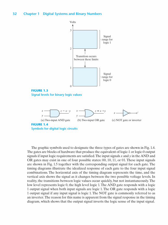
32 Chapter 1 Digital Systems and Binary Numbers
The graphic symbols used to designate the three types of gates are shown in Fig. 1.4 .
The gates are blocks of hardware that produce the equivalent of logic‐1 or logic‐0 output
signals if input logic requirements are satisfied. The input signals x and y in the AND and
OR gates may exist in one of four possible states: 00, 10, 11, or 01. These input signals
are shown in Fig. 1.5 together with the corresponding output signal for each gate. The
timing diagrams illustrate the idealized response of each gate to the four input signal
combinations. The horizontal axis of the timing diagram represents the time, and the
vertical axis shows the signal as it changes between the two possible voltage levels. In
reality, the transitions between logic values occur quickly, but not instantaneously. The
low level represents logic 0, the high level logic 1. The AND gate responds with a logic
1 output signal when both input signals are logic 1. The OR gate responds with a logic
1 output signal if any input signal is logic 1. The NOT gate is commonly referred to as
an inverter. The reason for this name is apparent from the signal response in the timing
diagram, which shows that the output signal inverts the logic sense of the input signal.
Volts
Signalrange for
logic 1
Signalrange for
logic 0
0
1
2
3
Transition occursbetween these limits
FIGURE 1.3 Signal levels for binary logic values
x x�
(c) NOT gate or inverter(a) Two-input AND gate
x z � x � y
y
(b) Two-input OR gate
z � x �yx
y
FIGURE 1.4 Symbols for digital logic circuits

Problems 33
AND and OR gates may have more than two inputs. An AND gate with three inputs
and an OR gate with four inputs are shown in Fig. 1.6 . The three‐input AND gate
responds with logic 1 output if all three inputs are logic 1. The output produces logic 0
if any input is logic 0. The four‐input OR gate responds with logic 1 if any input is logic
1; its output becomes logic 0 only when all inputs are logic 0.
P R O B L E M S
(Answers to problems marked with * appear at the end of the text.)
1.1 List the octal and hexadecimal numbers from 16 to 32. Using A and B for the last two
digits, list the numbers from 8 to 28 in base 12.
1.2* What is the exact number of bytes in a system that contains (a) 32K bytes, (b) 64M bytes,
and (c) 6.4G bytes?
1.3 Convert the following numbers with the indicated bases to decimal:
(a) * (4310) 5 (b) * (198) 12
(c) (435) 8 (d) (345) 6
1.4 What is the largest binary number that can be expressed with 16 bits? What are the equiv-
alent decimal and hexadecimal numbers?
1.5* Determine the base of the numbers in each case for the following operations to be correct:
(a) 14/2 = 5 (b) 54/4 = 13 (c) 24 + 17 = 40.
1.6* The solutions to the quadratic equation x 2 - 11x + 22 = 0 are x = 3 and x = 6. What is the
base of the numbers?
x
y
AND: x � y
OR: x � y
NOT: x�
0 0 01 1
0 1 00 1
0 0 00 1
0 1 01 1
1 1 10 0
FIGURE 1.5 Input–output signals for gates
ABC
F � ABC G � A � B � C � DABCD
(a) Three-input AND gate (b) Four-input OR gate
FIGURE 1.6 Gates with multiple inputs

34 Chapter 1 Digital Systems and Binary Numbers
1.7* Convert the hexadecimal number 64CD to binary, and then convert it from binary to octal.
1.8 Convert the decimal number 431 to binary in two ways: (a) convert directly to binary;
(b) convert first to hexadecimal and then from hexadecimal to binary. Which method is faster?
1.9 Express the following numbers in decimal:
(a) * (10110.0101) 2 (b) * (16.5) 16
(c) * (26.24) 8 (d) (DADA.B) 16
(e) (1010.1101) 2
1.10 Convert the following binary numbers to hexadecimal and to decimal: (a) 1.10010,
(b) 110.010. Explain why the decimal answer in (b) is 4 times that in (a).
1.11 Perform the following division in binary: 111011 ÷ 101.
1.12* Add and multiply the following numbers without converting them to decimal.
(a) Binary numbers 1011 and 101.
(b) Hexadecimal numbers 2E and 34.
1.13 Do the following conversion problems:
(a) Convert decimal 27.315 to binary.
(b) Calculate the binary equivalent of 2/3 out to eight places. Then convert from binary to
decimal. How close is the result to 2/3?
(c) Convert the binary result in (b) into hexadecimal. Then convert the result to decimal.
Is the answer the same?
1.14 Obtain the 1’s and 2’s complements of the following binary numbers:
(a) 00010000 (b) 00000000
(c) 11011010 (d) 10101010
(e) 10000101 (f) 11111111.
1.15 Find the 9’s and the 10’s complement of the following decimal numbers:
(a) 25,478,036 (b) 63, 325, 600
(c) 25,000,000 (d) 00,000,000.
1.16 (a) Find the 16’s complement of C3DF.
(b) Convert C3DF to binary.
(c) Find the 2’s complement of the result in (b).
(d) Convert the answer in (c) to hexadecimal and compare with the answer in (a).
1.17 Perform subtraction on the given unsigned numbers using the 10’s complement of the
subtrahend. Where the result should be negative, find its 10’s complement and affix a minus
sign. Verify your answers.
(a) 4,637 - 2,579 (b) 125 - 1,800
(c) 2,043 - 4,361 (d) 1,631 - 745
1.18 Perform subtraction on the given unsigned binary numbers using the 2’s complement of the
subtrahend. Where the result should be negative, find its 2’s complement and affix a minus sign.
(a) 10011 - 10010 (b) 100010 - 100110
(c) 1001 - 110101 (d) 101000 - 10101
1.19* The following decimal numbers are shown in sign‐magnitude form: +9,286 and +801.
Convert them to signed-10’s‐complement form and perform the following operations
(note that the sum is +10,627 and requires five digits and a sign).
(a) (+9,286) + (+801) (b) (+9,286) + (-801)
(c) (-9,286) + (+801) (d) (-9,286) + (-801)

Problems 35
1.20 Convert decimal +49 and +29 to binary, using the signed‐2’s‐complement representation
and enough digits to accommodate the numbers. Then perform the binary equivalent of
(+29) + (-49), (-29) + (+49), and (-29) + (-49). Convert the answers back to decimal and
verify that they are correct.
1.21 If the numbers (+9,742) 10 and (+641) 10 are in signed magnitude format, their sum is (+10,383) 10
and requires five digits and a sign. Convert the numbers to signed-10’s‐complement form and
find the following sums:
(a) (+9,742) + (+641) (b) (+9,742) + (-641)
(c) (-9,742) + (+641) (d) (-9,742) + (-641)
1.22 Convert decimal 6,514 to both BCD and ASCII codes. For ASCII, an even parity bit is to
be appended at the left.
1.23 Represent the unsigned decimal numbers 791 and 658 in BCD, and then show the steps
necessary to form their sum.
1.24 Formulate a weighted binary code for the decimal digits, using the following weights:
(a) * 6, 3, 1, 1
(b) 6, 4, 2, 1
1.25 Represent the decimal number 6,248 in (a) BCD, (b) excess‐3 code, (c) 2421 code, and
(d) a 6311 code.
1.26 Find the 9’s complement of decimal 6,248 and express it in 2421 code. Show that the result
is the 1’s complement of the answer to (c) in CR_PROBlem 1.25. This demonstrates that
the 2421 code is self‐complementing.
1.27 Assign a binary code in some orderly manner to the 52 playing cards. Use the minimum
number of bits.
1.28 Write the expression “G. Boole” in ASCII, using an eight‐bit code. Include the period and
the space. Treat the leftmost bit of each character as a parity bit. Each eight‐bit code should
have odd parity. (George Boole was a 19th‐century mathematician. Boolean algebra,
introduced in the next chapter, bears his name.)
1.29* Decode the following ASCII code:
1010011 1110100 1100101 1110110 1100101 0100000 1001010 1101111 1100010 1110011.
1.30 The following is a string of ASCII characters whose bit patterns have been converted into
hexadecimal for compactness: 73 F4 E5 76 E5 4A EF 62 73. Of the eight bits in each pair
of digits, the leftmost is a parity bit. The remaining bits are the ASCII code.
(a) Convert the string to bit form and decode the ASCII.
(b) Determine the parity used: odd or even?
1.31* How many printing characters are there in ASCII? How many of them are special char-
acters (not letters or numerals)?
1.32* What bit must be complemented to change an ASCII letter from capital to lowercase and
vice versa?
1.33* The state of a 12‐bit register is 100010010111. What is its content if it represents
(a) Three decimal digits in BCD?
(b) Three decimal digits in the excess‐3 code?
(c) Three decimal digits in the 84‐2‐1 code?
(d) A binary number?

36 Chapter 1 Digital Systems and Binary Numbers
1.34 List the ASCII code for the 10 decimal digits with an even parity bit in the leftmost
position.
1.35 By means of a timing diagram similar to Fig. 1.5 , show the signals of the outputs f and g in
Fig. P1.35 as functions of the three inputs a, b, and c. Use all eight possible combinations
of a, b, and c.
f
g
a b c
FIGURE P1.35
f
g
a b
FIGURE P1.36
1.36 By means of a timing diagram similar to Fig. 1.5 , show the signals of the outputs f and g in
Fig. P1.36 as functions of the two inputs a and b. Use all four possible combinations of a
and b.
R E F E R E N C E S
1. C avanagh, J. J. 1984. Digital Computer Arithmetic. New York: McGraw‐Hill.
2. M ano, M. M. 1988. Computer Engineering: Hardware Design. Englewood Cliffs, NJ:
Prentice‐Hall.
3. N elson, V. P., H. T. N agle, J. D. I rwin, and B. D. C arroll . 1997. Digital Logic Circuit Analysis and Design. Upper Saddle River, NJ: Prentice Hall.
4. S chmid, H. 1974. Decimal Computation. New York: John Wiley.
5. Katz, R. H. and Borriello, G. 2004. Contemporary Logic Design, 2nd ed. Upper Saddle
River, NJ: Prentice‐Hall.

Web Search Topics 37
W E B S E A R C H T O P I C S
BCD code
ASCII
Storage register
Binary logic
BCD addition
Binary codes
Binary numbers
Excess‐3 code

38
Chapter 2
Boolean Algebra and Logic Gates
2 . 1 I N T R O D U C T I O N
Because binary logic is used in all of today’s digital computers and devices, the cost of
the circuits that implement it is an important factor addressed by designers—be they
computer engineers, electrical engineers, or computer scientists. Finding simpler and
cheaper, but equivalent, realizations of a circuit can reap huge payoffs in reducing the
overall cost of the design. Mathematical methods that simplify circuits rely primarily on
Boolean algebra. Therefore, this chapter provides a basic vocabulary and a brief founda-
tion in Boolean algebra that will enable you to optimize simple circuits and to under-
stand the purpose of algorithms used by software tools to optimize complex circuits
involving millions of logic gates.
2 . 2 B A S I C D E F I N I T I O N S
Boolean algebra, like any other deductive mathematical system, may be defined with a
set of elements, a set of operators, and a number of unproved axioms or postulates. A set of elements is any collection of objects, usually having a common property. If S is a set,
and x and y are certain objects, then the notation x H S means that x is a member of the
set S and y x S means that y is not an element of S. A set with a denumerable number
of elements is specified by braces: A = {1, 2, 3, 4} indicates that the elements of set A
are the numbers 1, 2, 3, and 4. A binary operator defined on a set S of elements is a rule
that assigns, to each pair of elements from S, a unique element from S. As an example,
consider the relation a*b = c. We say that * is a binary operator if it specifies a rule
for finding c from the pair (a, b) and also if a, b, c H S. However, * is not a binary operator
if a, b H S, and if c x S.

Section 2.2 Basic Definitions 39
The postulates of a mathematical system form the basic assumptions from which it
is possible to deduce the rules, theorems, and properties of the system. The most com-
mon postulates used to formulate various algebraic structures are as follows:
1. Closure. A set S is closed with respect to a binary operator if, for every pair of
elements of S, the binary operator specifies a rule for obtaining a unique element
of S. For example, the set of natural numbers N = {1, 2, 3, 4, c} is closed with
respect to the binary operator + by the rules of arithmetic addition, since, for any
a, b H N, there is a unique c H N such that a + b = c. The set of natural numbers
is not closed with respect to the binary operator - by the rules of arithmetic
subtraction, because 2 - 3 = -1 and 2, 3 H N, but (-1) x N.
2. Associative law. A binary operator * on a set S is said to be associative whenever
(x*y)*z = x* (y*z) for all x, y, z, H S
3. Commutative law. A binary operator * on a set S is said to be commutative when-
ever
x*y = y*x for all x, y H S
4. Identity element. A set S is said to have an identity element with respect to a binary
operation * on S if there exists an element e H S with the property that
e*x = x*e = x for every x H S
Example: The element 0 is an identity element with respect to the binary operator
+ on the set of integers I = {c , -3, -2, -1, 0, 1, 2, 3,c}, since
x + 0 = 0 + x = x for any x H I
The set of natural numbers, N, has no identity element, since 0 is excluded from the set.
5. Inverse. A set S having the identity element e with respect to a binary operator *
is said to have an inverse whenever, for every x H S, there exists an element y H S
such that
x *y = e
Example: In the set of integers, I, and the operator + , with e = 0, the inverse of
an element a is (-a), since a + (-a) = 0.
6. Distributive law. If * and # are two binary operators on a set S, * is said to be dis-
tributive over # whenever
x* (y # z) = (x*y) # (x*z)
A field is an example of an algebraic structure. A field is a set of elements, together with
two binary operators, each having properties 1 through 5 and both operators combining
to give property 6. The set of real numbers, together with the binary operators + and # ,

40 Chapter 2 Boolean Algebra and Logic Gates
forms the field of real numbers. The field of real numbers is the basis for arithmetic and
ordinary algebra. The operators and postulates have the following meanings:
The binary operator + defines addition.
The additive identity is 0.
The additive inverse defines subtraction.
The binary operator # defines multiplication.
The multiplicative identity is 1.
For a � 0, the multiplicative inverse of a = 1>a defines division (i.e., a # 1>a = 1 ).
The only distributive law applicable is that of # over + :
a # (b + c) = (a # b) + (a # c)
2 . 3 A X I O M AT I C D E F I N I T I O N O F B O O L E A N A L G E B R A
In 1854, George Boole developed an algebraic system now called Boolean algebra. In
1938, Claude E. Shannon introduced a two‐valued Boolean algebra called switching algebra that represented the properties of bistable electrical switching circuits. For the
formal definition of Boolean algebra, we shall employ the postulates formulated by
E. V. Huntington in 1904.
Boolean algebra is an algebraic structure defined by a set of elements, B, together
with two binary operators, + and # , provided that the following (Huntington) postulates
are satisfied:
1. (a) The structure is closed with respect to the operator + .
(b) The structure is closed with respect to the operator # .
2. (a) The element 0 is an identity element with respect to + ; that is, x + 0 =
0 + x = x .
(b) The element 1 is an identity element with respect to # ; that is, x # 1 = 1 # x = x.
3. (a) The structure is commutative with respect to + ; that is, x + y = y + x .
(b) The structure is commutative with respect to # ; that is, x # y = y # x.
4. (a) The operator # is distributive over + ; that is, x # (y + z) = (x # y) + (x # z).
(b) The operator + is distributive over # ; that is, x + (y # z) = (x + y) # (x + z).
5. For every element x H B, there exists an element x� H B (called the complement of x)
such that (a) x + x� = 1 and (b) x # x� = 0.
6. There exist at least two elements x, y H B such that x � y.
Comparing Boolean algebra with arithmetic and ordinary algebra (the field of real
numbers), we note the following differences:
1. Huntington postulates do not include the associative law. However, this law holds for
Boolean algebra and can be derived (for both operators) from the other postulates.
2. The distributive law of + over # (i.e., x + (y # z) = (x + y) # (x + z) ) is valid for
Boolean algebra, but not for ordinary algebra.

Section 2.3 Axiomatic Definition of Boolean Algebra 41
3. Boolean algebra does not have additive or multiplicative inverses; therefore, there
are no subtraction or division operations.
4. Postulate 5 defines an operator called the complement that is not available in
ordinary algebra.
5. Ordinary algebra deals with the real numbers, which constitute an infinite set of
elements. Boolean algebra deals with the as yet undefined set of elements, B, but
in the two‐valued Boolean algebra defined next (and of interest in our subse-
quent use of that algebra), B is defined as a set with only two elements, 0 and 1.
Boolean algebra resembles ordinary algebra in some respects. The choice of the
symbols + and # is intentional, to facilitate Boolean algebraic manipulations by persons
already familiar with ordinary algebra. Although one can use some knowledge from
ordinary algebra to deal with Boolean algebra, the beginner must be careful not to
substitute the rules of ordinary algebra where they are not applicable.
It is important to distinguish between the elements of the set of an algebraic structure
and the variables of an algebraic system. For example, the elements of the field of real
numbers are numbers, whereas variables such as a, b, c, etc., used in ordinary algebra,
are symbols that stand for real numbers. Similarly, in Boolean algebra, one defines the
elements of the set B, and variables such as x, y, and z are merely symbols that represent the elements. At this point, it is important to realize that, in order to have a Boolean
algebra, one must show that
1. the elements of the set B,
2. the rules of operation for the two binary operators, and
3. the set of elements, B, together with the two operators, satisfy the six Huntington
postulates.
One can formulate many Boolean algebras, depending on the choice of elements of
B and the rules of operation. In our subsequent work, we deal only with a two‐valued Boolean algebra (i.e., a Boolean algebra with only two elements). Two‐valued Boolean
algebra has applications in set theory (the algebra of classes) and in propositional logic.
Our interest here is in the application of Boolean algebra to gate‐type circuits commonly
used in digital devices and computers.
Two‐Valued Boolean Algebra
A two‐valued Boolean algebra is defined on a set of two elements, B = {0, 1}, with rules
for the two binary operators + and # as shown in the following operator tables (the rule
for the complement operator is for verification of postulate 5):
x y x # y x y x � y x x�
0 0 0 0 0 0 0 1 0 1 0 0 1 1 1 0 1 0 0 1 0 1 1 1 1 1 1 1

42 Chapter 2 Boolean Algebra and Logic Gates
These rules are exactly the same as the AND, OR, and NOT operations, respectively,
defined in Table 1.8. We must now show that the Huntington postulates are valid for the
set B = {0, 1} and the two binary operators + and # .
1. That the structure is closed with respect to the two operators is obvious from the
tables, since the result of each operation is either 1 or 0 and 1, 0 H B.
2. From the tables, we see that
(a) 0 + 0 = 0 0 + 1 = 1 + 0 = 1;
(b) 1 # 1 = 1 1 # 0 = 0 # 1 = 0.
This establishes the two identity elements, 0 for + and 1 for # , as defined by
postulate 2.
3. The commutative laws are obvious from the symmetry of the binary operator tables.
4. (a) The distributive law x # (y + z) = (x # y) + (x # z) can be shown to hold from
the operator tables by forming a truth table of all possible values of x, y, and z. For
each combination, we derive x # (y + z) and show that the value is the same as the
value of (x # y) + (x # z):
x y z y � z x # (y �z) x # y x # z (x # y) �(x # z)
0 0 0 0 0 0 0 0
0 0 1 1 0 0 0 0
0 1 0 1 0 0 0 0
0 1 1 1 0 0 0 0
1 0 0 0 0 0 0 0
1 0 1 1 1 0 1 1
1 1 0 1 1 1 0 1
1 1 1 1 1 1 1 1
(b) The distributive law of + over # can be shown to hold by means of a truth table
similar to the one in part (a).
5. From the complement table, it is easily shown that
(a) x + x � = 1, since 0 + 0� = 0 + 1 = 1 and 1 + 1� = 1 + 0 = 1.
(b) x # x� = 0, since 0 # 0� = 0 # 1 = 0 and 1 # 1� = 1 # 0 = 0.
Thus, postulate 1 is verified.
6. Postulate 6 is satisfied because the two‐valued Boolean algebra has two elements,
1 and 0, with 1 � 0.
We have just established a two‐valued Boolean algebra having a set of two elements,
1 and 0, two binary operators with rules equivalent to the AND and OR operations, and
a complement operator equivalent to the NOT operator. Thus, Boolean algebra has been
defined in a formal mathematical manner and has been shown to be equivalent to the
binary logic presented heuristically in Section 1.9. The heuristic presentation is helpful
in understanding the application of Boolean algebra to gate‐type circuits. The formal

Section 2.4 Basic Theorems and Properties of Boolean Algebra 43
presentation is necessary for developing the theorems and properties of the algebraic
system. The two‐valued Boolean algebra defined in this section is also called “switching
algebra” by engineers. To emphasize the similarities between two‐valued Boolean alge-
bra and other binary systems, that algebra was called “binary logic” in Section 1.9. From
here on, we shall drop the adjective “two‐valued” from Boolean algebra in subsequent
discussions.
2 . 4 B A S I C T H E O R E M S A N D P R O P E R T I E S O F B O O L E A N A L G E B R A
Duality
In Section 2.3, the Huntington postulates were listed in pairs and designated by part
(a) and part (b). One part may be obtained from the other if the binary operators and
the identity elements are interchanged. This important property of Boolean algebra is
called the duality principle and states that every algebraic expression deducible from
the postulates of Boolean algebra remains valid if the operators and identity elements
are interchanged. In a two‐valued Boolean algebra, the identity elements and the ele-
ments of the set B are the same: 1 and 0. The duality principle has many applications. If
the dual of an algebraic expression is desired, we simply interchange OR and AND
operators and replace 1’s by 0’s and 0’s by 1’s.
Basic Theorems
Table 2.1 lists six theorems of Boolean algebra and four of its postulates. The notation
is simplified by omitting the binary operator whenever doing so does not lead to
confusion. The theorems and postulates listed are the most basic relationships in Boolean
Table 2.1 Postulates and Theorems of Boolean Algebra
Postulate 2 (a) x + 0 = x (b) x # 1 = x
Postulate 5 (a) x + x � = 1 (b) x # x� = 0
Theorem 1 (a) x + x = x (b) x # x = x
Theorem 2 (a) x + 1 = 1 (b) x # 0 = 0
Theorem 3, involution (x �)� = x
Postulate 3, commutative (a) x + y = y + x (b) xy = yx
Theorem 4, associative (a) x + (y + z) = (x + y) + z (b) x(yz) = (xy)z
Postulate 4, distributive (a) x(y + z) = xy + xz (b) x + yz = (x + y)(x + z)
Theorem 5, DeMorgan (a) (x + y)� = x �y� (b) (xy)� = x � + y�
Theorem 6, absorption (a) x + xy = x (b) x(x + y) = x

44 Chapter 2 Boolean Algebra and Logic Gates
algebra. The theorems, like the postulates, are listed in pairs; each relation is the dual of
the one paired with it. The postulates are basic axioms of the algebraic structure and
need no proof. The theorems must be proven from the postulates. Proofs of the theorems
with one variable are presented next. At the right is listed the number of the postulate
which justifies that particular step of the proof.
THEOREM 1(a): x + x = x.
Statement Justification
x + x = (x + x) # 1 postulate 2(b)
= (x + x)(x + x�) 5(a)
= x + xx� 4(b)
= x + 0 5(b)
= x 2(a)
THEOREM 1(b): x # x = x.
Statement Justification
x # x = xx + 0 postulate 2(a)
= xx + xx� 5(b)
= x(x + x�) 4(a)
= x # 1 5(a)
= x 2(b)
Note that theorem 1(b) is the dual of theorem 1(a) and that each step of the proof
in part (b) is the dual of its counterpart in part (a). Any dual theorem can be similarly
derived from the proof of its corresponding theorem.
THEOREM 2(a): x + 1 = 1.
Statement Justifi cation
x + 1 = 1 # (x + 1) postulate 2(b)
= (x + x�)(x + 1) 5(a)
= x + x� # 1 4(b)
= x + x� 2(b)
= 1 5(a)
THEOREM 2(b): x # 0 = 0 by duality.
THEOREM 3: (x�)� = x. From postulate 5, we have x + x� = 1 and x # x� = 0, which
together define the complement of x. The complement of x� is x and is also (x�)�.

Section 2.4 Basic Theorems and Properties of Boolean Algebra 45
Therefore, since the complement is unique, we have (x�)� = x. The theorems involv-
ing two or three variables may be proven algebraically from the postulates and the
theorems that have already been proven. Take, for example, the absorption theorem:
THEOREM 6(a): x + xy = x.
Statement Justifi cation
x + xy = x # 1 + xy postulate 2(b)
= x(1 + y) 4(a)
= x(y + 1) 3(a)
= x # 1 2(a)
= x 2(b)
THEOREM 6(b): x(x + y) = x by duality.
The theorems of Boolean algebra can be proven by means of truth tables. In truth
tables, both sides of the relation are checked to see whether they yield identical results
for all possible combinations of the variables involved. The following truth table verifies
the first absorption theorem:
x y xy x � xy
0 0 0 0
0 1 0 0
1 0 0 1
1 1 1 1
The algebraic proofs of the associative law and DeMorgan’s theorem are long and will
not be shown here. However, their validity is easily shown with truth tables. For example,
the truth table for the first DeMorgan’s theorem, (x + y)� = x�y�, is as follows:
x y x � y (x � y)� x� y� x�y�
0 0 0 1 1 1 1
0 1 1 0 1 0 0
1 0 1 0 0 1 0
1 1 1 0 0 0 0
Operator Precedence
The operator precedence for evaluating Boolean expressions is (1) parentheses,
(2) NOT, (3) AND, and (4) OR. In other words, expressions inside parentheses must be
evaluated before all other operations. The next operation that holds precedence is the
complement, and then follows the AND and, finally, the OR. As an example, consider
the truth table for one of DeMorgan’s theorems. The left side of the expression is
(x + y)�. Therefore, the expression inside the parentheses is evaluated first and the

46 Chapter 2 Boolean Algebra and Logic Gates
Table 2.2 Truth Tables for F1 and F2
x y z F1 F2
0 0 0 0 0
0 0 1 1 1
0 1 0 0 0
0 1 1 0 1
1 0 0 1 1
1 0 1 1 1
1 1 0 1 0
1 1 1 1 0
result then complemented. The right side of the expression is x�y�, so the complement
of x and the complement of y are both evaluated first and the result is then ANDed.
Note that in ordinary arithmetic, the same precedence holds (except for the comple-
ment) when multiplication and addition are replaced by AND and OR, respectively.
2 . 5 B O O L E A N F U N C T I O N S
Boolean algebra is an algebra that deals with binary variables and logic operations. A
Boolean function described by an algebraic expression consists of binary variables, the
constants 0 and 1, and the logic operation symbols. For a given value of the binary variables,
the function can be equal to either 1 or 0. As an example, consider the Boolean function
F1 = x + y�z
The function F1 is equal to 1 if x is equal to 1 or if both y� and z are equal to 1. F1 is equal
to 0 otherwise. The complement operation dictates that when y� = 1, y = 0. Therefore,
F1 = 1 if x = 1 or if y = 0 and z = 1. A Boolean function expresses the logical rela-
tionship between binary variables and is evaluated by determining the binary value of
the expression for all possible values of the variables.
A Boolean function can be represented in a truth table. The number of rows in the
truth table is 2n, where n is the number of variables in the function. The binary combina-
tions for the truth table are obtained from the binary numbers by counting from 0
through 2n - 1. Table 2.2 shows the truth table for the function F1. There are eight pos-
sible binary combinations for assigning bits to the three variables x, y, and z. The column
labeled F1 contains either 0 or 1 for each of these combinations. The table shows that
the function is equal to 1 when x = 1 or when yz = 01 and is equal to 0 otherwise.
A Boolean function can be transformed from an algebraic expression into a circuit
diagram composed of logic gates connected in a particular structure. The logic‐circuit
diagram (also called a schematic) for F1 is shown in Fig. 2.1 . There is an inverter for input y to generate its complement. There is an AND gate for the term y�z and an OR gate

Section 2.5 Boolean Functions 47
that combines x with y�z. In logic‐circuit diagrams, the variables of the function are taken
as the inputs of the circuit and the binary variable F1 is taken as the output of the circuit.
The schematic expresses the relationship between the output of the circuit and its inputs.
Rather than listing each combination of inputs and outputs, it indicates how to compute
the logic value of each output from the logic values of the inputs. There is only one way that a Boolean function can be represented in a truth table.
However, when the function is in algebraic form, it can be expressed in a variety of ways,
all of which have equivalent logic. The particular expression used to represent the function
will dictate the interconnection of gates in the logic‐circuit diagram. Conversely, the inter-
connection of gates will dictate the logic expression. Here is a key fact that motivates our
use of Boolean algebra: By manipulating a Boolean expression according to the rules of
Boolean algebra, it is sometimes possible to obtain a simpler expression for the same
function and thus reduce the number of gates in the circuit and the number of inputs to
the gate. Designers are motivated to reduce the complexity and number of gates because
their effort can significantly reduce the cost of a circuit. Consider, for example, the fol-
lowing Boolean function:
F2 = x�y�z + x�yz + xy�
A schematic of an implementation of this function with logic gates is shown in
Fig. 2.2 (a). Input variables x and y are complemented with inverters to obtain x� and
y�. The three terms in the expression are implemented with three AND gates. The
OR gate forms the logical OR of the three terms. The truth table for F2 is listed in
Table 2.2 . The function is equal to 1 when xyz = 001 or 011 or when xy = 10 (irre-
spective of the value of z) and is equal to 0 otherwise. This set of conditions produces
four 1’s and four 0’s for F2. Now consider the possible simplification of the function by applying some of the
identities of Boolean algebra:
F2 = x�y�z + x�yz + xy� = x�z(y� + y) + xy� = x�z + xy�
The function is reduced to only two terms and can be implemented with gates as shown
in Fig. 2.2 (b). It is obvious that the circuit in (b) is simpler than the one in (a), yet both
implement the same function. By means of a truth table, it is possible to verify that the
two expressions are equivalent. The simplified expression is equal to 1 when xz = 01 or
when xy = 10. This produces the same four 1’s in the truth table. Since both expressions
F1x
yz
FIGURE 2.1 Gate implementation of F1 � x � y�z

48 Chapter 2 Boolean Algebra and Logic Gates
produce the same truth table, they are equivalent. Therefore, the two circuits have the
same outputs for all possible binary combinations of inputs of the three variables. Each
circuit implements the same identical function, but the one with fewer gates and fewer
inputs to gates is preferable because it requires fewer wires and components. In general,
there are many equivalent representations of a logic function. Finding the most eco-
nomic representation of the logic is an important design task.
Algebraic Manipulation
When a Boolean expression is implemented with logic gates, each term requires a gate
and each variable within the term designates an input to the gate. We define a literal to
be a single variable within a term, in complemented or uncomplemented form. The
function of Fig. 2.2 (a) has three terms and eight literals, and the one in Fig. 2.2 (b) has
two terms and four literals. By reducing the number of terms, the number of literals, or
both in a Boolean expression, it is often possible to obtain a simpler circuit. The manip-
ulation of Boolean algebra consists mostly of reducing an expression for the purpose of
obtaining a simpler circuit. Functions of up to five variables can be simplified by the
map method described in the next chapter. For complex Boolean functions and many
(a) F2 � x�y�z � x�yz � xy�
(b) F2 � xy� � x�z
x
y
zF2
x
y
z
F2
FIGURE 2.2 Implementation of Boolean function F2 with gates

Section 2.5 Boolean Functions 49
different outputs, designers of digital circuits use computer minimization programs that
are capable of producing optimal circuits with millions of logic gates. The concepts intro-
duced in this chapter provide the framework for those tools. The only manual method
available is a cut‐and‐try procedure employing the basic relations and other manipulation
techniques that become familiar with use, but remain, nevertheless, subject to human
error. The examples that follow illustrate the algebraic manipulation of Boolean algebra
to acquaint the reader with this important design task.
EXAMPLE 2.1
Simplify the following Boolean functions to a minimum number of literals.
1. x(x� + y) = xx� + xy = 0 + xy = xy.
2. x + x�y = (x + x�)(x + y) = 1(x + y) = x + y.
3. (x + y)(x + y�) = x + xy + xy� + yy� = x(1 + y + y�) = x.
4. xy + x�z + yz = xy + x�z + yz(x + x�)
= xy + x�z + xyz + x�yz
= xy(1 + z) + x�z(1 + y)
= xy + x�z.
5. (x + y)(x� + z)(y + z) = (x + y)(x� + z), by duality from function 4.
■
Functions 1 and 2 are the dual of each other and use dual expressions in correspond-
ing steps. An easier way to simplify function 3 is by means of postulate 4(b) from
Table 2.1 : (x + y)(x + y�) = x + yy� = x. The fourth function illustrates the fact that
an increase in the number of literals sometimes leads to a simpler final expression.
Function 5 is not minimized directly, but can be derived from the dual of the steps used
to derive function 4. Functions 4 and 5 are together known as the consensus theorem.
Complement of a Function
The complement of a function F is F� and is obtained from an interchange of 0’s for 1’s
and 1’s for 0’s in the value of F. The complement of a function may be derived algebraically
through DeMorgan’s theorems, listed in Table 2.1 for two variables. DeMorgan’s theo-
rems can be extended to three or more variables. The three‐variable form of the first
DeMorgan’s theorem is derived as follows, from postulates and theorems listed in Table 2.1 :
(A + B + C)� = (A + x)� let B + C = x
= A�x� by theorem 5(a) (DeMorgan)
= A�(B + C)� substitute B + C = x
= A�(B�C�) by theorem 5(a) (DeMorgan)
= A�B�C� by theorem 4(b) (associative)

50 Chapter 2 Boolean Algebra and Logic Gates
DeMorgan’s theorems for any number of variables resemble the two‐variable case in
form and can be derived by successive substitutions similar to the method used in the
preceding derivation. These theorems can be generalized as follows:
(A + B + C + D + g + F)� = A�B�C�D�c F�
(ABCDc F)� = A� + B� + C� + D� + g + F�
The generalized form of DeMorgan’s theorems states that the complement of a func-
tion is obtained by interchanging AND and OR operators and complementing each
literal.
EXAMPLE 2.2
Find the complement of the functions F1 = x�yz� + x�y�z and F2 = x(y�z� + yz). By
applying DeMorgan’s theorems as many times as necessary, the complements are
obtained as follows:
F =1 = (x�yz� + x�y�z)� = (x�yz�)�(x�y�z)� = (x + y� + z)(x + y + z�)
F =2 = [x(y�z� + yz)]� = x� + (y�z� + yz)� = x� + (y�z�)�(yz)�
= x� + (y + z)(y� + z�)
= x� + yz� + y�z
■
A simpler procedure for deriving the complement of a function is to take the dual of
the function and complement each literal. This method follows from the generalized
forms of DeMorgan’s theorems. Remember that the dual of a function is obtained from
the interchange of AND and OR operators and 1’s and 0’s.
EXAMPLE 2.3
Find the complement of the functions F1 and F2 of Example 2.2 by taking their duals
and complementing each literal.
1. F1 = x�yz� + x�y�z.
The dual of F1 is (x� + y + z�)(x� + y� + z).
Complement each literal: (x + y� + z)(x + y + z�) = F =1.
2. F2 = x(y�z� + yz).
The dual of F2 is x + (y� + z�)(y + z).
Complement each literal: x� + (y + z)(y� + z�) = F =2.
■

Section 2.6 Canonical and Standard Forms 51
2 . 6 C A N O N I C A L A N D S TA N D A R D F O R M S
Minterms and Maxterms
A binary variable may appear either in its normal form (x) or in its complement form (x�).
Now consider two binary variables x and y combined with an AND operation. Since each
variable may appear in either form, there are four possible combinations: x�y�, x�y, xy�, and xy. Each of these four AND terms is called a minterm, or a standard product. In a
similar manner, n variables can be combined to form 2n minterms. The 2n different min-
terms may be determined by a method similar to the one shown in Table 2.3 for three
variables. The binary numbers from 0 to 2n - 1 are listed under the n variables. Each
minterm is obtained from an AND term of the n variables, with each variable being
primed if the corresponding bit of the binary number is a 0 and unprimed if a 1. A symbol
for each minterm is also shown in the table and is of the form mj, where the subscript j denotes the decimal equivalent of the binary number of the minterm designated.
In a similar fashion, n variables forming an OR term, with each variable being primed
or unprimed, provide 2n possible combinations, called maxterms, or standard sums. The
eight maxterms for three variables, together with their symbolic designations, are listed
in Table 2.3 . Any 2n maxterms for n variables may be determined similarly. It is impor-
tant to note that (1) each maxterm is obtained from an OR term of the n variables, with
each variable being unprimed if the corresponding bit is a 0 and primed if a 1, and (2)
each maxterm is the complement of its corresponding minterm and vice versa.
A Boolean function can be expressed algebraically from a given truth table by form-ing a minterm for each combination of the variables that produces a 1 in the function and then taking the OR of all those terms. For example, the function f1 in Table 2.4 is
determined by expressing the combinations 001, 100, and 111 as x�y�z, xy�z�, and xyz,
respectively. Since each one of these minterms results in f1 = 1, we have
f1 = x�y�z + xy�z� + xyz = m1 + m4 + m7
Table 2.3Minterms and Maxterms for Three Binary Variables
Minterms Maxterms
x y z Term Designation Term Designation
0 0 0 x�y�z� m0 x + y + z M0
0 0 1 x�y�z m1 x + y + z� M1
0 1 0 x�yz� m2 x + y� + z M2
0 1 1 x�yz m3 x + y� + z� M3
1 0 0 xy�z� m4 x� + y + z M4
1 0 1 xy�z m5 x� + y + z� M5
1 1 0 xyz� m6 x� + y� + z M6
1 1 1 xyz m7 x� + y� + z� M7

52 Chapter 2 Boolean Algebra and Logic Gates
Similarly, it may be easily verified that
f2 = x�yz + xy�z + xyz� + xyz = m3 + m5 + m6 + m7
These examples demonstrate an important property of Boolean algebra: Any Boolean
function can be expressed as a sum of minterms (with “sum” meaning the ORing of terms).
Now consider the complement of a Boolean function. It may be read from the truth
table by forming a minterm for each combination that produces a 0 in the function and
then ORing those terms. The complement of f1 is read as
f =1 = x�y�z� + x�yz� + x�yz + xy�z + xyz�
If we take the complement of f =1, we obtain the function f1:
f1 = (x + y + z)(x + y� + z)(x� + y + z�)(x� + y� + z)
= M0# M2
# M3# M5
# M6
Similarly, it is possible to read the expression for f2 from the table:
f2 = (x + y + z)(x + y + z�)(x + y� + z)(x� + y + z)
= M0M1M2M4
These examples demonstrate a second property of Boolean algebra: Any Boolean func-
tion can be expressed as a product of maxterms (with “product” meaning the ANDing
of terms). The procedure for obtaining the product of maxterms directly from the truth
table is as follows: Form a maxterm for each combination of the variables that produces
a 0 in the function, and then form the AND of all those maxterms. Boolean functions expressed as a sum of minterms or product of maxterms are said to be in canonical form .
Sum of Minterms
Previously, we stated that, for n binary variables, one can obtain 2n distinct minterms and
that any Boolean function can be expressed as a sum of minterms. The minterms whose sum defines the Boolean function are those which give the 1’s of the function in a
Table 2.4Functions of Three Variables
x y z Function f1 Function f2
0 0 0 0 0
0 0 1 1 0
0 1 0 0 0
0 1 1 0 1
1 0 0 1 0
1 0 1 0 1
1 1 0 0 1
1 1 1 1 1

Section 2.6 Canonical and Standard Forms 53
truth table. Since the function can be either 1 or 0 for each minterm, and since there are
2n minterms, one can calculate all the functions that can be formed with n variables to
be 22n. It is sometimes convenient to express a Boolean function in its sum‐of‐minterms
form. If the function is not in this form, it can be made so by first expanding the expres-
sion into a sum of AND terms. Each term is then inspected to see if it contains all the
variables. If it misses one or more variables, it is ANDed with an expression such as
x + x�, where x is one of the missing variables. The next example clarifies this procedure.
EXAMPLE 2.4
Express the Boolean function F = A + B�C as a sum of minterms. The function has
three variables: A, B, and C. The first term A is missing two variables; therefore,
A = A(B + B�) = AB + AB�
This function is still missing one variable, so
A = AB(C + C�) + AB�(C + C�)
= ABC + ABC� + AB�C + AB�C�
The second term B�C is missing one variable; hence,
B�C = B�C(A + A�) = AB�C + A�B�C
Combining all terms, we have
F = A + B�C
= ABC + ABC� + AB�C + AB�C� + A�B�C
But AB�C appears twice, and according to theorem 1 (x + x = x), it is possible to
remove one of those occurrences. Rearranging the minterms in ascending order, we
finally obtain
F = A�B�C + AB�C + AB�C + ABC� + ABC
= m1 + m4 + m5 + m6 + m7
■
When a Boolean function is in its sum‐of‐minterms form, it is sometimes convenient to
express the function in the following brief notation:
F(A, B, C) = �(1, 4, 5, 6, 7)
The summation symbol g stands for the ORing of terms; the numbers following it are
the indices of the minterms of the function. The letters in parentheses following F form
a list of the variables in the order taken when the minterm is converted to an AND term.
An alternative procedure for deriving the minterms of a Boolean function is to obtain the truth table of the function directly from the algebraic expression and then read the minterms from the truth table. Consider the Boolean function given in Example 2.4:
F = A + B�C
The truth table shown in Table 2.5 can be derived directly from the algebraic expres-
sion by listing the eight binary combinations under variables A, B, and C and inserting
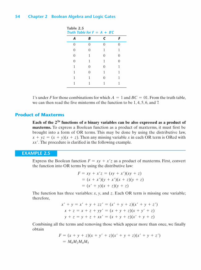
54 Chapter 2 Boolean Algebra and Logic Gates
1’s under F for those combinations for which A = 1 and BC = 01. From the truth table,
we can then read the five minterms of the function to be 1, 4, 5, 6, and 7.
Product of Maxterms
Each of the 22n functions of n binary variables can be also expressed as a product of maxterms. To express a Boolean function as a product of maxterms, it must first be
brought into a form of OR terms. This may be done by using the distributive law,
x + yz = (x + y)(x + z). Then any missing variable x in each OR term is ORed with
xx�. The procedure is clarified in the following example.
EXAMPLE 2.5
Express the Boolean function F = xy + x�z as a product of maxterms. First, convert
the function into OR terms by using the distributive law:
F = xy + x�z = (xy + x�)(xy + z)
= (x + x�)(y + x�)(x + z)(y + z)
= (x� + y)(x + z)(y + z)
The function has three variables: x, y, and z. Each OR term is missing one variable;
therefore,
x� + y = x� + y + zz� = (x� + y + z)(x� + y + z�)
x + z = x + z + yy� = (x + y + z)(x + y� + z)
y + z = y + z + xx� = (x + y + z)(x� + y + z)
Combining all the terms and removing those which appear more than once, we finally
obtain
F = (x + y + z)(x + y� + z)(x� + y + z)(x� + y + z�)
= M0M2M4M5
Table 2.5Truth Table for F � A � B�C
A B C F
0 0 0 0
0 0 1 1
0 1 0 0
0 1 1 0
1 0 0 1
1 0 1 1
1 1 0 1
1 1 1 1

Section 2.6 Canonical and Standard Forms 55
A convenient way to express this function is as follows:
F(x, y, z) = �(0, 2, 4, 5)
The product symbol, �, denotes the ANDing of maxterms; the numbers are the indices
of the maxterms of the function.
■
Conversion between Canonical Forms
The complement of a function expressed as the sum of minterms equals the sum of min-
terms missing from the original function. This is because the original function is expressed
by those minterms which make the function equal to 1, whereas its complement is a 1 for
those minterms for which the function is a 0. As an example, consider the function
F(A, B, C) = �(1, 4, 5, 6, 7)
This function has a complement that can be expressed as
F�(A, B, C) = �(0, 2, 3) = m0 + m2 + m3
Now, if we take the complement of F� by DeMorgan’s theorem, we obtain F in a differ-
ent form:
F = (m0 + m2 + m3)� = m=0# m=
2# m=
3 = M0M2M3 = �(0, 2, 3)
The last conversion follows from the definition of minterms and maxterms as shown in
Table 2.3 . From the table, it is clear that the following relation holds:
m=j = Mj
That is, the maxterm with subscript j is a complement of the minterm with the same subscript j and vice versa.
The last example demonstrates the conversion between a function expressed in sum‐
of‐minterms form and its equivalent in product‐of‐maxterms form. A similar argument
will show that the conversion between the product of maxterms and the sum of minterms
is similar. We now state a general conversion procedure: To convert from one canonical
form to another, interchange the symbols � and � and list those numbers missing from
the original form. In order to find the missing terms, one must realize that the total number
of minterms or maxterms is 2n, where n is the number of binary variables in the function.
A Boolean function can be converted from an algebraic expression to a product of
maxterms by means of a truth table and the canonical conversion procedure. Consider,
for example, the Boolean expression
F = xy + x�z
First, we derive the truth table of the function, as shown in Table 2.6 . The 1’s under F in
the table are determined from the combination of the variables for which xy = 11 or
xz = 01. The minterms of the function are read from the truth table to be 1, 3, 6, and 7.
The function expressed as a sum of minterms is
F(x, y, z) = �(1, 3, 6, 7)

56 Chapter 2 Boolean Algebra and Logic Gates
Since there is a total of eight minterms or maxterms in a function of three variables, we
determine the missing terms to be 0, 2, 4, and 5. The function expressed as a product of
maxterms is
F(x, y, z) = �(0, 2, 4, 5)
the same answer as obtained in Example 2.5.
Standard Forms
The two canonical forms of Boolean algebra are basic forms that one obtains from read-
ing a given function from the truth table. These forms are very seldom the ones with the
least number of literals, because each minterm or maxterm must contain, by definition,
all the variables, either complemented or uncomplemented.
Another way to express Boolean functions is in standard form. In this configuration,
the terms that form the function may contain one, two, or any number of literals. There
are two types of standard forms: the sum of products and products of sums.
The sum of products is a Boolean expression containing AND terms, called product terms, with one or more literals each. The sum denotes the ORing of these terms. An
example of a function expressed as a sum of products is
F1 = y� + xy + x�yz�
The expression has three product terms, with one, two, and three literals. Their sum is,
in effect, an OR operation.
The logic diagram of a sum‐of‐products expression consists of a group of AND gates
followed by a single OR gate. This configuration pattern is shown in Fig. 2.3 (a). Each
product term requires an AND gate, except for a term with a single literal. The logic sum
is formed with an OR gate whose inputs are the outputs of the AND gates and the
single literal. It is assumed that the input variables are directly available in their comple-
ments, so inverters are not included in the diagram. This circuit configuration is referred
to as a two‐level implementation.
Table 2.6Truth Table for F � xy � x�z
x y z F
0 0 0 0
0 0 1 1
0 1 0 0
0 1 1 1
1 0 0 0
1 0 1 0
1 1 0 1
1 1 1 1
Minterms
Maxterms

Section 2.6 Canonical and Standard Forms 57
A product of sums is a Boolean expression containing OR terms, called sum terms.
Each term may have any number of literals. The product denotes the ANDing of these
terms. An example of a function expressed as a product of sums is
F2 = x(y� + z)(x� + y + z�)
This expression has three sum terms, with one, two, and three literals. The product is an
AND operation. The use of the words product and sum stems from the similarity of the
AND operation to the arithmetic product (multiplication) and the similarity of the OR
operation to the arithmetic sum (addition). The gate structure of the product‐of‐sums
expression consists of a group of OR gates for the sum terms (except for a single literal),
followed by an AND gate, as shown in Fig. 2.3 (b). This standard type of expression results in a two‐level structure of gates.
A Boolean function may be expressed in a nonstandard form. For example, the function
F3 = AB + C(D + E)
is neither in sum‐of‐products nor in product‐of‐sums form. The implementation of this
expression is shown in Fig. 2.4 (a) and requires two AND gates and two OR gates. There
are three levels of gating in this circuit. It can be changed to a standard form by using
the distributive law to remove the parentheses:
F3 = AB + C(D + E) = AB + CD + CE
y�
F1
x�
z�y
xy
F2
x
y�
y
z
z
x�
(a) Sum of Products (b) Product of Sums
FIGURE 2.3Two‐level implementation
F3
A
B
CDE
(a) AB � C(D � E) (b) AB � CD � CE
A
F3
B
DC
CE
FIGURE 2.4Three‐ and two‐level implementation

58 Chapter 2 Boolean Algebra and Logic Gates
The sum‐of‐products expression is implemented in Fig. 2.4 (b). In general, a two‐level
implementation is preferred because it produces the least amount of delay through the
gates when the signal propagates from the inputs to the output. However, the number
of inputs to a given gate might not be practical.
2 . 7 O T H E R L O G I C O P E R AT I O N S
When the binary operators AND and OR are placed between two variables, x and y,
they form two Boolean functions, x # y and x + y, respectively. Previously we stated that
there are 22n functions for n binary variables. Thus, for two variables, n = 2, and the
number of possible Boolean functions is 16. Therefore, the AND and OR functions
are only 2 of a total of 16 possible functions formed with two binary variables. It would
be instructive to find the other 14 functions and investigate their properties.
The truth tables for the 16 functions formed with two binary variables are listed in
Table 2.7 . Each of the 16 columns, F0 to F15, represents a truth table of one possible func-
tion for the two variables, x and y. Note that the functions are determined from the
16 binary combinations that can be assigned to F. The 16 functions can be expressed
algebraically by means of Boolean functions, as is shown in the first column of Table 2.8 .
The Boolean expressions listed are simplified to their minimum number of literals.
Although each function can be expressed in terms of the Boolean operators AND,
OR, and NOT, there is no reason one cannot assign special operator symbols for express-
ing the other functions. Such operator symbols are listed in the second column of
Table 2.8 . However, of all the new symbols shown, only the exclusive‐OR symbol, �,
is in common use by digital designers.
Each of the functions in Table 2.8 is listed with an accompanying name and a com-
ment that explains the function in some way.1 The 16 functions listed can be subdivided
into three categories:
1. Two functions that produce a constant 0 or 1.
2. Four functions with unary operations: complement and transfer.
3. Ten functions with binary operators that define eight different operations: AND,
OR, NAND, NOR, exclusive‐OR, equivalence, inhibition, and implication.
Table 2.7Truth Tables for the 16 Functions of Two Binary Variables
x y F0 F1 F2 F3 F4 F5 F6 F7 F8 F9 F10 F11 F12 F13 F14 F15
0 0 0 0 0 0 0 0 0 0 1 1 1 1 1 1 1 1
0 1 0 0 0 0 1 1 1 1 0 0 0 0 1 1 1 1
1 0 0 0 1 1 0 0 1 1 0 0 1 1 0 0 1 1
1 1 0 1 0 1 0 1 0 1 0 1 0 1 0 1 0 1
1 The symbol ˆ is also used to indicate the exclusive or operator, e.g., xˆy. The symbol for the AND function is
sometimes omitted from the product of two variables, e.g., xy.

Section 2.7 Other Logic Operations 59
Constants for binary functions can be equal to only 1 or 0. The complement function
produces the complement of each of the binary variables. A function that is equal to an
input variable has been given the name transfer, because the variable x or y is transferred
through the gate that forms the function without changing its value. Of the eight binary
operators, two (inhibition and implication) are used by logicians, but are seldom used
in computer logic. The AND and OR operators have been mentioned in conjunction
with Boolean algebra. The other four functions are used extensively in the design of
digital systems.
The NOR function is the complement of the OR function, and its name is an
abbreviation of not‐OR. Similarly, NAND is the complement of AND and is an
abbreviation of not‐AND. The exclusive‐OR, abbreviated XOR, is similar to OR, but
excludes the combination of both x and y being equal to 1; it holds only when x and y differ in value. (It is sometimes referred to as the binary difference operator.) Equiv-
alence is a function that is 1 when the two binary variables are equal (i.e., when both
are 0 or both are 1). The exclusive‐OR and equivalence functions are the comple-
ments of each other. This can be easily verified by inspecting Table 2.7 : The truth
table for exclusive‐OR is F6 and for equivalence is F9, and these two functions are
the complements of each other. For this reason, the equivalence function is called
exclusive‐NOR, abbreviated XNOR.
Table 2.8Boolean Expressions for the 16 Functions of Two Variables
Boolean FunctionsOperator Symbol Name Comments
F0 = 0 Null Binary constant 0
F1 = xy x # y AND x and y
F2 = xy� x/y Inhibition x, but not y
F3 = x Transfer x
F4 = x�y y/x Inhibition y, but not x
F5 = y Transfer y
F6 = xy� + x�y x � y Exclusive‐OR x or y, but not both
F7 = x + y x + y OR x or y
F8 = (x + y)� x T y NOR Not‐OR
F9 = xy + x�y� (x � y)� Equivalence x equals y
F10 = y� y� Complement Not y
F11 = x + y� x � y Implication If y, then x
F12 = x� x� Complement Not x
F13 = x� + y x � y Implication If x, then y
F14 = (xy)� x c y NAND Not‐AND
F15 = 1 Identity Binary constant 1

60 Chapter 2 Boolean Algebra and Logic Gates
Boolean algebra, as defined in Section 2.2, has two binary operators, which we have
called AND and OR, and a unary operator, NOT (complement). From the definitions,
we have deduced a number of properties of these operators and now have defined other
binary operators in terms of them. There is nothing unique about this procedure. We
could have just as well started with the operator NOR (T), for example, and later
defined AND, OR, and NOT in terms of it. There are, nevertheless, good reasons for
introducing Boolean algebra in the way it has been introduced. The concepts of “and,”
“or,” and “not” are familiar and are used by people to express everyday logical ideas.
Moreover, the Huntington postulates reflect the dual nature of the algebra, emphasizing
the symmetry of + and # with respect to each other.
2 . 8 D I G I TA L L O G I C G AT E S
Since Boolean functions are expressed in terms of AND, OR, and NOT operations, it is
easier to implement a Boolean function with these type of gates. Still, the possibility of
constructing gates for the other logic operations is of practical interest. Factors to be
weighed in considering the construction of other types of logic gates are (1) the feasibil-
ity and economy of producing the gate with physical components, (2) the possibility of
extending the gate to more than two inputs, (3) the basic properties of the binary oper-
ator, such as commutativity and associativity, and (4) the ability of the gate to implement
Boolean functions alone or in conjunction with other gates.
Of the 16 functions defined in Table 2.8 , two are equal to a constant and four are
repeated. There are only 10 functions left to be considered as candidates for logic gates.
Two—inhibition and implication—are not commutative or associative and thus are
impractical to use as standard logic gates. The other eight—complement, transfer, AND,
OR, NAND, NOR, exclusive‐OR, and equivalence—are used as standard gates in
digital design.
The graphic symbols and truth tables of the eight gates are shown in Fig. 2.5 . Each
gate has one or two binary input variables, designated by x and y, and one binary output
variable, designated by F. The AND, OR, and inverter circuits were defined in Fig. 1.6.
The inverter circuit inverts the logic sense of a binary variable, producing the NOT, or
complement, function. The small circle in the output of the graphic symbol of an inverter
(referred to as a bubble) designates the logic complement. The triangle symbol by itself
designates a buffer circuit. A buffer produces the transfer function, but does not produce
a logic operation, since the binary value of the output is equal to the binary value of the
input. This circuit is used for power amplification of the signal and is equivalent to two
inverters connected in cascade.
The NAND function is the complement of the AND function, as indicated by a
graphic symbol that consists of an AND graphic symbol followed by a small circle. The
NOR function is the complement of the OR function and uses an OR graphic symbol
followed by a small circle. NAND and NOR gates are used extensively as standard logic
gates and are in fact far more popular than the AND and OR gates. This is because
NAND and NOR gates are easily constructed with transistor circuits and because digital
circuits can be easily implemented with them.

Section 2.8 Digital Logic Gates 61
NameGraphicsymbol
Algebraicfunction
Truthtable
AND
OR
Inverter
Buffer
NAND
NOR
Exclusive-OR(XOR)
Exclusive-NORor
equivalence
F � x · y
F � x � y
F � (xy)�
F � x�
F � x
x y F
x y F
x y F
x y F
x y F
x y F
x F
x F
F � (x � y)�
F � xy� � x�y
F � xy � x�y�
F
F
Fx
Fx
F
F
F
Fx
y
xy
xy � x � y
� (x � y)�
0011
0101
0011
0101
0111
01
10
01
01
0011
0101
1110
0011
0101
1000
0011
0101
0110
0011
0101
1001
0001
xy
xy
xy
FIGURE 2.5Digital logic gates

62 Chapter 2 Boolean Algebra and Logic Gates
The exclusive‐OR gate has a graphic symbol similar to that of the OR gate, except
for the additional curved line on the input side. The equivalence, or exclusive‐NOR, gate
is the complement of the exclusive‐OR, as indicated by the small circle on the output
side of the graphic symbol.
Extension to Multiple Inputs
The gates shown in Fig. 2.5 —except for the inverter and buffer—can be extended to
have more than two inputs. A gate can be extended to have multiple inputs if the binary
operation it represents is commutative and associative. The AND and OR operations,
defined in Boolean algebra, possess these two properties. For the OR function, we have
x + y = y + x (commutative)
and
(x + y) + z = x + (y + z) = x + y + z (associative)
which indicates that the gate inputs can be interchanged and that the OR function can
be extended to three or more variables.
The NAND and NOR functions are commutative, and their gates can be extended
to have more than two inputs, provided that the definition of the operation is modified
slightly. The difficulty is that the NAND and NOR operators are not associative
(i.e., (x T y) T z � x T (y T z) ), as shown in Fig. 2.6 and the following equations:
(x T y) T z = [(x + y)� + z]� = (x + y)z� = xz� + yz�
x T (y T z) = [x + (y + z)�]� = x�(y + z) = x�y + x�z
To overcome this difficulty, we define the multiple NOR (or NAND) gate as a
complemented OR (or AND) gate. Thus, by definition, we have
x T y T z = (x + y + z)�
x c y c z = (xyz)�
The graphic symbols for the three‐input gates are shown in Fig. 2.7 . In writing cascaded
NOR and NAND operations, one must use the correct parentheses to signify the proper
sequence of the gates. To demonstrate this principle, consider the circuit of Fig. 2.7 (c).
The Boolean function for the circuit must be written as
F = [(ABC)�(DE)�]� = ABC + DE
The second expression is obtained from one of DeMorgan’s theorems. It also shows that
an expression in sum‐of‐products form can be implemented with NAND gates. (NAND
and NOR gates are discussed further in Section 3.7.)
The exclusive‐OR and equivalence gates are both commutative and associative and
can be extended to more than two inputs. However, multiple‐input exclusive‐OR gates
are uncommon from the hardware standpoint. In fact, even a two‐input function is usu-
ally constructed with other types of gates. Moreover, the definition of the function must
be modified when extended to more than two variables. Exclusive‐OR is an odd function
(i.e., it is equal to 1 if the input variables have an odd number of 1’s). The construction

Section 2.8 Digital Logic Gates 63
of a three‐input exclusive‐OR function is shown in Fig. 2.8 . This function is normally
implemented by cascading two‐input gates, as shown in (a). Graphically, it can be
represented with a single three‐input gate, as shown in (b). The truth table in (c) clearly
indicates that the output F is equal to 1 if only one input is equal to 1 or if all three inputs
are equal to 1 (i.e., when the total number of 1’s in the input variables is odd). (Exclusive‐
OR gates are discussed further in Section 3.9.)
Positive and Negative Logic
The binary signal at the inputs and outputs of any gate has one of two values, except
during transition. One signal value represents logic 1 and the other logic 0. Since two
signal values are assigned to two logic values, there exist two different assignments of
(x y) z � (x � y)z�
x
y
y
x (y z) � x� (y � z)x
y
z
FIGURE 2.6Demonstrating the nonassociativity of the NOR operator: (x T y) T z � x T (y T z)
(a) 3-input NOR gate
y (x � y � z)�x
z
(b) 3-input NAND gate
(xyz)�yx
z
(c) Cascaded NAND gates
D
B
F � [(ABC)� � (DE)�]� � ABC � DE
A
C
E
FIGURE 2.7Multiple‐input and cascaded NOR and NAND gates

64 Chapter 2 Boolean Algebra and Logic Gates
signal level to logic value, as shown in Fig. 2.9 . The higher signal level is designated by
H and the lower signal level by L. Choosing the high‐level H to represent logic 1 defines a positive logic system. Choosing the low‐level L to represent logic 1 defines a negative logic system. The terms positive and negative are somewhat misleading, since both sig-
nals may be positive or both may be negative. It is not the actual values of the signals
that determine the type of logic, but rather the assignment of logic values to the relative
amplitudes of the two signal levels.
Hardware digital gates are defined in terms of signal values such as H and L. It is up
to the user to decide on a positive or negative logic polarity. Consider, for example, the
electronic gate shown in Fig. 2.10 (b). The truth table for this gate is listed in Fig. 2.10 (a).
It specifies the physical behavior of the gate when H is 3 V and L is 0 V. The truth table
of Fig. 2.10 (c) assumes a positive logic assignment, with H = 1 and L = 0. This truth
table is the same as the one for the AND operation. The graphic symbol for a positive
logic AND gate is shown in Fig. 2.10 (d).
Now consider the negative logic assignment for the same physical gate with L = 1
and H = 0. The result is the truth table of Fig. 2.10 (e). This table represents the OR
operation, even though the entries are reversed. The graphic symbol for the negative‐
logic OR gate is shown in Fig. 2.10 (f). The small triangles in the inputs and output
(a) Using 2-input gates
(b) 3-input gate(c) Truth table
xF � x � y � zy
z
y
zF � x � y � z
xx y z F
0
0
00
11
1
1
0
1
10
10
0
1
0
1
01
01
0
1
011
0
0
1
0
1
FIGURE 2.8Three‐input exclusive‐OR gate
(a) Positive logic
Logicvalue
1
0
Signalvalue
H
L(b) Negative logic
Logicvalue
0
1
Signalvalue
H
L
FIGURE 2.9Signal assignment and logic polarity

Section 2.8 Digital Logic Gates 65
designate a polarity indicator, the presence of which along a terminal signifies that
negative logic is assumed for the signal. Thus, the same physical gate can operate either
as a positive‐logic AND gate or as a negative‐logic OR gate.
The conversion from positive logic to negative logic and vice versa is essentially
an operation that changes 1’s to 0’s and 0’s to 1’s in both the inputs and the output
of a gate. Since this operation produces the dual of a function, the change of all ter-
minals from one polarity to the other results in taking the dual of the function. The
upshot is that all AND operations are converted to OR operations (or graphic sym-
bols) and vice versa. In addition, one must not forget to include the polarity‐indicator
triangle in the graphic symbols when negative logic is assumed. In this book, we will
not use negative logic gates and will assume that all gates operate with a positive logic
assignment.
(c) Truth table for positive logic
(e) Truth table for negative logic
(d) Positive logic AND gate
(f) Negative logic OR gate
(b) Gate block diagram
xzDigital
gatey
zx
y
zx
y
(a) Truth table with H and L
x y z
LLLL L
LLHH
H
HH
x y z
000
0 0
0011
1
11
x y z
111
1 1
1100
0
00
FIGURE 2.10Demonstration of positive and negative logic

66 Chapter 2 Boolean Algebra and Logic Gates
2 . 9 I N T E G R AT E D C I R C U I T S
An integrated circuit (IC) is fabricated on a die of a silicon semiconductor crystal, called
a chip, containing the electronic components for constructing digital gates. The complex
chemical and physical processes used to form a semiconductor circuit are not a subject
of this book. The various gates are interconnected inside the chip to form the required
circuit. The chip is mounted in a ceramic or plastic container, and connections are welded
to external pins to form the integrated circuit. The number of pins may range from 14
on a small IC package to several thousand on a larger package. Each IC has a numeric
designation printed on the surface of the package for identification. Vendors provide
data books, catalogs, and Internet websites that contain descriptions and information
about the ICs that they manufacture.
Levels of Integration
Digital ICs are often categorized according to the complexity of their circuits, as mea-
sured by the number of logic gates in a single package. The differentiation between those
chips which have a few internal gates and those having hundreds of thousands of gates
is made by customary reference to a package as being either a small‐, medium‐, large‐,
or very large‐scale integration device.
Small‐scale integration (SSI) devices contain several independent gates in a single
package. The inputs and outputs of the gates are connected directly to the pins in the
package. The number of gates is usually fewer than 10 and is limited by the number of
pins available in the IC.
Medium‐scale integration (MSI) devices have a complexity of approximately 10 to
1,000 gates in a single package. They usually perform specific elementary digital opera-
tions. MSI digital functions are introduced in Chapter 4 as decoders, adders, and multi-
plexers and in Chapter 6 as registers and counters.
Large‐scale integration (LSI) devices contain thousands of gates in a single package.
They include digital systems such as processors, memory chips, and programmable logic
devices. Some LSI components are presented in Chapter 7 .
Very large‐scale integration (VLSI) devices now contain millions of gates within a
single package. Examples are large memory arrays and complex microcomputer chips.
Because of their small size and low cost, VLSI devices have revolutionized the computer
system design technology, giving the designer the capability to create structures that
were previously uneconomical to build.
Digital Logic Families
Digital integrated circuits are classified not only by their complexity or logical operation,
but also by the specific circuit technology to which they belong. The circuit technology
is referred to as a digital logic family. Each logic family has its own basic electronic
circuit upon which more complex digital circuits and components are developed. The
basic circuit in each technology is a NAND, NOR, or inverter gate. The electronic

Section 2.9 Integrated Circuits 67
components employed in the construction of the basic circuit are usually used to name
the technology. Many different logic families of digital integrated circuits have been
introduced commercially. The following are the most popular:
TTL transistor–transistor logic;
ECL emitter‐coupled logic;
MOS metal‐oxide semiconductor;
CMOS complementary metal‐oxide semiconductor.
TTL is a logic family that has been in use for 50 years and is considered to be stan-
dard. ECL has an advantage in systems requiring high‐speed operation. MOS is suitable
for circuits that need high component density, and CMOS is preferable in systems
requiring low power consumption, such as digital cameras, personal media players, and
other handheld portable devices. Low power consumption is essential for VLSI design;
therefore, CMOS has become the dominant logic family, while TTL and ECL continue
to decline in use. The most important parameters distinguishing logic families are listed
below; CMOS integrated circuits are discussed briefly in the appendix.
Fan‐out specifies the number of standard loads that the output of a typical gate can
drive without impairing its normal operation. A standard load is usually defined as the
amount of current needed by an input of another similar gate in the same family.
Fan‐in is the number of inputs available in a gate.
Power dissipation is the power consumed by the gate that must be available from the
power supply.
Propagation delay is the average transition delay time for a signal to propagate from
input to output. For example, if the input of an inverter switches from 0 to 1, the output
will switch from 1 to 0, but after a time determined by the propagation delay of the
device. The operating speed is inversely proportional to the propagation delay.
Noise margin is the maximum external noise voltage added to an input signal that
does not cause an undesirable change in the circuit output.
Computer‐Aided Design of VLSI Circuits
Integrated circuits having submicron geometric features are manufactured by optically
projecting patterns of light onto silicon wafers. Prior to exposure, the wafers are coated
with a photoresistive material that either hardens or softens when exposed to light.
Removing extraneous photoresist leaves patterns of exposed silicon. The exposed
regions are then implanted with dopant atoms to create a semiconductor material hav-
ing the electrical properties of transistors and the logical properties of gates. The design
process translates a functional specification or description of the circuit (i.e., what it must
do) into a physical specification or description (how it must be implemented in silicon).
The design of digital systems with VLSI circuits containing millions of transistors and
gates is an enormous and formidable task. Systems of this complexity are usually impos-
sible to develop and verify without the assistance of computer‐aided design (CAD)

68 Chapter 2 Boolean Algebra and Logic Gates
tools, which consist of software programs that support computer‐based representations
of circuits and aid in the development of digital hardware by automating the design
process. Electronic design automation (EDA) covers all phases of the design of inte-
grated circuits. A typical design flow for creating VLSI circuits consists of a sequence of
steps beginning with design entry (e.g., entering a schematic) and culminating with the
generation of the database that contains the photomask used to fabricate the IC. There
are a variety of options available for creating the physical realization of a digital circuit
in silicon. The designer can choose between an application‐specific integrated circuit
(ASIC), a field‐programmable gate array (FPGA), a programmable logic device (PLD),
and a full‐custom IC. With each of these devices comes a set of CAD tools that provide
the necessary software to facilitate the hardware fabrication of the unit. Each of these
technologies has a market niche determined by the size of the market and the unit cost
of the devices that are required to implement a design.
Some CAD systems include an editing program for creating and modifying schematic
diagrams on a computer screen. This process is called schematic capture or schematic
entry. With the aid of menus, keyboard commands, and a mouse, a schematic editor can
draw circuit diagrams of digital circuits on the computer screen. Components can be
placed on the screen from a list in an internal library and can then be connected with
lines that represent wires. The schematic entry software creates and manages a database
containing the information produced with the schematic. Primitive gates and functional
blocks have associated models that allow the functionality (i.e., logical behavior) and
timing of the circuit to be verified. Verification is performed by applying inputs to the
circuit and using a logic simulator to determine and display the outputs in text or wave-
form format.
An important development in the design of digital systems is the use of a hardware
description language (HDL). Such a language resembles a computer programming
language, but is specifically oriented to describing digital hardware. It represents logic
diagrams and other digital information in textual form to describe the functionality
and structure of a circuit. Moreover, the HDL description of a circuit’s functionality
can be abstract, without reference to specific hardware, thereby freeing a designer to
devote attention to higher level functional detail (e.g., under certain conditions the
circuit must detect a particular pattern of 1’s and 0’s in a serial bit stream of data) rather
than transistor‐level detail. HDL‐based models of a circuit or system are simulated to
check and verify its functionality before it is submitted to fabrication, thereby reducing
the risk and waste of manufacturing a circuit that fails to operate correctly. In tandem
with the emergence of HDL‐based design languages, tools have been developed to
automatically and optimally synthesize the logic described by an HDL model of a
circuit. These two advances in technology have led to an almost total reliance by indus-try on HDL‐based synthesis tools and methodologies for the design of the circuits of complex digital systems. Two HDLs—Verilog and VHDL—have been approved as
standards by the Institute of Electronics and Electrical Engineers (IEEE) and are in
use by design teams worldwide. The Verilog HDL is introduced in Section 3.10, and
because of its importance, we include several exercises and design problems based on
Verilog throughout the book.

Problems 69
P R O B L E M S
(Answers to problems marked with * appear at the end of the text.)
2.1 Demonstrate the validity of the following identities by means of truth tables:
(a) DeMorgan’s theorem for three variables: (x + y + z)� = x�y�z� and (xyz)� =x� + y� + z�
(b) The distributive law: x + yz = ( x + y )( x + z )
(c) The distributive law: x(y + z) = xy + xz
(d) The associative law: x + (y + z) = (x + y) + z
(e) The associative law and x(yz) = (xy)z
2.2 Simplify the following Boolean expressions to a minimum number of literals:
(a) * xy + xy � (b) * (x + y) (x + y�)
(c) * xyz + x � y + xyz � (d) * (A + B)� (A� + B�)� (e) (a + b + c�)(a� b� + c) (f) a�bc + abc� + abc + a�bc�
2.3 Simplify the following Boolean expressions to a minimum number of literals:
(a) * ABC + A�B + ABC� (b)* x � yz + xz
(c) * (x + y)� (x� + y�) (d) * xy + x(wz + wz�)
(e) * (BC� + A�D) (AB� + CD�) (f) (a� + c�) (a + b� + c�)
2.4 Reduce the following Boolean expressions to the indicated number of literals:
(a) * A�C� + ABC + AC� to three literals
(b) * (x�y� + z)� + z + xy + wz to three literals
(c) * A�B(D� + C�D) + B(A + A�CD) to one literal
(d) * (A� + C) (A� + C�) (A + B + C�D) to four literals
(e) ABC'D + A'BD + ABCD to two literals
2.5 Draw logic diagrams of the circuits that implement the original and simplified expressions
in Problem 2.2.
2.6 Draw logic diagrams of the circuits that implement the original and simplified expressions
in Problem 2.3.
2.7 Draw logic diagrams of the circuits that implement the original and simplified expressions
in Problem 2.4.
2.8 Find the complement of F = wx + yz; then show that FF� = 0 and F + F� = 1.
2.9 Find the complement of the following expressions:
(a) * xy� + x�y (b) (a + c) (a + b�) (a� + b + c�)
(c) z + z�(v�w + xy)
2.10 Given the Boolean functions F1 and F 2 , show that
(a) The Boolean function E = F1 + F2 contains the sum of the minterms of F1 and F2.
(b) The Boolean function G = F1F2 contains only the minterms that are common to F1
and F2.
2.11 List the truth table of the function:
(a) * F = xy + xy� + y�z (b) F = bc + a�c�
2.12 We can perform logical operations on strings of bits by considering each pair of correspond-
ing bits separately (called bitwise operation). Given two eight‐bit strings A = 10110001
and B = 10101100, evaluate the eight‐bit result after the following logical operations:
(a)* AND (b) OR (c)* XOR (d)* NOT A (e) NOT B

70 Chapter 2 Boolean Algebra and Logic Gates
2.13 Draw logic diagrams to implement the following Boolean expressions:
(a) y = [(u + x�) (y� + z)]
(b) y = (u � y)� + x
(c) y = (u� + x�) (y + z�)
(d) y = u(x � z) + y� (e) y = u + yz + uxy
(f) y = u + x + x�(u + y�)
2.14 Implement the Boolean function
F = xy + x�y� + y�z
(a) With AND, OR, and inverter gates
(b) * With OR and inverter gates
(c) With AND and inverter gates
(d) With NAND and inverter gates
(e) With NOR and inverter gates
2.15* Simplify the following Boolean functions T1 and T2 to a minimum number of literals:
A B C T 1 T 2
0 0 0 1 0 0 0 1 1 0
0 1 0 1 0
0 1 1 0 1
1 0 0 0 1
1 0 1 0 1
1 1 0 0 1
1 1 1 0 1
2.16 The logical sum of all minterms of a Boolean function of n variables is 1.
(a) Prove the previous statement for n = 3.
(b) Suggest a procedure for a general proof.
2.17 Obtain the truth table of the following functions, and express each function in sum‐of‐min-
terms and product‐of‐maxterms form:
(a) * (b + cd)(c + bd) (b) (cd + b�c + bd�)(b + d)
(c) (c� + d)(b + c�) (d) bd� + acd� + ab�c + a�c�
2.18 For the Boolean function
F = xy�z + x�y�z + w�xy + wx�y + wxy
(a) Obtain the truth table of F. (b) Draw the logic diagram, using the original Boolean expression.
(c) * Use Boolean algebra to simplify the function to a minimum number of literals.
(d) Obtain the truth table of the function from the simplified expression and show that
it is the same as the one in part (a).
(e) Draw the logic diagram from the simplified expression, and compare the total number
of gates with the diagram of part (b).

Problems 71
2.19* Express the following function as a sum of minterms and as a product of maxterms:
F(A, B, C, D) = B�D + A�D + BD
2.20 Express the complement of the following functions in sum‐of‐minterms form:
(a) F(A,B ,C, D) = g(2, 4, 7, 10, 12, 14)
(b) F ( x, y, z ) = w (3, 5, 7)
2.21 Convert each of the following to the other canonical form:
(a) F(x, y, z) = g(1, 3, 5)
(b) F(A, B, C, D) = w (3, 5, 8, 11)
2.22* Convert each of the following expressions into sum of products and product of sums:
(a) ( u + xw )( x + u�v )
(b) x� + x(x + y�)(y + z�)
2.23 Draw the logic diagram corresponding to the following Boolean expressions without sim-
plifying them:
(a) BC� + AB + ACD
(b) (A + B)(C + D)(A� + B + D)
(c) (AB + A�B�)(CD� + C�D)
(d) A + CD + (A + D')(C' + D)
2.24 Show that the dual of the exclusive‐OR is equal to its complement.
2.25 By substituting the Boolean expression equivalent of the binary operations as defined in
Table 2.8 , show the following:
(a) The inhibition operation is neither commutative nor associative.
(b) The exclusive‐OR operation is commutative and associative.
2.26 Show that a positive logic NAND gate is a negative logic NOR gate and vice versa.
2.27 Write the Boolean equations and draw the logic diagram of the circuit whose outputs are
defined by the following truth table:
Table P2.27
f 1 f 2 a b c
1 1 0 0 0
0 1 0 0 1
1 0 0 1 0
1 1 0 1 1
1 0 1 0 0
0 1 1 0 1
1 0 1 1 1
2.28 Write Boolean expressions and construct the truth tables describing the outputs of the
circuits described by the logic diagrams in Fig. P2.28.
2.29 Determine whether the following Boolean equation is true or false.
x�y� + x�z + x�z� = x�z� + y�z� + x�z

72 Chapter 2 Boolean Algebra and Logic Gates
2.30 Write the following Boolean expressions in sum of products form:
(b + d)(a� + b� + c)
2.31 Write the following Boolean expression in product of sums form:
a�b + a�c� + abc
R E F E R E N C E S
1. B oole, G. 1854. An Investigation of the Laws of Thought. New York: Dover.
2. D ietmeyer, D. L. 1988. Logic Design of Digital Systems, 3rd ed. Boston: Allyn and Bacon.
3. H untington, E. V. Sets of independent postulates for the algebra of logic. Trans. Am. Math. Soc., 5 (1904): 288–309.
4. IEEE Standard Hardware Description Language Based on the Verilog Hardware Descrip-tion Language, Language Reference Manual (LRM), IEEE Std.1364‐1995, 1996, 2001,
2005, The Institute of Electrical and Electronics Engineers, Piscataway, NJ.
5. IEEE Standard VHDL Language Reference Manual (LRM), IEEE Std. 1076‐1987, 1988,
The Institute of Electrical and Electronics Engineers, Piscataway, NJ.
6. M ano, M. M. and C. R. K ime . 2000. Logic and Computer Design Fundamentals, 2nd ed.
Upper Saddle River, NJ: Prentice Hall.
7. S hannon, C. E. A symbolic analysis of relay and switching circuits. Trans. AIEE, 57 (1938):
713–723.
WEB SEARCH TOP ICS
Algebraic field
Boolean logic
Boolean gates
Bipolar transistor
Field-effect transistor
Emitter-coupled logic
TTL logic
CMOS logic
CMOS process
a
b
c
d
e
y
a
b
c
d
e
f
y2
y1
(b)(a)
FIGURE P2.28