Exploiting dynamic reconfiguration of platform FPGAs: implementation issues
8
Exploiting dynamic reconfiguration of platform FPGAs: Implementation issues Miguel L. Silva 1 and Jo˜ ao Canas Ferreira 1,2 1 FEUP/DEEC 2 INESC Porto Rua Dr. Roberto Frias, s/n Rua Dr. Roberto Frias, s/n 4200-465 PORTO, Portugal 4200-465 PORTO, Portugal [email protected] [email protected] Abstract The effective use of dynamic reconfiguration re- quires the designer to address many implementation issues. The market introduction of feature-full plat- form FPGAs equipped with embedded CPU blocks ex- pands the number of situations where dynamic reconfig- uration may be applied to improve overall performance and logic utilization. The paper compares the design of two similar systems supporting dynamic reconfigu- ration and the issues that were addressed in their im- plementation. The first system supports 32-bit data transfers between CPU and the dynamically reconfig- urable circuits. The other implementation supports 64- bit transfers, but its effective use is more complicated and several restrictions must be taken into account. The work includes a performance comparison of the two designs on several simple tasks, including pattern matching, image processing and hashing. 1 Introduction The present work is concerned with the implemen- tation issues that arise for designs that try to ex- ploit some platform FPGA’s capability for configura- tion changes at run-time. The intent is typically to time-share the available hardware to support multiple (and mutually exclusive) tasks; alternatively, the de- signer may be seeking better performance by adapting the hardware implementation to the actual data being processed at a given instant. Work partially funded by the Department of Electrical and Com- puter Engineering of the Faculty of Engineering of the University of Porto, under contract DEEC-ID/05/2003, and by FCT schol- arship SFRH/BD/17029/2004. In the context of the present work, we are interested in designs that contain a closely-coupled CPU, typi- cally as a dedicated block or as a core implemented on part of the reconfigurable fabric. There are many hardware and software issues that must be considered in this context. The present work deals mainly with the need to establish an appropriate hardware environ- ment in order to be able to carry out dynamic reconfig- urations in an orderly fashion, and how the associated design choices affect the global performance. Since the actual details of the underlying reconfigurable platform may be important for the concrete analysis of the is- sues, the paper presents its discussion in the context of systems based on Virtex-II Pro devices, an advanced FPGA family from Xilinx. The paper is organized around two actual system designs with similar overall organization. The first one is implemented on a XC2VP7-FG456-6 device and fea- tures a 32-bit data bus; the second one is implemented on a XC2VP30-FF896-7 and uses a 64-bit bus. The second system design was intended to implement the same basic approach as the first one, but to achieve better performance for tasks that depend on run-time reconfiguration. Other systems based on dynamically reconfigurable platform FPGAs have been described in the literature (see, for instance, [13, 2, 1, 11]). Aspects of the 32-bit design used for this work have been presented in [5]. The 64-bit system is described here for the first time. The rest of the paper is organized as follows. Sec- tion 2 describes the overall context of the work and presents the global design choices. The 32-bit system is summarized in section 3, which also characterizes the system’s performance and presents experimental results for some simple application fragments. Section 4 then describes the 64-bit system, with emphasis on 1-4244-0054-6/06/$20.00 ©2006 IEEE
-
Upload
independent -
Category
Documents
-
view
5 -
download
0
Transcript of Exploiting dynamic reconfiguration of platform FPGAs: implementation issues
Exploiting dynamic reconfiguration of platform FPGAs:
Implementation issues
Miguel L. Silva1 and Joao Canas Ferreira1,2
1FEUP/DEEC 2INESC PortoRua Dr. Roberto Frias, s/n Rua Dr. Roberto Frias, s/n4200-465 PORTO, Portugal 4200-465 PORTO, Portugal
[email protected] [email protected]
Abstract
The effective use of dynamic reconfiguration re-
quires the designer to address many implementation
issues. The market introduction of feature-full plat-
form FPGAs equipped with embedded CPU blocks ex-
pands the number of situations where dynamic reconfig-
uration may be applied to improve overall performance
and logic utilization. The paper compares the design
of two similar systems supporting dynamic reconfigu-
ration and the issues that were addressed in their im-
plementation. The first system supports 32-bit data
transfers between CPU and the dynamically reconfig-
urable circuits. The other implementation supports 64-
bit transfers, but its effective use is more complicated
and several restrictions must be taken into account.
The work includes a performance comparison of the
two designs on several simple tasks, including pattern
matching, image processing and hashing.
1 Introduction
The present work is concerned with the implemen-tation issues that arise for designs that try to ex-ploit some platform FPGA’s capability for configura-tion changes at run-time. The intent is typically totime-share the available hardware to support multiple(and mutually exclusive) tasks; alternatively, the de-signer may be seeking better performance by adaptingthe hardware implementation to the actual data beingprocessed at a given instant.
Work partially funded by the Department of Electrical and Com-puter Engineering of the Faculty of Engineering of the Universityof Porto, under contract DEEC-ID/05/2003, and by FCT schol-arship SFRH/BD/17029/2004.
In the context of the present work, we are interestedin designs that contain a closely-coupled CPU, typi-cally as a dedicated block or as a core implementedon part of the reconfigurable fabric. There are manyhardware and software issues that must be consideredin this context. The present work deals mainly withthe need to establish an appropriate hardware environ-ment in order to be able to carry out dynamic reconfig-urations in an orderly fashion, and how the associateddesign choices affect the global performance. Since theactual details of the underlying reconfigurable platformmay be important for the concrete analysis of the is-sues, the paper presents its discussion in the context ofsystems based on Virtex-II Pro devices, an advancedFPGA family from Xilinx.
The paper is organized around two actual systemdesigns with similar overall organization. The first oneis implemented on a XC2VP7-FG456-6 device and fea-tures a 32-bit data bus; the second one is implementedon a XC2VP30-FF896-7 and uses a 64-bit bus. Thesecond system design was intended to implement thesame basic approach as the first one, but to achievebetter performance for tasks that depend on run-timereconfiguration.
Other systems based on dynamically reconfigurableplatform FPGAs have been described in the literature(see, for instance, [13, 2, 1, 11]). Aspects of the 32-bitdesign used for this work have been presented in [5].The 64-bit system is described here for the first time.
The rest of the paper is organized as follows. Sec-tion 2 describes the overall context of the work andpresents the global design choices. The 32-bit systemis summarized in section 3, which also characterizesthe system’s performance and presents experimentalresults for some simple application fragments. Section4 then describes the 64-bit system, with emphasis on
1-4244-0054-6/06/$20.00 ©2006 IEEE

Figure 1. General system architecture
the different design choices and how they impacted thesystem’s performance. The section also presents exper-imental results, including results for the same applica-tion fragments used with the 32-bit version. Finally,section 5 presents some final remarks and concludesthe paper.
2 Dynamic reconfiguration of platform
FPGAs
2.1 Generic system organization
A generic overview of a system organization used forthis work is shown in figure 1. In addition to the CPUand the area for run-time reconfiguration (the dynamicarea), the following modules are included:
• Memory interface unit. Depending on theneeds, it may interface to internal and/or exter-nal memory. Both types of memory may store re-configuration data (for the dynamic modules) andapplication-specific data.
• Configuration control unit. This module per-forms the actual reconfiguration of the dynamicarea. It can be seen as an interface unit to theFPGA’s configuration memory.
• External communication unit. This module,if available, is responsible for communications withan external system (e.g., a standalone computer)for data transfer, system control and debuggingoperations.
• Dynamic area communication unit. This unitis responsible for communications with the mod-ules in the dynamic area. It includes the circuitryto use one of the data busses and, possibly, a DMAcontroller.
2.2 Partial configurations
The process of reconfiguring the dynamic area musthandle the constraints imposed by the FPGA’s archi-tecture. Virtex-II Pro devices (like other Xilinx de-vices) are reconfigured by frames. A frame is a set ofconfiguration bits that control a column of configurableresources. Each such column covers the entire heightof the device. However, in practice, it is difficult tohave a dynamic area that covers the entire height ofthe device, because that would isolate one side of thedevice from the other, i.e., circuits on the left of thedynamic area would not be able to connect to circuitson the left, and vice-versa. This may not be acceptablein practice. For instance, the layout of the board mayconstrain the layout of the resources inside the FPGAin such a way as to make a full-height dynamic regionunavailable (typically because some external compo-nents are connected to pins on the upper or lower sidesof the reconfigurable fabric).
Due to the need to take such layout constraints inconsideration, a dynamic area will typically not occupythe full height of the device. Therefore, the partial con-figurations used to reconfigure the dynamic area mustbe produced in such a way as to not disturb the circuitsbelow or above.
Another issue with the reconfiguration process arisesbecause partial configurations are “differential” config-urations, that is, they assume an initial state of theconfiguration resources, and only specify reconfigura-tion data for those resources whose state is to be dif-ferent from the initial one. Since the dynamic areais used for multiple configurations in an order that isunknown at the time the partial configurations are pro-duced, the problem of ensuring the correct state priorto reconfiguration arises.
Several ways to address the problem have been re-ported [11, 6, 10, 12]. One way is to have a tool likeBitLinker [12], that is capable of ensuring that theconfiguration bitstream is complete (i.e., not “differ-ential”). This has the side effect of increasing the con-figuration time.
The use of a configuration assembly tool may helpsolve other problems. For instance, BitLinker ensuresthat partial configurations do not disturb the circuitsresiding below or above the dynamic area.
It is possible to go further and provide means for as-sembling the correct partial configuration from the con-figurations of individual components [12, 6, 10]. In thisway, components can be reused without going throughthe complete high-level design flow. This is particu-larly helpful when multiple similar configurations mustbe produced. All the configurations used in the experi-

Figure 2. LUT-based bus macros
ments reported in the next sections have been producedwith the help of BitLinker.
The assembly of component configurations rises theproblem of establishing communications between them.This requires a means of ensuring that the compo-nent’s input and output ports are at fixed locations,so that the assembled configuration can be producedby appropriate concatenation of the individual com-ponents. To ensure that a component has input andoutput ports compatible with the assembly procedure,a so-called “bus macro” is used in the component’s de-sign. Figure 2 illustrates the situation. In this particu-lar case, the communication is guaranteed by ensuringthat the output signals of component A (called In(0)
and In(1)) flow out of the component through spe-cific LUTs and that the input signals of component B(called Out(0) and Out(1)) flow into the componentfrom the corresponding LUTs.
Note that the components are designed separately(using the regular design flow): figure 2 shows the cir-cuit that corresponds to the assembly of the configu-rations of the individual components, not the situationat design time. During the design process for A, noinformation about component B is used, except for thefact that the relative positions of the I/O connectionsare fixed by the ”bus macro”. The same applies to thedesign of component B and, indeed, to the design ofany component that uses the same “bus macro”.
“Bus macros” based on tristate connections havealso been proposed, see [14]. The circuits mentionedin the next sections use LUT-based bus macros whennecessary, since they consume less area.
3 The 32-bit system design
This section describes an implementation of thegeneric organization from section 2 around a 32-bit busconnection between CPU and dynamic area. The im-plementation described in section 3.1 corresponds toan updated implementation of the hardware system de-scribed in [5]. A performance assessment of the system
Figure 3. The 32-bit system architecture
is presented in section 3.2.
3.1 Implementation overview
For this system implementation we used a boardwith a Xilinx XC2VP7 (speed grade -6) FPGA and32 MB of external static memory. This FPGA has4928 slices and 44 RAM blocks (with 18 kb each).
An overview of the system setup is shown in fig-ure 3. It corresponds roughly to the actual floorplan ofthe system. All modules (except the CPU) are imple-mented on the reconfigurable fabric. The on-chip inter-module bus system is an implementation of the Core-Connect Bus Architecture [7] as provided by the XilinxEmbedded Development Kit (EDK). The two bussesused are the 64-bit Processor Local Bus (PLB) and thelower-performance, but less resource-consuming, 32-bitOn-Chip Peripheral Bus (OPB).
The PLB connects to a memory controller for on-chip memory and to the PLB-OPB bridge. The OPBconnects to the external memory controller and to theserial port. Using the OPB instead of the PLB to accessexternal memory requires a much smaller controller.Although not shown on the figure, the OPB also con-nects to a General-Purpose I/O (GPIO) controller (forLEDs and push buttons). A Reset Block is also in-cluded; it can be used to externally reset the CPU andperipherals without affecting the fabric configuration.A dedicated block called JTAGPPC is also included;this special block connects the FPGA’s JTAG port tothe PowerPC core, and is used for data transfers anddebugging.
The configuration memory controller (OPB HW-ICAP) is also connected to the OPB. Its purpose is toallow configurations to be changed internally throughthe Internal Configuration Access Port (ICAP), a ded-icated block available in several Xilinx device families.
The Xilinx EDK was used to develop the system, somany on the necessary modules were already available.
The one remaining module that is directly relevant

Table 1. Resource usage (32-bit system)
for this work is the OPB Dock. The OPB Dock is aa wrapper module, that connects the dynamic regionto the rest of the system. It connects to the OPB busin order to provide a 32-bit data channel to the dy-namic region. The wrapper is assigned a fixed rangeof the OPB address space, and acts like an OPB slaveperipheral, performing address decoding and I/O op-erations. The wrapper stores incoming data, so that itis kept available for processing by the components inthe dynamic region between write operations.
The data communications between the wrapper andthe dynamic region are made through a connection in-terface with two unidirectional channels, one for writeand the other for read operations. Since the OPB is a32-bit bus, each channel is 32 bits wide. The connec-tion interface generates an additional signal, that indi-cates the occurrence of a write operation on the OPB.This signal can be used as a clock enable signal forany flip-flop in the dynamic region. The connection in-terface is implemented using the previously mentionedLUT-based bus macros.
The resource usage of the system implementation isshown in table 1. The CPU clock frequency is 200 MHz.Both the PLB and the OPB operate at 50 MHz. Wewere not able to obtain better operating frequencieswhile still satisfying the layout constraints required toobtain a dynamic area of useful size.
The dynamic region available in this implementationcontains 6 RAM blocks and 28×11 = 308 ConfigurableLogic Blocks (CLBs). A Virtex-II Pro CLB includes4 slices, each with two 4-input lookup tables and twoflip-flops, so the dynamic area contains 25% of the totalnumber of slices (and flip-flops).
3.2 Performance characterization
To assess data transfer performance, we measuredthe time necessary to transfer sequences of 32-bit val-ues to/from external memory. Table 2 shows the av-erage time per transfer for three situations: sequences
Table 2. Measured times for data transfers be-tween dynamic region and external memory
(32 bit)
Table 3. Results for pattern matching in bi-nary images (32 bit)
of write operations, sequences of read operations andsequences of interleaved write/read operations. The re-sults include the overhead of the controlling software.Note that transfers between external memory and dy-namic area use the data bus twice, since data is fetchedfrom the origin to the CPU and then from the CPU tothe destination.
The times reported in table 2 allow the developerto determine a lower bound for the time required touse the dynamic area. This lower bound can be usedto make a first assessment of the improvements thatcan be obtained by moving a function from software tohardware.
Our first application example concerns a simple pat-tern matching task for bilevel images, where it is nec-essary to determine how many pixels of an 8× 8 imagepattern are equal to the corresponding pixels of a win-dow that slides over a larger image. The hardware im-plementation is based around a pipeline of eight stages,each one calculating the number of matching pixels ina row of the pattern. The results of the eight stagesare summed, producing the number of matching pixelsfor one position of the sliding window.
Table 3 shows the results obtained for a software-only implementation running on the embedded CPUversus the hardware/software version, where the dedi-cated matching pipeline is implemented in the dynamicarea. As can be seen from the table, speedup factorsof more than 26 were obtained. These results can be
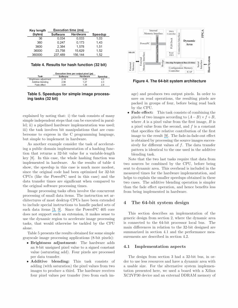
Table 4. Results for hash function (32 bit)
Table 5. Speedups for simple image process-
ing tasks (32 bit)
explained by noting that: i) the task consists of manysimple independent steps that can be executed in paral-lel; ii) a pipelined hardware implementation was used;iii) the task involves bit manipulations that are cum-bersome to express in the C programming language,but simple to implement in hardware.
As another example consider the task of accelerat-ing a public domain implementation of a hashing func-tion that returns a 32-bit value for a variable-lengthkey [8]. In this case, the whole hashing function wasimplemented in hardware. As the results of table 4show, the speedup in this case is much more modest,since the original code had been optimized for 32-bitCPUs (like the PowerPC used in this case) and thedata transfer times are significant when compared tothe original software processing times.
Image processing tasks often involve the concurrentprocessing of small data items. The instruction set ar-chitectures of most desktop CPUs have been extendedto include special instructions to handle packed sets ofsuch data items [3, 9]. Since the PowerPC 405 coredoes not support such an extension, it makes sense touse the dynamic region to accelerate image processingtasks, that would otherwise be tackled by the CPUalone.
Table 5 presents the results obtained for some simplegrayscale image processing applications (8-bit pixels):
• Brightness adjustment: The hardware addsan 8-bit unsigned pixel value to a signed constantvalue (saturating add). Four pixels are processedper data transfer.
• Additive blending: This task consists ofadding (with saturation) the pixel values from twoimages to produce a third. The hardware receivesfour pixel values per transfer (two from each im-
Figure 4. The 64-bit system architecture
age) and produces two output pixels. In order tosave on read operations, the resulting pixels arepacked in groups of four, before being read backby the CPU.
• Fade effect: This task consists of combining thepixels of two images according to (A−B)×f +B,where A is a pixel value from the first image, B isa pixel value from the second, and f is a constantthat specifies the relative contribution of the firstimage to the result [9]. The fade-in-fade-out effectis obtained by processing the source images succes-sively for different values of f . The data transferpattern is identical to the one used in the additiveblending task.
Note that the two last tasks require that data fromtwo sources be combined by the CPU, before beingsent to dynamic area. This overhead is included in themeasured times for the hardware implementation, andhelps to explain the smaller speedups obtained in thesetwo cases. The additive blending operation is simplerthan the fade effect operation, and hence benefits lessfrom being implemented in hardware.
4 The 64-bit system design
This section describes an implementation of thegeneric design from section 2, where the dynamic areais connected to the 64-bit processor local bus. Themain differences in relation to the 32-bit designed aresummarized in section 4.1 and the performance mea-surements are described in section 4.2.
4.1 Implementation aspects
The design from section 3 had a 32-bit bus, in or-der to use less resources and have a dynamic area witha usable size. For the alternative system implemen-tation presented here, we used a board with a XilinxXC2VP30 device and an external DDRAM memory of
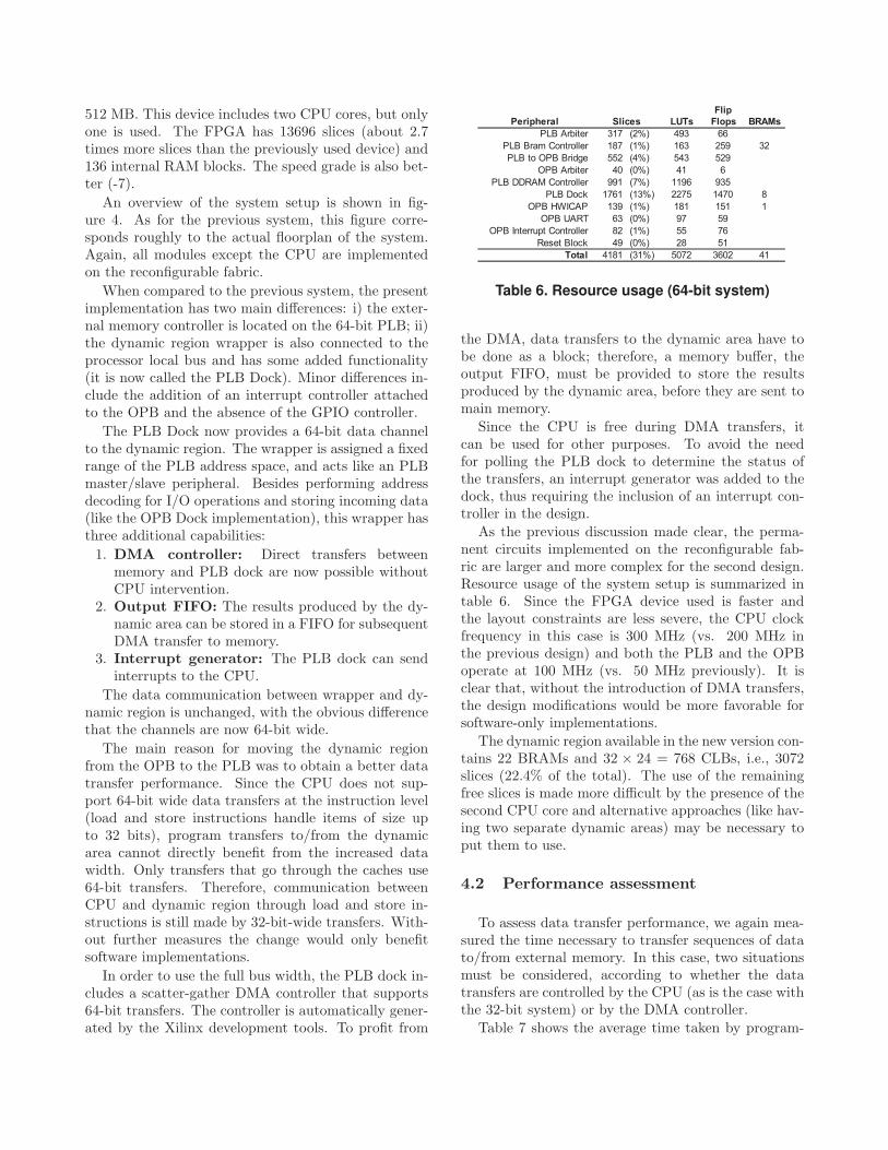
512 MB. This device includes two CPU cores, but onlyone is used. The FPGA has 13696 slices (about 2.7times more slices than the previously used device) and136 internal RAM blocks. The speed grade is also bet-ter (-7).
An overview of the system setup is shown in fig-ure 4. As for the previous system, this figure corre-sponds roughly to the actual floorplan of the system.Again, all modules except the CPU are implementedon the reconfigurable fabric.
When compared to the previous system, the presentimplementation has two main differences: i) the exter-nal memory controller is located on the 64-bit PLB; ii)the dynamic region wrapper is also connected to theprocessor local bus and has some added functionality(it is now called the PLB Dock). Minor differences in-clude the addition of an interrupt controller attachedto the OPB and the absence of the GPIO controller.
The PLB Dock now provides a 64-bit data channelto the dynamic region. The wrapper is assigned a fixedrange of the PLB address space, and acts like an PLBmaster/slave peripheral. Besides performing addressdecoding for I/O operations and storing incoming data(like the OPB Dock implementation), this wrapper hasthree additional capabilities:
1. DMA controller: Direct transfers betweenmemory and PLB dock are now possible withoutCPU intervention.
2. Output FIFO: The results produced by the dy-namic area can be stored in a FIFO for subsequentDMA transfer to memory.
3. Interrupt generator: The PLB dock can sendinterrupts to the CPU.
The data communication between wrapper and dy-namic region is unchanged, with the obvious differencethat the channels are now 64-bit wide.
The main reason for moving the dynamic regionfrom the OPB to the PLB was to obtain a better datatransfer performance. Since the CPU does not sup-port 64-bit wide data transfers at the instruction level(load and store instructions handle items of size upto 32 bits), program transfers to/from the dynamicarea cannot directly benefit from the increased datawidth. Only transfers that go through the caches use64-bit transfers. Therefore, communication betweenCPU and dynamic region through load and store in-structions is still made by 32-bit-wide transfers. With-out further measures the change would only benefitsoftware implementations.
In order to use the full bus width, the PLB dock in-cludes a scatter-gather DMA controller that supports64-bit transfers. The controller is automatically gener-ated by the Xilinx development tools. To profit from
Table 6. Resource usage (64-bit system)
the DMA, data transfers to the dynamic area have tobe done as a block; therefore, a memory buffer, theoutput FIFO, must be provided to store the resultsproduced by the dynamic area, before they are sent tomain memory.
Since the CPU is free during DMA transfers, itcan be used for other purposes. To avoid the needfor polling the PLB dock to determine the status ofthe transfers, an interrupt generator was added to thedock, thus requiring the inclusion of an interrupt con-troller in the design.
As the previous discussion made clear, the perma-nent circuits implemented on the reconfigurable fab-ric are larger and more complex for the second design.Resource usage of the system setup is summarized intable 6. Since the FPGA device used is faster andthe layout constraints are less severe, the CPU clockfrequency in this case is 300 MHz (vs. 200 MHz inthe previous design) and both the PLB and the OPBoperate at 100 MHz (vs. 50 MHz previously). It isclear that, without the introduction of DMA transfers,the design modifications would be more favorable forsoftware-only implementations.
The dynamic region available in the new version con-tains 22 BRAMs and 32 × 24 = 768 CLBs, i.e., 3072slices (22.4% of the total). The use of the remainingfree slices is made more difficult by the presence of thesecond CPU core and alternative approaches (like hav-ing two separate dynamic areas) may be necessary toput them to use.
4.2 Performance assessment
To assess data transfer performance, we again mea-sured the time necessary to transfer sequences of datato/from external memory. In this case, two situationsmust be considered, according to whether the datatransfers are controlled by the CPU (as is the case withthe 32-bit system) or by the DMA controller.
Table 7 shows the average time taken by program-

Table 7. Measured times for 32-bit data trans-fers between dynamic region and external
memory (CPU controlled)
Table 8. Measured times for 64-bit data trans-
fers between dynamic region and externalmemory (DMA-controlled)
controlled transfers: sequences of write operations, se-quences of read operations and sequences of interleavedwrite/read operations. In this case, each transfer in-volves a 32-bit value (as discussed previously). Thisoperation is the same as the one performed in the 32-bit system and direct comparison of the values is le-gitimate. A decrease in transfer time between 4 and6 times, depending on the transfer type, can be ob-served. Part of this decrease is due to improved busspeed (a factor of 2) and CPU frequency (a factor of1.5). The additional improvement presumably comesfrom the fact that no PLB-to-OPB bridge is used.
Table 8 shows the average time per transfer whenusing DMA. In this method, each transfer involves a64-bit value, using the data path to the fullest. The in-terleaved write/read operations are block-interleaved:the output data is stored in the output FIFO, while thewrite operation is being performed; when the FIFO be-comes full, the write operation stops and the data con-tained in the FIFO is transferred the external memoryby a DMA operation. These operations are repeated,until all the data is transferred. The current outputFIFO stores up to 2047 64-bit values.
The times reported in tables 7 and 8 allow the devel-oper to determine a lower bound for the time requiredto use the dynamic area with different transfer meth-
Table 9. Results for pattern matching in bi-nary images (64 bit).
Table 10. Results for a hash function imple-mentation (64 bit)
ods and different data widths. This lower bound can beused to make a first assessment of the improvements,that can be obtained by moving a function from soft-ware to hardware, and to evaluate the gains from usingeach of the two data transfers methods.
We took our first two implementation examples fromthe 32-bit system, and transferred them on the newsystem without any modifications: the data transfersdon’t take advantage of the 64-bit bus width and arecontrolled by the CPU. Tables 9 and 10 present theresults. Both tasks benefit greatly from the new sys-tem and both software and hardware implementationsperform considerably better.
In general, the results follow the trends observedfor the transfer times, as expected. In the patternmatching task, a decrease in the hardware vs. softwarespeedup is obtained, because the software implementa-tion benefited more from the quicker access to memory.The hardware implementations still maintain a consid-erable performance advantage. The hash value calcu-lation task, on the other hand, shows only a slightlybetter speedup for the hardware implementation.
We also tested the system with the more demand-ing hash function SHA1 [4]. This hashing algorithmis geared towards 32-bit implementations. Our imple-mentation does not fit into the dynamic area of the32-bit system, so no comparison can be done. The re-sults of table 11 show a considerable performance gainfor the hardware implementation (using 32-bit CPU-controlled data transfers). The software implementa-tion (taken from the RFC document) has a large over-

Table 11. Results for SHA-1 implementation
Table 12. Results for simple image process-ing tasks (64 bit)
head for smaller data sets. The overhead’s relative im-portance decreases for larger data sets.
A 64-bit DMA-controlled implementation of the im-age processing tasks presented in section 3.2 was alsomade. The results are shown in table 12. For the firsttask, there is a clear increase of the speedup obtainedby the hardware (on top of the increased performanceof the software version). The reason for this is that the64-bit data transfers could be employed without addi-tional work, since only one image is involved. The othertasks show a significantly smaller speedup increase, be-cause the data of the two source images had to be com-bined by the CPU, before being sent to the dynamicarea. This time overhead appears in the table under theheading of “data preparation”, and is directly attribut-able to the constraints of the DMA transfer mode.
5 Conclusion
The paper discusses several issues, that arise whentrying to exploit effectively the run-time reconfigura-tion capabilities of platform FPGAs. Two implemen-tations of the same general approach are presented, andcompared with the help of several small studies. The is-sues associated with data transfers between embeddedCPU and dynamically reconfigured circuits are shownto contribute significantly to overall performance.
For the systems considered in this work, the use of64-bit data transfers is hampered by the fact that theCPU does not support programmatic 64-bit data trans-fers; only transfers that go through the caches profitfrom the higher bus width. In order to use the 64-bitbus width effectively to communicate with the dynamicarea, it is necessary to employ DMA transfers. These,
however, pose significant restrictions on data organiza-tion and access patterns, making the adaptation of thesoftware-based algorithms more difficult and time con-suming. When the difficulties can be overcome, signif-icantly better performance can be achieved. It is alsoimportant to note that the changes from the first tothe second system affect hardware and software in adifferent manner, so the relative merits of using a puresoftware approach vs. a combined hardware/softwaresolution also change.
References
[1] B. Blodget, C. Bobda, M. Hubner, and A. Niy-onkuru. Partial and dynamically reconfiguration ofXilinx Virtex-II FPGAs. In Proceedings FPL’04, pages801–810, 2004.
[2] E. Carvalho, N. Calazans, E. Briao, and F. Moraes.PaDReH: a framework for the design and implemen-tation of dynamically and partially reconfigurable sys-tems. In Proceedings SBCCI’04, pages 10–15, 2004.
[3] K. Diefendorff, P. Dubey, R. Hochsprung, andH. Scale. AltiVec extension to PowerPC acceleratesmedia processing. IEEE Micro, 20(2):85–95, 2000.
[4] D. Eastlake and P. Jones. RFC 3174 — US SecureHash Algorithm 1 (SHA1). RFC Editor, Sept. 2001.
[5] J. C. Ferreira and M. M. Silva. Run-time reconfigura-tion support for FPGAs with embedded CPUs: Thehardware layer. In Proceedings RAW’05, Denver, Col-orado, Apr. 2005.
[6] E. L. Horta, J. W. Lockwood, and S. T. Kofuji. UsingPARBIT to implement partial run-time reconfigurablesystems. In Proceedings FPL’02, pages 182–191, Lon-don, UK, 2002. Springer-Verlag.
[7] IBM. The CoreConnect bus architecture, Sept. 1999.[8] B. Jenkins. Hash functions. Dr. Dobb’s Journal,
22(9):107–109, Sept. 1997.[9] A. Peleg, S. Wilkie, and U. Weiser. Intel MMX for
multimedia PCs. Commun. ACM, 40(1):24–38, 1997.[10] A. K. Raghavan and P. Sutton. JPG–a partial bit-
stream generation tool to support partial reconfigu-ration in Virtex FPGAs. In Proceedings IPDPS’02,page 192, Washington, DC, USA, 2002. IEEE Com-puter Society.
[11] P. Sedcole, B. Blodget, J. Anderson, P. Lysaght, andT. Becker. Modular partial reconfiguration in VirtexFPGAS. In Proceedings FPL’05, pages 211–216, 2005.
[12] M. L. Silva and J. C. Ferreira. Generation ofhardware modules for run-time reconfigurable hybridCPU/FPGA systems. In Proceedings DCIS’05, Lis-boa, Portugal, Nov. 2005.
[13] M. Ullmann, M. Hubner, B. Grimm, and J. Becker.An FPGA run-time system for dynamical on-demandreconfiguration. In IPDPS’04, page 135a. IEEE Com-puter Society, 2004.
[14] Xilinx. Two flows for partial reconfiguration: Modulebase or small bit manipulations. Application note 290,Sept. 2004.