
Contrasting topologies for regular interconnection networks under the constraints of nanoscale...
6
Contrasting Topologies for Regular Interconnection Networks under the Constraints of Nanoscale Silicon Technology Daniele Ludovici, Georgi N. Gaydadjiev Computer Engineering Lab., TUDelft 2628 CD Delft, The Netherlands Francisco Gilabert, Maria E. Gomez GAP, University of Valencia Davide Bertozzi ENDIF, University of Ferrara 44100 Ferrara, Italy ABSTRACT Nowadays, system designers have adopted Networks-on-Chip as communication infrastructure of general-purpose tile-based Multi-Processor System-on-Chip (MPSoC). Such decision im- plies that a certain topology has to be selected to efficiently interconnect many cores on the chip. To ease such a choice, the networking literature offers a plethora of works about topology analysis and characterization for the off-chip do- main. However, theoretical parameters and many intuitive assumptions of such off-chip networks do not necessarily hold when a topology is laid out on a 2D silicon surface. This is due to the distinctive features of silicon technology design pitfalls. This work is a first milestone to bridge this gap, in fact, we propose a comprehensive analysis framework to as- sess k-ary n-mesh and C-mesh topologies at different level of abstractions, from system to layout level, while capturing implications of system and layout parameters across design hierarchy. When a certain topology proves to be slow due to long links crossing the chip, pipeline stages have been in- serted to cope with such slow-down. Furthermore, costs of such speed-up technique have been evaluated to draw a com- prehensive performance/area figure. Categories and Subject Descriptors B.7.1 [Hardware]: Integrated Circuits—VLSI General Terms Design, Performance Keywords System-on-Chip integration, Network topologies, Link design techniques, Network-on-Chip The gap between the constraints driving the design of on- chip vs. off-chip interconnection networks (and hence the gap between the final network architectures selected for use in each domain) is increasingly widening even more as an effect of the relentless pace of technology scaling to the nanoscale regime. New physical effects come into play and may either degrade performance/power in an unpredictable way or even affect feasibility of the design at hand or of specific architecture design techniques. Permission to make digital or hard copies of all or part of this work for personal or classroom use is granted without fee provided that copies are not made or distributed for profit or commercial advantage and that copies bear this notice and the full citation on the first page. To copy otherwise, to republish, to post on servers or to redistribute to lists, requires prior specific permission and/or a fee. NoCArc ’10, December 4, 2010, Atlanta, Georgia, USA Copyright 2010 ACM ...$10.00. Examples concern the large buffering cost associated with techniques borrowed from the off-chip domain (e.g., for con- gestion management strategies or for deadlock-free and multi- cast friendly switching mechanisms) which are not affordable in the on-chip domain. Moreover, the interconnect reverse scaling is making designs for on-chip integration increasingly interconnect-dominated, due to the delay associated with the shrinking cross-section area of on-chip interconnects. This effect becomes increasingly severe at each technology node and tends to widen the gap between post-synthesis and post- place&route performance figures and even to move critical path delays from logic blocks to large global wires. Selection of the topology connectivity pattern in the early stages of network design is a decision which is extremely sen- sitive to both the effects illustrated above. In fact, topologies for on-chip networks must match the 2D silicon surface, while off-chip realizations are dictated by board/rack organization. The 2D mapping constraint raises implementation issues such as wire crossings, wires of uneven length or the decrease of switch operating frequency with the number of I/O ports. As an ultimate consequence, topologies borrowed from off-chip networks should be reassessed in the on-chip environment and validated against the design pitfalls in this domain. This is the motivation that lies at the core of this paper. We are aware that many regular topologies feature better ab- stract properties (e.g., diameter, bisection bandwidth) than a 2D mesh, however their implementation in an on-chip setting is very challenging. The objective of this paper is to quantify to which extent their inherently better abstract properties is impacted by the degradation effects of the physical synthe- sis on nanoscale silicon technologies. Proving whether these topologies are still efficient (or even feasible) after the physical degradation mechanisms is a non-intuitive task. This paper takes on this challenge. Previous work in the open litera- ture features frameworks able to evaluate network topologies only from a pure theoretical viewpoint thus neglecting all the physical effects of nanoscale technologies. On the other hand, other works focused on the physical modeling of interconnec- tion networks but only limited to small scale systems mainly due to the unaffordable time and memory requirements for the synthesis of such systems. Therefore, our contribution consists of: • an area and network critical path modeling framework able to accurately analyze performance of k-ary n-mesh and C-mesh topologies with layout awareness. Our pro- posed methodology scales easily to large size systems as only a few sub-systems of the whole network need to be analyze to draw comprehensive area and performance figures. When accounting for layout effects, conclusions drawn from high-level theoretical analysis can be highly misleading. Moreover, k-ary n-mesh and C-mesh topologies suffer of a considerable slow down when laid out on silicon. This is mainly due to their long links which represent the speed bot- tleneck of the whole network. To tackle this problem, pipeline stages are typically implemented in links of the top dimen- sions. To the best of our knowledge, all the previously pub- NoCArc 2010 — December 4, 2010, Georgia, Atlanta, USA 37
Transcript of Contrasting topologies for regular interconnection networks under the constraints of nanoscale...
Contrasting Topologies for Regular InterconnectionNetworks under the Constraintsof Nanoscale Silicon Technology
Daniele Ludovici, Georgi N. GaydadjievComputer Engineering Lab., TUDelft
2628 CD Delft, The Netherlands
Francisco Gilabert,Maria E. Gomez
GAP, University of Valencia
Davide BertozziENDIF, University of Ferrara
44100 Ferrara, Italy
ABSTRACTNowadays, system designers have adopted Networks-on-Chipas communication infrastructure of general-purpose tile-basedMulti-Processor System-on-Chip (MPSoC). Such decision im-plies that a certain topology has to be selected to efficientlyinterconnect many cores on the chip. To ease such a choice,the networking literature offers a plethora of works abouttopology analysis and characterization for the off-chip do-main. However, theoretical parameters and many intuitiveassumptions of such off-chip networks do not necessarily holdwhen a topology is laid out on a 2D silicon surface. Thisis due to the distinctive features of silicon technology designpitfalls. This work is a first milestone to bridge this gap, infact, we propose a comprehensive analysis framework to as-sess k-ary n-mesh and C-mesh topologies at different levelof abstractions, from system to layout level, while capturingimplications of system and layout parameters across designhierarchy. When a certain topology proves to be slow dueto long links crossing the chip, pipeline stages have been in-serted to cope with such slow-down. Furthermore, costs ofsuch speed-up technique have been evaluated to draw a com-prehensive performance/area figure.
Categories and Subject DescriptorsB.7.1 [Hardware]: Integrated Circuits—VLSI
General TermsDesign, Performance
KeywordsSystem-on-Chip integration, Network topologies, Link designtechniques, Network-on-Chip
The gap between the constraints driving the design of on-chip vs. off-chip interconnection networks (and hence the gapbetween the final network architectures selected for use in eachdomain) is increasingly widening even more as an effect of therelentless pace of technology scaling to the nanoscale regime.New physical effects come into play and may either degradeperformance/power in an unpredictable way or even affectfeasibility of the design at hand or of specific architecturedesign techniques.
Permission to make digital or hard copies of all or part of this work forpersonal or classroom use is granted without fee provided that copies arenot made or distributed for profit or commercial advantage and that copiesbear this notice and the full citation on the first page. To copy otherwise, torepublish, to post on servers or to redistribute to lists, requires prior specificpermission and/or a fee.NoCArc ’10, December 4, 2010, Atlanta, Georgia, USACopyright 2010 ACM ...$10.00.
Examples concern the large buffering cost associated withtechniques borrowed from the off-chip domain (e.g., for con-gestion management strategies or for deadlock-free and multi-cast friendly switching mechanisms) which are not affordablein the on-chip domain. Moreover, the interconnect reversescaling is making designs for on-chip integration increasinglyinterconnect-dominated, due to the delay associated with theshrinking cross-section area of on-chip interconnects. Thiseffect becomes increasingly severe at each technology nodeand tends to widen the gap between post-synthesis and post-place&route performance figures and even to move criticalpath delays from logic blocks to large global wires.
Selection of the topology connectivity pattern in the earlystages of network design is a decision which is extremely sen-sitive to both the effects illustrated above. In fact, topologiesfor on-chip networks must match the 2D silicon surface, whileoff-chip realizations are dictated by board/rack organization.The 2D mapping constraint raises implementation issues suchas wire crossings, wires of uneven length or the decrease ofswitch operating frequency with the number of I/O ports. Asan ultimate consequence, topologies borrowed from off-chipnetworks should be reassessed in the on-chip environment andvalidated against the design pitfalls in this domain.
This is the motivation that lies at the core of this paper.We are aware that many regular topologies feature better ab-stract properties (e.g., diameter, bisection bandwidth) than a2D mesh, however their implementation in an on-chip settingis very challenging. The objective of this paper is to quantifyto which extent their inherently better abstract properties isimpacted by the degradation effects of the physical synthe-sis on nanoscale silicon technologies. Proving whether thesetopologies are still efficient (or even feasible) after the physicaldegradation mechanisms is a non-intuitive task. This papertakes on this challenge. Previous work in the open litera-ture features frameworks able to evaluate network topologiesonly from a pure theoretical viewpoint thus neglecting all thephysical effects of nanoscale technologies. On the other hand,other works focused on the physical modeling of interconnec-tion networks but only limited to small scale systems mainlydue to the unaffordable time and memory requirements forthe synthesis of such systems.Therefore, our contribution consists of:
• an area and network critical path modeling frameworkable to accurately analyze performance of k-ary n-meshand C-mesh topologies with layout awareness. Our pro-posed methodology scales easily to large size systems asonly a few sub-systems of the whole network need to beanalyze to draw comprehensive area and performancefigures.
When accounting for layout effects, conclusions drawn fromhigh-level theoretical analysis can be highly misleading.Moreover, k-ary n-mesh and C-mesh topologies suffer of aconsiderable slow down when laid out on silicon. This ismainly due to their long links which represent the speed bot-tleneck of the whole network. To tackle this problem, pipelinestages are typically implemented in links of the top dimen-sions. To the best of our knowledge, all the previously pub-
NoCArc 2010 — December 4, 2010, Georgia, Atlanta, USA 37
lished analysis frameworks do not take into account the impli-cations of utilizing such technique from an area/timing view-point with layout awareness.Therefore, the second contribution is:
• the enhancement of our modeling framework with thecapability of accurately capture the impact of using linkpipelining from both the area and timing point of viewaccounting for physical effects. Interestingly, when con-sidering also such layout implications of link pipeliningutilization, some topologies previously considered lowspeed turn out to be competitive.
Last contribution can be summarized as follows:
• our previous work only considered systems with k-ary n-mesh where cores and network speed was constrained byan integer divider thus limiting the overall performanceof the system. In this work, we extended our analysis tosystems implemented as globally asynchronous locallysynchronous (GALS) system where cores and networkspeed ratio can be any. Interestingly, the adoption ofa GALS approach has considerable consequences on theperformance/area figures of various topologies that werenot competitive at all in the previously investigated sce-narios. In order to achieve this objective, our transac-tion level simulator has been enhanced with dual-clockFIFO interfaces for cores and network frequency decou-pling.
The remainder of this paper is organized as follows. Section1 reviews previous work regarding topology mapping for NoCsystems. Section 3 describes the modeling methodology uti-lized to characterize the topologies under analysis. Physicallayout results of such section are utilized in Section 4 to carryout a system-level exploration with layout awareness. Finally,conclusions are drawn in Section 5.
1. RELATED WORKAlthough it has been widely used across a number of
Network-on-Chip tile-based embedded and high performancemicroprocessors designs [9, 10], the 2D-mesh NoC topologyfeatures well-known drawbacks in the communication latencyscalability and concentration of the traffic in the center ofthe network[6]. This has motivated works in the open lit-erature that come up with optimized NoC topologies whilekeeping regularity properties as much as possible. A novelinterconnect topology called spidergon was proposed in [21],where each core is connected to the clockwise, counterclock-wise and diagonal node. A traditional wormhole-routed meshaugmented by a hierarchical ring interconnect for routingglobal traffic is illustrated in [11]. NOVA is a hybrid inter-connect topology targeted at FPGA and is compared in [12]with star, torus and hypercube topologies. Gilabert et al.propose in [13] to use high-dimensional topologies, using dif-ferent metal layers to reduce long link delay and trading-offdimensions with the number of cores per router. However,this is not backed by any physical synthesis run. The work in[6] proposes a concentrated mesh architecture with replicatedsubnetworks and express channels.
Topology exploration is an active research area due to thelarge scale of on-chip networks and to the feasibility challengesposed by nanoscale technologies [14, 16, 17]. Unfortunately, astechnology scales to the nanometer regime, topology analysisand exploration needs to be performed with novel method-ologies and tools that account for the effects of nanoscalephysics, largely impacting final performance and even feasi-bility of many NoC topologies. A general guideline drivingnetwork-on-chip (NoC) design under severe technology con-straints consists of silicon-aware decision-making at each hi-erarchical level [18]. This is likely to result in less designre-spins and in faster timing closure. In this direction, newtools are emerging that guide designers towards a subset ofmost suitable candidates for on-chip network designs whileconsidering the complex trade-offs between applications, ar-chitectures and technologies [19, 20].
Our previous work in [2, 3, 5] presented silicon-aware topol-ogy analysis and comparison for networks with 16 nodes. Inall these works, the exploration of the design space is per-formed through a transaction-level simulation environmentthat is able to back-annotate key parameters (frequency, la-tency, area) from the results of physical synthesis. When ex-tending the analysis to larger 64-tile networks, the unafford-able time and memory requirements for the synthesis of suchsystems makes a comprehensive exploration based on post-layout figures unfeasible. This is the reason why our previouswork was limited only to 16-tile systems. In order to ex-tend the exploration to larger 64-tile networks, in this workwe devise (i) a novel modeling methodology based on selec-tive synthesis runs that is able to capture the key post-layoutparameters of a large scale topology such as, maximum fre-quency and switch cell area. (ii) Moreover, our framework isable to capture the impact of link buffering and link pipeliningfrom the timing and area cost viewpoint. (iii) Furthermore,by utilizing such physical parameters in our transaction-levelsimulator, we are able to perform a layout-aware system-levelanalysis. This way, overall area and performance figures canbe drawn. Differently from our previous work in [2], the sim-ulator has been enhanced with the implementation of dual-clock FIFO interfaces thus enabling the modeling of systemswhere cores and network are completely decoupled from thefrequency viewpoint. Interestingly, achieved results may lookcounterintuitive at a first glance when compared with com-monly known theoretical properties of the investigated topolo-gies.
Next section will describe such abstract properties whichwill be later on put in discussion by the physical implemen-tation part of this work.
2. HIGH-LEVEL TOPOLOGY EXPLO-RATION
In this section a high-level comparison of topology perfor-mance is provided. However, this analysis will only give thehigh-level perspective and is agnostic of physical implementa-tion effects. Nonetheless, it may be used in the early stagesof system design to select the subset of the most promisingtopology candidates.
We restrict our focus to large 64-tile systems. The numberof cores attached to each switch has been limited to four as ahigher number of connected cores would introduce serious per-formance and feasibility issues. In fact, the topology wouldhave a very low bisection bandwidth. Moreover, the place-ment of cores around the switches would not be a trivial tasksince the length of the injection/ejection links would increase.This would significantly limit overall NoC performance [3].
Table 1 summarizes the values of the properties of all 64cores configurations considered for each topology. The anal-ysis includes two different configurations of the CMesh net-work. From a pure topology viewpoint, a CMesh can be seenas a classical 2-D mesh with express links, regardless of thenumber of cores attached to each switch. As the investigatedsystems sizes are quite large, several topology configurationsare possible and need to be taken into account. The best solu-tion for high traffic loads is represented by the 2-ary 6-mesh.Moreover, this topology has one of the lowest hop counts (6),thus making it well suited for latency sensitive systems andapplications. However, it requires the highest amount of re-sources: 64 switches of degree 7 and 384 unidirectional links.On the other hand, from a low-latency viewpoint, the best so-lution is either the 2-ary 4-mesh or the 4-cmesh, which againare completely equivalent from a high-level view-point.
Overall, the best topology would be the 2-ary 6-mesh, asit provides four time more bisection bandwidth than the low-latency solutions, while requiring only two hops more (6 hopsin the 2-ary 6-mesh versus 4 hops in both low-latency solu-tions). The only drawback of such topology lies in the highnumber of required resources. Finally, when system specifi-cations do not require such a high bisection bandwidth, the2-ary 5-mesh solution becomes a good trade-off that providestwice the bisection bandwidth of the low-latency solutions(while increasing the number of hops by one). Clearly, by
NoCArc 2010 — December 4, 2010, Georgia, Atlanta, USA 38
Topology Switches Cores/ Max. Unidir. Bisection Hop Connect.switch degree links bandwidth count
8-ary 2-mesh 64 1 5 224 16 14 24-ary 3-mesh 64 1 7 288 32 9 34-ary 2-mesh 16 4 8 48 8 6 22-ary 6-mesh 64 1 7 384 64 6 62-ary 5-mesh 32 2 7 160 32 5 52-ary 4-mesh 16 4 8 64 16 4 4
8-cmesh 64 1 5 256 32 8 44-cmesh 16 4 8 64 16 4 4
Table 1: High level parameters of topologies with 64-tile.
blindly relying on this table and upon the underlying theo-retical analysis, a designer would easily discard the 2D mesh(8-ary 2-mesh) as candidate topology.
The remainder of this paper will prove that theoreticalproperties of such topologies are put in discussions when lay-out considerations are taken into account and may even leadto counterintuitive final results.
Next section will present the characterization methodologythat is at the core of our modeling framework. Such method-ology will be used to extrapolate key physical parameters tobe back-annotated in the transaction-level simulator, thus en-abling a layout-aware system-level exploration.
3. PHYSICAL MODELING FRAMEWORKThe xpipesLite [8] switch was used as the basic building
block to construct the 64-tile topologies under test. However,exploring the design space of topologies with such a largenumber of cores with full physical synthesis proved impracti-cal due to synthesis time and memory capacity requirements.Therefore, next section will present a way to cut down on thenumber of physical synthesis tests while still characterizingthe full topology with high accuracy.
All the analyzed topologies of this work have been laid outby means of a backend synthesis flow leveraging industrialtools. The topology specification is fed to the xpipescompilertool[22], resulting in the generation of self-contained SystemCcode for RTL-equivalent simulation and for synthesis. Syn-opsys Physical Compiler is used for placement-aware logicsynthesis. The technology library is a low-power low-Vth65nm STMicroelectronics library available through the CMPproject [7]. Placement and routing have been performed withCadence SoC Encounter.
3.1 Characterization MethodologyIn order to accurately characterize the switch and link
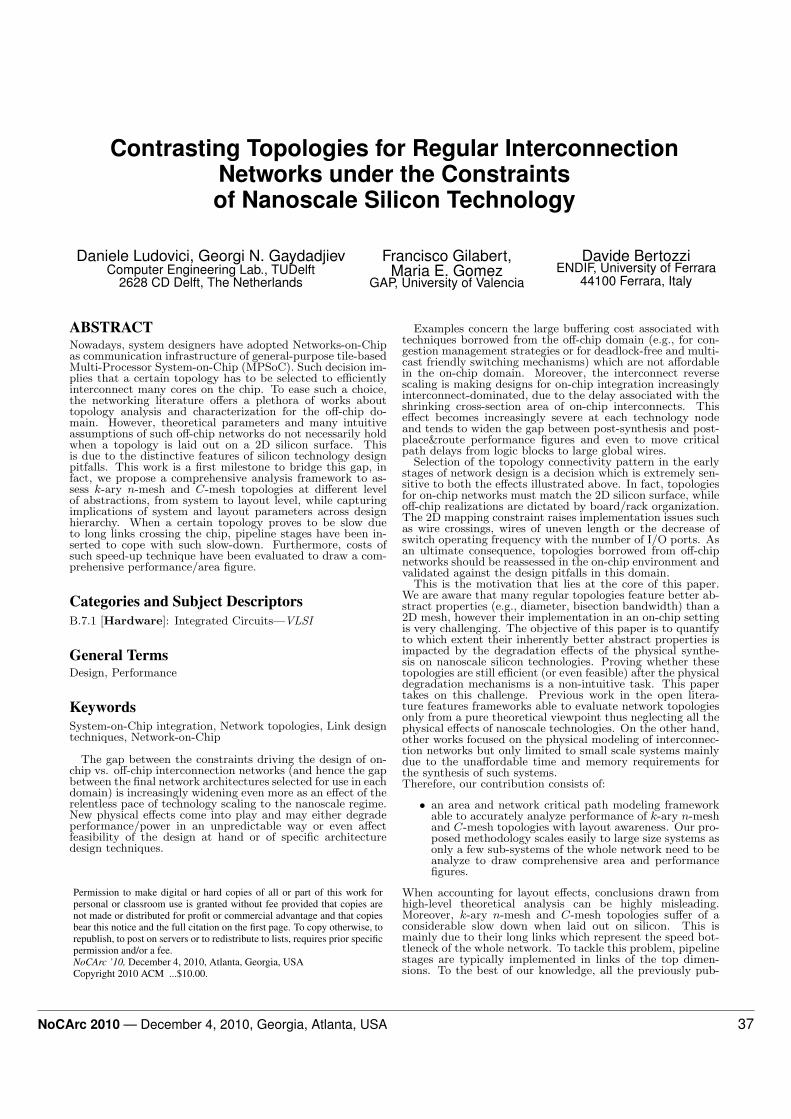
buffering cell area of the topology under analysis, we pro-pose to utilize the methodology depicted in Figure 1. In fact,as already reported in our previous work [2, 3, 5], the perfor-mance bottleneck of a topology lies in its longest switch–to–switch communication channel. Aware of this, from a high-level topology specification we build a sub-system composedof two communicating switches at the maximum possible dis-tance in the topology. This way, the critical link delay canbe extracted. Such delay (which is the critical path delay ofthe network) is then used as the target delay to re-synthesize,place and route all the possible switch–to–switch sub-systemsfor each different inter-switch link length. The reason forthis is that our goal is to accurately capture the switch cellarea at a certain distance and at a certain target speed. Itis well known from logic synthesis theory that as the targetspeed is decreased, large area can be saved. In this direction,it would make no sense to synthesize switches for maximumperformance when a long link limits overall network speed(unless decoupling techniques like link pipelining are used, aswe will see later on). Please note that each switch of the builtsub-system has been pre-characterized standalone with theinput/output delay that is able to tolerate from its neighborcommunicating block. These parameters were set in such away that the communication link delay is optimized as muchas possible thus shortening the critical path of the switch–to–switch modeling architecture.
critical link delay
accurate switch cell area
topology specification
switch−to−switch sub−system
at maximum link distance
extract
accurate switch and linkbuffering cell area
all possible switch−to−switch
inter−switch link length
sub−system for each different
topology specification
critical link delay
extract
build
re−synthesis
Figure 1: Characterization methodology flow.
With this methodology, only a few selected synthesis runsfor each topology need to be performed to characterize itsdelay and area as a whole. The approximation lies in theavailability of enough routing channels for regular routing ofNoC links and in the balance preservation of relative wiredelays in links that undergo bending in the actual layout.
Moreover, with this method we are also able to capture thelink buffering cost, in fact, by leveraging the report of theutilized physical synthesis tool, we are able to trace the in-ferred buffers of the switch–to–switch channel. In order to beas accurate as possible when characterizing a topology, twocommunicating ports of both switches in our subsystem wereleft unconnected. They are the ports connecting to the pro-cessing cores, which are typically placed close to their switchand therefore feature minimum capacitive load. Should we failto model this (even by simply leaving an output port uncon-nected), the input and output buffer of the switch would beincorrectly sized by the synthesis tools by using larger drivingstrengths than actually needed for the switch–to–core links.
A further step of our work is the estimation of the numberof required pipeline stages for each link to speed up a topol-ogy. For this purpose, such retiming stages are instantiatedalong the communication link thus breaking the switch–to–switch critical path. By incrementing the number of pipelinestages, we were able to achieve timing closure bringing backthe critical path to the second link dimension. In fact, asmentioned later, in order to limit area overhead, our pipelinestage insertion criteria consisted of adding such stages onlyfrom the third link dimension onwards.
The next section starts by commenting physical synthesisresults achieved for 64-tile topologies without link pipelin-ing. Consequently, the analysis is shifted to pipelined sys-tems. Section 4 will utilize the obtained physical results tocarry out a system-level exploration with layout-awareness.
NoCArc 2010 — December 4, 2010, Georgia, Atlanta, USA 39
3.2 64-tile topologiesAs reported in Table 2, the range of possible switch radix
per topology spans from a reasonable 6 to a large 12 thatis even more difficult to place and route as a stand-aloneblock without DRC (design rules check) violations [4]. Post-synthesis frequency results reflect the increasing trend withthe switch radix, in agreement with the analysis of [4]. Af-ter placement and routing, the effect of the long links comesnoticeably into play. Most of the topologies suffer from longswitch–to–switch channels that need to be routed along thechip. For the sake of the analysis, only the longest link pertopology is reported in the 5th column. By comparing suchcolumn with the 4th one, it is possible to recognize a clear cor-relation between the increasing link length and the decreasingoperating speed of the topology under analysis. In fact, thecritical role of the interconnect is a major factor limiting theperformance of a topology. It should also be observed thatalso some logic gates end up in series to the critical links closeto the far-ends. They are associated with flow control man-agement and further contribute to the critical path delay. Thetrend above is even more apparent when we consider largertopologies. In fact, only topologies with short links (e.g., 8-ary2-mesh and 4-ary 2-mesh) can work at a reasonable frequencyfor realistic application scenarios.
TOPOLOGY Radix post-synthesis post-P&R longest linkfrequency frequency
8-ary 2-mesh 6 1.08GHz 890MHz 1.5mm8-cmesh 6 1.08GHz 250MHz 6.75mm
4-ary 3-mesh 8 950Mhz 220MHz 6.9mm2-ary 6-mesh 8 950Mhz 220MHz 6.9mm2-ary 5-mesh 9 810MHz 230MHz 6.96mm4-ary 2-mesh 12 720MHz 530MHz 3.0mm2-ary 4-mesh 12 720MHz 260MHz 6.4mm
4-cmesh 12 720MHz 260MHz 6.4mm
Table 2: Post-place&route results of the 64-tiletopologies under test.
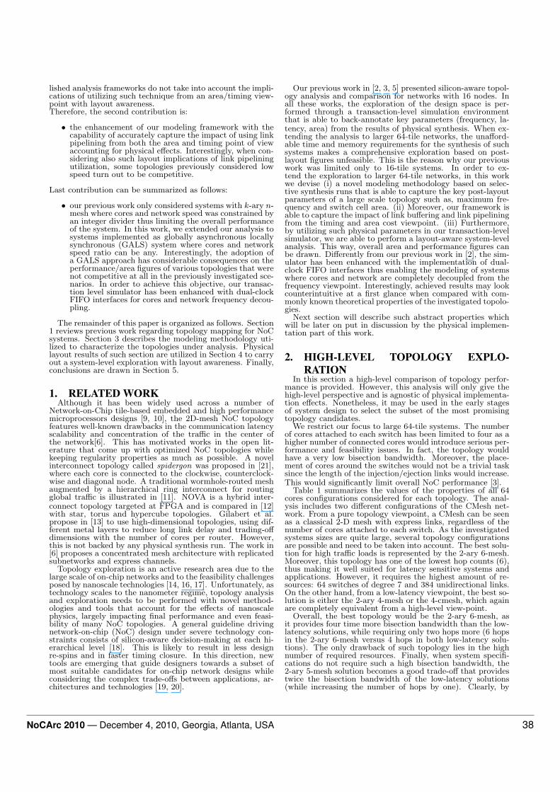
From the area viewpoint (see Figure 2), it is interesting tonote that this result is influenced by the combination of manyparameters such as: number of switches in the topology, theirradix and consequently their final working frequency. In fact,as explained above, in order to be accurate, all representativeswitches in every topology have been re-synthesized at thefinal working speed of the whole network.
0
0.2
0.4
0.6
0.8
1
1.2
8-ary 2-mesh
8-cmesh
4-ary 3-mesh
2-ary 6-mesh
2-ary 5-mesh
4-ary 2-mesh
2-ary 4-mesh
4-cmesh
No
rma
lize
d A
rea
Area
Figure 2: Normalized area for 64-tile topologies.
As an example, let us consider a very slow topology like 2-ary 6-mesh that features a larger area footprint with respect tothe 8-ary 2-mesh. Such a network is operating at a frequencymuch slower than the 8-ary 2-mesh, but since it has an equalnumber of switches (64) with a higher radix (8 vs. 4, 5 or 6),the overall area figures plays in favor of the 8-ary 2-mesh witha 10% saving.
Another interesting result concerns the 4-ary 2-mesh. Thistopology has a relatively short link (3mm), thus it does
not suffer from a large speed degradation after place-and-route. As reported in Table 2, this topology is the only one(along with 8-ary 2-mesh) to have a final working speed above500MHz. Interestingly, the area footprint of such topology hasa 20% saving with respect to the 8-ary 2-mesh as it only has16 switches. Although their radix is 10, 11 and 12, their finalworking speed along with the number of their instances resultsto be more area effective than the 8-ary 2-mesh counterpart.
The overall conclusion is that most of the topologies arenot competitive with the 8-ary 2-mesh because of their longlinks that influence the final working speed. A natural wayto tackle this problem is to implement link pipelining on suchlong links but the policy of insertion has to be carefully engi-neered. In fact, the studied 64-tile topologies feature a highnumber of long links that could rapidly bring the area cost toan unaffordable budget for a system-on-chip.
3.3 Pipeline stage insertion for 64-tile systemsIn order to cope with the high speed degradation of most
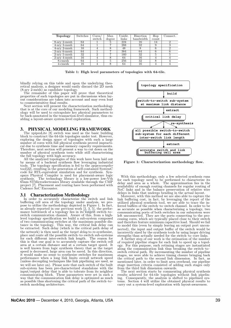
topologies analyzed in the previous section, pipeline stagesneed to be inserted especially in the top dimensions. Byadding pipeline stages, it is possible to partially (if not com-pletely) recover the initial operating frequency of the basicswitch block. The criteria that has been adopted for the in-sertion of pipeline stages is to use them only from the thirdlink dimension onwards. Therefore, topologies such has 8-ary2-mesh and 4-ary 2-mesh have not been modified. Table 3collects the results of this experiment. As clearly reported inthe 3rd and 4th column, the insertion of pipeline stages is avery effective way to reduce post-place and route frequencydegradation. Column 5 reports the number of pipeline stagesinferred in each link dimension whereas the 6th column pointsout the number of links of each topology. The area weightcomes from the combination of these two factors and it is re-ported in the 7th column. Total cell area of the topologiesalong with the contribution of such retiming stages insertionis reported in Figure 3.
0
0.5
1
1.5
2
2.5
8-ary 2-mesh
8-cmesh
4-ary 3-mesh
2-ary 6-mesh
2-ary 5-mesh
4-ary 2-mesh
2-ary 4-mesh
4-cmesh
Norm
aliz
ed A
rea
switchpipeline stage
Figure 3: Normalized area for 64-tile topologies withpipeline stages.
Please note that the number of pipeline stages per link de-pends on the maximum achievable frequency (dictated by themaximum switch radix) along with the link length which is anintrinsic characteristic of each topology. As reported in Fig-ure 3, the 2-ary 6-mesh is the most area greedy topology be-cause it has the highest number of switches (64) and they wereplaced and routed at the high frequency of 855MHz. More-over, this topology features 192 links with up to 5 pipelinestages on the longest interconnection channel. The key takeaway is that, for each topology, there is a different price topay to restore the possible working frequency allowed by theelementary switch block. For this reason, Section 4 will in-troduce the throughput/area metric (or area efficiency) thatprovides a fair assessment of the cost of the achievable band-width in each topology (see Figure 6(b)).
To conclude the physical implementation part, it is inter-
NoCArc 2010 — December 4, 2010, Georgia, Atlanta, USA 40
topology radix post-synthesis post-P&R # of pipe-stage num. links tot. pipe-stage area to.t switch impact of pipe-stagefrequency frequency per dimension area (um2) area (um2) insertion on tot. switch area
8-ary 2-mesh 6 1.08GHz 893MHz 0 112 0 2327712.8 0%8-cmesh 6 1.08GHz 893MHz express link⇒4 128 193425.9 2752108.8 7.03%
4-ary 3-mesh 8 950MHz 855MHz dim.3⇒4 144 660216.3 3182953.2 20.74%2-ary 6-mesh 8 950MHz 855MHz dim.3,4⇒1, dim.5,6⇒5 192 1087918.1 4362092.8 24.94%2-ary 5-mesh 9 810MHz 562MHz dim.3⇒1, dim.4.5⇒3 80 293081.6 2758480.4 10.62%4-ary 2-mesh 12 720MHz 532MHz 0 24 0 1860718.3 0%2-ary 4-mesh 12 720MHz 532MHz dim.3,4⇒3 32 125574.7 2328426.4 5.39%
4-cmesh 12 720MHz 532MHz express link⇒3 32 62787.4 2328426.4 2.69%
Table 3: Post-place&route results of 64-tile topologies with pipeline stage insertion.
1e+06
1.5e+06
2e+06
2.5e+06
3e+06
3.5e+06
4e+06
4.5e+06
5e+06
5.5e+06
8-ary 2-mesh
8-cmesh
4-ary 3-mesh
2-ary 6-mesh
2-ary 5-mesh
4-ary 2-mesh
2-ary 4-mesh
4-cmesh
Are
a (
um
2)
baselinewith pipelining
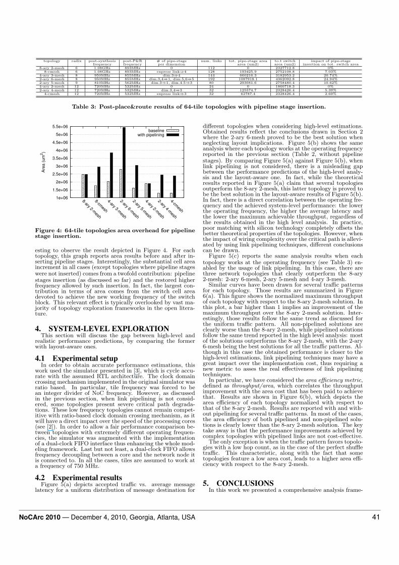
Figure 4: 64-tile topologies area overhead for pipelinestage insertion.
esting to observe the result depicted in Figure 4. For eachtopology, this graph reports area results before and after in-serting pipeline stages. Interestingly, the substantial cell areaincrement in all cases (except topologies where pipeline stageswere not inserted) comes from a twofold contribution: pipelinestages insertion (as discussed so far) and the restored higherfrequency allowed by such insertion. In fact, the largest con-tribution in terms of area comes from the switch cell areadevoted to achieve the new working frequency of the switchblock. This relevant effect is typically overlooked by vast ma-jority of topology exploration frameworks in the open litera-ture.
4. SYSTEM-LEVEL EXPLORATIONThis section will discuss the gap between high-level and
realistic performance predictions, by comparing the formerwith layout-aware ones.
4.1 Experimental setupIn order to obtain accurate performance estimations, this
work used the simulator presented in [3], which is cycle accu-rate with the assumed RTL architecture. The clock domaincrossing mechanism implemented in the original simulator wasratio based. In particular, tile frequency was forced to bean integer divider of NoC frequency. However, as discussedin the previous section, when link pipelining is not consid-ered, some topologies present severe critical path degrada-tions. These low frequency topologies cannot remain compet-itive with ratio-based clock domain crossing mechanism, as itwill have a direct impact over the speed of the processing cores(see [2]). In order to allow a fair performance comparison be-tween topologies with extremely different operating frequen-cies, the simulator was augmented with the implementationof a dual-clock FIFO interface thus enhancing the whole mod-eling framework. Last but not least, a dual-clock FIFO allowsfrequency decoupling between a core and the network node itis connected to. In all the cases, tiles are assumed to work ata frequency of 750 MHz.
4.2 Experimental resultsFigure 5(a) depicts accepted traffic vs. average message
latency for a uniform distribution of message destination for
different topologies when considering high-level estimations.Obtained results reflect the conclusions drawn in Section 2where the 2-ary 6-mesh proved to be the best solution whenneglecting layout implications. Figure 5(b) shows the sameanalysis where each topology works at the operating frequencyreported in the previous section (Table 2, without pipelinestages). By comparing Figure 5(a) against Figure 5(b), whenlink pipelining is not considered, there is a misleading gapbetween the performance predictions of the high-level analy-sis and the layout-aware one. In fact, while the theoreticalresults reported in Figure 5(a) claim that several topologiesoutperform the 8-ary 2-mesh, this latter topology is proved tobe the best solution in the layout-aware results of Figure 5(b).In fact, there is a direct correlation between the operating fre-quency and the achieved system-level performance: the lowerthe operating frequency, the higher the average latency andthe lower the maximum achievable throughput, regardless ofthe results obtained in the high level analysis. In practice,poor matching with silicon technology completely offsets thebetter theoretical properties of the topologies. However, whenthe impact of wiring complexity over the critical path is allevi-ated by using link pipelining techniques, different conclusionscan be drawn.
Figure 5(c) reports the same analysis results when eachtopology works at the operating frequency (see Table 3) en-abled by the usage of link pipelining. In this case, there arethree network topologies that clearly outperform the 8-ary2-mesh: 2-ary 6-mesh, 2-ary 5-mesh and 4-ary 3-mesh.
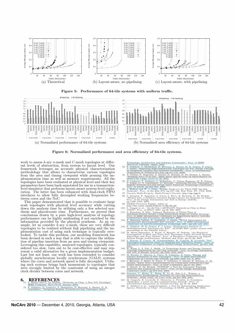
Similar curves have been drawn for several traffic patternsfor each topology. Those results are summarized in Figure6(a). This figure shows the normalized maximum throughputof each topology with respect to the 8-ary 2-mesh solution. Inthis plot, a bar higher than 1 implies an improvement of themaximum throughput over the 8-ary 2-mesh solution. Inter-estingly, those results follow the same trend as discussed forthe uniform traffic pattern. All non-pipelined solutions areclearly worse than the 8-ary 2-mesh, while pipelined solutionsfollow the same trend reported in the high level analysis: mostof the solutions outperforms the 8-ary 2-mesh, with the 2-ary6-mesh being the best solutions for all the traffic patterns. Al-though in this case the obtained performance is closer to thehigh-level estimations, link pipelining techniques may have agreat impact over the implementation cost, thus requiring anew metric to asses the real effectiveness of link pipeliningtechniques.
In particular, we have considered the area efficiency metric,defined as throughput/area, which correlates the throughputimprovement with the area cost that has been paid to achievethat. Results are shown in Figure 6(b), which depicts thearea efficiency of each topology normalized with respect tothat of the 8-ary 2-mesh. Results are reported with and with-out pipelining for several traffic patterns. In most of the cases,the area efficiency of both pipelined and non-pipelined solu-tions is clearly lower than the 8-ary 2-mesh solution. The keytake away is that the performance improvements achieved bycomplex topologies with pipelined links are not cost-effective.
The only exception is when the traffic pattern favors topolo-gies with a low hop count, as in the case of the perfect shuffletraffic. This characteristic, along with the fact that sometopologies feature a low area cost, leads to a higher area effi-ciency with respect to the 8-ary 2-mesh.
5. CONCLUSIONSIn this work we presented a comprehensive analysis frame-
NoCArc 2010 — December 4, 2010, Georgia, Atlanta, USA 41
0
0.1
0.2
0.3
0.4
0.5
20 40 60 80 100 120 140
Aver
age
Mes
sage
Lat
ency
(ns)
Traffic (flits/ns/node)
8-ary 2-mesh4-ary 3-mesh2-ary 6-mesh2-ary 5-mesh2-ary 4-mesh4-ary 2-mesh
8-cmesh4-cmesh
(a) Theoretical
0
0.1
0.2
0.3
0.4
0.5
20 40 60 80 100 120 140
Aver
age
Mes
sage
Lat
ency
(ns)
Traffic (flits/ns/node)
8-ary 2-mesh4-ary 3-mesh2-ary 6-mesh2-ary 5-mesh2-ary 4-mesh4-ary 2-mesh
8-cmesh4-cmesh
(b) Layout-aware, no pipelining
0
0.1
0.2
0.3
0.4
0.5
20 40 60 80 100 120 140
Aver
age
Mes
sage
Lat
ency
(ns)
Traffic (flits/ns/node)
8-ary 2-mesh4-ary 3-mesh2-ary 6-mesh2-ary 5-mesh2-ary 4-mesh4-ary 2-mesh
8-cmesh4-cmesh
(c) Layout-aware, with pipelining
Figure 5: Performance of 64-tile systems with uniform traffic.
0
0,2
0,4
0,6
0,8
1
1,2
1,4
1,6
1,8
2
Bit
reve
rsal
Bu
tter
fly
Ho
tsp
ot
Per
fect
Sh
uff
le
Un
ifo
rm
Bit
reve
rsal
Bu
tter
fly
Ho
tsp
ot
Per
fect
Sh
uff
le
Un
ifo
rm
Bit
reve
rsal
Bu
tter
fly
Ho
tsp
ot
Per
fect
Sh
uff
le
Un
ifo
rm
Bit
reve
rsal
Bu
tter
fly
Ho
tsp
ot
Per
fect
Sh
uff
le
Un
ifo
rm
Bit
reve
rsal
Bu
tter
fly
Ho
tsp
ot
Per
fect
Sh
uff
le
Un
ifo
rm
Bit
reve
rsal
Bu
tter
fly
Ho
tsp
ot
Per
fect
Sh
uff
le
Un
ifo
rm
Bit
reve
rsal
Bu
tter
fly
Ho
tsp
ot
Per
fect
Sh
uff
le
Un
ifo
rm
4-ary 3-mesh 2-ary 6-mesh 2-ary 5-mesh 2-ary 4-mesh 4-ary 2-mesh 8-cmesh 4-cmesh
Pipelining No Pipelining
(a) Normalized performance of 64-tile systems
0
0,2
0,4
0,6
0,8
1
1,2
1,4
Bit
reve
rsal
Bu
tter
fly
Ho
tsp
ot
Perf
ect
Shu
ffle
Un
ifo
rm
Bit
reve
rsal
Bu
tter
fly
Ho
tsp
ot
Perf
ect
Shu
ffle
Un
ifo
rm
Bit
reve
rsal
Bu
tter
fly
Ho
tsp
ot
Perf
ect
Shu
ffle
Un
ifo
rm
Bit
reve
rsal
Bu
tter
fly
Ho
tsp
ot
Perf
ect
Shu
ffle
Un
ifo
rm
Bit
reve
rsal
Bu
tter
fly
Ho
tsp
ot
Perf
ect
Shu
ffle
Un
ifo
rm
Bit
reve
rsal
Bu
tter
fly
Ho
tsp
ot
Perf
ect
Shu
ffle
Un
ifo
rm
Bit
reve
rsal
Bu
tter
fly
Ho
tsp
ot
Perf
ect
Shu
ffle
Un
ifo
rm
4-ary 3-mesh 2-ary 6-mesh 2-ary 5-mesh 2-ary 4-mesh 4-ary 2-mesh 8-cmesh 4-cmesh
Pipelining No Pipelining
(b) Normalized area efficiency of 64-tile systems
Figure 6: Normalized performance and area efficiency of 64-tile systems.
work to assess k-ary n-mesh and C-mesh topologies at differ-ent levels of abstraction, from system to layout level. Ourframework leverages an accurate physical characterizationmethodology that allows to characterize various topologiesfrom the area and timing viewpoint while pruning the im-plementation time as well as memory requirements. All thetopologies have been evaluated at physical level and their keyparameters have been back-annotated for use in a transaction-level simulator that performs layout-aware system-level explo-ration. The latter has been enhanced with dual-clock FIFOinterfaces to allow fully decoupled working frequencies be-tween cores and the NoC.
This paper demonstrated that is possible to evaluate largescale topologies with physical level accuracy while cuttingdown the analysis time by utilizing only a few selected syn-thesis and place&route runs. Furthermore, we proved thatconclusions drawn by a pure high-level analysis of topologyperformance can be highly misleading if not enriched by theinformation provided by the physical synthesis. As an ex-ample, let us consider k-ary n-mesh, these are very difficulttopologies to be realized without link pipelining and the im-plementation cost of using such technique is typically over-looked. To tackle this problem, our modeling framework hasbeen devised in such a way that is able to capture the utiliza-tion of pipeline insertion from an area and timing viewpoint.Leveraging this capability, analyzed topologies, typically con-sidered too slow, turn out to be cost-effective and may rep-resent a valid alternative for a given implementation budget.Last but not least, our work has been extended to considerglobally asynchronous locally synchronous (GALS) systemswhere the cores and network speed is fully decoupled. Utiliz-ing such systems brings back momentum to topologies thatwere strongly limited by the constraint of using an integerclock divider between cores and network.
6. REFERENCES[1] L. Benini and G. De Micheli, “Networks on Chip: a New SoC Paradigm”.
IEEE Computer, 35(1):70-78, January 2002.[2] F. Gilabert, D. Ludovici, S. Medardoni, D. Bertozzi, L. Benini, G. N.
Gaydadjiev, “Designing Regular Network-on-Chip Topologies under
Technology, Architecture and Software Constraints”. Proc. of IEEEMuCoCos, Fukuoka, Japan, 2009.
[3] F. Gilabert, S. Medardoni, D. Bertozzi, L. Benini, M. E. Gomez, P. Lopez,J. Duato, “Exploring High-Dimensional Topologies for NoC Design Throughan Integrated Analysis and Synthesis Framework”. Proc. of InternationalSymposium on Network-on-Chip, pp.107-116, 2008.
[4] A. Pullini, F. Angiolini, S. Murali, D. Atienza, G. De Micheli, L. Benini,“Bringing NoCs to 65 nm”. IEEE Micro Special Issue on Interconnects forMulti-Core Chips, 27(5):75–78, 2007.
[5] D. Ludovici, F. Gilabert, S. Medardoni, C. Gomez Requena, M. E. Gomez,P. Lopez, G. N. Gaydadjiev, D. Bertozzi, “Assessing Fat-tree Topologies forRegular Network-on-Chip Design under Nanoscale Technology Constraints”.Proc. of DATE, pp.562–565, 2009.
[6] J. Balfour and W. J. Dally, “Design Trade-o↑s for Tiled CMP On-chipNetworks”. Proc. of the 20th ICS, pp.187–198, New York, NY, USA, 2006.
[7] Circuits Multi-Projects, Multi-Project Circuits; http://cmp.imag.fr
[8] S. Stergiou, F. Angiolini, S. Carta, L. Ra↑o, D. Bertozzi, G. De Micheli,“XPipes Lite: a Synthesis Oriented Design Library for Networks on Chips”.Proc. of the Design Automation and Test in Europe (DATE),pp.1188–1193, 2005.
[9] TILE64 Processor Family, online athttp://www.tilera.com/pdf/ProBrief_Tile64_Web.pdf
[10] S. Vangal et al., “An 80-Tile 1.28TFLOPS Network-on-Chip in 65nmCMOS”. Proc. of ISSCC 2007, pp.98–589, 2007.
[11] S. Bourduas, Z. Zilic, “Latency Reduction of Global Tra¡c inWormhole-Routed Meshes Using Hierarchical Rings for Global Routing”.Proc. of IEEE International Conference on Application-Speci↓c Systems,Architectures and Processors, pp.302-307, 2007.
[12] F. Martinez Vallina, N. Jachimiec, J. Saniie, “NOVA Interconnect forDynamically Recon↓gurable NoC systems”. Proc. of IEEE InternationalConference on Electro/Information Technology, 2007, pp.546–550, 2007.
[13] F. Gilabert, M. E. Gomez, P. J. Lopez, “Performance Analysis ofMultidimensional Topologies for NoC”. ACACES 2007, poster session withproceedings at the Summer School.
[14] M. Mirza-Aghatabar, S. Koohi, S. Hessabi, M. Pedram, “An EmpiricalInvestigation of Mesh and Torus NoC Topologies Under Di↑erent RoutingAlgorithms and Tra¡c Models”. Proc. of Euromicro Conference on DigitalSystem Design Architectures, Methods and Tools, pp.19–26, 2007.
[15] L. Bononi, N. Concer, M. Grammatikakis, M. Coppola, R. Locatelli, “NoCTopologies Exploration based on Mapping and Simulation Models”. Proc. ofEuromicro Conference on Digital System Design Architectures, pp.543–546,2007.
[16] H. Wang, L. S. Peh, S. Malik, “A Technology-Aware and Energy OrientedTopology Exploration for On-Chip Networks”. Proc. of Design Automationand Test in Europe (DATE), pp.1238–1243, 2005.
[17] M. Kreutz, C. Marcon, L. Carro, N. Calazans, A. Susin, “Energy andLatency Evaluation of NoC Topologies”. Proc. of IEEE InternationalSymposium on Circuits and Systems, pp.5866–5869 Vol. 6, 2005.
[18] I. Hatirnaz, S. Badel, N. Pazos, Y. Leblebici, S. Murali, D. Atienza, G. DeMicheli, “Early Wire Characterization for Predictable Network-on-ChipGlobal Interconnects”. Proc. of SLIP Conference, pp.57–64, 2007.
[19] S. Murali, G. De Micheli, “SUNMAP: a Tool for Automatic TopologySelection and Generation for NoCs”. Proc. of the Design AutomationConference (DAC), pp.914–914, 2004.
[20] Soteriou, V., Eisley, N., Wang, H., Li, B., Peh, L.S., “Polaris: aSystem-Level Roadmapping Toolchain for On-Chip InterconnectionNetworks”. IEEE Trans. on VLSI 15(8), pp.855–868, 2007.
[21] M. Coppola, R. Locatelli, G. Maruccia, L. Pieralisi, A. Scandurra,“Spidergon: a novel on-chip communication network”. Proc. ofInternational Symposium on System-on-Chip, pp.16–18, 2004.
[22] A. Jalabert et al., “xpipesCompiler: a Tool for Instantiating ApplicationSpeci↓c Networks on Chip”. Proceedings of DATE, pp.884–889, 2004.
NoCArc 2010 — December 4, 2010, Georgia, Atlanta, USA 42