
Formal Verification of Arithmetic Masking in Hardware and ...
Upload
khangminh22Category
view
0download
0
A Hardware Verification
Methodology for an Interconnection
Network with fast Process
Synchronization
Inauguraldissertation
zur Erlangung des akademischen Grades
eines Doktors der Naturwissenschaften
der Universitat Mannheim
vorgelegt von
Niels Martin Burkhardt
(Diplom-Informatiker der Technischen Informatik)
aus Mannheim
Mannheim, 2012

Dekan Professor Dr. H. J. Muller, Universitat Mannheim
Referent Professor Dr. U. Bruning, Universitat Heidelberg
Korreferent Professor Dr. H. Froning, Universitat Heidelberg
Tag der mundlichen Prufung: 19.03.2013


Abstract
Shrinking process node sizes allow the integration of more and more functionality into
a single chip design. At the same time, the mask costs to manufacture a new chip
increases steadily. For the industry this cost increase can be absorbed by selling more chips.
Furthermore, new innovative chip designs have a higher risk. Therefore, the industry only
changes small parts of a chip design between different generations to minimize their risks.
Thus, new innovative chip designs can only be realized by research institutes, which do not
have the cost restrictions and the pressure from the markets as the industry.
Such an innovative research project is EXTOLL, which is developed by the Computer
Architecture Group of the University of Heidelberg. It is a new interconnection network
for High Performance Computing, and targets the problems of existing interconnection
networks commercially available. EXTOLL is optimized for a high bandwidth, a low
latency, and a high message rate. Especially, the low latency and high message rate become
more important for modern interconnection networks. As the size of networks grow, the
same computational problem is distributed to more nodes. This leads to a lower data
granularity and more smaller messages, that have to be transported by the interconnection
network.
The problem of smaller messages in the interconnection network is addressed by this
thesis. It develops a new network protocol, which is optimized for small messages. It reduces
the protocol overhead required for sending small messages. Furthermore, the growing
network sizes introduce a reliability problem. This is also addressed by the developed
efficient network protocol.
The smaller data granularity also increases the need for an efficient barrier synchronization.
Such a hardware barrier synchronization is developed by thesis, using a new approach of
integrating the barrier functionality into the interconnection network.
The masks costs to manufacture an ASIC make it difficult for a research institute to
build an ASIC. A research institute cannot afford re-spin, because of the costs. Therefore,
there is the pressure to make it right the first time. An approach to avoid a re-spin is
the functional verification in prior to the submission. A complete and comprehensive
verification methodology is developed for the EXTOLL interconnection network. Due to
the structured approach, it is possible to realize the functional verification with limited
v
resources in a small time frame. Additionally, the developed verification methodology is
able to support different target technologies for the design with a very little overhead.
vi

Zusammenfassung
Die Verkleinerung der Prozessgroßen ermoglicht es immer mehr Funktionalitat in einen Chip
zu integrieren. Gleichzeitig steigen die Kosten fur die Produktion eines Chips stetig. Die
Industrie kann diese Kostensteigerung auffangen, in dem sie mehr Chips verkauft. Zusatzlich
haben neue innovative Chipdesigns ein hoheres Risiko. Um ihr Risiko zu minimieren, andert
die Industrie nur kleine Teile eines Chips zwischen aufeinander folgenden Generationen. Das
fuhrt dazu, dass neue innovative Chipdesigns nur noch von Forschungsinstituten entwickelt
werde, die nicht dem gleichen Kostendruck unterliegen.
Ein solches innovatives Forschungsprojekt ist EXTOLL von dem Lehrstuhl fur Rech-
nerarchitektur der Universitat Heidelberg. Es ist ein neues Verbindungsnetzwerk fur das
Hochleistungsrechnen, und zielt darauf ab die existierenden Probleme von kommerziell
verfugbaren Verbindungsnetzwerken zu losen. Es ist optimiert fur eine hohe Bandbreite,
eine kleine Latenz und eine hohe Nachrichtenrate. Insbesondere, die kleine Latenz und die
hohe Nachrichtenrate werden immer wichtiger fur moderne Verbindungsnetzwerke. In dem
Maße in dem die Große der Verbindungsnetzwerke steigt, werden Berechnungsprobleme auf
immer mehr Rechner verteilt. Das fuhrt dazu, dass die Datengranularitat immer kleiner
wird und damit die Nachrichten, die in einem Verbindungsnetzwerk transportiert werden
mussen.
Das Problem der verkleinerten Datengranularitat in Verbindungsnetzwerken wird von
der vorliegenden Arbeit behandelt. Sie entwickelt ein neues Netzwerkprotokoll, das fur
kleine Nachrichtengroßen optimiert ist. Es verringert den Aufwand, der benotigt wird
um kleine Nachrichten zu versenden. Zusatzlich verursachen steigende Netzwerkgroßen
ein Zuverlassigkeitsproblem, welches bei dem entwickelten effizienten Netzwerkprotokoll
berucksichtigt wird.
Die kleinere Datengranularitat vergroßert die Notwendigkeit nach einer effizienten Barrier-
ensynchronisation. Eine solche Barrierensynchronisation wird in der vorliegenden Arbeit
entwickelt. Dabei wird ein neuer Ansatz verwendet, um die Barrierensynchronisation in ein
Verbindungsnetzwerk zu integrieren.
Die steigenden Maskenkosten um einen ASIC zu produzieren, machen es fur ein Forsch-
ungsinstitut schwer, einen ASIC zu entwickeln. Ein Forschungsinstitut kann es sich aufgrund
der Kosten nicht leisten einen ASIC zweimal zu fertigen. Aufgrund dessen muss der ASIC
vii

nach der ersten Fertigung funktionieren. Eine Moglichkeit, eine zweite Fertigung zu ver-
meiden ist die Verwendung der funktionalen Verifikation bevor der Chip gefertigt wird.
Dafur wurde eine komplette und vollstandige Verifikation Methodik fur das EXTOLL
Verbindungsnetzwerk entwickelt. Durch die strukturierte Herangehensweise ist es moglich
die funktionale Verifikation mit begrenzten Ressourcen in einem kleinen Zeitfenster zu
realisieren. Zusatzlich ermoglicht es die entwickelte Verifikationsmethodik mehrere Zieltech-
nologien mit einem kleinen Zusatzaufwand zu unterstutzen.
viii
Contents
1. Introduction 1
1.1. Outline . . . . . . . . . . . . . . . . . . . . . . . . . . . . . . . . . . . . . . 3
2. Network Protocols 5
2.1. Introduction . . . . . . . . . . . . . . . . . . . . . . . . . . . . . . . . . . . . 5
2.2. Protocol Requirements . . . . . . . . . . . . . . . . . . . . . . . . . . . . . . 6
2.3. State of the Art Networks . . . . . . . . . . . . . . . . . . . . . . . . . . . . 7
2.3.1. Ethernet . . . . . . . . . . . . . . . . . . . . . . . . . . . . . . . . . . 8
2.3.2. Infiniband . . . . . . . . . . . . . . . . . . . . . . . . . . . . . . . . . 8
2.3.3. Cray Gemini . . . . . . . . . . . . . . . . . . . . . . . . . . . . . . . 11
2.3.4. IBM Blue Gene . . . . . . . . . . . . . . . . . . . . . . . . . . . . . . 12
2.3.5. TOFU Network . . . . . . . . . . . . . . . . . . . . . . . . . . . . . . 13
2.3.6. TianHe-1A . . . . . . . . . . . . . . . . . . . . . . . . . . . . . . . . 14
2.4. Fault Tolerant Network Protocols . . . . . . . . . . . . . . . . . . . . . . . . 14
2.4.1. EXTOLLr1 Protocol . . . . . . . . . . . . . . . . . . . . . . . . . . . 16
2.4.2. EXTOLLr2 Network Protocol . . . . . . . . . . . . . . . . . . . . . . 18
2.4.2.1. Protocol Layers . . . . . . . . . . . . . . . . . . . . . . . . 19
2.4.2.2. Cell Definition . . . . . . . . . . . . . . . . . . . . . . . . . 22
2.4.2.3. Network Layer . . . . . . . . . . . . . . . . . . . . . . . . . 25
2.4.2.4. Link Layer . . . . . . . . . . . . . . . . . . . . . . . . . . . 27
2.4.2.5. Protocol Analysis . . . . . . . . . . . . . . . . . . . . . . . 32
3. Barrier Synchronization 33
3.1. Barrier Requirements . . . . . . . . . . . . . . . . . . . . . . . . . . . . . . . 34
3.2. Barrier Design Space Evaluation . . . . . . . . . . . . . . . . . . . . . . . . 35
3.2.1. Software Barrier . . . . . . . . . . . . . . . . . . . . . . . . . . . . . 35
3.2.1.1. Counter based Barrier . . . . . . . . . . . . . . . . . . . . . 36
3.2.1.2. Butterfly Barrier . . . . . . . . . . . . . . . . . . . . . . . . 36
3.2.2. Hardware Barrier . . . . . . . . . . . . . . . . . . . . . . . . . . . . . 37
3.2.2.1. Dedicated Barrier Network . . . . . . . . . . . . . . . . . . 37
3.2.2.2. Integrated Barrier Network . . . . . . . . . . . . . . . . . . 39
3.3. State of the Art . . . . . . . . . . . . . . . . . . . . . . . . . . . . . . . . . . 40
ix
Contents
3.4. EXTOLL Barrier . . . . . . . . . . . . . . . . . . . . . . . . . . . . . . . . . 40
3.4.1. Performance Evaluation . . . . . . . . . . . . . . . . . . . . . . . . . 43
4. Functional Verification 45
4.1. Verification Methodology . . . . . . . . . . . . . . . . . . . . . . . . . . . . 49
4.1.1. Verification Techniques . . . . . . . . . . . . . . . . . . . . . . . . . 49
4.1.1.1. Transaction Based Verification . . . . . . . . . . . . . . . . 50
4.1.1.2. Random Constraint Verification . . . . . . . . . . . . . . . 51
4.1.1.3. Coverage Driven Verification . . . . . . . . . . . . . . . . . 52
4.1.1.4. Assertion Based Verification . . . . . . . . . . . . . . . . . 53
4.1.2. Simulation Based Verification . . . . . . . . . . . . . . . . . . . . . . 54
4.1.3. Formal Verification . . . . . . . . . . . . . . . . . . . . . . . . . . . . 55
4.1.4. Verification Hierarchy . . . . . . . . . . . . . . . . . . . . . . . . . . 58
4.1.5. Verification Planning . . . . . . . . . . . . . . . . . . . . . . . . . . . 60
4.1.6. Verification Cycle . . . . . . . . . . . . . . . . . . . . . . . . . . . . . 62
4.1.7. Universal Verification Methodology . . . . . . . . . . . . . . . . . . . 64
4.1.7.1. Universal Verification Components . . . . . . . . . . . . . . 65
4.1.7.2. UVM Phases . . . . . . . . . . . . . . . . . . . . . . . . . . 68
4.1.7.3. UVM Configuration Mechanism . . . . . . . . . . . . . . . 71
4.1.7.4. UVM Factory . . . . . . . . . . . . . . . . . . . . . . . . . 71
4.1.7.5. UVM based Test Bench . . . . . . . . . . . . . . . . . . . . 72
4.1.7.6. Connecting UVCs . . . . . . . . . . . . . . . . . . . . . . . 72
4.2. EXTOLL Functional Verification . . . . . . . . . . . . . . . . . . . . . . . . 74
4.2.1. Functional Verification Roles . . . . . . . . . . . . . . . . . . . . . . 74
4.2.2. EXTOLL Verification Analysis . . . . . . . . . . . . . . . . . . . . . 75
4.2.3. Verification Infrastructure . . . . . . . . . . . . . . . . . . . . . . . . 87
4.2.3.1. Subversion Directory Structure . . . . . . . . . . . . . . . . 87
4.2.3.2. Testbench Run Script . . . . . . . . . . . . . . . . . . . . . 93
4.2.4. Unit Verification . . . . . . . . . . . . . . . . . . . . . . . . . . . . . 94
4.2.4.1. RMA . . . . . . . . . . . . . . . . . . . . . . . . . . . . . . 94
4.2.4.2. Barrier . . . . . . . . . . . . . . . . . . . . . . . . . . . . . 113
4.2.5. Chip Level Verification . . . . . . . . . . . . . . . . . . . . . . . . . . 113
4.2.5.1. Checking Strategy . . . . . . . . . . . . . . . . . . . . . . . 114
4.2.5.2. Stimulus Generation . . . . . . . . . . . . . . . . . . . . . . 117
4.2.6. Regression Analysis . . . . . . . . . . . . . . . . . . . . . . . . . . . 133
4.2.7. FPGA Acceleration . . . . . . . . . . . . . . . . . . . . . . . . . . . 136
4.2.8. Conclusion . . . . . . . . . . . . . . . . . . . . . . . . . . . . . . . . 138
4.3. Verification Tools . . . . . . . . . . . . . . . . . . . . . . . . . . . . . . . . . 138
4.3.1. Testbench Creator . . . . . . . . . . . . . . . . . . . . . . . . . . . . 139
x
Contents
5. Conclusion 141
A. SystemVerilog Assertions 145
A.1. Introduction . . . . . . . . . . . . . . . . . . . . . . . . . . . . . . . . . . . . 145
A.2. Assertion Types . . . . . . . . . . . . . . . . . . . . . . . . . . . . . . . . . . 145
A.2.1. Immediate Assertions . . . . . . . . . . . . . . . . . . . . . . . . . . 146
A.2.2. Concurrent Assertions . . . . . . . . . . . . . . . . . . . . . . . . . . 147
A.3. Properties . . . . . . . . . . . . . . . . . . . . . . . . . . . . . . . . . . . . . 147
A.4. Sequences . . . . . . . . . . . . . . . . . . . . . . . . . . . . . . . . . . . . . 149
A.4.1. Sequence Operators . . . . . . . . . . . . . . . . . . . . . . . . . . . 149
A.5. Local Variables . . . . . . . . . . . . . . . . . . . . . . . . . . . . . . . . . . 150
A.6. Assertion Writing Guidelines . . . . . . . . . . . . . . . . . . . . . . . . . . 151
A.7. System Functions . . . . . . . . . . . . . . . . . . . . . . . . . . . . . . . . . 152
A.8. SVA Examples . . . . . . . . . . . . . . . . . . . . . . . . . . . . . . . . . . 152
xi

List of Figures
2.1. Ethernet Frame . . . . . . . . . . . . . . . . . . . . . . . . . . . . . . . . . . 9
2.2. IP Header . . . . . . . . . . . . . . . . . . . . . . . . . . . . . . . . . . . . . 9
2.3. TCP Header . . . . . . . . . . . . . . . . . . . . . . . . . . . . . . . . . . . 9
2.4. Infiniband Packet . . . . . . . . . . . . . . . . . . . . . . . . . . . . . . . . . 11
2.5. Gemini Packet . . . . . . . . . . . . . . . . . . . . . . . . . . . . . . . . . . 12
2.6. Error Handling . . . . . . . . . . . . . . . . . . . . . . . . . . . . . . . . . . 15
2.7. EXTOLLr1 Packet . . . . . . . . . . . . . . . . . . . . . . . . . . . . . . . . 17
2.8. EXTOLLr2 Protocol Layers . . . . . . . . . . . . . . . . . . . . . . . . . . . 20
2.9. General Control Cell Format . . . . . . . . . . . . . . . . . . . . . . . . . . 23
2.10. Initialization Cell Format . . . . . . . . . . . . . . . . . . . . . . . . . . . . 23
2.11. Node ID Cell Format . . . . . . . . . . . . . . . . . . . . . . . . . . . . . . . 23
2.12. Credit Cell Format . . . . . . . . . . . . . . . . . . . . . . . . . . . . . . . . 24
2.13. Acknowledgment Cell Format . . . . . . . . . . . . . . . . . . . . . . . . . . 24
2.14. Start of Packet Cell Format . . . . . . . . . . . . . . . . . . . . . . . . . . . 25
2.15. End of Packet Cell Format . . . . . . . . . . . . . . . . . . . . . . . . . . . . 25
2.16. Barrier Cell Format . . . . . . . . . . . . . . . . . . . . . . . . . . . . . . . 25
2.17. EXTOLLr2 Packet . . . . . . . . . . . . . . . . . . . . . . . . . . . . . . . . 26
2.18. EXTOLLr2 Packet Alignment . . . . . . . . . . . . . . . . . . . . . . . . . . 27
2.19. Link Layer Initialization . . . . . . . . . . . . . . . . . . . . . . . . . . . . . 29
2.20. Acknowledgment Protocol . . . . . . . . . . . . . . . . . . . . . . . . . . . . 30
2.21. Retransmission Example . . . . . . . . . . . . . . . . . . . . . . . . . . . . 31
3.1. Barrier Synchronization . . . . . . . . . . . . . . . . . . . . . . . . . . . . . 34
3.2. Barrier Design Space . . . . . . . . . . . . . . . . . . . . . . . . . . . . . . . 36
3.3. Butterfly Barrier[40] . . . . . . . . . . . . . . . . . . . . . . . . . . . . . . . 37
3.4. Barrier Or Network . . . . . . . . . . . . . . . . . . . . . . . . . . . . . . . . 38
3.5. Barrier And Network . . . . . . . . . . . . . . . . . . . . . . . . . . . . . . . 39
3.6. Barrier Overview . . . . . . . . . . . . . . . . . . . . . . . . . . . . . . . . . 40
4.1. Verification Reconvergence Model . . . . . . . . . . . . . . . . . . . . . . . . 46
4.2. Verification Reconvergence Model Interpretation . . . . . . . . . . . . . . . 47
4.3. Generic Testbench . . . . . . . . . . . . . . . . . . . . . . . . . . . . . . . . 48
xiii

List of Figures
4.4. Verification Techniques . . . . . . . . . . . . . . . . . . . . . . . . . . . . . . 50
4.5. Transaction Based Verification . . . . . . . . . . . . . . . . . . . . . . . . . 51
4.6. Coverage Types . . . . . . . . . . . . . . . . . . . . . . . . . . . . . . . . . . 52
4.7. Simulation Based Verification . . . . . . . . . . . . . . . . . . . . . . . . . . 56
4.8. Formal Verification Types . . . . . . . . . . . . . . . . . . . . . . . . . . . . 56
4.9. Proof Radius . . . . . . . . . . . . . . . . . . . . . . . . . . . . . . . . . . . 58
4.10. Verification Hierarchy . . . . . . . . . . . . . . . . . . . . . . . . . . . . . . 59
4.11. Verification Plan Sections . . . . . . . . . . . . . . . . . . . . . . . . . . . . 61
4.12. Verification Cycle . . . . . . . . . . . . . . . . . . . . . . . . . . . . . . . . . 63
4.13. Verification Progress . . . . . . . . . . . . . . . . . . . . . . . . . . . . . . . 64
4.14. Interface UVC . . . . . . . . . . . . . . . . . . . . . . . . . . . . . . . . . . 65
4.15. Module UVC . . . . . . . . . . . . . . . . . . . . . . . . . . . . . . . . . . . 68
4.16. UVM Phases . . . . . . . . . . . . . . . . . . . . . . . . . . . . . . . . . . . 69
4.17. UVM Objections . . . . . . . . . . . . . . . . . . . . . . . . . . . . . . . . . 70
4.18. UVM Testbench . . . . . . . . . . . . . . . . . . . . . . . . . . . . . . . . . 72
4.19. UVM Layering . . . . . . . . . . . . . . . . . . . . . . . . . . . . . . . . . . 74
4.20. EXTOLL Overview . . . . . . . . . . . . . . . . . . . . . . . . . . . . . . . . 76
4.21. EXTOLL Interface UVC Library . . . . . . . . . . . . . . . . . . . . . . . . 77
4.22. HT Core Interfaces . . . . . . . . . . . . . . . . . . . . . . . . . . . . . . . . 77
4.23. BQ Interfaces . . . . . . . . . . . . . . . . . . . . . . . . . . . . . . . . . . . 78
4.24. WCB Interfaces . . . . . . . . . . . . . . . . . . . . . . . . . . . . . . . . . . 79
4.25. VELO Interfaces . . . . . . . . . . . . . . . . . . . . . . . . . . . . . . . . . 80
4.26. RMA Interfaces . . . . . . . . . . . . . . . . . . . . . . . . . . . . . . . . . . 81
4.27. SMFU Interfaces . . . . . . . . . . . . . . . . . . . . . . . . . . . . . . . . . 82
4.28. ATU Interfaces . . . . . . . . . . . . . . . . . . . . . . . . . . . . . . . . . . 83
4.29. NP Interfaces . . . . . . . . . . . . . . . . . . . . . . . . . . . . . . . . . . . 83
4.30. Crossbar Interfaces . . . . . . . . . . . . . . . . . . . . . . . . . . . . . . . . 85
4.31. LP Interfaces . . . . . . . . . . . . . . . . . . . . . . . . . . . . . . . . . . . 86
4.32. Barrier Interfaces . . . . . . . . . . . . . . . . . . . . . . . . . . . . . . . . . 86
4.33. Subversion Directory Structure . . . . . . . . . . . . . . . . . . . . . . . . . 89
4.34. TB Directory Structure . . . . . . . . . . . . . . . . . . . . . . . . . . . . . 90
4.35. CAG Testbench Hierarchy . . . . . . . . . . . . . . . . . . . . . . . . . . . . 92
4.36. RMA UVC . . . . . . . . . . . . . . . . . . . . . . . . . . . . . . . . . . . . 95
4.37. RMA TB Overview . . . . . . . . . . . . . . . . . . . . . . . . . . . . . . . . 102
4.38. RMA User Sequences . . . . . . . . . . . . . . . . . . . . . . . . . . . . . . . 105
4.39. Chip Verification Decision . . . . . . . . . . . . . . . . . . . . . . . . . . . . 114
4.40. EXTOLL interfaces . . . . . . . . . . . . . . . . . . . . . . . . . . . . . . . . 114
4.41. Chip Verification Overview . . . . . . . . . . . . . . . . . . . . . . . . . . . 116
4.42. EXTOLL traffic directions . . . . . . . . . . . . . . . . . . . . . . . . . . . . 117
xiv
List of Figures
4.43. Link Environment . . . . . . . . . . . . . . . . . . . . . . . . . . . . . . . . 118
4.44. North Bridge UVC . . . . . . . . . . . . . . . . . . . . . . . . . . . . . . . . 120
4.45. VELO Environment . . . . . . . . . . . . . . . . . . . . . . . . . . . . . . . 123
4.46. RMA Environment . . . . . . . . . . . . . . . . . . . . . . . . . . . . . . . . 126
4.47. SMFU Environment . . . . . . . . . . . . . . . . . . . . . . . . . . . . . . . 127
4.48. Virtual Sequencer References . . . . . . . . . . . . . . . . . . . . . . . . . . 130
4.49. Regression HTML Report . . . . . . . . . . . . . . . . . . . . . . . . . . . . 134
4.50. Regression eManager Report . . . . . . . . . . . . . . . . . . . . . . . . . . 135
4.51. Ventoux Board . . . . . . . . . . . . . . . . . . . . . . . . . . . . . . . . . . 136
xv

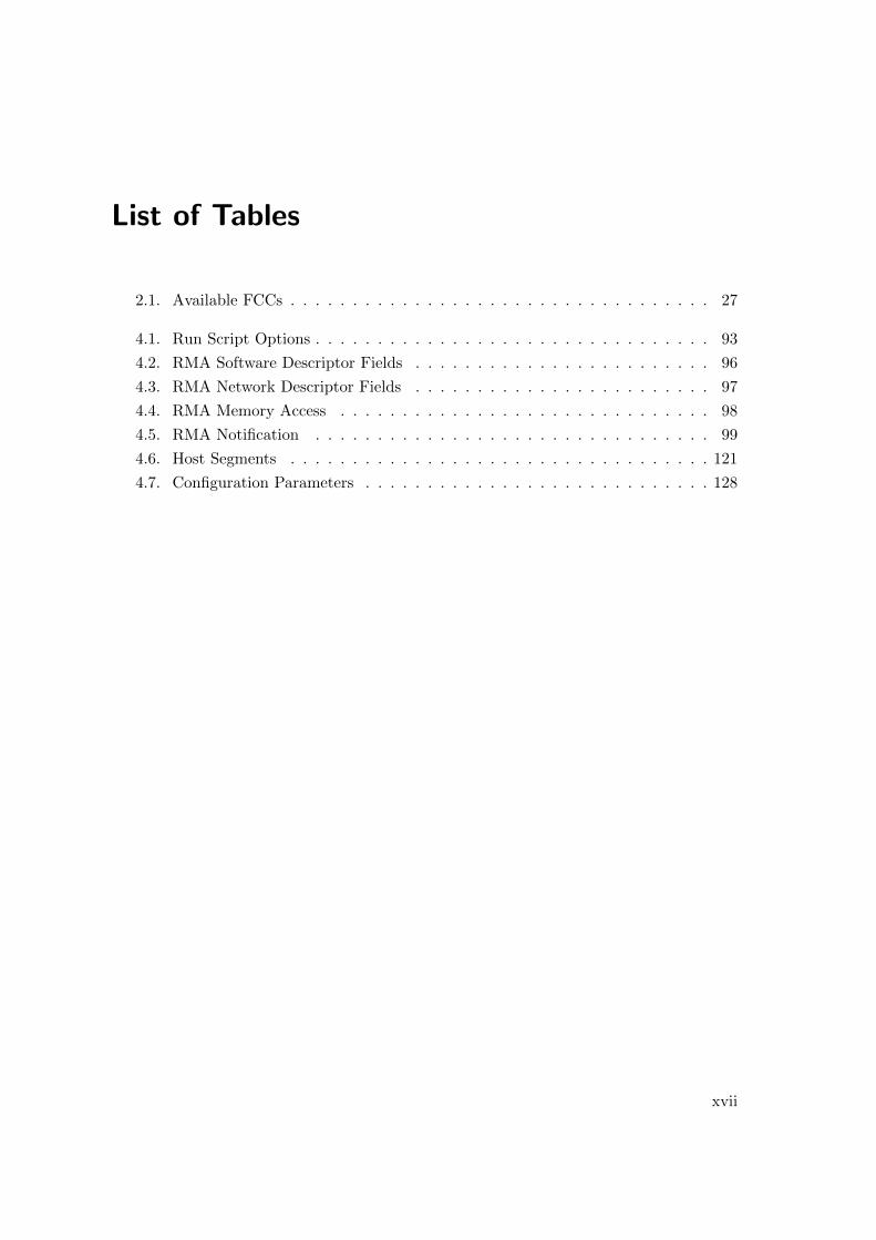
List of Tables
2.1. Available FCCs . . . . . . . . . . . . . . . . . . . . . . . . . . . . . . . . . . 27
4.1. Run Script Options . . . . . . . . . . . . . . . . . . . . . . . . . . . . . . . . 93
4.2. RMA Software Descriptor Fields . . . . . . . . . . . . . . . . . . . . . . . . 96
4.3. RMA Network Descriptor Fields . . . . . . . . . . . . . . . . . . . . . . . . 97
4.4. RMA Memory Access . . . . . . . . . . . . . . . . . . . . . . . . . . . . . . 98
4.5. RMA Notification . . . . . . . . . . . . . . . . . . . . . . . . . . . . . . . . 99
4.6. Host Segments . . . . . . . . . . . . . . . . . . . . . . . . . . . . . . . . . . 121
4.7. Configuration Parameters . . . . . . . . . . . . . . . . . . . . . . . . . . . . 128
xvii


Acronyms
ACK Acknowledgment.
ASIC Application Specific Integrated Circuit.
ATOLL Atomic Low Latency.
ATU Address Translation Unit.
BAR Base Address Register.
BDD Binary Decision Diagram.
BER Bit Error Rate.
BFM Bus Functional Model.
BIOS Basic Input Output System.
BQ Buffer Queue.
BTH Base Transport Header.
CAG Computer Architecture Group.
CDV Coverage Driven Verification.
CPU Central Processing Unit.
CRC Cyclic Redundancy Check.
DETH Datagram Extended Transport Header.
DMA Direct Memory Access.
DUV Design under Verification.
EDA Electronic Design Automation.
EOF End of Flit.
EOP End of Packet.
EOP E End of Packet with Error.
EXTOLL Extended ATOLL.
xix

Acronyms
FCC Flow Control Channel.
FDR Fourteen Data Rate.
FIFO First In First Out.
Flit flow control digits.
FPGA Field Programmable Gate Array.
FSM Finite State Machine.
FU Functional Unit.
FV Functional Verification.
GAT Global Address Table.
GDS Graphic Database System.
GPU Graphics Processing Unit.
GUID Globally Unique Identifier.
HPC High Performance Computing.
HT HyperTransport.
HTAX HyperTransport Advanced Crossbar.
HTML Hyper Text Markup Language.
HTOC HyperTransport on Chip Protocol.
HW Hardware.
I2C Inter-Integrated Circuit.
I/O Input Output.
IBTA InfiniBand Trade Association.
ID Identifier.
IP Internet Protocol.
IP Intellectual Property.
LP Link Port.
LRH Local Routing Header.
MB MegaByte.
MDV Metric Driven Verification.
MPI Message Passing Interface.
MTU Maximum Transfer Unit.
xx

Acronyms
NACK Not Acknowledgment.
NIC Network Interface Controller.
NLA Network Logical Address.
NP Network Port.
OS Operation System.
PCIe Peripheral Component Interconnect Express.
PDID Protection Domain Identifier.
PGAS Partitioned Global Address Space.
PHIT Physical Unit.
PIO Programmed Input/Output.
PLL Phase Looked Loop.
PSL Property Specification Language.
RAM Random Access Memory.
RCV Random Constraint Verification.
RDETH Reliable Datagram Extended Transport Header.
RDMA Remote Direct Memory Access.
RETH RDMA Extended Transport Header.
RF Register File.
RFS Register File Surrogate.
RGM Register Modeling.
RMA Remote Memory Access Unit.
RTL Register Transfer Level.
RX Receive.
SAT Conjunctive Normal Form Satisfiability.
SCB Scoreboard.
SMFU Shared Memory Functional Unit.
SNQ System Notification Queue.
SOC System on a Chip.
SOF Start of Flit.
SOP Start of Packet.
xxi
Acronyms
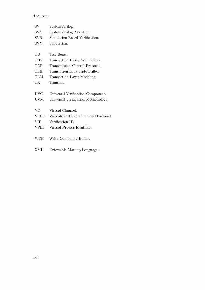
SV SystemVerilog.
SVA SystemVerilog Assertion.
SVB Simulation Based Verification.
SVN Subversion.
TB Test Bench.
TBV Transaction Based Verification.
TCP Transmission Control Protocol.
TLB Translation Look-aside Buffer.
TLM Transaction Layer Modeling.
TX Transmit.
UVC Universal Verification Component.
UVM Universal Verification Methodology.
VC Virtual Channel.
VELO Virtualized Engine for Low Overhead.
VIP Verification IP.
VPID Virtual Process Identifier.
WCB Write Combining Buffer.
XML Extensible Markup Language.
xxii

1. Introduction
Nowadays, the development of new complex hardware designs is driven by the industry.
Shrinking process node sizes enables hardware engineers to integrate more functional logic
into a single chip from generation to generation. As more functionality is integrated, also
the verification of the implemented designs is getting more complex. In the design teams
more members are assigned for the verification than for the hardware implementation.
Meanwhile, the time available to build a new chip decreases, as there is a competition
between companies to release a new chip design first. Only then, it is possible to monetize
the investments made to build a chip. As a result, the industry has started to build new
chips by reusing building blocks, and combining them with only a small amount of new
functionality into Systems on a Chip (SOCs). These building blocks are either used from
previous designs or are bought from third party vendors. This development can be best
seen for mobile devices. There are many different SOCs available for these devices. But,
the used Central Processing Units (CPUs), Graphics Processing Units (GPUs), and other
blocks, are developed by only a couple of companies. Therefore, the differences between
chip generations decrease, as new innovative approaches and designs are too cost intensive.
In contrast, research institutes do not have the same time and cost restrictions as the
industry on the one hand. On the other hand, they have limited resources regarding to
funding and manpower. Furthermore, they do not have the pressure from the markets to
release new chips regularly. Therefore, they can think about and implement new innovative
chip designs. In this process they are not forced to rely on building blocks. Instead, they
are able to build everything from scratch, which enables them to optimize every aspect of
a design. This includes the system architecture as well as the transistor level.
Building new innovative hardware designs consists of two design phases. First, there
is an architectural phase, in which the features, the concepts, and the architecture of a
design are explored and defined. This phase is dominated by simulations to analyze and
understand the system behavior. But, a simulation uses predetermined synthetic workloads
only, as it is difficult to model and map real workloads to a simulation. Thus, in a second
phase a hardware implementation of the design is done to validate, that the system meets
the expectations regrading to scalability and performance.
This implementation is done in the form of an Application Specific Integrated Circuit
1
1. Introduction
(ASIC). Building an ASIC is a demanding task for a research institute. Due to its limited
resources, the implementation process must be very efficient. In addition, there is the
pressure to make it the first time right. Due to increasing mask costs, a re-spin is not
affordable by a research institute. Therefore, a sophisticated functional verification method-
ology is needed to get the confidence, that the chip behaves like intended. Furthermore,
the functional verification must be done with limited manpower.
Such an innovative research project is Extended ATOLL (EXTOLL) of the Computer
Architecture Group (CAG) of the University of Heidelberg. The performance gain of
supercomputers and computers used for cloud computing and big data applications is
mainly driven by an increasing grade of parallelism. The single thread performance does not
scale with the needs for more computing power any more. Consequently, these computers
are build using thousands of compute nodes, which are connected by an interconnection
network. Whereas the performance of the compute nodes increases steadily, the performance
of the available interconnection networks does not scale in the same way. The goal of
EXTOLL is to build a new interconnection network for High Performance Computing
(HPC) to address the existing drawbacks of the commercial interconnection networks
available. EXTOLL is optimized for a high bandwidth, a low latency, and a high message
rate. It is a complete own design to have the flexibility to optimize each aspect of the
interconnection network. In particular the latency and the message rate are getting an
issue with growing network sizes. As the network size grows, also the grade of parallelism
grows, which results in a lower granularity of the processed data. Therefore, more small
messages must be transported by the network. The lower granularity leads to a decreasing
computation time proportional to the transportation time of the data in the network.
This development must be taken care of in the design phase of a modern interconnection
network. Because, more small messages are used also the network protocol has to be
optimized therefore. To allow a high bandwidth and message rate even for small messages,
the framing of the network protocol has to be as small as possible. Additionally, the fault
tolerance of a network is getting an issue with growing network sizes. As more nodes
are involved, also the amount of physical connections between the nodes increases, which
results in a higher probability of bit errors in the whole network. Therefore, reliability
mechanisms are needed for the network protocol to detect and correct errors in the network
with a low overhead. These problems are addressed by this thesis, which develops a new
efficient network protocol with low overhead for small messages and a strong fault tolerance.
The lower data granularity raises another problem. Many parallel codes solve a compu-
tational problem iteratively. Thereby, the computational task is scattered among several
compute nodes, where each node processes a part of the whole problem. To proceed with
the computation, the nodes have to exchange their intermediate results in regular intervals.
At these exchange points, all nodes have to wait until all other ones have reached this
2
1.1. Outline
point, too. This synchronization is done by a collective operation called a barrier. The
time duration of a barrier synchronization must be as short as possible, as during the
synchronization all compute nodes are not able to proceed with the computation. Due to
a smaller data granularity, more synchronization points are needed, which raises the need
for a very efficient and short barrier synchronization. Therefore, this thesis proposes a new
way to integrate a barrier synchronization into an unified interconnection network.
As mentioned above, an ASIC implementation of a new hardware design is needed
to show and validate its system behavior and performance. Due to the manufacturing
costs of an ASIC, a research institute can not afford a re-spin in the case of an erroneous
implementation. Consequently, it must be ensured in prior to the submission of the ASIC,
that the implementation is functionally correct. Because of the limited resources of a
research institute, the functional verification has to be very productive and needs to be
applied in a reasonable time frame. Furthermore, in a research context Field Programmable
Gate Arrays (FPGAs) are used as a prototyping platform. As they are reprogrammable,
new hardware designs can be tested quickly, but with a limited performance. Additionally,
finding bugs in an FPGA is a time consuming task, although they are reprogrammable.
For the functional verification of such a project, there are different requirements. First,
different target technologies must be supported. On the one hand, there are FPGA
implementations, and on the other hand, there is the ASIC. Second, it has to be done with
limited resources, and of course, it must be complete, in order that all bugs are found,
before the tape out. To be able to handle the complexity of the functional verification
process, an efficient and complete methodology must be used. Such a methodology is
developed by this thesis.
1.1. Outline
This thesis is divided into four chapters. The first chapter introduces a new network
protocol for a HPC interconnection network. It describes the requirements for such a
network, and shows how an efficient network protocol improves the performance of an
interconnection network. Furthermore, reliability aspects of interconnection networks and
their impact on the network protocol are discussed.
The second chapter gives an example of fast barrier synchronization in an unified
interconnection network. In addition, an implementation of a global interrupt logic is
shown.
The third chapter concentrates on the functional verification methodology for a large
hardware design. It demonstrates, how the verification of a new hardware design can be
organized to reach verification closure in a short time frame with limited resources, and
3
1. Introduction
explains the structure of the whole verification environment. All parts of the environment
are described in depth. Thereby, it is revealed, how reusable verification components and a
hierarchical verification approach improves the verification process, and shortens the time
needed for a successful functional verification.
The last chapter summarizes thesis with a reflection about the achievements made and
the impact on this work.
4
2. Network Protocols
2.1. Introduction
The number of compute nodes used in supercomputers increases steadily [1]. This growth
will become more and more critical in the transition from petascale to exascale computing.
The interconnection network, which is used for the communication between the nodes,
becomes a critical component with the increasing node count. While computational
intensive benchmarks like High Performance Linpack [2] show a performance improvement
[3] over time, network intensive benchmarks as G-RandomAccess and G-FFTE [3] do
not improve in the same way. In contrast to compute nodes, which are built using
commodity hardware, commodity interconnection networks as Ethernet [4] do not deliver
the performance needed for HPC. These commodity networks are designed to fit for different
heterogeneous environments. Thus, each network layer is defined to be easily exchangeable
by a different technology, which causes a high overhead in the network protocol stack.
Furthermore, they implement many features, that are not needed for HPC. For example, a
typical interconnection network for HPC needn’t to be globally addressable. Therefore,
homogeneous interconnections networks, which are used for HPC, should be optimized
for this use case to improve its performance. To address these problems with commodity
networks, several interconnection networks were developed for HPC like [5], [6], [7], or
EXTOLL.
To measure the performance of an interconnection network three key metrics are used:
the bandwidth, the latency, and the message rate. The bandwidth measures the amount of
data, that can be delivered by a network in a second. As the size of networks grows and the
compute nodes are able to process more data in the same time frame, also the bandwidth
of the interconnection network needs to grow accordingly. The latency measures the time
from a message is generated at its source node until it gets delivered at its destination
node. During the time a message needs to traverse the network, its data can’t be processed
as well as the the compute nodes can be blocked as they wait for a message to be received
or until the message is delivered. Therefore, a low latency improves the performance of a
network. The message rate counts the number of messages that can be delivered by an
interconnection network in a time frame. Particularly for parallel codes, which use many
small messages for synchronization, a high message rate improves the overall performance.
5
2. Network Protocols
The growing network sizes lead to smaller messages, which an interconnection network
has to transport. This is caused by distributing a computational problem to more nodes.
Thereby, each node processes a smaller data set. For this reason, also smaller messages
are exchanged by the nodes. Thus, the interconnection network needs to be optimized for
small messages, in order to sent small messages with a low latency at a high message rate.
As the sizes of interconnection networks grow, also their fault tolerance is getting an
issue. The kinds of faults, that an interconnection network has to deal with, mainly include
bit errors on physical links, and complete failures of links or compute nodes. With the
growing size also the amount of physical links for connecting the compute nodes increases,
which increases the overall probability of faults in the whole system. A network fault that
is not detected causes programs executed on the system either to fail or to progress with
wrong data, when the fault occurred within the data of a network packet. Therefore, an
interconnection network needs to ensure a reliable operation, which includes the ability to
recover from faults.
2.2. Protocol Requirements
A key factor for the overall performance and fault tolerance of an interconnection network
is its network protocol. It defines how data is transferred in the network. This includes
how the data is assembled into packets, the packet types that are available, the framing of
a packet, the routing and fault tolerance mechanisms.
The requirements for an interconnection network are defined in [8]. From this, the
following key requirements for a network protocol can be derived.
Scalability Scalability means for a network, that when additional nodes are added to the
network, also the performance of the network has to increase accordingly to avoid
that the network becomes a bottleneck. For the network protocol it follows, that
it must be able to address these additional nodes. Moreover, the network protocol
should not restrict the number of nodes in the network, which reduces its scalability.
The reliability mechanisms for an interconnection network depend on retransmission
buffers to hold the transmitted data until it is completely received by the destination.
When additional nodes are added, the total buffer space needs to be increased, too.
For a scalable network, the buffer space should not limit the size of the network.
Efficiency Data, that is transferred in the network, normally can not be injected directly
into the network. The data is assembled into packets to be able to share the network
between different transfers. Therefore, the data is framed to mark the start and the
end of the data. This framing includes the destination node for the packet and all
6
2.3. State of the Art Networks
other information needed by the network to forward a packet to its destination node.
As the framing reduces the bandwidth, which is available to send data, it has to be
as compact as possible for an efficient network. The efficiency of a network protocol
can be calculated with the following formula:
Efficiency =Payload Size
Packet Size(2.1)
Whereas the payload size is the size of the data to be sent, and the packet size the
size of the data including the packet framing.
Reliability The reliability of a network describes its ability to recover from network faults.
As faults are getting an issue with growing network sizes, the reliability mechanisms
of the network protocol must be able to recover from any faults that have occurred.
The reliability of a network can be increased either by error detection or by error
correction. With an error detection, the network detects errors in the transmitted
data. To able to recover from an error, the data sent must be stored in an extra buffer
before the transmission. When an error is detect, the corrupted data is retransmitted
from that buffer. These buffers can be located in the sending node of a message.
The receiving node checks the message, and requests retransmission of the message
from the sender in the case of an error. This is called an end to end retransmission.
Another method is the link retransmission, in which the messages are checked at
a per link basis. Thus, the buffers are located in each link of the network and the
retransmission is done in the link layer in the case of an error. From a scalability
point of view, the link retransmission scales better than the end to end retransmission,
as by a link retransmission each new node adds it own buffers. In contrast to the
end to end retransmission, which needs larger buffers with each added node.
An error correction detects and corrects faults on the fly. Therefore, hamming codes
are normally used. To be able to fix detected errors they have to add additional
information to the data transferred, which in return reduces the efficiency of the
network protocol.
2.3. State of the Art Networks
There are several interconnection networks available, which are used to connect the compute
nodes of supercomputers. The following sections will describe the most important ones.
7
2. Network Protocols
2.3.1. Ethernet
Ethernet [4] is the most widely used commodity network. It was firstly introduced in 1980,
and today the specified data rates range from 10 megabits to 100 gigabits. That’s why, it
is used in home networking as well as supercomputers.
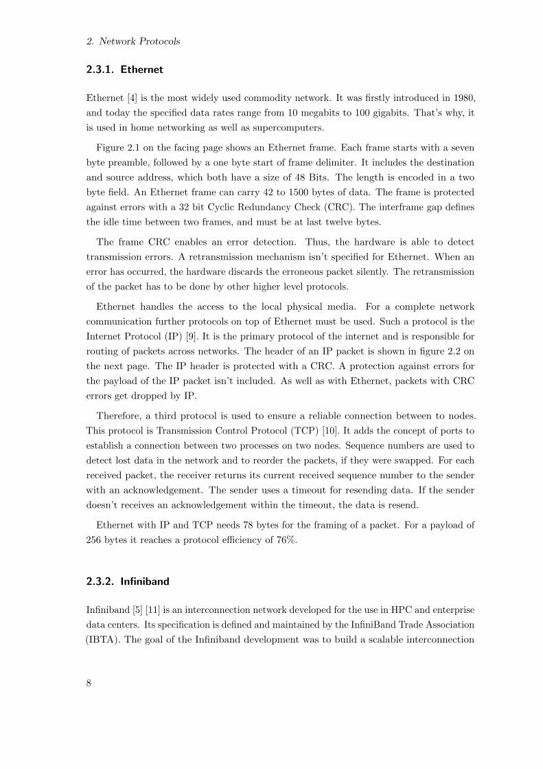
Figure 2.1 on the facing page shows an Ethernet frame. Each frame starts with a seven
byte preamble, followed by a one byte start of frame delimiter. It includes the destination
and source address, which both have a size of 48 Bits. The length is encoded in a two
byte field. An Ethernet frame can carry 42 to 1500 bytes of data. The frame is protected
against errors with a 32 bit Cyclic Redundancy Check (CRC). The interframe gap defines
the idle time between two frames, and must be at last twelve bytes.
The frame CRC enables an error detection. Thus, the hardware is able to detect
transmission errors. A retransmission mechanism isn’t specified for Ethernet. When an
error has occurred, the hardware discards the erroneous packet silently. The retransmission
of the packet has to be done by other higher level protocols.
Ethernet handles the access to the local physical media. For a complete network
communication further protocols on top of Ethernet must be used. Such a protocol is the
Internet Protocol (IP) [9]. It is the primary protocol of the internet and is responsible for
routing of packets across networks. The header of an IP packet is shown in figure 2.2 on
the next page. The IP header is protected with a CRC. A protection against errors for
the payload of the IP packet isn’t included. As well as with Ethernet, packets with CRC
errors get dropped by IP.
Therefore, a third protocol is used to ensure a reliable connection between to nodes.
This protocol is Transmission Control Protocol (TCP) [10]. It adds the concept of ports to
establish a connection between two processes on two nodes. Sequence numbers are used to
detect lost data in the network and to reorder the packets, if they were swapped. For each
received packet, the receiver returns its current received sequence number to the sender
with an acknowledgement. The sender uses a timeout for resending data. If the sender
doesn’t receives an acknowledgement within the timeout, the data is resend.
Ethernet with IP and TCP needs 78 bytes for the framing of a packet. For a payload of
256 bytes it reaches a protocol efficiency of 76%.
2.3.2. Infiniband
Infiniband [5] [11] is an interconnection network developed for the use in HPC and enterprise
data centers. Its specification is defined and maintained by the InfiniBand Trade Association
(IBTA). The goal of the Infiniband development was to build a scalable interconnection
8
2.3. State of the Art Networks
Figure 2.1.: Ethernet Frame
Figure 2.2.: IP Header
Figure 2.3.: TCP Header
9
2. Network Protocols
network with a low latency and high throughput. Currently, it is widely adopted in HPC,
as it can be seen in [1].
Infiniband has hardware support for two different communication mechanisms: Messaging
via (send/receive) and Remote Direct Memory Access (RDMA). Both mechanisms support
a direct user space communication. Protection keys are used to prevent the user to access
foreign data.
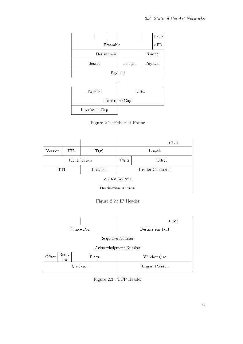
Figure 2.4 on the facing page shows an Infiniband packet for a reliable datagram
communication, which corresponds to an EXTOLL Remote Memory Access Unit (RMA)
transfer. Each packet begins with a start delimiter. It is used by the physical layer to
detect the start of packet. It is followed by the Local Routing Header (LRH). The LRH
contains the fields needed to route the packet in an Infiniband subnet. The fields include
the virtual lane, the destination and source node, and the packet length. In a subnet 216
nodes are addressable.
The Base Transport Header (BTH) contains the fields for the transport layer of Infiniband.
It includes an opcode, which specifies the transport to be used. Additionally, a packet
sequence number and the destination queue pair is included. The queue pair is the virtual
interface to the hardware for the user, and provides a virtual communication port. The
BTH is followed by the Reliable Datagram Extended Transport Header (RDETH). The
RDETH contains additional fields for the reliable datagram service. It includes a reference
to the end to end context, which is used to store the acknowledgement counters for reliability
protocol. The Datagram Extended Transport Header (DETH) includes the queue key for
access authorization of the receive queue and the source queue pair number. The RDMA
Extended Transport Header (RETH) specifies the the virtual address for the operation and
the length of the Direct Memory Access (DMA) transfer. It also includes a protection key.
Each Infiniband packet is protected against errors with two CRCs. The 32 Bits invariant
CRC covers all packet fields, that do not change from its source to its destination, and
establishes an end to end reliability. The 16 Bits variant CRC covers all fields including the
changing ones. Therefore, it is recalculated in each link before the packet is sent. When a
link receives an incoming packet, it checks its CRCs. If a CRC check fails, the packet is
discarded. The destination node returns an Acknowledgment (ACK) to the source node
on a correctly received packet. If there is an error detected by the destination node, it
returns a Not Acknowledgment (NACK). This way discarded packets in the network can
not be detected. Therefore, the requesting node starts a timeout, when it sends a packet.
If a timeout occurs for a packet, it is retransmitted. As Infiniband uses an end to end
reliability mechanism large buffers are needed on the requester side to store the packets
sent until they get acknowledged, which reduces the scalability of the network.
To improve the reliability, Infiniband Fourteen Data Rate (FDR) [11] [12] introduces a
10
2.3. State of the Art Networks
Figure 2.4.: Infiniband Packet
block error correction code for the physical layer. Each 2080 Bit block is protected by a 32
additional parity bits, and is able to correct up to 11 bit errors. As a complete block must
be received by the physical layer before it can be checked, the forward error correction
increases the latency of the network.
The framing of an Infiniband packet for a reliable datagram packet is 56 Bytes. For a
packet with 256 Bytes of payload the protocol has an efficiency of 82%.
2.3.3. Cray Gemini
Gemini [7] is a proprietary interconnection network developed by Cray. It is used in their
supercomputers. In the November 2012 Top500 list the fastest system is a Cray XK7,
which uses the Gemini network. Gemini uses a special ASIC to build a direct 3D torus
network. It is build to scale up to 100,000 nodes. The ASIC provides two Network Interface
Controllers (NICs) and a 48 port router. Gemini has communication engines for small low
latency transfers triggered by Programmed Input/Output (PIO) from the processor, large
block transfers with RDMA, and for Partitioned Global Address Space (PGAS).
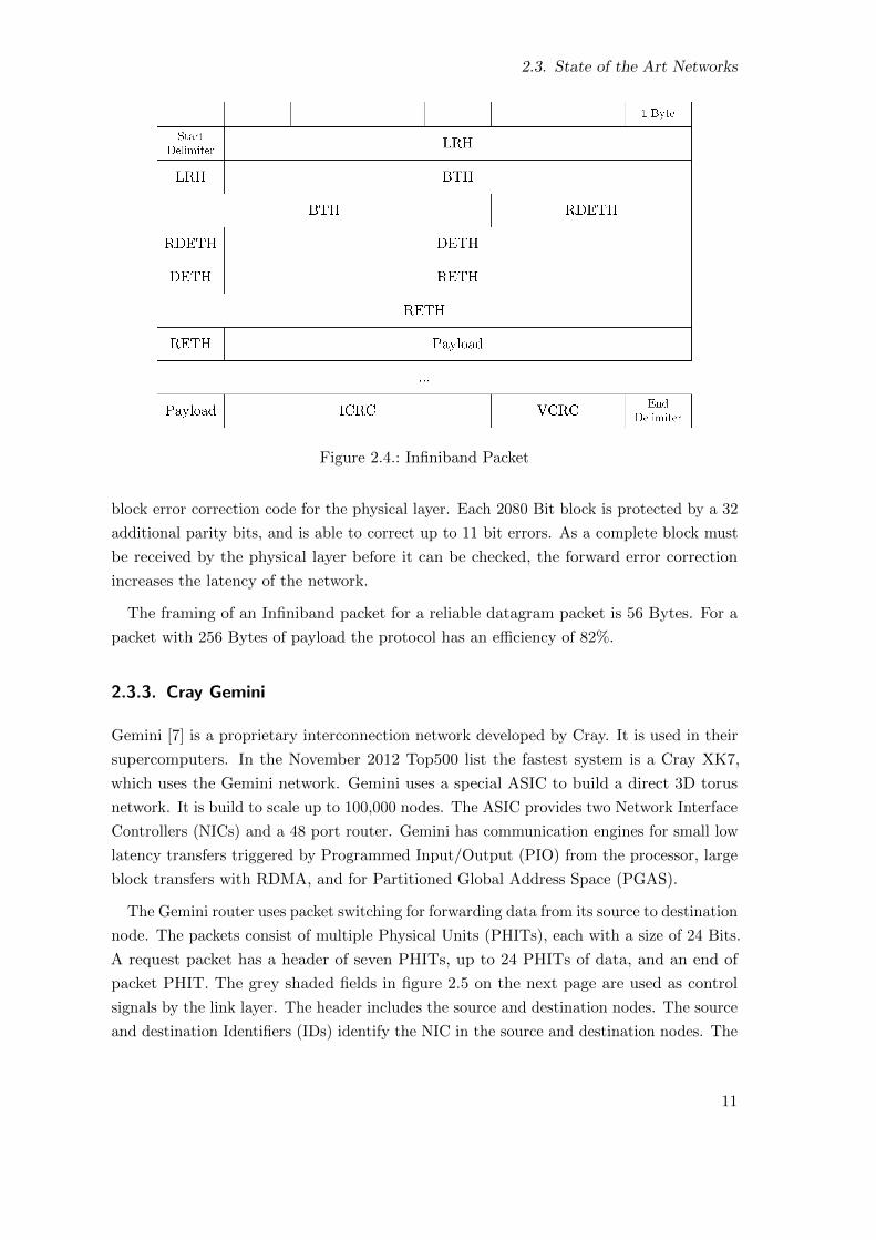
The Gemini router uses packet switching for forwarding data from its source to destination
node. The packets consist of multiple Physical Units (PHITs), each with a size of 24 Bits.
A request packet has a header of seven PHITs, up to 24 PHITs of data, and an end of
packet PHIT. The grey shaded fields in figure 2.5 on the next page are used as control
signals by the link layer. The header includes the source and destination nodes. The source
and destination Identifiers (IDs) identify the NIC in the source and destination nodes. The
11
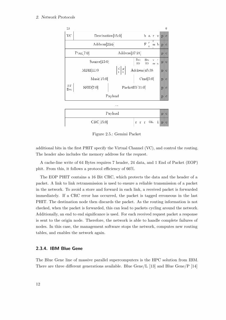
2. Network Protocols
Figure 2.5.: Gemini Packet
additional bits in the first PHIT specify the Virtual Channel (VC), and control the routing.
The header also includes the memory address for the request.
A cache-line write of 64 Bytes requires 7 header, 24 data, and 1 End of Packet (EOP)
phit. From this, it follows a protocol efficiency of 66%.
The EOP PHIT contains a 16 Bit CRC, which protects the data and the header of a
packet. A link to link retransmission is used to ensure a reliable transmission of a packet
in the network. To avoid a store and forward in each link, a received packet is forwarded
immediately. If a CRC error has occurred, the packet is tagged erroneous in the last
PHIT. The destination node then discards the packet. As the routing information is not
checked, when the packet is forwarded, this can lead to packets cycling around the network.
Additionally, an end to end significance is used. For each received request packet a response
is sent to the origin node. Therefore, the network is able to handle complete failures of
nodes. In this case, the management software stops the network, computes new routing
tables, and enables the network again.
2.3.4. IBM Blue Gene
The Blue Gene line of massive parallel supercomputers is the HPC solution from IBM.
There are three different generations available. Blue Gene/L [13] and Blue Gene/P [14]
12
2.3. State of the Art Networks
use three different proprietary interconnection networks: a tree for collective operations, a
barrier network, and a 3D Torus [6] for the main communication. The torus network has
support for send/receive and RDMA communication.
A packet has an 8 Bytes header for the link protocol. It includes a sequence number,
routing information with the destination, the virtual channel, the size of the packet, and an
8 Bit CRC for protecting the header. This CRC is checked immediately a packet is received
to ensure, that the routing information of the packet is correct. A 24 Bit CRC protects
the complete packet. A one byte valid indicator is used to tag a packet erroneous in the
case a packet CRC error has occurred. The link receiver returns an ACK to the opposite
link sender, if a packet was received without errors. The link sender uses a timeout to
resend packets, if no ACK was received. In addition a cumulative CRC is calculated for
all packets send and received by a link. This CRC can be checked by the management
software for example when a check point is written. If they don’t match an escape from
the packet CRCs has occurred, and the computation needs to be restarted from the last
check point.
For Blue Gene/Q [15] the three interconnection networks were integrated into one 5D
Torus [16] [17] network, which supports send/receive and RDMA. It also has special
hardware support for collective communication and barriers. A network packet consists
of a 32 Byte header, at which 12 Bytes are used as network header, and 20 Bytes for the
transport layer. A packet can carry up to 512 Bytes of data. 8 Bytes are for protecting
a packet against link errors. A 10 Bit Reed Solomon error correction block code is used
to protect all static fields of a packet. Additional 5 10 Bit Reed Solomon code words are
calculated and checked for each link a packet traverses. An ACK is generated in the link
for each received packet without errors. If the link sender doesn’t receive an ACK for a
packet within a given timeout, it retransmits the packet. The same additional cumulative
CRC is used as for Blue Gene/L and Blue Gene/P.
The Blue Gene/Q network protocol has an efficiency of 86% for a 256 Byte transfer.
2.3.5. TOFU Network
The K computer [18] is a supercomputer developed by RIKEN as a Japanese project.
It is a distributed memory system consisting of more than 800,000 compute nodes. An
interconnection network called TOFU [19] [20] was developed for this system to connect
the compute nodes. The network uses a 6D Torus as topology. It supports RDMA, and
has a barrier unit for synchronization and collective reduce operations.
A network packet for a put operation has a 31 Byte header. This header contains a
sequence number, the routing information, the source and destination nodes, a virtual
13
2. Network Protocols
memory address, and a global process ID. Each packet has a 17 Bytes trailer. It includes a
32 Bit end to end CRC, a 32 Bit link CRC, and an end marker. When a packet traverses
a link it is stored in a retransmission buffer. The link receiver checks the link CRC, and
returns an ACK if the CRC is correct, or a NACK otherwise. In this case the sender
retransmits the packet. An erroneous packet also gets marked in the trailer. This way, the
destination node can remove the packet. As the CRC is checked after the header with the
routing information was forwarded to the switch, erroneous packets can be cycling around
the network.
With the 48 Bit framing for a packet, TOFU reaches a network protocol efficiency of
84% for a 256 Byte put operation.
2.3.6. TianHe-1A
The TianHe-1A [21] supercomputer was built by the National University of Defense
Technology of China. It has a hybrid architecture, which uses CPUs and GPUs. The
interconnection network [22] [23] is an own development. It uses a hierarchical fat tree
topology. The network supports user level communication, has support for RDMA, two
sided communication messages with a size up to 120 Bytes, and multicast communication.
Packets are forwarded in the network using source path routing and wormhole switching.
A packet consists of four flits: one header flit and four data flits. Each flit has a size
of 256 Bits, and contains 20 Bits for sideband signaling. These bits include a 16 Bit
CRC, the virtual channel and a header/tail flag. The flits are retransmitted on a per link
basis, if the CRC computation for a received flit fails. The header flit contains a 56 Bit
NetHeader, which includes the routing string and some control information for the flow
control. As there is no information available about the header format for a RDMA transfer,
no efficiency estimation of the network protocol can be done.
2.4. Fault Tolerant Network Protocols
The amount of compute nodes used in supercomputers increases steadily. In contrast, the
Bit Error Rate (BER) of a physical connection between two nodes does not change. With
a typical BER of 10−15 for an optical link, a single bit error occurs every 27 hours. For a
3D Torus with 1000 nodes and 6000 unidirectional links, an error occurs every 16 seconds.
For a 10000 node system, an error happens every second. Therefore, the interconnection
network has to provide mechanisms to detect and correct these errors. Otherwise, the
network can not deliver any messages anymore. The error handling for packet increases its
latency, and consequently decreases the performance of the network. Thus, the reliability
14
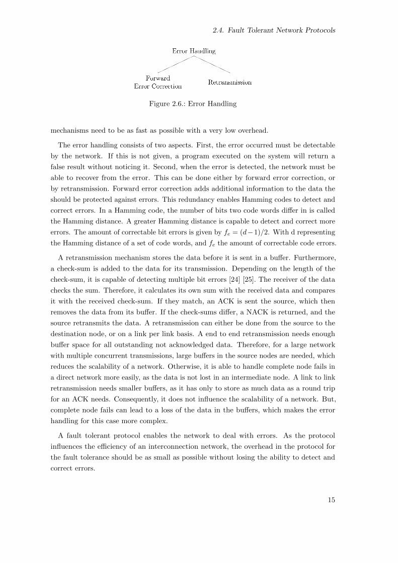
2.4. Fault Tolerant Network Protocols
Figure 2.6.: Error Handling
mechanisms need to be as fast as possible with a very low overhead.
The error handling consists of two aspects. First, the error occurred must be detectable
by the network. If this is not given, a program executed on the system will return a
false result without noticing it. Second, when the error is detected, the network must be
able to recover from the error. This can be done either by forward error correction, or
by retransmission. Forward error correction adds additional information to the data the
should be protected against errors. This redundancy enables Hamming codes to detect and
correct errors. In a Hamming code, the number of bits two code words differ in is called
the Hamming distance. A greater Hamming distance is capable to detect and correct more
errors. The amount of correctable bit errors is given by fe = (d−1)/2. With d representing
the Hamming distance of a set of code words, and fe the amount of correctable code errors.
A retransmission mechanism stores the data before it is sent in a buffer. Furthermore,
a check-sum is added to the data for its transmission. Depending on the length of the
check-sum, it is capable of detecting multiple bit errors [24] [25]. The receiver of the data
checks the sum. Therefore, it calculates its own sum with the received data and compares
it with the received check-sum. If they match, an ACK is sent the source, which then
removes the data from its buffer. If the check-sums differ, a NACK is returned, and the
source retransmits the data. A retransmission can either be done from the source to the
destination node, or on a link per link basis. A end to end retransmission needs enough
buffer space for all outstanding not acknowledged data. Therefore, for a large network
with multiple concurrent transmissions, large buffers in the source nodes are needed, which
reduces the scalability of a network. Otherwise, it is able to handle complete node fails in
a direct network more easily, as the data is not lost in an intermediate node. A link to link
retransmission needs smaller buffers, as it has only to store as much data as a round trip
for an ACK needs. Consequently, it does not influence the scalability of a network. But,
complete node fails can lead to a loss of the data in the buffers, which makes the error
handling for this case more complex.
A fault tolerant protocol enables the network to deal with errors. As the protocol
influences the efficiency of an interconnection network, the overhead in the protocol for
the fault tolerance should be as small as possible without losing the ability to detect and
correct errors.
15
2. Network Protocols
2.4.1. EXTOLLr1 Protocol
EXTOLLr1 is the successor of the Atomic Low Latency (ATOLL) interconnection network.
It is a direct network, and therefore no central switches are necessary to connect the
compute nodes. It has six bidirectional network links, which allows to built a 3D Torus
network topology. EXTOLL is optimized for a high bandwidth and a low latency for small
messages. It uses wormhole routing to forward packets from their source to destination
node. Wormhole routing transfers the network packets in a pipelined fashion. Therefore,
the packets are divided into smaller units. The flow control is done on the basis of these
units, which are called flow control digitss (Flits).
Packets are routed within the network with source path routing. Thereby, the source
node determines the route of the packet through the network. Consequently, adaptive
routing is not possible with source path routing. The advantage of source path routing is,
that the routing decision can be made very fast in every switch. This gets important for
large networks, where a packet has to cross several switches to reach its destination.
The payload of a network packet consists of three segments: the routing string, the
command, and the data. Normally, the routing string defines for each node the out port of
the switch the packet has to take. Each hop removes the part of the routing string, which
defines the current out port, when the packet is forwarded. When the packet reaches its
destination node, the routing string is completely consumed. As this results in a large string
for large networks, EXTOLL uses delta routing to compress the string. There, each part
of the routing string is valid for multiple hops. Each part has a counter for each network
dimension called x,y, and z. First, the counter for the x dimension gets decremented by one
in each hop the packet traverses until it reaches zero, followed by the y and z dimensions.
When all counters are zero, the current part is removed, and the next routing string part
is used. For distances in one dimension larger than the maximum counter value, multiple
parts must be used, were the counters of the other dimensions are set to zero.
EXTOLL uses two virtual channel groups for deadlock avoidance in the network. These
groups are divided into 4 virtual channels each to minimize the impact of head of line
blocking in a switch.
A credit based flow control is used between two node connected to each other, which
prevents buffer overflows in the switches. Each virtual channel has its own independent
credits. There are 32 credits available in total. They were chosen to guarantee a complete
link saturation[26].
The network protocol used for EXTOLLr1 was developed in [27]. It was optimized for
small messages. Thus, the protocol overhead is as small as possible. A network packet
consists of multiple PHITs. Each PHIT has a size of 16 Bit, which is equivalent to the
16
2.4. Fault Tolerant Network Protocols
Figure 2.7.: EXTOLLr1 Packet
EXTOLL’s internal data width. The size of a packet is not limited. There are control and
data PHITs available. Control PHITs are used for the framing of packets and for exchange
of control information on the link level. This includes the credits for the flow control and
the ACKs/NACKs for the retransmission protocol. Data PHITs carry the payload of the
packets.
EXTOLLr1 uses 8B/10B coding [28] as line coding. This code distinguishes between 8
Bit K-characters for the framing of packets and normal 8 Bit D-characters for data. Each
control PHIT consists of a K-character to detect the control character in the data stream.
As there are more control PHITs than K-characters, the second 8 Bit of a control PHIT
uses a D-character. The control PHITs were constructed to have a Hamming distance of 3
in the 10B space, which enables a 1 Bit error correction for control PHITs with a special
8B/10B decoder.
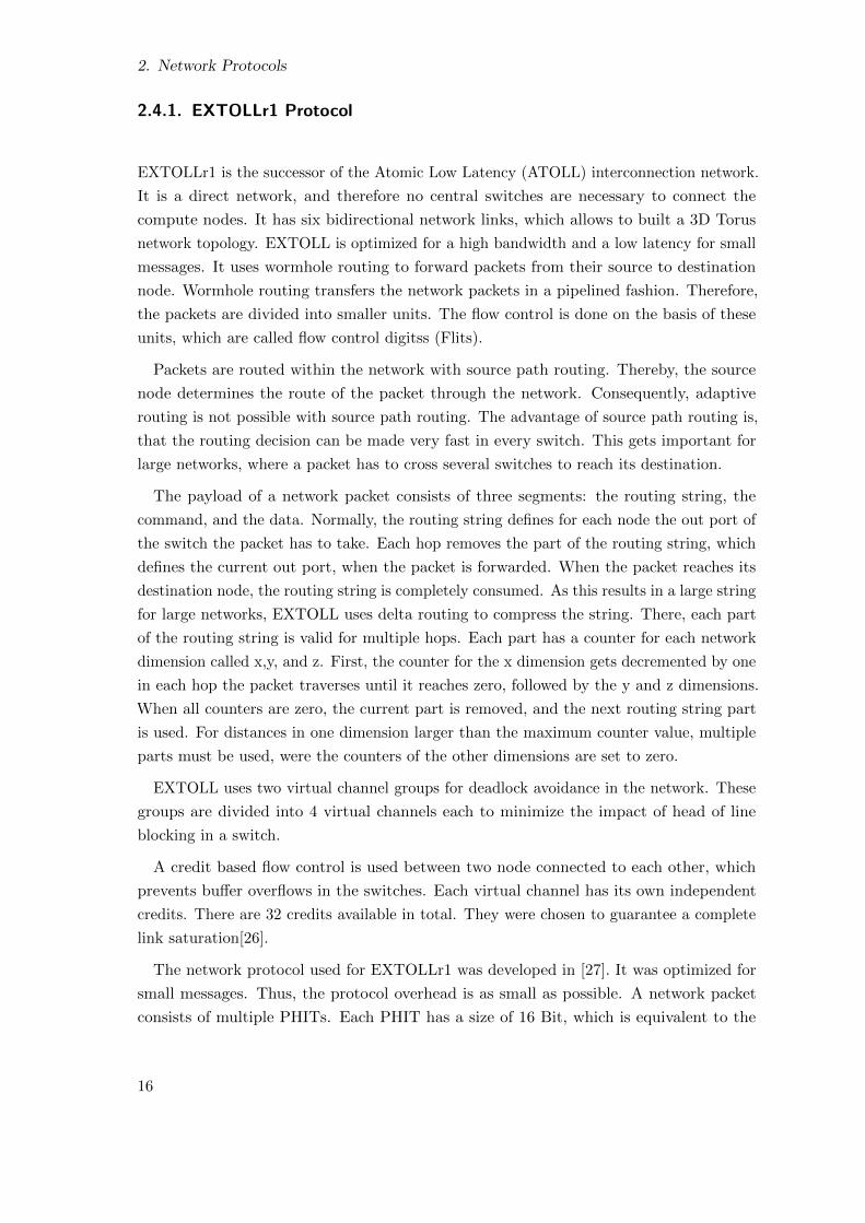
A packet(figure 2.7) starts with an Start of Packet (SOP) control PHIT followed by
the routing string PHITs. The start of the command segment is indicated by the Start
of Control control PHIT. The data segment begins with the Start of Data control PHIT.
A packet ends with an EOP control PHIT. As the length of a packet is unlimited it can
exceed the allowed length of a flit, which is 32 PHITs plus framing. Thus, a packet can be
split into several flits. The first flit starts with an SOP and includes the routing string
and the command segment. It ends with the Flit CRC and an End of Flit (EOF) control
PHIT. The data segment gets distributed over one or more Flits depending on its length.
All Flits following the first one start with an Start of Flit (SOF), and end with an EOF
with the exception of the last flit, which ends with an EOP. The start control PHIT of all
Flits encode the virtual channel of the packet.
17
2. Network Protocols
EXTOLLr1 implements a retransmission for each unidirectional link. Therefore, every
Flit sent by the Link Port (LP) is stored in a retransmission buffer. The LP on the opposite
side of the link checks the CRC for a received Flit, and returns either an ACK, if the
CRC check was successful, or a NACK otherwise. When the LP receives an ACK, it
removes the first pending Flit from the retransmission buffer. On a received NACK all
Flits currently in the buffer are sent again. The start of a retransmission is indicated by
sending a retransmission control PHIT. As control PHITs can correct 1 Bit errors only,
eight different ACKs/NACKs are used to improve the fault tolerance in the case that an
ACK is lost. These ACKs are sent in an ascending order. If an ACK is lost, it is detected
by receiving an ACK with a higher number than expected.
Credits are transferred by the link with the help of credit control PHITs. For each virtual
channel an own control PHIT is available. To sent for example four credits for the virtual
channel one, four credit control PHITs for this virtual channel are sent. As for control
PHITs only one bit errors are correctable and no other further reliability mechanisms are
used to protect the control PHITs, multiple bit errors on the link can lead to lost credits.
2.4.2. EXTOLLr2 Network Protocol
EXTOLLr2 is a redesign of EXTOLL [29] [30] based on the lessons learned from its first
implementation. The goal of the redesign was to further improve the bandwidth, the
latency, the message rate, the scalability, and the fault tolerance of EXTOLL. In addition
to an FPGA based implementation, also an ASIC implementation was done. The increase
of the bandwidth was reached by using an internal data path width of 64 Bits for the
FPGA and 128 Bits for the ASIC, in contrast to the previous used 16 Bits. This was also
reflected by an increased data width of the physical links. For the FPGA, four serial lanes
were used, and twelve lanes for the ASIC. Each serial lane with a serialization factor of 16.
As the internal data path for the ASIC and its physical data width do not match, a rate
conversion was implemented to match the bandwidth.
The scalability of EXTOLL was limited by the use of source path routing [31]. The
routing strings for each destination node were stored in a single Random Access Memory
(RAM), from which each functional unit read the routing string when it created a new
network packet. As the number of entries in the RAM limited the reachable destination
nodes, the routing was changed from a source path routing to a table based one. The table
based routing allowed it to store more routing entries in the same buffer space. In addition,
this change made it possible to use an optional adaptive routing, which can reduce the
probability of a congestion in the network.
In EXTOLLr1, the routing string was protected by the Flit CRC only. Furthermore, a
received Flit from the link was forwarded directly to the network crossbar. A store and
18

2.4. Fault Tolerant Network Protocols
forward was not done in the LP to reduce the latency for a Flit in the network. If an error
occurred in the routing string on the link, it was detected by the Flit CRC, but as the
crossbar could have already made the routing decision, this could lead to packets cycling
around in the network.
These improvements and new requirements for EXTOLL made it necessary to also adapt
the network protocol, as they could not be addressed by the existing protocol. In summary,
the goals for the new protocol development for EXTOLLr2 were as follows:
• Adapt the network protocol to the new features
• without increasing the protocol efficiency
• make the protocol more flexible in regard to different data path widths
• increase the fault tolerance and in particular protect the routing better against link
errors
An EXTOLLr1 network packet consisted of a routing, a command, and a data segment.
The routing segment became dispensable, because of the use of table based routing. The
intention of the command segment was to identify the target functional unit on the
destination node. As each functional unit had its own network crossbar port, an explicit
command tagging was not needed anymore. Therefore, it was discarded for the new
protocol, which helped to improve the efficiency of the new protocol.
2.4.2.1. Protocol Layers
In the design phase of the new network protocol, it was structured into different layers.
Using different layers in network protocols was introduced by [32]. The purpose of using a
layer model is to characterize and standardize the functions of a communication protocol.
Thereby, each layer represents a specific function of the protocol. This distinction makes it
easier to design the protocol and understand its functionality. Each layer in the model
depends on its lower layers, which hide their functionality from higher layers. Thus, it is
possible to modify or change the implementation details of layer, without touching other
layers. The protocol layers of EXTOLL are shown in figure 2.8 on the next page.
Physical Layer The physical layer describes the electrical, mechanical, and functional
means, which are necessary to establish and maintain a physical connection between two
EXTOLL instances. It transfers bit streams using this connection.
The electrical connection is established by high speed serializers, which transfers the
bit stream. A physical link consists four, eight or twelve physical lanes. Each lanes has a
parallel data path width of 16 Bits. The lanes run at a speed of 3 GBit/s, 6 GBit/s, or 10
19
2. Network Protocols
Figure 2.8.: EXTOLLr2 Protocol Layers
20
2.4. Fault Tolerant Network Protocols
GBits/s. As line coding 8b/10B coding is used. It guarantees DC-balanced transmission
with enough bit changes, which allow a reliable clock data recovery. Furthermore, the
8B/10B coding defines special characters which allow an encoding of control and data
information. As cabling, both electrical and active optical cables are supported.
The physical layer has to operational modes. It supports an asynchronous and syn-
chronous operation. In asynchronous operation each physical layer entity has it own
clock source for sending the bit stream. The receiving entity has to recover the source
synchronous clock and synchronize the stream into its own clock domain. In synchronous
operation all entities use the same clock source for sending the bit stream. Thus, a bit
stream synchronization isn’t needed in the receiver, which reduces the latency of the
transmission.
The physical layer receives EXTOLL cells from the link layer which are then transmitted.
As the EXTOLL’s internal data path width (64 or 128 Bits) can differ from the physical
data path width (64, 128, or 192 Bits), the physical layer has to do a rate conversion to
match the data rates of the link and physical layer.
Link Layer The link layer handles the connection of two EXTOLL nodes directly connected
to each other. It ensures a reliable transmission of EXTOLL network packets over the
physical layer. Therefore an acknowledgment protocol with retransmission is used. Beside
network packets, credits received from the network layer are forwarded to the network
layer of the node directly connected. It does not take part itself in the flow control of the
network layer. In addition, it forwards barrier messages between the barrier instances. As
such, the link layer is completely transparent for the network layer.
At system start up the link layer uses a handshake protocol to detect and establish the
connection to the remotely connected link layer. After the handshake is finished the link
layer is ready for the transmission of EXTOLL network packets.
Network Layer The network layer is responsible for forwarding EXTOLL network packets
from their source to their destination node. Therefore, the network layer includes a
switching fabric, which consists of a crossbar in each node of the network. It supports
unicast and mulitcast packet routing. In addition it provides a barrier synchronization and
global interrupt logic.
The EXTOLL network layer is defined for a data path width of 64 Bits or multiples of
64 Bits. Each network packet has a data granularity of 64 Bits. A 64 Bits chunk of data is
also called a cell. The packet size of a network packet is limited to 32 ∗ data width/64
data cells. The EXTOLL crossbar and the EXTOLL Network Port (NP) are part of the
network layer. Between the units of the network layer a credit based flow control is used.
21
2. Network Protocols
The routing in the network layer is done by a table based routing.
Transport Layer The transport layer delivers data between communication end points,
and has an end-to-end significance. It provides three different communication mechanisms.
The first mechanism is a two sided communication, which is optimized for transferring small
messages with a very low latency of under one micro second [31] [29]. The second mechanism
is a communication engine for RDMA [30], which supports put and get operations. The
third mechanism provides access to remote memory via load and store operations [33]
directly from the host processor.
The transport layer passes network packets to the network layer for their delivery to the
communication end point, and receives network packets from the network layer, which are
locally processed.
2.4.2.2. Cell Definition
The minimal data granularity of the Extoll network protocol is a chunk of data with the
size of 64 Bit. These chunks are called cells. This size was chosen, as it is the minimal
data path width of EXTOLL. Larger data paths were defined to be multiples of 64 Bit.
Therefore, the network protocol can be adapted to different data paths by rearranging the
positions of the cells in the data path without modifying the protocol itself.
The network protocol defines two different kinds of cells: control and data cells. Control
cells are used for the network protocol control information transport and for the framing
of network packets. Data cells transport the actual data payload of network packets.
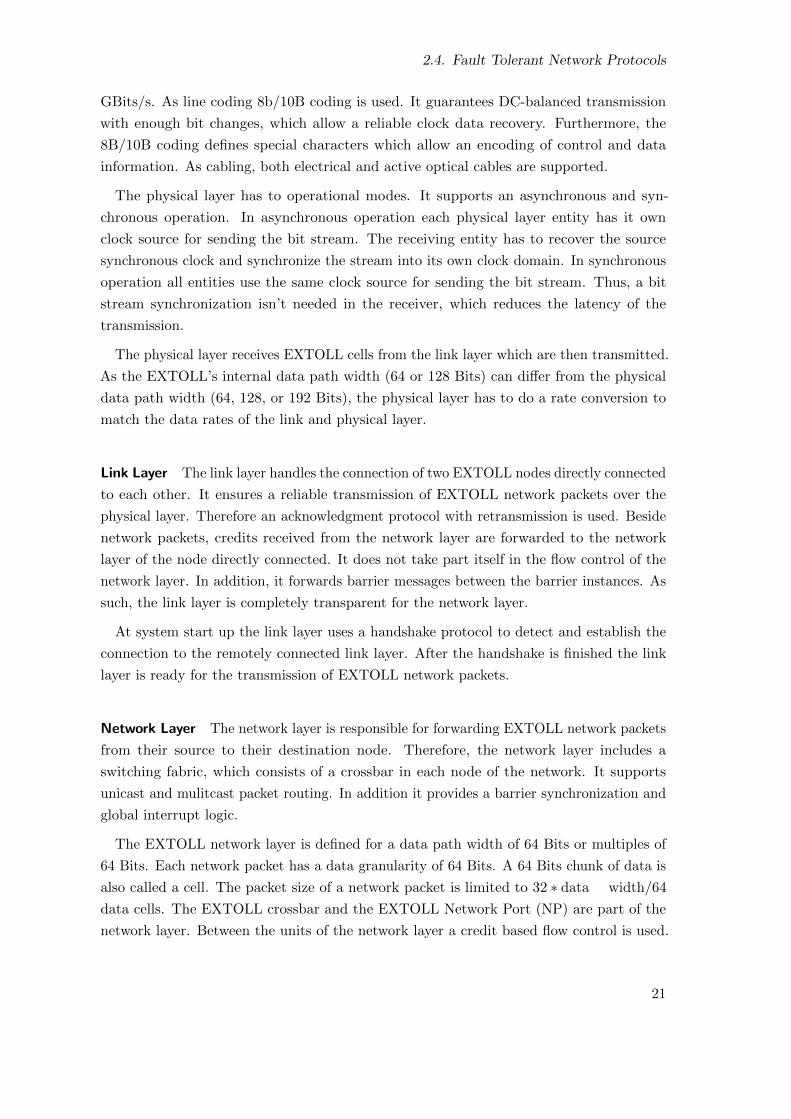
A control cell(figure 2.9 on the facing page) consists of four parts: a tag, a type field, an
information field and a CRC. The type field specifies the control cell type. The information
field transports the data of the control cell.
The format of the information field is cell type specific, and each control cell type
defines its own layout. The CRC protects the control cell against bit errors caused by the
transmission of the cell over a physical link. It is calculated from the type and the payload
field. As CRC polynomial 0x90D9 is used. This polynomial has a Hamming distance of 6
for a data word length up to 135 bits according to [25], which guarantees a detection of up
to 5 bit errors.
The tag field can be used by the physical layer to distinguish between data and control
cells. For example an 8B/10B coded physical layer can insert a K-character for the control
field. The link and network layers have to use an extra control signal to distinguish between
control and data cells.
22
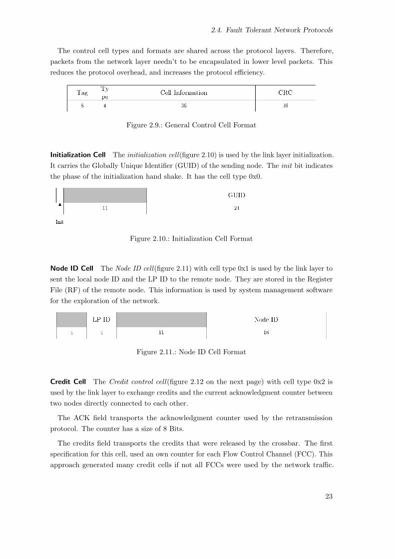
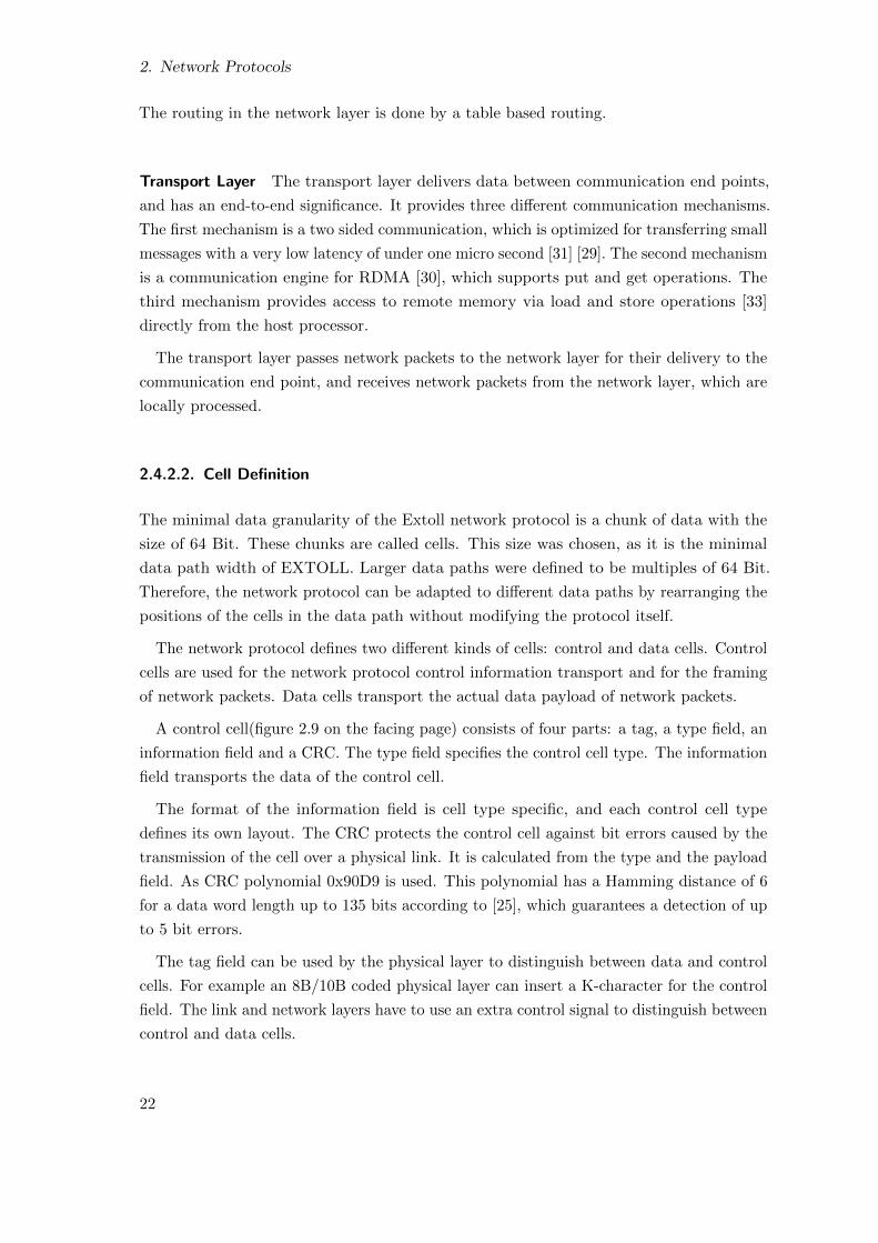
2.4. Fault Tolerant Network Protocols
The control cell types and formats are shared across the protocol layers. Therefore,
packets from the network layer needn’t to be encapsulated in lower level packets. This
reduces the protocol overhead, and increases the protocol efficiency.
Figure 2.9.: General Control Cell Format
Initialization Cell The initialization cell(figure 2.10) is used by the link layer initialization.
It carries the Globally Unique Identifier (GUID) of the sending node. The init bit indicates
the phase of the initialization hand shake. It has the cell type 0x0.
Figure 2.10.: Initialization Cell Format
Node ID Cell The Node ID cell(figure 2.11) with cell type 0x1 is used by the link layer to
sent the local node ID and the LP ID to the remote node. They are stored in the Register
File (RF) of the remote node. This information is used by system management software
for the exploration of the network.
Figure 2.11.: Node ID Cell Format
Credit Cell The Credit control cell(figure 2.12 on the next page) with cell type 0x2 is
used by the link layer to exchange credits and the current acknowledgment counter between
two nodes directly connected to each other.
The ACK field transports the acknowledgment counter used by the retransmission
protocol. The counter has a size of 8 Bits.
The credits field transports the credits that were released by the crossbar. The first
specification for this cell, used an own counter for each Flow Control Channel (FCC). This
approach generated many credit cells if not all FCCs were used by the network traffic.
23
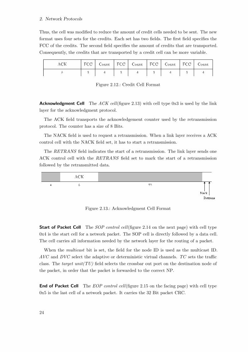
2. Network Protocols
Thus, the cell was modified to reduce the amount of credit cells needed to be sent. The new
format uses four sets for the credits. Each set has two fields. The first field specifies the
FCC of the credits. The second field specifies the amount of credits that are transported.
Consequently, the credits that are transported by a credit cell can be more variable.
Figure 2.12.: Credit Cell Format
Acknowledgment Cell The ACK cell(figure 2.13) with cell type 0x3 is used by the link
layer for the acknowledgment protocol.
The ACK field transports the acknowledgement counter used by the retransmission
protocol. The counter has a size of 8 Bits.
The NACK field is used to request a retransmission. When a link layer receives a ACK
control cell with the NACK field set, it has to start a retransmission.
The RETRANS field indicates the start of a retransmission. The link layer sends one
ACK control cell with the RETRANS field set to mark the start of a retransmission
followed by the retransmitted data.
Figure 2.13.: Acknowledgment Cell Format
Start of Packet Cell The SOP control cell(figure 2.14 on the next page) with cell type
0x4 is the start cell for a network packet. The SOP cell is directly followed by a data cell.
The cell carries all information needed by the network layer for the routing of a packet.
When the multicast bit is set, the field for the node ID is used as the multicast ID.
AVC and DVC select the adaptive or deterministic virtual channels. TC sets the traffic
class. The target unit(TU) field selects the crossbar out port on the destination node of
the packet, in order that the packet is forwarded to the correct NP.
End of Packet Cell The EOP control cell(figure 2.15 on the facing page) with cell type
0x5 is the last cell of a network packet. It carries the 32 Bit packet CRC.
24
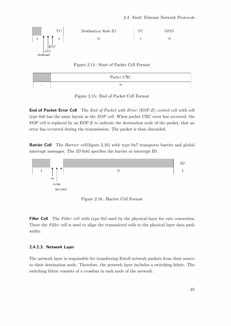
2.4. Fault Tolerant Network Protocols
Figure 2.14.: Start of Packet Cell Format
Figure 2.15.: End of Packet Cell Format
End of Packet Error Cell The End of Packet with Error (EOP E) control cell with cell
type 0x6 has the same layout as the EOP cell. When packet CRC error has occurred, the
EOP cell is replaced by an EOP E to indicate the destination node of the packet, that an
error has occurred during the transmission. The packet is than discarded.
Barrier Cell The Barrier cell(figure 2.16) with type 0x7 transports barrier and global
interrupt messages. The ID field specifies the barrier or interrupt ID.
Figure 2.16.: Barrier Cell Format
Filler Cell The Filler cell with type 0xf used by the physical layer for rate conversion.
There the Filler cell is used to align the transmitted cells to the physical layer data path
width.
2.4.2.3. Network Layer
The network layer is responsible for transferring Extoll network packets from their source
to their destination node. Therefore, the network layer includes a switching fabric. The
switching fabric consists of a crossbar in each node of the network.
25
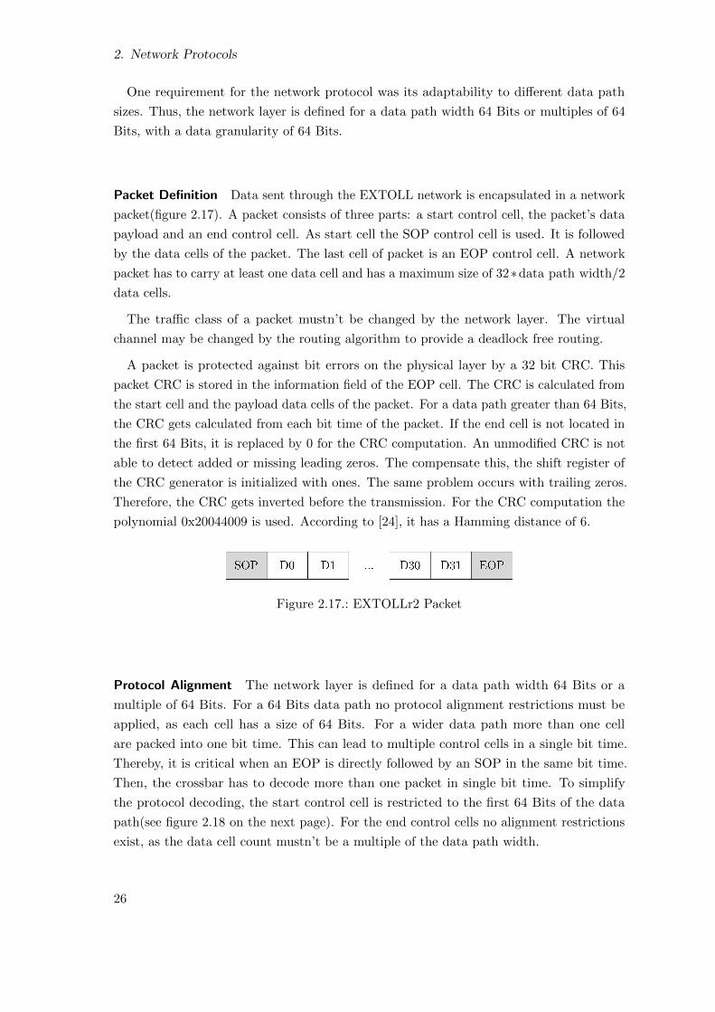
2. Network Protocols
One requirement for the network protocol was its adaptability to different data path
sizes. Thus, the network layer is defined for a data path width 64 Bits or multiples of 64
Bits, with a data granularity of 64 Bits.
Packet Definition Data sent through the EXTOLL network is encapsulated in a network
packet(figure 2.17). A packet consists of three parts: a start control cell, the packet’s data
payload and an end control cell. As start cell the SOP control cell is used. It is followed
by the data cells of the packet. The last cell of packet is an EOP control cell. A network
packet has to carry at least one data cell and has a maximum size of 32∗data path width/2
data cells.
The traffic class of a packet mustn’t be changed by the network layer. The virtual
channel may be changed by the routing algorithm to provide a deadlock free routing.
A packet is protected against bit errors on the physical layer by a 32 bit CRC. This
packet CRC is stored in the information field of the EOP cell. The CRC is calculated from
the start cell and the payload data cells of the packet. For a data path greater than 64 Bits,
the CRC gets calculated from each bit time of the packet. If the end cell is not located in
the first 64 Bits, it is replaced by 0 for the CRC computation. An unmodified CRC is not
able to detect added or missing leading zeros. The compensate this, the shift register of
the CRC generator is initialized with ones. The same problem occurs with trailing zeros.
Therefore, the CRC gets inverted before the transmission. For the CRC computation the
polynomial 0x20044009 is used. According to [24], it has a Hamming distance of 6.
Figure 2.17.: EXTOLLr2 Packet
Protocol Alignment The network layer is defined for a data path width 64 Bits or a
multiple of 64 Bits. For a 64 Bits data path no protocol alignment restrictions must be
applied, as each cell has a size of 64 Bits. For a wider data path more than one cell
are packed into one bit time. This can lead to multiple control cells in a single bit time.
Thereby, it is critical when an EOP is directly followed by an SOP in the same bit time.
Then, the crossbar has to decode more than one packet in single bit time. To simplify
the protocol decoding, the start control cell is restricted to the first 64 Bits of the data
path(see figure 2.18 on the next page). For the end control cells no alignment restrictions
exist, as the data cell count mustn’t be a multiple of the data path width.
26
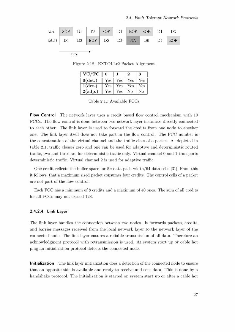
2.4. Fault Tolerant Network Protocols
Figure 2.18.: EXTOLLr2 Packet Alignment
VC/TC 0 1 2 3
0(det.) Yes Yes Yes Yes
1(det.) Yes Yes Yes Yes
2(adp.) Yes Yes No No
Table 2.1.: Available FCCs
Flow Control The network layer uses a credit based flow control mechanism with 10
FCCs. The flow control is done between two network layer instances directly connected
to each other. The link layer is used to forward the credits from one node to another
one. The link layer itself does not take part in the flow control. The FCC number is
the concatenation of the virtual channel and the traffic class of a packet. As depicted in
table 2.1, traffic classes zero and one can be used for adaptive and deterministic routed
traffic, two and three are for deterministic traffic only. Virtual channel 0 and 1 transports
deterministic traffic. Virtual channel 2 is used for adaptive traffic.
One credit reflects the buffer space for 8 ∗ data path width/64 data cells [31]. From this
it follows, that a maximum sized packet consumes four credits. The control cells of a packet
are not part of the flow control.
Each FCC has a minimum of 8 credits and a maximum of 40 ones. The sum of all credits
for all FCCs may not exceed 128.
2.4.2.4. Link Layer
The link layer handles the connection between two nodes. It forwards packets, credits,
and barrier messages received from the local network layer to the network layer of the
connected node. The link layer ensures a reliable transmission of all data. Therefore an
acknowledgment protocol with retransmission is used. At system start up or cable hot
plug an initialization protocol detects the connected node.
Initialization The link layer initialization does a detection of the connected node to ensure
that an opposite side is available and ready to receive and sent data. This is done by a
handshake protocol. The initialization is started on system start up or after a cable hot
27
2. Network Protocols
plug.
The handshake consists of two phases. In the first phase a beacon message is sent to
signal its own availability. In in the second phase a reply message is transmitted to inform
the opposite side, that its beacon has been received. Afterward, the link is established and
fully operational.
The initialization state machine is depicted in figure 2.19 on the next page. The
initialization sequence uses initialization control cells for the information exchange. First,
each layer sends an initialization cell with the init field set to zero. Then, it waits for the
reception of an initialization cell. If such a cell is not received within 1ms, the initialization
cell is sent again. If it receives an initialization cell with init set to zero, it confirms the
reception by sending an initialization cell with init set to one, and the handshake is done
for this node. If it receives an initialization cell with init set to one, then the opposite has
already finished the handshake, which means, that the handshake can also be ended for
this node.
Afterward, a Node ID cell is sent, which carries the node ID and the LP ID sending LP.
This information is stored in the RF of the receiving node, and it is used by the system
management software for the exploration of the network.
The link layer returns to the link down state any time the physical layer indicates, that
it has lost the connection, or in the ready state and an init cell is received. Then, the
initialization is restarted as soon as the physical layer reports its readiness.
Retransmission Protocol A retransmission protocol can be used two guarantee the
reliable transmission of data in an interconnection network. Thereby, the sender stores the
data in a buffer, when it sends the data. The receiver of the data acknowledges the correct
reception by returning a reply message. Upon the reception of the reply message, the
sender removes the data from its retransmission buffer. A retransmission can be requested
either by sending a reply message stating, that the data was corrupted, or be omitting the
reply. Then, a timeout has to be used to resend the data.
Generally, there are two possibilities to realize a retransmission protocol. The first
option is to use an end to end retransmission. There the source node stores the data in
a retransmission buffer, and the destination node generates the reply. When the data
is corrupted in an intermediate hop, it is discarded and a timeout in the source node is
used the start the retransmission. This method has several drawbacks. The size of the
retransmission buffer and the amount of outstanding packets limit the scalability of the
network, as buffer space must be available for each data sent. When the network size
grows, more data is on the fly in the network. Therefore, also the buffers have to grow,
which is not practical for large networks and buffers. Furthermore, a retransmission needs
28
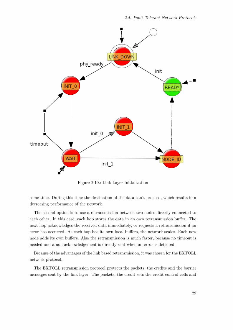
2.4. Fault Tolerant Network Protocols
Figure 2.19.: Link Layer Initialization
some time. During this time the destination of the data can’t proceed, which results in a
decreasing performance of the network.
The second option is to use a retransmission between two nodes directly connected to
each other. In this case, each hop stores the data in an own retransmission buffer. The
next hop acknowledges the received data immediately, or requests a retransmission if an
error has occurred. As each hop has its own local buffers, the network scales. Each new
node adds its own buffers. Also the retransmission is much faster, because no timeout is
needed and a non acknowledgement is directly sent when an error is detected.
Because of the advantages of the link based retransmission, it was chosen for the EXTOLL
network protocol.
The EXTOLL retransmission protocol protects the packets, the credits and the barrier
messages sent by the link layer. The packets, the credit sets the credit control cells and
29
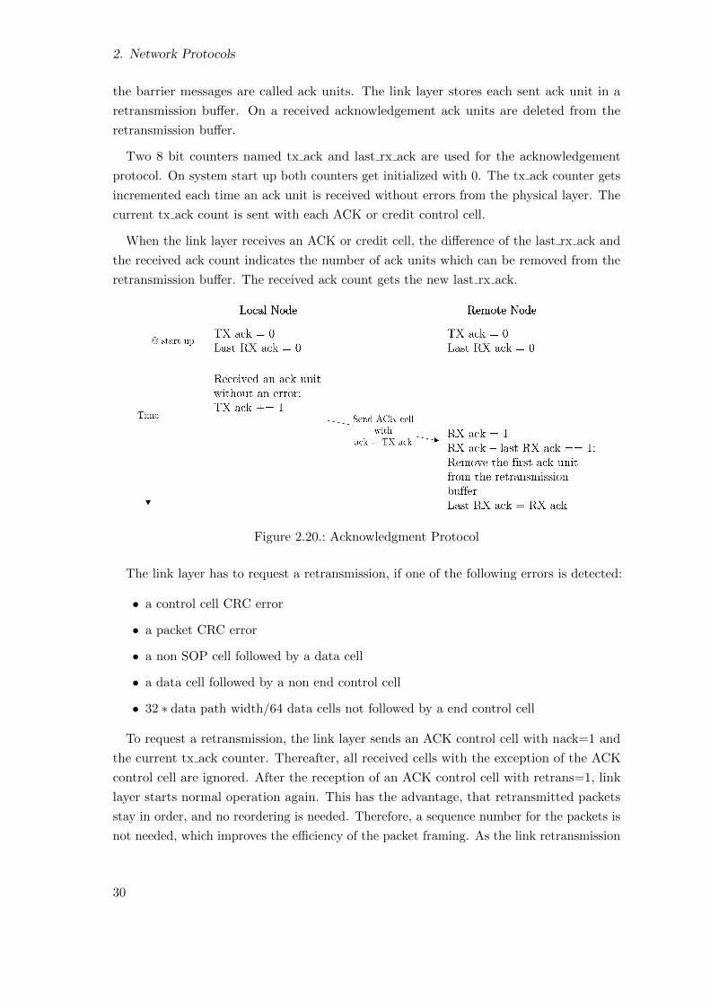
2. Network Protocols
the barrier messages are called ack units. The link layer stores each sent ack unit in a
retransmission buffer. On a received acknowledgement ack units are deleted from the
retransmission buffer.
Two 8 bit counters named tx ack and last rx ack are used for the acknowledgement
protocol. On system start up both counters get initialized with 0. The tx ack counter gets
incremented each time an ack unit is received without errors from the physical layer. The
current tx ack count is sent with each ACK or credit control cell.
When the link layer receives an ACK or credit cell, the difference of the last rx ack and
the received ack count indicates the number of ack units which can be removed from the
retransmission buffer. The received ack count gets the new last rx ack.
Figure 2.20.: Acknowledgment Protocol
The link layer has to request a retransmission, if one of the following errors is detected:
• a control cell CRC error
• a packet CRC error
• a non SOP cell followed by a data cell
• a data cell followed by a non end control cell
• 32 ∗ data path width/64 data cells not followed by a end control cell
To request a retransmission, the link layer sends an ACK control cell with nack=1 and
the current tx ack counter. Thereafter, all received cells with the exception of the ACK
control cell are ignored. After the reception of an ACK control cell with retrans=1, link
layer starts normal operation again. This has the advantage, that retransmitted packets
stay in order, and no reordering is needed. Therefore, a sequence number for the packets is
not needed, which improves the efficiency of the packet framing. As the link retransmission
30
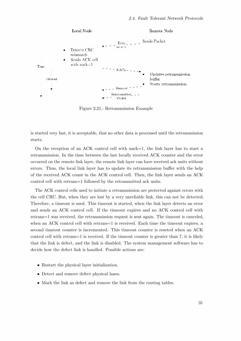
2.4. Fault Tolerant Network Protocols
Figure 2.21.: Retransmission Example
is started very fast, it is acceptable, that no other data is processed until the retransmission
starts.
On the reception of an ACK control cell with nack=1, the link layer has to start a
retransmission. In the time between the last locally received ACK counter and the error
occurred on the remote link layer, the remote link layer can have received ack units without
errors. Thus, the local link layer has to update its retransmission buffer with the help
of the received ACK count in the ACK control cell. Then, the link layer sends an ACK
control cell with retrans=1 followed by the retransmitted ack units.
The ACK control cells used to initiate a retransmission are protected against errors with
the cell CRC. But, when they are lost by a very unreliable link, this can not be detected.
Therefore, a timeout is used. This timeout is started, when the link layer detects an error
and sends an ACK control cell. If the timeout expires and no ACK control cell with
retrans=1 was received, the retransmission request is sent again. The timeout is canceled,
when an ACK control cell with retrans=1 is received. Each time the timeout expires, a
second timeout counter is incremented. This timeout counter is reseted when an ACK
control cell with retrans=1 is received. If the timeout counter is greater than 7, it is likely
that the link is defect, and the link is disabled. The system management software has to
decide how the defect link is handled. Possible actions are:
• Restart the physical layer initialization.
• Detect and remove defect physical lanes.
• Mark the link as defect and remove the link from the routing tables.
31

2. Network Protocols
2.4.2.5. Protocol Analysis
Each network packet has as framing an SOP cell and an EOP cell. As each cell has a size
of 8 Bytes, and therefore a 16 Bytes are needed for the framing of packet. To send an
RMA put request, the RMA adds a command header of 16 Bytes into the payload of the
packet before the actual transmitted data. Therefore, the protocol has an efficiency of 88%
for an RDMA put request. A two sided Virtualized Engine for Low Overhead (VELO)
message has a command header of 8 Bytes, and therefore a protocol efficiency of 91%.
Due to the protocol granularity of 64 Bits and the use of cells, is the protocol easily
adaptable the different data path sizes by distributing the cells over the data path. The
SOP alignment guarantees a simple decoding of received packets in all network layers.
The high reliability of the network protocol is reached by the use of strong CRCs to
protect all parts of the protocol. All control cells are protected by an own CRC. Thus,
the link layer can ensure to forward only packets to the network with a correct routing
information, which eliminates falsely routed packets. Furthermore, credits and barrier
messages are now protected by the retransmission, as well as the packet data, which is
protected by a 32 Bits CRC. In contrast to the network protocol for EXTOLLr1, the
retransmission itself is protected against errors. This is reached by the use of timeouts for
sent ack cells.
32
3. Barrier Synchronization
Computer systems used in HPC consist of hundreds to thousands compute nodes. On these
systems, a program is executed in parallel on the compute nodes. Typically, such programs
solve a computational problem iteratively. First, the data needed for the computation
is distributed among the compute nodes. Thereafter, they start the computation. To
fulfill this task, intermediate results and data must be exchanged during the computation.
Therefore, the compute nodes must wait after a computational iteration, until all other
nodes have reached the same synchronization point as well. When all nodes have reached
the synchronization point, the data for the next iteration is exchanged, and the nodes
resume the computation. The need for a regular synchronization is tightened by a possible
unbalance of the computational execution time or unbalanced data structures. The problem
of an unbalanced computational execution time is partly caused by Operation System (OS)
jitter [34]. This jitter has its origin in timer interrupts and different OS daemons, that are
executed on the compute nodes. When they are executed, the computation is stopped,
until they are finished.
The described synchronization is done with the help of a collective operation called
barrier [35]. At defined synchronization points, all processes of a parallel program wait until
all other processes also have arrived at the synchronization point. This synchronization
point is called a barrier. After all processes have reached the barrier, they can proceed with
their execution. During the time needed for the synchronization, the parallel program can
not make any progress. Therefore, it is essential to have an efficient barrier implementation,
that reduces the time needed for the operation. As the barrier operation is critical for
parallel programs, several proposals were made for hardware barrier implementations in
the past ([36], [37], [38], [39]).
This section will propose a new way to integrate a barrier synchronization directly into
an interconnection network, which improves the performance of the barrier operation
significantly. Furthermore, the proposed barrier implementation is extended to support a
global interrupt mechanism, that can be used to reduce the OS jitter.
33
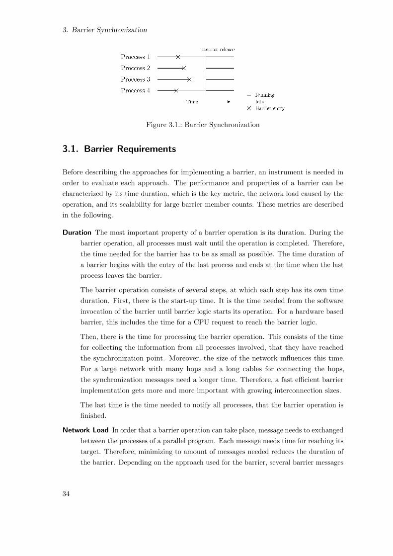
3. Barrier Synchronization
Figure 3.1.: Barrier Synchronization
3.1. Barrier Requirements
Before describing the approaches for implementing a barrier, an instrument is needed in
order to evaluate each approach. The performance and properties of a barrier can be
characterized by its time duration, which is the key metric, the network load caused by the
operation, and its scalability for large barrier member counts. These metrics are described
in the following.
Duration The most important property of a barrier operation is its duration. During the
barrier operation, all processes must wait until the operation is completed. Therefore,
the time needed for the barrier has to be as small as possible. The time duration of
a barrier begins with the entry of the last process and ends at the time when the last
process leaves the barrier.
The barrier operation consists of several steps, at which each step has its own time
duration. First, there is the start-up time. It is the time needed from the software
invocation of the barrier until barrier logic starts its operation. For a hardware based
barrier, this includes the time for a CPU request to reach the barrier logic.
Then, there is the time for processing the barrier operation. This consists of the time
for collecting the information from all processes involved, that they have reached
the synchronization point. Moreover, the size of the network influences this time.
For a large network with many hops and a long cables for connecting the hops,
the synchronization messages need a longer time. Therefore, a fast efficient barrier
implementation gets more and more important with growing interconnection sizes.
The last time is the time needed to notify all processes, that the barrier operation is
finished.
Network Load In order that a barrier operation can take place, message needs to exchanged
between the processes of a parallel program. Each message needs time for reaching its
target. Therefore, minimizing to amount of messages needed reduces the duration of
the barrier. Depending on the approach used for the barrier, several barrier messages
34
3.2. Barrier Design Space Evaluation
must be combined in a single place. Thus, a bottleneck can occur, when many
messages hit the same target.
Furthermore, several different parallel programs can be executed on a parallel system
at the same time. Programs, which do not take part in a barrier operation, also
exchange message. Consequently, these messages compete with the barrier messages
for the resources of the used interconnection network. This can decrease the latency
of barrier message in a saturated network. For that reason, a smaller network load of
a barrier operation can improve the overall performance of a barrier operation.
Scalability The scalability of a system describes its ability to improve its performance, when
new components are added. Thereby, the performance gain should be proportional
with the added components. For a barrier operation, scalability is given when adding
hosts to the barrier group will not decrease the time duration significantly.
Fault Tolerance A barrier operation needs to exchange synchronize messages. These
messages are transported to its destination by an interconnection network. Especially
in large interconnection networks, the fault tolerance is getting an issue for the
reliability of a system. Mechanisms as retransmission protocols are used to ensure
a reliable transmission. The barrier operation is also affected by these mechanisms.
Barrier message need to be protected by these mechanisms, as well as it has to be
taken account of barrier messages, when designing them, to make sure that barrier
messages are not slowed down by the fault tolerance mechanisms.
3.2. Barrier Design Space Evaluation
The barrier operation can be either implemented in software or with specialized hardware.
Obviously, efficient hardware implementation should be faster than software implementa-
tions. Nevertheless, for the sake of completeness both options are described in the following
sections.
3.2.1. Software Barrier
A software barrier does not directly dependent on the used interconnection network. Of
course, an efficient interconnection network improves the performance of a software barrier.
But generally, a software barrier is used, when the interconnection network has no extra
functionality for barrier synchronization or the hardware barrier resources are consumed
by other programs.
35
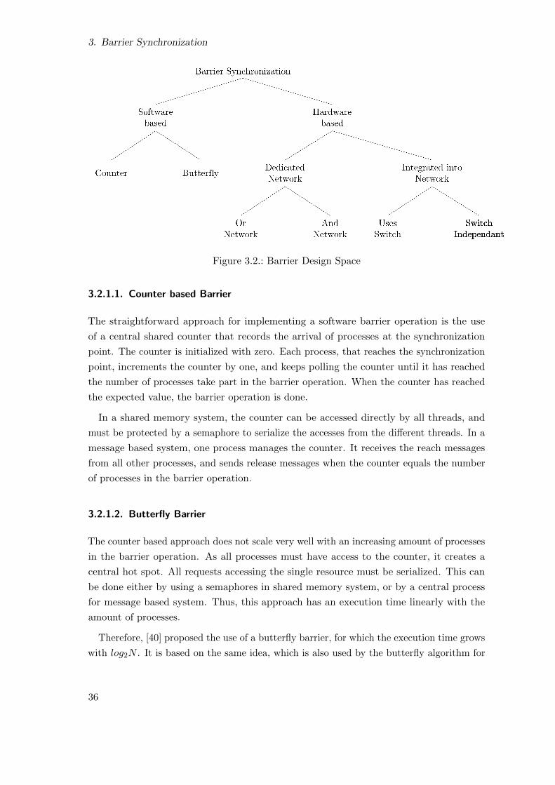
3. Barrier Synchronization
Figure 3.2.: Barrier Design Space
3.2.1.1. Counter based Barrier
The straightforward approach for implementing a software barrier operation is the use
of a central shared counter that records the arrival of processes at the synchronization
point. The counter is initialized with zero. Each process, that reaches the synchronization
point, increments the counter by one, and keeps polling the counter until it has reached
the number of processes take part in the barrier operation. When the counter has reached
the expected value, the barrier operation is done.
In a shared memory system, the counter can be accessed directly by all threads, and
must be protected by a semaphore to serialize the accesses from the different threads. In a
message based system, one process manages the counter. It receives the reach messages
from all other processes, and sends release messages when the counter equals the number
of processes in the barrier operation.
3.2.1.2. Butterfly Barrier
The counter based approach does not scale very well with an increasing amount of processes
in the barrier operation. As all processes must have access to the counter, it creates a
central hot spot. All requests accessing the single resource must be serialized. This can
be done either by using a semaphores in shared memory system, or by a central process
for message based system. Thus, this approach has an execution time linearly with the
amount of processes.
Therefore, [40] proposed the use of a butterfly barrier, for which the execution time grows
with log2N . It is based on the same idea, which is also used by the butterfly algorithm for
36
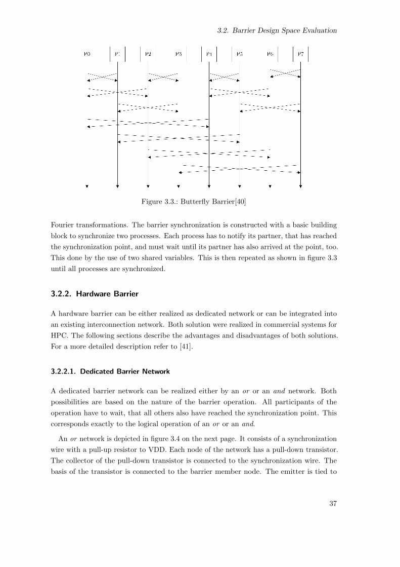
3.2. Barrier Design Space Evaluation
Figure 3.3.: Butterfly Barrier[40]
Fourier transformations. The barrier synchronization is constructed with a basic building
block to synchronize two processes. Each process has to notify its partner, that has reached
the synchronization point, and must wait until its partner has also arrived at the point, too.
This done by the use of two shared variables. This is then repeated as shown in figure 3.3
until all processes are synchronized.
3.2.2. Hardware Barrier
A hardware barrier can be either realized as dedicated network or can be integrated into
an existing interconnection network. Both solution were realized in commercial systems for
HPC. The following sections describe the advantages and disadvantages of both solutions.
For a more detailed description refer to [41].
3.2.2.1. Dedicated Barrier Network
A dedicated barrier network can be realized either by an or or an and network. Both
possibilities are based on the nature of the barrier operation. All participants of the
operation have to wait, that all others also have reached the synchronization point. This
corresponds exactly to the logical operation of an or or an and.
An or network is depicted in figure 3.4 on the next page. It consists of a synchronization
wire with a pull-up resistor to VDD. Each node of the network has a pull-down transistor.
The collector of the pull-down transistor is connected to the synchronization wire. The
basis of the transistor is connected to the barrier member node. The emitter is tied to
37
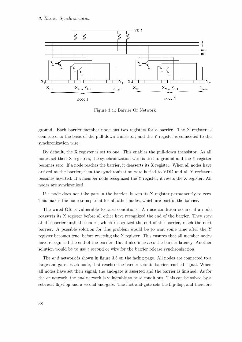
3. Barrier Synchronization
Figure 3.4.: Barrier Or Network
ground. Each barrier member node has two registers for a barrier. The X register is
connected to the basis of the pull-down transistor, and the Y register is connected to the
synchronization wire.
By default, the X register is set to one. This enables the pull-down transistor. As all
nodes set their X registers, the synchronization wire is tied to ground and the Y register
becomes zero. If a node reaches the barrier, it deasserts its X register. When all nodes have
arrived at the barrier, then the synchronization wire is tied to VDD and all Y registers
becomes asserted. If a member node recognized the Y register, it resets the X register. All
nodes are synchronized.
If a node does not take part in the barrier, it sets its X register permanently to zero.
This makes the node transparent for all other nodes, which are part of the barrier.
The wired-OR is vulnerable to raise conditions. A raise condition occurs, if a node
reasserts its X register before all other have recognized the end of the barrier. They stay
at the barrier until the nodes, which recognized the end of the barrier, reach the next
barrier. A possible solution for this problem would be to wait some time after the Y
register becomes true, before resetting the X register. This ensures that all member nodes
have recognized the end of the barrier. But it also increases the barrier latency. Another
solution would be to use a second or wire for the barrier release synchronization.
The and network is shown in figure 3.5 on the facing page. All nodes are connected to a
large and gate. Each node, that reaches the barrier sets its barrier reached signal. When
all nodes have set their signal, the and-gate is asserted and the barrier is finished. As for
the or network, the and network is vulnerable to raise conditions. This can be solved by a
set-reset flip-flop and a second and-gate. The first and-gate sets the flip-flop, and therefore
38

3.2. Barrier Design Space Evaluation
Figure 3.5.: Barrier And Network
the barrier done signal. When node as noticed the barrier done signal, it sets the signal to
the second and-gate. This way, barrier done signal is not reset not until all nodes have
acknowledged the barrier done signal.
The advantage of the described dedicated networks, is their performance for the barrier
operation. On the other hand a second network beside the main interconnection network
is needed, which is very cost intensive.
3.2.2.2. Integrated Barrier Network
As a dedicated barrier network are very cost intensive, modern interconnection networks
integrate the barrier functionality into the same network, which is also used for the main
data transport. Thereby, the same algorithms are used as for software barriers. In contrast
to software barriers, the synchronization variables are not located in the main memory, but
in a special barrier logic in the network. Therefore, the hardware barrier is much faster, as
the barrier logic has not to access main memory in each hop.
An integrated barrier is realized in two phases. In the first phase the information from
all nodes is collected, that they have reached the synchronization point. This phase is
called the up phase. In the second phase all nodes are notified about the end of the barrier.
This phase is called the down phase.
An interconnection network consists of multiple switching stages. For the hardware
barrier, these stages are organized in a virtual tree structure. The nodes of this tree
represent the participating network nodes of the barrier. The processing of the barrier
starts in the leave nodes. When a leave nodes reaches the barrier, it sends an up message
to its parent node. All other nodes of the tree, waits until the own node and all child nodes
have reached the barrier. Then, they send an up message to their parent node as well.
This is repeated until the root node has reached the barrier and received up messages from
all child nodes. At this point all nodes have reached the barrier. Thereafter, the root node
sends down messages to its child nodes, which are then propagated to the leave nodes.
When node receives a down message, it ends the barrier operation.
[41] gives a further description about the integration of a hardware barrier into an
interconnection network.
39
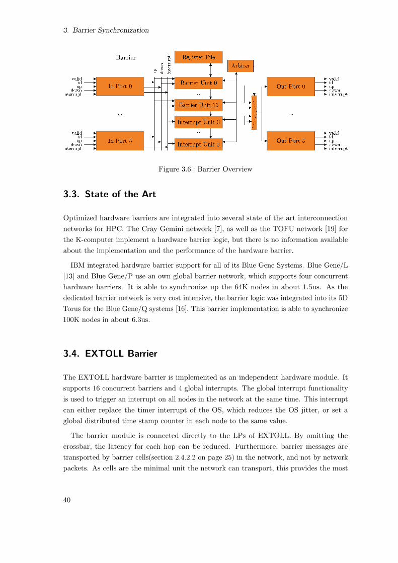
3. Barrier Synchronization
Figure 3.6.: Barrier Overview
3.3. State of the Art
Optimized hardware barriers are integrated into several state of the art interconnection
networks for HPC. The Cray Gemini network [7], as well as the TOFU network [19] for
the K-computer implement a hardware barrier logic, but there is no information available
about the implementation and the performance of the hardware barrier.
IBM integrated hardware barrier support for all of its Blue Gene Systems. Blue Gene/L
[13] and Blue Gene/P use an own global barrier network, which supports four concurrent
hardware barriers. It is able to synchronize up the 64K nodes in about 1.5us. As the
dedicated barrier network is very cost intensive, the barrier logic was integrated into its 5D
Torus for the Blue Gene/Q systems [16]. This barrier implementation is able to synchronize
100K nodes in about 6.3us.
3.4. EXTOLL Barrier
The EXTOLL hardware barrier is implemented as an independent hardware module. It
supports 16 concurrent barriers and 4 global interrupts. The global interrupt functionality
is used to trigger an interrupt on all nodes in the network at the same time. This interrupt
can either replace the timer interrupt of the OS, which reduces the OS jitter, or set a
global distributed time stamp counter in each node to the same value.
The barrier module is connected directly to the LPs of EXTOLL. By omitting the
crossbar, the latency for each hop can be reduced. Furthermore, barrier messages are
transported by barrier cells(section 2.4.2.2 on page 25) in the network, and not by network
packets. As cells are the minimal unit the network can transport, this provides the most
40
3.4. EXTOLL Barrier
efficient way to forward barrier messages. The barrier cell carries the barrier ID and a flag,
which indicates if it is an up, down, or interrupt messages.
The LP arbitrates the link between barrier messages and network packets. Thereby,
barrier messages have a higher priority than network messages, which guarantees a fast
barrier operation even for saturated networks. For interrupt messages it is important,
that they have constant latency, when they traverse a hop. Only then, it is possible to
deliver the interrupt in all nodes at the same time. Therefore, global interrupt messages
are handled by the LP using delayed insertion. As each packet has a maximum length of
34 clock cycles, the LP delays each interrupt message received from the barrier module
for 34 clock cycles. In the meantime, if there is a packet in process, this packet is sent
completely, but no more packet are granted the link until the interrupt message is sent.
This guarantees a constant latency in each hop.
The barrier module is depicted in figure 3.6 on the facing page. The In Ports are
connected to the LPs, and forward received barrier messages to the according barrier or
interrupt unit based on the ID of the message. Each barrier unit consists of three sets of
registers. The first set is used for the configuration. These registers are set by management
software with the help of the RF. As all nodes part of a barrier ID are arranged in a virtual
tree structure, they configure which link leads to the parent node, and which ones to the
child nodes. Furthermore, they configure if the local node and when how many processes
of the local node are part of the barrier. This way, several process on single node can
take part in a barrier by notifying the hardware directly when they reached the barrier
without any further synchronization on the local node, which lowers the duration time of
the barrier.
The second set of registers is the interaction set for each ID. It is used by processes
of the local node to interact with the barrier logic. It consists of reached and released
registers. These registers are mapped into the address space of a process part of the barrier.
A process writes the reached register, when it has arrived at the synchronization point.
Thereafter, it polls the released register, which is set by the barrier logic in the release
phase of the barrier, and gets reset the next time the reached register is written. A raise
condition can occur, when more than one process on a node are part of a barrier ID, and
trigger the barrier in short intervals. Then, a process can read the released register and
write the reached one, before all other processes have noticed the release of the previous
barrier. To avoid the raise condition, the released register was duplicated. These two
registers are used alternately. For the first barrier, the first released register is used, and
after each barrier the active released register is changed. A status bit in the barrier RF
states for each barrier ID, which is the current active released register.
The third set of registers is the working set, which holds the current status of the barrier.
41

3. Barrier Synchronization
It consists of a host counter, a bit mask for each link, and a phase marker. The counter is
incremented each time the reached register of the interaction set is written, and is reset in
the down phase. The bits of the mask are set for the corresponding link in the up phase,
when a barrier message is received from a LP. When the host counter has reached the
value specified in the configuration set, and all up messages were received from all child
nodes, the barrier unit sends an up message to its parent node, if the current node is not
the root node of the barrier tree. If the current node is the root node, which is indicated
by a not set parent node in the configuration set, the barrier unit sends down messages to
all child nodes, and sets the active released bit in the interaction set. When a barrier unit
receives a down message, it is forwarded to all configured child nodes. Additionally, the
active released bit is set, if the host count for the current node is not zero.
A barrier unit needs to send all messages for a phase at the same time. Therefore, an
arbiter is used to handle the access to the barrier out ports. A barrier units requests the
out ports, and on a grant the barrier message is sent to all ports leading to child nodes in
the down phase, or to the parent node in the up phase. The out ports are connected the
LPs.
The interrupt units are used for processing the global interrupts. Global interrupts are
distributed from a root node to all other nodes, on which the interrupt should be triggered.
Therefore, the same virtual tree structure is used as for the barrier. As the interrupt units
have to distribute the interrupt without collecting information before, they use the same
logic function as the barrier unit uses for the down phase. Consequently, its configuration
registers indicate, which links lead to the child nodes of a node.
A global interrupt has to be triggered on all nodes at the same time. As the interrupt
messages propagate from the root node to the child nodes through the network like a wave,
the interrupt is triggered earlier on the root node than on the child nodes. To compensate
this, a delay counter was introduced in the interrupt unit. The counter is started when
an interrupt message is received and triggers the local interrupt when it exceeds a value
specified in the configuration registers. The value has to be larger for nodes next to the
root node, and is zero for the leave nodes. To be able to adjust the delay cois wayters,
a measurement logic was integrated into the interrupt unit, which measures the time an
interrupt messages needs to traverse a single link. The logic consists of a counter, which is
accessible by the RF. A measurement is done by sending an interrupt message to another
node directly connected, which reflects the interrupt message. The counter is reset and
started when the start node sends the measurement message, and stopped, when the
reflected message is received. The reflection is done by configuring the sending node as the
single child node in the remote node. This way, all links that are used by an interrupt tree
can be exactly measured. Thereafter, all delay counters are set with the values received
from the measurements.
42
3.4. EXTOLL Barrier
3.4.1. Performance Evaluation
The barrier module was implemented in a Verilog Register Transfer Level (RTL) description.
This implementation was verified using formal verification. From the simulation, the
performance of the implementation was extracted. A barrier message needs 5 clock cycles
for passing the barrier module. Furthermore, the LP needs 6 clock cycles for sending a
message to link and 11 clock cycles for passing a received message from the link to the
barrier module. The physical layer needs about 10 clock cycles for transmitting a cell.
Thus, a barrier message needs 32 clock cycles for a single hop. A 3D Torus network with
216 nodes has diameter of 32( 3√N − 1) = 59. Therefore, about 1900 clock cycles are needed
by an up message to traverse the network from the leave nodes to the root node, and
3800 clock cycles for a complete barrier operation. Assuming a frequency of 750 MHz for
EXTOLL, a 216 nodes cluster can be synchronized in about 5us.
The barrier implementation was tested on a test cluster with nine nodes. Each node was
equipped with an Opteron CPU running at 1600 MHz, and an Ventoux FPGA card. The
FPGA board was connected to CPU via HyperTransport (HT), and were loaded with a
complete EXTOLL design including the barrier module. The EXTOLL logic run at 200
MHz. Beside EXTOLL, the cluster was also equipped with a Gigabit Ethernet network.
A small test program was written to measure the performance of the hardware barrier.
This program executed the barrier operation repeatedly. The measurements were done
using a Message Passing Interface (MPI) barrier with Ethernet and with EXTOLL. The
measurements for the hardware barrier were done without MPI. The barrier operation
synchronizing the nine nodes took 160us using Ethernet, 4,5us using EXTOLL with two
sided communication, and 1,2us using the hardware barrier.
43

3. Barrier Synchronization
44
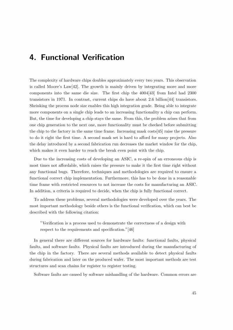
4. Functional Verification
The complexity of hardware chips doubles approximately every two years. This observation
is called Moore’s Law[42]. The growth is mainly driven by integrating more and more
components into the same die size. The first chip the 4004[43] from Intel had 2300
transistors in 1971. In contrast, current chips do have about 2.6 billion[44] transistors.
Shrinking the process node size enables this high integration grade. Being able to integrate
more components on a single chip leads to an increasing functionality a chip can perform.
But, the time for developing a chip stays the same. From this, the problem arises that from
one chip generation to the next one, more functionality must be checked before submitting
the chip to the factory in the same time frame. Increasing mask costs[45] raise the pressure
to do it right the first time. A second mask set is hard to afford for many projects. Also
the delay introduced by a second fabrication run decreases the market window for the chip,
which makes it even harder to reach the break even point with the chip.
Due to the increasing costs of developing an ASIC, a re-spin of an erroneous chip is
most times not affordable, which raises the pressure to make it the first time right without
any functional bugs. Therefore, techniques and methodologies are required to ensure a
functional correct chip implementation. Furthermore, this has to be done in a reasonable
time frame with restricted resources to not increase the costs for manufacturing an ASIC.
In addition, a criteria is required to decide, when the chip is fully functional correct.
To address these problems, several methodologies were developed over the years. The
most important methodology beside others is the functional verification, which can best be
described with the following citation:
”Verification is a process used to demonstrate the correctness of a design with
respect to the requirements and specification.”[46]
In general there are different sources for hardware faults: functional faults, physical
faults, and software faults. Physical faults are introduced during the manufacturing of
the chip in the factory. There are several methods available to detect physical faults
during fabrication and later on the produced wafer. The most important methods are test
structures and scan chains for register to register testing.
Software faults are caused by software mishandling of the hardware. Common errors are
45

4. Functional Verification
Figure 4.1.: Verification Reconvergence Model
writing to a wrong register or writing the wrong data to the right register. Software faults
are hard to detect as it is difficult to distinguish who caused the fault, the hardware or the
software. Once detected they can be fixed in a short time frame. Even when the hardware
is already in production and shipped to the customer.
Functional faults have their origin in the specification or the implementation of a chip.
The chip design process starts by defining a specification. The specification is a text
document written in natural language which describes the chip to be implemented. It
includes the function the chip has to perform, the interfaces to the outside world, and the
conditions that affect the design. After the specification is finished, the chip design team
starts to implemented the design in RTL. The specification and the implemented RTL
are two representations of the chip. As the transformation into RTL is done by humans,
it is fault-prone. Beside errors made during this transformation, specifications can be
wrong, vague, or not existing. As the specification is written in natural language, it is
hard to describe the features exactly as intended. This leads to an interpretation of the
specification from the RTL designer. This interpretation can obviously be different from
the intention of the specification.
To model this relationship [46] defines the reconvergence model as depicted in figure 4.1.
It is an illustration of the verification process. On the one hand there is the transformation
from the specification to RTL which also called implementation. On the other hand there is
the verification. The verification ensures that the RTL matches the specification. Therefore,
the verification introduces a second path. This second path compares the RTL against
the specification. When both paths are independent from each other, than the verification
process can be successful. This verification process can be used between any two different
design representations. As mentioned before, between the specification and RTL. But also
between RTL and the gate level netlist after synthesis. Depending on the transformation
different verification techniques can be used. These are described in a later section.
The interpretation of the specification is a big problem in the verification process. Espe-
cially when the implementation and the verification are based on the same interpretation as
shown in figure 4.2 on the facing page. Then the chip seems to be verified, but on the wrong
assumptions, as the functionality of the chip does not corresponds to the specification.
For a successful verification process the human intervention and other error sources must
46
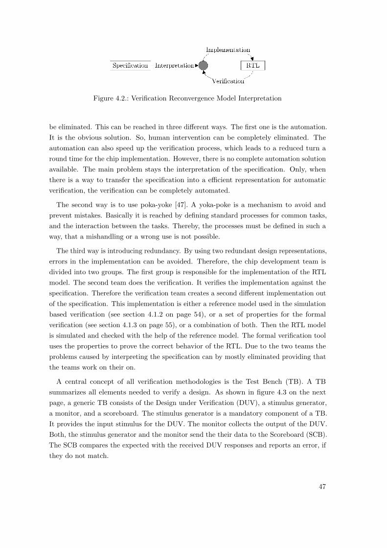
Figure 4.2.: Verification Reconvergence Model Interpretation
be eliminated. This can be reached in three different ways. The first one is the automation.
It is the obvious solution. So, human intervention can be completely eliminated. The
automation can also speed up the verification process, which leads to a reduced turn a
round time for the chip implementation. However, there is no complete automation solution
available. The main problem stays the interpretation of the specification. Only, when
there is a way to transfer the specification into a efficient representation for automatic
verification, the verification can be completely automated.
The second way is to use poka-yoke [47]. A yoka-poke is a mechanism to avoid and
prevent mistakes. Basically it is reached by defining standard processes for common tasks,
and the interaction between the tasks. Thereby, the processes must be defined in such a
way, that a mishandling or a wrong use is not possible.
The third way is introducing redundancy. By using two redundant design representations,
errors in the implementation can be avoided. Therefore, the chip development team is
divided into two groups. The first group is responsible for the implementation of the RTL
model. The second team does the verification. It verifies the implementation against the
specification. Therefore the verification team creates a second different implementation out
of the specification. This implementation is either a reference model used in the simulation
based verification (see section 4.1.2 on page 54), or a set of properties for the formal
verification (see section 4.1.3 on page 55), or a combination of both. Then the RTL model
is simulated and checked with the help of the reference model. The formal verification tool
uses the properties to prove the correct behavior of the RTL. Due to the two teams the
problems caused by interpreting the specification can by mostly eliminated providing that
the teams work on their on.
A central concept of all verification methodologies is the Test Bench (TB). A TB
summarizes all elements needed to verify a design. As shown in figure 4.3 on the next
page, a generic TB consists of the Design under Verification (DUV), a stimulus generator,
a monitor, and a scoreboard. The stimulus generator is a mandatory component of a TB.
It provides the input stimulus for the DUV. The monitor collects the output of the DUV.
Both, the stimulus generator and the monitor send the their data to the Scoreboard (SCB).
The SCB compares the expected with the received DUV responses and reports an error, if
they do not match.
47
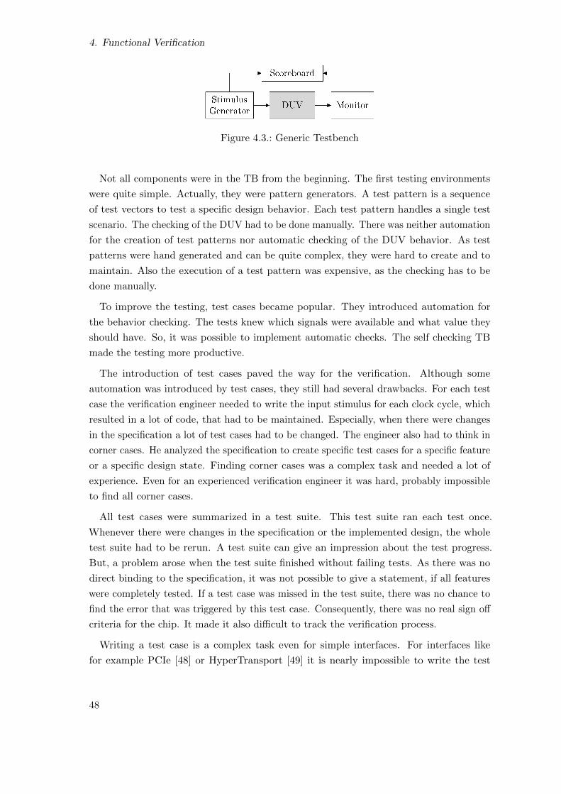
4. Functional Verification
Figure 4.3.: Generic Testbench
Not all components were in the TB from the beginning. The first testing environments
were quite simple. Actually, they were pattern generators. A test pattern is a sequence
of test vectors to test a specific design behavior. Each test pattern handles a single test
scenario. The checking of the DUV had to be done manually. There was neither automation
for the creation of test patterns nor automatic checking of the DUV behavior. As test
patterns were hand generated and can be quite complex, they were hard to create and to
maintain. Also the execution of a test pattern was expensive, as the checking has to be
done manually.
To improve the testing, test cases became popular. They introduced automation for
the behavior checking. The tests knew which signals were available and what value they
should have. So, it was possible to implement automatic checks. The self checking TB
made the testing more productive.
The introduction of test cases paved the way for the verification. Although some
automation was introduced by test cases, they still had several drawbacks. For each test
case the verification engineer needed to write the input stimulus for each clock cycle, which
resulted in a lot of code, that had to be maintained. Especially, when there were changes
in the specification a lot of test cases had to be changed. The engineer also had to think in
corner cases. He analyzed the specification to create specific test cases for a specific feature
or a specific design state. Finding corner cases was a complex task and needed a lot of
experience. Even for an experienced verification engineer it was hard, probably impossible
to find all corner cases.
All test cases were summarized in a test suite. This test suite ran each test once.
Whenever there were changes in the specification or the implemented design, the whole
test suite had to be rerun. A test suite can give an impression about the test progress.
But, a problem arose when the test suite finished without failing tests. As there was no
direct binding to the specification, it was not possible to give a statement, if all features
were completely tested. If a test case was missed in the test suite, there was no chance to
find the error that was triggered by this test case. Consequently, there was no real sign off
criteria for the chip. It made it also difficult to track the verification process.
Writing a test case is a complex task even for simple interfaces. For interfaces like
for example PCIe [48] or HyperTransport [49] it is nearly impossible to write the test
48

4.1. Verification Methodology
patterns for the initialization, credit management, and retransmission for each test case
from scratch. Therefore, people came up with Bus Functional Models (BFMs). A BFM is
a test component which encapsulates the functionality of a single interface and provides
the user with different high level functions for accessing the interface. Typical functions
include read and write accesses to the interface. BFMs reduced the test case complexity,
but still it was a complex task to write a reasonable test case. Additionally, there was no
standard for building BFMs. Each BFM had its own programming interface and its own
way for configuration. This made it hard to integrate it into a TB.
Due to the fact that the design complexity grew, the conclusion could be drawn, that
more features needed to be tested, as well as the complexity of test case also increased.
For many chip designs there are large building blocks, which are reused from one
generation to another. This includes building blocks for common interfaces like PCIe, but
also building blocks for on chip networks or Functional Units (FUs). It would require to
rewrite the test code for every design when using simple test cases.
To overcome all the issues with test cases, people came up with the verification. The goal
of verification is to ensure that all features of a design work as intended in the specification.
There are several methodologies and technique available to improve verification efficiency.
This includes a more efficient generation of stimulus, an improved checking of the DUV
behavior and a better way to track progress of the verification effort. A modern verification
methodology also has a strong support for reusing verification Intellectual Property (IP)
in different verification projects. The following sections describe the available verification
methodologies and techniques. Thereafter, a complete verification methodology is described
a for a complex hardware design.
4.1. Verification Methodology
The common simulation based testing of a hardware design reaches its limits with current
SOCs. They are too complex to finish the testing within a reasonable amount of time. So,
new verification techniques and verification technologies are used in the industry to close
this gap. This section gives an overview of the methods and methodologies used in a state
of the art verification project.
4.1.1. Verification Techniques
There are different verification techniques available, which are shown in figure 4.4 on the
following page. A verification technique is a method used to verify a hardware design.
Although there are different techniques available, they are normally used together for
49
4. Functional Verification
Figure 4.4.: Verification Techniques
an efficient verification process. Each technique is suitable for a special aspect of the
verification.
4.1.1.1. Transaction Based Verification
Writing a TB for a large hardware design is a challenging task. Because of the complexity,
a lot of verification code has to be written. The test developer must write every single test
vector, which tends to be time consuming. To simplify the test code, but also the code for
checking the DUV behavior, people came up with the Transaction Based Verification (TBV)
as depicted in figure 4.5 on the next page. The TBV adds an abstraction layer to the TB.
This follows from the observation, that each interaction of the TB with the DUV is a closed
operation or can be split into several closed operations. Examples for such operations are
a read or a write to/from the DUV. These basic operations are called transactions. A
transaction includes all attributes needed like command type, or the attached data needed
to fulfill the operation. As a transaction is an abstract object, it can not be sent directly
to the DUV. It has no information about the interface protocol to the DUV. Therefore, a
special component called driver, that is part of the stimulus generator, is used in the TBV.
The driver sends the transactions to the DUV interface and transforms the transaction into
interface signals. Interface control signals like a valid can be omitted in the transaction, as
the driver generates them itself according to the interface specification. Once the driver
is implemented, the test writer only has to deal with transactions. He does not need to
know every detail of the interface signals. Also complex interface behavior like the credit
management for a flow control mechanism is completely hidden from the test writer.
The checking of the black box behavior of the DUV is also done by using transactions.
The driver forwards the transactions sent to the SCB. The response of the DUV is collected
by a component called monitor. The monitor samples the interface signals of the DUV
and creates a transaction out of them. The collected transaction is then sent to the SCB.
The SCB compares the received response transaction with the request transaction sent
before. Due to the use of transactions inside the SCB and thereby a higher abstraction
level of the DUV behavior, the complexity required to model the DUV behavior can be
significantly reduced.
50
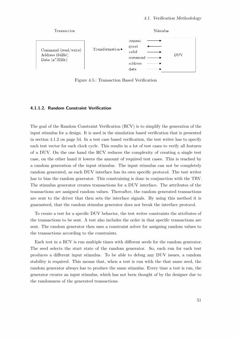
4.1. Verification Methodology
Figure 4.5.: Transaction Based Verification
4.1.1.2. Random Constraint Verification
The goal of the Random Constraint Verification (RCV) is to simplify the generation of the
input stimulus for a design. It is used in the simulation based verification that is presented
in section 4.1.2 on page 54. In a test case based verification, the test writer has to specify
each test vector for each clock cycle. This results in a lot of test cases to verify all features
of a DUV. On the one hand the RCV reduces the complexity of creating a single test
case, on the other hand it lowers the amount of required test cases. This is reached by
a random generation of the input stimulus. The input stimulus can not be completely
random generated, as each DUV interface has its own specific protocol. The test writer
has to bias the random generator. This constraining is done in conjunction with the TBV.
The stimulus generator creates transactions for a DUV interface. The attributes of the
transactions are assigned random values. Thereafter, the random generated transactions
are sent to the driver that then sets the interface signals. By using this method it is
guaranteed, that the random stimulus generator does not break the interface protocol.
To create a test for a specific DUV behavior, the test writer constraints the attributes of
the transactions to be sent. A test also includes the order in that specific transactions are
sent. The random generator then uses a constraint solver for assigning random values to
the transactions according to the constraints.
Each test in a RCV is run multiple times with different seeds for the random generator.
The seed selects the start state of the random generator. So, each run for each test
produces a different input stimulus. To be able to debug any DUV issues, a random
stability is required. This means that, when a test is run with the that same seed, the
random generator always has to produce the same stimulus. Every time a test is run, the
generator creates an input stimulus, which has not been thought of by the designer due to
the randomness of the generated transactions.
51
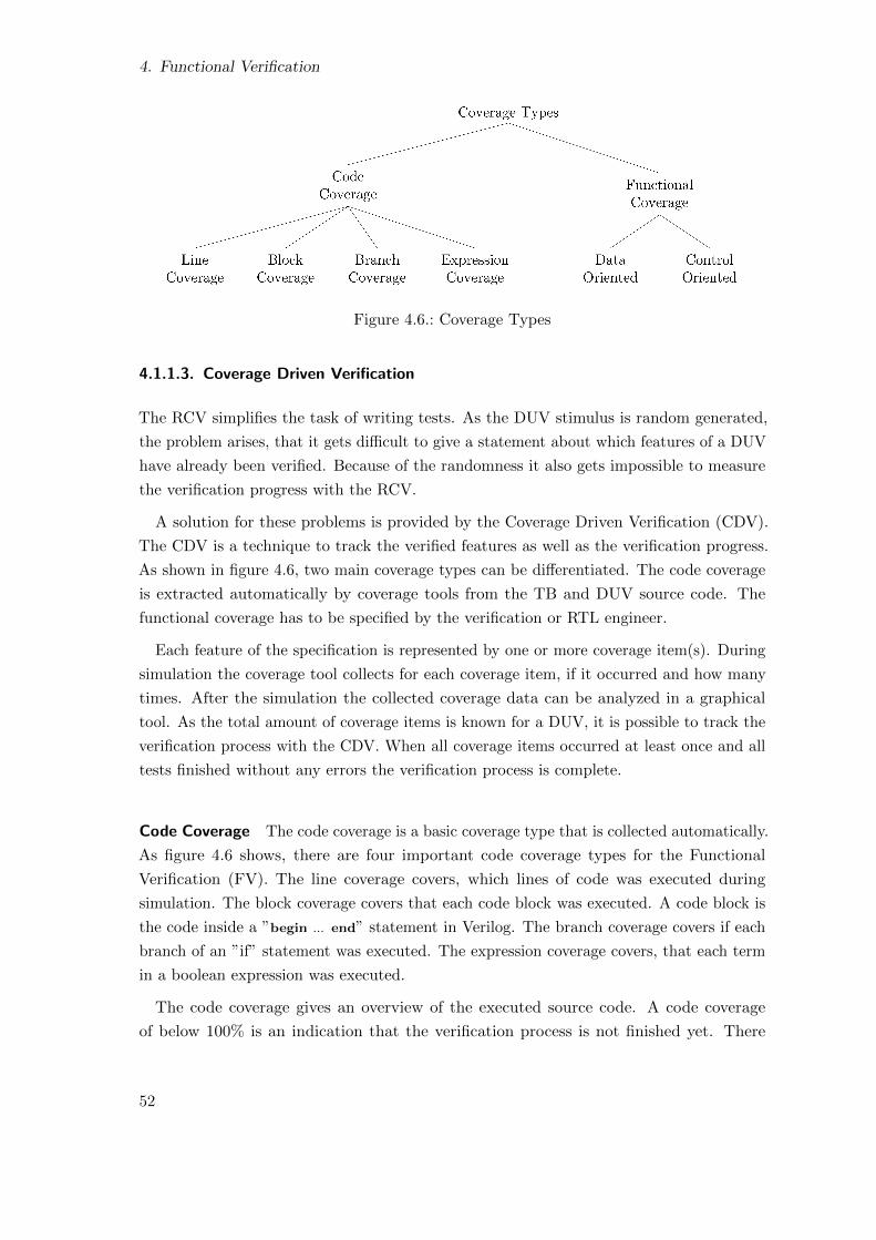
4. Functional Verification
Figure 4.6.: Coverage Types
4.1.1.3. Coverage Driven Verification
The RCV simplifies the task of writing tests. As the DUV stimulus is random generated,
the problem arises, that it gets difficult to give a statement about which features of a DUV
have already been verified. Because of the randomness it also gets impossible to measure
the verification progress with the RCV.
A solution for these problems is provided by the Coverage Driven Verification (CDV).
The CDV is a technique to track the verified features as well as the verification progress.
As shown in figure 4.6, two main coverage types can be differentiated. The code coverage
is extracted automatically by coverage tools from the TB and DUV source code. The
functional coverage has to be specified by the verification or RTL engineer.
Each feature of the specification is represented by one or more coverage item(s). During
simulation the coverage tool collects for each coverage item, if it occurred and how many
times. After the simulation the collected coverage data can be analyzed in a graphical
tool. As the total amount of coverage items is known for a DUV, it is possible to track the
verification process with the CDV. When all coverage items occurred at least once and all
tests finished without any errors the verification process is complete.
Code Coverage The code coverage is a basic coverage type that is collected automatically.
As figure 4.6 shows, there are four important code coverage types for the Functional
Verification (FV). The line coverage covers, which lines of code was executed during
simulation. The block coverage covers that each code block was executed. A code block is
the code inside a ”begin ... end” statement in Verilog. The branch coverage covers if each
branch of an ”if” statement was executed. The expression coverage covers, that each term
in a boolean expression was executed.
The code coverage gives an overview of the executed source code. A code coverage
of below 100% is an indication that the verification process is not finished yet. There
52
4.1. Verification Methodology
are two possibilities two improve the code coverage: The code not executed cannot be
executed, because there exists no condition that leads to an execution. This dead code can
be removed. The other possibility is that RCV has not produced the input stimulus to
reach the code. Then either the existing tests must be run more often, or the verification
engineer has to write new tests or modify the existing constraints to reach a full code
coverage.
A code coverage of 100% isn’t a valid sign off criteria. Most complex features of a DUV
cannot be covered by the code coverage. For example, the code coverage is able to cover
that a variable gets assigned. It cannot cover which values were assigned.
Functional Coverage The functional coverage makes it possible to cover DUV behaviors
that cannot be covered by the code coverage. It cannot be generated automatically. The
verification engineer has to specify the functional coverage by himself. The functional
coverage is extracted either from the specification or from the DUV source code to cover
implementation specific behavior.
There are two types of functional coverage: the data oriented and control oriented
coverage. The data oriented coverage covers the values of a given variable that were
assigned. To describe relationships between two or more variables a cross product can
be defined. This cross product describes that all different combinations of the involved
variables have occurred in simulation.
The data oriented coverage covers the DUV state at a given point in time. The control
oriented coverage is able to cover behaviors that span over more than one point in time.
This way, it gets possible to cover for example that if there is a request, a grant is given
later on and at which point in time. The control oriented coverage can be described by
properties, that are also used to describe assertions.
4.1.1.4. Assertion Based Verification
A verification environment needs an automatic checking of the DUV behavior. Assertions
are the common mechanism for this checking. An assertion is a claim about a design
behavior. It is a boolean expression that has to evaluate to true. Otherwise an error is
reported.
There are two basic types of assertions. Safety and liveness assertions. Safety assertions
are defined by a boolean expression. The expression must be true for all times. Safety
assertions have been used for software development for a long time. In a hardware context,
checks are not only needed for a given point in time, but also for different consecutive
points in time.
53
4. Functional Verification
That’s why liveness assertions nowadays are used as well. For liveness assertions boolean
expressions are extended to include a temporal component. For example, this enables to
write a temporal check for a request grant scheme, where the grant is given one or more
clock cycles after the request.
Assertions are described by properties. A property does a claim about a signal behavior.
This property can be used in different contexts. It can be used as an assertion to check
a behavior. Another use case is to use the property as a coverage item. It is marked as
covered, each time the behavior described by the property is seen in the simulation.
Assertions can be used in the formal and the simulation based verification. In the formal
verification assertions describe the legal input of a DUV. For internal signals and outputs
assertions describe what the formal verification tool has to verify. In the simulation based
verification assertions are used as checks and are evaluated in parallel to the simulation.
For an introduction to SystemVerilog Assertion (SVA) refer to chapter A on page 145.
4.1.2. Simulation Based Verification
The Simulation Based Verification (SVB) evolved from the classic test case based hardware
verification approach. It uses a simulator to execute an implemented RTL model. This
model is also called DUV. The SVB extends the test case approach with random constraint
stimulus generation(section 4.1.1.2 on page 51), transaction based verification(section 4.1.1.1
on page 50), and coverage collection(section 4.1.1.3 on page 52). Figure 4.7 shows a typical
SVB environment. It consists of the DUV, the stimulus generators, drivers, monitors, and
a SCB.
For the simulation the input for the DUV must be provided. Therefore, the stimulus
generators create random transactions. The created transactions are controlled by a test,
that constraints the generated transactions. In a typical SVB environment there are several
different tests available to verify different features of the DUV more easily. Following the
TBV a driver is used to generate the input signals for the DUV out of the transactions
from the stimulus generator. One monitor for each output interface of the DUV is used
to sample the DUV responses, and creates a transaction for each received response. The
stimulus generator as well as several monitors forward the collected transactions to the
SCB.
Common DUVs do have more than one input interface. In this case several stimulus
generators are used, one for each interface. Complex test scenarios need to coordinate
the traffic sent on each interface. For example when there are dependencies for the input
stimulus on different interfaces. Therefore a central stimulus generator is used which
controls all other stimulus generators.
54

4.1. Verification Methodology
The SCB is the central component for comparing the received DUV responses with
the expected ones. In the simplest form, the transactions pass the DUV without any
modifications. Then the SCB compares the received with the send transactions. When the
DUV modifies the input transaction or generates new ones, the scoreboard needs to know
more about the functionality of the DUV. An example for new generated transactions is a
DMA operation. There a descriptor, which describes the DMA operation, is sent to the
DMA controller. The controller then generates reads to receive the data from the origin
memory location followed by a several write operations to the target memory location.
The DUV functionality is provided by a reference model to the SCB. The reference model
is a second implementation of the DUV and is derived from the specification. Unlike the
DUV, the reference model does not need to be cycle accurate. It is only used for checking
the DUV’s black box behavior. This simplification makes the development of the reference
model much faster and helps avoiding faults in the reference model. As the reference
model must be developed only by the help of the specification and not by the RTL team,
it represents a second, independent version of the DUV. This redundant representation of
the hardware design minimizes the chance of misinterpreting the specification or missing
features of the hardware design.
The SCB passes the received transactions from the stimulus generators to the reference
model. The reference model then computes the expected DUV responses. As the reference
model is not cycle accurate, it is much faster in generating the response than the DUV.
For this reason, the SCB stores the expected response calculated by the reference model in
several queues. One queue for each output interface of the DUV. When the SCB receives a
response from an interface monitor, this response is compared with the computed response
of the reference model from the corresponding queue. If the response matches the expected
one, it is removed from the response queue. Otherwise an error message is issued by the
SCB and the simulation is aborted. The verification and the RTL engineer then have to
analyze and fix the error, as the error can be in both, the verification or the RTL source
code.
With the RCV the problem arises that it is impossible to track the verified DUV features
and the verification process. Therefore, the SVB is used in conjunction with the CDV.
The CDV tracks the verifications process with the help of coverage items. A verification
methodology, which is based on the SVB and uses the RCV, TBV, and CDV is also called
Metric Driven Verification (MDV) [50].
4.1.3. Formal Verification
The goal of the formal verification is to mathematically prove that an RTL design corre-
sponds to the specification. In contrast to the SVB, the formal verification does not need
55
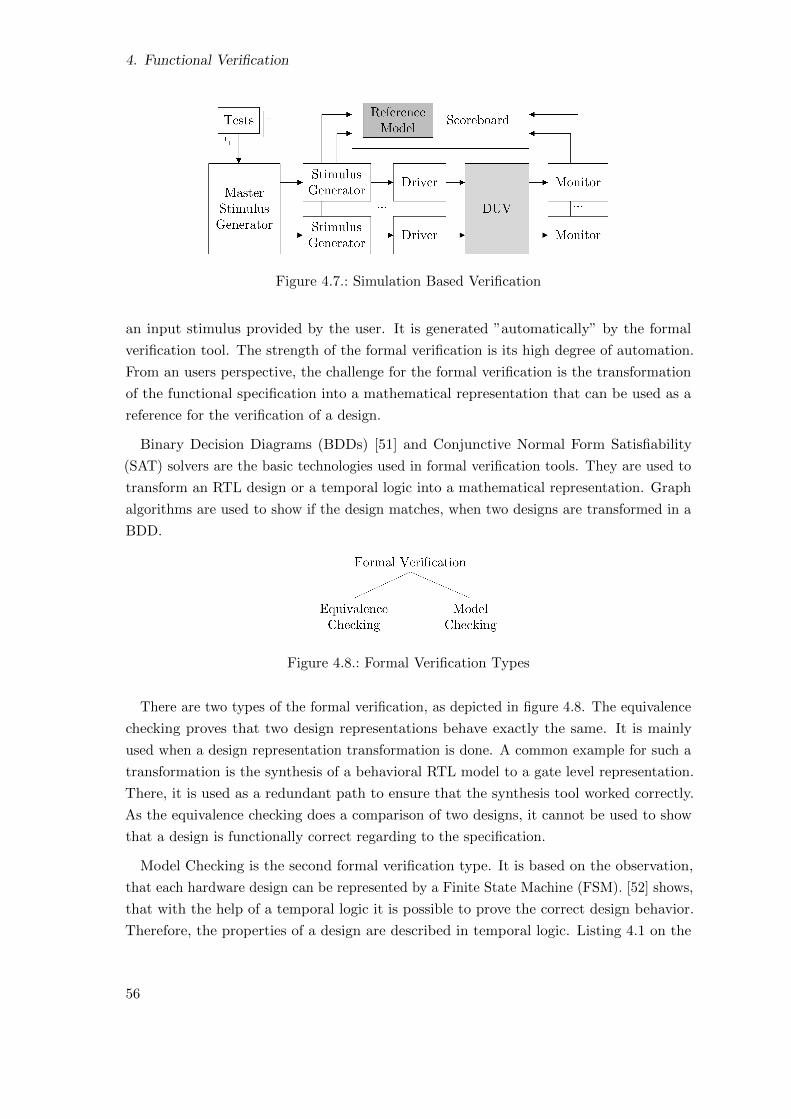
4. Functional Verification
Figure 4.7.: Simulation Based Verification
an input stimulus provided by the user. It is generated ”automatically” by the formal
verification tool. The strength of the formal verification is its high degree of automation.
From an users perspective, the challenge for the formal verification is the transformation
of the functional specification into a mathematical representation that can be used as a
reference for the verification of a design.
Binary Decision Diagrams (BDDs) [51] and Conjunctive Normal Form Satisfiability
(SAT) solvers are the basic technologies used in formal verification tools. They are used to
transform an RTL design or a temporal logic into a mathematical representation. Graph
algorithms are used to show if the design matches, when two designs are transformed in a
BDD.
Figure 4.8.: Formal Verification Types
There are two types of the formal verification, as depicted in figure 4.8. The equivalence
checking proves that two design representations behave exactly the same. It is mainly
used when a design representation transformation is done. A common example for such a
transformation is the synthesis of a behavioral RTL model to a gate level representation.
There, it is used as a redundant path to ensure that the synthesis tool worked correctly.
As the equivalence checking does a comparison of two designs, it cannot be used to show
that a design is functionally correct regarding to the specification.
Model Checking is the second formal verification type. It is based on the observation,
that each hardware design can be represented by a Finite State Machine (FSM). [52] shows,
that with the help of a temporal logic it is possible to prove the correct design behavior.
Therefore, the properties of a design are described in temporal logic. Listing 4.1 on the
56
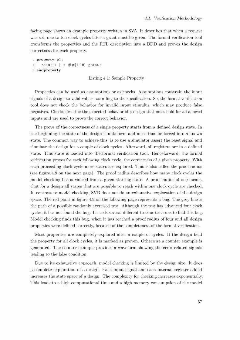
4.1. Verification Methodology
facing page shows an example property written in SVA. It describes that when a request
was set, one to ten clock cycles later a grant must be given. The formal verification tool
transforms the properties and the RTL description into a BDD and proves the design
correctness for each property.
1 property p1 ;
2 r eque s t |−> ##[1:10] grant ;
3 endproperty
Listing 4.1: Sample Property
Properties can be used as assumptions or as checks. Assumptions constrain the input
signals of a design to valid values according to the specification. So, the formal verification
tool does not check the behavior for invalid input stimulus, which may produce false
negatives. Checks describe the expected behavior of a design that must hold for all allowed
inputs and are used to prove the correct behavior.
The prove of the correctness of a single property starts from a defined design state. In
the beginning the state of the design is unknown, and must thus be forced into a known
state. The common way to achieve this, is to use a simulator assert the reset signal and
simulate the design for a couple of clock cycles. Afterward, all registers are in a defined
state. This state is loaded into the formal verification tool. Henceforward, the formal
verification proves for each following clock cycle, the correctness of a given property. With
each proceeding clock cycle more states are explored. This is also called the proof radius
(see figure 4.9 on the next page). The proof radius describes how many clock cycles the
model checking has advanced from a given starting state. A proof radius of one means,
that for a design all states that are possible to reach within one clock cycle are checked.
In contrast to model checking, SVB does not do an exhaustive exploration of the design
space. The red point in figure 4.9 on the following page represents a bug. The grey line is
the path of a possible randomly exercised test. Although the test has advanced four clock
cycles, it has not found the bug. It needs several different tests or test runs to find this bug.
Model checking finds this bug, when it has reached a proof radius of four and all design
properties were defined correctly, because of the completeness of the formal verification.
Most properties are completely explored after a couple of cycles. If the design held
the property for all clock cycles, it is marked as proven. Otherwise a counter example is
generated. The counter example provides a waveform showing the error related signals
leading to the false condition.
Due to its exhaustive approach, model checking is limited by the design size. It does
a complete exploration of a design. Each input signal and each internal register added
increases the state space of a design. The complexity for checking increases exponentially.
This leads to a high computational time and a high memory consumption of the model
57
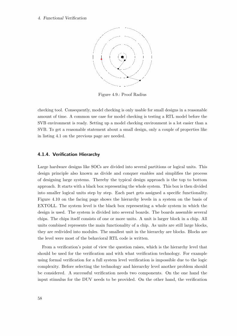
4. Functional Verification
Figure 4.9.: Proof Radius
checking tool. Consequently, model checking is only usable for small designs in a reasonable
amount of time. A common use case for model checking is testing a RTL model before the
SVB environment is ready. Setting up a model checking environment is a lot easier than a
SVB. To get a reasonable statement about a small design, only a couple of properties like
in listing 4.1 on the previous page are needed.
4.1.4. Verification Hierarchy
Large hardware designs like SOCs are divided into several partitions or logical units. This
design principle also known as divide and conquer enables and simplifies the process
of designing large systems. Thereby the typical design approach is the top to bottom
approach. It starts with a black box representing the whole system. This box is then divided
into smaller logical units step by step. Each part gets assigned a specific functionality.
Figure 4.10 on the facing page shows the hierarchy levels in a system on the basis of
EXTOLL. The system level is the black box representing a whole system in which the
design is used. The system is divided into several boards. The boards assemble several
chips. The chips itself consists of one or more units. A unit is larger block in a chip. All
units combined represents the main functionality of a chip. As units are still large blocks,
they are redivided into modules. The smallest unit in the hierarchy are blocks. Blocks are
the level were most of the behavioral RTL code is written.
From a verification’s point of view the question raises, which is the hierarchy level that
should be used for the verification and with what verification technology. For example
using formal verification for a full system level verification is impossible due to the logic
complexity. Before selecting the technology and hierarchy level another problem should
be considered. A successful verification needs two components. On the one hand the
input stimulus for the DUV needs to be provided. On the other hand, the verification
58
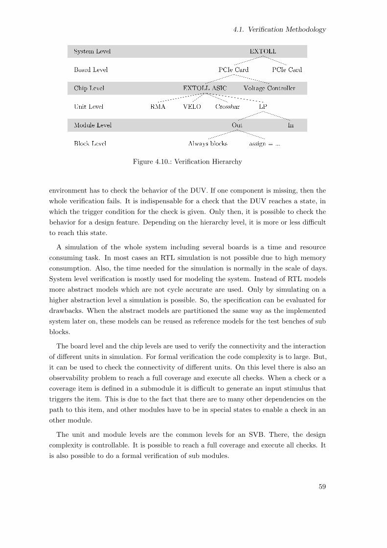
4.1. Verification Methodology
Figure 4.10.: Verification Hierarchy
environment has to check the behavior of the DUV. If one component is missing, then the
whole verification fails. It is indispensable for a check that the DUV reaches a state, in
which the trigger condition for the check is given. Only then, it is possible to check the
behavior for a design feature. Depending on the hierarchy level, it is more or less difficult
to reach this state.
A simulation of the whole system including several boards is a time and resource
consuming task. In most cases an RTL simulation is not possible due to high memory
consumption. Also, the time needed for the simulation is normally in the scale of days.
System level verification is mostly used for modeling the system. Instead of RTL models
more abstract models which are not cycle accurate are used. Only by simulating on a
higher abstraction level a simulation is possible. So, the specification can be evaluated for
drawbacks. When the abstract models are partitioned the same way as the implemented
system later on, these models can be reused as reference models for the test benches of sub
blocks.
The board level and the chip levels are used to verify the connectivity and the interaction
of different units in simulation. For formal verification the code complexity is to large. But,
it can be used to check the connectivity of different units. On this level there is also an
observability problem to reach a full coverage and execute all checks. When a check or a
coverage item is defined in a submodule it is difficult to generate an input stimulus that
triggers the item. This is due to the fact that there are to many other dependencies on the
path to this item, and other modules have to be in special states to enable a check in an
other module.
The unit and module levels are the common levels for an SVB. There, the design
complexity is controllable. It is possible to reach a full coverage and execute all checks. It
is also possible to do a formal verification of sub modules.
59

4. Functional Verification
For the block level an SVB is not applicable. The complexity of the TB exceeds the
complexity of the code to be verified. On this level formal verification is popular for the
verification. It enables the RTL designer to check his code before the SVB environment for
larger modules are ready.
4.1.5. Verification Planning
The verification of a large system is a complex task. A system has different features that
must be verified to ensure that the system works in all operational conditions as intended.
Although, there are features that are considered more important than others, all features
need to verified. As there are many features in a large system, it gets hard to keep track of
all features and to have a predictable verification process. To fill this gap verification plans
are used. They are the single instance to keep track of all verification related information.
As such, the items of the verification plan define the metric for the verification progress.
Figure 4.11 on the next page depicts the general structure of such a verification plan.
Before the verification starts, a specification of the system and its parts is created. Those
specifications are used to create the verification plan. But, these specifications are not the
single source of the verification plan. Other sources include information from the RTL
designers for implementation specific coverage and checks, and knowledge of the verification
engineer about the verification process.
The most important part of the verification plan is the features of the design section. It
is extracted from the specification and describes each single feature of the design. Checks
and coverage items are derived from these features, which need to be included in the
verification environment.
The verification plan summarizes all required resources. This includes the required tools
and licenses, as they must be available during the complete verification. A missing tool
or license can delay the whole verification effort by weeks. Resources also includes the
manpower required for the project.
Another important and mandatory part of the verification plan are test scenarios. Each
test scenario describes the input stimulus for the SVB for a single test. The test scenarios
are grouped by the different TBs which are available for the verification project.
An advantage of verification over testing is the predictability of the verification process
when it is finished. Therefore, criteria need to defined when the verification can be finished
or stopped. These completion criteria are specified in the verification plan. Important
completion criteria are coverage goals, and that all tests and all properties of the formal
verification have successfully passed. The coverage goal for the functional coverage should
be 100%, which means that all features were verified in a verification environment. However,
60
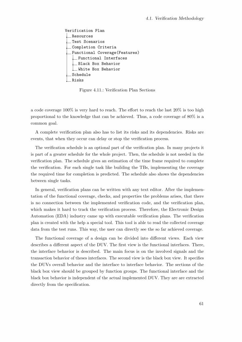
4.1. Verification Methodology
Verification Plan
Resources
Test Scenarios
Completion Criteria
Functional Coverage(Features)
Functional Interfaces
Black Box Behavior
White Box Behavior
Schedule
Risks
Figure 4.11.: Verification Plan Sections
a code coverage 100% is very hard to reach. The effort to reach the last 20% is too high
proportional to the knowledge that can be achieved. Thus, a code coverage of 80% is a
common goal.
A complete verification plan also has to list its risks and its dependencies. Risks are
events, that when they occur can delay or stop the verification process.
The verification schedule is an optional part of the verification plan. In many projects it
is part of a greater schedule for the whole project. Then, the schedule is not needed in the
verification plan. The schedule gives an estimation of the time frame required to complete
the verification. For each single task like building the TBs, implementing the coverage
the required time for completion is predicted. The schedule also shows the dependencies
between single tasks.
In general, verification plans can be written with any text editor. After the implemen-
tation of the functional coverage, checks, and properties the problems arises, that there
is no connection between the implemented verification code, and the verification plan,
which makes it hard to track the verification process. Therefore, the Electronic Design
Automation (EDA) industry came up with executable verification plans. The verification
plan is created with the help a special tool. This tool is able to read the collected coverage
data from the test runs. This way, the user can directly see the so far achieved coverage.
The functional coverage of a design can be divided into different views. Each view
describes a different aspect of the DUV. The first view is the functional interfaces. There,
the interface behavior is described. The main focus is on the involved signals and the
transaction behavior of theses interfaces. The second view is the black box view. It specifies
the DUVs overall behavior and the interface to interface behavior. The sections of the
black box view should be grouped by function groups. The functional interface and the
black box behavior is independent of the actual implemented DUV. They are are extracted
directly from the specification.
61
4. Functional Verification
To be able to define implementation specific functional coverage the white box view is
used. It opens the black box and describes the internal DUV behavior. The white box
coverage has to be defined by the RTL designer in cooperation with a verification engineer.
As it is difficult the specify the coverage for RTL code when its implementation is finished,
it is a good design practice to define the coverage and checks as early as possible. This
has the benefit, that when a module is implemented checks are already there, which then
can be used in a first formal verification run. For defining the white box coverage inside
the verification plan the following steps should be taken. With this approach no signal
behavior is missed, because it recommends to analyze each signal.
1. Add the unit hierarchy as sections in the verification plan
2. Add a comment for each module describing its function
3. Add the coverage points and checks for each sub module
• Start with the interface signals of the module
• Which is the expected interaction with other signals inside the module? →define a check
• What are important interactions between signals? → define a coverage item
• Continue with internal signals and output signals
4.1.6. Verification Cycle
Figure 4.12 on the facing page gives an overview of the complete verification cycle. A
complete specification for the chip/system is needed, before the verification starts. Once
the specification is finished the RTL team starts with the implementation of the design. In
parallel the verification team starts the verification process. First, a verification plan as
described in section 4.1.5 on page 60 is created. The verification plan specifies which units
are verified in a SVB environment and which with formal verification. Secondly, the TBs
for the units are created. The TBs are build with a methodology like Universal Verification
Methodology (UVM) (see section 4.1.7 on page 64). The simulation is started for the first
time, when the TB’s code is finished and the DUV is ready. In this phase many bugs are
found in both the RTL and verification code. That’s why, a close cooperation between
the verification and the RTL engineer is needed for fixing the bugs. The regressions are
started, as soon as the simulation of single tests does not fail any more.
A regression is the process of running tests for a TBs multiple times with different seeds.
Each seed sets a different start state for the constraint solver and therefore a different
stimulus for each test run is created. When a test in a regression fails, the failure has to be
analyzed and fixed by the responsible verification and RTL engineers for the corresponding
62
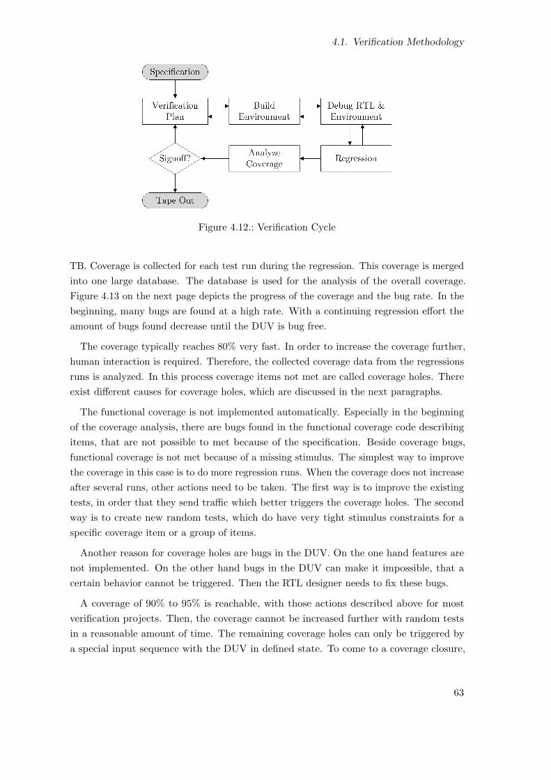
4.1. Verification Methodology
Figure 4.12.: Verification Cycle
TB. Coverage is collected for each test run during the regression. This coverage is merged
into one large database. The database is used for the analysis of the overall coverage.
Figure 4.13 on the next page depicts the progress of the coverage and the bug rate. In the
beginning, many bugs are found at a high rate. With a continuing regression effort the
amount of bugs found decrease until the DUV is bug free.
The coverage typically reaches 80% very fast. In order to increase the coverage further,
human interaction is required. Therefore, the collected coverage data from the regressions
runs is analyzed. In this process coverage items not met are called coverage holes. There
exist different causes for coverage holes, which are discussed in the next paragraphs.
The functional coverage is not implemented automatically. Especially in the beginning
of the coverage analysis, there are bugs found in the functional coverage code describing
items, that are not possible to met because of the specification. Beside coverage bugs,
functional coverage is not met because of a missing stimulus. The simplest way to improve
the coverage in this case is to do more regression runs. When the coverage does not increase
after several runs, other actions need to be taken. The first way is to improve the existing
tests, in order that they send traffic which better triggers the coverage holes. The second
way is to create new random tests, which do have very tight stimulus constraints for a
specific coverage item or a group of items.
Another reason for coverage holes are bugs in the DUV. On the one hand features are
not implemented. On the other hand bugs in the DUV can make it impossible, that a
certain behavior cannot be triggered. Then the RTL designer needs to fix these bugs.
A coverage of 90% to 95% is reachable, with those actions described above for most
verification projects. Then, the coverage cannot be increased further with random tests
in a reasonable amount of time. The remaining coverage holes can only be triggered by
a special input sequence with the DUV in defined state. To come to a coverage closure,
63
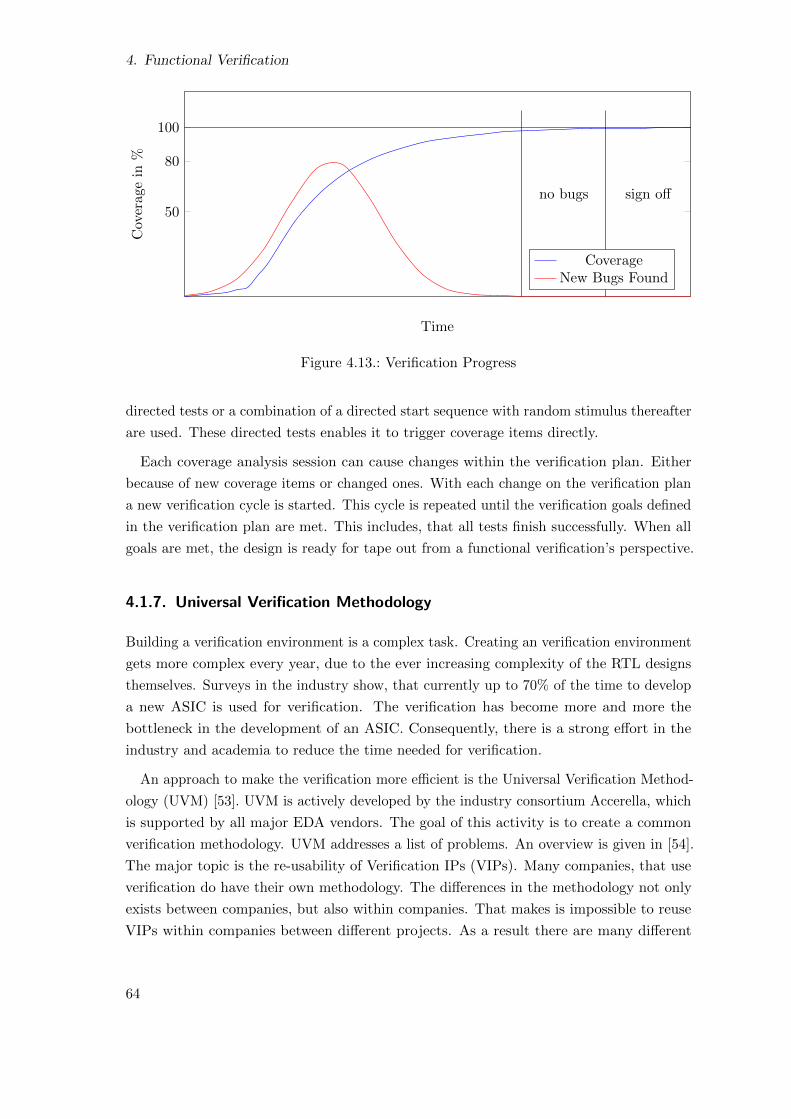
4. Functional Verification
50
80
100
sign offno bugs
Time
Cov
erag
ein
%
CoverageNew Bugs Found
Figure 4.13.: Verification Progress
directed tests or a combination of a directed start sequence with random stimulus thereafter
are used. These directed tests enables it to trigger coverage items directly.
Each coverage analysis session can cause changes within the verification plan. Either
because of new coverage items or changed ones. With each change on the verification plan
a new verification cycle is started. This cycle is repeated until the verification goals defined
in the verification plan are met. This includes, that all tests finish successfully. When all
goals are met, the design is ready for tape out from a functional verification’s perspective.
4.1.7. Universal Verification Methodology
Building a verification environment is a complex task. Creating an verification environment
gets more complex every year, due to the ever increasing complexity of the RTL designs
themselves. Surveys in the industry show, that currently up to 70% of the time to develop
a new ASIC is used for verification. The verification has become more and more the
bottleneck in the development of an ASIC. Consequently, there is a strong effort in the
industry and academia to reduce the time needed for verification.
An approach to make the verification more efficient is the Universal Verification Method-
ology (UVM) [53]. UVM is actively developed by the industry consortium Accerella, which
is supported by all major EDA vendors. The goal of this activity is to create a common
verification methodology. UVM addresses a list of problems. An overview is given in [54].
The major topic is the re-usability of Verification IPs (VIPs). Many companies, that use
verification do have their own methodology. The differences in the methodology not only
exists between companies, but also within companies. That makes is impossible to reuse
VIPs within companies between different projects. As a result there are many different
64
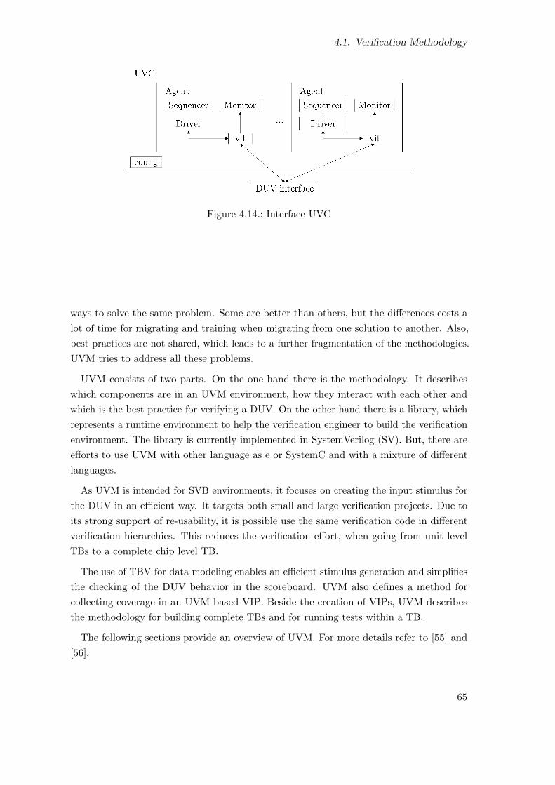
4.1. Verification Methodology
Figure 4.14.: Interface UVC
ways to solve the same problem. Some are better than others, but the differences costs a
lot of time for migrating and training when migrating from one solution to another. Also,
best practices are not shared, which leads to a further fragmentation of the methodologies.
UVM tries to address all these problems.
UVM consists of two parts. On the one hand there is the methodology. It describes
which components are in an UVM environment, how they interact with each other and
which is the best practice for verifying a DUV. On the other hand there is a library, which
represents a runtime environment to help the verification engineer to build the verification
environment. The library is currently implemented in SystemVerilog (SV). But, there are
efforts to use UVM with other language as e or SystemC and with a mixture of different
languages.
As UVM is intended for SVB environments, it focuses on creating the input stimulus for
the DUV in an efficient way. It targets both small and large verification projects. Due to
its strong support of re-usability, it is possible use the same verification code in different
verification hierarchies. This reduces the verification effort, when going from unit level
TBs to a complete chip level TB.
The use of TBV for data modeling enables an efficient stimulus generation and simplifies
the checking of the DUV behavior in the scoreboard. UVM also defines a method for
collecting coverage in an UVM based VIP. Beside the creation of VIPs, UVM describes
the methodology for building complete TBs and for running tests within a TB.
The following sections provide an overview of UVM. For more details refer to [55] and
[56].
65
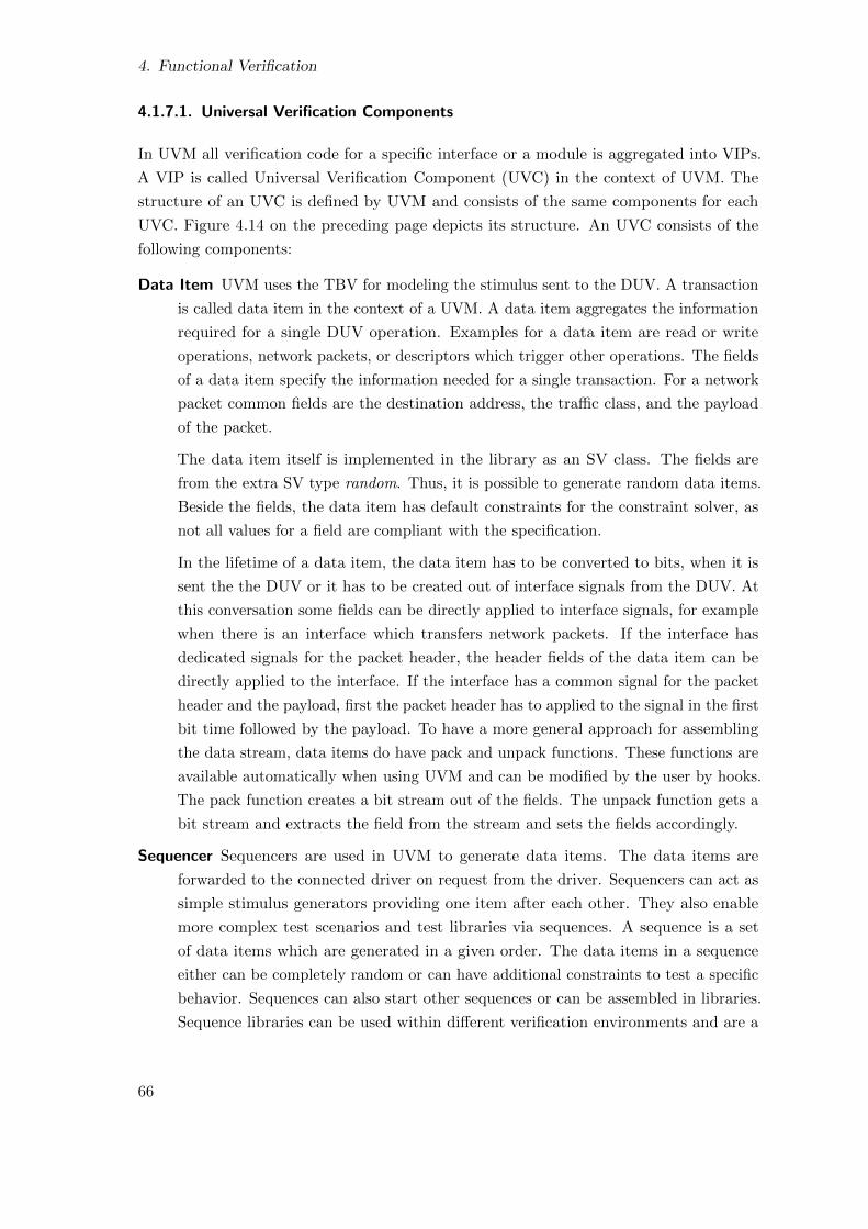
4. Functional Verification
4.1.7.1. Universal Verification Components
In UVM all verification code for a specific interface or a module is aggregated into VIPs.
A VIP is called Universal Verification Component (UVC) in the context of UVM. The
structure of an UVC is defined by UVM and consists of the same components for each
UVC. Figure 4.14 on the preceding page depicts its structure. An UVC consists of the
following components:
Data Item UVM uses the TBV for modeling the stimulus sent to the DUV. A transaction
is called data item in the context of a UVM. A data item aggregates the information
required for a single DUV operation. Examples for a data item are read or write
operations, network packets, or descriptors which trigger other operations. The fields
of a data item specify the information needed for a single transaction. For a network
packet common fields are the destination address, the traffic class, and the payload
of the packet.
The data item itself is implemented in the library as an SV class. The fields are
from the extra SV type random. Thus, it is possible to generate random data items.
Beside the fields, the data item has default constraints for the constraint solver, as
not all values for a field are compliant with the specification.
In the lifetime of a data item, the data item has to be converted to bits, when it is
sent the the DUV or it has to be created out of interface signals from the DUV. At
this conversation some fields can be directly applied to interface signals, for example
when there is an interface which transfers network packets. If the interface has
dedicated signals for the packet header, the header fields of the data item can be
directly applied to the interface. If the interface has a common signal for the packet
header and the payload, first the packet header has to applied to the signal in the first
bit time followed by the payload. To have a more general approach for assembling
the data stream, data items do have pack and unpack functions. These functions are
available automatically when using UVM and can be modified by the user by hooks.
The pack function creates a bit stream out of the fields. The unpack function gets a
bit stream and extracts the field from the stream and sets the fields accordingly.
Sequencer Sequencers are used in UVM to generate data items. The data items are
forwarded to the connected driver on request from the driver. Sequencers can act as
simple stimulus generators providing one item after each other. They also enable
more complex test scenarios and test libraries via sequences. A sequence is a set
of data items which are generated in a given order. The data items in a sequence
either can be completely random or can have additional constraints to test a specific
behavior. Sequences can also start other sequences or can be assembled in libraries.
Sequence libraries can be used within different verification environments and are a
66

4.1. Verification Methodology
key feature for the re-usability of UVM.
A sequencer controls one driver and therefore a single DUV interface. For complex test
scenarios it is necessary to control the stimulus on more than one DUV interface. For
that reason, UVM defines virtual sequencers. Virtual sequencers are not connected
to a driver. Instead, they are connected two one or more other sequencers. Via these
connections, virtual sequencers can issue data items or sequences on other sequencers.
Sequencers can also be reactive. Reactive sequencers receive a request from the DUV
and provide corresponding responses. Reactive sequencers can be both non virtual
or virtual.
Driver The driver in UVM handles the signals on a DUV interface. It requests data items
from the connected sequencer. The data item is then converted into interface signals
according to the specification.
Monitor The monitor samples the signals on an interface and creates a data item for each
transaction seen. The monitor also checks the signal behavior of the interface, and
the fields of the collected data item. The field check verifies, that each field only has
allowed values. For example, when a data item has field that indicates the length of
the attached data, a check can ensure that length field and actual data length are
the same.
Coverage collection for the interface is also done in the monitor.
Agent The agent is used as a container for the driver, sequencer and monitor. It represents
a single instance on an interface. If there is a bus, there can be more than one
instances using the bus. Each single instance is represented by an agent. A single
UVC for a bus interface can have multiple agents. The agent count is adjustable by
the UVC configuration.
A point to point interface has two actors: the sender and the receiver. An UVC for
such an interface does have two agents. A master and a slave agents representing the
sender and the receiver. So, the UVC is able to act as each member of the interface.
An agent can exist in an active or passive mode. An active agent has the driver, the
sequencer and the monitor activated. It can send input stimulus to a DUV. In a
passive agent only the monitor is activated. The driver and the sequencer are disabled.
It is used to monitor and check an interface. The modes are used in different ways.
In an UVC for a point to point interface only the master agent or the slave agent
has to generate the stimulus for a DUV. Then the not needed agent is set to passive,
and thereby disabled. This functionality also improves the re-usability of an UVC.
When the UVC is used to verify a module of a bigger design, its agents are active to
generate the input stimulus. Is the module integrated into a bigger TB, then the
67
4. Functional Verification
Figure 4.15.: Module UVC
interface which was driven by the UVC before, is driven by a surrounding module.
To still be able to monitor and check the interface, the UVC agents are set to passive
mode. This monitoring improves the overall observability of the complete DUV.
The mode of an agent is configured via the built-in UVM configuration mechanism,
which is described in section 4.1.7.3 on page 71.
UVCs can be distinguished between interface and module UVCs. An interface UVC,
which is shown in figure 4.14 on page 65, is directly connected to a DUV. It handles the
signals of the interface. The agents do have a driver, a sequencer, and a monitor.
A module UVC, as shown in figure 4.15, is used to control other UVCs. It does not have
an interface connection to a DUV. The agents only consists of a monitor and a sequencer
without a driver. Module UVCs are used to partition the TB. For example, in a large
design there are standard interfaces to connect the different modules. For each interface an
interface UVC is created. In a TB for a module these UVCs are used to provide the input
stimulus on the interfaces of the DUV. The data items used on these UVCs are related
to the interface. Protocols on top of the interface, which are used by the module itself,
can be hard to realize with constraints on the data items of the interface UVC. In this
case a module UVC is used to simplify the stimulus generation, but also to increase the
re-usability. If the interface of the module changes to a new interface, only the interface
UVC changes. The module UVC and all tests, checks including the scoreboard stay the
same.
4.1.7.2. UVM Phases
A typical verification environment consists of several independent components like stimulus
generators, monitor, and scoreboards. As they are independent of each other, problems
occur, when a simulation starts or at the end of a simulation. At the simulation start, all
components need to be created. Then, they need to be connected to the DUV and other
components. Not before all components are created and connected, the reset of the DUV
is started. If this order is violated, the TB does not behave as intended. For example
components access other components before they are created. Another problem that arises
68

4.1. Verification Methodology
Figure 4.16.: UVM Phases
is the end of a simulation. In a TB there are many transactions on the fly. Before the
simulation can be stopped, all transactions must be finished. Also the DUV needs a drain
time, so that it can enter an idle state and no other operations are in flight. Therefore, all
components need to be stopped at the same time to avoid false error reporting. This can
be a complex task a large environment with many components and transactions.
UVM uses an approach based on phases to provide a synchronization between the
different states of a TB. The scheduling of the phases is done by UVM. Each component
can implement an own function named as the phase to execute code in this phase. These
functions are called automatically by UVM in the corresponding phase. Due to this
automatism, the TB writer does not have to care about the synchronization. Even large
TBs with many components can be set up easily.
The phases used within UVM are depicted in figure 4.16. Each phase has a specific task
as shown below.
Build The build phase is the first UVM phase executed in a simulation. It is used to create
all static components like UVCs, drivers, and scoreboards in the environment. As all
components are arranged in a hierarchy. They are build top down. First the test is
created, followed by the TB, UVC tops, and then further down the hierarchy.
Connect After the build phase is finished, all components in the verification environment
are available. In the connect phase the components are connected with each other.
For example, the sequencers gets connected to the corresponding drivers. It is safe to
connect components across the UVM hierarchy, as all components were create before.
End of Elaboration In the end of elaboration phase final adjustments to the configurations
69

4. Functional Verification
of the components and the connections between them can be made.
Start of Simulation The start of simulation phase is intended to print banners, the final
topology and configuration of the TB.
Run The run phase is the single simulation time consuming phase in UVM. In this phase
the sequencers create the stimulus. The scoreboard(s) check the responses from the
DUV. When all transactions defined by the test are sent and the DUV is idle again
after processing all input stimulus, the run phase can advance to the next phase.
Extract In the extract phase analysis components retrieve information from the scoreboards
and monitors. This information can be used for statistics.
Check The check phase does an end of test checking with the information received in the
extract phase. A common check is that the scoreboard does not have any outstanding
transactions.
Report In the report phase the final statistics and result of the simulation is displayed.
A problem arises when the run phase advances to the extract phase. The phase change
should only occur, when all components have finished their tasks in the run phase. UVM
therefore uses an objection mechanism. Each component can raise an objection on a phase
object and drops it when its task is finished. The run phase advances to the next phase
not until all objections that were raised before are dropped. An optional drain time can be
specified. This time is waited after the last objection has dropped before UVM advances to
the next phase. If a new objection is raised, the drain time is stopped until all objections
are dropped again. For example, a sequence raises an objection on start up and drops it,
when all its transactions are sent. Thus, it is possible to synchronize the transition to the
next phase with little overhead for the verification engineer even for environments with a
large number of concurrent components.
4.1.7.3. UVM Configuration Mechanism
An advantage of UVM is its design for re-usability. Therefore, it uses UVCs to encapsulate
the behavior of an interface or a module. An UVC is a generic object, which represents the
different modes of an interface. For example there are master and slave agents. Depending
on the environment a UVC is used in, either the master or the slave agent is active.
Consequently, there must be a mechanism for the configuration of the UVCs. It is possible
to directly change the UVC code to change its configuration. But, this approach has several
drawbacks. Not always the UVC is completely available. When the UVC is provided by
third party vendor, its core code is encrypted. Even when the code is available, it can
cause trouble modifying the code directly. When the UVC is used within different TBs
and in each use case a different configuration is needed, the UVC needs to be copied for
70
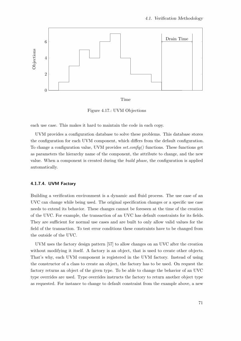
4.1. Verification Methodology
0
2
4
6Drain Time
Time
Ob
ject
ions
Figure 4.17.: UVM Objections
each use case. This makes it hard to maintain the code in each copy.
UVM provides a configuration database to solve these problems. This database stores
the configuration for each UVM component, which differs from the default configuration.
To change a configuration value, UVM provides set config() functions. These functions get
as parameters the hierarchy name of the component, the attribute to change, and the new
value. When a component is created during the build phase, the configuration is applied
automatically.
4.1.7.4. UVM Factory
Building a verification environment is a dynamic and fluid process. The use case of an
UVC can change while being used. The original specification changes or a specific use case
needs to extend its behavior. These changes cannot be foreseen at the time of the creation
of the UVC. For example, the transaction of an UVC has default constraints for its fields.
They are sufficient for normal use cases and are built to only allow valid values for the
field of the transaction. To test error conditions these constraints have to be changed from
the outside of the UVC.
UVM uses the factory design pattern [57] to allow changes on an UVC after the creation
without modifying it itself. A factory is an object, that is used to create other objects.
That’s why, each UVM component is registered in the UVM factory. Instead of using
the constructor of a class to create an object, the factory has to be used. On request the
factory returns an object of the given type. To be able to change the behavior of an UVC
type overrides are used. Type overrides instructs the factory to return another object type
as requested. For instance to change to default constraint from the example above, a new
71
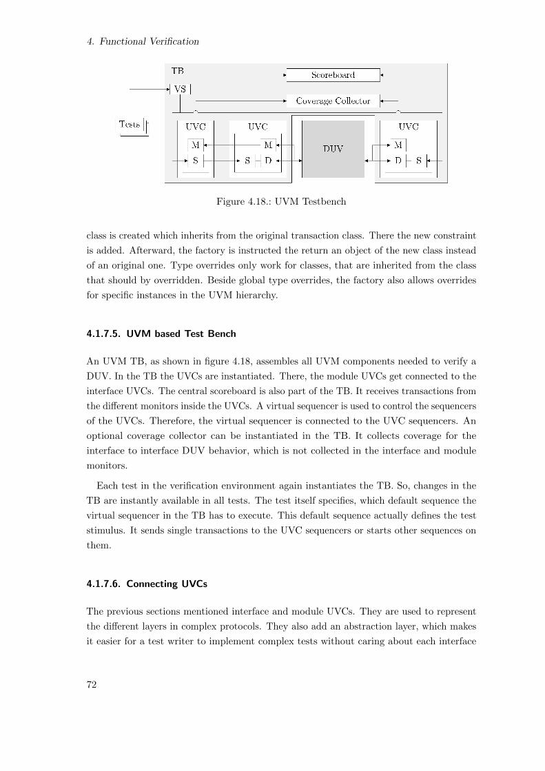
4. Functional Verification
Figure 4.18.: UVM Testbench
class is created which inherits from the original transaction class. There the new constraint
is added. Afterward, the factory is instructed the return an object of the new class instead
of an original one. Type overrides only work for classes, that are inherited from the class
that should by overridden. Beside global type overrides, the factory also allows overrides
for specific instances in the UVM hierarchy.
4.1.7.5. UVM based Test Bench
An UVM TB, as shown in figure 4.18, assembles all UVM components needed to verify a
DUV. In the TB the UVCs are instantiated. There, the module UVCs get connected to the
interface UVCs. The central scoreboard is also part of the TB. It receives transactions from
the different monitors inside the UVCs. A virtual sequencer is used to control the sequencers
of the UVCs. Therefore, the virtual sequencer is connected to the UVC sequencers. An
optional coverage collector can be instantiated in the TB. It collects coverage for the
interface to interface DUV behavior, which is not collected in the interface and module
monitors.
Each test in the verification environment again instantiates the TB. So, changes in the
TB are instantly available in all tests. The test itself specifies, which default sequence the
virtual sequencer in the TB has to execute. This default sequence actually defines the test
stimulus. It sends single transactions to the UVC sequencers or starts other sequences on
them.
4.1.7.6. Connecting UVCs
The previous sections mentioned interface and module UVCs. They are used to represent
the different layers in complex protocols. They also add an abstraction layer, which makes
it easier for a test writer to implement complex tests without caring about each interface
72
4.1. Verification Methodology
detail and enables the strong re-usability of UVM.
This sections describes a way how to establish the connection between UVCs. Therefore,
it shows how the different UVM facilities can be used together to build a verification
environment.
As depicted in figure 4.19 on the following page, the layering of UVCs consists of two
parts. First, the data items created in the module UVC must be forwarded to the sequencer
in the interface UVC. Henceforward, the data items of the module UVC are called upper
items and the data items of the interface UVC are called lower items. The sequencer of the
interface UVC has to transform the upper items into lower items, before the lower items
can be sent to the driver. Second, the lower items collected by the interface monitor need
to be transformed into upper level items, in order that the monitor in the module UVC
can forward the upper item.
In an interface UVC, the sequencer and the driver communicate via Transaction Layer
Modeling (TLM) [58]. TLM is a standard for transaction based modeling. Particularly,
TLM defines channels for the communication between transaction based components. UVM
uses these channels for the transportation of data items between components. Therefore,
each sequencer has a default sequence item export. Each driver has a sequence item pull
port. These ports are connected in the agent they are used in. Afterward, the driver can
request new data items from the sequencer by using the get() function of its pull port.
As each sequencer has a sequence item export, this port can be used also to send data
items from the module sequencer to the interface sequencer. This has the advantage, that
the sequences for the module sequencer stays the same, regardless which interface UVC
is used. A standard sequencer has no sequence item pull port. Consequently, a sequence
item pull port has to be added to the interface sequencer. It is not advisable to change the
sequencer in the interface UVC. A sequence item pull port is always parameterized with a
data item type. An interface sequencer parameterized with an external data item type
has a reduced re-usability, because of its dependency to the upper data item. Instead, a
factory override should be used. Therefore, a new sequencer which extends the interface
sequencer is created. In this sequencer a sequence item pull port is added. Thereafter, a
factory instance override is added, which instructs the factory to return the new sequencer
instead of the interface sequence, when the sequencer is created in the interface UVC. In
the TB the port of module sequencer can be connected to the port of the new sequencer.
With the new sequencer the upper items are forwarded to the interface sequencer. To sent
the items to the driver, they have to be converted into lower items. This conversion is done
by a special sequence, which is executed in the interface sequencer. The sequence requests
a new item from the module sequencer via the newly added TLM channel. Depending on
the module and the interface protocol, the conversion creates one or more lower items out
73
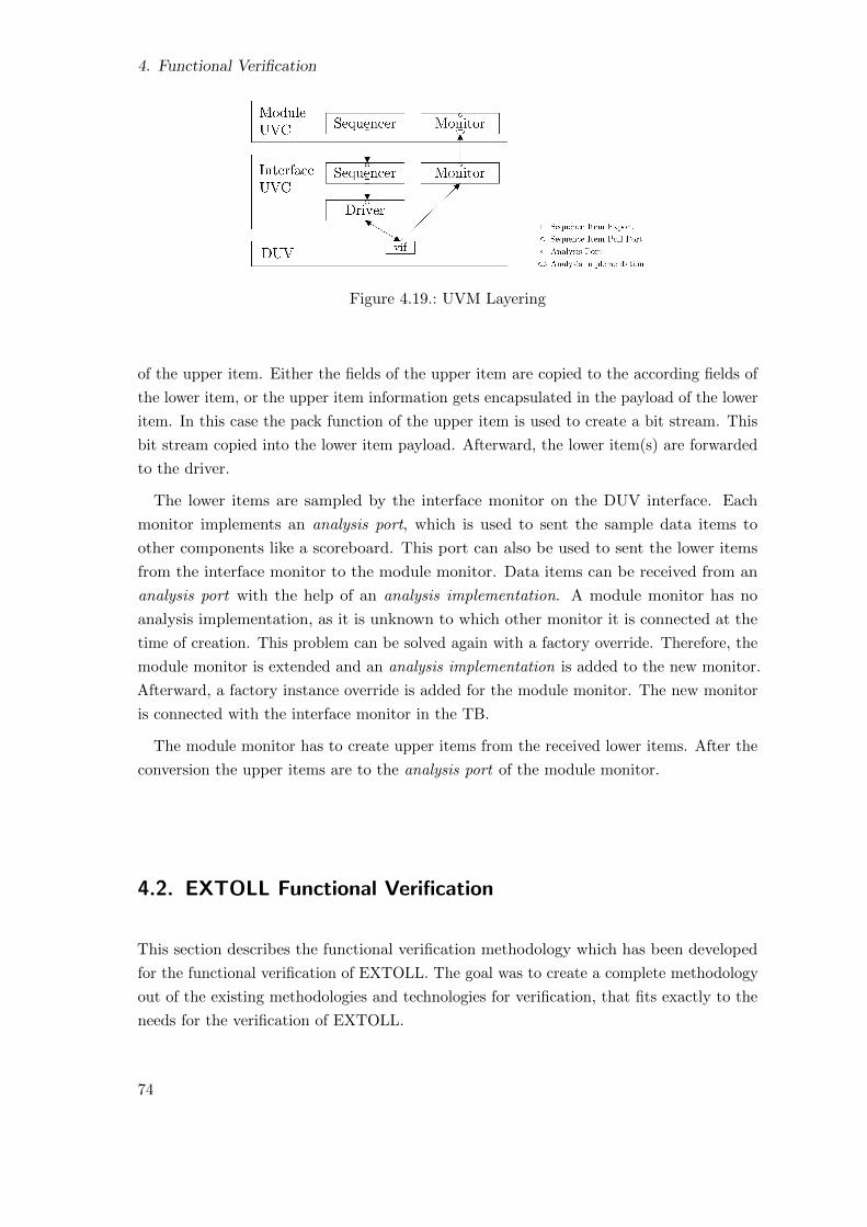
4. Functional Verification
Figure 4.19.: UVM Layering
of the upper item. Either the fields of the upper item are copied to the according fields of
the lower item, or the upper item information gets encapsulated in the payload of the lower
item. In this case the pack function of the upper item is used to create a bit stream. This
bit stream copied into the lower item payload. Afterward, the lower item(s) are forwarded
to the driver.
The lower items are sampled by the interface monitor on the DUV interface. Each
monitor implements an analysis port, which is used to sent the sample data items to
other components like a scoreboard. This port can also be used to sent the lower items
from the interface monitor to the module monitor. Data items can be received from an
analysis port with the help of an analysis implementation. A module monitor has no
analysis implementation, as it is unknown to which other monitor it is connected at the
time of creation. This problem can be solved again with a factory override. Therefore, the
module monitor is extended and an analysis implementation is added to the new monitor.
Afterward, a factory instance override is added for the module monitor. The new monitor
is connected with the interface monitor in the TB.
The module monitor has to create upper items from the received lower items. After the
conversion the upper items are to the analysis port of the module monitor.
4.2. EXTOLL Functional Verification
This section describes the functional verification methodology which has been developed
for the functional verification of EXTOLL. The goal was to create a complete methodology
out of the existing methodologies and technologies for verification, that fits exactly to the
needs for the verification of EXTOLL.
74
4.2. EXTOLL Functional Verification
4.2.1. Functional Verification Roles
In a large verification project like for EXTOLL, many people are involved. There are
system architects, who specify functional blocks of a chip and their interaction with each
other. There are RTL designers, who implement the chip specified by the system architects
in RTL. There are semi custom design flow specialists, who do a synthesis of the RTL
netlist and create the final Graphic Database System (GDS)II view for the tape out. And
there is the functional verification team. They have to ensure, that the implemented chip
conforms to the specification. The functional verification team can be further distinguished
into several roles depending on the skill set of each member. For the EXTOLL verification
project the following roles have been defined, each one with different responsibilities:
TB Creator The TB creator has a strong knowledge of the whole verification process.
He has to decide how each part of a design is verified. Another responsibility is to
build the verification environments for each part. Therefore, a strong knowledge of
verification methodologies like UVM is needed. He also has to maintain the regression
suite.
Coverage/Assertion Specialist Coverage/assertion specialist implements the coverage and
checks defined in the verification. He has a deep knowledge about coverage and
assertion languages like SVA or Property Specification Language (PSL). He don not
need to have a in depth knowledge about the verification process.
Regression Analyst The regression analyst has to examine the coverage progress in the
regression. During regular analysis sessions, he determines the holes in the coverage
and makes proposals how to close these holes. Therefore, he needs a understanding
of the complete system design.
User The user uses the existing verification environments implemented by the TB creators.
Users are typically RTL designers, who wants to do single test runs with his design
before the regression starts or after changes in their design. He also does reruns of
failed regression test runs for debugging.
4.2.2. EXTOLL Verification Analysis
The functional verification of EXTOLL started with an analysis of the design. Goal of the
analysis was to get to know the design and the functionality of each block. Furthermore, it
was important to understand the interactions of the different blocks with each other. As
shown in section 4.1.5 on page 60, the knowledge gained from the analysis has been used
to create a first version of the verification plan.
As depicted in figure 4.20 on the following page, EXTOLL consists of three main parts:
75
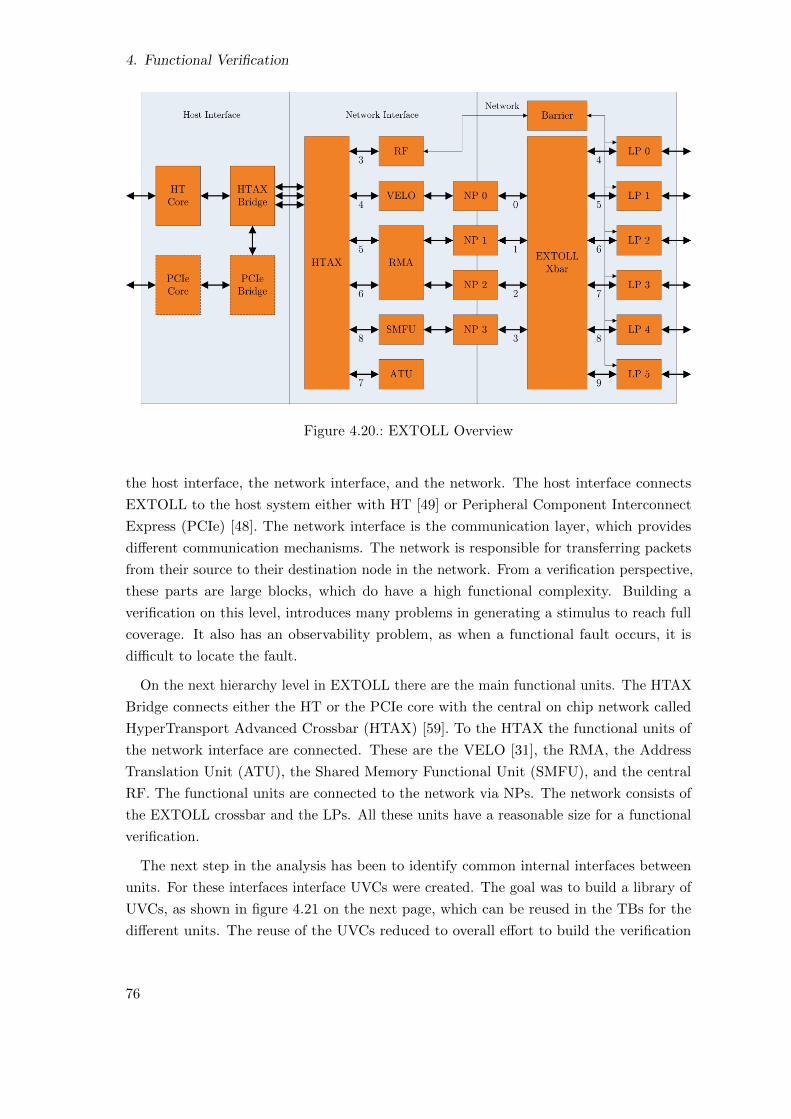
4. Functional Verification
Figure 4.20.: EXTOLL Overview
the host interface, the network interface, and the network. The host interface connects
EXTOLL to the host system either with HT [49] or Peripheral Component Interconnect
Express (PCIe) [48]. The network interface is the communication layer, which provides
different communication mechanisms. The network is responsible for transferring packets
from their source to their destination node in the network. From a verification perspective,
these parts are large blocks, which do have a high functional complexity. Building a
verification on this level, introduces many problems in generating a stimulus to reach full
coverage. It also has an observability problem, as when a functional fault occurs, it is
difficult to locate the fault.
On the next hierarchy level in EXTOLL there are the main functional units. The HTAX
Bridge connects either the HT or the PCIe core with the central on chip network called
HyperTransport Advanced Crossbar (HTAX) [59]. To the HTAX the functional units of
the network interface are connected. These are the VELO [31], the RMA, the Address
Translation Unit (ATU), the Shared Memory Functional Unit (SMFU), and the central
RF. The functional units are connected to the network via NPs. The network consists of
the EXTOLL crossbar and the LPs. All these units have a reasonable size for a functional
verification.
The next step in the analysis has been to identify common internal interfaces between
units. For these interfaces interface UVCs were created. The goal was to build a library of
UVCs, as shown in figure 4.21 on the next page, which can be reused in the TBs for the
different units. The reuse of the UVCs reduced to overall effort to build the verification
76
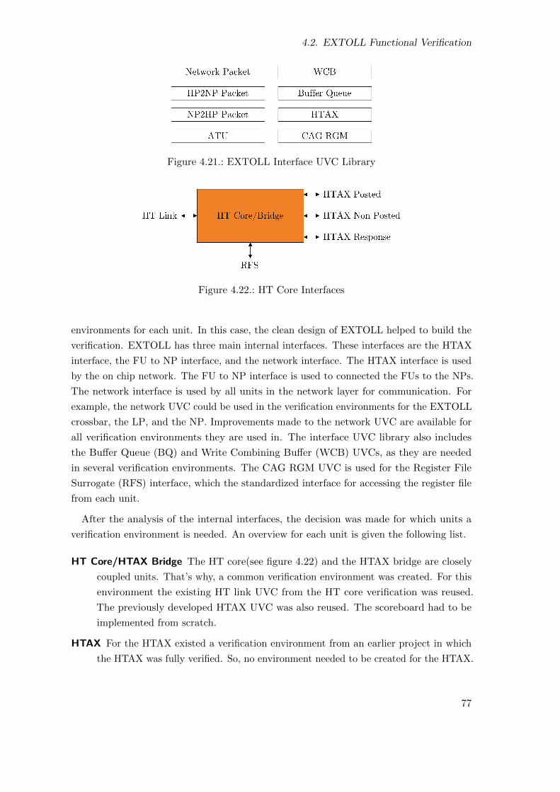
4.2. EXTOLL Functional Verification
Figure 4.21.: EXTOLL Interface UVC Library
Figure 4.22.: HT Core Interfaces
environments for each unit. In this case, the clean design of EXTOLL helped to build the
verification. EXTOLL has three main internal interfaces. These interfaces are the HTAX
interface, the FU to NP interface, and the network interface. The HTAX interface is used
by the on chip network. The FU to NP interface is used to connected the FUs to the NPs.
The network interface is used by all units in the network layer for communication. For
example, the network UVC could be used in the verification environments for the EXTOLL
crossbar, the LP, and the NP. Improvements made to the network UVC are available for
all verification environments they are used in. The interface UVC library also includes
the Buffer Queue (BQ) and Write Combining Buffer (WCB) UVCs, as they are needed
in several verification environments. The CAG RGM UVC is used for the Register File
Surrogate (RFS) interface, which the standardized interface for accessing the register file
from each unit.
After the analysis of the internal interfaces, the decision was made for which units a
verification environment is needed. An overview for each unit is given the following list.
HT Core/HTAX Bridge The HT core(see figure 4.22) and the HTAX bridge are closely
coupled units. That’s why, a common verification environment was created. For this
environment the existing HT link UVC from the HT core verification was reused.
The previously developed HTAX UVC was also reused. The scoreboard had to be
implemented from scratch.
HTAX For the HTAX existed a verification environment from an earlier project in which
the HTAX was fully verified. So, no environment needed to be created for the HTAX.
77
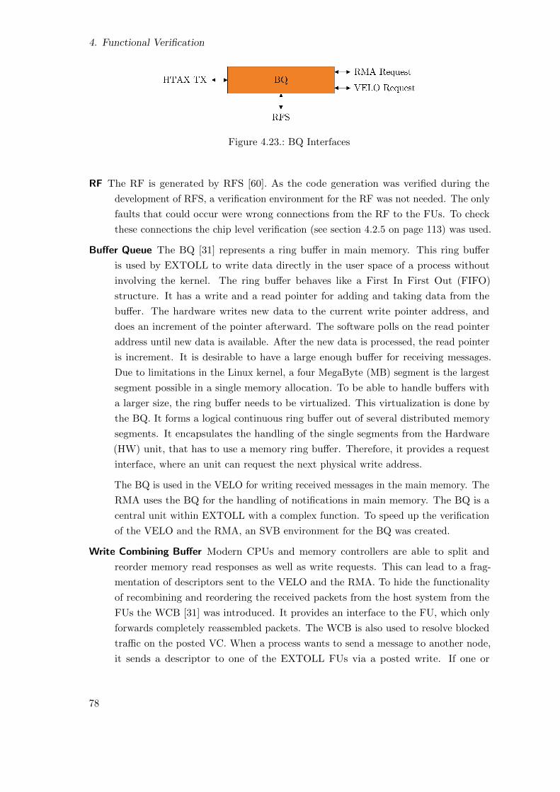
4. Functional Verification
Figure 4.23.: BQ Interfaces
RF The RF is generated by RFS [60]. As the code generation was verified during the
development of RFS, a verification environment for the RF was not needed. The only
faults that could occur were wrong connections from the RF to the FUs. To check
these connections the chip level verification (see section 4.2.5 on page 113) was used.
Buffer Queue The BQ [31] represents a ring buffer in main memory. This ring buffer
is used by EXTOLL to write data directly in the user space of a process without
involving the kernel. The ring buffer behaves like a First In First Out (FIFO)
structure. It has a write and a read pointer for adding and taking data from the
buffer. The hardware writes new data to the current write pointer address, and
does an increment of the pointer afterward. The software polls on the read pointer
address until new data is available. After the new data is processed, the read pointer
is increment. It is desirable to have a large enough buffer for receiving messages.
Due to limitations in the Linux kernel, a four MegaByte (MB) segment is the largest
segment possible in a single memory allocation. To be able to handle buffers with
a larger size, the ring buffer needs to be virtualized. This virtualization is done by
the BQ. It forms a logical continuous ring buffer out of several distributed memory
segments. It encapsulates the handling of the single segments from the Hardware
(HW) unit, that has to use a memory ring buffer. Therefore, it provides a request
interface, where an unit can request the next physical write address.
The BQ is used in the VELO for writing received messages in the main memory. The
RMA uses the BQ for the handling of notifications in main memory. The BQ is a
central unit within EXTOLL with a complex function. To speed up the verification
of the VELO and the RMA, an SVB environment for the BQ was created.
Write Combining Buffer Modern CPUs and memory controllers are able to split and
reorder memory read responses as well as write requests. This can lead to a frag-
mentation of descriptors sent to the VELO and the RMA. To hide the functionality
of recombining and reordering the received packets from the host system from the
FUs the WCB [31] was introduced. It provides an interface to the FU, which only
forwards completely reassembled packets. The WCB is also used to resolve blocked
traffic on the posted VC. When a process wants to send a message to another node,
it sends a descriptor to one of the EXTOLL FUs via a posted write. If one or
78
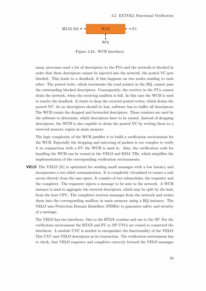
4.2. EXTOLL Functional Verification
Figure 4.24.: WCB Interfaces
many processes send a lot of descriptors to the FUs and the network is blocked in
order that these descriptors cannot be injected into the network, the posted VC gets
blocked. This leads to a deadlock, if this happens on two nodes sending to each
other. The posted write, which increments the read pointer in the BQ, cannot pass
the outstanding blocked descriptors. Consequently, the receiver in the FUs cannot
drain the network, when the receiving mailbox is full. In this case the WCB is used
to resolve the deadlock. It starts to drop the received posted writes, which drains the
posted VC. As no descriptors should be lost, software has to buffer all descriptors.
The WCB counts the dropped and forwarded descriptors. These counters are used by
the software to determine, which descriptors have to be resend. Instead of dropping
descriptors, the WCB is also capable to drain the posted VC by writing them to a
reserved memory region in main memory.
The logic complexity of the WCB justifies it to build a verification environment for
the WCB. Especially the dropping and mirroring of packets is too complex to verify
it in conjunction with a FU the WCB is used in. Also, the verification code for
handling the WCB can be reused in the VELO and RMA TBs, which simplifies the
implementation of the corresponding verification environments.
VELO The VELO [31] is optimized for sending small messages with a low latency and
incorporates a two sided communication. It is completely virtualized to ensure a safe
access directly from the user space. It consists of two submodules, the requester and
the completer. The requester injects a message to be sent in the network. A WCB
instance is used to aggregate the received descriptors, which may be split by the host,
from the host CPU. The completer receives messages from the network and writes
them into the corresponding mailbox in main memory using a BQ instance. The
VELO uses Protection Domain Identifiers (PDIDs) to guarantee safety and security
of a message.
The VELO has two interfaces. One to the HTAX crossbar and one to the NP. For the
verification environment the HTAX and FU to NP UVCs are reused to connected the
interfaces. A module UVC is needed to encapsulate the functionality of the VELO.
This UVC uses VELO descriptors as its transaction. The verification environment has
to check, that VELO requester and completer correctly forward the VELO messages.
79

4. Functional Verification
Figure 4.25.: VELO Interfaces
For the completer it has to be checked that the received messages are written to the
correct mailbox and in the mailbox to the correct segment. The verification has to
focus on the error handling of the VELO, as this a critical point for the chip. It has
to check the VELO behavior for messages received with a wrong PDID and messages
for a disabled mailbox. In both cases the message has to be dropped.
RMA The RMA [61] is used in EXTOLL to realize a remote memory access to other nodes
using DMA. It supports remote put and get operations, as well as locks. As the
VELO, the RMA is fully virtualized. From a software’s perspective, it is possible to
directly access the RMA from the user space without involving the kernel. Because
software operates with virtual addresses and the RMA needs physical address to
perform its operation, an address translation is needed. Therefore, the RMA uses a
functional unit called ATU.
Each RMA operation is specified by a descriptor. The descriptor includes the
operation type and all information needed to fulfill the operation like the memory
addresses for reading and writing data, or the Virtual Process Identifier (VPID).
This descriptor is sent from the host CPU to the RMA, where it is then processed.
The RMA operates directly on the main memory. So, the software is not able to
determine easily, when an operation is finished. To solve this problem, the RMA
supports notifications. These notifications are triggered optionally, when an operation
finishes. Whether a notification is triggered or not is specified in the descriptor. The
notification is written into the mailbox specified by the descriptors VPID. The RMA
uses the BQ for handling theses mailboxes. Like with the VELO, all RMA descriptors
sent over the network are secured with a PDID.
The RMA consists of three major blocks: the requester, the responder, and the
completer. The requester receives descriptors from the host CPU and is the starting
point for all RMA operations. For put operations it first reads the needed data from
main memory. Then, the descriptor is transformed into one or more network descrip-
tors, which are injected into the network. The responder processes get operations
from remote nodes. On a received network descriptor, it reads the data from the
requested main memory address. This data is then sent back to the requesting node.
The completer is the last unit involved in an RMA operation. When it receives an
80

4.2. EXTOLL Functional Verification
Figure 4.26.: RMA Interfaces
network descriptor, it writes the attached data into main memory to the address
specified in the descriptor.
The RMA has the highest functional complexity of all EXTOLL functional units.
Consequently, it is obvious, that a verification environment for this unit is needed. It
has two interfaces to the HTAX, two interfaces which are connected with an NP, an
interface to the BQ, and an interface to the ATU. For all these interfaces, interface
UVCs from the EXTOLL UVC library can be used. A module UVC for the RMA
functionality is also needed. The verification environment has to check, that all
descriptors are processed correctly by the RMA. Error checks include wrong received
PDIDs and descriptors for disabled VPIDs. Also false page translations needs to be
checked. For a complete description of the verification environment for the RMA see
section 4.2.4.1 on page 94.
SMFU EXTOLL introduces a functional unit for non-coherent distributed shared memory
communication called SMFU [33]. Remote memory accesses are handled by forwarding
local load or store transactions to a remote node. This forwarding is completely
done in hardware without involvement of any software layers. So, the SMFU directly
enables shared memory memory paradigms like PGAS in hardware.
The address space gets partitioned into local and global addresses. Local addresses
point directly to the local memory. The local memory has a private and a shared
partition. The shared local partitions of all nodes are mapped into the global address
space. So, each node is able to directly access the shared local memory of all other
nodes.
A CPU can access remote memory by a load or store operation to a global address.
Therefore, the global address space is mapped to the SMFU in a local node. So,
the system automatically forwards the operation to the SMFU. It encapsulates the
received operation which is either a posted write or non-posted read, and sends it via
the network to the remote node. The remote SMFU extracts the operation from the
network packet, which is then send to the host main memory. Responses for reads
81
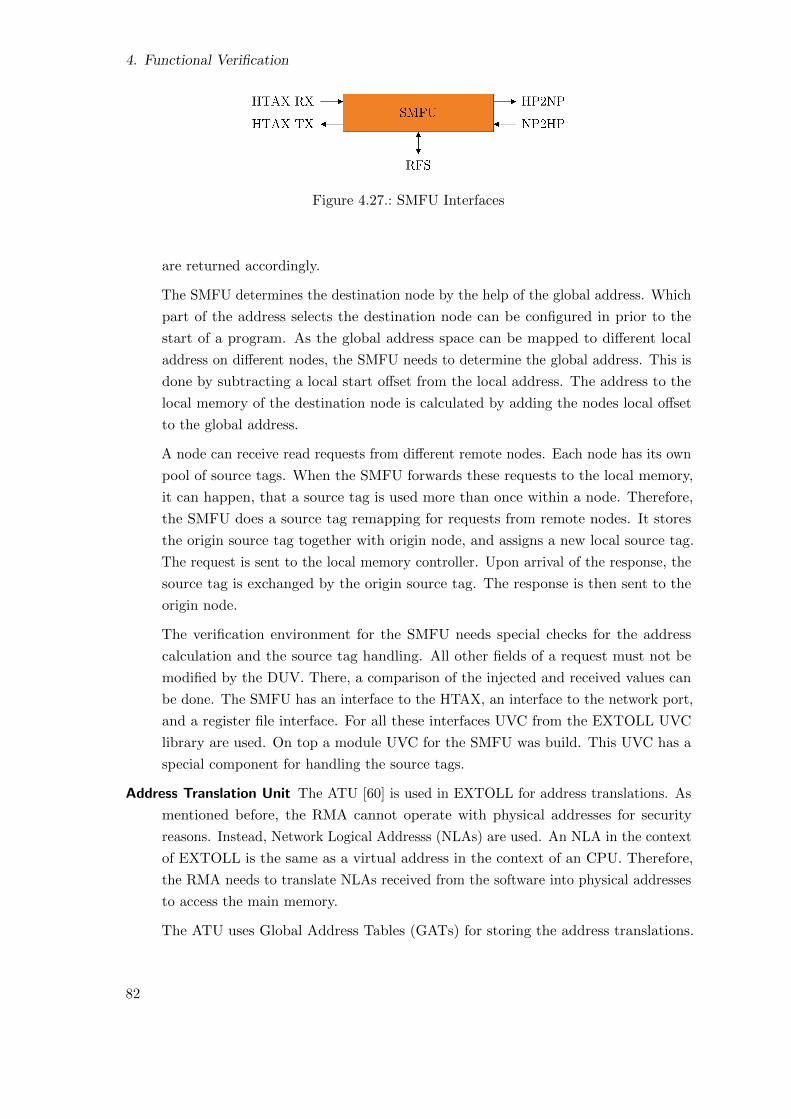
4. Functional Verification
Figure 4.27.: SMFU Interfaces
are returned accordingly.
The SMFU determines the destination node by the help of the global address. Which
part of the address selects the destination node can be configured in prior to the
start of a program. As the global address space can be mapped to different local
address on different nodes, the SMFU needs to determine the global address. This is
done by subtracting a local start offset from the local address. The address to the
local memory of the destination node is calculated by adding the nodes local offset
to the global address.
A node can receive read requests from different remote nodes. Each node has its own
pool of source tags. When the SMFU forwards these requests to the local memory,
it can happen, that a source tag is used more than once within a node. Therefore,
the SMFU does a source tag remapping for requests from remote nodes. It stores
the origin source tag together with origin node, and assigns a new local source tag.
The request is sent to the local memory controller. Upon arrival of the response, the
source tag is exchanged by the origin source tag. The response is then sent to the
origin node.
The verification environment for the SMFU needs special checks for the address
calculation and the source tag handling. All other fields of a request must not be
modified by the DUV. There, a comparison of the injected and received values can
be done. The SMFU has an interface to the HTAX, an interface to the network port,
and a register file interface. For all these interfaces UVC from the EXTOLL UVC
library are used. On top a module UVC for the SMFU was build. This UVC has a
special component for handling the source tags.
Address Translation Unit The ATU [60] is used in EXTOLL for address translations. As
mentioned before, the RMA cannot operate with physical addresses for security
reasons. Instead, Network Logical Addresss (NLAs) are used. An NLA in the context
of EXTOLL is the same as a virtual address in the context of an CPU. Therefore,
the RMA needs to translate NLAs received from the software into physical addresses
to access the main memory.
The ATU uses Global Address Tables (GATs) for storing the address translations.
82
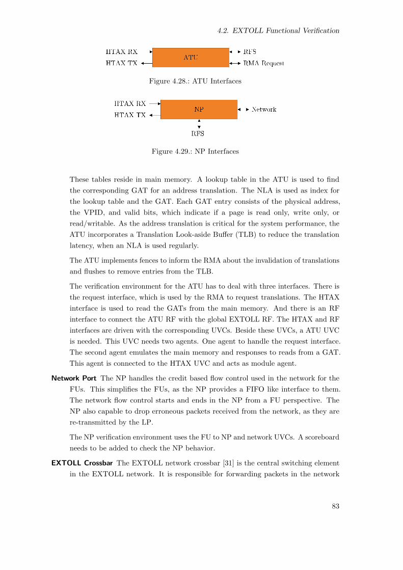
4.2. EXTOLL Functional Verification
Figure 4.28.: ATU Interfaces
Figure 4.29.: NP Interfaces
These tables reside in main memory. A lookup table in the ATU is used to find
the corresponding GAT for an address translation. The NLA is used as index for
the lookup table and the GAT. Each GAT entry consists of the physical address,
the VPID, and valid bits, which indicate if a page is read only, write only, or
read/writable. As the address translation is critical for the system performance, the
ATU incorporates a Translation Look-aside Buffer (TLB) to reduce the translation
latency, when an NLA is used regularly.
The ATU implements fences to inform the RMA about the invalidation of translations
and flushes to remove entries from the TLB.
The verification environment for the ATU has to deal with three interfaces. There is
the request interface, which is used by the RMA to request translations. The HTAX
interface is used to read the GATs from the main memory. And there is an RF
interface to connect the ATU RF with the global EXTOLL RF. The HTAX and RF
interfaces are driven with the corresponding UVCs. Beside these UVCs, a ATU UVC
is needed. This UVC needs two agents. One agent to handle the request interface.
The second agent emulates the main memory and responses to reads from a GAT.
This agent is connected to the HTAX UVC and acts as module agent.
Network Port The NP handles the credit based flow control used in the network for the
FUs. This simplifies the FUs, as the NP provides a FIFO like interface to them.
The network flow control starts and ends in the NP from a FU perspective. The
NP also capable to drop erroneous packets received from the network, as they are
re-transmitted by the LP.
The NP verification environment uses the FU to NP and network UVCs. A scoreboard
needs to be added to check the NP behavior.
EXTOLL Crossbar The EXTOLL network crossbar [31] is the central switching element
in the EXTOLL network. It is responsible for forwarding packets in the network
83
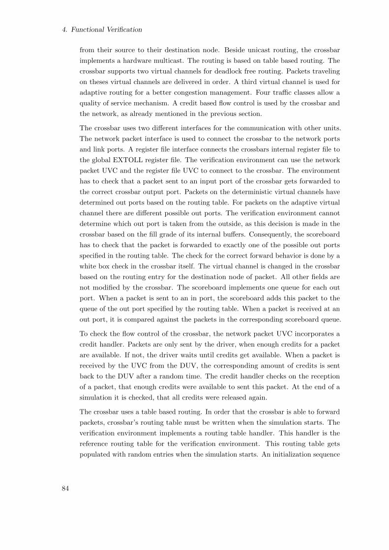
4. Functional Verification
from their source to their destination node. Beside unicast routing, the crossbar
implements a hardware multicast. The routing is based on table based routing. The
crossbar supports two virtual channels for deadlock free routing. Packets traveling
on theses virtual channels are delivered in order. A third virtual channel is used for
adaptive routing for a better congestion management. Four traffic classes allow a
quality of service mechanism. A credit based flow control is used by the crossbar and
the network, as already mentioned in the previous section.
The crossbar uses two different interfaces for the communication with other units.
The network packet interface is used to connect the crossbar to the network ports
and link ports. A register file interface connects the crossbars internal register file to
the global EXTOLL register file. The verification environment can use the network
packet UVC and the register file UVC to connect to the crossbar. The environment
has to check that a packet sent to an input port of the crossbar gets forwarded to
the correct crossbar output port. Packets on the deterministic virtual channels have
determined out ports based on the routing table. For packets on the adaptive virtual
channel there are different possible out ports. The verification environment cannot
determine which out port is taken from the outside, as this decision is made in the
crossbar based on the fill grade of its internal buffers. Consequently, the scoreboard
has to check that the packet is forwarded to exactly one of the possible out ports
specified in the routing table. The check for the correct forward behavior is done by a
white box check in the crossbar itself. The virtual channel is changed in the crossbar
based on the routing entry for the destination node of packet. All other fields are
not modified by the crossbar. The scoreboard implements one queue for each out
port. When a packet is sent to an in port, the scoreboard adds this packet to the
queue of the out port specified by the routing table. When a packet is received at an
out port, it is compared against the packets in the corresponding scoreboard queue.
To check the flow control of the crossbar, the network packet UVC incorporates a
credit handler. Packets are only sent by the driver, when enough credits for a packet
are available. If not, the driver waits until credits get available. When a packet is
received by the UVC from the DUV, the corresponding amount of credits is sent
back to the DUV after a random time. The credit handler checks on the reception
of a packet, that enough credits were available to sent this packet. At the end of a
simulation it is checked, that all credits were released again.
The crossbar uses a table based routing. In order that the crossbar is able to forward
packets, crossbar’s routing table must be written when the simulation starts. The
verification environment implements a routing table handler. This handler is the
reference routing table for the verification environment. This routing table gets
populated with random entries when the simulation starts. An initialization sequence
84
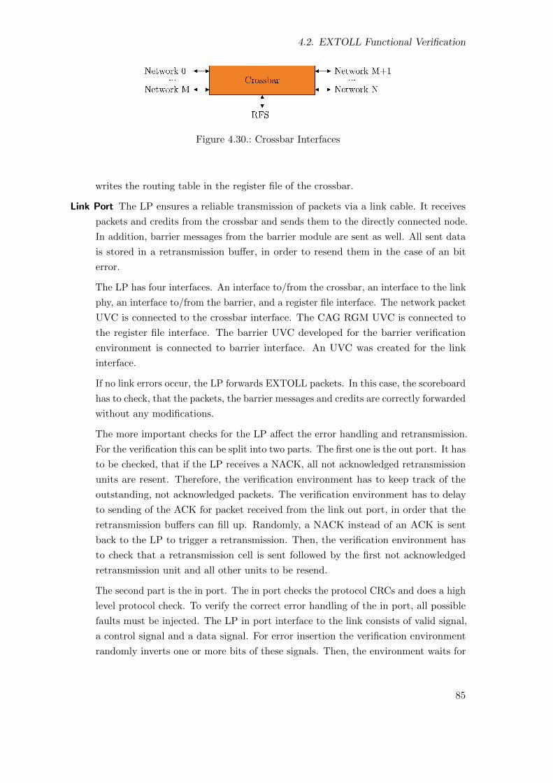
4.2. EXTOLL Functional Verification
Figure 4.30.: Crossbar Interfaces
writes the routing table in the register file of the crossbar.
Link Port The LP ensures a reliable transmission of packets via a link cable. It receives
packets and credits from the crossbar and sends them to the directly connected node.
In addition, barrier messages from the barrier module are sent as well. All sent data
is stored in a retransmission buffer, in order to resend them in the case of an bit
error.
The LP has four interfaces. An interface to/from the crossbar, an interface to the link
phy, an interface to/from the barrier, and a register file interface. The network packet
UVC is connected to the crossbar interface. The CAG RGM UVC is connected to
the register file interface. The barrier UVC developed for the barrier verification
environment is connected to barrier interface. An UVC was created for the link
interface.
If no link errors occur, the LP forwards EXTOLL packets. In this case, the scoreboard
has to check, that the packets, the barrier messages and credits are correctly forwarded
without any modifications.
The more important checks for the LP affect the error handling and retransmission.
For the verification this can be split into two parts. The first one is the out port. It has
to be checked, that if the LP receives a NACK, all not acknowledged retransmission
units are resent. Therefore, the verification environment has to keep track of the
outstanding, not acknowledged packets. The verification environment has to delay
to sending of the ACK for packet received from the link out port, in order that the
retransmission buffers can fill up. Randomly, a NACK instead of an ACK is sent
back to the LP to trigger a retransmission. Then, the verification environment has
to check that a retransmission cell is sent followed by the first not acknowledged
retransmission unit and all other units to be resend.
The second part is the in port. The in port checks the protocol CRCs and does a high
level protocol check. To verify the correct error handling of the in port, all possible
faults must be injected. The LP in port interface to the link consists of valid signal,
a control signal and a data signal. For error insertion the verification environment
randomly inverts one or more bits of these signals. Then, the environment waits for
85
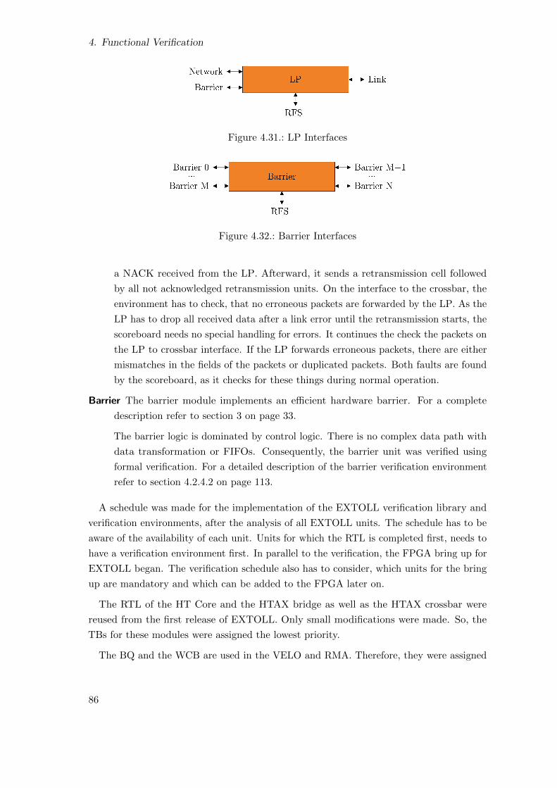
4. Functional Verification
Figure 4.31.: LP Interfaces
Figure 4.32.: Barrier Interfaces
a NACK received from the LP. Afterward, it sends a retransmission cell followed
by all not acknowledged retransmission units. On the interface to the crossbar, the
environment has to check, that no erroneous packets are forwarded by the LP. As the
LP has to drop all received data after a link error until the retransmission starts, the
scoreboard needs no special handling for errors. It continues the check the packets on
the LP to crossbar interface. If the LP forwards erroneous packets, there are either
mismatches in the fields of the packets or duplicated packets. Both faults are found
by the scoreboard, as it checks for these things during normal operation.
Barrier The barrier module implements an efficient hardware barrier. For a complete
description refer to section 3 on page 33.
The barrier logic is dominated by control logic. There is no complex data path with
data transformation or FIFOs. Consequently, the barrier unit was verified using
formal verification. For a detailed description of the barrier verification environment
refer to section 4.2.4.2 on page 113.
A schedule was made for the implementation of the EXTOLL verification library and
verification environments, after the analysis of all EXTOLL units. The schedule has to be
aware of the availability of each unit. Units for which the RTL is completed first, needs to
have a verification environment first. In parallel to the verification, the FPGA bring up for
EXTOLL began. The verification schedule also has to consider, which units for the bring
up are mandatory and which can be added to the FPGA later on.
The RTL of the HT Core and the HTAX bridge as well as the HTAX crossbar were
reused from the first release of EXTOLL. Only small modifications were made. So, the
TBs for these modules were assigned the lowest priority.
The BQ and the WCB are used in the VELO and RMA. Therefore, they were assigned
86
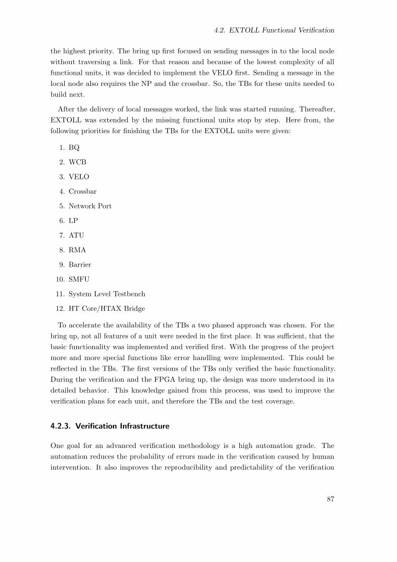
4.2. EXTOLL Functional Verification
the highest priority. The bring up first focused on sending messages in to the local node
without traversing a link. For that reason and because of the lowest complexity of all
functional units, it was decided to implement the VELO first. Sending a message in the
local node also requires the NP and the crossbar. So, the TBs for these units needed to
build next.
After the delivery of local messages worked, the link was started running. Thereafter,
EXTOLL was extended by the missing functional units stop by step. Here from, the
following priorities for finishing the TBs for the EXTOLL units were given:
1. BQ
2. WCB
3. VELO
4. Crossbar
5. Network Port
6. LP
7. ATU
8. RMA
9. Barrier
10. SMFU
11. System Level Testbench
12. HT Core/HTAX Bridge
To accelerate the availability of the TBs a two phased approach was chosen. For the
bring up, not all features of a unit were needed in the first place. It was sufficient, that the
basic functionality was implemented and verified first. With the progress of the project
more and more special functions like error handling were implemented. This could be
reflected in the TBs. The first versions of the TBs only verified the basic functionality.
During the verification and the FPGA bring up, the design was more understood in its
detailed behavior. This knowledge gained from this process, was used to improve the
verification plans for each unit, and therefore the TBs and the test coverage.
4.2.3. Verification Infrastructure
One goal for an advanced verification methodology is a high automation grade. The
automation reduces the probability of errors made in the verification caused by human
intervention. It also improves the reproducibility and predictability of the verification
87
4. Functional Verification
process. To enable this automation a verification infrastructure is needed, which assists all
actors in the verification process.
4.2.3.1. Subversion Directory Structure
During the development of a large ASIC a lot of source code needs to written for the RTL
as well as for the verification. To synchronize the source code between the developers
involved, version control systems are used. Version control systems also enable the tracking
of changes in the source code. For the EXTOLL development Subversion (SVN) was chosen
as version control system, as it is widely adopted and was known to all developers involved.
As there is different code in the SVN repository, a directory structure was developed to
address the following problems:
• Make it easy to locate code in the repository
• Reduce redundant code in the repository
• Allow script automation
• Support different target technologies for EXTOLL
The SVN structure is depicted in figure 4.33 on the next page. The SVN top directory
is separated into two main directories. One for the RTL code named hw/, and for the
verification code named verification/. In the hw/ directory there are subdirectories for the
EXTOLL units called extoll r2/, for the building blocks like FIFOs, and the EXTOLL
targets. Each unit or module has its own subdirectory in the corresponding directory. In
this directory there is its source code, a .f file which lists all source files in this directory.
The .f files are used by the TBs and synthesis tools for a faster read in of the source code.
In the vplan/ directory resides the verification plan for the unit.
EXTOLL can be mapped to different target technologies like FPGAs or ASICs. Each
target can use a different configuration of EXTOLL. For example, as host interface either
HT or PCIe can be used, the internal data path can be 64- or 128-Bit, or the amount of
links can change. Therefore, each target needs a different top level file, a different crossbar,
and a different RF. To reflect these differences, the extoll r2 target/ directory is used. Each
target has an own directory to collect all source files specific to this target.
The verification directory is structured into three subdirectories. The TBs reside in the
tb/ directory. The common/ directory is used for scripts and files used in all TBs. The
UVCs are stored in the UVC/ directory. There, each UVC has its own subdirectory. The
UVC directory structure is defined in [62]. The sv/ subdirectory is used for the SV code,
the doc/ subdirectory for the documentation, and the vpm/ subdirectory for the UVC’s
verification plan.
88
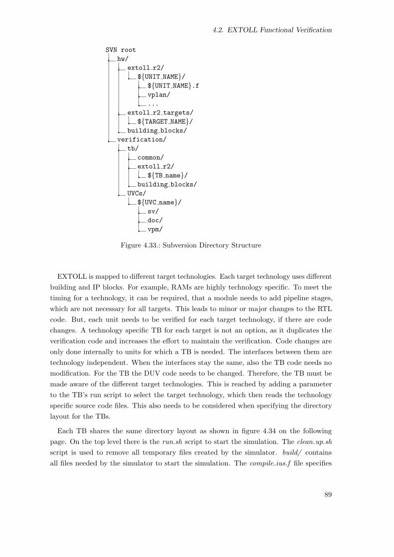
4.2. EXTOLL Functional Verification
SVN root
hw/
extoll r2/
${UNIT NAME}/${UNIT NAME}.fvplan/
...
extoll r2 targets/
${TARGET NAME}/building blocks/
verification/
tb/
common/
extoll r2/
${TB name}/building blocks/
UVCs/
${UVC name}/sv/
doc/
vpm/
Figure 4.33.: Subversion Directory Structure
EXTOLL is mapped to different target technologies. Each target technology uses different
building and IP blocks. For example, RAMs are highly technology specific. To meet the
timing for a technology, it can be required, that a module needs to add pipeline stages,
which are not necessary for all targets. This leads to minor or major changes to the RTL
code. But, each unit needs to be verified for each target technology, if there are code
changes. A technology specific TB for each target is not an option, as it duplicates the
verification code and increases the effort to maintain the verification. Code changes are
only done internally to units for which a TB is needed. The interfaces between them are
technology independent. When the interfaces stay the same, also the TB code needs no
modification. For the TB the DUV code needs to be changed. Therefore, the TB must be
made aware of the different target technologies. This is reached by adding a parameter
to the TB’s run script to select the target technology, which then reads the technology
specific source code files. This also needs to be considered when specifying the directory
layout for the TBs.
Each TB shares the same directory layout as shown in figure 4.34 on the following
page. On the top level there is the run.sh script to start the simulation. The clean up.sh
script is used to remove all temporary files created by the simulator. build/ contains
all files needed by the simulator to start the simulation. The compile ius.f file specifies
89

4. Functional Verification
TB directory
build/
compile ius.f
ncsim.tcl
coverage.cf
compile ius ${TARGET NAME}.f [optional]
src/
rgm/
targets/ [optional]
${TARGET NAME}/rgm/ [optional]
duv.sv
tb top.sv
duv.sv
${TB NAME} tb.sv${TB NAME} scoreboard.sv${TB NAME} virtual sequencer.sv
testlib/
${TEST NAME}/${TEST NAME} sequence.sv${TEST NAME}.sv
seqlib/
test lib.sv
${TEST NAME} base test.sv
create new test.pl
vpm/
analysis/
${TB NAME} tb.vplanscripts/
vpm compile.sh
vpm run.sh
execute/
run.sh
pre run.sh [optional]
pre run ${TARGET NAME}.sh [optional]
clean up.sh
Figure 4.34.: TB Directory Structure
90
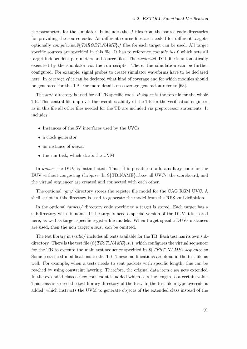
4.2. EXTOLL Functional Verification
the parameters for the simulator. It includes the .f files from the source code directories
for providing the source code. As different source files are needed for different targets,
optionally compile ius ${TARGET NAME}.f files for each target can be used. All target
specific sources are specified in this file. It has to reference compile ius.f, which sets all
target independent parameters and source files. The ncsim.tcl TCL file is automatically
executed by the simulator via the run scripts. There, the simulation can be further
configured. For example, signal probes to create simulator waveforms have to be declared
here. In coverage.cf it can be declared what kind of coverage and for which modules should
be generated for the TB. For more details on coverage generation refer to [63].
The src/ directory is used for all TB specific code. tb top.sv is the top file for the whole
TB. This central file improves the overall usability of the TB for the verification engineer,
as in this file all other files needed for the TB are included via preprocessor statements. It
includes:
• Instances of the SV interfaces used by the UVCs
• a clock generator
• an instance of duv.sv
• the run task, which starts the UVM
In duv.sv the DUV is instantiated. Thus, it is possible to add auxiliary code for the
DUV without congesting tb top.sv. In ${TB NAME} tb.sv all UVCs, the scoreboard, and
the virtual sequencer are created and connected with each other.
The optional rgm/ directory stores the register file model for the CAG RGM UVC. A
shell script in this directory is used to generate the model from the RFS xml definition.
In the optional targets/ directory code specific to a target is stored. Each target has a
subdirectory with its name. If the targets need a special version of the DUV it is stored
here, as well as target specific register file models. When target specific DUVs instances
are used, then the non target duv.sv can be omitted.
The test library in testlib/ includes all tests available for the TB. Each test has its own sub-
directory. There is the test file (${TEST NAME}.sv), which configures the virtual sequencer
for the TB to execute the main test sequence specified in ${TEST NAME} sequence.sv.
Some tests need modifications to the TB. These modifications are done in the test file as
well. For example, when a tests needs to sent packets with specific length, this can be
reached by using constraint layering. Therefore, the original data item class gets extended.
In the extended class a new constraint is added which sets the length to a certain value.
This class is stored the test library directory of the test. In the test file a type override is
added, which instructs the UVM to generate objects of the extended class instead of the
91
4. Functional Verification
Figure 4.35.: CAG Testbench Hierarchy
original one.
In testlib/ also a base test for all tests is stored. All tests are extended from this test.
The base test instantiates the UVM TB (${TB NAME} tb.sv) and includes functionality
that is used in all tests like printing the UVM topology. Thus, it possible to make changes
to all tests without modifying each single test, which increases the verification efficiency and
reduces duplicated code. In test lib.sv all tests are included with preprocessor statements.
This file gets included in tb top.sv. In seqlib/ sequences can be stored, that can be used by
all tests in the test library.
In the testlib/ directory a create new test.pl also exists, which creates a new test. As
parameter it needs the name of the new test. It makes a new directory with the test
name, creates the test and sequence files, and adds include statements for the new files to
test lib.sv. Afterward, the test can be started directly. The test writer only needs to fill
the test sequence with the intended test stimulus.
The vpm/ directory summarizes all files needed for the regression of the TB. In analysis/
there is the verification plan specific for this DUV. It instantiates the verification plan from
the UVCs used, the white box verification plan for the RTL and the code coverage. The
scripts/ directory is used for the run scripts needed for the regression environment. For a
detailed description see section 4.2.6 on page 133.
Figure 4.35 shows the TB hierarchy resulting from the described structure.
The definition of the directory structure enables it to create the infrastructure for a new
TB using a script, which significantly reduces the time needed to start a new TB. This
script is stored in the verification/tb/ directory of the SVN. It expects the name of the new
92
4.2. EXTOLL Functional Verification
Option Description
-h Prints the help.
-c Runs clean up.sh in the TB directory before startingthe simulator.
-t ${TEST NAME} Selects the test to run.
-v Sets the UVM verbosity.
-d ${TARGET NAME} Selects the target.
-g Opens the graphical waveform viewer.
-o Enables coverage generation.
-s ${SEED} Selects the seed for the random constraint solver.
-f Disables the execution of the pre run*.sh scripts.
Table 4.1.: Run Script Options
TB as a parameter and creates the whole directory structure including all files mandatory
for each TB. The newly created TB can be started immediately. The test writer then has
to fill this skeleton with the functionality required.
4.2.3.2. Testbench Run Script
Before the verification methodology described in this chapter was introduced at the CAG,
each TB used its own run script. These scripts had different options, and different methods
to select a test, when this was even possible. Each TB user needed to dig in the scripts to
get to know, how to use them. To simplify the use of the run scripts, a common run script
format for all TBs was developed.
The new run script is split into a TB independent core script and the run.sh script in the
TB itself. So, improvements made to the core script are available to all TBs immediately.
The TB run.sh script is a small wrapper for the core script. It controls the core script via
environment variables. It needs to set the path to the TB and optionally a default target,
and calls then the core script.
The core script starts the simulator. The runtime options for the simulator are specified
in either build/compile ius.f or build/compile ius ${TARGET NAME}.f, if the -d option
is set, of the TB. So, the run script instructs the simulator to use the options from the
compile file. Some IPs need to be compiled in a library before the simulator is started.
Therefore, optional pre run.sh scripts in the TB directory are used. The core script checks
their availability, and executes them if needed. It also possible to use target specific pre
run scripts, which must be called pre run ${TARGET NAME}.sh. They are called after
the common pre run script.
The -o instructs the simulator to collect coverage during simulation. The selecting of
93
4. Functional Verification
the coverage types that should be collected and for which modules can be made in the file
build/coverage.cf.
Table 4.1 lists all available run script options.
4.2.4. Unit Verification
For the verification of EXTOLL TBs for each major unit were created. As examples for
these TBs, this section describes the TBs for the RMA and the barrier. The RMA TB was
chosen because of its complexity. On the basis of the barrier, an example for the formal
verification is given.
4.2.4.1. RMA
The RMA functional unit is used in EXTOLL to realize remote memory access. An
overview of the RMA is given in section 4.2.2 on page 75. For the verification of the RMA
a verification plan was created first. There all features of the RMA were listed.
The verification environment needs to verify all features of the RMA. Therefore, it must
be able to create all legal and possible input stimulus on the one hand. On the other hand,
all transactions generated by the RMA and received by the verification environment must
be checked. First, it needs to be checked that a transaction generated by the RMA is
expected. These transactions are a result of a descriptor sent to the RMA before. The
RMA is not allowed to generate transactions, which do not have their origin in a descriptor
sent to the RMA before. Second, when the transaction is expected its fields must be
checked against the fields of the transaction generated by the reference model for the RMA
from the descriptor which caused the received transaction.
The RMA is connected to the other units by standard EXTOLL interfaces. It communi-
cates with the host via two HTAX interfaces. The first interface is shared by the requester
and the completer. The second one is connected to the responder. On the network side two
NP interfaces are used. They are connected to the RMA main units in the same way as
the HTAX interfaces. Beside these main interfaces, several other helper interfaces are used.
The BQ request interface connects to the RMA to the BQ. The BQ handles the the ring
buffers in main memory which are used by the RMA the store the notifications for each
VPID. The interface is used to request the next main memory address for a VPID. The
ATU interface is used to request address translations from the ATU. The RFS interface
connects the internal RF to the global EXTOLL RF.
For the stimulus generation for these interfaces there are two possibilities: Either create
one large UVC, which directly connects to the RMA’s interfaces, or create several UVCs,
94
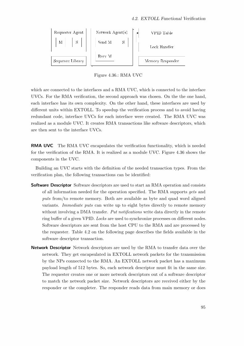
4.2. EXTOLL Functional Verification
Figure 4.36.: RMA UVC
which are connected to the interfaces and a RMA UVC, which is connected to the interface
UVCs. For the RMA verification, the second approach was chosen. On the the one hand,
each interface has its own complexity. On the other hand, these interfaces are used by
different units within EXTOLL. To speedup the verification process and to avoid having
redundant code, interface UVCs for each interface were created. The RMA UVC was
realized as a module UVC. It creates RMA transactions like software descriptors, which
are then sent to the interface UVCs.
RMA UVC The RMA UVC encapsulates the verification functionality, which is needed
for the verification of the RMA. It is realized as a module UVC. Figure 4.36 shows the
components in the UVC.
Building an UVC starts with the definition of the needed transaction types. From the
verification plan, the following transactions can be identified:
Software Descriptor Software descriptors are used to start an RMA operation and consists
of all information needed for the operation specified. The RMA supports gets and
puts from/to remote memory. Both are available as byte and quad word aligned
variants. Immediate puts can write up to eight bytes directly to remote memory
without involving a DMA transfer. Put notifications write data directly in the remote
ring buffer of a given VPID. Locks are used to synchronize processes on different nodes.
Software descriptors are sent from the host CPU to the RMA and are processed by
the requester. Table 4.2 on the following page describes the fields available in the
software descriptor transaction.
Network Descriptor Network descriptors are used by the RMA to transfer data over the
network. They get encapsulated in EXTOLL network packets for the transmission
by the NPs connected to the RMA. An EXTOLL network packet has a maximum
payload length of 512 bytes. So, each network descriptor must fit in the same size.
The requester creates one or more network descriptors out of a software descriptor
to match the network packet size. Network descriptors are received either by the
responder or the completer. The responder reads data from main memory or does
95
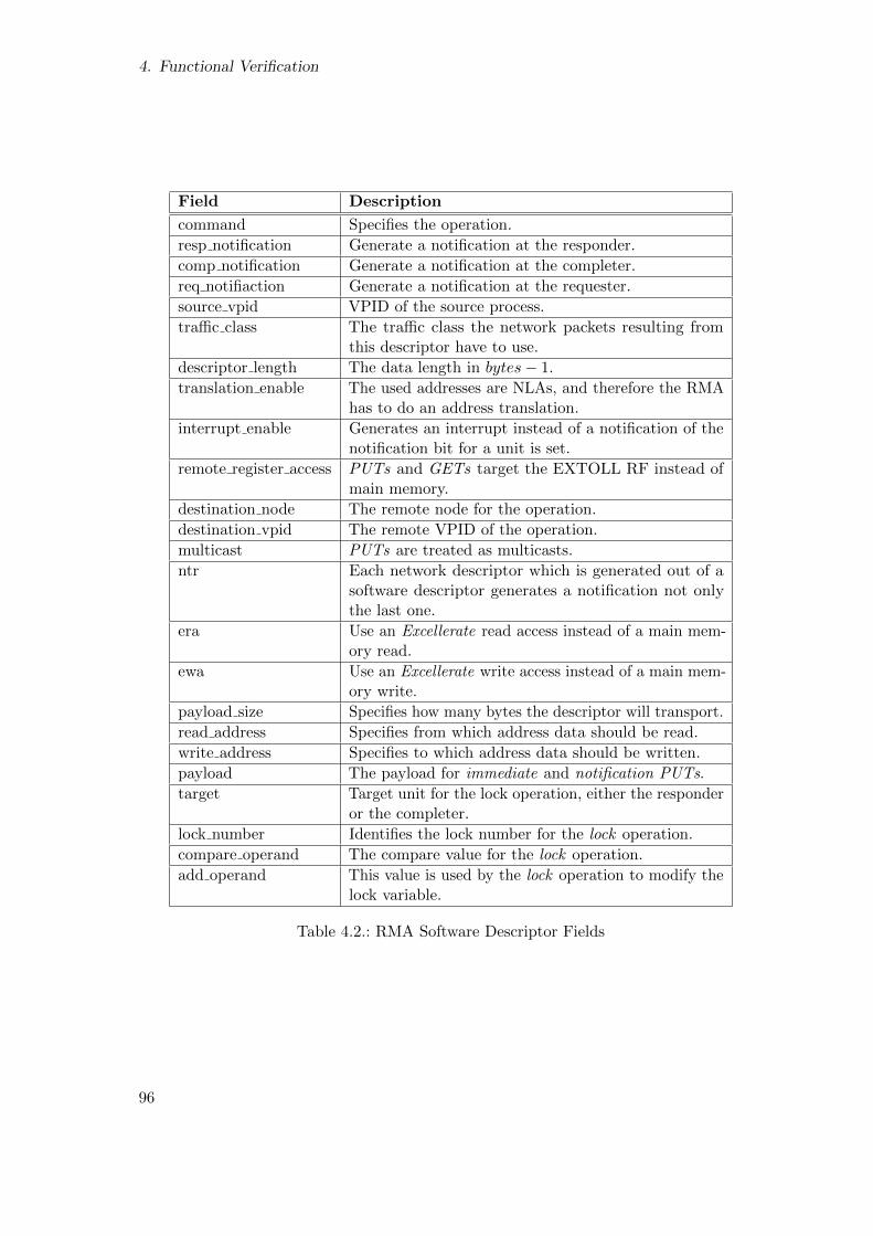
4. Functional Verification
Field Description
command Specifies the operation.
resp notification Generate a notification at the responder.
comp notification Generate a notification at the completer.
req notifiaction Generate a notification at the requester.
source vpid VPID of the source process.
traffic class The traffic class the network packets resulting fromthis descriptor have to use.
descriptor length The data length in bytes− 1.
translation enable The used addresses are NLAs, and therefore the RMAhas to do an address translation.
interrupt enable Generates an interrupt instead of a notification of thenotification bit for a unit is set.
remote register access PUTs and GETs target the EXTOLL RF instead ofmain memory.
destination node The remote node for the operation.
destination vpid The remote VPID of the operation.
multicast PUTs are treated as multicasts.
ntr Each network descriptor which is generated out of asoftware descriptor generates a notification not onlythe last one.
era Use an Excellerate read access instead of a main mem-ory read.
ewa Use an Excellerate write access instead of a main mem-ory write.
payload size Specifies how many bytes the descriptor will transport.
read address Specifies from which address data should be read.
write address Specifies to which address data should be written.
payload The payload for immediate and notification PUTs.
target Target unit for the lock operation, either the responderor the completer.
lock number Identifies the lock number for the lock operation.
compare operand The compare value for the lock operation.
add operand This value is used by the lock operation to modify thelock variable.
Table 4.2.: RMA Software Descriptor Fields
96
4.2. EXTOLL Functional Verification
a lock operation and sends the responses as network descriptors to the completer
of the source node. The completer writes the data attached of a received network
descriptor into the main memory. The fields of the network descriptor are shown in
table 4.3 on page 97.
Memory Access Memory accesses are used by the RMA to read and write data from/to
main memory. The requester and the responder do read accesses to receive data from
main memory, which is then injected into the network. The completer uses write
accesses to store data received from the network in main memory. There are three
different access types: read, write, and read response. Table 4.4 shows all fields of
the memory access.
Notification Notifications are used to inform the software, that a RMA operation has
finished. Each software or network descriptor can trigger a notification depending on
the notification fields of the software descriptor, which started the RMA operation.
The notifications are written to a ring buffer in main memory, which is handled by
the BQ. There are three different notification types: standard notifications, which
are used by put and get commands. Notification puts are special puts to write data
directly in the notification ring buffer, and thus they have an own format. Lock
notifications carry information to identify the lock number and the result of a lock
operation. Table 4.5 on the next page lists all notification fields.
For each transaction, an UVM transaction was defined by extending uvm sequence item.
This way, the transactions are provided automatically with print, compare, and copy
functions which operate on all transaction fields. The pack and unpack UVM callbacks
were used to implemented the according pack and unpack functionality for each transaction.
These functions are used to create a bit stream out of a transaction and the other way
round. They simplify the transformation of a transaction to a bit pattern in the driver.
As the transactions are created randomly, it can happen, that transaction fields are
assigned values which are out of their allowed ranges. For example, the allowed range for
the payload length is different for each descriptor command. To assist the random solver,
which assigns the random values to the fields of the transactions, constraints are used,
which define allowed values for each field. For each transaction, default constraints were
added to create valid default random transactions. These constraints need to be as general
as possible, to allow the generation of all possible input stimulus. For a more specialized
test, these constraints can be modified be by the test writer.
The RMA UVC must be able to generate stimulus for each unit of the RMA. First,
it has to generate software descriptors for the requester. Second, it also has to generate
network descriptors for the responder and the completer. Therefore, two different agents
were developed. The requester agent handles the software descriptors. The network agent
97
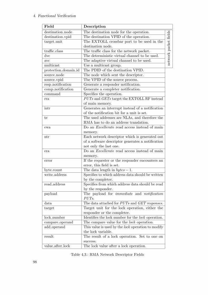
4. Functional Verification
Field Description
destination node The destination node for the operation.
net
work
pac
ket
fiel
ds
destination vpid The destination VPID of the operation.target unit The EXTOLL crossbar port to be used in the
destination node.traffic class The traffic class for the network packet.dvc The deterministic virtual channel to be used.avc The adaptive virtual channel to be used.multicast Use a multicast group.
protection domain id The PDID of the destination VPID.source node The node which sent the descriptor.source vpid The VPID of the source process.resp notification Generate a responder notification.comp notification Generate a completer notification.command Specifies the operation.rra PUTs and GETs target the EXTOLL RF instead
of main memory.intr Generates an interrupt instead of a notification
of the notification bit for a unit is set.te The used addresses are NLAs, and therefore the
RMA has to do an address translation.ewa Do an Excellerate read access instead of main
memory.ntr Each network descriptor which is generated out
of a software descriptor generates a notificationnot only the last one.
era Do an Excellerate read access instead of mainmemory.
error If the requester or the responder encounters anerror, this field is set.
byte count The data length in bytes− 1.write address Specifies to which address data should be written
by the completer.read address Specifies from which address data should be read
by the responder.payload The payload for immediate and notification
PUTs.data The data attached for PUTs and GET responses.target Target unit for the lock operation, either the
responder or the completer.lock number Identifies the lock number for the lock operation.compare operand The compare value for the lock operation.add operand This value is used by the lock operation to modify
the lock variable.result The result of a lock operation. Set to one on
success.value after lock The lock value after a lock operation.
Table 4.3.: RMA Network Descriptor Fields
98
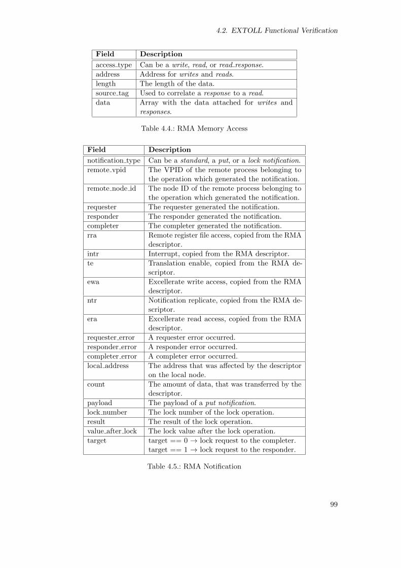
4.2. EXTOLL Functional Verification
Field Description
access type Can be a write, read, or read response.
address Address for writes and reads.
length The length of the data.
source tag Used to correlate a response to a read.
data Array with the data attached for writes andresponses.
Table 4.4.: RMA Memory Access
Field Description
notification type Can be a standard, a put, or a lock notification.
remote vpid The VPID of the remote process belonging tothe operation which generated the notification.
remote node id The node ID of the remote process belonging tothe operation which generated the notification.
requester The requester generated the notification.
responder The responder generated the notification.
completer The completer generated the notification.
rra Remote register file access, copied from the RMAdescriptor.
intr Interrupt, copied from the RMA descriptor.
te Translation enable, copied from the RMA de-scriptor.
ewa Excellerate write access, copied from the RMAdescriptor.
ntr Notification replicate, copied from the RMA de-scriptor.
era Excellerate read access, copied from the RMAdescriptor.
requester error A requester error occurred.
responder error A responder error occurred.
completer error A completer error occurred.
local address The address that was affected by the descriptoron the local node.
count The amount of data, that was transferred by thedescriptor.
payload The payload of a put notification.
lock number The lock number of the lock operation.
result The result of the lock operation.
value after lock The lock value after the lock operation.
target target == 0 → lock request to the completer.target == 1 → lock request to the responder.
Table 4.5.: RMA Notification
99

4. Functional Verification
creates network descriptors. Each agent has a sequencer, which is able to create descriptors.
The requester agent has one monitor, which samples the software descriptors sent to the
DUV. The network agent has two monitors, as on the network port interface packets are
sent to the NP and received from the NP. Consequently, it possible to distinguish between
packets sent in a direction more easily.
Because the RMA uses DMA, main memory must be provided in its verification environ-
ment. It is not practical to provide a complete memory in the verification environment.
This memory has to be allocated in advance to a test run, and needs a lot of physical
memory, while only a small amount of memory is actually used. The reduced size makes it
also impossible to use high and low memory addresses in the same test, which narrows the
test coverage. Instead of using a real memory, the memory gets emulated in the verification
environment. This emulation is done by the memory responder of the RMA UVC. The
RMA forwards the data read from main memory to the network and has no constraints
about its content. Thus, it is sufficient, when the verification environment returns complete
random data for a read request. Therefore, read requests are forwarded to the memory
responder. It then creates a responds with random data attached, which is sent to the
RMA in return.
The RMA uses a VPID table to store VPID specific information. There it stores data
like if a VPID is enabled or its PDID. Before the RMA can process traffic, this table must
be initialized. The UVC needs also to handle this table. It has to do its initialization and
checks received descriptors with the help of table. This functionality is implemented in the
VPID table component of the UVC. It implements a list of table entries. Each entry has
all fields which are needed for a VPID. Theses entries are randomized in the beginning of
a test. Getter and setter functions can be used by any verification component to access
these entries. The verification environment uses an initialization sequence to write the
table into the RMA.
The RMA supports a lock operation using an atomic fetch-compare-and-add operation.
The operation itself is handled in the RMA to ensure its atomicity. The lock values for
each lock number are located in main memory and cannot be used on user-defined data.
The management of the locks in the verification environment is done by the lock handler.
It abstracts the main memory region, which is used in a real system for locks. All available
lock values are stored in an internal array. Getter and setter functions are used to access
the lock values from other verification components. A get address function returns the
address for a given VPID lock number combination.
The RMA UVC’s sequence library includes basic sequences which assists the UVC user
with the stimulus generation for the RMA. Following sequences are available:
Send Software Descriptor The send software descriptor sequence sends a single software
100

4.2. EXTOLL Functional Verification
descriptor. The command field of the software descriptor to be sent is constraint to
valid requester commands.
Send Network Descriptor The send network descriptor sequence sends a single network
descriptor and must be executed on the sequencer of the network agent. Its single
field is the network descriptor to be sent. Each network descriptor sent to the RMA
must carry the same PDID as stored in the RMA’s VPID table. If they do not equal,
the RMA drops the received descriptor. The sequence ensures, that the descriptor is
sent with the right PDID. Therefore, the network descriptor gets randomized first.
Afterward, the right PDID for its destination VPID gets inserted. Last, the sequence
sends the network descriptor.
Send Responder Descriptor The send responder descriptor sequence inherits from the
send network descriptor sequence. It adds a constraint, that only valid responder
commands are sent by this sequence.
Send Completer Descriptor The send completer descriptor sequence inherits from the
send network descriptor sequence. It adds a constraint, that only valid completer
commands are sent by this sequence.
TB After all required UVCs for the RMA verification were finished, the RMA TB was
build. An overview of the TB is given in figure 4.37 on the following page. It shows the
UVCs used and the connections between them.
First, the directory structure for the TB as described in section 4.2.3.1 on page 87
was created followed by the instantiation of the DUV. The DUV also includes an HTAX
instance. The HTAX is used as in the complete EXTOLL. It provides three different ports,
where each one is used for a single HT VC. These ports are connected the the HTAX
bridge within EXTOLL. In the TB these ports are used to connect the UVCs to the RMA,
which simplifies the handling of the VCs in the TB a lot.
The next step was to connect the SV interfaces, which are used by the UVCs to interact
with the DUV. Followed by the instantiation of the UVCs. First the interface UVCs were
created and instantiated and configured. For the HP2NP UVCs only the slave agents
were activated, as they receive packets from the RMA and do not inject any packets. The
NP2HP UVCs sent packets to the DUV and do not receive any of them, so the master
agents were activated and the slave agents deactivated. The ATU UVC has to respond
to ATU translation requests. Therefore, only the RMA slave agent needs to be activated
for the ATU UVC. The RGM UVC sends RF requests to the RMA. There, the master
agent is activated. The BQ UVC has to respond to BQ address requests. So, the request
slave agent is activated. There, also the host agent is set to passive. It is used to receive
the RMA’s notifications and checks that they are written to the right memory location of
101

4. Functional Verification
Figure 4.37.: RMA TB Overview
102
4.2. EXTOLL Functional Verification
its related ring buffer. The UVC for the posted VC needs to send packets to the RMA
and receive posted writes from the DUV. There, the master agent for the included HTAX
Transmit (TX) UVC and the slave agent for the HTAX Receive (RX) UVC are activated.
On the non posted HT VC, the verification environment has to receive requests from the
DUV, but has not to sent its own. Here, only the HTAX RX UVC slave agent is required.
For the response VC the TB sends requests to the RMA, but does not receive them from
the DUV. Thus, the master of HTAX TX UVC is activated.
After the DUV was connected to the interface UVCs, the RMA UVC was integrated into
the TB. For this integration, the method for connecting UVCs described in section 4.1.7.6
on page 72 was used. First, new extended sequencers for all interface sequencers were
created. They obtained an UVM pull port for receiving data item from higher level
sequencers. Then translation sequences, which create interface UVC transaction out of the
RMA transactions, were constructed. Type overrides in the TB made sure, that the new
sequencers were used instead of the original ones. The upper and lower level sequencers
were connected in the TB as well. Following sequencers were modified this way:
• The HyperTransport on Chip Protocol (HTOC) master sequencer of posted HTOC
UVC instance.
• The HTOC master sequencer of response HTOC UVC instance.
• The NP2HP master sequencer of the first NP2HP UVC instance.
• The NP2HP master sequencer of the second NP2HP UVC instance.
In order to connect the monitors of the RMA UVC to the scoreboard, the monitors
need to receive transactions from the interface monitors. Then, the RMA UVC monitors
transform the interface transactions into RMA descriptor transactions. Therefore, the
RMA monitors were extended as described in section 4.1.7.6 on page 72. Type overrides
for the RMA monitors were added to the TB to use the new extended monitors instead
of the original ones. The connections between the interface and RMA monitors were also
established in the TB.
All RMA units access main memory. Following operation are executed:
• Read accesses for DMA by the requester and the responder.
• Write accesses for DMA by the completer.
• Notifications are stored in main memory ring buffers using memory writes.
• The lock values needed for lock operations are stored there and are access by reads
and writes.
By doing so, for the verification arises the problem that it cannot distinguish the
103
4. Functional Verification
functionality that is targeted by a write access, which is needed in the scoreboard to decide
which checks must be applied for a write. Writes can either trigger data checks for the
completer, notification checks for ring buffers accesses, or lock operation checks. The first
possible solution for this problem is to search the different queues for expected items in the
scoreboard to find the target functionality. This solution is very complicated to implement
in the scoreboard, as it adds more complexity to the already complex scoreboard. That’s
why another solution was chosen. For the addresses for writes into main memory a memory
map is used. The address space is divided into three segments: the lock, the completer,
and the buffer queue segment. As current CPUs have a maximum physical address size
of 52 Bits, the address bits 51 to 50 are used as a segment tag. In the build phase of the
TB the segment tags are randomized, in order that each segment is mapped to the each
address range. This information is stored in the configuration object of the TB and is used
by the scoreboard to correlate a received write to a function block. Also, all descriptors
sent to the RMA need to be aware of these segments.
The descriptors’s fields send to the RMA cannot be completely randomized. They have
to follow TB specific constraints like the address constraints for writes which are sent
by the RMA. Indeed, these writes are sent by the RMA, but they have their origin in a
descriptor sent before by the TB. So, each descriptor has to be constraint in a way, that
all resulting RMA transactions fulfill the global constraints as well.
Another point a test writer has to keep in mind are the translations for NLAs. When the
NLAs for a descriptor are generated completely random, there is no translation available
in the beginning, as the GAT table of the RMA UVC is empty when the simulation starts.
Therefore, a new GAT entry must be created for the NLA before the descriptor is sent
to the DUV. Send sequences were written for the TB which add GAT entries before the
descriptors.
To hide some constraints from the test writer and therefore make it easier to create valid
descriptors, the following sequences are available in the TB:
Send software descriptor sequence The send software descriptor sequence sends a single
software descriptor. It inherits from the software descriptor sequence of the RMA
UVC. It automatically adds valid address translations to the GAT table of the TB,
after the descriptor was randomized and before it is sent to the RMA.
Send responder descriptor sequence The send responder descriptor sequence sends a
single network descriptor. It inherits from the send responder descriptor sequence of
the RMA UVC. It automatically adds valid address translations to the GAT table of
the TB, after the descriptor was randomized and before it is sent to the RMA.
Send completer descriptor sequence The send completer descriptor sequence sends a
single network descriptor. It inherits from the send completer descriptor sequence of
104

4.2. EXTOLL Functional Verification
Figure 4.38.: RMA User Sequences
the RMA UVC. It automatically adds valid address translations to the GAT table of
the TB, after the descriptor was randomized and before it is sent to the RMA. In
addition, it has a constraint, that ensures, that the descriptor’s write address hits
the current memory segment of the completer.
Send responder descriptor with wrong PDID sequence The send responder descriptor
with wrong PDID sequence sends a single network descriptor. It can be used to
verify the error handling of the RMA. It inherits from the send responder descriptor
sequence of the TB and overrides the set protoction domain id() function inherited
from the send network descriptor sequence of RMA UVC to return a wrong PDID.
The probability for a wrong PDID is controlled by a constraint.
Send completer descriptor with wrong PDID sequence The send completer descriptor
with wrong PDID sequence sends a single network descriptor. It can be used to
verify the error handling of the RMA. It inherits from the send completer descriptor
sequence of the TB and overrides the set protoction domain id() function inherited
from the send network descriptor sequence of RMA UVC to return a wrong PDID.
The probability for a wrong PDID is controlled by a constraint.
Before the TB can sent descriptors to the RMA, the RMA has to be initialized. This is
done by an initialization sequence, that writes into the RF of the RMA using the CAG
Register Modeling (RGM) UVC. The values of the configured parameters are stored in the
global configuration object of the UVC. The sequence is executed by each test in the run
phase, before it starts to sent the test specific stimulus. The initialization sequence itself
105
4. Functional Verification
executes a couple of function specific sequences. The following sub initialization sequences
are used:
General Configuration The general configuration sets the network Maximum Transfer
Unit (MTU), and the PCIe MTU.
VPID Table initialization This sequence initializes the VPIDs in the RMA. It writes all
available VPID table entries of the RMA UVC’s VPID table to the RMA. The table
itself is initialized during the TB’s end of elaboration phase.
Buffer Queue Initialization The buffer queue initialization sequence creates the descriptor
queues for the buffer queue. The size of each ring buffer and the number of buffer
segments are randomized and stored in the BQ UVC.
Lock Initialization The lock initialization sequence writes the base address of the lock
memory segment. It also writes the lock configuration register, which enables the
locks, set the number of available VPIDs, and the number of available locks per
VPID.
RMA Scoreboard The checking of the RMA’s the the black box behavior is done by the
TB’s scoreboard. It generates for each descriptor sent to the RMA by the TB the expected
response transactions. These response transactions are stored in the scoreboard. Each
transaction generated by the RMA is forwarded to the scoreboard. The scoreboard checks,
if the transaction is expected. If not a error message is printed, otherwise the fields of the
expected transaction are compared against the fields of the expected one. If there is any
mismatch an error message is reported. When an error is detected by the scoreboard, it
stops the simulation immediately, as from this point on the DUV is in a error state and
may behave not correctly any more.
As described in the previous sections, all interfaces of the RMA are monitored by UVCs.
Via UVC layering all transactions generated by the RMA are transformed into RMA UVC
transactions. The monitors of the UVCs are used to forwarded these transactions to the
scoreboard. The connections between the scoreboard and the monitors are established
via UVM TLM channels. The RMA UVC monitors forward all software and network
descriptors sent to and from the RMA. Beside these connections all read and write memory
accesses as well as all buffer queue accesses are forwarded to scoreboard. All monitor to
scoreboard connections are shown in figure 4.37 on page 102.
All three RMA units operate independently of each other. For example, when the
requester sends a get operation it hasn’t to wait for a response from the responder. So, the
scoreboard can check the units independent of the other units as well.
The scoreboard needs to store the expected RMA transactions for a descriptor until
106
4.2. EXTOLL Functional Verification
the DUV sends a response. Each expected transaction must be easily correlated to its
original descriptor to be able to determine when an RMA operation is finished. So, it
is not feasible to use a set of queues for expected network descriptors, memory accesses
and so on. As the expected transactions must be correlated to a descriptor, another
possibility would be to extend the RMA descriptors by several fields to store the expected
transactions. This reduces the re-useability of the scoreboard, when global factory type
overrides for descriptors are used. That’s why a third solution was chosen. For all RMA
units a scoreboard container object was created. These containers store all information
needed by the scoreboard to check the processing of a single descriptor. Each descriptor
sent to the RMA gets an own container instance. The RMA’s units process all received
descriptors in order. So, the scoreboard has container queues for each unit, where the
descriptors are stored in order. Not until the first descriptor in a queue is finished, the
next one is checked.
Requester Checking The requester is checked by the scoreboard in the following way.
The scoreboard receives software descriptors sent to the RMA from the RMA UVC’s request
monitor. It creates a request scoreboard container and adds the received descriptor. For put
operations the requester needs to read data from main memory. Therefore, the scoreboard
generates the expected reads. If an address translation is requested by the descriptor, the
scoreboard requests the physical address for the descriptors read address from the ATU
UVC. When more than one page must be read because of the descriptors length, also
the translations for the following pages are requested. Then the addresses and sizes of
the all read requests are calculated, and stored in the container. Puts and gets operation
send more than one network descriptor. For this reason, also the addresses of the network
descriptors are calculated and stored in the container. For all other operations, the requester
generates one network descriptor for each received network descriptor, and copies the fields
of the software descriptor to the according fields of the network descriptor. Therefore, the
scoreboard stores the newly created container in the container of the requester without
any further action.
When a main memory read request is received, its address is compared against the
expected address of the first container which expects a read. If the address matches the
expected address is set to the next address, otherwise an error is reported. When response
for this request is received, its data is attached to the first container which expects a read
for a later data check.
When the scoreboard receives a network descriptor sent by the requester, it checks if a
software descriptor is outstanding in the container queue. If not an error is reported. When
a software descriptor is available, first all fields that copied from the software to the network
descriptor are checked. Afterward, the network descriptor addresses are compared with
107
4. Functional Verification
the expected ones, as well as the data which was received by the scoreboard with memory
responses. If no more network descriptors are expected, the current scoreboard container is
deleted. If not, the address and data pointers are incremented in the container for the next
network descriptor. If it was the last network descriptor for a software descriptor and the
software descriptor has to generate a notification, the container is added to a notification
queue for further checking.
Responder Checking The completer performs two actions. First, it reads data for
get requests from main memory and generates get responses. Second, it processes lock
operations.
The scoreboard receives network descriptors sent to the responder from the send monitor
of the RMA UVC’s second network agent. Each network descriptor is stored in its own
scoreboard container. For get requests, the scoreboard has to calculated the expected
memory read accesses. If the read address in the network descriptor is an NLA, the
scoreboard requests the physical addresses for each page that is targeted by the descriptor
from the GAT of the ATU UVC. Thereafter, The addresses and sizes for each expected
memory read request are calculated and stored in the container. The container is add to
the responder container queue. When the responder starts to read from main memory,
the scoreboard receives the read requests from the memory responder of the RMA UVC.
It then compares the addresses and sizes of the requests with the expected ones from
the first responder container entry expecting read requests. If there are mismatches an
error is reported. The data of the responses generated by the TB, are forwarded to
scoreboard by the TB’s memory monitor. The scoreboard adds the data to the first
responder container with outstanding memory requests. When the responder has read
all data from main memory, it creates a get response descriptor and injects it into the
network. This descriptor is forwarded to the scoreboard by the receive monitor of the
RMA UVC’s second network agent. This descriptor’s fields are compared to the fields of
the first descriptor in the scoreboard’s responder queue. Also data is checked against the
collected data from the memory responses received before. If there are no mismatches, the
first container is removed from the responder queue. Otherwise an error is reported. If
the request descriptor indicates, that the responder has to trigger a notification after the
completion, the container is added to the notification queue for further checking.
For a lock operation, the responder reads the lock value from main memory, and compares
the lock value with the compare value in the network descriptor. If the lock value is less or
equal the compare value, the lock is successful. In this case, the responder adds the add
value of the descriptor to the lock value and writes the new lock value into main memory.
After the completion of the lock operation, lock response is set the node which requested
the lock. It carries the result of the lock operation and the current lock value.
108
4.2. EXTOLL Functional Verification
When the scoreboard receives a lock operation, it generates the lock address from the
lock number and the VPID, and adds this address to the scoreboard container. On the
responder’s read of the lock value from main memory, the read address is compared with
the expected one of the container. The data of the response is stored in the container.
When the scoreboard receives the lock response, it compares the fields of response with
the fields of the lock request. As the scoreboard has the value of the old lock value stored
from the memory response, it can check the lock value and the result in the lock response.
Afterward, the first container is removed from the responder queue. If notification should
be sent, the container is added to the notification queue.
Completer Checking The scoreboard receives network descriptors sent to the completer
from the send monitor of the RMA UVC’s first network agent. As for the other units, a
scoreboard container is created for the received descriptor. For puts and get responses, the
completer writes the data attached to the descriptor into the main memory. Therefore,
the scoreboard calculates the addresses, and sizes for the expected memory write requests
using the write address of the descriptor as start address. If the write address is an NLA,
an address translation with the help of the GAT is done for each page that is hit by the
current descriptor to get the physical address. The addresses and sizes are stored in the
container. Lock responses only generate notifications. That’s why in this case the container
is directly added to notification queue instead of the completer one.
When the scoreboard receives a memory write targeting the completer’s memory segment,
the write’s address, size and data are compare to the expected values of the first completer
container in the completer queue. If all writes for a descriptor were seen, its container is
removed from the queue. If the descriptor requests a notification, the container is added to
the notification queue.
The NP2HP monitors as all monitors collect a complete packet, before they sent the
transaction for this packet to other UVM components. The completer starts the descriptor
processing immediately after it receives its the first word. Due to the short completer
pipeline, it can happen therefore, that it sends the first write before the scoreboard receives
the corresponding descriptor. If this is not considered the scoreboard would report an error,
as it can’t assign a descriptor to this write. To solve this problem, the scoreboard has an
extra queue, where writes are stored, for which the network descriptor wasn’t seen yet.
When scoreboard receives a descriptor, and the write queue isn’t empty the writes in the
queue are compared with the expected one of the descriptor. As they must be triggered by
this descriptor, an error is reported on mismatch. This repeated until the queue is empty.
Notification Checking Notification are written to a BQ ring buffer. The buffer for each
VPID is shared among the RMA units. From this it follows, that the notifications for an
109

4. Functional Verification
unit must have the same order in the buffer as the descriptors which have triggered the
notification. The notifications of from the units can be mixed.
Notifications can be sent by the RMA, after it has completed a descriptor. For the
checking of the notification the scoreboard needs the fields of the descriptor. That’s why,
all containers of descriptors, that generate a notification are moved to a notification queue
after the scoreboard has detected that the descriptor is completed.
The scoreboard receives notifications via the host monitor of the BQ UVC. If the
notification queue is empty, an error is reported. Each notification has a field indicating
by which unit it was sent. This information is used to find the according container in the
notification queue. If no container can be found, an error is reported. Else ways, the fields
of the notification and its descriptor are compared.
RMA Error Checking The RMA has to deal with different issues that are caused by
programming errors or an unexpected termination of a program. The behavior of the RMA
has to be verified in these situations as well, as they can occur quite often. The following
classes of errors can be distinguished:
Wrong PDID PDIDs are used by the RMA to prevent a process to read or write data
from another process from which it isn’t allowed to communicate with. The system
software sets the PDIDs for all VPIDs, that communicate with each other to the same
random value. The PDID for a VPID is stored in the RMA’s VPID table. When
the RMA injects a descriptor into the network, it adds the PDID of the descriptor’s
VPID to the descriptor. When the RMA receives a network descriptor, it compares
the received PDID with the target VPID’s PDID. The descriptor is only processed,
if the PDIDs match. If they don’t match, the RMA has to completely discarded this
descriptor, in that way that the descriptor doesn’t issue any further actions on this
node, disregarding optinla error notifications.
To verify the PDID handling, the TB needs to generate network descriptors with a
wrong PDID. For sending network descriptors, the TB provides sequences, which
add the correct PDID to a network descriptor before it is sent. These sequences were
extended to insert a random PDID instead of the right one. Whether a correct or a
wrong PDID is used, is randomized each time a descriptor is sent. The test writer
can control this via a constraint.
As the RMA has to drop the descriptor, without requesting any page translations,
accessing main memory, or generating notifications, the scoreboard drops a received
descriptor with a non matching PDID. If the RMA, doesn’t discard the descriptor
correctly, it will generate transactions on its interfaces. These transactions will trigger
an error, in the scoreboard, either because there are no outstanding transactions
110

4.2. EXTOLL Functional Verification
expected or because of a mismatch with other expected transactions.
Disabled VPID When the RMA receives any descriptor, which targets a VPID, that is
not enabled in the VPID table of the RF, the descriptor has to be discarded.
The TB verifies this by not enabling all VPIDs during the initialization. It still sends
random descriptors to all VPIDs. When the scoreboard receives a descriptor targeting
a not enabled VPID, it is discarded. If the RMA doesn’t drop the descriptor correctly,
it will generate transactions, which the scoreboard can’t correlate to descriptor, and
will therefore trigger an error.
Address Translation Failure The third error the RMA has to deal with are address trans-
lation failures. They are caused by programming failures. Either by addressing a
wrong NLA or by an unexpected termination of a program on a node, while other
nodes still access its data. When a program terminates, the EXTOLL kernel driver
frees its resources, which includes to delete the address mappings of the ATU used by
this program. If there are network descriptors still in flight in the network after the
clean up, the address translation isn’t available any more. The RMA must handle
these errors, as they can happen quite often during the development of a parallel
program.
The RMA TB uses send sequences, which add random address translations for a
descriptor to the GAT before it is sent. To verify the address translation failure
handling, the TB has to return no address translations for a translation request
randomly. Therefore, the descriptor send sequences were extended to randomly not
create one or more GAT entries for a descriptor, as a RMA descriptor can caused
memory accesses to one or more pages in main memory.
When the RMA requests a translation for NLA, that isn’t available, the ATU UVC
returns an invalid response indicating that there is no translation available.
The checking of the RMA’s behavior in the case of a non available translation is more
complex than in the first two failure cases. The translation can fail for the first or
any following page that is involved in a descriptor operation. When the translation
for the first page fails, no memory accesses are done. When the translation fails for
any following page, only the memory accesses for pages with a translation are done.
All following accesses aren’t executed. The scoreboard has to consider this when it
calculates the expected memory accesses. During the generations of the expected
memory accesses, it stops to add more accesses, if the GAT has no translation
for a page. Also, the network descriptors generated by the RMA look different.
When the translation for the first page fails, only the first network descriptor is sent
with no data attached and the error field set. Then the scoreboard adds only one
network descriptor as expected to the scoreboard container for this operation. If
111
4. Functional Verification
the translation fails for any later page, not all data can be read from main memory.
Then only the descriptors are sent, for which data can be read. The last descriptor
sent has a reduced size, if the data from this descriptor crosses a page boundary. As
the scoreboard knows for which page translations are available, it can calculate the
length of the last descriptor.
After all expected transactions are added to the scoreboard container of the received
descriptor with the modified calculations, the scoreboard does its checking as without
injected errors.
Test Library For the RMA TB a test library was created to verify the features of the
RMA more easily. Each test creates traffic, which is constraint to verify a specific feature or
several features. Theses tests are also used a regression, were they are executed repeatedly
each time with a different seed for the constraint solver.
The following tests are available:
Simple Test This test sends 100 packets to each RMA unit. It is meant to have a short
test to do a fast check if everything is still fine after changes to the RTL or TB code.
It is not intended for a use in the regression suite.
Requester The requester test only creates traffic for the requester. It sends 2000 random
software descriptors to the RMA. For sending the descriptors, the send software
descriptor sequence of the sequence library is used.
Responder The responder test only creates traffic for the responder. It sends 2000 random
network descriptors to the RMA. For sending the descriptors, the send responder
descriptor sequence of the sequence library is used.
Completer The completer test only creates traffic for the completer. It sends 2000 random
network descriptors to the RMA. For sending the descriptors, the send completer
descriptor sequence of the sequence library is used.
Random Traffic The random traffic test creates traffic for all RMA units simultaneously.
It sends 2000 random descriptor for each unit. For sending the descriptors, again the
according sequences from the sequence library are used.
Disabled VPID The disabled VPID test sends random traffic for all units. During the
initialization of the test a random count of VPIDs are not enabled. The TB sends
traffic for all VPIDs including the not enabled ones. This way, it can be verified that
the RMA correctly drops descriptors for disabled VPIDs.
Wrong Protection Descriptor This test is used to verify the RMA’s behavior, when it
receives network descriptors with wrong PDIDs. It sends random traffic for all units.
112
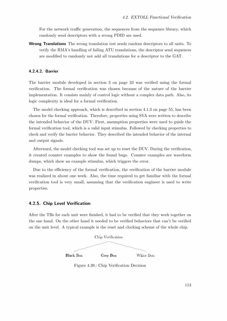
4.2. EXTOLL Functional Verification
For the network traffic generation, the sequences from the sequence library, which
randomly send descriptors with a wrong PDID are used.
Wrong Translations The wrong translation test sends random descriptors to all units. To
verify the RMA’s handling of failing ATU translations, the descriptor send sequences
are modified to randomly not add all translations for a descriptor to the GAT.
4.2.4.2. Barrier
The barrier module developed in section 3 on page 33 was verified using the formal
verification. The formal verification was chosen because of the nature of the barrier
implementation. It consists mainly of control logic without a complex data path. Also, its
logic complexity is ideal for a formal verification.
The model checking approach, which is described in section 4.1.3 on page 55, has been
chosen for the formal verification. Therefore, properties using SVA were written to describe
the intended behavior of the DUV. First, assumption properties were used to guide the
formal verification tool, which is a valid input stimulus. Followed by checking properties to
check and verify the barrier behavior. They described the intended behavior of the internal
and output signals.
Afterward, the model checking tool was set up to reset the DUV. During the verification,
it created counter examples to show the found bugs. Counter examples are waveform
dumps, which show an example stimulus, which triggers the error.
Due to the efficiency of the formal verification, the verification of the barrier module
was realized in about one week. Also, the time required to get familiar with the formal
verification tool is very small, assuming that the verification engineer is used to write
properties.
4.2.5. Chip Level Verification
After the TBs for each unit were finished, it had to be verified that they work together on
the one hand. On the other hand it needed to be verified behaviors that can’t be verified
on the unit level. A typical example is the reset and clocking scheme of the whole chip.
Figure 4.39.: Chip Verification Decision
113
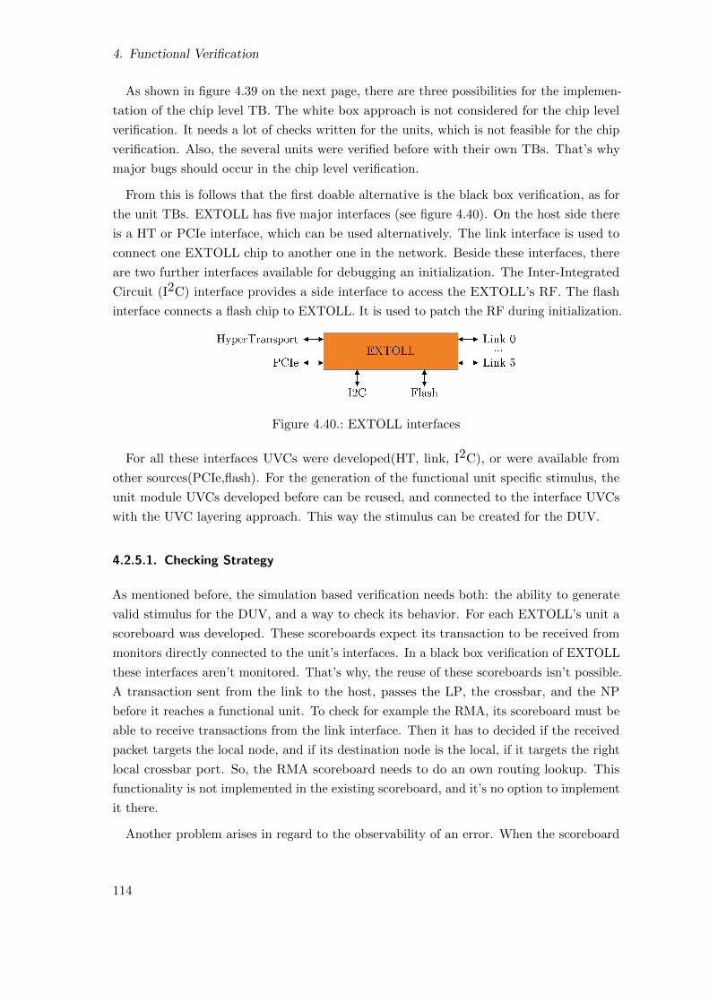
4. Functional Verification
As shown in figure 4.39 on the next page, there are three possibilities for the implemen-
tation of the chip level TB. The white box approach is not considered for the chip level
verification. It needs a lot of checks written for the units, which is not feasible for the chip
verification. Also, the several units were verified before with their own TBs. That’s why
major bugs should occur in the chip level verification.
From this is follows that the first doable alternative is the black box verification, as for
the unit TBs. EXTOLL has five major interfaces (see figure 4.40). On the host side there
is a HT or PCIe interface, which can be used alternatively. The link interface is used to
connect one EXTOLL chip to another one in the network. Beside these interfaces, there
are two further interfaces available for debugging an initialization. The Inter-Integrated
Circuit (I2C) interface provides a side interface to access the EXTOLL’s RF. The flash
interface connects a flash chip to EXTOLL. It is used to patch the RF during initialization.
Figure 4.40.: EXTOLL interfaces
For all these interfaces UVCs were developed(HT, link, I2C), or were available from
other sources(PCIe,flash). For the generation of the functional unit specific stimulus, the
unit module UVCs developed before can be reused, and connected to the interface UVCs
with the UVC layering approach. This way the stimulus can be created for the DUV.
4.2.5.1. Checking Strategy
As mentioned before, the simulation based verification needs both: the ability to generate
valid stimulus for the DUV, and a way to check its behavior. For each EXTOLL’s unit a
scoreboard was developed. These scoreboards expect its transaction to be received from
monitors directly connected to the unit’s interfaces. In a black box verification of EXTOLL
these interfaces aren’t monitored. That’s why, the reuse of these scoreboards isn’t possible.
A transaction sent from the link to the host, passes the LP, the crossbar, and the NP
before it reaches a functional unit. To check for example the RMA, its scoreboard must be
able to receive transactions from the link interface. Then it has to decided if the received
packet targets the local node, and if its destination node is the local, if it targets the right
local crossbar port. So, the RMA scoreboard needs to do an own routing lookup. This
functionality is not implemented in the existing scoreboard, and it’s no option to implement
it there.
Another problem arises in regard to the observability of an error. When the scoreboard
114
4.2. EXTOLL Functional Verification
checks transactions from on external interface to another, and it finds a transaction
mismatch, it is hard to locate the origin of this mismatch. First, the transaction the was
injected on the interface has to be identified. This transaction mustn’t be the transaction
that is used in the scoreboard for the compare operation, as this transaction can be a
transformation of the interface transaction. When this origin transaction is identified, it
must be tracked through the complete DUV, which a complex and time consuming task in
such a large design.
As the reuse of existing verification components and the observability of errors are very
limited with a black box approach, a different solution was chosen. Instead the grey box
approach was used. Using this approach it was possible to monitor the internal interfaces
of EXTOLL, from which the existing scoreboards expect to receive transactions. This way,
the scoreboards could be reused. It also solves the observability problem. Transactions are
monitored more closely to the place were an error occurs.
Figure 4.41 on the next page shows the resulting TB architecture. The EXTOLL’s
outside interfaces are connected to the link UVC on the link side. On the host side either
the HT or the PCIe UVC are used. EXTOLL can be used as a HT or a PCIe device.
Which UVC is used can be configured for each target in the target specific compile file of
the TB via the defines CAG USE HT and CAG USE PCIE. A more precise description of
this configuration option follows in later paragraph. For the flash and I2C debug interfaces
the corresponding UVCs are used. For these interfaces both the master and the slave agent
are activated, as the have to sent and receive transactions to/from the DUV.
Because a grey box verification approach was chosen for the chip level verification, the
internal main interfaces need to be monitored. Following interfaces were monitored:
• All crossbar interfaces
• The NP2HP interfaces
• The HP2NP interfaces
• The HTAX interfaces
These interfaces are used by the main EXTOLL units for the communication with each
other. For each interface instance a corresponding UVC instance was created. All these
UVCs were set to be passive via the UVM configuration mechanism. The SV interfaces for
the UVCs were instantiated in the tb top file of the TB. The interface signals are connected
to the Verilog signals with assigns. For example:
assign interface_I.valid = duv_I.network.lp_0_I.valid_to_xbar;
With the interface UVCs in place, the scoreboards for each unit are able to receive
115
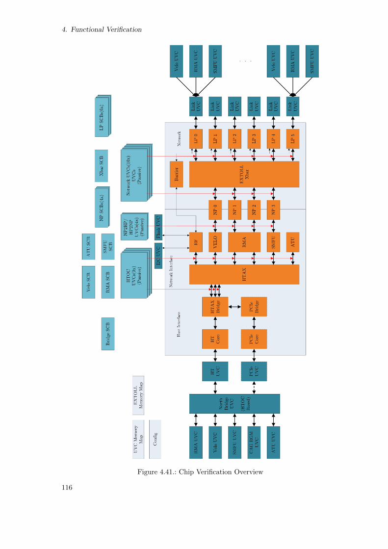
4. Functional Verification
Figure 4.41.: Chip Verification Overview
116

4.2. EXTOLL Functional Verification
Figure 4.42.: EXTOLL traffic directions
transactions from the needed interfaces. The LP scoreboards are connected to the link
UVCs and network UVCs connected to LP crossbar interfaces. The crossbar scoreboard is
connected to the network UVCs. The same way the other scoreboards for the other units
are connected.
When a transaction is sent to the DUV, it is monitored by the interface UVC and
forwarded to the first scoreboard. When this transaction passes the interface to the next
unit its sampled by the UVC monitoring this interface. This transaction is forwarded to two
scoreboards. The scoreboard for the unit which sends the transaction uses the transaction
to compare it with the expected ones. The scoreboard for the unit which receives the
transaction calculates the expected response transactions for this transaction. Following
this scheme, a transaction sent from one external interface to another is completely covered
by scoreboards during its whole lifetime, as all units are covered by a scoreboard. Therefore,
it can be checked that the transaction is processed correctly in the DUV.
All UVCs and scoreboards used so far to monitor and check the UVC were reused from
the unit TBs without any modifications to the original code. Only the UVM configuration
mechanism was used to disable the active parts of the UVCs. This was only possible because
during the implementation of the UVCs it was payed attention to separate the generation
and the monitoring of the DUV’s stimulus. Also, the scoreboards were implemented as real
passive components which receive its data for the DUV only by standard UVM interfaces.
4.2.5.2. Stimulus Generation
For a complete verification TB, also the stimulus for the DUV must be provided. For
EXTOLL two main generators can be distinguished. The one which creates stimulus from
the host, and another one which creates the stimulus from the link. This stimulus can be
further differentiated as shown in figure 4.42. There is traffic from the host targeting the
same host. This traffic uses the network crossbar for an internal loop back. Then there is
traffic from the host to a link and the other way round. In all these traffic patterns the
functional units of the network interfaced are involved. Consequently, the traffic must be
initiated by a valid unit transaction. This can be done by reusing the module UVC for
these units. In traffic from a link to another link only the LP and the network crossbar are
117
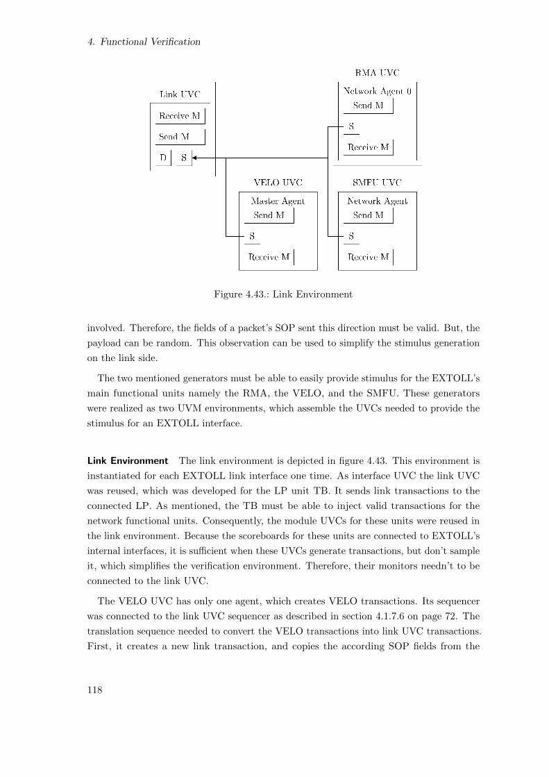
4. Functional Verification
Figure 4.43.: Link Environment
involved. Therefore, the fields of a packet’s SOP sent this direction must be valid. But, the
payload can be random. This observation can be used to simplify the stimulus generation
on the link side.
The two mentioned generators must be able to easily provide stimulus for the EXTOLL’s
main functional units namely the RMA, the VELO, and the SMFU. These generators
were realized as two UVM environments, which assemble the UVCs needed to provide the
stimulus for an EXTOLL interface.
Link Environment The link environment is depicted in figure 4.43. This environment is
instantiated for each EXTOLL link interface one time. As interface UVC the link UVC
was reused, which was developed for the LP unit TB. It sends link transactions to the
connected LP. As mentioned, the TB must be able to inject valid transactions for the
network functional units. Consequently, the module UVCs for these units were reused in
the link environment. Because the scoreboards for these units are connected to EXTOLL’s
internal interfaces, it is sufficient when these UVCs generate transactions, but don’t sample
it, which simplifies the verification environment. Therefore, their monitors needn’t to be
connected to the link UVC.
The VELO UVC has only one agent, which creates VELO transactions. Its sequencer
was connected to the link UVC sequencer as described in section 4.1.7.6 on page 72. The
translation sequence needed to convert the VELO transactions into link UVC transactions.
First, it creates a new link transaction, and copies the according SOP fields from the
118
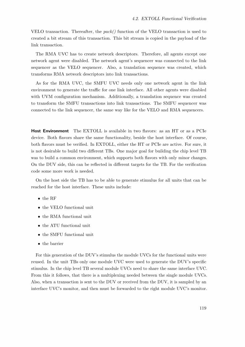
4.2. EXTOLL Functional Verification
VELO transaction. Thereafter, the pack() function of the VELO transaction is used to
created a bit stream of this transaction. This bit stream is copied in the payload of the
link transaction.
The RMA UVC has to create network descriptors. Therefore, all agents except one
network agent were disabled. The network agent’s sequencer was connected to the link
sequencer as the VELO sequencer. Also, a translation sequence was created, which
transforms RMA network descriptors into link transactions.
As for the RMA UVC, the SMFU UVC needs only one network agent in the link
environment to generate the traffic for one link interface. All other agents were disabled
with UVM configuration mechanism. Additionally, a translation sequence was created
to transform the SMFU transactions into link transactions. The SMFU sequencer was
connected to the link sequencer, the same way like for the VELO and RMA sequencers.
Host Environment The EXTOLL is available in two flavors: as an HT or as a PCIe
device. Both flavors share the same functionality, beside the host interface. Of course,
both flavors must be verified. In EXTOLL, either the HT or PCIe are active. For sure, it
is not desirable to build two different TBs. One major goal for building the chip level TB
was to build a common environment, which supports both flavors with only minor changes.
On the DUV side, this can be reflected in different targets for the TB. For the verification
code some more work is needed.
On the host side the TB has to be able to generate stimulus for all units that can be
reached for the host interface. These units include:
• the RF
• the VELO functional unit
• the RMA functional unit
• the ATU functional unit
• the SMFU functional unit
• the barrier
For this generation of the DUV’s stimulus the module UVCs for the functional units were
reused. In the unit TBs only one module UVC were used to generate the DUV’s specific
stimulus. In the chip level TB several module UVCs need to share the same interface UVC.
From this it follows, that there is a multiplexing needed between the single module UVCs.
Also, when a transaction is sent to the DUV or received from the DUV, it is sampled by an
interface UVC’s monitor, and then must be forwarded to the right module UVC’s monitor.
119
4. Functional Verification
Figure 4.44.: North Bridge UVC
North Bridge UVC To be able to support both EXTOLL flavors and to do the needed
multiplexing between the module UVCs, the so-called north bridge UVC was introduced
to the chip level TB. It is an intermediate layer between the module and interface UVCs
in the host environment.
All units of the EXTOLL’s network interface are connected to the HTAX. That’s why,
for their module TBs translation sequences from the module UVC transactions to HTOC
transactions were written to connect the module UVCs via the HTOC interface UVC to
the DUV. Because these sequences were already available, the decision was made to reuse
them in the chip level TB. This also had the consequence to use HTOC transactions for the
north bridge UVC. It had the advantage, that for the interface UVCs only one translation
sequence and monitor must be created to connect them to the upper levels, instead of
using a single one for each module UVC.
The north bridge UVC as an intermediate layer, also makes it possible to exchange the
host interface of the DUV with only minor changes to the TB. To change the interface,
another interface UVC must be used. As well as interface specific translation sequences
and monitors, which transform HTOC transactions into the specific interface transactions
and the other way round. All other parts of the host environment stay the same. These
translations were implemented for HT and PCIe. They are like the actual interface UVC
instances guarded by defines in the TB. To use a specific interface UVC a target sets either
CAG USE HT or CAG USE PCIE in the target specific build script.
The north bridge UVC is depicted in figure 4.44. It has three sequencers. One for each
VC(posted, non posted, and response) of the host interface. Beside the sequencers, it also
has two monitors. One for the stimulus sent to the DUV, and one for the transactions
sent by the DUV. The sequencers and monitors are connected via UVC layering to the
corresponding sequencers and monitors of the interface UVC.
When a north bridge monitor receives a transaction it needs to determine the module
UVC to which the transaction has to be forwarded. For read and write transactions
therefore a memory map is used. All functional units of EXTOLL can be identified by
120
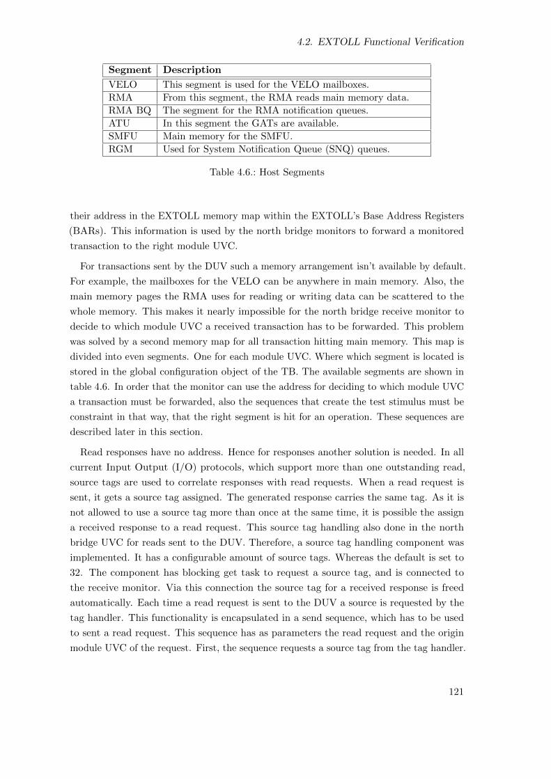
4.2. EXTOLL Functional Verification
Segment Description
VELO This segment is used for the VELO mailboxes.
RMA From this segment, the RMA reads main memory data.
RMA BQ The segment for the RMA notification queues.
ATU In this segment the GATs are available.
SMFU Main memory for the SMFU.
RGM Used for System Notification Queue (SNQ) queues.
Table 4.6.: Host Segments
their address in the EXTOLL memory map within the EXTOLL’s Base Address Registers
(BARs). This information is used by the north bridge monitors to forward a monitored
transaction to the right module UVC.
For transactions sent by the DUV such a memory arrangement isn’t available by default.
For example, the mailboxes for the VELO can be anywhere in main memory. Also, the
main memory pages the RMA uses for reading or writing data can be scattered to the
whole memory. This makes it nearly impossible for the north bridge receive monitor to
decide to which module UVC a received transaction has to be forwarded. This problem
was solved by a second memory map for all transaction hitting main memory. This map is
divided into even segments. One for each module UVC. Where which segment is located is
stored in the global configuration object of the TB. The available segments are shown in
table 4.6. In order that the monitor can use the address for deciding to which module UVC
a transaction must be forwarded, also the sequences that create the test stimulus must be
constraint in that way, that the right segment is hit for an operation. These sequences are
described later in this section.
Read responses have no address. Hence for responses another solution is needed. In all
current Input Output (I/O) protocols, which support more than one outstanding read,
source tags are used to correlate responses with read requests. When a read request is
sent, it gets a source tag assigned. The generated response carries the same tag. As it is
not allowed to use a source tag more than once at the same time, it is possible the assign
a received response to a read request. This source tag handling also done in the north
bridge UVC for reads sent to the DUV. Therefore, a source tag handling component was
implemented. It has a configurable amount of source tags. Whereas the default is set to
32. The component has blocking get task to request a source tag, and is connected to
the receive monitor. Via this connection the source tag for a received response is freed
automatically. Each time a read request is sent to the DUV a source is requested by the
tag handler. This functionality is encapsulated in a send sequence, which has to be used
to sent a read request. This sequence has as parameters the read request and the origin
module UVC of the request. First, the sequence requests a source tag from the tag handler.
121
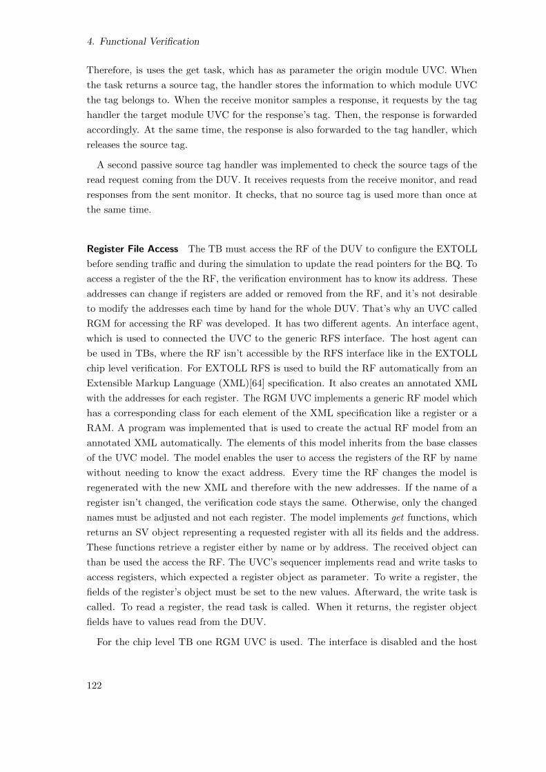
4. Functional Verification
Therefore, is uses the get task, which has as parameter the origin module UVC. When
the task returns a source tag, the handler stores the information to which module UVC
the tag belongs to. When the receive monitor samples a response, it requests by the tag
handler the target module UVC for the response’s tag. Then, the response is forwarded
accordingly. At the same time, the response is also forwarded to the tag handler, which
releases the source tag.
A second passive source tag handler was implemented to check the source tags of the
read request coming from the DUV. It receives requests from the receive monitor, and read
responses from the sent monitor. It checks, that no source tag is used more than once at
the same time.
Register File Access The TB must access the RF of the DUV to configure the EXTOLL
before sending traffic and during the simulation to update the read pointers for the BQ. To
access a register of the the RF, the verification environment has to know its address. These
addresses can change if registers are added or removed from the RF, and it’s not desirable
to modify the addresses each time by hand for the whole DUV. That’s why an UVC called
RGM for accessing the RF was developed. It has two different agents. An interface agent,
which is used to connected the UVC to the generic RFS interface. The host agent can
be used in TBs, where the RF isn’t accessible by the RFS interface like in the EXTOLL
chip level verification. For EXTOLL RFS is used to build the RF automatically from an
Extensible Markup Language (XML)[64] specification. It also creates an annotated XML
with the addresses for each register. The RGM UVC implements a generic RF model which
has a corresponding class for each element of the XML specification like a register or a
RAM. A program was implemented that is used to create the actual RF model from an
annotated XML automatically. The elements of this model inherits from the base classes
of the UVC model. The model enables the user to access the registers of the RF by name
without needing to know the exact address. Every time the RF changes the model is
regenerated with the new XML and therefore with the new addresses. If the name of a
register isn’t changed, the verification code stays the same. Otherwise, only the changed
names must be adjusted and not each register. The model implements get functions, which
returns an SV object representing a requested register with all its fields and the address.
These functions retrieve a register either by name or by address. The received object can
than be used the access the RF. The UVC’s sequencer implements read and write tasks to
access registers, which expected a register object as parameter. To write a register, the
fields of the register’s object must be set to the new values. Afterward, the write task is
called. To read a register, the read task is called. When it returns, the register object
fields have to values read from the DUV.
For the chip level TB one RGM UVC is used. The interface is disabled and the host
122

4.2. EXTOLL Functional Verification
Figure 4.45.: VELO Environment
agent is enabled. Its sequencer and monitors are connected to the north bridge UVC.
References to the host sequencer are used by other components to access its read and write
tasks and therefore the EXTOLL’s RF.
Functional Unit Environments As mentioned before, for the functional unit stimulus the
module UVCs were reused. These UVCs need some assistance from other UVCs to perform
its functionality. For example is the handling of the ring buffers which are used for the
VELO’s mailboxes done by the BQ UVC. The VELO UVC receives only the transaction
which is written to a ring buffer slot from the BQ UVC without only knowledge about
the ring buffer itself. To improve the clarity of the TB source code, it was partitioned
for the host environment. For each functional unit an own sub environment was created.
Therefore there are three environments:
• the VELO environment
• the RMA environment
• the SMFU environment
VELO Environment The VELO host environment is shown in figure 4.45 on the previous
page. It creates all stimulus, that is needed for the verification of the VELO. Beside
creating VELO messages, it also handles the BQ and the does the read pointer update
for the mailboxes. It includes instances of the VELO, WCB, and BQ UVCs. The VELO
UVC generates VELO transactions for the host interface. As the VELO uses a WCB
123

4. Functional Verification
instance to assemble the received VELO messages from the host system, a WCB UVC is
connected to the VELO UVC. This way, the WCB sequences for splitting messages, as
well as the translation sequences from VELO to WCB transactions could be reused. The
WCB sequencer is connected to the posted sequencer of the north bridge UVC.
The north bridge sent monitor samples the VELO messages sent to the DUV. It is
connected to WCB monitor, which is then connected to the VELO requester monitor.
The monitors translate step by step from HTOC transactions over WCB transactions
into VELO transactions. They were all reused from the previously developed module
TBs. The VELO’s completer monitor is connected to the VELO scoreboard. On host
side the scoreboard is connected to the external interface and not to a internal interface
monitor. This solution was chosen, because the UVCs were needed for the stimulus
generation, and were already available. To sample the internal VELO interface to the
HTAX interface a complete second set of VELO, WCB, and BQ UVCs would be needed.
As the VELO transaction isn’t further modified on its way to the host interface, and is
easily distinguishable on this interface from other traffic by its address, the decision was
made to connect the VELO scoreboard to the external interface monitors. It also doesn’t
reduce it observability of errors, as the HTAX bridge is covered by an own scoreboard,
which detects errors in the bridge.
As the VELO’s mailboxes are constraint to be in the VELO segment of the verification
memory map, the north bridge receive monitor forwards received transactions targeting a
VELO mailbox to the BQ UVC of the VELO environment. After checking the received
transaction, that is targets the right ring buffer address, it is forwarded to the completer
monitor. The monitor translates the transaction into a VELO transaction. It is then sent
to the scoreboard, as the requester transactions.
The BQ implements ring buffers for storing data in main memory. These ring buffers
needn’t to be in continuous memory regions and can be distributed across the whole main
memory. This distribution is hidden from the functional units by the BQ. The BQ has
to know were the single segments of ring buffer are in main memory. This information is
stored in a data structure called descriptor queue. There, for each segment its base address
and size is stored. The BQ loads the descriptor for the next segment, when the write
pointer reach the end of a segment. When the TB creates a new VELO mailbox, it has
also to creates the descriptors for the ring buffer segments randomly and stores them in the
descriptor queue handler of the BQ UVC. The TB needs to response to BQ main memory
reads to its descriptor queues. Therefore, the BQ responder component was developed.
The descriptor queues are constraint to be in the VELO segment of the verification memory
map. Consequently, the north bridge receive monitor is able to forward these reads to the
BQ responder. The responder uses the read address to find the right descriptor queue, reads
the next segment from the BQ UVC’s descriptor handler and creates a read response. The
124
4.2. EXTOLL Functional Verification
read response data is assembled out of the data for the requested segment, and equates to
the memory layout for descriptor queue entry as specified in the BQ specification[31]. The
response is the sent to the DUV via the north bridge UVC. Of course, the BQ responder
checks, that the next requested segment is the next expected one.
A mailbox has a read and a write pointer. The write pointer indicates the next free
slot, and is handled in hardware. The read pointer points to the next slot in which the
next messages is expected by the software. It is incremented each time the software
has processed a message. The hardware has to know, when the mailbox is full to avoid
overwriting messages, that weren’t read before. Therefore, the hardware has a copy of
the software’s read pointer. The hardware isn’t allowed to write to the next slot, when
write pointer + 1 = read pointer. To avoid, that a mailbox gets full, the software has to
update the hardware’s read pointer with its current read pointer. As in the verification
environment no software is available, another method has to be applied for the update to
imitate the software’s behavior. Actually, the verification environment has to keep a read
pointer for each mailbox. It’s incremented for each received VELO message and has to
be written to hardware’s read pointer. Therefore, a read pointer update component was
introduced. It has a read pointer for each mailbox and receives each VELO message from
the DUV from the BQ UVC’s monitor. Then the read pointer for the according mailbox is
incremented. Afterward, a random timeout is started. When the timeout is reached, the
current read pointer is written to the RF of the DUV with the help of the RGM UVC. If
in the mean time another message was received, then the read pointer to be written has a
larger difference than one from the previous one. The difference between the previous and
the next read pointer can be controlled by the constraint for the timeout. If the timeout
is small, also read pointer difference is small. A large timeout leads to full mailbox. The
default constraint has three ranges for the timeout. A small one, a middle one, and a large
one.
RMA Environment The RMA host environment is shown in figure 4.46 on the following
page. First, this environment has to create RMA software descriptors. Second, the RMA
uses the ATU for NLA to physical address translation. Therefore, it has to respond
to translation requests. Third, the environment has to respond to read requests from
main memory. Fourth, the notifications from the RMA for completed descriptors are
stored in ring buffers. The environment has to provide the infrastructure to handle these.
Consequently, the host environment has instances of the RMA, ATU, and BQ UVC, which
are reused from the module TBs.
For the RMA UVC, the request agent and the memory responder are enabled. The
request agent’s sequencer, which generates software descriptors is connected to the posted
sequencer of the north bridge UVC. The request agent’s monitor is connected to send
125
4. Functional Verification
Figure 4.46.: RMA Environment
monitor of north bridge UVC. The translation sequence and the translating monitor are
reused from the module TB. The memory responder receives read requests from the north
bridge’s receive monitor and uses the responses sequencer for sending the responses. The
ATU UVC uses its memory agent for responding to GAT read requests from the DUV. It
is also connected to the north bridge UVC’s receive monitor and response sequencer. The
BQ UVC is used to receive the notifications, which are stored in ring buffers.
For the BQ read pointer update the same read pointer update component as for the
VELO environment is used. As well as the BQ responder component to respond to
descriptor queue reads.
SMFU Environment The SMFU forwards local write and read requests to remote nodes.
Therefore, the SMFU environment(see figure 4.47 on the next page) has to create requests,
which targets the SMFU’s BAR address. It has also to generate responses for read requests
received from the DUV. Thus, the environment uses an instance of the SMFU UVC, with
its host agent enabled. As the UVC sends traffic on all VCs of the host interface, the host
agent’s sequencer is connected to the posted, non posted and response sequencers of the
north bridge UVC. A special send sequence was implemented for the host sequencer, which
forwards a generated transaction to the right north bridge sequencer according to its VC.
The host agent’s send and receive monitors are connected to the send and receive monitors
126
4.2. EXTOLL Functional Verification
Figure 4.47.: SMFU Environment
of the north bridge UVC. The SMFU UVC implements an automatic response sequence
for received read requests, which was also used in the SMFU environment.
The translation sequences from SMFU transactions into HTOC transactions as well as
the translating monitors were reused from the SMFU’s module TB.
Debug Interfaces EXTOLL has two debug interfaces. The I2C interface is used two
access the EXTOLL’s RF independently from the host interface. The flash interface
connects a flash chip, in which patches to modify the RF’s default values can be stored.
The RF reads these values and writes them to the according registers during the reset
phase of EXTOLL. To verify the I2C access and the patch behavior, an I2C and a flash
UVC were connected to the DUV. The I2C UVC was an own development, whereas the
flash UVC was used from the Cadence VIP Catalog[65].
As the patching process from the flash memory needs some simulation time and has to
take place in the reset sequence, the patching is verified in a special test of the TB. This
reduces the run time for all other tests without any reduction of the overall test coverage.
EXTOLL Initialization Before the TB can sent random traffic to the EXTOLL it has
to be initialized. For example the routing table of the network crossbar has to be set, in
order that the crossbar forwards any packets to other destinations than the same node.
Therefore, a set of initialization sequences for each functional block was written for a
better modularity of the initialization process. Additionally, a main initialization sequence
was implemented, that executes the other sequences step by step. As the initialization
sequences has to be executed by each test, this improved the clarity of the tests and hides
the complexity from the test writer.
All the configuration settings, which are written during the initialization, are stored
127
4. Functional Verification
Fields Description random
Node ID The node ID of the DUV. *
Link Count The number of available links.
VELO segment base address The base address of the VELO segment
Table 4.7.: Configuration Parameters
in the RF of the DUV. Therefore, all sub initialization sequences uses the RGM UVC
instance of the TB to access the RF.
The TB has a couple of global configuration parameters. These parameters are used to
configure the TB when it is build, and during the simulation for constraining the stimulus.
It is randomized before the TB gets build. Table 4.7 lists all available parameters.
Following sub initialization sequences were implemented:
Host Interface The host interface initialization sequence configures the host interface. For
HT, it starts with a cold reset. Afterward, the HT link is configured as by the Basic
Input Output System (BIOS). It starts with reading the capabilities of the device,
followed by the setting the link configuration registers of the device to the desired
link width and link frequency. They can be set in the global configuration object of
the TB. After a warm reset is done and the link has finished its low level training
sequence, the initialization sequence does the device enumeration to set the BARs.
For PCIe, the PCIe UVC does the initialization completely automatically without
any user involvement. As for HT, this includes setting the PCIe configuration space
registers like the BARs. When the initialization is finished, the UVC triggers an
event. Consequently, for PCIe the host interface initialization sequence just waits for
this event before it finishes itself.
Whether the HT or PCIe initialization is done, is controlled by the CAG USE HT
and CAG USE HT defines, which are also used the select the host interface for a
DUV target.
Node ID This sequence writes the own node ID of the DUV into its RF. The node ID’s
value can be set in the global configuration object of the TB.
HTAX bridge The HTAX bridge uses an interval mapper to decide to which port of the
HTAX a request from the host interface has to be sent. After the reset the interval
mapper is disabled and all requests are sent to the RF by default. In order to
sent requests to the other functional units than RF, the interval mapper needs to
be configured. The address ranges for each interval are configured in the global
configuration object.
This sequence writes the address ranges for each interval into the RF and enables
128
4.2. EXTOLL Functional Verification
the interval mapper.
Routing Table The network crossbar uses a table based routing[31]. Its routing has to
be initialized in order that the crossbar knows to which port a packet has to be
forwarded. The TB reuses the routing table component of the network crossbar TB
to handle the routing table entries. The entries of this table are randomized in the
end of elaboration phase of the TB. The initialization sequence writes the entries of
the routing table component into the routing tables of the network crossbar.
RMA The RMA uses PDIDs for a basic access control to other VPIDs. These are stored
in a VPID table in the RF. The RMA UVC implements a VPID handler to make the
PDIDs available to the TB. This sequence writes the entries of the VPID handler
into the RF. It also sets the host MTU of the RMA, initializes the BQ for the RMA,
and enables the NPs connected to the RMA.
ATU This sequence writes the base addresses of the ATU’s GATs. The ATU UVC stores
these addresses in its GAT handler, from where the GATs are available to the TB.
The sequence also enables the ATU in the RF.
VELO As the RMA, the VELO uses PDIDs as a security mechanism. These PDIDs are
handled by the VPID handler component of the VELO UVC, and are randomized in
the end of elaboration phase of the TB. The initialization sequence writes the PDIDs
into DUV, and enables the BQ for the VELO, and the NP connected to the VELO.
SMFU This sequence writes the address offsets, which are needed for the address mapping
to remote nodes by the SMFU. Additionally, it enables the NP connected to the
SMFU.
Sequence Library In the chip level TB, the sequencers of the module UVCs can’t create
complete random transactions. As mentioned before, the TB uses an own memory map on
the host interface to be able to separate the transactions sent to main memory. Therefore,
all transactions sent to the DUV have to be constraint in order that resulting transactions
targeting main memory hit the right segment.
Additionally, the target node of transactions has to be constraint as well. For traffic
from a link to the host, the node ID of the DUV has to be used. In the routing table not
all entries initialized with valid entries, as in the simulation it lasts a long time to write all
210 entries. Measurements have shown, that the simulation needs about two hours to write
a complete routing table. For a random constraint verification it is sufficient to initialize
only a small amount of entries, if they are chosen randomly. The verification coverage is
reached by running the simulation over and over again with different seeds for the random
constraint solver. Therefore, all packets sent to the network crossbar must be constraint to
use a destination node, which has a valid routing table entry.
129

4. Functional Verification
Figure 4.48.: Virtual Sequencer References
To create a valid input stimulus, a set of sequences was implemented. These sequences
ensure with the help of different constraints, that the generated transactions fulfill the
mentioned constraints. As they have to access different components of the TB like the
routing table, they are executed on the virtual sequencer of the TB.
As mentioned in section 4.1.7.5 on page 72, each TB has one virtual sequencer, which
controls all other sequencers in the TB by starting transactions or sequences on UVC
sequencers. Consequently, the virtual sequencer for the chip level TB(see figure 4.48) has
references to the module UVC sequencers of the host environment, which includes the
VELO, RMA, and SMFU sequencers. For the initialization a reference to the host interface
sequencer is available. To sent stimulus to the link interfaces, there are references to each
module UVC’s sequencers for each link environment. Beside these sequencer references, the
virtual sequencer needs access to different handler components of the UVCs. This includes
references to the routing table to receive a valid target node, to the VPID tables for the
RMA and VELO to access the PDIDs, and to the GAT of the RMA UVC to register
new translations. Additionally, a reference to the global configuration object of the TB is
available. It is used to access the address ranges of the memory segments.
1 class SEQUENCENAME extends uvm sequence ;
2
3 rand TRANSACTION TYPE t r ;
4
5 b i t [ 6 3 : 0 ] l ower addre s s ;
6 b i t [ 6 3 : 0 ] upper address ;
7
8 constraint addre s s c {9 t r . address i n s i d e { [ l ower addre s s : upper address ] } ;
10 }11
12 ‘ u vm ob j e c t u t i l s (SEQUENCENAME)
13 ‘ uvm dec l a r e p sequence r ( v i r t u a l s e qu en c e r )
14
130

4.2. EXTOLL Functional Verification
15 function void pre randomize ( ) ;
16 i f ( t r == nu l l )
17 t r = TRANSACTION TYPE: : type id : : c r e a t e ( ” t r ” ) ;
18
19 l ower addre s s = p sequencer . c f g . segments [RMA] . l ower addre s s ;
20 upper address = p sequencer . c f g . segments [RMA] . upper address ;
21 endfunction : pre randomize
22
23 task body ( ) ;
24 TRANSACTION TYPE m tr ;
25
26 t r . t a rge t node = p sequencer . r t . get random node ( ) ;
27
28 ‘uvm create on (m tr , p sequencer . rma l i nk s eq r [ l i n k ] )
29 m tr . copy ( t r ) ;
30 ‘uvm send (m tr )
31 endtask : body
32
33 endclass
Listing 4.2: Sequence Structure
All sequences of the chip level TB’s sequence library have the same structure, which
is depicted in listing 4.2 on the preceding page. This structure allows the sequence user
a complete control over the generated stimulus on the one hand, on the other hand it
automates as much as possible. First, there is a field(line 2) of the transaction type the
sequence sends, which is declared random. This way, the field gets randomize when the
sequence is started with the ‘uvm do macro. Default constraints in the sequence ensure,
that the created transaction follows the global TB’s constraints. The pre randomize()(line
15) function is called by the simulator prior to the randomize() function. It first creates a
new transaction object, as no transaction object is created by default when the sequence
object is created. Then, default values are loaded from the global configuration object. In
this example the lower and upper address for a main memory segment. The constraint
in line 8 constraints the address of the transaction with the help of the addresses set in
pre randomize(). As mentioned above, not all routing table entries are set in the routing
table. Thus, the destination node of the a transaction can’t be randomized freely. Therefore,
a function called get random node() was implemented for the routing table component,
which returns a random existing node ID. This function is called in line 26 within the body
task(). This task is executed by UVM after the randomization of the sequence. In line
28 and following lines, the random created transaction is forwarded to the module UVC
sequencer on which the transaction should be sent.
The following sequences are written for the TB:
Link to Link This sequence sends EXTOLL packets from on link to another without hitting
131
4. Functional Verification
a functional unit. In its body task the routing table’s get random node() function to
receive a random target node, which is not local host.
VELO Host It sends one random VELO message from the host to the VELO requester.
The target node is set using the routing table’s get random node() function.
VELO Link This sequence sends one VELO message from a random link to VELO com-
pleter. The link to be used can be constraint with the link id field. The target node
ID is set to the node ID of the DUV. It also sets the right PDID for the message’s
VPID with the help of the VELO’s VPID table component.
RMA Host The RMA host sequence sends one RMA software descriptor from the host to
the RMA. A constraint ensures that the read address for acr:put requests is inside the
RMA’s memory segment. If the randomized software descriptor indicates the use of
a NLA via a set transation enable fields, the sequence adds random page translations
to the ATU’s GAT for the affected pages of the request. The target node is set using
the routing table’s get random node() function.
RMA Link This sequence sends a single RMA descriptor from a random link to the RMA.
Whether the descriptor is sent to the responder or the completer is randomized by
its target field. Depending on the target, the descriptor’s command is constraint
accordingly. For responder descriptors to gets. For completer descriptors to puts
and get responses. As for the RMA sequence the addresses of the network descriptor
are constraint to hit the RMA’s main memory segment, and also necessary page
translations are added to the ATU’s GAT. The target node ID is constraint to the
DUV’s node ID.
SMFU Host The SMFU host sequence sends a single SMFU request from the host to the
SMFU. The address of the sent request is constraint to hit the BAR of the SMFU.
That a valid target node ID is hit by the resulting network target, is reached by
constraining the part of the address with encodes the target node ID accordingly.
SMFU Link This sequence sends a SMFU request from a random link to the SMFU. The
address of the request is constraint to hit the SMFU’s main memory segment. The
target node ID is constraint to the DUV’s node ID.
Tests After the TB was in place, the last step for the chip level verification environment
was to create meaningful tests. These tests were built to verify, that all units of EXTOLL
function with each other as intended in the specification. The strategy for building the
tests was as follows. First, a small simple test was written for the bring up of the TB.
After the TB successfully compiled, the first stimulus was sent to the device. Thereby,
each functional unit was tested after each other. The tests started with sending only a
couple of transactions to see, if the TB works as intend. Then, the amount of transactions
132

4.2. EXTOLL Functional Verification
was increased. After the test for the single functional units worked, a test was written in
which all units are used. All tests use the sequences from the TB’s sequence library for the
generation of the stimulus.
Following tests were created:
Simple Test This test sends 100 transactions for each functional unit from the host to the
link and the other way round. It not intended to run in regression. It is a short test
to check that there is nothing broken after a major change to the DUV or the TB.
VELO It is used to only test the VELO. It sends 5000 VELO messages from the host into
the network, and 5000 VELO messages from the links the to host.
RMA It is used to only test the RMA. It sends 5000 RMA descriptors from the host into
the network, and 5000 RMA descriptors from the links the to host.
SMFU It is used to only test the SMFU. It sends 5000 SMFU requests from the host into
the network, and 5000 SMFU requests from the links the to host.
Link to Link The link to link test sends traffic from one link to another one without hitting
the network interface. Combined, it sent 5000 network packets.
Random Traffic This test is intended to stress EXTOLL. It sends random traffic for all
functional units from the host into the network, and from the links to the host
together with traffic which only crosses the network crossbar. In for each functional
unit and direction 5000 packets are send.
4.2.6. Regression Analysis
For a complete verification, it isn’t enough to build TBs, which are able to generate random
stimulus and run each test once. This way, it isn’t possible to verify all features of the
design sufficiently. Therefore, a regression is needed. A regression is the process of running
all available tests repeatedly each time with a different seed value for the random constraint
solver. This leads to a different stimulus for each run of the same test. As normally
several hundreds to thousands of different runs are needed to reach coverage closure, it
isn’t practical to start each run by hand. Therefore, regression tools are used to automate
the process of launching the tests.
Such a regression tool is the Enterprise Manager from Cadence Design Systems[66],
which was used for the verification of EXTOLL. It manages to execution of the single test
runs, and integrates a tool for the coverage analysis. A file format called VSIF is used to
describe a single regression run. This description includes which tests for a TB have to be
executed in a regression run, and how often. For each TB, a shell script has to be specified,
which is used to the start the TB. Therefore, the run scripts described in section 4.2.3.2 on
133

4. Functional Verification
Figure 4.49.: Regression HTML Report
page 93 were used.
The goal for the EXTOLL regression was to have completely automated regression with
the following features:
• As there are daily changes to both the RTL and TB source code, regression should
be started each evening.
• Each regression run has to use always the latest source code.
• Automatic status notification via email.
• Creation of an up-to-date coverage report.
All these goals were realized with a set of scripts. The main script is started every
evening by a cron job. It first updates the source code of the RTL and the TBs from the
SVN. Then the regression is started. Therefore, the eManager is started with a VSIF,
which is located in the SVN. For the eManager a script was written, that creates a summary
of the regression in a text file when the eManager finishes. This file includes for each test
if it succeeded or not, and if not, the error reported by the TB is added to the report
file. Afterward, this reported is sent by email to all module owners. Another script parses
the report for errors, and adds tickets to the bug tracking system. This way, no bugs are
missed, and get documented for a further risk analysis.
During the regression, the eManager also collects coverage data. This collected data
is stored a a database for a further analysis. With each regression run, the accumulated
134
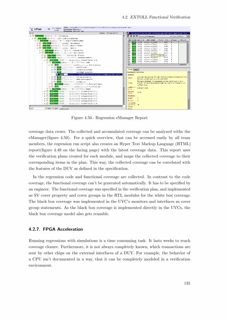
4.2. EXTOLL Functional Verification
Figure 4.50.: Regression eManager Report
coverage data crows. The collected and accumulated coverage can be analyzed withe the
eManager(figure 4.50). For a quick overview, that can be accessed easily by all team
members, the regression run script also creates an Hyper Text Markup Language (HTML)
report(figure 4.49 on the facing page) with the latest coverage data. This report uses
the verification plans created for each module, and maps the collected coverage to their
corresponding items in the plan. This way, the collected coverage can be correlated with
the features of the DUV as defined in the specification.
In the regression code and functional coverage are collected. In contrast to the code
coverage, the functional coverage can’t be generated automatically. It has to be specified by
an engineer. The functional coverage was specified in the verification plan, and implemented
as SV cover property and cover groups in the RTL modules for the white box coverage.
The black box coverage was implemented in the UVC’s monitors and interfaces as cover
group statements. As the black box coverage is implemented directly in the UVCs, the
black box coverage model also gets reusable.
4.2.7. FPGA Acceleration
Running regressions with simulations is a time consuming task. It lasts weeks to reach
coverage closure. Furthermore, it is not always completely known, which transactions are
sent by other chips on the external interfaces of a DUV. For example, the behavior of
a CPU isn’t documented in a way, that it can be completely modeled in a verification
environment.
135
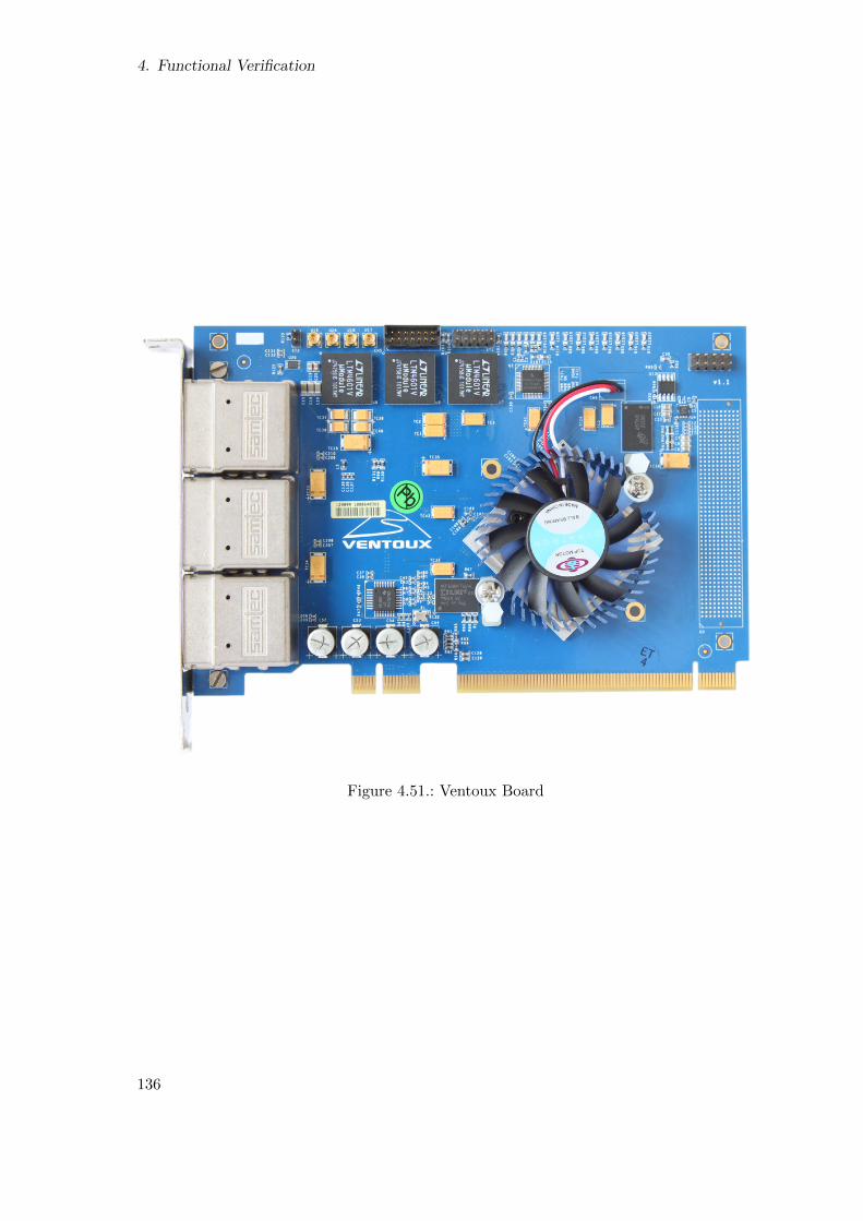
4. Functional Verification
Figure 4.51.: Ventoux Board
136

4.2. EXTOLL Functional Verification
Therefore, the functional verification of EXTOLL was combined with an emulation of
the design in an FPGA. This way, it was possible to test the design in its final environment.
As EXTOLL can be used with HT or PCIe as host interface, two FPGA boards were
developed at the CAG. Both, uses a Virtex 6 FPGA[67] from Xilinx. The board named
Ventoux(figure 4.51) has a HT interface and provides six network links. The Galibier board
uses PCIe and provides four links.
During the implementation of the EXTOLL’s RTL, it was payed attention to have
a very generic RTL implementation. All technology specific components like RAMs or
Phase Looked Loops (PLLs) were wrapped in generic modules with standardized interfaces.
Therefore, the main RTL can easily mapped to different technologies as FPGAs or ASICs
by exchanging the wrappers with technology specific implementations. Of course, larger
blocks like the host interface or the serializers for the network links needs more attention
for changing the target technology.
After the mapping of the DUV to the FPGA boards was finished, test programs were
developed by the CAG to sent data over the network. First, the functional units were
tested using an internal loop back in the network crossbar. Afterward, the amount of nodes
in the network was increased step by step. By running the test programs, errors could be
identified either by the reception of wrong data, or by not responding hardware. Then,
the bug was isolated with the goal of finding the smallest possible use case, which triggers
the error. Therefore, a lot of debug registers were added to all units of EXTOLL, which
are accessible by the RF. These debug registers include for example counters for packets
or flow control credits, as well as the state registers of important FSMs. With the help
of these debug registers the unit causing the error and the condition which leads to the
error can be identified. This approach can encircle the error, but can’t point directly to
the logic function with the error.
Indeed, there are logic analyzers available witch are integrated in the FPGAs, but they
aren’t capable to monitor all registers in the design at the same time. Instead, the engineer
has to specify the registers of interest, and build a special bit file for the FPGA including
the analyzer watching these registers. As only subset of registers can be monitored this way,
many bit files must be built to identify the erroneous logic function. Also, this integration
influences the timing of the FPGA’s logic, which makes it hard to meet the needed timing.
Therefore, in addition to the functional verification flow, a combination of functional
verification and FPGA testing was used. As mentioned, an error only can be encircled in
an FPGA. But, the knowledge gained from this analysis can be used to build test, which
triggers the error. As random constraint TBs are used for the verification, it isn’t needed
to exactly model the stimulus, which leads to an error. For example, when the analysis
shows, that the error is triggered by small messages on a high network load, then the test
137
4. Functional Verification
is constraint only to sent a lot of small messages with small gaps between each other. As
in the simulation all registers are accessible, and can be viewed in a waveform viewer, it is
possible to find and fix the logic error more easily.
With this additional methodology, it is possible to identify errors in the design much
master, than in simulation. In simulation, the DUV runs in terms of kilo Hertz. In contrast,
the FPGA platforms operates with 200 MHz. The lack of observability of errors in the
FPGA is eliminated by building a specific random test in a verification TB.
The FPGA platform makes it also possible to build and test the needed software for the
design, before the ASIC is ready. Consequently, the software hardware interaction can be
tested extensively in an early design phase, which helps to improve the software hardware
interface. In addition, the software is also ready and tested for the bring up of the ASIC,
when it returns from the fab.
4.2.8. Conclusion
This section described a complete and efficient verification methodology for a large chip
design. After describing the features of the EXTOLL design, the main external and internal
interfaces as well as functional units were identified. These findings lead to a library of
verification IPs, which were implemented using UVM. By the consequent reuse of the
developed UVCs, the code needed for the verification environments could be reduced. This
was also possible, because of the clean design of EXTOLL with clearly defined functionality
for each unit without spreading a functionality over different units, and a set of standardized
internal interfaces.
The efficiency of the chosen verification approach was demonstrated with the implemen-
tation of the chip level TB for EXTOLL. For this TB most verification code was reused
from the unit TBs. There the analysis of the design in the beginning of the verification
process helped in building compact, reusable verification IPs which were then used in the
different TBs.
With the FPGA acceleration approach, a verification methodology was introduced,
which combines the advantages of FPGA prototyping with the ones of a simulation based
verification. There, the FPGA is used to speedup the detection of bugs, whereas the
simulation based verification is used to fix the bug with the help of its observability and
checking capabilities. This combined approach reduced the time needed to eliminate the
most critical bugs in the design, and showed several hard to find ones.
Furthermore, a completely automated regression suite was developed. This suite is
started each evening and checks regularly the latest RTL code. With an automated error
reporting by email and the use of the bug tracking tool trac, the errors found in the
138
4.3. Verification Tools
regression get documented, which helps in fixing all errors as well as in an analysis of
the main causes for errors. This analysis can help in avoiding these errors in a following
project.
4.3. Verification Tools
As mentioned in the introduction, one requirement for a state of the art verification
environment is its efficiency. The engineers have to focus on the features and architecture
of a design. The verification tends to be a ”necessary evil”. Therefore, many work was done
to develop verification methodologies based on simulation or formal verification to improve
the efficiency of the verification process. All these methodologies have in common, that
the automation grade of building new verification environments is very limited. However,
a high automation grade reduces the probability of making errors in the implementation
phase of a chip. For example, the synthesis of an RTL implementation into a gate level net
list is completely automated today. In contrast, a verification environment needs to be
build manually from the specification. This process needs a good methodology like the one
presented in the last sections to avoid errors. There are tools available for simulation or the
coverage analysis after a regression. But, tools to assist in building these environments are
not available, beside advanced editors. Many tasks in building verification environments
must be repeated in this process. To provide the engineer with more help in building a
TB, the following section suggests creating tools to improve the efficiency of building TBs.
4.3.1. Testbench Creator
Creating a new TB is a time consuming task. For each TB always the same tasks must be
fulfilled. These task are shown in the following:
1. Create the directory structure for the TB. As described in section 4.2.3.1 on page 87
a sophisticated directory structure helps in using the TB.
2. Create the basic files for the TB. This includes:
• The run script to launch the TB.
• The compile file to load the source files and configure the simulator.
• The top module, which includes the verification code, instantiates the DUV,
and creates the clocks and resets for the DUV.
• The TB file, were the UVCs are instantiated.
• The virtual sequencer, which controls the other UVC sequencers.
139

4. Functional Verification
• A basic test to start the environment.
3. Instantiate and connect the DUV to the SV interfaces of the UVCs.
4. Instantiate and configure the UVCs needed for the TB. This includes adding the SV
interfaces for the UVC DUV communication.
5. Create a scoreboard for the DUV.
6. Connect the UVCs with the SV interface instances, connected the monitors with the
scoreboard, and connect the interface UVCs with the module UVCs as described in
section 4.1.7.6 on page 72.
7. Create the tests for the TB.
For the steps one and two, a Perl script was already created for the EXTOLL’s verification.
It expects as argument the name of the TB to be created. It then creates a new sub
directory with the name of the TB, followed by the building the directory structure of the
TB. Afterward, the files described in step two are created. When the script finishes, the
newly created TB can be started immediately. Then, the verification engineer has to do
steps three to seven, which is the main work. But, this scripts makes it more easier to
start a new TB.
This script is the first step for a comprehensive tool for creating a TB. The goal is to
build a tool, which enables the user to create a new TB with a graphical interface. The
requirements for such a tool are:
• A parser, that supports to read UVCs and detects their sequencers, monitors, drivers,
sequences, and interfaces.
• A GUI to connect the DUV with the interfaces required for the communication with
UVCs.
• A GUI to connect these interfaces with the UVCs.
• A GUI to connect UVCs as described in section 4.1.7.6 on page 72.
• An automatic creation of the virtual sequencer with connections to all sequencers in
the verification environment.
• Support for grouping UVCs in bigger environments, like in the chip verification of
EXTOLL, in order the structure the verification environment.
• The ability to allow the user to insert own code to specific UVM phases like build, or
connect.
• A GUI to create new tests with the ability to allow test overrides of verification
components.
140
4.3. Verification Tools
• Support for graphical test sequence generation.
• A code generator for the verification environment built.
141

5. Conclusion
The functional complexity of hardware designs grows steadily. This growth is driven by
shrinking node sizes of the process technology. At the same time, the costs for manufacturing
an ASIC increases. For a research institute it gets more difficult to build a new innovative
hardware design. As they have limited resources, there is the pressure to have a working
ASIC by the first submission. Usually, a re-spin is not affordable by a research institute.
Therefore, an efficient design and verification methodology is needed to avoid a re-spin.
The goal of this thesis was to developed a new efficient network protocol, a barrier
synchronization for an unified network, and a complete and comprehensive verification
methodology, that can be realized with limited manpower.
The first contribution of this thesis is a new efficient, flexible, and reliable network
protocol for an HPC interconnection network. It uses a data granularity of 64 Bits. Thus,
it can be easily adapted to different data widths for the internal data path of the EXTOLL
network. This was reached by using 64 Bits wide cells, which are either used as control
cells for the framing and link management, or as data cells for the network packet data
transport. The overhead for the framing of a packet was minimized to 16 Bytes. Therefore,
the network protocol reaches an efficiency of 91%. Thereby, it is one of the most efficient
network protocols for HPC.
The network protocol efficiency is reached without losing the reliability of the protocol.
In fact, the reliability of the new protocol was improved by using strong CRCs for the
protection of the control cells and the packet’s data. By the use of a CRC in each control
cell, it was possible to protect the routing information of each packet. Thus, it can
be guaranteed, that only valid routing information is passed to the network crossbar.
Consequently, in the case of an error, packets are not forwarded to a wrong destination
node or block the network anymore. The retransmission protocol was also improved to be
more fault tolerant by the use of timeouts. Also, the credits used for the flow control are
now part of the retransmission.
The second contribution is an innovative hardware barrier synchronization directly
integrated into the EXTOLL interconnection network. Its efficiency is reached by using
special control cells for the transport of the barrier messages. The barrier logic is realized
in an own module inside the network layer. Instead of using the network crossbar for the
143
5. Conclusion
message routing, it is done by the barrier module itself. Therefore, the barrier module is
connected to all LPs of EXTOLL. The distributing of barrier messages to the right LPs
is done by the barrier module. Thus, a barrier message passes the barrier module in 5
clock cycles, in contrast to 15, which would be needed, if the network crossbar was used.
Beside, the barrier synchronization, the barrier logic was extended to support a new global
network interrupt, which is able to trigger an interrupt on all nodes, or a subset of nodes,
exactly at the same time. The barrier logic was implemented in Verilog, and verified with
the formal verification. In addition, the barrier was tested in an FPGA implementation.
There, it was shown, that the implementation needs 1,2us to synchronize a network of 9
nodes.
In addition, a complete and comprehensive verification methodology for a large ASIC
was developed and implemented. By using a structured methodology, it was possible
to realize the functional verification of the design with very limited resources. The first
step in the verification process was the analysis of the design. Therefore, the main units
were identified, and verification plans for each unit were created. The verification plans
summarized the features and functionality of the units. Furthermore, checks and coverage
items were extracted from these for the later use in the verification.
A key aspect for the successful verification was the consequent reuse of verification code
across the TBs. Before the TBs were created, the main interfaces used between the units
were identified. For these interfaces, interface UVCs were created to generate and check
the stimulus of theses interfaces. Thereafter, the TBs for the main units were built by
using the interface UVCs. Additional module UVCs were used to generate stimulus and
check behavior specific for each unit. For each TB, also a scoreboard was implemented.
Furthermore, multiple tests were created to verify specific behaviors of the units, and the
functional coverage was implemented to track the verification process.
After all unit TBs were available a system level TB was created to verify the connectivity
and interaction of the units. Therefore, the verification code implemented for the unit TBs
was reused, which enabled it to build this TB very fast.
To help to structure the verification, a new directory structure for all TBs was developed.
This structure contributed to be able to reuse verification code across the TBs, and helped
the users of the TBs to use them more easily.
Furthermore, a completely automated regression suite was build. It is started on a daily
basis, and helps to find new bugs shortly after changes made to the RTL code. After a
regression run is finished, a report is generated to summarize the success of each test run.
Failing tests are added by the regression suite to a bug tracking tool for further investigation
of the responsible unit owners, and to understand what kind of bugs were found in order
to avoid them next time. The regression suite also collects coverage data. This data is
144
merged into a single coverage database. It allows the tracking of the verification process,
and makes the verification process more predicable. When all coverage items, which are
defined in the verification plans, are met then is the DUV ready for tape out from the
perspective of the functional verification.
Beside the simulation based functional verification, also FPGAs were used to accelerate
the verification process. On the one hand, a simulation is very slow in comparison to
an FPGA implementation. On the other hand, bugs can be analyzed more easily in a
simulation, as all signals are accessible in a waveform viewer. Therefore, an innovative
hybrid approach was developed for the verification, which uses the benefits of both solutions.
The DUV is mapped to an FPGA. There the design is executed in its real environment.
If a hardware failure occurs, the workload pattern, which lead to this failure, is analyzed
and minimized to a very small set of traffic. This pattern is then used to create a random
constraint test for the DUV in the simulation to trigger the failure. Thereafter, the failure
is analyzed and corrected.
Due to the verification efforts, it was possible to install a 9 node test cluster with
EXTOLL as interconnection network at the CAG. This cluster is used to develop the
software environment needed for EXTOLL. Currently, the interconnection network functions
as intended without any known hardware bugs. As the verification for the FPGA target
was successful, it is foreseeable, that the verification of the ASIC is successful as well, which
makes a re-spin unnecessary.
145

A. SystemVerilog Assertions
A.1. Introduction
SV[68] is programming language for hardware design and hardware verification. To
assist the verification engineer with the checking of a DUV, it introduces assertions. An
assertion specifies the behavior of a system, and does a claim about the expected behavior.
Consequently, they are primarily used to validate the behavior of a design. In addition,
assertions can be used to provide functional coverage and generate input stimulus for formal
validation. An assertion specifies the behavior of a design by describing the relationship of
the design’s signals in time. For example, it is not allowed to shift data into a FIFO if
the FIFO is full. An assertion which checks this behavior would look like the following
example:
assert ( ! ( f u l l && s h i f t i n ) ) ;
Listing A.1: Immediate Assertion
If the DUV behaves correctly this assertion will evaluate to true. Otherwise, a failure of
the assertion will be reported during simulation.
SV assertions are used for checking the DUV in a simulation based verification. In
simulation they aren’t capable to provide an input stimulus for the DUV. The stimulus
must be created by a verification environment as described in chapter 4 on page 45. In a
formal verification environment, they are used for both creating the stimulus and checking
the behavior. Assertions for the input signals of a DUV create the stimulus. They other
assertions check the DUV behavior.
A.2. Assertion Types
SV distinguishes between two kinds of assertions: concurrent and immediate assertions.
Immediate assertions follow simulation event semantics for their execution and are executed
like a statement in a procedural block. Immediate assertions are primarily intended to be
used with simulation.
147
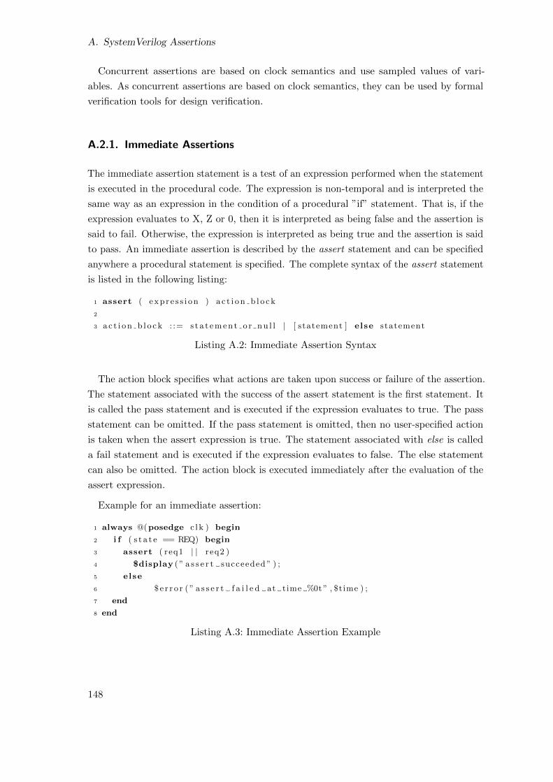
A. SystemVerilog Assertions
Concurrent assertions are based on clock semantics and use sampled values of vari-
ables. As concurrent assertions are based on clock semantics, they can be used by formal
verification tools for design verification.
A.2.1. Immediate Assertions
The immediate assertion statement is a test of an expression performed when the statement
is executed in the procedural code. The expression is non-temporal and is interpreted the
same way as an expression in the condition of a procedural ”if” statement. That is, if the
expression evaluates to X, Z or 0, then it is interpreted as being false and the assertion is
said to fail. Otherwise, the expression is interpreted as being true and the assertion is said
to pass. An immediate assertion is described by the assert statement and can be specified
anywhere a procedural statement is specified. The complete syntax of the assert statement
is listed in the following listing:
1 assert ( exp r e s s i on ) a c t i on b l o ck
2
3 a c t i on b l o ck : := s t a t emen t o r nu l l | [ statement ] else statement
Listing A.2: Immediate Assertion Syntax
The action block specifies what actions are taken upon success or failure of the assertion.
The statement associated with the success of the assert statement is the first statement. It
is called the pass statement and is executed if the expression evaluates to true. The pass
statement can be omitted. If the pass statement is omitted, then no user-specified action
is taken when the assert expression is true. The statement associated with else is called
a fail statement and is executed if the expression evaluates to false. The else statement
can also be omitted. The action block is executed immediately after the evaluation of the
assert expression.
Example for an immediate assertion:
1 always @(posedge c l k ) begin
2 i f ( s t a t e == REQ) begin
3 assert ( req1 | | req2 )
4 $display ( ” a s s e r t succeeded ” ) ;
5 else
6 $e r r o r ( ” a s s e r t f a i l e d at time %0t ” , $time ) ;
7 end
8 end
Listing A.3: Immediate Assertion Example
148
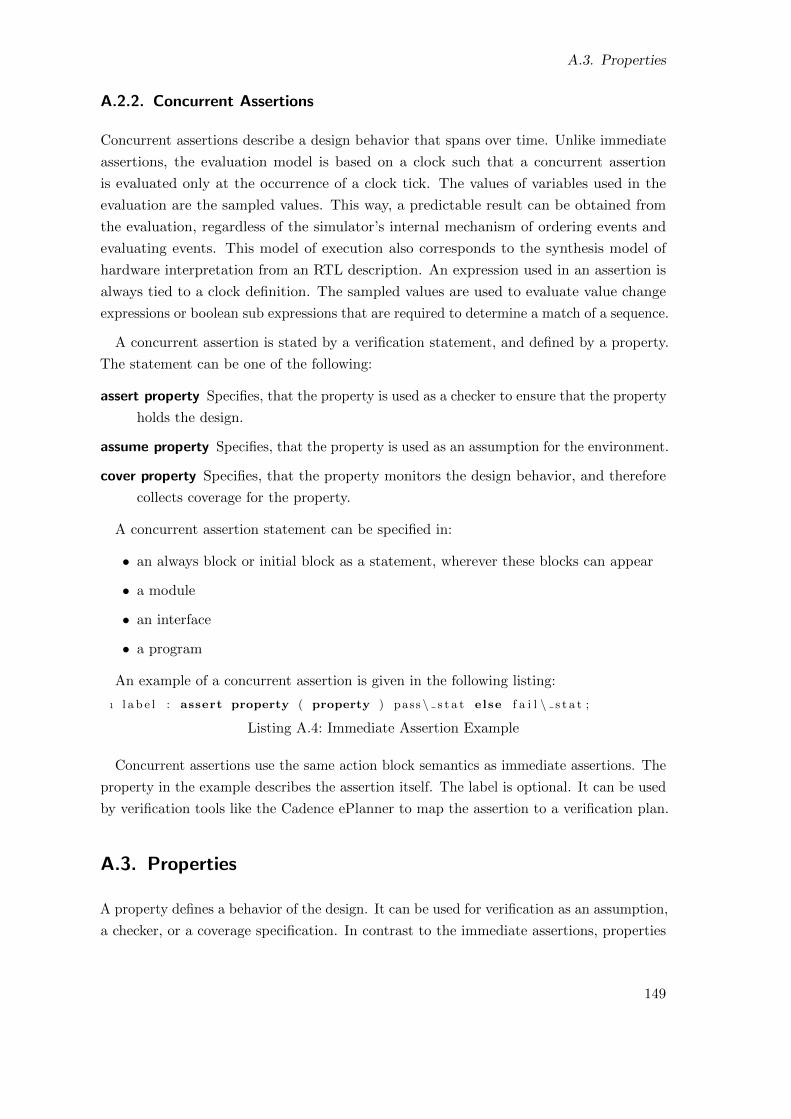
A.3. Properties
A.2.2. Concurrent Assertions
Concurrent assertions describe a design behavior that spans over time. Unlike immediate
assertions, the evaluation model is based on a clock such that a concurrent assertion
is evaluated only at the occurrence of a clock tick. The values of variables used in the
evaluation are the sampled values. This way, a predictable result can be obtained from
the evaluation, regardless of the simulator’s internal mechanism of ordering events and
evaluating events. This model of execution also corresponds to the synthesis model of
hardware interpretation from an RTL description. An expression used in an assertion is
always tied to a clock definition. The sampled values are used to evaluate value change
expressions or boolean sub expressions that are required to determine a match of a sequence.
A concurrent assertion is stated by a verification statement, and defined by a property.
The statement can be one of the following:
assert property Specifies, that the property is used as a checker to ensure that the property
holds the design.
assume property Specifies, that the property is used as an assumption for the environment.
cover property Specifies, that the property monitors the design behavior, and therefore
collects coverage for the property.
A concurrent assertion statement can be specified in:
• an always block or initial block as a statement, wherever these blocks can appear
• a module
• an interface
• a program
An example of a concurrent assertion is given in the following listing:
1 l a b e l : assert property ( property ) pass \ s t a t else f a i l \ s t a t ;
Listing A.4: Immediate Assertion Example
Concurrent assertions use the same action block semantics as immediate assertions. The
property in the example describes the assertion itself. The label is optional. It can be used
by verification tools like the Cadence ePlanner to map the assertion to a verification plan.
A.3. Properties
A property defines a behavior of the design. It can be used for verification as an assumption,
a checker, or a coverage specification. In contrast to the immediate assertions, properties
149
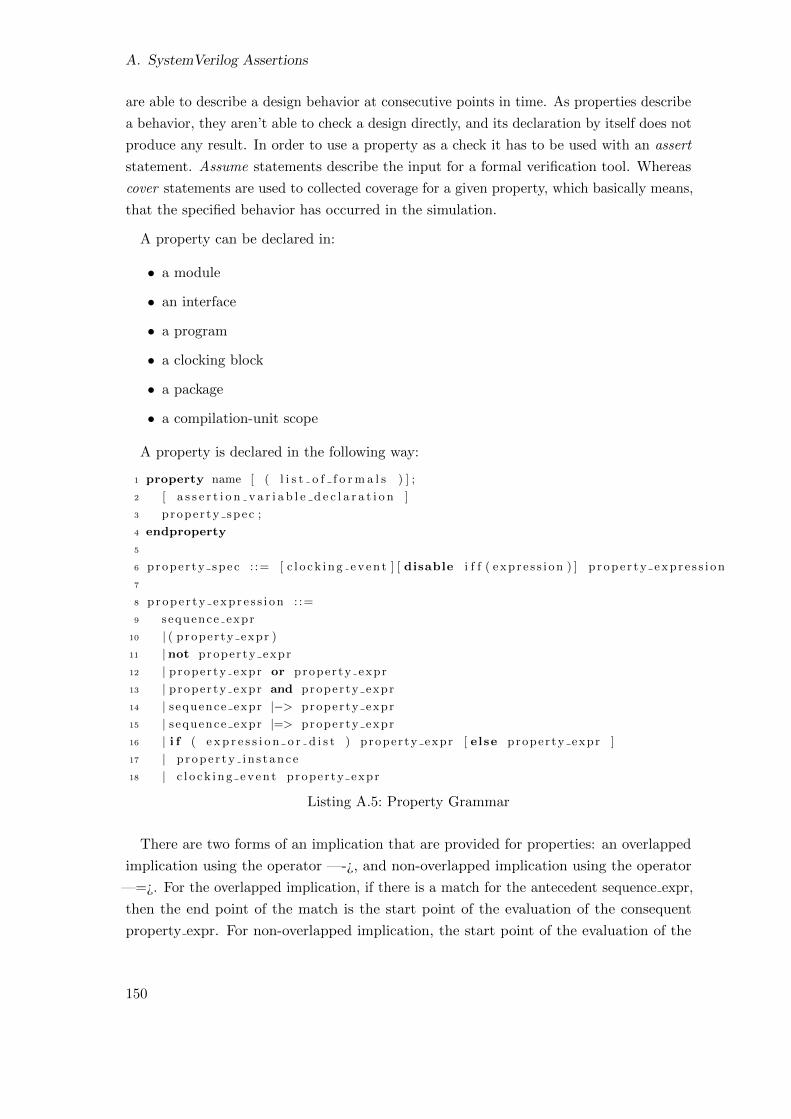
A. SystemVerilog Assertions
are able to describe a design behavior at consecutive points in time. As properties describe
a behavior, they aren’t able to check a design directly, and its declaration by itself does not
produce any result. In order to use a property as a check it has to be used with an assert
statement. Assume statements describe the input for a formal verification tool. Whereas
cover statements are used to collected coverage for a given property, which basically means,
that the specified behavior has occurred in the simulation.
A property can be declared in:
• a module
• an interface
• a program
• a clocking block
• a package
• a compilation-unit scope
A property is declared in the following way:
1 property name [ ( l i s t o f f o rm a l s ) ] ;
2 [ a s s e r t i o n v a r i a b l e d e c l a r a t i o n ]
3 prope r ty spec ;
4 endproperty
5
6 prope r ty spec : := [ c l o ck i ng ev en t ] [ disable i f f ( exp r e s s i on ) ] p r ope r ty exp r e s s i on
7
8 prope r ty exp r e s s i on : :=
9 sequence expr
10 | ( proper ty expr )
11 | not proper ty expr
12 | proper ty expr or proper ty expr
13 | proper ty expr and proper ty expr
14 | sequence expr |−> proper ty expr
15 | sequence expr |=> proper ty expr
16 | i f ( e x p r e s s i o n o r d i s t ) proper ty expr [ else proper ty expr ]
17 | prope r ty i n s t anc e
18 | c l o ck i ng ev en t proper ty expr
Listing A.5: Property Grammar
There are two forms of an implication that are provided for properties: an overlapped
implication using the operator —-¿, and non-overlapped implication using the operator
—=¿. For the overlapped implication, if there is a match for the antecedent sequence expr,
then the end point of the match is the start point of the evaluation of the consequent
property expr. For non-overlapped implication, the start point of the evaluation of the
150
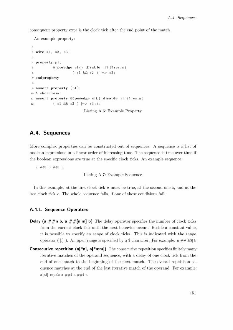
A.4. Sequences
consequent property expr is the clock tick after the end point of the match.
An example property:
1
2 wire s1 , s2 , s3 ;
3
4 property p1 ;
5 @(posedge c l k ) disable i f f ( ! r e s n )
6 ( s1 && s2 ) |=> s3 ;
7 endproperty
8
9 assert property ( p1 ) ;
10 A short form :
11 assert property (@(posedge c l k ) disable i f f ( ! r e s n )
12 ( s1 && s2 ) |=> s3 ; ) ;
Listing A.6: Example Property
A.4. Sequences
More complex properties can be constructed out of sequences. A sequence is a list of
boolean expressions in a linear order of increasing time. The sequence is true over time if
the boolean expressions are true at the specific clock ticks. An example sequence:
a ##1 b ##1 c
Listing A.7: Example Sequence
In this example, at the first clock tick a must be true, at the second one b, and at the
last clock tick c. The whole sequence fails, if one of these conditions fail.
A.4.1. Sequence Operators
Delay (a ##n b, a ##[n:m] b) The delay operator specifies the number of clock ticks
from the current clock tick until the next behavior occurs. Beside a constant value,
it is possible to specify an range of clock ticks. This is indicated with the range
operator ( [:] ). An open range is specified by a $ character. For example: a ##[3:$] b
Consecutive repetition (a[*n], a[*n:m]) The consecutive repetition specifies finitely many
iterative matches of the operand sequence, with a delay of one clock tick from the
end of one match to the beginning of the next match. The overall repetition se-
quence matches at the end of the last iterative match of the operand. For example:
a[∗3] equals a ##1 a ##1 a
151
A. SystemVerilog Assertions
Goto repetition (a[-¿n], a[-¿n:m]) The goto repetition specifies finitely many iterative
matches of the operand boolean expression, with a delay of one or more clock ticks
from one match of the operand to the next successive match and no match of the
operand strictly in between. The overall repetition sequence matches at the last
iterative match of the operand. For example: a[−>1] equals (!a)[∗0:\$] \#\#1 a
Non-consecutive repetition (a[=n], a[=n:m]) The non-consecutive repetition specifies
finitely many iterative matches of the operand boolean expression, with a delay of
one or more clock ticks from one match of the operand to the next successive match
and no match of the operand strictly in between. The overall repetition sequence
matches at or after the last iterative match of the operand, but before any later
match of the operand. For example: a[=1] equals (!a)[∗0:\$] ##1 a ##1 (!a)[∗0:\$]
And Operator (a and b) The and operator matches, if both sequences match, and the
start time of both is the same. The end time can be different.
Or operator (a or b) The or operator matches, if one of the sequences match.
Intersect operator (AND with length restriction) (a intersect b) The intersect opera-
tor matches, if both sequences match and the start and and time is the same.
First match operator (first match( a )) The first match operator matches only the first
of possibly multiple matches for an evaluation attempt of its operand sequence.
Throughout operator (a throughout b) The throughout operator matches, if a is true
during the whole match of b. It is an abbreviation for: (expr)[∗0:\$] intersect b
Within operator (a within b) The within operator matches, if b matches and a is true at
some point of this interval.
A.5. Local Variables
SV supports the declaration of local variables inside properties and sequences. They are
used to pass data for one stage in a sequential expression to a later stage. The following
data types are supported as local variables:
bit, byte, int, integer, logic, reg, time, packed struct, class, arrays of supported types
An example for local variables:
1 property p i p e l i n e ;
2 b i t [ 6 3 : 0 ] x ;
3 @(posedge c l k ) disable i f f ( ! r e s n )
4 ( va l id , x = data in ) |=> ##5 ( data out == (x+1)) ;
5 endproperty
152
A.6. Assertion Writing Guidelines
Listing A.8: Local Variable Example
A.6. Assertion Writing Guidelines
The SV assertion language sub set is a powerful language for writing assertions. It allows to
describe very complex design behavior by using properties and sequences. The drawback of
this complexity is, that is possible to write properties, which can slow down the simulation a
lot. To avoid common mistakes in writing assertions, [69] gives some advice for maximizing
the assertion performance. The following paragraphs will show some of these advices with
the help of bad examples and how they can be avoided.
Minimize the number of attempts Properties with an enabling condition, that is true a
lot of times, slows down the simulator a lot.
1 property bad ;
2 @(posedge c l k ) disable i f f ( ! r e s n )
3 va l i d && enable |−> a ve ry l ong s equence ;
4 endproperty : bad
Listing A.9: Slow Assertion
Use instead:
1 property good ;
2 @(posedge c l k ) disable i f f ( ! r e s n )
3 $rose ( va l i d ) && enable |−> a ve ry l ong s equence ;
4 endproperty : good
Listing A.10: Improved Assertion
Minimize false starts Try to start sequences or property enabling conditions with a
condition that is rarely true.
1 sequence bad ;
2 a ##1 b ##2 c ;
3 endsequence : bad
Listing A.11: Improved Assertion
If b is rarely true and a is true very often, a better solution is the following one:
1 sequence good ;
2 ( $past ( a ) && b) ##2 c ;
3 endsequence : good
Listing A.12: Improved Assertion
153
A. SystemVerilog Assertions
Cadence NCSim Profiler SystemVerilog Assertions Examples
A.7. System Functions
Assertions are commonly used to evaluate specific characteristics of a design. Therefore
some system functions are available to simplify this evaluation. The following functions
are available:
$onehot(〈expression〉) returns true if only one bit of the expression is high
$onehot0(〈expression〉) returns true if at most one bit of the expression is high
$isunkown(〈expression〉) returns true if any bit of the expression is X or Z. This is
equivalent to 〈expression〉 ===′ bx.
$countounes(〈expression〉) returns the number of 1s in the expression.
A.8. SVA Examples
1 sequence l e ng th o f p a ck e t ;
2 ##[1:32] ##1 any eox ;
3 endsequence : l e n g th o f p a ck e t
4
5 property l e g a l d a t a v a l i d ;
6 @(posedge c l k ) disable i f f ( ! r e s e t n )
7 ( da t a va l i d && $rose ( any sox ) ) |−>8 da ta va l i d throughout l e ng th o f p a ck e t ;
9 endproperty : l e g a l d a t a v a l i d
10 da ta va l i d : assert property ( l e g a l d a t a v a l i d ) ;
11
12 unknown valid : assert property ( @(posedge c l k ) disable i f f ( ! r e s n )
13 va l i d |−> $isunknown ( s igna l name )
14 ) ;
15
16 unknown : assert property ( @(posedge c l k ) disable i f f ( ! r e s n )
17 ! $isunknown ( s igna l name )
18 ) ;
Listing A.13: Assertion
154
Bibliography
[1] (). Top500, [Online]. Available: http://www.top500.org (visited on 12/06/2012).
[2] (). Hpl benchmark, [Online]. Available: http://icl.cs.utk.edu/hpl (visited on
12/06/2012).
[3] P. Luszczek, J. J. Dongarra, D. Koester, R. Rabenseifner, B. Lucas, J. Kepner,
J. McCalpin, D. Bailey, and D. Takahash, “Introduction to the HPC Challenge
Benchmark Suite”, Lawrence Berkeley National Laboratory, Tech. Rep., 2005.
[4] IEEE, IEEE Std 802.3-2008 Part 3: Carrier sense multiple access with Collision
Detection (CSMA/CD) Access Method and Physical Layer Specifications, December.
2008, vol. 2008, isbn: 9730738157.
[5] Infiniband Trade Association, Architecture Specification Volume 1 Release 1.2.1,
November. 2007, vol. 1.
[6] N. R. Adiga, M. a. Blumrich, D. Chen, P. Coteus, a. Gara, M. E. Giampapa, P.
Heidelberger, S. Singh, B. D. Steinmacher-Burow, T. Takken, M. Tsao, and P.
Vranas, “Blue Gene/L torus interconnection network”, IBM Journal of Research
and Development, vol. 49, no. 2.3, pp. 265–276, Mar. 2005, issn: 0018-8646. doi:
10.1147/rd.492.0265. [Online]. Available: http://ieeexplore.ieee.org/
lpdocs/epic03/wrapper.htm?arnumber=5388784.
[7] R. Alverson, D. Roweth, and L. Kaplan, “The Gemini System Interconnect”, in
18th IEEE Symposium on High Performance Interconnects, IEEE, 2010, pp. 83–
87, isbn: 9781424485475. doi: 10.1109/HOTI.2010.23. [Online]. Available: http:
//ieeexplore.ieee.org/xpls/abs\_all.jsp?arnumber=5577317.
[8] J. Duato, S. Yalmanchili, and L. Ni, Interconnection Networks an Engineering
Approach, M. Fayad, Ed. Matt Loeb, 1997.
[9] Information Sciences Institute University of Southern California, Internet security
glossary (ietf rfc 791): internet protocol, The Internet Society, 1981.
[10] ——, Internet security glossary (ietf rfc 793): transmission control protocol, The
Internet Society, 1981.
[11] Infiniband Trade Association, “Infiniband Architecture Specifiaction Volume 2 Release
1.3”, Tech. Rep., 2012.
155

Bibliography
[12] Mellanox Technologies, “FDR InfiniBand is Here”, Tech. Rep., 2011.
[13] A. Gara, M. a. Blumrich, D. Chen, G. L.-T. Chiu, P. Coteus, M. E. Giampapa, R. a.
Haring, P. Heidelberger, D. Hoenicke, G. V. Kopcsay, T. a. Liebsch, M. Ohmacht, B. D.
Steinmacher-Burow, T. Takken, and P. Vranas, “Overview of the Blue Gene/L system
architecture”, IBM Journal of Research and Development, vol. 49, no. 2.3, pp. 195–212,
Mar. 2005, issn: 0018-8646. doi: 10.1147/rd.492.0195. [Online]. Available: http:
//ieeexplore.ieee.org/lpdocs/epic03/wrapper.htm?arnumber=5388794.
[14] “Overview of the ibm blue gene/p project”, IBM Journal of Research and Develop-
ment, vol. 52, no. 1.2, pp. 199 –220, Jan. 2008, issn: 0018-8646. doi: 10.1147/rd.
521.0199.
[15] R. Haring, M. Ohmacht, T. Fox, M. K. Gschwind, D. L. Satterfield, K. Sugavanam,
P. W. Coteus, P. Heidelberger, M. A. Blumrich, R. W. Wisniewski, A. Gara, G. L.-T.
Chiu, P. A. Boyle, N. H. Christ, and C. Kim, “The IBM Blue Gene/Q Compute
Chip”, Micro, IEEE, vol. 32, no. 2, pp. 48–60, 2012.
[16] D. Chen, N. A. Eisley, P. Heidelberger, R. M. Senger, Y. Sugawara, S. Kumar, V.
Salapura, D. L. Satterfield, B. Steinmacher-Burow, and J. J. Parker, “The IBM Blue
Gene/Q Interconnection Fabric”, Micro, IEEE, vol. 32, no. 1, pp. 32–43, 2012.
[17] D. Chen, J. J. Parker, N. a. Eisley, P. Heidelberger, R. M. Senger, Y. Sugawara,
S. Kumar, V. Salapura, D. L. Satterfield, and B. Steinmacher-Burow, “The IBM Blue
Gene/Q interconnection network and message unit”, Proceedings of 2011 International
Conference for High Performance Computing, Networking, Storage and Analysis
on - SC ’11, p. 1, 2011. doi: 10.1145/2063384.2063419. [Online]. Available:
http://dl.acm.org/citation.cfm?doid=2063384.2063419.
[18] M. Yokokawa, F. Shoji, A. Uno, M. Kurokawa, and T. Watanabe, “The K Computer”,
in Low Power Electronics and Design (ISLPED) 2011 International Symposium on,
2011, pp. 371–372, isbn: 9781612846606.
[19] Y. Ajima, Y. Takagi, T. Inoue, S. Hiramoto, and T. Shimizu, “The Tofu Interconnect”,
2011 IEEE 19th Annual Symposium on High Performance Interconnects, pp. 87–94,
Aug. 2011. doi: 10.1109/HOTI.2011.21. [Online]. Available: http://ieeexplore.
ieee.org/lpdocs/epic03/wrapper.htm?arnumber=6041538.
[20] T. Topology, I. N. Which, E. Cubic, T. Graph, A. Users, T. O. Run, M. Topology,
A. Applications, H. I. S. Article, D. The, O. F. U. I. Architecture, O. F. U. N.
Router, O. F. U. N. Interface, O. F. U. B. Interface, and P. E. Results, “The Tofu
interconnect”, pp. 21–31, 2012.
[21] X.-j. Yang, X.-K. Liao, K. Lu, Q.-f. Hu, J.-Q. Song, and J.-s. Su, “The TianHe-1A
Supercomputer: Its Hardware and Software”, Science And Technology, vol. 26, no.
2009, pp. 344–351, 2011. doi: 10.1007/s11390-011-1137-4.
156

Bibliography
[22] M. Xie, Y. Lu, L. Liu, H. Cao, and X. Yang, “Implementation and Evaluation of
Network Interface and Message Passing Services for TianHe-1A Supercomputer”,
2011 IEEE 19th Annual Symposium on High Performance Interconnects, pp. 78–86,
Aug. 2011. doi: 10.1109/HOTI.2011.20. [Online]. Available: http://ieeexplore.
ieee.org/lpdocs/epic03/wrapper.htm?arnumber=6041537.
[23] M. Xie, Y. Lu, K. Wang, L. Liu, H. Cao, and X. Yang, “Tianhe-1A Interconnect and
Message-Passing Services”, Micro, IEEE, vol. 32, no. 1, pp. 8–20, 2012.
[24] P. Koopman, “32-bit cyclic redundancy codes for Internet applications”, in Proceedings
International Conference on Dependable Systems and Networks, IEEE Comput.
Soc, 2002, pp. 459–468, isbn: 0-7695-1597-5. doi: 10.1109/DSN.2002.1028931.
[Online]. Available: http://ieeexplore.ieee.org/lpdocs/epic03/wrapper.htm?
arnumber=1028931.
[25] P. Koopman and T. Chakravarty, “Cyclic redundancy code (CRC) polynomial
selection for embedded networks”, International Conference on Dependable Systems
and Networks, 2004, pp. 145–154, 2004. doi: 10.1109/DSN.2004.1311885.
[26] F. Ueltzhoffer, “Design and Implementation of a Virtual Channel Based Low-Latency
Crossbar Switch”, Diploma Thesis, University of Mannheim, 2005.
[27] D. Slogsnat, “Tightly-Coupled and Fault-Tolerant Communication in Parallel Sys-
tems”, Phd. Thesis, University of Mannheim, 2008.
[28] A. X. Widmer and P. A. Franaszek, “A DC-Balanced, Partioned-Block, 8B/10B
Transmission Code”, IBM Journal of Research and Development, vol. 27, no. 5,
pp. 440 –451, 1983.
[29] H. Froning, “Architectural Improvements of Interconnection Network Interfaces”,
Phd. Thesis, University of Mannheim, 2007.
[30] M. Nussle, “Acceleration of the hardware - software interface of a communication
device for parallel systems”, Phd. Thesis, University of Mannheim, 2008.
[31] B. U. Geib, “Hardware Support for Efficient Packet Processing”, PhD thesis, Univer-
sity of Mannheim, 2012.
[32] ISO/IEC, Information technology - Open Systems Interconnection - Basis Reference
Model: The Basic Model (ISO/IEC 7498-1), 1983.
[33] H. Froning and H. Litz, “Efficient hardware support for the partitioned global address
space”, in Parallel & Distributed Processing, Workshops and Phd Forum (IPDPSW),
2010 IEEE International Symposium on, IEEE, 2010, pp. 1–6. [Online]. Available:
http://ieeexplore.ieee.org/xpls/abs\_all.jsp?arnumber=5470851.
157
Bibliography
[34] F. Petrini, D. J. Kerbyson, and S. Pakin, “The Case of the Missing Supercomputer
Performance: Achieving Optimal Performance on the 8,192 Processors of ASCI Q”,
in Supercomputing, 2003 ACM/IEEE Conference, 2003, isbn: 1581136951.
[35] H. F. Jordan, “A Special Purpose Architecture for Infinite Element Analysis”,
Institute for Computer Applications in Science and Engineering NASA Langley
Research Center, Hampton, Virginia, Tech. Rep., 1978.
[36] R. Sivaram, C. B. Stunkel, and D. K. Panda, “A reliable hardware barrier syn-
chronization scheme”, in Parallel Processing Symposium, 1997. [Online]. Available:
http://ieeexplore.ieee.org/xpls/abs\_all.jsp?arnumber=580908.
[37] J. Hill and D. Skillicorn, “Practical barrier synchronisation”, in Parallel and Dis-
tributed Processing, 1998. [Online]. Available: http://ieeexplore.ieee.org/xpls/
abs\_all.jsp?arnumber=647231.
[38] D. Panda, “Fast barrier synchronization in wormhole k-ary n-cube networks with
multidestination worms”, in Proceedings of the 1996 In- ternational Conference on
High-Performance Computer Architecture, 1996. [Online]. Available: http://www.
sciencedirect.com/science/article/pii/0167739X9500026O.
[39] H. Xu, P. K. McKinley, and L. M. Ni, “Efficient implementation of barrier synchro-
nization in wormhole-routed hypercube multicomputers”, in Proceedings of the 12th
International Conference on Distributed Computing Systems, 1992. [Online]. Available:
http://www.sciencedirect.com/science/article/pii/074373159290031H.
[40] E. D. Brooks, “The butterfly barrier”, International Journal of Parallel Programming,
vol. 15, no. 4, pp. 295–307, 1986.
[41] N. Burkhardt, “Fast Hardware Barrier Synchronisation for a Reliable Interconnection
Network”, Diploma Thesis, University of Mannheim, 2007.
[42] G. E. Moore. (). Moore’s law, [Online]. Available: http://en.wikipedia.org/wiki/
Moore’s_law (visited on 08/07/2012).
[43] F. Faggin, M. E. Hoff, S. Mazor, and M. Shima, “The History of the 4004”, Micro,
IEEE, 1996. [Online]. Available: http://ieeexplore.ieee.org/xpls/abs\_all.
jsp?arnumber=546561.
[44] S. Sawant, U. Desai, G. Shamanna, L. Sharma, M. Ranade, A. Agarwal, S. Dakshina-
murthy, and R. Narayanan, A 32nm Westmere-EX Xeon enterprise processor, 2011.
doi: 10.1109/ISSCC.2011.5746225.
[45] European Semiconductor Industry Association, Japan Electronics and Information
Technology Industries Association, Korea Semiconductor Industry Association, Tai-
wan Semiconductor Industry Association, and Semiconductor Industry Association,
158
Bibliography
“International Technology Roadmap for Semiconductors 2011 Edition”, Tech. Rep.,
2011.
[46] J. Bergeron, Writing testbenches: functional verification of HDL models. Kluwer
Academic Publishers, 2003, isbn: 0306476878.
[47] N. K. Shimbun, Poka-Yoke: Improving Product Quality by Preventing Defects. 1988.
[48] PCI SIG. (). PCI Express Base Specification, [Online]. Available: http://www.
pcisig.com/specifications/pciexpress/base3 (visited on 08/23/2012).
[49] Hypertransport Technology Consortium, HyperTransport(TM) I / O Link Specifica-
tion. 2008.
[50] N. Heaton. (). Maximizing Verification Effectiveness Using Metric-Driven Verification,
[Online]. Available: http://www.cadence.com/rl/Resources/white_papers/max_
metric_driven_ver_wp.pdf (visited on 09/03/2012).
[51] R. Bryant, “Binary decision diagrams and beyond: enabling technologies for formal ver-
ification”, Proceedings of IEEE International Conference on Computer Aided Design
(ICCAD), pp. 236–243, 1995. doi: 10.1109/ICCAD.1995.480018. [Online]. Available:
http://ieeexplore.ieee.org/lpdocs/epic03/wrapper.htm?arnumber=480018.
[52] E. M. Clarke, E. a. Emerson, and a. P. Sistla, “Automatic verification of finite-
state concurrent systems using temporal logic specifications”, ACM Transactions on
Programming Languages and Systems, vol. 8, no. 2, pp. 244–263, Apr. 1986, issn:
01640925. doi: 10.1145/5397.5399. [Online]. Available: http://portal.acm.org/
citation.cfm?doid=5397.5399.
[53] Accellera Organization, Inc. (). UVM World, [Online]. Available: http://www.
uvmworld.org (visited on 09/17/2012).
[54] H. Miller and T. Alsop, “UVM VIP-TSC Status”, in Design Automation Conference,
2010, 2010.
[55] S. Rosenberg and K. A. Meade, A Pratical Guide to Adopting the Universal Verifica-
tion Methodology (UVM). Cadence Design Systems, 2010.
[56] Accellera, “Universal Verification Methodology (UVM) 1.1 User’s Guide”, Tech. Rep.,
2011.
[57] E. Gamma, R. Helm, R. Johnson, and J. Vlissides, Design Patterns: Elements of
Reusable Object-Oriented Software. Addison-Wesley, 1994, p. 395.
[58] Open SystemC Initiative, “OSCI TLM-2.0 Language Reference Manual”, Tech. Rep.
July, 2009.
[59] H. Litz, “HyperTransport Advanced X-Bar (HTAX) Specification”, University of
Heidelberg, Tech. Rep., 2010.
159

Bibliography
[60] C. H. Leber, “Efficient Hardware for Low Latency Applications”, PhD thesis, Uni-
versity of Mannheim, 2012.
[61] A. Giese, B. Kalisch, and M. Nussle, “RMA2 Specification”.
[62] I. Cadence Design Systems, “Universal Verification Methodology (UVM) Introduc-
tion”, Tech. Rep. November, 2011.
[63] ——, “ICC User Guide”, Tech. Rep. May, 2012.
[64] World Wide Web Consortium. (). XML, [Online]. Available: http://www.w3.org/XML
(visited on 11/26/2012).
[65] I. Cadence Design Systems, “Cadence VIP Catalog”, Tech. Rep., 2011.
[66] ——, Incisive Management, 2005.
[67] Xilinx, “Virtex-6 Family Overview”, Tech. Rep., 2012.
[68] Accellera Organization, SystemVerilog 3.1a Language Reference Manual. 2004.
[69] Cadence Design Systems Inc., “Assertion Writing Guide”, Tech. Rep. March, 2012.
160
Copyright © 2022 FDOKUMEN