
Common Management Interface Kit USER GUIDE - MultiLane
44
Common Management Interface Kit CMIS GUI User Guide – CMIS Rev3.0/4.0 Compliant Revision 0.2 October 2021 QSFP-DD Host – QSFP Host – DSFP Host – SFP-DD Host – OSFP Host USER GUIDE
-
Upload
khangminh22 -
Category
Documents
-
view
5 -
download
0
Transcript of Common Management Interface Kit USER GUIDE - MultiLane
Common Management Interface Kit
CMIS GUI User Guide – CMIS Rev3.0/4.0 Compliant Revision 0.2 October 2021
QSFP-DD Host – QSFP Host – DSFP Host – SFP-DD Host – OSFP Host
USER GUIDE
2
Notices
Copyright © MultiLane Inc. All rights reserved. Licensed software products are owned by MultiLane Inc. or its suppliers and are protected by United States copyright laws and international treaty provisions. Use, duplication, or disclosure by the Government is subject to restrictions as set forth in subparagraph (c)(1)(ii) of the Rights in Technical Data and Computer Software clause at DFARS 252.227-7013, or subparagraphs (c)(1) and (2) of the Commercial Computer Software -- Restricted Rights clause at FAR 52.227-19, as applicable. MultiLane Inc. products are covered by U.S. and foreign patents, issued and pending. Information in this publication supersedes that in all previously published material. Specifications and price change privileges reserved. General Safety Summary Review the following safety precautions to avoid injury and prevent damage to this product or any products connected to it. To avoid potential hazards, use this product only as specified. Only qualified personnel should perform service procedures. While using this product, you may need to access other parts of the system. Read the General Safety Summary in other system manuals for warnings and cautions related to operating the system.
To Avoid Fire or Personal Injury Use Proper Power Cord. Only use the power cord specified for this product and certified for the country of use. Observe All Terminal Ratings. To avoid fire or shock hazard, observe all ratings and markings on the product. Consult the product manual for further ratings information before making connections to the product. Do not apply a potential to any terminal, including the common terminal that exceeds the maximum rating of that terminal. Do Not Operate Without Covers. Do not operate this product with covers or panels removed. Avoid Exposed Circuitry. Do not touch exposed connections and components when power is present. Do Not Operate with Suspected Failures. If you suspect there is damage to this product, have it inspected by qualified service personnel. Do Not Operate in Wet/Damp Conditions. Do Not Operate in an Explosive Atmosphere. Keep Product Surfaces Clean and Dry
Caution statements identify conditions or practices that could result in damage to this product or other property.
3
Table of Contents
Introduction ...................................................................................................................................... 6 GUI Introduction ............................................................................................................................... 7
1. Installation & Running ............................................................................................................................. 7 2. CMIS Version ............................................................................................................................................ 8 3. Communication ........................................................................................................................................ 8 4. GUI Sections ............................................................................................................................................. 9
4.1 Monitor ........................................................................................................................................................................ 9 4.2 Interrupt Masks .............................................................................................................................................................. 15 4.3 Controls .......................................................................................................................................................................... 20 4.4 Low Speed Signals .......................................................................................................................................................... 27
4.4.1 QDD Family ............................................................................................................................................................ 27 4.4.2 OSFP Family ............................................................................................................................................................ 28 4.4.3 DSFP Family ............................................................................................................................................................ 29 4.4.4 QSFP Family ............................................................................................................................................................ 29 4.4.5 SFP-DD Family ........................................................................................................................................................ 30
4.5 Identification .................................................................................................................................................................. 31 4.6 Options Available ........................................................................................................................................................... 32 4.7 Load/Save MSA .............................................................................................................................................................. 35 4.8 Load/Save Page 10/11h .................................................................................................................................................. 35 4.9 I2C R/W .......................................................................................................................................................................... 36 4.10 QDD MXP ...................................................................................................................................................................... 37 4.11 I2C R/W Advanced ........................................................................................................................................................ 37 4.12 Command Data Block (CDB) Message Communication ................................................................................................ 38 4.12.1 CDB Commands ......................................................................................................................................................... 39
▪ CMD 0000h Query Status ..................................................................................................................................... 39 ▪ CMD 0001h Enter Password ................................................................................................................................. 39 ▪ CMD 0002h Change Password .............................................................................................................................. 39 ▪ CMD 0003h Enable/Disable Password Protection ................................................................................................ 39 ▪ CMD 0004h General Abort ................................................................................................................................... 39 ▪ CMD 0380h Loopbacks ......................................................................................................................................... 39
4.12.2 CDB Feature and Capabilities Commands ................................................................................................................. 40 ▪ CMD 0040h Module Features............................................................................................................................... 40 ▪ CMD 0042h Performance Monitoring .................................................................................................................. 40 ▪ CMD 0043h Bert and diagnostics ......................................................................................................................... 40 ▪ CMD 0041h Read FW Features ............................................................................................................................. 40
4.12.3 CDB Firmware Download Commands ........................................................................................................................ 40 ▪ CMD 0101h, 0103h, 0107h Program LPL .............................................................................................................. 40 ▪ CMD 0101h, 0104h, 0107h Program EPL .............................................................................................................. 40 ▪ CMD 0101h, 0105h, 0107h Read Image LPL ......................................................................................................... 40 ▪ CMD 0101h, 0106h, 0107h Read Image EPL ......................................................................................................... 41 ▪ CMD 0102h Abort FW download .......................................................................................................................... 41 ▪ CMD 0109h Run image ......................................................................................................................................... 41 ▪ CMD 010Ah Commit image .................................................................................................................................. 41 ▪ CMD 0108h Copy image A to B/B to A ................................................................................................................. 41 ▪ CMD 0100h Get FW Info ....................................................................................................................................... 41
4.12.4 CDB Performance/Data Monitoring Commands ....................................................................................................... 41 ▪ CMD 0200h PM Controls ...................................................................................................................................... 41 ▪ CMD 0201h PM Feature Information ................................................................................................................... 42 ▪ CMD 0280h Data Monitoring and Recording Controls ......................................................................................... 42 ▪ CMD 0281h Data monitoring and recording ........................................................................................................ 42 ▪ CMD 0290h Temperature Histogram ................................................................................................................... 42 ▪ CMD 0210h, 0211h Get Module PM LPL/EPL ....................................................................................................... 42 ▪ CMD 0212h, 0213h Get PM Host Side LPL/EPL .................................................................................................... 42 ▪ CMD 0214h, 0214h Get PM Media Side LPL/EPL .................................................................................................. 42 ▪ CMD 0216h, 0217h Get Data Path PM LPL/EPL .................................................................................................... 42
Software Revision ........................................................................................................................... 43

4
Revision Control
Revision number Description Release Date
0.1 ▪ Initial version 4/20/2020
0.22 ▪ Added CDB Feature ▪ Format updates
10/12/2021

5
List of Acronyms
Acronym Definition
CMIS Common Management Interface Kit
CDB Command Data Block
BW Bandwidth
BERT Bit Error Rate Tester
Conf Configuration
DUT Device Under Test
FEC Forward Error Correction
FW Firmware
GBd Gigabaud
Gbps Gigabits per Second
GUI Graphical User Interface
HW Hardware
SI Signal Integrity
Sim Simulation
SW Software

6
Introduction
The ML-CMIS GUI is a common software interface that allows to communicate with, operate and control various MCBs boards. It allows to utilize a common software across a variety of form factors. The ML-CMIS GUI communicate with the host board through USB connection. The communication is established after installing the proper driver of the target host. The ML-CMIS GUI allows to communicate on multiple hosts simultaneously, by assigning different USB instance to each host. The various hosts operating with the ML-CMIS GUI are listed below:
▪ QDD Host
▪ QDD host
▪ OSFP host
▪ QSFP host
▪ SFP-DD host
▪ DSFP host

7
GUI Introduction
1. Installation & Running
The GUI installation file is available on the website. User could download it under the target product page. To install the GUI, simply double-click on the installer file, and follow the instructions. For Windows version newer than Windows 7 the GUI must be run as administrator. A message box will pop-up for confirmation.
After the GUI runs properly, a window will open as shown below.
Figure 1: Pop-up message
Figure 2: GUI Window

8
2. CMIS Version
The GUI covers the CMIS 3.0 and CMIS 4.0. The user must choose the CMIS version first.
By clicking on the button shown above, the user can switch between CMIS 3.0 and CMIS 4.0. Depending on the CMIS Version chosen by the user, the list of devices will change. Below is a summary of supported hosts based on CMIS version.
▪ CMIS Version 3.0 o QDD Host o OSFP Hosts (ML4064-TR is under the OSFP family)
▪ CMIS Version 4.0
o QDD Hosts (ML4062-TR is under the QDD family)
o OSFP Hosts (ML4064-TR is under the OSFP family)
o QSFP Host
o SFP-DD Host
o DSFP Host
3. Communication
The communication between the GUI and the host is established from the Communication window. Under this window, the user can select the Device Type and the USB instance. The connection is established by clicking the Initialize button. This button is the application main entry point. Once a USB connection is established, the Host checks if a Module is inserted, and accordingly illuminates the corresponding (Module Found or Module Not Found) LED. If a Module is inserted, the initialization process proceeds with checking the related Hardware pins to ensure that the module is selected and ready to communicate with host. Also, the following buttons are available in the Communication window. Refresh button: Checks for connection status, refresh Hardware Readings and updates GUI. Pause Monitor button: Pause/Resume monitoring. About Us button: Shows software information (name, version) and company information.
Figure 2: Communication Tab
Figure 3: CMIS Version Selection

9
4. GUI Sections
The ML-CMIS GUI contains the following tabs:
▪ Monitor
▪ Interrupt Masks
▪ Controls
▪ Low Speed Signals
▪ Identification
▪ Options Available
▪ Load/Save MSA
▪ Load/Save Page 10/11h
▪ I2C R/W
▪ I2C R/W Advanced
▪ DVT
▪ QDD-MXP (only for QSFP-DD Host)
All these tabs are common for all hosts. The subsequent sections will cover each tab separately. Any difference between various hosts in a specific tab will be mentioned explicitly.
4.1 Monitor
The Monitor tab shows the digital diagnostic monitoring flags status. All alarms and warnings are expressed with LEDs as shown in Figure 5, when a flag is asserted, the corresponding LED turns ON (becomes red), when not asserted the LED remains transparent. Also, the Monitor tab shows measurements of various monitoring values (voltage, current and temperature) and are displayed continuously. Two main measurements windows are available:
1 - Module Monitor 2 - MCB Monitor
Note that the measured quantities differ from MCB to another depending on the implementation.
Figure 5: Monitor Tab
10
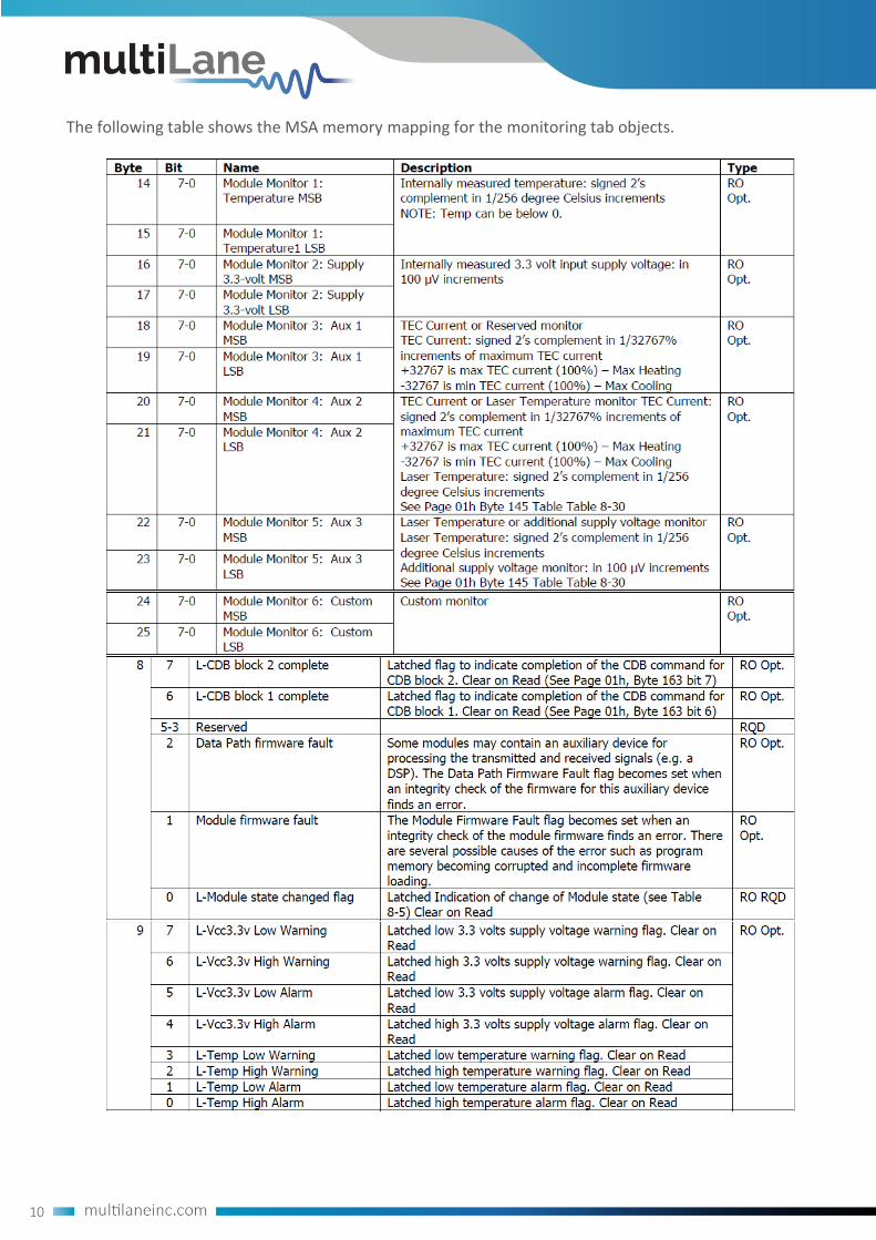
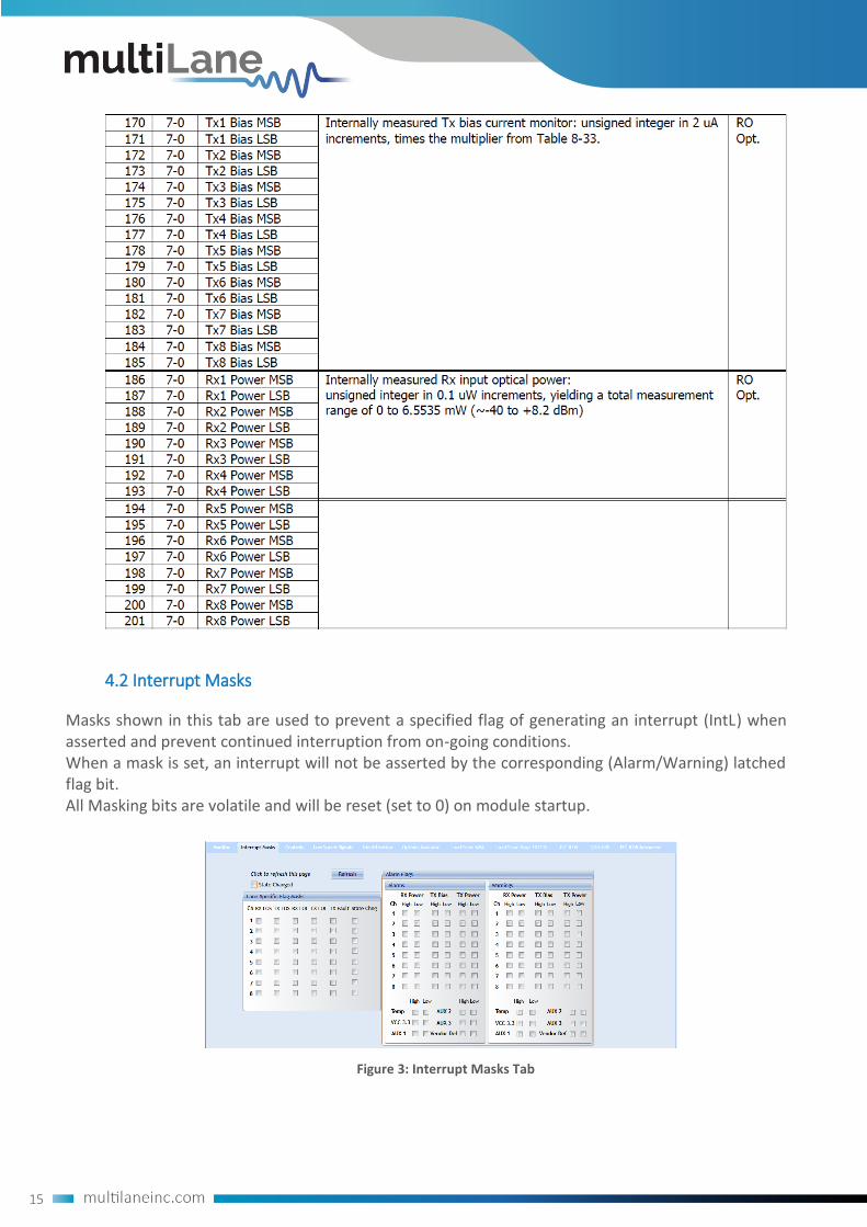
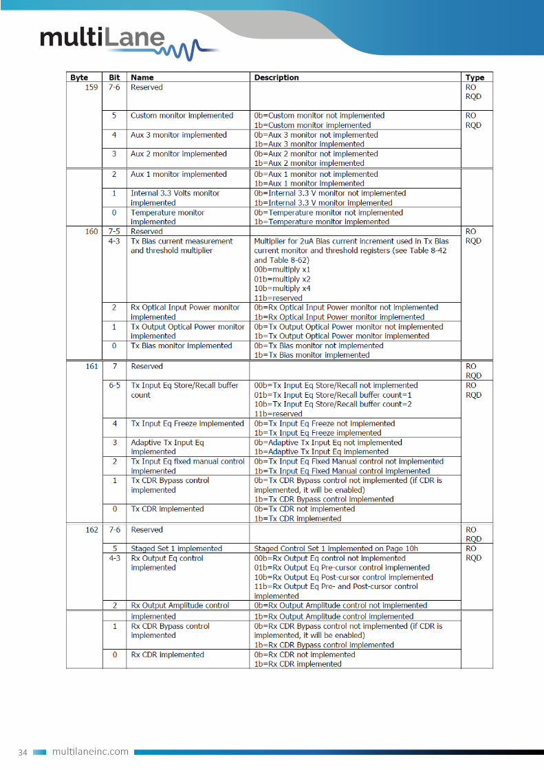
The following table shows the MSA memory mapping for the monitoring tab objects.

11

12
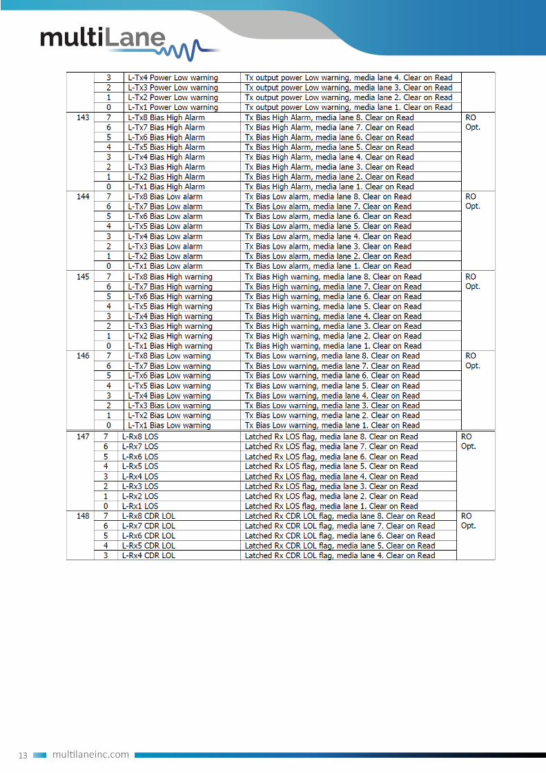
13

14
15
4.2 Interrupt Masks
Masks shown in this tab are used to prevent a specified flag of generating an interrupt (IntL) when asserted and prevent continued interruption from on-going conditions. When a mask is set, an interrupt will not be asserted by the corresponding (Alarm/Warning) latched flag bit. All Masking bits are volatile and will be reset (set to 0) on module startup.
Figure 3: Interrupt Masks Tab
16
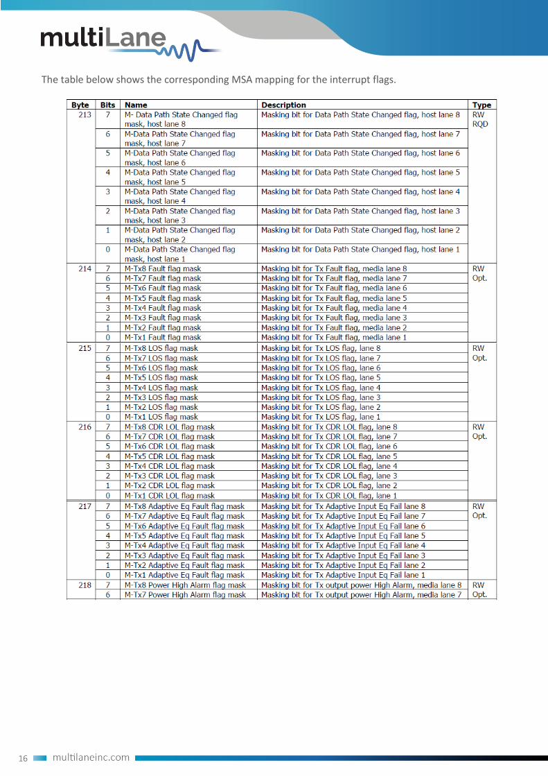
The table below shows the corresponding MSA mapping for the interrupt flags.

17

18

19

20
4.3 Controls
The control fields allow the host to dynamically change the behavior of the device. It allows the user to control Tx Input Equalization, Rx amplitude, Rx Pre-Cursor and Rx Post-Cursor. The User should follow this procedure:
▪ Set values to the control fields.
▪ Apply the configuration by selecting either ApplyDataPathInit or ApplyImmmediate.
▪ Press one of the 2 buttons (Apply All or Apply Lane) depending on user need.
▪ The module copies the data to the Active set.
▪ If the DataPathPwrUp is set, this applied configuration will be applied to the hardware.
Also this tab allows the user to control the module voltage, in case of the MCB is supplied by dual supply (5V and 3.3V). Three voltage levels are available: 3.15V, 3.3V and 3.45V.

21
Figure 4: MCB Voltage Control
Figure 5: Control Tab
The following table shows the corresponding registers, along with their names and description.

22

23

24
The optional controls follow this flow diagram.
Figure 6: Control Set Data Flow Diagram

25

26

27
4.4 Low Speed Signals
This tab allows to control and monitor the HW signals, depending on the selected device. The sections below define the control signals for each group of devices that share the same HW signals, separately.
4.4.1 QDD Family
This family includes MCBs like ML4062-MCB, ML4062-MCB-MXP and ML4062-TR. Module Input signals:
LPMode: ▪ If set to Low: Module is in High Power Mode ▪ If set to High: Module is in Low Power Mode
ResetL: ▪ If set to Low: Module is in Reset state ▪ If set to High: Module is out of Reset state
ModSelL: ▪ If set to Low: Module is selected and I2C communication is active ▪ If set to High: Module is not selected and I2C communication is inactive
28
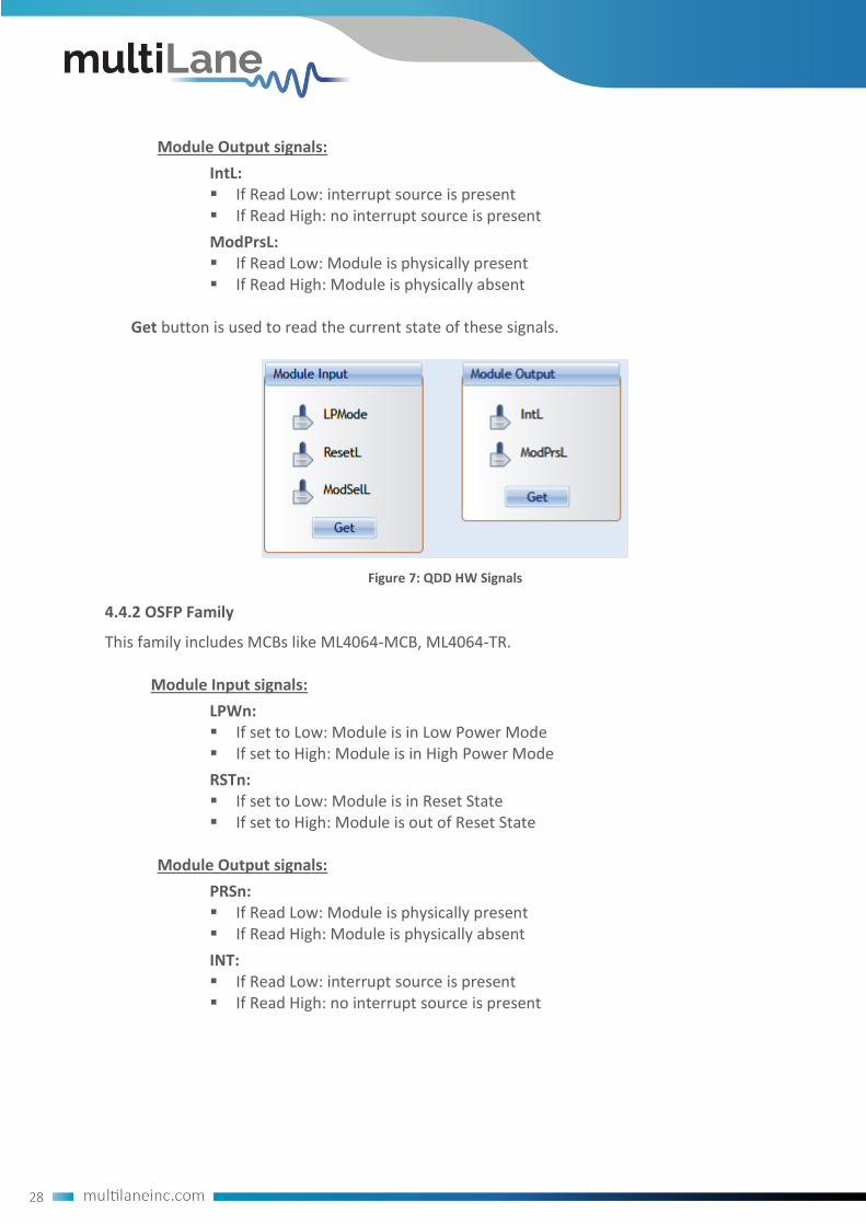
Module Output signals:
IntL: ▪ If Read Low: interrupt source is present ▪ If Read High: no interrupt source is present
ModPrsL: ▪ If Read Low: Module is physically present ▪ If Read High: Module is physically absent
Get button is used to read the current state of these signals.
Figure 7: QDD HW Signals
4.4.2 OSFP Family
This family includes MCBs like ML4064-MCB, ML4064-TR. Module Input signals:
LPWn: ▪ If set to Low: Module is in Low Power Mode ▪ If set to High: Module is in High Power Mode
RSTn: ▪ If set to Low: Module is in Reset State ▪ If set to High: Module is out of Reset State
Module Output signals:
PRSn: ▪ If Read Low: Module is physically present ▪ If Read High: Module is physically absent
INT: ▪ If Read Low: interrupt source is present ▪ If Read High: no interrupt source is present
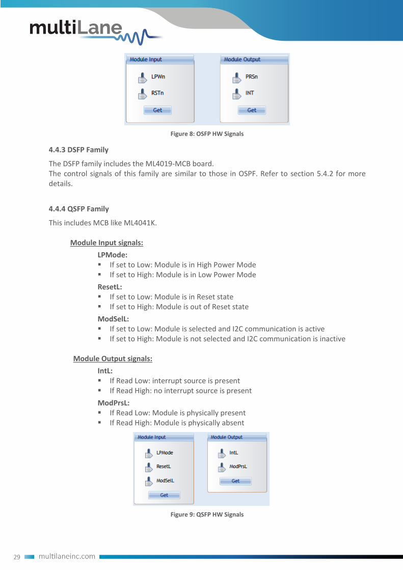
29
Figure 8: OSFP HW Signals
4.4.3 DSFP Family
The DSFP family includes the ML4019-MCB board. The control signals of this family are similar to those in OSPF. Refer to section 5.4.2 for more details.
4.4.4 QSFP Family
This includes MCB like ML4041K.
Module Input signals:
LPMode: ▪ If set to Low: Module is in High Power Mode ▪ If set to High: Module is in Low Power Mode
ResetL: ▪ If set to Low: Module is in Reset state ▪ If set to High: Module is out of Reset state
ModSelL: ▪ If set to Low: Module is selected and I2C communication is active ▪ If set to High: Module is not selected and I2C communication is inactive
Module Output signals:
IntL: ▪ If Read Low: interrupt source is present ▪ If Read High: no interrupt source is present
ModPrsL: ▪ If Read Low: Module is physically present ▪ If Read High: Module is physically absent
Figure 9: QSFP HW Signals

30
4.4.5 SFP-DD Family
This includes MCB like ML4022-MCB.
Module Input signals:
LPMode: ▪ If set to Low: Module is in High Power Mode ▪ If set to High: Module is in Low Power Mode
TxDisable0/ TxDisable1: ▪ Set to Low or High by the user for CH0 and CH1 respectively
Module Output signals:
TxFault0/TxFault1: ▪ Output state (Low or High) from the Module for CH0 and CH1 respectively
RXLOS0/RXLOS1: ▪ Output state (Low or High) from the Module for CH0 and CH1 respectively
User should click on Refresh button to get the current output signals state.
Rate Select HW Control Contacts:
Speed0-1/ Speed 1-1: ▪ Set the rate of the Receiver for CH0 and CH1 respectively
Speed0-2/ Speed 1-2: ▪ Set the rate of the Transmitter for CH0 and CH1 respectively
Reserved Pins:
RSVD / RSVD2: ▪ As Output: pins are set to High or Low ▪ As Input: Pins are Tri-stated
Figure 10: SFP-DD HW Signals

31
4.5 Identification
The Identification tab summarizes module specifications, vendor information and others.
Figure 11: Identification Tab
The following table shows the corresponding ID registers, along with their names and description.

32
4.6 Options Available
This tab specifies the options implemented in the module.
Figure 12: Options Available Tab
The following table shows the corresponding registers, along with their names and description.

33
34

35
4.7 Load/Save MSA
This tab allows the user to Load or Save his custom MSA configuration. Data is displayed in a grid showing: register address, hex value, Decimal Values, ASCII value, MSA description. Also the buttons available in this tab are summarized below:
▪ Refresh Page: Read MSA Registers, and refresh values.
▪ Write MSA to HW: Write the current MSA configuration to the module.
▪ Save MSA to file: Save the current MSA memory to a file using Comma separated values (CSV) format.
▪ Load MSA from file: Load MSA values from file and map it to MSA memory.
▪ Checksum for pages 00, 01 and 02
Figure 13: Load/Save MSA Tab
4.8 Load/Save Page 10/11h
This tab allows the user to Load or Save configuration for Page10h and Page11h. Data is displayed in a grid showing: register address, hex value, Decimal Values, ASCII value and MSA description. Buttons in this tab are described below:
▪ Refresh Page: Read Registers, and refresh values.
▪ Write MSA to HW: Write the current MSA configuration to the module.
▪ Save MSA to file: saves the current MSA memory to a file using Comma separated values (CSV) format.
▪ Load MSA from file: Loads MSA values from file and map it to MSA memory.

36
Figure 14: Load/Save Page 10/11h Tab
4.9 I2C R/W
This tab gives access to MSA registers. 1. Select the page in the Memory Location.
2. Single Byte window: to read/write one byte from the memory. a. Address: The address to read/write from.
b. Memory Content: The data value read from or written to the selected address. 3. Multi-bytes window: to read multiple bytes between selected Starting Address and an End Address.
Figure 15: I2C R/W Tab
37
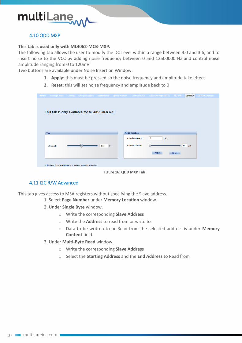
4.10 QDD MXP
This tab is used only with ML4062-MCB-MXP. The following tab allows the user to modify the DC Level within a range between 3.0 and 3.6, and to insert noise to the VCC by adding noise frequency between 0 and 12500000 Hz and control noise amplitude ranging from 0 to 120mV. Two buttons are available under Noise Insertion Window:
1. Apply: this must be pressed so the noise frequency and amplitude take effect
2. Reset: this will set noise frequency and amplitude back to 0
Figure 16: QDD MXP Tab
4.11 I2C R/W Advanced
This tab gives access to MSA registers without specifying the Slave address. 1. Select Page Number under Memory Location window.
2. Under Single Byte window.
o Write the corresponding Slave Address
o Write the Address to read from or write to
o Data to be written to or Read from the selected address is under Memory Content field
3. Under Multi-Byte Read window.
o Write the corresponding Slave Address
o Select the Starting Address and the End Address to Read from

38
Figure 17: I2C R/W Advanced Tab
4.12 Command Data Block (CDB) Message Communication
The Common Data Block (CDB) is a message communication protocol between the Host and a Module that allows the user to check and apply various settings on the interconnect, including updating the firmware. CDB is a Two Wire serial Interface (TWI) protocol based on the i2c for CMIS 4.0 and 5.0 between a Master (Initiator in 5.0) and Slave (Target in 5.0). The host sends a CDB Command (CMD) message which is identified by a CMD ID and the module responds with a CDB Reply (REPLY) message without changing the CMD ID. On the ML4062 Module Compliance Board (MCB), the CDB enables the issuing of commands from the MCB to the interconnect. The ML4062 MCB includes all CDB commands mentioned in CMIS 4.0 and CMIS 5.0.
Unlock CDB feature by loading the purchased License File:
Figure 21: CDB License Validation

39
4.12.1 CDB Commands
▪ CMD 0000h Query Status
▪ CMD 0001h Enter Password
▪ CMD 0002h Change Password
▪ CMD 0003h Enable/Disable Password Protection
▪ CMD 0004h General Abort
▪ CMD 0380h Loopbacks
The CDB GUI includes detailed map registers that show what is returned by each command. Here, for example, the query status command is being sent. A progress bar indicates the progress of the running CDB command. The GUI clearly indicates that the command was sent successfully (CDB status=1), that it asserts the CDB flag, and that it returns three bytes of data as shown with the corresponding value and description. The User can export this data (to an excel sheet) using the export button.
Figure 22: CDB Commands

40
4.12.2 CDB Feature and Capabilities Commands
▪ CMD 0040h Module Features: Identifies which commands are supported, from CMD 0 to CMD 00FF along with the maximum CDB command execution time.
▪ CMD 0042h Performance Monitoring: Identifies which commands are supported from 0200h to 02FFh.
▪ CMD 0043h Bert and diagnostics: Identifies CMD 0300h to 03FFh.
▪ CMD 0041h Read FW Features: Identifies many parameters supported the firmware features including firmware download transfer type, if copy/abort/full image readback commands are supported, start command payload size, erased byte, the firmware update features, if read/write firmware is supported, the firmware can be upgraded, etc. Use this feature to determine whether a device supports LPL or EPL firmware.
The green buttons indicate which commands are supported. In this case, the module feature command is returning the corresponding data in the detailed map register and indicates that CMDs 0,1,2,40,41,42,43 are supported (other modules might support other commands).
4.12.3 CDB Firmware Download Commands
▪ CMD 0101h, 0103h, 0107h Program LPL: Loads the firmware binary file for Local Payload (LPL). Allows for updating interconnect firmware.
▪ CMD 0101h, 0104h, 0107h Program EPL: Loads the firmware binary file for Extended Payload (EPL). EPL support varies depending on the interconnect. Allows for updating interconnect firmware.
▪ CMD 0101h, 0105h, 0107h Read Image LPL: Read the latest upgraded firmware image using LPL
Figure 23: CDB Feature and Capabilities Commands

41
▪ CMD 0101h, 0106h, 0107h Read Image EPL: Read the latest upgraded firmware image using EPL.
▪ Export Image: Exports an image of the firmware after the read is completed as a .bin file, which in turn can be loaded into and read by other interconnects.
▪ CMD 0102h Abort FW download: Stops the firmware from being installed onto the interconnect.
▪ CMD 0109h Run image: After the new LPL or EPL Firmware is loaded, this command switches to the latest firmware image. Does not replace the existing firmware image on the interconnect.
▪ CMD 010Ah Commit image: Replaces the firmware image on the interconnect with the new loaded firmware image. Prior to this command being executed, the old firmware will still be executed on startup. Always ensure the new image is running perfectly (by running it on the interconnect using the previous commands) before using this command.
▪ CMD 0108h Copy image A to B/B to A: In the event of two images being present on the same interconnect and both images are written to flash, this command makes ensures that both images are identical, with the copied image being specified in the commands as either image A to image B, or image B to image A.
▪ CMD 0100h Get FW Info: Loads the information about the latest firmware on the interconnect, for both image A and image B.
4.12.4 CDB Performance/Data Monitoring Commands
▪ CMD 0200h PM Controls: Extract Performance Monitoring data records such as minimum/average/maximum values. “No Operation” reads the most recent values, while “Clear All” clears the extracted values for all lanes in the interconnect.
Figure 24: CDB Firmware Download Commands

42
▪ CMD 0201h PM Feature Information: Reads the PM’s additional features.
▪ CMD 0280h Data Monitoring and Recording Controls: “Refresh” loads the most recent attributes. “Clear All” clears all values for all parameters for all lanes at the same time.
▪ CMD 0281h Data monitoring and recording advertisement
▪ CMD 0290h Temperature Histogram: Displays the temperature intervals of the interconnect and how long it stayed at each temperature interval.
▪ CMD 0210h, 0211h Get Module PM LPL/EPL: Choose parameters of the module’s performance monitoring records, and replace the current values of the minimum, average, and maximum values. “Refresh” replaces the old values, while “Clear and Read” reads and resets the old values.
▪ CMD 0212h, 0213h Get PM Host Side LPL/EPL: Choose parameters of the host’s performance monitoring records, and replace the current values of the minimum, average, and maximum values. “Refresh” replaces the old values, while “Clear and Read” reads and resets the old values.
▪ CMD 0214h, 0214h Get PM Media Side LPL/EPL: Choose parameters the performance monitoring records of specific lanes, and replace the current values of the minimum, average, and maximum values. “Refresh” replaces the old values, while “Clear and Read” reads and resets the old values.
▪ CMD 0216h, 0217h Get Data Path PM LPL/EPL: Choose the data path for specific lanes and replace the current values of the minimum, average, and maximum values. “Refresh” replaces the old values, while “Clear and Read” reads and resets the old values.
Figure 25: CDB Performance/Data monitoring Commands
43
Software Revision
V2.2.1: latest Software Revision, which this document is based on.

44
North America Worldwide Asia
48521 Warm Springs Blvd. Suite 310 Houmal Technology Park 14F-5/ Rm.5, 14F., No 295 Fremont, CA 94539 Askarieh Main Road Sec.2, Guangfu Rd. East Dist., USA Houmal, Lebanon Hsinchu City 300, Taiwan (R.O.C) +1 510 573 6388 +961 81 794 455 +886 3 5744 591
Figure 18: Setup Installation Procedure North America Worldwide
Asia
48521 Warm Springs Blvd. Suite 310 Houmal Technology Park 14F-5/ Rm.5, 14F., No 295 Fremont, CA 94539 Askarieh Main Road Sec.2, Guangfu Rd. East Dist., USA Houmal, Lebanon Hsinchu City 300, Taiwan (R.O.C) +1 510 573 6388 +961 81 794 455 +886 3 5744 591