Interface Unit
185
Interface Unit ASTRODESIGN, Inc. VG Series Instruction Manual Ver. 2.50
-
Upload
khangminh22 -
Category
Documents
-
view
0 -
download
0
Transcript of Interface Unit

Interface Unit
ASTRODESIGN, Inc.
VG Series
Instruction Manual Ver. 2.50

Before Operation
2
Before Operation
Introduction
Thank you for purchasing the VG Series programmable video signal generator.
This Instruction Manual (called “this manual” below) explains how to use the VG Series interface units and provides information that
you should know before using them. Be sure to read this manual and use the unit correctly.
Keep this manual in a safe place for later reference.
Notational Conventions
For conciseness, this manual uses the following shorter descriptions for some terms.
Item Term used in this manual
VG Series Interface Units System

Contents
3
Contents
Before Operation ...................................................................2
Introduction .............................................................. 2
Notational Conventions ........................................... 2
Contents ...............................................................................3
Chapter 1 VG Series Interface Unit Overview ........5
1.1 Relationship between interface unit and
compatible products ........................................ 5
Chapter 2 Common Setting Items
(ALL OUTPUT) ................................................6
2.1 ALL OUTPUT .................................................. 6
Chapter 3 Analog Output Settings
(ANALOG OUTPUT) ................................... 10
3.1 Analog unit functions and settings ................ 10
3.1.1 Analog Unit VM-1876-MA ................... 10
3.1.2 Internal analog output section ............. 11
3.1.3 Connector and pin assignment ........... 13
3.1.4 Setting item ......................................... 15
3.2 TV standard signal functions ........................ 16
3.2.1 Explanation of terms ........................... 16
3.2.2 Setting item ......................................... 21
Chapter 4 Digital Output Settings
(DIGITAL OUTPUT)..................................... 29
4.1 HDMI unit functions and settings .................. 29
4.1.1 HDMI unit VM-1876-M0 and
VM-1876A-M0 ..................................... 29
4.1.2 HDMI 6G Unit VM-1876-M6,
VM-1876A-M6 ..................................... 31
4.1.3 HDMI HDCP2.2 Unit VM-1876-M7 ..... 33
4.1.4 HDMI 6G HDCP2.2 Unit
VM-1876-M8........................................ 35
4.1.5 HDMI 2.1 Unit VM-1876-MD .............. 37
4.1.6 Internal HDMI output section .............. 43
4.1.7 Connector and pin assignment ........... 45
4.1.8 HDMI data transfer method ................. 46
4.1.9 Output setting items ............................ 50
4.1.10 HDMI configuration setting items ........ 60
4.1.11 Relationship between Pattern Rendering
Bit Length and Dot Clock .................... 63
4.2 DisplayPort unit functions and settings ........ 67
4.2.1 DisplayPort Unit VM-1876A-M1 .......... 67
4.2.2 Connector and pin assignment ........... 70
4.2.3 DisplayPort data transfer method ....... 71
4.2.4 DisplayPort output setting items ......... 78
4.2.5 DisplayPort configuration setting items ..
............................................................ 83
4.2.6 DP Analysis setting items .................... 84
4.2.7 Displaying setting information as
patterns ............................................... 86
4.2.8 Relationship between Pattern Rendering
Bit Length and Dot Clock .................... 89
4.3 SDI unit functions and settings ..................... 96
4.3.1 SDI Unit VM-1876-M5 ......................... 96
4.3.2 12G-SDI Unit VM-1876-MB ................ 96
4.3.3 SDI data transfer method .................. 102
4.3.4 SDI output setting items .................... 103
4.3.5 Payload ............................................. 104
4.3.6 SDI configuration setting items ......... 107
4.4 V-by-One HS unit functions and settings .... 110
4.4.1 V-by-One HS Unit VM-1876-M2 ....... 110
4.4.2 Connector and pin assignment ..........111
4.4.3 V-by-OneHS data transfer method ... 112
4.4.4 V-by-One HS output setting items .... 129
4.4.5 V-by-One HS configuration setting items
.......................................................... 131
4.4.6 V-by-One HS control ......................... 131
4.4.7 Relationship between Pattern Rendering
Bit Length and Dot Clock .................. 132
4.5 iTMDS unit functions and settings .............. 134
4.5.1 iTMDS Unit VM-1876-M9 .................. 134
4.5.2 Connector and pin assignment ......... 135
4.5.3 iTMDS data transfer method ............. 136
4.5.4 iTMDS output setting items ............... 151
4.5.5 Polarity setting of synchronization signal
.......................................................... 152
4.5.6 Relationship between Pattern Rendering
Bit Length and Dot Clock .................. 153

Contents
4
4.6 HDBaseT unit functions and settings.......... 155
4.6.1 VM-1876-MC output .......................... 155
4.6.2 Connector and pin assignment ......... 157
4.6.3 HDBaseT data transfer method ........ 157
4.6.4 Output setting items .......................... 158
4.6.5 HDBaseT Config Setting Item ........... 167
4.7 Synchronization unit (multiple VG unit
synchronization) functions and settings ...... 169
4.7.1 VM-1876-MX output parts ................. 169
4.7.2 Overview of synchronization operation ...
........................................................... 170
4.7.3 Connection method ........................... 171
4.7.4 Image of splitting method when
synchronizing 4 units ......................... 172
4.7.5 Image of splitting method when
synchronizing 2 units ......................... 176
4.7.6 Scanning direction image .................. 178
4.7.7 Synchronization unit setting items .... 180
4.7.8 Control method .................................. 182
Chapter 5 Appendix ...................................................... 183
5.1 DDC power supply max power current
consumption ................................................ 183
5.2 Trademarks ................................................. 183
Chapter 6 Revision History ....................................... 184

Chapter 1 VG Series Interface Unit Overview
5
Chapter 1 VG Series Interface Unit Overview
1.1 Relationship between interface unit and compatible products
The interface units included in the VG Series differ depending on the product.
See the following table for information on the relationship between your product and compatible interface units.
Model number Interface name / explanation
section
Applicable models
VG-876 VG-877 VG-878 VG-878-A VG-879
VM-1876-MA 3.1.1 Analog Unit ○ ○ - - ○
Internal Analog Output
Section
3.1.2 Internal Analog Unit - - ○ ○ -
VM-1876-M0
VM-1876A-M0
4.1.1 HDMI Unit ○ ○ - - ○
VM-1876-M6
VM-1876A-M6
4.1.2 HDMI 6G Unit ○ ○ - - ○
VM-1876-M7 4.1.3 HDMI HDCP 2.2 Unit ○ ○ - - ○
VM-1876-M8 4.1.4 HDMI 6G HDCP 2.2 Unit ○ ○ - - ○
Built in HDMI Output
Section
4.1.6 Internal HDMI Unit - - ○ ○ -
VM-1876-M1 4.2.1 DisplayPort Unit ○ ○ - - ○
VM-1876A-M1 4.2.2 DisplayPort Unit ○ ○ - - ○
VM-1876-M5 4.3.1 SDI Unit ○ - - - -
VM-1876-MB 4.3.2 SDI 12G Unit - ○ - - ○
VM-1876-M2 4.4.1 V-By-One HS Unit ○ ○ - - ○
VM-1876-M9 4.5.1 iTMDS Unit ○ - - - ○
VM-1876-MX 4.6.1 Synchronization Unit ○ - - - ○
VM-1876-MC 4.7.1 HDBaseT Unit ○ ○ - - ○
VM-1876-MD 4.1.5 HDMI2.1 Unit - - - - ○
・ Set “ON” of “VM-1876-MD Mode” in 「4.1.10 HDMI configuration setting items」.
・ If you output other VMs except VM-1876-MD, set “OFF” of “VM-1876-MD Mode”
・ If you set “ON” of “VM-1876-MD Mode”, other boards does not output signal.
・ When 8K timing is output, scroll is not supported.

Chapter 2 Common Setting Items (ALL OUTPUT)
6
Chapter 2 Common Setting Items (ALL OUTPUT) This section describes setting items common to all interface units.
The following items show settings common to multiple video and audio output interfaces.
Item
Output interface ON/OFF settings
Synchronization ON/OFF and polarity settings
Level mode settings
Dot clock operation mode (DotClk Mode) settings
Aspect ratio settings
Pattern rendering Color Depth (gradation) settings
RGB/YPbPr selection and color difference coefficient settings
Digital Level settings
2.1 ALL OUTPUT
Common setting item details for each unit are as follows.
Level 1 Level 2 Level 3 Setting item Setting value
All
Output
Output OFF/ON
Sets output ON/OFF for
each output terminal.
HDMI [VG-876,877] Port1 to Port16 0: OFF / 1: ON
[VG-878,878-A] Port1 to Port4
DP Port1 to Port8
V-by-One HS Port1 to Port16
SDI Port1 to Port16
iTMDS Port1 to Port8
Analog [VG-876, 877]
VGA1 to 4
YPbPr1 to 4
Composite1 to 4
[VG-878,878-A]
VGA, YPbPr, Composite, Y/C,
SCART
HDBaseT Port 1 to 16
Sync
Sets synchronization signal ON/OFF, and
polarity settings for each output terminal.
Note) VM-1876-MD does not support this item.
HS Sets output for the HS terminal.
0: OFF No output.
1: Nega Output as
negative polarity.
2: Posi Output as
positive polarity.
VS Sets output for the VS terminal.
0: OFF No output.
1: Nega Output as
negative polarity.
2: Posi Output as
positive polarity.
CV Sets Video-On-Sync superimposition for the analog component signal.
0: OFF / 1: R / 2: G / 3:
RG / 4: B / 5: RB / 6: GB
/ 7: RGB
HDCP
(Note: this item is in “HDMI Output” on VG-
878,878-A)
Execute Enable 0: Disable / 1: Enable
Port Type (*VG-876, 877 and VG-
879 only)
0: HDMI / 1: DP/
2: HDBaseT
Port No. [VG-876, 877, 879]
(HDMI) 0 to 16

Chapter 2 Common Setting Items (ALL OUTPUT)
7
Level 1 Level 2 Level 3 Setting item Setting value
All
Output
Sets which output port information to display when displaying the HDCP pattern.
[VG-878,878-A]
0: Disable,
1 to 4: HDMI1 to HDMI4
HDCP Auth Version 0: Auto
(* In HDMI Output on VG-878,878-A) Set the HDCP version. 1: HDCP1.4
Relies on the connection destination
supported version when set to Auto.
2: HDCP2.3
Level Mode
(This item is In Analog Output and HDMI
Output on VG-878,878-A)
HDMI 0: Full / 1: Limited
DP
SDI
V-by-One HS
iTMDS
Analog (for VG-876/877)
HDBaseT
DotClk Mode
● In Auto, single/dual/quad clock modes are
automatically selected according to dot clock.
Screen splitting method is disabled.*
● When Auto is selected on the V-by-One®HS
unit and iTMDS unit, the number of data lanes
automatically switches according to
single/dual/quad clock mode.
0: Auto Operates by automatically selecting the clock mode from
the dot clock.
1: Single Operates as single clock mode.
2: Dual Operates as dual clock mode (double speed).
3: Quad Operates as quad clock mode (quadruple speed).
The following Split Mode setting is displayed when dual clock
mode and quad clock mode are set.
Split Mode For dual clock mode Setting unit
MODE0(HDiv) 2 panes horizontal
output
H: 2dot V: 2line
MODE1(VDiv) 2 panes vertical
output
H: 4dot V: 1line
MODE2(HDiv) 2 panes horizontal
output
H: 2dot V: 2line
MODE3(VDiv) 2 panes vertical
output
H: 4dot V: 1line
MODE4(No Div) No divisions H: 4dot V: 1line
MODE5(No Div) No divisions H: 4dot V: 1line
MODE6(No Div) No divisions H: 4dot V: 1line
MODE7(No Div) No divisions H: 4dot V: 1line
MODE8(VDiv) 2 panes vertical
output
H: 4dot V: 1line
MODE9(VDiv) 2 panes vertical
output
H: 4dot V: 1line
For quad clock mode Setting unit
MODE0(H2/V2Div) 4 quarter panes H: 4dot V: 2line
MODE1(V4Div) 4 panes vertical H: 4dot V: 1line
MODE2(H2/V2Div) 4 quarter panes H: 4dot V: 2line
MODE3(V4Div) 4 panes vertical H: 4dot V: 1line
MODE4(V2Div) 2 panes vertical H: 4dot V: 1line
MODE5(V2Div) 2 panes vertical H: 4dot V: 1line
MODE6(V2Div) 2 panes vertical H: 4dot V: 1line
MODE7(V4Div) 4 panes vertical H: 4dot V: 1line
MODE8(V4Div) 4 panes vertical H: 4dot V: 1line
MODE9(No Div) No divisions H: 4dot V: 1line
MODE10(2SI) 2-sample Interleave
Division
H: 4dot V: 2line
For the V-by-One HS unit and iTMDS unit, it is possible to set more than 4 panes using Split
Mode settings.

Chapter 2 Common Setting Items (ALL OUTPUT)
8
Level 1 Level 2 Level 3 Setting item Setting value
All
Output
Multi VGMode(* VG-876 and VG-879 only)
Sets the splitting method for each VG1 when
multiple VG units are synchronized.
Note) the setting image is displayed like the below
pop-up image.
0: Auto Default is 4 quarter panes
When Dot Clock exceeds 1320MHz, it split into Tile
split mode. When 1320MHz or less, it does not split.
1: H2/V2Div 4 quarter panes
2: V4Div 4 vertical panes
3: V2Div 2 vertical panes
Aspect Mode: Sets the video signal aspect ratio.
Normal images are output at a ratio of 4:3,
however, because images are output as 16:9 when
4:3 Letter Box is selected, black bars will appear on
the top and bottom of images.
Images are output in the following way when 4:3
Letter Box is selected.
0: 4:3
1: 4:3 Letter Box * 4:3 Letter Box settings are only available for SDTVTiming.
2: 16:9
3: Resolution The aspect ratio can be set at the same ratio as screen resolution.
4: User Sets any aspect ratio.
H Sets the horizontal
direction aspect
ratio.
Setting range: 0 to
255
V
Sets the vertical
direction aspect
ratio.
Setting range: 0 to
255
* When output at a 21:9 ratio, set the Aspect Mode to
User, H = 21 and V = 9.
Color Depth
The Color Depth (gradation) can be set for
rendering a test pattern.
The following two options are available: setting
individually for each Program, or locking the Color
Depth regardless of the Program.
Set the Color Depth for each Program in this
menu.
* To specify a constant Color Depth, go to
MENU. > Configuration > General
8bit to 16bit
4: When normal
16: When letter box
9:
letter box 3:
normal

Chapter 2 Common Setting Items (ALL OUTPUT)
9
RGB/YPbPr (0/1):
(* In Analog Output on VG-878,878-A)
0: RGB / 1: YPbPr Selects the output color
difference mode.
The color difference coefficient is applied for YPbPr (YCbCr) output.
YPbPr Select(0-4): 0: SMPTE274M/296M/RP-177
1: SMPTE240M
2: SMPTE293M
3: SMPTE125M
4: User
5: ITU-R BT.2020
Sets User and any
coefficient.
Sets any color difference coefficient when User is selected above.
User YPbPr Coefficient Y (The total for line Y must be 1.0000.)
Sets Y/Pb/Pr items.
Pb (The coefficient totals for Pb and Pr must be 0.)
Pr

Chapter 3 Analog Output Settings (ANALOG OUTPUT)
10
Chapter 3 Analog Output Settings (ANALOG OUTPUT)
3.1 Analog unit functions and settings
The applicable unit is as follows.
3.1.1 Analog Unit VM-1876-MA
● Unit exterior diagram
No. Name Description
① Component output Can output YPBPR analog component signals. (RCA connector)
② VGA output
Can output analog component signal (RGB) and H/V separate sync. (DSUB connector,
shrink D-Sub 15-pin)
③ CVBS output Can output NTSC/PAL composite (VBS) signal. (RCA connector)
④ Analog audio output Can output analog audio (L/R). (RCA connector)
⑤ Standby LED
Lights when output preparation is complete. On: Normal Off: Error (module damaged, wrong slot, etc.)
● Specifications
VGA
DotCLK 5 to 165 MHz
Number of colors, bit length RGB - 8 bit each
Connector Dsub x1
YPbPr
Resolution HDTV, SDTV
Number of colors, bit length YPbPr - 8 bit each
Connector RCA x3
CVBS
Resolution NTSC-M/J/443, PAL (B/D/G/H/I)/M/Nc
Number of colors, bit length YPbPr - 8 bit each
Connector RCA x1
Added functions Teletext, ClosedCaption, Vchip, Macrovision*
AUDIO
L/R
Output frequency 100 to 20 kHz (Sampling frequency: 48 kHz)
Output level 0 to 4000 mV
Connector RCA x2
* Macrovision function is available when a license is purchased.
① ② ③ ④
⑤

Chapter 3 Analog Output Settings (ANALOG OUTPUT)
11
3.1.2 Internal analog output section
● Unit exterior diagram
No. Name Description
① Analog audio output Can output analog audio (L/R). (RCA connector)
② Component output Can output YPBPR analog component signals. (RCA connector)
③ VGA output
Can output analog component signal (RGB) and H/V separate sync. (DSUB connector,
shrink D-Sub 15-pin)
④ SCART output
Can output NTSC/PAL/SECAM composite (VBS) signal, Y/C signal, analog component
signal (RGB), and analog audio. (SCART connector) [VG-878,878-A only]
⑤ CVBS output Can output NTSC/PAL composite (VBS) signal. (RCA connector)
⑥ Y/C output Can output Y/C signal (S terminal)
● Specifications(VG-878)
AUDIO
L/R
Output frequency 100 to 20 kHz (Sampling frequency: 48 kHz)
Output level 0 to 4000 mV
Connector RCA x2
YPbPr
Resolution HDTV, SDTV
Number of colors,
bit length YPbPr - 8 bit each
Connector RCA x3
VGA
DotCLK 5 to 165 MHz
Number of colors,
bit length RGB - 8 bit each
Connector Dsub x1
SCART
Resolution*1 NTSC-M/J/443, PAL-B/D/G/H/I/M/N/Nc/60, SECAM
Number of colors,
bit length YPbPr, RGB - 8 bit each
Connector SCART x1
Added functions*1 Teletext, ClosedCaption, Vchip, Macrovision*2
CVBS
Y/C
Resolution*1 NTSC-M/J/443, PAL-B/D/G/H/I/M/N/Nc/60, SECAM
Number of colors,
bit length YPbPr - 8 bit each
Connector RCA (CVBS) x1, S-Video (Y/C) x1
Added functions*1 Teletext, ClosedCaption, Vchip, Macrovision*2
*1 Parts of the TV option function and TV timing signal may not be supported on items other than VG-878.
*2 Macrovision function is available when a license is purchased.
① ② ③ ④ ⑤ ⑥

Chapter 3 Analog Output Settings (ANALOG OUTPUT)
12
● Specifications (VG-878-A)
AUDIO
L/R
Output frequency 100 to 20 kHz (Sampling frequency: 48 kHz)
Output level 0 to 4000 mV
Connector RCA x2
YPbPr
Resolution HDTV, SDTV
Number of colors,
bit length YPbPr - 8 bit each
Connector RCA x3
VGA
DotCLK 5 to 165 MHz
Number of colors,
bit length RGB - 8 bit each
Connector Dsub x1
SCART
Resolution*1 NTSC-M/J/443, PAL-B/D/G/H/I/M/Nc
Number of colors,
bit length YPbPr, RGB - 8 bit each
Connector SCART x1
Added functions*1 Teletext, ClosedCaption, Vchip, Macrovision*2
CVBS
Y/C
Resolution*1 NTSC-M/J/443, PAL-B/D/G/H/I/M/Nc
Number of colors,
bit length YPbPr - 8 bit each
Connector CVBS (RCA) x1, Y/C (S-Video) x1
Added functions*1 Teletext, ClosedCaption, Vchip, Macrovision*2
*1 Parts of the TV option function and TV timing signal may not be supported on items other than VG-878-A.
*2 Macrovision function is available when a license is purchased.

Chapter 3 Analog Output Settings (ANALOG OUTPUT)
13
3.1.3 Connector and pin assignment
● VGA (D-SUB) output
Pin No. Signal Pin No. Signal
1 R 9 +5 V (DDC power supply*1)
2 G 10 GND
3 B 11 GND
4 NC 12 DDC DATA
5 NC 13 HS
6 GND(R) 14 VS
7 GND(G) 15 DDC CLK
8 GND(B)
*1 The supply current of the DDC power supply is limited. Refer to “5.1DDC power supply max power current consumption“.
● YPbPr output
Connector name Signal
Y Y
PB Pb
PR Pr
● CVBS output
Connector name Signal
CVBS Composite video
10
5
1
6
15
11
Chapter 3 Analog Output Settings (ANALOG OUTPUT)
14
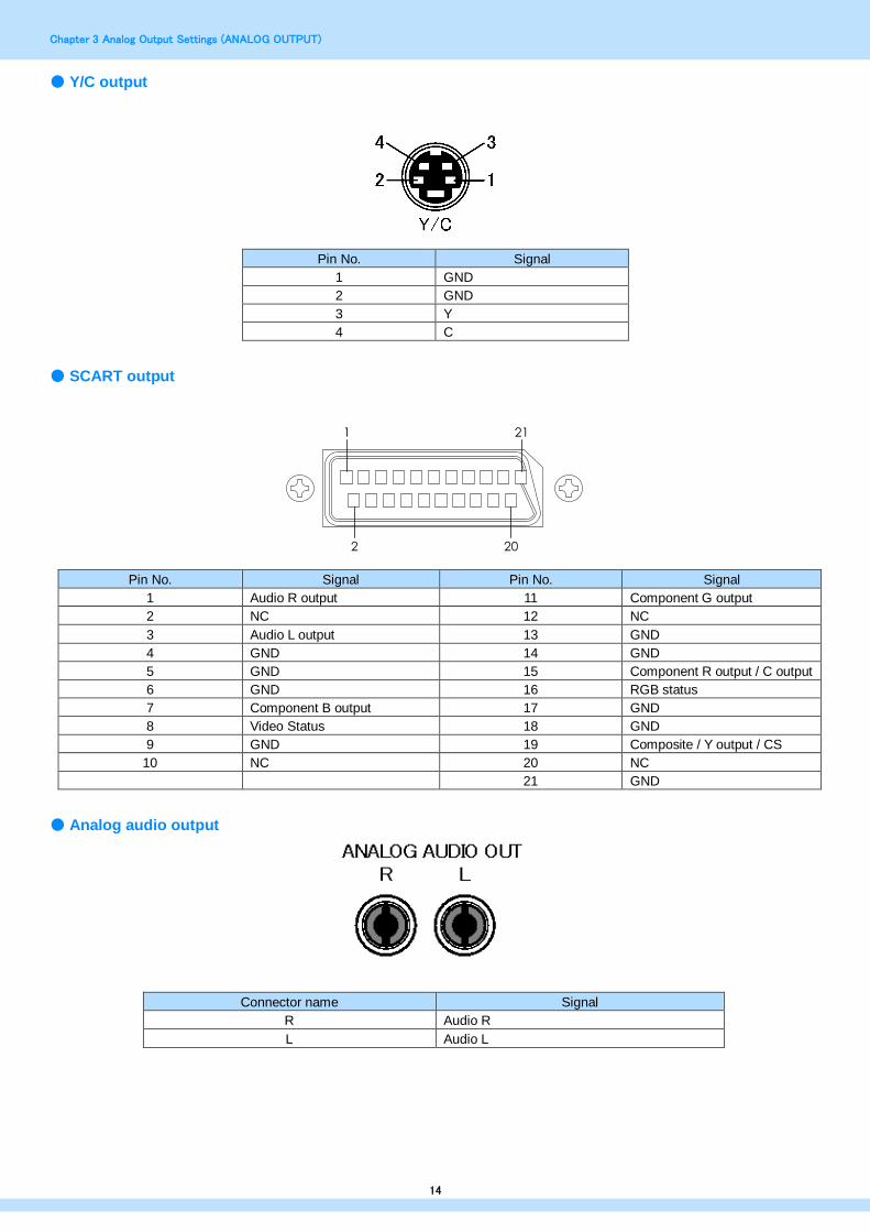
● Y/C output
Pin No. Signal
1 GND
2 GND
3 Y
4 C
● SCART output
Pin No. Signal Pin No. Signal
1 Audio R output 11 Component G output
2 NC 12 NC
3 Audio L output 13 GND
4 GND 14 GND
5 GND 15 Component R output / C output
6 GND 16 RGB status
7 Component B output 17 GND
8 Video Status 18 GND
9 GND 19 Composite / Y output / CS
10 NC 20 NC
21 GND
● Analog audio output
Connector name Signal
R Audio R
L Audio L
2
1
20
21

Chapter 3 Analog Output Settings (ANALOG OUTPUT)
15
3.1.4 Setting item
Level 1 Level 2 Level 3 Setting item Setting value
Analog Output
Output OFF/ON Sets ON/OFF for each Port.
[VG-876, 877, 879]
VGA1 to 4
YPbPr1 to 4
Composite1 to 4
0: OFF / 1: ON
[VG-878,878-A]
VGA
YPbPr
Composite
Y/C
SCART
0: OFF / 1: ON
General Sets the output signal for each program from the analog component signal, HS, and CS terminals. * Only available for VGA and YPbPr.
Level Video All Output Sync CV setting is
Other than
OFF
0.30 to 1.20 [V]
OFF 0.05 to 1.20 [V]
Setup Sets the setup level.
0.00 to 0.25 [V]
Sync Synchronization signal (Video-On-Sync)
0.00 to 0.60 [V]
Audio Output
Outputs analog audio.
0: OFF / 1: ON
Y/C Aspect (*VG-878,878-A only)
Set DC voltage for the C signal.
0: 4:3 Normal
1: 4:3 Letter Box
2: 16:9 Squeeze
3: Auto
Auto follows the
program aspect ratio
setting.
SCART (*VG-878,878-A only)
Output Select
Sets the video signal format output from
SCART.
0: Composite
1: Y/C
2: RGB
Video Status
Sets the Video Status signal output from
SCART.
0: Auto
1: 4:3
(Identification voltage
12 V (9.5 to 12.0 V))
2: 16:9
(Identification voltage
5 V (4.5 to 7.0 V))
3: No Signal
(Identification voltage
5 V (4.5 to 7.0 V))
RGB Status
Sets the RGB Status signal output from
SCART.
0: Auto
1: VBS
2: RGB
3: Fast Blanking
Configures the following settings when Fast Blanking is selected
above.
Fast Blanking Area:
Sets the Fast Blanking
output range.
H Sets the horizontal direction output range as a percentage for H-Disp.
Setting range: 0 to 100
[%]
V Sets the vertical
direction output range
as a percentage for H-
Disp.
Setting range: 0 to 100
[%]

Chapter 3 Analog Output Settings (ANALOG OUTPUT)
16
3.2 TV standard signal functions
3.2.1 Explanation of terms
● Macrovision
■ What is Macrovision?
This is a copy protection system developed by ROVI (formerly “Macrovision”).
It is used in a wide range of applications from VHS and DVD video to commercially available video sources and satellite
broadcasts. The copy protection system introduces an error into a VCR's AGC (Automatic Gain Control), making it impossible
to record the output source normally.
The AGC input signal gain is automatically adjusted to maintain the proper sensitivity via a circuit, and nearly all consumer
use VTRs contain this circuit. The function brightens and preserves dark screens and darkens video that is too bright.
The Macrovision copy protection signal introduces the AGC error by mixing in a non-standard level signal during the vertical
blanking period while maintaining the video signal brightness and color signal components. Therefore, even if recording is
possible, the screen brightness fluctuates. This signal also hinders the synchronization signal, scrambling the screen.
This impediment makes it impossible to dub an enjoyable video.
■ What is color striping?
Part of the Macrovision standard duplicates the normal Macrovision signal.
The altered color burst signal is superimposed on a video signal, and is also called color burst copy protection.
Color striping inserts thin horizontal lines into dubbed video, hindering enjoyment in the same way as Macrovision. * Color stripes are only applied to NTSC-M and J Type 2 and 3 modes.
■ Macrovision specifications
Macrovision is compatible with the following TV signals.
Macrovision is superimposed on composite signals, and Y/C signals.
・ NTSC-M, NTSC-J, NTSC-443
・ PAL-60, PAL, PAL-M, PAL-N, PAL-Nc
・ SECAM
■ Patent
Macrovision incorporates copyright protection technology protected by US patents and other intellectual property rights.
Permission from ROVI is required to use this copyright protection technology. Without permission from ROVI, it can only be used
for commercial testing purposes. Reverse engineering and disassembly are prohibited.
・Macrovision is an optional function. For details, contact a retailer or ASTRODESIGN, Inc. sales representative.
・The Macrovision signal operates differently depending on the VHS and DVD type. Make sure to check the contents of the
agreement with ROVI before use.

Chapter 3 Analog Output Settings (ANALOG OUTPUT)
17
● Closed captioning / V-Chip
■ What is closed captioning?
This is a subtitled broadcast developed in the US so that hearing impaired viewers can enjoy movies and news.
Because it does not appear on the screen during usual playback, it is called “closed.“ On the other hand, subtitles in Japanese
that are permanently embedded into video from the start are called “open captioning. “
Although CC technology was originally developed for visually impaired persons, it is now gaining attention as a tool to assist
educators, those engaged in language study, and for listening practice.
CC subtitle data is superimposed on and output from NTSC output line 21 (1st field) and line 284 (2nd field). Subtitle data
includes two modes: captions and text. Extended Data Service (EDS) is also available. This service uses line 284 (2nd field)
to transfer program information such as titles and ratings. The V-chip described later uses the EDS function.
Up to 32 characters per line can be displayed in CC. Although 15 lines are available, the maximum number of lines is limited
to 4 in caption mode (CC1 to 4). Up to 15 lines can be displayed in text mode (T1 to 4).
■ What is the V-chip?
The V-chip is a semiconductor chip that removes TV programs containing violent and sexual content. V stands for “violence”,
and this chip blocks programs which are rated according to extreme content. When ratings are set on a receiver (TV) that
includes a V-chip function, EDS rating information is decoded and automatically determined whether or not to output the
program to the screen.
■ Closed captioning/V-chip specifications
Closed captioning/V-chip are compatible with the following TV signals.
Closed captioning is superimposed on composite signals, and Y/C signals.
・ NTSC-M, NTSC-J, NTSC-443
・ PAL-60, PAL, PAL-M, PAL-N, PAL-Nc
* However, caption data is superimposed on 21 lines (334 lines) during 625-line timing (PAL, PAL-Nc) output.
Waveforms for closed captioning/V-chip are shown below. Color burst is followed with a sin wave called Clock Run-In, then start
bit. Start bit is always “001. “ Two bytes of data (Char1, Char2) are sent on each line. Char1 and Char2 are decoded from LSB,
and usually an odd parity is appended to MSB (Bit8).
Start Bit Character OneClock Run-In Character Two
s1 s2 s3 b0 b1 b2 b3 b4 b5 b6 p1 b0 b1 b2 b3 b4 b5 b6 p2
50IRE
0IRE
LSB LSB
Closed Caption / V-Chip (21Line System)

Chapter 3 Analog Output Settings (ANALOG OUTPUT)
18
● Teletext
■ What is teletext?
Teletext is the name of a system that multiplexes and sends text and graphic still image program data during the TV signal
vertical blanking interval. Program content includes subtitle broadcasts, news broadcasts, weather forecasts, stock
information, etc., with many countries adopting the European and Southeast Asian 625/50i system.
In teletext, 40 characters x 25 lines can be displayed per page (1 screen), from 100 to 899 pages.
■ Teletext specifications
Teletext is compatible with the following TV signals.
Teletext is superimposed on composite signals, and Y/C signals.
・ PAL (Does not include PAL-60, PAL-N, PAL-Nc)
The vertical blanking interval (VBI) and teletext waveform are shown below.
Teletext data is output in PAL signal vertical blanking interval lines 8 to 22 (1st field) and lines 321 to 335 (2nd field).
Additionally, data superimposed on line 1 is 45 bytes of Clock Run-IN and Framing Code data (42 bytes).
VBI waveform
Teletext waveform
Clock Run-In
66IRE
0IRE 1 0 1 0 1 0 1 0 1 0 1 0 1 0 1 0 1 1 1 0 0 1 0 0
FramingCode
2byte 1byte
45byte
Teletext
Chapter 3 Analog Output Settings (ANALOG OUTPUT)
19
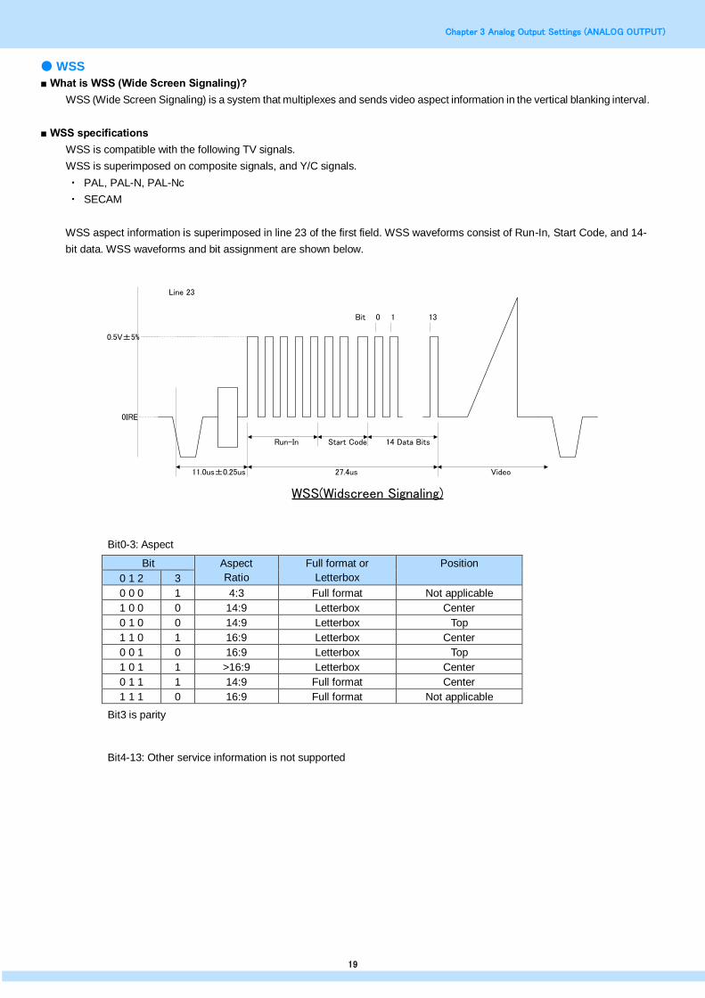
● WSS
■ What is WSS (Wide Screen Signaling)?
WSS (Wide Screen Signaling) is a system that multiplexes and sends video aspect information in the vertical blanking interval.
■ WSS specifications
WSS is compatible with the following TV signals.
WSS is superimposed on composite signals, and Y/C signals.
・ PAL, PAL-N, PAL-Nc
・ SECAM
WSS aspect information is superimposed in line 23 of the first field. WSS waveforms consist of Run-In, Start Code, and 14-
bit data. WSS waveforms and bit assignment are shown below.
Bit0-3: Aspect
Bit Aspect
Ratio
Full format or
Letterbox
Position
0 1 2 3
0 0 0 1 4:3 Full format Not applicable
1 0 0 0 14:9 Letterbox Center
0 1 0 0 14:9 Letterbox Top
1 1 0 1 16:9 Letterbox Center
0 0 1 0 16:9 Letterbox Top
1 0 1 1 >16:9 Letterbox Center
0 1 1 1 14:9 Full format Center
1 1 1 0 16:9 Full format Not applicable
Bit3 is parity
Bit4-13: Other service information is not supported
0.5V±5%
0IRE
11.0us±0.25us
Line 23
Run-In Start Code 14 Data Bits
0 1 13Bit
27.4us Video
WSS(Widscreen Signaling)

Chapter 3 Analog Output Settings (ANALOG OUTPUT)
20
● CGMS-A / ID-1
■What is CGMA-A (Copy Generation Management System)?
CGMS-A is a system that multiplexes and sends copy control information in the vertical blanking interval.
■What is ID-1?
ID-1 is a system that multiplexes and sends aspect information in the vertical blanking interval.
■ CGMS-A/ID-1 specifications
CGMS-A/ID-1 is compatible with the following TV signals.
Additionally, CGMS-A/ID-1 is superimposed on composite signals, and Y/C signals.
・ NTSC, NTSC-M, NTSC-443
・ PAL-60, PAL-M
CGMS-A and ID-1 are superimposed on line 20 (1st field) and line 283 (2nd field). CGMS-A/ID-1 waveforms consist of
reference bits and 20-bit data. CGMS-A/ID-1 waveforms and bit assignment are shown below.
・ Bit1-0 : Aspect (ID-1)
Bit Applications
1 2 Aspect ratio Picture display format
0 0 4:3 Normal
1 0 16:9 Normal
0 1 4:3 Letter Box
1 1 Not Defined
・ Bit6-2: Locked to “0000”
70IRE±10IRE
0IRE
11.2us±0.3us
2.235us±50ns
Reference 1 2 3 4 … 20Bit no
49.1us±0.44us
Line 20/283
CGMS-A / ID-1
Chapter 3 Analog Output Settings (ANALOG OUTPUT)
21
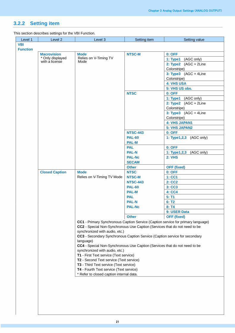
3.2.2 Setting item
This section describes settings for the VBI Function.
Level 1 Level 2 Level 3 Setting item Setting value
VBI
Function
Macrovision * Only displayed with a license
Mode Relies on V-Timing TV Mode
NTSC-M 0: OFF
1: Type1 (AGC only)
2: Type2 (AGC + 2Line
Colorstripe)
3: Type3 (AGC + 4Line
Colorstripe)
4: VHS USA
5: VHS US obs.
NTSC 0: OFF
1: Type1 (AGC only)
2: Type2 (AGC + 2Line
Colorstripe)
3: Type3 (AGC + 4Line
Colorstripe)
4: VHS JAPAN1
5: VHS JAPAN2
NTSC-443 0: OFF
PAL-60 1: Type1,2,3 (AGC only)
PAL-M
PAL 0: OFF
PAL-N 1: Type1,2,3 (AGC only)
PAL-Nc 2: VHS
SECAM
Other OFF (fixed)
Closed Caption Mode
Relies on V-Timing TV Mode
NTSC 0: OFF
NTSC-M 1: CC1
NTSC-443 2: CC2
PAL-60 3: CC3
PAL-M 4: CC4
PAL 5: T1
PAL-N 6: T2
PAL-Nc 8: T4
9: USER Data
Other OFF (fixed)
CC1 - Primary Synchronous Caption Service (Caption service for primary language)
CC2 - Special Non-Synchronous Use Caption (Services that do not need to be
synchronized with audio, etc.)
CC3 - Secondary Synchronous Caption Service (Caption service for secondary
language)
CC4 - Special Non-Synchronous Use Caption (Services that do not need to be
synchronized with audio, etc.)
T1 - First Text service (Text service)
T2 - Second Text service (Text service)
T3 - Third Text service (Text service)
T4 - Fourth Text service (Text service)
* Refer to closed caption internal data.

Chapter 3 Analog Output Settings (ANALOG OUTPUT)
22
Level 1 Level 2 Level 3 Setting item Setting value
● Data included in closed captions
VBI
Function
Service Caption style, lines, colors, optional settings,
etc.
Characters
1 to CC4 Service
Roll-up2 ROW2 Background: Black, opaque Text: White
Primary Synchronous Caption Service -- CC1 (CC1) Secondary Synchronous Caption Service -- CC2 (CC2) Special Non-Synchronous Use Captions -- CC3 (CC3) Special Non-Synchronous Use Captions -- CC4 (CC4)
Roll-up3 ROW10 Background: Blue, opaque Text: Yellow
Roll-up Style Characters are always displayed immediately. Each time a Carriage Return is received,
The text is scrolled up one row. Roll-up4 ROW15, indent Background: Cyan, opaque Text: Red
Standard characters 0123456789 ABCDEFGHIJ áàâçéèêíîÑñóôúû !,.;:7”#% &@/() []+-÷<=>? Music note, solid block, Transparent space, solid block, Music note, solid block, Transparent space
Pop-on ROW1 ROW2 ROW3 Background: Red, semitransparent Text: Cyan
Pop-on Style Caption data are loaded into a non-displayed memory.
Pop-on ROW4 ROW5 ROW6 Background: Green, semitransparent Text: Blue, flash
End of Caption command (EOC) “flips” displayed and non displayed memory.
Pop-on ROW7 indent ROW8 indent ROW9 indent Background: Magenta, opaque Text: Green, italic
ABCDEFGHIJ 0123456789 Å å Ø ø┌┐└┘
Pop-on ROW12 indent ROW13 indent ROW14 indent ROW15 indent Background: White, opaque Text: Red, underlined
ÁÉÓÚÜü, opening single quote, inverted exclamation mark ÀÂÇÈÊËëÎÏïÔÙùÛ«» ÃãÍÌìÒòÕõ{}\^_|~ ÄäÖöß\¤|
Paint-on ROW1 ROW3 ROW4 ROW6 ROW7 ROW9 Background: Yellow, semitransparent Text: Blue
Paint-on Style Characters are always displayed immediately. Characters on next row will be erased by Backspace. ABCDEFGH (A to H is deleted by Backspace)

Chapter 3 Analog Output Settings (ANALOG OUTPUT)
23
Level 1 Level 2 Level 3 Setting item Setting value
VBI
Function
Paint-on ROW5 ROW6 ROW7 ROW8 ROW9 ROW10 ROW12, indent ROW14, indent Background: Yellow, semitransparent Text: Blue
Once the cursor reaches the 32nd column position on any row, all subsequent characters will be displayed In that column replacing any previous character. ABCDEFGHIJKLMNOPQRSTUVWXYZ (S to Y are replaced by Z) Abcdefghijklmnopqrstuvwxyz (n to y are replaced by z)
T1 -- First Text Service -- T1 Text Mode is a data service, generally not program related, which may be transmitted using either field of line21. Text Mode data are always displayed as soon as they are received and are intended to be displayed in a manner which isolates them from the video program used to transmit the data. Once the display window is filled these data are always scrolled upward through the display window provided by the decoder.
T2 -- Second Text Service -- T2 ABCDEFGHIJKLMNOPQRSTUVWXYZ abcdefghijklmnopqrstuvwxyz 012345678901234567890 !”#$%&'()á+,-./ :;<=>?@[é]íóú *.–©SM•‟”\
T3 -- Third Text Service -- T3 A Text Mode may be used that consists of data formatted to fill a box which in height is not less than 7 rows and not more than 15 rows (all of which should be contiguous), and in width is not less than 32 columns. Text should be displayed over a solid background to isolate it from the unrelated program video. Each row of text contains maximum of 32 characters.
T4 -- Fourth Text Service -- T4 ABCDEFGHIJKLMNOPQRSTUVWXYZ abcdefghijklmnopqrstuvwxyz 012345678901234567890 !”#$%&'()á+,-./ :;<=>?@[é]íóú *.–©SM•‟”\
Closed Caption Interval 0 to 60 [s]
USER Data No.
* Only displayed when
Mode=USER Data is selected.
1 to 20
V-Chip System Relies on V-Timing TV Mode
NTSC 0: OFF
NTSC-M 1: MPAA
NTSC-443 2: U.S.TV
PAL-60 3: English
PAL-M 4: French
PAL
PAL-N
PAL-Nc
Other OFF (fixed)

Chapter 3 Analog Output Settings (ANALOG OUTPUT)
24
Level 1 Level 2 Level 3 Setting item Setting value
VBI
Function
V-Chip MPAA: Motion Picture Association of America
This organization was established in order to popularize American movies. The MPAA is
involved in a variety of activities including bolstering movie export to overseas markets
and regulating pirated movies. Also, self-imposed restrictions are established regarding
the depiction of violence, sex, and discrimination within the United States. Rating
standards are strict, with even the most minor of images and words that are not of
concern in Japan subject to review.
U.S.TV: U.S. TV Parental Guideline Rating System
This is a rating system built into household TVs in the United States.
English: Canadian English Language Rating System
This is a Canadian English language rating system.
French: Canadian French Language Rating System
This is a Canadian French language rating system.
MPAA 0: G
1: PG
2: PG-13
3: R
4: NC-17
5: X
6: Not Rated
7: N/A
G: General Audience All ages admitted.
PG: Parental Guidance Some material may not be suitable for children.
PG-13: Parents Strongly Cautioned Some material may be inappropriate for children
under 13.
R: Restricted Under 17 requires accompanying parent or adult guardian.
NC-17: No One 17 and Under Admitted No One 17 and Under Admitted.
X: Adult Movie For adults only.
Not Rated Not Submitted For MPAA Review
N/A No restrictions.
USTV 0: TV-Y
1: TV-Y7
2: TV-G
3: TV-PG
4: TV-14
5: TV-MA
6: Not Rated 1
7: Not Rated 2
TV-Y: All children This program is designed to be appropriate for all children.
TV-Y7: Directed to older children This program is designed for children age 7 and
above.
TV-G: General Audience Most parents would find this program suitable for all ages
(contains no violence, strong language, or sexual situations).
TV-PG: Parental Guidance Suggested The program contains material that parents
may find unsuitable for younger children, including a moderate amount of violence,
sexual content and scenes that could induce them to use rough language or act
inappropriately.
TV-14: Parents Strongly Cautioned This program contains material that many parents
would find unsuitable for children under 14 years of age, including violence, sexual
content and scenes that could induce them to use rough language or act inappropriately.
TV-MA: Mature Audience Only This program is specifically designed to be viewed by
adults, and is generally not broadcast.
Not Rated1/2 No restrictions.

Chapter 3 Analog Output Settings (ANALOG OUTPUT)
25
Level 1 Level 2 Level 3 Setting item Setting value
VBI
Function
V-Chip USTV Extension OFF/ON FV/V/S/L/D
Each bit 0: OFF / 1: ON ・ Editable bits depend on USTV.
TV-Y7: F,V
TV-PG,TV-14: V,S,L,D
TV-MA: V,S,L
Other None
English 0: E / 1: C / 2: C8+ / 3: G / 4: PG /
5: 14+ / 6: 18+
E: Exempt No age restrictions.
C: Children Content suitable for children of all ages.
C8+: Children eight years and older Content suitable for children 8 years of age and
older.
G: General Programming, suitable for all audiences Content suitable for general
audiences.
PG: Parental Guidance Content that can be viewed with parental permission.
14+: Viewers 14 years and older Content suitable for children 14 years of age and
older.
18+: Adult Programming Programming for viewers 18 years of age and older.
French 0: E / 1: G / 2: 8ans+ / 3: 13ans+ /
4: 16ans+ / 5: 18ans+
E: Exempt No age restrictions.
G: General Content suitable for general audiences.
8ans+: Not recommended for young children Content not suitable for young children.
13ans+: Programming may not be suitable for children under 13
Content not suitable for children under 13 years of age.
16ans+: Programming is not suitable for children under 16
Content not suitable for children under 16 years of age.
18ans+: Programming restricted to adults
Programming for viewers 18 years of age and older.
Interval 0 to 60 [s]
Teletext Mode: Relies on V-Timing TV Mode
PAL 0: OFF / 1: Default / 2: Page
Select
Other OFF (fixed)
Page This product can register up to 20 pages of teletext screens. Internal data numbers are set for each page.
Page data can be set from
100 to 899.
1: to 20: 100 to 899
* Refer to teletext default page list.
Line 8,321: 0: Disable / 1: Enable
Sets the line to output
teletext data.
Numbers indicate the
number of lines for the 1st
and 2nd fields.
9,322
10,323
11,324
12,325
13,326
14,327
15,328
16,329
17,330
18,331
19,332
20,333
21,334
22,335

Chapter 3 Analog Output Settings (ANALOG OUTPUT)
26
Level 1 Level 2 Level 3 Setting item Setting value
VBI
Function
● Teletext default page list
Page
No. Details Screen
Page
No. Details Screen
100 Index
Page
101 Test Page
Including FLASH and CONCEAL
102 Newsflash
103 Subtitle
200 Character
(English)
201 Character
(German)
202
Character
(Swedish/
Finnish/
Hungarian)
203 Character
(Italian)
204 Character
(French)
205
Character
(Portuguese/
Spanish)

Chapter 3 Analog Output Settings (ANALOG OUTPUT)
27
Level 1 Level 2 Level 3 Setting item Setting value
VBI
Function
206
Character
(Czech
/Slovak)
301 Colors
302 White Flat
505 Clock
Cracker
515 Multi Page
4 sub page
555 Test
Pattern1
560 Test
Pattern2
- Other
pages
For 700 pages
WSS OFF/ON Relies on V-Timing TV Mode
PAL 0: OFF / 1: ON
PAL-N
PAL-Nc
SECAM
Other OFF (fixed)
Aspect Ratio 0: Full Format 4:3
1: LB 14:9 center
2: LB 14:9 top
3: LB 16:9 center
4: LB 16:9 top
5: LB >16:9 center
6: Full Format 14:9
7: Full Format 16:9

Chapter 3 Analog Output Settings (ANALOG OUTPUT)
28
Level 1 Level 2 Level 3 Setting item Setting value
VBI
Function
CGMS-A/ID-1 OFF/ON Field1 (Sets line
20 output for 1st field)
Field2 (Sets line 283 output
for 2nd field) Relies on V-Timing TV Mode
NTSC 0: OFF / 1: ON
NTSC-M
NTSC-443
PAL-60
PAL-M
Other OFF (fixed)
Aspect 0: 4:3 Normal
1: 16:9 Normal
2: 4:3 Letter Box
3: Not Defined
CGMS-A 0: Copying Permitted
Enables copying.
1: Not Used Condition
Sets undefined condition.
2: Copy Once
Enables copying once.
3: No Copying Permitted
Disables copying.

Chapter 4 Digital Output Settings (DIGITAL OUTPUT)
29
Chapter 4 Digital Output Settings (DIGITAL OUTPUT)
4.1 HDMI unit functions and settings
The applicable unit is as follows.
4.1.1 HDMI unit VM-1876-M0 and VM-1876A-M0
● Unit exterior diagram
No. Name Description
① COAX digital audio output Outputs audio to the selected Port when HDMI 1, 2, 3, 4 ARC signal is received.
② HDMI 1
This is HDMI digital video/audio output terminal 1 to 4. (Supports HDCP) ③ HDMI 2
④ HDMI 3
⑤ HDMI 4
⑥ Standby LED Lights when output preparation is complete. On: Normal
Off: Error (module damaged, wrong slot, etc.)
① ② ③ ④ ⑤ ⑥

Chapter 4 Digital Output Settings (DIGITAL OUTPUT)
30
● Specifications
HDMI
CH1
CH2
CH3
CH4
Connector HDMI x4
Dot clock
*4
Single clock mode
<For RGB/YCbCr444>
8 bit: 25 to 300 MHz
10 bit: 25 to 240 MHz
12 bit: 25 to 200 MHz
16 bit: 25 to 150 MHz
<For YCbCr422>
8 bit: 25 to 300 MHz
10 bit: 25 to 300 MHz
12 bit: 25 to 300 MHz
Dual clock mode
*1
<For RGB/YCbCr444>
8 bit: 50 to 600 MHz
10 bit: 50 to 480 MHz
12 bit: 50 to 400 MHz
16 bit: 50 to 300 MHz
<For YCbCr422>
8 bit: 50 to 600 MHz
10 bit: 50 to 600 MHz
12 bit: 50 to 600 MHz
<For YCbCr420>
8 bit: 50 to 600 MHz
10 bit: 50 to 480 MHz
12 bit: 50 to 400 MHz
16 bit: 50 to 300 MHz
Quad clock mode
*2
<For RGB/YCbCr444>
8 bit: 100 to 1200 MHz
10 bit: 100 to 960 MHz
12 bit: 100 to 800 MHz
16 bit: 100 to 600 MHz
<For RGB/YCbCr422>
8 bit: 100 to 1200 MHz
10 bit: 100 to 1200 MHz
12 bit: 100 to 1200 MHz
No. of colors RGB 8/10/12/16bit each (RGB/ YCbCr444/ YCbCr422/ YCbCr420
compatible)
Audio
Output
HDMI
L-PCM
Sampling: 32k / 44.1k / 48k / 88.2k / 96k / 176.4k / 192 kHz
Output frequency: 100 to 20 kHz
No. of bits: 16 / 20 / 24bit
Compression AC3, AAC
Option
Next-generation audio compatible*3
DSD, Dolby Digital Plus, Dolby True HD,
DTS HD (High Resolution Audio), DTS HD (Master Audio) etc.
COAX Sampling: 32k / 44.1k / 48k / 88.2k / 96k / 176.4k / 192 kHz
Copy protect HDCP Ver1.4
Added functions E-EDID Ver1.4 (DDC2B), xvYCC, CEC
*1 Uses CH1-CH2 (CH3-CH4) for parallel output. However, distributes output for YCbCr420 only.
*2 Uses CH1-CH2-CH3-CH4 for parallel output.
*3 Next-generation audio function is available when a license is purchased.
*4 TMDSCLK 3GHz

Chapter 4 Digital Output Settings (DIGITAL OUTPUT)
31
4.1.2 HDMI 6G Unit VM-1876-M6, VM-1876A-M6
● Unit exterior diagram
No. Name Description
① COAX digital audio output Outputs audio to the selected Port when HDMI 1 or 2 ARC signal is received.
② HDMI 1 This is HDMI digital video/audio output terminal 1. (Supports HDCP)
③ HDMI 2 This is HDMI digital video/audio output terminal 2. (Supports HDCP)
④ Standby LED Lights when output preparation is complete. On: Normal
Off: Error (module damaged, wrong slot, etc.)
● When data transfer speed (TMDS clock) output is 3G or below, Timing edited in Timing editing can be output, however,
Timing output that exceeds 3G will be output from CEA-861-F standard Video Identification Code (VIC) 93 to107 Timing
only.
(Output of edited Timing that exceeds 3G is not available.)
Additionally, VIC91 and VIC92 Timing output is not available.
VIC91 : 2560x1080p Field Rate100Hz Pixel Frequency 371.25 MHz
VIC92 : 2560x1080p Field Rate119.88/120 Hz Pixel Frequency 495 MHz
● Deep Color output for Timing that exceeds 3G uses 8-bit display gradation for output color format YCbCr 4:2:0, and 12-
bit display gradation for RGB and YCbCr4:4:4 16bit. (Low-level bits are output with 0 fill-in for Deep Color.)
● 3D display for Timing that exceeds 3G is only compatible with Top and Bottom and Side By Side (Half).
(TMDS clock calculation method)
Output color format coefficient
RGB=1.0, YCbCr4:4:4=1.0, YCbCr4:2:2=0.666(2/3) ,YCbCr4:2:0=0.5(1/2)
Output bit coefficient
8 bits = 1.0, 10 bits = 1.25, 12 bits = 1.5, 16 bits = 2.0
TMDS clock = dot clock x output color format coefficient x output bit coefficient
Ex. Dot clock: 148.5 MHz (1.485G)
Output color format: YCbCr4:2:2 (output color format coefficient 0.666(2/3))
Output bit coefficient: 10 bits (output bit coefficient 1.25)
TMDS clock = 1.485G x 0.666 (2/3) x 1.25
TMDS clock = 1.2375G
① ② ③
④

Chapter 4 Digital Output Settings (DIGITAL OUTPUT)
32
● Specifications
HDMI
CH1
CH2
Connector HDMI x2
Dot clock
*1
Single clock mode
<For RGB/YCbCr444>
8bit: 25 to 300 MHz
10bit: 25 to 240 MHz
12bit: 25 to 200 MHz
16bit: 25 to 150 MHz
<For YCbCr422>
8 / 10 / 12 bit: 25 to 300 MHz
Dual clock mode
*2
<For RGB/YCbCr444>
8bit: 597 MHz
<For YCbCr422>
12bit: 597 MHz
<For YCbCr420>
8bit: 50 to 600 MHz
10bit: 50 to 480 MHz
12bit: 50 to 400 MHz
16bit: 50 to 300 MHz
No. of colors
*3*4
RGB 8 / 10 / 12bit / 16bit each
(RGB / YCbCr444 / YCbCr422 / YCbCr420 compatible)
Audio
Output
HDMI
L-PCM
Sampling: 32k / 44.1k / 48k / 88.2k / 96k / 176.4k / 192k
Output frequency: 100 to 20 kHz
No. of bits: 16 / 20 / 24bit
Compression AC3, AAC
Option
Next-generation audio compatible*5
DSD, Dolby Digital Plus, Dolby Ture HD,
DTS HD (High Resolution Audio), DTS HD (Master Audio) etc.
COAX Sampling: 32k / 44.1k / 48k / 88.2k / 96k / 176.4k / 192k
Copy protect HDCP Ver1.4
Added functions E-EDID Ver1.4 (DDC2B), xvYCC, CEC
*1 Quad clock mode is not supported.
*2 The same data is constantly output from CH1 and CH2 (distributed output). Distributed output is not supported.
*3 Up to 8-bit gradation is available for YCbCr4:2:0.
*4 Up to 12-bit gradation is available for 4K output.
*5 Next-generation audio function is available when a license is purchased.

Chapter 4 Digital Output Settings (DIGITAL OUTPUT)
33
4.1.3 HDMI HDCP2.2 Unit VM-1876-M7
● Unit exterior diagram
No. Name Description
① HDMI 1
This is HDMI digital video/audio output terminal 1 to 4. (Supports HDCP) ② HDMI 2
③ HDMI 3
④ HDMI 4
⑤ Standby LED Lights when output preparation is complete. On: Normal
Off: Error (module damaged, wrong slot, etc.)
[Compatible Formats]
2D Video Resolution Pixel Format Color Depth
(bits per pixel)
Maximum
Frame Rate
(Hz)
VGA RGB 24 60
WVGA RGB 24 60
SVGA RGB 24 60
XGA RGB 24 60
UXGA RGB 24 60
WUXGA RGB 24 60
QXGA RGB 24 60
WQXGA RGB 24 60
480p/i RGB
YCbCr 4:4:4
24, 36 60
YCbCr 4:2:2 16, 24
576p/i RGB
YCbCr 4:4:4
24, 36 50
YCbCr 4:2:2 16, 24
720p RGB
YCbCr 4:4:4
24, 36 50/60
YCbCr 4:2:2 16, 24
1080i RGB
YCbCr 4:4:4
24, 36 50/60
YCbCr 4:2:2 16, 24
1080p RGB
YCbCr 4:4:4
24, 36 50/60
YCbCr 4:2:2 16, 24
4K x 2K RGB
YCbCr 4:4:4
24, 36 24/25/30
YCbCr 4:2:2 16, 24
YCbCr 4:2:0 12 50/60
① ② ③ ④ ⑤

Chapter 4 Digital Output Settings (DIGITAL OUTPUT)
34
● Specifications
HDMI
CH1
CH2
CH3
CH4
Connector HDMI x4
Dot clock
*4
Single clock mode
<For RGB/YCbCr444>
8 bit: 25 to 300 MHz
10 bit: 25 to 240 MHz
12 bit: 25 to 200 MHz
<For YCbCr422>
8 / 10 / 12 bit: 25 to 300 MHz
Dual clock mode
*1
<For RGB/YCbCr444>
8 bit: 50 to 600 MHz
10 bit: 50 to 480 MHz
12 bit: 50 to 400 MHz
<For YCbCr422>
8 / 10 /12 bit: 50 to 600 MHz
<For YCbCr420>
8 bit: 50 to 600 MHz
10 bit: 50 to 480 MHz
12 bit: 50 to 400 MHz
Quad clock mode
*2
<For RGB/YCbCr444>
8 bit: 100 to 1200 MHz
10 bit: 100 to 960 MHz
12 bit: 100 to 800 MHz
<For RGB/YCbCr422>
8 / 10 / 12 bit: 100 to 1200 MHz
No. of colors RGB 8/10/12 bit each (RGB/ YCbCr444/ YCbCr422/ YCbCr420 (8-bit only
compatible))
Audio
Output
HDMI
L-PCM
Sampling: 32k / 44.1k / 48k / 88.2k / 96k / 176.4k / 192 kHz
Output frequency: 100 to 20 kHz
No. of bits: 16 / 20 / 24bit
Compression AC3, AAC
Option
Next-generation audio compatible*3
DSD, Dolby Digital Plus, Dolby True HD,
DTS HD (High Resolution Audio), DTS HD (Master Audio) etc.
COAX Sampling: 32k / 44.1k / 48k / 88.2k / 96k / 176.4k / 192 kHz
Copy protect HDCP Ver2.2 or Ver1.4 (relies on Sink)
Added functions E-EDID Ver1.4 (DDC2B), xvYCC, CEC
*1 Uses CH1-CH2 (CH3-CH4) for parallel output. However, distributes output for YCbCr420 only.
*2 Uses CH1-CH2-CH3-CH4 for parallel output.
*3 Next-generation audio function is available when a license is purchased.
*4 TMDSCLK 3GHz

Chapter 4 Digital Output Settings (DIGITAL OUTPUT)
35
4.1.4 HDMI 6G HDCP2.2 Unit VM-1876-M8
● Unit exterior diagram
No. Name Description
① HDMI 1 This is HDMI digital video/audio output terminal 1. (Supports HDCP)
② HDMI 2 This is HDMI digital video/audio output terminal 2. (Supports HDCP)
③ Standby LED Lights when output preparation is complete. On: Normal
Off: Error (module damaged, wrong slot, etc.)
● Data transfer speed (TMDS clock) is CEA-861-F standard Video Identification Code
Only (VIC) VIC1 to 90, 93 to 108, and the following VESA compatible format Timing are available for output.
● 3D display is only compatible with Top and Bottom and Side By Side (Half).
[VESA Compatible Formats]
PrgNo Program Name PrgNo Program Name PrgNo Program Name
1602 VESA640x400@85 1628 VESA1280x800@60 1652 VESA1600x1200@65
1603 VESA720x400@85 1629 VESA1280x800@75 1653 VESA1600x1200@70
1604 VESA640x480@60 1630 VESA1280x800@85 1654 VESA1600x1200@75
1605 VESA640x480@72 1631 VESA1280x800@120CVT 1655 VESA1600x1200@85
1606 VESA640x480@75 1632 VESA1280x960@60 1656 VESA1600x1200@120CVT
1607 VESA640x480@85 1633 VESA1280x960@85 1657 VESA1680x1050@60CVT
1608 VESA800x600@56 1634 VESA1280x960@120CVT 1658 VESA1680x1050@60
1609 VESA800x600@60 1635 VESA1280x1024@60 1659 VESA1680x1050@75
1610 VESA800x600@72 1636 VESA1280x1024@75 1660 VESA1680x1050@85
1611 VESA800x600@75 1637 VESA1280x1024@85 1661 VESA1680x1050@120CVT
1612 VESA800x600@85 1638 VESA1280x1024@120CVT 1668 VESA1920x1200@60CVT
1613 VESA800x600@120CVT 1639 VESA1360x768@60 1669 VESA1920x1200@60
1614 VESA848x480@60 1640 VESA1360x768@120CVT 1670 VESA1920x1200@75
1615 VESA1024x768@43 1641 VESA1400x1050@60CVT 1671 VESA1920x1200@85
1616 VESA1024x768@60 1642 VESA1400x1050@60
1617 VESA1024x768@70 1643 VESA1400x1050@75
1618 VESA1024x768@75 1644 VESA1400x1050@85
1619 VESA1024x768@85 1645 VESA1400x1050@120CVT
1620 VESA1024x768@120CVT 1646 VESA1440x900@60CVT
1622 VESA1280x768@60CVT 1647 VESA1440x900@60
1623 VESA1280x768@60 1648 VESA1440x900@75
1624 VESA1280x768@75 1649 VESA1440x900@85
1625 VESA1280x768@85 1650 VESA1440x900@120CVT
1627 VESA1280x800@60CVT 1651 VESA1600x1200@60
① ②
③

Chapter 4 Digital Output Settings (DIGITAL OUTPUT)
36
● Specifications
HDMI
CH1
CH2
Connector HDMI x2
Dot clock
*1
Single clock mode
<For RGB/YCbCr444>
8bit: 25 to 300 MHz
10bit: 25 to 240 MHz
12bit: 25 to 200 MHz
16bit: 25 to 150 MHz
<For YCbCr422>
8 / 10 / 12 bit: 25 to 300 MHz
Dual clock mode
*2
<For RGB/YCbCr444>
8bit: 597 MHz
<For YCbCr422>
12bit: 597 MHz
<For YCbCr420>
8bit: 50 to 600 MHz
10bit: 50 to 480 MHz
12bit: 50 to 400 MHz
16bit: 50 to 300 MHz
No. of colors
*3*4
RGB 8 / 10 / 12bit / 16bit each
(RGB / YCbCr444 / YCbCr422 / YCbCr420 compatible)
Audio
Output
HDMI
L-PCM
Sampling: 32k / 44.1k / 48k / 88.2k / 96k / 176.4k / 192k
Output frequency: 100 to 20 kHz
No. of bits: 16 / 20 / 24bit
Compression AC3, AAC
Option
Next-generation audio compatible*5
DSD, Dolby Digital Plus, Dolby Ture HD,
DTS HD (High Resolution Audio), DTS HD (Master Audio) etc.
COAX Sampling: 32k / 44.1k / 48k / 88.2k / 96k / 176.4k / 192k
Copy protect HDCP Ver2.2 or Ver1.4
Added functions E-EDID Ver1.4 (DDC2B), xvYCC, CEC
*1 Quad clock mode is not supported.
*2 The same data is constantly output from CH1 and CH2 (distributed output). Distributed output is not supported.
*3 Up to 8-bit gradation is available for YCbCr4:2:0.
*4 Up to 12-bit gradation is available for 4K output.
*5 Next-generation audio function is available when a license is purchased.

Chapter 4 Digital Output Settings (DIGITAL OUTPUT)
37
4.1.5 HDMI 2.1 Unit VM-1876-MD
● Unit exterior diagram
No. Name Description
① COAX Digital Audio Output Outputs audio when receiving ARC and eARC signals in HDMI1.
② HDMI 1 This is HDMI digital video/audio output terminal 1. (Supports HDCP)
③ Standby LED Lights when output preparation is complete. On: Normal
Off: Error (module damaged, wrong slot, etc.)
● TMDS clock and FRL clock can only output Timing of the following formats.
● 3D is not supported.
[TMDS Support Format]
VIC Resolution V Frequency RGB YC444 YC422 YC420
1 640x480 60 8,10,12bit 8,10,12bit 12bit
2 720x480 60 8,10,12bit 8,10,12bit 12bit
3 720x480 60 8,10,12bit 8,10,12bit 12bit
4 1280x720 60 8,10,12bit 8,10,12bit 12bit
8 1440x240 60 8,10,12bit 8,10,12bit
9 1440x240 60 8,10,12bit 8,10,12bit
14 1440x480 60 8,10,12bit 8,10,12bit
15 1440x480 60 8,10,12bit 8,10,12bit
16 1920x1080 60 8,10,12bit 8,10,12bit 12bit
17 720x576 50 8,10,12bit 8,10,12bit 12bit
18 720x576 50 8,10,12bit 8,10,12bit 12bit
19 1280x720 50 8,10,12bit 8,10,12bit 12bit
29 1440x576 50 8,10,12bit 8,10,12bit
30 1440x576 50 8,10,12bit 8,10,12bit
31 1920x1080 50 8,10,12bit 8,10,12bit 12bit
32 1920x1080 24 8,10,12bit 8,10,12bit 12bit
33 1920x1080 25 8,10,12bit 8,10,12bit 12bit
34 1920x1080 30 8,10,12bit 8,10,12bit 12bit
41 1280x720 100 8,10,12bit 8,10,12bit 12bit
42 720x576 100 8,10,12bit 8,10,12bit 12bit
43 720x576 100 8,10,12bit 8,10,12bit 12bit
47 1280x720 120 8,10,12bit 8,10,12bit 12bit
48 720x480 120 8,10,12bit 8,10,12bit 12bit
49 720x480 120 8,10,12bit 8,10,12bit 12bit
52 720x576 200 8,10,12bit 8,10,12bit 12bit
53 720x576 200 8,10,12bit 8,10,12bit 12bit
56 720x480 240 8,10,12bit 8,10,12bit 12bit
57 720x480 240 8,10,12bit 8,10,12bit 12bit
① ② ③

Chapter 4 Digital Output Settings (DIGITAL OUTPUT)
38
VIC Resolution V Frequency RGB YC444 YC422 YC420
60 1280x720 24 8,10,12bit 8,10,12bit 12bit
61 1280x720 25 8,10,12bit 8,10,12bit 12bit
62 1280x720 30 8,10,12bit 8,10,12bit 12bit
63 1920x1080 120 8,10,12bit 8,10,12bit 12bit
64 1920x1080 100 8,10,12bit 8,10,12bit 12bit
65 1280x720 24 8,10,12bit 8,10,12bit 12bit
66 1280x720 25 8,10,12bit 8,10,12bit 12bit
67 1280x720 30 8,10,12bit 8,10,12bit 12bit
68 1280x720 50 8,10,12bit 8,10,12bit 12bit
69 1280x720 60 8,10,12bit 8,10,12bit 12bit
70 1280x720 100 8,10,12bit 8,10,12bit 12bit
71 1280x720 120 8,10,12bit 8,10,12bit 12bit
72 1920x1080 24 8,10,12bit 8,10,12bit 12bit
73 1920x1080 25 8,10,12bit 8,10,12bit 12bit
74 1920x1080 30 8,10,12bit 8,10,12bit 12bit
75 1920x1080 50 8,10,12bit 8,10,12bit 12bit
76 1920x1080 60 8,10,12bit 8,10,12bit 12bit
77 1920x1080 100 8,10,12bit 8,10,12bit 12bit
78 1920x1080 120 8,10,12bit 8,10,12bit 12bit
79 1680x720 24 8,10,12bit 8,10,12bit 12bit
80 1680x720 25 8,10,12bit 8,10,12bit 12bit
81 1680x720 30 8,10,12bit 8,10,12bit 12bit
82 1680x720 50 8,10,12bit 8,10,12bit 12bit
83 1680x720 60 8,10,12bit 8,10,12bit 12bit
84 1680x720 100 8,10,12bit 8,10,12bit 12bit
85 1680x720 120 8,10,12bit 8,10,12bit 12bit
86 2560x1080 24 8,10,12bit 8,10,12bit 12bit
87 2560x1080 25 8,10,12bit 8,10,12bit 12bit
89 2560x1080 50 8,10,12bit 8,10,12bit 12bit
90 2560x1080 60 8,10,12bit 8,10,12bit 12bit
93 3840x2160 24 8,10,12bit 8,10,12bit 12bit
94 3840x2160 25 8,10,12bit 8,10,12bit 12bit
95 3840x2160 30 8,10,12bit 8,10,12bit 12bit
96 3840x2160 50 8bit 8bit 12bit 8,10,12bit
97 3840x2160 60 8bit 8bit 12bit 8,10,12bit
98 4096x2160 24 8,10,12bit 8,10,12 12bit
99 4096x2160 25 8,10,12bit 8,10,12 12bit
100 4096x2160 30 8,10,12bit 8,10,12 12bit
101 4096x2160 50 8bit 8bit 12bit 8,10,12bit
102 4096x2160 60 8bit 8bit 12bit 8,10,12bit
103 3840x2160 24 8,10,12bit 8,10,12bit 12bit
104 3840x2160 25 8,10,12bit 8,10,12bit 12bit
105 3840x2160 30 8,10,12bit 8,10,12bit 12bit
106 3840x2160 50 8bit 8bit 12bit 8,10,12bit
107 3840x2160 60 8bit 8bit 12bit 8,10,12bit

Chapter 4 Digital Output Settings (DIGITAL OUTPUT)
39
[FRL Support Format]
VIC Resolution RGB/YCC Bit Rate (Gbps) Lane
199 198
8K60 8K50
420
8
8 4
10 4
12 4
10 10 4
12 4
12 12 4
196,203 195,204 117,119
218
8K30 8K25
4K100(3840) 4K100(4096)
420
8
6 3
6 4
8 4
10 4
12 4
10
6 4
8 4
10 4
12 4
12
6 4
8 4
10 4
12 4
422 12
8 4
10 4
12 4
444/RGB
8
8 4
10 4
12 4
10 10 4
12 4
12 12 4
194,202 8K24
420
8
6 3
6 4
8 4
10 4
12 4
10
6 4
8 4
10 4
12 4
12
6 4
8 4
10 4
12 4
422 12
8 4
10 4
12 4
444/RGB
8
8 4
10 4
12 4
10 10 4
12 4

Chapter 4 Digital Output Settings (DIGITAL OUTPUT)
40
VIC Resolution RGB/YCC Bit Rate (Gbps) Lane
118,120 4K120(3840)
420
8
6 3
6 4
8 4
10 4
12 4
10
6 4
8 4
10 4
12 4
12
8 4
10 4
12 4
422 12
8 4
10 4
12 4
444/RGB
8
8 4
10 4
12 4
10 10 4
12 4
12 12 4
219 4K120(4096)
420
8 10 4
12 4
10 10 4
12 4
12 10 4
12 4
422 12 10 4
12 4
444/RGB
8 10 4
12 4
10 12 4
12 12 4
96,106 97,107
101 102
4K50(3840) 4K60(3840) 4K50(4096) 4K60(4096)
420
8
3 3
6 3
6 4
8 4
10 4
12 4
10
6 3
6 4
8 4
10 4
12 4
12
6 3
6 4
8 4
10 4
12 4

Chapter 4 Digital Output Settings (DIGITAL OUTPUT)
41
VIC Resolution RGB/YCC Bit Rate (Gbps) Lane
96,106 97,107
101 102
4K50(3840) 4K60(3840) 4K50(4096) 4K60(4096)
422 12
6 3
6 4
8 4
10 4
12 4
444/RGB
8
6 3
6 4
8 4
10 4
12 4
10
6 4
8 4
10 4
12 4
12
6 4
8 4
10 4
12 4
93,103 94,104 95,105
98 99
100 63,78 64,77
4K24(3840) 4K25(3840) 4K30(3840) 4K24(4096) 4K25(4096) 4K30(4096) 1080p120 1080p100
422 12
3 3
6 3
6 4
8 4
10 4
12 4
444/RGB
8
3 3
6 3
6 4
8 4
10 4
12 4
10
6 3
6 4
8 4
10 4
12 4
12
6 3
6 4
8 4
10 4
12 4
16,76 34,74
72 1
1080p60 1080p30 1080p24
VGA
422 12
3 3
6 3
6 4
8 4
10 4
12 4
444/RGB 8,10,12
3 3
6 3
6 4
8 4
10 4
12 4

Chapter 4 Digital Output Settings (DIGITAL OUTPUT)
42
VIC Resolution RGB/YCC Bit Rate (Gbps) Lane
2 4
480p 720p
422 12
3 3
6 3
6 4
8 4
10 4
12 4
444/RGB 8,12
3 3
6 3
6 4
8 4
10 4
12 4
● Specifications
HDMI
CH1
Connector HDMI x 1ch
Dot Clock
TMDS Refer to [TMDS Support Format]
FRL Refer to [FRL Support Format]
Number of Colors
*1
RGB 8 / 10 / 12bit
(RGB / YCbCr444 / YCbCr422 / YCbCr420)
Audio
Output
HDMI
L-PCM
Sampling : 32k / 44.1k / 48k / 88.2k / 96k / 176.4k / 192k
Output Frequency: 100 to 20kHz
Bit: 16 / 20 / 24bit
Compressed AC3, AAC
Option Next generation audio *2
Dolby Digital Plus, DTS HD(High Resolution Audio)
COAX Sampling: 32k / 44.1k / 48k / 88.2k / 96k / 176.4k / 192k
Copy Protection HDCP Ver2.3 orVer1.4 *3
Additional Function E-EDID Ver1.4(DDC2B)、xvYCC、CEC
*1 The lower 2 bits of the 12 bit gradation are assigned by 0.
*2 Next generation audio is license option.
*3 When using FRL output, HDCP2.3 is only supported.
・ Set “ON” of “VM-1876-MD Mode” in 4.1.10 HDMI configuration setting items
・ If you output other VMs except VM-1876-MD, set “OFF” of “VM-1876-MD Mode”
・ If you set “ON” of “VM-1876-MD Mode”, other boards does not output signal.
・ When 8K timing is output, scroll is not supported.

Chapter 4 Digital Output Settings (DIGITAL OUTPUT)
43
4.1.6 Internal HDMI output section
● Unit exterior diagram
No. Name Description
① HDMI 1
This is HDMI digital video/audio output terminal 1 to 4. (Supports HDCP) ② HDMI 2
③ HDMI 3
④ HDMI 4
● Data transfer speed (TMDS clock) is CEA-861-F standard Video Identification Code
Only (VIC) VIC1 to 90, 93 to 108, and the following VESA compatible format Timing are available for output.
● 3D display is only compatible with Top and Bottom and Side By Side (Half).
[VESA Compatible Formats]
PrgNo Program Name PrgNo Program Name PrgNo Program Name
1602 VESA640x400@85 1628 VESA1280x800@60 1652 VESA1600x1200@65
1603 VESA720x400@85 1629 VESA1280x800@75 1653 VESA1600x1200@70
1604 VESA640x480@60 1630 VESA1280x800@85 1654 VESA1600x1200@75
1605 VESA640x480@72 1631 VESA1280x800@120CVT 1655 VESA1600x1200@85
1606 VESA640x480@75 1632 VESA1280x960@60 1656 VESA1600x1200@120CVT
1607 VESA640x480@85 1633 VESA1280x960@85 1657 VESA1680x1050@60CVT
1608 VESA800x600@56 1634 VESA1280x960@120CVT 1658 VESA1680x1050@60
1609 VESA800x600@60 1635 VESA1280x1024@60 1659 VESA1680x1050@75
1610 VESA800x600@72 1636 VESA1280x1024@75 1660 VESA1680x1050@85
1611 VESA800x600@75 1637 VESA1280x1024@85 1661 VESA1680x1050@120CVT
1612 VESA800x600@85 1638 VESA1280x1024@120CVT 1668 VESA1920x1200@60CVT
1613 VESA800x600@120CVT 1639 VESA1360x768@60 1669 VESA1920x1200@60
1614 VESA848x480@60 1640 VESA1360x768@120CVT 1670 VESA1920x1200@75
1615 VESA1024x768@43 1641 VESA1400x1050@60CVT 1671 VESA1920x1200@85
1616 VESA1024x768@60 1642 VESA1400x1050@60
1617 VESA1024x768@70 1643 VESA1400x1050@75
1618 VESA1024x768@75 1644 VESA1400x1050@85
1619 VESA1024x768@85 1645 VESA1400x1050@120CVT
1620 VESA1024x768@120CVT 1646 VESA1440x900@60CVT
1622 VESA1280x768@60CVT 1647 VESA1440x900@60
1623 VESA1280x768@60 1648 VESA1440x900@75
1624 VESA1280x768@75 1649 VESA1440x900@85
1625 VESA1280x768@85 1650 VESA1440x900@120CVT
1627 VESA1280x800@60CVT 1651 VESA1600x1200@60
① ② ③ ④

Chapter 4 Digital Output Settings (DIGITAL OUTPUT)
44
● Specifications
HDMI
CH1
CH2
CH3
CH4
Connector HDMI x2
Dot clock
*1
Single clock mode
<For RGB/YCbCr444>
8bit: 25 to 300 MHz
10bit: 25 to 240 MHz
12bit: 25 to 200 MHz
16bit: 25 to 150 MHz
<For YCbCr422>
8 / 10 / 12 bit: 25 to 300 MHz
Dual clock mode
*2
<For RGB/YCbCr444>
8bit: 597 MHz
<For YCbCr422>
12bit: 597 MHz
<For YCbCr420>
8bit: 50 to 600 MHz
10bit: 50 to 480 MHz
12bit: 50 to 400 MHz
16bit: 50 to 300 MHz
No. of colors
*3*4
RGB 8 / 10 / 12bit / 16bit each
(RGB / YCbCr444 / YCbCr422 / YCbCr420 compatible)
Audio
Output HDMI L-PCM
Sampling: 32k / 44.1k / 48k / 88.2k / 96k / 176.4k / 192k
Output frequency: 100 to 20 kHz
No. of bits: 16 / 20 / 24bit
Copy protect HDCP Ver2.2 or Ver1.4
Added functions E-EDID Ver1.4 (DDC2B), xvYCC, CEC
*1 Quad clock mode is not supported.
*2 The same data is constantly output from CH1 and CH2 (distributed output). Distributed output is not supported.
*3 Up to 8-bit gradation is available for YCbCr4:2:0.
*4 Up to 12-bit gradation is available for 4K output.
*5 The next generation audio is an option.

Chapter 4 Digital Output Settings (DIGITAL OUTPUT)
45
4.1.7 Connector and pin assignment
● Connector: HDMI Type A
Pin No. Signal
1 TMDS DATA2+
2 TMDS DATA2 SHIELD
3 TMDS DATA2-
4 TMDS DATA1+
5 TMDS DATA1 SHIELD
6 TMDS DATA1-
7 TMDS DATA0+
8 TMDS DATA0 SHIELD
9 TMDS DATA0-
10 TMDS CLK+
11 TMDS CLK SHIELD
12 TMDS CLK-
13 CEC
14 RESERVE/HEAC+
15 DDC CLK
16 DDC DATA
17 GROUND (for +5V)
18 +5 V (DDC power supply*1)
19 HOT PLUG DETECT/HEAC-
Shell FG
*1 The supply current of the DDC power supply is limited. For details, refer to “5.1 DDC power supply max power current
consumption”.

Chapter 4 Digital Output Settings (DIGITAL OUTPUT)
46
4.1.8 HDMI data transfer method
This section describes the data transfer method output from the HDMI unit.
Transfer method differs according to the dot clock operation mode (DotClk Mode).
For details on how to set the dot clock operation mode (DotClk Mode), refer to “Dot clock operation mode DotClk Mode settings”
in the instruction manual of the corresponding VG unit.
● 《When single clock mode》
This mode outputs via 1 HDMI connectors. The following
diagram shows video specifications and how data is
transferred.
Data transfer method
Screen panes
● 《Dual clock mode / Mode0, Mode2 (for 2 horizontal panes)》
This mode outputs via 2 HDMI connectors. The following
diagram shows video specifications and how data is
transferred.
Data transfer method
Screen panes
Pixel(0,0)
B(0,0)
G(0,0)
TMDSChannel
0
1
2 R(0,0)
Pixel(1,0)
R(1,0)
G(1,0)
B(1,0)
Pixel(2,0)
R(2,0)
G(2,0)
B(2,0)
Pixel(3837,2159)
B(3837,2159)
G(3837,2159)
R(3837,2159)
Pixel(3838,2159)
R(3838,2159)
G(3838,2159)
B(3838,2159)
Pixel(3839,2159)
R(3839,2159)
G(3839,2159)
B(3839,2159)
・・・・
・・・・
・・・・
・・・・
TMDSChannel
0
1
2
HDMICH1
HDMICH2
TMDSChannel
0
1
2
HDMICH3
TMDSChannel
0
1
2
HDMICH4
Pixel(0,0)
B(0,0)
G(0,0)
R(0,0)
Pixel(1,0)
R(1,0)
G(1,0)
B(1,0)
Pixel(2,0)
R(2,0)
G(2,0)
B(2,0)
Pixel(3837,2159)
B(3837,2159)
G(3837,2159)
R(3837,2159)
Pixel(3838,2159)
R(3838,2159)
G(3838,2159)
B(3838,2159)
Pixel(3839,2159)
R(3839,2159)
G(3839,2159)
B(3839,2159)
・・・・
・・・・
・・・・
・・・・
Pixel(0,0)
B(0,0)
G(0,0)
R(0,0)
Pixel(1,0)
R(1,0)
G(1,0)
B(1,0)
Pixel(2,0)
R(2,0)
G(2,0)
B(2,0)
Pixel(3837,2159)
B(3837,2159)
G(3837,2159)
R(3837,2159)
Pixel(3838,2159)
R(3838,2159)
G(3838,2159)
B(3838,2159)
Pixel(3839,2159)
R(3839,2159)
G(3839,2159)
B(3839,2159)
・・・・
・・・・
・・・・
・・・・
Pixel(0,0)
B(0,0)
G(0,0)
R(0,0)
Pixel(1,0)
R(1,0)
G(1,0)
B(1,0)
Pixel(2,0)
R(2,0)
G(2,0)
B(2,0)
Pixel(3837,2159)
B(3837,2159)
G(3837,2159)
R(3837,2159)
Pixel(3838,2159)
R(3838,2159)
G(3838,2159)
B(3838,2159)
Pixel(3839,2159)
R(3839,2159)
G(3839,2159)
B(3839,2159)
・・・・
・・・・
・・・・
・・・・
と同一HDMICH1
と同一HDMICH1
と同一HDMICH1
Pixel(0,0)
Pixel(3839,2159)
Pixel(3839,0)
Pixel(0,2159)
CH1
Pixel(0,0)
B(0,0)
G(0,0)
TMDSChannel
0
1
2 R(0,0)
Pixel(1,0)
R(1,0)
G(1,0)
B(1,0)
Pixel(2,0)
R(2,0)
G(2,0)
B(2,0)
・・・・
・・・・
・・・・
・・・・
TMDSChannel
0
1
2
Pixel(3837,1079)
B(3837,1079)
G(3837,1079)
R(3837,1079)
Pixel(3838,1079)
R(3838,1079)
G(3838,1079)
B(3838,1079)
Pixel(3839,1079)
R(3839,1079)
G(3839,1079)
B(3839,1079)
・・・・
・・・・
・・・・
・・・・
TMDSChannel
0
1
2
TMDSChannel
0
1
2
Pixel(3837,2159)
B(3837,2159)
G(3837,2159)
R(3837,2159)
Pixel(3838,2159)
R(3838,2159)
G(3838,2159)
B(3838,2159)
Pixel(3839,2159)
R(3839,2159)
G(3839,2159)
B(3839,2159)
Pixel(0,1080)
B(0,1080)
G(0,1080)
R(0,1080)
Pixel(1,1080)
R(1,1080)
G(1,1080)
B(1,1080)
Pixel(2,1080)
R(2,1080)
G(2,1080)
B(2,1080)
Pixel(0,0)
B(0,0)
G(0,0)
R(0,0)
Pixel(1,0)
R(1,0)
G(1,0)
B(1,0)
Pixel(2,0)
R(2,0)
G(2,0)
B(2,0)
・・・・
・・・・
・・・・
・・・・
Pixel(3837,1079)
B(3837,1079)
G(3837,1079)
R(3837,1079)
Pixel(3838,1079)
R(3838,1079)
G(3838,1079)
B(3838,1079)
Pixel(3839,1079)
R(3839,1079)
G(3839,1079)
B(3839,1079)
・・・・
・・・・
・・・・
・・・・
Pixel(3837,2159)
B(3837,2159)
G(3837,2159)
R(3837,2159)
Pixel(3838,2159)
R(3838,2159)
G(3838,2159)
B(3838,2159)
Pixel(3839,2159)
R(3839,2159)
G(3839,2159)
B(3839,2159)
Pixel(0,1080)
B(0,1080)
G(0,1080)
R(0,1080)
Pixel(1,1080)
R(1,1080)
G(1,1080)
B(1,1080)
Pixel(2,1080)
R(2,1080)
G(2,1080)
B(2,1080)
HDMICH1
HDMICH2
HDMICH3
HDMICH4
と同一HDMICH1
と同一HDMICH2
Pixel(0,0)
Pixel(3839,2159)
Pixel(3839,0)
Pixel(0,2159)
CH1
CH2

Chapter 4 Digital Output Settings (DIGITAL OUTPUT)
47
● 《Dual clock mode/ Mode1, 3, 8, 9 (for 2 vertical panes)》
This mode outputs via 2 HDMI connectors. The following
diagram shows video specifications and how data is
transferred.
Data transfer method
Screen panes
● 《Dual clock mode/ Mode4, 5, 6, 7 (no panes)》
This mode outputs via 2 HDMI connectors. The following
diagram shows video specifications and how data is
transferred.
Data transfer method
Screen panes
Pixel(0,0)
Pixel(3839,2159)
Pixel(3839,0)
Pixel(0,2159)
CH1 CH2
Pixel(0,0)
B(0,0)
G(0,0)
TMDSChannel
0
1
2 R(0,0)
Pixel(1,0)
R(1,0)
G(1,0)
B(1,0)
Pixel(2,0)
R(2,0)
G(2,0)
B(2,0)
Pixel(1917,2159)
B(1917,2159)
G(1917,2159)
R(1917,2159)
Pixel(1918,2159)
R(1918,2159)
G(1918,2159)
B(1918,2159)
Pixel(1919,2159)
R(1919,2159)
G(1919,2159)
B(1919,2159)
・・・・
・・・・
・・・・
・・・・
Pixel(1920,0)
B(1920,0)
G(1920,0)
TMDSChannel
0
1
2 R(1920,0)
Pixel(1921,0)
R(1921,0)
G(1921,0)
B(1921,0)
Pixel(1922,0)
R(1922,0)
G(1922,0)
B(1922,0)
Pixel(3837,2159)
B(3837,2159)
G(3837,2159)
R(3837,2159)
Pixel(3838,2159)
R(3838,2159)
G(3838,2159)
B(3838,2159)
Pixel(3839,2159)
R(3839,2159)
G(3839,2159)
B(3839,2159)
・・・・
・・・・
・・・・
・・・・
TMDSChannel
0
1
2
TMDSChannel
0
1
2
Pixel(0,0)
B(0,0)
G(0,0)
R(0,0)
Pixel(1,0)
R(1,0)
G(1,0)
B(1,0)
Pixel(2,0)
R(2,0)
G(2,0)
B(2,0)
Pixel(1917,2159)
B(1917,2159)
G(1917,2159)
R(1917,2159)
Pixel(1918,2159)
R(1918,2159)
G(1918,2159)
B(1918,2159)
Pixel(1919,2159)
R(1919,2159)
G(1919,2159)
B(1919,2159)
・・・・
・・・・
・・・・
・・・・
Pixel(1920,0)
B(1920,0)
G(1920,0)
R(1920,0)
Pixel(1921,0)
R(1921,0)
G(1921,0)
B(1921,0)
Pixel(1922,0)
R(1922,0)
G(1922,0)
B(1922,0)
Pixel(3837,2159)
B(3837,2159)
G(3837,2159)
R(3837,2159)
Pixel(3838,2159)
R(3838,2159)
G(3838,2159)
B(3838,2159)
Pixel(3839,2159)
R(3839,2159)
G(3839,2159)
B(3839,2159)
・・・・
・・・・
・・・・
・・・・
HDMICH1
HDMICH2
HDMICH3
HDMICH4
と同一HDMICH1
と同一HDMICH2
Pixel(0,0)
Pixel(3839,2159)
Pixel(3839,0)
Pixel(0,2159)
CH1 CH2
Pixel(0,0)
B(0,0)
G(0,0)
TMDSChannel
0
1
2 R(0,0)
Pixel(2,0)
R(2,0)
G(2,0)
B(2,0)
Pixel(4,0)
R(4,0)
G(4,0)
B(4,0)
Pixel(3834,2159)
B(3834,2159)
G(3834,2159)
R(3834,2159)
Pixel(3836,2159)
R(3836,2159)
G(3836,2159)
B(3836,2159)
Pixel(3838,2159)
R(3838,2159)
G(3838,2159)
B(3838,2159)
・・・・
・・・・
・・・・
・・・・
Pixel(1,0)
B(1,0)
G(1,0)
TMDSChannel
0
1
2 R(1,0)
Pixel(3,0)
R(3,0)
G(3,0)
B(3,0)
Pixel(5,0)
R(5,0)
G(5,0)
B(5,0)
Pixel(3835,2159)
B(3835,2159)
G(3835,2159)
R(3835,2159)
Pixel(3837,2159)
R(3837,2159)
G(3837,2159)
B(3837,2159)
Pixel(3839,2159)
R(3839,2159)
G(3839,2159)
B(3839,2159)
・・・・
・・・・
・・・・
・・・・
TMDSChannel
0
1
2
TMDSChannel
0
1
2
Pixel(0,0)
B(0,0)
G(0,0)
R(0,0)
Pixel(2,0)
R(2,0)
G(2,0)
B(2,0)
Pixel(4,0)
R(4,0)
G(4,0)
B(4,0)
Pixel(3834,2159)
B(3834,2159)
G(3834,2159)
R(3834,2159)
Pixel(3836,2159)
R(3836,2159)
G(3836,2159)
B(3836,2159)
Pixel(3838,2159)
R(3838,2159)
G(3838,2159)
B(3838,2159)
・・・・
・・・・
・・・・
・・・・
Pixel(1,0)
B(1,0)
G(1,0)
R(1,0)
Pixel(3,0)
R(3,0)
G(3,0)
B(3,0)
Pixel(5,0)
R(5,0)
G(5,0)
B(5,0)
Pixel(3835,2159)
B(3835,2159)
G(3835,2159)
R(3835,2159)
Pixel(3837,2159)
R(3837,2159)
G(3837,2159)
B(3837,2159)
Pixel(3839,2159)
R(3839,2159)
G(3839,2159)
B(3839,2159)
・・・・
・・・・
・・・・
・・・・
HDMICH1
HDMICH2
HDMICH3
HDMICH4
と同一HDMICH1
と同一HDMICH2

Chapter 4 Digital Output Settings (DIGITAL OUTPUT)
48
● 《Quad clock mode/ Mode0, Mode2 (for 4 quarter panes)》
This mode outputs via 4 HDMI connectors. The following
diagram shows video specifications and how data is
transferred.
Data transfer method
Screen panes
● 《Quad clock mode/ Mode1, 3, 7, 8 (for 4 vertical panes)》
This mode outputs via 4 HDMI connectors. The following
diagram shows video specifications and how data is
transferred.
Data transfer method
Screen panes
Pixel(0,0)
Pixel(3839,2159)
Pixel(3839,0)
Pixel(0,2159)
CH1 CH2
CH3 CH4
Pixel(0,0)
B(0,0)
G(0,0)
TMDSChannel
0
1
2 R(0,0)
Pixel(2,0)
R(2,0)
G(2,0)
B(2,0)
Pixel(959,2159)
R(959,2159)
G(959,2159)
B(959,2159)
Pixel(1,0)
B(1,0)
G(1,0)
TMDSChannel
0
1
2
R(1,0)
TMDSChannel
0
1
2
TMDSChannel
0
1
2
Pixel(958,2159)
B(958,2159)
G(958,2159)
R(958,2159)
Pixel(957,2159)
B(957,2159)
G(957,2159)
R(957,2159)
・・・・
・・・・
・・・・
・・・・
Pixel(960,0)
B(960,0)
G(960,0)
R(960,0)
Pixel(962,0)
R(962,0)
G(962,0)
B(962,0)
Pixel(1919,2159)
R(1919,2159)
G(1919,2159)
B(1919,2159)
Pixel(961,0)
B(961,0)
G(961,0)
R(961,0)
Pixel(1918,2159)
B(1918,2159)
G(1918,2159)
R(1918,2159)
Pixel(1917,2159)
B(1917,2159)
G(1917,2159)
R(1917,2159)
・・・・
・・・・
・・・・
・・・・
Pixel(1920,0)
B(1920,0)
G(1920,0)
R(1920,0)
Pixel(1922,0)
R(1922,0)
G(1922,0)
B(1922,0)
Pixel(2879,2159)
R(2879,2159)
G(2879,2159)
B(2879,2159)
Pixel(1921,0)
B(1921,0)
G(1921,0)
R(1921,0)
Pixel(2878,2159)
B(2878,2159)
G(2878,2159)
R(2878,2159)
Pixel(2877,2159)
B(2877,2159)
G(2877,2159)
R(2877,2159)
・・・・
・・・・
・・・・
・・・・
Pixel(2880,0)
B(2880,0)
G(2880,0)
R(2880,0)
Pixel(2882,0)
R(2882,0)
G(2882,0)
B(2882,0)
Pixel(3839,2159)
R(3839,2159)
G(3839,2159)
B(3839,2159)
Pixel(2881,0)
B(2881,0)
G(2881,0)
R(2881,0)
Pixel(3838,2159)
B(3838,2159)
G(3838,2159)
R(3838,2159)
Pixel(3837,2159)
B(3837,2159)
G(3837,2159)
R(3837,2159)
・・・・
・・・・
・・・・
・・・・
HDMICH1
HDMICH2
HDMICH3
HDMICH4
Pixel(0,0)
Pixel(3839,2159)
Pixel(3839,0)
Pixel(0,2159)
CH1 CH2 CH3 CH4
Pixel(0,0)
B(0,0)
G(0,0)
TMDSChannel
0
1
2 R(0,0)
Pixel(2,0)
R(2,0)
G(2,0)
B(2,0)
Pixel(1919,1079)
R(1919,1079)
G(1919,1079)
B(1919,1079)
Pixel(1,0)
B(1,0)
G(1,0)
TMDSChannel
0
1
2
R(1,0)
TMDSChannel
0
1
2
TMDSChannel
0
1
2
Pixel(1918,1079)
B(1918,1079)
G(1918,1079)
R(1918,1079)
Pixel(1917,1079)
B(1917,1079)
G(1917,1079)
R(1917,1079)
・・・・
・・・・
・・・・
・・・・
Pixel(1920,0)
B(1920,0)
G(1920,0)
R(1920,0)
Pixel(1922,0)
R(1922,0)
G(1922,0)
B(1922,0)
Pixel(3839,1079)
R(3839,1079)
G(3839,1079)
B(3839,1079)
Pixel(1921,0)
B(1921,0)
G(1921,0)
R(1921,0)
Pixel(3838,1079)
B(3838,1079)
G(3838,1079)
R(3838,1079)
Pixel(3837,1079)
B(3837,1079)
G(3837,1079)
R(3837,1079)
・・・・
・・・・
・・・・
・・・・
Pixel(0,1080)
B(0,1080)
G(0,1080)
R(0,1080)
Pixel(2,1080)
R(2,1080)
G(2,1080)
B(2,1080)
Pixel(1919,2159)
R(1919,2159)
G(1919,2159)
B(1919,2159)
Pixel(1,1080)
B(1,1080)
G(1,1080)
R(1,1080)
Pixel(1918,2159)
B(1918,2159)
G(1918,2159)
R(1918,2159)
Pixel(1917,2159)
B(1917,2159)
G(1917,2159)
R(1917,2159)
・・・・
・・・・
・・・・
・・・・
Pixel(1920,1080)
B(1920,1080)
G(1920,1080)
R(1920,1080)
Pixel(1922,1080)
R(1922,1080)
G(1922,1080)
B(1922,1080)
Pixel(3839,2159)
R(3839,2159)
G(3839,2159)
B(3839,2159)
Pixel(1921,1080)
B(1921,1080)
G(1921,1080)
R(1921,1080)
Pixel(3838,2159)
B(3838,2159)
G(3838,2159)
R(3838,2159)
Pixel(3837,2159)
B(3837,2159)
G(3837,2159)
R(3837,2159)
・・・・
・・・・
・・・・
・・・・
HDMICH1
HDMICH2
HDMICH3
HDMICH4

Chapter 4 Digital Output Settings (DIGITAL OUTPUT)
49
● 《Quad clock mode/ Quad/Mode4, 5, 6 (for 2 vertical panes)》
This mode outputs via 4 HDMI connectors. The following
diagram shows video specifications and how data is
transferred.
Data transfer method
Screen panes
● 《For quad clock mode/Mode9 (no panes)》
This mode outputs via 4 HDMI connectors. The following
diagram shows video specifications and how data is
transferred.
Data transfer method
Screen panes
Pixel(0,0)
Pixel(3839,2159)
Pixel(3839,0)
Pixel(0,2159)
CH1 CH2 CH3 CH4
Pixel(0,0)
Pixel(3839,2159)
Pixel(3839,0)
Pixel(0,2159)
CH1 CH2 CH3 CH4
Pixel(0,0)
B(0,0)
G(0,0)
TMDSChannel
0
1
2 R(0,0)
Pixel(2,0)
R(2,0)
G(2,0)
B(2,0)
Pixel(4,0)
R(4,0)
G(4,0)
B(4,0)
Pixel(1918,2159)
R(1918,2159)
G(1918,2159)
B(1918,2159)
Pixel(1,0)
B(1,0)
G(1,0)
TMDSChannel
0
1
2 R(1,0)
Pixel(3,0)
R(3,0)
G(3,0)
B(3,0)
Pixel(5,0)
R(5,0)
G(5,0)
B(5,0)
Pixel(1919,2159)
R(1919,2159)
G(1919,2159)
B(1919,2159)
TMDSChannel
0
1
2
TMDSChannel
0
1
2
Pixel(1916,2159)
B(1916,2159)
G(1916,2159)
R(1916,2159)
Pixel(1917,2159)
B(1917,2159)
G(1917,2159)
R(1917,2159)
Pixel(1914,2159)
B(1914,2159)
G(1914,2159)
R(1914,2159)
Pixel(1915,2159)
B(1915,2159)
G(1915,2159)
R(1915,2159)
・・・・
・・・・
・・・・
・・・・
・・・・
・・・・
・・・・
・・・・
Pixel(1920,0)
B(1920,0)
G(1920,0)
R(1920,0)
Pixel(1922,0)
R(1922,0)
G(1922,0)
B(1922,0)
Pixel(1924,0)
R(1924,0)
G(1924,0)
B(1924,0)
Pixel(3838,2159)
R(3838,2159)
G(3838,2159)
B(3838,2159)
Pixel(1921,0)
B(1921,0)
G(1921,0)
R(1921,0)
Pixel(1923,0)
R(1923,0)
G(1923,0)
B(1923,0)
Pixel(1925,0)
R(1925,0)
G(1925,0)
B(1925,0)
Pixel(3839,2159)
R(3839,2159)
G(3839,2159)
B(3839,2159)
Pixel(3836,2159)
B(3836,2159)
G(3836,2159)
R(3836,2159)
Pixel(3837,2159)
B(3837,2159)
G(3837,2159)
R(3837,2159)
Pixel(3834,2159)
B(3834,2159)
G(3834,2159)
R(3834,2159)
Pixel(3835,2159)
B(3835,2159)
G(3835,2159)
R(3835,2159)
・・・・
・・・・
・・・・
・・・・
・・・・
・・・・
・・・・
・・・・
HDMICH1
HDMICH2
HDMICH3
HDMICH4
Pixel(0,0)
B(0,0)
G(0,0)
TMDSChannel
0
1
2 R(0,0)
Pixel(2,0)
R(2,0)
G(2,0)
B(2,0)
Pixel(4,0)
R(4,0)
G(4,0)
B(4,0)
Pixel(3834,2159)
B(3834,2159)
G(3834,2159)
R(3834,2159)
Pixel(3836,2159)
R(3836,2159)
G(3836,2159)
B(3836,2159)
Pixel(3838,2159)
R(3838,2159)
G(3838,2159)
B(3838,2159)
・・・・
・・・・
・・・・
・・・・
Pixel(1,0)
B(1,0)
G(1,0)
TMDSChannel
0
1
2 R(1,0)
Pixel(3,0)
R(3,0)
G(3,0)
B(3,0)
Pixel(5,0)
R(5,0)
G(5,0)
B(5,0)
Pixel(3835,2159)
B(3835,2159)
G(3835,2159)
R(3835,2159)
Pixel(3837,2159)
R(3837,2159)
G(3837,2159)
B(3837,2159)
Pixel(3839,2159)
R(3839,2159)
G(3839,2159)
B(3839,2159)
・・・・
・・・・
・・・・
・・・・
TMDSChannel
0
1
2
TMDSChannel
0
1
2
Pixel(6,0)
R(6,0)
G(6,0)
B(6,0)
Pixel(7,0)
R(7,0)
G(7,0)
B(7,0)
Pixel(8,0)
R(8,0)
G(8,0)
B(8,0)
Pixel(9,0)
R(9,0)
G(9,0)
B(9,0)
Pixel(10,0)
R(10,0)
G(10,0)
B(10,0)
Pixel(11,0)
R(11,0)
G(11,0)
B(11,0)
・・・・
・・・・
・・・・
・・・・
・・・・
・・・・
・・・・
・・・・
Pixel(3832,2159)
B(3832,2159)
G(3832,2159)
R(3832,2159)
Pixel(3833,2159)
B(3833,2159)
G(3833,2159)
R(3833,2159)
Pixel(3830,2159)
B(3830,2159)
G(3830,2159)
R(3830,2159)
Pixel(3831,2159)
B(3831,2159)
G(3831,2159)
R(3831,2159)
Pixel(3828,2159)
B(3828,2159)
G(3828,2159)
R(3828,2159)
Pixel(3829,2159)
B(3829,2159)
G(3829,2159)
R(3829,2159)
HDMICH1
HDMICH2
HDMICH3
HDMICH4

Chapter 4 Digital Output Settings (DIGITAL OUTPUT)
50
4.1.9 Output setting items
This section describes output settings for the HDMI unit.
Level 1 Level 2 Level 3 Setting item Setting value
HDMI
Output
OFF/ON
[VG-876, 877, 879] Port 1 to Port16 0: OFF / 1: ON
[VG-878,878-A] Port1 to Port4
HDMI or DVI 0: HDMI / 1: DVI / 2: Auto
Video Format: 0: RGB / 1: YCbCr4:4:4 /2: YCbCr4:2:2 / 3:YCbYr4:2:0
Width 0: Auto / 1: 8 bit / 2: 10 bit / 3: 12 bit / 4: 16 bit
InfoFrame Auto Set
If InfoFrame Auto Set is ON, changing the Video Format will cause
the RGB or YCbCr item of AVI InfoFrame to follow and change
0: OFF / 1: ON
Audio Output 0: OFF / 1: ON
Scramble
Only available for VM-1876-M6, VM-1876A-M6, VM-1876-M8, VG-
878, and VG-878-A.
*1 is only available for VM-1876-M8, VG-878, and VG-878-A.
The Scramble setting for configuration settings take priority for
this item.
0: ON (over 3.4G)
A Scramble processed HDMI signal is output when
TMDS clock 3.4G is exceeded.
1: OFF
HDMI signal is output without applying Scramble
processing.
2: ON *1
A Scramble processed HDMI signal is output
regardless of the TMDS clock.
3: Refer EDID *1
Checks EDID and determines whether or not to
apply Scramble processing.
TMDS or FRL 0: TMDS / 1: FRL
The below items are displayed only when FRL is selected.
Rate Per lane 0:Auto
1:3Gbps 3Lanes
2:6Gbps 3Lanes
3:6Gbps 4Lanes
4:8Gbps 4Lanes
5:10Gbps 4Lanes
6:12Gbps 4Lanes
InfoFrame/
Packet
Some
settings are
automatically
configured
according to
configuration
setting Auto
Select
settings.
Vendor
Specific
InfoFrame 1, 2
OFF/ON 0: OFF / 1: ON
Type 1 (fixed)
Version 1 (fixed)
IEEE RegID Sel 0: Other / 1: H14b / 2: HF-VSIF
IEEE Regist. ID
According to IEEE RegID Sel
Other: 6 digits each 0 to F
Only VG-876/
877/879
H14b: 000C03 (fixed)
can set two HF-VSIF: C45DD8 (fixed)
Vendor Specific The following is only displayed when IEEE RegID Sel=Other is selected.
InfoFrames. Payload Length 0 to 24
Payload 1-24 0x00 to 0xFF
The following is only displayed when IEEE RegID Sel=H14b is selected.
Video Format 0: None / 1: Ext. Resolution / 2: 3D
HDMI VIC,
* Only displayed when Video
Format=Ext. Resolution is
selected.
0: 4Kx2K 29.97/30Hz
1: 4Kx2K 25Hz
2: 4Kx2K 23.98/24Hz
3: 4Kx2K 24Hz(SMPTE)
3D Structure,
* Only displayed when Video
Format=3D is selected.
0: Frame Packing
1: Field Alternative
2: Line Alternative

Chapter 4 Digital Output Settings (DIGITAL OUTPUT)
51
Level 1 Level 2 Level 3 Setting item Setting value
HDMI InfoFrame// Vendor
Specific
InfoFrame 1,2
The output signal differs
from the standards. The DE
signal switches to HIGH for
the current Field alternative
Vblank3 interval.
3: Side-by-Side (Full)
Packet 4: L + depth
5: L + d + G + G-d
( L + depth + graphics + graphics-depth )
6: Side-by-Side (Half)
7: Top & Bottom
3D Ext. Data
1: Horizontal O/L, O/R
Horizontal sub-sampling
Odd/Left picture, Odd/Right picture
1: Horizontal O/L, E/R
Horizontal sub-sampling
Odd/Left picture, Even/Right picture
2: Horizontal E/L, O/R
Horizontal sub-sampling
Even/Left picture, Odd/Right picture
3:Horizontal E/L,E/R
Horizontal sub-sampling
Even/Left picture,Even/Right picture
4: Quincunx O/L, O/R
Quincunx matrix
Odd/Left picture, Odd/Right picture
5: Quincunx O/L, E/R
Quincunx matrix
Odd/Left picture, Even/Right picture
6: Quincunx E/L, O/R
Quincunx matrix
Even/Left picture, Odd/Right picture
7: Quincunx E/L, E/R
Quincunx matrix
Even/Left picture, Even/Right picture
3DMeta Present
* Only displayed when Video
Format=3D is selected.
0: Not Present / 1: Present
Metadata Type
* Only displayed when Video
Format=3D is selected.
0 (fixed)
Metadata Length
* Only displayed when Video
Format=3D is selected.
0 to 21
Metadata 1-21:
* Only displayed when Video
Format=3D is selected.
0x00 to 0xFF
The following is only displayed when IEEE RegID Sel=HF-VSIF is selected.
HF-VSIF Version 1 (fixed)
3D Valid 0 / 1
3D F Structure
* Only displayed when 3D
Valid = 1 is selected.
The output signal differs
from the standards. The DE
signal switches to HIGH for
the current Field alternative
Vblank3 interval.
0: Frame Packing
1: Field Alternative
2: Line Alternative
3: Side-by-Side (Full)
4: L + depth
5: L + d + G + G-d
( L + depth + graphics + graphics-depth )
6: Side-by-Side (Half)
7: Top & Bottom
3D F Ext Data
* Only displayed when 3D
Valid = 1 is selected.
0: Horizontal O/L, O/R
Horizontal sub-sampling
Odd/Left picture, Odd/Right picture

Chapter 4 Digital Output Settings (DIGITAL OUTPUT)
52
Level 1 Level 2 Level 3 Setting item Setting value
HDMI InfoFrame/
Packet
Vendor
Specific
InfoFrame 1, 2
3D Ext Data values “0 to 3”
are all switched to
“Horizontal sub-sampling”
in HDMI Ver.1.4a.
In VG, the previous notation
is included for
distinguishing rendering
methods in OPT Pattern 101
and compatibility.
1: Horizontal O/L, E/R
Horizontal sub-sampling
Odd/Left picture, Even/Right picture
2: Horizontal E/L, O/R
Horizontal sub-sampling
Even/Left picture, Odd/Right picture
3: Horizontal E/L, E/R
Horizontal sub-sampling
Even/Left picture, Even/Right picture
4: Quincunx O/L, O/R
Quincunx matrix
Odd/Left picture, Odd/Right picture
5: Quincunx O/L, E/R
Quincunx matrix
Odd/Left picture, Even/Right picture
6: Quincunx E/L, O/R
Quincunx matrix
Even/Left picture, Odd/Right picture
7: Quincunx E/L, E/R
Quincunx matrix
Even/Left picture, Even/Right picture
Additional Pre
* Only displayed when 3D
Valid = 1 is selected.
0: Not Present / 1: Present
Dual View
* Only displayed when 3D
Valid = 1 is selected.
0: Normal 3D/ 1: Dual View
View Dependency
* Only displayed when 3D
Valid = 1 is selected.
0: No Indication
1: Right Originate
2: Left Originate
3: Both
Preferred 2D
* Only displayed when 3D
Valid = 1 is selected.
0: No Indication
1: Right View
2: Left View
Disparity Pre
* Only displayed when 3D
Valid = 1 is selected.
0: Not Present / 1: Present
Disparity Ver
* Only displayed when 3D
Valid = 1 is selected.
0 to 3
Disparity Length
* Only displayed when 3D
Valid = 1 is selected.
Disparity Ver = when at 0
Length = 0
Disparity Ver = when at 1
Length = 3
Disparity Ver = when at 2
Disparity Data1 = 2h : Length = 3
Disparity Data1 = 3h : Length = 4
Disparity Data1 = 4h : Length = 5
Disparity Data1 = 5h : Length = 6
Disparity Data1 = ah : Length = 11
Disparity Data1 = 11h : Length = 18
Disparity Data1 = else : Length = 1
Disparity Ver = when at 3

Chapter 4 Digital Output Settings (DIGITAL OUTPUT)
53
Level 1 Level 2 Level 3 Setting item Setting value
HDMI Vendor
Specific
InfoFrame 1, 2
Disparity Data4 = 0h : Length = 4
Disparity Data4 = 2h : Length = 6
Disparity Data4 = 3h : Length = 7
Disparity Data4 = 4h : Length = 8
Disparity Data4 = 5h : Length = 9
Disparity Data4 = ah: Length = 14
Disparity Data4 = else : Length = 4
Disparity Data 1 to 20
* Only displayed when 3D
Valid = 1 is selected.
00h to FFh
Meta Present
* Only displayed when 3D
Valid = 1 is selected.
0: Not Present / 1: Present
Metadata Type
* Only displayed when 3D
Valid = 1 is selected.
0 (fixed)
Metadata Length
* Only displayed when 3D
Valid = 1 is selected.
Because VSI InfoFrame is a
maximum of 27 bytes, the
maximum Length relies on
other Data length.
0 to 20
Metadata Data 1 to 20,
* Only displayed when 3D
Valid = 1 is selected.
Because VSI InfoFrame is a
maximum of 27 bytes, the
maximum Length relies on
other Data length.
00h to FFh
HDMI InfoFrame/
Packet
AVI InfoFrame OFF/ON 0: OFF / 1: ON
Type : 2 (fixed)
Version : 1 to 3
Scan Info 0: No Data
1: Overscanned
2: Underscanned
Bar Info 0: Data Not Valid
1: Vertical Valid
2: Horizontal Valid
3: Vert.&Horiz. Valid
ActiveF Info 0: No Data / 1: Valid
RGB or YCbCr 0: RGB
1: YCbCr 4:2:2
2: YCbCr 4:4:4
3: YCbCr 4:2:0
4: (reserved1)
5: (reserved2)
6: (reserved3)
7: IDO-Defined
ActiveF Aspect 0: Same Picture
1: 4:3(center)
2: 16:9(center)
3: 14:9(center)
4: box 16:9(top)
5: box 14:9(top)
6: box>16:9(center)
7: 4:3(14:9 center)

Chapter 4 Digital Output Settings (DIGITAL OUTPUT)
54
Level 1 Level 2 Level 3 Setting item Setting value
HDMI InfoFrame/
Packet
AVI InfoFrame 8: 16:9(14:9 center)
9: 16:9(4:3 center)
Picture Aspect 0: No Data
1: 4:3
2: 16:9
Scaling 0: Unknown
1: Horizontal
2: Vertical
3: Horiz. & Vert.
Colorimetry 0: No Data
1: SMPTE170M/ITU601
2: ITU709
3: Extended Valid
Video Code : 0 to 219
Repetition : 1 to 10
Top Bar : 0 to 65535
Sets Line Number of End of Top Bar.
(Sets letter BOX upper Bar size.)
Bottom Bar : 0 to 65535
Sets Line Number of Start of Bottom Bar.
(Sets letter BOX lower Bar size.)
Left Bar : 0 to 65535
Sets Pixel Number of End of Left Bar.
(Sets pillar BOX left side Bar size.)
Right Bar : 0 to 65535
Sets Pixel Number of Start of Right Bar.
(Sets pillar BOX right side Bar size.)
RGB Quan.Range 0:Default
1: Limited Range
2: Full Range
YCC Quan.Range 0: Limited Range / 1: Full Range
Extended Color
Referenced when Extended
Valid is set in Colorimetry.
0: xvYCC601
1: xvYCC709
2: sYCC601
3: AdobeYCC601
4: AdobeRGB
5: BT2020 YcCbcCrc
6: BT2020 RGBorYCbCr
IT content 0: No Data / 1: IT content
IT content Type 0: Graphics
1: Photo
2: Cinema
3: Game
Additional Colorimetry 0:DCI-P3 R’G’B’ (D65)
1:DCI-P3 R’G’B’ (theater)
HDMI InfoFrame/
Packet
SPD InfoFrame OFF/ON 0: OFF / 1: ON
Type : 3 (fixed)
Version : 1 (fixed)
Vendor Name : Maximum of 8 characters
(0x20 to 0x7E ASCII 7 bit)
Product Description: Maximum of 16 characters
(0x20 to 0x7E ASCII 7 bit)
Source Device 0: Unknown
1: Digital STB
2: DVD player
3: D-VHS

Chapter 4 Digital Output Settings (DIGITAL OUTPUT)
55
Level 1 Level 2 Level 3 Setting item Setting value
4: HDD Video recorder
5: DVC
6: DSC
7: Video CD
8: Game
9: PC general
A: Blu-Ray Disc
B: Super Audio CD
C: HD DVD
D: PMP
Audio
InfoFrame
OFF/ON 0: OFF / 1: ON
Type : 4 (fixed)
Version : 1 (fixed)
Coding Type 0: Refer Stream Header
1: IEC60958 PCM
2: AC-3
3: MPEG1 (Layers 1&2)
4: MP3 (MPEG1 Layer 3)
5: MPEG2 (multi ch.)
6: AAC
7: DTS
8: ATRAC
9: One Bit Audio
A: Dolby Digital+
B: DTS-HD
C: MLP
D: DST
E: WMA Pro
F: Refer Extension
HDMI InfoFrame/
Packet
Audio
InfoFrame
Coding ExtType 0: (not use1)
1: (not use2)
2: (not use3)
3: HE-AAC
4: HE-AACv2
5: AAC LC
6: DRA
7: HE-AAC Surround
8: (reserved)
9: AAC-LC Surround
Channel Count 0: Refer Stream Header
1: 2ch
2: 3ch
3: 4ch
4: 5ch
5: 6ch
6: 7ch
7: 8ch
Sampling Freq 0: Refer Stream Header
1: 32kHz
2: 44.1kHz
3: 48kHz
4: 88.2kHz
5: 96kHz
6: 176.4kHz
7: 192kHz
Sample Size 0: Refer Stream Header
1: 16bit
2: 20bit
3: 24bit

Chapter 4 Digital Output Settings (DIGITAL OUTPUT)
56
Level 1 Level 2 Level 3 Setting item Setting value
Channel Allocation : 0 to 50
8ch 7ch 6ch 5ch 4ch 3ch 2ch 1ch
0 - - - - - FR FL
1 - - - - LFE FR FL
2 - - - FC - FR FL
3 - - - FC LFE FR FL
4 - - RC - - FR FL
5 - - RC - LFE FR FL
6 - - RC FC - FR FL
7 - - RC FC LFE FR FL
8 - RR RL - - FR FL
9 - RR RL - LFE FR FL
10 - RR RL FC - FR FL
11 - RR RL FC LFE FR FL
12 RC RR RL - - FR FL
13 RC RR RL - LFE FR FL
14 RC RR RL FC - FR FL
15 RC RR RL FC LFE FR FL
16 RRC RLC RR RL - - FR FL
17 RRC RLC RR RL - LFE FR FL
18 RRC RLC RR RL FC - FR FL
19 RRC RLC RR RL FC LFE FR FL
20 FRC FLC - - - - FR FL
21 FRC FLC - - - LFE FR FL
22 FRC FLC - - FC - FR FL
23 FRC FLC - - FC LFE FR FL
24 FRC FLC - RC - - FR FL
25 FRC FLC - RC - LFE FR FL
26 FRC FLC - RC FC - FR FL
27 FRC FLC - RC FC LFE FR FL
28 FRC FLC RR RL - - FR FL
29 FRC FLC RR RL - LFE FR FL
30 FRC FLC RR RL FC - FR FL
31 FRC FLC RR RL FC LFE FR FL
32 - FCH RR RL FC - FR FL
33 - FCH RR RL FC LFE FR FL
34 TC - RR RL FC - FR FL
35 TC - RR RL FC LFE FR FL
36 FRH FLH RR RL - - FR FL
37 FRH FLH RR RL - LFE FR FL
38 FRW FLW RR RL - - FR FL
39 FRW FLW RR RL - LFE FR FL
40 TC RC RR RL FC - FR FL
41 TC RC RR RL FC LFE FR FL
42 FCH RC RR RL FC - FR FL
43 FCH RC RR RL FC LFE FR FL
44 TC FCH RR RL FC - FR FL
45 TC FCH RR RL FC LFE FR FL
46 FRH FLH RR RL FC - FR FL
47 FRH FLH RR RL FC LFE FR FL
48 FRW FLW RR RL FC - FR FL
49 FRW FLW RR RL FC LFE FR FL
50 Reserved
HDMI InfoFrame/
Packet
Audio
InfoFrame
Level Shift Value : 0 to 15 [dB]
Down-mix 0: Permitted/No Info
1: Prohibited

Chapter 4 Digital Output Settings (DIGITAL OUTPUT)
57
Level 1 Level 2 Level 3 Setting item Setting value
HDMI InfoFrame/ LFE PB Level 0: Unknown
Packet 1: 0dB Playback
2: +10dB Playback
When Channel Allocation = Channels according to Speaker Mask is selected.
Speaker Mask
FL/FR, LFE1, FC, BL/BR, BC,
FLC/FRC, RLC/RRC,
FLW/FRW
TpFL/TpFR, TpC, TpFC,
LS/RS
LFE2, TpBC, SiL/SiR,
TpSiL/TpSiR, TpBL/TpBR,
BtFC
BtFL/BtFR, TpLS/TpRs
0:OFF / 1:ON
When Channel Allocation = Channels according to Channel Index is selected.
Channel Index
CID00 to CID31
0:OFF / 1:ON
MPEG
InfoFrame
OFF/ON 0: OFF / 1: ON
Type : 5 (fixed)
Version : 1 (fixed)
Bit Rate : 0 to 4294M967k295 [Hz]
Field Repeat 0: New Field(picture)
1: Repeated Field
Frame 0: Unknown(No Data)
1: I Picture
2: B Picture
3: P Picture
NTSC VBI
InfoFrame
OFF/ON 0: OFF / 1: ON
Type : 6 (fixed)
Version : 1 (fixed)
PES Length : 0 to 27
PES 1-27 : 0x0 to 0xFF
Dynamic
Range and
Mastering
InfoFrame
OFF/ON 0: OFF / 1: ON
Type : 7 (fixed)
Version : 1 (fixed)
EOTF 0: SDR Range
1: HDR Range
2: SMPTE ST2084[2]
3: Future EOTF
Metadata ID Metadata Type1 (fixed)
Disp Primaries x0 0.00000 to 1.00000 (0.00002Step)
Disp Primaries y0 0.00000 to 1.00000 (0.00002Step)
Disp Primaries x1 0.00000 to 1.00000 (0.00002Step)
Disp Primaries y1 0.00000 to 1.00000 (0.00002Step)
Disp Primaries x2 0.00000 to 1.00000 (0.00002Step)
Disp Primaries y2 0.00000 to 1.00000 (0.00002Step)
White Point x 0.00000 to 1.00000 (0.00002Step)
White Point y 0.00000 to 1.00000 (0.00002Step)
Max Disp Mastering 1 to 65535
Min Disp Mastering 0.0001 to 6.5535
Content Light LV 1 to 65535
Frame-ave Light LV 1 to 65535
ACP Packet OFF/ON 0: OFF / 1: ON
ACP_Type 0: Generic Audio
1: IEC60958 Audio
2: DVD-Audio
3: Super Audio CD

Chapter 4 Digital Output Settings (DIGITAL OUTPUT)
58
Level 1 Level 2 Level 3 Setting item Setting value
DVD-Audio_Type 0 – 1
Copy Permission 0: Copy Freely
1: (reserved)
2: Specify Copy Number
3: No More Copies
Copy_Number 0: 1 copies
1: 2 copies
2: 4 copies
3: 6 copies
4: 8 copies
5: 10 copies
6: 3 copies
7: Copy One Generation
Quality: 0 to 3
Number of
channels
Sampling frequency Bit Width
0 2 ch or less 48kHz or lower 16 bit or less
1 2 ch or less No restrictions No restrictions
2 No restrictions No restrictions No restrictions
3 No restrictions 48kHz or lower 16 bit or less
Transaction (0/1): 0: Not Present / 1: (reserved)
Count_A :
Count_S :
Count_U :
0 to 255
CCI_Flags Q_A (0/1):
Q_S (0/1):
Q_U (0/1):
0: CD Quality / 1: Unlimited DSD Qual
CCI_Flags Move_A (0/1):
Move_S (0/1):
Move_U (0/1):
0: Not Allowed / 1: Allowed
ISRC Packet OFF/ON ISRC1 (0/1):
ISRC2 (0/1):
0: OFF / 1: ON
ISRC_Cont (0/1): 0 to 1
ISRC_Valid (0/1): 0 to 1
ISRC_Status (0-2): 0: Starting
1: Intermediate
2: Ending
Validity Info (0-3): 0: No Validity
1: ISRC
2: UPC/EAN
3: UPC/EAN and ISRC
Catalogue Code : 13 digits each 0 to 9
HDMI InfoFrame/
Packet
ISRC Packet Country Code : 2 characters 0x11 to 0x2A
(ASCII upper-case characters - 0x30)
First Owner Code : 3 characters 0x00 to 0x09, 0x11 to 0x2A
(ASCII upper-case characters/numerals - 0x30)
Year Of Rec. Code : 3 digits each 0 to 9
Recording-item Code: 5 digits each 0 to 9
Gamut
Metadata
Packet
OFF/ON (0/1): 0: OFF / 1: ON
Next_Field (0/1): 0 to 1
No_Current_GBD(0/1): 0 to 1
GBD_profile (0-3): 0: P0 / 1: P1 / 2: P2 / 3: P3
AffectedGamutSeqNum: 0 to 15
Current_GamutSeqNum: 0 to 15
Packet_Seq (0-3): 0: Intermediate
1: First
2: Last
3: Only

Chapter 4 Digital Output Settings (DIGITAL OUTPUT)
59
Level 1 Level 2 Level 3 Setting item Setting value
Format_Flag (0/1): 0: Vertices/Facets / 1: Range
ColorPrecision(0-2): 0: 8 bit / 1: 10 bit / 2: 12 bit
Color_Space (0-3): For Format_Flag=Vertices/Facets
0: ITU-R BT.709
1: xvYCC601
2: xvYCC709
3: XYZ
For Format_Flag=Range
0: Reserved
1: xvYCC601
2: xvYCC709
3: Reserved
Number_Vertices :
* Only displayed when
Format_Flag=Vertices/Facets
is selected.
Relies on Color Precision settings.
8 bit : 4 to 8
10 bit: 4 to 6
12 bit: 4 to 5
Packed_GBD_Vertices_Data
* Only displayed when
Format_Flag=Vertices/Facets
is selected.
DATA 1 Relies on Color Precision
settings.
8 bit : 0 to 255
10 bit : 0 to 1023
12 bit : 0 to 4095
DATA 2
DATA 3
DATA 4
Packed_Range_Data
* Only displayed when
Format_Flag=Range is
selected.
Min_Red Relies on Color Precision
settings.
8 bit:
-3.96875 to +3.96875
10 bit:
-3.9921875 to +3.9921875
12 bit:
-3.998046875 to +3.998046875
Max_Red
Min_Green
Max_Green
Min_Blue
Max_Blue

Chapter 4 Digital Output Settings (DIGITAL OUTPUT)
60
4.1.10 HDMI configuration setting items
This section describes configuration settings for the HDMI unit.
Set these settings from MENU > Configuration.
Level 1 Level 2 Level 3 Setting item Setting value
Configura-
tion
HDMI
Auto Select
Automatically sends the following InfoFrame
value.
0: OFF / 1: ON
・ When Program Data is saved while AutoSelect is ON, the value set via automatic selection is saved.
・ The item indicated by “-” uses the original setting value.
Item Setting value/reference source
AVI InfoFrame
AFD Pattern displayed Other than at left
Active Format Information Valid -
Active Format Aspect Follows AFD > Type settings -
Top Bar Value calculated from AFD and Timing -
Bottom Bar
Left Bar
Right Bar
RGB or YCbCr Follows HDMI > Video Format settings
Picture Aspect Follows HDMI > AVI InfoFrame > Video Code (EIA/CEA-861compliant)
Repetition Follows H-Timing> Repetition settings
Audio InfoFrame
Follows Digital Audio> Source settings
Ext.ANALOG to
L-PCM
Int.L-PCM
Ext.I2S L-PCM
(Option)
Ext.ANALOG to DSD Int.DSD
(Option)
Other
than at
left
Sampling Frequency - 44.1 kHz Follows DSD File
information
-
Channel Count Follows Digital Audio > Output Channel for which the number
of channels are ON
0 1 2 to 8
Refer Stream Header 2ch 2 to 8ch
-
ACP Packet
Follows ACP Packet> ACP_Type settings
DVD-Audio Other than at left
DVD-Audio_Type 1 0
Copy_Permission - 0 (Copy Freely)
Copy_Number - 0 (1 copies)
Quality - 0
Transaction - 0 (Not Present)

Chapter 4 Digital Output Settings (DIGITAL OUTPUT)
61
Level 1 Level 2 Level 3 Setting item Setting value
ISRC Packet
Follows ACP Packet> ACP_Type settings
DVD-Audio Other than at left
OFF/ON ISRC1 - OFF
ISRC2 Follows ISRC Packet> ISRC_Cont
settings
0 1
OFF -
OFF
HDMI Packet Changing
0: Normal Mode
Disable HDMI output
synchronization and change
InfoFrame/Packet.
1: Game Mode
Only changes InfoFrame/Packet
(does not disable
synchronization).
Scramble
Only available for VM-1876-M6, VM-1876A-
M6, VM-1876-M8, VG-878, and VG-878-A.
*1 is only available for VM-1876-M8, VG-
878, and VG-878-A.
0: Refer Program
Follows output setting item
Scramble settings.
1: OFF
HDMI signal is output without
applying Scramble processing.
2: ON(3.4G over)
A Scramble processed HDMI
signal is output when TMDS
clock 3.4G is exceeded.
3: ON *1
A Scramble processed HDMI
signal is output regardless of the
TMDS clock.
3: Refer EDID *1
Checks EDID and determines
whether or not to apply Scramble
processing.
SCDC Send:
Only available for VM-1876-M6, VM-1876A-
M6, VM-1876-M8, VG-878, and VG-878-A.
0: ON
Sends SCDC data.
1: OFF
Does not send SCDC data.
2: Refer EDID
References EDID data and
sends SCDC data when HF-
VSDB SCDC_Present=1.
(When HF-VSDB is not present,
and SCDC_Present=0, SCDC
data is not sent.)
HPD Negeate
Only available for VM-1876-M6, VM-1876A-
M6, VM-1876-M8, VG-878, and VG-878-A.
0: Output OFF
Output is canceled when HotPlug
is Negate.
1: Output ON
Also output when HotPlug is
Negate.
VM-1876-MD Mode
Turn it on when using VM-1876-MD.
If you want to use other than it, turn it off.
If you turn it ON, it will not be output normally
from other than VM-1876-MD.
0:OFF
1:ON
FRL Rate Down Out 0:OFF
Configuration

Chapter 4 Digital Output Settings (DIGITAL OUTPUT)
62
Level 1 Level 2 Level 3 Setting item Setting value
Set whether to output when rate down is
requested at FRL output.
This item is supported by VM-1876-MD only.
Output stops when ratedown is
requested.
1:ON
Rate down Output at the
requested rate when requested.

Chapter 4 Digital Output Settings (DIGITAL OUTPUT)
63
4.1.11 Relationship between Pattern Rendering Bit Length and Dot Clock
The dot clock is limited by the pattern rendering bit length (color depth) and dot clock operation mode (DotClk Mode) as shown in the following figures. Furthermore, when the output video bit length (video width) is smaller than the pattern rendering bit length (color depth), data thinning occurs. For details on the dot clock operation mode (DotClk Mode) and pattern bit length (color depth), refer to “2.1 ALL OUTPUT”.
For details on the output video bit length (video width), refer to “4.1.8 HDMI data transfer method”.
1) When the output video bit length (video width) is 8 bits
25M 300M
300M
300M
240M
シングルクロックモード
25M
25M
25M13/14/15/16Bit
11/12Bit
9/10Bit
8Bit
ColorDepth
400MHz0.1MHz 800MHz 1200MHz 1360MHz1000MHz600MHz200MHz
データが切り捨てられます
50M 600M
600M
600M
480M
50M
50M
50M
デュアルクロックモード
13/14/15/16Bit
11/12Bit
9/10Bit
8Bit
ColorDepth
400MHz0.1MHz 800MHz 1200MHz 1360MHz1000MHz600MHz200MHz
データが切り捨てられます
100M 1200M
1200M
1200M
960M
100M
100M
100M
クアッドクロックモード
13/14/15/16Bit
11/12Bit
9/10Bit
8Bit
ColorDepth
400MHz0.1MHz 800MHz 1200MHz 1360MHz1000MHz600MHz200MHz
データが切り捨てられます
Data is truncated.
Data is truncated.
Data is truncated.
Single clock mode
Dual clock mode
Quad clock mode

Chapter 4 Digital Output Settings (DIGITAL OUTPUT)
64
2) When the output video bit length (video width) is 10 bits
0.1MHz
25M 240M
240M
240M
25M
25M
25M
Color Depth < Video Depthの場合、データ"0"が付加されています。
240M
シングルクロックモード
13/14/15/16Bit
11/12Bit
9/10Bit
8Bit
ColorDepth
400MHz 800MHz 1200MHz 1360MHz1000MHz600MHz200MHz
データが切り捨てられます
400MHz0.1MHz 800MHz 1200MHz 1360MHz1000MHz600MHz200MHz
50M 480M
480M50M
50M
50M
Color Depth < Video Depthの場合、データ"0"が付加されています。
480M
デュアルクロックモード
13/14/15/16Bit
11/12Bit
9/10Bit
8Bit
ColorDepth
データが切り捨てられます
480M
960M
960M
960M
Color Depth < Video Depthの場合、データ"0"が付加されています。
960M
100M
100M
100M
100M
クアッドクロックモード
13/14/15/16Bit
11/12Bit
9/10Bit
8Bit
ColorDepth
400MHz0.1MHz 800MHz 1200MHz 1360MHz1000MHz600MHz200MHz
データが切り捨てられます
Single clock mode
Dual clock mode
Quad clock mode
When color depth < video depth, "0" data is added.
When color depth < video depth, "0" data is added.
When color depth < video depth, "0" data is added.
Data is truncated.
Data is truncated.
Data is truncated.

Chapter 4 Digital Output Settings (DIGITAL OUTPUT)
65
3) When the output video bit length (video width) is 12 bits
25M 200M
200M
200M
25M
25M
25M
Color Depth < Video Depthの場合、データ"0"が付加されています。
200M
シングルクロックモード
13/14/15/16Bit
11/12Bit
9/10Bit
8Bit
ColorDepth
0.1MHz 400MHz 800MHz 1200MHz 1360MHz1000MHz600MHz200MHz
データが切り捨てられます
400M
400M
400M
Color Depth < Video Depthの場合、データ"0"が付加されています。
400M
50M
50M
50M
50M
デュアルクロックモード
13/14/15/16Bit
11/12Bit
9/10Bit
8Bit
ColorDepth
400MHz0.1MHz 800MHz 1200MHz 1360MHz1000MHz600MHz200MHz
データが切り捨てられます
800M
800M
800M
Color Depth < Video Depthの場合、データ"0"が付加されています。
800M
100M
100M
100M
100M
クアッドクロックモード
13/14/15/16Bit
11/12Bit
9/10Bit
8Bit
ColorDepth
400MHz0.1MHz 800MHz 1200MHz 1360MHz1000MHz600MHz200MHz
データが切り捨てられます
Data is truncated.
Data is truncated.
Data is truncated.
When color depth < video depth, "0" data is added.
When color depth < video depth, "0" data is added.
When color depth < video depth, "0" data is added.
Single clock mode
Dual clock mode
Quad clock mode

Chapter 4 Digital Output Settings (DIGITAL OUTPUT)
66
4) When the output video bit length (video width) is 16 bits
25M 150M
150M
150M
25M
25M
25M
Color Depth < Video Depthの場合、データ"0"が付加されています。
150M
シングルクロックモード
13/14/15/16Bit
11/12Bit
9/10Bit
8Bit
ColorDepth
0.1MHz 400MHz 800MHz 1200MHz 1360MHz1000MHz600MHz200MHz
データが切り捨てられます
300M
300M
300M
Color Depth < Video Depthの場合、データ"0"が付加されています。
300M
50M
50M
50M
50M
デュアルクロックモード
13/14/15/16Bit
11/12Bit
9/10Bit
8Bit
ColorDepth
400MHz0.1MHz 800MHz 1200MHz 1360MHz1000MHz600MHz200MHz
データが切り捨てられます
600M
600M
600M
Color Depth < Video Depthの場合、データ"0"が付加されています。
600M
100M
100M
100M
100M
クアッドクロックモード
13/14/15/16Bit
11/12Bit
9/10Bit
8Bit
ColorDepth
400MHz0.1MHz 800MHz 1200MHz 1360MHz1000MHz600MHz200MHz
データが切り捨てられます
Data is truncated.
Data is truncated.
Data is truncated.
When color depth < video depth, "0" data is added.
When color depth < video depth, "0" data is added.
When color depth < video depth, "0" data is added.
Quad clock mode
Dual clock mode
Single clock mode

Chapter 4 Digital Output Settings (DIGITAL OUTPUT)
67
4.2 DisplayPort unit functions and settings
The applicable unit is as follows.
4.2.1 DisplayPort Unit VM-1876A-M1
● Unit exterior diagram
No. Name Description
① DisplayPort outputs The same video can be output from two lines at the same time
Also, output with rendering split between the CH1 and CH2 set is possible.
Multiple streams (maximum of 2 streams) can be transmitted from one connector by
using Multi Stream Transport (MST) mode.
② Standby LED Lights when output preparation is complete. On: Normal
Off: Error (module damaged, wrong slot, etc.)
・ HDCP settings
VM-1876A-M1 does not support HDCP.
・ After selecting function from 4.2.5 Select Function of DisplayPort configuration setting item, save the Config data with
the SAVE key and restart the VG. After rebooting, the selected function is enabled.
・Audio
Use audio output function. When this function is used, MST is not supported.
・MST
Use MST (Multi-Stream Transport) function. When using this function, the audio output function is not supported.
① ②

Chapter 4 Digital Output Settings (DIGITAL OUTPUT)
68
● Specifications
DisplayPort
CH1
CH2
Standard VESA DisplayPort Standard Ver1.2a
Connector DisplayPort x2
Transfer modes SST
MST
Video
output
Dot clock
SST
Single clock
mode
(*1)
<For RGB/YCbCr444>
6 / 8 / 10 bit: 25 to 340 MHz
<For YCbCr422>
6 / 8 / 10 bit: 25 to 340 MHz
12 bit: 25 to 320 MHz
Dual clock
mode
(*1)
<For RGB/YCbCr444>
6 / 8 bit: 50 to 680 MHz (600 MHz) (*2)
10 bit: 50 to 680 MHz (576 MHz) (*2)
<For YCbCr422>
6 / 8 / 10 bit: 50 to 680 MHz (600 MHz) (*2)
12 bit: 50 to 640 MHz (600 MHz) (*2)
Quad clock
mode
(*1)
<For RGB/YCbCr444>
6 / 8/ 10 bit: 100 to 1200 MHz
<For YCbCr422>
6 / 8 / 10 / 12 bit: 100 to 1200 MHz
MST
Single clock
mode Output OFF
Dual clock
mode
<For RGB/YCbCr444>
6 / 8 bit: 50 to 600 MHz
10 bit: 50 to 576 MHz
<For YCbCr422>
6 / 8 / 10 / 12 bit: 50 to 600 MHz
Quad clock
mode
<For RGB/YCbCr444>
6 / 8 bit: 50 to 600 MHz
10 bit: 50 to 576 MHz
<For YCbCr422>
6 / 8 / 10 / 12 bit: 50 to 600 MHz
Gradations
and
formats
RGB, YCbCr444 6 bit, 8 bit, 10 bit
YCbCr422 6 bit, 8 bit, 10 bit, 12 bit
Link rate
RBR : 1.62 Gbps
HBR : 2.7 Gbps
HBR2 : 5.4 Gbps
Audio
output
(*3)
L-PCM
Number of channels Max.8CH
Sampling frequency 32kHz, 44.1kHz, 48kHz, 88.2kHz, 96kHz,
176.4kHz, 192kHz
Output frequency 20 to (1/2 of sampling frequency) Hz
AUX-CH
Transfer
rate 1 Mbps
Support
functions DPCD, E-EDID: Ver1.4, MCCS (DDC/CI): Ver1.1
External power supply 3.3 V / 500 mA with each channel
Copy protect Not supported
*1 For details, refer to “4.2.33 DisplayPort data transfer method”.
*2 The values within () are the dot clock upper limit values when one image is output (rendered) with one connector.
*3 The sending of Audio InfoFrame and Channel Status Bit is not supported. Also, audio output is not supported when signal
output in the MST mode.

Chapter 4 Digital Output Settings (DIGITAL OUTPUT)
69
■ Unsupported timing
Interlace timing at which V total (Field - 1 Total 1 + Field 2 Total 2) becomes even number cannot be output due to product
specification restrictions.
Therefore, the following timing cannot be output among the built-in timing (subjected category: VESA, EIA, 4K) of VG-876, 877, 879
Program # Timing
1075 EIA1920x1080i@50
■ Amount of data that can be transferred (pixel clock upper limit)
The amount of data that can be transferred (pixel clock upper limit) differs depending on the link rate, lane count, and output bit
width.
Link Configuration Maximum Pixel Clock
Link Rate Lane Count 18 bpp 24 bpp 30 bpp 36 bpp
HBR2 (5.4 Gbps)
4 lanes 960 MHz 720 MHz 576 MHz 480 MHz
2 lanes 480 MHz 360 MHz 288 MHz 240 MHz
1 lane 240 MHz 180 MHz 144 MHz 120 MHz
HBR (2.7 Gbps)
4 lanes 480 MHz 360 MHz 288 MHz 240 MHz
2 lanes 240 MHz 180 MHz 144 MHz 120 MHz
1 lane 120 MHz 90 MHz 72 MHz 60 MHz
RBR (1.62 Gbps)
4 lane 288 MHz 216 MHz 172.8 MHz 144 MHz
2 lane 144 MHz 108 MHz 86.4 MHz 72 MHz
1 lane 72 MHz 54 MHz 43.2 MHz 36 MHz
* The values included in this table are the standard values (theoretical values). A pixel clock that exceeds the
specifications of the VG-876 and VG-879 units cannot be output.
For details, refer to “4.2.88 Relationship between Pattern Rendering Bit Length and Dot Clock”.

Chapter 4 Digital Output Settings (DIGITAL OUTPUT)
70
4.2.2 Connector and pin assignment
● Connector: Hosiden TCX3250-111387
Pin No. Signal
1 MainLink Lane0(p)
2 GND
3 MainLink Lane0(n)
4 MainLink Lane1(p)
5 GND
6 MainLink Lane1(n)
7 MainLink Lane2(p)
8 GND
9 MainLink Lane2(n)
10 MainLink Lane3(p)
11 GND
12 MainLink Lane3(n)
13 GND
14 GND
15 AUX CH(p)
16 GND
17 AUX CH(n)
18 Hot Plug Detect
19 PWR_Return (unused, OPEN)
20 DP_PWR(+3.3V)

Chapter 4 Digital Output Settings (DIGITAL OUTPUT)
71
4.2.3 DisplayPort data transfer method
Output from DisplayPort IF BOARD is switched depending on the DotClk Mode and Split Mode setting values.
The supported split settings are as follows. Also, the examples show the case when the resolution is 3840 x 2160.
* The setting item "DotClk Range (Stream Count)" in DisplayPort output mode follows the setting of DotClk Mode in "2.1 ALL OUTPUT.”
* The setting item "Output Mode" in DisplayPort output mode follows the setting of Split Mode in "2.1 ALL OUTPUT”.
* For details on DotClk Mode and Split Mode setting, refer to "2.1 ALL OUTPUT”.
《Trans Mode=SST 1Board / DotClk Range=Under 340MHz》
No split
《Trans Mode=SST 1Board / DotClk Range=Under 680MHz》
Output Mode CH 1 CH 2
Top/Bottom
Upper half Lower half
Left/Right
Left half Right half
NoSplit
No split No split
Even/Odd
Even number
pixel data
(Pixel 0, 2, 4…)
Odd number pixel
data
(Pixel 1, 3, 5…)

Chapter 4 Digital Output Settings (DIGITAL OUTPUT)
72
《Trans Mode=SST 1Board / DotClk Range=Over 680MHz》
Output Mode CH 1 CH 2
Top/Bottom
Upper half Lower half
Left/Right
Left half Right half
Even/Odd
Even number
pixel data
(Pixel 0, 2, 4…)
Odd number pixel
data
(Pixel 1, 3, 5…)

Chapter 4 Digital Output Settings (DIGITAL OUTPUT)
73
《Trans Mode=SST 2Boards / DotClk Range=Over 680MHz》
Output Mode SLOT 1 SLOT 2
CH 1 CH 2 CH 1 CH 2
Square
Top left Top right Bottom left Bottom right
4V Stripe
Block 1 Block 2 Block 3 Block 4
No Split
Pixel 0, 4, 8… Pixel 1, 5, 9… Pixel 2, 6, 10… Pixel 3, 7, 11…

Chapter 4 Digital Output Settings (DIGITAL OUTPUT)
74
《Trans Mode=MST 1Board / Stream Count=2 Streams》
・ The same Stream is output from both CH 1 and CH 2.
Output Mode Stream 1 Stream 2
Top/Bottom
Upper half Lower half
Left/Right
Left half Right half
Even/Odd
Even number
pixel data
(Pixel 0, 2, 4…)
Odd number pixel
data
(Pixel 1, 3, 5…)
《Trans Mode=MST 1Board / Stream Count=4 Streams》
・ The same Stream is output from both CH 1 and CH 2.
Output Mode Stream 1 Stream 2 Stream 3 Stream 4
Square
Top left Top right Bottom left Bottom right
4V Stripe
Block 1 Block 2 Block 3 Block 4
No Split
Pixel 0, 4, 8… Pixel 1, 5, 9… Pixel 2, 6, 10… Pixel 3, 7, 11…

Chapter 4 Digital Output Settings (DIGITAL OUTPUT)
75
《Trans Mode=MST 2Boards(4s) / DotClk Range=Over 680MHz》
・ The same Stream is output from both CH 1 and CH 2 in each slot.
Output Mode SLOT 1 SLOT 2
Stream 1 Stream 2 Stream 1 Stream 2
Square
Top left Top right Bottom left Bottom right
4V Stripe
Block 1 Block 2 Block 3 Block 4
No Split
Pixel 0, 4, 8… Pixel 1, 5, 9… Pixel 2, 6, 10… Pixel 3, 7, 11…

Chapter 4 Digital Output Settings (DIGITAL OUTPUT)
76
《Trans Mode=MST 2Boards(8s) / DotClk Range=Over 680MHz》
・ The same Stream is output from both CH 1 and CH 2 in each slot.
Output Mode=Square
SLOT Stream 1 Stream 2 Stream 3 Stream 4
SLOT 1
Top left
(Even number
pixel data)
Top left
(Odd number
pixel data)
Top right
(Even number
pixel data)
Top right
(Odd number
pixel data)
SLOT 2
Bottom left
(Even number
pixel data)
Bottom left
(Odd number
pixel data)
Bottom right
(Even number
pixel data)
Bottom right
(Odd number
pixel data)
Output Mode=4V Stripe
SLOT Stream 1 Stream 2 Stream 3 Stream 4
SLOT 1
Block 1
(Even number
pixel data)
Block 1
(Odd number
pixel data)
Block 2
(Even number
pixel data)
Block 2
(Odd number
pixel data)
SLOT 2
Block 3
(Even number
pixel data)
Block 3
(Odd number
pixel data)
Block 4
(Even number
pixel data)
Block 4
(Odd number
pixel data)

Chapter 4 Digital Output Settings (DIGITAL OUTPUT)
77
Output Mode=No Split
SLOT Stream 1 Stream 2 Stream 3 Stream 4
SLOT 1
Pixel 0,8,16…. Pixel 4,12,20… Pixel 1,9,17… Pixel 5,13,21…
SLOT 2
Pixel 2,10,18…. Pixel 6,14,22… Pixel 3,11,19… Pixel 7,15,23…
Yellow and black part indicate pixel data.

Chapter 4 Digital Output Settings (DIGITAL OUTPUT)
78
4.2.4 DisplayPort output setting items
This section describes output settings for the DisplayPort unit.
Level 1 Level 2 Level 3 Setting item Setting value
DisplayPort
Output
OFF/ON
[VG-876, 877, 879]
Port1 to Port8
Sets ON/OFF for each Port.
0: OFF / 1: ON
Video Output
Sets video output to on or off.
0: OFF / 1: ON
Audio Output
Sets embedded audio output.
0: OFF / 1: ON
Trans Mode
Sets the video stream transmission mode.
* The setting is enabled only for VM-1876A-M1.
When selecting MST, set the Configuration → DP → Select Function setting to MST.
For details, refer to “4.2.55 DisplayPort configuration setting items”.
0:SST 1Board
1:MST 1Board
2:SST 2Boards
3:MST 2Boards (4S)
4:MST 2Boards (8S)
When Trans Mode = 0 (SST) is selected, the following setting items are displayed.
DotClk Range
* This is in accordance with the DotClk Mode setting in “2.1 ALL OUTPUT”.
0:Under 340MHz
1:Under680MHz
2:Over680MHz
Output Mode
Sets the screen split output
mode.
* This is in accordance with
the Split Mode setting in
“2.1 ALL OUTPUT”.
* The items differ
depending on DotClk
Range.
When DotClk Range = Under 680 MHz 0: Top / Bottom
1: Left / Right
2: Top / Bottom
3: Left / Right
4: No Split
5: Even / Odd
6: No Split
7: Even / Odd
8: Left / Right
9: Left / Right
When DotClk Range = Over 680 MHz 0: Top Bottom
1: Reserve
2: Top Bottom
3: Reserve
4: Left / Right
5: Left / Right
6: Left / Right
7: Reserve
8: Reserve
9: Even / Odd
When Trans Mode = 1 (MST) is selected, the following setting items are displayed.
Stream Count
Sets the number of streams to transmit.
* This is in accordance with the DotClk Mode setting in “2.1 ALL OUTPUT”.
0: No Output
1: 2 Stream
2: No Output
Output Mode
Sets the stream output mode.
* This is in accordance with the
Split Mode setting in “2.1 ALL OUTPUT”.
Stream Count = 2 When 2 streams
0: Top / Bottom
1: Left / Right
2: Top / Bottom
3: Left / Right
4: Even / Odd
5: Even / Odd
6: Even / Odd
7: Even / Odd
8: Left / Right
9: Left / Right

Chapter 4 Digital Output Settings (DIGITAL OUTPUT)
79
Level 1 Level 2 Level 3 Setting item Setting value
Display
Port
Stream Count = 4 0:Square
1:4V Stripe
2:Square
3:4V Stripe
4:No Output
5:No Output
6:No Output
7:4V Stripe
8:4V Stripe
9:No Split
A:No Output
When Trans Mode = 2 (SST 2 boards) is selected, the following setting items are displayed.
DotClk Range
* This is in accordance with the DotClk Mode setting in “2.1 ALL OUTPUT”.
0:No Output
1:No Output
2:Over 680MHz
Output Mode
Sets the image split mode.
* This is in accordance with the
Split Mode setting in “2.1 ALL OUTPUT”.
Depends on DotClk Range, the setting item
is different.
DotClk Range=Over 680MHz 0:Square
1:4V Stripe
2:Square
3:4V Stripe
4:No Output
5:No Output
6:No Output
7:4V Stripe
8:4V Stripe
9:No Split
A:No Output
When Trans Mode = 3 (MST 2 boards (4S)) is selected, the following setting items are displayed.
DotClk Range
* This is in accordance with the DotClk Mode setting in “2.1 ALL OUTPUT”.
0:No Output
1:No Output
2:Over 680MHz
Output Mode
Sets the image split mode.
* This is in accordance with the
Split Mode setting in “2.1 ALL OUTPUT”.
Depends on DotClk Range, the setting item
is different.
DotClk Range=Over 680MHz 0:Square
1:4V Stripe
2:Square
3:4V Stripe
4:No Output
5:No Output
6:No Output
7:4V Stripe
8:4V Stripe
9:No Split
A:No Output
When Trans Mode = 3 (MST 2 boards (8S)) is selected, the following setting items are displayed.
DotClk Range
* This is in accordance with the DotClk Mode setting in “2.1 ALL OUTPUT”.
0:No Output
1:No Output
2:Over 680MHz
Output Mode
Sets the image split mode.
* This is in accordance with the
Split Mode setting in “2.1 ALL OUTPUT”.
Depends on DotClk Range, the setting item is
different.
DotClk Range=Over 680MHz 0:Square
1:4V Stripe
2:Square
3:4V Stripe
4:No Output
5:No Output
6:No Output
7:4V Stripe
8:4V Stripe
9:No Split
A:No Output

Chapter 4 Digital Output Settings (DIGITAL OUTPUT)
80
Level 1 Level 2 Level 3 Setting item Setting value
DisplayPort
Video Format
Sets the color space of video output from DisplayPort.
* When YCbCr4:2:2, use this as a parameter check of the Main Stream Attribute Data
because gradation display in accordance with the set bit length (gradation) is not
possible.
0: RGB
1: YCbCr4:4:4
2: YCbCr4:2:2
Width
Sets the output video bit length. This can be set to a bit length that is independent of
pattern rendering, or the same bit length can be selected automatically.
* The portion of the bit length of pattern rendering that exceeds the bit length set
here will be truncated. Furthermore, if there is a missing portion, it will be
compensated for with “0.”
* 12-bit is enabled only when Format is YCbCr4:2:2.
0: Auto
1: 6 bit
2: 8 bit
3: 10 bit
4: 12 bit
Colorimetry
Selects YCbCr Colorimetry of Main Stream Attribute.
* This setting is a setting only for Main Stream Attribute. Change the setting for the
color difference coefficient in “10.2.7 RGB/YPbPr selection and color difference
coefficient settings”.
0: ITU601
1: ITU709
Link Set Mode
Selects the setting method for the link rate and number of lanes.
0: Auto
1: Manual
When Link Set Mode = 1 (Manual) is selected, the following setting items are enabled.
Link Rate
Sets the link rate.
0: RBR (1.62 Gbps)
1: HBR (2.7 Gbps)
2: HBR2 (5.4 Gbps)
Lane Count
Sets the number of output lanes.
0: 1 lane
1: 2 lanes
2: 4 lanes
Nvid
Sets the Nvid value.
* The Mvid value is calculated automatically from the DotClock and Nvid values.
* The Nvid setting cannot be changed with the VM-1876A-M1. It is fixed to 0x8000(32768).
1 to 1667216
InfoFrame/
Packet
Audio InfoFrame
OFF/ON 0:OFF / 1:ON
Type : 4 (fixed)
Version : 1 (fixed)
Coding Type 0:Refer Stream Header
1:IEC60958 PCM
2:AC-3
3:MPEG1(Layers 1&2)
4:MP3(MPEG1 Layer 3)
5:MPEG2(multi ch.)
6:AAC
7:DTS
8:ATRAC
9:One Bit Audio
A:Dolby Digital+
B:DTS-HD
C:MLP
D:DST
E:WMA Pro
F:Refer Extension
Coding ExtType 0:(not use1)
1:(not use2)
2:(not use3)
3:HE-AAC
4:HE-AACv2
5:AAC LC
6:DRA
7:HE-AAC Surround

Chapter 4 Digital Output Settings (DIGITAL OUTPUT)
81
Level 1 Level 2 Level 3 Setting item Setting value
InfoFrame/
Packet
Audio InfoFrame 8:(reserved)
9:AAC-LC Surround
Channel Count 0:Refer Stream Header
1:2ch
2:3ch
3:4ch
4:5ch
5:6ch
6:7ch
7:8ch
Sampling Freq 0:Refer Stream Header
1:32kHz
2:44.1kHz
3:48kHz
4:88.2kHz
5:96kHz
6:176.4kHz
7:192kHz
Sample Size 0:Refer Stream Header
1:16bit
2:20bit
3:24bit
Channel Allocation : 0 to 50
8ch 7ch 6ch 5ch 4ch 3ch 2ch 1ch
0 - - - - - FR FL
1 - - - - LFE FR FL
2 - - - FC - FR FL
3 - - - FC LFE FR FL
4 - - RC - - FR FL
5 - - RC - LFE FR FL
6 - - RC FC - FR FL
7 - - RC FC LFE FR FL
8 - RR RL - - FR FL
9 - RR RL - LFE FR FL
10 - RR RL FC - FR FL
11 - RR RL FC LFE FR FL
12 RC RR RL - - FR FL
13 RC RR RL - LFE FR FL
14 RC RR RL FC - FR FL
15 RC RR RL FC LFE FR FL
16 RRC RLC RR RL - - FR FL
17 RRC RLC RR RL - LFE FR FL
18 RRC RLC RR RL FC - FR FL
19 RRC RLC RR RL FC LFE FR FL
20 FRC FLC - - - - FR FL
21 FRC FLC - - - LFE FR FL
22 FRC FLC - - FC - FR FL
23 FRC FLC - - FC LFE FR FL
24 FRC FLC - RC - - FR FL
25 FRC FLC - RC - LFE FR FL
26 FRC FLC - RC FC - FR FL
27 FRC FLC - RC FC LFE FR FL
28 FRC FLC RR RL - - FR FL
29 FRC FLC RR RL - LFE FR FL
30 FRC FLC RR RL FC - FR FL
31 FRC FLC RR RL FC LFE FR FL
32 - FCH RR RL FC - FR FL
33 - FCH RR RL FC LFE FR FL

Chapter 4 Digital Output Settings (DIGITAL OUTPUT)
82
Level 1 Level 2 Level 3 Setting item Setting value
34 TC - RR RL FC - FR FL
35 TC - RR RL FC LFE FR FL
36 FRH FLH RR RL - - FR FL
37 FRH FLH RR RL - LFE FR FL
38 FRW FLW RR RL - - FR FL
39 FRW FLW RR RL - LFE FR FL
40 TC RC RR RL FC - FR FL
41 TC RC RR RL FC LFE FR FL
42 FCH RC RR RL FC - FR FL
43 FCH RC RR RL FC LFE FR FL
44 TC FCH RR RL FC - FR FL
45 TC FCH RR RL FC LFE FR FL
46 FRH FLH RR RL FC - FR FL
47 FRH FLH RR RL FC LFE FR FL
48 FRW FLW RR RL FC - FR FL
49 FRW FLW RR RL FC LFE FR FL
50 Reserved
Level Shift Value : 0 ~ 15 [dB]
Down-mix 0:Permitted/No Info
1:Prohibited
LFE PB Level 0:Unknown
1:0dB Playback
2:+10dB Playback
● About Main Stream Attribute settings The Main Stream Attributes used when performing DisplayPort transmission are reflected according to the following settings.
Item Setting place
M and N for stream
clock recovery
Mvid The Mvid value is calculated automatically from the DotClock and
Nvid values.
(VG-876, 877 and VG-879 are fixed to Asynchronous mode so the
Mvid value changes.)
Nvid VG-876, 877 and VG-879 are fixed to Asynchronous mode so the
Nvid value is sent by 0x8000 (32,768).
Horizontal/Vertical
Timing
Total / Active start
Active video width
Sync width
This is calculated from the value set in the timing setting.
polarity Follows the polarity setting of the synchronization signal settings in
the output settings.
Miscellaneous0 Synchronous Clock The mode is fixed to Asynchronous mode with the VG-876, 877 and
VG-879.
Component format Follows “Video Format” in the DisplayPort settings.
For this item, refer to 《Setting parameters of DP unit》.
Dynamic range Follows the level mode setting in the output settings.
Full : VESA range Limited : CEA range
YCbCr Colorimetry Follows “Colorimetry” in the DisplayPort settings.
For this item, refer to 《Setting parameters of DP unit》.
Bit depth per color
component
Follows “Width” in the DisplayPort settings.
For this item, refer to 《Setting parameters of DP unit》.
Other Settings other than the above are not supported with the VG-876,
877 and VG-879.
Chapter 4 Digital Output Settings (DIGITAL OUTPUT)
83
4.2.5 DisplayPort configuration setting items
This section describes configuration settings for the DisplayPort unit.
Set these settings from MENU > Configuration.
Level 1 Level 2 Level 3 Setting item Setting value
Configuration
DP
Select Function
Function 0: Audio
1: MST
・ Audio
Uses the audio output function. MST is not supported when this function is
used.
・ MST
Uses the Multi-Stream Transport (MST) function. The audio output function
is not supported when this function is used.
* After selecting the function, save the configuration data with the SAVE key
and restart the VG. The selected function will be enabled after the restart.
Analysis Port
* Select the port to use for DP analysis.
0: DP1
1: DP2
2: DP3
3: DP4
4: DP5
5: DP6
6: DP7
7: DP8
Link Set Mode 0: refer Program
Follows the program setting.
1: Auto
Output always follows DPCD of
the sink device.
2: Manual
Output always follows the link
rate and lane count set in the
Configuration menu.

Chapter 4 Digital Output Settings (DIGITAL OUTPUT)
84
4.2.6 DP Analysis setting items
Set the DP Analysis settings. Set these settings from MENU > DP Analysis.
Level 1 Level 2 Level 3 Setting item Setting value
MENU
DP Analysis I/F Check
* Performs a
simple checks of
the DisplayPort
interface.
Page = 1 (VG-876,
877, 879 only)
7 LT Performs link training with each press.
The link rate and lane count when link training is executed
follow the setting values in the DisplayPort Output Settings
menu.
8 PW SAVE Sets the power save mode setting for the connected
device. (*1)
4 AUD_MUTE Turns Audio MUTE on/off.
0 EDIT Enters the DisplayPort Output Settings menu. (*2)
Page = 2 (VG-876,
877, 879 only)
7 DEFAULT Restores the pattern of the currently selected program.
8 LIST Displays the DisplayPort display screen GUI (refer to
“10.4.4 Displaying DisplayPort Setting Information”).
9 EDID Reads the EDID of the connected device. This is the
same as the normal EDID Read.
0 EDIT Enters the DisplayPort Output Settings menu. (*2)
Training Pattern
* This is a mode
for outputting any
training pattern to
use for the
consistency check
of the DisplayPort
interface.
Pattern Select
Sets the pattern.
0: TPS1 (D10.2)
Outputs Training Pattern Sequence 1 (D10.2 test
pattern).
1: TPS2
Outputs Training Pattern Sequence 2.
2: Symbol Error Rate
Outputs Symbol Error Rate Measurement Pattern.
(This outputs only and does not measure the error
rate.)
3: PRBS7
Outputs PRBS7 Pattern.
4: TPS3
Outputs Training Pattern Sequence 3.
5: 80 bit Custom
Outputs 80bit custom pattern.
6: CP2520
Outputs HBR2 Compliance EYE pattern (CP2520).
Link Rate
Sets the link rate.
0: RBR (1.62 Gbps)
1: HBR (2.7 Gbps)
2: HBR2 (5.4 Gbps)
Lane Count
Sets the number of output lanes.
0: 1 lane
1: 2 lane
2: 4 lane
Voltage Swing
Sets the voltage swing level (differential motion level).
* The setting range differs depending on the pre-emphasis.
Voltage
Swing
Pre-emphasis
0 dB 3.5 dB 6 dB 9.5 dB
0.4 V ○ ○ ○ ○
0.6 V ○ ○ ○ ×
0.8 V ○ ○ × ×
1.2 V ○ × × ×
0: 0.4 V
1: 0.6V
2: 0.8V
3: 1.2V
Pre-emphasis
* The setting range differs depending on the voltage swing.
0: 0 db
1: 3.5 db
2: 6.0 db
3: 9.5 db

Chapter 4 Digital Output Settings (DIGITAL OUTPUT)
85
*1 About the PW_SAVE setting
When PW_SAVE is set, the VG876 and VG-879 execute the following processing.
<PW_SAVE=ON>
Writes “0x02” to DPCD 0x00600 Bits1:0 (SET_POWER) of the connected sync device and sets Main Link and AUXCH to
the power down state.
<PW_SAVE=OFF>
Wakes up Main Link and AUXCH and writes “0x01” to DPCD 0x00600 Bits1:0 (SET_POWER) of the connected sync
device. At this time, Link Training is not executed. Press “LT” to execute Link Training.
*2 About the EDIT settings
If a setting item (e.g., Link Rate) in the EDIT menu is changed, the setting is also reflected for output ports other than the
specified output port (analysis port).
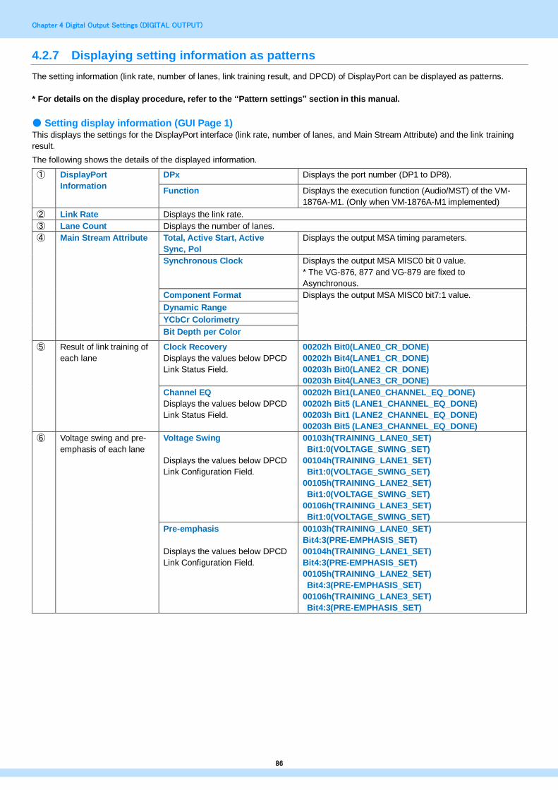
Chapter 4 Digital Output Settings (DIGITAL OUTPUT)
86
4.2.7 Displaying setting information as patterns
The setting information (link rate, number of lanes, link training result, and DPCD) of DisplayPort can be displayed as patterns.
* For details on the display procedure, refer to the “Pattern settings” section in this manual.
● Setting display information (GUI Page 1) This displays the settings for the DisplayPort interface (link rate, number of lanes, and Main Stream Attribute) and the link training
result.
The following shows the details of the displayed information.
① DisplayPort
Information
DPx Displays the port number (DP1 to DP8).
Function Displays the execution function (Audio/MST) of the VM-
1876A-M1. (Only when VM-1876A-M1 implemented)
② Link Rate Displays the link rate.
③ Lane Count Displays the number of lanes.
④ Main Stream Attribute
Total, Active Start, Active
Sync, Pol
Displays the output MSA timing parameters.
Synchronous Clock Displays the output MSA MISC0 bit 0 value.
* The VG-876, 877 and VG-879 are fixed to
Asynchronous.
Component Format Displays the output MSA MISC0 bit7:1 value.
Dynamic Range
YCbCr Colorimetry
Bit Depth per Color
⑤ Result of link training of
each lane
Clock Recovery
Displays the values below DPCD
Link Status Field.
00202h Bit0(LANE0_CR_DONE)
00202h Bit4(LANE1_CR_DONE)
00203h Bit0(LANE2_CR_DONE)
00203h Bit4(LANE3_CR_DONE)
Channel EQ
Displays the values below DPCD
Link Status Field.
00202h Bit1(LANE0_CHANNEL_EQ_DONE)
00202h Bit5 (LANE1_CHANNEL_EQ_DONE)
00203h Bit1 (LANE2_CHANNEL_EQ_DONE)
00203h Bit5 (LANE3_CHANNEL_EQ_DONE)
⑥ Voltage swing and pre-
emphasis of each lane
Voltage Swing
Displays the values below DPCD
Link Configuration Field.
00103h(TRAINING_LANE0_SET)
Bit1:0(VOLTAGE_SWING_SET)
00104h(TRAINING_LANE1_SET)
Bit1:0(VOLTAGE_SWING_SET)
00105h(TRAINING_LANE2_SET)
Bit1:0(VOLTAGE_SWING_SET)
00106h(TRAINING_LANE3_SET)
Bit1:0(VOLTAGE_SWING_SET)
Pre-emphasis
Displays the values below DPCD
Link Configuration Field.
00103h(TRAINING_LANE0_SET)
Bit4:3(PRE-EMPHASIS_SET)
00104h(TRAINING_LANE1_SET)
Bit4:3(PRE-EMPHASIS_SET)
00105h(TRAINING_LANE2_SET)
Bit4:3(PRE-EMPHASIS_SET)
00106h(TRAINING_LANE3_SET)
Bit4:3(PRE-EMPHASIS_SET)

Chapter 4 Digital Output Settings (DIGITAL OUTPUT)
87
Display example
DisplayPort Information (DP1) : VM-1876A-M1(Audio)
Link Rate : 5.4Gbps (HBR2)Lane Count : 4 lanes
---- Main Stream Attribute ----
M (at a certain time) : 18023
N : 32768
Total 2200 1125
Active Start 192 41
Active 1920 1080
Sync 44 5
Pol POSI POSI
H(dot) V(Line)
Synchronous Clock AsynchronousComponent Format RGB Dynamic Range VESA Range (Full Range)YCbCr Colorimetry ITU601Bit Depth per Color/Component 8 bits
LANE0 LANE1 LANE2 LANE3 Clock Recovery PASS PASS PASS PASS
Channel EQ PASS PASS PASS PASS
Voltage Swing 0.4V 0.4V 0.4V 0.4VPre-emphasis 0dB 0dB 0dB 0dB
①
②③
④
⑤
⑥

Chapter 4 Digital Output Settings (DIGITAL OUTPUT)
88
● DPCD display (from GUI Page 2, HEX is DPCD display only)
This displays the DisplayPort configuration data (DPCD). Change the addresses to display by changing the page.
The following shows the details of the information that can be displayed.
① Fields of Port and DPCD displaying the setting states
② DPCD addresses
③ Each parameter setting value
④ HEX display
DPCD display example (GUI)
DPCD display example (HEX)
The following items can also be displayed as patterns.
For details, refer to “Pattern Settings” in this manual.
● EDID ● DDC/CI
= = = D P CD : R e c e i v e r C a pa b i l i t y F i e l d [ P o r t = D P 1 ]
00000 D P CD _R E V : 1 1 hD P CD _R E V = 1 . 1
00001 M A X _L I N K _R A TE : 0 A h
M A X _L I N K _R A TE = 2 . 7 Gbps00002 M A X _L A N E _CO U N T : 8 4 h
M A X _L A N E _CO U N T = 4 , E N H A N CE D _F R A M E _CA P = 1
00003 M A X _D O W N S P R E A D : 0 0 hM A X _D O W N S P R E A D = 0 , N O _A U X _H A N D S H A K E _L I N K _TR A I N I N G = 0
00004 N O R P : 0 0 h
NORP = 000005 D W N _S TR E A M _P O R T_P R E S E N T : 0 0 h
D W N _S TR E A M _P O R T_P R E S E N T = 0 , D W N _S TR E A M _P O R T_TYP E = D i s p l a y P o r t
F O R M A T_CO N V E R S I O N = 000006 M A I N _ L I N K _CH A N N E L _CO D I N G : 0 0 h
M A I N _ L I N K _CH A N N E L _CO D I N G = - - -
00007 D W N _S TR E A M _P O R T_CO U N T : 0 0 hD W N _S TR E A M _P O R T_CO U N T = 0 , O U I S u ppo r t = n o t s u ppo r t e d
00008 R E CE I V E _P O R T0 _CA P 0 : 0 0 h
L O CA L _E D I D _P R E S E N T = 0 , A S S O C I A TE D _TO _P R E CE N D I N G_P O R T = 000009 R E CE I V E _P O R T0 _CA P 1 : 0 0 h
B U F F E R _S I Z E = 3 2 by t e / l a n e0000A R E CE I V E _P O R T1 _CA P 0 : 0 0 h
L O CA L _E D I D _P R E S E N T = 0 , A S S O C I A TE D _TO _P R E CE N D I N G_P O R T = 0
0000B R E CE I V E _P O R T1 _CA P 1 : 0 0 hB U F F E R _S I Z E = 3 2 by t e / l a n e
①
② ③
= = = D P CD : R e c e i v e r C a pa b i l i t y F i e l d [ P o r t = D P 1 ]
00 01 02 03 04 05 06 07 08 09 0A 0B 0C 0D 0E 0F
11 0A 84 00 00 00 00 00 00 00 00 00 00 00 00 000000 00 00 00 00 00 00 00 00 00 00 00 00 00 00 001000 00 00 00 00 00 00 00 00 00 00 00 00 00 00 002000 00 00 00 00 00 00 00 00 00 00 00 00 00 00 003000 00 00 00 00 00 00 00 00 00 00 00 00 00 00 004000 00 00 00 00 00 00 00 00 00 00 00 00 00 00 005000 00 00 00 00 00 00 00 00 00 00 00 00 00 00 006000 00 00 00 00 00 00 00 00 00 00 00 00 00 00 007000 00 00 00 00 00 00 00 00 00 00 00 00 00 00 008000 00 00 00 00 00 00 00 00 00 00 00 00 00 00 009000 00 00 00 00 00 00 00 00 00 00 00 00 00 00 00A000 00 00 00 00 00 00 00 00 00 00 00 00 00 00 00B000 00 00 00 00 00 00 00 00 00 00 00 00 00 00 00C000 00 00 00 00 00 00 00 00 00 00 00 00 00 00 00D000 00 00 00 00 00 00 00 00 00 00 00 00 00 00 00E000 00 00 00 00 00 00 00 00 00 00 00 00 00 00 00F0
①
④

Chapter 4 Digital Output Settings (DIGITAL OUTPUT)
89
4.2.8 Relationship between Pattern Rendering Bit Length and Dot Clock
The dot clock is limited by the pattern rendering bit length (color depth) and dot clock operation mode (DotClk Mode) as shown below. Furthermore, when the output bit length (video width) of the DisplayPort interface is smaller than the pattern rendering bit length (color depth), data thinning occurs. For details on the dot clock operation mode (DotClk Mode) and pattern bit length (color depth), refer to “2.1 ALL OUTPUT”.
For details on the video width, refer to “エラー! 参照元が見つかりません。 エラー! 参照元が見つかりません。”.
● DisplayPort Unit VM-1876-M1
1) When the video width is 6 bits
Data is truncated.
Data is truncated.

Chapter 4 Digital Output Settings (DIGITAL OUTPUT)
90
2) When the video width is 8 bits
3) When the video width is 10 bits
Data is truncated.
Data is truncated.
Data is truncated.
When color depth < video width (= 10 bit), "0"
data is added at the lower level.
When color depth < video width (= 10 bit), "0"
data is added at the lower level.
Data is truncated.
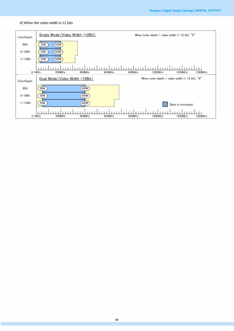
Chapter 4 Digital Output Settings (DIGITAL OUTPUT)
91
4) When the video width is 12 bits
Data is truncated.
When color depth < video width (= 12 bit), "0"
data is added at the lower level.
When color depth < video width (= 12 bit), "0"
data is added at the lower level.

Chapter 4 Digital Output Settings (DIGITAL OUTPUT)
92
● DisplayPort Unit VM-1876A-M1
* The amount of data that can be transferred (pixel clock upper limit) differs depending on the combination of the link rate and lane count. For details, refer to “4.2.1 DisplayPort Unit VM-1876A-M1”.
1) When the video width is 6 bits
The above displays the dot clock upper limit values when one image is output with two connectors (split rendering). The dot clock upper limit values when one image is output with one connector are 8 bit: 600 MHz, 9/10 bit: 576 MHz, and 11/12 bit: 480 MHz.
11/12Bit
9/10Bit
8Bit
ColorDepth
1360MHz
シングルクロックモード
25M
25M
400MHz0.1MHz 800MHz 1200MHz1000MHz600MHz200MHz
25M
データが切り捨てられます
340M
320M
340M
50M
50M11/12Bit
9/10Bit
8Bit
ColorDepth
400MHz0.1MHz 800MHz 1200MHz 1360MHz1000MHz600MHz200MHz
50M
データが切り捨てられます
デュアルクロックモード
640M
680M
680M
100M
100M11/12Bit
9/10Bit
8Bit
ColorDepth
400MHz0.1MHz 800MHz 1200MHz 1360MHz1000MHz600MHz200MHz
100M
クアッドクロックモード
1200M
1200M
1200M
データが切り捨てられます
Data is truncated.
Data is truncated.
Data is truncated.
Single clock mode
Dual clock mode
Quad clock mode

Chapter 4 Digital Output Settings (DIGITAL OUTPUT)
93
2) When the video width is 8 bits
The above displays the dot clock upper limit values when one image is output with two connectors (split rendering). The dot clock upper limit values when one image is output with one connector are 8 bit: 600 MHz, 9/10 bit: 576 MHz, and 11/12 bit: 480 MHz.
25M11/12Bit
9/10Bit
8Bit
ColorDepth
400MHz0.1MHz 800MHz 1200MHz 1360MHz1000MHz600MHz200MHz
25M
25M
データが切り捨てられます
シングルクロックモード
320M
340M
340M
50M
50M11/12Bit
9/10Bit
8Bit
ColorDepth
400MHz0.1MHz 800MHz 1200MHz 1360MHz1000MHz600MHz200MHz
データが切り捨てられます
680M50M
デュアルクロックモード
640M
680M
1200M
100M
100M11/12Bit
9/10Bit
8Bit
ColorDepth
400MHz0.1MHz 800MHz 1200MHz 1360MHz1000MHz600MHz200MHz
データが切り捨てられます
1200M
クアッドクロックモード
1200M100M
Data is truncated.
Data is truncated.
Data is truncated.
Single clock mode
Dual clock mode
Quad clock mode

Chapter 4 Digital Output Settings (DIGITAL OUTPUT)
94
3) When the video width is 10 bits
The above displays the dot clock upper limit values when one image is output with two connectors (split rendering).
The dot clock upper limit values when one image is output with one connector are 8 bit: 600 MHz, 9/10 bit: 576 MHz, and
11/12 bit: 480 MHz.
0.1MHz
25M
25M
ColorDepth
400MHz 800MHz 1200MHz 1360MHz1000MHz600MHz200MHz
11/12Bit
9/10Bit
8Bit
25M
Color Depth < Video Width (=10Bit)の場合、下位にはデータ"0"が付加されています。
データが切り捨てられます
シングルクロックモード
320M
340M
340M
400MHz0.1MHz 800MHz 1200MHz 1360MHz1000MHz600MHz200MHz
50M 680M
680M50M
50M11/12Bit
9/10Bit
8Bit
ColorDepth
Color Depth < Video Width (=10Bit)の場合、下位にはデータ"0"が付加されています。
データが切り捨てられます640M
デュアルクロックモード
400MHz0.1MHz 800MHz 1200MHz 1360MHz1000MHz600MHz200MHz
100M
100M
100M11/12Bit
9/10Bit
8Bit
ColorDepth
Color Depth < Video Width (=10Bit)の場合、下位にはデータ"0"が付加されています。
データが切り捨てられます
1200M
1200M
1200M
クアッドクロックモード
Single clock mode
Dual clock mode
Quad clock mode
Data is truncated.
Data is truncated.
Data is truncated.
When color depth < video width (= 10 bit), "0"
data is added at the lower level.
When color depth < video width (= 10 bit), "0"
data is added at the lower level.
When color depth < video width (= 10 bit), "0"
data is added at the lower level.

Chapter 4 Digital Output Settings (DIGITAL OUTPUT)
95
4) When the video width is 12 bits
The above displays the dot clock upper limit values when one image is output with two connectors (split rendering). The dot clock upper limit values when one image is output with one connector are 8 bit: 600 MHz, 9/10 bit: 576 MHz, and 11/12 bit: 480 MHz.
25M 340M
340M
320M
25M
25M11/12Bit
9/10Bit
8Bit
ColorDepth
0.1MHz 400MHz 800MHz 1200MHz 1360MHz1000MHz600MHz200MHz
Color Depth < Video Width (=12Bit)の場合、下位にはデータ"0"が付加されています。
シングルクロックモード
データが切り捨てられます
680M
680M
640M
50M
50M
50M11/12Bit
9/10Bit
8Bit
ColorDepth
400MHz0.1MHz 800MHz 1200MHz 1360MHz1000MHz600MHz200MHz
データが切り捨てられます
Color Depth < Video Width (=12Bit)の場合、下位にはデータ"0"が付加されています。
デュアルクロックモード
100M
100M
100M11/12Bit
9/10Bit
8Bit
ColorDepth
400MHz0.1MHz 800MHz 1200MHz 1360MHz1000MHz600MHz200MHz
データが切り捨てられます
Color Depth < Video Width (=12Bit)の場合、下位にはデータ"0"が付加されています。
1200M
1200M
1200M
クアッドクロックモード
Single clock mode
Dual clock mode
Quad clock mode
Data is truncated.
Data is truncated.
Data is truncated.
When color depth < video width (= 12 bit), "0"
data is added at the lower level.
When color depth < video width (= 12 bit), "0"
data is added at the lower level.
When color depth < video width (= 12 bit), "0"
data is added at the lower level.

Chapter 4 Digital Output Settings (DIGITAL OUTPUT)
96
4.3 SDI unit functions and settings
The applicable unit is as follows.
4.3.1 SDI Unit VM-1876-M5
● Unit exterior diagram
No. Name Description
① SDI output Outputs in the specified format from four BNC connectors.
② Standby LED Lights when output preparation is complete. On: Normal
Off: Error (module damaged, wrong slot, etc.)
4.3.2 12G-SDI Unit VM-1876-MB
● Unit exterior diagram
No. Name Description
① SDI output Outputs in the specified format from four BNC connectors.
② Standby LED Lights when output preparation is complete. On: Normal
Off: Error (module damaged, wrong slot, etc.)
③ External synchronization
output
Outputs an external synchronization signal (3CS/BB). * Support in the future.
① ②
① ② ③

Chapter 4 Digital Output Settings (DIGITAL OUTPUT)
97
● Specifications
SDI output is only at the timing corresponding to each supported SDI standard (SMPTE) below.
[Component image format SMPTE 259M]
Rate Standard Details
270 Mb/s
SMPTE 259M
SD-SDI
Interlace
720 x 480,
720 x 525
525/59.94i
625/50i YCbCr 4:2:2 10 bit
[1080 Line source image format SMPTE 274M]
Rate Standard Details
1.485 Gb/s
SMPTE 274M
HD-SDI
Interlace
Progressive
Segmented Frame
1920 x 1080
60i, 59.94i,
30p, 29.97p,
50i, 25p,
24p, 23.98p,
30PsF, 29.97PsF,
25PsF, 24PsF,
23.98PsF
YCbCr 4:2:2 10 bit
[720 Line source image format SMPTE 296M]
Rate Standard Details
1.485 Gb/s
SMPTE296M
HD-SDI
Progressive
1280 x 720
60p, 59.94p,
50p, 25p,
30p, 29.97p,
24p, 23.98p
YCbCr 4:2:2 10 bit
[1080 Line source image format SMPTE 372]
Rate Standard Details
1.485 Gb/s
x2
SMPTE 372M
DUAL LINK
Progressive
1920 x 1080 60p, 59.94p, 50p YCbCr 4:2:2 10 bit
SMPTE 372M
DUAL LINK
Interlace
Progressive
Segmented Frame
1920 x 1080
60i, 59.94i,
30p, 29.97p,
25p, 24p, 23.98p,
30PsF, 29.97PsF,
25PsF, 24PsF,
23.98PsF
YCbCr 4:2:2 12 bit
YCbCr 4:4:4 10 bit
YCbCr 4:4:4 12 bit
RGB 4:4:4 10 bit
RGB 4:4:4 12 bit
SMPTE 372M
DUAL LINK
Progressive
Segmented Frame
2048 x 1080
60i, 59.94i,
30p, 29.97p,
25p, 24p, 23.98p,
30PsF, 29.97PsF,
25PsF, 24PsF,
23.98PsF
YCbCr 4:2:2 12 bit
YCbCr 4:4:4 10 bit
YCbCr 4:4:4 12 bit
RGB 4:4:4 10 bit
RGB 4:4:4 12 bit

Chapter 4 Digital Output Settings (DIGITAL OUTPUT)
98
[1080/720 Line source image format SMPTE 425-1]
Rate Standard Details
2.97 Gb/s
SMPTE ST 425-1
3G-SDI
Progressive
1920 x 1080 60p, 59.94p, 50p YCbCr 4:2:2 10 bit
SMPTE ST 425-1
3G-SDI
Progressive
2048 x 1080 60p, 59.94p, 50p,
48p, 47.95p YCbCr 4:2:2 10 bit
SMPTE ST 425-1
3G-SDI
Interlace
Progressive
Segmented Frame
1920 x 1080
60i, 59.94i, 50i,
30p, 29.97p, 25p,
24p, 23.98p
30PsF, 29.97PsF,
25PsF,
24PsF, 23.98PsF
YCbCr 4:2:2 12 bit
YCbCr 4:4:4 10 bit
YCbCr 4:4:4 12 bit
RGB 4:4:4 10 bit
RGB 4:4:4 12 bit
SMPTE ST 425-1
3G-SDI
Progressive
1280 x 720
60p, 59.94p, 50p,
30p, 29.97p, 25p,
24p, 23.98p
YCbCr 4:4:4 10 bit
RGB 4:4:4 10 bit
* 4:4:4 format of 720p supports only Level.A.
[2160/1080 Line source image format SMPTE 425-3]
Rate Standard Details
2.97 Gb/s
x2
SMPTE ST 425-3
3G-SDI Dual Link
Progressive
1920 x 1080 60p, 59.94p, 50p
YCbCr 4:2:2 12 bit
YCbCr 4:4:4 10 bit
RGB 4:4:4 10 bit
SMPTE ST 425-3
3G-SDI Dual Link
Progressive
2048 x 1080 60p, 59.94p, 50p,
48p, 47.95p
YCbCr 4:2:2 12 bit
YCbCr 4:4:4 10 bit
RGB 4:4:4 10 bit
SMPTE ST 425-3
3G-SDI Dual Link
Progressive : 2SI
3840 x 2160 30p, 29.97p, 25p,
24p, 23.98p
YCbCr 4:2:2 10 bit
YCbCr 4:2:0 10 bit
SMPTE ST 425-3
3G-SDI Dual Link
Progressive : 2SI
4096 x 2160 30p, 29.97p, 25p,
24p, 23.98p YCbCr 4:2:2 10 bit
* 2160 Line supports only Level.B.

Chapter 4 Digital Output Settings (DIGITAL OUTPUT)
99
[2160 Line source image format SMPTE 425-5]
Rate Standard Details
2.97 Gb/s
x4
SMPTE ST 425-1
3G-SDI Quad Link
Progressive
3840 x 2160 60p, 59.94p, 50p YCbCr 4:2:2 10 bit
YCbCr 4:2:0 10 bit
SMPTE ST 425-1
3G-SDI Quad Link
Progressive
4096 x 2160 60p, 59.94p, 50p,
48p, 47.95p YCbCr 4:2:2 10 bit
SMPTE ST 425-1
3G-SDI Quad Link
Progressive
3840 x 2160 30p, 29.97p, 25p,
24p, 23.98p
YCbCr 4:2:2 12 bit
YCbCr 4:4:4 10 bit
YCbCr 4:4:4 12 bit
RGB 4:4:4 10 bit
RGB 4:4:4 12 bit
SMPTE ST 425-1
3G-SDI Quad Link
Progressive
4096 x 2160 30p, 29.97p, 25p,
24p, 23.98p
YCbCr 4:2:2 12 bit
YCbCr 4:4:4 10 bit
YCbCr 4:4:4 12 bit
RGB 4:4:4 10 bit
RGB 4:4:4 12 bit
[2160Line source image format HD-SDI Quad Link]
Rate Standard Details
1.485 Gb/s
x4
Quad LINK
Progressive
Segmented Frame
3840 x 2160
30p, 29.97p, 25p,
24p, 23.98p
30PsF, 29.97PsF,
25PsF,
24PsF, 23.98PsF
YCbCr 4:2:2 10 bit
Quad LINK
Progressive
Segmented Frame
4096 x 2160
30p, 29.97p, 25p,
24p, 23.98p
30PsF, 29.97PsF,
25PsF,
24PsF, 23.98PsF
YCbCr 4:2:2 10 bit

Chapter 4 Digital Output Settings (DIGITAL OUTPUT)
100
[2160/1080 Line source image format SMPTE 2081-10] * Only supported for VM-1876-MB.
Rate Standard Details
5.94 Gb/s
SMPTE ST 2081-10
6G-SDI
Progressive : 2SI
1920 x 1080 60p, 59.94p, 50p
YCbCr 4:2:2 12 bit
YCbCr 4:4:4 10 bit
YCbCr 4:4:4 12 bit
RGB 4:4:4 10 bit
RGB 4:4:4 12 bit
SMPTE ST 2081-10
6G-SDI
Progressive : 2SI
2048 x 1080 60p, 59.94p, 50p,
48p, 47.95p
YCbCr 4:2:2 12 bit
YCbCr 4:4:4 10 bit
YCbCr 4:4:4 12 bit
RGB 4:4:4 10 bit
RGB 4:4:4 12 bit
SMPTE ST 2081-10
6G-SDI
Progressive : 2SI
3840 x 2160 30p, 29.97p, 25p,
24p, 23.98p
YCbCr 4:2:2 10 bit
YCbCr 4:2:0 10 bit
SMPTE ST 2081-10
6G-SDI
Progressive : 2SI
4096 x 2160 30p, 29.97p, 25p,
24p, 23.98p YCbCr 4:2:2 10 bit
[2160 Line source image format SMPTE 2081-11] * Only supported for VM-1876-MB.
Rate Standard Details
5.94 Gb/s
x2
SMPTE ST 2081-10
6G-SDI Dual Link
Progressive : 2SI
3840 x 2160 60p, 59.94p, 50p YCbCr 4:2:2 10 bit
YCbCr 4:2:0 10 bit
SMPTE ST 2081-10
6G-SDI Dual Link
Progressive : 2SI
4096 x 2160 60p, 59.94p, 50p,
48p, 47.95p YCbCr 4:2:2 10 bit
SMPTE ST 2081-10
6G-SDI Dual Link
Progressive : 2SI
3840 x 2160 30p, 29.97p, 25p,
24p, 23.98p
YCbCr 4:2:2 12 bit
YCbCr 4:2:0 12 bit
YCbCr 4:4:4 10 bit
YCbCr 4:4:4 12 bit
RGB 4:4:4 10 bit
RGB 4:4:4 12 bit
SMPTE ST 2081-10
6G-SDI Dual Link
Progressive : 2SI
4096 x 2160 30p, 29.97p, 25p,
24p, 23.98p
YCbCr 4:2:2 12 bit
YCbCr 4:4:4 10 bit
YCbCr 4:4:4 12 bit
RGB 4:4:4 10 bit
RGB 4:4:4 12 bit

Chapter 4 Digital Output Settings (DIGITAL OUTPUT)
101
[2160 Line source image format SMPTE 2082-10] * Only supported for VM-1876-MB.
Rate Standard Details
11.88 Gb/s
SMPTE2082-10
12G-SDI
Progressive : 2SI
3840 x 2160 60p, 59.94p, 50p YCbCr 4:2:2 10 bit
YCbCr 4:2:0 10 bit
SMPTE2082-10
12G-SDI
Progressive : 2SI
4096 x 2160 60p, 59.94p, 50p,
48p, 47.95p
YCbCr 4:2:2 10 bit
YCbCr 4:2:0 10 bit
SMPTE2082-10
12G-SDI
Progressive : 2SI
3840 x 2160 30p, 29.97p, 25p,
24p, 23.98p
YCbCr 4:2:2 12 bit
YCbCr 4:2:0 12 bit
YCbCr 4:4:4 10 bit
YCbCr 4:4:4 12 bit
RGB 4:4:4 10 bit
RGB 4:4:4 12 bit
SMPTE2082-10
12G-SDI
Progressive : 2SI
4096 x 2160 30p, 29.97p, 25p,
24p, 23.98p
YCbCr 4:2:2 12 bit
YCbCr 4:4:4 10 bit
YCbCr 4:4:4 12 bit
RGB 4:4:4 10 bit
RGB 4:4:4 12 bit

Chapter 4 Digital Output Settings (DIGITAL OUTPUT)
102
4.3.3 SDI data transfer method
● SD-SDI and HD-SDI signals The signals are output from the BNC connectors without being
split.
● SMPTE372M (DUAL LINK) Assigns to outputs 1 and 2 (3 and 4) is performed from the
lowest slot number to output as follows.
BNC terminal Signal name
CH1 Output 1 (3) LINK A
CH2 Output 1 (3) LINK B
CH3 Output 2 (4) LINK A
CH4 Output 2 (4) LINK B
● 3G-SDI signal The signals are output from the BNC connectors without being
split.
● 4K 3840x2160 (4096x2160) signals [VM-1876-M5]
The signals are mapped to 3G-SDI or mapped to SMPTE372M
(DUAL LINK) and then output.
[VM-1876-MB]
The signals are mapped in accordance with various standards
to 3G-SDI/6G-SDI/12G-SDI or mapped to HD-SDI and then
output.
The mapping method is as follows.
Mode 0 4Square Division (4 quarter panes)
The 3840x2160 format which cannot be represented with the
resolution of an HD-SDI signal is split into 4 quarter panes and
then output.
Mode A 2-sample interleave division (2SI)
The 3840x2160 format which cannot be represented with
the resolution of an HD-SDI signal is split as follows and then output.
3
100
4
2101 2 104 2105 2
3 4 3 43 4
3
120
4
2121 2 124 2125 2
3 4 3 43 4
100 101 104 105
120 121 124 125
Example: When channel 1 output Images containing a collection of groups (pixels classified by color) consisting of 2 pixels and 2 lines are output. Output channels 1 to 4 output the data as images containing a
collection of ① to ④.
The signals that were split in this way are mapped to 3G-SDI and then output.
Lane 1-4 Lane 9-12
Lane 5-8 Lane 13-16

Chapter 4 Digital Output Settings (DIGITAL OUTPUT)
103
4.3.4 SDI output setting items
Level 1 Level 2 Level 3 Setting item Setting value
SDI
Output
OFF/ON
Port1 to Port16
Sets ON/OFF for each Port.
0: OFF / 1: ON
* The following cannot be set when other than Refer Program is selected for Mode in the SDI payload settings.
SDI Format
Sets the SDI format.
0: SD
1: HD
2: 3G-A
3: 3G-B
4: Dual HD
5: 6G * VM-1876-MB only
6: 12G * VM-1876-MB only
Video Format
Sets the color space of video output from SDI.
0: RGB
1: YCbCr4:4:4
2: YCbCr4:2:2:
3: YCbCr4:2:0 * VM-1876-MB
only
Width
Sets the output video bit length. This can be set to a bit length that is
independent of pattern rendering, or the same bit length can be selected
automatically.
* The portion of the bit length of pattern rendering that exceeds the bit
length set here will be truncated. Furthermore, if there is a missing portion, it
will be compensated for with “0.”
0: Auto
1: 10 bit
2: 12 bit
Split Count
Sets the number of screen splits.
* This is in accordance with the DotClk Mode setting in “2.1 ALL OUTPUT”.
0: No Split
1: 2Split(not use)
2: 4Split
Split Mode
Sets the split mode.
* This is in accordance with the Split Mode setting of the DotClk Mode
setting in “2.1 ALL OUTPUT”.
* Displayed only when 4Split
0: 4square
1: reserved1
2: reserved1
3. reserved1
4: reserved1
5: reserved1
6: reserved1
6: reserved1
7: reserved1
8: reserved1
9: reserved1
A: 2SI
Audio Output
Sets embedded audio output.
0: OFF / 1: ON
Audio Copy Ch2
Audio Copy Ch3
Audio Copy Ch4
Sets whether or not to copy the audio of the channel 2 and subsequent
channels of 3G SDI from Link 1.
0: No Copy
Superimposes the audio data
of only Link 1 (channel 1).
1: Copy Ch1
Copies the same audio data
as Link 1 (channel 1) to
channels 2, 3, and 4.

Chapter 4 Digital Output Settings (DIGITAL OUTPUT)
104
4.3.5 Payload
* These settings are only for payload identification data. For the settings that directly affect transmission signals, refer to each
corresponding item.
* When the VM-1876-M5 is used, the payload settings cannot be configured when SD output is set.
Level 1 Level 2 Level 3 Setting item Setting value
Payload
OFF/ON
Enables payload identification data.
[VM-1876-M5]
0: OFF
Does not multiplex the Payload ID.
1: ON
Multiplexes the Payload ID.
[VM-1876-MB]
0: OFF
Does not multiplex the Payload ID.
1: Y ON
Multiplexes the Payload ID with the Y
stream.
2: C ON
Multiplexes the Payload ID with the C
stream.
3: Y/C ON
Multiplexes the Payload ID with the Y/C
stream.
When OFF, the Mode and subsequent settings are not displayed.
Mode
Determines the payload setting method.
0: Refer Program
Determines the payload setting values
depending on the SDI output data
settings.
* Byte 1 and lower are not displayed.
1: Manual
Sets the payload settings manually.
* Settings other than payload settings
are not reflected.
* SDI output settings become no longer
able to be configured.
2: Hex
Sets byte 1 to byte 4 of the payload with
hex settings
* SDI output settings become no longer
able to be configured.
Byte1
Sets the byte.
00h to FFh
The following are displayed when Mode = 1: Manual is set.
Transport
Sets the transport scan mode.
0: Interlace
1: Progressive
Picture
Sets the picture scan mode.
0: Interlace
1: Progressive
Picture Rate
Sets the frame rate.
0: 23.98 Hz
1: 24 Hz
2: 25 Hz
3: 29.97 Hz
4: 30 Hz
5: 50 Hz
6: 59.94 Hz
7: 60 Hz
8: 47.95 Hz
9: 48 Hz
Aspect Ratio
Sets the aspect ratio.
*The bits that can be set vary depending on the setting of byte 1.
0: 4:3
Aspect ratio 4:3
1: 16:9
Aspect ratio 16:9

Chapter 4 Digital Output Settings (DIGITAL OUTPUT)
105
Level 1 Level 2 Level 3 Setting item Setting value
H Y-Sampling
Sets the H or Y sampling value.
0: 2
1: 1
Sampling Struc
Sets the sampling structure (video format).
0: 4:2:2(YCbCr)
1: 4:4:4(YCbCr)
2: 4:4:4(RGB)
3: 4:4:4:4(YCbCr+A)
4: 4:4:4:4(RGB+A)
5: 4:4:4(XYZ)
6: 4:2:0
7: 4:2:2:4(YCbCr+A)
8: 4:2:2:4(YCbCr+D)
9: 4:4:4:4(YCbCr+D)
A: 4:4:4:4(RGB+D)
Ch1 LinkA
Ch1 LinkB
Ch2 LinkA
Ch2 LinkB
Ch3 LinkA
Ch3 LinkB
Ch4 LinkA
Ch4 LinkB
Sets the data stream.
0: Stream1(0h)
1: Stream2(2h)
2: Stream3(4h)
3: Stream4(6h)
4: Stream5(8h)
5: Stream6(Ah)
6: Stream7(Ch)
7: Stream8(Eh)
Audio Copy Ch1
Audio Copy Ch2
Audio Copy Ch3
Audio Copy Ch4
Sets whether or not to copy the audio of the Link 2 and
subsequent channels of 3G SDI from Link 1.
0: No Copy
Superimposes the audio data of only
Link 1 (channel 1).
1: Copy Link1
Copies the same audio data as Link 1
(channel 1) to channels 2, 3, and 4.
Dynamic Range
Set the dynamic range.
0: 100%
1: 200%
2: 400%
Bit Depth
Sets the bit length.
0: 8bit
1: 10 bit
2: 12 bit
Transfer
SetstheTransfer characteristics.
0:SDR-TV
1:HLG
2:PQ
3:Unspecified
Colorimetry
Sets the Colorimetry.
0:Rec709
1:Reserved
2:UHDTV
3:Unknown
Luminance
Sets the Luminance and color difference signal.
0:Y’C’bC’r
1:ICtCp
The following are displayed when Mode = 2: Hex is set.
Byte 2
Sets byte 2.
00h to FFh
Byte 3
Sets byte 3.
00h to FFh
Byte 4 Ch1 LinkA
Sets byte 4 of Channel 1 Link A.
00h to FFh
Byte 4 Ch1 LinkB
Sets byte 4 of Channel 1 Link B.
00h to FFh
Byte 4 Ch2 LinkA
Sets byte 4 of Channel 2 Link A.
00h to FFh
Byte 4 Ch2 LinkB
Sets byte 4 of Channel 2 Link B.
00h to FFh
Byte 4 Ch3 LinkA
Sets byte 4 of Channel 3 Link A.
00h to FFh
Byte 4 Ch3 LinkB 00h to FFh

Chapter 4 Digital Output Settings (DIGITAL OUTPUT)
106
Level 1 Level 2 Level 3 Setting item Setting value
Sets byte 4 of Channel 3 Link B.
Byte 4 Ch4 LinkA
Sets byte 4 of Channel 4 Link A.
00h to FFh
Byte 4 Ch4 LinkB
Sets byte 4 of Channel 4 Link B.
00h to FFh

Chapter 4 Digital Output Settings (DIGITAL OUTPUT)
107
4.3.6 SDI configuration setting items
This section describes configuration settings for the SDI unit.
Set these settings from MENU > Configuration.
[VM-1876-M5]
Level 1 Level 2 Level 3 Setting item Setting value
Configuration
SDI Configuration SDI Setting Time Code
Time Code OFF/ON 0: OFF
Does not insert a time code.
1: ON
Inserts a time code.
Start Time Set h(0 - 23) :m(0 - 59) : s(0 - 59)
Sets the time of Time Code.
Time Set Sets the time set in Start Time.
Configuration SDI Setting Clock Delay
Delay Clock1 - 8
Sets the delay on a clock
basis for the SDI signal.
This cannot be set when
SDI output.
Sign: Sign (delay/advance)
0: +
Advances by the clock amount set in Time.
1: -
Delays by the clock amount set in Time.
Time: Sets the time. (Value that is half of the 0 to H period)
[VM-1876-MB]
Level 1 Level 2 Level 3 Setting item Setting value
Configuration
SDI Configuration SDI Setting Time Code
VITC Time Code OFF/ON 0: OFF
Does not insert VITC.
1: ON
Inserts VITC.
LTC Time Code OFF/ON 0: OFF
Does not insert LTC.
1: ON
Inserts LTC.
Drop Frame OFF/ON 0: OFF
Does not use drop frames.
1: ON
Uses drop frames.
* Applicable only when 29.97, 59.94 fps.
Start Time h(0 - 23) :m(0 - 59) : s(0 - 59)
Sets the time of Time Code.
Time Set Sets the time set in Start Time.
Hold Pauses the time code.
Reset Resets the counter to zero for the time code.
Configuration SDI Setting Clock Delay
Delay Clock1 - 8
Sets the delay on a clock
basis for the SDI signal.
This cannot be set when SDI
output.
Sign: Sign (delay/advance)
0: +
Advances by the clock amount set in Time.
1: -
Delays by the clock amount set in Time.
Time: Sets the time. (Value that is half of the 0 to H period)

Chapter 4 Digital Output Settings (DIGITAL OUTPUT)
108
[VM-1876-MB]
Level 1 Level 2 Level 3 Setting item Setting value
Configuration
SDI Configuration SDI Setting Other
Ancillary Packet
Multiplexes arbitrary
ancillary data specified by
the user with SDI signals.
ANC Packet OFF/ON 0: OFF
Does not insert the ANC
packet.
1: Y ON
Inserts the ANC packet in the Y
stream.
2: C ON
Inserts the ANC packet in the C
stream.
Embed Line1
Specifies the line for multiplexing
the ANC packet.
When '0,' does not multiplex.
0 - VTotal
Embed Sample1
Specifies the sample position for
multiplexing the ANC packet.
When '0,' does not multiplex.
0 - HTotal
Embed Line2
Specifies the line for multiplexing
the ANC packet.
When '0,' does not multiplex.
0 - VTotal
Embed Sample2
Specifies the sample position for
multiplexing the ANC packet.
When '0,' does not multiplex.
0 - HTotal
Parity OFF/ON 0: OFF
Does not automatically
calculate the parity.
1: ON
Automatically calculates the
parity.
DID
Sets the DID data.
Set this with 8 bit/10 bit
depending on the Parity setting.
When Parity = OFF: 10 bit
0 to 0x2FF
When Parity = ON: 8 bit
0 to 0xFF
SDID
Sets the SDID data.
Set this with 8 bit/10 bit
depending on the Parity setting.
DC
Sets the DC data.
Set this with 8 bit/10 bit
depending on the Parity setting.
When '0,' does not multiplex.
UDW[ 1 - UDW 255
Sets the user data word.
Set this with 8 bit/10 bit
depending on the Parity setting.
Enables the data for the number
of DC settings. However, the
maximum is 255.
When '0,' does not multiplex.
CheckSum Calc OFF/ON 0: Manual
Uses a user checksum.
1: Auto
Automatically calculates the
checksum.

Chapter 4 Digital Output Settings (DIGITAL OUTPUT)
109
Level 1 Level 2 Level 3 Setting item Setting value
CheckSum
Sets the user specified checksum
with 10 bits.
0x00 to 0x2FF
External Synchronization
Performs external
synchronization.
0: OFF
1: BB
2: 3CS

Chapter 4 Digital Output Settings (DIGITAL OUTPUT)
110
4.4 V-by-One HS unit functions and settings
The applicable unit is as follows.
4.4.1 V-by-One HS Unit VM-1876-M2
● Unit exterior diagram
① V-by-One HS outputs The output of four lanes per connector can be performed.
② Standby LED Lights when output preparation is complete. On: Normal Off: Error (module damaged, wrong slot, etc.)
● Specifications
V-by-One HS CH1 CH2 CH3 CH4
Connector V-by-One HS×4 (16Lane)
Dot clock
Number of data lanes: 1 lane
Single clock mode
8 bit: 20 to 85 MHz
10 bit: 20 to 85 MHz
12 bit: 20 to 75 MHz
Number of data lanes: 2 lanes
Single clock mode
8 bit: 40 to 170 MHz
10 bit: 40 to 170 MHz
12 bit: 40 to 150 MHz
Number of data lanes: 4 lanes
Single clock mode
8 bit: 80 to 340 MHz
10 bit: 80 to 340 MHz
12 bit: 80 to 300 MHz
Number of data lanes: 8 lanes
Dual clock mode *1
8 bit: 160 to 680 MHz
10 bit: 160 to 680 MHz
12 bit: 160 to 600 MHz
Number of data lanes: 16 lanes
Quad clock mode *2
8 bit: 320 to 1360 MHz
10 bit: 320 to 1360 MHz
12 bit: 320 to 1200 MHz
No. of colors 8/10/12 bit for each R, G, and B (RGB/YCbCr supported)
*1 Uses CH1-CH2 (CH3-CH4) for 8-lane output. *2 Uses CH1-CH2-CH3-CH4 for 16-lane output.
① ②

Chapter 4 Digital Output Settings (DIGITAL OUTPUT)
111
4.4.2 Connector and pin assignment
● Connector: Hosiden TCX3250-111387
Pin No. Signal
1 TX Lane0(p)
2 GND
3 TX Lane0(n)
4 TX Lane1(p)
5 GND
6 TX Lane1(n)
7 TX Lane2(p)
8 GND
9 TX Lane2(n)
10 TX Lane3(p)
11 GND
12 TX Lane3(n)
13 GND
14 GND
15 SCL
16 GND
17 SDA
18 HTPDN
19 LOCKN
20 NC
(Connectors 1 to 4 are common.)

Chapter 4 Digital Output Settings (DIGITAL OUTPUT)
112
4.4.3 V-by-OneHS data transfer method
● <Normal MODE: 2-lane Output>
The case of a 1920 x 1080@60 Hz resolution, 148 MHz dot
clock, and 10-bit output gradation is explained as an example.
Data transfer method
Assignment of each lane
● <Normal MODE: 4-lane Output>
The case of a 1920 x 1080@120Hz resolution, 297 MHz dot
clock, and 10-bit output gradation is explained as an example.
Data transfer method
Assignment of each lane
RGB 8-12bit[11:0]
RGB 8-12bit[11:0]
RGB 8-12bit[11:0]
RGB 8-12bit[11:0]
1CHConnector
Lane 1
RGB 8-12bit[11:0]
RGB 8-12bit[11:0]
RGB 8-12bit[11:0]
RGB 8-12bit[11:0]
2CHConnector
Lane 2
Lane 1
Lane 2
Lane 1
Lane 2
Lane 1
Lane 2
D 0 D2 D4 D6
・・・
・・・
D1 D3 D5 D7
[9:0] [9:0] [9:0] [9:0][9:0] [9:0] [9:0] [9:0]
・・・ [9:0] [9:0] [9:0] [9:0][9:0] [9:0] [9:0] [9:0]
CLK74MHz
L0~L1079
L0~L1079
Lane 1
Lane 2
D1912 D1914 D1916 D1918
D1913 D1915 D1917 D1919
Lane 1 Lane 2
RGB 8-12bit[11:0]
RGB 8-12bit[11:0]
RGB 8-12bit[11:0]
RGB 8-12bit[11:0]
1CHConnector
Lane 1
RGB 8-12bit[11:0]
RGB 8-12bit[11:0]
RGB 8-12bit[11:0]
RGB 8-12bit[11:0]
2CHConnector
Lane 2
Lane 3
Lane 4
Lane 1
Lane 2
Lane 3
Lane 4
D 0 D 4 D 8 D 12
・・・
・・・
D 3 D 7 D 11 D 15
D 2 D 6 D 10 D 14
D 1 D 5 D 9 D 13・・・
[9:0] [9:0] [9:0] [9:0][9:0] [9:0] [9:0] [9:0]
[9:0] [9:0] [9:0] [9:0][9:0] [9:0] [9:0] [9:0]
・・・ [9:0] [9:0] [9:0] [9:0][9:0] [9:0] [9:0] [9:0]
・・・ [9:0] [9:0] [9:0] [9:0][9:0] [9:0] [9:0] [9:0]
CLK74MHz
L0~L1079
L0~L1079
L0~L1079
L0~L1079
Lane 1
Lane 2
Lane 3
Lane 4
D 1904 D 1908 D 1912 D 1916
D 1907 D 1911 D 1915 D 1919
D 1906 D 1910 D 1914 D 1918
D 1905 D 1909 D 1913 D 1917
Lane 3 Lane 4Lane 1 Lane 2

Chapter 4 Digital Output Settings (DIGITAL OUTPUT)
113
The case of a 4096 x 2160@30 Hz resolution, 297 MHz dot
clock, and 10-bit output gradation is explained as an example.
Data transfer method
Assignment of each lane
D 0 D 4 D 8 D 12
・・・
・・・
D 3 D 7 D 11 D 15
D 2 D 6 D 10 D 14
D 1 D 5 D 9 D 13・・・
[9:0] [9:0] [9:0] [9:0][9:0] [9:0] [9:0] [9:0]
[9:0] [9:0] [9:0] [9:0][9:0] [9:0] [9:0] [9:0]
・・・ [9:0] [9:0] [9:0] [9:0][9:0] [9:0] [9:0] [9:0]
・・・ [9:0] [9:0] [9:0] [9:0][9:0] [9:0] [9:0] [9:0]
CLK74MHz
L0~L2159
L0~L2159
L0~L2159
L0~L2159
Lane 1
Lane 2
Lane 3
Lane 4
D 4092
D 4095
D 4094
D 4093
D 4088
D 4091
D 4090
D 4089
D 4084
D 4087
D 4086
D 4085
D 4080
D 4083
D 4082
D 4081
Lane 3 Lane 4Lane 1 Lane 2

Chapter 4 Digital Output Settings (DIGITAL OUTPUT)
114
● <Specifications of each mode when x4 mode output>
One screen is output with a combination of 8 lanes when full HD 240 Hz mode output. This is basically the same as the transmission method of 4K-60P. From Mode 0 (x4 mode) to Mode 4 (x4 mode) is explained here.
[Full HD 240 Hz 8-lane Output]
① Mode 0 (x4 mode) (8 lanes ) - Mode0 x4 mode (Non
Dividing Mode)
Output is with the pixel assignment shown below without splitting the screen and uses lanes 1 to 8. The case of a 1920 x 1080 resolution, 594 MHz dot clock, and 10-bit output gradation is explained as an example.
Data transfer method
Assignment of each lane
RGB 8-12bit[11:0]
RGB 8-12bit[11:0]
RGB 8-12bit[11:0]
RGB 8-12bit[11:0]
1CHConnector
Lane 1
RGB 8-12bit[11:0]
RGB 8-12bit[11:0]
RGB 8-12bit[11:0]
RGB 8-12bit[11:0]
2CHConnector
Lane 2
Lane 3
Lane 4
Lane 5
Lane 6
Lane 7
Lane 8
D 0
D 4
D 8
D 12
・・・
・・・D 1904
D 1908
D 1912
D 1916
D 3
D 7
D 11
D 15
・・・D 1907
D 1911
D 1915
D 1919
D 1906
D 1910
D 1914
D 1918
・・・D 2
D 6
D 10
D 14
D 1
D 5
D 9
D 13
・・・D 1905
D 1909
D 1913
D 1917
[9:0] [9:0] [9:0] [9:0][9:0] [9:0] [9:0] [9:0]
[9:0] [9:0] [9:0] [9:0][9:0] [9:0] [9:0] [9:0]
[9:0] [9:0] [9:0] [9:0][9:0] [9:0] [9:0] [9:0]
[9:0] [9:0] [9:0] [9:0][9:0] [9:0] [9:0] [9:0]
・・・ [9:0] [9:0] [9:0] [9:0][9:0] [9:0] [9:0] [9:0]
・・・ [9:0] [9:0] [9:0] [9:0][9:0] [9:0] [9:0] [9:0]
・・・ [9:0] [9:0] [9:0] [9:0][9:0] [9:0] [9:0] [9:0]
・・・ [9:0] [9:0] [9:0] [9:0][9:0] [9:0] [9:0] [9:0]
D 16
D20
D 24
D 28
D 19
D23
D 27
D31
D 18
D22
D26
D 30
D17
D 21
D 25
D 29
D1888
D1892
D1896
D1900
D1891
D1985
D1899
D1903
D1890
D1894
D1898
D1902
D1889
D1983
D1897
D1901
CLK74MHz
L0~L1079
L0~L1079
L0~L1079
L0~L1079
L0~L1079
L0~L1079
L0~L1079
L0~L1079
Lane 1
Lane 2
Lane 3
Lane 4
Lane 5
Lane 6
Lane 7
Lane 8
Lane 1 Lane 2 Lane 3
Lane 5-6 Lane 7-8Lane 1-2 Lane 3-4
Lane4 Lane 5 Lane 6 Lane 7 Lane 8

Chapter 4 Digital Output Settings (DIGITAL OUTPUT)
115
② Mode 1 (x4 mode) ( 8 lanes ) - Normal Mode
Output is with the pixel assignment shown below without splitting the screen and uses lanes 1 to 8. The case of a 1920 x 1080 resolution, 594 MHz dot clock, and 10-bit output gradation is explained as an example.
Data transfer method
Assignment of each lane
③ Mode 2 (x4 mode) ( 8 lanes ) - Cross Mode
Output is with the pixel assignment shown below without splitting the screen and uses lanes 1 to 8. The case of a 1920 x 1080 resolution, 594 MHz dot clock, and 10-bit output gradation is explained as an example.
Data transfer method
Assignment of each lane
・・・
・・・
・・・
・・・
[9:0] [9:0] [9:0] [9:0][9:0] [9:0] [9:0] [9:0]
[9:0] [9:0] [9:0] [9:0][9:0] [9:0] [9:0] [9:0]
[9:0] [9:0] [9:0] [9:0][9:0] [9:0] [9:0] [9:0]
・・・ [9:0] [9:0] [9:0] [9:0][9:0] [9:0] [9:0] [9:0]
・・・ [9:0] [9:0] [9:0] [9:0][9:0] [9:0] [9:0] [9:0]
・・・ [9:0] [9:0] [9:0] [9:0][9:0] [9:0] [9:0] [9:0]
CLK74MHz
L0~L1079
L0~L1079
L0~L1079
L0~L1079
L0~L1079
L0~L1079
・・・ [9:0] [9:0] [9:0] [9:0][9:0] [9:0] [9:0] [9:0]L0~L1079
・・・ [9:0] [9:0] [9:0] [9:0][9:0] [9:0] [9:0] [9:0]L0~L1079
D 0 D 8 D 1904 D 1912D 16 D 24 D1888 D1896
D 4 D 12 D 1908 D 1916D20 D 28 D1892 D1900
D 1 D 9 D 1905 D 1913D17 D 25 D1889 D1897
D 5 D 13 D 1909 D 1917D 21 D 29 D1983 D1901
D 1906 D 1914D 2 D 10 D 18 D26 D1890 D1898
D 1910 D 1918D 6 D 14 D22 D 30 D1894 D1902
D 3 D 11 D 1907 D 1915D 19 D 27 D1891 D1899
D 7 D 15 D 1911 D 1919D23 D31 D1985 D1903
Lane 1
Lane 2
Lane 3
Lane 4
Lane 5
Lane 6
Lane 7
Lane 8
Lane 1
Lane 5-6 Lane 7-8Lane 1-2 Lane 3-4
Lane 7 Lane 8Lane 2 Lane 3 Lane4 Lane 5 Lane 6
・・・
・・・
・・・
・・・
[9:0] [9:0] [9:0] [9:0][9:0] [9:0] [9:0] [9:0]
[9:0] [9:0] [9:0] [9:0][9:0] [9:0] [9:0] [9:0]
[9:0] [9:0] [9:0] [9:0][9:0] [9:0] [9:0] [9:0]
・・・ [9:0] [9:0] [9:0] [9:0][9:0] [9:0] [9:0] [9:0]
・・・ [9:0] [9:0] [9:0] [9:0][9:0] [9:0] [9:0] [9:0]
・・・ [9:0] [9:0] [9:0] [9:0][9:0] [9:0] [9:0] [9:0]
CLK74MHz
L0~L1079
L0~L1079
L0~L1079
L0~L1079
L0~L1079
L0~L1079
・・・ [9:0] [9:0] [9:0] [9:0][9:0] [9:0] [9:0] [9:0]L0~L1079
・・・ [9:0] [9:0] [9:0] [9:0][9:0] [9:0] [9:0] [9:0]L0~L1079
D 0 D 8 D 1904 D 1912D 16 D 24 D1888 D1896
D 4 D 12 D 1908 D 1916D20 D 28 D1892 D1900
D 1 D 9 D 1905 D 1913D17 D 25 D1889 D1897
D 5 D 13 D 1909 D 1917D 21 D 29 D1983 D1901
D 1906 D 1914D 2 D 10 D 18 D26 D1890 D1898
D 1910 D 1918D 6 D 14 D22 D 30 D1894 D1902
D 3 D 11 D 1907 D 1915D 19 D 27 D1891 D1899
D 7 D 15 D 1911 D 1919D23 D31 D1985 D1903
Lane 1
Lane 2
Lane 3
Lane 4
Lane 5
Lane 6
Lane 7
Lane 8
Lane 1
Lane 5-6 Lane 7-8Lane 1-2 Lane 3-4
Lane 8Lane 2 Lane 3 Lane4 Lane 5 Lane 6 Lane 7

Chapter 4 Digital Output Settings (DIGITAL OUTPUT)
116
④ Mode 3 (x4 mode) ( 8 lanes ) - Dividing Normal Mode
The left half of the image is output with EVEN and ODD using lanes 1 and 2 and lanes 3 and 4. The right half of the image is output with EVEN and ODD using lanes 5 and 6 and lanes 7 and 8. The case of a 1920 x 1080 resolution, 594 MHz dot clock, and 10-bit output gradation is explained as an example.
Data transfer method
Assignment of each lane
⑤ Mode 4 (x4 mode) ( 8 lanes ) - Dividing Cross Mode
The left half of the image is output with EVEN and ODD using lanes 1 and 3 and lanes 2 and 4. The right half of the image is output with EVEN and ODD using lanes 5 and 7 and lanes 6 and 8. The case of a 1920 x 1080 resolution, 594 MHz dot clock, and 10-bit output gradation is explained as an example.
Data transfer method
Assignment of each lane
・・・
D 952
D 953
D 956
D 957
[9:0] [9:0] [9:0] [9:0]D 0
[9:0]
D 1
D 4
D 5
・・・[9:0] [9:0] [9:0]
[9:0] [9:0] [9:0] [9:0][9:0] ・・・[9:0] [9:0] [9:0]
D 1912
D 1913
D 1916
D 1917
[9:0] [9:0] [9:0] [9:0]D 960[9:0]
D 961
D 964
D 965
・・・[9:0] [9:0] [9:0]
[9:0] [9:0] [9:0] [9:0][9:0] ・・・[9:0] [9:0] [9:0]
[9:0] [9:0] [9:0] [9:0][9:0] ・・・[9:0] [9:0] [9:0]
D 954
[9:0]D 955
D 958
D 959[9:0] [9:0] [9:0][9:0] ・・・[9:0] [9:0] [9:0]
D 2
D 3
D 6
D 7
[9:0] [9:0] [9:0] [9:0][9:0] ・・・[9:0] [9:0] [9:0]
D 1914
[9:0]D 1915
D 1918
D 1919[9:0] [9:0] [9:0][9:0] ・・・[9:0] [9:0] [9:0]
D 962
D 963
D 966
D 967
D 8
D9
D12
D13
D968
D969
D 972
D 973
D10
D11
D14
D15
D 970
D 971
D 974
D 975
D 944
D 945
D 948
D 949
D 1904
D 1905
D 1908
D 1909
D 946
D 947
D 950
D 951
D 1906
D 1907
D 1910
D 1911
L0~L1079
L0~L1079
L0~L1079
L0~L1079
L0~L1079
L0~L1079
L0~L1079
L0~L1079
CLK74MHz
Lane 1
Lane 2
Lane 3
Lane 4
Lane 5
Lane 6
Lane 7
Lane 8
Lane 1
Lane 1-2
Lane 8Lane 6 Lane 7Lane 2 Lane 3 Lane4 Lane 5
Lane 3-4 Lane 5-6 Lane 7-8
・・・
L0~L2159D 2040
D 2042
D 2044
D 2046
[9:0] [9:0] [9:0] [9:0]D 0
[9:0]
D 2
D 4
D 6
・・・[9:0] [9:0] [9:0]
D 2041[9:0]
D 2043
D 2045
D 2047
[9:0] [9:0] [9:0][9:0] ・・・[9:0] [9:0] [9:0]D 1
D 3
D 5
D 7
D 4088
D 4090
D 4092
D 4094
[9:0] [9:0] [9:0] [9:0]D 2048[9:0]
D 2050
D 2052
D 2054
・・・[9:0] [9:0] [9:0]
D 4089[9:0]
D 4091
D 4093
D 4095
[9:0] [9:0] [9:0][9:0] ・・・[9:0] [9:0] [9:0]D 2049
D 2051
D 2053
D 2055
L0~L2159
L0~L2159
L0~L2159
L0~L2159[9:0] [9:0] [9:0] [9:0][9:0] ・・・[9:0] [9:0] [9:0]
[9:0] [9:0] [9:0] [9:0][9:0] ・・・[9:0] [9:0] [9:0]L0~L2159
[9:0] [9:0] [9:0] [9:0][9:0] ・・・[9:0] [9:0] [9:0]L0~L2159
[9:0] [9:0] [9:0] [9:0][9:0] ・・・[9:0] [9:0] [9:0]L0~L2159
D 8
D10
D 12
D14
D 2032
D 2034
D 2036
D 2038
D 2033
D 2035
D 2037
D 2039
D 9
D 11
D13
D 15
D 4080
D 4082
D 4084
D 4086
D 2056
D 2058
D 2060
D 2062
D 4081
D 4083
D 4085
D 4087
D 2057
D 2059
D 2061
D 2063
CLK74MHz
Lane 1
Lane 2
Lane 3
Lane 4
Lane 5
Lane 6
Lane 7
Lane 8
Lane 1 Lane 2 Lane 3 Lane4 Lane 5 Lane 6 Lane 7 Lane 8
Lane 5-6 Lane 7-8Lane 1-2 Lane 3-4

Chapter 4 Digital Output Settings (DIGITAL OUTPUT)
117
● <Specifications of each mode when 4Kx2K mode output>
One screen is output with a combination of 8 lanes when 4Kx2K mode output.
[4Kx2K 60 Hz 8-lane Output]
① Mode 0 ( 8 lanes ) - Normal
The video is split into 4 quarters, which are assigned in the order of top left to lanes 1 and 2, top right to lanes 3 and 4, bottom left to lanes 5 and 6, and bottom right to lanes 7 and 8. The case of a 4096 x 2048 resolution, 594 MHz dot clock, and 10-bit output gradation is explained as an example.
Data transfer method
Assignment of each lane
RGB 8-12bit[11:0]
RGB 8-12bit[11:0]
RGB 8-12bit[11:0]
RGB 8-12bit[11:0]
1CHConnector
Lane 1
RGB 8-12bit[11:0]
RGB 8-12bit[11:0]
RGB 8-12bit[11:0]
RGB 8-12bit[11:0]
2CHConnector
Lane 2
Lane 3
Lane 4
Lane 5
Lane 6
Lane 7
Lane 8
CLK74MHz
Lane 1
Lane 2
Lane 3
Lane 4
・・・
L0~L1079
L0~L1079
L1080~L2159
L1080~L2159
D 2044
D 2045
D 2046
D 2047
[9:0] [9:0] [9:0] [9:0]D 0
[9:0]D 2
D 3
・・・[9:0] [9:0] [9:0]
[9:0] [9:0] [9:0] [9:0][9:0] ・・・[9:0] [9:0] [9:0]
[9:0] [9:0] [9:0] [9:0][9:0] ・・・[9:0] [9:0] [9:0]D 4092
[9:0]D 4093
D 4094
D 4095[9:0] [9:0] [9:0][9:0] ・・・[9:0] [9:0] [9:0]
D 2048
D 2049
D 2050
D 2051
Lane 5
Lane 6
Lane 7
Lane 8
L0~L1079
L0~L1079
L1080~L2159
L1080~L2159
D 1
D4 D6
D7D5
D 2040
D 2041
D 2042
D 2043
D2052
D2053
D2054
D2055
D4088
D4089
D4090
D4091
D 2044
D 2045
D 2046
D 2047
[9:0] [9:0] [9:0] [9:0]D 0
[9:0]D 2
D 3
・・・[9:0] [9:0] [9:0]
[9:0] [9:0] [9:0] [9:0][9:0] ・・・[9:0] [9:0] [9:0]
[9:0] [9:0] [9:0] [9:0][9:0] ・・・[9:0] [9:0] [9:0]D 4092
[9:0]D 4093
D 4094
D 4095[9:0] [9:0] [9:0][9:0] ・・・[9:0] [9:0] [9:0]
D 2048
D 2049
D 2050
D 2051
D 1
D4 D6
D7D5
D 2040
D 2041
D 2042
D 2043
D2052
D2053
D2054
D2055
D4088
D4089
D4090
D4091
Lane 1 Lane 2 Lane 3 Lane4 Lane 5 Lane 6 Lane 7 Lane 8
Lane 5-6 Lane 7-8Lane 1-2 Lane 3-4

Chapter 4 Digital Output Settings (DIGITAL OUTPUT)
118
② Mode 1 ( 8 lanes ) - 4Split
The video is split in to 4 in the horizontal direction, which are assigned from the left in the order of lanes 1 and 2, lanes 3 and 4, lanes 5 and 6, and lanes 7 and 8. The case of a 4096 x 2048 resolution, 594 MHz dot clock, and 10-bit output gradation is explained as an example.
Data transfer method
[Assignment of each lane]
Assignment of each lane
③ Mode 2 (8 lanes) (2 Panes Horizontal)
The upper half of the image is output with EVEN and ODD using lanes 1 and 2 and lanes 3 and 4. The lower half of the image is output with EVEN and ODD using lanes 5 and 6 and lanes 7 and 8. The case of a 4096 x 2048 resolution, 594 MHz dot clock, and 10-bit output gradation is explained as an example.
Data transfer method
[Assignment of each lane]
Assignment of each lane
・・・CLK74MHz
D 1020
D 1021
D 1022
D 1023
[9:0] [9:0] [9:0] [9:0]D 4
[9:0]
D 5
D 6
D 7
・・・[9:0] [9:0] [9:0]
D 2044
[9:0]
D 2045
D 2046
D 2047
[9:0] [9:0] [9:0][9:0] ・・・[9:0] [9:0] [9:0]
D 1028
D 1029
D 1030
D 1031
D 4092[9:0]
D 4093
D 4094
D 4095[9:0]
[9:0]
[9:0]
[9:0]
・・・
[9:0]
[9:0]
[9:0]
D 3076
D 3077
D 3078
D 3079
D 3068
[9:0]
D 3069
D 3070
D 3071
[9:0] [9:0] [9:0][9:0] ・・・[9:0] [9:0] [9:0]
D 2052
D 2053
D 2054
D 2055
・・・
・・・
・・・
・・・
D 4088[9:0]
D 4089
D 4090
D 4091[9:0]
[9:0]
[9:0]
[9:0]
[9:0]
[9:0]
[9:0]
[9:0] [9:0] [9:0] [9:0][9:0] [9:0] [9:0] [9:0]
[9:0] [9:0] [9:0] [9:0][9:0] [9:0] [9:0] [9:0]
[9:0] [9:0] [9:0] [9:0][9:0] [9:0] [9:0] [9:0]
D 3064
D 3065
D 3066
D 3067
D 2040
D 2041
D 2042
D 2043
D 1016
D 1017
D 1018
D 1019
D 1024
D 1025
D 1026
D 1027
D 0
D 1
D 2
D 3
D 3072
D 3073
D 3074
D 3075
D 2048
D 2049
D 2050
D 2051
L0~L2159
L0~L2159
L0~L2159
L0~L2159
L0~L2159
L0~L2159
L0~L2159
L0~L2159
Lane 1
Lane 2
Lane 3
Lane 4
Lane 5
Lane 6
Lane 7
Lane 8
Lane 1 Lane 2 Lane 3 Lane4 Lane 5 Lane 6 Lane 7 Lane 8
Lane 5-6 Lane 7-8Lane 1-2 Lane 3-4
CLK74MHz ・・・
L0~L1079
L0~L1079
L1080~L2159
L1080~L2159
D 4088
D 4090
D 4092
D 4094
[9:0] [9:0] [9:0] [9:0]D 0
[9:0]
D 2
D 4
D 6
・・・[9:0] [9:0] [9:0]
[9:0] [9:0] [9:0] [9:0][9:0] ・・・[9:0] [9:0] [9:0]
L0~L1079
L0~L1079
[9:0] [9:0] [9:0] [9:0][9:0] ・・・[9:0] [9:0] [9:0]D 4089
[9:0]D 4091
D 4093
D 4095[9:0] [9:0] [9:0][9:0] ・・・[9:0] [9:0] [9:0]
D 1
D 3
D 5
D 7
L1080~L2159
L1080~L2159
D 4080
D 4082
D 4084
D 4086
D 4081
D 4083
D 4085
D 4087
D8 D 12
D 14D 10
D 4088
D 4090
D 4092
D 4094
[9:0] [9:0] [9:0] [9:0]D 0
[9:0]
D 2
D 4
D 6
・・・[9:0] [9:0] [9:0]
[9:0] [9:0] [9:0] [9:0][9:0] ・・・[9:0] [9:0] [9:0]
[9:0] [9:0] [9:0] [9:0][9:0] ・・・[9:0] [9:0] [9:0]D 4089
[9:0]D 4091
D 4093
D 4095[9:0] [9:0] [9:0][9:0] ・・・[9:0] [9:0] [9:0]
D 1
D 3
D 5
D 7
D 4080
D 4082
D 4084
D 4086
D 4081
D 4083
D 4085
D 4087
D8 D 12
D 14D 10
D 9
D 11
D 13
D 15
D 9
D 11
D 13
D 15
Lane 1
Lane 2
Lane 3
Lane 4
Lane 5
Lane 6
Lane 7
Lane 8
Lane 1 Lane 2 Lane 3 Lane4 Lane 5 Lane 6 Lane 7 Lane 8
Lane 5-6 Lane 7-8Lane 1-2 Lane 3-4

Chapter 4 Digital Output Settings (DIGITAL OUTPUT)
119
④ Mode 3 (8 lanes) - 2 Panes Vertical
The left half of the image is output with ODD and EVEN using lanes 1 and 2 and lanes 3 and 4. The right half of the image is output with ODD and EVEN using lanes 5 and 6 and lanes 7 and 8. The case of a 4096 x 2048 resolution, 594 MHz dot clock, and 10-bit output gradation is explained as an example.
Data transfer method
[Assignment of each lane]
Assignment of each lane
⑤ Mode 4 (8 lanes) - Without Splitting
EVEN is output using lanes 1 to 4 and ODD is output using lanes 5 to 8. The case of a 4096 x 2048 resolution, 594 MHz dot clock, and 10-bit output gradation is explained as an example.
Data transfer method
[Assignment of each lane]
Assignment of each lane
・・・
L0~L2159D 2040
D 2042
D 2044
D 2046
[9:0] [9:0] [9:0] [9:0]D 0
[9:0]
D 2
D 4
D 6
・・・[9:0] [9:0] [9:0]
D 2041[9:0]
D 2043
D 2045
D 2047
[9:0] [9:0] [9:0][9:0] ・・・[9:0] [9:0] [9:0]D 1
D 3
D 5
D 7
D 4088
D 4090
D 4092
D 4094
[9:0] [9:0] [9:0] [9:0]D 2048[9:0]
D 2050
D 2052
D 2054
・・・[9:0] [9:0] [9:0]
D 4089[9:0]
D 4091
D 4093
D 4095
[9:0] [9:0] [9:0][9:0] ・・・[9:0] [9:0] [9:0]D 2049
D 2051
D 2053
D 2055
L0~L2159
L0~L2159
L0~L2159
L0~L2159[9:0] [9:0] [9:0] [9:0][9:0] ・・・[9:0] [9:0] [9:0]
[9:0] [9:0] [9:0] [9:0][9:0] ・・・[9:0] [9:0] [9:0]L0~L2159
[9:0] [9:0] [9:0] [9:0][9:0] ・・・[9:0] [9:0] [9:0]L0~L2159
[9:0] [9:0] [9:0] [9:0][9:0] ・・・[9:0] [9:0] [9:0]L0~L2159
D 8
D10
D 12
D14
D 2032
D 2034
D 2036
D 2038
D 2033
D 2035
D 2037
D 2039
D 9
D 11
D13
D 15
D 4080
D 4082
D 4084
D 4086
D 2056
D 2058
D 2060
D 2062
D 4081
D 4083
D 4085
D 4087
D 2057
D 2059
D 2061
D 2063
CLK74MHz
Lane 1
Lane 2
Lane 3
Lane 4
Lane 5
Lane 6
Lane 7
Lane 8
Lane 1 Lane 2 Lane 3 Lane4 Lane 5 Lane 6 Lane 7 Lane 8
Lane 5-6 Lane 7-8Lane 1-2 Lane 3-4
D 0
D 4
D 8
D 12
・・・
・・・
D 3
D 7
D 11
D 15
・・・
[9:0] [9:0] [9:0] [9:0][9:0] [9:0] [9:0] [9:0]
[9:0] [9:0] [9:0] [9:0][9:0] [9:0] [9:0] [9:0]
・・・ [9:0] [9:0] [9:0] [9:0][9:0] [9:0] [9:0] [9:0]
・・・ [9:0] [9:0] [9:0] [9:0][9:0] [9:0] [9:0] [9:0]
D 16
D20
D 24
D 28
D 19
D23
D 27
D31
CLK74MHz
L0~L2047
L0~L2047
Lane 1
Lane 2
Lane 7
Lane 8
L0~L2047
L0~L2047
D 4092
D 4095
D 4088
D 4091
D 4084
D 4087
D 4080
D 4083
D 4076
D 4079
D 4072
D 4075
D 4068
D 4071
D 4064
D 4067
D 1
D 5
D 9
D 13
・・・ [9:0] [9:0] [9:0] [9:0][9:0] [9:0] [9:0] [9:0]
・・・ [9:0] [9:0] [9:0] [9:0][9:0] [9:0] [9:0] [9:0]
D17
D 21
D 25
D 29
L0~L2047
L0~L2047D 4093
D 4089
D 4085
D 4081
D 4077
D 4073
D 4069
D 4065
Lane 3
Lane 4
Lane 5
Lane 6
・・・D 2
D 6
D 10
D 14
[9:0] [9:0] [9:0] [9:0][9:0] [9:0] [9:0] [9:0]
・・・ [9:0] [9:0] [9:0] [9:0][9:0] [9:0] [9:0] [9:0]
D 18
D22
D26
D 30
L0~L2047
L0~L2047D 4094
D 4090
D 4086
D 4082
D 4078
D 4074
D 4070
D 4066
Lane 1 Lane 2 Lane 3
Lane 5-6 Lane 7-8Lane 1-2 Lane 3-4
Lane4 Lane 5 Lane 6 Lane 7 Lane 8

Chapter 4 Digital Output Settings (DIGITAL OUTPUT)
120
⑥ Mode 0 (x4 mode) (8 lanes ) - Mode0 x4 mode (Non
Dividing Mode) Output is with the pixel assignment shown below without splitting the screen and uses lanes 1 to 8. The case of a 4096 x 2048 resolution, 594 MHz dot clock, and 10-bit output gradation is explained as an example.
Data transfer method
[Assignment of each lane]
Assignment of each lane
⑦ Mode 1 (x4 mode) ( 8 lanes ) - Normal Mode
Output is with the pixel assignment shown below without splitting the screen and uses lanes 1 to 8. The case of a 4096 x 2048 resolution, 594 MHz dot clock, and 10-bit output gradation is explained as an example.
Data transfer method
[Assignment of each lane]
Assignment of each lane
D 0
D 4
D 8
D 12
・・・
・・・
D 3
D 7
D 11
D 15
・・・
・・・D 2
D 6
D 10
D 14
D 1
D 5
D 9
D 13
・・・
[9:0] [9:0] [9:0] [9:0][9:0] [9:0] [9:0] [9:0]
[9:0] [9:0] [9:0] [9:0][9:0] [9:0] [9:0] [9:0]
[9:0] [9:0] [9:0] [9:0][9:0] [9:0] [9:0] [9:0]
[9:0] [9:0] [9:0] [9:0][9:0] [9:0] [9:0] [9:0]
・・・ [9:0] [9:0] [9:0] [9:0][9:0] [9:0] [9:0] [9:0]
・・・ [9:0] [9:0] [9:0] [9:0][9:0] [9:0] [9:0] [9:0]
・・・ [9:0] [9:0] [9:0] [9:0][9:0] [9:0] [9:0] [9:0]
・・・ [9:0] [9:0] [9:0] [9:0][9:0] [9:0] [9:0] [9:0]
D 16
D20
D 24
D 28
D 19
D23
D 27
D31
D 18
D22
D26
D 30
D17
D 21
D 25
D 29
CLK74MHz
L0~L2159
L0~L2159
L0~L2159
L0~L2159
L0~L2159
L0~L2159
L0~L2159
L0~L2159
Lane 1
Lane 2
Lane 3
Lane 4
Lane 5
Lane 6
Lane 7
Lane 8
D4064
D4068
D4065
D4069
D4066
D4070
D4067
D4071
D4072
D4076
D4073
D4077
D4074
D4078
D4075
D4079
D4080
D4084
D4081
D4085
D4082
D4086
D4083
D4087
D4088
D4092
D4089
D4093
D4090
D4094
D4091
D4095
Lane 1 Lane 2 Lane 3
Lane 5-6 Lane 7-8Lane 1-2 Lane 3-4
Lane4 Lane 5 Lane 6 Lane 7 Lane 8
・・・
・・・
・・・
・・・
[9:0] [9:0] [9:0] [9:0][9:0] [9:0] [9:0] [9:0]
[9:0] [9:0] [9:0] [9:0][9:0] [9:0] [9:0] [9:0]
[9:0] [9:0] [9:0] [9:0][9:0] [9:0] [9:0] [9:0]
・・・ [9:0] [9:0] [9:0] [9:0][9:0] [9:0] [9:0] [9:0]
・・・ [9:0] [9:0] [9:0] [9:0][9:0] [9:0] [9:0] [9:0]
・・・ [9:0] [9:0] [9:0] [9:0][9:0] [9:0] [9:0] [9:0]
CLK74MHz
L0~L2159
L0~L2159
L0~L2159
L0~L2159
L0~L2159
L0~L2159
・・・ [9:0] [9:0] [9:0] [9:0][9:0] [9:0] [9:0] [9:0]L0~L2159
・・・ [9:0] [9:0] [9:0] [9:0][9:0] [9:0] [9:0] [9:0]L0~L2159
D 0 D 8 D 16 D 24
D 4 D 12 D20 D 28
D 1 D 9 D17 D 25
D 5 D 13 D 21 D 29
D 2 D 10 D 18 D26
D 6 D 14 D22 D 30
D 3 D 11 D 19 D 27
D 7 D 15 D23 D31
Lane 1
Lane 2
Lane 3
Lane 4
Lane 5
Lane 6
Lane 7
Lane 8
D4064
D4065
D4066
D4067
D4068
D4069
D4070
D4071
D4072
D4073
D4074
D4075
D4076
D4077
D4078
D4079
D4080
D4081
D4082
D4083
D4084
D4085
D4086
D4087
D4088
D4089
D4090
D4091
D4092
D4093
D4094
D4095
Lane 1
Lane 5-6 Lane 7-8Lane 1-2 Lane 3-4
Lane 7 Lane 8Lane 2 Lane 3 Lane4 Lane 5 Lane 6

Chapter 4 Digital Output Settings (DIGITAL OUTPUT)
121
⑧ Mode 2 (x4 mode) ( 8 lanes ) - Cross Mode
Output is with the pixel assignment shown below without splitting the screen and uses lanes 1 to 8. The case of a 4096 x 2048 resolution, 594 MHz dot clock, and 10-bit output gradation is explained as an example.
Data transfer method
[Assignment of each lane]
Assignment of each lane
⑨ Mode 3 (x4 mode) ( 8 lanes ) - Dividing Normal Mode
The left half of the image is output with EVEN and ODD using lanes 1 and 2 and lanes 3 and 4. The right half of the image is output with EVEN and ODD using lanes 5 and 6 and lanes 7 and 8. The case of a 1920 x 1080 resolution, 594 MHz dot clock, and 10-bit output gradation is explained as an example.
Data transfer method
[Assignment of each lane]
Assignment of each lane
・・・
・・・
・・・
・・・
[9:0] [9:0] [9:0] [9:0][9:0] [9:0] [9:0] [9:0]
[9:0] [9:0] [9:0] [9:0][9:0] [9:0] [9:0] [9:0]
[9:0] [9:0] [9:0] [9:0][9:0] [9:0] [9:0] [9:0]
・・・ [9:0] [9:0] [9:0] [9:0][9:0] [9:0] [9:0] [9:0]
・・・ [9:0] [9:0] [9:0] [9:0][9:0] [9:0] [9:0] [9:0]
・・・ [9:0] [9:0] [9:0] [9:0][9:0] [9:0] [9:0] [9:0]
CLK74MHz
L0~L2159
L0~L2159
L0~L2159
L0~L2159
L0~L2159
L0~L2159
・・・ [9:0] [9:0] [9:0] [9:0][9:0] [9:0] [9:0] [9:0]L0~L2159
・・・ [9:0] [9:0] [9:0] [9:0][9:0] [9:0] [9:0] [9:0]L0~L2159
D 0 D 8 D 16 D 24
D 4 D 12 D20 D 28
D 1 D 9 D17 D 25
D 5 D 13 D 21 D 29
D 2 D 10 D 18 D26
D 6 D 14 D22 D 30
D 3 D 11 D 19 D 27
D 7 D 15 D23 D31
Lane 1
Lane 2
Lane 3
Lane 4
Lane 5
Lane 6
Lane 7
Lane 8
D4064
D4066
D4065
D4067
D4068
D4070
D4069
D4071
D4072
D4074
D4073
D4075
D4076
D4078
D4077
D4079
D4080
D4082
D4081
D4083
D4084
D4086
D4085
D4087
D4088
D4090
D4089
D4091
D4092
D4094
D4093
D4095
Lane 1
Lane 5-6 Lane 7-8Lane 1-2 Lane 3-4
Lane 8Lane 2 Lane 3 Lane4 Lane 5 Lane 6 Lane 7 Lane 1
Lane 1-2
Lane 8Lane 6 Lane 7Lane 2 Lane 3 Lane4 Lane 5
Lane 3-4 Lane 5-6 Lane 7-8

Chapter 4 Digital Output Settings (DIGITAL OUTPUT)
122
⑩ Mode 4 (x4 mode) ( 8 lanes ) - Dividing Cross Mode
The left half of the image is output with EVEN and ODD using lanes 1 and 3 and lanes 2 and 4. The right half of the image is output with EVEN and ODD using lanes 5 and 7 and lanes 6 and 8. The case of a 1920 x 1080 resolution, 594 MHz dot clock, and 10-bit output gradation is explained as an example.
Data transfer method
[Assignment of each lane]
Assignment of each lane
・・・
L0~L2159D 2040
D 2042
D 2044
D 2046
[9:0] [9:0] [9:0] [9:0]D 0
[9:0]
D 2
D 4
D 6
・・・[9:0] [9:0] [9:0]
D 2041[9:0]
D 2043
D 2045
D 2047
[9:0] [9:0] [9:0][9:0] ・・・[9:0] [9:0] [9:0]D 1
D 3
D 5
D 7
D 4088
D 4090
D 4092
D 4094
[9:0] [9:0] [9:0] [9:0]D 2048[9:0]
D 2050
D 2052
D 2054
・・・[9:0] [9:0] [9:0]
D 4089[9:0]
D 4091
D 4093
D 4095
[9:0] [9:0] [9:0][9:0] ・・・[9:0] [9:0] [9:0]D 2049
D 2051
D 2053
D 2055
L0~L2159
L0~L2159
L0~L2159
L0~L2159[9:0] [9:0] [9:0] [9:0][9:0] ・・・[9:0] [9:0] [9:0]
[9:0] [9:0] [9:0] [9:0][9:0] ・・・[9:0] [9:0] [9:0]L0~L2159
[9:0] [9:0] [9:0] [9:0][9:0] ・・・[9:0] [9:0] [9:0]L0~L2159
[9:0] [9:0] [9:0] [9:0][9:0] ・・・[9:0] [9:0] [9:0]L0~L2159
D 8
D10
D 12
D14
D 2032
D 2034
D 2036
D 2038
D 2033
D 2035
D 2037
D 2039
D 9
D 11
D13
D 15
D 4080
D 4082
D 4084
D 4086
D 2056
D 2058
D 2060
D 2062
D 4081
D 4083
D 4085
D 4087
D 2057
D 2059
D 2061
D 2063
CLK74MHz
Lane 1
Lane 2
Lane 3
Lane 4
Lane 5
Lane 6
Lane 7
Lane 8
Lane 1 Lane 2 Lane 3 Lane4 Lane 5 Lane 6 Lane 7 Lane 8
Lane 5-6 Lane 7-8Lane 1-2 Lane 3-4

Chapter 4 Digital Output Settings (DIGITAL OUTPUT)
123
● [4Kx2K 120 Hz - 16-lane Output] This mode is an output mode for the purpose of 4Kx2K 120 Hz testing. One screen is output with a combination of 16 lanes using 4 output connectors when 4K x 2K 120 Hz mode output.
① Mode 0 (16 lanes) - 4 Quarter Panes + 2 Panes Vertical
The video is split into 4 quarters, which are assigned in the order of top left to lanes 1 and 2 and lanes 5 and 6, top right to lanes 9 and 10 and lanes 13 and 14, bottom left to lanes 3 and 4 and lanes 7 and 8, and bottom right to lanes 11 and 12 and lanes 15 and 16. The case of a 4096 x 2048 resolution, 1188 MHz dot clock, and 10-bit output gradation is explained as an example.
Data transfer method
Assignment of each lane
RGB 8-12bit[11:0]
RGB 8-12bit[11:0]
RGB 8-12bit[11:0]
RGB 8-12bit[11:0]
1CHConnector
Lane 1
RGB 8-12bit[11:0]
RGB 8-12bit[11:0]
RGB 8-12bit[11:0]
RGB 8-12bit[11:0]
2CHConnector
Lane 2
Lane 3
Lane 4
Lane 5
Lane 6
Lane 7
Lane 8
RGB 8-12bit[11:0]
RGB 8-12bit[11:0]
RGB 8-12bit[11:0]
RGB 8-12bit[11:0]
3CHConnector
Lane 9
RGB 8-12bit[11:0]
RGB 8-12bit[11:0]
RGB 8-12bit[11:0]
RGB 8-12bit[11:0]
4CHConnector
Lane 10
Lane 11
Lane 12
Lane 13
Lane 14
Lane 15
Lane 16
・・・
[9:0] ・・・
[9:0] ・・・
[9:0] ・・・
[9:0] ・・・
[9:0] ・・・
[9:0] ・・・
[9:0] ・・・
[9:0] ・・・
L0~L1079
L0~L1079
L1080~L2159
CLK74MHz
Lane 1
Lane 2
Lane 3
Lane 4
Lane 5
Lane 6
Lane 7
Lane 8
[9:0] ・・・
[9:0] ・・・
[9:0] ・・・
[9:0] ・・・
[9:0] ・・・
[9:0] ・・・
[9:0] ・・・
[9:0] ・・・
Lane 9
Lane 10
Lane 11
Lane 12
Lane 13
Lane 14
Lane 15
Lane 16
D 0
D 1
D 1024
D 1025
D 0
D 1
D 1024
D 1025
D 2048
D 2049
D 3072
D 3073
D 2048
D 2049
D 3072
D 3073
[9:0]
[9:0]
[9:0]
[9:0]
[9:0]
[9:0]
[9:0]
[9:0]
[9:0]
[9:0]
[9:0]
[9:0]
[9:0]
[9:0]
[9:0]
[9:0]
D 2
D 3
D 1026
D 1027
D 2
D 3
D 1026
D 1027
D 2050
D 2051
D 3074
D 3075
D 2050
D 2051
D 3074
D 3075
[9:0]
[9:0]
[9:0]
[9:0]
[9:0]
[9:0]
[9:0]
[9:0]
[9:0]
[9:0]
[9:0]
[9:0]
[9:0]
[9:0]
[9:0]
[9:0]
D 4
D 5
D 1028
D 1029
D 4
D 5
D 1028
D 1029
D 2052
D 2053
D 3076
D 3077
D 2052
D 2053
D 3076
D 3077
[9:0]
[9:0]
[9:0]
[9:0]
[9:0]
[9:0]
[9:0]
[9:0]
[9:0]
[9:0]
[9:0]
[9:0]
[9:0]
[9:0]
[9:0]
[9:0]
D 6
D 7
D 1030
D 1031
D 6
D 7
D 1030
D 1031
D 2054
D 2055
D 3078
D 3079
D 2054
D 2055
D 3078
D 3079
[9:0]
[9:0]
[9:0]
[9:0]
[9:0]
[9:0]
[9:0]
[9:0]
[9:0]
[9:0]
[9:0]
[9:0]
[9:0]
[9:0]
[9:0]
[9:0]
D 1016
D 1017
D 2040
D 2041
D 1016
D 1017
D 2040
D 2041
D 3064
D 3065
D 4088
D 4089
D 3064
D 3065
D 4088
D 4089
[9:0]
[9:0]
[9:0]
[9:0]
[9:0]
[9:0]
[9:0]
[9:0]
[9:0]
[9:0]
[9:0]
[9:0]
[9:0]
[9:0]
[9:0]
[9:0]
D 1018
D 1019
D 2042
D 2043
D 1018
D 1019
D 2042
D 2043
D 3066
D 3067
D 4090
D 4091
D 3066
D 3067
D 4090
D 4091
[9:0]
[9:0]
[9:0]
[9:0]
[9:0]
[9:0]
[9:0]
[9:0]
[9:0]
[9:0]
[9:0]
[9:0]
[9:0]
[9:0]
[9:0]
[9:0]
D 1020
D 1021
D 2044
D 2045
D 1020
D 1021
D 2044
D 2045
D 3068
D 3069
D 4092
D 4093
D 3068
D 3069
D 4092
D 4093
[9:0]
[9:0]
[9:0]
[9:0]
[9:0]
[9:0]
[9:0]
[9:0]
[9:0]
[9:0]
[9:0]
[9:0]
[9:0]
[9:0]
[9:0]
[9:0]
D 1022
D 1023
D 2046
D 2047
D 1022
D 1023
D 2046
D 2047
D 3070
D 3071
D 4094
D 4095
D 3070
D 3071
D 4094
D 4095
L1080~L2159
L0~L1079
L0~L1079
L1080~L2159
L1080~L2159
L0~L1079
L0~L1079
L1080~L2159
L1080~L2159
L0~L1079
L0~L1079
L1080~L2159
L1080~L2159
Lane 1-2 Lane 5-6 Lane 9-10 Lane 13-14
Lane 3-4 Lane 7-8 Lane 11-12 Lane 15-16

Chapter 4 Digital Output Settings (DIGITAL OUTPUT)
124
② Mode 1 (16 lanes) - (4 Panes Vertical + 2 Panes Vertical)
The video is split into 8 panes vertically, which are assigned from the left using two lanes each in the order of lanes 1 and 2, lanes 3 and 4, lanes 5 and 6, lanes 7 and 8, lanes 9 and 10, lanes 11 and 12, lanes 13 and 14, and lanes 15 and 16. The case of a 4096 x 2048 resolution, 1188 MHz dot clock, and 10-bit output gradation is explained as an example.
Data transfer method
Assignment of each lane
③ Mode 2 (16 lanes) - (2 Panes Horizontal + 2 Panes
Vertical)
The upper half of the left of the image is output with EVEN and ODD using lanes 1 to 4. The lower half of the left of the image is output with EVEN and ODD using lanes 5 to 8, the upper half of the right of the image is output with EVEN and ODD using lanes 9 to 12, and the lower half of the right is output with EVEN and ODD using lanes 13 to 16. The case of a 4096 x 2048 resolution, 1188 MHz dot clock, and 10-bit output gradation is explained as an example.
Data transfer method
Assignment of each lane
・・・
[9:0] ・・・
[9:0] ・・・
[9:0] ・・・
[9:0] ・・・
[9:0] ・・・
[9:0] ・・・
[9:0] ・・・
[9:0] ・・・
L0~L2159
L0~L2159
L0~L2159
L0~L2159
L0~L2159
L0~L2159
L0~L2159
L0~L2159
CLK74MHz
Lane 1
Lane 2
Lane 3
Lane 4
Lane 5
Lane 6
Lane 7
Lane 8
[9:0] ・・・
[9:0] ・・・
[9:0] ・・・
[9:0] ・・・
[9:0] ・・・
[9:0] ・・・
[9:0] ・・・
[9:0] ・・・
L0~L2159
L0~L2159
L0~L2159
L0~L2159
L0~L2159
L0~L2159
L0~L2159
L0~L2159
Lane 9
Lane 10
Lane 11
Lane 12
Lane 13
Lane 14
Lane 15
Lane 16
D 0
D 1
D 512
D 513
D 1024
D 1025
D 1536
D 1537
D 2048
D 2049
D 2560
D 2561
D 3072
D 3073
D 3584
D 3585
[9:0]
[9:0]
[9:0]
[9:0]
[9:0]
[9:0]
[9:0]
[9:0]
[9:0]
[9:0]
[9:0]
[9:0]
[9:0]
[9:0]
[9:0]
[9:0]
D 2
D 3
D 514
D 515
D 1026
D 1027
D 1538
D 1539
D 2050
D 2051
D 2562
D 2563
D 3074
D 3075
D 3586
D 3587
[9:0]
[9:0]
[9:0]
[9:0]
[9:0]
[9:0]
[9:0]
[9:0]
[9:0]
[9:0]
[9:0]
[9:0]
[9:0]
[9:0]
[9:0]
[9:0]
D 4
D 5
D 516
D 517
D 1028
D 1029
D 1540
D 1541
D 2052
D 2053
D 2564
D 2565
D 3076
D 3077
D 3588
D 3589
[9:0]
[9:0]
[9:0]
[9:0]
[9:0]
[9:0]
[9:0]
[9:0]
[9:0]
[9:0]
[9:0]
[9:0]
[9:0]
[9:0]
[9:0]
[9:0]
D 6
D 7
D 518
D 519
D 1030
D 1031
D 1542
D 1543
D 2054
D 2055
D 2566
D 2567
D 3078
D 3079
D 3590
D 3591
[9:0]
[9:0]
[9:0]
[9:0]
[9:0]
[9:0]
[9:0]
[9:0]
[9:0]
[9:0]
[9:0]
[9:0]
[9:0]
[9:0]
[9:0]
[9:0]
D 504
D 505
D 1016
D 1017
D 1528
D 1529
D 2040
D 2041
D 2552
D 2553
D 3064
D 3065
D 3576
D 3577
D 4088
D 4089
[9:0]
[9:0]
[9:0]
[9:0]
[9:0]
[9:0]
[9:0]
[9:0]
[9:0]
[9:0]
[9:0]
[9:0]
[9:0]
[9:0]
[9:0]
[9:0]
D 506
D 507
D 1018
D 1019
D 1530
D 1531
D 2042
D 2043
D 2554
D 2555
D 3066
D 3067
D 3578
D 3579
D 4090
D 4091
[9:0]
[9:0]
[9:0]
[9:0]
[9:0]
[9:0]
[9:0]
[9:0]
[9:0]
[9:0]
[9:0]
[9:0]
[9:0]
[9:0]
[9:0]
[9:0]
D 508
D 509
D 1020
D 1021
D 1532
D 1533
D 2044
D 2045
D 2556
D 2557
D 3068
D 3069
D 3580
D 3581
D 4092
D 4093
[9:0]
[9:0]
[9:0]
[9:0]
[9:0]
[9:0]
[9:0]
[9:0]
[9:0]
[9:0]
[9:0]
[9:0]
[9:0]
[9:0]
[9:0]
[9:0]
D 510
D 511
D 1022
D 1023
D 1534
D 1535
D 2046
D 2047
D 2558
D 2559
D 3070
D 3071
D 3582
D 3583
D 4094
D 4095
Lane 1-2
Lane 3-4
Lane 5-6
Lane 9-10
Lane 11-12
Lane 7-8
Lane 11-12
Lane 11-12
・・・
[9:0] ・・・
[9:0] ・・・
[9:0] ・・・
[9:0] ・・・
[9:0] ・・・
[9:0] ・・・
[9:0] ・・・
[9:0] ・・・
CLK74MHz
Lane 1
Lane 2
Lane 3
Lane 4
Lane 5
Lane 6
Lane 7
Lane 8
[9:0] ・・・
[9:0] ・・・
[9:0] ・・・
[9:0] ・・・
[9:0] ・・・
[9:0] ・・・
[9:0] ・・・
[9:0] ・・・
Lane 9
Lane 10
Lane 11
Lane 12
Lane 13
Lane 14
Lane 15
Lane 16
D 0
D 2
D 1
D 3
D 0
D 2
D 1
D 3
D 2048
D 2050
D 2049
D 2051
D 2048
D 2050
D 2049
D 2051
[9:0]
[9:0]
[9:0]
[9:0]
[9:0]
[9:0]
[9:0]
[9:0]
[9:0]
[9:0]
[9:0]
[9:0]
[9:0]
[9:0]
[9:0]
[9:0]
D 4
D 6
D 5
D 7
D 4
D 6
D 5
D 7
D 2052
D 2054
D 2053
D 2055
D 2052
D 2054
D 2053
D 2055
[9:0]
[9:0]
[9:0]
[9:0]
[9:0]
[9:0]
[9:0]
[9:0]
[9:0]
[9:0]
[9:0]
[9:0]
[9:0]
[9:0]
[9:0]
[9:0]
D 8
D 10
D 9
D 11
D 8
D 10
D 9
D 11
D 2056
D 2058
D 2057
D 2059
D 2056
D 2058
D 2057
D 2059
[9:0]
[9:0]
[9:0]
[9:0]
[9:0]
[9:0]
[9:0]
[9:0]
[9:0]
[9:0]
[9:0]
[9:0]
[9:0]
[9:0]
[9:0]
[9:0]
D 12
D 14
D 13
D 15
D 12
D 14
D 13
D 15
D 2060
D 2062
D 2061
D 2063
D 2060
D 2062
D 2061
D 2063
[9:0]
[9:0]
[9:0]
[9:0]
[9:0]
[9:0]
[9:0]
[9:0]
[9:0]
[9:0]
[9:0]
[9:0]
[9:0]
[9:0]
[9:0]
[9:0]
D 2032
D 2034
D 2033
D 2035
D 2032
D 2034
D 2033
D 2035
D 4080
D 4082
D 4081
D 4083
D 4080
D 4082
D 4081
D 4083
[9:0]
[9:0]
[9:0]
[9:0]
[9:0]
[9:0]
[9:0]
[9:0]
[9:0]
[9:0]
[9:0]
[9:0]
[9:0]
[9:0]
[9:0]
[9:0]
D 2036
D 2038
D 2037
D 2039
D 2036
D 2038
D 2037
D 2039
D 4084
D 4086
D 4085
D 4087
D 4084
D 4086
D 4085
D 4087
[9:0]
[9:0]
[9:0]
[9:0]
[9:0]
[9:0]
[9:0]
[9:0]
[9:0]
[9:0]
[9:0]
[9:0]
[9:0]
[9:0]
[9:0]
[9:0]
D 2040
D 2042
D 2041
D 2043
D 2040
D 2042
D 2041
D 2043
D 4088
D 4090
D 4089
D 4091
D 4088
D 4090
D 4089
D 4091
[9:0]
[9:0]
[9:0]
[9:0]
[9:0]
[9:0]
[9:0]
[9:0]
[9:0]
[9:0]
[9:0]
[9:0]
[9:0]
[9:0]
[9:0]
[9:0]
D 2044
D 2046
D 2045
D 2047
D 2044
D 2046
D 2045
D 2047
D 4092
D 4094
D 4093
D 4095
D 4092
D 4094
D 4093
D 4095
L0~L1079
L0~L1079
L1080~L2159
L1080~L2159
L0~L1079
L0~L1079
L1080~L2159
L1080~L2159
L0~L1079
L0~L1079
L1080~L2159
L1080~L2159
L0~L1079
L0~L1079
L1080~L2159
L1080~L2159
Lane 1-4 Lane 9-12
Lane 5-8 Lane 13-16

Chapter 4 Digital Output Settings (DIGITAL OUTPUT)
125
④ Mode 3 (16 lanes) - (2 panes vertical + 2 panes vertical)
The left half of the image is output with ODD and EVEN using lanes 1 to 4 and lanes 5 to 8. The right half of the image is output with ODD and EVEN using lanes 9 to 12 and lanes 13 to 16. The case of a 4096 x 2048 resolution, 1188 MHz dot clock, and 10-bit output gradation is explained as an example.
Data transfer method
Assignment of each lane
⑤ Mode 4 (16 lanes) - (2 panes vertical + Without
splitting ①)
Outputs with ODD and EVEN using lanes 1 to 8 and outputs with ODD and EVEN using lanes 9 to 16. Output is with the pixel assignment shown below for the mapping of each lane. The case of a 4096 x 2048 resolution, 1188 MHz dot clock, and 10-bit output gradation is explained as an example.
Data transfer method
Assignment of each lane
・・・
[9:0] ・・・
[9:0] ・・・
[9:0] ・・・
[9:0] ・・・
[9:0] ・・・
[9:0] ・・・
[9:0] ・・・
[9:0] ・・・
L0~L2159
L0~L2159
L0~L2159
L0~L2159
L0~L2159
L0~L2159
L0~L2159
L0~L2159
CLK74MHz
Lane 1
Lane 2
Lane 3
Lane 4
Lane 5
Lane 6
Lane 7
Lane 8
[9:0] ・・・
[9:0] ・・・
[9:0] ・・・
[9:0] ・・・
[9:0] ・・・
[9:0] ・・・
[9:0] ・・・
[9:0] ・・・
L0~L2159
L0~L2159
L0~L2159
L0~L2159
L0~L2159
L0~L2159
L0~L2159
L0~L2159
Lane 9
Lane 10
Lane 11
Lane 12
Lane 13
Lane 14
Lane 15
Lane 16
D 0
D 2
D 1
D 3
D 1024
D 1026
D 1025
D 1027
D 2048
D 2050
D 2049
D 2051
D 3072
D 3074
D 3073
D 3075
[9:0]
[9:0]
[9:0]
[9:0]
[9:0]
[9:0]
[9:0]
[9:0]
[9:0]
[9:0]
[9:0]
[9:0]
[9:0]
[9:0]
[9:0]
[9:0]
D 4
D 6
D 5
D 7
D 1028
D 1030
D 1029
D 1031
D 2052
D 2054
D 2053
D 2055
D 3076
D 3078
D 3077
D 3079
[9:0]
[9:0]
[9:0]
[9:0]
[9:0]
[9:0]
[9:0]
[9:0]
[9:0]
[9:0]
[9:0]
[9:0]
[9:0]
[9:0]
[9:0]
[9:0]
D 8
D 10
D 9
D 11
D 1032
D 1034
D 1033
D 1035
D 2056
D 2058
D 2057
D 2059
D 3080
D 3082
D 3081
D 3083
[9:0]
[9:0]
[9:0]
[9:0]
[9:0]
[9:0]
[9:0]
[9:0]
[9:0]
[9:0]
[9:0]
[9:0]
[9:0]
[9:0]
[9:0]
[9:0]
D 12
D 14
D 13
D 15
D 1036
D 1038
D 1037
D 1039
D 2060
D 2062
D 2061
D 2063
D 3084
D 3086
D 3085
D 3087
[9:0]
[9:0]
[9:0]
[9:0]
[9:0]
[9:0]
[9:0]
[9:0]
[9:0]
[9:0]
[9:0]
[9:0]
[9:0]
[9:0]
[9:0]
[9:0]
D 1008
D 1010
D 1009
D 1011
D 2032
D 2034
D 2033
D 2035
D 3056
D 3058
D 3057
D 3059
D 4080
D 4082
D 4081
D 4083
[9:0]
[9:0]
[9:0]
[9:0]
[9:0]
[9:0]
[9:0]
[9:0]
[9:0]
[9:0]
[9:0]
[9:0]
[9:0]
[9:0]
[9:0]
[9:0]
D 1012
D 1014
D 1013
D 1015
D 2036
D 2038
D 2037
D 2039
D 3060
D 3062
D 3061
D 3063
D 4084
D 4086
D 4085
D 4087
[9:0]
[9:0]
[9:0]
[9:0]
[9:0]
[9:0]
[9:0]
[9:0]
[9:0]
[9:0]
[9:0]
[9:0]
[9:0]
[9:0]
[9:0]
[9:0]
D 1016
D 1018
D 1017
D 1019
D 2040
D 2042
D 2041
D 2043
D 3064
D 3066
D 3065
D 3067
D 4088
D 4090
D 4089
D 4091
[9:0]
[9:0]
[9:0]
[9:0]
[9:0]
[9:0]
[9:0]
[9:0]
[9:0]
[9:0]
[9:0]
[9:0]
[9:0]
[9:0]
[9:0]
[9:0]
D 1020
D 1022
D 1021
D 1023
D 2044
D 2046
D 2045
D 2047
D 3068
D 3070
D 3069
D 3071
D 4092
D 4094
D 4093
D 4095
Lane 1-4 Lane 9-12Lane 5-8 Lane 13-16
・・・
[9:0] ・・・
[9:0] ・・・
[9:0] ・・・
[9:0] ・・・
[9:0] ・・・
[9:0] ・・・
[9:0] ・・・
[9:0] ・・・
L0~L2159
L0~L2159
L0~L2159
L0~L2159
L0~L2159
L0~L2159
L0~L2159
L0~L2159
CLK74MHz
Lane 1
Lane 2
Lane 3
Lane 4
Lane 5
Lane 6
Lane 7
Lane 8
[9:0] ・・・
[9:0] ・・・
[9:0] ・・・
[9:0] ・・・
[9:0] ・・・
[9:0] ・・・
[9:0] ・・・
[9:0] ・・・
L0~L2159
L0~L2159
L0~L2159
L0~L2159
L0~L2159
L0~L2159
L0~L2159
L0~L2159
Lane 9
Lane 10
Lane 11
Lane 12
Lane 13
Lane 14
Lane 15
Lane 16
D 0
D 4
D 1
D 5
D 2
D 6
D 3
D 7
D 2048
D 2052
D 2049
D 2053
D 2050
D 2054
D 2051
D 2055
[9:0]
[9:0]
[9:0]
[9:0]
[9:0]
[9:0]
[9:0]
[9:0]
[9:0]
[9:0]
[9:0]
[9:0]
[9:0]
[9:0]
[9:0]
[9:0]
D 8
D 12
D 9
D 13
D 10
D 14
D 11
D 15
D 2056
D 2060
D 2057
D 2061
D 2058
D 2062
D 2059
D 2063
[9:0]
[9:0]
[9:0]
[9:0]
[9:0]
[9:0]
[9:0]
[9:0]
[9:0]
[9:0]
[9:0]
[9:0]
[9:0]
[9:0]
[9:0]
[9:0]
D 16
D 20
D 17
D 21
D 18
D 22
D 19
D 23
D 2064
D 2068
D 2065
D 2069
D 2066
D 2070
D 2067
D 2071
[9:0]
[9:0]
[9:0]
[9:0]
[9:0]
[9:0]
[9:0]
[9:0]
[9:0]
[9:0]
[9:0]
[9:0]
[9:0]
[9:0]
[9:0]
[9:0]
D 24
D 28
D 25
D 29
D 26
D 30
D 27
D 31
D 2072
D 2076
D 2073
D 2077
D 2074
D 2078
D 2075
D 2079
[9:0]
[9:0]
[9:0]
[9:0]
[9:0]
[9:0]
[9:0]
[9:0]
[9:0]
[9:0]
[9:0]
[9:0]
[9:0]
[9:0]
[9:0]
[9:0]
D 2016
D 2020
D 2017
D 2021
D 2018
D 2022
D 2019
D 2023
D 4064
D 4068
D 4065
D 4069
D 4066
D 4070
D 4067
D 4071
[9:0]
[9:0]
[9:0]
[9:0]
[9:0]
[9:0]
[9:0]
[9:0]
[9:0]
[9:0]
[9:0]
[9:0]
[9:0]
[9:0]
[9:0]
[9:0]
D 2024
D 2028
D 2025
D 2029
D 2026
D 2030
D 2027
D 2031
D 4072
D 4076
D 4073
D 4077
D 4074
D 4078
D 4075
D 4079
[9:0]
[9:0]
[9:0]
[9:0]
[9:0]
[9:0]
[9:0]
[9:0]
[9:0]
[9:0]
[9:0]
[9:0]
[9:0]
[9:0]
[9:0]
[9:0]
D 2032
D 2036
D 2033
D 2037
D 2034
D 2038
D 2035
D 2039
D 4080
D 4084
D 4081
D 4085
D 4082
D 4086
D 4083
D 4087
[9:0]
[9:0]
[9:0]
[9:0]
[9:0]
[9:0]
[9:0]
[9:0]
[9:0]
[9:0]
[9:0]
[9:0]
[9:0]
[9:0]
[9:0]
[9:0]
D 2040
D 2044
D 2041
D 2045
D 2042
D 2046
D 2043
D 2047
D 4088
D 4092
D 4089
D 4093
D 4090
D 4094
D 4091
D 4095
Lane 1-8 Lane 9-16

Chapter 4 Digital Output Settings (DIGITAL OUTPUT)
126
⑥ Mode 5 (16 lanes) - (2 panes vertical + Without splitting
②)
Outputs with ODD and EVEN using lanes 1 to 8 and outputs with ODD and EVEN using lanes 9 to 16. Output is with the pixel assignment shown below for the mapping of each lane. The case of a 4096 x 2048 resolution, 1188 MHz dot clock, and 10-bit output gradation is explained as an example.
Data transfer method
Assignment of each lane
⑦ Mode 6 (16 lanes) - (2 panes vertical + Without splitting
③)
Outputs with ODD and EVEN using lanes 1 to 8 and outputs with ODD and EVEN using lanes 9 to 16. Output is with the pixel assignment shown below for the mapping of each lane. The case of a 4096 x 2048 resolution, 1188 MHz dot clock, and 10-bit output gradation is explained as an example.
Data transfer method
Assignment of each lane
・・・
[9:0] ・・・
[9:0] ・・・
[9:0] ・・・
[9:0] ・・・
[9:0] ・・・
[9:0] ・・・
[9:0] ・・・
[9:0] ・・・
L0~L2159
L0~L2159
L0~L2159
L0~L2159
L0~L2159
L0~L2159
L0~L2159
L0~L2159
CLK74MHz
Lane 1
Lane 2
Lane 3
Lane 4
Lane 5
Lane 6
Lane 7
Lane 8
[9:0] ・・・
[9:0] ・・・
[9:0] ・・・
[9:0] ・・・
[9:0] ・・・
[9:0] ・・・
[9:0] ・・・
[9:0] ・・・
L0~L2159
L0~L2159
L0~L2159
L0~L2159
L0~L2159
L0~L2159
L0~L2159
L0~L2159
Lane 9
Lane 10
Lane 11
Lane 12
Lane 13
Lane 14
Lane 15
Lane 16
D 0
D 1
D 2
D 3
D 4
D 5
D 6
D 7
D 2048
D 2049
D 2050
D 2051
D 2052
D 2053
D 2054
D 2055
[9:0]
[9:0]
[9:0]
[9:0]
[9:0]
[9:0]
[9:0]
[9:0]
[9:0]
[9:0]
[9:0]
[9:0]
[9:0]
[9:0]
[9:0]
[9:0]
D 8
D 9
D 10
D 11
D 12
D 13
D 14
D 15
D 2056
D 2057
D 2058
D 2059
D 2060
D 2061
D 2062
D 2063
[9:0]
[9:0]
[9:0]
[9:0]
[9:0]
[9:0]
[9:0]
[9:0]
[9:0]
[9:0]
[9:0]
[9:0]
[9:0]
[9:0]
[9:0]
[9:0]
D 16
D 17
D 18
D 19
D 20
D 21
D 22
D 23
D 2064
D 2065
D 2066
D 2067
D 2068
D 2069
D 2070
D 2071
[9:0]
[9:0]
[9:0]
[9:0]
[9:0]
[9:0]
[9:0]
[9:0]
[9:0]
[9:0]
[9:0]
[9:0]
[9:0]
[9:0]
[9:0]
[9:0]
D 24
D 25
D 26
D 27
D 28
D 29
D 30
D 31
D 2072
D 2073
D 2074
D 2075
D 2076
D 2077
D 2078
D 2079
[9:0]
[9:0]
[9:0]
[9:0]
[9:0]
[9:0]
[9:0]
[9:0]
[9:0]
[9:0]
[9:0]
[9:0]
[9:0]
[9:0]
[9:0]
[9:0]
D 2016
D 2017
D 2018
D 2019
D 2020
D 2021
D 2022
D 2023
D 4064
D 4065
D 4066
D 4067
D 4068
D 4069
D 4070
D 4071
[9:0]
[9:0]
[9:0]
[9:0]
[9:0]
[9:0]
[9:0]
[9:0]
[9:0]
[9:0]
[9:0]
[9:0]
[9:0]
[9:0]
[9:0]
[9:0]
D 2024
D 2025
D 2026
D 2027
D 2028
D 2029
D 2030
D 2031
D 4072
D 4073
D 4074
D 4075
D 4076
D 4077
D 4078
D 4079
[9:0]
[9:0]
[9:0]
[9:0]
[9:0]
[9:0]
[9:0]
[9:0]
[9:0]
[9:0]
[9:0]
[9:0]
[9:0]
[9:0]
[9:0]
[9:0]
D 2032
D 2033
D 2034
D 2035
D 2036
D 2037
D 2038
D 2039
D 4080
D 4081
D 4082
D 4083
D 4084
D 4085
D 4086
D 4087
[9:0]
[9:0]
[9:0]
[9:0]
[9:0]
[9:0]
[9:0]
[9:0]
[9:0]
[9:0]
[9:0]
[9:0]
[9:0]
[9:0]
[9:0]
[9:0]
D 2040
D 2041
D 2042
D 2043
D 2044
D 2045
D 2046
D 2047
D 4088
D 4089
D 4090
D 4091
D 4092
D 4093
D 4094
D 4095
Lane 1-8 Lane 9-16
・・・
[9:0] ・・・
[9:0] ・・・
[9:0] ・・・
[9:0] ・・・
[9:0] ・・・
[9:0] ・・・
[9:0] ・・・
[9:0] ・・・
L0~L2159
L0~L2159
L0~L2159
L0~L2159
L0~L2159
L0~L2159
L0~L2159
L0~L2159
CLK74MHz
Lane 1
Lane 2
Lane 3
Lane 4
Lane 5
Lane 6
Lane 7
Lane 8
[9:0] ・・・
[9:0] ・・・
[9:0] ・・・
[9:0] ・・・
[9:0] ・・・
[9:0] ・・・
[9:0] ・・・
[9:0] ・・・
L0~L2159
L0~L2159
L0~L2159
L0~L2159
L0~L2159
L0~L2159
L0~L2159
L0~L2159
Lane 9
Lane 10
Lane 11
Lane 12
Lane 13
Lane 14
Lane 15
Lane 16
D 0
D 2
D 1
D 3
D 4
D 6
D 5
D 7
D 2048
D 2050
D 2049
D 2051
D 2052
D 2054
D 2053
D 2055
[9:0]
[9:0]
[9:0]
[9:0]
[9:0]
[9:0]
[9:0]
[9:0]
[9:0]
[9:0]
[9:0]
[9:0]
[9:0]
[9:0]
[9:0]
[9:0]
D 8
D 10
D 9
D 11
D 12
D 14
D 13
D 15
D 2056
D 2058
D 2057
D 2059
D 2060
D 2062
D 2061
D 2063
[9:0]
[9:0]
[9:0]
[9:0]
[9:0]
[9:0]
[9:0]
[9:0]
[9:0]
[9:0]
[9:0]
[9:0]
[9:0]
[9:0]
[9:0]
[9:0]
D 16
D 18
D 17
D 19
D 20
D 22
D 21
D 23
D 2064
D 2066
D 2065
D 2067
D 2068
D 2070
D 2069
D 2071
[9:0]
[9:0]
[9:0]
[9:0]
[9:0]
[9:0]
[9:0]
[9:0]
[9:0]
[9:0]
[9:0]
[9:0]
[9:0]
[9:0]
[9:0]
[9:0]
D 24
D 26
D 25
D 27
D 28
D 30
D 29
D 31
D 2072
D 2074
D 2073
D 2075
D 2076
D 2078
D 2077
D 2079
[9:0]
[9:0]
[9:0]
[9:0]
[9:0]
[9:0]
[9:0]
[9:0]
[9:0]
[9:0]
[9:0]
[9:0]
[9:0]
[9:0]
[9:0]
[9:0]
D 2016
D 2018
D 2017
D 2019
D 2020
D 2022
D 2021
D 2023
D 4064
D 4066
D 4065
D 4067
D 4068
D 4070
D 4069
D 4071
[9:0]
[9:0]
[9:0]
[9:0]
[9:0]
[9:0]
[9:0]
[9:0]
[9:0]
[9:0]
[9:0]
[9:0]
[9:0]
[9:0]
[9:0]
[9:0]
D 2024
D 2026
D 2025
D 2027
D 2028
D 2030
D 2029
D 2031
D 4072
D 4074
D 4073
D 4075
D 4076
D 4078
D 4077
D 4079
[9:0]
[9:0]
[9:0]
[9:0]
[9:0]
[9:0]
[9:0]
[9:0]
[9:0]
[9:0]
[9:0]
[9:0]
[9:0]
[9:0]
[9:0]
[9:0]
D 2032
D 2034
D 2033
D 2035
D 2036
D 2038
D 2037
D 2039
D 4080
D 4082
D 4081
D 4083
D 4084
D 4086
D 4085
D 4087
[9:0]
[9:0]
[9:0]
[9:0]
[9:0]
[9:0]
[9:0]
[9:0]
[9:0]
[9:0]
[9:0]
[9:0]
[9:0]
[9:0]
[9:0]
[9:0]
D 2040
D 2042
D 2041
D 2043
D 2044
D 2046
D 2045
D 2047
D 4088
D 4090
D 4089
D 4091
D 4092
D 4094
D 4093
D 4095
Lane 1-8 Lane 9-16
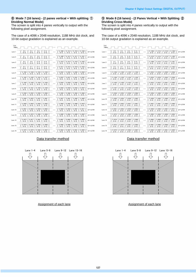
Chapter 4 Digital Output Settings (DIGITAL OUTPUT)
127
⑧ Mode 7 (16 lanes) - (2 panes vertical + With splitting ①
Dividing Normal Mode) The screen is split into 4 panes vertically to output with the following pixel assignment. The case of a 4096 x 2048 resolution, 1188 MHz dot clock, and 10-bit output gradation is explained as an example.
Data transfer method
Assignment of each lane
⑨ Mode 8 (16 lanes) - (2 Panes Vertical + With Splitting ②
Dividing Cross Mode) The screen is split into 4 panes vertically to output with the following pixel assignment. The case of a 4096 x 2048 resolution, 1188 MHz dot clock, and 10-bit output gradation is explained as an example.
Data transfer method
Assignment of each lane
・・・
[9:0] ・・・
[9:0] ・・・
[9:0] ・・・
[9:0] ・・・
[9:0] ・・・
[9:0] ・・・
[9:0] ・・・
[9:0] ・・・
L0~L2159
L0~L2159
L0~L2159
L0~L2159
L0~L2159
L0~L2159
L0~L2159
L0~L2159
CLK74MHz
Lane 1
Lane 2
Lane 3
Lane 4
Lane 5
Lane 6
Lane 7
Lane 8
[9:0] ・・・
[9:0] ・・・
[9:0] ・・・
[9:0] ・・・
[9:0] ・・・
[9:0] ・・・
[9:0] ・・・
[9:0] ・・・
L0~L2159
L0~L2159
L0~L2159
L0~L2159
L0~L2159
L0~L2159
L0~L2159
L0~L2159
Lane 9
Lane 10
Lane 11
Lane 12
Lane 13
Lane 14
Lane 15
Lane 16
D 0
D 1
D 2
D 3
D 1024
D 1025
D 1026
D 1027
D 2048
D 2049
D 2050
D 2051
D 3072
D 3073
D 3074
D 3075
[9:0]
[9:0]
[9:0]
[9:0]
[9:0]
[9:0]
[9:0]
[9:0]
[9:0]
[9:0]
[9:0]
[9:0]
[9:0]
[9:0]
[9:0]
[9:0]
D 4
D 5
D 6
D 7
D 1028
D 1029
D 1030
D 1031
D 2052
D 2053
D 2054
D 2055
D 3076
D 3077
D 3078
D 3079
[9:0]
[9:0]
[9:0]
[9:0]
[9:0]
[9:0]
[9:0]
[9:0]
[9:0]
[9:0]
[9:0]
[9:0]
[9:0]
[9:0]
[9:0]
[9:0]
D 8
D 9
D 10
D 11
D 1032
D 1033
D 1034
D 1035
D 2056
D 2057
D 2058
D 2059
D 3080
D 3081
D 3082
D 3083
[9:0]
[9:0]
[9:0]
[9:0]
[9:0]
[9:0]
[9:0]
[9:0]
[9:0]
[9:0]
[9:0]
[9:0]
[9:0]
[9:0]
[9:0]
[9:0]
D 12
D 13
D 14
D 15
D 1036
D 1037
D 1038
D 1039
D 2060
D 2061
D 2062
D 2063
D 3084
D 3085
D 3086
D 3087
[9:0]
[9:0]
[9:0]
[9:0]
[9:0]
[9:0]
[9:0]
[9:0]
[9:0]
[9:0]
[9:0]
[9:0]
[9:0]
[9:0]
[9:0]
[9:0]
D 1008
D 1009
D 1010
D 1011
D 2032
D 2033
D 2034
D 2035
D 3056
D 3057
D 3058
D 3059
D 4080
D 4081
D 4082
D 4083
[9:0]
[9:0]
[9:0]
[9:0]
[9:0]
[9:0]
[9:0]
[9:0]
[9:0]
[9:0]
[9:0]
[9:0]
[9:0]
[9:0]
[9:0]
[9:0]
D 1012
D 1013
D 1014
D 1015
D 2036
D 2037
D 2038
D 2039
D 3060
D 3061
D 3062
D 3063
D 4084
D 4085
D 4086
D 4087
[9:0]
[9:0]
[9:0]
[9:0]
[9:0]
[9:0]
[9:0]
[9:0]
[9:0]
[9:0]
[9:0]
[9:0]
[9:0]
[9:0]
[9:0]
[9:0]
D 1016
D 1017
D 1018
D 1019
D 2040
D 2041
D 2042
D 2043
D 3064
D 3065
D 3066
D 3067
D 4088
D 4089
D 4090
D 4091
[9:0]
[9:0]
[9:0]
[9:0]
[9:0]
[9:0]
[9:0]
[9:0]
[9:0]
[9:0]
[9:0]
[9:0]
[9:0]
[9:0]
[9:0]
[9:0]
D 1020
D 1021
D 1022
D 1023
D 2044
D 2045
D 2046
D 2047
D 3068
D 3069
D 3070
D 3071
D 4092
D 4093
D 4094
D 4095
Lane 1-4 Lane 9-12Lane 5-8 Lane 13-16
・・・
[9:0] ・・・
[9:0] ・・・
[9:0] ・・・
[9:0] ・・・
[9:0] ・・・
[9:0] ・・・
[9:0] ・・・
[9:0] ・・・
L0~L2159
L0~L2159
L0~L2159
L0~L2159
L0~L2159
L0~L2159
L0~L2159
L0~L2159
CLK74MHz
Lane 1
Lane 2
Lane 3
Lane 4
Lane 5
Lane 6
Lane 7
Lane 8
[9:0] ・・・
[9:0] ・・・
[9:0] ・・・
[9:0] ・・・
[9:0] ・・・
[9:0] ・・・
[9:0] ・・・
[9:0] ・・・
L0~L2159
L0~L2159
L0~L2159
L0~L2159
L0~L2159
L0~L2159
L0~L2159
L0~L2159
Lane 9
Lane 10
Lane 11
Lane 12
Lane 13
Lane 14
Lane 15
Lane 16
D 0
D 2
D 1
D 3
D 1024
D 1026
D 1025
D 1027
D 2048
D 2050
D 2049
D 2051
D 3072
D 3074
D 3073
D 3075
[9:0]
[9:0]
[9:0]
[9:0]
[9:0]
[9:0]
[9:0]
[9:0]
[9:0]
[9:0]
[9:0]
[9:0]
[9:0]
[9:0]
[9:0]
[9:0]
D 4
D 6
D 5
D 7
D 1028
D 1030
D 1029
D 1031
D 2052
D 2054
D 2053
D 2055
D 3076
D 3078
D 3077
D 3079
[9:0]
[9:0]
[9:0]
[9:0]
[9:0]
[9:0]
[9:0]
[9:0]
[9:0]
[9:0]
[9:0]
[9:0]
[9:0]
[9:0]
[9:0]
[9:0]
D 8
D 10
D 9
D 11
D 1032
D 1034
D 1033
D 1035
D 2056
D 2058
D 2057
D 2059
D 3080
D 3082
D 3081
D 3083
[9:0]
[9:0]
[9:0]
[9:0]
[9:0]
[9:0]
[9:0]
[9:0]
[9:0]
[9:0]
[9:0]
[9:0]
[9:0]
[9:0]
[9:0]
[9:0]
D 12
D 14
D 13
D 15
D 1036
D 1038
D 1037
D 1039
D 2060
D 2062
D 2061
D 2063
D 3084
D 3086
D 3085
D 3087
[9:0]
[9:0]
[9:0]
[9:0]
[9:0]
[9:0]
[9:0]
[9:0]
[9:0]
[9:0]
[9:0]
[9:0]
[9:0]
[9:0]
[9:0]
[9:0]
D 1008
D 1010
D 1009
D 1011
D 2032
D 2034
D 2033
D 2035
D 3056
D 3058
D 3057
D 3059
D 4080
D 4082
D 4081
D 4083
[9:0]
[9:0]
[9:0]
[9:0]
[9:0]
[9:0]
[9:0]
[9:0]
[9:0]
[9:0]
[9:0]
[9:0]
[9:0]
[9:0]
[9:0]
[9:0]
D 1012
D 1014
D 1013
D 1015
D 2036
D 2038
D 2037
D 2039
D 3060
D 3062
D 3061
D 3063
D 4084
D 4086
D 4085
D 4087
[9:0]
[9:0]
[9:0]
[9:0]
[9:0]
[9:0]
[9:0]
[9:0]
[9:0]
[9:0]
[9:0]
[9:0]
[9:0]
[9:0]
[9:0]
[9:0]
D 1016
D 1018
D 1017
D 1019
D 2040
D 2042
D 2041
D 2043
D 3064
D 3066
D 3065
D 3067
D 4088
D 4090
D 4089
D 4091
[9:0]
[9:0]
[9:0]
[9:0]
[9:0]
[9:0]
[9:0]
[9:0]
[9:0]
[9:0]
[9:0]
[9:0]
[9:0]
[9:0]
[9:0]
[9:0]
D 1020
D 1022
D 1021
D 1023
D 2044
D 2046
D 2045
D 2047
D 3068
D 3070
D 3069
D 3071
D 4092
D 4094
D 4093
D 4095
Lane 1-4 Lane 9-12Lane 5-8 Lane 13-16

Chapter 4 Digital Output Settings (DIGITAL OUTPUT)
128
⑩ Mode 9 (16 lanes) (Without splitting)
Output is with the following pixel assignment without splitting the screen. The case of a 4096 x 2048 resolution, 1188 MHz dot clock, and 10-bit output gradation is explained as an example.
Data transfer method
Assignment of each lane
・・・
[9:0] ・・・
[9:0] ・・・
[9:0] ・・・
[9:0] ・・・
[9:0] ・・・
[9:0] ・・・
[9:0] ・・・
[9:0] ・・・
L0~L2159
L0~L2159
L0~L2159
L0~L2159
L0~L2159
L0~L2159
L0~L2159
L0~L2159
CLK74MHz
Lane 1
Lane 2
Lane 3
Lane 4
Lane 5
Lane 6
Lane 7
Lane 8
[9:0] ・・・
[9:0] ・・・
[9:0] ・・・
[9:0] ・・・
[9:0] ・・・
[9:0] ・・・
[9:0] ・・・
[9:0] ・・・
L0~L2159
L0~L2159
L0~L2159
L0~L2159
L0~L2159
L0~L2159
L0~L2159
L0~L2159
Lane 9
Lane 10
Lane 11
Lane 12
Lane 13
Lane 14
Lane 15
Lane 16
D 0
D 1
D 2
D 3
D 4
D 5
D 6
D 7
D 8
D 9
D 10
D 11
D 12
D 13
D 14
D 15
[9:0]
[9:0]
[9:0]
[9:0]
[9:0]
[9:0]
[9:0]
[9:0]
[9:0]
[9:0]
[9:0]
[9:0]
[9:0]
[9:0]
[9:0]
[9:0]
D 16
D 17
D 18
D 19
D 20
D 21
D 22
D 23
D 24
D 25
D 26
D 27
D 28
D 29
D 30
D 31
[9:0]
[9:0]
[9:0]
[9:0]
[9:0]
[9:0]
[9:0]
[9:0]
[9:0]
[9:0]
[9:0]
[9:0]
[9:0]
[9:0]
[9:0]
[9:0]
D 32
D 33
D 34
D 35
D 36
D 37
D 38
D 39
D 40
D 41
D 42
D 43
D 44
D 45
D 46
D 47
[9:0]
[9:0]
[9:0]
[9:0]
[9:0]
[9:0]
[9:0]
[9:0]
[9:0]
[9:0]
[9:0]
[9:0]
[9:0]
[9:0]
[9:0]
[9:0]
D 48
D 49
D 50
D 51
D 52
D 53
D 54
D 55
D 56
D 57
D 58
D 59
D 60
D 61
D 62
D 63
[9:0]
[9:0]
[9:0]
[9:0]
[9:0]
[9:0]
[9:0]
[9:0]
[9:0]
[9:0]
[9:0]
[9:0]
[9:0]
[9:0]
[9:0]
[9:0]
D 4032
D 4033
D 4034
D 4035
D 4036
D 4037
D 4038
D 4039
D 4040
D 4041
D 4042
D 4043
D 4044
D 4045
D 4046
D 4047
[9:0]
[9:0]
[9:0]
[9:0]
[9:0]
[9:0]
[9:0]
[9:0]
[9:0]
[9:0]
[9:0]
[9:0]
[9:0]
[9:0]
[9:0]
[9:0]
D 4048
D 4049
D 4050
D 4051
D 4052
D 4053
D 4054
D 4055
D 4056
D 4057
D 4058
D 4059
D 4060
D 4061
D 4062
D 4063
[9:0]
[9:0]
[9:0]
[9:0]
[9:0]
[9:0]
[9:0]
[9:0]
[9:0]
[9:0]
[9:0]
[9:0]
[9:0]
[9:0]
[9:0]
[9:0]
D 4064
D 4065
D 4066
D 4067
D 4068
D 4069
D 4070
D 4071
D 4072
D 4073
D 4074
D 4075
D 4076
D 4077
D 4078
D 4079
[9:0]
[9:0]
[9:0]
[9:0]
[9:0]
[9:0]
[9:0]
[9:0]
[9:0]
[9:0]
[9:0]
[9:0]
[9:0]
[9:0]
[9:0]
[9:0]
D 4080
D 4081
D 4082
D 4083
D 4084
D 4085
D 4086
D 4087
D 4088
D 4089
D 4090
D 4091
D 4092
D 4093
D 4094
D 4095
Lane 1-16

Chapter 4 Digital Output Settings (DIGITAL OUTPUT)
129
4.4.4 V-by-One HS output setting items
Level 1 Level 2 Level 3 Setting item Setting value
V-by-One HS
Output
OFF/ON
Port1 - Port16
Sets ON/OFF for each Port.
0: OFF / 1: ON
Number Of Lanes
Sets the number of data lanes for output from V-by-One HS.
* This is in accordance with the Dotclk Mode setting in “2.1 ALL
OUTPUT”.
0: Auto
Sets the number of data lanes
automatically to match Dot Clock.
20 M to 75 MHz 1 lane
75 M to 150 MHz 2 lanes
150 M to 300 MHz 4 lanes
1: 1 lane
Outputs the same video from output channel
1 and channel 2.
2: 2 lanes
Outputs the same video from output channel
1 and channel 2.
3: 4 lanes
Outputs the same video from output channel
1 and channel 2.
4: 8 lanes
5: 16 lanes
Split
Selects the screen split method of the 4Kx2K mode and x4 mode which use the frame memory in the board.
* This is in accordance with the Split Mode setting in “2.1 ALL OUTPUT”.
When the number of lanes is 8 lanes, the following setting items are displayed.
0: 4 quarter panes output
1: 4 panes vertical output
2: 2 panes horizontal output
3: 2 panes vertical output
4: Without splitting
5: Non Dividing Mode (Mode 0 x4mode)
6: Normal Mode (Mode 1 x4mode)
7: Cross Mode (Mode 2 x4mode)
8: Dividing Normal Mode (Mode 3 x4mode)
9: Dividing Cross Mode (Mode 4 x4mode)
When the number of lanes is 16 lanes, the following setting items are displayed.
0: 4 quarter panes output + 2 panes vertical output
1: 4 panes vertical output + 2 panes vertical output
2: 4 panes horizontal output + 2 panes vertical output
3: 2 panes vertical output + 2 panes vertical output
4: 2 panes vertical output + Without splitting ① (Non Dividing Mode)
5: 2 panes vertical output + Without splitting ② (Normal Mode)
6: 2 panes vertical output + Without splitting ③ (Cross Mode)
7: 2 panes vertical output + With splitting ① (Dividing Normal Mode)
8: 2 panes vertical output + With splitting ② (Dividing Cross Mode)
9: Without splitting
A: * Not output with V-by-One HS.
Pre-Emphasis
Sets pre-emphasis.
0: 0%
1: 100%
3D Flag
Sets the 3D flag.
* “3D flag on DE active period” defined in V-by-One HS Standard
Ver.1.3 and later is supported.
“3D flag on blanking period” is not supported.
0: Disable
1: Enable
Field BET Mode
Sets Field BET Mode.
0: Disable
1: Enable
Control Mode
Sets the control method of HTPDN and LOCKN.
0: Separate
1: 1 -> 234

Chapter 4 Digital Output Settings (DIGITAL OUTPUT)
130
Level 1 Level 2 Level 3 Setting item Setting value
HTPDN Ctrl 1, 2, 3, 4
LOCHN Ctrl 1, 2, 3, 4
Controls channel 1, channel 2, channel 3, and channel 4.
0: Through
1: Low
2: High
・ When the dot clock operation mode (DotClk Mode) is Auto, the number of data lanes is switched automatically according to the
dot clock.
For details, refer to the DotClk Mode settings of “2.1ALL OUTPUT”.
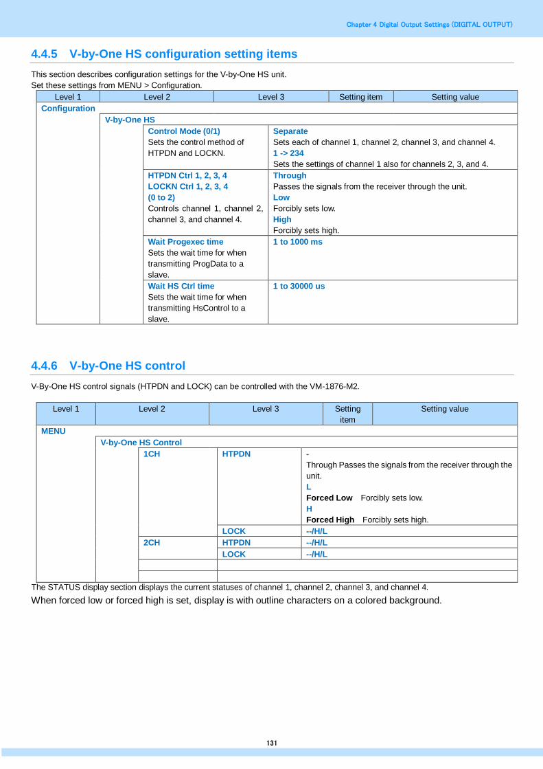
Chapter 4 Digital Output Settings (DIGITAL OUTPUT)
131
4.4.5 V-by-One HS configuration setting items
This section describes configuration settings for the V-by-One HS unit.
Set these settings from MENU > Configuration.
Level 1 Level 2 Level 3 Setting item Setting value
Configuration
V-by-One HS
Control Mode (0/1)
Sets the control method of
HTPDN and LOCKN.
Separate
Sets each of channel 1, channel 2, channel 3, and channel 4.
1 -> 234
Sets the settings of channel 1 also for channels 2, 3, and 4.
HTPDN Ctrl 1, 2, 3, 4
LOCKN Ctrl 1, 2, 3, 4
(0 to 2)
Controls channel 1, channel 2,
channel 3, and channel 4.
Through
Passes the signals from the receiver through the unit.
Low
Forcibly sets low.
High
Forcibly sets high.
Wait Progexec time
Sets the wait time for when
transmitting ProgData to a
slave.
1 to 1000 ms
Wait HS Ctrl time
Sets the wait time for when
transmitting HsControl to a
slave.
1 to 30000 us
4.4.6 V-by-One HS control
V-By-One HS control signals (HTPDN and LOCK) can be controlled with the VM-1876-M2.
Level 1 Level 2 Level 3 Setting
item
Setting value
MENU
V-by-One HS Control
1CH HTPDN -
Through Passes the signals from the receiver through the
unit.
L
Forced Low Forcibly sets low.
H
Forced High Forcibly sets high.
LOCK --/H/L
2CH HTPDN --/H/L
LOCK --/H/L
The STATUS display section displays the current statuses of channel 1, channel 2, channel 3, and channel 4.
When forced low or forced high is set, display is with outline characters on a colored background.

Chapter 4 Digital Output Settings (DIGITAL OUTPUT)
132
4.4.7 Relationship between Pattern Rendering Bit Length and Dot Clock
The dot clock is limited by the pattern rendering bit length (color depth) and dot clock operation mode (DotClk Mode) as shown in the following figures. The number of data lanes is determined by the dot clock operation mode (DotClk Mode). For details on the dot clock operation mode (DotClk Mode) and pattern bit length (color depth), refer to “2.1 ALL OUTPUT”. For details on the number of data lanes, refer to “4.4.4 V-by-One HS output setting items”. 1) When number of data lanes is 1
2) When number of data lanes is 2
3) When number of data lanes is 4
85M
シングルクロックモード
11/12Bit
9/10Bit
8Bit
ColorDepth
400MHz0.1MHz 800MHz 1200MHz 1360MHz1000MHz600MHz200MHz
20M
20M
20M
85M
75M
13/14/15/16Bit データが切り捨てられます20M 60M
40M 170M
170M
150M
シングルクロックモード
40M
40M11/12Bit
9/10Bit
8Bit
ColorDepth
400MHz0.1MHz 800MHz 1200MHz 1360MHz1000MHz600MHz200MHz
13/14/15/16Bit データが切り捨てられます120M40M
80M 340M
340M
300M
シングルクロックモード
80M
80M11/12Bit
9/10Bit
8Bit
ColorDepth
400MHz0.1MHz 800MHz 1200MHz 1360MHz1000MHz600MHz200MHz
13/14/15/16Bit 240M80M データが切り捨てられます
Single clock mode
Data is truncated.
Data is truncated.
Single clock mode
Single clock mode
Data is truncated.

Chapter 4 Digital Output Settings (DIGITAL OUTPUT)
133
4) When number of data lanes is 8
5) When number of data lanes is 16
160M 680M
680M
600M
160M
160M
デュアルクロックモード
11/12Bit
9/10Bit
8Bit
ColorDepth
400MHz0.1MHz 800MHz 1200MHz 1360MHz1000MHz600MHz200MHz
13/14/15/16Bit 160M 480M データが切り捨てられます
320M 1360M
1360M
1200M
320M
320M
クアッドクロックモード
11/12Bit
9/10Bit
8Bit
ColorDepth
400MHz0.1MHz 800MHz 1200MHz 1360MHz1000MHz600MHz200MHz
13/14/15/16Bit 320M 960M データが切り捨てられます
Dual clock mode
Quad clock mode
Data is truncated.
Data is truncated.

Chapter 4 Digital Output Settings (DIGITAL OUTPUT)
134
4.5 iTMDS unit functions and settings
The applicable unit is as follows.
4.5.1 iTMDS Unit VM-1876-M9
● Unit exterior diagram
No. Name Description
① iTMDS output Can output digital signals only. (iTMDS connectors)
Dual-Link is supported.
② Standby LED Lights when output preparation is complete. On: Normal
Off: Error (module damaged, wrong slot, etc.)
● Specifications
iTMDS
CH1
CH2
Connector DVI-I connector (x2)
Dot clock
DVI MODE 8 bit 25 to 165 MHz (Single) 50 to 330 MHz (Dual) 297 to 660 MHz (Quad) 594 to 1320 MHz (Octal)
10 bit 25 to 165 MHz (Single (16 bit)) 50 to 330 MHz (Dual (16 bit))
12 bit 25 to 165 MHz (Single (16 bit)) 50 to 320 MHz (Dual (16 bit))
16 bit 25 to 165 MHz (Single (16 bit)) 50 to 240 MHz (Dual (16 bit))
iTMDS MODE 8/10 bit 25 to 165 MHz (Single) 50 to 330 MHz (Dual) 297 to 660 MHz (Quad) 594 to 1320 MHz (Octal)
12 bit 25 to 150 MHz (Single) 50 to 300 MHz (Dual) 297 to 600 MHz (Quad) 594 to 1200 MHz (Octal)
Link Rate (R) * When iTMDS mode
R = 225 MHz (max) 8 bit: DotCLK=R, 10 bit: DotCLK=R/1.25, 12 bit: DotCLK=R/1.5
Video format RGB, YCbCr 4:4:4
E-EDID Ver. 1.3 (DDC2B) compliant
② ①

Chapter 4 Digital Output Settings (DIGITAL OUTPUT)
135
4.5.2 Connector and pin assignment
Pin No. Signal Pin No. Signal Pin No. Signal
1 TMDS DATA2- 9 TMDS DATA1- 17 TMDS DATA0-
2 TMDS DATA2+ 10 TMDS DATA1+ 18 TMDS DATA0+
3 TMDS DATA2/4 G 11 TMDS DATA1/3 G 19 TMDS DATA0/5 G
4 TMDS DATA4- 12 TMDS DATA3- 20 TMDS DATA5-
5 TMDS DATA4+ 13 TMDS DATA3+ 21 TMDS DATA5+
6 DDC CLK 14 +5 V (DDC power
supply*1) 22 TMDS CLK G
7 DDC DATA 15 GND 23 TMDS CLK+
8 Analog Vsync 16 SENSE 24 TMDS CLK-
C1 Analog Red
C2 Analog Green
C3 Analog Blue
C4 Analog Hsync
C5 Analog Ground
*1 The supply current of the DDC power supply is limited. Refer to “5.1 DDC power supply max power current
consumption”.

Chapter 4 Digital Output Settings (DIGITAL OUTPUT)
136
4.5.3 iTMDS data transfer method
● <Specifications when DVI mode output>
[Single (8 bit)]
The video is output for all two channels. Furthermore, the
output gradation is 8-bit.
The case of a 1920 x 1080p60 resolution, 148.5 MHz dot clock,
and 8-bit output gradation is explained as an example.
Data transfer method
CH1 CH2
Assignment of each lane
[Dual (8 bit)] Video is output as a combination of EVEN and OUT Furthermore, the output gradation is 8-bit. The case of a 1920 x 1080p120 resolution, 297 MHz dot clock, and 8-bit output gradation is explained as an example. Channels 1 and 2 output the same picture.
Data transfer method
CH1 CH2
Assignment of each lane
(Video 1 and Video 2 are the same picture)
(Video 3 and Video 4 are the same picture)
(Video1-EVEN / Video2-ODD)
(Video3-EVEN / Video4-ODD)

Chapter 4 Digital Output Settings (DIGITAL OUTPUT)
137
[Single (16 bit)] 16-bit video is output as a combination of the upper 8 bits and lower 8 bits for one channel. The case of outputting a 1920 x 1080p60 resolution, 148.5 MHz dot clock, 16-bit output gradation, and channel 1: 8 bits and channel 2: 8 bits is explained as an example.
Data transfer method
CH1 CH2
Assignment of each lane
[When dual (16-bit) DVI mode] 16-bit video is output by outputting the upper 8 bits from channel 1 and the lower 8 bits from channel 2. The case of outputting a 1920 x 1080p120 resolution, 297 MHz dot clock, 16-bit output gradation, and channel 1: 8 bits and channel 2: 8 bits is explained as an example.
Data transfer method
CH1 CH2
Assignment of each lane
Video 1 is upper 8 bits [15:8], Video 2 is lower 8 bits [7:0]
Video 3 is upper 8 bits [15:8], Video 4 is lower 8 bits [7:0]
Video 1 is the EVEN of upper 8 bits [15:8], Video 2 is ODD of upper 8 bits [15:8]
Video 3 is EVEN of lower 8 bits [7:0], Video 4 is ODD of lower 8 bits [7:0]

Chapter 4 Digital Output Settings (DIGITAL OUTPUT)
138
● <Specifications when iTMDS mode output>
[When dual (16-bit) iTMDS mode] Output is with EVEN and ODD as a combination for 1 channel with EVEN from Video 1 and Video 3 and ODD from Video 2 and Video 4. The case of outputting a 1920 x 1080p120 resolution, 297 MHz dot clock, and 10-bit output gradation is explained as an example.
Data transfer method
CH1 CH2
(Video1-EVEN / Video2-ODD) (Video3-EVEN / Video4-ODD)
Assignment of each lane
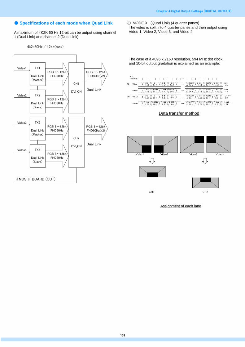
Chapter 4 Digital Output Settings (DIGITAL OUTPUT)
139
● Specifications of each mode when Quad Link A maximum of 4K2K 60 Hz 12-bit can be output using channel 1 (Dual Link) and channel 2 (Dual Link).
① MODE 0 (Quad Link) (4 quarter panes)
The video is split into 4 quarter panes and then output using Video 1, Video 2, Video 3, and Video 4.
The case of a 4096 x 2160 resolution, 594 MHz dot clock, and 10-bit output gradation is explained as an example.
Data transfer method
Assignment of each lane

Chapter 4 Digital Output Settings (DIGITAL OUTPUT)
140
② MODE 1 (Quad Link) (4 panes vertical)
The video is split into 4 panes vertically, which are assigned from the left in order of video channel 1, video channel 2, video channel 3, and video channel 4. The case of a 4096 x 2160 resolution, 594 MHz dot clock, and 10-bit output gradation is explained as an example.
Data transfer method
Assignment of each lane
③ MODE 2 (Quad Link) (2 panes horizontal)
The video of the upper half is output with ODD and EVEN using Video 1 and Video 2. The video of the lower half is output with ODD and EVEN using Video 3 and Video 4.
The case of a 4096 x 2160 resolution, 594 MHz dot clock, and 10-bit output gradation is explained as an example.
Data transfer method
Assignment of each lane

Chapter 4 Digital Output Settings (DIGITAL OUTPUT)
141
④ MODE 3 (Quad Link) (2 panes vertical)
The video of the left half is output with ODD and EVEN using Video 1 and Video 2. The video of the right half is output with ODD and EVEN using Video 3 and Video 4.
The case of a 4096 x 2160 resolution, 594 MHz dot clock, and 10-bit output gradation is explained as an example.
Data transfer method
Assignment of each lane
⑤ MODE 4 (Quad Link) (Without splitting)
EVEN is output using Video 1 and Video 2 and ODD is output using Video 3 and Video 4. The case of a 4096 x 2160 resolution, 594 MHz dot clock, and 10-bit output gradation is explained as an example.
Data transfer method
Assignment of each lane

Chapter 4 Digital Output Settings (DIGITAL OUTPUT)
142
● Specifications of each mode when x4 mode output
X4 Mode enables output at a maximum of FHD 240 Hz 10-bit by converting to LVDS (x8) with IA-1540 (iTMDS to LVDS conversion adapter). Splitting into MODE 0 to MODE 4 is additionally performed according to the method of assigning the data to Video 1 to Video 4.
① MODE0 x4 Mode (Quad Link) (Non Dividing Mode)
Video 1, Video 2, Video 3, and Video 4 are used to output with the following pixel assignment without splitting the screen. The case of a 1920 x 1080 resolution, 594 MHz dot clock, and 10-bit output gradation is explained as an example.
Data transfer method
Assignment of each lane
Conversion
adapter
Conversion
adapter

Chapter 4 Digital Output Settings (DIGITAL OUTPUT)
143
②MODE1 x4 Mode (Quad Link) (Normal Mode)
Video 1, Video 2, Video 3, and Video 4 are used to output with the following pixel assignment without splitting the screen. The case of a 1920 x 1080 resolution, 594 MHz dot clock, and 10-bit output gradation is explained as an example.
X4 Mode is an output mode for the purpose of Full HD 240 Hz compatible FPD testing. The VG output is connected to the IA-1540 (iTMDS-LVDS conversion box) to use as 8-channel output by halving the output using the conversion box. The following explanation is for the signals of 4 channels output from the VG. For an explanation of when 8-channel output from the LVDS, refer to “4.4.3 V-by-OneHS data transfer method”.
Data transfer method
Assignment of each lane
③ MODE2 x4 Mode (Quad Link) (Cross Mode)
Video 1, Video 2, Video 3, and Video 4 are used to output with the following pixel assignment without splitting the screen. The case of a 1920 x 1080 resolution, 594 MHz dot clock, and 10-bit output gradation is explained as an example.
X4 Mode is an output mode for the purpose of Full HD 240 Hz compatible FPD testing. The VG output is connected to the IA-1540 (iTMDS-LVDS conversion box) to use as 8-channel output by halving the output using the conversion box. The following explanation is for the signals of 4 channels output from the VG. For an explanation of when 8-channel output from the LVDS, refer to “4.4.3 V-by-OneHS data transfer method”.
Data transfer method
Assignment of each lane

Chapter 4 Digital Output Settings (DIGITAL OUTPUT)
144
④MODE3 x4 Mode (Quad Link) (Dividing Normal Mode)
The video of the right half is output using Video 1 and Video 2. The video of the left half is output using Video 3 and Video 4. The pixel assignment is as follows. The case of a 1920 x 1080 resolution, 594 MHz dot clock, and 10-bit output gradation is explained as an example. X4 Mode is an output mode for the purpose of Full HD 240 Hz compatible FPD testing. The VG output is connected to the IA-1540 (iTMDS-LVDS conversion box) to use as 8-channel output by halving the output using the conversion box. The following explanation is for the signals of 4 channels output from the VG. For an explanation of when 8-channel output from the LVDS, refer to “4.4.3 V-by-OneHS data transfer method”.
Data transfer method
Assignment of each lane
⑤MODE4 x4 Mode (Quad Link) (Dividing Cross Mode)
The video of the right half is output using Video 1 and Video 2. The video of the left half is output using Video 3 and Video 4. The pixel assignment is as follows. The case of a 1920 x 1080 resolution, 594 MHz dot clock, and 10-bit output gradation is explained as an example. X4 Mode is an output mode for the purpose of Full HD 240 Hz compatible FPD testing. The VG output is connected to the IA-1540 (iTMDS-LVDS conversion box) to use as 8-channel output by halving the output using the conversion box. The following explanation is for the signals of 4 channels output from the VG. For an explanation of when 8-channel output from the LVDS, refer to “4.4.3 V-by-OneHS data transfer method”.
Data transfer method
Assignment of each lane

Chapter 4 Digital Output Settings (DIGITAL OUTPUT)
145
● Specifications of each mode when Octal Link This mode enables output at a maximum of 4K2K 120 Hz 12-bit by using two of this product. Splitting into MODE 0 to MODE 9 is additionally performed according to the method of assigning the data to Video 1 to Video 8.
① MODE 0 (Octal Link) (4 quarter panes + 2 panes vertical)
This mode uses Video 1 to Video 8. The video from each output is split into 4 quarters for output then split into 2 vertically for each board and output. The case of a 4096 x 2048 resolution, 1188 MHz dot clock, and 10-bit output gradation is explained as an example.
Data transfer method
Assignment of each lane

Chapter 4 Digital Output Settings (DIGITAL OUTPUT)
146
② MODE 1 (Octal Link) (4 panes vertical + 2 panes vertical)
This mode uses Video 1 to Video 8. The video from each output is split into 4 vertically for output then split into 2 vertically for each board and output. The case of a 4096 x 2048 resolution, 1188 MHz dot clock, and 10-bit output gradation is explained as an example.
Data transfer method
Assignment of each lane
③MODE 2 (Octal Link) (2 panes horizontal + 2 panes vertical)
This mode uses Video 1 to Video 8. The video from each output is split into 2 horizontally for output then split into 2 vertically for each board and output. The case of a 4096 x 2048 resolution, 1188 MHz dot clock, and 10-bit output gradation is explained as an example.
Data transfer method
Assignment of each lane

Chapter 4 Digital Output Settings (DIGITAL OUTPUT)
147
④MODE 3 (Octal Link) (2 panes vertical + 2 panes vertical)
This mode uses Video 1 to Video 8. The video from each output is split into 2 vertically for output then split into 2 vertically for each board and output. The case of a 4096 x 2048 resolution, 1184 MHz dot clock, and 10-bit output gradation is explained as an example.
Data transfer method
Assignment of each lane
⑤ MODE 4 (Octal Link) (2 panes vertical output + Without
splitting ① (Non Dividing Mode))
This mode uses Video 1 to Video 8. The video from each output is split into 2 vertically then output with the left half output from Video 1 to Video 4 and the right half output from Video 5 to Video 8 with the following pixel assignment. The case of a 4096 x 2048 resolution, 1188 MHz dot clock, and 10-bit output gradation is explained as an example.
Data transfer method
Assignment of each lane

Chapter 4 Digital Output Settings (DIGITAL OUTPUT)
148
⑥ MODE 5 (Octal Link) (2 panes vertical output + Without
splitting ② (Normal Mode))
This mode uses Video 1 to Video 8. The video from each output is split into 2 vertically then output with the left half output from Video channel 1 to Video channel 4 and the right half output from Video channel 5 to Video channel 8 with the following pixel assignment. The case of a 4096 x 2048 resolution, 1188 MHz dot clock, and 10-bit output gradation is explained as an example.
Data transfer method
Assignment of each lane
⑦ MODE 6 (Octal Link) (2 panes vertical output + Without
splitting ③ (Cross Mode))
This mode uses Video 1 to Video 8. The video from each output is split into 2 vertically then output with the left half output from Video 1 to Video 4 and the right half output from Video 5 to Video 8 with the following pixel assignment. The case of a 4096 x 2048 resolution, 1188 MHz dot clock, and 10-bit output gradation is explained as an example.
Data transfer method
Assignment of each lane

Chapter 4 Digital Output Settings (DIGITAL OUTPUT)
149
⑧ MODE 7 (Octal Link) (2 panes vertical output + With
splitting ① (Dividing Normal Mode))
This mode uses Video 1 to Video 8. The video from each output is split into 2 vertically then output with the left half output from Video 1 to Video 4 and the right half output from Video 5 to Video 8 with the following pixel assignment. The case of a 4096 x 2048 resolution, 1188 MHz dot clock, and 10-bit output gradation is explained as an example.
Data transfer method
Assignment of each lane
⑨ MODE 8 (Octal Link) (2 panes vertical output + With
splitting ② (Dividing Cross Mode))
This mode uses Video 1 to Video 8. The video from each output is split into 2 vertically then output with the left half output from Video 1 to Video 4 and the right half output from Video 5 to Video 8 with the following pixel assignment. The case of a 4096 x 2048 resolution, 1188 MHz dot clock, and 10-bit output gradation is explained as an example.
Data transfer method
Assignment of each lane

Chapter 4 Digital Output Settings (DIGITAL OUTPUT)
150
⑩ MODE 9 (Octal Link) (Without splitting)
Channels 1 to 8 are used. Output is from each output board with the following pixel assignment without splitting. The case of a 4096 x 2048 resolution, 1188 MHz dot clock, and 10-bit output gradation is explained as an example.
Data transfer method
Assignment of each lane

Chapter 4 Digital Output Settings (DIGITAL OUTPUT)
151
4.5.4 iTMDS output setting items
Level 1 Level 2 Level 3 Setting item Setting value
iTMDS
OFF/ON Port1 to Port8
Sets ON/OFF for each Port.
0: OFF / 1: ON
iTMDS Or DVI
Sets the output signal format.
0: DVI
Outputs in DVI compatible format.
Output is single link 8-bit.
1: iTMDS
Outputs with iTMDS.
Output is single link up to 12-bit.
Mode
Sets the signal bit
length and link format
for video output from
iTMDS.
Furthermore, the same
bit length can also be
selected automatically.
・ Select single when DotClk is within the range of 25 M to 165 MHz to enable
distributed output from output channel 1 and channel 2.
・ Select dual when DotClk is within the range of 50 M to 330 MHz to enable
distributed output from output channel 1 and channel 2.
・ Select quad when DotClk is within the range of 297 M to 660 MHz to enable
distributed output from output channel 1 and channel 2.
・ Select octal when DotClk is within the range of 594 M to 1320 MHz to enable
output with a combination of Board_1_Output channel 1/channel 2 and
Board_2_Output channel 1/channel 2 by using two output boards.
0: Single (8 bit)
Outputs with single link from output channel 1 and channel 2. The portion of the bit
length of pattern rendering that exceeds 8 bits will be truncated. (Up to 12 bits
when iTMDS)
1: Dual (8 bit)
Outputs with dual link from output channel 1 and channel 2. The portion of the bit length
of pattern rendering that exceeds 8 bits will be truncated. (Up to 12 bits when iTMDS)
2: Single (16 bit)
Outputs a maximum of 16 bits with single link using the two links of master and slave of
one connector. The portion of the bit length of pattern rendering that is short of the bit
length set here will be compensated for with “0.”
Outputs the upper bits to master and the lower bits to slave.
3: Dual (16 bit)
Outputs a maximum of 16 bits with dual link using two connectors. The portion of the bit
length of pattern rendering that is short of the bit length set here will be compensated for
with “0.”
4: Single (Auto)
Outputs with single link from output channel 1 and channel 2. Automatically switches to
Single (8 bit) or Single(16 bit) according to the bit length of pattern rendering.
5: Dual (Auto)
Outputs with dual link from output channel 1 and channel 2. Automatically switches to
Dual (8bit) or Dual (16 bit) according to the bit length of pattern rendering.
6: Quad (8 bit)
Outputs with quad link using output channel 1 and channel 2. The portion of the bit length
of pattern rendering that exceeds 8 bits will be truncated. (Up to 12 bits when iTMDS)
Refer to the following “Split” item for the screen splitting method.
7: Octal (8 bit)
Outputs with octal link by using a combination of Board_1_Output channel 1/channel 2
and Board_2_Output channel 1/channel 2 by using two output boards. The portion of the
bit length of pattern rendering that exceeds 8 bits will be truncated. (Up to 12 bits when
iTMDS) Refer to the following “Split” item for the screen splitting method.
Split Uses the frame memory in the board.
When Mode is Quad, the following setting items are enabled.
0: Mode0
4 quarter panes output
1: Mode1
4 panes vertical output
2: Mode2
2 panes horizontal output

Chapter 4 Digital Output Settings (DIGITAL OUTPUT)
152
Level 1 Level 2 Level 3 Setting item Setting value
3: Mode3
2 panes vertical output
4: Mode4
No divisions
5: Mode0 (x4 Mode)
Without splitting ① (Non Dividing Mode)
6: Mode1 (x4 Mode)
Without splitting ② (Normal Mode)
7: Mode2 (x4 Mode)
Without splitting ③ (Cross Mode)
8: Mode3 (x4 Mode)
With splitting ① (Dividing Normal Mode)
9: Mode4(x4Mode)
With splitting ② (Dividing Cross Mode)
Split When Mode is Octal, the following setting items are enabled.
0: Mode0
4 quarter panes output + 2 panes vertical output
1: Mode1
4 panes vertical output + 2 panes vertical output
2: Mode2
2 panes horizontal output + 2 panes vertical output
3: Mode3
2 panes vertical output + 2 panes vertical output
4: Mode4
2 panes vertical output + Without splitting ① (Non Dividing Mode)
5: Mode5
2 panes vertical output + Without splitting ② (Normal Mode)
6: Mode6
2 panes vertical output + Without splitting ③ (Cross Mode)
7: Mode7
2 panes vertical output + With splitting ① (Dividing Normal Mode)
8: Mode8
2 panes vertical output + With splitting ② (Dividing Cross Mode)
9: Mode9
No divisions
A: Mode10
* Not output with iTMDS.
CTL0 / CTL1 This is normally not used. Leave it set to Low.
4.5.5 Polarity setting of synchronization signal
For the detailed setting procedure, refer to the Sync settings of “2.1 ALL OUTPUT”.

Chapter 4 Digital Output Settings (DIGITAL OUTPUT)
153
4.5.6 Relationship between Pattern Rendering Bit Length and Dot Clock
The dot clock is limited by the pattern rendering bit length (color depth) and dot clock operation mode (DotClk Mode) as shown in the following figures. The number of data lanes is determined by the dot clock operation mode (DotClk Mode). For details on the dot clock operation mode (DotClk Mode) and pattern bit length (color depth), refer to “2.1 ALL OUTPUT”.
1) When DVI output
When color depth > video width, data is truncated.
When color depth < video width, "0" data is added at the lower
level.
When color depth > video width, data is truncated.
When color depth < video width, "0" data is added at the lower
level.
When color depth > video width, data is truncated.
When color depth < video width, "0" data is added at the lower
level.
When color depth > video width, data is truncated.
When color depth < video width, "0" data is added at the lower
level.
Data is truncated.
Data is truncated.

Chapter 4 Digital Output Settings (DIGITAL OUTPUT)
154
2) When iTMDS output
When color depth > video width, data is truncated.
When color depth < video width, "0" data is added at the lower
level.
When color depth > video width, data is truncated.
When color depth < video width, "0" data is added at the lower
level.
When color depth > video width, data is truncated.
When color depth < video width, "0" data is added at the lower
level.
When color depth > video width, data is truncated.
When color depth < video width, "0" data is added at the lower
level.
Data is truncated.
Data is truncated.
Data is truncated.
Data is truncated.

Chapter 4 Digital Output Settings (DIGITAL OUTPUT)
155
4.6 HDBaseT unit functions and settings
The applicable unit is as follows.
4.6.1 VM-1876-MC output
● Unit exterior diagram
No. Name Description
① HDBaseT output HDBaseT signal output terminal 1 to 4. (HDCP supported)
② Standby LED Lights when output preparation is complete. On: Normal
Off: Error (module damaged, wrong slot, etc.)
① ②

Chapter 4 Digital Output Settings (DIGITAL OUTPUT)
156
● Specifications
HDBaseT
CH1
CH2
CH3
CH4
Connector HDBaseT×4
Dot Clock
*4
Single Clock Mode
<RGB/YCbCr444>
8 bit : 25 to 300 MHz
10 bit : 25 to 240 MHz
12 bit : 25 to 200 MHz
16 bit : 25 to 150 MHz
<YCbCr422>
8 bit : 25 to 300 MHz
10 bit : 25 to 300 MHz
12 bit : 25 to 300 MHz
Dual Clock Mode
*1
<RGB/YCbCr444>
8 bit : 50 to 600 MHz
10 bit : 50 to 480 MHz
12 bit : 50 to 400 MHz
16 bit : 50 to 300 MHz
<YCbCr422>
8 bit : 50 to 600 MHz
10 bit : 50 to 600 MHz
12 bit : 50 to 600 MHz
<YCbCr420>
8 bit : 50 to 600 MHz
10 bit : 50 to 480 MHz
12 bit : 50 to 400 MHz
16 bit : 50 to 300 MHz
Quad Clock Mode
*2
<RGB/YCbCr444>
8 bit : 100 to 1200 MHz
10 bit : 100 to 960 MHz
12 bit : 100 to 800 MHz
16 bit : 100 to 600 MHz
<RGB/YCbCr422>
8 bit : 100 to 1200 MHz
10 bit : 100 to 1200 MHz
12 bit : 100 to 1200 MHz
No. of colors RGB each 8/10/12/16bit(RGB/ YCbCr444/ YCbCr422/ YCbCr420)
Audio
Out HDMI
L-PCM
Sampling : 32k/ 44.1k/ 48k/ 88.2k/ 96k/ 176.4k/ 192kHz
Output Frequency: 100Hz to 20kHz
Bit number: 16/20/24bit
Compre-
ssion AC3,AAC
Option
Next generation audio *3
DSD, Dolby Digital Plus, Dolby True HD,
DTS HD (High Resolution Audio), DTS HD(Master Audio)
Copy Protection HDCP Ver1.4
Added functions E-EDID Ver1.4(DDC2B), xvYCC, CEC
*1 Uses CH1-CH2 (CH3-CH4) for parallel output. However, distributes output for YCbCr420 only.
*2 Uses CH1-CH2-CH3-CH4 for parallel output.
*3 Next-generation audio function is available when a license is purchased.
*4 TMDSCLK 3GHz

Chapter 4 Digital Output Settings (DIGITAL OUTPUT)
157
4.6.2 Connector and pin assignment
● Connector:HDBaseT
1 8
Pin No. Signal
1 TX0+
2 TX0-
3 TX1+
4 TX2+
5 TX2-
6 TX1-
7 TX3+
8 TX3-
PoE is not supported.
4.6.3 HDBaseT data transfer method
For the data transfer method of the HDMI signal output from the HDBaseT unit, see “4.1.7 HDMI data transfer method”.

Chapter 4 Digital Output Settings (DIGITAL OUTPUT)
158
4.6.4 Output setting items
This section describes output settings for the HDbaseT unit.
Level 1 Level 2 Level 3 Setting item Setting value
HDBaseT
Output
OFF/ON
Port1 to Port16
ON/OFF setting by each port.
0:OFF / 1:ON
HDMI or DVI 0:HDMI / 1:DVI / 2:Auto
Video Format: 0:RGB/ 1:YCbCr4:4:4/ 2:YCbCr4:2:2/
3:YCbYr4:2:0
Width 0:Auto / 1:8bit / 2:10bit / 3:12bit / 4:16bit
InfoFrame Auto Set
If InfoFrame Auto Set is ON, changing the Video Format will cause
the RGB or YCbCr item of AVI InfoFrame to follow and change.
0:OFF / 1:ON
Audio Output 0:OFF / 1:ON
InfoFrame/
Packet
Some items
are
automatically
set according
to the setting
of Auto
Select of the
configuration
setting.
Vendor
Specific
InfoFrame 1, 2
It is only VG-
876/877/879
that can set
two
InfoFrames.
OFF/ON 0:OFF / 1:ON
Type 1 (fixed)
Version 1 (fixed)
IEEE RegID Sel 0:Other / 1:H14b / 2:HF-VSIF
IEEE Regist. ID
byIEEE RegID Sel
Other: 6-digit Each 0 to F
H14b: 000C03 (Fixed)
HF-VSIF: C45DD8 (Fixed)
The following is only displayed when IEEE RegID Sel=Other is selected.
Payload Length 0 to 24
Payload 1-24 0x00 ~ 0xFF
The following is only displayed when IEEE RegID Sel=H14b is selected.
Video Format 0:None / 1:Ext. Resolution / 2:3D
HDMI VIC,
* Only displayed when Video
Format=Ext. Resolution is
selected.
0:4Kx2K 29.97/30Hz
1:4Kx2K 25Hz
2:4Kx2K 23.98/24Hz
3:4Kx2K 24Hz(SMPTE)
3D Structure,
* Only displayed when Video
Format=3D is selected.
The output signal differs from
the standards. The DE signal
switches to HIGH for the
current Field alternative
Vblank3 interval.
0:Frame Packing
1:Field Alternative
2:Line Alternative
3:Side-by-Side(Full)
4:L + depth
5:L + d + G + G-d
( L + depth + graphics + graphics-depth )
6:Side-by-Side(Half)
7:Top & Bottom
3D Ext Data,
1:Horizontal O/L,O/R
Horizontal sub-sampling
Odd/Left picture,Odd/Right picture
1:Horizontal O/L,E/R
Horizontal sub-sampling
Odd/Left picture,Even/Right picture
2:Horizontal E/L,O/R
Horizontal sub-sampling
Even/Left picture,Odd/Right picture
3:Horizontal E/L,E/R
Horizontal sub-sampling
Even/Left picture,Even/Right picture
4:Quincunx O/L,O/R
Quincunx matrix
Odd/Left picture,Odd/Right picture
5:Quincunx O/L,E/R
Quincunx matrix
Odd/Left picture,Even/Right picture
HDMI

Chapter 4 Digital Output Settings (DIGITAL OUTPUT)
159
Level 1 Level 2 Level 3 Setting item Setting value
HDBase
T
InfoFrame/
Packet
Vendor
Specific
InfoFrame 1, 2
3D Ext Data,
6:Quincunx E/L,O/R
Quincunx matrix
Even/Left picture,Odd/Right picture
7:Quincunx E/L,E/R
Quincunx matrix
Even/Left picture,Even/Right picture
3DMeta Present
* Only displayed when Video
Format=3D is selected.
0:0 (Not Present) / 1:1
Metadata Type
* Only displayed when Video
Format=3D is selected.
0 (fixed)
Metadata Length
* Only displayed when Video
Format=3D is selected.
0 to 21
Metadata 1-21 :
* Only displayed when Video
Format=3D is selected.
0x00 to 0xFF
The following is only displayed when IEEE RegID Sel=HF-VSIF is selected.
HF-VSIF Version 1 (fixed)
3D Valid 0 / 1
3D F Structure
* Only displayed when 3D Valid =
1 is selected.
The output signal differs from
the standards. The DE signal
switches to HIGH for the
current Field alternative
Vblank3 interval.
0:Frame Packing
1:Field Alternative
2:Line Alternative
3:Side-by-Side(Full)
4:L + depth
5:L + d + G + G-d
( L + depth + graphics + graphics-depth )
6:Side-by-Side(Half)
7:Top & Bottom
3D F Ext Data
* Only displayed when 3D Valid =
1 is selected.
3D Ext Data values “0 to 3”
are all switched to
“Horizontal sub-sampling” in
HDMI Ver.1.4a.
In VG, the previous notation
is included for distinguishing
rendering methods in OPT
Pattern 101 and
compatibility.
0:Horizontal O/L,O/R
Horizontal sub-sampling
Odd/Left picture,Odd/Right picture
1:Horizontal O/L,E/R
Horizontal sub-sampling
Odd/Left picture,Even/Right picture
2:Horizontal E/L,O/R
Horizontal sub-sampling
Even/Left picture,Odd/Right picture
3:Horizontal E/L,E/R
Horizontal sub-sampling
Even/Left picture,Even/Right picture
4:Quincunx O/L,O/R
Quincunx matrix
Odd/Left picture,Odd/Right picture
5:Quincunx O/L,E/R
Quincunx matrix
Odd/Left picture,Even/Right picture
3D F Ext Data 6:Quincunx E/L,O/R
Quincunx matrix
Even/Left picture,Odd/Right picture
7:Quincunx E/L,E/R
Quincunx matrix
Even/Left picture,Even/Right picture
Additional Pre
* Only displayed when 3D Valid =
1 is selected.
0(Not Present) / 1

Chapter 4 Digital Output Settings (DIGITAL OUTPUT)
160
Level 1 Level 2 Level 3 Setting item Setting value
HDBase
T
InfoFrame/
Packet
Vendor
Specific
InfoFrame 1, 2
Dual View
* Only displayed when 3D Valid =
1 is selected.
0:Normal 3D/ 1:Dual View
View Dependency
* Only displayed when 3D Valid =
1 is selected.
0:No Indication
1:Right Originate
2:Left Originate
3:Both
Preferred 2D
* Only displayed when 3D Valid =
1 is selected.
0:No Indication
1:Right View
2:Left View
Disparity Pre
* Only displayed when 3D Valid =
1 is selected.
0(Not Present) / 1
Disparity Ver
* Only displayed when 3D Valid =
1 is selected.
0 to 3
Disparity Length
* Only displayed when 3D Valid =
1 is selected.
Disparity Ver = 0
Length = 0
Disparity Ver = 1
Length = 3
Disparity Ver = 2
Disparity Data1 = 2h : Length = 3
Disparity Data1 = 3h : Length = 4
Disparity Data1 = 4h : Length = 5
Disparity Data1 = 5h : Length = 6
Disparity Data1 = ah : Length = 11
Disparity Data1 = 11h : Length = 18
Disparity Data1 = else : Length = 1
Disparity Ver = 3 のとき
Disparity Data4 = 0h : Length = 4
Disparity Data4 = 2h : Length = 6
Disparity Data4 = 3h : Length = 7
Disparity Data4 = 4h : Length = 8
Disparity Data4 = 5h : Length = 9
Disparity Data4 = ah: Length = 14
Disparity Data4 = else : Length = 4
Disparity Data 1~20
* Only displayed when 3D Valid =
1 is selected.
00h to FFh
Meta Present
* Only displayed when 3D Valid =
1 is selected.
0(Not Present) / 1
Metadata Type
* Only displayed when 3D Valid =
1 is selected.
0 (fixed)
Metadata Length
* Only displayed when 3D Valid =
1 is selected.
Because VSI InfoFrame is a
maximum of 27 bytes, the
maximum Length relies on other
Data length.
0 to 20
Metadata Data 1~20,
* Only displayed when 3D Valid
= 1 is selected.
Because VSI InfoFrame is a
maximum of 27 bytes, the
maximum Length relies on other
Data length.
00h to FFh

Chapter 4 Digital Output Settings (DIGITAL OUTPUT)
161
Level 1 Level 2 Level 3 Setting item Setting value
HDBase
T
InfoFrame/
Packet
AVI InfoFrame OFF/ON 0:OFF / 1:ON
Type : 2 (fixed)
Version : 1 to 3
Scan Info 0:No Data
1:Overscanned
2:Underscanned
Bar Info 0:Data Not Valid
1:Vertical Valid
2:Horizontal Valid
3:Vert.&Horiz. Valid
ActiveF Info 0:No Data / 1:Valid
RGB or YCbCr 0:RGB
1:YCbCr 4:2:2
2:YCbCr 4:4:4
3:YCbCr 4:2:0
4:(reserved1)
5:(reserved2)
6:(reserved3)
7:IDO-Defined
ActiveF Aspect 0:Same Picture
1:4:3(center)
2:16:9(center)
3:14:9(center)
4:box 16:9(top)
5:box 14:9(top)
6:box>16:9(center)
7:4:3(14:9 center)
8:16:9(14:9 center)
9:16:9(4:3 center)
Picture Aspect 0:No Data / 1:4:3 / 2:16:9
Scaling 0:Unknown
1:Horizontal
2:Vertical
3:Horiz. & Vert.
Colorimetry 0:No Data
1:SMPTE170M/ITU601
2:ITU709
3:Extended Valid
Video Code : 0 to 107
Repetition : 1 to 10
Top Bar : 0 to 65535
Sets Line Number of End of Top Bar.
(Sets letter BOX upper Bar size.)
Bottom Bar : 0 to 65535
Sets Line Number of Start of Bottom Bar.
(Sets letter BOX lower Bar size.)
Left Bar : 0 to 65535
Sets Pixel Number of End of Left Bar.
(Sets pillar BOX left side Bar size.)
Right Bar : 0 to 65535
Sets Pixel Number of Start of Right Bar.
(Sets pillar BOX right side Bar size.)
RGB Quan.Range 0:Default
1:Limited Range
2:Full Range
YCC Quan.Range 0:Limited Range / 1:Full Range

Chapter 4 Digital Output Settings (DIGITAL OUTPUT)
162
Level 1 Level 2 Level 3 Setting item Setting value
HDBase
T
InfoFrame/
Packet
AVI InfoFrame
Extended Colorimetry
Referenced when Extended
Valid is set in Colorimetry.
0:xvYCC601
1:xvYCC709
2:sYCC601
3:AdobeYCC601
4:AdobeRGB
5:BT2020 YcCbcCrc
6:BT2020 RGBorYCbCr
IT content 0:No Data / 1:IT content
IT contentType 0:Graphics
1:Photo
2:Cinema
3:Game
SPD
InfoFrame
OFF/ON 0:OFF / 1:ON
Type : 3 (fixed)
Version : 1 (fixed)
Vendor Name : Max. 8 characters
(0x20 to 0x7E ASCII 7bit)
Product Description: Max. 16 characters
(0x20 to 0x7E ASCII 7bit)
Source Device 0:Unknown
1:Digital STB
2:DVD player
3:D-VHS
4:HDD Video recorder
5:DVC
6:DSC
7:Video CD
8:Game
9:PC general
A:Blu-Ray Disc
B:Super Audio CD
C:HD DVD
D:PMP
Audio
InfoFrame
OFF/ON 0:OFF / 1:ON
Type : 4 (fixed)
Version : 1 (fixed)
Coding Type 0:Refer Stream Header
1:IEC60958 PCM
2:AC-3
3:MPEG1(Layers 1&2)
4:MP3(MPEG1 Layer 3)
5:MPEG2(multi ch.)
6:AAC
7:DTS
8:ATRAC
9:One Bit Audio
A:Dolby Digital+
B:DTS-HD
C:MLP
D:DST
E:WMA Pro
F:Refer Extension
Coding ExtType 0:(not use1)
1:(not use2)
2:(not use3)
3:HE-AAC
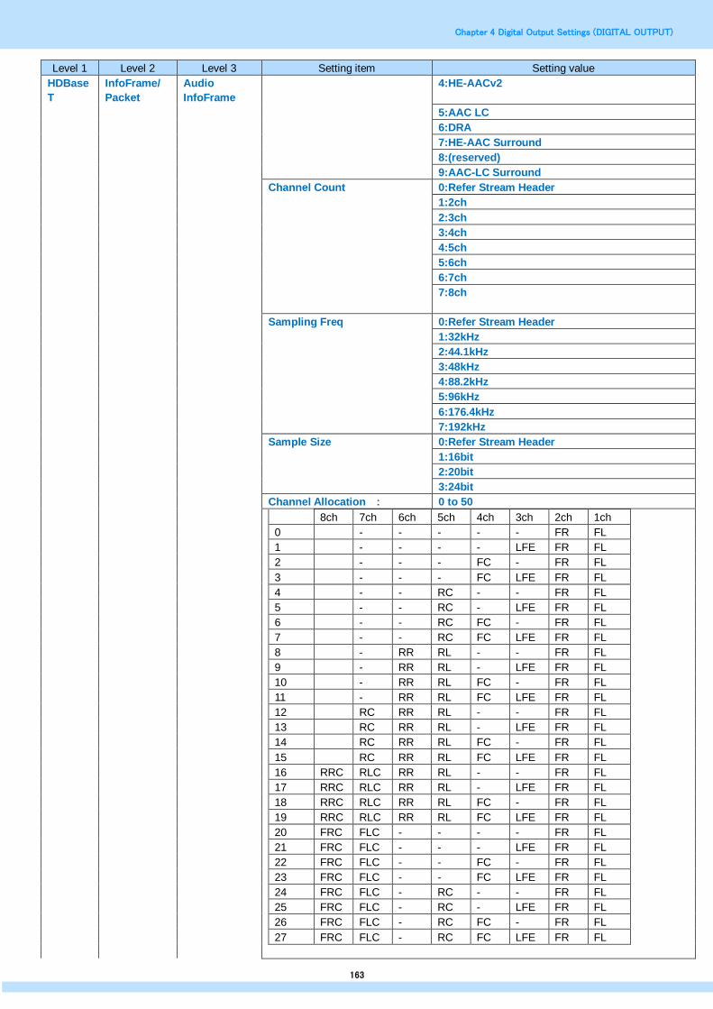
Chapter 4 Digital Output Settings (DIGITAL OUTPUT)
163
Level 1 Level 2 Level 3 Setting item Setting value
HDBase
T
InfoFrame/
Packet
Audio
InfoFrame
4:HE-AACv2
5:AAC LC
6:DRA
7:HE-AAC Surround
8:(reserved)
9:AAC-LC Surround
Channel Count 0:Refer Stream Header
1:2ch
2:3ch
3:4ch
4:5ch
5:6ch
6:7ch
7:8ch
Sampling Freq 0:Refer Stream Header
1:32kHz
2:44.1kHz
3:48kHz
4:88.2kHz
5:96kHz
6:176.4kHz
7:192kHz
Sample Size 0:Refer Stream Header
1:16bit
2:20bit
3:24bit
Channel Allocation : 0 to 50
8ch 7ch 6ch 5ch 4ch 3ch 2ch 1ch
0 - - - - - FR FL
1 - - - - LFE FR FL
2 - - - FC - FR FL
3 - - - FC LFE FR FL
4 - - RC - - FR FL
5 - - RC - LFE FR FL
6 - - RC FC - FR FL
7 - - RC FC LFE FR FL
8 - RR RL - - FR FL
9 - RR RL - LFE FR FL
10 - RR RL FC - FR FL
11 - RR RL FC LFE FR FL
12 RC RR RL - - FR FL
13 RC RR RL - LFE FR FL
14 RC RR RL FC - FR FL
15 RC RR RL FC LFE FR FL
16 RRC RLC RR RL - - FR FL
17 RRC RLC RR RL - LFE FR FL
18 RRC RLC RR RL FC - FR FL
19 RRC RLC RR RL FC LFE FR FL
20 FRC FLC - - - - FR FL
21 FRC FLC - - - LFE FR FL
22 FRC FLC - - FC - FR FL
23 FRC FLC - - FC LFE FR FL
24 FRC FLC - RC - - FR FL
25 FRC FLC - RC - LFE FR FL
26 FRC FLC - RC FC - FR FL
27 FRC FLC - RC FC LFE FR FL

Chapter 4 Digital Output Settings (DIGITAL OUTPUT)
164
Level 1 Level 2 Level 3 Setting item Setting value
HDBase
T
InfoFrame/
Packet
Audio
InfoFrame
28 FRC FLC RR RL - - FR FL
29 FRC FLC RR RL - LFE FR FL
30 FRC FLC RR RL FC - FR FL
31 FRC FLC RR RL FC LFE FR FL
32 - FCH RR RL FC - FR FL
33 - FCH RR RL FC LFE FR FL
34 TC - RR RL FC - FR FL
35 TC - RR RL FC LFE FR FL
36 FRH FLH RR RL - - FR FL
37 FRH FLH RR RL - LFE FR FL
38 FRW FLW RR RL - - FR FL
39 FRW FLW RR RL - LFE FR FL
40 TC RC RR RL FC - FR FL
41 TC RC RR RL FC LFE FR FL
42 FCH RC RR RL FC - FR FL
43 FCH RC RR RL FC LFE FR FL
44 TC FCH RR RL FC - FR FL
45 TC FCH RR RL FC LFE FR FL
46 FRH FLH RR RL FC - FR FL
47 FRH FLH RR RL FC LFE FR FL
48 FRW FLW RR RL FC - FR FL
49 FRW FLW RR RL FC LFE FR FL
50 Reserved
Level Shift Value : 0 to 15 [dB]
Down-mix 0:Permitted/No Info
1:Prohibited
LFE PB Level 0:Unknown
1:0dB Playback
2:+10dB Playback
MPEG
InfoFrame
NTSC
VBI
InfoFrame
OFF/ON 0:OFF / 1:ON
Type : 5 (fixed)
Version : 1 (fixed)
Bit Rate : 0 to 4294M967k295 [Hz]
Field Repeat 0:New Field(picture)
1:Repeated Field
Frame 0:Unknown(No Data)
1:I Picture
2:B Picture
3:P Picture
NTSC
VBI
InfoFrame
OFF/ON 0:OFF / 1:ON
Type : 6 (fixed)
Version : 1 (fixed)
PES Length : 0 ~ 27
PES 1-27 : 0x0 ~ 0xFF
Dynamic
Range and
Mastering
InfoFrame
OFF/ON 0:OFF / 1:ON
Type : 7 (fixed)
Version : 1 (fixed)
EOTF 0:SDR Range
1:HDR Range
2:SMPTE ST2084[2]
3:Future EOTF
Metadata ID Metadata Type1 (fixed)
Disp Primaries x0 0.00000 to 1.00000 (0.00002Step)
Disp Primaries y0 0.00000 to 1.00000 (0.00002Step)
Disp Primaries x1 0.00000 to 1.00000 (0.00002Step)
Disp Primaries y1 0.00000 to 1.00000 (0.00002Step)

Chapter 4 Digital Output Settings (DIGITAL OUTPUT)
165
Level 1 Level 2 Level 3 Setting item Setting value
HDBase
T
InfoFrame/
Packet
Disp Primaries x2 0.00000 to 1.00000 (0.00002Step)
Disp Primaries y2 0.00000 to 1.00000 (0.00002Step)
White Point x 0.00000 to 1.00000 (0.00002Step)
White Point y 0.00000 to 1.00000 (0.00002Step)
Max Disp Mastering 1 to 65535
Min Disp Mastering 0.0001 to 6.5535
Content Light LV 1 to 65535
Frame-ave Light LV 1 to 65535
ACP Packet
OFF/ON 0:OFF / 1:ON
ACP_Type 0:Generic Audio
1:IEC60958 Audio
2:DVD-Audio
3:Super Audio CD
DVD-Audio_Type 0 – 1
Copy Permission 0:Copy Freely
1:(reserved)
2:Specify Copy Number
3:No More Copies
Copy_Number 0:1 copies
1:2 copies
2:4 copies
3:6 copies
4:8 copies
5:10 copies
6:3 copies
7:Copy One Generation
Quality: 0 to 3
Number of CH Sampling frequency Bit Width
0 2 ch or less 48kHz or lower 16 bit or less
1 2 ch or less No restrictions No restrictions
2 No restrictions No restrictions No restrictions
3 No restrictions 48kHz or lower 16 bit or less
Transaction (0/1): 0:Not Present / 1:(reserved)
Count_A :
Count_S :
Count_U :
0 to 255
CCI_Flags Q_A (0/1):
Q_S (0/1):
Q_U (0/1):
0:CD Quality / 1:Unlimited DSD Qual
CCI_Flags Move_A (0/1):
Move_S (0/1):
Move_U (0/1):
0:Not Allowed / 1:Allowed
ISRC Packet OFF/ON ISRC1 (0/1):
ISRC2 (0/1):
0:OFF / 1:ON
ISRC_Cont (0/1): 0 to 1
ISRC_Valid (0/1): 0 to 1
ISRC_Status (0-2): 0:Starting
1:Intermediate
2:Ending
Validity Info (0-3): 0:No Validity
1:ISRC
2:UPC/EAN
3:UPC/EAN and ISRC
Catalogue Code : 13-digit Each 0 to 9
Country Code : 2 characters 0x11 to 0x2A
(ASCII upper-case characters - 0x30)
First Owner Code : 3 characters 0x00 to 0x09, 0x11 to 0x2A
(ASCII upper-case characters/numerals - 0x2A)

Chapter 4 Digital Output Settings (DIGITAL OUTPUT)
166
Level 1 Level 2 Level 3 Setting item Setting value
HDBase
T
InfoFrame/
Packet
ISRC Packet Year Of Rec. Code : 3-digit Each 0 to 9
Recording-item Code: 5-digit Each 0 to 9
Gamut
Metadata
Packet
OFF/ON (0/1): 0:OFF / 1:ON
Next_Field (0/1): 0 to 1
No_Current_GBD(0/1): 0 to 1
GBD_profile (0-3): 0:P0 / 1:P1 / 2:P2 / 3:P3
AffectedGamutSeqNum: 0 to 15
Current_GamutSeqNum: 0 to 15
Packet_Seq (0-3): 0:Intermediate
1:First
2:Last
3:Only
Format_Flag (0/1): 0:Vertices/Facets / 1:Range
ColorPrecision(0-2): 0:8bit / 1:10bit / 2:12bit
Color_Space (0-3): Format_Flag=Vertices/Facets
0:ITU-R BT.709
1:xvYCC601
2:xvYCC709
3:XYZ
Format_Flag=Range
0:Reserved
1:xvYCC601
2:xvYCC709
3:Reserved
Number_Vertices :
It is displayed only when
selecting
“Format_Flag=Vertices/Facets”.
Follows the setting of Color Precision.
8bit : 4 to 8
10bit: 4 to 6
12bit: 4 to 5
Packed_GBD_Vertices_Data
It is displayed only when
selecting
“Format_Flag=Vertices/Facets”.
DATA 1 Follows the setting of Color
Precision
8bit : 0 - 255
10bit : 0 - 1023
12bit : 0 - 4095
DATA 2
DATA 3
DATA 4
Packed_Range_Data
It is displayed only when
selecting”Format_Flag=Range”.
Min_Red Follows the setting of Color
Precision
8bit :
-3.96875 - +3.96875
10bit:
-3.9921875 - +3.9921875
12bit:
-3.998046875 - +3.998046875
Max_Red
Min_Green
Max_Green
Min_Blue
Max_Blue

Chapter 4 Digital Output Settings (DIGITAL OUTPUT)
167
4.6.5 HDBaseT Config Setting Item
This section describes how to configure the HDBaseT unit.
Set it from MENU> Configuration.
Level1 Level2 Level3 Setting
Item
Setting value
Configuration
HDBaseT
Auto Select
Send appropriate value of the following
InfoFrame automatically.
0:OFF / 1:ON
・When Program Data is saved when AutoSelect is ON, the value set by automatic selection is sent.
・For the notation "-", use the value of the original setting.
Item Setting Value / Reference Source
AVI InfoFrame
AFD Pattern is being displayed. Except the left.
Active Format Information Valid -
Active Format Aspect Follow the setting of AFD> Type. -
Top Bar The calculated value from the setting of AFD,Timing. -
Bottom Bar
Left Bar
Right Bar
RGB or YCbCr Follow the setting of HDBaseT> Video Format.
Picture Aspect Follow the setting of HDBaseT> AVI InfoFrame> Video Code. (EIA/CEA-
861 conformed)
Repetition Follow the setting of H-Timing> Repetition.
Audio InfoFrame
Follow the setting of Digital Audio> Source.
Ext.ANALOG to
L-PCM
Int.L-PCM
Ext.I2S L-PCM
(Option)
Ext.ANALOG to DSD Int.DSD
(Option)
Except
the left.
Sampling Frequency - 44.1kHz Follow the information of
DSD File.
-
Channel Count Follow the channel number that is set as “ON” in Digital Audio>
Output Channel.
0 1 2 to 8
Refer Stream Header 2ch 2 to 8ch
-
ACP Packet
Follow the setting of ACP Packet> ACP_Type.
DVD-Audio Except the left
DVD-Audio_Type 1 0
Copy_Permission - 0 (Copy Freely)
Copy_Number - 0 (1 copies)
Quality - 0

Chapter 4 Digital Output Settings (DIGITAL OUTPUT)
168
Level1 Level2 Level3 Setting
Item
Setting value
Transaction - 0 (Not Present)
ISRC Packet
Follow the setting of ACP Packet> ACP_Type.
DVD-Audio Except the left.
OFF/ON ISRC1 - OFF
ISRC2 Follow the setting of ISRC Packet>
ISRC_Cont.
0 1
OFF -
OFF
HDBaseT Packet Changing
0:Normal Mode
Disconnect the Sync of HDMI
output, and change
InfoFrame/Packet.
1:Game Mode
Change InfoFrame/Packet.
(without disconnecting Sync.)
Link Mode 0:HDBaseT Mode
Set normal HDBaseT output
mode.
1:Long Reach Mode
This is the setting which can
support cable length up to 150m.
*1
*1 “Long Reach Mode” supports up to 148.5MHz HDMI pixel clock.
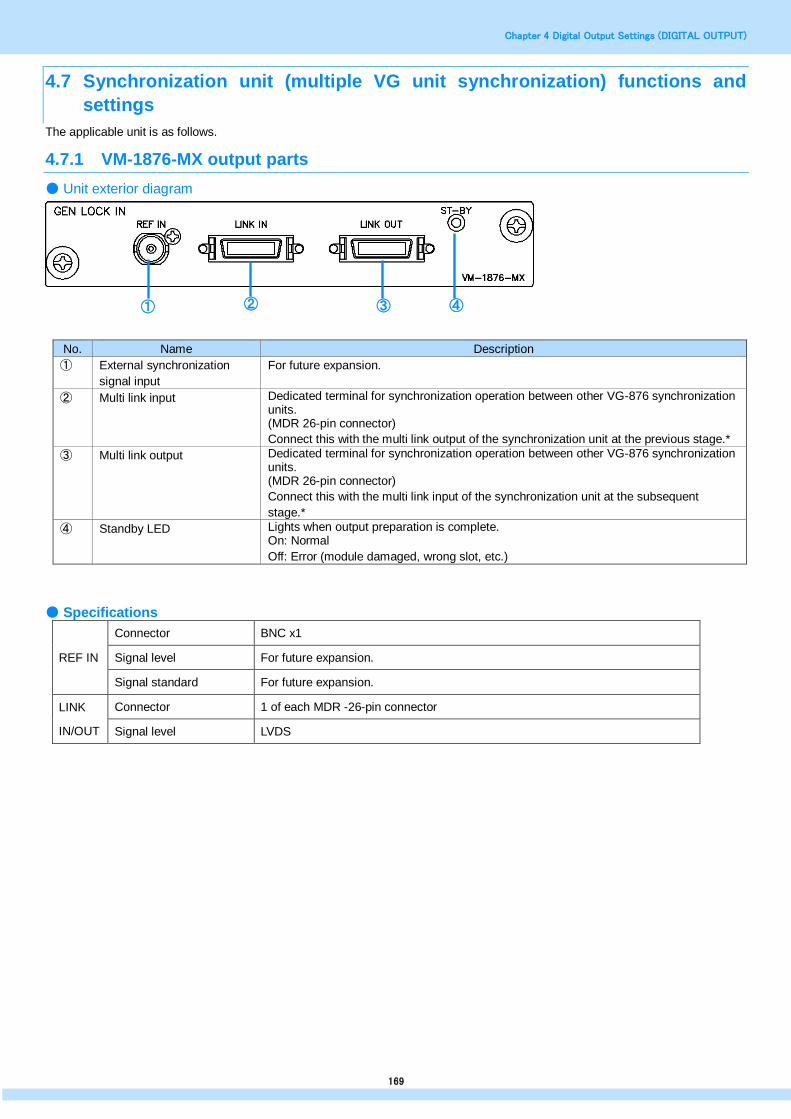
Chapter 4 Digital Output Settings (DIGITAL OUTPUT)
169
4.7 Synchronization unit (multiple VG unit synchronization) functions and
settings
The applicable unit is as follows.
4.7.1 VM-1876-MX output parts
● Unit exterior diagram
No. Name Description
① External synchronization
signal input
For future expansion.
② Multi link input Dedicated terminal for synchronization operation between other VG-876 synchronization units. (MDR 26-pin connector)
Connect this with the multi link output of the synchronization unit at the previous stage.*
③ Multi link output Dedicated terminal for synchronization operation between other VG-876 synchronization units. (MDR 26-pin connector)
Connect this with the multi link input of the synchronization unit at the subsequent
stage.*
④ Standby LED Lights when output preparation is complete. On: Normal
Off: Error (module damaged, wrong slot, etc.)
● Specifications
REF IN
Connector BNC x1
Signal level For future expansion.
Signal standard For future expansion.
LINK
IN/OUT
Connector 1 of each MDR -26-pin connector
Signal level LVDS
① ② ③ ④
Configuration

Chapter 4 Digital Output Settings (DIGITAL OUTPUT)
170
4.7.2 Overview of synchronization operation
Signals of a resolution such as 8K4K@60p that is higher than one VG unit support can be output by performing the operation to synchronize multiple units by using a synchronization unit. As an example, the following shows an image of the operation for synchronizing four units.
《8K4K@60p with HDMI output by linking 4 units》
* VM-1876-MX is installed in the IF IN slot of the VG unit.
VG-876
VM-1876A-M0
VM-1876-MX
IF OUT
IF IN
VG-876
VM-1876A-M0
VM-1876-MX
IF OUT
IF IN
VG-876
VM-1876A-M0
VM-1876-MX
IF OUT
IF IN
VG-876
VM-1876A-M0
VM-1876-MX
IF OUT
IF IN
REF
Master
REF
REF
HDMI×4
HDMI×4
HDMI×4
HDMI×4
8K4Kモニター8K4K@60p
出力映像4K2K@60p
Output video
8K4K monitor

Chapter 4 Digital Output Settings (DIGITAL OUTPUT)
171
4.7.3 Connection method
The following shows an image of connecting the multi link connectors. ● VG unit connection diagram The master and slave devices are connected by LAN (straight cable) via a hub. For details on how to set the master and slave devices, refer to “4.7.7 Synchronization unit setting items”.
● VM-1876-MX connection diagram
VM-1876-MX
ST-BY
REF IN
GENLOCK IN
LINK IN LINK OUT
VM-1876-MX
ST-BY
REF IN
GENLOCK IN
LINK IN LINK OUT
VM-1876-MX
ST-BY
REF IN
GENLOCK IN
LINK IN LINK OUT
MDRケ
ーブル
MDRケ
ーブル
同期信号
発生器CS
※未対応
Master
Slave1
Slave2
VM-1876-MX
ST-BY
REF IN
GENLOCK IN
LINK IN LINK OUT
Slave3
MDRケ
ーブル
Straight
*Not supported
Synchronization
signal generator

Chapter 4 Digital Output Settings (DIGITAL OUTPUT)
172
4.7.4 Image of splitting method when synchronizing 4 units
The screen split methods that can be supported when synchronizing 4 VG units are as follows.
For the dot clock and bit length area that can be output, refer to “Relationship between Pattern Rendering Bit Length and Dot
Clock” included in the section for each unit.
The supported units are as follows.
・ VM-1876A-M0 ・ VM-1876-M2 ・ VM-1876-M5
・ VM-1876A-M6 ・ VM-1876-M7 ・ VM-1876-M8
《VM-1876A-M0, VM-1876-M7》
* Dual clock mode is not supported.
Split Mode
*Modes 1 and 3 to
10 are not
supported.
DotClk
ModePattern image
Mode0,2
(H2/V2Div)Quad
Multi
VGMode
H2/V2Div
Pattern imageMulti
VGMode
V4Div
CH1 CH2
CH3 CH4
*1 Connector Output:1920x1080 60Hz or 120Hz 2048x1080 60Hz or 120Hz(Set any value for VIC.)
Position1 Position2
Position3 Position4

Chapter 4 Digital Output Settings (DIGITAL OUTPUT)
173
《VM-1876-M2》
● Number of Lane = 8 lanes x 4 (8K4K 60Hz)
Split
Mode
DotClk
ModePattern image
Mode0
Mode1
Mode2
Multi
VGMode
H2/V2Div
Pattern imageMulti
VGMode
Mode3,8,9
Mode4,5,6,7
Dual
(8 lanes x 4)
*Output of CH3 and CH4 is the same as that of CH1 and CH2
V4Div
1/2lane 3/4lane
5/6lane 7/8lane
1/2lane 3/4lane 5/6lane 7/8lane
1/2/3/4lane
5/6/7/8lane
1/2/3/4lane 5/6/7/8lane
1/2/・・・/7/8lane
Position1 Position2 Position3 Position4Position1 Position2
Position3 Position4
Position1 Position2
Position3 Position4
Position1 Position2 Position3 Position4
Position1 Position2
Position3 Position4
Position1 Position2
Position3 Position4
Position1 Position2
Position3 Position4
Position1 Position2 Position3 Position4
Position1 Position2 Position3 Position4
Position1 Position2 Position3 Position4

Chapter 4 Digital Output Settings (DIGITAL OUTPUT)
174
● Number of Lane = 16 lanes x 4 (8K4K 120Hz)
Split
Mode
*Mode 10 is
not supported.
DotClk Mode
Mode0
Mode1
Mode2
Pattern image
Mode3,7,8
Mode4,5,6
1/2lane
3/4lane
5/6lane
7/8lane
9/10
lane
11/12
lane
13/14
lane
15/16
lane
1/2
lane
3/4
lane
5/6
lane
7/8
lane
9/10
lane
11/12
lane
13/14
lane
15/16
lane
1/2/3/4lane 9/10/11/12lane
5/6/7/8lane 13/14/15/16lane
1/2/3/4
lane
5/6/7/8
lane
9/10/11/
12lane
13/14/15
/
16lane
Mode9
Quad
(16 Lanes x 4)
1/2/・・・/7/8
lane
9/10/・・・/15/16
lane
CH1/2/3/4
Pattern image
Position1 Position2
Position3 Position4
Position1 Position2
Position3 Position4
Position1 Position2 Position3 Position4
Position1 Position2 Position3 Position4
Position1 Position2 Position3 Position4Position1 Position2
Position3 Position4
Position1 Position2
Position3 Position4
Position1 Position2 Position3 Position4
Position1 Position2
Position3 Position4
Position1 Position2 Position3 Position4
Position1 Position2
Position3 Position4
Position1 Position2 Position3 Position4
Multi
VGMode
Multi
VGMode
H2/V2Div V4Div

Chapter 4 Digital Output Settings (DIGITAL OUTPUT)
175
《VM-1876-M5》
* Dual clock mode is not supported.
《VM-1876A-M6, VM-1876-M8》
* Quad clock mode is not supported.
Split Mode
*Modes 1 to 9 are
not supported.
DotClk
ModePattern image
Mode0
(4Square)
Quad
Mode10
(2SI)
Multi
VGMode
H2/V2Div
Pattern imageMulti
VGMode
V4Div
CH1 CH2
CH3 CH4
CH1/2/3/4
2-SAMPLE INTERLEAVE
DIVISION
*1 Connector Output:1920x1080 60Hz 2048x1080 60Hz
*1 Connector Output:1920x1080 60Hz 2048x1080 60Hz
Position1 Position2
Position3 Position4
Position1 Position2
Position3 Position4
Split Mode
*Modes 0, 2, and 4
to 9 are not
supported.
DotClk
ModePattern image
DualMode1,3
(VDiv)
Multi
VGMode
H2/V2Div
Pattern imageMulti
VGMode
V4Div
CH1
*1 Connector Output:3840x2160 60Hz 4096x2160 60Hz(Set any value for VIC.)
Position1 Position2
Position3 Position4
* 1 connector output: 1920 x 1080 60 Hz 2048 x 1080 60 Hz

Chapter 4 Digital Output Settings (DIGITAL OUTPUT)
176
4.7.5 Image of splitting method when synchronizing 2 units
The screen split methods that can be supported when synchronizing 2 VG units are as follows. For the dot clock and bit length area that can be output, refer to “Relationship between Pattern Rendering Bit Length and Dot Clock” included in the section for each unit. The supported units are as follows.
・ VM-1876A-M0 ・ VM-1876-M2 ・ VM-1876-M7
《VM-1876A-M0, VM-1876-M7》
* Dual clock mode is not supported.
Split Mode
*Modes 1 and 3 to
10 are not
supported.
DotClk
ModePattern image
Mode0,2
(H2/V2Div)Quad
Multi
VGMode
V2Div
CH1 CH2
CH3 CH4
*1 Connector Output:1920x1080 60Hz or 120Hz 2048x1080 60Hz or 120Hz(Set any value for VIC.)
*Positions 3 and 4 cannot be set.
Position1 Position2

Chapter 4 Digital Output Settings (DIGITAL OUTPUT)
177
《VM-1876-M2》
* Dual clock mode is not supported. ● Number of Lane = 16 lanes x 2 (8K4K 60Hz)
Split
Mode
*Mode 10 is
not supported.
DotClk Mode Pattern image
Mode0
Mode1
Mode2
Multi
VGMode
Mode3,7,8
Mode4,5,6
1/2lane
3/4lane
5/6lane
7/8lane
9/10
lane
11/12
lane
13/14
lane
15/16
lane
1/2
lane
3/4
lane
5/6
lane
7/8
lane
9/10
lane
11/12
lane
13/14
lane
15/16
lane
1/2/3/4lane 9/10/11/12lane
5/6/7/8lane 13/14/15/16lane
1/2/3/4
lane
5/6/7/8
lane
9/10/11/
12lane
13/14/15
/
16lane
Mode9
1/2/・・・/7/8
lane
9/10/・・・/15/16
lane
*Positions 3 and 4 cannot be set.
V2DivQuad
(16 Lanes x 2)
1/2/・・・/15/16lane
Position1 Position2
Position1 Position2
Position1 Position2
Position1 Position2
Position1 Position2
Position1 Position2

Chapter 4 Digital Output Settings (DIGITAL OUTPUT)
178
4.7.6 Scanning direction image
The scanning direction set in the Reverse Mode settings of Config is shown below.
An independent scanning direction can be set for each unit.
The following is the case when the same scanning direction is set for all four units.
● 《Multi VGMode = H2V2Div (4 quarter panes)》 ● Reverse Mode = No Reverse
● Reverse Mode = Left Right
● Reverse Mode = Top Bottom
● Reverse Mode = LR & TB
● 《Multi VGMode = V4Div (4 panes vertical)》 ● Reverse Mode = No Reverse
● Reverse Mode = Left Right

Chapter 4 Digital Output Settings (DIGITAL OUTPUT)
179
● Reverse Mode = Top Bottom
● Reverse Mode = LR & TB
● 《Multi VGMode = V2Div (2 panes vertical)》 ● Reverse Mode = No Reverse
● Reverse Mode = Left Right
● Reverse Mode = Top Bottom
● Reverse Mode = LR & TB

Chapter 4 Digital Output Settings (DIGITAL OUTPUT)
180
4.7.7 Synchronization unit setting items
《VM-1876-MX Setting Parameters》
Level 1 Level 2 Level 3 Setting item Setting value
Mode
0: OFF
Does not operate in the synchronization mode.
1: Master
Operates in the synchronization mode as the master device.
2: Slave
Operates in the synchronization mode as a slave device.
Position
Sets the drawing position of the VG. * This is dependent on the Multi VGMode setting of All Output. * Please do not set this to Position 3 and Position 4 when Multi VGMode = 2VDiv. For details on output, refer to “4.7.4 Image of splitting method when synchronizing 4 units” or “4.7.5 Image of splitting method when synchronizing 2 units”. The setting is done by the below pop-up screen.
0: Position1
Sets the rendering position to Position 1.
1: Position2
Sets the rendering position to Position 2.
2: Position3
Sets the rendering position to Position 3.
3: Position4
Sets the rendering position to Position 4.
Multi VG Mode(Trial Setting)
0:Auto
1:H2/V2Div
2:V4Div
3:V2Div
Set split mode of VG.
This item is set only on the popup screen. When the setting is changed, a
divided image for each setting value is displayed, but the Multi VG Mode
setting of All Output itself is not changed.
Unit Count
Sets the number of VG to synchronize.
Setting range: 1 to 4
* At present, only 1, 2, and 4 are enabled.
OFF/ON 0: Slave1
Sets the unit to the 1st slave when Mode is set to Slave.
1: Slave2
Sets the unit to the 2nd slave when Mode is set to Slave.
2: Slave3
Sets the unit to the 3rd slave when Mode is set to Slave.
Time Out
Sets the timeout time of program
execution completion.
Specification range: 0 to 255
* Do not change the setting value from 0.
Reverse Mode
Reverses the rendering direction.
For details on output, refer to “10.11.7
Scanning Direction Image”.
0: No Reverse
This is the normal operation.
1: Left Right
Reverses the left/right direction.
3: Top Bottom
Reverses the top/bottom direction.
4: LR & TB
Reverses the top/bottom and left/right directions.
Slave Control Cnt
Sets the number of units for slave
control.
Setting range: 0 to 3 * At present, only 0, 1, and 3 are enabled. * Set 1 when synchronizing two units.
* Set 3 when synchronizing four units.
Slave1 IP Address
Slave2 IP Address
Slave3 IP Address
Setting range: 0 to 255
Chapter 4 Digital Output Settings (DIGITAL OUTPUT)
181
Level 1 Level 2 Level 3 Setting item Setting value
Sets the IP address for slave control.
(XXX . XXX . XXX . XXX)

Chapter 4 Digital Output Settings (DIGITAL OUTPUT)
182
4.7.8 Control method
Arbitrary program data set on the front panel of the VG master or with a connected remote box output.
《Distributed output settings》
Level 1 Level 2 Level 3 Setting item Setting value
All
Output
Multi VGMode(* VG-876 and VG-879 only)
Sets the splitting method for each VG1 when
multiple VG units are synchronized.
The setting is done by the below pop-up screen.
The split image of each setting item is displayed.
0: Auto Splits into 4 quarters when 1320 MHz is exceeded with the dot clock. Splitting is not performed at 1320 MHz or less.
1: H2/V2Div
4 quarter panes
2: V4Div
4 panes vertical
3: V2Div
Displays with 2 vertical panes. (Synchronized output of two
VG units)
* For details on output, refer to “4.7.4 Image of splitting method when synchronizing 4 units” or “4.7.5 Image of splitting
method when synchronizing 2 units”.
When multiple units are synchronized, there are the following restrictions.
Item Restriction
Scrolling Pausing is not linked. Only the master stops, and the scroll
position for each slave is reset by canceling pause.
M-Blur Random is not linked in order for each unit to generate a random
number.
Cursor Linked cursor display is not possible.
List display HDCP, EDID, DDC, CEC, etc. are not supported.
APDC Not supported.
3D patterns Not supported.
Sync on/off Not linked.
HDCP on/off Not linked.
AudioMute
on/off
Not linked.
Video level
operation
Not linked. Only the master level is changed.
* digiVideoLevel of the program data to send to the slave is
updated with the next program execution.
Audio level
operation
Not linked.
Image The patterns you added and registered yourself, such as Image,
OPT-USER, and SUBTITLE need to be registered and set on
the VG units including the master unit.

Chapter 5 Appendix
183
Chapter 5 Appendix
5.1 DDC power supply max power current consumption
DDC power supply runs to each VG outlet.
The maximum DCC power supply current value is as follows.
・ HDMI output・・・・・・・・・ 0.05 A total for 2CH
・ DVI output・・・・・・・・・・ 0.5 A total for 2CH
・ Analog output・・・・・・・・・ 0.5 A from VGA output
DDC power supply is output as follows.
DDC power supply output circuit
1) The supply voltage differs depending on the output connector.
・ HDMI output・・・・・・・・ Fixed to +5 V
・ DVI output・・・・・・・・・ Fixed to +5 V
・ Analog (D-SUB) output・・・・ Fixed to +5 V
● Although the DDC power supply is equipped with an overcurrent protection element, avoid using it with
amperage that exceeds rated values.
● Never supply power to the DDC power supply from the connected device. When connected, the VG or
connected device may be damaged.
5.2 Trademarks
HDMI, HDMI logo, and High-Definition Multimedia Interface are trademarks or registered trademarks of HDMI
Licensing LLC.
+5 V
+5 V
GND

Chapter 6 Revision History
184
Chapter 6 Revision History
Version Date Page Item
No.
Details
1.00 2017/02/24 First edition
2.11 2017/09/08 VG-878-A added.
p.11 3.1.2 VG-878-A specification added.
p.58 4.2.1 VM-1876-M1 added.
p.60 4.2.2 VM-1876A-M1 added.
p.83 4.3.1 VM-1876-M5 added.
p.83 4.3.2 VM-1876-MB added.
p.96 4.4.1 VM-1876-M2 added.
p.120 4.5.1 VM-1876-M9 added.
p.141 4.6.1 VM-1876-MX added.
2.20 2017/10/17 Delete VM-1876-M1 description.
p44 4.1.8 Correct setting item of Vendor Specifc InfoFrame.
p60 4.2.1 Correct setting value
p63 4.2.3 Correct the contents of data transfer mode.
p70 4.2.4 Correct setting value.
2.30 2017/12/22 Add VG-877.
p8 2.1 Correct contents of Multi VG Mode.
p44 4.1.3 Add items of InfoFrame Auto Set.
p157 4.6.7 Correct contents of Position.
p158 4.6.8 Correct contents of Multi VG Mode.
2.40 2018/07/11 p5 1.1 Add VM-1876-MC.
p6 2.1 Add setting of HDBaseT.
p146 4.6 Add “HDBaseT unit function and setting”.
2.50 2019/03/15 p5 1.1 Add VM-1876-MD
p7 2.1 Change Auth Version of HDCP2.2 to 2.3.
p37 4.1.5 Add HDMI2.1 unit VM-1876-MD.
p42 4.1.9 Add item of output setting item.
p60 4.1.10 Add HDMI Config setting item.

Chapter 6 Revision History
VG Series Interface Unit Instruction Manual Ver. 2.50
● An incorrectly collated manual or a manual with missing pages will be replaced.
● All copyrights of this manual are the property of ASTRODESIGN, Inc.
● The content of this manual may not be used or copied in whole or in part without permission.
● The content of this manual is subject to change without notice due to improvements.
● The manufacturer will not be liable for any effects caused by incorrect operation.
● All inquiries concerning this product should be addressed to your dealer or to the manufacturer at the contact numbers given below.
● The products and product names mentioned in this manual are the trademarks or registered trademarks of their respective companies.
T0294C 2019.06