
Commissioning of a FADC-based data acquisition system for ...
82
Commissioning of a FADC-based data acquisition system for the KASCADE-Grande experiment D IPLOMARBEIT zur Erlangung des akademischen Grades Diplom-Physiker dem Fachbereich Physik der Universit¨ at Siegen vorgelegt von Thomas B ¨ acker August 2005
-
Upload
khangminh22 -
Category
Documents
-
view
4 -
download
0
Transcript of Commissioning of a FADC-based data acquisition system for ...

Commissioning of aFADC-based data acquisition
system for theKASCADE-Grande
experiment
DIPLOMARBEITzur Erlangung des akademischen Grades
Diplom-Physiker
dem Fachbereich Physik derUniversitat Siegen
vorgelegt vonThomas Backer
August 2005


CONTENTS
Contents
1 Introduction 11.1 Astroparticle physics . . . . . . . . . . . . . . . . . . . . . . . . . . . . 11.2 Extensive air showers (EAS) . . . . . . . . . . . . . . . . . . . . . . . . 41.3 Scope of this thesis . . . . . . . . . . . . . . . . . . . . . . . . . . . . . 6
2 The EAS experiment KASCADE-Grande 92.1 The KASCADE component . . . . . . . . . . . . . . . . . . . . . . . . 92.2 The Grande extension . . . . . . . . . . . . . . . . . . . . . . . . . . . . 112.3 The Piccolo trigger array . . . . . . . . . . . . . . . . . . . . . . . . . . 12
3 Components of the original Grande station setup 153.1 Photomultiplier tube (PMT) configuration of a Grande station . . . . . . . 153.2 The PMT pulse mixer . . . . . . . . . . . . . . . . . . . . . . . . . . . . 16
3.2.1 Internal structure of the mixing device . . . . . . . . . . . . . . . 163.2.2 Analysis of the mixer device using SPICE modeling techniques . 17
3.3 The shaping amplifier . . . . . . . . . . . . . . . . . . . . . . . . . . . . 193.3.1 The structure of the pulse shaping amplifier . . . . . . . . . . . . 19
3.4 Interaction of the PMT pulse mixer with the pulse shaping amplifier . . . 193.4.1 Impact of the shaping amplifier’s feedback on the mixer signal . . 203.4.2 Compensation for the pulse shaping amplifier’s impact . . . . . . 21
4 The FADC-based DAQ system in the Grande array 254.1 The FADC-based Grande DAQ system . . . . . . . . . . . . . . . . . . . 26
4.1.1 Components of the FADC system . . . . . . . . . . . . . . . . . 264.1.2 The digitizer component (KGEMD) . . . . . . . . . . . . . . . . 274.1.3 The storage board (KGEMS) . . . . . . . . . . . . . . . . . . . . 284.1.4 The PCI interface card (KGEMP) . . . . . . . . . . . . . . . . . 304.1.5 KGEMT, the trigger receiver card . . . . . . . . . . . . . . . . . 304.1.6 First level PCs . . . . . . . . . . . . . . . . . . . . . . . . . . . 304.1.7 The Master PC . . . . . . . . . . . . . . . . . . . . . . . . . . . 31
4.2 Conclusions . . . . . . . . . . . . . . . . . . . . . . . . . . . . . . . . . 31
5 Parallel operation of both Grande DAQ systems 335.1 Signal interception vs. signal splitting . . . . . . . . . . . . . . . . . . . 335.2 Techniques for signal interception . . . . . . . . . . . . . . . . . . . . . 34
5.2.1 A “current mirror” approach . . . . . . . . . . . . . . . . . . . . 34

IV CONTENTS
5.2.2 The “active probe” method . . . . . . . . . . . . . . . . . . . . . 355.3 Methods for splitting a signal . . . . . . . . . . . . . . . . . . . . . . . . 36
5.3.1 A multi-stage solution . . . . . . . . . . . . . . . . . . . . . . . 365.3.2 The single-stage version . . . . . . . . . . . . . . . . . . . . . . 375.3.3 Comparison of the performance data . . . . . . . . . . . . . . . . 375.3.4 Design of a splitting solution based on the results . . . . . . . . . 38
6 Properties of the KGEMD subsystem 396.1 The internal structure of the digitizer subsystem KGEMD . . . . . . . . . 396.2 Impact of the KGEMD temperature dependency on baseline stability . . . 406.3 Frequency response of the KGEMD input circuitry . . . . . . . . . . . . 416.4 Time-interleaved analogue-to-digital conversion . . . . . . . . . . . . . . 43
6.4.1 The underlying principle of time-interleaved analogue-to-digitalconversion . . . . . . . . . . . . . . . . . . . . . . . . . . . . . 45
6.4.2 Drawbacks and caveats . . . . . . . . . . . . . . . . . . . . . . . 456.5 Influence of the aliasing effect on signal reconstruction . . . . . . . . . . 456.6 Effective trigger level vs. PMT pulse duration . . . . . . . . . . . . . . . 47
7 Summary and outlook 51
A Synthesis of PMT pulse stimuli 53
B Example of a splitting device 55
C SPICE model of the KGEMD input circuitry 59C.1 Limitations of the SPICE model . . . . . . . . . . . . . . . . . . . . . . 60
D Characteristics of the “Active Probe” 63D.1 Results from a simulation of the “Active Probe” . . . . . . . . . . . . . . 64
List of Figures 68
List of Tables 69
List of Acronyms 71
Acknowledgement 75

Chapter 1
Introduction
1.1 Astroparticle physicsAt the end of the 19th century, Becquerel discovered that radioactive sources were emit-ting ionizing particles; the ionizing effect of those particles was held responsible for thecharge leakage observed with electroscopes in the presence of a radioactive source. How-ever, it was found that even in absence of such a source, the accumulated charge wouldstart reducing slowly. In order to find out whether the leakage was caused by environmen-tal radioactivity, probably mainly emitted by the earth’s surface, Thomas Wulf measuredthe amount of charge leakage vs. the altitude above sea level. He found, that the loss ofcharge was indeed reduced noticeably depending on the altitude reached. The measure-ments were performed on top of buildings or small mountains only, therefore Wulf didnot reach altitudes beyond 500 m.
As a consequence, Victor Hess started to undertake similar measurements at evenhigher altitude by using a balloon to be able to ascend arbitrarily high. He could therebyconfirm, that the ionizing radiation was indeed diminishing while the distance to theearth’s surface was increasing. At about 1500 m, however, Hess observed that the in-tensity of ionizing radiation was increasing again. He found that the radiation becameeven more intense while the balloon ascended further; this led to the conclusion that therewas probably a source of radiation in the highest layers of the atmosphere or even beyond,that made ionizing particles come in from above.
About one decade later, again balloons were used to further examine the properties ofthe radiation, which had already been detected by Hess. This time, Robert Millikan dis-covered, that the radiation coming in from above causes changes of the composition of theatmosphere, i.e. the collision of incoming primary particles with atmospheric constituentsconverts the latter into secondary particles. The entity of those primary particles is usu-ally referred to as “cosmic rays”. About 85% of the primary particles are protons, 12%are α-particles, only about 2% are electrons. The remaining fraction consists mainly ofheavier components, i.e. nuclei of heavy elements, although photons and neutrinos havebeen detected as well. Antiparticles are, however, very rarely found in cosmic rays; theprobability of detecting an antiproton is only 10 4 compared to that of detecting a proton.
Already a few years after the cosmic rays and secondary particles rays had been ex-plored by Millikan, individual particles could be identified, e.g. the pion, the muon, thekaon and the positron by using photographic plates and cloud chambers [6].

2 Introduction
In the late 1930s, while Pierre Auger was conducting experiments on cosmic rays, heobserved that many particle detections occurred in several detectors coincident in time,although the detector stations had been placed far apart. Auger concluded, that the coinci-dent particle incidences were caused by particle cascades originating from interactions ofcosmic ray primaries with atmospheric particles. From the measurements of those particlecascades—usually referred to as extensive air showers—it became possible to determinean upper limit for the energy of cosmic ray particles; according to this estimate, the energywas ranging up to 1 PeV. Nowadays, experiments like KASCADE-Grande are capable ofdetecting particles resulting from primaries carrying up to some EeV of energy. In 1994,the Fly’s Eye experiment even reported the detection of a 320 EeV cosmic ray [30] event.
The energy spectrum of cosmic rays is usually described as the particle flux I as afunction of energy E divided by the energy interval dE. The energy spectrum can approx-imately be expressed by a power law for several orders of magnitude:
dIdE
∝ E λ (1.1)
where λ is called the spectral index.The value of λ equals 2.7 for energies exceeding 100 GeV and ranging up to 3 PeV,
where the spectrum is slightly bent downwards; this kink is called the “knee”. Beyondthis energy, the spectral index rises to 3.1; at about 300 PeV, another dip of the spectrumwill presumably be observed, often referred to as the “second knee”. At the “ankle” ofthe spectrum—at an energy of 3 EeV—the spectral index returns to a value of 2.7; thespectrum is therefore bent upwards at this point [5]. For energies exceeding 60 EeV, acut-off has been predicted by Greisen, Zatsepin and Kuz’min; it is caused by interactionsof the primaries with microwave background photons [5]. See figure 1.1 for results fromexperimental data.
Recent results of the KASCADE experiment indicate that the “knee” is caused by thedecrease of the flux of light particles, whereas heavier components do not exhibit such adrop up to energies of at least 10 PeV [10].
Currently, there are several theoretical attempts trying to explain the kinks of the spec-trum: the acceleration mechanism could be the reason for the change of the spectral in-
dex [5] in the knee energy range; the maximum energy, that can be reached duringacceleration, equals the knee energy and is proportional to the charge of the respec-tive particle and the size of the space region, where the acceleration takes place.Furthermore, it depends on the magnetic field strength within that region. The en-ergy limit would therefore differ for nuclei, which are very different in terms ofcharge, but originate from the same space region;
another approach considers the diffusion due to high-energy particles escaping fromthe galaxy to be responsible for the spectral kinks [11]. The magnetic field strengthwithin the space region could suffice to restrict particles to that region up to a max-imum energy, which equals the knee energy and is proportional to the charge ofthe primary. Particles carrying higher energies would be able to escape from thespace region. Thus, at this energy threshold, there would be a sudden change in thenumber of particles, that contribute to cosmic rays, eventually resulting in a kink atthe knee energy in the measured spectrum;

1.1 Astroparticle physics 3
Figure 1.1: Energy spectrum of primary cosmic rays in differential form. Spectral data below1 PeV is measured using direct detection of cosmic ray particles, whereas the spec-trum above that energy is obtained using EAS experiments [12]. The GZK cut-off iscaused by interactions of cosmic rays with microwave background photons.
the energy of primary particles could partially be diverted into hadronic interactionchannels, either in the atmosphere or in the interstellar matter. Beyond a thresholdenergy, which coincides with the knee energy, these hadronic interaction channelsopen up. Since these interaction channels are currently not taken into account forthe reconstruction of primary energies, this would actually result in lower recon-structed contributions to the high energy region of the spectrum [10]. In this case,the knee energy should depend on the mass of the primary instead of its charge.
Direct means of measuring cosmic rays, e.g. via satellite experiments, offer only a lim-ited detection area. Since the particle flux for energies above 1 PeV would be too lowto achieve sufficient statistics using this direct type of detection method, only experi-ments situated on earth allow the measurement of particles in the PeV or even EeV range.Ground based experiments use the earth’s atmosphere both as a target and as a calorime-ter. The detection area of experiments located on ground can be expanded to comply withthe requirements and there is no obvious limit with respect to the operating duration. The

4 Introduction
drawback involved in building a ground based experiment for cosmic ray detection is,however, that the primary particles cannot be measured directly, since they do not passthrough the detectors but collide with atmospheric constituents beforehand. The particlesdetected by the detector setup on the ground are, in fact, the secondary particles producedduring those collisions as well as particles produced as a result of cascades of interactionsof the secondary particles with atmospheric components. The main properties of those“extensive air showers” are described in the following section.
1.2 Extensive air showers (EAS)Whenever a particle cascade is initiated by a primary cosmic ray particle, it depends—among other things—on the total primary energy and the altitude of the first interaction,whether any secondary particle will reach the ground or not and if so, how many of themwill get through to the earth’s surface. Since the primary energy is diverted into severalramifications of the cascade, while the secondaries are undergoing particle interactionsand are propagating in space, the total number of particles is directly correlated to the pri-mary’s energy. Thus, the primary energy feed can be estimated from the particle densitiesdetected on ground, while the chemical composition of the cosmic rays can be derivedfrom the ratio of the encountered muons and electrons. The incidence direction of partic-ular cosmic rays can be calculated from the arrival times of air shower constituents.
Air showers originating from primaries of energies below several TeV do not con-tribute to particle incidences on ground level in a noticeable way, since the cascade willalready have dissipated all kinetic energy on higher altitude levels. However, when fedwith primary energies of at least some PeV, an air shower can result in millions of secon-daries on sea level. A schematic view of a particle shower’s spatial development is shownin figure 1.2(b). Here, the shower axis is determined by the trajectory of the cosmic rayparticle extrapolated beyond the place of the primary interaction. The slightly curvedarea shown is called the shower front, which is formed by the shower particles travellingthrough the atmosphere with nearly the vacuum speed of light. Its thickness depends onthe distance from the shower axis. The plane, which is tangent to the shower front andperpendicular to the shower axis, is usually referred to as the shower plane [15].
Several processes take place during the development of an extensive air shower,e.g. particles are produced, decay, lose energy due to ionization of atmospheric matter,are subject to elastic scattering.
An extensive air shower consists mainly of three constituents: the hadronic, themuonic and the electromagnetic component; see figure 1.2(a) for an illustration.
Pions and kaons as well as baryons constitute the hadronic component of an airshower. During interactions these particles receive most of their momenta in forwarddirection, i.e. they end up moving in parallel to and near the shower axis which is de-termined by the direction of the particular cosmic ray particle; that is, they are movinginside a thin cone around that axis. Most of the hadrons produced are neutral pions andthey decay after a short life time (τπ0
8 10 17s [13]) thereby usually not experiencingany interaction with atmospheric nuclei:
π0 2γ π0 e
e
γ

1.2 Extensive air showers (EAS) 5
Figure 1.2: Schematic views of an extensive air shower (EAS) as it is evolving in the atmosphere.In (a) the particle cascades initiated by a primary cosmic ray particle are illustratedwhile (b) visualizes the spatial structure of an air shower [14].
Here, the latter decay mode only contributes about 1.2%. Both modes feed the electro-magnetic shower component by alternating pair production and bremsstrahlung processesuntil the energy decrease of the secondaries is suppressing the production of electromag-netic constituents in favour of atmospheric ionization. The hadronic shower componentis continuously creating neutral pions; therefore, many electromagnetic subshowers areinitiated along the way of the hadronic constituents.
Charged pions decay on average after τπ 2 6 10 8s τπ0 [13]. That is, the prob-ability for interactions is significantly higher than for the neutral pions due to the longermean path length until they decay. Thus, the charged pions create additional hadronswhich then will contribute to the hadronic shower component again.
The decaying π
pions create the muonic component of the air shower according to
π µ
νµ
π µ
ν µ

6 Introduction
Another share of the muons is originating from kaon decays:
K µ
νµ
K µ
ν µ
The probability for low energy muons to arrive on sea level is rather low; they usuallydecay beforehand due to their short life time of τµ
2 2 10 6s [13], whereas high energymuons do not decay along their way downwards, since they are subject to relativistic timedilatation due to the amount of kinetic energy they are carrying. Approximately 100% ofthe muons decaying initiate electromagnetic subshowers via [13]:
µ e
νe
ν µ µ e
νe
νµ Since the muonic component does not undergo strong interactions, its energy loss is barelycaused by ionization processes because of the muon mass, which is large compared to thatof e.g. an electron and consequently suppresses the emission of bremsstrahlung [6].
Neither the muonic nor the electromagnetic component of an air shower must neces-sarily have been initiated as a subshower; with a negligible probability the primary cosmicray particle may have been a muon or a photon already—see section 1.1.
1.3 Scope of this thesisThis thesis deals with the commissioning of a high performance FADC-based data acqui-sition system which has been developed and built at the University of Siegen and is nowoperated in the Grande array in parallel to the original Grande DAQ system since July2005. The measures that were taken in order to achieve proper concurrent operation ofboth data acquisition systems are described, thereby suggesting the following sectioning:
Chapter 2 contains a description of the KASCADE-Grande experiment, its aimsand the setup of its detectors;
In chapter 3, the components of the original Grande setup, which are relevant withrespect to the concurrent operation of the FADC-based DAQ system, are discussedand analyzed in depth;
An overview of the FADC-based DAQ system is presented in chapter 4;

1.3 Scope of this thesis 7
Methods, which have been considered to operate the DAQ systems in parallel, arediscussed in chapter 5;
Technical properties of the KGEMD component of the FADC-based DAQ systemare discussed in chapter 6;
In chapter 7, a summary of the contents is presented.


Chapter 2
The EAS experimentKASCADE-Grande
The KASCADE-Grande experiment is a ground-based detector setup used for the explo-ration of extensive air showers (EAS) initiated by primaries, which are carrying ener-gies from several 100 TeV up to some EeV. Since 1996, it is operated on the site of theForschungszentrum Karlsruhe in southern Germany, at about 110 m above sea level. Inorder to achieve sufficient statistics in the PeV range, a large area sensitive to all kindsof shower particles is mandatory; in addition, the duration of the experiment has to bechosen accordingly, so enough data sets of particles carrying PeV energies can be col-lected. The KASCADE setup was built with these design goals in mind. Several yearsafter the KASCADE setup had been commissioned, the Grande array was added in orderto increase the sensitive detection area of the experiment, thereby extending the measur-able energy up to the EeV range; this is an indispensable prerequisite for the investigationof the “iron knee” region of the spectrum regarding the chemical composition of cosmicrays. Prior to extending the measurable energy range, it would not even have been possi-ble at all to decide whether there is a second knee region and if so, whether it is caused bya decrease of the flux of heavy shower components like iron. The energy range detectableby KASCADE alone and the effect of the Grande extension is shown in figure 2.1(b).
An additional detector array, named Piccolo, provides both the KASCADE array andits Grande extension with an event trigger. Thus, the KASCADE-Grande experimentis actually the original KASCADE experiment with the Grande detectors and the Piccolotrigger array added to it; see figure 2.1(a) for an overview of the components. The internalstructure of the detector components is described in the following sections; the propertiesof the particular integral parts are listed in table 2.1.
2.1 The KASCADE componentThis component, which was built as a stand-alone experiment in the beginning, consistsof several detector units; see figure 2.2.
An array of 252 scintillator detector stations, located on an area of 200 200 m2;this array is capable of measuring arrival times and particle densities of the electro-magnetic and muonic shower constituents. The stations are arranged in a regular

10 The EAS experiment KASCADE-Grande
fashion, with a distance of 13 m between them. Clusters of 16 stations are combinedwith respect to the trigger logic of the KASCADE data acquisition system. The in-ner four clusters are lacking one station each due to the fact, that the central detectoris occupying the space; these clusters are not equipped with dedicated muon detec-tors either. In contrast, the separation of muons from the electromagnetic showercomponent is enabled in the surrounding 12 clusters through the use of e/γ attenu-ating lead/iron layers placed right between the scintillators for e/γ and µ particles,respectively. Whenever a coincident energy deposit is encountered by at least fivestations of a cluster, a trigger signal is generated, serving as the main KASCADEtrigger; the trigger condition corresponds to a threshold of some 100 TeV [16].
The central detector, enclosed by the innermost four array clusters; a schematicview of its internal structure is shown in figure 2.3. The central detector aims atinvestigating the incidence directions and energies of hadrons, especially unaccom-panied hadrons, i.e. single hadrons, which are detected at zenith angles below 30 and are carrying energies of at least 50 GeV [9]. This detector is comprised asfollows (starting with the upmost layer).
– The top cluster fulfills two tasks. First, it compensates for the missing fourarray stations of the inner clusters by sensing the electromagnetic shower com-ponent. Second, it provides trigger signals for small showers. The top clusterconsists of 25 scintillation counters covering 1/13 of the total layer.
– Nine layers of warm liquid ionization chambers, separated by iron absorbers,form the hadron sampling calorimeter. The thickness of the absorber lay-ers is increasing from the top to the bottom of the setup in order to distinguishbetween hadrons of different energy ranges. On top of the first layer, a lead ab-sorber prevents electromagnetic shower components from entering the actualhadron calorimeter. Below the ninth ionization chamber, an additional thicklayer of concrete ensures the absorption of hadrons which passed through allupper layers. The nine detection layers contain a total of 10,000 warm liquidionization chambers, corresponding to a total of 40,000 readout channels tobe processed by the KASCADE DAQ system.
– The trigger layer is located below the third absorption layer of the hadronsampling calorimeter. A total of 456 scintillator cells constitute this compo-nent, which is used both for the triggering of hadron or muon events and forthe determination of arrival times.
– Muons at energies exceeding 2.4 GeV are detected by a set of multi-wire pro-portional chambers (MWPC) right at the bottom of the central detector, com-bined with a layer of limited streamer tubes (LST) below it.
North of the central detector, the muon tracking detector (MTD) is situated; themajor goal of this part of the detector setup is the determination of muon productionheights by applying triangulation techniques. The MTD’s position as well as arough side view of its structure is given in figure 2.2. Muons with energies below0.8 GeV and electromagnetic shower constituents are absorbed by the soil, ironand concrete shielding above the MTD. Muons passing through the shielding are

2.2 The Grande extension 11
Detector component Total area Threshold Type ofm2 MeV particle
KASCADE:array, liquid scintillators 490 5 e/γarray, plastic scintillators 622 230 µmuon tracking detector (MTD), streamer tubes 4 layers 128 800 µcentral detector:
calorimeter, liquid ionization chambers 8 layers 304 5 104 hadronstrigger layer, plastic scintillators 208 490 µtop cluster, plastic scintillators 23 5 e/γtop layer, liquid ionization chambers 304 5 e/γmulti-wire proportional chambers (MWPC) 2 layers 129 2 4 103 µlimited streamer tubes (LST) 250 2 4 103 µ
Grande array 370 3 e/µPiccolo array 80 5 e/µ
Table 2.1: Properties of the KASCADE-Grande detector components. For each component, thetype of particles to be detected, the total sensitive areas and thresholds for verticallyincoming particles are listed [16].
detected by three layers of horizontally aligned limited streamer tubes, which offeran angular resolution of 0.35 for vertically incoming muons. Inclined particletracks are measured by two additional layers of vertically aligned limited streamertubes [7].
2.2 The Grande extensionIn the year 2000, after about ten years of operation, the 37 scintillator detector stations,which had been operated at Campo Imperatore, Gran Sasso National Laboratories in Italyat an altitude of 2005 m above sea level, forming the EAS-TOP experiment [17], weredismantled. They were moved to the Forschungszentrum Karlsruhe, Germany, in orderto be reused as the Grande array. These detector stations cover an area of 700 700 m2
on the site. The particular stations are equipped with 16 plastic scintillator cells, arrangedin a 4 4 configuration, offering a total sensitive area of 10 m2 each. A pyramidal opticalguide is mounted from below, thereby coupling the scintillation light emitted due to en-ergy deposits inside the scintillator into attached photomultiplier tubes. Each scintillatorcell is monitored by a PMT operated in high gain mode, resulting in a dynamic rangeof 0.3 up to 750 in units of the minimum ionizing particle energy of 10.3 MeV (on av-erage for the angular distribution, corresponding to 8.2 MeV for perpendicular particleincidence) [18]. An additional low gain photomultiplier tube is attached to each of theinnermost four optical guides; thus, the dynamic range is extended, covering an intervalfrom 0.3 up to 30000 m.i.p. units for the corresponding scintillator cells. The gain settingis accomplished by adjusting the supply voltage of these tubes accordingly. The use of

12 The EAS experiment KASCADE-Grande
(a) (b)
Figure 2.1: (a) Sketch of the KASCADE-Grande configuration [8]. (b) Energy range covered byKASCADE (grey area) and by incorporating the Grande array (area to the right) [8].
low gain PMTs permits measurements even at high particle densities, where the high gainphotomultiplier tubes are saturated.
From the point of view of the original Grande DAQ system, the stations of the Grandeextension are arranged in 18 overlapping hexagonal trigger clusters. Besides an externaltrigger issued by e.g. the Piccolo array or the trigger layer of the central detector, showerdata is also acquired whenever either all seven stations of a particular trigger cluster aredetecting a particle (named 7/7 coincidence) or the central station of a particular clusteras well as three of its neighbours are registering a coincident energy deposit (called 4/7coincidence). Trigger conditions are hard-wired as an integral part of this DAQ system;therefore, changing the triggering scheme on the fly is not feasible.
An additional FADC-based DAQ system, which has been installed in the Grande ar-ray in July 2005, is offering a more flexible triggering scheme; here, trigger conditionsare evaluated by means of software, thereby nearly any kind of geometrical or time-liketrigger condition may be implemented.
2.3 The Piccolo trigger arrayA total of eight detector stations form the octagonal Piccolo trigger array, which is locatedright between the centres of the KASCADE and Grande arrays. The Piccolo stations con-tain 10 m2 plates of scintillating matter, subdivided into 12 cells. Trigger signals are sentto both the Grande and the KASCADE DAQ systems, enabling the systems to performjoint data taking regarding the same air shower event.

2.3 The Piccolo trigger array 13
Figure 2.2: Layout of the former KASCADE experiment, which KASCADE-Grande is basedupon [7].
Figure 2.3: Components of the KASCADE central detector [16].


Chapter 3
Components of the original Grandestation setup
The FADC-based data acquisition system for the Grande array of the KASCADE-Grandeexperiment was not intended to run exclusively; i.e. the original Grande DAQ system wasnot planned to be replaced by the new FADC-based system. Therefore, it was necessaryto study the components common to both setups as well as the interaction of both systems.Some basic component properties of the original Grande station setup, which are relevantfor the commissioning of the new FADC-based system, are discussed within the followingsections.
3.1 Photomultiplier tube (PMT) configuration of aGrande station
Each Grande detector station is equipped with a total scintillator area of 10 m2, dividedinto sixteen quadratic plates (sized 80 80 cm2). Separate pyramidal light guides are at-tached to each of the plates from below; photomultiplier tubes are mounted at the otherend of the light guides. The innermost four detector cells are equipped with two PMTs(one configured for high amplification, one adjusted to a lower amplification factor), whileeach of the surrounding twelve scintillator cells is monitored by a single photomultipliertube operated in high gain mode.
The gain of the photomultiplier tubes1 is adjusted by means of the dynode and anodevoltages. For a given voltage, the amplification factors of different PMTs of the sametype usually differ noticeably; in order to achieve the same gains for all tubes, it provednecessary to supply them with different voltages. For this reason, the Grande stationswere equipped with programmable voltage dividers, which allow to adjust the voltagesindividually, independent of the main high voltage supply located inside the central DAQstation. One way to achieve equal gains for the PMTs is to adjust the respective supplyvoltages in such a way, that all high gain and all low gain PMTs respectively, generatepulse signals of the same height for scintillation light of the same intensity.
The photomultiplier tubes, operated in low gain mode, are supplied with voltages
1Photonis XP3462 or compatible

16 Components of the original Grande station setup
Property Value
no. of stages ( no. of dynodes) 8spectral range 290 nm–650 nm
maximum sensitivity @ 420 nmsupply voltage range 1150 V–1600 Vabsolute maximum supply voltage 2000 Vabsolute maximum anode current 200 µAgain 106 @ 1350 Vmean background noise frequency 5000 Hz–10000 Hzmean anode sensitivity deviation -0.2 %/K @ 400 nm
(0 T 40 C)anode pulse
rise time 3 ns @ 1600 Vduration at half pulse height 4 ns @ 1600 V
parasitic anode dynode capacity 5 pF
Table 3.1: Some characteristics of the photomultiplier tube [27].
ranging from 1200 V up to 1600 V, resulting in amplification factors of 10% comparedto that of PMTs supplied with voltages ranging from 1500 V up to 2000 V for high gainoperation. Some characteristics of the photomultiplier tube used for the Grande stationsare listed in table 3.1.
The current signals of the individual PMT anodes are converted to voltage signalsby means of 50 Ω resistors, which are acting as transmission line terminations for theattached coaxial cables at the same time. The pulse signals of the PMTs are transmittedto the pulse mixer module via those cables; in order to achieve the same signal delay forall PMTs, it is mandatory to install coaxial cables of the same length.
3.2 The PMT pulse mixerThe characteristics of the photomultiplier pulse mixer, being the first stage of the wholemodule chain, have strong impact on the performance data of the entire original Grandedata acquisition system. Since the signal for the FADC-based system is intercepted rightat the output connector of the pulse mixer module, its characteristics also affect the perfor-mance data of the new DAQ system. Due to the fact, that the FADC-based system offersadditional information on air shower events by performing high resolution digitizing ofthe PMT pulse signals, it is especially sensitive to e.g. signal distortions, which lead to aloss in data quality.
3.2.1 Internal structure of the mixing device
Pulse mixing is accomplished separately for high gain and low gain photomultiplier tubes,respectively. That is, there is one pulse mixer module dedicated for handling low gain

3.2 The PMT pulse mixer 17
PMT signals, whereas high gain PMT signals are processed by another pulse mixer mod-ule.
The PMT pulse signals are mixed passively inside the mixer module; i.e. resistornetworks are used for combining the four low gain source signals to a low gain sumsignal. The same applies to high gain source signals, for which the sum signal is formedby the sixteen high gain input signals. Mixing the source signals in a passive way hasseveral implications. Since there are no additional active components involved in thesignal mixing, the Johnson-Nyquist noise (i.e. the thermal noise) of the resistor networksis the only noise contribution of the mixer module. However, the passive mixing results ina signal degradation by about 88.7% (corresponding to an attenuation of 19 dB) accordingto SPICE simulations conducted for a coarse model—see figure 3.1. And finally, there isno easy way to distribute a passively mixed sum signal to multiple DAQ systems withoutemploying additional active components like e.g. the “Active Probe” device presented inappendix D.
3.2.2 Analysis of the mixer device using SPICE modeling techniquesThe SPICE model of the mixer module is shown in figure 3.2. Only the components,which are taking part in the actual PMT pulse signal mixing, have been included. TheSPICE simulator was used to perform a frequency sweep analysis on the circuit model;that is, it gradually increased the frequency of the sine wave stimulus, while evaluatingthe output amplitude and phase shift with respect to the stimulus. The results gathered byconducting the analysis are presented in figure 3.1.
Figure 3.1: Signal amplitude degradation vs. frequency caused by passively mixing PMT inputpulses. The individual PMT pulse signals experience amplitude losses of approx-imately 19 dB. On the other hand, the spectral transfer characteristics of the mixerdevice are not noticeably depending on the frequency due to the passive way of mix-ing. The phase shift information has been omitted in this figure, since it does notmatter for the estimation of signal amplitude degradation.

18 Components of the original Grande station setup
Figure 3.2: A coarse SPICE model of the PMT pulse mixer. Components apart from the actualmixing parts are not shown. The generator object V1 is injecting a PMT pulse stim-ulus (see appendix A) into the mixer device. Only one attached PMT is simulated bythe setup; this can be done without any loss of generality, since all PMT input cir-cuitries are identical for the model presented as well as for the real hardware device;moreover, in most cases, vertically incoming single particles are hitting only singlescintillator cells of a Grande station at a time. Thus, usually only one PMT at a giventime is sensing a light pulse for single particle events. Otherwise, the pulse signalsof individual PMTs undergo an undisturbed superposition, i.e. they are just added upwithout feedback on the remaining tubes.

3.3 The shaping amplifier 19
3.3 The shaping amplifier
In the original Grande setup, the PMT pulse mixer device feeds the pulse shaping am-plifier with the summed PMT pulse signals. Since the signal for the new FADC-baseddata acquisition system is obtained by spying on the connection of the PMT pulse signalmixer and the corresponding shaping amplifier, it is vital to gain knowledge on the inputproperties of the latter and the actual feedback on its input signal as a consequence ofthose properties.
3.3.1 The structure of the pulse shaping amplifier
The transfer characteristics of the shaping amplifier unit are of no concern to the FADC-based DAQ system, since the output signal is solely evaluated by the peak sensing ADCunits of the original Grande DAQ setup; it is, however, not used at all by the new FADC-based system. The shaping amplifier is used for integrating and shaping the PMT pulsessummed by the mixing device; thus information on the actual pulse shape developmentof the individual photomultiplier tubes in time are lost, making it useless for the FADC-based system, which is capable of processing the time development information.
The shaping amplifier includes a charge integrating input circuitry, which is config-ured for an 8 µs integration period. The resulting integrated waveform is then amplifiedand converted to match the 50 Ω impedance of the coaxial cables used for the transmis-sion of the integrated signals to the peak sensing ADC modules inside the central GrandeDAQ station. By using shaped signals, it is possible to transmit information on the chargemeasured on a distance of up to 700 m, which is about the maximum distance betweenthe Grande array stations and the central Grande data acquisition station.
3.4 Interaction of the PMT pulse mixer with the pulseshaping amplifier
Figure 3.3 shows a schematic overview of a model used to explore the interaction ofthe PMT pulse mixer and the corresponding shaping amplifier in comparison to a PMTpulse mixer terminated by a pure Ohmic resistance. Hence, the model, which has beencomposed of sub-models of the pulse shaping amplifier, the PMT pulse mixer and thePMT pulse source, eventually provides an insight into the signal modifications caused bythe pulse shaping amplifier.
Since the input circuitry of the digitizer subsystem basically behaves like an Ohmicresistance with respect to the signal source (see p. 61, figure C.1), the results gatheredfrom the respective branch of the simulation model provide information on the pulseshape to be digitized by the KGEMD board in a setup, where the KGEMD is operatedexclusively, i.e. with the original Grande DAQ system detached. In contrast, the upperbranch of the model’s schematic diagram represents the situation for concurrent operationof both Grande data acquisition systems; in this case, the connection of the pulse shapingamplifier and the corresponding PMT pulse mixer is tapped to obtain the input signal forthe digitizer subsystem KGEMD.

20 Components of the original Grande station setup
Figure 3.3: Setup for an analysis of the mixer-shaper interaction. The source unit on the leftprovides identical PMT-like stimuli to both simulation branches of the model. Thebranches are constructed from sub-models in a symmetric way except for the differ-ent signal sinks; the upper branch is terminated by the model of a shaping amplifier,whereas the respective task is fulfilled by the model of an Ohmic resistance for thelower branch. The voltage signals evaluated at both the shaping amplifier’s inputstage and across the Ohmic resistance as well as their differential signal are thenshown on the waveform display of the SPICE simulator (see figure 3.4). The currentfed back into the mixer device is indicated by the arrow directed from the shapingamplifier back to the mixer device.
3.4.1 Impact of the shaping amplifier’s feedback on the mixer signal
The shaping amplifier, being a device with a non-linear, low impedance input stage, causesa current, that is fed back into the mixer device. Thus, the pulse signal waveform isundergoing modifications. The digitizer subsystem (KGEMD) of the FADC-based DAQsystem is, however, reading this modified signal via an intercepting “Active Probe” device(see appendix D). Running a simulation on the model shown in figure 3.3 for a typicalstimulus results in a waveform display as presented in figure 3.4.
If there were no signal modifications caused by the pulse shaping amplifier, the am-plitude of the deviation signal in figure 3.4 would be zero. However, due to the shapingamplifier’s non-linearities, the deviation signal is a non-zero signal. The deviations ofthe pulse shapes do not result in a large deviation in terms of the respective integrals intime, though; the integrals of the pulses in figure 3.4 differ from one another by approx-imately 2%. Therefore, the FADC-based data acquisition system is able to determineparticle energies from the pulse shape information without any additional compensationfor the shaping amplifier’s impact. The error caused by quantization due to the analogue-to-digital conversion inside the KGEMD units reaches the same order of magnitude as forevent pulse signals detected for a far distant shower core [24].
In contrast, in order to be able to retrieve information beyond particle energies fromthe pulse shapes recorded by the digitizer subsystem, it is necessary to get rid of theshaping amplifier’s impact by compensating for it.

3.4 Interaction of the PMT pulse mixer with the pulse shaping amplifier 21
3.4.2 Compensation for the pulse shaping amplifier’s impactThe impact of the pulse shaping amplifier’s input circuitry can be eliminated or reducedby one of the following measures.
1. Deployment of pulse signal splitter units inside all Grande stations in order to de-couple the DAQ systems.
2. Implementation of a compensating network into an intercepting device, e.g. an “Ac-tive Probe” device modified to provide the KGEMD unit with a corrected signal.
3. Detachment of the original Grande data acquisition system, including the pulseshaping amplifier; in order to operate the new FADC-based system exclusively as areplacement DAQ system.
4. Digital post-processing of the event pulse information read by the FADC-basedDAQ system in order to correct for the pulse shape modifications caused by thepulse shaping amplifier.
At the moment, the first and the second item are not an option, since “Active Probes”of the type described in appendix D have been installed already; therefore, these itemswould require additional research and hardware development efforts and, subsequently,74 of those units would have to be replaced. Moreover, the detachment of the originalGrande DAQ system is currently neither feasible nor desirable, since it has reliably beentaking data for a long time already, although it is lacking some additional shower eventinformation, which the FADC system is capable of providing.
Thus, further efforts have been made to compensate for the impact of the pulse shapingamplifier on its input signal by means of digital post-processing. By applying a discreteFourier transform to the pulse shape information (see figure 3.4), which results from thesimulation branches of the model presented in figure 3.3, the spectral contributions ofthe waveforms have been calculated within the frequency range limited by the Nyquistfrequency—see figure 3.5. The uniform characteristics of both the unmodified signalspectrum and the spectrum modified by the impact of the pulse shaping amplifier suggest,that the signal impact can be corrected for by compensating for the spectral modificationsusing a fixed projection function.
From the spectral distributions shown in figure 3.5, the projection function can beconstructed. First, the ratio of the spectral distribution has been evaluated. A non-linearregression algorithm was then applied to the resulting data; see figure 3.6. The modifiedspectrum can be converted into the unmodified one by multiplying it with a projectionfunction like
p f a0
a1 f
a2 f 2 (3.1)
Here, the regression algorithm yields the following parameters:
a0 0 98172 a1 1 1569 10
9s a2 4 1783 10
17s2

22 Components of the original Grande station setup
Figure 3.4: Signal impact caused by the shaping amplifier. A typical PMT-like stimulus (seeappendix A) has been used for the simulation according to the schematic model infigure 3.3; the figure above actually shows the contents of the waveform display forthat model. The pulse signal, that has been evaluated for the 50 Ω load (which isequivalent to one digitizer channel of a KGEMD board) corresponds to the stimuluspulse shape and has only been degraded linearly (see figure 3.1) by approximately19 dB in comparison to the signal source amplitude. The mixed PMT-pulse signaloriginating from the simulation branch containing the model of the shaping amplifier,however, has been modified by the input stage of that component; the deviation signalresults from the differential signal of the two branch signals and has been added forillustration.
The standard deviation for the regression was σ 0 02.Figure 3.7 shows the results of applying the spectral projection mentioned above to
waveform data. First, the waveform has been transformed to the frequency domain usinga (forward) discrete Fourier transform (DFT); thereafter, the spectral projection functionwas applied to all the samples in the frequency domain. Eventually, those samples weretransformed back into the time domain by applying a backward DFT [25].
The compensated pulse shape does not match the original, i.e. unmodified waveformat the first slope. The slope is not as steep as for the original waveform by far and the pulseis widened up towards the left of the plot. However, one drawback of the pulse stimulusused for the simulation is the fact, that the first order derivative of the underlying functionexhibits a discontinuity at that time. The discontinuity causes contributions to the highfrequency region of the respective spectrum, which are lost after the discrete forth andback fast Fourier transform (FFT) due to the Nyquist frequency limitations. Real signalswill therefore not exhibit such a widening.
Since the internal structure of the pulse shaping amplifier is currently not known com-pletely, it cannot be decided conclusively, whether the SPICE model really complies withthe real shaping amplifier, i.e. the hardware device, in every respect. In order to investi-gate this issue further and to ensure the compliance in the end by refining the model, theresponse of the hardware device has to be evaluated and compared to the results from thesimulation; however, for this purpose, the real pulse shaping amplifier has to be fed with astable m.i.p.-like pulse shape—just like in the simulation. So far, it has not been possibleto conduct the measurements necessary using the equipment available.

Figure 3.5: Spectral modifications caused by the pulse shaping amplifier. Each of the waveformsevaluated for the input section of the shaping amplifier and across the Ohmic resis-tance in figure 3.4, i.e. the loads of the simulation branches in figure 3.3, have beentransformed into the frequency domain using a discrete Fourier transform (DFT).Only the frequency range up to the Nyquist frequency of the digitizer subsystemKGEMD has been taken into consideration.
Figure 3.6: Spectral projection function and quadratic fit. The projection function (solid line) hasbeen evaluated as the ratio of the spectral distributions in figure 3.5. A quadratic fitalgorithm has been applied in order to obtain a functional description (dashed line).

Figure 3.7: Input signal of the pulse shaping amplifier prior (dashed line) and after digital post-processing (dotted line), respectively. Post-processing has been accomplished byapplying a forward DFT to the waveform data in figure 3.4, followed by a backwardDFT; the spectral composition of the pulse has been corrected just before the back-ward transform by the function in figure 3.6, which has been determined from thespectral distributions shown in figure 3.5. The signal across the 50 Ω load is shownfor comparison (solid line).

Chapter 4
The FADC-based DAQ system in theGrande array
The original Grande data acquisition system suffers from several drawbacks. Everytime acluster is signaling a coincidence condition (4/7 or 7/7 coincidence) or an external sourceis generating a trigger signal, the Grande DAQ system initiates a data read-out. As longas the read-out is in progress—this takes about 500 µs—the detection of shower events isdisabled, i.e. the system is not able to process any additional air shower events occurringduring this dead time.
For calibration purposes, single particle spectra are acquired from each of the Grandestations; hence, the mean energy deposit of a minimum ionizing particle can be assignedto a specific value obtained during the DAQ read-out. With the original Grande DAQsystem, those spectra cannot be acquired on the fly. Instead, the acquisition of air showerevents has to be interrupted to obtain single particle event data, since all but the station,for which spectral data shall be collected, are masked in the trigger. Thus, taking singleparticle event data for a single Grande station results in additional 250 µs of dead time.For the current configuration, three single particle events are recorded after each showerevent.
Furthermore, the event data of a particular scintillation detector station is processedseparately for each set of high gain and low gain PMTs, respectively. The transmissionto the central Grande DAQ station is accomplished via coaxial cables. As a consequence,each detector station is equipped with shaping amplifiers, which perform an integrationof the PMT pulses during a period of 8 µs; the amplitude of the amplifier’s output signalis proportional to the measured charge, which in turn is proportional to the deposited en-ergy. The amplifier output signals are barely attenuated on their passage through the coax-ial cables due to their relatively low frequency. Inside the central Grande DAQ station,the integrated signals are received by peak sensing ADCs, which retrieve the measuredcharge integral by sensing the amplitude of the particular incoming signals. Additionally,TDCs perform the measurement of particle arrival times; the signals originating fromdiscriminator units in the Grande array stations are used for this purpose and allow thedetermination of the first incoming particle’s arrival time for each station. Thus, only thetime of the particle incidence as well as the total deposited energy are recorded by theoriginal Grande data acquisition system, whereas information on the development in timeof the PMT pulses is lost.

26 The FADC-based DAQ system in the Grande array
Since a complex chain of modules is used to implement the original DAQ system’sfunctionality, it is vulnerable to malfunctions of individual units. After replacing defec-tive units, the need for recalibration arises in many cases, resulting in additional systemdowntime or partially invalid data otherwise.
4.1 The FADC-based Grande DAQ systemIn order to get rid of the drawbacks mentioned above, a FADC-based data acquisitionsystem has been developed and built at the University of Siegen. It aims at acquiringair shower data virtually free of dead time, while providing detailed PMT pulse shapeinformation at the same time. Moreover, it provides all prerequisites for enhancing theresolution regarding time and energy compared to the capabilities of the original GrandeDAQ system; and by design, the FADC-based DAQ system enables the operating softwareto implement a wide variety of trigger conditions. Some specifications and informationon the performance data concerning the FADC system are listed in table 4.1.
4.1.1 Components of the FADC systemThe components, from which the FADC-based DAQ system is made, are installed partlyinside each of the Grande stations, partly inside the central Grande DAQ station, whichis housing the original Grande DAQ setup as well.
Each of the 37 Grande array stations has been equipped with the following components: one digitizer board (KGEMD), enclosed in a metal box (serving as shielding against
electromagnetic interference);
two active probe units, providing the KGEMD board with intercepted PMT pulsesignals supplied by the high gain and low gain PMTs, respectively;
one power supply unit, feeding both the KGEMD board and the active probe unitswith filtered and stabilized electrical power, drawn from the NIM power suppliesinside the Grande stations.
The Grande station setup has not been altered in order to incorporate the enumeratedcomponents except for the connection of the PMT sources and the respective shapingamplifiers making up the input stages of the original Grande DAQ system. The activeprobe units (see appendix D), however, transparently intercept the PMT pulse signalswhile retaining the original cable connection, i.e. with a neglectable impact on the datataking of the original DAQ system.
The following subsystems have been installed inside the central Grande DAQ station inorder to receive and process the data transmitted by the KGEMDs of the Grande arraystations:
five storage boards (KGEMS), installed inside a VME crate. The KGEMS boardsreceive the digitized data from the KGEMDs installed in the Grande array stations,each board can handle up to eight input channels;

4.1 The FADC-based Grande DAQ system 27
five first level PCs, each containing one KGEMP board, which establishes the linkbetween one KGEMS board and the corresponding first level PC;
one master PC, connected to the first level PCs via ethernet network;
a trigger receiver card (KGEMT), installed inside one of the first level PCs in orderto receive trigger signals generated by one of the main KASCADE trigger sources.
4.1.2 The digitizer component (KGEMD)
Each Grande array detector station is equipped with a KGEMD board. The KGEMD iscapable of simultaneously digitizing the pulse shape information originating from boththe high gain photomultiplier tubes and their low gain counterparts. Actually, the mixedsignals of all sixteen PMTs operated in high gain mode and the mixed signals of the fourlow gain photomultiplier tubes (monitoring the innermost scintillator cells), respectively,are used. These mixed signals are already in use by the original Grande DAQ system;thus, active probe devices, which enable the KGEMD boards to transparently interceptthose signals, had to be deployed.
The digitizing of the mixed PMT pulses takes place all the time. As long as thehigh gain input signal does not exceed the threshold of the particular KGEMD board,the digitized data is just discarded; the threshold of an individual KGEMD can be set byprogramming the corresponding reference DAC on the digitizer board accordingly. TheKGEMD boards do not require an external trigger source due to the built-in comparator,which can be programmed to initiate data acquisition at an arbitrary level. On crossing thepreset threshold, a data packet is formed including a “magic word” (announcing KGEMDdata), a board number (unique to the particular KGEMD board), multiplexed high gainand low gain pulse shape data, followed by three time stamp counter values incrementedby the main KASCADE 1 Hz and 5 MHz clock sources (received from the KASCADEtime stamp distributor via optical links) and the 62.5 MHz clock reference (internallygenerated by a crystal onboard the KGEMD PCB). In order to ensure data integrity of theoptical high speed link, which is used for the data transmission to the DAQ station on adistance of up to 700 m, a CRC-based error detection mechanism has been implementedin the FPGA core logic [19], appending meta data to the data stream.
Pulse shape data of up to 48 ns before the high gain signal was exceeding the presetthreshold can be included into the data stream because of the FADC component1, which isequipped with an output queue, thereby providing a data delay. Due to the data queuing,up to twelve digitized data samples actually prior to the trigger time are included intothe data stream to form the event data packet. Although the digitizing period is limitedto 1.008 µs, it may repeatedly be prolongued by another digitizing period of the sameduration in case the preset threshold is crossed once again during the last 100 ns of thecurrent period. See figure 4.1 for an overview of the conceptual design of the KGEMD.
A set of FIFO registers onboard the KGEMD board and inside the main FPGA en-ables the digitizer logic to perform up to four additional digitizing periods even while thetransmission of the first data packet is still in progress.
1Analog Devices AD9238

28 The FADC-based DAQ system in the Grande array
Figure 4.1: Conceptual design of the KGEMD unit. The low gain channel has been omitted forreasons of clarity, since it does not contribute to the self-triggering or prolongationof digitizing periods. The digitizing of low gain pulse shapes is done exactly thesame way as for the high gain channel; the two data streams are simply multiplexedin order to share a common data packet. The FADC-system related equipment of thecentral Grande DAQ station is only roughly denoted on the right side of the figure [1].
4.1.3 The storage board (KGEMS)
The data digitized by the KGEMDs is transmitted to five KGEMS boards inside the cen-tral Grande DAQ station via optical fibres. Due to the distance of up to 700 m betweenthe DAQ station and the most distant Grande detector stations, single-mode fibres havebeen installed for the high speed links. Multi-mode fibres are in use for the time stampclock distribution [20], though, since the respective signals are relatively slow (minimumlight pulse duration 200 ns compared to 800 ps for the data link) and the signals areperiodic, i.e. there is no impact on the eye width of the optical time stamp clock transmis-sion. In general, however, multi-mode fibres are not suitable for data transmissions overlarge distances; at a speed of 1.2 Gbit/s (corresponding to the 800 ps pulse width of theoptical data transmission for the FADC-based data acquisition system), the transmissionis typically limited to distances of about 500 m for multi-mode fibres.
The KGEMS board is sometimes also referred to as the “receiver board”, since it isequipped with eight optical receivers. Hence, it can handle data streams of up to eightdigitizer boards, each installed in one of the Grande detector stations. On the transmitterside, the data packets to be transmitted to the central DAQ station have been serialized,i.e. transformed into a serial data stream of single bits, and control information has beenadded. On the receiver side, the control information is stripped off and the data packetsare retrieved by the receiver chip. The data words received by individual channels aretransferred into separate FIFO registers, which are capable of buffering 31 event data

4.1 The FADC-based Grande DAQ system 29
Figure 4.2: Overview of the functional units of the FADC-based data acquisition system. Onlycomponents located inside the central Grande DAQ station are shown. The internaldata flow is indicated by arrows, air shower data coming in from the KGEMD boardsinside the Grande stations via optical links are depicted by the upmost arrows. Multi-ple data connections between the master PC and individual first level PCs are routedthrough common physical network links. The KGEMT card, which is used for thereception of external KASCADE trigger signals, is not shown in the sketch; howeverit is installed and operated in one of the first level PCs [1, 19].
packets each. The contents of all FIFO registers are then multiplexed and fed into a FIFO,which can temporarily store up to 127 event data packets. The resulting data stream isconverted to 32 bit LVDS signals and transmitted to the KGEMP card of a first level PCusing a shielded standard SCSI cable.
The five KGEMS boards are installed inside a VME crate, which provides the powersupply as well as a control interface (using the VME protocol). The VME interface canbe used in order to perform control operations, e.g. disabling/enabling receiver channelsunder software control despite their link status, requesting status information etc.; it iseven possible to inject data into the KGEMS for testing purposes or to read FIFO contentsvia the VME bus. Compared to the data transmission via LVDS, the latter transmissionmode is rather slow and therefore it is only suitable for diagnosis.

30 The FADC-based DAQ system in the Grande array
4.1.4 The PCI interface card (KGEMP)
The KGEMP card actually consists of two cards. First, a commercial prototyping PCIinterface card built around a standard PCI controller chip2 and, second, an additionalcustom-made board, mounted in a ‘piggyback’ fashion, which provides a synchronous32 bit LVDS interface to be connected to one of the KGEMS boards. The onboard 32 bitwide FIFO, which can hold up to 31 event data packets (each containing 1024 bytes ofevent data and 8 bytes of meta data for error detection), provides enough additional bufferspace in case of the first level PC being temporarily too busy for flushing the buffers [21].The PCI controller has been setup for asynchronous transfer mode and contains a FIFOof its own, which can only buffer a few words of data, however, and is mainly intended tosustain high data throughput during DMA data transfers.
4.1.5 KGEMT, the trigger receiver card
The main purpose of the KGEMT is the reception of trigger signals issued by theKASCADE main trigger sources. Whenever the KGEMT receives a trigger pulse, themaster PC may read out the event data originating from all KGEMDs, which detected aparticle incidence at nearly the same time.
Another feature of the trigger receiver card is the built-in GPS receiver. Although itis possible to use the GPS component for assigning absolute time values to the arbitrarytime stamp counter values, this feature of the KGEMT is currently disabled, since thetime synchronization via the network time protocol provides sufficient accuracy [19].
4.1.6 First level PCs
Five first level PCs are installed inside the central Grande DAQ station; each of themis equipped with a KGEMP card, which in turn is acting as the data sink for one ofthe KGEMS boards. Under control of the operating software of the first level PCs, theKGEMP is set up for DMA transfers of event data packets into a region of the computer’smain memory. This memory region constitutes a ring buffer. Thereby, each first level PC,being equipped with 1 GB of main memory, is capable of keeping up to 900,000 events atthe same time.
The first level PCs send a list of time stamp values of event packets received and thecorresponding unique KGEMD board numbers (which translate to Grande station num-bers) to the master PC. The master PC can in turn request the complete waveform dataof specific events; usually the master PC will receive an answer to its request containingthe pulse shape data; only on rare occasions, the particular data packet may no longer beavailable inside the ring buffer of the respective first level PC, because it has already beenexpunged by new data packets. This could e.g. happen, if the first level PCs continuouslyreceive data streams at high speed and the master PC is not capable of processing theresulting time stamp data streams due to a lack of processing power. See figure 4.2 for anoverview of the data flow. Moreover, the first level PCs can continuously perform numer-ical pulse shape integration in order to obtain energy spectra for all connected stations.
2AMCC S5933 resp. S5935

4.2 Conclusions 31
4.1.7 The Master PCThe event builder software, which is running on the master PC, receives all time stampinformation of the event packets received by the five first level PCs. Thus, the master PCactually receives full information on events detected within the Grande array by means ofits network connections to all of the first level PCs. In case the master PC finds coincidentenergy deposits for a number of detector stations, it can request the digitized waveformdata of stations involved at a specified time by sending appropriate commands to the firstlevel PCs. The event data packets gathered for a particular air shower event are storedon hard disk for further analysis. The event finding strategy depends on the softwareroutines implemented in the event builder software running on the master PC; part ofthe FADC system’s flexibility and uniqueness results from the software implementation,which supersedes hard-wired or hard-coded event building.
4.2 ConclusionsThe extensive buffering scheme, used by the FADC-based data acquisition system in or-der to sustain high data rates without losing event data, implies, that the event data isactually queued. Thus, the data is subject to delays until the event building takes place.For this reason, the FADC-based data acquisition system cannot supply any other compo-nents of the KASCADE-Grande experiment with trigger signals, because the air showerevent is usually long gone, when the FADC-based system recognizes a coincidence ofparticle detections within Grande array stations. However, the FADC-based system hasbeen designed as a stand-alone DAQ system anyway. Moreover, the original Grande DAQsystem is providing a trigger signal already.
By design, the FADC-based data acquisition system, which has been installed in theGrande array, offers several advantages:
operation free of dead time is achieved by extensive multi-stage buffering through-out all components of the DAQ system;
the high sampling rate of 250 MHz in conjunction with 12 bit signal resolution pro-vides detailed pulse shape information. By applying methods of digital signal pro-cessing to the waveform data, e.g. filtering or noise suppression, further showerparameters may be extracted from the development in time of the PMT pulses;
due to the self-triggering, the digitizer units installed in the Grande array do not relyon external trigger sources;
the acquisition of energy spectra for each Grande station is accomplished on the fly,i.e. without interrupting the acquisition of air shower events;
since the event building is done entirely by software programs, a wide variety oftrigger strategies may be tested without the need for rewiring any trigger logic;
it is possible to operate the new FADC-based DAQ system and the original GrandeDAQ system concurrently. Hence, the new FADC-based system can supply theoriginal DAQ system with valuable cross-calibration data.

32 The FADC-based DAQ system in the Grande array
Property Value
digitizer type FADC, 4-fold time-interleaveddigitizer resolution 12 bitdigitizer sampling frequency 250 MHztotal digitizing period 1.008 µs (may be prolongued by
additional 1.008 µs periods)no. of digitizer channels per KGEMD 2digitizer input voltage range -1 0 Vtrigger threshold resolution 12 bitresolution of KASCADE time stamp signals 1 s, 200 nsinternal KGEMD time stamp resolution 16 nsKGEMD KGEMS link capacity 1.2 105 events/slink types
KGEMD KGEMS 1300 nm single-mode fibretime stamp distributor KGEMD 800 nm multi-mode fibreKGEMS KGEMP 32 bit LVDSKGEMP first-Level-PC 32 bit PCIfirst level PC master PC Ethernet network (100 Mbit/s)
event buffer depthsKGEMD 5 eventsKGEMD KGEMS 8 channels 31 eventsKGEMS KGEMP 127 eventsKGEMP 31 eventsfirst level PC 9 105 events
event data packet size 1032 bytes (including 8 bytes ofmeta data for error detection)
expected data packet rate per station 2500 s 1
Table 4.1: Properties of the FADC-based DAQ system.

Chapter 5
Parallel operation of both Grande DAQsystems
5.1 Signal interception vs. signal splittingThere are three main methods for operating data acquisition systems in parallel: by mul-tiplexing, intercepting or splitting the input signals.
If an experiment allows to foresee the time of the event to be processed, a multiplexingunit may be used in order to select between the DAQ systems. That is, a connection of thedetector to the respective data acquisition system is established right before the event willbe detected; as a consequence, the DAQ systems are really taking data alternately ratherthan in parallel. For example, if the DAQ systems are to be used in conjunction with aparticle accelerator facility, the time of the event to be detected at the target’s locationmay be estimated by the pulse that is applied to a kicker magnet or a similar device (plusa time delay caused by the particle propagation).
In the case of an astroparticle experiment like KASCADE-Grande though, it is hard todetermine the right time for establishing the connection between the particle detector andone of the DAQ systems. Some kind of top layer particle detector could sense the energydeposit of a particle passing through it and probably hitting the main detector later on; butthis is not applicable to the Grande stations and can therefore not be considered an option.Furthermore, the events of main interest for this experiment are those where particlescarrying extremely high energies (see section 1.1) are hitting the detector array; eventslike those are rare, though, (about 80 events per year for energies exceeding 1018eV).Multiplexing the detector signals between the DAQ systems in order to operate them inan alternating fashion, would further reduce the number of the most interesting events byabout 50% for each of the two DAQ systems.
In addition, the FADC system, being a dead-time free system by design [1], would suf-fer noticeably from the dead-time caused by the signal multiplexing. Introducing a mul-tiplexing device into the signal path between the detectors and the DAQ systems wouldmoreover add additional noise to the signal provided by e.g. the PMTs in the Grandestations comparable to the noise introduced by a splitting solution (see below).
One of the advantages in operating both systems for data taking in the Grande ar-ray simultaneously (in contrast to alternately taking data) is the possibility of cross-calibrating the systems, e.g. with respect to the energy calibration; in addition, because

34 Parallel operation of both Grande DAQ systems
of the KGEMT card, the original Grande system may supply trigger cluster signals tothe FADC system which is working as a self-triggering system otherwise. Consequently,there is no use in choosing a multiplexing unit for taking data alternately.
There are, however, two other ways to operate DAQ systems from the same signalsource.
First, the connection between the source and the original DAQ system may be kept;an additional device “spying on” (i.e. intercepting) the transmission is providing the otherDAQ system with the source signal. Using this technique, the impact of the additionalDAQ system on the original signal path is minimized, i.e. the original system is receivingthe source signal virtually undistorted. Depending on the circuitry at the input of theoriginal system, the DAQ system operated in addition may receive an input signal, thatdiffers from what it would be supplied with if operated exclusively.
Second, all the DAQ systems being operated in parallel may be supplied with signalsfrom a splitting device, i.e. a device equipped with one input channel, distributing thesource signal to its output channels using some kind of amplifiers. Thus, the DAQ systemsconnected to the splitting device receive signals independently of each other; the signalfor the original DAQ system is provided the same way, however. As a matter of fact,the impact of the active components, which make up the splitting unit, may prevent theoriginal system from properly processing event signals due to impedance mismatches orextra noise.
5.2 Techniques for signal interceptionTwo methods, that can be used for signal interception, have been taken into considerationfor use with the Grande data acquisition systems and will be discussed in the followingsections.
5.2.1 A “current mirror” approach
Provided that the signal source and sink are equipped with low impedance stages, thesignal interception can be accomplished by mirroring the current [2] into the originalDAQ system’s input to the inputs of additional data acquisition systems.
An indispensable prerequisite for successfully distributing signals this way is a highlylinear circuit providing high fidelity with respect to distortions and frequency response.The basic idea of a simple current mirror circuit is shown in figure 5.1. That type ofcurrent mirror device is lacking any kind of temperature compensation though. In orderto achieve proper operation (implying high linearity and current balance), it is vital thatthe transistors are matched with respect to all parameters, i.e. only selected parts shouldbe used to assemble that kind of circuit.
The Widlar current mirror circuit is a more sophisticated type of device. Its schematicis shown in figure 5.2. In comparison to the simple type of current mirror device men-tioned above, the Widlar type of device is enhanced with regard to thermal stability. Nev-ertheless, the components of this circuit have to be selected carefully as well for maximumperformance and there must not be a difference in temperature for the parts from whichthe current mirror is built, i.e. there should be no temperature gradient whatsoever.

5.2 Techniques for signal interception 35
Figure 5.1: Schematics of a simple type of current mirror.
Figure 5.2: Schematics of the Widlar current mirror.
The current mirror approaches above are only mentioned in order to explain the conceptof current mirroring. Those devices do not work at all for voltages far below the turn-onvoltage of the transistors or for AC signals.
For applications, where galvanic insulation as well as the transmission of analog cur-rent signals via optical fibers are most essential, a circuit architecture called “OCCM” [3]may be the best solution. It can prove useful in situations, where high voltages or poten-tial problems concerning ground loops require the current mirror device to be separatedgalvanically.
5.2.2 The “active probe” method
Besides the methods described in 5.2.1, there is another way for signal interception. Adevice with a high impedance input stage may be connected to the signal source directly,

36 Parallel operation of both Grande DAQ systems
thereby leaving the original connection nearly unchanged avoiding a branch line whichwould cause interferences otherwise. A device similar to that shown in figure 5.3 may beused. Provided that the operational amplifier is capable of processing the source signal
Figure 5.3: Block schematic of the active probe device.
with high signal fidelity and the additional load caused by it is far below that of theoriginal source by several orders of magnitude, the impact of this type of circuit on thesignal transmission is negligible. If the additional complex load would reach the sameorder of magnitude like the original DAQ system, the signal power would partially bediverted into the intercepting device.
The active probe devices used for the Grande array stations fulfill all criteria and donot show any impact on the original signals. See appendix D for additional informationon the implementation of the active probe device.
5.3 Methods for splitting a signalAnother solution for the parallel operation of data acquisition systems is to install anactive splitting device, i.e. a device which distributes a source signal to some destinationdevices, which in turn form the input units of the systems. This method keeps the systemsindependent of each other, not influencing each other’s data taking by decoupling them.
5.3.1 A multi-stage solutionOne solution to accomplish the signal splitting is the use of a multi-stage amplifier setupas shown in figure 5.4. Due to the fact that multiple amplifier stages are decoupling
Figure 5.4: Block schematic of a multi-stage splitting device.

5.3 Methods for splitting a signal 37
the output loads from the signal source, the suppression factor regarding the parasiticfeedback of that setup is given by the product of the suppression factors of all the stages.Thus, the source signal remains nearly undistorted in spite of any impact of the DAQsystems on their respective input signals.
There is, however, a drawback involved in using multiple amplifier stages. The noiseintroduced by e.g. the first amplifier stage is processed by subsequent stages connected toits outputs. As a consequence, the signal to noise ratio diminishes the same way as thefeedback suppression increases. The phase shifts vs. frequency of the individual stagesadd up, whereas the gains of the stages multiply to yield the total gain as a function of thefrequency.
5.3.2 The single-stage versionThis version of a splitting device is similar to the multi-stage solution above, only thenumber of stages is reduced to one (see figure 5.5). The disadvantage of directly feeding
Figure 5.5: Block schematic of a single-stage splitting device.
all the driver stages with the same source signal is negligible, since there are operationalamplifiers available, which do not put much load on the signal source for low impedancesources.
5.3.3 Comparison of the performance dataA SPICE1[4] model of a two-stage active splitting unit has been developed in order tocompare the performance data of such devices depending on the number of stages actuallyused. The frequency response regarding both the phase shift and the amplification factoris investigated (see figure 5.6). The transfer function of the entire splitting device resultsfrom the convolution of the transfer functions of the particular stages. The frequencyresponse evaluated during the simulation complies with the expectations from the theory.As a matter of fact, the frequency cut-off for the two-stage circuit is lower than for eachstage separately, while the phase shift adds up for the entire circuit compared to eachsingle stage.
However, the SPICE models2 used for modeling the two-stage splitting unit are notincluding support for the simulation of internal noise nor do they allow the estimation
1The LTSpice variant by Linear Technology has been used for the simulation.2Analog Devices AD8130 and AD8138

38 Parallel operation of both Grande DAQ systems
Figure 5.6: Frequency response of a two-stage splitting unit; signals are evaluated for the outputstage as well as for the differential outputs of the first stage. Dashed lines indicatethe phase shift as a function of frequency, whereas solid lines indicate the amplitudesvs. frequency.
of parasitic feedback effects [28, 29]. Hence, the frequency response vs. the number ofstages of the splitting unit can only serve as a hint for the dependency of the feedbacksuppression and noise vs. the number of stages of the device in question.
5.3.4 Design of a splitting solution based on the resultsIn order to obtain a splitting device, which offers high signal fidelity, a single-stage so-lution should be considered the optimum, provided that the amplifier type to be usedproperly insulates input from output signals. See appendix B for an example of an imple-mentation of the single-stage splitting solution using a state-of-the-art operational ampli-fier.

Chapter 6
Properties of the KGEMD subsystem
The digitizer subsystem KGEMD has a major impact on the data quality of digitizedphotomultiplier pulses and for this reason, it strongly affects the overall system’s datataking performance. Thus, it is vital to obtain information on the characteristics of thispart of the FADC-based data acquisition system.
6.1 The internal structure of the digitizer subsystemKGEMD
A schematic block diagram of the digitizer subsystem KGEMD is presented in figure 6.9.Although the KGEMD is equipped with two digitizer channels, both sampling the pulsewaveforms 250 million times per second at a resolution of 12 bits, figure 6.9 shows onlythe high gain channel in full detail. However, the low gain channel is built exactly likethe high gain channel, except for the comparator, which only the high gain channel isequipped with.
The sampling rate of 250 million samples per second and channel is achieved byoperating FADCs in a time-interleaved fashion; i.e. several converters are fed with thesame signal at the same time and the individual FADC conversions are initiated byphase-shifted clock signals. These constant time skews result in conversions at suc-cessive times; thereby, high speed sampling can be achieved using relatively low-costFADC devices. In the case of the KGEMD digitizer, a 4-fold time-interleaved conver-sion mode has been chosen, requiring four FADC devices per channel and a conversionrate of 62.5 MHz per each single FADC converter, resulting in a total conversion rate of4 62.5 MHz=250 MHz. In order to supply the four FADC devices with the same signal,the KGEMD unit contains a built-in signal splitter, which distributes the source signalto four (in case of the low gain channel) or five (for the high gain channel including thecomparator) destinations. A model of the splitting subdevice is described in appendix C.
The FADC devices are continuously digitizing the source signal. Until the compara-tor encounters a trigger condition (i.e. its threshold is crossed by the source signal), thesampled data is just discarded. Once the trigger condition is fulfilled, the next 252 sam-ples per digitizer channel are sequently buffered within FIFO registers under the controlof a FPGA containing some glue logic, i.e. logic, which is needed to coordinate the dataflow of the components. With respect to the KGEMD subsystem, the dead time free op-

40 Properties of the KGEMD subsystem
eration of the FADC-based data acquisition system is caused by the continuous samplingmode and the FIFO registers buffering the data streams. In addition, the FADC convertersemployed1 offer an internal output queue, which is used in order to provide pulse shapeinformation up to 48 ns prior to the occurrence of the trigger condition.
For a particular event, the data streams of both the high gain and the low gain chan-nels are multiplexed to form a common data stream, prepended by a sequence of “magic”words (identifying the beginning of a data packet) and a unique KGEMD board num-ber; three time stamp counter values, which are stored along with the sampled data of aparticular event, are appended to the data packets. Error detection and correction infor-mation [19] constitute the end of the data packets. These packets are then converted intobit-serial data streams in order to be transmitted to the central DAQ station by means ofan optical high speed link.
6.2 Impact of the KGEMD temperature dependency onbaseline stability
Figure 6.1(a) results from a temperature step analysis of the SPICE model presented inappendix C. The circuit simulator has been used to evaluate the operation point of theKGEMD input circuitry for temperatures ranging from -40 C up to 80 C in steps of5 C. Considering the temperature range covered inside the KGEMD box during a typicaldaily cycle as recorded in figure 6.1(b), the baseline deviation caused by the dependencyon temperature of the KGEMD subsystem is negligible, since it does not exceed the res-olution of the FADC devices attached to the differential outputs (FADCn+ and FADCn-,where n is a number from 1 to 4). The FADCs, being 12 bit wide flash analogue-to-digitalconverters configured for a 1 V input voltage range, reach a resolution in terms of theinput voltage of 250 µV.
Therefore, the main baseline variation is probably caused by the temperature depen-dency of the quiescent current of the photomultiplier tubes as well as the high voltagesupply’s dependency on temperature. However, the temperature behaviour of the FADCdevices has not been taken into account in the simulation of the KGEMD input circuitry.There is no manufacturer supplied SPICE model available for the type of device, whichthe KGEMD has been equipped with. Instead, the manufacturer has supplied an IBISmodel, i.e. a behavioural model, which contains the description of the output patterns inresponse to input signal patterns applied to the particular device. Thus, an IBIS modeldoes not reveal internals of the device in contrast to a SPICE model. It has not been pos-sible to convert the FADC’s IBIS model to a SPICE model. As a consequence, the resultsfrom the temperature sweep simulation can at best serve as a best-case estimate for thetemperature dependency of the circuitry.
1Analog Devices AD92382Meilhaus “ZauberDisk” temperature loggers had been used for the measurements.

6.3 Frequency response of the KGEMD input circuitry 41
(a) (b)
Figure 6.1: KGEMD baseline variation vs. temperature. (a) The temperature dependence of thebaseline voltage has been evaluated by performing a temperature sweep ranging from-40 C up to +85 C in steps of 5 C on the model of the KGEMD input circuitry (seeappendix C for more information). The baseline has been evaluated as the differentialsignal of the FADC1+ and its FADC1- counterpart. The stages, feeding the remainingthree FADC converter with the input signal for 4-fold time-interleaved conversion,are built identically; thus, the results evaluated for the first stage are valid for theother stages as well. (b) The development of temperature vs. time is shown, coveringa period of 21 hours and starting at 4 o’clock pm, recorded mid-August 2005. Theupper curve has been taken inside the KGEMD box (enclosing the actual KGEMDunit), whereas the lower curve shows the environmental temperature of the KGEMDbox, i.e. it has been recorded inside the same Grande array station [19]. The errorof the temperature measurements performed by autonomous data loggers2amountsto ! 1 C.
6.3 Frequency response of the KGEMD input circuitry
The frequency response behaviour of the KGEMD input circuitry is illustrated in figure6.3. The response is depending on the environmental temperature, which the input cir-cuitry is exposed to. A frequency sweep simulation has been performed on the model ofthe circuitry and the simulation runs have been repeated for temperatures ranging from 40 C up to
85 C in steps of 5 C. The frequency range covered during the simulation
runs has been limited to 125 MHz, corresponding to the Nyquist frequency of the digitizersubsystem. For the temperatures to be expected inside the KGEMD boxes (according to6.1(b)), the splitting section of the KGEMD input circuitry exhibits an amplitude degra-dation of up to 25% for signal components near the Nyquist limit.
Bandwidth limitations can be illustrated by means of a square wave stimulus signal aswell. The sharp trailing and falling edges of square waves result in spectral contributionsat high frequencies. Bandwidth limitations cause overshoot distortions (often referred toas “edge ringing”) for sharp-edged signals; this effect is called the Gibbs phenomenon.The KGEMD input circuitry responds to an excitation by a square wave signal with over-shoot contributions (see figure 6.3).

42 Properties of the KGEMD subsystem
Figure 6.2: Frequency response of the KGEMD input circuitry vs. temperature. For clarity, thegroup phase shifts and the corresponding amplitudes have been drawn in differentpanes; they have been plotted as a function of frequency and share the same hori-zontal axis. The frequency range has been limited to the Nyquist frequency of theFADC devices onboard the KGEMD unit; the frequency range below 10 MHz hasbeen omitted for enhanced visibility in the high frequency area, since the responsecan be considered flat for lower frequencies down to 0 Hz due to the DC couplingof the KGEMD input circuitry—see the SPICE model in figure C.1. The phase shiftresponse has been plotted inside the upper pane, whereas the amplitude response isshown within the lower pane. The temperature value has been swept from -40 C upto +85 C in steps of 5 C during the simulation of the model.
As a consequence, a spectral projection function has been constructed, similar to that,which has been used in chapter 3 in order to compensate for the shaping amplifier’s impacton its input signal. Here, an inverse quadratic fit has been applied to the amplitude as afunction of the frequency (see figure 6.3).
p f " a0
a1 f
a2 f 2 1 (6.1)
The following parameters have been calculated by the regression algorithm.
a0 0 99092 a1 2 1092 10
9s a2 5 1634 10
19s2
The regression algorithm yielded a standard deviation of σ 0 02.

6.4 Time-interleaved analogue-to-digital conversion 43
Figure 6.3: Response of the KGEMD input circuitry excited by a square wave signal. The squarewave stimulus signal has been shifted vertically in order to allow simultaneous dis-play of both the stimulus and the response. As a consequence of its bandwidth lim-itations [26], the KGEMD input circuitry responds to the sharp trailing and fallingedges of the stimulus (rise and fall times t #%$ t &%$ 1 ps) with overshoot contributions(“edge ringing”) at the respective rising and falling edges of the response signal; thisis commonly referred to as the Gibbs phenomenon. The time shift of the responsesignal with regard to the square wave stimulus is due to the circuitry’s propagationdelay time.
The enhancement, that can be achieved by applying the spectral projection function, isshown in figure 6.4. In order to apply the correction, the square wave signal modified bythe KGEMD response has been transformed into the frequency domain using a discreteFourier transform, the spectral components were then multiplied by the respective resultsfrom equation 6.1. The corrected waveform in figure 6.4 has been obtained by convertingthe spectral data back into the time domain.
The spectral projection function cannot compensate for all deviations; thus, the wave-form is still different from the stimulus. Due to the fact, that the fit of the spectral dis-tribution has been limited to the first Nyquist zone (i.e. to frequencies below the Nyquistfrequency), equation 6.1 does not coincide with the distribution at highest frequencies.However, the SPICE simulation does not comply with the real hardware devices at thesefrequencies either.
6.4 Time-interleaved analogue-to-digital conversion
There are mainly three ways of speeding up analogue-to-digital conversions.
Employment of state-of-the-art ADC devices; in most cases, this is not an optionfor use in e.g. a large detection array, since these devices are usually too expen-sive. Furthermore, most of these devices show high power consumption and heatproduction, which may be harmful in e.g. closed boxes or in environments, where

44 Properties of the KGEMD subsystem
Figure 6.4: KGEMD response to a square wave after response compensation. The waveformshave been shifted vertically for their simultaneous display within one figure. Thewaveform on the bottom corresponds to the differential output waveform of theKGEMD subsystem’s input circuitry (as presented in appendix C) in response toa square wave excitation. The upper waveform shows the results of a frequencyresponse correction of the same setup; here, the output signal has been sampled,was transformed to the frequency domain using a discrete Fourier transform, the fre-quency response has been corrected by a spectral projection function and, finally,the response in the time domain was evaluated by an inverse DFT. The overshootcould not be compensated completely; the square wave covers a broad spectral range,whereas the spectral projection function aims only at compensating the frequency re-sponse within the first Nyquist zone, i.e. up to the Nyquist frequency.
electrical power is strongly limited. The devices usually have not proven their longterm stability yet either;
Operating FADCs in a time-interleaved fashion; this allows the use of relativelylow-cost devices for high speed conversions. The KGEMD subsystem uses time-interleaved conversion mode, therefore it is described below in more detail;
A hybrid filter bank analogue-to-digital (HFB-ADC) architecture [31]; here, thesource signal to be digitized is first analyzed using analogue filter banks. Each fil-ter bank allocates a spectral range for one ADC device of an ADC array. Hence,all ADCs are dedicated to sample the source signal with respect to contributionsto one frequency band each. For the reconstruction of the digitized source signal,the frequency bands are merged again using digital synthesis filters. This approachallows the employment of low-cost ADC devices; in contrast to the standard time-interleaved array conversion technique, even though it allows the employment ofthe same type of ADC device, the HFB-ADC architecture offers superior conver-sion speed and sampling resolution. This improvement over the time-interleavedtechnique is achieved by attenuating the ADC property mismatches, i.e. differentgain values or offset voltages as well as timing errors. Designing hybrid filter banksposes a challenge, though. An adequate channel separation within the analogue
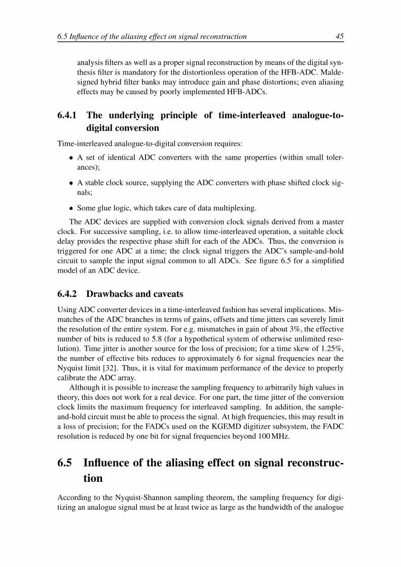
6.5 Influence of the aliasing effect on signal reconstruction 45
analysis filters as well as a proper signal reconstruction by means of the digital syn-thesis filter is mandatory for the distortionless operation of the HFB-ADC. Malde-signed hybrid filter banks may introduce gain and phase distortions; even aliasingeffects may be caused by poorly implemented HFB-ADCs.
6.4.1 The underlying principle of time-interleaved analogue-to-digital conversion
Time-interleaved analogue-to-digital conversion requires: A set of identical ADC converters with the same properties (within small toler-ances);
A stable clock source, supplying the ADC converters with phase shifted clock sig-nals;
Some glue logic, which takes care of data multiplexing.
The ADC devices are supplied with conversion clock signals derived from a masterclock. For successive sampling, i.e. to allow time-interleaved operation, a suitable clockdelay provides the respective phase shift for each of the ADCs. Thus, the conversion istriggered for one ADC at a time; the clock signal triggers the ADC’s sample-and-holdcircuit to sample the input signal common to all ADCs. See figure 6.5 for a simplifiedmodel of an ADC device.
6.4.2 Drawbacks and caveatsUsing ADC converter devices in a time-interleaved fashion has several implications. Mis-matches of the ADC branches in terms of gains, offsets and time jitters can severely limitthe resolution of the entire system. For e.g. mismatches in gain of about 3%, the effectivenumber of bits is reduced to 5.8 (for a hypothetical system of otherwise unlimited reso-lution). Time jitter is another source for the loss of precision; for a time skew of 1.25%,the number of effective bits reduces to approximately 6 for signal frequencies near theNyquist limit [32]. Thus, it is vital for maximum performance of the device to properlycalibrate the ADC array.
Although it is possible to increase the sampling frequency to arbitrarily high values intheory, this does not work for a real device. For one part, the time jitter of the conversionclock limits the maximum frequency for interleaved sampling. In addition, the sample-and-hold circuit must be able to process the signal. At high frequencies, this may result ina loss of precision; for the FADCs used on the KGEMD digitizer subsystem, the FADCresolution is reduced by one bit for signal frequencies beyond 100 MHz.
6.5 Influence of the aliasing effect on signal reconstruc-tion
According to the Nyquist-Shannon sampling theorem, the sampling frequency for digi-tizing an analogue signal must be at least twice as large as the bandwidth of the analogue

46 Properties of the KGEMD subsystem
Figure 6.5: Model of an ADC device. Each time a conversion is initiated by a clock signal, thecurrent input signal is sampled by the sample-and-hold circuit and the sampled volt-age level is retained as long as the conversion is in progress. After completion ofthe conversion process inside the ADC core, the result can be accessed at the digitaloutputs. The conversion of the analogue value is accomplished with regard to thereference voltage. The output value is calculated according to
Dout ' int ()( 2N * 1 +-,.( U / * U 0URe f 1
12+)+ , where N denotes the number of ADC out-
put bits, U / and U 0 indicate the differential ADC inputs and URe f is the referencevoltage.
signal; otherwise the reconstruction of the sampled waveform will not succeed perfectly.If this condition is not fulfilled, i.e. there are spectral contributions of the analogue signalbeyond the Nyquist frequency, these contributions are aliased down to the first Nyquistzone. Thus, frequencies beyond the Nyquist frequency are converted into frequenciesbelow the Nyquist limit.
For signals exclusively containing spectral components within one of the Nyquistzones, which are delimited by multiples of the Nyquist frequency, the aliasing effect doesnot create any problems. The reconstruction algorithm can retrieve the original waveformfrom the samples despite the aliasing. An example of a sine wave signal with a frequencybeyond the Nyquist limit is shown in figure 6.6. The aliasing effect has not been takeninto account for the reconstruction; hence, the frequency of the original sine wave is justmapped into the first Nyquist zone.
However, for signals containing spectral contributions of multiple Nyquist zones at thesame time, the signal reconstruction will fail because of the ambiguities; it is impossible toretrieve the original signal, since it is not known, whether a specific spectral component isoriginating from one or the other Nyquist zone. Figure 6.7 illustrates the effect of aliasingfor a composition of signals.
By—at least—attenuating contributions from all but one Nyquist zone, the effect ofaliasing on the signal reconstruction can be suppressed. This can e.g. be accomplishedby inserting an analogue filter (often referred to as an anti-aliasing filter) in front of the

6.6 Effective trigger level vs. PMT pulse duration 47
Figure 6.6: Aliasing effect due to sampling beyond the first Nyquist zone. The amplitude axisis subdivided into units of ADC channels. A sine wave to be digitized by the FADCdevices is shown (solid line); due to the fact, that the signal is routed through theKGEMD input circuitry, it experiences a drop in the beginning. The frequency of thatsignal (133MHz) exceeds the Nyquist frequency of the digitizer subsystem KGEMD(125MHz). After digitizing the waveform, the reconstruction of the sine wave resultsin an interpolated waveform (dashed line), which is aliased down to the first Nyquistzone, i.e. it contains frequencies below the Nyquist limit. High frequency compo-nents may therefore be mistaken as low frequency components after sampling and asubsequent waveform reconstruction.
sampling device. However, the filtering cannot be accomplished by means of digital post-processing, since the problem arises already during the sampling itself.
The KGEMD digitizer subsystem does not contain such an anti-aliasing filter; there-fore, it is possible to process frequencies beyond the Nyquist limit. On the other hand, thelack of such a filter makes the KGEMD vulnerable to the aliasing effect.
6.6 Effective trigger level vs. PMT pulse durationOne of the branches of the high gain splitting circuitry is feeding the comparator, whichdefines the trigger condition depending on the preset threshold, with the high gain sourcesignal. In order to allow a fine-grained adjustment of the threshold level, the compara-tor is not fed with the raw source signal directly; instead, an additional amplifier stageprovides the comparator with an increased signal strength. Since the reference voltage(i.e. the threshold) of the comparator is provided by a DAC device offering 12 bit volt-age resolution, the amplification is the only way to get over the limited resolution of thethreshold setting.
However, according to measurements on the KGEMD subsystem and simulations per-

48 Properties of the KGEMD subsystem
Figure 6.7: Aliasing of an interference signal, that has been added to a simulated single particlepulse. The interference signal’s frequency has been chosen to exceed the Nyquistfrequency by a few percent; the upper waveform shows the signal prior to the sam-pling, whereas the lower waveform shows the results of the signal reconstruction.Apart from real interferences, this can serve as an example of the effect of aliasingon high frequency components of a pulse signal.
formed on the SPICE model of the KGEMD subsystem’s input circuitry (see appendix C),the additional amplifier stage is highly frequency dependent, i.e. the amplification factorexhibits a drop in the high frequency range. This loss of amplification results in a triggerthreshold, which is effectively higher than the value for the low frequency range. Theeffective trigger threshold vs. the full pulse duration at half maximum (FDHM) is shownin figure 6.8.
Although it would be possible to overcome the constraints of the amplifier stage re-garding the signal fidelity by employing another type of amplifier and by differently rout-ing traces on the PCB, the data taking performance of the KGEMD would not benefitfrom these modifications. The most prominent impact of the response on the trigger sys-tem can be observed for m.i.p. pulse signals, since those signals are relatively short withregard to the FDHM. However, by adjusting the comparator threshold of the KGEMD unitaccordingly, these pulse signals will nevertheless result in trigger signals. The quality ofthe waveform sampling is not affected by the limitations of this stage anyway.

Figure 6.8: Effective trigger level vs. full duration at half maximum (FDHM). The results havebeen derived from a simulation performed on the model of the KGEMD input cir-cuitry as presented in appendix C; a stimulus of the type described in appendix A hasbeen used to evaluate the dependency. The effective trigger level with respect to thepreset threshold voltage has been plotted.

Figure 6.9: Overview diagram of the KGEMD’s internal structure [2]; the sketch has been rotatedfor enhanced visibility. The KGEMD unit is equipped with two channels, whichare simultaneously digitizing the mixed signals of the high gain and the low gainphotomultipliers, respectively. Only the channel dedicated to the high gain PMTs, isillustrated in more detail; the low gain (LG) channel is only symbolically denoted,since it is built exactly the same way as the high gain (HG) channel, apart from thecomparator and its surrounding parts. The KGEMD is receiving time stamp signalsfrom the main KASCADE time base via optical links. Another optical link, operatedat a raw data rate of 1.2 Gbit/s (corresponding to 1 Gbit/s for the payload data rate),is established for the transmission of data packets containing—among other things—time stamp information and multiplexed samples of both the high gain and the lowgain channel. The data transmission is initiated, if the comparator, which is fed withthe high gain signal, encounters a trigger condition, which requires, that the high gainphotomultiplier source signal is crossing the threshold level of the comparator.

Chapter 7
Summary and outlook
In July 2005, the installation of the new FADC-based data acquisition system in theGrande array of the KASCADE-Grande experiment has been finished. The DAQ sys-tem has been commissioned concurrently to the original Grande DAQ system, which itoutperforms in many respects.
The measures taken in order to operate the FADC-based system in parallel, have beendescribed within this thesis. Since it is only possible to reach the full potential of a highperformance data acquisition system, which is capable of supplying pulse shape infor-mation at a high resolution in addition to the energy spectra and arrival times, if detailedinformation on the system constraints as well as on the interactions of both DAQ systemsare available, these items have been examined as a part of this thesis.
Although the new FADC-based system meets most of its design goals, others requiremeans of compensation in order to achieve optimal performance data. Some of the meth-ods for compensation are already covered by this thesis, other issues may have to beworked on in future. For example, automatic intercalibration has not yet been imple-mented completely. Sophisticated methods of digital signal processing, e.g. noise sup-pression or digital filtering, have not been developed yet. These items will require addi-tional research and efforts.
However, the full pulse shape data of extensive air shower events, which trigger thecentral event builder, is recorded and kept. Thus, these means of data post-processing canbe applied to the resulting data files, once the respective algorithms have been developed.
On the other hand, the interaction of both data acquisition systems can create prob-lems. Within the scope of this thesis, the effects on the data taking by the FADC-basedsystem have been estimated. Furthermore, methods for partly compensating for theseimpacts have been developed.
The FADC-based data acquisition system will be further improved and additionalfunctionality will be implemented. The capabilities and the flexibility of the FADC-baseddata acquisition system have not yet been exploited entirely. The data taking during thenext few years will provide valuable shower data of events in the high energy range cov-ered by the Grande array.


Appendix A
Synthesis of PMT pulse stimuli
In order to conduct some of the SPICE simulations of this thesis, a stimulus had to becreated with a pulse shape similar to that of photomultiplier pulses caused by the incidenceof a single particle.
While the Landau distribution can, in general, be considered a rough estimate of thereal signal shape for simulations, it is, in most cases, not suitable for a SPICE simulation.Usually, the software engine of a SPICE simulator is not capable of evaluating arbitrarymathematical expressions in order to provide a stimulus signal. Moreover, evaluating acomplex expression is time consuming and the result of the expression has to be calculatedfor every simulation step. For a—in terms of the time resolution—fine-grained analysis,the evaluation of the stimulus expression will already consume too much time.
With the SPICE simulator used for the simulations of this thesis1, it is not possible touse arbitrary functions as a stimulus. However, it is possible to select a damped sine waveas the stimulus. By choosing the parameters accordingly, photomultiplier pulses can beemulated to some extent. The equation has the following form:
Ustim t 2 Ae23 t t0 4 λ sin 2π f t t0 5 (A.1)
Here, the amplitude can be adjusted by the A parameter, while the pulse duration and theshape of the tail are determined by f and λ . The peak position is controlled by the t0 pa-rameter. The reason for applying stimuli signals similar to the real waveforms, is, amongother things, the spectral composition, which plays an important role for classifying theresponse behaviour of devices under simulation.
Figure A.1 illustrates the dependency of the amplitude on time for a typical dampedsine wave stimulus. For comparison, a Landau distribution, approximated by the Moyalfunction [34], has been plotted as well. The function values were evaluated from thefollowing equation for appropriately chosen parameters λMoyal and AMoyal:
UMoyal t 2 AMoyal
6exp λMoyal t t0 exp λMoyal t t0
2π (A.2)
In some cases, the sharp kink at the beginning of the damped sine wave stimulus can causeproblems, since the first derivative of the stimulus exhibits a discontinuity here, resultinge.g. in high frequency contributions to the respective spectrum.
1LTSpice by Linear Technology

Figure A.1: Typical damped sine wave stimulus (solid line). The Moyal approximation of theLandau distribution is plotted for illustration (dashed line).

Appendix B
Example of a splitting device
An example of a splitting circuit has been developed as a consequence of the results fromchapter 5. A draft of the schematic diagram is shown in figure B.1.
The operational amplifier1 selected is a state-of-the-art type [22]. It offers low noise(0.95 nV/ 7 Hz) and low distortion at high speed ratings. Its input impedance is aboutfive orders of magnitude higher than that of a standard 50 Ω signal source. Thus, thissingle-stage splitter should only put a negligible amount of load to the source.
The operational amplifier employed exhibits unstable behaviour for an unity gain con-figuration; therefore, it has been configured for an amplification by a factor of two andthe voltage levels are corrected by means of serial resistors, which provide the impedancematching at the same time. Furthermore, the operational amplifier used in the schematicis sensitive to complex loads, which are attached to the output directly, e.g. a transmissionline. The serial resistors provide decoupling from the complex component of the signalsink, thereby minimizing the problem.
The frequency response of the splitting device has been evaluated for one splitterchannel using a SPICE model of the device. The -3 dB bandwidth of the device can begathered from figure B.2; it can be estimated to 568 MHz.
A splitting device should provide highly symmetric output signals to both signal sinks,i.e. the differential signal should be vanishingly small. From figure B.3, it can be verified,that this prerequisite is fulfilled.
Because of the overall properties of the device, this example of a versatile splittingdevice will suffice for many splitting tasks, where the bandwidth meets the requirements.This makes it e.g. suitable for the frequency range covered by the digitizer subsystemKGEMD.
1AD8099 by Analog Devices [33]

Figure B.1: Example of a splitting device. Input and output terminals of the device are termi-nated using 50 Ω resistors; coaxial cables matching this impedance can therefore beconnected directly. Since the operational amplifier is not stable for unity gain, it hasbeen configured for an amplification factor of two and the output voltage is dividedagain by the same factor using a serial resistor, which at the same time provides theimpedance matching for the output terminals.
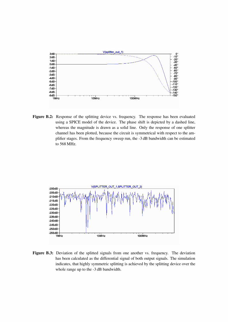
Figure B.2: Response of the splitting device vs. frequency. The response has been evaluatedusing a SPICE model of the device. The phase shift is depicted by a dashed line,whereas the magnitude is drawn as a solid line. Only the response of one splitterchannel has been plotted, because the circuit is symmetrical with respect to the am-plifier stages. From the frequency sweep run, the -3 dB bandwidth can be estimatedto 568 MHz.
Figure B.3: Deviation of the splitted signals from one another vs. frequency. The deviationhas been calculated as the differential signal of both output signals. The simulationindicates, that highly symmetric splitting is achieved by the splitting device over thewhole range up to the -3 dB bandwidth.


Appendix C
SPICE model of the KGEMD inputcircuitry
The SPICE [4] model shown in figure C.1 has been derived from the schematic diagramof the digitizer subsystem (KGEMD) [2]. All components, which do not affect the dy-namic characteristics of the KGEMD input circuitry, have been replaced by less complexelements (partly objects intrinsic to the SPICE software1) or have even been removedcompletely without substitutes, for simplicity. An example of the latter category are thepower supply bypassing components, which have been omitted, because the power supplywiring is lossless by definition in SPICE simulations, i.e. there is no need for bypassingmeasures. On the other hand, e.g. voltage references for shifting the input voltage rangeor adjusting the operation point of the amplifier stages in figure C.1 are mandatory forthe proper operation of the circuitry; however, it does not matter, exactly how the voltagereference circuit is working internally. Therefore, the voltage reference sub-circuits havebeen replaced by standard SPICE DC voltage source objects.
By reducing the number of components involved in the simulation, the number ofwiring nodes decreases. Taking into account, that the SPICE models of operational am-plifiers [29, 28], used to assemble the KGEMD input circuitry model, are rather complex,i.e. they use up a considerable amount of wiring nodes internally [29, 28], the limits ofthe respective simulation engine may be exceeded easily. Since the voltages and currentsof each single wiring node of a SPICE model must be evaluated by means of numeri-cal computing for every simulation time step throughout the complete simulation run, itis advisable to keep the number of wiring nodes as low as possible. In rare cases, thenumerical computation procedure—the Newton-Raphson iteration method is used as ofversion 3 of Berkeley SPICE—may even fail to converge for models containing too manywiring nodes. The main reason for keeping the number of wiring nodes low, is, how-ever, the duration of the simulation for a fine-grained analysis in terms of the time stepresolution.
1The LTSpice variant by Linear Technology has been used for the simulation.

60 SPICE model of the KGEMD input circuitry
C.1 Limitations of the SPICE modelAlthough the KGEMD input circuitry has been modeled to match the real device asclosely as possible, the accuracy of the simulation is limited by several factors. First,the models of the amplifier sub-circuits [29, 28] do not perform simulations of all prop-erties; for example, there is no simulation counterpart for the following properties of thereal components:
inherent noise, i.e. noise that is originating from the device itself, even though thedevice may be in a quiescent state otherwise;
distortion effects caused by non-linearities;
common-mode rejection ratio (CMRR); for an ideal differential amplifier, the out-put voltage should equal zero, in case, the differential input voltage equals zero,i.e. the input levels are equal. However, for a real device, the output voltage isslightly depending on the absolute input levels; the CMRR indicates the suppres-sion of the effect.
In addition, actually only the properties of simulated components and sub-circuits com-prising the KGEMD input circuitry as well as their interconnections are simulated usingSPICE. However, for a real setup, i.e. real hardware components, there are additionalissues, that have to be considered for optimal performance. These include:
PCB layout constraints; depending on trace routing, copper area arrangement andcomponent placement, parasitic capacities and inductivities are introduced, whichare not covered by the simulation. Moreover, real copper traces exhibit non-zeroresistance, which usually does not comply with the properties of the wiring in aSPICE simulation;
interferences caused by surrounding circuitry; in general, the circuitry to be ana-lyzed using SPICE modeling techniques, is treated as an insulated device, i.e. adevice, which is not exposed to interfering signals caused by adjacent sources. Incontrast, real hardware devices may even malfunction due to interferences;
non-ideal components; parasitic contributions result in modifications to the overallproperties, which are not modeled by basic SPICE components.
Nevertheless, despite these limitations, the SPICE model presented can provide a clueto the overall performance and properties of the KGEMD input circuitry, thereby allowingto estimate its pulse signal fidelity.
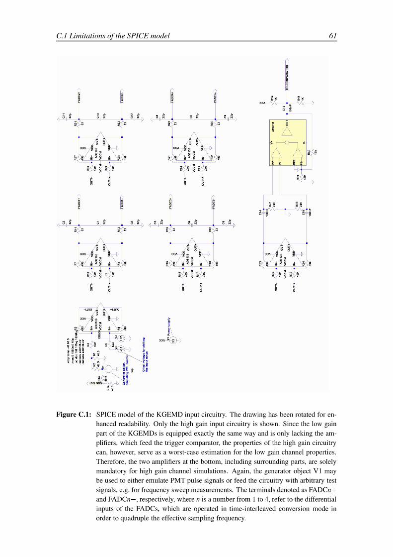
C.1 Limitations of the SPICE model 61
Figure C.1: SPICE model of the KGEMD input circuitry. The drawing has been rotated for en-hanced readability. Only the high gain input circuitry is shown. Since the low gainpart of the KGEMDs is equipped exactly the same way and is only lacking the am-plifiers, which feed the trigger comparator, the properties of the high gain circuitrycan, however, serve as a worst-case estimation for the low gain channel properties.Therefore, the two amplifiers at the bottom, including surrounding parts, are solelymandatory for high gain channel simulations. Again, the generator object V1 maybe used to either emulate PMT pulse signals or feed the circuitry with arbitrary testsignals, e.g. for frequency sweep measurements. The terminals denoted as FADCn 1and FADCn * , respectively, where n is a number from 1 to 4, refer to the differentialinputs of the FADCs, which are operated in time-interleaved conversion mode inorder to quadruple the effective sampling frequency.


Appendix D
Characteristics of the “Active Probe”
The “Active Probe” device has been developed in order to enable the digitizer subsystemof the new FADC-based DAQ system to intercept mixed PMT signals from the originalGrande DAQ system, which is operated concurrently.
The device has been designed with several goals in mind.
It should only put a marginal amount of extra load on the intercepted signal. Theinput impedance of the employed amplifier is about 105 times higher than theimpedance of the signal source. Therefore, the additional load is negligible.
There should be no extra noise originating from the intercepting device. Since theoriginal signal chain is kept and no active component is introduced in between itscomponents, there is virtually no way to introduce noise contributions into the orig-inal signal chain. However, the internal noise of the intercepting device’s activecomponent is added to the signal, that is read and processed by the digitizer com-ponent. The operational amplifier1 used to build the “Active Probe” device offers alow noise factor of 12.5 nV/ 7 Hz. This helps to minimize the effect.
In order not to reduce the digitizing accuracy of the KGEMD subsystem by intro-ducing time jitter, it is advisable to employ an operational amplifier, which featuresan active feedback stage, since the phase accuracy can be improved by means ofsuch a stage [23].
The frequency response up to (at least) the digitizer’s Nyquist frequency needs tobe flat in order to provide high pulse signal fidelity to the KGEMD input signal. Byselecting an adequate type of operational amplifier, this can be guaranteed for the“Active Probe” device. In addition, special care has been taken to design the printedcircuit board (PCB) of the device according to the manufacturer’s recommendationswith respect to trace routing and power bypassing (among other things).
The device has to be located near the output connector of the signal source andthere must not be a branch line connecting the “Active Probe” device to the originalsignal pathway to be spied on. Otherwise, reflections and interference may occur,which would cause modifications to the original pulse signals. The “Active Probe”
1Analog Devices AD8130

64 Characteristics of the “Active Probe”
Figure D.1: SPICE model of the “Active Probe” device as deployed in the Grande array ofthe KASCADE-Grande experiment for intercepting the PMT pulse signals fromthe original Grande data acquisition system. The central component of the “ActiveProbe” offers active feedback [23] and is represented by its manufacturer suppliedSPICE model [28].
device, that has been developed for deployment with the Grande station equipment,has therefore been designed to be a small card, sized only 20 50 mm2. Thus, it ispossible to attach it directly to the output connector of the signal source.
D.1 Results from a simulation of the “Active Probe”The frequency response of the device has been evaluated by conducting a frequency sweepanalysis on its SPICE model (as shown in figure D.1); that is, the amplitude and phaseshift were evaluated while the frequency has been increased gradually up to the Nyquistfrequency of the digitizer subsystem KGEMD. The response of the “Active Probe” deviceis shown in figure D.2; except for a little amplitude rise of 5% near the Nyquist frequency,the response is flat, in agreement with the design goals. The phase shift is merely causedby the propagation delay time of the active component.

D.1 Results from a simulation of the “Active Probe” 65
Figure D.2: Dynamic characteristics of the “Active Probe” device. The SPICE simulator has per-formed a frequency sweep analysis covering the frequency range up to the Nyquistfrequency of the FADC-subsystem KGEMD, i.e. up to 125 MHz. The solid line in-dicates the dependency of the amplification factor on frequency, whereas the phaseshift vs. frequency is plotted as a dashed line. According to the results, the “ActiveProbe” exhibits a maximum deviation of 5% (corresponding to $ 0 8 4 dB) from a flatfrequency response.


LIST OF FIGURES
List of Figures
1.1 Energy spectrum of primary cosmic rays in differential form . . . . . . . 31.2 Schematic views of an extensive air shower . . . . . . . . . . . . . . . . 5
2.1 Schematic layout and energy range of KASCADE-Grande . . . . . . . . 122.2 Schematic layout of KASCADE . . . . . . . . . . . . . . . . . . . . . . 132.3 Setup of the central detector of KASCADE . . . . . . . . . . . . . . . . 13
3.1 Signal amplitude degradation caused by passive mixing . . . . . . . . . . 173.2 A coarse SPICE model of the PMT pulse mixer . . . . . . . . . . . . . . 183.3 Setup for an analysis of the mixer-shaper interaction . . . . . . . . . . . . 203.4 Signal impact on the signal caused by the shaping amplifier . . . . . . . . 223.5 Spectral modifications caused by the shaping amplifier . . . . . . . . . . 233.6 Spectral projection function and quadratic fit . . . . . . . . . . . . . . . . 233.7 Digitally post-processed shaping amplifier input signal . . . . . . . . . . 24
4.1 Conceptual design of the KGEMD unit . . . . . . . . . . . . . . . . . . . 284.2 Overview of the functional units of the FADC-DAQ . . . . . . . . . . . . 29
5.1 Schematics of a simple type of current mirror . . . . . . . . . . . . . . . 355.2 Schematics of the Widlar current mirror . . . . . . . . . . . . . . . . . . 355.3 Block schematic of the active probe device . . . . . . . . . . . . . . . . . 365.4 Block schematic of a multi-stage splitting device . . . . . . . . . . . . . 365.5 Block schematic of a single-stage splitting device . . . . . . . . . . . . . 375.6 Frequency response of a two-stage splitting unit . . . . . . . . . . . . . . 38
6.1 KGEMD baseline variation vs. temperature . . . . . . . . . . . . . . . . 416.2 Frequency response of the KGEMD vs. temperature . . . . . . . . . . . . 426.3 Response of the KGEMD input circuitry excited by a square wave signal . 436.4 KGEMD response to a square wave after response compensation . . . . . 446.5 Model of an ADC device . . . . . . . . . . . . . . . . . . . . . . . . . . 466.6 Aliasing effect due to sampling beyond the first Nyquist zone . . . . . . . 476.7 Aliasing of an interference signal . . . . . . . . . . . . . . . . . . . . . . 486.8 Effective trigger level vs. FDHM . . . . . . . . . . . . . . . . . . . . . . 496.9 Overview diagram of the KGEMD’s internal structure . . . . . . . . . . . 50
A.1 Typical damped sine wave stimulus . . . . . . . . . . . . . . . . . . . . 54
B.1 Example of a splitting device . . . . . . . . . . . . . . . . . . . . . . . . 56

68 LIST OF FIGURES
B.2 Response of the splitting device vs. frequency . . . . . . . . . . . . . . . 57B.3 Deviation of the splitted signals vs. frequency . . . . . . . . . . . . . . . 57
C.1 SPICE model of the KGEMD input circuitry . . . . . . . . . . . . . . . . 61
D.1 SPICE model of the “Active Probe” device . . . . . . . . . . . . . . . . . 64D.2 Dynamic characteristics of the “Active Probe” device . . . . . . . . . . . 65

LIST OF TABLES
List of Tables
2.1 Properties of the KASCADE-Grande detector components . . . . . . . . 11
3.1 Characteristics of the photomultiplier tube . . . . . . . . . . . . . . . . . 16
4.1 Properties of the FADC-based DAQ system . . . . . . . . . . . . . . . . 32


List of Acronyms
Acronym Explanation
ADC Analogue-to-digital converterCRC Cyclic redundancy checkDAC Digital-to-analogue converterDAQ Data acquisition (system)DC Direct currentDFT Discrete Fourier transformDMA Direct memory accessEAS Extensive air showerFADC Flash analogue-to-digital converterFDHM Full duration at half maximumFFT Fast Fourier transformFIFO First in, first out (register)FPGA Field programmable gate arrayGPS Global positioning systemHFB-ADC Hybrid filter bank analogue-to-digital converterIBIS Input/output buffer information specificationKASCADE Karlsruhe shower core and array detectorKGEMD KASCADE-Grande electromagnetic detector digitizer boardKGEMP KASCADE-Grande electromagnetic detector PCI interface cardKGEMS KASCADE-Grande electromagnetic detector storage boardKGEMT KASCADE-Grande electromagnetic detector trigger receiver cardLST Limited streamer tubeLVDS Low voltage differential signalingm.i.p. Minimum ionizing particleMWPC Multi-wire proportional chamberMTD Muon tracking detectorPC Personal computerPCB Printed circuit boardPCI Peripheral component interconnectPMT Photo multiplier tubeSCSI Small computer system interface
continued on next page

72 List of Acronyms
continued from previous page
Acronym Explanation
SPICE Simulation program with integrated circuit emphasisTDC Time-to-digital converterVME Versa module eurocard

Bibliography
[1] S. Over, diploma thesis, Development and commissioning of data acquisition sys-tems for the KASCADE-Grande experiment, University of Siegen, 2004
[2] Y. Kolotaev, 2005, private communication.
[3] D. V. Camin et al., Galvanically isolated and linear transmission of analog current-signals using the optically coupled current-mirror architecture, Nuclear Instrumentsand Methods A535 (2004) 485-490
[4] L. W. Nagel, SPICE2: A Computer Program to Simulate Semiconductor Circuits,University of California, Berkeley ERL-M520 (1975)
[5] P. L. Biermann et al., Cosmic Rays from PeV to ZeV, Stellar Evolution, SupernovaPhysics and Gamma Ray Bursts, preprint astro-ph/0302201
[6] see e.g. references in: C. Grupen, Astroparticle physics, Springer-Verlag, Berlin,2005
[7] J. Zabierowski et al., Large muon tracking detector in the KASCADE EAS exper-iment, Proceedings 27th International Cosmic Ray Conference (ICRC 2001), 810-813
[8] A. Haungs et al., The KASCADE-Grande experiment, Proceedings 28th Interna-tional Cosmic Ray Conference (ICRC 2003), 985-988
[9] M. Muller et al., A measurement of the energy spectrum of unaccompanied hadrons,Proceedings 28th International Cosmic Ray Conference (ICRC 2003), 101-104
[10] A. Haungs et al., Astrophysics of the knee in the cosmic ray energy spectrum, ActaPhysica Polonica B 35 (2004) 331-339
[11] J. Candia et al., Cosmic ray spectrum and anisotropies from the knee to the secondknee, J. Cosmol. Astropart. Phys. 05, 3 (2003)
[12] M. Nagano and A. A. Watson, Ultrahigh-energy cosmic rays, Reviews of ModernPhysics 72 (2000) 689-728
[13] S. Eidelman et al., Review of Particle Physics, Physics Letters B 592, 1 (2004)
[14] O. Alkhofer, Introduction to cosmic radiation, Verlag Carl Thiemig Munchen, 1975.
[15] T. J. Kutter, The water cherenkov detector in the Auger experiment, FZKA-6396

[16] T. Antoni et al. The cosmic ray experiment KASCADE, Nuclear Instruments andMethods A513 (2003) 490-510
[17] M. Aglietta, The cosmic ray primary composition in the ’knee’ region through theEAS electromagnetic and muon measurements at EAS-TOP, Astroparticle Physics21 (2004), 583-596
[18] M. Aglietta, UHE cosmic ray event reconstruction by the electromagnetic detectorof EAS-TOP, Nuclear Instruments and Methods A336 (1993), 310-321
[19] S. Over, 2005, private communication.
[20] D. Zimmermann, 2005, private communication.
[21] B. Schofer, 2004, private communication.
[22] R. Seibert, 2005, private communication.
[23] J. Wong, Active feedback improves amplifier phase accuracy, Analog Devices Ap-plication Notes AN-107 (1987)
[24] V. Andrei, diploma thesis, Reconstruction algorithms for the FADC DAQ system ofthe KASCADE-Grande experiment, University of Siegen, 2004
[25] M. Frigo and S. Johnson, The design and implementation of FFTW3, Proceedingsof the IEEE 93 (2005) 216-231
[26] J. Pickerd, DSP in high performance oscilloscopes, Tektronix Inc., 2005
[27] Product specification XP3462, Photonis, 1999
[28] Differential receiver amplifiers AD8129/AD8130, data sheet and SPICE model,Analog Devices, Rev. A
[29] Low distortion differential ADC driver AD8138, data sheet and SPICE model, Ana-log Devices, Rev. E
[30] J. Bird, Detection of a cosmic ray with measured energy well beyond the expectedspectral cutoff due to cosmic microwave radiation, preprint astro-ph/9410067
[31] S. Velazquez, T. Nguyen and S. Broadstone, Design of hybrid filter banks for ana-log/digital conversion, IEEE Trans. Signal Processing 46 (1998) 956-967
[32] A. Montijo, Accuracy in interleaved ADC systems, Hewlett-Packard Journal, 1993.
[33] Ultralow distortion, high speed 0.95 nV/ 7 Hz voltage noise Op Amp, Analog De-vices, Rev. B
[34] J. Moyal, Theory of ionization fluctuations, Phil. Mag. 46 (1955)

Acknowledgement
My gratitude goes out to all those, who made this thesis possible.In the first place, this is without doubt Prof. Dr. Peter Buchholz, who made it possible
for me to work on the interesting KASCADE-Grande experiment. Furthermore, I wouldlike to thank him for the opportunity to take part in the research within the scope ofanother exciting experiment in the future.
I am also very grateful that Prof. Dr. Claus Grupen agreed to revise this thesis—despitethe brevity of the time available.
I can hardly thank all the people of our working group adequately for the pleasantatmosphere. It made working on the experiment and the thesis a lot easier. Very specialthanks to my colleagues who worked on the KASCADE-Grande experiment as well, sincethey were all able and willing to work as a team.
Also, I am indebted to Marc Bruggemann, Sven Over and Dirk Zimmermann, notonly for patiently proofreading the contents of my thesis but also for sharing my sense ofhumour, irony and even sarcasm. This led to a lot of funny discussions e.g. during lunch.
Thanks to Dr. Wolfgang Walkowiak for the hints on—among other things—formalaspects of my thesis.
In addition, I would like to thank Yury Kolotaev and Bernd Schofer for their designwork regarding the KASCADE-Grande experiment and I’d like to extend my thanks to themembers of the mechanical and the electronics workshops, who contributed to buildingthe setup of the experiment.
I would like to express my gratitude to all my friends in Ludenscheid and Dortmund,some of them I know really well for many years, some even for decades. I hope we willstay in contact.
And finally, I am very grateful for the support my family gave to me. Especially myparents have given support to me all of my life, in every respect. Thanks to you!


Erklarung
Hiermit versichere ich, dass ich diese Arbeit selbststandig verfasst habe und keineanderen als die angegebenen Quellen und Hilfsmittel benutzt habe.
Thomas Backer