Chapter 01- Practical Data Acquisition for instrumentation and control system
Upload
khangminh22Category
view
0download
0
pnODUCT "~
PUBLICATIONS
For Sale Through IBM Branch Offices
We are pleased to send you this ~omplimentary copy o~.a newly '!rmted publication. Addltl0!1al. copies are available from the DistributIOn Center, Mechanicsburg.
G. W. Goesch, Manager Department G24
Author: J. A. Wilson
Field Engineering
Maintenance Manual
Data Acquisition and Control System
SY26-5956-6
For Sale Through IBM Branch Offices
Field Engineering
Maintenance Manual
TI@@@ Data Acquisition and Control System
SY26-5956-6
Preface
This manual contains maintenance information for the following units of the IBM Data Acquisition and Control System:
IBM 1801 and 1802 Processor-Controllers IBM 1803 Core Storage Unit IBM 1826 Data Adapter Unit IBM 1828 Enclosure IBM 1851 Multiplexer Terminal IBM 1856 Analog Output Terminal
The data processing input/output units used in the 1800 system are provided with separate maintenance manuals that
*Manuals referred to in this publication that have an Order No. with a four character prefix are identical in content to the same manual without the initial prefix character. (e.g. SY26-xxxx is the same in content as Y26-xxxx.)
Seventh Edition (February, 1970)
contain information required to service those units. Other manuals that are used in servicing the 1800 system are listed in the IBM Field Engineering Bibliography, 1800 Data Acquisition and Control System (Order No. SY26-0560).*
It is assumed that the user of this manual is familiar with 1800 system programming techniques and that he understands the functional and operational aspects of all system areas. Hexadecimal numbers, if not otherwise identified, are preceded by a "slash" (e.g., /3000) to distinguish them from decimal numbers.
Service Aids included in this manual are 24,25,35,44, 65,66,69, 129, 134, and 172.
This manual (Order No. SY26-5956-6) is a complete revision of, and makes obsolcte, Order No. SY26-5956-5. Changes to the text, and small changes to illustrations, are indicated by a vertical line to the left of the change; changed or added illustrations are denoted by the symbol. to the left of the caption.
Significant changes or additions to the specifications contained in this publication are continually being made. When using this publication in connection with the operation of IBM equipment, check the latest FE publications Systems Sequence Listing, Order No. SY20-0073, for revisions or contact the local IBM Branch Office.
The illustrations in this manual have a code number in the lower corner. This is a publishing control number and is not related to the subject matter.
Copies of this and other IBM publications can be obtained through IBM Branch Offices.
A form for reader's comments is provided at the back of this publication. If the form has been removed, send your comments to the address below.
This manual was prepared by the IBM Systems Development Division, Product Publications, Department G24, San Jose, California 95114.
ii (2/70)
Safety.. . . . . . . . . . . . . . . . . . . . . . . . . . . . . . . . . . . . . . . . . .. vi
Abbreviations ..................................... viii
CHAPTER 1. REFERENCE DATA AND DIAGNOSTIC TECHNIQUES ........................ 1-1
Section 1. Reference Data . . . . . . . . . . . . . . . . . . . . . . . . . .. 1-1
1.1 LOGIC DIAGRAMS ..................... 1-28
1.1.1 ALD Logic Block Symbology. . . . . . . . . . . . . . 1-28
1.1.2 FEALD Logic Block Symbology. . . . . . . . . . . . 1-28
1.1.3 Machine Frame and Gate Designations ....... 1-28
1.1.4 Logic Page Identification. . . . . . . . . . . . . . . . . . 1-29
1.1.5 System Paperwork Binder . . . . . . . . . . . . . . . . . 1-30
1.2
1.2.1
1.2.2
1.2.3
1.2.4
1.2.5
1.2.6
MANUALL Y CONTROLLED WIRING CHANGES ............................ 1-30
Authorization for Wiring Changes .......... 1-32
Data Channel Assignment. . . . . . . . . . . . . . . . . 1-32
Timer Interval Reassignment. . . . . . . . . . . . . . . 1-33
Interrupt Assignments ................... 1-33
System/360 Adapter Address Reassignment. . . 1-34
Communications Adapter and Line Adapter .............................. . 1-34
1.2.7 Editing Diagnostic Programs . . . . . . . . . . . . . . . 1-35
Section 2. Diagnostic Techniques ..................... 1-35
1.3 ON-LINE SERVICING LIMITATIONS. . . . . . . 1-35
1.3.1 Use of Auxiliary Storage. . . . . . . . . . . . . . . . . . 1-35
1.3.2 Power Removal and Component Plugging. . . . . 1-35
1.3.3 Channel Termination. . . . . . . . . . . . . . . . . . . . . 1-36
1.3.4 System/360 Adapter. . . . . . . . . . . . . . . . . . . . . 1-36
1.4 MARGINAL CHECKING. . . . . . . . . . . . . . . .. 1-36
1.5 SLT MAINTENANCE. . . . . . . . . . . . . . . . . . . . 1-37
1.5.1 SLTContactWear ....................... 1-37
1.5.2 Wire Color Codes ....................... 1-37
1.5.3 Machine Cable Installation ................ 1-37
1.6 CRITICAL CIRCUITS AND LEVELS ....... 1-38
1.6.1 Sample Pulse Drivers (SPD's) .............. 1-38
1.6.2 Singleshots (SS) ........................ 1-38
1.6.3 Phase A/B ............................. 1-38
1.7
1.7.1
1.7.2
1.7.3
Contents
<>"
CORE STORAGE.. . ... ... .... .... ...... 1-40
Collection of Error Data . . . . . . . . . . . . . . . . . . 1-40
Main Storage Addressing and Selection ...... 1-41
Core Storage Display Procedure ............ 1-42
1. 7.4 Scoping Techniques ..................... 1-43
1.7.5 Swapping BSM Address Assignments ........ 1-44
1.7.6 Array Swapping (Physical) ................ 1-44
1.7.7 Trouble Diagnosis ...................... 1-44
1.7.8 Core Storage Waveforms . . . . . . . . . . . . . . . . . . 1-53
1.7.9 Current Measurement .................... 1-53
1.8 PROCESS INPUT/OUTPUT. . . . . . . . . . . . . . . 1-53
1.8.1 Analog Input .......................... 1-53
1.8.2 Analog Input Waveforms ................. 1-55
1.8.3 Multiplexer Troubleshooting Techniques ..... 1-57
1.8.4 1851 Service Voltages ................... 1-60
1.8.5 Programming Rules and Restrictions ........ 1-60
1.8.6 Analog Inpu t Repeatability ............... 1-61
1.8.7 Analog Ou tpu t 1-62
1.9 DATA PROCESSING INPUT/OUTPUT...... 1-62
1.9.1 DP I/O Trouble Diagnostic ................ 1-62
1.9.2 1442 Card Read Punch ., . . . . . . . . . . . . . . . . . 1-62
CHAPTER 2. CONSOLE AND MAINTENANCE FEATURES .......................... 2-1
2.1 PROGRAMMER'S CONSOLE ............. 2-1
2.1.1 Switches and Message Lamps .............. 2-1
2.1.2 Toggle Switches 2-4
2.1.3 Indicator Lamps 2-4
2.1.4 Register Display Lamps and Switches ....... 2-6
2.2 INITIAL PROGRAM LOAD (IPL) .......... 2-6
2.2.1
2.2.2
2.2.3
2.3
2.4
1442 Standard IPL Procedure
1054 Standard IPL Procedure
IPL into Any Core Location
ERROR CIlECK CIRCUITS
2-6
2-7
2-7
2-7
MAINTENANCE DIAGNOSTIC PROGRAMS .......................... 2-8
1800 FEMM (2/70) iii
2.4.1
2.4.2
2.4.3
2.5
2.5.1
2.5.2
Program Tests . . . . . . . . . . . . . . . . . . . . . . . . . . 2-8
Documentation . . . . . . • . . . . . . . . . . . . . . . . . . 2-9
Diagnostic Approach . . . . . . . . . . • . . . . . . . . . . 2-9
I/O MONITOR INTERFACE PANELS....... 2-9
Interface Connectors ..................•. 2-9
Functions of Switches - 1801/1802 Interface Panel ......................... 2-10
2.6 AUXILIARY STORAGE ................. 2-11
2.7 CE INTERRUPT ......... "............ 2-11
2.8 CE MODE. . . . . . . . . . . . . . . . . . . . . • . . . . . . . 2-11
2.9 PROGRAMMABLE TEST LATCH ......... 2-12
2.10 CE CYCLE-STEAL TEST, . . . . . . .. . . . . . . . . 2-12
2.11 GENERAL TEST EQUIPMENT............ 2-13
2.11.1 I/O Monitor Units ...................... 2-13
2.11.2 Oscilloscope. . . . . . . . . . . . • . . . . . . . . . . . . . . 2-13
2.11.3 CE Indicator Latch Card .............•... 2-13
2.11.4 ExtenderCard ......................... 2-14
2.11.5 Seven-Position Binary Counter ............ 2-14
2.11.6 Remote Switch Box ..................... 2-15
2.12 PROCESS I/O rEST EQUIPMENT ......... 2-16
2.12.1 Fluke DC Differential Voltmeter 2-16
2.12.2 Analog Input Calibration Facility 2-17
2.12.3 Digital Input Test Card. . . . .. . . . . . . . . . . . . . 2-18
2.12.4 Digital Output Test Cable ................. 2-18
2.12.5 1856 DAC/PVR Extender ................ 2-19
2.13 CORE STORAGE TEST EQUIPMENT....... 2-19
2.13.1 Oscilloscope. . . . . . . . . . . . . . . . . . . . . . . . . . . 2-19
2.13.2 Differential Scope Cable ......... . . . . . . . . . 2-19
2.13.3 Current Probe ....... . . . . . . . . . . . . . . . . . . . 2-19
2.13.4 Core Storage Current Probing Card 2-19
2.13.5 Card Offset and Four-Inch Jumpers 2-20
2.13.6 Thermometer. . . . . . . . . . . . . . . . . . . . . . . . . . 2-20
2.13.7 Meter. . . . . . . . . . . . . . . . . . . . . . . . . . . . . . . . 2-20
CHAPTER 3. PREVENTIVE MAINTENANCE .......... . 3-1
CHAPTER 4. CHECKS, ADJUSTMENTS, AND REMOVALS ......................... . 4-1
Section 1. Basic Unit ............................. . 4-1
4.1 PANEL LAMPS. . . . . . . . . . . . . . . . . . . . . . . . . 4-1
iv (2/70)
4.1.1
4.1.2
4.2
4.2.1
4.2.2
4.3
Indicator Lamp Removal/Replacement ...... 4-1
Message Lamp Removal/Replacement ....... 4-1
GATE BLOWERS.. . .. .. .. .. .. .. .. .. . .. . 4-1
Blower Removal/Replacement ............. 4-1
Filter Replacement ...................... 4-1
CENTRAL PROCESSING UNIT ........... 4-1
4.3.1 Service Check. . . .. . . . . . . . . . . . . . . . . . . . . . 4-1
4.3.2 Phase A/B Adjustment ................... 4-1
4.3.3 Operations Monitor. . . . . . . . . . . . . . . . . . . . . . 4-2
4.4 CORE STORAGE .. . . . . . . . . . . . . . . . . . . . . . 4-3
4.4.1 General Precautions ...................•. 4-3
4.4.2 Service Check .......................... 4-3
4.4.3 Core Storage Adjustments. . . . . . . . . . . . . . . . . 4-3
4.4.4
4.4.5
4.4.6
4.5
4.5.1
4.5.2
Array Removal/Replacement .............. 4-3
Core Storage Board (BSM) Removal/ Replacement . . . . . . . . . . . . . . . . . . . . . . . . . . . 4-3
Core Storage Diodes Removal/Replacement. . . 4-4
CHANNEL CONTROL . . . . . . . . . . . . . . . . . . . 4-4
Service Check - Interval Timers .. . . . . . . . • . . 4-4
Service Check - Interrupt ................ 4-4
Section 2. Features .............................. . 4-4
4-4 4.6
4.6.1
4.6.2
4.7
4.7.1
4.7.2
4.7.3
4.8
4.8.1
4.8.2
4.8.3
4.9
4.9.1
4.10
4.10.1
4.10.2
4.11
1816-1053 ADAPTER .................. .
Service Check .......................... 4-4
Singleshot Adjustments .................. 4-4
1054-1055 ADAPTER. . . . . . . . . . . . . . . . • . . . 4-4
Service Check .......................... 4-4
Singleshot Adjustments .................. 4-4
Oscillator Adjustment . . . . . . . . . . . . . . . . . . . . 4-5
1442 ADAPTER . . . . . . . . . . . . . . . . . . . . . . . . 4-5
Service Check ......................... .
Singleshot Adjustments ................. .
4-5
4-5
Read Emitter Strobe Timing . . . . . . . . . . . . . . . 4-5
1443 ADAPTER ....................... 4-5
Service Check ......................... .
1627 ADAPTER ....................... .
Service Check
Plotter Speed
4-5
4-5
4-5
4-5
1810 DISK STORAGE. . . . . . . . . . . . . . . . . . . 4-5
4.12 MAGNETIC TAPE CONTROL. . . . . . . . . . . .. 4-5
4.12.1 Service Check - Tape Control Unit ......... 4-5
4.12.2 Oscillator Timing ....................... 4-5
4.12.3 Service Check - Read Clock Timing. . . . . . . . . 4-5
4.12.4 Service Check - Write Clock Timing. . . . . . . . . 4-6
4.12.5 Service Check - Delay Counter Timing. . . . . . . 4-6
4.12.6 Service Check - Signal Acceptance and Rejection Levels ........................ 4-7
4.12.7 Singleshot Adjustment ................... 4-7
4.12.8 Final Amplifier Read/Write Adjustment ..... 4-7
4.13 SYSTEM/360 ADAPTER ................. 4-11
4.13.1 Service Check .......................... 4·11
4.13.2 SingleshotAdjustments................... 4-11
4.14 ANALOG INPUT........................ 4-11
4.14.1 Precautions. .. . . . . . . . . . . . . . . . . . . . . . . . . . 4-11
4.14.2 Service Checks ......................... 4-12
4.14.3 Analog Input Calibration. . . . . . . . . . . . . . . . . . 4-12
4.14.4 Singleshot Adjustments. . . . . . . . . . . . . . . . . . . 4-12
4.14.5 Resistance Bulb Thermometer. . . . . . . . . . . . . . 4-12
4.15 ANALOG OUTPUT ..................... 4-12
4.15.1 Service Check. . . . . . . . . . . . . . . . . . . . . . . . . . . 4-12
4.15.2 Analog Output Calibration ................ 4-12
4.15.3 1856 Blower Removal/Replacement. . . . . . . . . 4-12
4.15.4 1856 Blower Filter Replacement. . . . . . . . . . .. 4-13
4.16 DIGITAL INPUT. . . . . . . . . . . . . . . . . . . . . . . . 4-14
4.16.1 Service Check - Digital Input and Process Interrupt. . . . . . . . . . . . . . . . . . . . . . . . . . . . . . 4·14
4.16.2 Service Check - Pulse Counter. . . . . . . . . . . . . 4-14
4.17 DIGITAL OUTPUT...................... 4·14
4.17.1 Service Check ..... ',' . . . . . . . . . . . . . . . . . . . . 4-14
4.17.2 SingJeshot Adjustments. . . . . . . . . . . . . . . . . . . 4-14
4.18 SELECTOR CHANNEL. . . . . . . . . . . . . . . . . . . 4-14
4.18.1 Service Check .......................... 4-14
4.18.2 Singleshot Adjustments. . . . . . . . . . . . . . . . . . . 4-14
4.19 COMMUNICATIONS ADAPTER...... ...... 4-14
4.19.1 Service Check 4-14
4.19.2 Adjustments. . . . . . . . . . . . . . . . . . . . . . . . . . . 4-14
CHAPTER 5. POWER SUPPLIES ..................... 5-1
Section 1. Basic Unit. . . . . . . . . . . . . . . . . . . . . . . . . . . . . . . 5-1
5.1
5.2
5.3
5.4
5.4.1
5.4.2
PRECAUTIONS. . . . . . . . . .. . . . . . . . . . . . . . . 5-1
SYSTEM POWER·ON PROCEDURE......... 5-1
SYSTEM POWER·OFF PROCEDURE........ 5-1
ADJUSTMENT AND REMOVAL PROCEDURES . . . . . . . . . . . . . . . . . . . . . . . . . 5-1
MPS Power Supply Adjustment. . . . . . . . . . . . . 5-1
MPS Power Supply Removal/ Replacement . . . . . . . . . . . . . . . . . . . . . . . . . . . 5-2
5.4.3 Power Supply Filter Replacement. . . . . . . . . . . 5·2
5.5 TROUBLESHOOTING PROCEDURES ...... 5·3
5.5.1 Power Supply Overload .................. 5-3
Section 2. Features ................................ 5·3
5.6
5.6.1
5.7
POWER PAC - 1856 ANALOG OUTPUT TERMINAL. . . . . . . . . . . . . . . . . . . . . . . . . . . . 5-3
Power Pac Voltage Adjustment. . . . . . . . . . . . . 5-3
PRECISION VOLTAGE REFERENCE....... 5-3
CHAPTER 6. LOCATIONS. ......................... 6-1
6.1 LOCATIONS SHOWN IN SYSTEM DIAGRAMS ........................... 6-1
6.1.1 System. . . . . . . . . . . . . . . . . . . . . . . . . . . . . . . 6-1
6.1.2 1801 and 1802 Processor-Controller. . . . . . . . . 6·1
6.1.3 1826 Data Adapter Unit .................. 6·1
6.1.4 1828 Enclosure. . . . . . .. . .. . .. . . . . . . . . . . . 6-1
6.2 FRAME NUMBERING SySTEM..... ...... 6-1
6.3 BOARD LOCATIONS.................. .. 6·1
6.4
6.4.1
6.4.2
6.5
6.5.1
6.5.2
6.5.3
6.5.4
6.5.5
6.6
WIRED LOGIC (WL) JUMPERING ......... 6-3
Interrupt, Cycle Steal, IPL . . . . . . . . . . . . . . . . . 6-3
Other. . . . . . . . . . . . . . . . . . . . . . . . . . . . . . . . . 6-3
COMPONENT LOCATIONS INDEX......... 6-3
1801 and 1802 Processor·Controller . . . . . . . . . 6-3
1803 Core Storage Unit. . . . . . . . . . . . . . . . . . . 6·3
1826 Data Adapter Unit, Models 1 and 2. . . . . . 6-3
1826-3 Data Adapter Unit. . . . . . . . . . . . . . . . . 6-4
1828 Enclosure. . . . . . . . . . . . . . . . . . . . . . . . . 6-4
LOCATIONS FIGURE LISTING .......... . 6-4
APPENDiXES.... .... .................... ...... . .. A-l
1800 FEMM (2/70) v
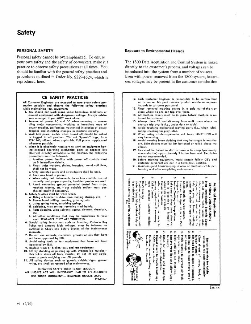
Safety
PERSONAL SAFETY
Personal safety cannot be overemphasized. To ensure your own safety and the safety of co-workers, make it a practice to observe safety precautions at all times. You should be familiar with the general safety practices and procedures outlined in Order No. S229-1624, which is reproduced here.
CE SAFETY PRACTICES All Customer Engineers ore expected to take every safety precaution possible and observe the following safety practices while maintaining IBM equipment:
1. You should not work alone under hazardous conditions or around equipment with dangerous voltage. Always advise your manager if you MUST work alone.
2. Remove all power AC and DC when removing or assembling major components, working in immediate area of power supplies, performing mechanical inspection of power supplies and installing changes in machine circuitry.
3. Wall box power switch when turned off should be locked or tagged in off position. "Do not Operate" tags, form 229-1266, affixed when applicable. Pull power supply cord whenever possible.
4. When it is absolutely necessary to work on equipment hav· ing exposed operating mechanical parts or exposed live electrical circuitry anywhere in the machine, the following precautions must be followed: a. Another person familiar with power off controls must
be in immediate vicinity. b. Rings, wrist watches, chains, bracelets, metal cuff links,
shall not be worn, c, Only insulated pliers and screwdrivers shall be used. d. Keep one hand in pocket. e. When using test instruments be certain controls are set
correctly and proper capacity, insulated probes are used, f. Avoid contacting ground potential (metal Aoor strips,
machine frames, etc, - use suitable rubber mats pur· chased locally if necessary).
5. Safety Glasses must be worn when: c. Using a hammer to drive pins, riveting, staking, etc. b. Power hand drilling, reaming, grinding, etc. c. Using spring hooks, attaching springs. d. Soldering, wire cutting, removing steel bands. e. Parts cleaning, using solvents, sprays, cleaners, chemicals,
etc. f. All other conditions that may be hazardous to your
eyes. REMEMBER, THEY ARE YOUR EYES. 6, Special safety instructions such as handling Cathode Roy
Tubes and extreme high voltages, must be followed as outlined in CEM's and Safety Section of the Maintenance Manuals,
7. Do not use solvents, chemicals, greases or oils that have not been approved by IBM:
B. Avoid using tools or test equipment that have not been approved by IBM,
9. Replace worn or broken tools and test equipment. 10. lift by standing or pushing up with stronger leg muscles
this takes strain off back muscles. Do not lift any equip· ment or parts weighing over 60 pounds.
11, All safety devices such ds guards, shields, signs, ground wires, etc. shall be restored after maintenance.
KNOWING SAFETY RULES IS NOT ENOUGH AN UNSAFE ACT WILL INEVITABLY LEAD TO AN ACCIDENT
USE GOOD JUDGMENT - ELIMINATE UNSAFE ACTS 229-1264·1
vi (2/70)
Exposure to Environmental Hazards
The 1800 Data Acquisition and Control System is linked directly to the customer's process, and voltages can be introduced into the system from a number of sources. Even with power removed from the 1800 system, hazardous voltages may be present in the customer termination
12, Each Customer Engineer is responsible to be certain that no action on his part renders product unsafe or exposes hazards to customer personnel.
13, Place removed machine covers in a safe out.of·the-way place where no one can trip over them.
14. All machine covers must be in place before machine is reo turned to customer.
15. Always place CE tool kit away from walk areas where no one can trip over it (i.e., under desk or table).
16. Avoid touching mechanical moving parts (Le" when lubri· cating, checking for play, etc,).
17. When using stroboscope - do not touch ANYTHING - it may be moving,
18. Avoid wearing loose clothing that may be caught in machinery, Shirt sleeves must be left buttoned or rolled above the elbow.
19, Ties must be tucked in shirt or have a tie clasp (preferably nonconductive) approximately 3 inches from end, Tie chains are not recommended.
20. Before starting equipment, make certain fellow CE's and customer personnel are not in a hazardous position.
21, Maintain good housekeeping in area of machines while per· forming and after completing maintenance,
5';!~ Ul c ' <>3 ' ~CT
"tl -0 0 ~~
~Q. )
~ .
, :il33 :;:00 -·c c: 0 __
~ :T:T

area. All customer lines are potentially dangerous and should be regarded as live circuits.
When entering any part of the customer's process area, observe all safety precautions and regulations. Check the following items with customer safety personnel:
1. The need for safety glasses, hard hats, or special clothing.
2. Particular route that must be taken to and from installation. Escort required?
3. Smoking restrictions. 4. Restrictions on use of electrical or other spark-
producing tools. 5. Exposure to high voltages. 6. Exposure to heavy machinery or other equipment. 7. Exposure to splashing acids, molten metal, hot
liquids, etc. 8. Exposure to toxic gases and vapors. 9. Warning alarms and emergency exits.
When servicing IBM units that are installed in customer consoles or racks, pay particular attention to nearby units or devices that can present a safety hazard.
Machine Warning Labels
Heed the warning labels placed in hazardous areas of the machines. They are placed there for your protection.
Power Supplies
Before working on any power supply, remove power from the unit and allow at least one minute for capacitors to discharge. Although all power supplies are provided with bleeder resistors to drain off capacitor charges when power is dropped, it is wise to check the dc output with a meter before attempting maintenance.
Power Cords
Check power cords periodically for safe condition and proper ground connections.
Line-Powered Equipment
Oscilloscopes and other line-powered equipment must always be grounded through the third-wire grounding conductor in the power cord.
EQUIPMENT PRECAUTIONS
Customer Interface
The 1800 system is an integral part of the customer's operation. Do not, under any circumstances, work on any part
of the system without the knowledge and consent of the customer.
Be especially careful not to impulse a digital or analog output point that is connected to a process device.
Core Storage
Use extreme caution when working around core storage. Do not leave the core storage unit unattended when covers are removed.
Solid-State Components
Avoid operating the system for prolonged periods with the SLT card covers removed.
Care must be exercised when grounding signal lines, in order to prevent applying a voltage instead of a ground, or grounding the output of an emitter-follower circuit. Electrical overloads, for periods of even a few microseconds, can seriously damage or destroy transistors.
Because of the danger of shorting between adjacent cards, it is not advisable to remove or replace SLT cards with power on.
The following types of cards must never be removed with power on:
Drivers and amplifiers Core storage cards Power supply cards Multiplexer cards
Relay Multiplexer Cards
Use care when removing and inserting multiplexer cards. Fingerprints, pencil marks, and other contaminants decrease the leakage resistance of these cards. Do not use cleaning solvents or card contact lubricants, and do not permit the protective coating on the card to become damaged.
Before a relay card is inserted in the card gate, it should be held upright and tapped lightly to clean the contacts of any excess mercury. Sharp blows should be avoided; do not tap the card against a hard surface or drive the card into its socket with a blow from the hand. Improper handling of relay cards can make the relay inoperable or cause it to operate outside specified limits.
If common-mode voltage in excess of 10 volts (ac or dc) is present on the customer input lines, or if there is a possibility of the occurrence of such voltage, the lines must be disconnected by the customer prior to removal or insertion of the multiplexer relay card in that channel. Mercury bridging of the relay points during removal or insertion of the card may impress the entire common-mode voltage across the flying capacitor, relay points, or amplifier, resulting in component damage.
1800 FEMM (2/70) vii
Abbreviations
A-reg accumulator register EA effective address ADA analog driver amplifier EBCDIC extended binary-coded-decimal interchange ADC analog-to-digital converter code AI analog input EC engineering change ALD automated logic diagram ECA engineering change announcement AMAR analog multiplexer address register ECAD error check analysis diagram AD analog output ECO electronic "contact" operate ASCII American standard code for information ENQ enquiry
interchange EOC end of conversion AWG American wire gauge EDT end of table aux auxiliary EDT end of transmission
EPO emergency power off B-reg storage buffer register ETB end of transmission block BCC block check character ETX end of text bfr buffer BO branch out BS block switch F-reg format register BSC binary synchronous communications FC feature code BSM basic storage module FEALD Field Engineering automated logic diagram
FESRR Field Engineering Systems Reference Report CA communications adapter FET field-effect transistor CAB channel address buffer FF flip-flop CAF customer assignment form FL flip-latch CAR channel address register CC chain command hex hexadecimal CCW channel command word HLSE high-level, single-ended CD chain data HSDA high-speed data acquisition CEM Customer Engineers Memorandum Hz hertz (cycles per second) CMRR common-mode rejection ratio CPU central processing unit I-reg instruction register CRC-16 cyclic redundancy check (16 bits) I/A indirect addressing CRP Card Read Punch (IBM 1442) ICAR instrument calibration and repair CS cycle steal ILSW interrupt level status word CSA cycle steal acknowledge I/O input/output CSU core storage unit 10CC input/output control command CSW channel status word IPL initial program load
ITB intermediate transmission block D-reg arithmetic factor register DAC digital-to-analog converter LA line adapter DAD digital and analog output LRC longitudinal redundancy check DAU Data Adapter Unit (IBM 1826) LSB least significant bit DC data channel DCU data control unit M-reg storage address register DDC direct digital control MAR-2 Manufacturing Assembly Report DET double-emitter transistor #2 (field use) DI digi tal in pu t MDM maintenance diagram manual DIMAL disk maintenance library MES miscellaneous equipment specification DLE data link escape MI multi-input DO digital output MLC machine level control DP data processing MLR machine location report DPC direct program control Mod-reg modify register DSW device status word MPS medium power sta!1dard
viii (2/70)
MPX multiplex(er), R-relay, S-solid-state SLD simplified logic diagram
MPX Multiprogramming Executive (a program- SLI suppress length indicator
ming system) SLT solid logic technology SMS standard modular system
NAK negative acknowledgment SOH start of heading SPD sample pulse driver
Op-reg operation code register SRL Systems Reference Library SS singleshot (multivibrator)
P parity SSC single storage cycle
PC pulse counter STX start of text
P-C processor-controller SYN synchronous idle
PCI program control interruption PI process interrupt T-reg tag register
PID program identification tag selector channel control line
PISW process interrupt status word TIC transfer in channel
PO pulse output TSX Time-Sharing Executive (a programming
POC process operator's console system)
PVR precision voltage reference TTD temporary text delay
Q-reg accumulator extension register V-reg temporary accumulator register UDCD unit data and control diagram
RBT resistance bulb thermometer VJT unijunction transistor
RO register output RPQ request for price quotation VRef reference voltage (core storage)
VRC vertical redundancy check VSA sense amplifier voltage (core storage)
SAR storage address register S&H sample-and-hold (amplifier) WC word counter SC shift counter SCR silicon-controlled rectifier XIO execute input/output SCRID SCR indicator driver XR index register SI single instruction SIO start input/output / precedes hexadecimal numbers (base 16)
IHOO FEMM (2/70) ix
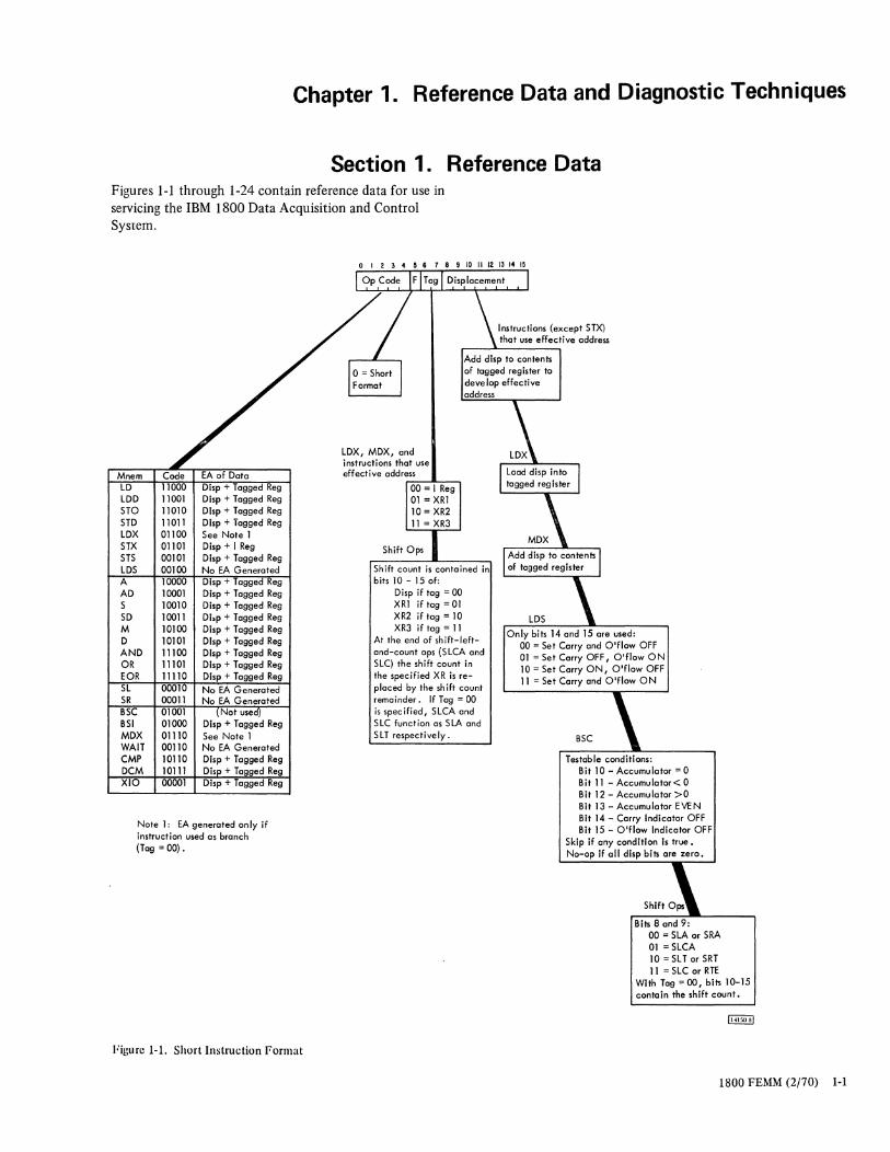
Chapter 1. Reference Data and Diagnostic Techniques
Section 1. Reference Data Figures 1-1 through 1-24 contain reference data for use in servicing the IBM 1800 Data Acquisition and Control System.
Mnem LD LDD STO STD LDX STX STS LDS A AD S SD M D AND OR EOR SL SR BSC BSI MDX WAIT CMP DCM XIO
Code 11000 11001 11010 11011 01100 01101 00101 00100 10000 10001 10010 10011 10100 10101 11100 11101 11110 0001 00011 01001 01000 01110 00110 10110 10111 00001
Dlsp + Tagged Reg Dlsp + Tagged Reg Dlsp + Tagged Reg Dlsp + Tagged Reg See Note 1 Disp + I Reg Dlsp + Tagged Reg No EA Generated Disp + Tagged Reg Dlsp + Tagged Reg Disp + Tagged Reg Dhp + Tagged Reg Disp + Tagged Reg Dlsp + Tagged Reg Dlsp + Tagged Reg Dlsp + Tagged Reg Dlsp + Tagged Reg
No EA Generated No EA Generated
Not used Dlsp + Tagged Reg See Note 1 No EA Generated Dlsp + Tagged Reg Dis + Tagged Reg Dlsp + Tagged Reg
Note I: EA generated only if instruction used as branch (Tag = 00).
Figure 1·1. Short Instruction Format
Instructions (except STX) that use effective address
Add dlsp to contents of lagged register to develop effective
LDX, MDX, and instructions that use effect i ve address
Shift Ops
Disp if tag = 00 XRl if tag = 01 XR2 if tag = 10 XR3 if tag = 11
address
At the end of shift-Ieftand-count ops (SLCA and SLC) the shift count in the specified XR is replaced by the sh ift count remainder. If Tag = 00 is specified, SLCA and SLC function as SLA and S LT respectively.
LDS
Only bits 14 and 15 are used: 00 = Set Carry and O'flow OFF 01 = Set Carry OFF, O'flow ON 10 = Set Carry ON, O'flow OFF 11 = Set Carry and O'flow ON
BSC
Testable conditions: Bit 10 - Accumulator = 0 Bit 11 - Accumulator< 0 Bit 12 - Accumulator >0 Bit 13 - Accumulator EVEN Bit 14 - Carry Indicator OFF Bit 15 - O'flow Indicator OFF
Skip if any condition Is true. No-op If all disp bits are zero.
Bits 8 and 9: 00 = SLA or SRA 01 = SLCA 10 = SL T or SRT 11 = SLC or RTE
With Tag = 00, bits 10-15 contain the shift count.
IBOO FEMM (2/70) 1-1
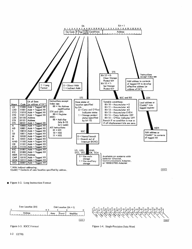
EA of Data Mnem Code (or address of EA *) LD 11000 Addr + Tagged XR LDD 11001 Addr + Tagged XR STO 11010 Addr + Tagged XR STD 11011 Addr + Tagged XR LDX 01100 Address STX 01101 Address STS 00101 Addr + To ed XR A 10000 Addr + Tagged XR AD 10001 Addr + Tagged XR S 10010 Addr + Tagged XR
EA EA+ 1 o I 2 3 4 & 6 7 6 9 10 II 12 13 14 15 0 I 2 3 4 5 6 7 6 9 10 II 12 13 14 15
I ?p, C,od~ IF IT~glll~1 Sonldi:i~s I I I I I I ' ~d,dr7ss, , , I I I ' I
STS
Instructions except Store status at Index ops: location specified
00 = No Address by EA: modification o = Carry and O'flaw
STX and LDX: Indicator status 00 = I Register 1 = Storage protec t
MDX: status (specified 00 = Add dlsp by bit 15)
(bits 8-15) to C (addr)
All Instructions: 01 =XRl BSC 10 =XR2
STS Instructions except index cps
C lear Storage Protect bit
Bit 15 = 1: Add address to contents
Set Storage Protect bit
of tagged XR to develop effective address (or address of EA *)
BSC and BSI LDX
Testable conditions: Load address or Bit 10 - Accumulator = 0 C{addr) * inta Bit 11 - Accumulator <0 tagged register Bit 12 - Accumulator >0 Bit 13 - Accumulator EVEN Bit 14 - Carry Indicator OFF Bit 15 - O'flow Indicator OFF
Branch if no condition Is true or if all displacement bits are zero.
MDX
Add address or SD 10011 Addr + Tagged XR C(addr) * ta contents M 10100 Addr + Tagged XR 11 =XR3 0= Normal branch
D 10101 Addr + Tagged XR 1 = Branch out of of tagged XR
AND 11100 Addr + Tagged XR Interrupt (BOSe) OR 11101 Addr + Tagged XR EOR 11110 Addr + Tagged XR BSC 01001 d r + Tagged LD, LDD, AND, BSI 01000 Addr + Tagged XR STO, STD, OR, EOR MDX 01110 Address
0= Use main } A •• ".". 0. "M'm. wI," CMP 10110 Addr + Tagged XR storage Selector Channel,
DCM 10111 Addr + To ed XR 1 = Use auxiliary Communications Adapter, XIO 00001 Addr + Tagged X R storage or 1800/2790 Adapter
* With indirect addressing. 114151Cl C(addr) = Contents of core location specified by address .
• Figure 1-2. Long Instruction Format
Even Location (EA) Odd Location (EA + 1) 15 0 4 B 15
I ' Address , I ! 1 , , ,
Figure 1-3. loee Format Figure 1-4. Single-Precision Data Word
1-2 (2/70)
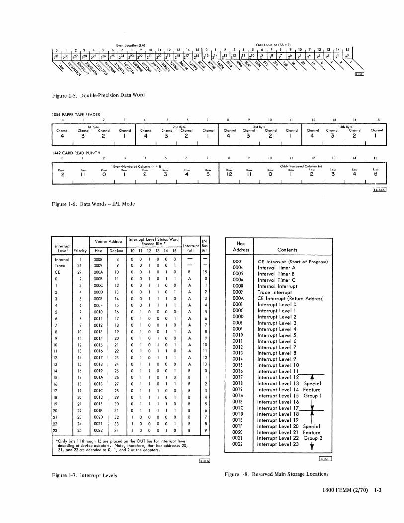
Figure 1-5. Double-Precision Data Word
1054 PAPER TAPE READER 10 II 12 13 14 15
1st Byte 2nd Byte Channel Channel Chonnel Channel Channel Channel Channel Channel Channel
3rd Byte Channel Channel Channel Channel
4th Byte Channel Channel Chermel
4 3 2 I 4 3 2 I 4 3 2 I 4 3 2 I
I I I I I I I I I I I I
1442 <;:ARD READ PUNCH 10 II 12 13 14 15
Row
12 Row
II
, Even-Numbered Columns (n + I) Row Row Row Row
o 2 3
Odd-Numbered Columns (n) 'J Row Row Row Row Row Row Row Row Row
4 5 12 II 0 I 2 3 4 5 I I I I I I I I I I I I I I
114154A1
Figure 1-6. Data Words -IPL Mode
Vector Address Interrupt Level Status Word IN interrupt
Encode Bits * Interrupt Bus Level Priority Hex Decimal 10 II 12 13 14 15 Poll Bit
Hex Address Contents
Internal I 0008 8 0 0 I 0 0 0 - -Trace 26 0009 9 0 0 I 0 0 I - - 0001 CE Interrupt (Start of Program)
0004 Interva I Timer A CE 27 OOOA 10 0 0 I 0 I 0 B 15 0005 Interva I Timer 8 0 2 OOOB II 0 0 I 0 I I A 0 0006 Interva I Timer C I 3 OOOC 12 0 0 I I 0 0 A I 0008 Interna I Interrupt 2 4 0000 13 0 0 I I 0 I A 2 0009 Trace Interrupt 3 5 OOOE 14 0 0 I I I 0 A 3 OOOA CE Interrupt (Return Address) 4 6 OOOF 15 0 0 I I I I A 4 0000 Interrupt Level 0
5 7 0010 16 0 I 0 0 0 0 A 5 OOOC Interrupt Leve I I
6 8 0011 17 0 I 0 0 0 I A 6 0000 Interrupt Level 2
7 9 0012 18 0 I 0 0 I 0 A 7
8 10 0013 19 0 I 0 0 I I A B
9 II 0014 20 0 I 0 I 0 0 A 9
10 12 0015 21 0 I 0 I 0 I A 10
II 13 0016 22 0 I 0 I I 0 A II
12 14 0017 23 0 I 0 I I I A 12
OOOE Interrupt Level 3 OOOF Interrupt Leve I 4 0010 Interrupt Leve I 5 0011 Interrupt Leve I 6 0012 Interrupt Level 7 0013 Interrupt Leve I 8 0014 Interrupt Leve I 9
13 15 0018 24 0 I I 0 0 0 A 13 0015 Interrupt Leve I 10 14 16 0019 25 0 I I 0 0 I B 0
15 17 oolA 26 0 I I 0 I 0 B I
16 18 oolB 27 0 I I 0 I I B 2
0016 Interrupt Level II 0017 Interrupt Leve I 12 OJ 0018 Interrupt Level 13 Special
17 19 OOIC 28 0 I I I 0 0 B 3 0019 Interrupt Level 14 Feature
18 20 0010 29 0 I 1 I 0 1 B 4
19 21 oolE 30 0 I 1 I I 0 B 5
20 22 oolF 31 0 1 1 -I 1 1 B 6
21 23 0020 32 I 0 0 0 0 0 B 7
22 24 0021 33 I 0 0 0 0 1 B 8
23 25 0022 34 I 0 0 0 I 0 B 9
OOIA Interrupt Leve I 15 Graup I 0018 '"te~p' L ... , '6+ OOIC Interrupt Level 17 0010 Interrupt Level 18 OOIE Interrupt Level 19 OOIF Interrupt Level 20 Special 0020 Interrupt Level 21 Feature
'Only bits 11 through 15 are placed on the OUT bus for interrupt level decoding at device adapters. Note, therefore, that hex addresses 20, 21, and 22 are decoded as 0, I, and 2 at the adapters.
0021 Interrupt Level 22 Group 2 0022 Interrupt Leve I 23 t
Figure 1-7. Interrupt Levels Figure 1-8. Reserved Main Storage Locations
1800 JlEMM (2/70) 1-3
- '!l J,. cr.;' c= ...
~ '" ~ --.J ;0 S t:l '" n §.
E: ~ x '" D-
'" n §. E-n 0
~ '" ... ~. 0 ::3 >-l ., CT Q -;:;; ~ 0 ..., ,!j
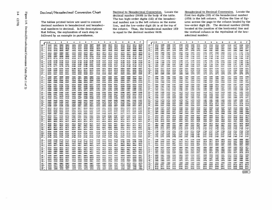
Decimal/Hexadecimal Conversion Chart
The tables printed below are used to convert decimal numbers to hexadecimal and hexadecimal numbers to decimal. In the descriptions that follow, the explanation of each step is followed by an example in parentheses.
oo!r~ I 2 3 4 5 6 7 8 9
0001 0002 0003 0004 0005 0006 0007 0008 0009 01- 0016 D017 D018 0019 D020 0021 D022 0023 D024 0025 02 _ D032 0033 0034 0035 D036 D037 0038 D039 D040 D041 03 _ D048 0049 0050 D051 D052 D053 0054 DOSS D056 D057 04_ 0064 0065 0066 0067 0068 0069 0070 0071 D072 D073 05 _ 0080 0081 0082 0083 0084 DOSS 0086 0087 0088 D089 06_ 0096 0097 0098 0099 0100 0101 0102 0103 0104 0105 07 _ 0112 0113 0114 0115 0116 0117 0118 OIl9 0120 0121 08 _ 0128 0129 0130 0131 0132 0133 0134 0135 0136 0137 09_ 0144 0145 0146 0147 0148 0149 0150 0151 0152 0153 OA_ 0160 0161 0182 0163 0164 0165 0166 0167 0168 0169 OB_ 0176 0177 0178 0179 0180 0181 0182 0183 0184 0185 OC_ 0192 0193 0194 0195 0196 0197 0198 0199 0200 0201 00_ 020S 0209 0210 0211 0212 0213 0214 0215 0216 0217 OE_ 0224 0225 0226 0227 0228 0229 0230 0231 0232 0233 OF _ 0240 0241 0242 0243 0244 0245 0246 0247 0248 0249
10_ 0256 0257 0258 0259 0260 0261 0262 0283 0264 0265 11_ 0272 0273 0274 0275 0276 0277 0278 0279 0280 0281 12 _ 0288 0289 0290 0291 0292 0293 0294 0295 0296 0297 13 _ 0304 0305 0306 0307 0308 0309 0310 0311 ('1312 0313 14 _ 0320 0321 0322 0323 0324 0325 0326 0327 0328 0329 15 _ 0338 0337 0338 0339 0340 0341 0342 0343 0344 0345 16_ 0352 0353 0354 0355 0~56 0357 0358 0359 0360 0361 17 _ 0368 0369 0370 0371 0372 0373 0374 0375 0376 0377 18 _ 0384 0385 0388 0367 0368 0369 0390 0391 0392 0393 19 _ 0400 0401 0402 0403 0404 0405 0406 0407 0408 0409 1A_ 0416 0417 0418 0419 0420 0421 0422 0423 0424 0425 1B_ 0432 0433 04~ 0435 04~ 0437 04~ 0439 0440 0441 1C_ 0448 0449 0450 0451 0452 0453 0454 0455 0456 0457 10_ 0484 0465 0486 0467 0468 0469 0470 0471 0472 0473 lE_ 0480 0481 0482 0483 0484 0485 0486 0487 0488 0489 IF _ 0496 0497 0498 0499 0500 0501 0502 6503 OS04 6505 20_ OS12 0513 0514 0515 0516 0511 0518 051Q 11'520 11521 21- 0528 0529 0530 0531 ()532 0')3'3 0')34 0535 0,),'36 0537 22 _ 0544 0545 0546 0547 0.54H 054Q 0550 0551 (1')'52 11'5'5.'3 23 _ 0560 0561 0562 0563 0564 0565 0566 0567 0.56H 11569 24 _ 0576 0577 0578 0579 05/iO 0581 (l5H2 0583 (158.1 0585 25_ 0592 0593 0594 0595 0,<)6 0')97 OSQ8 OS99 0600 06111 26 _ 0608 0609 0610 0611 0612 0613 0614 0615 0616 0617 27 _ 0624 0625 0626 0627 0628 062Q 0630 0631 0632 0633 28 _ 0640 0641 0642 0643 0644 0645 0646 0647 0646 0649 29 _ 0656 0657 0658 0659 !1Ilf,o 0661 0662 0663 0664 0665 2A_ 0672 0673 0674 0675 0676 0677 0678 0679 orlHO 0661 2B_ 0688 0689 0690 0691 0692 0693 0694 0695 0696 0697 2C_ 0704 0705 0706 0707 0708 0709 (7)0 0711 0712 0713 20_ 0720 0721 0722 0723 0724 on') 0726 0727 0728 0729 2E_ 0736 0737 0736 0739 0740 0741 0742 0743 0744 0745 2F _ 0752 0753 0754 0755 0756 0757 0758 0759 0/60 0761
30_ 0768 0769 0770 0771 0772 0773 0774 0775 0776 0777 31 _ 0784 0785 0786 0787 0788 078c) 07'lO 0791 0792 0793 32 _ OBOO 0601 0802 0603 0804 ORO') 0806 0807 IlSOR ORO<) 33_ 0816 0817 0818 0819 0820 OR21 0822 0823 0824 082.')
~- 0832 0833 0834 0835 0836 0837 0838 0839 0840 0841 35_ 0848 0849 0850 0851 0852 0853 085.1 OR5.5 08')6 0857 ~- 0864 0865 0866 0867 0868 086<) OR70 0871 OHn 0873 37 _ 0680 0881 0882 0883 0684 0885 0886 0887 0888 088C) 36_ 0896 0897 0898 0899 0900 0901 0902 0903 1l'lO4 0')0, 39 _ 0912 0913 0914 0915 0916 0917 0918 0919 Oc)20 0<J21 3A_ 0928 0929 0930 0931 0932 0933 0934 0935 W)36 0937 3B_ 0944 0945 0946 0947 0948 0949 0950 0951 0'>52 0953 3C_ 0960 0961 0962 0983 0964 0965 0966 0967 0'l68 0OOC) 30_ 0976 0977 0978 0979 0980 0981 0982 0983 OC)8-1 098'5 3E_ 0992 0993 0994 0995 0996 0997 0998 099'l 100U 1001 3F _ 1008 1009 1010 1011 1012 1013 1014 1015 1016 1017
A
0010 0026 D042 0058
0074 0090 0106 0122 0138 0154 0170 0186 0202 0218 0234 0250
0266 0282 0298 0314 0330 0346 0362 0378 0394 0410 0426 0442 0458 0474 0490 0506 0512 0538 0'5'54 0570 0586 0602 061S 0634 06,0 0666 0682 0698 0714 0730 0746 0762
0778 0794 0810 0826 0842 0858 0874 0890 o<106 092:! 0938 0954 0970 0911A 1002 1018
Decimal to Hexadecimal Conversion. Locate the decimal number (0489) in the body of the table. The two high-order digits (IE) of the hexadecimal number are in the left column on the same line, and the low-order digit (9) is at the top of the column. Thus, the hexadecimal number IE9 is equal to the decimal number 0489.
B C 0 E F
0011 0012 0013 0014 0015 40~:24 1 2 3
1025 1026 1027 0027 D028 D029 D030 D031 41_ 1040 1041 1042 1043 D043 0044 0045 0046 0047 42_ 1056 1057 1058 1059 0059 D060 0061 0062 0063 43_ 1072 1073 1074 1075
D075 0076 0077 0078 D079 44_ 1088 1089 1090 1091 0091 0092 0093 0094 D095 45 _ 1104 lI05 lI06 1107 0101 010B 0109 0110 0111 46 _ 1120 1121 lI22 lI23 0123 0124 0125 0126 0127 47 _ 1I36 1137 1138 1139 0139 0140 0141 0142 0143 48 _ 1152 lI53 lI54 lI55 0155 0156 0157 0158 0159 49 _ 1168 lI69 1170 lI71 0171 0172 0173 0174 0175 4A_ lI84 lI85 1186 lI87 0187 0188 0189 0190 0191 4B_ 1Z00 1201 1202 1203 0203 0204 0205 0206 0207 4C_ 1216 1217 1218 1219 0219 0220 0221 0222 0223 40_ 1232 1233 1234 1235 0235 0236 0237 0238 0239 4E_ 1248 1249 1250 1251 0251 0252 0253 0254 0255 4F _ 1264 1265 1266 1267
0267 0268 0269 0270 0271 50 _ 1280 1281 1282 1283 0283 0284 0285 0286 0287 51 _ 1296 1297 1298 1299 0299 0300 0301 0302 0303 52 _ 1312 1313 1314 1315 0315 0316 0317 0318 0319 53_ 1328 1329 1330 1331
0331 0332 0333 0334 0335 54 _ 1344 1345 1346 1347 0347 0348 0349 0350 0351 55 _ 1360 1361 1~2 1363 0363 0364 0365 03fl6 0367 0379 0380 0361 0382 0383
56 _ 1376 1377 1378 1379 57 _ 1392 1393 1394 1395
0395 0396 0397 0398 0399 58 - 1408 1409 1410 1411 0411 0412 0413 0414 0415 59 _ 1424 1425 1426 1427 0427 0428 0429 0430 0431 5A_ 1440 1441 1442 1443 0443 0444 0445 0446 0447 5B_ 1456 1457 1458 1459
0459 0460 0461 0462 0463 5C_ 1472 1473 1474 1475 0475 0476 0477 0478 0479 50_ 1488 1489 1490 1491 0491 0492 0493 0494 0495 5E_ 1504 1505 1506 1507 0507 0508 0509 0510 6511 5F_ 1520 1521 1522 1523 (1523 0524 0'52') 0526 0527 60_ 1536 1537 1538 1539 0')39 O'WI 0')41 0542 0543 61 _ 1552 1553 15.54 1555 115'5'5 11'5'56 OS'57 0558 OS.'59 62 _ 1568 1569 1570 1571 0571 0.572 0573 0574 0575 63 _ 1584 1585 1586 1587
0587 0588 0.589 0.'590 0591 64 _ 1600 1601 1602 1803 0603 0604 0605 0606 0607 65 _ 1616 1617 1618 1619 061Q 0620 0621 0622 0623 66_ 1632 1633 1634 16~
0635 0636 0637 H63H 063t) 67 _ 1648 1649 1650 1651
0651 06.52 0651 0654 0655 68 _ 1664 1665 1666 1667 0667 n668 0669 0670 0671 69 _ 1680 1681 1682 1683 0683 UGH4 06H.'5 0666 0687 6A_ 1696 1697 1698 1699 0699 0700 0701 0702 0703 6B _ 1712 1713 1714 1715
071'5 0716 0i17 0718 0719 6C_ 1728 1729 1730 1731 0731 (1732 0733 0/34 0735 60_ 1744 1745 1746 1747 0747 0748 0749 0750 0751 6E_ 1760 1761 1762 1763 0763 076.1 0765 0766 0767 6F _ 1776 1777 1778 1779
0779 07RO 0781 0782 0783 70 _ 1792 1793 1794 1795 0795 0796 0797 0798 0799 71 _ 1808 1809 1810 1811 0811 0812 ORI3 ORI4 0815 72 _ 1824 1825 1826 1827 0827 0828 0829 0830 0831 73 _ 1840 1841 1842 1843
0843 0844 OR45 0846 0847 74 _ 18.56 1857 1858 1859 0859 0860 0861 OR62 0863 75 _ 1872 1873 lR74 1875 0875 OR7G OH77 OR7B OB7C) 76 _ 1888 1889 1890 1891 0891 08c):! OR93 0894 0895 77_ 1'lO4 1905 1906 1907
0'lO7 0'lO8 (l<){l!) Oc)IO 0911 0923 0924 092') 0926 0927
78 _ 1920 1921 1922 1923 79 _ 1936 1937 1938 1939
0939 0')40 0941 0942 0943 7A_ 1952 1953 1954 1955 0955 0956 0957 0958 0959 7B_ 1968 1969 1970 1971
0971 0<)72 0973 0974 0975 7C_ 1984 1985 1986 1987 0987 OC)/iR 0989 0990 0991 70_ 2000 2001 2002 2003 1003 1004 1005 1006 1007 7E_ 2016 2017 2018 2019 1019 1020 1021 1022 1023 7F _ 2032 2033 2034 2035
4
1028 1044 1060 1076
1092 1108 1124 1140 lI56 1172 lI88 1204 1220 1236 1252 1268
1284 1300 1316 1332 1348 1364 1380 1396 1412 1428 1444 1460 1476 1492 1508 1524 1540 1556 1572 1588 1604 1620 1636 1652 1668 1684 1700 1716 1732 1748 1764 1780
1796 1812 1828 1844 1860 1876 1892 1908 1924 1940 1956 1972 1988 2004 2020 2036
Hexadecimal to Decimal Conversion. Locate the first two digits (IE) of the hexadecimal number (IE9) in the left column. Follow the line of figures across the page to the column headed by the low-order digit (9). The decimal number (0489) located at the junction of the horizontal line and the vertical column is the equivalent of the hexadecimal number.
5 6 7 8 9 A B C 0 E F
1029 1030 1031 1032 to33 1034 1035 1036 1037 1038 1039 10-15 1048 1047 10-18 I04C) 1050 1051 1052 1053 1054 1055 1061 1062 1063 10fl1 106, 1066 1067 1068 1069 1070 1071 1077 1078 1079 11180 1081 1082 1083 1084 108') 1086 1087 10c)3 1094 1095 1096 1097 1098 1099 lion IlOI 1102 1103 1109 1110 1111 1112 1113 111-1 IllS lII6 1117 1118 lI19 1125 1126 1127 1128 1129 1130 1131 1132 1133 1134 1135 1I41 1142 1I43 1144 II45 lI46 II47 lI48 1149 1I50 1151 lI57 1158 1159 1160 1I61 1162 lI63 116.1 lI65 lI66 1167 lI73 II74 1175 1176 1177 1I78 1179 1180 1I81 1182 lI83 1189 lI90 1191 1192 lI93 1194 lI95 1196 1197 lI98 lI99 1205 1206 1207 1208 1209 12'10 1211 1212 1213 1214 1215 1221 1222 1223 1224 1225 1226 1227 1228 1229 1230 1231 1237 1238 1239 1240 12-11 1242 1243 1244 1245 1246 1247 1253 1254 1255 1256 1257 1258 1259 1260 1261 1262 1283 1269 1270 1271 1272 1273 1274 1275 1276 1277 1278 1279
1285 1286 1287 1288 1289 1290 1291 1292 1293 1294 1295 1301 1302 1303 1304 1305 1306 1307 1308 1309 1310 1311 1317 1318 1319 1320 1321 1322 1323 1324 132') 1326 1327 1333 133-1 1335 1336 1337 1338 1339 1340 1341 1342 1343
1349 1350 1351 1352 1353 1354 1355 1356 1357 1358 1359 1365 1366 1367 1368 1369 1370 1371 1372 1373 1374 1375 1381 1382 1383 1384 1385 1386 1387 1388 1389 1390 1391 1397 1398 1399 1400 1401 1402 1403 1404 1405 1406 1407
1413 1414 1415 1416 1417 1418 1419 1420 1421 1422 1423 1429 1430 1431 1432 1433 1434 1435 1436 1437 1438 1439 1445 1446 1447 1448 1449 1450 1451 1452 1453 1454 1455 1461 1462 1463 1464 1465 1466 1467 1468 1469 1470 1471
1477 1478 1479 1480 1481 1482 1483 1484 1485 1466 1487 1493 1494 1495 1496 . 1497 1498 1499 1500 1501 1502 1503 1509 1510 1511 1512 1513 1514 1515 1516 1517 1518 1519 1525 1526 1527 1528 ' 1529 1530 1531 1532 1533 1534 1535
1541 1542 1543 1544 1545 1546 1547 1548 1549 1550 1551 1557 1558 1559 1560 1561 1562 1563 1564 1565 1566 1567 1573 1574 1575 1576 1577 1578 1579 1580 1581 1582 1583 1589 1590 1591 1592 1593 1594 1595 1596 1597 1598 1599 1805 1606 1607 1608 1609 1610 1611 1612 1613 1614 1615 1621 1622 1623 1624 1625 16Z6 1627 1628 1629 1630 1631 1837 1638 1639 16-10 1641 1642 1643 1644 1645 1646 1647 1653 1654 1855 1656 1657 1658 1659 1680 1661 1662 1663 1669 1670 1671 1672 1673 1674 1675 1676 1677 1678 1679 1685 1686 1687 1688 1689 1690 1691 1692 1693 1694 1695 1701 1702 1703 1704 170S 1706 1707 1708 1709 1710 1711 1717 1718 1719 1720 1721 1722 1723 1724 1725 1726 1727
17~ 1734 1735 1736 1737 1738 1739 1740 1741 1742 1743 1749 1750 1751 1752 1753 1754 1755 1756 1757 1758 1759 1765 1766 1767 1768 1769 1770 1771 1772 1773 1774 1775 1781 1782 1783 1784 1785 178B 1787 1788 1789 1790 1791
17C)7 1798 1799 1800 1801 1802 1803 1804 1805 1806 1807 1813 1814 1815 1816 1817 1818 1819 1820 1821 1822 1823 1829 1830 1831 1832 1833 1834 1835 1836 1837 1838 1839 1845 1846 1847 1848 1849 1850 1851 1852 1853 1854 1855
1861 1862 1863 1864 1865 1866 1887 1868 lR69 1870 1871 1877 1878 IB79 1880 1881 1882 1883 1884 1885 1886 1887 1893 1894 1895 18C)6 1897 1898 1899 1900 1901 1902 1903 19O'l 1910 1911 1912 1913 1914 1915 1916 1917 1918 1919
1925 lC)26 1927 1928 lq29 1930 1931 1932 1933 1934 1935 1941 1942 1943 1944 1c)45 1946 1947 1948 1949 1950 1951 1957 1958 1959 1960 1961 1962 1963 1964 1965 1966 1967 1973 1974 1975 lq76 1977 1978 1979 1980 1981 1982 1983
1989 1990 1991 1992 1993 1994 1995 1996 1997 1998 1999 2005 2006 2007 2008 2009 2010 .zon 2012 2013 2014 2015 2021 2022 2023 202.1 2025 2026 2027 2028 2029 2030 2031 2037 2038 2039 2040 2041 2042 2043 2044 2045 2046 2047
-oc o o
8O~:4B 81_ 20&l 82_ 2080 83_ 2096
8'- 2112 8.5 _ 2128 86_ 2144 87 _ 2160 88 _ 2116 89 _ 21c)2 8A_ 2208 HB_ 2224
8C_ 2240 80_ 22.56 8E_ 2272 8F_ 2288
90_ 2304 91_ 2320 92_ 2336 93 _ 2352 94 _ 2368 05 _ 2364 00_ 2400 97 _ 2416 98 _ 2432 00 _ 2448 OA_ 2464 9B_ 2480 OC_ 2496 9D_ 2512 OE_ 2528 9F _ 2544
AO_ 2')60 AI- 2576 A2 _ 2'592 A3_ 2808 A4 _ 2624 A5_ 26~0 A6_ 26')6 A7 _ 2672 A8 _ 2688 A9 _ 2704 AL 2720 AD- 2736 AC_ 27'52 AD_ 2768 AE_ 2784 AF_ 2Roo
BO _ 2RI6 BI _ 28']2 B2 _ 2848 B3 _ 2R6~ B4 _ 2880 B5 _ 2N<>R 86 _ 2C)12 87 _ 2428 88 _ 2944 89 _ 2960 BA_ 2976 BB_ .2992 BC_ 30Clll BD_ 3024 BE_ 3040 BF_ 3056
Dec Bin
0 0000 1 0001 2 0010 3 0011 4 0100 5 0101 6 0110 7 0111
1 2 3 4 5
2049 2050 2051 2052 2053 2065 2066 2067 2.068 2069 2081 2082 2083 2,J184 2085 2091 2098 2099 2100 2iOi
2113 2114 2115 2116 2117 2129 2130 2131 2132 2133 2145 21-16 2147 2148 2149 2161 2162 2163 2164 2165 2177 2178 2179 2180 2IBI 2193 2194 2195 2196 2197 220<) 2210 2211 2212 2213 2225 2226 2227 2228 2229
2241 2242 2243 22H 224.5 2257 2258 2259 22.60 2261 2273 2274 2275 2276 2277 2289 2290 2291 2292 2293
2305 2306 2307 2308 2309 2321 2322 2323 2324 2325 2337 2338 2339 2340 2341 2353 2354 2355 2356 2357
2369 2370 2371 2372 2373 2385 2386 2387 2388 2389 2401 2402 2403 2404 N05 2417 2418 2419 2\20 2421
2433 2434 2435 2436 2437 2449 2450 2451 2452 2453 2465 2466 2467 2468 2469 2481 2482 2483 2484 248,5
2497 2498 2499 2500 2501 2513 2514 2515 2516 2517 2529 2530 2531 2532 2533 2545 2546 2547 2548 2549 2.')61 Z5S2 2563 2'>64 2'565 2571 2.578 2579 2'580 2'581 2.'593 2594 2,595 2596 2')97 2609 2610 2611 2612 2613 2625 2626 2627 2628 2629 2641 2642 2643 26H 2645 26'57 2658 2659 2660 2661 2673 2674 2675 2676 2677 2689 2690 2691 2692 2693 2705 2706 2707 2708 2709 2721 2722 2723 2724 272'5 2737 2738 2739 2740 2741 27.'53 2754 27.55 27.'56 27'57 2769 2770 2771 2772 2773 278') 2786 2787 2788 27H9 2801 2802 2803 2804 2805
2817 2818 2819 2820 2R21 28.']3 2834 2835 2816 2N37 2R49 28S0 2851 28'52 2853 2865 2866 2867 2868. 2869 2881 2882 288') 288~ 2N85 2897 2898 2899 2900 2901 2913 2914 291.'5 2,C)16 2917 2929 29']0 2931 2932 2933 2945 2\;146 2947 294B 2949 2%1 2962 2963 2<>R-\ 2')6'5 2C)77 2978 2979 2980 29Ml 2993 2994 2995 29C)6 2997 3009 3010 3011 1012 3013 3025 3026 3027 302B 3029 3041 3042 3043 3044 ']04,5 3057 3058 3059 3060 3061
Hex Dec Bin Hex
0 8 1000 8 1 9 1001 9 2 10 1010 A 3 11 1011 B 4 12 1100 C 5 13 1101 D 6 14 1110 E 7 15 1111 F
6 7 8 9 A B C D E F
2054 2055 20")6 2057 2058 2059 2060 2061 2062 2063 2070 2071 20.2 2073 2074 2015 2076 2077 2078 2079 2086 2087 2088 2089 2090 2091 2092 2093 2094 2095 2102 2103 2104 2105 2106 2107 2108 2109 2110 2111 2118 2119 212.0 2121 2122 2123 2124 2125 2126 2127 2134 2135 \ 2136 2137 2138 2139 2140 2141 2142 2143 2150 2151 2152 21.53 2154 2155 2156 2157 21158 2159 2166 2167 2168 2169 2170 2171 2172 2173 2174 2175 2182 2183 21B4 2185 2186 2187 218B 2189 2190 2191 2198 2199 2200 2201 2202 2203 2204 2205 2206 2207 2214 2215 2216 2217 2218 2219 2220 2221 2222 2223 2230 2231 2232 2233 2234 2235 2236 2237 2238 2239 2246 2247 22~8 22~9 2250 2251 22,52 2253 2254 2255 2262 2263 2264 2265 2266 2267 2268 2269 2270 2271 2278 2279 2280 2281 2282 2283 2284 2285 2286 2287 229~ 2295 2296 2297 2298 2299 2300 2301 2302 2303
2310 2311 2312 2313 2314 2315 2316 2317 23}8 2319 2326 2327 2']28 2329 2330 2331 2332 2333 2334 2335 2342 2343 2344 2345 2346 2347 2348 2349 2350 2351 2358 2359 2360 2361 2362 2363 2364 2365 2366 2367 2374 2375 2376 2377 2378 2379 2380 2381 2382 2383 2390 2391 2392 2393 2394 2395 2396 2397 2398 2399 2406 2407 2408 2409 2410 2411 2412 2413 2414 2415 2422 2423 2424 2425 2426 2427 2428 2429 2430 2431
2438 2439 2440 2441 2442 2443 2444 2445 2446 2447 2454 24,55 2456 2457 2458 2459 2480 2461 2462 2463 2470 2471 2472 2473 2474 2475 2476 2477 2478 2479 2486 2487 2-188 2489 2490 2491 2492 2493 2494 2495 2502 2503 2504 2505 2506 2507 2508 2509 2510 2511 2518 2519 2520 2521 2522 2523 2524 2525 2526 2527 2534 2535 2536 2537 2538 2539 2540 2541 2542 2543 2550 2551 2552 2553 2554 2555 2556 2557 2558 2559 2566 2.567 2')68 2.569 2'570 2571 2')72 2'573 2574 2'575 2~82 2583 2'584 258'5 2586 2587 2'5N8 2'5R9 2590 2591 2598 2599 2600 2601 2602 2603 26(J~ 2605 2606 2607 2614 2615 2616 2617 2618 2619 2620 2621 2622 2623 2630 2631 2632 26.']3 2634 2635 2636 2637 2638 2639 2646 2647 264H 264<J 2650 2651 26'52 2M3 26'54 265'5 2662 2663 266' 266'5 2666 2667 2668 2669 2670 2671 2678 2679 26HO 2681 2682 2683 2684 26B5 2686 2687 2694 26C)5 2f)t)6 2697 269B 2699 2700 2701 2702 2703 2710 2711 2712 2713 2714 2715 2716 2717 2718 2719 2726 2727 2728 2729 2730 2731 2732 2733 2734 2735 2742 2743 2744 2745 2746 2747 2748 2749 27'50 2751
27'58 27.'59 2760 2761 2762 2763 2764 276'5 2766 2767 2774 277'5 2776 2777 2778 2779 27RO 2781 27R2 2783 2790 27ql 27lJ2 2793 271,14 279.'5 2796 271)7 2798 2799 2806 2807 2808 2ROC) 2810 2811 2812 2813 2814 2815
2822 2823 2824 2R2:5 2826 2827 2R2R 2829 2830 2831 2R38 2839 2a..10 2841 2842 2R43 2844 2845 2846 2847 28'54 2RS') 2H'56 28'57 28'58 28S9 2860 2R61 2R62 2863 2R70 2871 2872 2873 2874 2B75 2876 2877 2878 2879 2886 2887 2888 2889 2H9O 2891 2892 289') 2804 2895 2C)(12 2903 2904 2905 2906 2907 2908 2909 2910 29 II 2918 2919 2920 2921 2922 2923 2924 292'5 2C)26 2927 2934 29']5 2936 2937 2938 2939 2940 2941 2942 2943 29'50 2951 2952 2953 2954 2955 29'56 2957 29.58 2959 2<)66 2967 2968 2969 2970 2971 2972 2973 2974 297,5 2982 2C)R3 2.9R4 2985 2986 2987 2988 29Bc) 2090 2991 2998 2999 3000 3001 3002 3003 3004 3005 3006 3007 3014 301.5 3016 3017 3018 3019 3020 3021 3022 3023 3030 3031 3037 3033 3034 3035 3036 3037 3038 3039 3046 3047 3048 30~9 3050 3051 30'52 30'53 3054 3055 3062 3063 3064 3065 3066 3067 3068 3069 3070 3071
The table to the left gives the decimal, binary, and hexadecimal coding for the full range of four binary bits, from zero through F16 and 1510.
To convert a four-digit hexadecimal number to decimal, determine the decimal value of the three low-order hexadecimal digits in the main table, and add the value for the high-order digit, as shown in the
CO!r;~72 1 2 3 4 5 6 7 8 9
3073 3074 3075 3076 3077 3078 3079 30RO 3081 C1_ .10R8 .']089 3090 3091 3092 3093 309-1 3095 3096 .']097 C2_ 3104 1105 3106 3107 .']108 3109 3110 3111 3112 1113 C3_ 1120 3121 3122 3123 3124 .112,5 3126 3127 312B 3129 C4_ 31.']6 3137 3138 3139 .')140 3141 3142 3143 .1144 3145 C5_ 11'52 .11,53 3154 31'55 31'56 31S7 3158 3159 3160 3161 C6_ 1168 3169 3170 3171 3172 3173 3174 3175 3176 3177 CL 3184 318.'5 3186 3187 31R8 3189 3190 3191 3192 3193 C8_ 3200 3201 3202 3203 3204 3205 3206 3207 3208 3209 C9_ ']216 3217 3218 3219 3220 3221 3222 3223 112~ ']225 CA_ 3232 ')233 3234 3235 3216 3237 3238 3239 12-10 :32~1 CB_ 3248 3249 3250 3251 ']2'52 3253 3254 3255 32')6 3257 CC_ 1264 3265 3266 3267 32AR 3269 3270 3271 32,2 3273 CD_ 3280 3281 3282 3283 3284 328'5 3286 3287 .1288 32M9 CE_ .1296 32q7 3298 3299 3300 3301 3302 3303 330-1 3305 CL 3312 3313 3314 3315 3')16 3317 3318 3319 3']20 3']21
DO_ 3328 1329 3330 3331 3332 333.'] 3334 3335 3']36 3337 DL 1']44 334.5 3346 3347 3348 3']49 3350 3351 33'52 ']3'5'] DL 3360 3161 3362 3363 3364 3365 3366 3367 336N 3369 D3_ 3376 3377 3378 3379 3380 3381 3382 3383 3384 'J3R5 D4_ 3392 3']9'] 3394 3395 3396 3397 3398 3399 3400 3401 05_ 3408 3409 J410 3411 3412 3413 3414 3415 3-116 3~17 D6_ 3424 3425 3426 3427 3428 3~29 3430 3431 3432 3433 DL 3440 3441 3442 3443 3444 344.'5 3446 3447 34~8 3449 DB- 3456 3457 3458 3459 3460 3461 3~62 3463 3~6~ 346.') DO- 3472 3~73 3474 3~75 3476 3477 3478 3479 3~80 3481 DA_ '3488 3489 3490 3491 3492 3493 3494 3495 3496 3497 DB_ ']'')04 3505 3506 3507 3508 3509 3510 3511 3'512 3513 DC- 3520 3521 3522 3523 3524 3'525 3526 3'527 3'528 3'529 DD_ 3.536 3'537 3538 3539 3'540 ']541 3542 3543 3544 354'5 DE_ 3552 .,]553 3554 3555 3.556 3'5.57 35,58 3S59 3560 3561 DL 3568 3569 3570 3571 3572 3573 3574 3575 3576 3577 EO _ 3584 3565 3586 3587 3588 3589 3590 3591 3592 3593 EI- 3600 3601 3602 3603 3604 3605 3606 3607 3608 3609 E2 _ 3616 3617 3618 3619 3620 3621 3622 3623 3624 3625 E3 _ 3632 3633 3634 3635 3636 3637 3638 3639 3640 3641 E4 _ 3648 3649 3650 3651 3652 3653 3654 3655 3656 3657 E5 _ 3864 3665 3666 3667 3868 3669 3670 3671 3672 3673 E6 _ 3680 3681 3682 3683 3684 3685 3686 3687 3688 3689 E7 _ 3696 3697 3698 3699 3700 3701 3702 3703 3704 3705 E8 _ 3712 3713 3714 3ilS 3716 3717 3718 3719 3720 3721 EO _ 3728 3729 3730 3731 3732 3733 3734 3735 3736 3737 EA_ 3744 3745 3746 3747 3748 3749 3750 3751 3752 3753 EB_ 3760 3761 3762 3763 3764 '3765 3766 3767 3768 3769 EC_ 3776 3777 3778 3779 3780 3781 3782 3783 3784 378,5 EO_ 3792 3793 3794 3795 3796 3797 3798 3799 3800 3801 EE_ EF _
FO _ Fl_ F2 _ F3 _
F4 _ F,5 _ F6 _ F1_ F8 _ F9 _ FA_ FB _
FC_ FD_ FE _ FF _
3808 3809 J810 3811 3812 3813 3814 3815 3816 3817 3824 3825 3826 3827 3828 3829 3630 3831 3832 3833
3840 3841 3842 3843 3844 3845 3846 3847 3848 3849 3656 3857 3858 3859 3880 3861 3862 3863 3864 3865 3872 3873 3874 3875 3876 3877 3878 3879 3880 3881 3888 3889 3890 3891 3892 3893 3894 3895 3896 3897
3904 3905 3906 3907 3908 3909 3910 3911 3912 3913 3920 3921 3922 3923 3924 3925 3926 3927 3928 3929 3936 3937 3938 3939 3940 3941 3942 3943 3944 3945 3952 3953 3954 3955 3956 3957 3958 3959 3960 3961
3968 3969 3970 3971 3972 3973 3974 3975 3976 3977 3984 3985 3986 3987 3988 3989 3990 3991 3992 3993 4000 4001 4002 4003 4004 4005 4006 4007 4008 4009 4016 4017 4018 4019 4020 4021 4022 4023 4024 4025 4032 4033 4034 4035 4036 4037 4038 4039 4040 4041 4048 4049 405{l 4051 4052 4053 4054 4055 4056 4057 4064 4065 4066 4067 4068 4069 4070 1071 4072 4073 4080 4081 4082 4083 4084 4085 4086 4087 4088 4089
extended chart to the right. For conversion of decimal values beyond
the main table, deduct the largest number in the table at the right that will yield a positive result. The related digit is the highorder hexadecimal digit. Determine the three remaining hexadecimal digits by converting the product of the above subtraction in the main table.
A B C D E F
3082 3083 3084 3085 3086 3087 3098 3099 3100 3101 3102 3103 3114 31IS 3116 3117 3118 3119 3130 3131 3132 3133 3134 3135 3146 3147 3148 3149 3150 3151 3162 3163 3164 3165 3166 3167 3178 3179 3180 3181 3182 3183 3194 3195 3196 3197 3198 3199
3210 3211 3212 3213 3214 3215 3226 3227 3~28 3229 3230 3231 3242 3243 3244 3245 3246 3247 3258 3259 3260 3261 3262 3263 3274 3275 3276 3277 3278 3279 3290 3291 3292 3293 3294 3295 3306 3307 3308 3309 3310 33Il 3322 3323 3324 3325 3326 3327
3338 3339 3']40 3341 3342 3343 3354 3355 3356 3357 3358 3359 3370 3371 3372 3373 3374 3375 3386 3387 3388 3389, 3390 3391 3402 3403 3404 3405 3406 3407 3418 3419 3420 3421 3422 3423 3434 3435 3436 3437 3438 3439 3450 3451 3452 3453 3454 3455
3466 3467 3468 3~69 3470 3471 3482 3483 3484 3485 3486 3487 3498 3499 3500 3501 3502 3503 3514 3515 3516 3517 3518 3519 3530 3531 3532 3533 3534 3535 3546 3547 3548 3549 3550 3551 3562 3563 3564 3565 3586 3567 3578 3579 3580 3581 3582 3583
3594 3595 3596 3597 3598 3599 3610 3611 3612 3613 3614 3615 3626 3627 3628 3629 3630 3631 3642 3643 3644 3645 3646 3647 3658 3659 3680 3661 3662 3663 3614 3675 3676 3677 J678 3679 3690 3691 3692 3693 3694 3695 3706 3707 3708 3709 3710 3711 3722 3723 3724 3725 3726 3727 3738 3739 3740 3741 3742 3743 3754 3755 3756 3757 3758 3759 3770 3771 3772 3773 3774 3775
.3786 3787 3788 3789 3790 3791 3802 3803 3804 3805 3806 3807 3818 3819 3820 3821 3822 3823 3834 3835 3836 3837 3838 3839
3850 3851 3852 3853 3854 3855 3866 3867 3868 3869 3870 387I 3882 3883 3884 3885 3886 3887 3898 3899 3900 3901 3902 3903 3914 3915 3916 3917 3918 3919 3930 3931 3932 3933 3934 3935 3946 3947 3948 3949 3950 3951 3962 3963 3964 3965 3966 3967 3978 3979 3980 3981 3982 3983 3994 3995 3996 3997 3998 3999 4010 4011 4012 4013 4014 4015 4026 4027 4028 4029 4030 4031
4042 4043 4044 4045 4046 4047 4058 4059 4060 4061 4062 4063 4074 4075 4076 4077 4078 4079 4090 4091 4092 4093 4094 4095
Hex Dec Hex Dec
1000 4096 9000 36864 2000 8192 AOOO 40960 3000 12288 BOOO 45056 4000 16384 COOO 49152 5000 20480 DOOO 53248 6000 24576 EOOO 57344 7000 28672 FOOO 61440 8000 32768
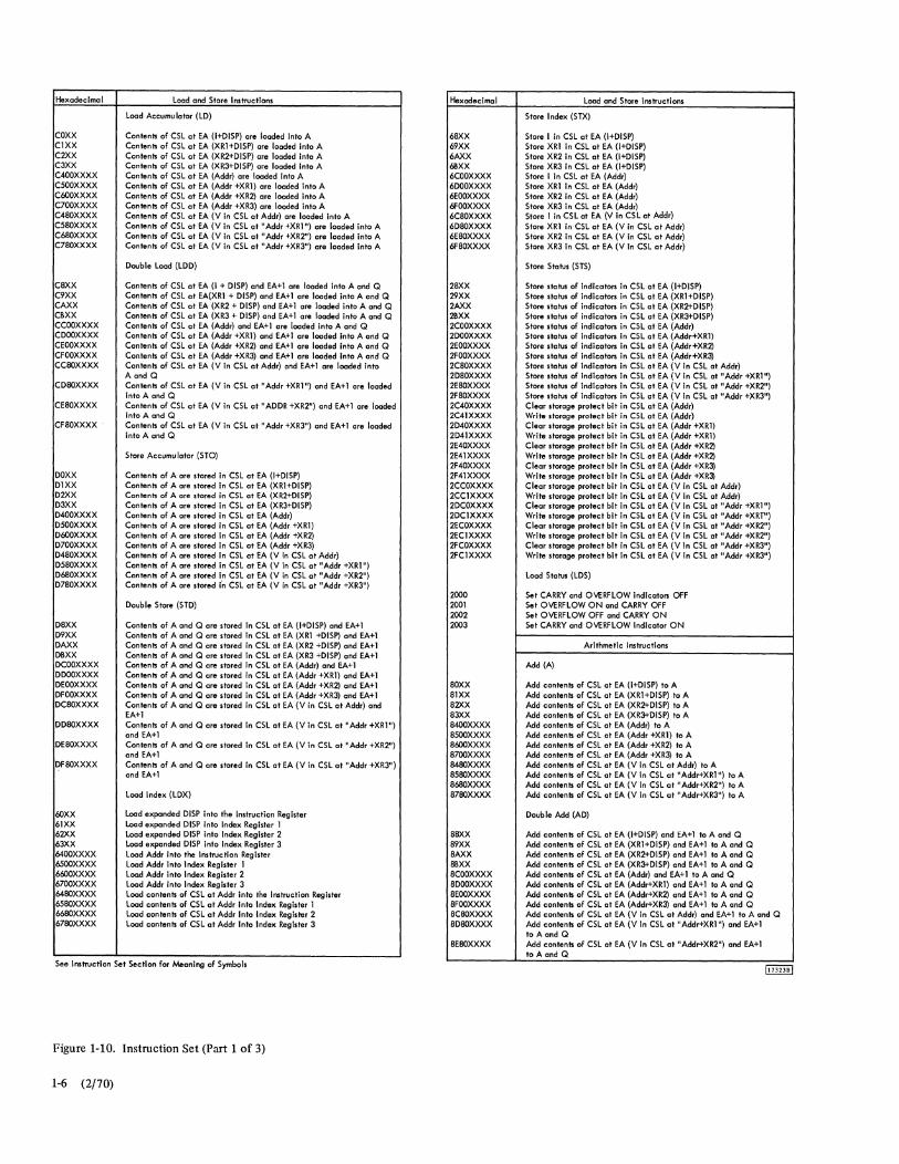
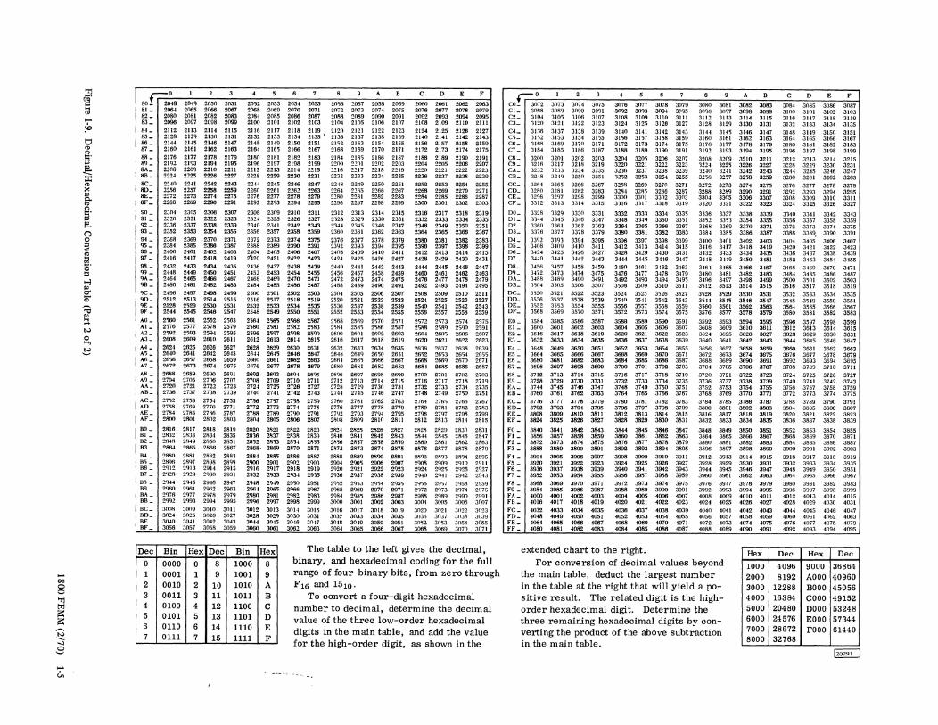
Hexadecimal Load and Store Instructions Hexadecimal Load and Store Instructions
Load Accumu lator (LD) Store Index (STX)
COXX Contents of CSL at EA (I+DISP) are loaded Into A 68XX Store I in CSL at EA (I+DISP) C]XX Contents of CSL at EA (XR]+DISP) are loaded into A 69XX Store XR] in CSL at EA (I+DISP) C2XX Contents of CSL at EA (XR2+DISP) are loaded into A 6AXX Store XR2 in CSL at EA (I+DISP) C3XX Contenb of CSL at EA (XR3+DISP) are looded into A 68XX Store XR3 in CSL at EA (I+DISP) C400XXXX Contents of CSL at EA (Addr) are loaded into A 6COOXXXX Store I in CSL at EA (Addr) C500XXXX Contents of CSL at EA (Addr +XR1) are loaded into A 6DOOXXXX Store XRl In CSL at EA (Addr) C600XXXX Contents of CSL at EA (Addr +XR2) are loaded into A 6EOOXXXX Store XR2 in CSL at EA (Addr) C700XXXX Contents of CSL at EA (Addr +XR3) are loaded into A 6FOOXXXX Store XR3 in CSL at EA (Addr) C480XXXX Contents of CSL at EA (V in CSL at Addr) are loaded Into A 6C80XXXX Store I in CSL at EA (V in CSL at Addr) C580XXXX Contents of CSL at EA (V in CSL at tlAddr +XRl ") are loaded into A 6D80XXXX Store XRI in CSL at EA (V in CSL at Addr) C680XXXX Contents of CSL at EA (V in CSL at tlAddr +XR2t1) are loaded into A 6E80XXXX Store XR2 In CSL at EA (V in CSL at Addr) C780XXXX Contents of CSL ot EA (V in CSL at IIAddr +XR3t1 ) are loaded into A 6F80XXXX Store XR3 In CSL at EA (V In CSL at Addr)
Double Load (LDD) Store Statu. (STS)
C8XX Contents of CSL at EA (I + DISP) and EA+l are loaded into A and Q 28XX Store .talus of Indicators in CSL at EA (i+DISP) C9XX Contents of CSL at EA(XRI + DISP) and EA+] are loaded into A and Q 29XX Store .tatu. of Indicators in CSL at EA (XR]+DISP) CAXX Contents of CSL at EA (XR2 + DISP) and EA+I are loaded into A and Q 2AXX Store statu. of Indicators In CSL at EA (XR2+DISP) CSXX Contents of CSL at EA (XR3 + DISP) and EA+I are loaded Into A and Q 2BXX Store .tolus of indicators in CSL at EA (XR3+DISP) CCOOXXXX Contents of CSL at EA (Addr) and EA+I are loaded into A and Q 2COOXXXX Store .tatu. of Indicators in CSL at EA (Addr) CDOOXXXX Contents of CSL at EA (Addr +XRl) and EA+] are loaded into A and Q 2DOOXXXX Store stahJs of indicators In CSL at EA (Addr+XR1) CEOOXXXX Contents of CSL at EA (Addr +XR2) and EA+I are loaded into A and Q 2EOOXXXX Store status of indicators in CSL at EA (Addr+XR2) CFOOXXXX Contents of CSL at EA (Addr +XR3) and EA+I are loaded Into A and Q 2FOOXXXX Store status of indicators in CSL at EA (Addr+XR3) CC80XXXX Contents of CSL at EA (V In CSL at Addr) and EA+I are loaded into 2C80XXXX Store .tatu. of Indicators in CSL at EA (V In CSL at Addr)
A and Q 2D80XXXX Stare status of Indicators in CSL at EA (V In CSL at "Addr +XR1") CD80XXXX Contents of CSL ot EA (V in CSL at "Addr +XRll1) and EA+l are loaded 2E80XXXX Stare status of indicators in CSL at EA (V in CSL at I1Addr +XR2")
Into A and Q 2F80XXXX Store status of indicators in CSL at EA (V In CSL at "Addr +XR3") CE80XXXX Contents of CSL at EA (V In CSL at "ADDR +XR2") and EA+I are loaded 2C40XXXX Clear .tora~e protect bit in CSL at EA (Addr)
into A and Q 2C41XXXX Write storage protect bit in CSL at EA (Addr) CF80XXXX Content> of CSL at EA (V In CSL at "Addr +XR3") and EA+] are loaded 2D40XXXX Clear .torage protect bit in CSL at EA (Addr +XRl)
into A and Q 2D4]XXXX Write .torage protect bit in CSL at EA (Addr +XR1) 2E40XXXX Clear .torage protect bit In CSL at EA (Addr +XR2)
Store Accumu lator (STO) 2E41XXXX Write .torage protect bit In CSL at EA (Addr +XR2) 2F40XXXX Clear .torage protect bit in CSL at EA (Addr +XR3)
DOXX Contents of A are .tored in CSL at EA (I+DISP) 2F41XXXX Write .toroge protect bit In CSL at EA (Addr +XRJ) D1XX Content> of A are .tored In CSL at EA (XRI+DISP) 2CCOXXXX Clear .torage protect bit In CSL at EA (V In CSL at Addr) D2XX Contents of A are stored in CSL at EA (XR2+DISP) 2CC]XXXX Write .torage protect bit in CSL at EA (V In CSL at Addr) D3XX Content> of A are .tored in CSL at EA (XR3+DISP) 2DCOXXXX Clear .torage protect bit In CSL at EA (V In CSL at "Addr +XR1") D400XXXX Content> of A are .tored In CSL at EA (Addr) 2DC]XXXX Write storage protect bit in CSL at EA (V in CSL at "Addr +XRr') D500XXXX Contents of A are stored in CSL at EA (Addr +XRl) 2ECOXXXX Clear .toroge protect bit in CSL at EA (V In CSL at "Addr +XR2") D600XXXX Content> of A are .tored in CSL at EA (Addr +XR2) 2ECIXXXX Write storage protect bit in CSL at EA (V in CSL at "Addr +XR2") D700XXXX Content> of A are .tored in CSL at EA (Addr +XR3) 2FCOXXXX Clear storage protect bit in CSL at EA (V in CSL at "Addr +XR3 11 )
D480XXXX Contents of A are .tored In CSL at EA (V in CSL at Addr) 2FCIXXXX Write storage protect bit In CSL at EA (V In CSL at IIAddr +XR31l )
D580XXXX Contents of A are stored in CSL at EA (V in CSL at tlAddr +XRlll) D680XXXX Contents of A are stored in CSL at EA (V in CSL at "Addr +XR2t1) Load Status (LDS) D780XXXX Contents of A are stored i'n CSL at EA (V in CSL at tlAddr +XR3 11 )
2000 Set CARRY and OVERFLOW Indicators OFF Double Store (STD) 2001 Set OVERFLOW ON and CARRY OFF
2002 Set OVERFLOW OFF and CARRY ON D8XX Contents of A and Q are .tared In CSL at EA (I+DISP) and EA+] 2003 Set CARRY and OVERFLOW indicator ON D9XX Contents of A and Q are .tored in CSL at EA (XR] +DISP) and EA+I DAXX Contents of A and Q are .tored in CSL at EA (XR2 +DISP) and EA+l Arithmetic Instructions DSXX Contents of A and Q are .tored In CSL at EA (XR3 +DISP) and EA+] DCOOXXXX Contents of A and Q are stored in CSL at EA (Addr) and EA+l Add (A) DDOOXXXX Content> of A and Q are .tored In CSL at EA (Addr +XRl) and EA+] DEOOXXXX Contents of A and Q are .tored in CSL at EA (Addr +XR2) and EA+I 80XX Add contents of CSL at EA (I+DISP) to A DFOOXXXX Contents of A and Q are .tored In CSL at EA (Addr +XR3) and EA+I 81XX Add content> of CSL at EA (XR]+DISP) to A DC80XXXX Contents of A and Q are stored in CSL at EA (V in CSL at Addr) and 82XX Add content> of CSL at EA (XR2+DISP) to A
EA+] 83XX Add contents of CSL at EA (XR3+DISP) to A DD80XXXX Contents of A and Q are stored in CSL at EA (V in CSL at tlAddr +XRl") 8400XXXX Add content> of CSL at EA (Addr) to A
and EA+l 8500XXXX Add content> of CSL at EA (Addr +XRl) to A DE80XXXX Contents of A and Q are stored in CSL at EA (V in CSL at "Addr +XR2") 8600XXXX Add content> of CSL at EA (Addr +XR2) to A
and EA+l 8700XXXX Add content> of CSL at EA (Addr +XR3) to A DF80XXXX Contents of A and Q are .tored In CSL at EA (V in CSL at "Addr +XR3") 8480XXXX Add content> of CSL at EA (V In CSL at Addr) to A
and EA+I 8580XXXX Add contents of CSL at EA (V In CSL at "Addr+XR1") to A 8680X)(XX Add content> of CSL at EA (V In CSL at "Addr+XR2") to A
Load Index (LDX) 8780XXXX Add content> of CSL at EA (V In CSL at "Addr+XR3") to A
60XX Load expanded DISP into the Indruction Register Double Add (AD) 61XX load expanded DISP into Index Register 1 62XX Load expanded DISP into Index Register 2 88XX Add contents of CSL at EA (i+DISP) and EA+l to A and Q 63XX Load expanded DISP into Index Register 3 89XX Add contents of CSL at EA (XRI+DISP) and EA+I to A and Q 6400XXXX Load Addr into the Instruction Register 8AXX Add content> of CSl at EA (XR2+DISP) and EA+] to A and Q 6500XXXX Load Addr into Index Register 1 BBXX Add content> of CSL at EA (XR3+DISP) and EA+] to A and Q 6600XXXX LOQd Addr into Index Register 2 8COOXXXX Add contents of CSL at EA (Addr) and EA+l to A and Q 6700XXXX Load Addr into Index Register 3 8DOOXXXX Add content> of CSL at EA (Addr+XRl) and EA+] to A and Q 6480XXXX Load contents of CSL at Addr into the Instruction Register 8EOOXXXX Add content> of CSL at EA (Addr+XR2) and EA+ 1 to A and Q 6580XXXX Load contents of CSL at Addr Into Index Register 1 8FOOXXXX Add content> of CSL at EA (Addr+XR3) and EA+] to A and Q 6680XXXX Load contents of CSL at Addr Into Index Register 2 8C80XXXX Add content> of CSL at EA (V in CSL at Addr) and EA+I to A and Q 6780XXXX Load contents of CSL at Addr Into Index Register 3 8D80XXXX Add content> of CSL at EA (V In CSL at "Addr+XR1") and EA+l
to A and Q 8E80XXXX Add content> of CSL at EA (V In CSL at "Addr+XR2") and EA+I
toAandQ See Instruction Set Section for Iv\eaning of Symbols
Figure 1-10. Instruction Set (Part 1 of 3)
1-6 (2/70)
Hexadecimal Arithmetic Instructions Hexadecimal Arithmetic Instructions
BFSOXXXX Add contents of CsL at EA (V in CsL at "Addr+XR3") and EA+I Logical Or (OR) toA and Q
E8XX OR contents of CSL at EA (I+DISP) with A Subtract (5) E9XX OR contents of CSL at EA (XRI+DISP) with A
EAXX OR contents of CsL at EA (XR2+DISP) with A 90XX Subtract contents of CsL at EA (I+DlsP) from A 91XX Subtract contents of CsL at EA (XRI+Dlsp) from A 92XX Subtract contents of CsL at EA (XR2+DlsP) from A 93XX Subtract contents of CsL at EA (XR3+DlsP) from A 9400XXXX Subtract contents of CsL at EA (Addr) 'rom A 9S00XXXX Subtract contents of CsL at EA (Addr+XR1) from A 9600XXXX Subtract contents of CsL at EA (Addr+XR2) from A 9700XXXX Subtract contents of CsL at EA (Addr+XR3) from A 94SOXXXX Subtract contents of CsL at EA (V In CsL at Addr) from A
EBXX OR contents of CsL at EA (XR3+DISP) with A ECOOXXXX OR content. of CSL at EA (Addr) with A EDOOXXXX OR contents of CSL at EA (Addr+XRI) with A EEOOXXXX OR contents of CSL at EA (Addr+XR2) with A EFOOXXXX OR contents of CSL at EA (Addr+XR3) with A ECSOXXXX OR contents of CsL at EA (V in CSL at Addr) with A EDSOXXXX OR contents of CSL at EA (V in CSL at "Addr+XRI") with A EE80XXXX OR contents of CSL at EA (V in CSL at "Addr+XR2") with A EFSOXXXX OR contents of CsL at EA (V in CSL at "Addr+XR3") with A
9SSOXXXX Subtract contents of CsL at EA (V in CsL at "Addr+XRl ") from A 96SOXXXX Subtract contents of CsL at EA (V in CsL at "Addr+XR2") from A Logical Exclu.lve Or (EOR) 97SOXXXX Subtract contents of CsL at EA (V In CsL at "Addr+XR3") from A
FOXX EOR contents of CsL at EA (I+DISP) with A Double Subtract (sD) FIXX EOR contents of CSL at EA (XRI+DISP) with A
F2XX EOR contents of CSL at EA (XR2+DISP) with A 98XX Subtract contents of CsL at EA (I+DlsP) and EA+l from A and Q 99XX Subtract contents of CsL at EA (XR1+DlsP) and EA+l from A and Q 9AXX Subtract contents of CsL at EA (XR2+DlsP) and EA+l from A and Q 98XX Subtract contents of CsL at EA (XR3+DlsP) and EA+l from A and Q 9COOXXXX Subtract contents of CsL at EA (Addr) and EA+ 1 from A and Q 9 DOOXXXX Subtract contents of CsL at EA (Addr+XRI) and EA+l from A and Q 9EOOXXXX Subtract contents of CsL at EA (Addr+XR2) and EA+l from A and Q 9FOOXXXX Subtract contents of CsL at EA (Addr+XR3) and EA+l from A and Q 9CSOXXXX Subtract contents of CSL at EA (V In CsL at Addr) and EA+l from
F3XX EOR contents of CSL at EA (XR3+DISP) with A F400XXXX EOR contents of CSL at EA (Addr) with A FSOOXXXX EOR contents of CSL at EA (Addr+XRI) with A F600XXXX EOR contents of CSL at EA (Addr+XR2) with A F700XXXX EOR contents of CSL at EA (Addr+XR3) with A F480XXXX EOR contents of CSL at EA (V in CSL at Addr) with A FSSOXXXX EOR contents of CSL at EA (V in CSL at "Addr+XRI ") with A F680XXXX EOR contents of CSL at EA (V In CSL at "AddrtXR2") with A F780XXXX EOR contents of CSL at EA (V In CsL at "AddrtXR3") with A
A and Q 9DSOXXXX Subtract contents of CsL at EA (V in CsL at "Addr+XRl ") and Shift In,tructlon.
EA+l from A and Q 9ESOXXXX Subtract contents of CsL at EA (V In CsL at "Addr+XR2") and Shift Left Logical A (SLA)
EA+l from A and Q 9F80XXXX Subtract contents of CsL at EA (V in CsL at "Addr+XR3") and
EA+l from A and Q
10'X Contents of A .hift left the number of .hlft counts In DISP 1100 Contents of A shift left the number of shift counts in XRl 1200 Contents of A shift left the number of shift counts Tn XR2
Multiply (M) 1300 Contents of A .hlft left the number of .hlft counts In XR3
AOXX Multiply contents of CsL at EA (I+DlsP) by A Shift Left Logical A & Q (SLT) A1XX Multiply contents of CsL at EA (XRI+Dlsp) by A A2XX Multiply contents of CSL at EA (XR2+DISP) by A 10'X Contents of A and Q .hlft left the number of ,hlft counts In DISP A3XX Multiply contents of CSL at EA (XR3+DISP) by A 1180 Contents of A and Q .hlft left the number of .hlft counts In XRl A400XXXX Multiply contents of CSL at EA (Addr) by A 1280 Contents of A and Q .hlft left the number of .hlft counts i" XR2 ASOOXXXX Multiply contents of CSL at EA (Addr+XR1) by A 1380 Contents of A and Q .hlft left the number of ,hlft counts In XR3 A600XXXX Multiply contents of CSL at EA (Addr+XR2) by A A700XXXX Multiply contents of CSL at EA (Addr+XR3) by A Shift Left And Count A (SLCA) A4SOXXXX Multiply contents of CSL at EA (V In CSL at Addr) by A ASSOXXXX Multiply contents of CSL at EA (V In CsL at "Addr+XRI ") by A lO'X Contents of A shift left the number of shift counts in DISP A6SOXXXX Multiply contents of CSL at EA (V in CSL at "Addr+XR2") by A 1140 Contents of A shift left the number of shift counts in XRl A7SOXXXX Multiply contents of CSL at EA (V in CSL at "Addr+XR3") by A 1240 Contents of A shift left the number of shift counts in XR2
1340 Contents of A shift left the number of shift counts in XR3 Divide (D)
Shift Left And Count A & Q (sLC) A8XX Divide A and Q by contents of CSL at EA (I+DlsP) A9XX Divide A and Q by contents of CSL at EA (XRI+DISP) 10'X Contents of A and Q ,hift left the number of .hllt counts In DISP AAXX Divide A and Q by contents of CsL at EA (XR2+DlsP) I1CO Contents of A and Q shift left the number of shift counts In XRl ABXX Divide A and Q by contents of CsL at EA (XR3+DISP) 12C0 Contents of A and Q .hlft I.ft the number of ,hlft counts In XR2 ACOOXXXX Divide A and Q by contents of CSL at EA (Addr) 13CO Contents of A and Q shift left the number of shift counts in XR3 ADOOXXXX Divide A and Q by contents of CSL at EA (Addr+XR1) AEOOXXXX Divide A and Q by contents of CSL at EA (Addr+XR2) Shift Right Logical A (SRA) AFOOXXXX Divide A and Q by contents of CSL at EA (Addr+XR3) ACSOXXXX Divide A and Q by contents of CSL at EA,(V in CSL at Addr) 18'X Contents of A .hift right the number of ,hlft counts In DISP ADSOXXXX Divide A and Q by contents of CSL at EA(V in CSL at "Addr+XR1" 1900 Contents of A .hlft right the number of ,hift counts in XRI AESOXXXX Divide A and Q by content. of CSL at EA(V in CSL at "Addr+XR2" IAOO Contents of A ,hlft right the number of ,hlft counts In XR2 AFSOXXXX Divide A and Q by contents of CSL at EA(V in CSL at "Addr+XR3" IBOO Contents of A .hlft right the number of .hlft counts In XR3
Logical And (AND) Shift Right A & Q (SRT)
EOXX AND contents of CsL at EA (I+DISP) with A EIXX AND contents of CSL at EA (XRI+DlsP) with A E2XX AND contents of CSL at EA (XR2+DlsP) with A E3XX AND contents of CSL at EA (XR3+DISP) with A
18'X Contents of A and Q .hift right the number of .hift counts in DlsP 19S0 Contenh of A and Q shift right the number of shift counts in XRl IA80 Contents of A and Q shift right the number of shift counts in XR2 lB80 Contents of A and Q shift right the number of shift counts in XR3
E400XXXX AND contents of CSL at EA (Addr) with A ESOOXXXX AND contents of CSL at EA (Addr+XRI) with A Rolate Right A & Q (RTf) E600XXXX AI,D contents of CSL at EA (Addr+XR2) with A E700XXXX AND contents of CSL at EA (Addr+XR3) with A lS'X Contents of A and Q rotate right the number of counts In DISP E4SOXXXX AND contents of CsL at EA (V In CSL at Addr) with A 19CO Contents of A and Q rotate right the number of counts In XRl ES80XXXX AND contents of CSL at EA (V in CSL at "Addr+XRI ") with A lACO Contents of A and Q rotate right the number of counts In XR2 E6SOXXXX AND contents of CSL at EA (V In CSL at "Addr+XR2") with A lBCO Contents of A and Q rotate right the number of counts In XR3 E7SOXXXX AND contents of CSL at EA (V In CSL at "Addr+XR3") with A
Figure 1-10. Instruction Set (Part 2 of 3)
IIlOO I,'EMM (2/70) 1-7
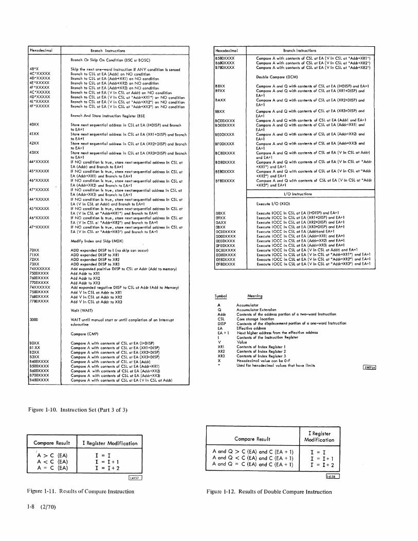
HexadecImal Branch Instructions
Branch Or Skip On Condition (BSC or BOSC)
4S·X Skip the next one-word instruction if ANY condition 15 sensed 4C·XXXXX Branch to CSL at EA (Addr) an NO condition 40·XXXXX Branch to CSL at EA (AddrtXR1) on NO condition 4E·XXXXX Branch to CSL at EA (AddrtXR2) on NO condition 4F"XXXXX Branch to CSL at EA (AddrtXR3) on NO condition 4C·XXXXX Branch to CSL at EA (V in CSL at Addr) on NO condition 40·XXXXX Branch to CSL at EA (V In CSL at "AddrtXR1") on NO condltlan 4E·XXXXX Branch to CSL at EA (V In CSL at "AddrtXR2") on NO condition 4F·XXXXX Branch to CSL at EA (V In CSL at "AddrtXR3") on NO condition
Branch And Store Instruction Register (BSt)
40XX Store next sequential oddress in CSL ot EA (I+0ISP) and Branch to EA+l
41XX Stare next sequential addre .. in CSL at EA (XRI+OISP) and Branch to EA+l
42XX Stare next sequential address In CSL at EA (XR2+0ISP) and Branch to EA+1
43XX Stare next sequential addre .. In CSL at EA (XR3+0ISP) and Branch to EA+1
44·XXXXX If NO condition 15 true, store next sequentIal oddress In CSL at EA (Addr) and Branch to EM 1
4S·XXXXX If NO condition Is true, store next sequentIal address In CSL at EA (Addr+XR1) and Branch to EA+1
46·XXXXX If NO condItion Is true, store next sequential address In CSL at EA (AddrtXR2) and Branch to EA+ 1
47'XXXXX If NO condition Is true, store nextsequentlal address In CSL at EA (AddrtXR3) and Branch to EA+1
44·XXXXX If NO condition is true, store next sequential address in CSL at EA (V In CSL at Addr) and Branch to EA+1
4S·XXXXX If NO condition is true, store next sequential address In CSL at EA (V In CSL at "Addr+XR1") and Branch to EA+1
46·XXXXX If NO condition Is true, store next sequentIal address In CSL at EA (V In CSL a: "AddrtXR2") and Branch to EA+1
47·XXXXX If NO condition 15 true, store next sequential address In CSL at EA (V In CSL at "Addr+XR3") and Branch to EA+1
Modify Index and Skip (MOX)
70XX ADD expanded OISP to I (no skip can occur) 71XX ADD expanded DISP to XR1 72XX ADD expanded DISP ta XR2 73XX ADD expanded DISP to XR3 74XXXXXX Add expanded positive DISP to CSL at Addr (Add ta memory) 7SOOXXXX Add Add. to XR1 7600XXXX Add Addr to X R2 7700XXXX Add Addr to X R3 74XXXXXX Add expanded negative DISP to CSL at Addr (Add to Memary) 7S80XXXX Add V In CSL at Add. to XR1 7680XXXX Add V In CSL at Addr to XR2 n80XXXX Add V In CSL at Addr to XR3
Walt (WAIT)
3000 WAIT until manual start or until completIon of on Interrupt subroutine
Compare (CMP)
BOXX Compare A with contents of CSL at EA (I+DISP) B1 XX Compare A with cantents af CSL at EA (XR1+DISP) B2XX Compqre A with cantents of CSL at EA (XR2+DISP) B3XX Campare A with contents of CSL at EA (XR3+DISP) B400XXXX Campare A with cantents of CSL at EA (Addr) BSooXXXX Compare A with contents of CSL at EA (Addr+XR1) B600XXXX Campare A with contents of CSL at EA (AddrtXR2) B700XXXX Campare A with contents of CSL at EA (AddrtXR3) B480XXXX Compare A with contents of CSL at EA (V In CSL at Addr)
Figure 1-10. Instruction Set (Paxt 3 of 3)
Compare Result I Register Modification
i A>C (EA) I = 1 A<C (EA) 1 = 1+1 A = C (EA) I = 1+ 2
Fil,'llre 1-11. Results of Compare Instruction
1-8 (2/70)
Hexadecimal Branch Instructions
BS80XXXX B680XXXX B780XXXX
B8XX B9XX
BAXX
BBXX
BCOOXXXX BDOOXXXX
BEOOXXXX
BFOOXXXX
BC80XXXX
BD80XXXX
BE80XXXX
BF80XXXX
OSXX D9XX OAXX OBXX OCOOXXXX ODOOXXXX OEOOXXXX OFOOXXXX OC80XXXX ODSOXXXX OE80XXXX OF80XXXX
Symbol
A Q Add. CSL DISP EA EA + 1 I V XRl XR2 XR3 X
Compare A with contents of CSL at EA (V In CSL at "AddrtXR1") Compare A with cantents of CSL at EA (V In CSL at "AddrtXR2") Compare A with contents of CSL at EA (V In CSL at "AddrtXR3")
Double Compare (DCM)
Compare A and Q with cantents of CSL at EA (I+DISP) and EA+1 Compare A and Q with contents af CSL at EA (XR1+DISP) and EM1 Compare A and Q with contents of CSL at EA (XR2+DISP) and EA+1
Compare A and Q with contents af CSL at EA (XR3+DISP) and EM1 Campare A and Q with contents of CSL at EA (Addr) and EA+1 Compare A and Q with contents of CSL at EA (AddrtXR1) and EA+1 Compare A and Q with contents of CSL at EA (AddrtXR2) and EA+1 Compare A and Q with cantents of CSL at EA (AddrtXR3) and EA+1 Compare A and Q with contents of CSL at EA (V In CSL at Addr) and EA+l Compare A and Q with cantents of CSL at EA (V In CSL at "Addr +XR1 ") and EA+1 Compare A and Q with contents of CSL at EA (V In CSL at "Addr +XR2") and EA+1 Compare A and Q with contents of CSL at EA (V In CSL at "Addr +XR3") and EA+1
I/O Instructions
Execute I/O (XIO)
Execute 10CC In CSL at EA (I+DISP) and EA+1 Execute 10CC In CSL at EA (XR1+DISP) and EA+1 Execute 10CC In CSL at EA (XR2+DISP) and EA+1 Execute 10CC In CSL at EA (XR3+DISP) and EA+1 Execute 10CC In CSL at EA (Addr)and EA+1 Execute 10CC In CSL at EA (AddrtXR1) and EA+1 Execute 10CC In CSL at EA (AddrtXR2) and EA+1 Execute 10CC in CSL at EA (AddrtXR3) and EA+1 Execute 10CC In CSL at EA (V in CSL at Addr) and EA+1 Execute 10CC In CSL at EA (V in CSL at "AddrtXR1") and EM1 Execute 10CC In CSL ot EA (V In CSL at "AddrtXR2") and EA+1 Execute 10CC In CSL at EA (V In CSL at "Addr+XR3") and EA+1
Accumulator Accumulator Extension Contents of the address portIon of a two-word Instruction Core storage location Contents of the displacement portion of a one-word Instruction Effective address Next higher address from the effective address Contents of the Instruction Register Value Contents of Index Register 1 Contents of Index Register 2 Contents of Index Register 3 Hexadecimal value can be O-F Used for hexadecimal values that have limits
1 Register Compare Resu It Modification
A and Q > C (EA) and C (EA + 1) I = 1 A and Q < C (EA) and C (EA + I) I = 1+ 1 A and Q = C (EA) and C (EA + I) 1 = I+ 2
Figure 1-12. Results of Double Compare Instruction
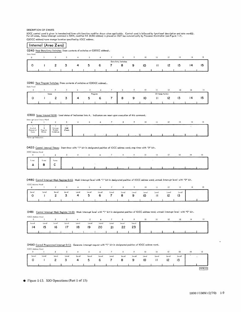
DESCRIPTION OF CHARTS
loce control word is given in hexadecimal form with function modifier shown when applicable. Control word is followed by functional description and data word(s}. for all areas, Sense Interrupt command is 03XXi modifier XX (ILSW address) is placed on OUT bus automatically by Processor-Controller (see Figure 1-7).
C(IOCe address)=core storage location specified by loce address.
I Internal (Area Zero) I 0240 Read Doto Entry Switches: Store contents of switches at c(loce address) •
Ooto Word
10 " 12 13 14
Dota Entry Swilc::hes
0 2 3 4 5 6 7 8 9 10 II 12 13 14
I I I I I I I I I I I I I I
0260 Read Program Switches: Store contents of switches ot c{lace address).
Data Wo,d
10 " 12 13 14
Sense Program CE Sense Switch
0 I 2 3 4 5 6 7 8 9 10 II 12 13 14
I I I I I I I I I I I I
0300 Sense Internol ILSW: Load status of indicators into A. Indicators are reset upon execution of this command.
Intelrupt Level Statu> Word
o I 10 " 12 13 14
Involld B Storoge CAR Operotlo" Register Protect Check
Code Panty Vlolotlon
1 I I . 1 I . 'I 1 J J. * Interrupt Indlcotors
0420 Control Interval Timers: Stort timer with 11111 bit in designated position of 10CC oddress word; stop timer with liD" bit.
10CC Address Word
10 " 12 13 14
B I '~I : : Timer
0480 Control Interrupt Mask Register 0-13: Mask interrupt level with "III bit in designated position of lace address word; unmask interrupt level with "Oil bit.
10CC Address Word
10 " 12 13 14
Level level Level Level Level Level Level Level Level Level Level Level Level level
o 23456789 10 II 12 13
I I I I I I I I I I I I I
0481 Control Interrupt Mosk Register 14-23: Mask interrupt level with "I" bit in designated position of 10CC address word; unmask interrupt level with "0" bit.
loce AddreS5 WOld
10 " 12 13 14
Level Level Level Level Level Level Level Level Level Level
14 15 16 17 18 19 20 21 22 23
_I
I
J
I I I I I I I I I i J. .. .1
04AO Control Programmed Interrupt 0-13: Generate interrupt request with "III bit in designated position of loce address word.
loce Address Word
10 " 12 13 14
Level Level Level level Level Level Level Level Level Level Level Level Level Level
o 2 3 4 5 6 7 8 9 10 II 12 13
I I L I J I I I !
• Figure 1-13. XIO Operations (Part 1 of 15)
15
15
15
15
15
15
15
15
15
[HOU FEMM (2/70) 1-9
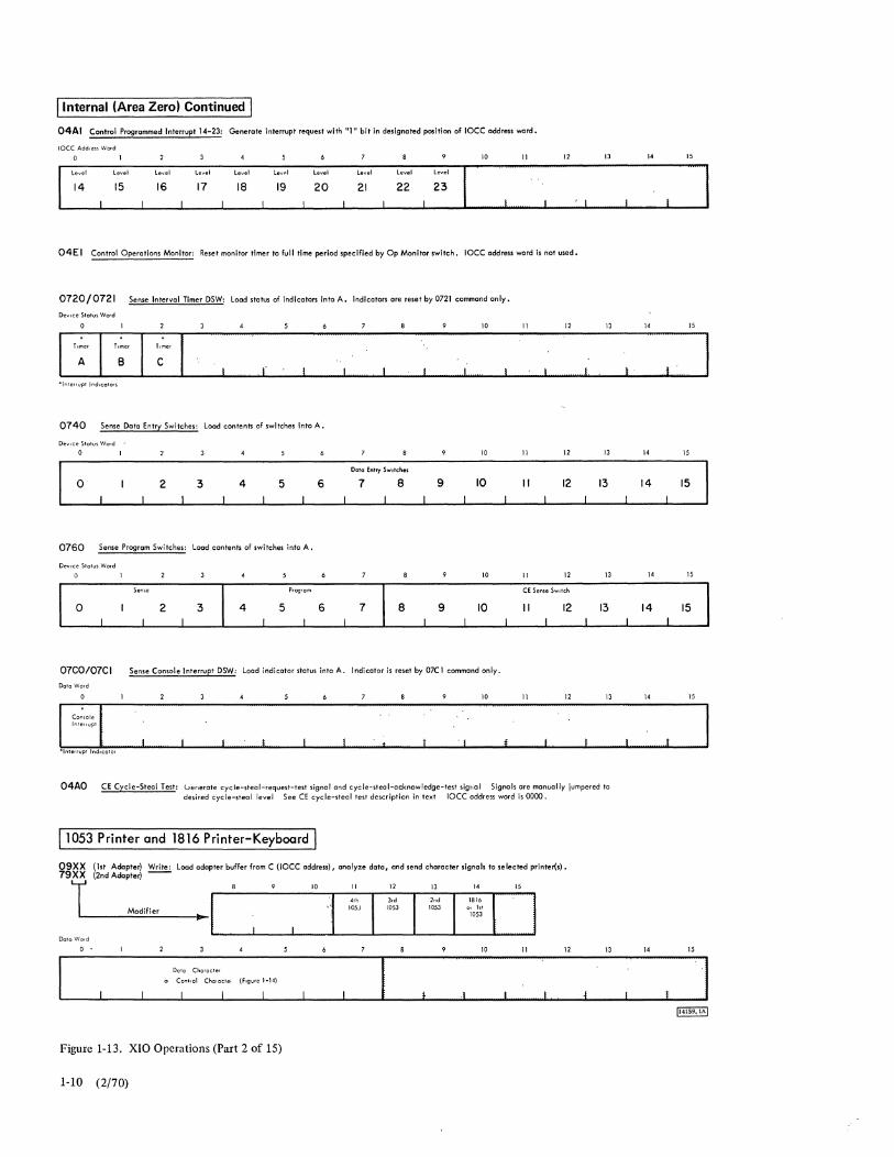
I Internal (Area Zero) Continued I 04AI Control Programmed Interrupt 14-23: Generate interrupt request with "1" bit in designated position of loce address word.
loce Add, ell Word
10 II J2 13
le"el Level level level Level Levrl level Level Level Level
14 15 16 17 18 19 20 21 22 23
I I I I I I I I I .J I ... 1
04EI Control Operations Monitor: Reset monitor timer to full time period specified by Op Monitor switch. loce address word is not used.
Seme Program CE Sense SWitch
0 I 2 3 4 5 6 7 8 9 10 II 12 13 I I I I I I I I I I I
07GO/07GI Sense Console Interrupt DSW: Load indicator status into A. Indicator is reset by 07el command only.
Data Wo,d
10 II J2 13
1o,"""" I C,m,l, I : : : -Interrupt IndlC:otof
04AO CE Cycle-Steal Test: Generate cycle-steol-request-test signol and cycle-steal-acknowledge-test sigrlol Signals are manually jumpered to desired cycle-steal level See CE cycle-steal test description in text 10CC address word is 0000.
1053 Printer and 1816 Printer-Keyboard
09XX 79XX
(1st Adapter) ~ load adopter buffer from C (loee addreu), analyze data, and send character signals to selected printer(s). (2nd Adapter)
T 10 " Modifier
Data WOld
o •
Data Character
01 Contlol O"Olacte, (Figure IMI41
Figure 1-13. XIO Operations (Part 2 of 15)
1-10 (2/70)
12
3,d 1053
13 14
10
: :
15
" 12 13
14 15
.1
14 15 J ..i
14 15
14 15
: : I
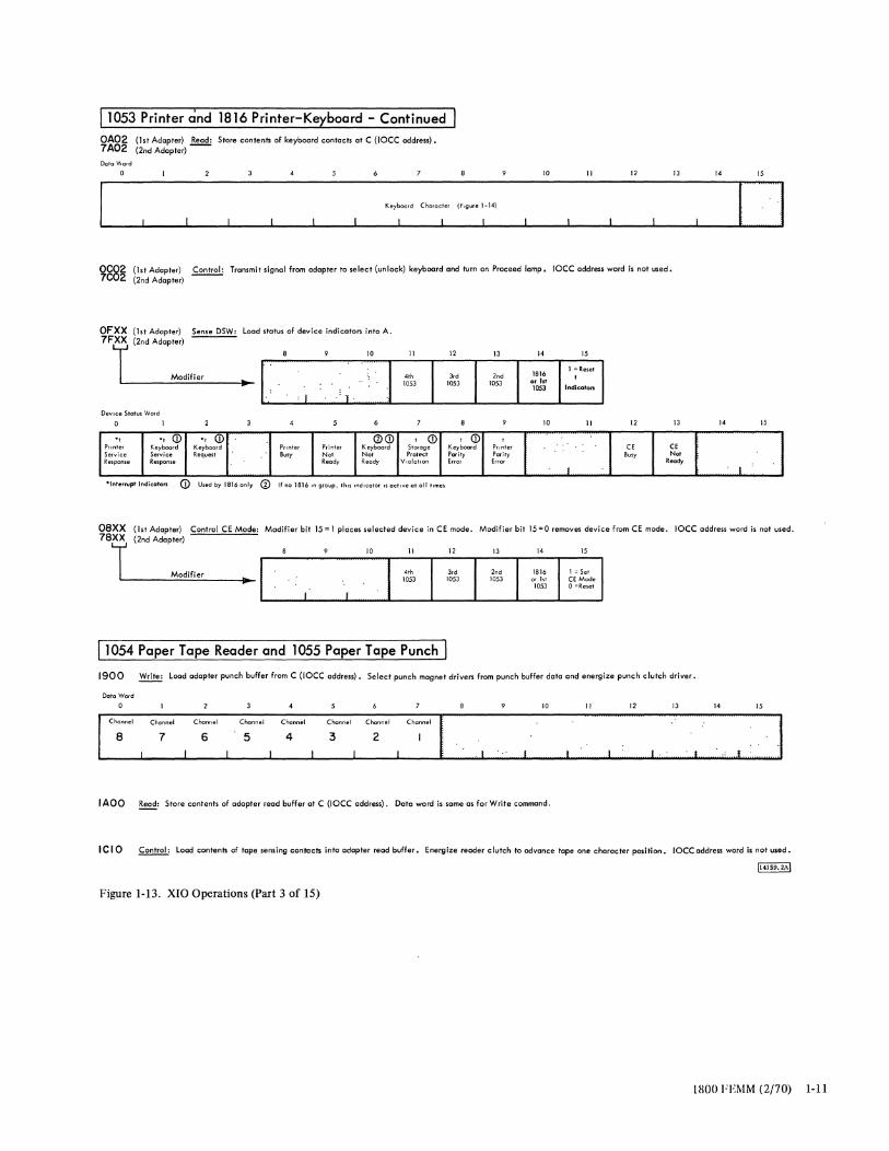
1053 Printer ~nd 1816 Printer-Keyboard - Continued
OA02 (lst Adopter) Reod: Store contents of keyboord contacts at e (lace address). 7 A02 (2nd Adapter) --
Dolo Vvord
Keyboard Charader (Flgl,ne 1-14)
10 lJ 12 13
OC82 (1st Adapter) Control: Transmit signal from adapter to select (unlock) keyboard and turn on Proceed lamp. loce address word is not used. 7C 2 (2nd Adapter)
OFXX (1st Adapter) Sense DSW: Load status of device indicators into A.
7FT 1'-' ".':;,;., • ,...------....,.-,..1-0-...... -1~-~-~-..... -,~-~d-3 - ...... -,-;5-:;-..,..-+-~-~-...... ,n-,d'-;,R-~:-:~-I.., DeVice Status Word
°1 Printer
Service Response
°1 CD Keyboard Service Response
°1 CD Keyboard Request
:! : 'I'
Prmter Printer Busy Nol
Ready
<YCD 1 CD Keyboard Storage Nol ProtE'et Ready Violation
-'nterrvpt Indicators CD Used by 1816 only 0 If no 1816 In group, thIS indIcator IS active 01 all times
10 lJ
1 CD 1 Keyboard PrlOter Pority Pority Error Error
12 13
CE C' Busy Nol
Ready
14 15
II
14 15
.1
08XX 78r (1st Adapter)
(2nd Adapter) Control CE Mode: Modifier bit 15 = 1 places selected device in CE mode. Modifier bit 15 =0 removes device from CE mode. lace address word is not used.
10 lJ 12 13 14 15
Modifier 41h J,d 20d 1816 1 = Set
~ 1053 1053 1053 or 1st CE Mode 1053 o =Reset
" I
1054 Paper Tape Reader and 1055 Paper Tape Punch
1900 Write: Load adapter punch buffer from C (lace address). Select punch magnet drivers from punch buffer doto and energize punch clutch driver.
Data Word 10 lJ 12 13 14 15
Chonnel Channel Channel Channel Channel Chonnel Channel Chonnel
8 7 6 5 4 3 2 I I I I , , , I , I I J,
I ADO ~: Store contents of adopter read buffer at C (lace address). Doto word is same as for Write command.
lei 0 Control: load contents of tope sensing contacts into adapter read buffer. Energize reader clutch to advance tope one character position. IOCCoddress word is not used.
114159.21\1
Figure 1-13. XIO Operations (Part 3 of 15)
1800 FEMM (2/70) 1-11
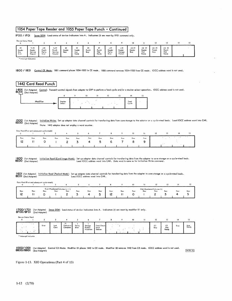
11054 Paper Tape Reader and 1055 Paper Tape Punch - Continued 1
IFOO IIFOI ~: load status of device indicators into A. Indicators (t) are reset by IFOl command only.
DeVice Status Word
1 10 11 12 13 14 15
PT "t PT t PT "I PT PT PT PT PT t PT tPT CE PT CE PT CE PT CE PT Reader Reader Punch Punch Reader Reader Punch Punch Reeder Reader Reoder Reader Punch Punch Any Service Parity Service Busy Not Busy Not Parity Storoge Busy Not Busy Not Error Request Error Request Ready Reedy Error Protect R~dy R~dy
* " Interrupt Indicators
1800/1801 Control CE Mode: 1801 command place. 1054-1055 in CE mode. 1800 command remove. 1054-1055 from CE mode. 10CC address word is not used.
11442 Card Read Punch 1 14XX (1st Adapter) ~: Transmit control signals from adapter to CRP to perform a feed cycle and/or a stocker select operation. loce address word is not used.
8C'1"L: __ (_2_nd __ A_d_OP_t_~_:_d_if_ie_r ______ ~_ 10 11 12 13 14 15
Stocker Feed I I .. Select Cycle
1
1500 (Is t Adopter) 8000 (2nd Adopter)
Initialize Write: Set up adopter data channel controls for transFerring data From core storage to the adopter on a cycle-steal basis. Load 10CC address word into CAR.
Note: 1442 adopter does not employ a word counter.
Dola Word (Fltsl and subsequent cycle-steals)
1 10 11 12 13 14 15
Row Row Row Row Row Row Row Row Row Row Row Row
12 " 0 2 3 4 5 6 7 8 9 I I I I I I I I I I I :I' . J. . .J
1600 (1st Adopter) Initialize Read (Cord Image Mode): Set up adapter data channel controls for transFerring data From the adopter to core storage on a cycle-steal basis. SEOO (2nd Adopter) Load 10CC address word into CAR. Data word is some as for Initialize Write command.
1601 (1st Adapter) Initialize Read (Packed Mode): Set up adopter dota channel controls for transferring data From the adopter to core storage on a cycle-steal basis. 8EOI (2nd Adopter) Load 10CC address word into CAR.
Data Word (FHst ond subsequent cycle-steah) o I 2 10 11 12 13
Even-Numbered Columns (n + 1) Odd-Numbered Columns (n) Row Row Row Row Row Row Row Row Row Row Row Row Row Row
12 I " o
1 I 2
I 3
I 4 5
I 12
I " I o
I I 2 I 3
1700/1701 (1st Adopter) Sense DSW: Load status of device indicators into A. Indicators (t) are reset by modifier 01 only. 8FOO/8FOI (2nd Adopter)
DeVice Status- Ward
Error
" Interrupt Indicator
last Card
·t Operation Complete
t Parity Error
t Storage Protect Violation
Feed Check Read Stotlan
I t· .
10 11 12 13
CE CE Busy Not
R~dy
' . .('
14
Row
4 I
14
Busy
1000/1001 (1st Adopter) Control CE Mode: Modilier 01 places 1442 in CE mode. Modifier 00 removes 1442 from CE mode. 10CC address word is not used. 8800/8801 (2nd Adapter)
Figure 1-13. XIO Operations (Part 4 of 15)
1-12 (2/70)
15
Row
I 5
15
Not Ready
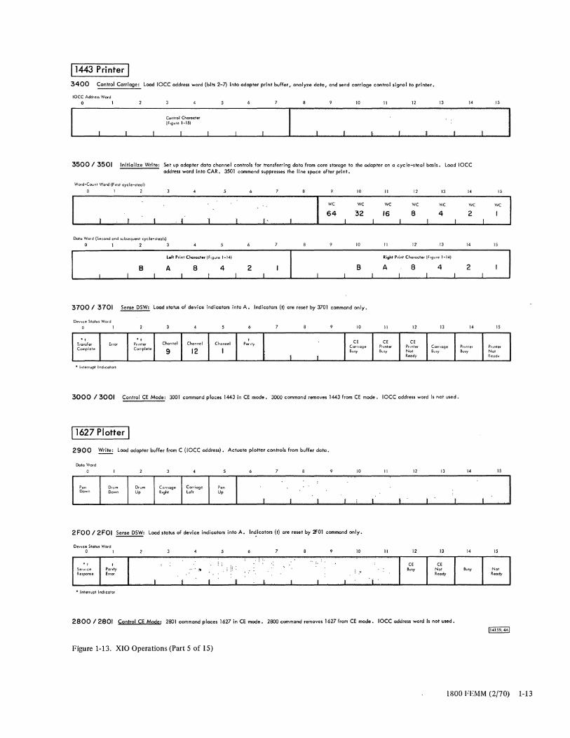
11443 Printer
3400 Control Carrloge: load IOCe address word (bits 2-7) into adapter print buffer t analyze dota, and send carriage control signal to printer.
loce Addrels Word
I
Control (harotter (F,gure 1-15)
10 II 12 13 14
3500/ 3501 Initialize Write: Set up adopter doto channel controls for transferring doto from core storage to the adapter on a cycle-steal basis. Load loce oddreu word Into CAR. 3501 command suppresses the line space after print.
Word-Count Word (FIrSt tyde-steal)
o I 2 10 II 12 13
WC WC WC wC WC
64 32 16 8 4
Data Word (Second and }ubsequent cycle-steals)
10 1\ 12 13
Left Print Character (F,gure 1-14) Right Print Character (F,gure 1-14)
B A 8 4 2 B A 8 4 I I I I I 1 I I I I I I I
3700 13701 Sense DSW: Load stotus of device indicators into A. Indicators (t) ore reset by 3701 command only.
DeVIce Status Word
10 II 12 13
"I T ronsfer Error Complete
"I 1 CE CE CE Printer Channel Chonnel Channel Parity Complete Carriage Printer Printer Carriage
9 12 Busy Busy Nol Busy
t j Ready
* Interrupt Indlcaton
3000 /3001 Control CE Mode: 3001 command places 1443 In CE mode. 3000 command removes 1443 from CE mode. loce address word is not used.
11627 Plotter I 2900 Write: Load adopter buffer from C (IOCC address). Actuate plotter controls from buffer data.
Data Word
10
p," Drum Drum Carnage Carrioge p," Down Down Up Right left Up
J j I. I
2FOO / 2FOI Sense DSW: Load status of device indicators into A. In~icators (t) ore reset by 2FOl command only.
DeVice Status Word o
"I 1 ServlI;:e Parity Response Error
* Interrupt Indicator
.~
.1 ! ! . *
\0
.. , ..
: ,Y
l I I .. 1.
II 12 13
1 ! I
\I 12 13
CE CE Busy Nol
Ready
i·
2800/2801 Control CE Mode: 2801 command places 1627 in CE mode. 2800 command removes 1627from CE mode. 10CC address word Is not used.
Figure 1-13. XIO Operations (Part 5 of 15)
1
14
WC
2
14
2
14
Printer Busy
14
14
Busy
15
15
wc
15
I
15
Printer Nol Readv
15
I
15
Nol Ready
1800 FEMM (2/70) 1-13
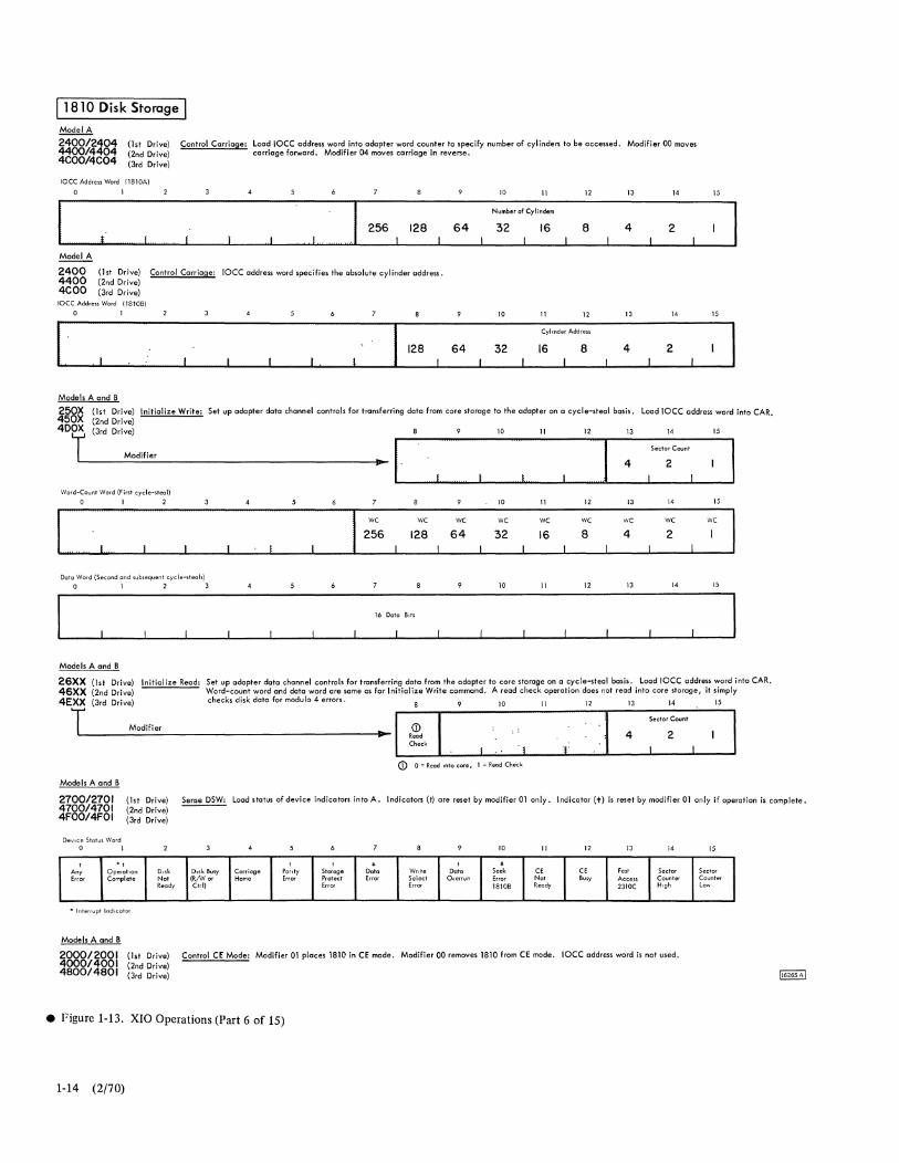
1810 Disk Storage
Model A
2400/2404 440014404 4COO/4C04
{lst Drive) (2nd Drive) (3rd Drive)
loce Address Word (181OA)
Model A
Control Carriage: Load lace address word into adopter word counter to specify number of cylinders to be accessed. Modifier 00 moves carriage forward. Modifier 04 moves carriage in reverse.
10 11 12 13 14
J Number of Cylinders
256 128 64 32 16 8 4 2 j
2400 4400
(I st Drive) Control Carriage: lace address word specifies the absolute cylinder address. (2nd Drive)
4COO (3rd Drive) loce Address Word (181OB)
0 1 10 11 12 13 14
Cylinder Address
128 64 32 16 8 4 2
Models A and B
15
15
250X 450X
4Dr (1st Drive) Initialize Write: Set up adapter data channel controls for transferring data from core storoge to the adapter on a cycle-steal basis. Load lace address word into CAR. (2nd Drive) (3rd Drive) 10 11 12 13 14 15
Modifier t Sector Count
~ ~. ____ ~ ____ ~ ____ ~ __ ~~ __ ~ ___ 4 __ ~_2 __ ~ ____ ~ Word-Count Word (Fir$t cycle-steal)
o 1 2 10 11 12 13 14 15
we we we we we we we we we
256 128 64 32 16 8 4 2 I. 1 1 I 1 I I 1 I I I I I I
Dolo Word (Second and subsequenl cycle-sleol$)
o 1 2 3 10 11 12 13 14 15
16 Dolo Blls
Models A and B
26XX 46XX 4EXX
(1st Drive) Initialize Read: Set up adapter data channel controls for transferring data from the adapter to core storage on a cycle-steal basis. Load 10CC address word into CAR. (2nd Drive) Word-count word and data word are same as for Initialize Write command. A read check operation does not read into core storage, it simply (3rd Drive) checks disk data for modulo 4 errors. 10 II 12 13 14 15
T Modifier
Models A and B
CD R~d
Check I
<D 0 == Read Into core, I '" Read Check
1 I Sector Count
4 2
2700/2701 4700/4701 4FOO/4FOI
(1st Drive) (2nd Drive) (3rd Drive)
~ Load status of device indicators into A. Indicators (t) are reset by modifier 01 only. Indicator (t) is reset by modifier 01 only if operation is complete.
Dev1ce Statu$ Word o 1
, Aoy Error
" Operat1on Complete
.. Interrupt Indicator
Models A and B
Disk Disk Busy Carriage Not (R/'N or Home Reody Ctrl)
, Panty Error
, Storage Protecl Error
. Data Error
Write Select Error
, Data
Overrun
10 11 12 13 14
• Seek eE eE Fast Sector Error Not Busy Access Counter 18108 Ready 231OC High
~ggg~~ggl (lst Drive) Control CE Mode: Modifier 01 places 1810 in CE mode. Modifier 00 removes 1810 from CE mode. 10CC address word is not used.
4800/4801 (2nd Drive) (3rd Drive)
• figure 1-13. XIO Operations (Part 6 of 15)
1-14 (2/70)
15
Sector Counter low
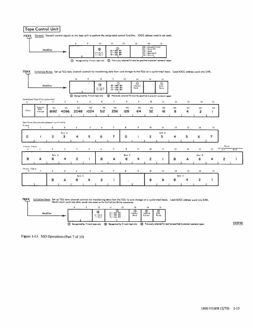
I Tape Control Unit I 74TL: __ e_o_n_tr_o_,~_:"_~_,:_~_, '_t_c_on_t_rO_I,.~ .. lg_nOIS to the tope unit to perform the designated control function. loee address wand Is not used.
10 II 12 13 14 15
00 "'SJPBPI
000 '" ReWind Unload @ 001 .. Write 1M
010;; Erose o "'TU 0 01 "" 200 BPI all " Backspace
·1 I =TU I 10: 5561 BPI 100'" Re .... md
CD Recognized by 7-tJUck tape only Q) Previously selected tu mud b. speciflftl to prevent cornmond relect
CD Recognized by 7-track tape only @ Pnwloudy selected TU must b. specified to prevent command reject
Word-Count Word (First cycle-steal)
o I 2 10 II 12 13 14 15
Suppress we we we we we we we we we we we we we we Choln EOT
8192 2048 1024 512 256 128 64 32 16 Interrupt 4096 8 4 2 I I I I I I I I I I I I I I
Data Words (Second and subsequent cycle-steals)
9-track 0 10 II 12 13 14 15
Byte A Byte B
0 2 3 4 5 6 7 0 2 3 4 5 6 7
7-trock,3-Byte Porl'Y
0 10 II 12 13 14 15 0-' 8-15
Byte A Byte C Byte 0
8 A 8 4 2 I 8 A 8 4 2 I 8 A 8 4 2 I I I I I I I I I I I I I I
7-hock, 2-Byte 0 10 II 12 13 14 15
Byte A I : I Byte B
8 A 8 4 2 B A 8 4 2
76XX Initialize Read: Set up TeU data channel controls for transferring data from the leU to core storage on a cycle-steal basis. Load loce address word into CAR. Word-count word and data words are same as for Initialize Write command.
10 II 12 13 14 15
Modifier @ 00 =800~P1 <D R.2l &
<D 3 Bytes/ Even
0'" TU 0 01 .: 200 BPI W",d Correct POrlty I'" TU I 10.: 556 BPI
t I (j) Recognlud by 7-traclc tap. only a> Recognized by 9-track tope only a> Previously •• Iect" TU must be specified to prevent cCNftmCInd reject
Figure 1-13. XIO Operations (Part 7 of 15)
lHOO FEMM (2/70) 1-15
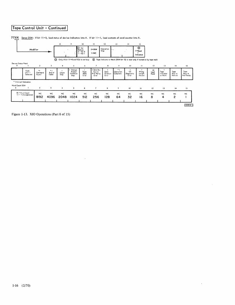
ITape Control Unit - Continued I
77TL: __ s_e_",_e_D_S_W_: _1_f_b_.,t_l_l_=_O_' ... I~oad status of device indicators into A. If bit 11 = 1, load contents of word counter into A.
10 11 12 13 14 15
~4set O-OSW Operation @ Modifier ddress
~ : 0 = TU 0 Slop I-Reset
I::: TU I l=we t
I I Indicators
@ Only If bit 11 =0 cnd TeU is not busy @ Tape Indicator or Mark (OSW bit 13) Is r •• t only if fumed on by tope mork
DeVice Status Word 0 10 11 12 13 14 15
Tape ., ., I t Storage I I Data Bus I ., I I AI I Protect Tape Out or Doto Operotion eE Wrong Lead Tape Tope Tape
Unit I Command End of Chain Violation Dala P-C Parity Overrun Complete Diagnostic Length Point Indicator Busy or Busy or Selected Relect Tobie Stop Stop Error ErrOl" Error Error Record or Mark ReWind Not Ready
* Interrupt Indicators
WOld Count DSW
0 10 11 12 13 14 15
00 = True Count we we we we we we we we we we we we we we 11 = 1'5 Complement
8192 4096 2048 1024 512 256 128 64 32 16 8 4 2 I I I I I I I I I I I I I I
114159.611
Figure 1-13. XIO Operations (Part 8 of 15)
1-16 (2/70)
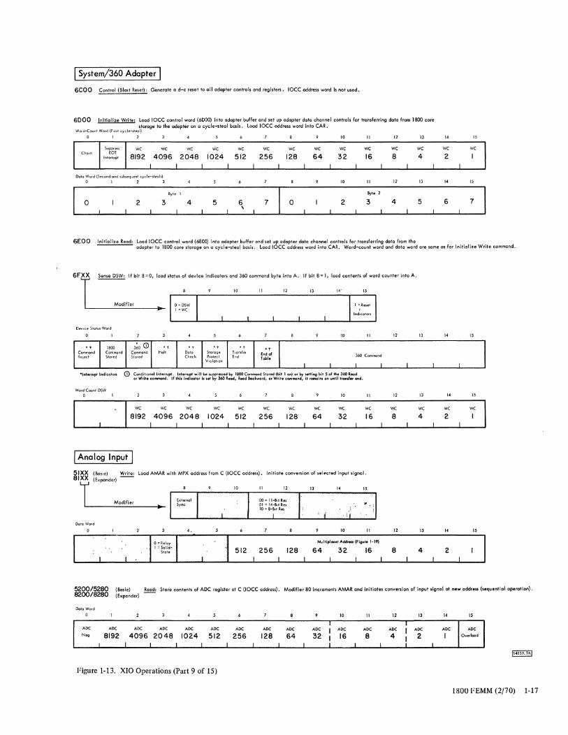
I System/360 Adapter I 6cao Control {Blast Reset}: Generate a d-c reset to all adopter controls and registers. loce address word is not used.
6000 Initialize Write: Load loce control word (6000) Into adapter buffer and set up adopter data channel controls for transferring data from 1800 core storage to the adapter on a cycle-steal basis. Load loce address word Into CAR.
Word-Count Word (First c:yc;le-sleol)
o 1 2 3 4 5 6 10 II 12 13
Suppress we we we we we we we we we we we we Choln 'DT 8192 4096 2048 1024 512 256 128 64 32 16 8 4 Interrupt
1 1 1 1 1 I I I I I I I
Dato Word (Second and subsequent cyde-steal5) 0 I 2 3 10 \I 12 13
Byte 1 Byte 2
0 2 3 4 5 6 7 0 2 3 4 5 ,
14 15
we we
2 I I
14 15
6 7
6EOO ,Initialize Read: Load loce control word (6EOO) into adapter buffer and set up adapter dota channel controls for transferring doto from the adapter to 1800 core storage on a cycle-steal bosis. Load loce address word into CAR. Word-count word and data word are same as for Initialize Write command.
6F X Sense DSW: If bit 8 =0, load status of device indicators and 360 command byte into A. If bit 8 = 1, load contents of word counter into A.
Modifier
DeVice StatusWOtd
0+ 1800 Command Caml!'ll;Jnd Relect Stored
Word Count DSW o
3~0 <D Caml!'ll;Jnd Stored
we
0'" DSW I =WC
°t • t Halt 00 ••
Check
we we
8192 4096 2048 I 1 I I
I Analog Input I
°t Star<lge Pratect
Violation
we
1024 I
10 II 12 13 14' 15
II,' .... • Ind!cators
10 \I
ot ot Tlonsfel End of 360 Cammand ',d Tabl.
I I 1 I
10 \I
we we we we we we
512 256 128 64 32 16 I I I I I 1
51XX (BaSIC) Write: LoadAMAR with MPX address from e (Ioee address). Initiate conversion of selected input signal. 81 XX (Expander)
T 10 \I 12 13 14 15
Modifier External 00:: II-Bit Res ~ .:/ ~ Sync 01:. 14-811 Res
10::: 8-81t Res
I I ' i .,', Data Word
4. 10 \I
o ::Relay Multlpl •• r Add,.. (figure 1-19) I:: Solid-
512 256 128 64 32 16 Siale
I I I I 1 1 1 1 1
12
I
12
we
8 1
12
8 I
13 14 15
I I
13 14 15
we we we
4 2 I' 1
13 14 15
4 2 I 1 I
5200/5280 (Basic) Read: Store contents of ADC register at C (Ioce address). Modifier 80 increments AMAR and initiates conversion of input signal at new address (sequential operation). 8200/8280 (Expander)
Data Word
ADe
N .. ADC
8192 I
ADC ADC ADC ADC
4096 2048 1024 512 1 1 1
Figure 1-13. XIO Operations (Part 9 of 15)
ADC ADC ADC
256 128 64 I I I
10 \I 12
ADC ;
4 I ADC
32 ADC
8 I I
13
ADC
2 1
14
ADC
I
15
ADC
Overload
1800 FEMM (2/70) 1-17
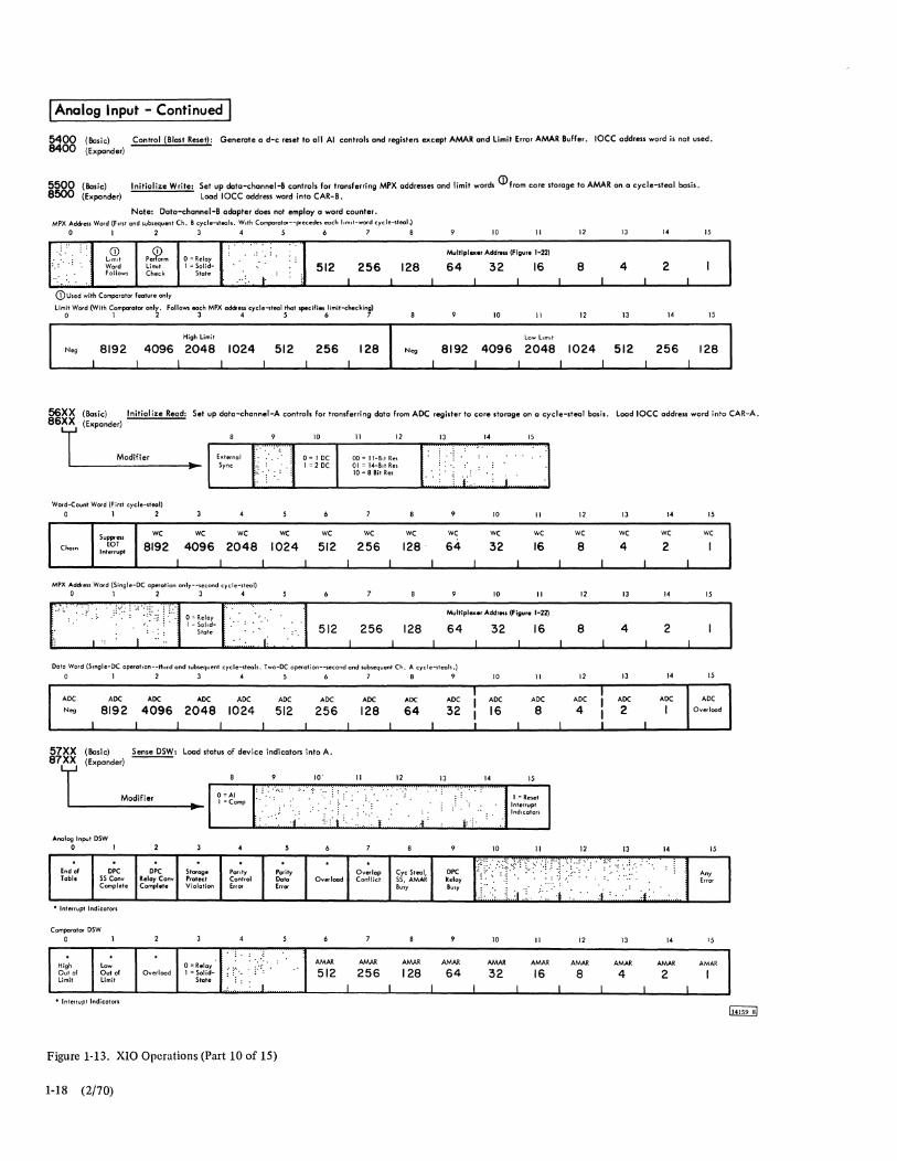
I Analog Input - Continued I 5400 (Basic) Control (Blosl Resel): Generale a d-c resello all AI conlrol. and regi.lers ""cepl AMAR and limil Error AMAR Buffer. 10CC addr ... word i. nol used. 8400 (Expander)
5500 (Ba.ic) 8500 (Expander)
Initialize Write: Set up data-channel-B controls for transferring MPX addresses and limit words (])'rom core storage to AMAR on a cycle-steal basis. Load 10CC add res. word inlo CAR-B.
Note: Data-channel-B adapter does not employ a word counter. MPX Address Word (flnt and subsequent Ch. a cycle-steals. With Comparalor--pecedes each limit-word cycle.."teal~ 012345678
~ :
:,:' .:
" . ~ ..
CD Limit W~d Follows
perCPorm limit Check
<D Used with Comparator feature only
o ;;.Relay 1 = Solid
Stale .":' t .
512 256 I
Limit Word (With COrnpcn'otor only. Follows eoch MPX address cycle ... teal that specifies limil-checking) o 1234567
High limit
Neg 8192 4096 2048 1024 512 256 128 I I I I I I I
128 I
Neg
I
I
10 11 12
Multlplex.r Addreu (fi"ur. 1-22)
64 32 16 8 I i I
10 11 12
Low Llm,t
8192 4096 I
2048 1024 I I
13 14 15
4 2 I I I
13 14 15
512 256 128 I I I
!56XX (Basic) Initialize Read: Set up dato-channel-A controls for transferring data from ADC regider to core storoge on 0 cycle-steel basis. Lood 10CC address word into CAR-A. 81 ''''_,~,;. "_," 0.': OC ~. ".0 .:' " " "
i L------------I~~ Sync I = 2 DC 01 = 14-Blt Res
•.•. : 10 = 8 Bit Res ..
Word-Count Word (First cycle-steal)
o 1 2 10 II
SUpp-e5S we we we we we we we we we we
Cham EOT 8192 4096 2048 1024 512 256 128 - 64 32 16 Interrupt
I I i .1 I I I I I
MPX Addreu Word (Single-DC operotion only·-second cycle-steal) o 1 2 3 4 10 II
,,':,' 0:. Relay 1 - Solid
Stote
Multlplex.r Addreu (flgur. 1-22)
512 256 128 64 I'" I I I I I
Doto Word (Single-DC operohon--thlrd ond subsequent cycle-deals. Two-DC operation--second and subsequent Ch. A cycle-steah.)
o 123456789
ADC Neg
ADC ADC
8192 4096 I I I
ADC ADe ADe
2048 1024 512 I I I
ADe :
32 I ADC
256 ADC
128 ADC
64 I I I I
32 16 I
10 II
ADC ADC
16 8 I
57XX (Basic) ~: Load .Ialus of device indicolors inlo A.
87~LX __ (E_x_p_on_d_e_r~_O_d_if_ie_r ____ ~_ r-O-=-A-,---r:~:~.~~~~~~,~~,~ .. ~;~O~:.~!w,~:,w.~I~I~~ .. ~.~1~~~.~~~13~~~~14~~_'_=_R.~I:_'-' ~ I=eomp ".' .f'. 'j.:.r,:.:::.::!. ,l: .' l:'.!.' :~~~:~i.'"
Analog Input DSW o 10 II
I
I
I
12
we
8 I
12
8 I
12
ADC :
41
12
13
we
4 I
13
4 I
13
ADC
2 I
13
End of Table
ope 55 Conv Complete
oPe Relay Conv Complete
Storage Protect Violation
Panty Control error
Parity Do •• Error
Overlop Conflict
eyc Steal. 55, AMIAR BUIY
':':;::':~';~'S':\:':'.r.:"]'~~::~~':' ~" ~'.'::'.:' "~~.: ::r.. . .....
• Interrupt Indieotors
Comparator OSW
o
High Out of Limit
low Out of Limit
• Interrupt Indicators
Overload 0= Relay 1 = Solid
State
. ,.:
Figure 1-13. XIO Operations (Part 10 of 15)
1-18 (2/70)
Overload
AMAR AMAR AMAR
512 256 128 I I I
.:'-:: j:J ':'. '.::. : ... : .... ! .. ..,: .. :4:''': :f:'
10 11 12 13
AMAR AMAR AMAR AMAR AMAR
64 32 16 8 4 I I I I I
14
we
2
14
2
14
ADC
I
14
14
AMAR
2
I
I
I
15
we
I
15
15
ADe Overload
15
Aor error
'5
AMAR
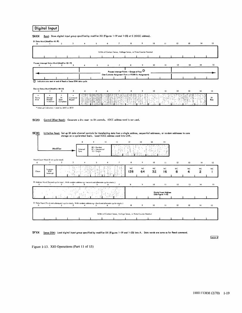
I Digital Input I 5AXX ~: Siore digitol inpul group specified by modifier XX (Figures 1-19 and 1-20) 01 C (lOCC address).
Dl Data Word (Modlfl.r 40-7F)
o I
I I I I
Process Interrupt Status Word (Modifier 02-19) o I 2 3
I I I I I
CD Indicaton 0 ... reset at end of R«ret or Sens. DSW data cycle
Device Status Word (Modifier 00-01) o I 2
Panty Error
Storage Protect Violation
01 S=" Complete
* Interrupt Indicators ~ reset by SA01 or SFOI
16 Bits of Contact Sen5e. Voltage Sense, Of Pulse Counter Readout
I 1 1 I I I
Process Interrupt POj~h - Group; of Four <D (S .. CUltom.r Assignment Form or FURl for Assignments)
I I I I I I
5C20 Control (Biasi Re.el): Generale a d-c resel 10 01 conlrol •• 10CC address word is nol used.
10 II 12 13
I I I
10 II 12 13
I I I I
10 II 12 13
Initialize Read: Set up 01 data channel controls for transferring data from a stngle address, sequential addresses, or random addresses to core .torage on a cycle-steal basi •• Load 10CC address word into CAR.
Modifier
Word-Count Word (First cycle-deal)
o I 2
Chom Suppress
EOT Interrupt
Externol Sync
00 = Random 01 '" Sequenhal 10'" Single
I
10 II
:. : ::" -: j":. . :: : :.: ~ .. , ~:: ~ ~ t '. t. '. i: .: ~:'. : :·.~l i(',~ ";.j j~':l '.~ ('.li,: r, '
01 Address Word (Second cycle-steal. With random addresslng--second and alternate cycle-steals.) 0123456
.1 . I
01 Oota Word (Thud and subsequent cycle-steals. With random addresslng--thlrd and alternate cycle-steals.) 01234567
12
we 128
13 14 15
10 II
we we we 64 32 16
I I I I
10 II
Digital Input Add .... (5" Figure 1-20)
I
10 II
16 Bits of Contact Senre, Voltoge Sense, ()( Pulse Counter Readout
I J I I I 1 I 1 I I I
12 13
we we 8 4
I
12 13
12 13
I
5FXX ~: Load digitol inpul group .pecified by modifier XX (Figur .. 1-19 and 1-20) inla A. Dolo words are same a. for Read command.
Figure 1-13. XIO Operations (Part 11 of 15)
14
I
14
I
14
14
we 2
I
14
14
l
I
I
I
I
15
15
..
15
01 Busy
IS
we I
15
15
1HOO FEMM (2/70) 1-19
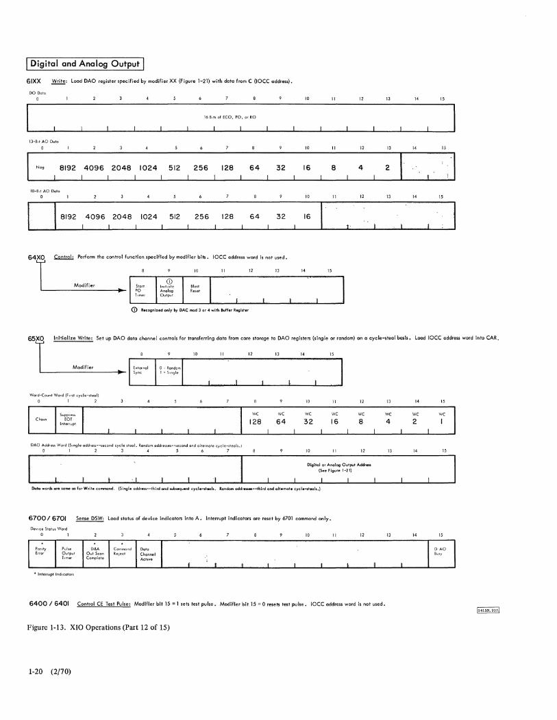
Digital and Analog Output
61XX Write: Load DAO register specified by modifier XX (Figure 1-21) with dota from e (lace address).
DO Data
o
13-8.,AO Doto
N ••
I
10-B,t AO Data 0
8192
I I BI92
4096 2048 I 1 I
4096 2048
16 Blh of ECO, PO, or RO
1024 512 256 128 64 32 I I I I I
1024 512 256 128 64 32
64XO Control: Perform the control function spectfled by modifier bits. loee address word Is not used.
T 10 11 12 13
Modifier Stort CD
Blast Initiate ~ PO Anolog Reset
Timer Output
I I
CD Recognized only by DAC mad 3 or 4 with Buffer Register
I
10 11 12 13 14 15
10 11 12 13 14 15
16 8 4 2 I I I I t
10 11 12 13 14 15
16 I : 14 15
.. I
~Lo __ ln_lt_~_I_~_~_~_d_:_~_~_s_et_u_p_D~A~O_dra_:_,_~_~_:_M~II_:_O_~_:_~_~_:TOlr_t_~_:_:_~_rr_I_~_do_l:_O~f_ro_m_~_r_:_s_._~_g_e_t_~_:_A_o_:_r_eg_i_:_B_(_SI'_~_I_e_:_:_r,OI~_·_~~~~-m~~--.-m. - ~ Sy", 1 0 500,1. ! . .
Word-Count Word (First cycle-steal)
o 1 2
Suppress Chain EOT
Interrupt
J I J I I
DAO Address Word (Single oddress--second cycle steal. Random oddrenes--second and alternole cycle-s'etlls.1 01234567
. L .J . I
we we 128 64
I
I
I
I
10 11 12
we we we 32 16 8
I I
10 11 12
Digital or Analog Outp.Jt Address (SllIe Figure 1-21)
I I Data words are lame as far Write command. (Single address--third and subsequent cycle-steals. Random address.--thlrd and alternate cycle-steals.)
6700/6701 ~ Lood stotus of device indicators into A. Interrupt Indicators are reset by 6701 command only.
DeVice Statui Word
Ponty Error
Pulse Output Timer
* Interrupt Indicators
D&A Command Data Out Scan Relect Channel Complete Active
10
I I I
11 12
1
1
*
6400/6401 Control eE Test Pulse: Modifier bit 15 = 1 sets test pulse. Modifier bit 15 = 0 resets test pulse. lace oddress word is not used.
Figure 1-13. XIO Operations (Paxt 12 of 15)
1-20 (2/70)
13 14
we we 4 2
I
13 14
I
13 14
I
1
1
15
we I
15
15
o AO Busy
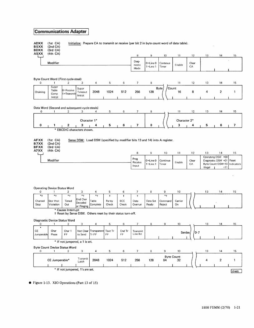
ICommunications Adapter I
ADXX B5XX BDXX A5XX
(1st CAl (2nd CAl (3rd CAl (4th CAl
Initialize: Prepare CA to transmit or receive (per bit 2 in byte count word of data table).
8 9 10 11
I Modifier Dlag-
O=Line 0 Continue nostlc
1 =lIne 1 Timer Enable
Mode
Byte Count Word (First cycle-steal) o 1 2 3 4 5 6 7 8 11
Suppr Suppr Byte)
Chaining Table O=Receive
Timeout 2048 1024 512 256 128 Camp 1 =Transmit
I ( Intrpt Intrpt
I I I I
Data Word (Second and subsequent cycle-steals) 0 1 2 3 4 5 6 7 8 11
12
Clear CA
12
8
12
Character 1 * (( Character 2*
0 2 3 4 5 6 7 0 3 4
* EBCDIC characters shown.
AFXX (1st CAl Sense DSW: Load DSW (specified by modifier bits 13 and 14) into A register. B7XX (2nd CAl BFXX (3rd CAl A7XX (4th CAl
8 9
I Prog Modifier Receive
O=Line 0
Input 1 =Line 1
Operating Device Status Word o 1 2 3 4 5 6 7 8
*t *t *t *t *t t t t
Channel Star Prot Timed End Char
Table Panty BCC Data Data Set Decoded
Stop Violation Out or Ringing
Complete Check Check Overrun Ready
* Causes Interrupt t Reset by Sense DSW. Others reset by their status turn-off.
Diagnostic Device Status Word o 1 2 3 4 5 6 7 8
* CE Char Char 1 Not Clear Transparent Text Tr End Tr Transmit Jumperable Phase FF to Send Tr FF FF FF Line Bit
* If not jumpered, a 1 is set.
Byte Count Device Status Word o 1 2 3
CE Jumperable* Transmit Latch
4 5 6 7 8
2048 1024 512 256 128
I
I I I I I I I I * If not jumpered, 1 's are set .
• Figure 1-13. XIO Operations (Part 13 of 15)
10 11 12
Continue Enable
Clear Timer CA
9 10
*t ( Command Carrier Reject On
9 10
Serdes
I I
9 10
Byte Count 64 32
I
13 14 15
I I
13 14 15
4 2
13 14 15
5 6 7
13 14 15
Operating DSW =00 Diagnostic DSW =01 Reset Byte Count DSW=10 Indicators Illegal I =11
13 14 15
: 13 14 15
13 14 15
1800 FEMM (2/70) 1-21
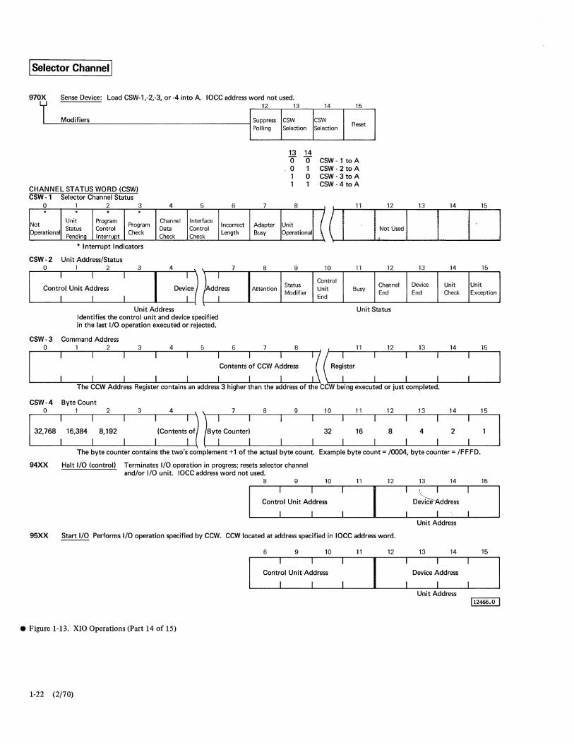
I Selector Channell
970X Sense Device: Load CSW-1 -2 -3 or -4 into A. 10CC address word not used , , ,
I Modifiers
CHANNEL STATUS WORD (CSW) CSW - 1 Selector Channel Status
o 1 2 3 . * . . Not Unit Program Program
Status Control Operational Pending Interrupt Check
* Interrupt Indicators
CSW - 2 Unit AddresslStatus o 1 2 3
4 5 6
Channel Interface Incorrect Data Control
Check Check Length
4 7
Control Unit Address ~d~ Unit Address
Identifies the control unit and device specified in the last 110 operation executed or rejected.
CSW - 3 Command Address
12
Suppress Polling
7
Adapter Busy
B
Attention
13
CSW Selection
13 14 00 o 1 1 0 1 1
8
Unit Operational
9
Status Modifier
14 15
CSW Reset Selection
CSW-1toA CSW-2toA CSW-3toA CSW-4toA
11
( 10 11
Control Unit Busy End
12
12
Channel End
Unit Status
13 14 15
13 14 15
Device Unit Unit End Check Exception
o 1 2 3 4 5 6 7 8 11 12 13 14 15
:Co'_ ~ CCW ~d= : ((~R+~ ---L..:---:-: ~~ The CCW Address Register contains an address 3 higher than the address of the CCW being executed or just completed.
CSW-4 Byte Count o 1 2 3 4 \~-r __ ~7 __ -r __ ~8 __ -r __ ~9 __ -r~1~0~,-~1~1 __ ,-~1~2~,-~1~3~,-~1~4 __ ,-~1~5--,
32,768 : 16,384 : 8,192 : :(contentS:Ofl! \-B_y...J.7_c_o_un_t_er.1.: __ -'-__ ....L._32_-'-_16_...L..._8_-'--_4_....L._2_-'-_~
The byte counter contains the two's complement +1 of the actual byte count. Example byte count = 10004, byte counter = /FFFD.
94XX Halt 110 (control) Terminates 110 operation in progress; resets selector channel and/or I/O unit. 10CC address word not used.
8 9 10 11 12
95XX Start 110 Performs I/O operation specified by CCW. CCW located at address specified in 10CC address word.
8 9 10 11 12
C'"7' U,\, ~d=
• Figure 1-13. XIO Operations (Part 14 of 15)
1-22 (2/70)
13 14 15
Unit Address
13 14 15
DW;~~d'~ Unit Address
112466.0 I
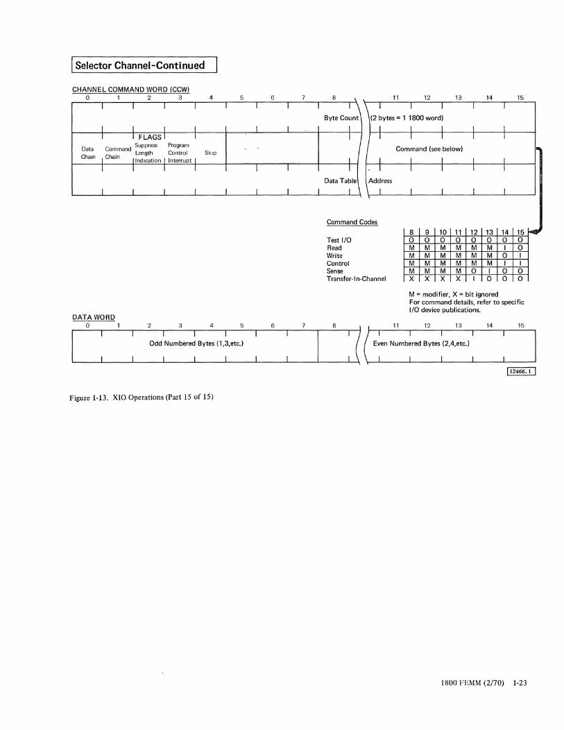
I Selector Channel-Continued
CHANNEL COMMAND WORD (CCW) o 1 3
Data Cham
DATA WORD
Skip
o 2 3 4 5
I : : Figure 1-13. XIO Operations (Part 15 of 15)
6 7
: : I
11 12 13 14 15
\ I I I I I
Byte Count (2 bytes = 1 1800 word)
Data Table
Command C
Test I/O Read
I I
I I
Address
I
odes
Write Control Sense Transfer-In-Channel
8
I I I I I I I I
Command (see below)
I I I I I I I I
I I I I
8 9 10 11 12 13 14 15 0 0 0 0 0 0 0 0 M M M M M M I 0 M M M M M M 0 I M M M M M M I I M M M M 0 I 0 0 X X X X I 0 0 0
M = modifier, X = bit ignored For command details, refer to specific I/O device publications.
15
~
112466.1 1
IRon FEMM (2/70) 1-23
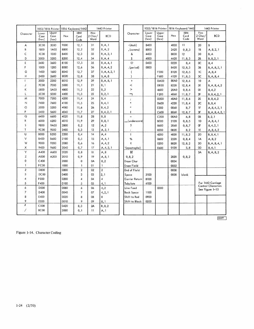
1053/1816 Printer 1 816 Keyboard/1442 1443 Printer 1053/1816 Printer 1816 Keyboard/I442 1443 Printer
Character Lower Upper IBM Hex Case Case Hex Card 2 Char/ BCD (hex) (hex) Code Word
Character lower Upper IBM P.ex Case Case Hex Card 2 Char/ BCD (hex) (hex) Code Word
A 3COO 3EOO 9000 12,1 31 B,A,1 -(dash) 8400 4000 11 20 B
B 1800 lAOO 8800 12,2 32 B,A,2 ,(comma) 8000 2420 0,8,3 lB A,8,2,1
C lCOO lEOO 8400 12,3 33 B,A,2,1 & 4400 8000 12 30 B,A
D 3000 3200 8200 12,4 34 B,A,4 $ 4000 4420 11,8 3 2B B,8 2 1
E 3400 3600 8100 12,5 35 B,A,4,1 @ 0400 0220 8,4 DC 8,4
F 1000 1200 8080 12,6 36 B,A,4,2 . (period) 0000 8420 12,8,3 3B B,A,8,2,1
G 1400 1600 8040 12,7 37 B,A,4,2,1 ( FEOO 8120 12,8,5 lC A,8,4
H 2400 2600 8020 }2,8 38 B,A,8 ) F600 4120 11,8,5 3C B,A,8,4 - -I 2000 2200 8010 12,9 39 B,A,8,1 + DAOO 80AO 12,8,6 10 A
J 7COO 7EOO 5000 11,1 21 B,1 < DEOO 8220 12,8,4 3E B,A,8,4,2
K 5800 5AOO 4800 11 ,2 22 B,2 > 4600 20AO 0,8,6 OE 8,4,2
L 5COO 5EOO 4400 11,3 23 B,2,1 --, F200 4060 11,8,7 2F B,8,4 2,1
M 7000 7200 4200 11,4 24 B,4 ; D200 40AO 11,8,6 2E B,8,4,2
N 7400 7600 4100 11,5 25 B,4,1 * D600 4220 11,8,4 2C B,8,4
0 5000 5200 4080 11,6 26 B,4,2 u E200 0060 8,7 IF A,8,4,2,1
P 5400 5600 4040 11,7 27 B,4,2,1 I C600 8060 12 8 7 3F BA8421
Q 6400 6600 4020 11,8 28 B,8 : C200 OOAO 6,8 OB 8,2,1 R 6000 6200 4010 11,9 29 B,8,1 _(underscore) BEOO 2120 0,8,5 10 A,8,4,1
S 9800 9AOO 2800 0,2 12 A,2 ? 8600 2060 0,8,7 OF 8,4,2,1
T 9COO 9EOO 2400 0,3 13 A,2,1 : 8200 0820 8,2 IE A,8,4,2
U BOOO B200 2200 0,4 14 A,4 ! 4200 4820 11,8,2 2D B,8,4,1
V B400 B600 2100 0,5 15 A,4,1 % 0600 2220 0,8,4 lA A,8,2
W 9000 9200 2080 0,6 16 A,4,2 ~ 0200 8820 12,8,2 3D B,A,8,4,1
X 9400 9600 2040 0,7 17 A,4,2,1 '(apostrophe) E600 0120 5,8 OD 8,4,1
Y MOO A600 2020 0,8 18 A,8 J:( 3A B,A,8,2
Z AOOO A200 2010 0,9 19 A,8,1 0,8,2 2820 0,8,2
0 C400 2000 0 OA 8,2 Erase Char 0004
1 FCOO 1000 1 01 1 Erose Field 0002
2 D800 0800 2 02 2 End of Field 0008
3 DCOO 0400 3 03 2,1 Space 2100 0000 blank
4 FOOO 0200 4 04 4 Carrier Return 8100
5 F400 0100 5 05 4 1 Tabulate 4100 For 1443 Carriage
6 DOOO 0080 6 06 4,2
7 D400 0040 7 07 4,2,1
0300 Control Characters
Line Feed See Figure 1-15 Back Space 1100
8 E400 0020 8 08 8 Shift to Red 0900
9 EOOO 0010 9 09 8 1 Shift to Black 0500 # COOO 0420 8,3 2A B,8,2
/ BCOO 3000 0,1 11 A,1
Figure 1-14. Character Coding
1-24 (2/70)
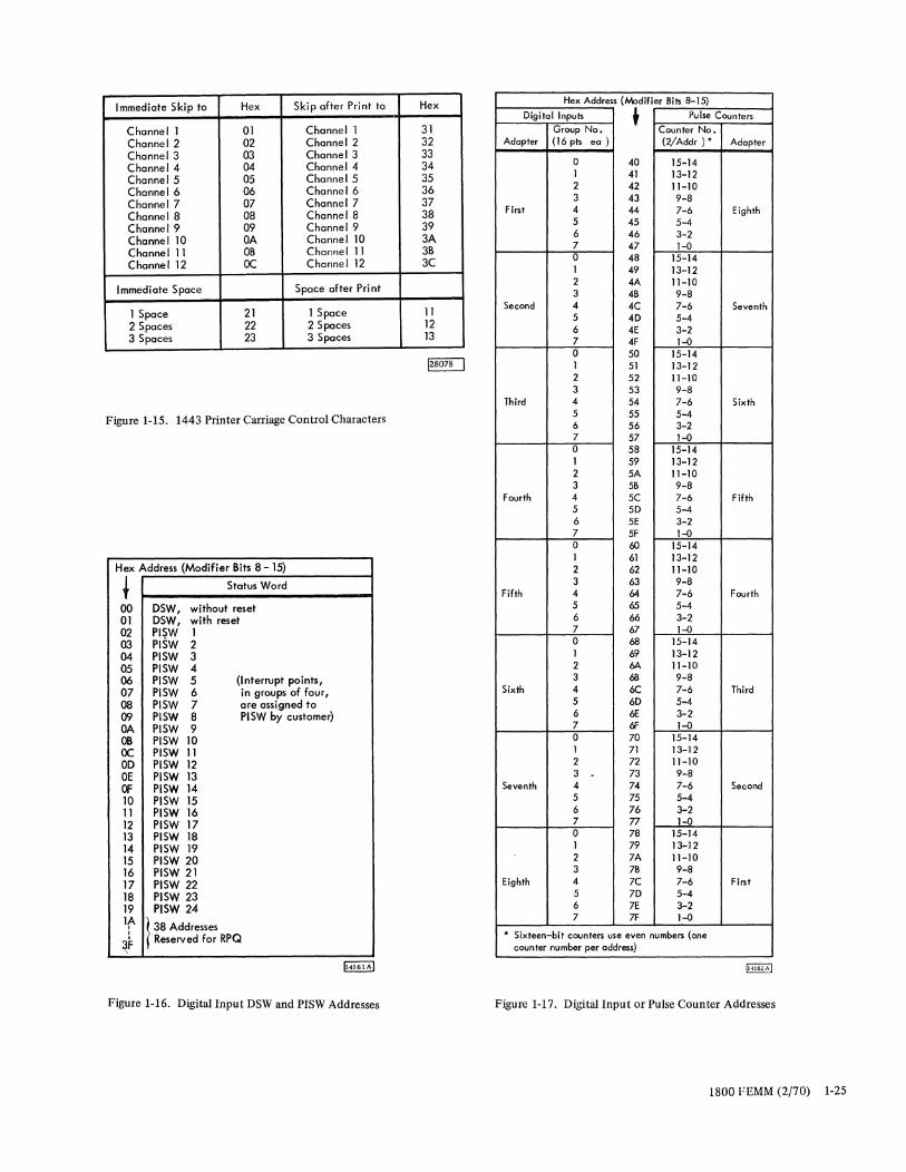
Immediate Skip ta Hex Skip after Print to Hex
Channel I 01 Channel I 31
Hex Address (Modifier 8its 8-15)
Digital Inputs • Pulse Counters Group No. Counter No.
Channel 2 02 Channel 2 32 Adapter (16 pts eo ) (2/Addr ) * Adapter Channel 3 03 Channel 3 33 Channel 4 04 Channel 4 34 Channel 5 05 Channel 5 35 Channel 6 06 Channel 6 36 Channel 7 07 Channel 7 37 Channel 8 08 Channel 8 38 Channel 9 09 Channel 9 39 Channel 10 OA Channel JO 3A Channel I I 08 Channel I I 38
Channel 12 OC Channel 12 3C
0 40 15-14 1 41 13-12 2 42 11-10 3 43 9-8
First 4 44 7-6 Eighth 5 45 5-4 6 46 3-2 7 47 1-0 0 48 15-14 1 49 13-12
Immediate Space Space after Pri nt 2 4A 11-10 3 48 9-8
I Space 21 I Space II 2 Spaces 22 2 Spaces 12 3 Spaces 23 3 Spaces 13
Second 4 4C 7-6 Seventh 5 4D 5-4 6 4E 3-2 7 4F 1-0 0 50 15-14 1 51 13-12 2 52 11-10 3 53 9-8
Third 4 54 7-6 Sixth
Figure 1-15. 1443 Printer Carriage Control Characters 5 55 5-4 6 56 3-2 7 57 1-0 0 58 15-14 1 59 13-12 2 5A 11-10 3 58 9-8
Fourth 4 5C 7-6 Fifth 5 5D 5-4 6 5E 3-2 7 5F 1-0 0 60 15-14 1 61 13-12
Hex Address {Modifier Bits 8 - 15} 2 62 11-10
+ Status Word 3 63 9-8
Fifth 4 64 7-6 Fourth
00 OSW, without reset 01 OSW, with reset 02 PISW I
5 65 5-4 6 66 3-2 7 67 1-0
03 PI5W 2 0 68 15-14
04 PISW 3 1 69 13-12
05 PISW 4 06 PISW 5 (Interrupt points, 07 PISW 6 in groups of four, 08 PISW 7 a re ass i gned to 09 PISW 8 PISW by customer) OA PISW 9
2 6A 11-10 3 68 9-8
Sixth 4 6C 7-6 Third 5 6D 5-4 6 6E 3-2 7 6F 1-0
OB PISW 10 0 70 15-14
OC PISW II 1 71 13-12
00 PISW 12 2 72 11-10
OE PISW 13 3 73 9-8
OF PISW 14 Seventh 4 74 7-6 Second
10 PISW 15 5 75 5-4
II PISW 16 6 76 3-2
12 PISW 17 13 PISW 18
7 77 1-0 0 78 15-14
14 PISW 19 1 79 13-12
15 PISW 20 2 7A 11-10
16 PISW 21 3 78 9-8
17 PISW 22 Eighth 4 7C 7-6 First
18 PISW 23 19 PISW 24
5 7D 5-4 6 7E 3-2
IA } 38 Addresses I
I Reserved for RPQ I
~F
7 7F 1-0
* Sixteen-bit counters use even numbers (one counter number per address)
Figure 1-16. Digital Input DSW and PISW Addresses Figure 1-17. Digital Input or Pulse Counter Addresses
1800 FEMM (2/70) 1-25
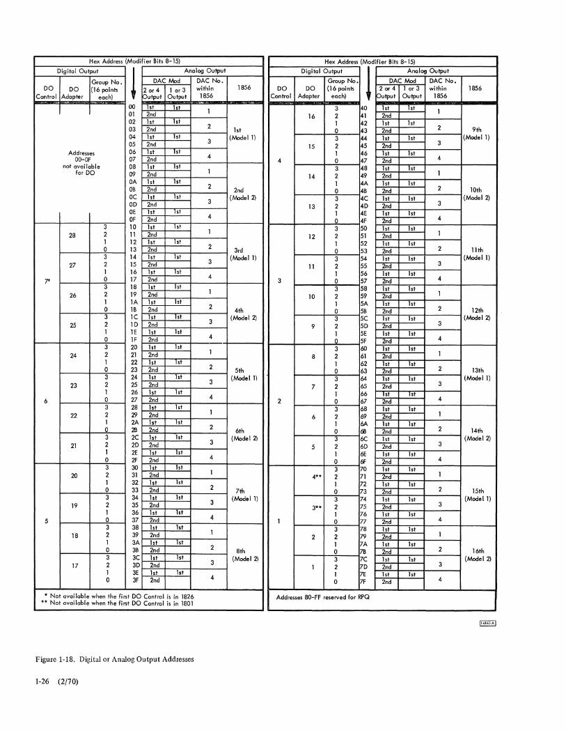
Hex Address (Modifier Bits 8-15) Hex Address (Modifier Bits 8-15)
Digital Output
! Analog Output Digital Output
1 Analog Output
Group No. DAC Mod DAC No. Group No. DAC Mod DAC No. DO DO (16 poin" 2 or 4 1 or 3 within 1856 DO DO (16 poin" 2 or 4 1 or 3 within 1856
Control Adapter each) Output Output 1856 Control Adapter each) Output Output 1856
00 lst lst 1 3 40 lst 1st
1 01 2nd 16 2 41 2nd 02 lst lst 1 42 lst lst 03 2nd 2
lst a 43 2nd 2 9th 04 lst lst (Model 1) 3 44 lst lst (Modell) 05 2nd 3
2 45 2nd 3 15 Addresses 06 lst lst
4 1 46 1st lst OO-OF 07 2nd 4 a 47 2nd 4
not avai labl e 08 lst lst 3 48 1 st lst for DO 09 2nd 1
2 49 2nd 1 14 OA lst lst 1 4A lst lst OB 2nd 2
2nd a 4B 2nd 2 10th OC lst lst (Model 2) 3 4C lst lst (Model 2) aD 2nd 3
2 4D 2nd 3 13 OE 1st st 1 4E 1st lst OF 2nd 4
0 4F 2nd 4 3 10 lst 1st 3 50 1st lst
28 2 11 2nd 1 2 51 2nd 1 12
1 12 lst lst 1 52 1st lst 0 13 2nd 2 3rd a 53 2nd 2 11th 3 14 1st lst (Modell) 3 54 lst lst (Model 1)
27 2 15 2nd 3 2 55 2nd 3 11
1 16 1st lst 1 56 1st lst 0 17 2nd 4
3 a 57 2nd 4 7" 3 18 lst lst 3 58 lst lst
26 2 19 2nd 1 2 59 2nd 1 10
1 lA 1st lst 1 5A lst lst 0 lB 2nd 2
4th a 5B 2nd 2 12th 3 lC 1st lst (Model 2) 3 5C 1st lst (Model 2)
25 2 lD 2nd 3 2 5D 2nd 3 9
1 IE lst 1st 1 5E lst lst a IF 2nd 4
a 5F 2nd 4 3 20 lst 1 st 3 60 lst 1st
24 2 21 2nd 1 8 2 61 2nd 1
1 22 1st st 1 62 lst lst a 23 2nd 2
5th 0 63 2nd 2 13th 3 24 lst lst (Model 1) 3 64 lst 1st (Modell)
23 2 25 2nd 3 2 65 2nd 3 7
1 26 lst lst 1 66 st st 6 0 27 2nd 4
2 a 67 2nd 4 3 28 lst 1 st 3 68 lst lst
22 2 29 2nd 1 2 69 2nd 1 6
1 2A lst lst 1 6A lst lst a 2B 2nd 2
6th a 6B 2nd 2 14th 3 2C lst lst (Model 2) 3 6C 1st lst (Model 2)
21 2 2D 2nd 3 5 2 6D 2nd 3
1 2E lst lst 1 6E lst lst 0 2F 2nd 4
a ~ 2nd 4 3 30 lst lst 3 70 lst 1st
20 2 31 2nd 1 4" 2 71 2nd 1
1 32 lst lst 1 72 lst 1st a 33 2nd 2
7th 0 73 2nd 2 15th 3 34 lst 1st (Modell) 3 74 1st lst (Model 1)
19 2 35 2nd 3 2 75 2nd 3
3·' 1 36 1st lst 1 76 1st lst
5 a 37 2nd 4 1 a 77 2nd 4
3 38 1 st 1st 3 78 1 st lst 18 2 39 2nd 1
2 2 79 2nd 1 1 3A lst 1st 1 7A lst lst a 3B 2nd 2
8th a 7B 2nd 2 16th 3 3C 1 st lst (Madel 2) 3 7C lst lst (Model 2)
17 2 3D 2nd 3 1 2 7D 2nd 3
1 3E 1st lst 1 7E 1 st 1 st 0 3F 2nd 4
a 7F 2nd 4
• Not available when the first DO Control is in 1826 Addresses 80-FF reserved for RPQ •• Not available when the first DO Control is in 1801
Figure 1-18. Digital or Analog Output Addresses
1-26 (2/70)
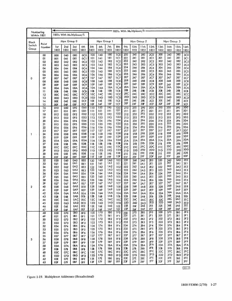
Numbering "II 185ls With Multiplexer/R P
Within 1851 1851s With Multlplexer/S
Block Point Mpx Group 0 Mpx Group I Mpx Group 2 Mpx Group 3
Switch Group Number 1st 2nd 3rd 4th 5th 6th 7th 8th 9th 10th II th 12th 13th 14th 15th 16th
1851 1851 1851 1851 1851 1851 1851 1851 1851 1851 1851 1851 1851 1851 1851 1851
00 000 040 080 OCO 100 140 180 ICO 200 240 280 2CO 300 340 380 3CO 01 001 041 081 OCI 101 141 181 ICI 201 241 281 2CI 301 341 381 3CI 02 002 042 082 OC2 102 142 182 IC2 202 242 282 2C2 302 342 382 3C2 03 003 043 083 OC3 103 143 183 1C3 203 243 283 2C3 303 343 383 3C3 04 004 044 084 OC4 104 144 184 IC4 204 244 284 2C4 304 344 384 3C4 05 005 045 085 OC5 105 145 185 IC5 205 245 285 2C5 305 345 385 3C5 06 006 046 086 OC6 106 146 186 IC6 206 246 286 2C6 306 346 386 3C6
0 07 007 047 087 OC7 107 147 187 IC7 207 247 287 2C7 307 347 387 3C7 08 008 048 088 OC8 108 148 188 IC8 208 248 288 2C8 308 348 388 3C8 09 009 049 089 OC9 109 149 189 IC9 209 249 289 2C9 309 349 389 3C9 10 OOA 04A 08A OCA lOA 14A 18A ICA 20A 24A 28A 2CA 30A 34A 38A 3CA 11 OOB 04B 08B OCB lOB 14B 18B ICB 20B 248 288 2CB 30B 34B 38B 3CB 12 OOC 04C 08C OCC 10C 14C 18C ICC 20C 24C 28C 2CC 30C 34C 38C 3CC 13 000 040 080 OCO 100 140 180 1CO 200 240 280 2CO 300 340 380 3CO 14 OOE 04E 08E OCE 10E 14E 18E ICE 20E 24E 28E 2CE 30E 34E 38E 3CE 15 OOF 04F 08F OCF 10F 14F 18F ICF 20F 24F 28F 2CF 30F 34F 38F 3CF 16 010 050 090 000 110 150 190 IDO 210 250 290 200 310 350 390 300 17 011 051 091 001 III 151 191 IDI 211 251 291 201 311 351 391 301 18 012 052 092 002 112 152 192 ID2 212 252 292 202 312 352 392 302 19 013 053 093 003 113. 153 193 103 213 253 293 203 313 353 393 303 20 014 054 094 004 114 154 194 104 214 254 294 204 314 354 394 304 21 015 055 095 OD5 115 155 195 105 215 255 295 205 315 355 395 305 22 016 056 096 006 116 156 196 106 216 256 296 206 316 356 396 306 23 017 057 097 007 117 157 197 ID7 217 257 297 207 317 357 397 307
I 24 018 058 098 008 118 158 198 ID8 218 258 298 208 318 358 398 308 25 019 059 099 009 119 159 199 109 219 259 299 209 319 359 399 309 26 01A 05A O9A OOA llA 15A 19A lOA 21A 25A 29A 20A 31A 35A 39A 30A 27 OIB 05B O9B OOB lIB 15B 19B lOB 21B 25B 29B 20B 31B 35B 39B 30B 28 01C 05C O9C OOC llC 15C 19C 10C 21C 25C 29C 20C 31C 35C 39C 30C 29 010 05D 090 000 110 15D 190 10D 210 25D 290 20D 310 350 390 300 30 OlE 05E O9E OOE liE 15E 19E 10E 21E 25E 29E 20E 31E 35E 39E 30E 31 OIF 05F O9F OOF IIF 15F 19F 10F 21F 25F 29F 20F 31F 35F 39F 3DF 32 020 060 OAO OEO 120 160 lAO lEO 220 260 2A0 2EO 320 360 3AO 3EO 33 021 061 OAI OEI 121 161 IA1 1 EI 221 261 2AI 2EI 321 361 3Al 3EI 34 022 062 OA2 OE2 122 162 IA2 IE2 222 262 2A2 2E2 322 362 3A2 3E2 35 023 063 OA3 OE3 123 163 IA3 IE3 223 263 2A3 2E3 323 363 3A3 3E3 36 024 064 OM OE4 124 164 IA4 IE4 224 264 2A4 2E4 324 364 3A4 3E4 37 025 065 OA5 OE5 125 165 IA5 1E5 225 265 2A5 2E5 325 365 3A5 3E5 38 026 066 OA6 OE6 126 166 IA6 IE6 226 266 2A6 2E6 326 366 3A6 3E6 39 027 067 OA7 OE7 127 167 IA7 1E7 227 267 2A7 2E7 327 367 3A7 3E7
2 40 028 068 OA8 OE8 128 168 IA8 IE8 228 268 2A8 2E8 328 368 3A8 3E8 41 029 069 OA9 OE9 129 169 1A9 IE9 229 269 2A9 2E9 329 369 3A9 3E9 42 02A 06A OAA OEA 12A 16A IAA lEA 22A 26A 2AA 2EA 32A 36A 3AA 3EA 43 028 068 OAB OEB 12B 168 lAB IEB 22B 268 2AB 2EB 32B 368 3AB 3EB 44 02C 06C OAC OEC 12C 16C lAC IEC 22C 26C 2AC 2EC 32C 36C 3AC 3EC 45 020 060 OAD OEO 120 160 lAO lEO 220 26D 2AO 2EO 320 360 3AO 3ED 46 02E 06E OAE OEE 12E 16E 1AE lEE 22E 26E 2AE 2EE 32E 36E 3AE 3EE 47 02F 061' OAF OEF 12F 16F IAF IEF 22F 261' 2AF 2EF 32F 361' 3AF 3EF 48 030 070 OBO OFO 130 170 1BO 1FO 230 270 2BO 2FO 330 370 3BO 3FO 49 031 071 OBI OFI 131 171 IBI IFI 231 271 2BI 2Fl 331 371 3BI 3F1 50 032 072 OB2 OF2 132 172 IB2 IF2 232 272 2B2 2F2 332 372 3B2 3F2 51 033 073 083 OF3 133 173 IB3 lF3 233 273 2B3 2F3 333 373 3B3 3F3 52 034 074 OB4 OF4 134 174 IB4 lF4 234 274 2B4 2F4 334 374 384 3F4 53 035 075 OB5 OF5 135 175 IB5 lF5 235 275 2B5 2F5 335 375 385 3F5 54 036 076 OB6 OF6 136 176 lB6 IF6 236 276 2B6 2F6 336 376 3B6 3F6 55 037 077 OB7 OF7 137 177 IB7 IF7 237 277 2B7 2F7 337 377 3B7 3F7
3 56 038 078 OB8 OF8 138 178 lB8 IF8 238 278 288 2F8 338 378 3B8 3F8 57 039 079 OB9 OF9 139 179 lB9 IF9 239 279 2B9 2F9 339 379 3B9 3F9 58 03A 07A OBA OFA 13A 17A IBA 1FA 23A 27A 2BA 2FA 33A 37A 3BA 3FA 59 03B 078 OBB OFB 138 178 1BB 1FB 238 27B 2BB 2FB 338 37B 3BB 3FB 60 03C 07C OBC OFC 13C 17C 1BC IFC 23C 27C 2BC 2FC 33C 37C 3BC 3FC 61 030 070 OBO OFO 130 170 1BO IFO 230 270 2BO 2FD 33D 370 3BO 3FD 62 03E OlE OBE OFE 13E 17E IBE lFE 23E 2lE 2BE 2FE 33E 37E 3BE 3FE 63 03F 07F OBF OFF 13F 17F 1BF IFF 23F 27F 2BF 2FF 33F 37F 38F 3FF
Figure 1-19. Multiplexer Addresses (Hexadecimal)
1800 FEMM (2/70) 1-27
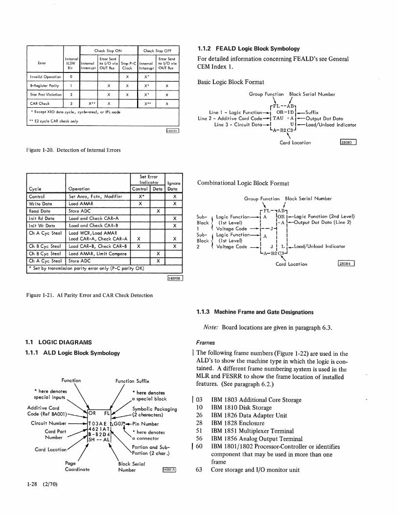
Check Stop ON Check Stop OFF
Internal Error Sent Error Sent Error ILSW Internal to I/O vio Stop P-C Internal to I/O vio
Bit Interrupt OUT Bus Clock Interrupt OUT Bus
Invalid Operation 0 X X'
B-Register Parity 1 X X X' X
Star Prot Violation 2 X X X' X
CAR Check 3 X" X X" X
* Except XIO data cycle, cycle-steal, or IPL mode
** E2 cycle CAR check only
Figure 1-20. Detection of Internal Errors
Set Error Indicator Ignore
Cycle Operation Control Data Data
Control Set Area, Fctn, Modifier X·
Write Data Load AMAR X
Read Data Store ADC X Init Rd Data Load and Check CAR-A
Init Wr Data Load and Check CAR-B
Ch A Cyc Steal Load WCR, Load AMAR Load CAR-A, Check CAR-A X
Ch B Cye Steal Load CAR-B, Check CAR-B X
Ch B Cyc Steal Load AMAR, Limit Compare X
Ch A Cye Steal Store ADC X • Set by transmission parity error only (P-C parity OK)
Figure 1-21. AI Parity Error and CAR Check Detection
1.1 LOGIC DIAGRAMS
1.1.1 ALD Logic Block Symbology
Function Function Suffix
• here denotes special inputs
* here denotes a special block
Additive Card Code (Ref BAOOl)
Circuit Number --.-J~~~~ 1 T~tl.GO~--:in Number
Card Part B _ B 2 0 4 "'" here denotes Number 5H __ AL a connector
Card Location I \ Portion ond SubPortion (2 char.)
Page Block Serial Coordinote Number
1-28 (2/70)
X
X
X
X
X
X
1.1.2 FEALD Logic Block Symbology
For detailed information concerning FEALD's see General CEM Index 1.
Basic Logic Block Format
Group Function Block Serial Number
\ I rFL--AB1
Line 1 - Logic Function_I OR-ID I---Suffix Line 2 - Additive Card Code-I TAU +A I---Output Dot Data
Line 3 - Circuit Data_I U I-Load/Unload Indicator LA-B2C3 J
\ Card Location
Combinational Logic Block Format
Sub- j ~Iock t Sub- { ~Iock
Group Function Block Serial Number
\ I .-FL-"TAB,
Logic Function-I A lOR I-Logic Function (2nd Level) (lst Level) I I+A I-Output Dot Data (Line 2)
Voltage Code -I--J-i I Logic Function---...I A I I
(1 st Level) II I I Voltage Code _I J I L I_Load/Unload Indicator
LA-B2C3...J
"'-Card Locat ion 128084 1
1.1.3 Machine Frame and Gate Designations
Note: Board locations are given in paragraph 6.3.
Frames
I The following frame numbers (Figure 1-22) are used in the ALD's to show the machine type in which the logic is contained. A different frame numbering system is used in the MLR and FESRR to show the frame location of installed features. (See paragraph 6.2.)
03 IBM 1803 Additional Core Storage 10 IBM 1810 Disk Storage 26 IBM 1826 Data Adapter Unit 28 IBM 1828 Enclosure 51 IBM 1851 Multiplexer Terminal 56 IBM 1856 Analog Output Terminal 60 IBM 1801/1802 Processor-Controller or identifies
component that may be used in more than one frame
63 Core storage and I/O monitor unit
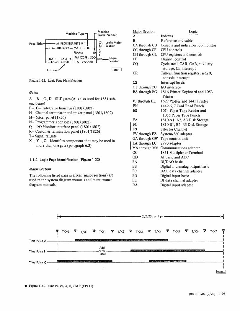
Page Title
Machine ~ ____ M_a_C_h_in_e_T_yp_e} Frame Number
I ~ M REGISTER BITS 0 1 CL} Logic Major l Section E.C.-HISTORY MACH. 1800 7
~FRAME 6O?
DATE LAST EC IBM CORP. SDD 006_ Logi~ 12-17-68 411980 P.N.2279570 VersIon
EC Level / 112467 I
Figure 1-22. Logic Page Identification
Gates
A -, B-, C-, D- SLT gates (A is also used for 1851 subenclosure) F-, G- Integrator housings (1801/1802) H- Channel terminator and mixer panel (1801/1802) M- Mixer panel (1856) N- Programmer's console (1801/1802) Q - I/O Monitor interface panel (1801/1802) R- Customer termination panel (1801/1826) T - Signal tailgate x- y - Z- Identifies component that may be used in
, mo;e than one gate (paragraph 6.3)
1.1.4 Logic Page Identification (Figure 1-22)
Major Section
The following listed page prefixes (major sections) are used in the system diagram manuals and maintenance diagram manuals.
Major Section A-B-CA through CB CC through CF CH through CL CP CQ
CR
CS CT through CU EA through EG
Indexes Reference and cable Console and indicators, op monitor CPU controls CPU registers and controls Channel control Cycle steal, CAR, CAB, auxiliary
storage, CE interrupt Timers, function register, area 0,
console interrupt Interrupt levels I/O interface 1816 Printer Keyboard and 1053 Printer
EJ through EL 1627 Plotter and 1443 Printer EN 1442-6,7 Card Read Punch ES 1054 Paper Tape Reader and
1055 Paper Tape Punch FA 181O-Al,A2,A3DiskStorage
I FC 181O-Bl, B2, B3 Disk Storage FS Selector Channel FV through FZ System/360 adapter GA through GW Tape control unit
I LA through LC 2790 adapter MA through MM Communications adapter QC 1851 Multiplexer Terminal QD AI basic and ADC P A DI/DAO basic PB Digital and analog output basic PC DAO data channel adapter PD Digital input basic PE DI data channel adapter RA Digital input adapter
1..1411------------------2,2.25, or 4jJs -------------'t>-\
T T/XO V T/Xl '" T/X! V T/X2 VI T/X3 V T/X4 'f' T/X5 ViI T/X6 VI T/X7 r _-lI ____ ~ ...................... t.MWWma ______________ ~1 Ai , .. _ Time Pulse A I I
I I __ ~II--------___ !tt ______ ~ee .... W.;;~M .. iiB.RE .. 53*H&* ...... *Mgm-mi@~,~am~WM~mw~-----1:
Time Pulse B i 1803 I
Time Pulse C __ J1 ________ •••• IIL ________ .lilllFil'llltW.WIlllllAA-.4mm*m':IIi!:IIi!!!l!S"~g:!l!WMBL-------_l!
12B091A I
• Figure 1-23. Time Pulses, A, B, and C (CPlll)
1800 FEMM (2/70) 1-29
Major Section
RB RC SA and SD TA TL WA
Iwx WZ XA YA YB YC YF YS
Logic
Pulse counter adapter Process interrupt adapter Core storage 1856 analog output terminal Digital output adapter I/O monitor 1803 Core Storage Unit Core storage interface Single disk storage 1801/1802 power control 1826 power control 1810 power control DC power supplies 1803 power control
With the exception of second-order products, such as core storage and single disk storage, only one set of logics is provided for multiple features within a machine type. For example, if the 1826 and the 1801 each contain two digital input adapters, two sets of RA logics will be sent with the system -- one for the 1826 and one for the 180l. Likewise, if a feature is not included in the machine type, no set of logics will be provided for that feature.
Version
The logic version number appears in the lower corner of the logic page. Logic version numbers 000-049 are reserved for basic system and basic system features. Non RPQ logic versions and associated applications are:
000 - Basic system 004 - Installed once with any of the following features:
selector channel, communications adapter, 1800/ 2790 adapter, expanded core storage, expanded data channels
005 - Installed with core storage expansion beyond 32k (1803 attached)
006 - Installed with data channel expander (more than nine data channels)
The highest numbered version of logic always takes precedence according to the features installed on the system.
Note: Version numbers above 050 apply to RPQ's. Version numbers below 050 are used here to identify installed features. When RPQ's are incorporated in a system, ALD's are printed on green paper with a version number. Version priority is not related to the version number but is called out in the RPQ installation instructions.
1-30 (2/70)
RPQ Logic Pages
RPQ logic pages are printed on green paper. When an RPQ modifies the information on an existing logic page, the green RPQ logic page will be inserted with the existing page.
1.1.5 System Paperwork Binder
A system paperwork binder is included as part of the maintenance package provided with the 1800 system. The binder contains miscellaneous records and copies of listings pertaining to the individual system. Among these documents are:
1. Quality Assurance Shipping Check List 2. Final Test Shipping Check List (cables) 3. Machine History (hard card) 4. Machine Level Control (MLC) for core storage 5. Cable Order Form 6. Customer Assignment Form (CAF) 7. Summary of Order for System 8. Machine Location Report (MLR) 9. Additional CAF and MLR information for installed
RPQ's 10. Field Engineering Systems Reference Report (FESRR) 11. Manufacturing Assembly Report (MAR-2)
The FESRR is a machine listing of all installed features, except RPQ features, showing board and terminal locations, IOCC addresses, and interrupt and data channel assignments. The MAR-2 forms are generated at the factory to identify all unique customer wiring. Both the FESRR and the MAR-2 must be updated by the customer engineer each time a wiring assignment is changed in the field. (See paragraph 1.2.)
1.2 MANUALLY CONTROLLED WIRING CHANGES
Manually controlled (special purpose) wiring is used in certain areas of the 1800 system to provide the flexibility required for customer assignments, options, and additive features: Manually controlled wiring relates to the unique wire connections that adapt the system to the specific needs of the customer or features. That wiring which is assignable by the customer is also referred to as "personality wiring."
Manual wiring connections, both special purpose and personality, are made with violet wire on the probe side of SLT boards or special mixer panels, using pin-to-pin wrapped terminations.
After the system is shipped, all changes and additions to manual wiring are controlled by the customer engineer.

0 1 2 3 4 5 6 7 8 9 10 11 12 13 14 15
Sign 213 212 211 210 29 28 27 26 25 24 23 l 21 20
Over-load
1 st Hex Character nd 2 Hex Character rd
3 Hex Character 4th Hex Character
Voltage Voltage Voltage Voltage
0 0.0000 0 0.0000 0 0.0000 0 0.0000
1 0.6250 1 0.0391 1 0.0024 1 0 2 1.2500 2 0.0781 2 0.0049 2 0.0003
3 1.8750 3 0.1172 3 0.0073 3 (3)
4 2.5000 4 0.1563 4 0.0098 4 0.0006
5 3.1250 5 0.1954 5 0.0122 5 0 6 3.7500 6 0.2344 6 0.0147 6 0.0009
7 4.3750 7 0.2735 7 0;0171 7 (3)
8 CD 8 0.3125 8 0.0195 8 0.0012
9 CD 9 0.3516 9 0.0219 9 (3)
A CD A 0.3906 A 0.0244 A 0.0015
B CD B 0.4297 B 0.0268 B ® C CD C 0.4688 C 0.0293 C 0.0018
D CD D 0.5079 D 0.0317 D ® E CD E 0.5469 E 0.0342 E 0.0021
F CD F 0.5860 F 0.0366 F ®
Obtain voltage value for each hex character. Sum of four voltage values equals ADC voltage reading. For low-level inputs, reading must be corrected to compensate for differential amplifier gain.
Negative reading. Obtain two's complement (subtract hex reading from /FFFF and add 1) of ADC value and obtain equivalent positive value from chart.
Figure 1-24. ADC Register Voltage Values
o Overload bit is on. ADC value is meaningless.
1800 FEMM (2/70) 1-31
It is the CE's responsibility to update the system records after each change and to edit the diagnostic program decks as necessary.
For additional information on wiring changes, see 1800 Service Aid number 29.
1.2.1 Authorization for Wiring Changes
Customer assigned wiring can be changed by the CE at the customer's request when authorized by the FE branch manager. Other types of manually controlled wiring may be changed when authorized by an MES, RPQ, or engineering change. No altering of customer assignments will result from an engineering change. If an engineering change affects a net containing customer-assigned wiring, the field instructions will specify the action required to maintain the present assignments.
MES and RPQ Orders
These orders usually specify installation or removal of additive or special features and may necessitate rework of existing manual wiring, including customer assigned wiring.
The order will include a new Machine Location Report (MLR) and instructions for accomplishing manual wiring other than customer-assigned wiring. If additional installation information is required, an 1800 MES ReqUirements form will be supplied. (See 1800 Service Aid number 18.)
If the rework affects customer-assigned wiring, the CE must obtain the new assignments from the customer (see "Customer Request").
Types of feature wiring controlled by MES order include:
Pulse counter 8-bit or 16-bit option DI (voltage) high-speed option AO optional features IPL wiring for first 1442 (or 1054 ifno 1442) Additive features (interrupts, data channels, I/O adapters,
process I/O groups, etc.) Communications adapter code (EBCDIC or USASCIl)
and data set clocking
Customer Request
Changes to customer-assigned wiring can be made at the customer's request without the need for an MES order. This provision results in minimum turnaround time for the change. The customer must submit a written request to the FE branch manager, who authorizes the CE to make the change. This request must be filed with the system records.
The following manual wiring assignments are controlled by customer request:
Data channel assignment Interval timer bases Interrupt level assignment
1-32 (2/70)
ILSW bit assignment PISW bit assignment System/360 adapter address and select-bypass Communications adapter wiring to match customer's
data sets
Assignments of interrupt level, ILSW bit, and PISW bit are indicated on the Customer Assignment Form provided with the system. Interval timer bases and data channel assignments are indicated in the MLR by 9xxx "specify" codes. The 9xxx codes associated with interval timers and data channel assignments are unique because they are not under machine level control and, therefore, do not require an MES order for authorization to change.
1.2.2 Data Channel Assignment
Initial assignment of an I/O device to a data channel is designated by the 9xxx specify code which is recorded on the MLR. Each device that can operate on a data channel has fifteen unique specify codes corresponding to the fifteen data channels.
Reassignment of a device to a data channel must be authorized by MES, RPQ, or customer request with FE branch manager approval.
Wiring Procedure
1. Determine present wiring assignments and make a wire delete list using CU992 and CU993, if marked, or the FESRR and MAR-2 listing. Compare this list against actual system wiring.
2. Make a list of the new cycle-steal assignments, by device, and compare assignments with the order given on BC 101. If the new assignments accompany a feature installation, verify with the customer that the 9xxx specify codes listed in the new MLR are correct.
3. Using CT990 and the list of new assignments as a reference, assign the adapters to a CS request line (A-Q) on CU992 by writing the adapter name above the line to which it is assigned. Use existing assignments as much as possible. Erase any existing marks and write new assignments in pencil.
4. On CU992, draw in pencil the new level assignments. For example, if the 1443 is on line F and is to be assigned to level 6, draw a line from D-AIN7B05 to D-AIM4B05.
5. Hand mark CU993 to exactly agree with CU992. Pin numbers will vary, but the lines, mixing, and priority assignments must agree. When properly maintained, CU992 and CU993 reflect the data channel wiring of the system and can be used to develop a delete list for future changes in customer assignments.
6. Prepare new edit cards (or paper tape) for diagnostic monitor and diagnostic function tests as required. Refer to paragraph 1.2.7.
7. Perform wiring as drawn on CU992 and CU993, using violet wire (p /N 811696) only.
8. Run diagnostic tests with the new edit cards (or paper tape) to verify proper assignment and editing. Update disk maintenance library (DIMAL) if applicable.
9. Notify the customer that wiring has been completed and have the customer run test case with the new assignments.
10. Update FESRR and the applicable MAR-2 pages. 11. Use service code 31 to cover elapsed time.
1.2.3 Timer Interval Reassignment
Initial assignment of interval timer bases is designated by the 9xxx specify code which is recorded on the MLR. Reassignment of a time base can be authorized by MES or by customer request via the FE branch manager.
Wiring Procedure
1. Refer to system diagram BC150 and convert the 9xxx interval timer feature code to the corresponding time base, using Table E.
2. Develop delete list, using the MAR-'-2 wire list as a reference.
3. Develop add list by referring to Table A on BC150. The MAR-2 wire list, when updated, can serve as the add/delete list.
4. Prepare new edit cards (or paper tape) for diagnostic monitor and diagnostic function tests as required. Refer to paragraph 1.2.7.
5. Perform add/delete wiring. (Use only violet wire, PIN 811696.)
6. Run diagnostic tests with the new edit cards (or paper tape) to verify proper assignment and editing. Update disk maintenance library (DIMAL) if applicable.
7. Notify customer that wiring has been completed and have customer run test case with the new assignments.
8. Update FESRR and the MAR-2 page. 9. Use service code 31 to cover elapsed time.
1.2.4 Interrupt Assignments
Initial assignment of interrupt levels, ILSW bits, and PISW bits is indkated on the Customer Assignment Form.
After the system is shipped, all changes and additions to interrupt assignments (including those made in conjunction with a sales MES or RPQ) must be authorized by customer request approved by the FE Branch Manager.
Wiring Procedure -- System Interrupts
1. List the new interrupt levels and ILSW bit assignments per device.
2. Select the appropriate diagrams from the folloWing table:
Logic Poge Device Reference
Console and Timers BC 150 CU991
1053/1816 EAOOI EA 991
1054/1055 ES 001 ES 992
1442 ENOOI EN991
1443 EJ 005 EJ 991
1627 EJ 001 EJ 991
1810 FA 001 FA991
S/360 Adapter FVOOI FZ991
TCU (1802 only) GAlli GB991
Analog Input QD041 QD99 I
Dig & Anlg Output PB 000 PA991
Digital Input PDOOO PA991
Selector Channel FSOII FSOl3
Communications Adapter MA008 MB997
3. Refer to the MAR-2 sheets and the wiring tables on the referenced diagrams and develop add/delete lists for the following assignments in each adapter affected:
Interrupt level assignment ILSW bit assignment Sense ILSW decode Poll interrupt level
The MAR-2 wire lists, when updated, can serve as the add/delete list.
4. Prepare new edit cards (or paper tape) for diagnostic monitor and diagnostic function tests as required. Refer to paragraph 1.2.7.
5. Perform add/delete wiring. (Use only violet wire, PIN 811696.)
6. Run diagnostic tests with the new edit cards (or paper tape) to verify proper assignment and editing. Update disk maintenance library (DIMAL) if applicable.
7. Notify customer that wiring has been completed and have customer run test case with the new assignments.
8. Update FESRR, Customer Assignment Form, and the applicable MAR - 2 sheets.
9. Use service code 31 to cover elapsed time.
Wiring Procedure -- Process Interrupts
1. List the new interrupt levels, ILSW bit assignments, and PISW bit assignments for each board group.
Note: Three 16-bit PI (contact or voltage) groups may be installed in the adapter. Process interrupts in each PI group are divided into four "board groups" of four bits. These board groups are numbered lA, IB, IC, !D, 2A ... through 3D. Each board group can be
1800 FEMM (2/70) 1-33
2.
3.
assigned to a unique interrupt level; however, the selected level must be within the range specified for the adapter -- either 0 through 11 or 12 through 23.
Refer to Note 1 on system diagram RC841 and determine the appropriate cable plugging for the desired interrupt range of the adapter. Refer to the MAR-2 sheets and the wiring tables on the system diagrams given in the following list. Develop add/delete lists for the wiring assignments in each board group. Observe all notes on these pages. The MAR-2 wire lists, when updated, can serve as the add/delete lists.
Logic Page Board Group Reference
I nterrupt Level RCOOI i RC99 1* Sense ILSW/PISW RCOO2 I RC971* ILSW Bits RCOO4 I RC981*
* On current production, MAR-2 sheets are located in the System Paperwork Binder.
4. Prepare new edit cards (or paper tape) for diagnostic function tests as required. Refer to paragraph 1.2.7.
5. Perform add/delete wiring. (Use only violet wire, PIN 811696.)
6. Run diagnostic tests with the new edit cards (or paper ~ape) to verify proper assignment and editing. Update disk maintenance library (DIMAL) if applicable.
7. Notify customer that wiring has been completed and have customer run test case with the new assignments.
8. Update FESRR, Customer Assignment Form and MAR - 2 sheets.
9. Use service code 31 to cover elapsed time.
1.2.5 System/360 Adapter Address Reassignment
The System/360 channel address of the System/360 adapter can be reassigned at the customer's request or as the result of an MES or RPQ order. Select-bypass jumpering for the adapter can also be reassigned by MES, RPQ, or customer request.
Wiring Procedure
1. Refer to the following system diagrams and determine the necessary jumper changes by comparing new assignments with present jumpering of the addressselect/generate card and the select-bypass card.
1-34 (2/70)
System/360 Adapter Logic Page Reference
Address Select & Generate FVOO5 I FY10l Select In/Out Bypass FVOO5 I FV25 1
2. Change placement of program caps on the cards to conform to new assignments.
3. Prepare new edit cards for System/360 diagnostics as required.
4. Run diagnostic tests (System/360) with the new
5.
6.
edit cards to verify proper assignment and editing. Notify customer that wiring has been completed and have customer run test case with the new assignments. Indicate new assignments on the affected system diagrams.
7. Use service code 31 to cover elapsed time.
Diagnostic PID Features
Monitor OB01 All Disk Maintenance Library Initial Loader OBB7 1B10A Meter Exerciser OBB6 1442
1443 1B10 2400
1053/1B16 Function Test 0806 1053/1B16 2400 Function Test 0807 2400 2400 Timing Test 08B9 2400 2400 I nterchange and Skew Test 080B 2400 2400 Cyclic Redundancy Check OBBD 2400 1054/1055 Function Test OB04 1054
1055 1627 Function Test 0805 1627 2315 Initialization 080B 1B10A 1B10 Function Test OB09 lBl0A 1443 Function Test OBCA 1443 1442 Function Test 080F 1442 AI Dllta Channel (Random) Function Test 0821 AI, Interval Timers AI Data Channel (Sequential) Function Test 0822 AI, Interval Timers AI Direct Program Control Function Test 0823 AI, Interval Timers 01 Data Channel Function Test OB24 01 01 Direct Program Control Function Test OB25 01
PI AO Function Test 0826 AO DO Function Test 0827 DO System/360 Adapter - Section 1 OB2B S/360 Adapter System/360 Adapter -Section 2 OB29 S/360 Adapter Selector Channel Function Test OB10 Selector Channel 2B41 Function Test OB11 Selector Channel 2311 Function Test OB12 Selector Channel 2841 Two-Channel Switch Function Test OB13 Selector Channel 2311 CE Pack Initial ization OB14 Selector Channel 2B41/2311 MPX On-Line Test OB92 Selector Channel Comm Adapt Transmit-Receive OBOD Comm Adapt Comm Adapt Wrap Around 080E Comm Adapt Comm Adapt MPX On-Line Test OB91 Comm Adapt 2790 Adapter OB2B 2790
OB2C 2790 OB2D 2790
1.2.6 Communications Adapter and Line Adapter
Wiring assignments on the communications adapter (CA) and line adapter (LA) boards are determined by the data sets to
be used, the line type, and the desires of the customer. Reassignment of manual wiring can be authorized by MES or by customer request via the FE branch manager.
The CA and LA require personality wiring in addition to the usual data channel and interrupt assignments. See MA20151 for the purposes of all wired logic lines.
Wiring Procedure
1. Refer to system diagrams MA008, MK008, MB997, MB998, and MB999. Using the wiring tables on these diagrams, together with the MAR-2list, develop add/ delete list. The MAR-2 list, when updated, can serve as the add/delete list.
2. Prepare new edit cards (or paper tape) for diagnostic monitor and diagnostic function tests as required. Refer to paragraph 1.2.7.
3. Perform add/delete wiring. (Use only violet wire, PIN 811696.)
4. Run diagnostic tests with the new edit cards (or paper tape) to verify proper assignment and editing. Update disk maintenance library (DIMAL) if applicable.
5. Notify customer that wiring has been completed and have customer run test case with the new assignments.
6. Update FESRR and the MAR-2 sheet. 7. Use service code 31 to cover elapsed time.
1.2.7 Editing Diagnostic Programs
The editing procedure for each diagnostic program is outlined in the maintenance diagnostic programs manual. The first page of volume 1 of the maintenance diagnostic programs lists the volume in which the description for a program is located. Paragraph 6.1 of each deSCription details the edit procedure.
The above table lists diagnostics and indicates which feature wiring will affect them.
Section 2. Diagnostic Techniques
1.3 ON-LINE SERVICING LIMITATIONS
Several maintenance features of the 1800 system are designed specifically to permit diagnosis and servicing while the customer program is operating from main storage. However, the customer must be notified prior to performing anyon-line maintenance that might affect the process control operation, either directly (via an output device) or indirectly (via the operating program).
Limitations and precautions that should be observed during the on-line maintenance activity are defined in the follOWing paragraphs.
Note: Operating limitations for the MPX On-Line Diagnostics are described in 1800 Service Aid 138 and in the 1800 Multiprogramming Executive Opera-ting System Programmers Guide, Order No. GC26-3720.
1.3.1 Use of Auxiliary Storage
If the auxiliary storage program is destroyed, it is possible for the system to become locked in auxiliary storage. Therefore, the customer should be notified when the CE intends to use auxiliary storage, so that restart procedures can be planned in advance.
The customer option to place two devices on the same data channel imposes limitations on shared-time servicing. When one of these devices is to be serviced on-line from auxiliary storage, it will be necessary to take both devices from the customer and place the second device in a "not ready" condition by some manual means, such as removing power to the device.
If the 1442 shares a data channel with another device, both devices will have to be taken if it is necessary to load an auxiliary program.
See 2.6 for a more detailed explanation of auxiliary storage.
Care should be taken to ensure that any device to be serviced on line from auxiliary storage will not be needed by the operating system, causing the customer's program to hang up. The procedures that must be followed to allow the TSX operating system to select alternate devices are explained in "IBM 1800 TSX System Maintenance" of IBM 1800 Time-Sharing Executive Operating Pro-cedures, Order No. GC26-3754.
1.3.2 Power Removal and Component Plugging
Power cannot be turned on or off at any 1800 system unit without the possibility of system interference.
On-line servicing that requires removal of power from any system unit, or removal and replacement of cables or pluggable components within these units, is not recommended if the customer has no reset-and-restart procedure. Even with the P-C stopped and placed in SI, SSC, load, or display mode (to prevent cycle stealing), there is still a possibility of upsetting the status of latches and flip-flops with transients created by interrupting electrical circuits.
To safely remove power from any 1800 system unit, I without System/360 adapter (See 1.3.4), proceed as follows:
1. Power down the system. 2. Observe proper channel termination. (See 1.3.3) 3. Remove cables or power from system unit to be taken
offline. 4. Restore power to system.
To return a system unit to on-line operation, follow the same procedure except that the unit is added rather than removed.
1800 FEMM (2/70) 1-35
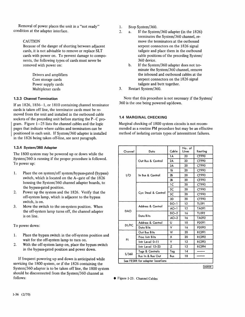
Removal of power places the unit in a "not ready" condition at the adapter interface.
CAUTION Because of the danger of shorting between adjacent cards, it is not advisable to remove or replace SLT cards with power on. To prevent damage to components, the following types of cards must never be removed with power on:
Drivers and amplifiers Core storage cards Power supply cards Multiplexer cards
1.3.3 Channel Termination
If an 1826, 1856-1, or 1810 containing channel terminator cards is taken off line, the terminator cards must be removed from the unit and installed in the outbound cable sockets of the preceding unit before starting the P-C program. Figure 1-25 lists the channel cables and the logic pages that indicate where cables and terminators can be positioned in each unit. If System/360 adapter is installed in the 1826 being taken off-line, see next paragraph.
1.3.4 System/360 Adapter
The 1800 system may be powered up or down while the System/360 is running if the proper procedure is followed. To power up:
1. Place the on system/off system/bypass-gated (bypass) switch, which is located on the A-gate of the 1826 housing the System/360 channel adapter boards, to the bypass-gated position.
2. Power up the system and the 1826. Verify that the off-system lamp, which is adjacent to the bypass switch, is on.
3. Move the switch to the on-system position. When the off-system lamp turns off, the channel adapter is on line.
To power down:
1. Place the bypass switch in the off-system position and wait for the off-system lamp to turn on.
2. With the off-system lamp on, place the bypass switch in the bypass-gated position and power down.
If frequent powering up and down is anticipated while servicing the 1800 system, or if the 1826 containing the System/360 adapter is to be taken off line, the 1800 system should be disconnected from the System/360 channel as
1. 2.
3.
Stop System/360. a. If the System/360 adapter (in the 1826)
terminates the System/360 channel, remove the terminators at the outbound serpent connectors on the 1826 signal tailgate and place them in the outbound cable positions of the preceding System/ 360 device.
b. If the System/360 adapter does not terminate the System/360 channel, remove the inbound and outbound cables at the serpent connectors on the 1826 signal tailgate and butt together.
Restart System/360.
Note that this procedure is not necessary if the System/ 360 is the one being powered up/down.
1.4 MARGINAL CHECKING
Marginal checking of 1800 system circuits is not recommended as a routine PM procedure but may be an effective method of isolating certain types of intermittent failures.
No. of Channel Data Cable Lines Routing
lA 20 CT990
Out Bus & Control 2A 20 CT990
3A 20 CT990
lB 20 CT990
I/o In Bus & Control 2B 20 CT990
3B 20 CT990
lC 20 CT990
2C 20 CT990 Cye Steal & Control 3C 20 CT990
3D 20 CT990
DO-l 12 TL091 Address & Control
AO-l 12 TA091 DAO
DO-2 16 TL092 Data Bits
AO-2 16 TA092
Address & Control U 10 PD091 DI/PC
Data Bits V 16 PD095
Out Bus Bits W 20 RC091
Proe Intr Bits X 20 RC092 PI
Intr Level 0-11 Y 12 RC093
Intr Level 12-23 Z 12 RC094
Tags & Controls Tag 14 --S/360
Bus In & Bus Out Bus 18 --See FESRR for adapter locations
follows: • Figure 1-25. Channel Cables
1-36 (2/70)
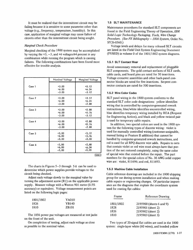
It must be realized that the intermittent circuit may be failing because it is sensitive to some parameter other than voltage (e.g., frequency, temperature, humidity). In this case, application of marginal voltage may cause failure of circuits other than the intermittent circuit being sought.
Marginal Check Procedure
Marginal checking of the 1800 system may be accomplished by varying the +3, -3, and +6 voltages±4 percent in any combination while running the program which is causing failures. The following combinations have been found most effective for trouble analysis.
Nominal Voltage Marginal Voltage
Case 1 +3.00 +3.12 +6.00 +6.24 -3.00 -3.12
Case 2 +3.00 +3.12 +6.00 +6.24 -3.00 -2.88
Case 3 +3.00 +2.88 +6.00 +5.76 -3.00 -3.12
Case 4 +3.00 +2.88 +6.00 +5.76 -3.00 -2.88
Case 5 +3.00 +3.12 +6.00 +5.76 -3.00 -3.00
Case 6 +3.00 +2.88 +6.00 +6.24 -3.00 -3.00
The charts in Figures 5-3 through 5-8 can be used to determine which power supplies provide voltages to the circuit being checked.
Adjust each voltage slowly to the marginal value by turning the adjustment screw (Rl) on the applicable power supply. Measure voltage with a Weston 901 meter (0.5% accuracy) or equivalent. Voltage measurement points are listed on the following logic pages:
1801/1802 1826 1810
YAOlO YB140 ZB101
The 1856 power pac voltages are measured at test jacks on the front of the unit.
On completion of testing, adjust each voltage as close as possible to the nominal value.
1.5 SL T MAINTENANCE
Maintenance procedures for standard SLT components are found in the Field Engineering Theory of Operation, IBM Solid Logic Technology Packaging, Tools, Wire Change Procedure. (See FE Bibliography --1800 System, Order No. SY26-0560.)
Voltage levels and delays for many released SLT circuits are listed in the Field Unit System Engineering Document (FUSED) in volume 0 of the 1801/1802 system diagrams.
1.5.1 SL T Contact Wear
Avoid unnecessary removal and replacement of pluggable SLT components. The gold contact surfaces of SLT cards, cable cards, and board pins are rated for 50 insertions. Voltage crossover assemblies and other back-panel connector blocks are rated for five insertions. Serpent connector contacts are rated for 500 insertions.
1.5.2 Wire Color Codes
SLT panel wiring in the 1800 system conforms to the standard SLT color code designations: yellow identifies wiring that is controlled by computer-generated rework instructions, blue/white identifies uncontrolled wiring, blue identifies temporary wiring installed by REA (Request for Engineering Action), and black and yellow twisted pair is used for temporary cable repairs.
In addition, two special colors are used in the 1800 system for the following types of discrete wiring: violet is used for manually controlled wiring (customer-assignable, manual listing or Feature II addition) that cannot be handled by computer-generated rework instructions, and red is used for all RPQ discrete wire adds. Repairs to nets that contain violet or red wire must always have that portion of the net restored completely, using the same color of special wire that existed before the repair. The part numbers for the special colors of No. 30 A WG solid copper wire are: violet, 811696; and red, 811693.
1.5.3 Machine Cable Installation
Cable reference drawings are included in the 1800 shipping group for use during system installation and when making cable repairs or engineering changes. Of particular importance are the diagrams that explain the coordinate system used for routing flilt cables:
Frame
1801/1802 1828 1826 1810
Reference Drawing
2195900 (sheets 6 and 9) 2195901 (sheet 2) 2195902 (sheet 2) 219 5903 (sheet 3)
Two types of 20-signal flat cables are used in the 1800 system: single-layer white (60 wires), and bonded yellow
1800 FEMM (2/70) 1-37
(20 wires). The white cables may be pre creased at each fold and marked with a transverse line at each clamp position. Bonded cables are unmarked and are not precreased.
Cables that are marked at the fold position should be folded so that the mark is inside the fold.
Note: The 33 A WG solid copper conductors in white flat cable can be broken by repeated folding and unfolding of the cable. Yellow bonded cables contain 22 A WG stranded wire that is not as susceptible to breakage.
The installation instructions shipped with field bills of material direct the routing of flat cables as per the following example: C-B1A6 via B1S2, B2B2, A2B2, A1V2, C1C7 (loop 10 inches), P1R7, P1F7, SlF7, SlA7, S4A3, S4B6 to power tailgate connector. In this example, C-B1A6 identifies the "from" location as gate C, board B 1, connector A6. The "via" locations specify the locations of folds or clamps. The routing of this particular cable is illustrated in Figure 1-26.
The SLT Flat Cable List which is shipped with white flat cables designated fold and clamp positions at each "via" location by channel (CH) and node (ND). Thus, the "via" location B1S2 would be shown as channel B1, node S2. Each ''via'' location on the cable list also specifies the length of cable, in hundredths of an inch, from the last "via" location to the present one, and specifies the fold type (FT). Fold types are shown in Figure 1-27.
The cable list P/N appearing on the "from" label of each flat cable identifies the cable group to which the cable belongs. The sequence number on the "from" and "to" labels identifies the installation sequence of each cable in the group.
Cable retainers, X-type and straight-type, are supplied in the basic machine shipping group and should be used when installing additional cable groups.
There are occasions when random length white cables are sent to the field. The cable list information must be used to install these cables. Random length cables may be longer than necessary, but will never be shorter. Random length cables are identified by a marking near the cable label, indicating the excess length. For example, a marking of +4 indicates an excess length of 4 inches. The excess length must be taken up at loop positions or by folding back in the channel. Random length cables do not have fold or clamp marks but may be precreased. The precreasing on these cables is to be ignored.
If the "to" end of a cable must be twisted 1800 for proper alignment of the connector, this can be accomplished by changing the fold at the last node from type A/B to type D/E or vice-versa. If a cable must be repositioned at the exit point of the channel this can be accomplished at the last fold as shown in Figure 1-28.
1-38 (2/70)
1.6 CRITICAL CIRCUITS AND LEVELS
1.6.1 Sample Pulse Drivers (SPD's)
Proper operation of circuits using gated SPD's as inputs requires that the SPD's have proper turn-on transition time and proper voltage shift. The typical transition time for the + 3V to OV shift is 10 to 20 nanoseconds. If the transition time is greater than 30 nanoseconds, intermittent failures may result. The magnitude of the voltage shift is also critical and should be in the range of 2.8 to 3.3 volts when the particular SPD is used as a gated input. A lesser amount of shift can cause failures to set or reset a multiinput trigger (flip-flop) or to fire an SPD. Greater shift magnitudes can erroneously set or reset a gated trigger when the gate it not conditioned or erroneously fire a gated SPD when the gate is not conditioned.
Because of differences in ac input impedances, a pulse with a fast transition and proper shift is required to fire a gated input SPD, while a slower pulse with less shift will set a multi-input trigger. Therefore, the most common failures are erroneous setting of multi-input triggers and failure to fire gated SPD's.
When scoping SPD's, to check for transition time and shift magnitude, it is essential to use a probe with the shield grounded at the tip.
Defective SPD's can sometimes be detected by marginal checking. (See 1.4 cases 5 and 6.) Figure 1-29 shows SPD waveforms.
1.6.2 Singleshots (SS)
Singleshots of the 1800 system may be positively triggered by jumpering the '-DC reset' signal to the turn-on of the singleshot. Each operation of the 1801/1802 console reset switch produces one pulse to trigger the singleshot. The 1800 remote switch box may also be used, and each operation of the IMMED STOP switch produces a pulse to trigger the singleshot.
This method reduces the problem of multiple triggering which occurs when grounding singleshot inputs to trigger them.
CAUTION Exercise normal SLT circuit caution to assure that the '-DC reset' line is not tied to the output of an emitter follower.
1.6.3 Phase AlB
The phase A/B adjustment is extremely important for proper CPU operation. Maladjusted phase A/B circuits can cause intermittent errors. Phase A/B problems usually appear first as unstable interval timer bases and failures in arithmetic circuits.
See 4.3.2 for phase A/B adjustment procedure.
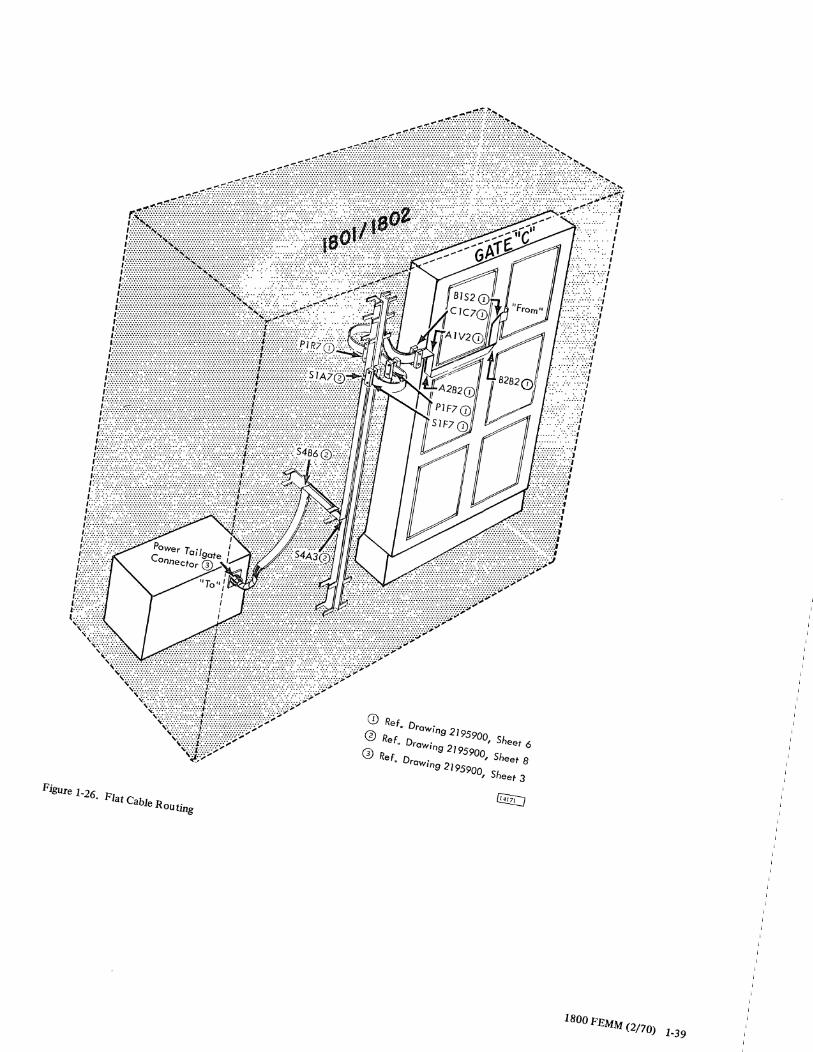
Figure 1-26. Flat Cable Routing
CD Ref. DrOWing 2/95900, Sheet 6
@ Ref. Drowing 2/95900, Sheet 8
CD Ref. DrOWing 2/95900, Sheet 3
1800 FEMM (2170) 1-39
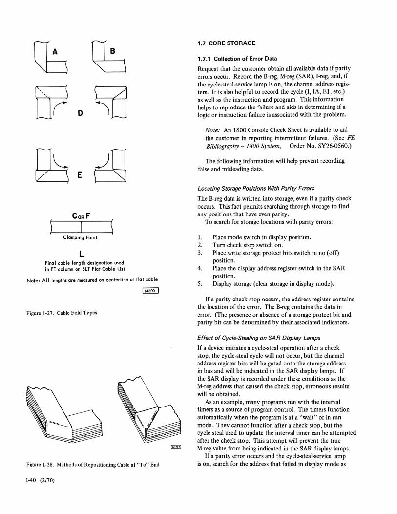
E
Clamping Point
L Fino I cable length designation used in FT column on SlT Flat Cable list
Note: All lengths are measured on centerline of flat cable
114200 I
Figure 1-27. Cable Fold Types
Figure 1-28. Methods of Repositioning Cable at "To" End
1-40 (2/70)
1.7 CORE STORAGE
1.7.1 Collection of Error Data
Request that the customer obtain all available data if parity errors occur. Record the B-reg, M-reg (SAR), I-reg, and, if the cycle-steal-service lamp is on, the channel address registers. It is also helpful to record the cycle (I, lA, EI, etc.) as well as the instruction and program. This information helps to reproduce the failure and aids in determining if a logic or instruction failure is associated with the problem.
Note: An 1800 Console Check Sheet is available to aid the customer in reporting intermittent failures. (See FE Bibliography - 1800 System, Order No. SY26-OS60.)
The following information will help prevent recording false and misleading data.
Locating Storage Positions With Parity Errors
The B-reg data is written into storage, even if a parity check occurs. This fact permits searching through storage to find any positions that have even parity.
To search for storage locations with parity errors:
1. Place mode switch in display position. 2. Tum check stop switch on. 3. Place write storage protect bits switch in no (off)
position. 4. Place the display address register switch in the SAR
position. 5. Display storage (clear storage in display mode).
If a parity check stop occurs, the address register contains the location of the error. The B-reg contains the data in error. (The presence or absence of a storage protect bit and parity bit can be determined by their associated indicators.
Effect of Cycle-Stealing on SAR Display Lamps
If a device initiates a cycle-steal operation after a check stop, the cycle-steal cycle will not occur, but the channel address register bits will be gated onto the storage address in bus and will be indicated in the SAR display lamps. If the SAR display is recorded under these conditions as the M-reg address that caused the check stop, erroneous results will be obtained.
As an example, many programs run with the interval timers as a source of program control. The timers function automatically when the program is at a "wait" or in run mode. They cannot function after a check stop, but the cycle steal used to update the interval timer can be attempted after the check stop. This attempt will prevent the true M-reg value from being indicated in the SAR display lamps.
If a parity error occurs and the cycle-steal-service lamp is on, search for the address that failed in display mode as
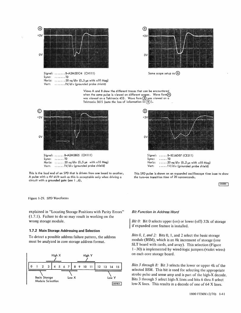
® +3V
OV
Signal: · ...... B-A2M3D04 (CH 111) Same scope setup as @ Sync: ....... TO Horiz: · ...... 50 ns/div (0.5 fls with xl 0 Mog) Vert: ....... 1V/div (grounded probe shield)
Views A and B show the different traces that can be encountered when the same pulse is viewed on different scopes. Wave form@ was viewed on a Tektronix 453. Wave form ® was viewed on a Tektronix 561 S (note the loss of information in ®)._
© +3V
OV
Signol: Sync: Horiz: Vert:
....•. B-A2M3B05 (CHIll)
...... TO
...... 50 ns/div (0.5 fls with xl0 Mag) · ..... IV/div (grounded probe shield)
This is the load end of an SPD that is driven from one board to another. A pulse with a 4V shift such as this is acceptable only when driving a circuit with a grounded gate (see 1 .6). '
Figure 1-29. SPD Waveforms
explained in "Locating Storage Positions with Parity Errors" (1.7.1). Failure to do so may result in working on the wrong storage module.
1.7.2 Main Storage Addressing and Selection
To detect a possible address failure pattern, the address must be analyzed in core storage address format.
High X High Y
I I
71 8 9 10 11 .12 13 14 15
\ Basic Storage
\ Low X
\ Low Y
Module Selection 128090A I
Signal: Sync: Horiz: Vert:
..... B-B2J6D07 (CE31l)
..... TO
..... 20 ns/div (0.2 flS with xl0 Mag)
..... 1 V/div (grounded probe shield)
This SPD pulse is shown on an expanded osci 1I0scope time base to show the turn-on transition time of 20 nanoseconds.
Bit Function in Address Word
J Bit 0: Bit 0 selects upper (on) or lower (off) 32k of storage if expanded core feature is installed.
Bits 0, 1, and 2: Bits 0, 1, and 2 select the basic storage module (BSM), which is an 8k increment of storage (one SLT board with cards, and array). This selection (Figure 1-30) is implemented by wired-logic jumpers (Violet wires) on each core storage board.
Bits 3 through 8: Bit 3 selects the lower or upper 4k of the selected BSM. This bit is used for selecting the appropriate strobe pulse and sense amp and is part or the high-X decode. Bits 3 through 5 select high-X lines and bits 6 thru 8 select low-X lines. This results in a decode of one of 64 X lines.
1800 FEMM (2/70) 1-41
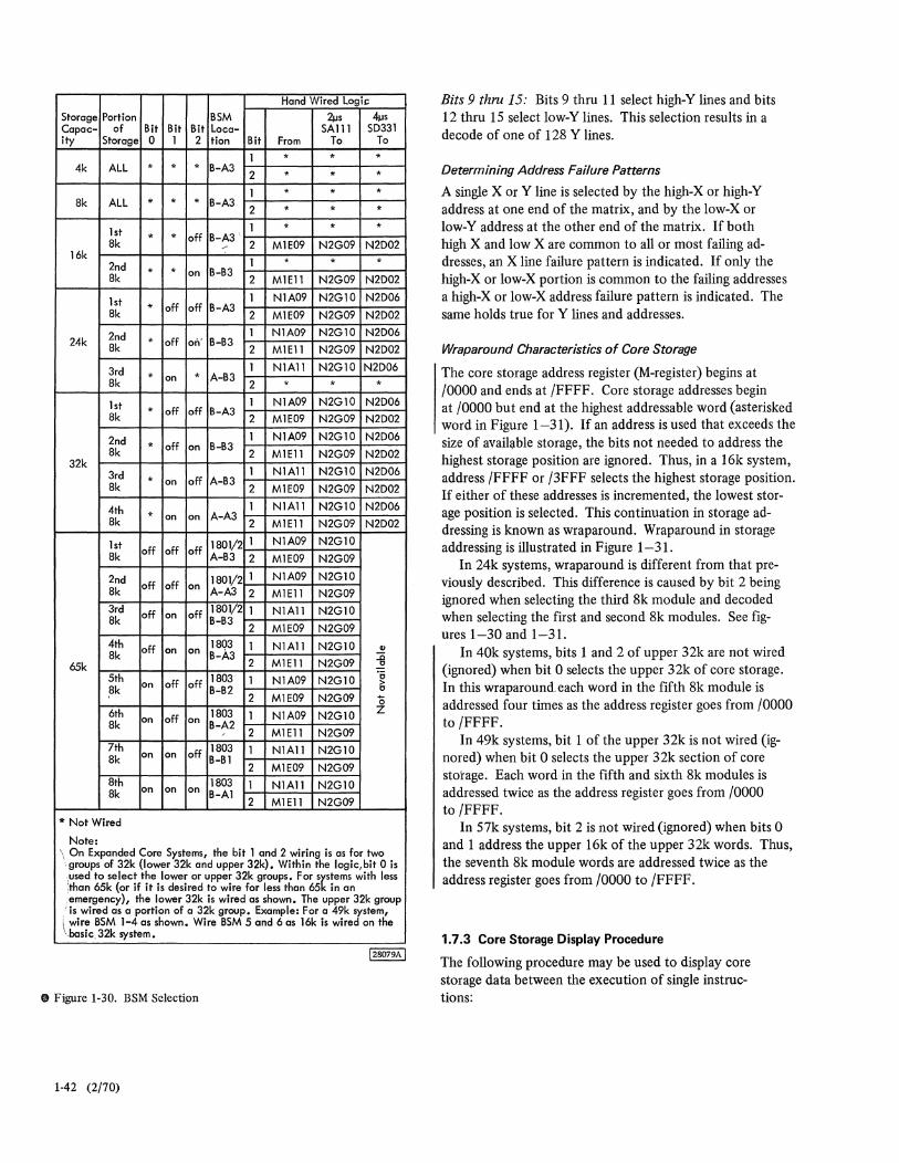
Hand Wired logil:
Storage Portion BSM ~s 4,is Capac- of Bit Bit Bit loca- SAlll SD331 ity Storage 0 1 2 tion Bit From To To
1 • * * 4k ALL * * * B-A3
2 • * * 1 • * *
Sk All * * * B-A3 2 • * *
1st 1 • * * * * off B-A3 '
Sk ': 2 M1E09 N2G09 N2D02 16k
1 * * * 2nd * * B-B3 Sk on
2 M1Ell N2G09 N2D02
1st 1 N1A09 N2Gl0 N2D06 * off off B-A3 Sk 2 M1E09 N2G09 N2D02
2nd 1 N1A09 N2Gl0 N2D06 24k • off orr B-B3 Sk 2 M1Ell N2G09 N2D02
3rd 1 NIAll N2Gl0 N2D06 * * A-B3 Sk on
2 • * * 1st 1 N1A09 N2Gl0 N2D06
* off off B-A3 Sk 2 M1E09 N2G09 N2D02
2nd 1 N1A09 N2Gl0 N2D06 * off B-B3 Sk on
2 M1Ell N2G09 N2D02 32k
1 NIAll N2Gl0 N2D06 3rd * off A-B3 Sk on
2 M1E09 N2G09 N2D02
4th 1 NIAll N2Gl0 N2D06 * A-A3 Sk on on
2 M1Ell N2G09 N2D02
1st IS01/2 1 N1A09 N2Gl0 Sk off off off A-B3 2 M1E09 N2G09
2nd 1801/2 1 N1A09 N2Gl0 Sk off off on A-A3 2 M1Ell N2G09 3rd off off IS0y21 NIAll N2Gl0 Sk on
B-B3 2 M1E09 N2G09
4th off ISQ3 1 NIAll N2Gl0 co Sk on on B-A3 ::c
65k 2 M1Ell N2G09 " 5th IS03- 1 N1A09 N2Gl0
·0 off off >
,Sk on
B-B2 " 2 M1E09 N2G09 '0 6th IS03 1 N1A09 N2Gl0 Z Sk on off on B-A2 , 2 M1Ell N2G09 7th
off IS03 1 NIAll N2Gl0 Sk on on B-Bl
2 M1E09 N2G09 Sth IS03 1 NIAll N2Gl0 Sk on on on B-Al
2 M1Ell N2G09
* Not Wired
Note: \ On Expanded Core Systems, the bit 1 and 2 wiring is as for two "groups of 32k (lower 32k and upper 32k). Within the I"gic/bit 0 is "used to select the lower or upper 32k groups. For s~stems with less ;than 65k (or if it is desired to wire for less than 65 in an ;emergency), the lower 32k is wired as shown. The upper 32k group
,I is wired as a portion of a 32k group. Example: For a 49k system, \ wire BSM 1-4 as shown. Wire BSM 5 and 6 as 16k is wired on the .basic_ 32k system.
• Figure 1-30. BSM Selection
1-42 (2/70)
Bits 9 thru 15: Bits 9 thru 11 select high-Y lines and bits 12 thru 15 select low-Y lines. This selection results in a decode of one of 128 Y lines.
Determining Address Failure Patterns
A single X or Y line is selected by the high-X or high-Y address at one end of the matrix, and by the low-X or low-Y address at the other end of the matrix. If both high X and low X are common to all or most failing addresses, an X line failure pattern is indicated. If only the high-X or low-X portion is common to the failing addresses a high-X or low-X address failure pattern is indicated. The same holds true for Y lines and addresses.
Wraparound Characteristics of Core Storage
The core storage address register (M-register) begins at /0000 and ends at /FFFF. Core storage addresses begin at /0000 but end at the highest addressable word (asterisked word in Figure 1-31). If an address is used that exceeds the size of available storage, the bits not needed to address the highest storage position are ignored. Thus, in a 16k system, address /FFFF or /3FFF selects the highest storage position. If either of these addresses is incremented, the lowest storage position is selected. This continuation in storage addressing is known as wraparound. Wraparound in storage addressing is illustrated in Figure 1-31.
In 24k systems, wraparound is different from that previously described. This difference is caused by bit 2 being ignored when selecting the third 8k module and decoded when selecting the first and second 8k modules. See figures 1-30 and 1-31.
In 40k systems, bits 1 and 2 of upper 32k are not wired (ignored) when bit a selects the upper 32k of core storage. In this wraparound, each word in the fifth 8k module is addressed four times as the address register goes from /0000 to /FFFF.
In 49k systems, bit 1 of the upper 32k is not wired (ignored) when bit a selects the upper 32k section of core storage. Each word in the fifth and sixth 8k modules is addressed twice as the address register goes from /0000 to /FFFF.
In 57k systems, bit 2 is not wired (ignored) when bits a and 1 address the upper 16k of the upper 32k words. Thus, the seventh 8k module words are addressed twice as the address register goes from /0000 to /FFFF.
1.7.3 Core Storage Display Procedure
The following procedure may be used to display core storage data between the execution of single instructions:
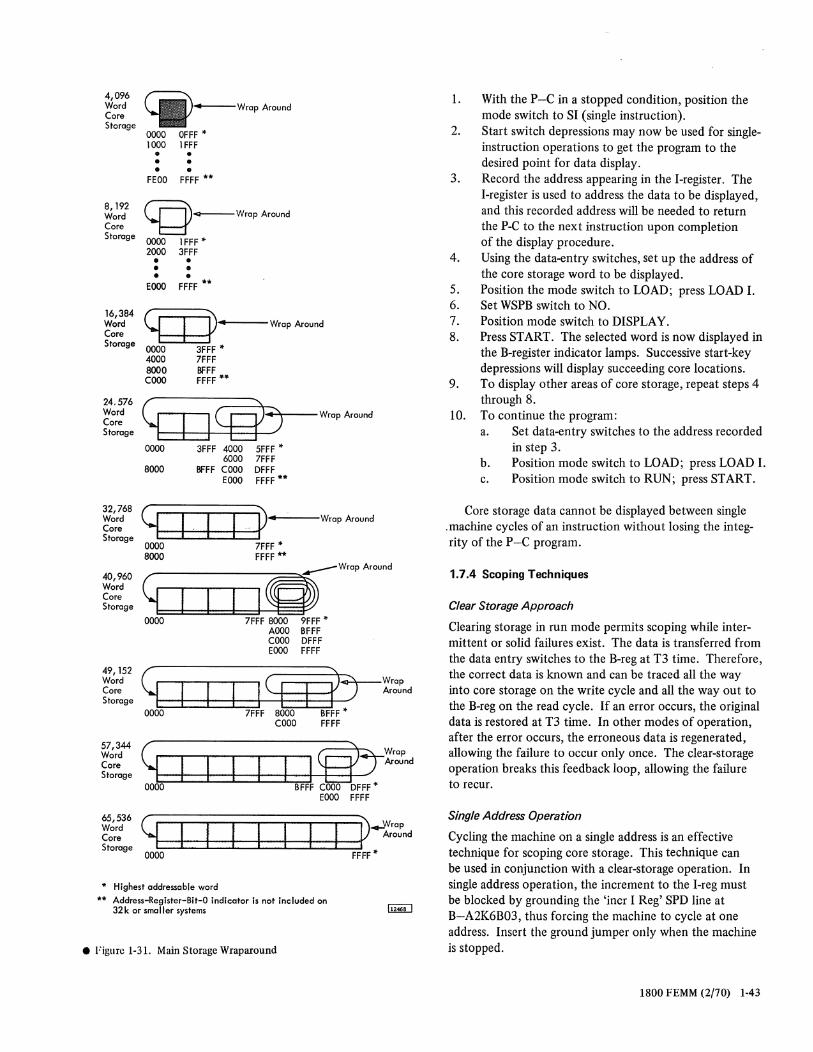
4,096 Word Core Storage
8, 192 Word Core Storage
16,384 Word Core Storage
24.576 Word Core Starage
32,768 Word Core Storage
40,960 Word Core Storage
49,152 Word Core Storage
57,344 Word Core Storage
65,536 Word Core Storage
l"--wr<", Around
0000 OFFF" 1000 lFFF • • • • • •
FEOO FFFF **
4---Wrop Around cgQ 0000 lFFF" 2000 3FFF • • • • • •
EOOO FFFF **
~ P4 Wrap Around
0000 3FFF" 4000 7FFF 8000 BFFF COOO FFFF ..
~ I~") Wrap Around
0000 3FFF 4000 5FFF .. 6000 7FFF
8000 BFFF COOO DFFF EOOO FFFF **
q I I I " P4 Wrap Around
0000 7FFF .. 8000 FFFF **
~ ..---Wrap Around
10 0000 7FFF 8000 9FFF"
AOOO BFFF COOO DFFF EOOO FFFF
~kd=:d:d::d:-I C::::EI ~rT~"d 0000 7FFF 8000 BFFF ..
COOO FFFF
~ 0000
IgJ-zr:nd
BFFF COOO DFFF .. EOOO FFFF
q I I I I ~round p __ wrap
0000 FFFF ..
* Highest addressable word ** Address-Register-Bit-O indicator is not included on
32 k or smaller systems
• Figure 1-31. Main Storage Wraparound
1.
2.
3.
With the P-C in a stopped condition, position the mode switch to SI (single instruction). Start switch depressions may now be used for singleinstruction operations to get the program to the desired point for data display. Record the address appearing in the I-register. The I-register is used to address the data to be displayed, and this recorded address will be needed to return the P-C to the next instruction upon completion of the display procedure.
4. Using the data-entry switches, set up the address of the core storage word to be displayed.
5. Position the mode switch to LOAD; press LOAD I. 6. Set WSPB switch to NO. 7. Position mode switch to DISPLAY. 8. Press START. The selected word is now displayed in
the B-register indicator lamps. Successive start-key depressions will display succeeding core locations.
9. To display other areas of core storage, repeat steps 4 through 8.
10. To continue the program: a. Set data-entry switches to the address recorded
in step 3. b. Position mode switch to LOAD; press LOAD I. c. Position mode switch to RUN; press START.
Core storage data cannot be displayed between single .machine cycles of an instruction without losing the integrity of the P-C program.
1.7.4 Scoping Techniques
Clear Storage Approach
Clearing storage in run mode permits scoping while intermittent or solid failures exist. The data is transferred from the data entry switches to the B-reg at T3 time. Therefore, the correct data is known and can be traced all the way into core storage on the write cycle and all the way out to the B-reg on the read cycle. If an error occurs, the original data is restored at T3 time. In other modes of operation, after the error occurs, the erroneous data is regenerated, allowing the failure to occur only once. The clear-storage operation breaks this feedback loop, allowing the failure to recur.
Single Address Operation
Cycling the machine on a single address is an effective technique for scoping core storage. This technique can be used in conjunction with a clear-storage operation. In single address operation, the increment to the I-reg must be blocked by grounding the 'incr I Reg' SPD line at B-A2K6B03, thus forcing the machine to cycle at one address. Insert the ground jumper only when the machine is stopped .
1800 FEMM (2/70) 1-43
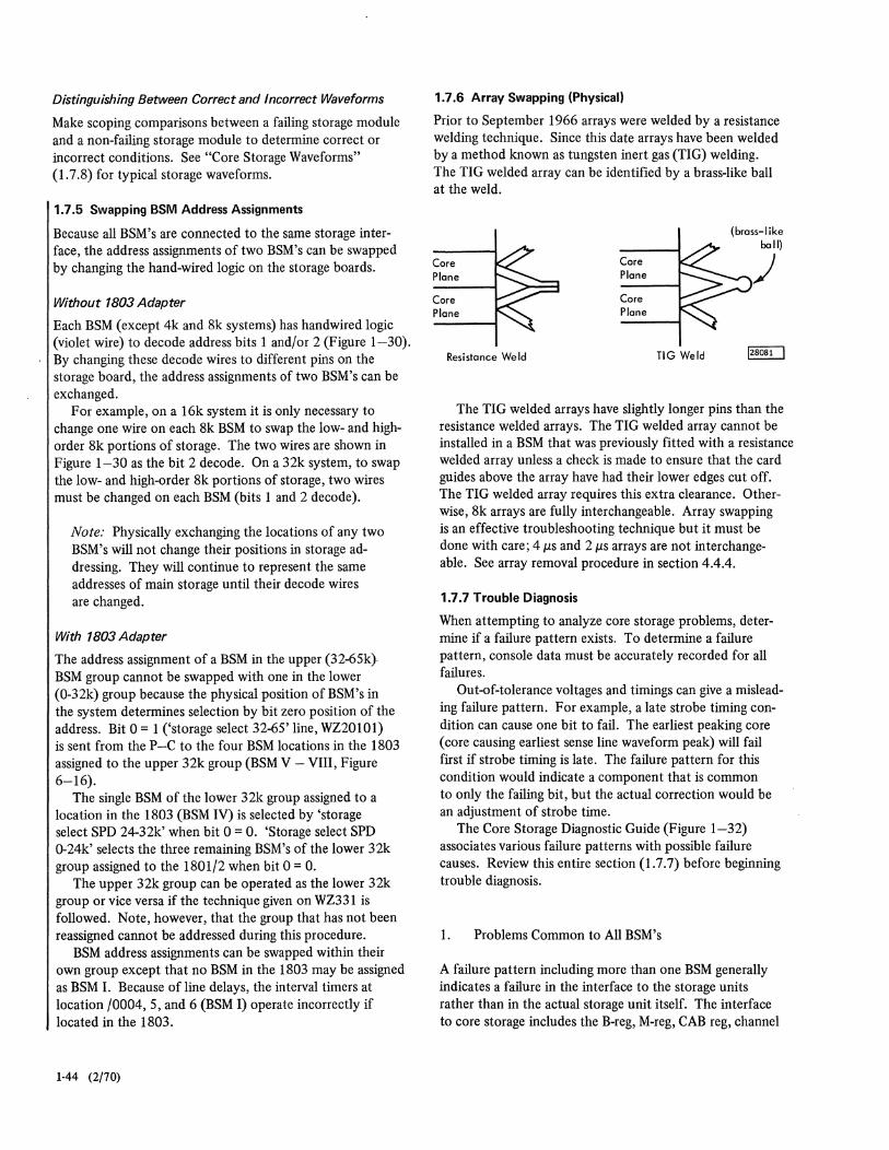
Distinguishing Between Correct and Incorrect Waveforms
Make scoping comparisons between a failing storage module and a non-failing storage module to determine correct or incorrect conditions. See "Core Storage Waveforms" (1. 7.8) for typical storage waveforms.
1.7.5 Swapping BSM Address Assignments
Because all BSM's are connected to the same storage interface, the address assignments of two BSM's can be swapped by changing the hand-wired logic on the storage boards.
Without 1803 Adapter
Each BSM (except 4k and 8k systems) has handwired logic (violet wire) to decode address bits 1 and/or 2 (Figure 1-30). By changing these decode wires to different pins on the storage board, the address assignments of two BSM's can be exchanged.
For example, on a 16k system it is only necessary to change one wire on each 8k BSM to swap the low- and highorder 8k portions of storage. The two wires are shown in Figure 1-30 as the bit 2 decode. On a 32k system, to swap the low- and high-order 8k portions of storage, two wires must be changed on each BSM (bits 1 and 2 decode).
Note: Physically exchanging the locations of any two BSM's will not change their positions in storage addressing. They will continue to represent the same addresses of main storage until their decode wires are changed.
With 1803 Adapter
The address assignment of a BSM in the upper (32-65k). BSM group cannot be swapped with one in the lower (0-32k) group because the physical position of BSM's in the system determines selection by bit zero position of the address. Bit 0 = 1 ('storage select 32-65' line, WZ20101) is sent from the P-C to the four BSM locations in the 1803 assigned to the upper 32k group (BSM V - VIII, Figure 6-16).
The single BSM of the lower 32k group assigned to a location in the 1803 (BSM IV) is selected by 'storage select SPD 24-32k' when bit 0 = O. 'Storage select SPD 0-24k' selects the three remaining BSM's of the lower 32k group assigned to the 1801/2 when bit 0 = O.
The upper 32k group can be operated as the lower 32k group or vice versa if the technique given on WZ331 is followed. Note, however, that the group that has not been reassigned cannot be addressed during this procedure.
BSM address assignments can be swapped within their own group except that no BSM in the 1803 may be assigned as BSM I. Because of line delays, the interval timers at location /0004, 5, and 6 (BSM I) operate incorrectly if located in the 1803.
1-44 (2/70)
1.7.6 Array Swapping (Physical)
Prior to September 1966 arrays were welded by a resistance welding technique. Since this date arrays have been welded by a method known as tungsten inert gas (TlG) welding. The TlG welded array can be identified by a brass-like ball at the weld.
Care Plane
Care Plane
Resistance Weld
Care Plane
Care Plane
TlG Weld
(brass-like ball)
)
The TlG welded arrays have slightly longer pins than the resistance welded arrays. The TlG welded array cannot be installed in a BSM that was previously fitted with a resistance welded array unless a check is made to ensure that the card guides above the array have had their lower edges cut off. The TlG welded array requires this extra clearance. Otherwise, 8k arrays are fully interchangeable. Array swapping is an effective troubleshooting technique but it must be done with care; 4 p.s and 2 p.s arrays are not interchangeable. See array removal procedure in section 4.4.4.
1.7.7 Trouble Diagnosis
When attempting to analyze core storage problems, determine if a failure pattern exists. To determine a failure pattern, console data must be accurately recorded for all failures.
Out-of-tolerance voltages and timings can give a misleading failure pattern. For example, a late strobe timing condition can cause one bit to fail. The earliest peaking core (core causing earliest sense line waveform peak) will fail first if strobe timing is late. The failure pattern for this condition would indicate a component that is common to only the failing bit, but the actual correction would be an adjustment of strobe time.
The Core Storage Diagnostic Guide (Figure 1-32) associates various failure patterns with possible failure causes. Review this entire section (1.7.7) before beginning trouble diagnosis.
1. Problems Common to All BSM's
A failure pattern including more than one BSM generally indicates a failure in the interface to the storage units rather than in the actual storage unit itself. The interface to core storage includes the B-reg, M-reg, CAB reg, channel
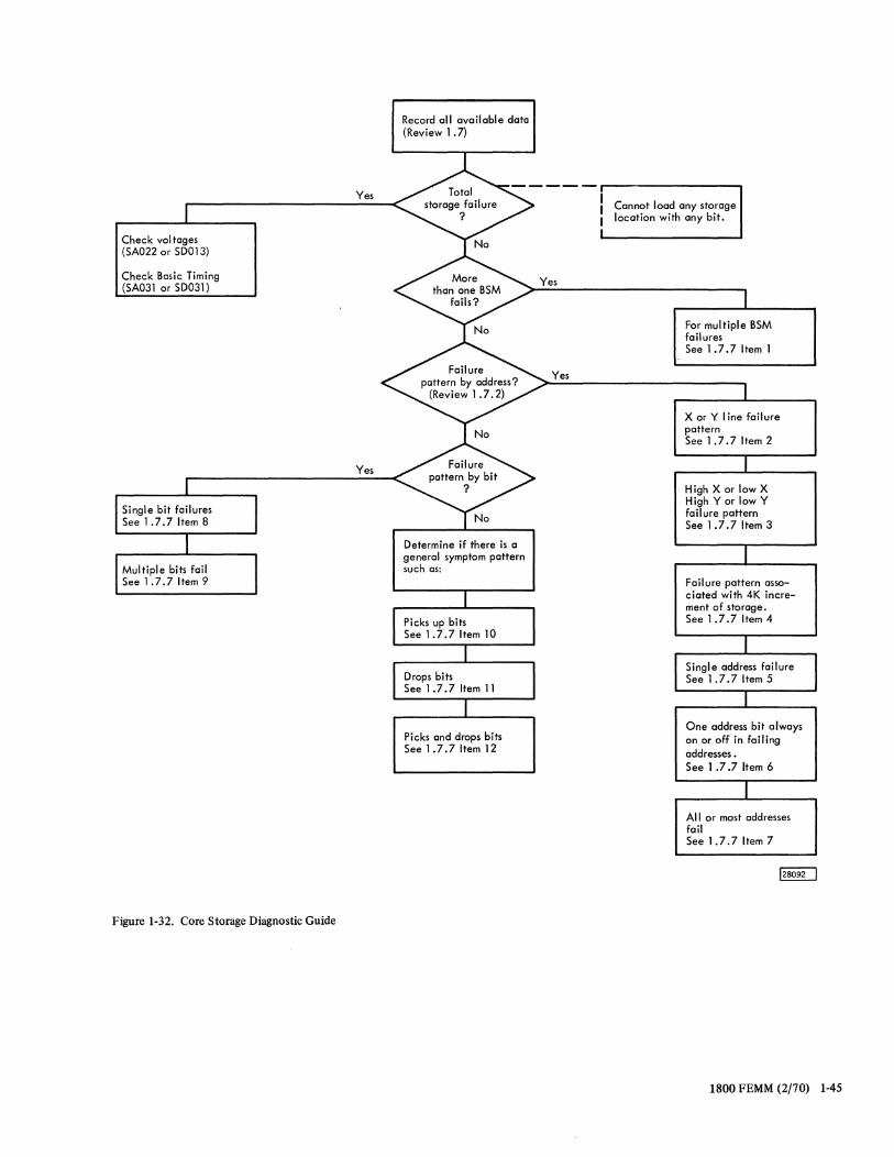
Check vol tages (SA022 or SDOI3)
Check Basic Timing (SA031 or SD031)
Figure 1-32. Core Storage Diagnostic Guide
Yes
Yes
Record all available data (Review 1.7)
Determine if there is a general symptom pattern such as:
Picks and drops bits See 1.7.7 Item 12
Cannot load any storage location with any bit.
For multiple BSM failures See 1 .7.7 I tern 1
X or Y I ine failure pattern See 1.7.7 Item 2
High X or low X High Y or low Y failure pattern See 1 .7.7 I tern 3
Failure pattern associated with 4K increment of storage. See 1.7.7 Item 4
One address bit always on or off in fai ling addresses. See 1 .7.7 Item 6
Allor most addresses fail See 1 .7.7 I tern 7
1800 FEMM (2/70) 1-45
address registers, cables, connectors, and general control signals.
Check address bits for proper timing and level. To check timing, clear storage to /6000. At storage location /0000 and /0001 enter /6400 and /7FFF respectively. Place mode switch in run, reset and push start. This permits scoping of the address bits (cannot be done in clear-storage mode). These bits have critical timing requirements. Bits I and 2 have earlier timings than the other bits and must be present (at decision level) before the 1.8V level of 'storage select' (2 p.s) or 'read cycle' (4 p.s) time. The other bits must be stable 25 nanoseconds after the 1.8V level of 'storage select' (2 p.s) or 'read cycle' (4 p.s).
Check basic core storage voltages (SA022 or SD013).
2. X or Y Line Failure Pattern
I Check the driver and gate cards by substituting a new card or interchanging cards of the same type. To check for an open line or defective line weld, check continuity of the line through the array (line path example is given on SAOl2 or SDOI2).
The following are typical resistances for X or Y lines. The measurements are made from one end of the line to the other end of the line with no diodes in the circuit.
Y-drive line: X-drive line:
8k
5 ohms 8.5 ohms
4k
2.5 ohms 8.5 ohms
High resistance in the drive line can cause dropping of bits. The high resistance can be caused by poor line welds, high-resistance bottom board pins, poor connection in the connector block, or by a defective diode.
The most difficult drive line problem to diagnose is the defective diode, which can cause several different failure symptoms. There are two diodes associated with each drive line, one for read and one for write. Either can cause a problem but the read diode is more critical. A change in the diode response time will change the timing of the sense-line wave form. The read diode is more critical to response time because the sense line waveform must be timed properly to the strobe pulse.
A diode having iniproper resistance can usually be detected by a static resistance check. Compare the suspected diode with the readings of other diodes in the BSM. However, a diode with poor response time will usually measure good with a static check and will usually operate properly in a sequential addreSSing mode, such as display mode. However. it may fail to conduct properly in certain program loops. It may be possible to detect a faulty read diode by moving the strobe later by approximately 20 nanoseconds. If this adjustment improves operation, it is possible that a diode with poor response time has caused the core output to be later
1-46 (2/70)
and more compatible with the later strobe. A write diode failure will not be affected by strobe timing.
A high-resistance or poor-response-time diode will have an X- or Y-drive line failure pattern. A shorted diode will have a failure pattern including most drive lines (Figures 1-36 and 1-45). If a problem can be related to a suspected diode, replace the diode. For diode replacement information, see 4.4.6.
Check for leakage between the X or Y line and a sense line as explained in item 8.
Scope the failing storage module using the techniques explained in 1.7.4.
3. High-X or Low-X, High-Y or Low-Y Failure Pattern
Possible causes are driver or gate cards, defective connector block, defective diode (see item 2), current balance (2 p.s storage units), or bottom board leakage (see item 8).
Try replacing suspected card or connector. Scope failing addresses.
4. 4k Increment Failure Pattern
This could be associated with address bit 3 or the 'less than 4k' or 'greater than 4k' strobe. Check the strobe pulse and strobe timing.
If failure is bit-oriented it could be caused by a defective sense amp, inhibit driver, or sense line. There is one inhibit driver for each of the 18 bit positions in each 4k of storage. If an inhibit driver never conducts, that bit position enters 4k of storage continuously. If it always conducts, the bit can never be entered into that 4k. Any other 4k segment of core functions correctly. If there is a bit failure through 4k of core, replace the inhibit driver and sense amplifier cards for that bit position. If the trouble is not a card, but sense/inhibit failure is suspected, check the continuity of the sense/inhibit line. See item 8 for discussion of single bit failures and sense line resistance measurements.
5. Single-Address Failures
This kind of failure is often the result of a weak or earlypeaking core whose output is made more marginal by low VRef(determines'drive current level) or poor current balance (2 p.s storage units). Other causes can be a late strobe, high Vsa - Ve (determines sense-amp threshold for 1 bit, adjustable only in 4 p.s storage), or a large deviation from a nominal (60°F - 90°F) room environment.
As temperature increases, cores peak earlier and higher, but ideally the strobe does not change its timing. The strobed signal is therefore lower at increased temperatures because the strobe occurs later in the signal.
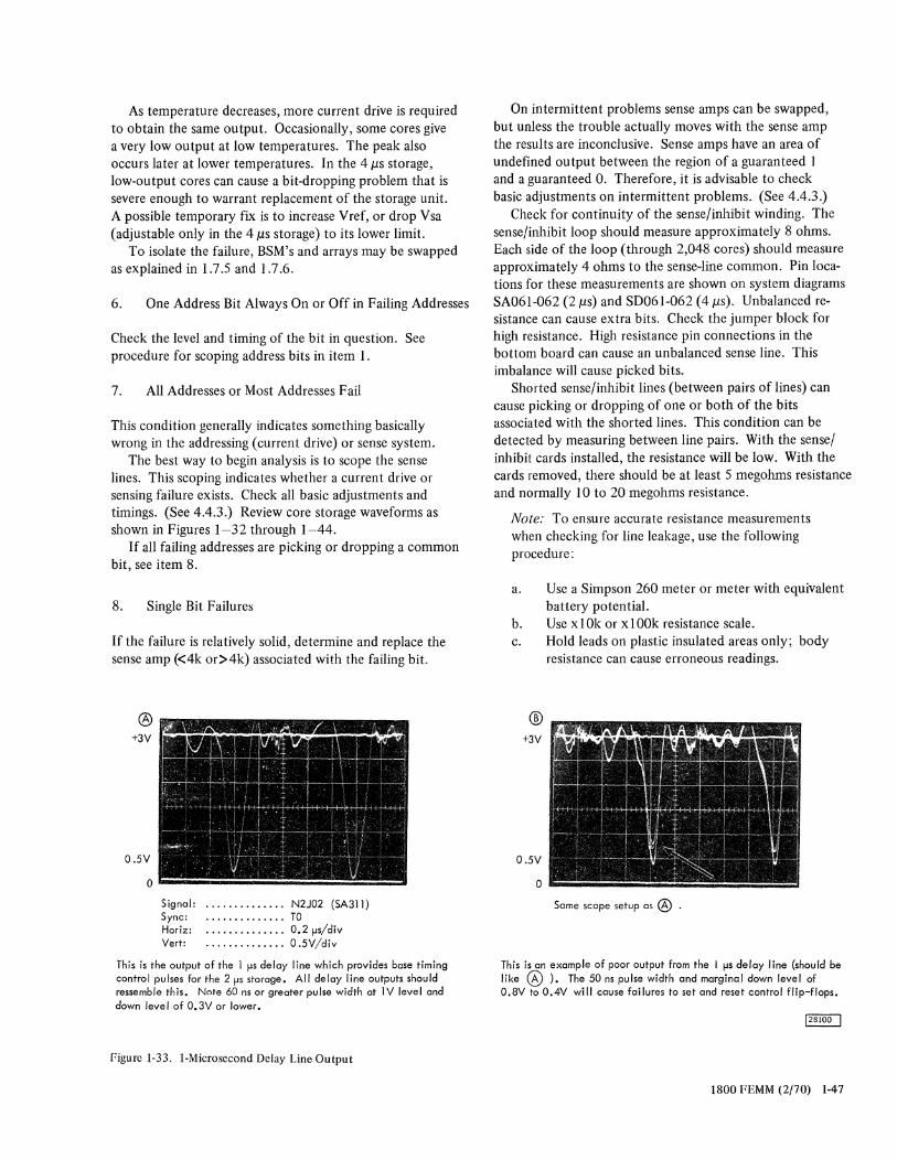
As temperature decreases, more current drive is required to obtain the same output. Occasionally, some cores give a very low output at low temperatures. The peak also occurs later at lower temperatures. In the 4 J.1s storage, low-output cores can cause a bit-dropping problem that is severe enough to warrant replacement of the storage unit. A possible temporary fix is to increase Vref, or drop Vsa (adjustable only in the 4J.1s storage) to its lower limit.
To isolate the failure, BSM's and arrays may be swapped as explained in 1.7.5 and 1.7.6.
6. One Address Bit Always On or Off in Failing Addresses
Check the level and timing of the bit in question. See procedure for scoping address bits in item 1.
7. All Addresses or Most Addresses Fail
This condition generally indicates something basically wrong in the addressing ( current drive) or sense system.
The best way to begin analysis is to scope the sense lines. This scoping indicates whether a current drive or sensing failure exists. Check all basic adjustments and timings. (See 4.4.3.) Review core storage waveforms as shown in Figures 1-32 through 1-44.
If all failing addresses are picking or dropping a common bit, see item 8.
8. Single Bit Failures
If the failure is relatively solid, determine and replace the sense amp «4k or>4k) associated with the failing bit.
® +3V
O.SV
o liiiiiiiiiiiiiiiiiiiiii Signal: Sync: Horiz: Vert:
. . . . . . . . . . . . .. N2J02 (SA31l)
.............. TO
.............. 0.2 flS/div
.............. O.SV/div
This is the output of the 1 flS delay line which provides base timing control pulses for the 2 flS storage. All delay line outputs should ressemble this. Note 60 ns or greater pulse width at 1 V level and down level of 0.3V or lower.
Figure 1-33. I-Microsecond Delay Line Output
On intermittent problems sense amps can be swapped, but unless the trouble actually moves with the sense amp the results are inconclusive. Sense amps have an area of undefined output between the region of a guaranteed 1 and a guaranteed O. Therefore, it is advisable to check basic adjustments on intermittent problems. (See 4.4.3.)
Check for continuity of the sense/inhibit winding. The sense/inhibit loop should measure approximately 8 ohms. Each side of the loop (through 2,048 corcs) should measure approximately 4 ohms to the sense-line common. Pin locations for these measurements are shown on system diagrams SA061-062 (2 J.1s) and SD06J-062 (4,us). Unbalanced resistance can cause extra bits. Check the jumper block for high resistance. High resistance pin connections in the bottom board can cause an unbalanced sense line. This imbalance will cause picked bits.
Shorted sense/inhibit lines (between pairs of lines) can cause picking or dropping of one or both of the bits associated with the shorted lines. This condition can be detected by measuring between line pairs. With the sensei inhibit cards installed, the resistance will be low. With the cards removed, there should be at least 5 megohms resistance and normally 10 to 20 megohms resistance.
Note: To ensure accurate resistance measurements when checking for line leakage, use the following procedure:
a.
b. c.
® +3V
O.SV
o
Use a Simpson 260 meter or meter with equivalent battery potential. Use x 1 Ok or x lOOk resistance scale. Hold leads on plastic insulated areas only; body resistance can cause erroneous readings.
Same scope setup as ® .
This is an example of poor output from the 1 fls delay line (should be like 0 ). The SO ns pulse width and marginal down level of 0.8V to O.4V will cause failures to set and reset control flip-flops.
1800 FEMM (2/70) 1-47
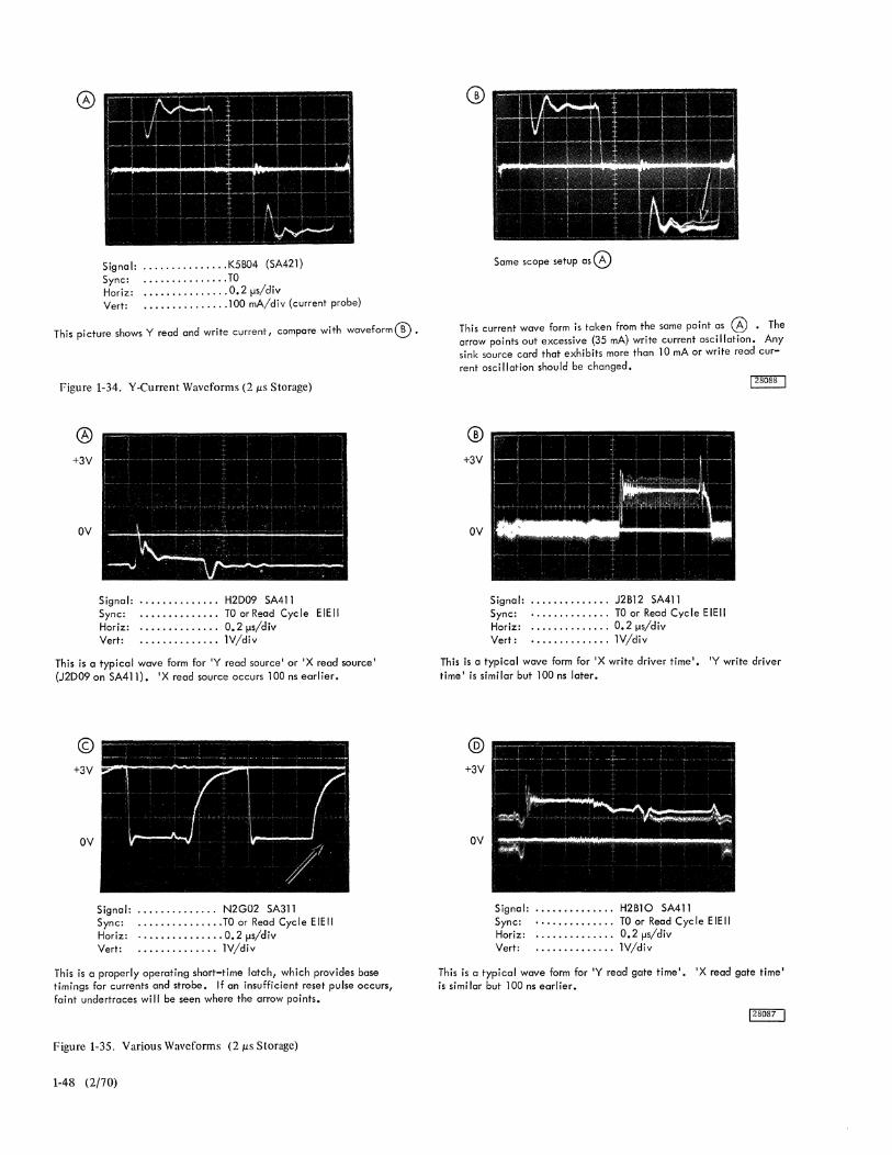
o
Signal: Sync: Horiz: Vert:
............... K5B04 (SA42l)
............... TO
............... 0.2 flS/div
............... 100 mA/div (current probe)
This picture shows Y read and write current, compare with waveform® .
rigure 1-34. Y-Current Waveforms (2 j.LS Storage)
Signal: Sync: Horiz: Vert:
H2D09 SA411 TO or Read Cycle EIEII 0.2 fls/div lV/div
This is a typical wave form far 'Y read source' ar 'X read saurce' (J2D09 on SA41 1 ). 'X read source occurs 100 ns earlier.
© +3V
OV
Signol: Sync: Horiz: Vert:
.............. N2G02 SA311
............... TO or Read Cycle EIEII
............... 0.2 flS/div
.............. lV/div
This is a properly operating short-time latch, which provides base timings for currents ond strobe. If an insufficient reset pulse occurs, faint undertraces will be seen where the arrow points.
Figure 1-35. Various Waveforms (2 j.LS Storage)
1-48 (2/70)
Same scope setup as 0
This current wave form is taken from the same point as @ . The arrow points out excessive (35 mAl write current asci Ilation. Any sink source card that exhibits more than 10 mA or write read current oscillation should be changed.
® +3V
OV
Signal: Sync: Horiz: Vert :
J2B12 SA411 TO or Read Cycle EIEII 0.2 fls/div lV/div
This is a typical wave form for 'X write driver time'. 'Y write driver time' is similar but 100 ns later.
@ +3V
OV
Signal: Sync: Horiz: Vert:
H2B10 SA411 TO or Read Cycle EIEII 0.2 flS/div lV/div
This is a typical wave form for 'Y read gate time'. 'X read gate time' is simi lar but 100 ns earlier.
d. Allow meter to remain attached to points being measured for at least 30 seconds if less than several megohms is initially measured. If leakage does exist, a breakdown phenomenon can occur, causing reading to drop after a period of time.
Leakage can occur between a sense line and an X-drive line. Check this condition as follows:
a. Remove sense-line connector block associated with bit to be checked (SA061-062 or SD061-062).
b. Check for resistance between the sense line of the failing bit and the following driver gate pins:
2-Microsecond Storage Units M3B12,L3DOS,F2DOS,F2BOS
4-Microsecond Storage Units J3DlO, K3D06, J2DlO, J2BOS
BSM bottom board leakage can occur between a sense line and an X or Y line and will be related to a low- or high- order X or Y address. Check for this leakage as follows:
a. Remove sense line connector block associated with bit to be checked. (SA061-062 or SD061-062).
b. Check for resistance between the sense line of the failing bit and the following pins:
2-Microsecond Storage Units
Card Sockets
C3,D3 E3,F3 L3,M3
G3,H3 J3,K3
Pins in Each Socket
B12, DOS D10,Dll
B03,B04 BOS,B12 D04,DOS D10,Dll
4-Microsecond Storage Units
Card Sockets
C3,D3 E3,F3 J3,K3
Pins in Each Socket
B08,DOS D06,D10
G3,H3 L3,M3
B04,BOS B08,B12 B13, DOS D06,D10
The readings obtained in the previous checks should be approximately 5 to 50 megohms. A unit with lOOk ohms resistance will work but experience has shown that units with a leakage path lower than several megohms will continue to deteriorate and eventually cause intermittent parity errors. Defective units have also exhibited a momentary breakdown from 5 megohms to Sk ohms under heat, vibration, or extended operation.
Storage adjustment or card swapping can affect a problem caused by sense-line-to-sense-line or sense-line-to-drive-line leakage, but storage replacement is the only permanent solution. Before a storage unit is replaced for leakage, it should be thoroughly checked to ensure that leakage is not caused by external components such as connector pins or connector blocks.
9. Multiple Bits Fail
This condition generally suggests a basic problem in current drive or sensing. Determine whether failing bits share connectors or SLT cards. If no obvious cause is found, check strobe timing and sense line and current waveforms. For core storage waveforms see 1.7.8.
Determine if an address failure pattern exists.
10. Picks Up Bits
a. Low Vsa - Ve (sense level control voltage - offset voltage, sets threshold of a 1 in sense amp).
b. Strobe early. c. Unbalanced sense line (item 8). d. Leakage from drive line. (See item 8.) e. Double strobe (logic failure). f. Current drive high. (Vref determines current
level.) g. Defective diode. (See item 2.)
11. Drops Bits
a. Weak core (one address, one bit). b. High Vsa - Ve. (See item 10.) c. Strobe late. d. Leakage from drive line. (See item 8.) e. Current drive low. (Vref determines current
level.) f. Defective diode. (See item 2.)
1800 FEMM (2/70) 1-49
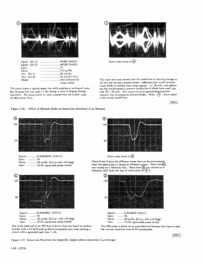
Signal (Ch 1): Signal (Ch 2): Sync: Horiz: Vert (Ch I): Vert (Ch 2): Mode:
.............. • M7B02 (SA561) •........•..•.. M7D02 (SA561) •.....•..••.•.• TO ....•..•...•.•• 0.2 flS/div •...........•.. 20 mV/div ............... 20 mV/div (Inv) •.•.....•..••.. Add (differential
scope cable)
This photo shows a typical sense line while reading or writing all ones. Bit-14 sense line was used ( < 4k) during a clear or display storage operation. The arrow points to noise coupled from the inhibit noise of other sense lines.
Same scope setup as ® .
This wave form was viewed with the conditions of clearing storage to all bits and having a shorted diode. Addresses that would normally cause diode to conduct have large signals. « 50 mY), and addresses that would normally prevent conduction of diode have small signals (20 - 30 mY). This causes the picking-and-dropping-bits symptom that accompanies shorted diodes. Photo @ shows signal under normal conditions.
Figure 1-36. Effect of Shorted Diode on Sense-Line Waveform (2 /.lS Storage)
@ ® +3V +3V
OV OV
Signal: Sync: Horiz: Vert:
© +3V
OV
Signal: Sync: Horiz: Vert:
....... B-A2M3D04 (CHIlI)
....... TO •.•••.. 50 ns/div (0.5 fls with xlO Mag) .•.•.•. IV/div (grounded probe shield)
...... B-A2M3B05 (CHlll)
...... TO
..•..• 50 ns/div (0.5 flS with xlO Mag)
.•.... IV/div (grounded probe shield)
Same scope setup as @
Views A and B show the different traces that can be encountered when the same pulse is viewed on different scopes. Wave form@ was viewed on a Tektronix 453. Wave form ® was viewed on a Tektronix 561S (note the loss of information in ®).
Signal: Sync: Horiz: Vert:
••••• B-B2J6D07 (CE311) ..... TO ••••• 20 ns/div (0.2 flS with xlO Mag) ••••. I V/div (grounded probe shield)
This is the load end of an SPD that is driven from one board to another. A pulse with a 4V shift such as this is acceptable only when driving a circuit with a grounded gate (see I .6).
This SPD pulse is shown on an expanded osci 1I0scope time base to show the turn-on transition time of 20 nanosecands.
Figure 1-37. Sense Line Waveform for Single-Bit, Single-Address Operation (2 p.s Storage)
1-50 (2/70)
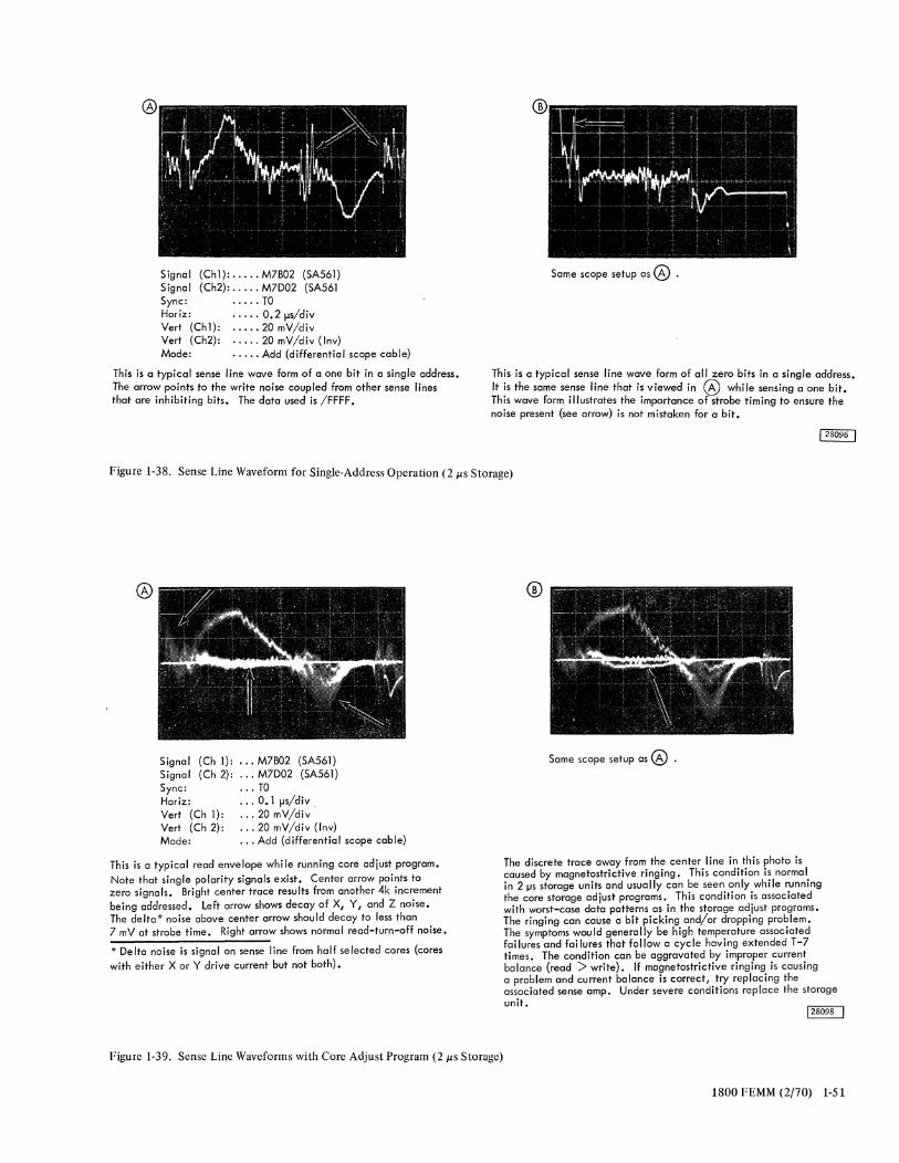
Signal Signal Sync:
(Ch 1): ..... M7B02 (SA561) (Ch2): ..... M7D02 (SA561
Horiz: Vert (Ch1): Vert (Ch2): Mode:
..... TO
...•. 0.2 fls/div
....• 20 mV/div
..... 20 mV/div (Inv)
....• Add (differential scope cable)
This is a typical sense line wave form of a one bit in a single address. The arrow points ta the write noise coupled from other sense lines that are inhibiting bits. The data used is /FFFF.
Same scope setup as ® .
This is a typical sense line wave form of all zero bits in a single address. It is the same sense line that is viewed in (£) while sensing a one bit. This wave form illustrates the importance of strobe timing to ensure the noise present (see arrow) is not mistaken for a bit.
Figure 1-38. Sense Line Waveform for Single-Address Operation (21ls Storage)
Signal Signal Sync:
(Ch 1): ... M7B02 (SA561) (Ch 2): ... M7D02 (SA561)
Horiz: Vert (Ch I): Vert (Ch 2): Mode:
... TO
... 0.1 fls/div
... 20 mV/div .
... 20 mV/div (Inv)
... Add (differential scope cable)
This is a typical read envelope whi Ie running core adiust program. Note that single polarity signals exist. Center arrow points to zero signals. Bright center trace results from another 4k increment being addressed. Left arrow shows decay of X, Y I and Z noise. The delta* noise above center arrow should decay to less than 7 mV at strobe time. Right arrow shows normal read-turn-off naise.
* Delta noise is signal on sense line from half selected cores (cores with either X or Y drive current but not both),
Figure 1-39. Sense Line Waveforms with Core Adjust Program (2 IlS Storugc)
®
Same scope setup as ® .
The discrete trace away fram the center line in this photo is caused by magnetostrictive ringing. This condition is narmal in 2IJs storage units and usually can be seen only while running the core storage adiust programs. This condition is associated with worst-case data patterns as in the storage adiust programs. The ringing can cause a bit picking and/or dropping problem. The symptoms would generally be high temperature associated failures and failures that follow a cycle having extended T-7 times. The condition can be aggravated by improper current balance (read> write). If magnetostrictive ringing is causing a problem and current balance is correct, try replacing the associated sense amp. Under severe conditions replace the storage unit •
1800 FEMM (2/70) 1-51
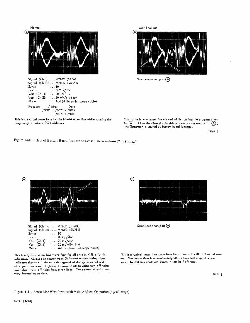
Normal
Signal Signal Sync: Horiz:
(Ch I): •.• M7B02 (SA561) (Ch 2): .•• M7D02 (SA561)
••. TO
Vert (Ch I): .•. 0.2 fls/div ••• 20 mV/div
Vert (Ch 2): ••. 20 mV/div (Inv) Mode: .•• Add (differential scope cable)
Program: Address Data /0000 to /007E = /1 002
/007F = /6000
This is a typical wave form for the bit-14 sense line whi Ie running the program given above (XOO address).
With Leakage
Same scope setup as ®
This is the bit-14 sense line viewed whi Ie running the program given in (A). Note the distortion in this picture as compared with ®. Thisdlstortion is caused by bottom board leakage.
128099 1
Figure 1-40. Effect of Bottom Board Leakage on Sense Line Waveform (2 J.LS Storage)
Signal Signal Sync:
(Ch I): .••. M7B02 (SD781) (Ch 2): .•.. M7D02 (SD781)
Horiz: Vert (Ch 1): Vert (Ch 2): Mode:
•••• TO ••.. 0.5 flS/div .•.• 20 mV/div •.•. 20 mV/div (Inv) •.•• Add (differential scope cable)
This is a typical sense line wave form for all ones in < 4k or> 4k addresses. Absence or center trace {left-most arrow} during signal indicates that this is the only 4k segment of storage selected and all signals are ones. Right-most arrow points to write turn-off noise and inhibit turn-off noise from other lines. The amount of noise can vary depending on data.
®
Same scope setup as ®
This is a typical sense line wave form for all zeros in <4k or>4k addresses. The strobe time is approximately 900 ns from left edge of scope face. Inhibit transients are sh_o~n in last halLof trace.
Figure 1-41. Sense Line Waveforms with Multi-Address Operation (4 J.LS Storage)
1-52 (2/70)
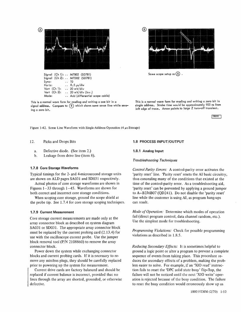
Signal (Ch 1): .. Signal (Ch 2): .. Sync: Horiz: Vert (Ch 1): Vert (Ch 2): Mode:
M7B02 (50781) M7002 (50781) TO 0.5 fls/div 20 mV/div 20 mV/div (Inv.) Add (differential scope cable)
This is a narmal wave form for reading and writing a one bit in a signal address. Compare to ® which shows same sense line while sensing a zero bit.
®
Same scope setup as@ .
This is a normal wave form for reading and writing a zera bit in single address. Strobe time would be approximately 900 ns from left edge of trace. Arrow points to large Z turn-off transient.
Figure 1-42. Sense Line Waveform with Single-Address Operation (4 /LS Storage)
12.
a. b.
Picks and Drops Bits
Defective diode. (See item 2.) Leakage from drive line (item 8).
1.7.8 Core Storage Waveforms
Typical timings for the 2- and 4-microsecond storage units are shown on ALD pages SA031 and SD031 respectively.
Actual photos of core storage waveforms are shown in Figures 1-33 through 1-45. Waveforms are shown for both correct and incorrect core storage conditions.
When scoping core storage, ground the scope shield at the probe tip. See 1.7.4 for core storage scoping techniques.
1.7.9 Current Measurement
Core storage current measurements are made only at the array connector block as described on system diagram SA031 or SD031. The appropriate array connector block must be replaced by the current probing card (2.13.4) for use with the oscilloscope current probe. Use the jumper block removal tool (PIN 2108860) to remove the array connector block.
Power down the system while exchanging connector blocks and current probing cards. If it is necessary to remove any minibus plugs, they should be carefully replaced prior to powering up the system for measurement.
Current drive cards are factory balanced and should be replaced if current balance is incorrect, provided that no lines through the array are shorted, grounded, or otherwise defective.
1.8 PROCESS INPUT/OUTPUT
1.8.1 Analog Input
Troubleshooting Techniques
Control Parity Errors: A control-parity error activates the 'parity reset' line. 'Parity reset' resets the AI basic circuitry, thus concealing many of the conditions that existed at the time of the control-parity error. As a troubleshooting aid, 'parity reset' can be prevented by applying a ground jumper to A-B2J6B07 (QD241). Do not disable the 'parity reset' line while the customer is using AI, as program hang-ups can result.
Mode of Operation: Determine which modes of operation fail (direct program control, data channel random, etc.). Use the simplest mode for troubleshooting.
Programming Violations: Check for possible programming violations as described in 1.8.5.
Reducing Secondary Effects: It is sometimes helpful to ground a logic point or alter a program to prevent a complete sequence of events from taking place. This procedure reduces the secondary effects of a problem, making the problem easier to solve. For example, if an 'XIO read' instruction fails to reset the 'DPC solid state busy' flip-flop, the failure will not be noticed until the nex t 'XIO write' operation is rejected because of the busy condition. The failure to reset the busy condition would erroneously show up as
1800 FEMM (2/70) 1-53
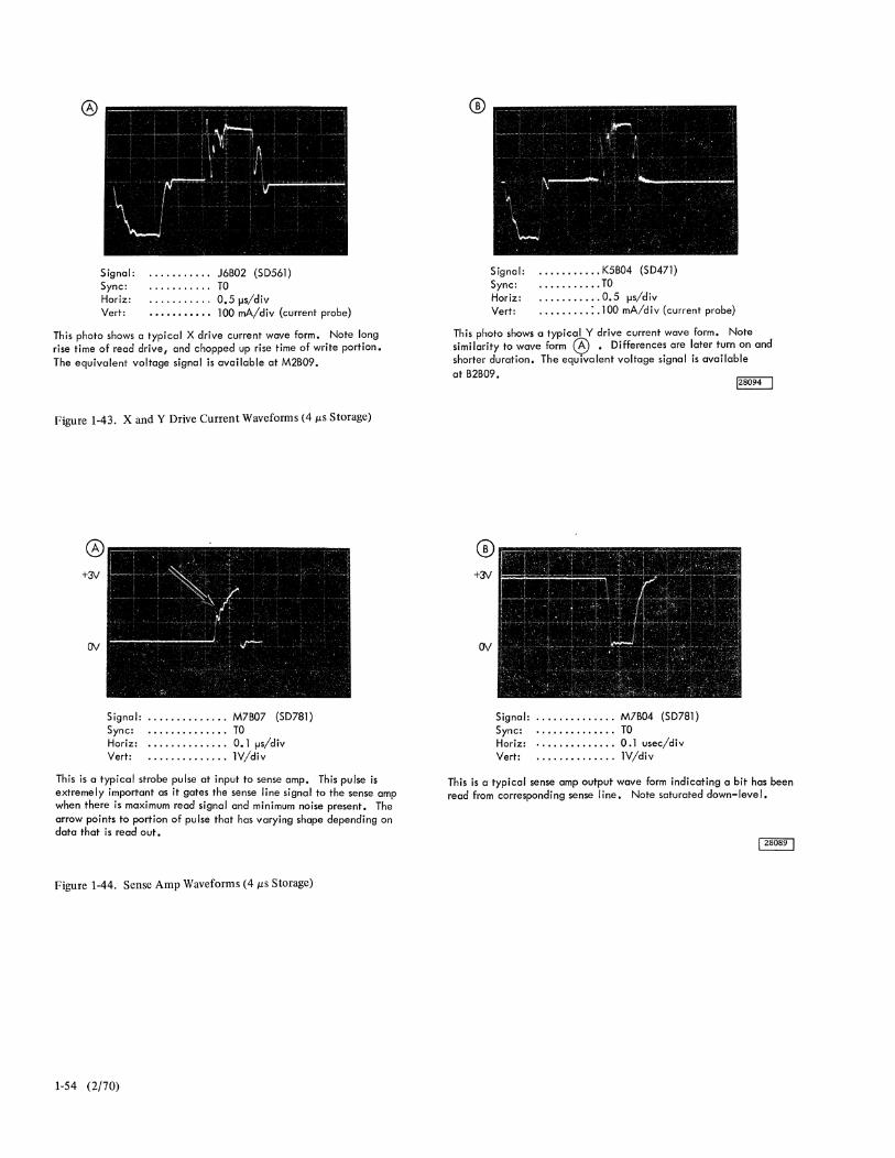
Signal: Sync: Horiz: Vert:
J6B02 (SDS61) TO O.S fJs/div 100 mA/div (current probe)
This photo shows a typical X drive current wave form. Note long rise time of read drive, and chopped up rise time of write portion. The equivalent voltage signal is available at M2B09.
Figure 1-43. X and Y Drive Current Waveforms (4 j.lS Storage)
Signal: Sync: Horiz: Vert:
M7B07 (SD781) TO 0.1 fJs/div lV/div
This is a typical strobe pulse at input to sense amp. This pulse is extremely important as it gates the sense line signal to the sense amp when there is maximum read signal and minimum noise present. The arrow points to portion of pulse that has varying shape depending on data that is read out.
Figure 1-44. Sense Amp Waveforms (4 j.lS Storage)
1-54 (2{70)
®
Signal: ..•..•..... KSB04 (SD471) Sync: Horiz:
........... TO
......•.•.. O.S fJs/div Vert: ..•....•. : .100 mA/div (current probe)
This photo shows a typical Y drive current wave form. Note similarity to wave form ® . Differences are later turn on and shorter duration. The equivalent voltage signal is available at B2B09.
Signal: Sync: Horiz: Vert:
M1B04 (SD781) TO 0.1 usec/div lV/div
This is a typical sense amp output wave farm indicating a bit has been read from correspondi ng sense Ii ne. Note saturated down-Ieve I.
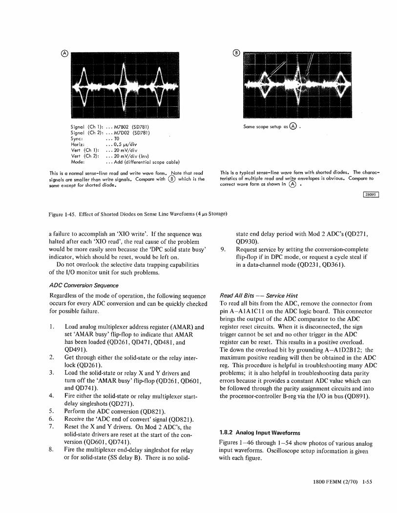
®
Signal Signal Sync:
(Ch 1): ... M7B02 (SD781) (Ch 2): ... M7D02 (SD781)
Horiz: Vert (Ch 1): Vert (Ch 2): Made:
••• TO ... 0.5 flS/div ... 20 mV/div ... 20 mV/div (Inv) ... Add (differential scope cable)
This is a normal sense-line read and write wave form. Note that read signals are smaller than write signals. Compare with ® which is the same except for shorted diode.
®
Same scope setup as (6) .
This is a typical sense-line wave form with shorted diodes. The characteristics of multiple read and write envelopes is obvious. Compare to correct wave form as shown in @ .
Figure 1-45. Effect of Shorted Diodes on Sense Line Waveforms (4 ILS Storage)
a failure to accomplish an 'XIO write'. If the sequence was halted after each 'XlO read', the real cause of the problem would be more easily seen because the 'DPC solid state busy' indicator, which should be reset, would be left on.
Do not overlook the selective data trapping capabilities of the I/O monitor unit for such problems.
ADC Conversion Sequence
Regardless of the mode of operation, the following sequence occurs for every ADC conversion and can be quickly checked for possible failure.
I. Load analog multiplexer address register (AMAR) and set 'AMAR busy' flip-flop to indicate that AMAR has been loaded (QD261, QD471, QD481, and QD49 I).
2. Get through either the solid-state or the relay interlock (QD261).
3. Load the solid-state or relay X and Y drivers and turn off the 'AMAR busy' flip-flop (QD261, QD601, and QD741).
4. Fire either the solid-state or relay multiplexer start-delay singleshots (QD271).
5. Perform the ADC conversion (QD821). 6. Receive the 'ADC end of convert' signal (QD82I). 7. Reset the X and Y drivers. On Mod 2 ADC's, the
solid-state drivers are reset at the start of the conversion (QD601, QD741).
8. Fire the multiplexer end-delay singleshot for relay or for solid-state (SS delay B). There is no solid-
9.
state end delay period with Mod 2 ADC's (QD271 , QD930). Request service by setting the conversion-complete flip-flop if in DPC mode, or request a cycle steal if in a data-channel mode (QD231, QD361).
Read All Bits -- Service Hint To read all bits from the ADC, remove the connector from pin A-AIAICII on the ADC logic board. This connector brings the output of the ADC comparator to the ADC register reset circuits. When it is disconnected, the sign trigger cannot be set and no other trigger in the ADC register can be reset. This results in a positive overload. Tie down the overload bit by grounding A-AID2BI2; the maximum positive reading will then be obtained in the ADC reg. This procedure is helpful in troubleshooting many ADC problems; it is also helpful in troubleshooting data parity errors because it provides a constant ADC value which can be followed through the parity assignment circuits and into the processor-controller B-reg via the I/O in bus (QD891).
1.8.2 Analog Input Waveforms
Figures 1-46 through 1-54 show photos of various analog input waveforms. Oscilloscope setup information is given with each figure.
1800 FEMM (2/70) 1-55
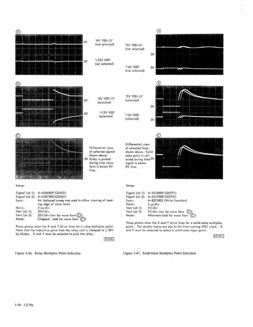
Setup:
Signal (ch I): Signal (ch 2): Sync:
Horiz: Vert (ch I): Vert (ch 2): Mode:
A-A2B6B09 (QD631) A-A2B7B08 (QD601)
OV
OV
OV
OV
'OV YOO-IS' (not se lected)
'+12V XOO' (not se lected)
'OV YOO-IS' (selected)
'+12V XOO' (selected)
Different io I vi ew of se lected signals shown above.
OV Relay is picked during time wave form is below OV line.
Int (delayed sweep was used to allow viewing of leading edge of wave form) 2 ms/div 20V/div 20V/div (inv for wave form ©) Chopped (add for wave form ©)
These photos show the X and Y drive lines for a relay multiplex point. Note that the inductive spike from the relay coil is clamped to ± 30V by diodes. X and Y must be selected to pick the relay.
Figure 1-46. Relay MUltiplex Point Selection
1-56 (2/10)
@
'OV YOO-IS' (not selected)
OV
'+6V XOO' OV (not se lected)
'OV YOO-IS' (selected)
OV
'+6V XOO' (selected) OV
Differential view of selected lines shown above. Solid state point is selected during time OV signal is below OV line.
Setup:
Signal (ch I): Signal (ch 2): Sync: Horiz: Vert (ch I): Vert (ch 2): Mode:
A-A2J6B09 (Q D771) A-A2J7B08 (QD741) A-B2F3B02 (Write Function) S ~s/div SV/div SV/div (inv for wave form ©) Alternate (add for wave form ©)
These photos show the X and Y drive lines for a solid-state multiplex point. The double traces are due to the free-running ADC clock. X and Y must be selected to select a solid-state input point.
Figure 1-47. Solid-State Multiplex Point Selection
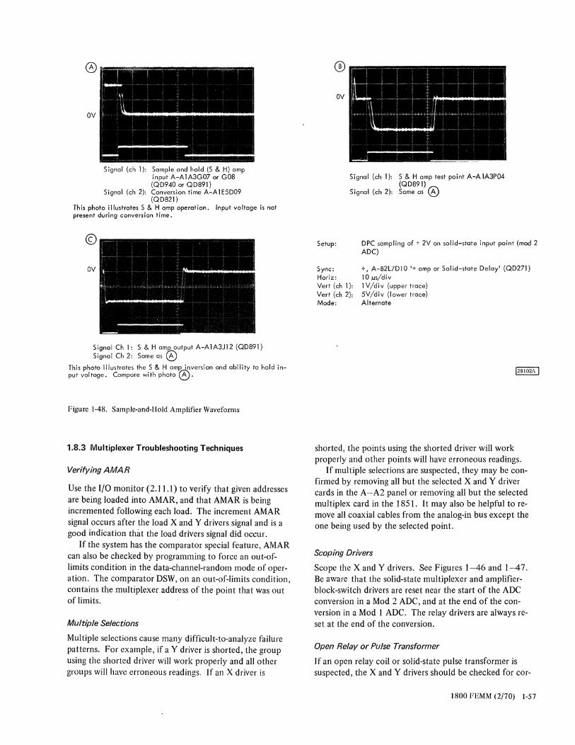
Signal (ch 1): Sample and hold (S & H) amp input A-AIA3G07 or GOS (QD940 or QDS91)
Signal (ch 2): Conversion time A-AIE5D09 (QDS21)
This photo illustrates S & H amp operation. Input voltage is not present during conversion time.
©
OV
Signal Ch I: S & H am~utputA-AIA3JI2 (QDS91) Signal Ch 2: Same as ®
This photo illustrates the S & H am~version and ability to hold input voltage. Compare with photo~.
Figure 1-48. Sample-and-Hold Amplifier Waveforms
1.8.3 Multiplexer Troubleshooting Techniques
Verifying AMAR
Use the I/O monitor (2.11. 1) to verify that given addresses are being loaded into AMAR, and that AMAR is being incremented following each load. The increment AMAR signal occurs after the load X and Y drivers signal and is a good indication that the load drivers signal did occur.
If the system has the comparator special feature, AMAR can also be checked by programming to force an out-oflimits condition in the data-channel-random mode of operation. The comparator DSW, on an out-of-limits condition, contains the multiplexer address of the point that was out of limits.
Multiple Selections
Multiple selections cause many difficult-to-analyze failure patterns. For example, if a Y driver is shorted, the group using the shorted driver will work properly and all other groups will have erroneous readings. If an X driver is
®
OV
Setup:
Sync: Horiz:
Signal (ch I): S & H amp test point A-A IA3P04 (QDS91) fA\
Signal (ch 2): Same as 0.J
DPC sampling of + 2V on solid-state input point (mad 2 ADC)
+, A-B2L7DIO ,+ amp or Solid-state Delay' (QD27J) IO.us/div
Vert {ch I}: 1 V/div (upper trace) 5V/div {lower trace} Alternate
Vert (ch 2): Mode:
shorted, the points using the shorted driver will work properly and other points will have erroneous readings.
If multiple selections are suspected, they may be confirmed by removing all but the selected X and Y driver cards in the A-A2 panel or removing all but the selected multiplex card in the 1851. It may also be helpful to remove all coaxial cables from the analog-in bus except the one being used by the selected point.
Scoping Drivers
Scope the X and Y drivers. See Figures 1-46 and 1-47. Be aware that the solid-state multiplexer and amplifierblock-switch drivers are reset near the start of the ADC conversion in a Mod 2 ADC, and at the end of the conversion in a Mod 1 ADC. The relay drivers are always reset at the end of the conversion.
Open Relay or Pulse Transformer
If an open relay coil or solid-state pulse transformer is suspected, the X and Y drivers should be checked for cor-
1800 FEMM (2/70) 1-57
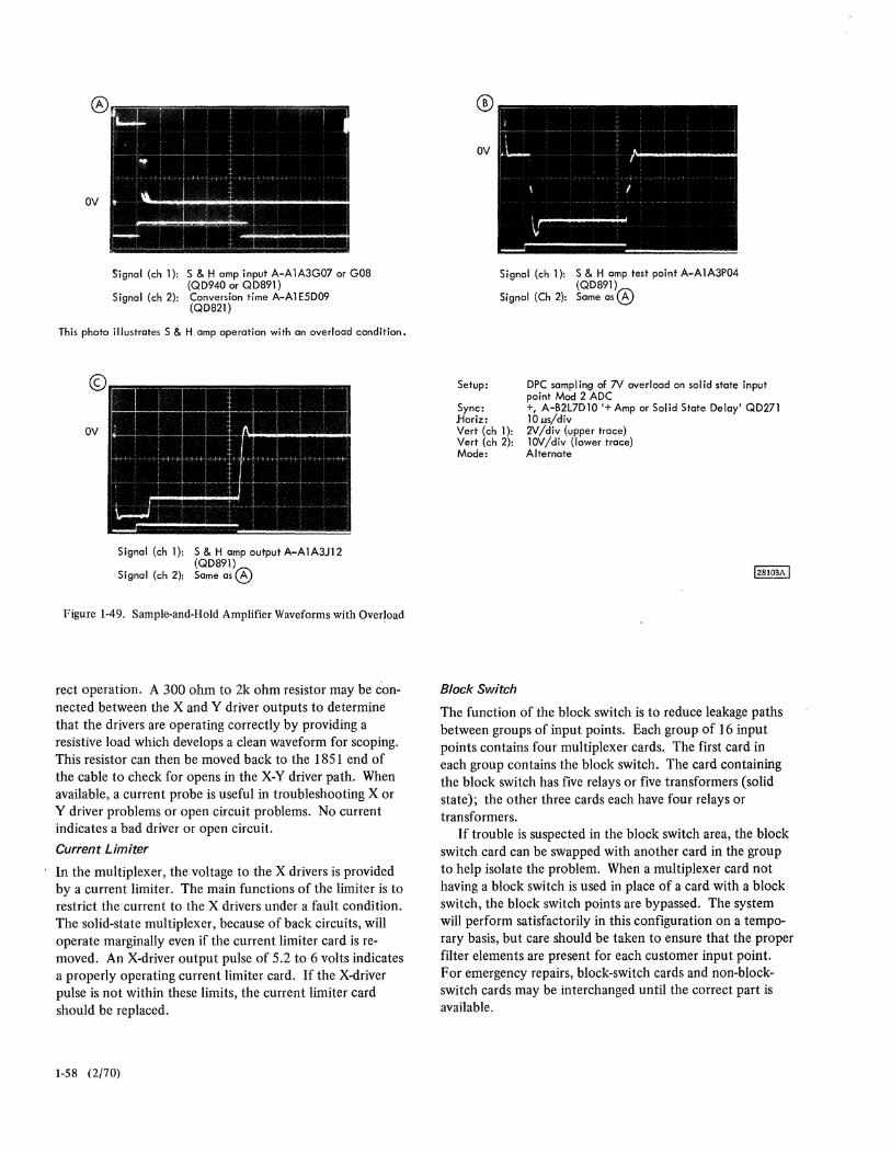
Signal {ch I}: S & H amp input A-AIA3G07 or GOS {QD940 or QDS91}
Signal {ch 2}: Conversion time A-AI E5D09 {QDS21}
This photo illustrates S & H amp operation with an overload condition.
Signal {ch I}: S & H amp output A-AIA3JI2 {QDS91}
Signal {ch 2}: Some as @
Figure 1-49. Sample-and-Hold Amplifier Waveforms with Over!oad
rect operation. A 300 ohm to 2k ohm resistor may be connected between the X and Y driver outputs to determine that the drivers are operating correctly by providing a resistive load which develops a clean waveform for scoping. This resistor can then be moved back to the 1851 end of the cable to check for opens in the X-Y driver path. When available, a current probe is useful in troubleshooting X or Y driver problems or open circuit problems. No current indicates a bad driver or open circuit.
Current Limiter
In the multiplexer, the voltage to the X drivers is provided by a current limiter. The main functions of the limiter is to restrict the current to the X drivers under a fault condition. The solid-state multiplexer, because of back circuits, will operate marginally even if the current limiter card is removed. An X-driver output pulse of 5.2 to 6 volts indicates a properly operating current limiter card. If the X-driver pulse is not within these limits, the current limiter card should be replaced.
I-58 (2/70)
Signal {ch I}: S & H amp test point A-AIA3P04 {QDS91}fi:\
Signal (Ch 2): Same as 0.;
Setup:
Sync: .Horiz: Vert (ch I): Vert (ch 2): Mode:
Block Switch
DPC sampling of 7V overload on solid state input point Mod 2 ADC +, A-B2L7DIO ,+ Amp or Solid State Delay' QD271 lOJ..ls/div 2V/div (vpper trace) IOV/div {lower trace} Alternate
The function of the block switch is to reduce leakage paths between groups of input points. Each group of 16 input points cont;,lins four multiplexer cards. The first card in each group contains the block switch. The card containing the block switch has five relays or five transformers (solid state); the other three cards each have four relays or transformers.
If trouble is suspected in the block switch area, the block switch card can be swapped with another card in the group to help isolate the problem. When a multiplexer card not having a block switch is used in place of a card with a block switch, the block switch points are bypassed. The system will perform satisfactorily in this configuration on a temporary basis, but care should be taken to ensure that the proper fIlter elements are present for each customer input point. For emergency repairs, block-switch cards and non-blockswitch cards may be interchanged until the correct part is available.
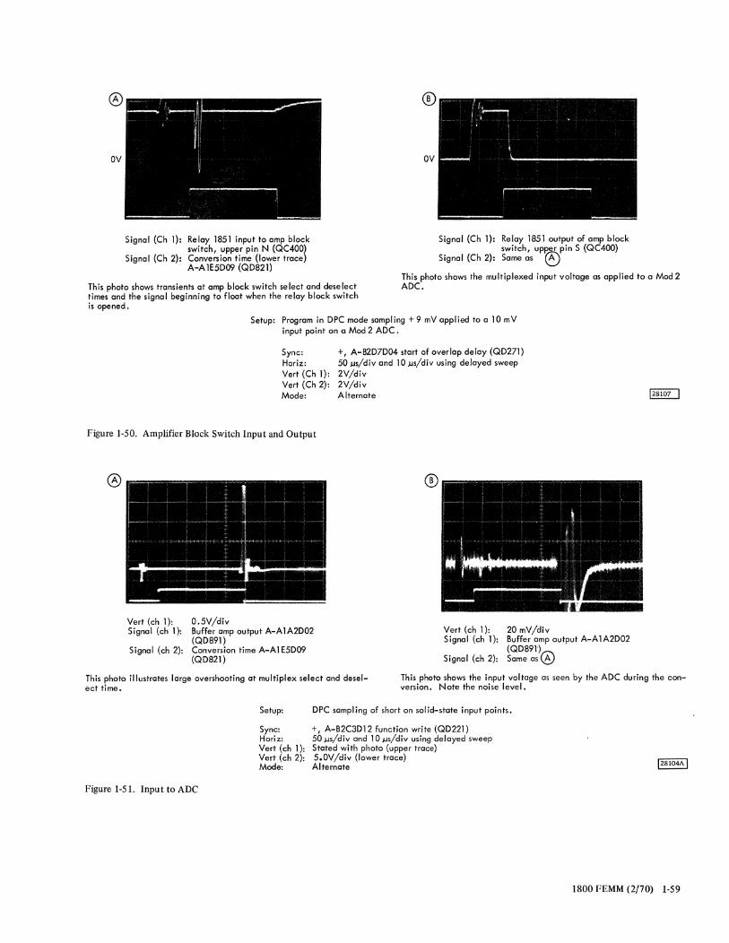
Signal (Ch 1):
Signal (Ch 2):
Relay 1851 input to amp block switch, upper pin N (QC400) Conversion time (lower trace) A-A lE5D09 (QD821)
®
OV
Signal (Ch 1): Relay 1851 output of amp block switch, up~pin S (QC400)
Signal (Ch 2): Sarne as 0J
This photo shows transients at amp block switch select and deselect tirnes ond the signal beginning to float when the relay block switch is opened.
ThIs photo shows the multiplexed input voltage as applied to a Mod 2 ADC.
Setup: Program in DPC mode sampling + 9 mV applied to a 10 mV input point on a Mod 2 ADC.
Sync: Horiz: Vert (Ch I): Vert (Ch 2): Mode:
+, A-B2D7D04 start of overlap delay (QD271) 50 )Js/div and 10 )Js/div using delayed sweep 2V/div 2V/div Alternate
Figure 1-50. Amplifier Block Switch Input and Output
Vert (ch 1): Signal (ch I):
Signal (ch 2):
0.5V/div Buffer amp output A-A1A2D02 (QD891) Conversion time A-A 1 E5D09 (QD821)
CD
Vert (ch 1): Signal (ch 1):
Signal (ch 2):
20 mV/div Buffer amp output A-A1A2D02 {QD891'}fA\ Same as.jy
This photo illustrates Idrge overshooting at multiplex select and deselecttime.
This photo shows the input voltage as seen by the ADC during the conversion. Note the noise level.
Setup:
Sync: Horiz: Vert {ch I}: Vert {ch 2}: Mode:
Figure 1-51. Input to ADC
DPC sampling of short on solid-state input points.
+, A-B2C3DI2 function write (QD221) 50 J,ls/dlv and 10 J,ls/div using delayed sweep Stated with photo (upper trace) 5.0V/div {lower trace} Alternate
1800 FEMM (2/70) 1-59
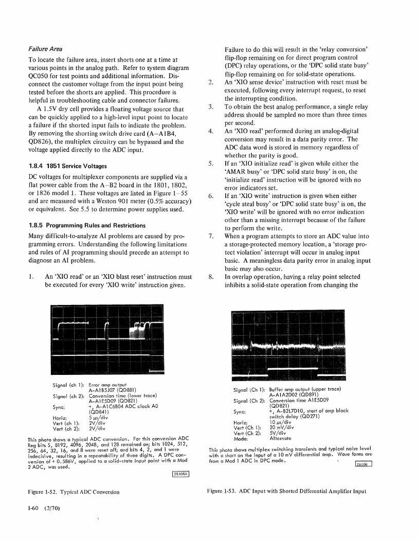
Failure Area
To locate the failure area, insert shorts one at a time at various points in the analog path. Refer to system diagram QC050 for test points and additional information. Disconnect the customer voltage from the input point being tested before the shorts are applied. This procedure is helpful in troubleshooting cable and connector failures.
A 1.5V dry cell provides a floating voltage source that can be quickly applied to a high-level input point to locate a failure if the shorted input fails to indicate the problem. By removing the shorting switch drive card (A-AIB4, QDS26), the mUltiplex circuitry can be bypassed and the voltage applied directly to the ADC input.
1.8.4 1851 Service Voltages
DC voltages for multiplexer components are supplied via a flat power cable from the A-B2 board in the IS01, IS02, or IS26 model 1. These voltages are listed in Figure 1-55 and are measured with a Weston 901 meter (0.5% accuracy) or equivalent. See 5.5 to determine power supplies used.
1.8.5 Programming Rules and Restrictions
Many difficult-to-analyze AI problems are caused by programming errors. Understanding the following limitations and rules of AI programming should precede an attempt to diagnose an AI problem.
1. An 'XIO read' or an 'XIO blast reset' instruction must be executed for every 'XIO write' instruction given.
Signal (ch 1):
Signal (ch 2):
Sync:
Horiz: Vert (ch 1): Vert (ch 2):
Error amp output A-A1B5J07 (QD881) Conversion time (lower trace) A-A 1 E5D09 (QD821) +, A-A1C6B04 ADC clock AO (QD841) 5 )..ls/div 2V/div 2V/div
This photo shows a typical ADC conversion. For this conversion ADC Reg bits S, 8192, 4096, 2048, and 128 remained oni bits 1024, 512, 256, 64, 32, 16, and 8 were reset Offi and bits 4, 2, and 1 were indecisive, resulting in a repeatability of three digits. A DPC conversion of+ 0.586V, applied to a solid-state input point with a Mod 2 ADC, was used.
Figure 1-52. Typical ADC Conversion
1-60 (2/70)
2.
3.
4.
5.
6.
7.
S.
Failure to do this will result in the 'relay conversion' flip-flop remaining on for direct program control (DPC) relay operations, or the 'DPC solid state busy' flip-flop remaining on for solid-state operations. An 'XIO sense device' instruction with reset must be executed, following every interrupt request, to reset the interrupting condition. To obtain the best analog performance, a single relay address should be sampled no more than three times per second. An 'XIO read' performed during an analog-digital conversion may result in a data parity error. The ADC data word is stored in memory regardless of whether the parity is good. If an 'XIO initialize read' is given while either the 'AMAR busy' or 'DPC solid state busy' is on, the 'initialize read' instruction will be ignored with no error indicators set. If an 'XIO write' instruction is given when either 'cycle steal busy' or 'DPC solid state busy' is on, the 'XIO write' will be ignored with no error indication other than a missing interrupt because of the failure to perform the write. When a program attempts to store an ADC value into a storage-protected memory location, a 'storage protect violation' interrupt will occur in analog input basic. A meaningless data parity error in analog input basic may also occur. In overlap operation, having a relay point selected inhibits a solid-state operation from changing the
Signal \ Ch 1):
Signal (Ch 2):
Sync:
Horiz: Vert (Ch 1): Vert (Ch 2): Mode:
Buffer amp output (upper trace) A-A1A2D02 (QD891) Conversion time A 1 E5D09 (QD821) +, A-B2L7D10, start of amp block switch delay (QD271) 10 }.Js/div 20 mV/div 5V/div Alternate
This photo shows multiplex switching transients and typical noise level with a short an the input of a 10 mV differential amp. Wave forms are from a Mad 1 ADC in DPC mode. r:::::-::::-l
I1hlQLJ
Figure 1-53. ADC Input with Shorted Differential Amplifier Input
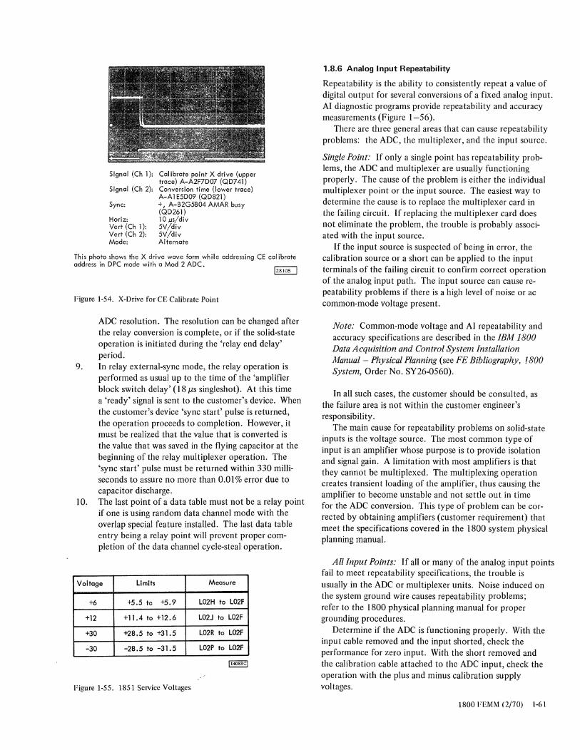
Signal (Ch I):
Signal (Ch 2):
Sync:
Horiz: Vert (Ch I): Vert (Ch 2): Mode:
Cal ibrate point X drive (upper trace) A-A2F7D07 (QD741) Conversion time (lower trace) A-A 1 E5D09 (QDB2l) +, A-B2GSB04 AMAR busy (QD26l) 10 Ms/div SV/div 5V/div Alternate
This photo shows the X drive wave form while addressing CE calibrate address in DPC mode with a Mod 2 ADC. 128105 1
Figure 1-54. X-Drive for CE Calibrate Point
ADC resolution. The resolution can be changed after the relay conversion is complete, or if the solid-state operation is initiated during the 'relay end delay' period.
9. In relay external-sync mode, the relay operation is performed as usual up to the time of the 'amplifier block switch delay' (18,us singleshot). At this time a 'ready' signal is sent to the customer's device. When the customer's device 'sync start' pulse is returned, the operation proceeds to completion. However, it must be realized that the value that is converted is the value that was saved in the flying capacitor at the beginning of the relay multiplexer operation. The 'sync start' pulse must be returned within 330 milliseconds to assure no more than 0.01% error due to capacitor discharge.
10. The last point of a data table must not be a relay point if one is using random data channel mode with the overlap special feature installed. The last data table entry being a relay point will prevent proper completion of the data channel cycle-steal operation.
Voltage Limits Measure
+6 +5.5 to +5.9 L02H to L02F
+12 +11.4 to +12.6 L02J to L02F
+30 +28.5 to +31.5 L02R to L02F
-30 -28.5 to -31.5 L02P to L02F
Figure 1-55. 1851 Service Voltages
1.8.6 Analog Input Repeatability
Repeatability is the ability to consistently repeat a value of digital output for several conversions of a fixed analog input. AI diagnostic programs provide repeatability and accuracy measurements (Figure 1-56).
There are three general areas that can cause repeatability problems: the ADC, the multiplexer, and the input source.
Single Point: If only a single point has repeatability problems, the ADC and multiplexer are usually functioning properly. The cause of the problem is either the individual multiplexer point or the input source. The easiest way to determine the cause is to replace the multiplexer card in the failing circuit. If replacing the multiplexer card does not eliminate the problem, the trouble is probably associated with the input source.
If the input source is suspected of being in error, the calibration source or a short can be applied to the input terminals of the failing circuit to confirm correct operation of the analog input path. The input source can cause repeatability problems if there is a high level of noise or ac common-mode voltage present.
Note: Common-mode voltage and AI repeatability and accuracy specifications are described in the IBM 1800 Data Acquisition and Control System Installation Manual- Physical Planning (see FE Bibliography, 1800 System, Order No. SY26-0560).
In all such cases, the customer should be consulted, as the failure area is not within the customer engineer's responsibility.
The main cause for repeatability problems on solid-state inputs is the voltage source. The most common type of input is an amplifier whose purpose is to provide isolation and signal gain. A limitation with most amplifiers is that they cannot be multiplexed. The mUltiplexing operation creates transient loading of the amplifier, thus causing the amplifier to become unstable and not settle out in time for the ADC conversion. This type of problem can be corrected by obtaining amplifiers (customer reqUirement) that meet the specifications covered in the 1800 system physical planning manual.
All Input Points: If all or many of the analog input points fail to meet repeatability speCifications, the trouble is usually in the ADC or multiplexer units. Noise induced on the system ground wire causes repeatability problems; refer to the 1800 physical planning manual for proper grounding procedures.
Determine if the ADC is functioning pro{lerly. With the input cable removed and the input shorted, check the performance for zero input. With the short removed and the calibration cable attached to the ADC input, check the operation with the plus and minus calibration supply voltages.
1800 FEMM (2/70) 1-61
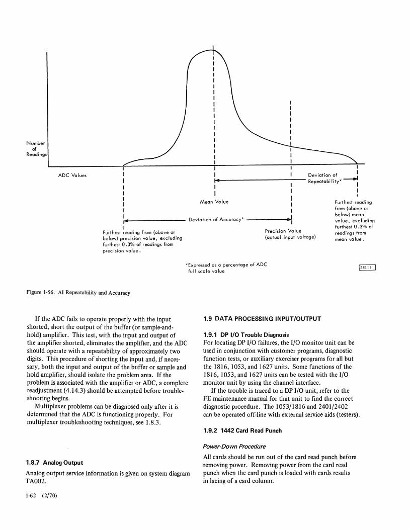
Number of
Readings
ADC Values
I D ., f 1 eVlatlon 0 -.....I
1"" .. 1-----------1-- Repeatabi lily* 1 1 I 1 1 1 I
Mean Va lue 1 Furthest reading 1 from (above or
141 I
below) mean Deviation of Accuracy* ------.. ~I value, excluding
Furthest reading from (above or below) precision value, excluding furthest 0.3% of readings from prec ision va lue .
Precision Value (actual input voltage)
furthest 0.3% of readings from mean value.
*Expressed as a percentage of ADC fu" sca Ie va lue
Figure 1-56. AI Repeatability and Accuracy
If the ADC fails to operate properly with the input shorted, short the output of the buffer (or sample-andhold) amplifier. This test, with the input and output of the amplifier shorted, eliminates the amplifier, and the ADC should operate with a repeatability of approximately two digits. This procedure of shorting the input and, if necessary, both the input and output of the buffer or sample and hold amplifier, should isolate the problem area. If the problem is associated with the amplifier or ADC, a complete readjustment (4.14.3) should be attempted before troubleshooting begins.
Multiplexer problems can be diagnosed only after it is determined that the ADC is functioning properly. For multiplexer troubleshooting techniques, see 1.8.3.
1.8.7 Analog Output
Analog output service information is given on system diagram TA002.
1-62 (2/70)
1.9 DATA PROCESSING INPUT/OUTPUT
1.9.1 DP I/O Trouble Diagnosis For locating DP I/O failures, the I/O monitor unit can be used in conjunction with customer programs, diagnostic function tests, or auxiliary exerciser programs for all but the 1816,1053, and 1627 units. Some functions of the 1816, 1053, and 1627 units can be tested with the I/O monitor unit by using the channel interface.
If the trouble is traced to a DP I/O unit, refer to the FE maintenance manual for that unit to find the correct diagnostic procedure. The 1053/1816 and 2401/2402 can be operated off-line with external service aids (testers).
1.9.2 1442 Card Read Punch
Power-Down Procedure
All cards should be run out of the card read punch before removing power. Removing power from the card read punch when the card punch is loaded with cards results in lacing of a card column.
Chapter 2. Console and Maintenance Features
2.1 PROGRAMMER'S CONSOLE
The programmer's console (Figure 2-1) provides the means for manual control of the processor-controller during troubleshooting or operating phases.
The basic operating features and controls provide the facility to:
1. Start or stop instruction execution. 2. Set up and store data or instructions. 3. Communicate with the program via sense and program
switches. 4. Indicate machine conditions and status. 5. Display core storage words and register data. 6. Write or clear storage-protect bits. 7. Initial program load. 8. Trace each instruction. 9. Interrupt the program manually. 10. Control the cycling rate by the run, single-storage-
cycle, single-instruction, or single-step mode. 11. Clear core storage. 12. Reset all control circuitry. 13. Turn power on and off.
2.1.1 Switches and Message Lamps
There are two rows of pushbutton switches and message lamps. One row is at the top of the console and one row is at the bottom.
Clear Storage
This pushbutton switch has four functions (Figure 2-2). However, none of the four functions can be executed until CLEAR STORAGE (CA1S1) is held pressed, then START is pressed. This dual action requirement prevents the accidental clearing of storage. Note in Figure 2-2 that each clear-storage function is dependent on the positions of the mode switch and the write-storage-protect-bits switch.
The P-C continuously cycles through all core storage addresses during the clear-storage operation.
Program Load
This pushbutton switch (CA1S1) is used to load an IPL card (1442) or IPL tape record (1054) into main or aUXiliary storage. The IPL card or tape record must contain instructions that will load the remaining cards or tape records, unless the entire program is contained in the IPL card or tape record. (See paragraph 2.2, "Initial Program Load.")
Ready
When on, this lamp (Y A141) indicates that power is supplied to all P-C circuits and that the P-C is ready to operate. This
lamp does not indicate the ready status of individual DP I/O units.
On
This pushbutton switch (Y A 140) is used to power-up the 1800 system. Pressing the on button starts the power-on sequence (1.7 seconds to ready condition) and generates a power-on reset signal.
Off
This pushbu tton switch (Y A 140) is used to power-down the 1800 system. Presssing the off button drops all power in the system with the exception of the 11S-Vac convenience outlets, the 24-Vac sequencing voltage, and line voltage at the 1053 Printer and 1816 Printer-Keyboard, which have their own power cords.
Power On
This lamp (Y A 141) is turned on when the on button is pressed. The lamp remains on to indicate that power is delivered to the P-C power supplies and blowers, and to external units that receive their power from the P-C.
Lamp Test
This pushbutton switch (CAl 5 1) is pressed to test the operation of all SCRID-actuated lamps (the small, round indicator lamps on the console).
Wait
When on, this lamp (CA1S1) indicates that the P-C is in either load or display mode, or that it has been halted by a 'wait' instruction.
Run
When on, this lamp (CAl 51 ) indicates that the P-C is operating under program control.
Alarm
This lamp (Y A 141) turns on to indicate that the operations monitor preselected time interval has expired. The lamp remains on until the operations-monitor switch is turned off.
Emergency Pull
This switch (YA140) is for emergency use only. If pulled off, all electrical power (except 24-Vac sequencing voltage) is immediately removed from all system units except the 1053 Printer and 1816 Printer-Keyboard, which have their own power cords.
1800 FEMM (2/70) 2-1
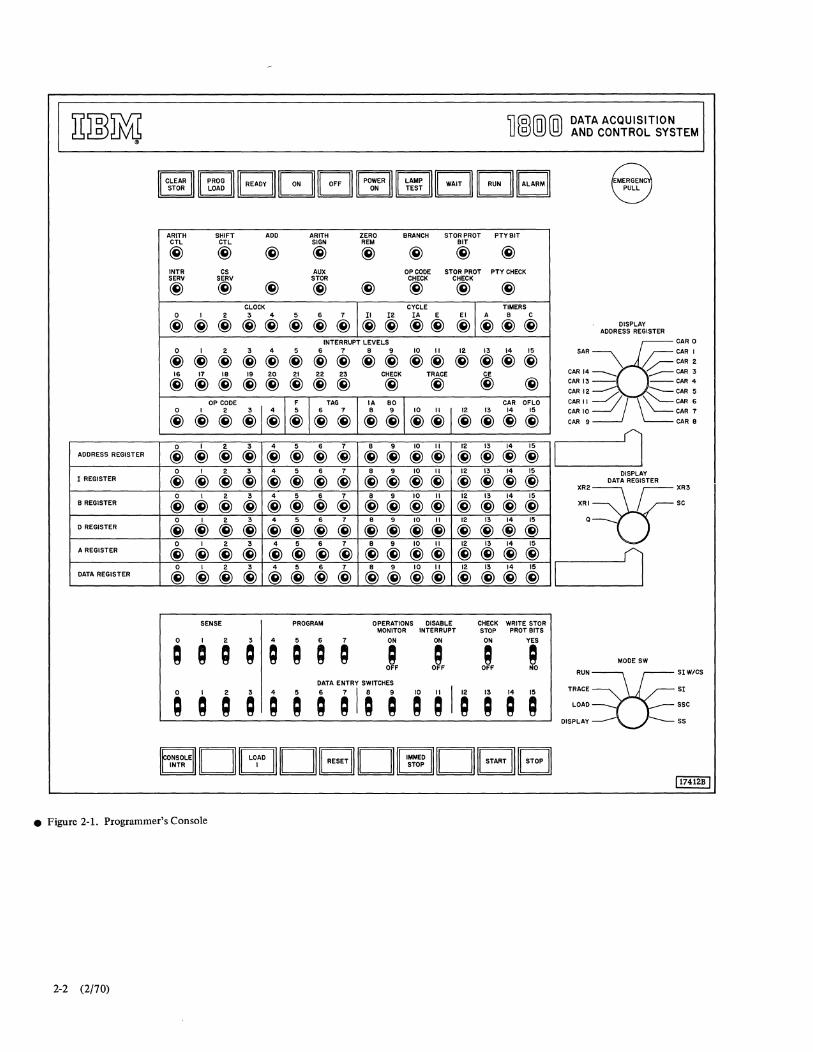
ARITH SHIFT ADD ARITH ZERO BRANCH STORPROT PTYBIT CTL CTL SIGN REM BIT
@ @ @ @ @ @ @ @ INTR CS AUX OPCODE STOR PROT PTY CHECK SERV SERV STOR CHECK CHECK
@ @ @ @ @ @ @ @ CLOCK CYCLE
@I@ TIMERS
0 I 2 3 4 5 6 7 II 12 IA E a C
@ @@ @@@ @@ @@ @@ @@ INTERRUPT LEVELS
0 I 2 3 4 5 6 7 8 9 10 " 12 13 14 15
@@ @ @@@ @@ @@ @@ @ @@@ 16 17 18 19 20 21 22 23 CHECK TRACE C~
@ @@ @@@@@ @ @ @ @ OP CODE
@ I@I~ I@TAG@
IA BO I
CAR OFLO 0 I 2 8 @@@I@@ 14 15
@ @@ @ @@ 0 I 2 3 4 5 6 7 8 9 10 " 12 13 14 15
ADDRESS REGISTER @ @@@ @@@ @ @@@@ @@@@ 0 I 2 3 4 5 6 7 8 9 10 " 12 13 14 15
I REGISTER @ @@@ @@@@ @@@@ @@@@ 0 I 2 3 4 5 6 7 a 9 10 " 12 13 14 15
a REGISTER @ @@ @ @@@@ @@@@ @@@@ 0 I 2 3 4 5 6 7 8 9 10 " 12 13 14 15
D REGISTER @ @@@ @@@@ @@@@ @@@@ 0 I 2 3 4 5 6 7 B 9 10 " 12 13 14 15
A REGISTER @ @@@ @@@@ @@@@ @@@@ 0 I 2 3 4 5 6 7 8 9 10 " 12 13 14 15
DATA REGISTER @ @@@ @@@@ @@@@ @@@@
SENSE PROGRAM OPERATIONS DISABLE CHECK WRITE STOR MONITOR INTERRUPT STOP PROT alTS
ON ON ON YES g ~ A g OFF OFF OFF NO
A A 6 6 ; 6 ; 6
6 ~ 6 6 ; 6 6TA ErriTCHEi i ~ Iii i i
[![]DBBJ • Figure 2-1. Programmer's Console
2-2 (2/70)
I
I
DATA ACQUISITION AND CONTROL SYSTEM
DISPLA y GISTER ADDRESS RE
SAR\ ~CARO
CAR I
'~CAR 2 / -CAR 3
--CAR 4
CAR 14 __
CAR 13--
CARI2=::/:
CARII""2j
CAR 5
'\ "--CAR 6
~CAR7 CAR 8
CAR 10
CAR 9
XR2
XRI
Q
I DISPLA y
STER DATA REGI
~XR3 --uK 1
MODE SW
RUN~SIW/CS TRACE SI
LOAD SSC
DISPLAY - - SS
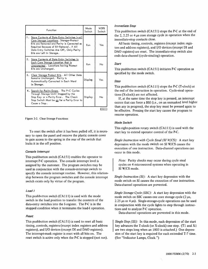
Function Mode WSPB
Switch Switch
1. Store Contents of Data Entry Switches in all Core Starage Locations. Storage-Protect Bits are Removed and Parity is Corrected as
Run Yes Required Because of Bit Removal. If All Data Entry Switches Are Off I Only Parity Bits are Left in Storage.
2. Store Contents of Data Entry' Switches in Each Core Storage Location that is
Run No UnP.fotected. Locations having Protect Bits are Unchanged.
3. Clear Storage Protect Bits. All Other Data Remains Unchanged. Parity is
Disp Icty Yes Automatically Corrected in Each Word in Storage.
4. Search for Pari ty. Errors. The P-C Cycles Through Storage Unti I Stopped by the Stop Key or a Parity Error. The Check Display No Stop Swi tch Must be ~ for a Pari ty Error to Cause a Stop.
Figure 2-2. Clear Storage Functions
To reset the switch after it has been pulled off, it is necessary to open the panel and remove the plastic console cover to gain access to the spring in the rear of the switch that locks it in the off position.
Console Interrupt
This pushbutton switch (CAl 51) enables the operator to interrupt P-C operation. The console interrupt level is assigned by the customer. The program switches may be used in conjunction with the console-interrupt switch to specify the console interrupt routine. However, this relationship between the program switches and the console interrupt switch exists only by virtue of the program.
Load I
This pushbntton switch (CAllI) is used with the mode switch in the load position to transfer the contents of the data-entry switches into the I-register. The P-C is in the stopped condition when it terminates the load-I operation.
Reset
This pushbutton switch (CAI51) is used to reset all basic timing, controls, registers (except index registers and address registers), and I/O devices (except DI and DAO registers). The interrupt-mask register is reset with all bits on. The reset switch is active only when the P-C is stopped (not run).
Immediate Stop
This pushbutton switch (CAI51) stops the P-C at the end of the 2, 2.25 or 4 J1S core storage cycle in operation when the immediate-stop contacts close.
All basic timing, controls, registers (except index registers and address registers), and I/O devices (except DI and DAO registers) are reset. The immediate-stop switch also ends data-channel (cycle-stealing) operation.
Start
This pushbutton switch (CAl 51 ) initiates P-C operation as specified by the mode switch.
Stop
This pushbutton switch (CAllI) stops the P-C (T-clock) at the end of the instruction in operation. Cycle-steal operations (X-clock) are not affected.
If, at the same time the stop key is pressed, an interrupt occurs that can force a BSI (i.e., on an unmasked level higher than any in progress), the stop key must be pressed again to be effective. Pressing the start key causes the program to resume operation.
Mode Switch
This eight-position rotary switch (CAllI) is used with the start key to extend operator control of the P-C.
Single Instruction with Cycle Steal (Sf W/CS): A start key depression with the mode switch on SI W/CS causes the execution of one instruction. Data-channel operations can occur in this mode.
Note: Parity checks may occur during cycle steal cycles on 4 microsecond systems when operating in SI W/CS mode.
Single Instruction (SI): A start key depression with the mode switch on SI causes the execution of one instruction. Data-channel operations are prevented.
Single Storage Cycle (SSC): A start key depression with the mode switch on SSC causes one core storage cycle (2 J1S, 2.25 J1S or 4 J1s). Single-storage-cycle operations can be used in conjunction with the cycle lights to step through instructions and to analyze P-C operation.
Data-channel operations are prevented in this mode.
Single Step (SS): In this mode, each depression of the start key advances the T-clock (or X-clock) one step. (Tl and Xl are two steps long when an 1803 is attached.) One depression of the start key is reqUired for each extended T-7 time. (See "Indicator Lamps, Clock.")
1800 FEMM (2/70) 2-3
Once single-stepping has begun, the clock cycle should be stepped past T4 or X4 time before pressing the reset key or switching out of SS mode.
The SS mode is normally used with direct program control. This mode can be used with data channel operations; however, data overruns can usually be expected.
Run: A start key depression with the mode switch on run initiates normal program operation of the P-C.
Trace: This position of the mode switch causes a trace interrupt after the execution of each instruction (except XIO).
The trace interrupt is a unique interrupt. It has no device status word and no interrupt level status word, and it cannot be masked. The trace interrupt is the lowest priority customer interrupt. Once initiated, it is delayed by the occurrence of any other interrupt. It cannot occur while other interrupts are being serviced. When the trace interrupt occurs, the P-C executes the forced BSI and branches to the routine whose address is stored at /0009.
Data-channel operations can occur in trace mode.
Load: A start key depression with the mode switch on load causes the contents of the data-entry switches to be stored at the address specified by the I-register. (The P-C must be in a stopped condition.) The I-register is incremented following each load operation caused by pressing the start key.
A load-I key depression with the mode switch on load causes the contents of the data-entry switches to be stored in the I-register.
Data-channel operations are prevented in load mode.
Display: A start key depression with the mode switch on display causes the data at the I-register address to be displayed in the console B-register lights. The I-register is incremented after each display. Successive words are displayed with successive depressions of the start key.
Data-channel operations are prevented in display mode.
2.1.2 Toggle Switches
Sense and Program
The contents of these eight switches (CA22I) may be stored in bit positions 0-7 of the A-register or a COre storage location. An XIO instruction with a function of 'read' stores the contents of the sense and program switches at the core storage address specified by the 10CC. A function of 'sense device' stores the switch data in the A-register.
Operations Monitor
. This switch (CAISI) is used to start the operations monitor. The off position disables the operations monitor.
2-4 (2/10)
Disable Interrupt
This switch (CAIS 1) is used to suspend all interrupts, including internal errors. While the switch is on, any interrupt that is not masked will latch its 'level' flip-flop in the normal manner, but the active output of the flip-flop will be inhibited. When the switch is turned off, the latched interrupts will be serviced on a priority basis.
Check Stop
When the check-stop switch (CAISI) is on, the P-C program will be stopped by any of the follOWing internal errors: invalid operation, B-reg parity error, or storage-protect violation. Each of these errors turns on an associated indicator (red lamp) on the console.
The stop occurs at the end of the core storage cycle in which the error is detected. All operations, including cyclestealing, are suspended during the check-stop. START must be pressed to restart the system; reset is not necessary. (A check-stop can also be activated via the I/O channel wired interface when the I/O monitor unit is used to trap data. See paragraph 2.11.1.)
The check-stop switch can be used during a clear-storage operation to stop the P-C if a B-reg parity error is detected. (See Figure 2-2.)
When the check-stop switch is off, and the disable-interrupt switch is off, an internal error will cause an internallevel interrupt except on data transfer cycles. (See Figure 1-20.) The P-C program continues to run, and the internal ILSW indicates to the program the cause of the interrupt.
Note in Figure 1-20 that the check-stop switch has no control over the functions of a CAR-check error.
Write Storage Protect Bits
This switch (CAl S 1) enables the writing or clearing of storage-protect bits using the 'store status' instruction or the clear-storage pushbutton (Figure 2-2). This switch must not be operated while the P-C is running or a parity error may result.
Data Entry Switches
The contents of these 16 toggle switches (CA2II) can be stored by either manual or program control. Manual control is described under "Mode Switch, Load." Program control requires an XIO (area 0), 'read' or 'sense device' instruction (Figure 1-13, Part 1).
2.1.3 I ndicator Lamps
These lamps show the status of significant controls and indicators in the P-C.
Arithmetic Control (ARITH CTL)
On during arithmetic operations (CB511), including effective address generation. Driven by 'arithmetic control' flip-flop.
Shift Control (SHIFT CTL)
On during shift operations (CB511).
Add
On during add operations (CB511). Driven by 'add' flipflop. Subtract operations are indicated by the ARITH CTL lamp being on and the add lamp being off.
Arithmetic Sign (ARITH SIGN)
On when bit position 0 in the A-register does not initially equal bit position 0 in the B-register (CB511).
Zero Remainder (ZERO REM)
On when the A-register contains a zero balance during a divide operation (CB511).
Branch
On during extended T7 time of a branch instruction (CB511).
Storage Protect Bit (STOR PROT BIT)
On when a storage-protect bit is transferred with the 16 data bits between the B-register and core storage (CB511).
Parity Bit (PTY BIT)
On when a parity bit is transferred with the 16 data bits between the B-Register and core storage (CB511).
Interrupt Service (lNTR SERV)
Turned on when any interrupt level is active (CB521).
Cycle Steal Service (CS SERV)
On when any cycle-steal level is active (CB521).
Auxiliary Storage (AUX STOR)
On when auxiliary storage is being used (CB521).
Op Code Check
Turned on when an invalid op code is placed in the op register. The op-code-check indicator (CB521) is turned off and the check indicator is turned on (internal interrupt) at the end of the cycle in which the error is sensed, allowing the op-code-check indicator to indicate any subsequent error.
Storage Protect Check (STOR PROT CHECK)
Turned on when an attempt is made to write into a storageprotected location, except location /OOOA in conjunction with a CE interrupt, or locations /0004, /0005, and /0006 during interval timer updating.
The storage-protect-check indicator (CB521) is turned off and the check indicator is turned on (internal interrupt) at the end of the cycle in which the error is sensed. This is to allow the storage-protect-check indicator to indicate any subsequent storage-protect error.
Parity Check (PTY CHECK)
Turned on when a parity error (even number of bits) is detected in the 18-bit word transfer between the B-register and core storage. The presence or absence of storage-protect and parity bits in each word is indicated by their respective console indicators.
The parity-check console indicator (CB521) is turned off and the check indicator is turned on (internal interrupt) at the end of the cycle in which the error is sensed, allowing the parity-check indicator to indicate any subsequent parity error.
Clock
These eight lamps (0-7, shown on CB631) indicate the status of the T-clock or X-clock. Normally used during start-key depreSSions when the mode switch is on single-step (SS).
Cycle
These five lamps (II, 12, lA, E, and El, shown on CB651) indicate the progress of an instruction that is being singlestepped (SS mode) or single-cycled (SSC mode).
Timers
These three lamps (A, B, and C, shown on CB651) indicate the status of their respective interval timers. An on condition indicates that the timer is in operation.
Interrupt Levels
An interrupt-level indicator (CB681) is turned on for each interrupt level requesting service or being serviced. Once on, an interrupt-level indicator can be reset by either of two instructions:
1. A 'mask' instruction that is executed before servicing of the interrupt begins. (The interrupt request is not lost but merely detained until the interrupt level is unmasked, at which time the indicator is turned back on. The only exception to this is 'programmed interrupt.')
2. A 'branch out of interrupt' (BOSC) instruction is executed to complete servicing of the interrupt.
Both of the above instructions are quasi-instructions; that is, they are variations of the XIO and BSC instructions.
The last three interrupt-level indicators - CE, trace, and check (internal interrupt) - cannot be masked. The CE interrupt (2.7) can be initiated only from the P-C monitor interface panel or from a device operating in CE mode.
1800 FEMM (2/70) 2-5

Operation Code (OP CODE)
These five lamps (0-4, shown on CB751) display the op code of each instruction.
Format (F)
On when a two-word instruction is specified (CB751).
Tag
These two lamps indicate the register (XR-1, XR-2, XR-3, or I-register) specified in the instruction. (See Figures 1-1 1-2 and page CB751.)
Indirect Addressing (fA)
On when there is a bit in position 8 of the long-format instruction, which indicates indirect addressing. (See Figure 1-2 and page CB751.)
Branch Out (BO)
On when there is a bit in position 9 of the instruction. In a BSC instruction, this bit specifies a 'branch out of interrupt' (BOSC). (See Figure 1-2 and page CB751.)
Carry (CAR)
On when there is a carry condition in the A-register (CB751).
Overflow (OFLO)
On when an overflow occurs in the A-register (CB751).
2.1.4 Register Display Lamps and Switches
Six rows of indicators and two rotary switches facilitate the display of data registers in the P-C.
Address Register
These 16 lamps (CB781) display the contents of the storageaddress register (M-register) or one of the channel-address registers, depending on the position of the display-address rotary switch. The selected register is displayed each time the P-C comes to a stop or wait condition.
Note: Under certain conditions, a channel address register may be displayed while the display-address rotary switch is in the SAR position. See 'Effect of Cycle-Stealing on SAR Display Lamps" (1.7.1).
Display Address Register Switch
This 10- or 16-position rotary switch (CAllI) is used to select the storage-address register (M-register) or a channeladdress register for display in the address-register lamps.
2-6 (2/70)
Permanent Register Displays: I (CB821), B (CB861), D (CB-901), and A (CB941)
The contents of these four registers are always displayed.
Data Register
These 16 lamps (CB981) are driven directly from the A-register-in bus. Each time the P-C is stopped at the end of a cycle (T-7 end-op or X-7 time), the lamps display the contents of the register selected by the display-data register rotary switch. In single-step mode, the lamps display the data that is present on the A-register in bus at each step of the cycle in progress.
Display Data Register Switch
This five-position rotary switch (CAlli) is used to select the Q-register, an index register, or the shift counter for display in the data-register lamps. (See "Data Register.")
2.2 INITIAL PROGRAM LOAD (IPL)
In the 1800 system, the first 1442 Card Read Punch is always wired as the IPL device. If there is no 1442 in the system, the 1054 Paper Tape Reader is wired as the IPL device.
The IPL program can be loaded into either main storage or auxiliary storage, depending upon the position of the forceauxiliary switch on the P-C monitor interface panel (2.5.2).
2.2.1 1442 Standard IPL Procedure
When the 1442 is used for initial program load, it operates in packed mode, reading the 80 columns of the first card into the first 40 core storage locations (/0000/0027). Each core storage location stores the binary data from two card columns. For example, binary data from card column I (rows 12-5) is read into bit positions 8-15 or core storage location /0000 and binary data from card column 2 (rows 12-5) is read into bit positions 0-7 of the same core storage location. Rows 6-9 of the card are not read into core storage.
The remainder of the first card is entered in the same manner, entering all odd numbered card columns into bit positions 8-15 of their respective core storage locations, and entering all even numbered card columns into bit positions 0-7 of their respective core storage locations.
1.
2. 3.
Place program deck in 1442 hopper and press 1442 start key to cause a run-in cycle. Press RESET on P-C console. Set console mode switch to RUN (or SI W/CS) and press PROGRAM LOAD.
After the first card is read into core storage, the P-C begins (at /0000) executing the instructions that were stored from the first card if in run mode. The first card must contain instructions to load the remainder of the program cards.
2.2.2 1054 Standard IPl Procedure
When the 1054 Paper Tape Reader is used for initial program load, tape data is loaded into core storage, starting at location /0000 and loading successively higher core storage locations until an end-of-record punch is sensed in the tape. Each core storage location stores the binary data from four tape characters. For example, binary data from the first tape character (channels 4-1) is stored in bit positions 0-3 of core storage location /0000 and binary data from the fourth tape character (channels 4-1) is stored in bit positions 12-15 of core storage location /0000. Channels 5-8 of the paper tape are not loaded into core storage during initial program load.
The remainder of the tape data is entered in the same manner (four characters per word) until a channel-5 punch is sensed (any channel-5 punch except when it is in a delete character). The channel-5 punch is the end-of-record character and is not read into core storage. An entire program may be loaded from paper tape in IPL mode.
Interrupt requests from the 1054 are suppressed while in IPLmode.
1. Load IPL tape. 2. Press RESET on P-C console. 3. Set console mode switch to RUN and press PRO
GRAM LOAD.
After the IPL tape record is read into core storage, the P-C begins (at /0000) executing the instructions that were stored in IPL mode. If the entire program was not included in the IPL tape record, the IPL record must contain instructions for loading the remainder of the tape records (program).
2.2.3 IPl into Any Core location
In IPL mode, the I-register setting specifies the starting address for the program-load operation. When the console reset key is pressed, the I-register is reset to address /0000. However, the contents of the I-register can be set to any desired starting address before loading the program. This choice of starting address makes it possible to load a small program, one that uses displacement addressing exclusively, into an area of core storage without disturbing the contents of the normal IPL area.
Method 1 -- Loading But Not Executing the Program
1. Insert IPL-type program into IPL device and ready device.
2. Press RESET on P-C console. 3. Set I-register to desired load address. 4. Set console mode switch to SI and press PROGRAM
LOAD. The program will IPL into the location specified by the I-register and then will stop.
Method 2 -- Loading and Executing the Program
1. Insert IPL-type program into IPL device and ready device.
2. Record contents of core locations /0000 and /0001, then load /4COO into location /0000.
3. Load desired IPL load address into location /0001. 4. Press RESET on P-C console. 5. Set I-register to desired load address. 6. Set console mode switch to RUN and press PROGRAM
LOAD. The program will IPL into the location specified by the I-register and then will branch to /0000 for its first instruction, which is a BSC to the loaded program whose address is in location 0001.
7. Restore contents oflocations /0000 and /0001 recorded in step 2.
2.3 ERROR CHECK CIRCUITS
Within the processor-controller, all data is parity checked as it is written from the B-reg to storage. The P-C also checks for invalid operation codes appearing in the op-code register, and it checks for an attempt to write into a storage-protected position of core storage.
Channel address register (CAR) checking is provided to ensure that the first word addressed by a selected CAR is the first word of the correct data table.
A CAR check is made for all devices after the address from the IOCC word is transferred to the selected CAR. During the E2 data cycle, a bit-by-bit comparison is made between the contents of the selected CAR (channel address bus) and the contents of the B-register (channel data bus). If any of the corresponding bits are not equal, a CAR check error has occurred. This E2-cycle CAR check error terminates subsequent cycle-steal requests for the assigned I/O device and initiates an internal interrupt. The I/O device cannot request a cycle steal until the interrupt level status word for the internal interrupt is sensed and the I/O device is reinitialized by another XIO instruction.
Another CAR check is made for chaining each time the I/O device chains to a different data table. The CAR check at the beginning of the second data table and all subsequent data tables in the chain is accomplished as follows: The first word of the data table (second data table, third data table, etc.) must contain its own address. After the first word of the data table is addressed and loaded into the B-register, a bit-by-bit comparison is made between the contents of the selected CAR (channel address bus) and the contents of the B-register (channel data bus). If any of the. corresponding bits are not equal, a chaining CAR check error has occurred. Subsequent cycle-steal requests are terminated and a bit is set in the DSW of the device.
The action taken by the processor-controller when an internal error is detected depends on the type of error and the position of the check-stop switch. (See Figure 1-20).
1800 FEMM (2/70) 2-7
The B-reg parity error, storage-protect violation, and CAR-check error are sent to each I/O adapter via the out bus. If one of these errors occurs while a device is selected, the I/O adapter may take one or more of the following actions:
1. Initialize a device interrupt. 2. Reject the command. 3. Ignore the data. 4. Indicate the error in the device status word.
The I/O adapters also contain checking circuits. The outputs of these circuits are the sensed indicators which make up the device status word. The DSW, through proper programming, can be used to identify the type of error and to guide corrective action in the operating program. The DSW can also be used to log errors during customer run time for later analysis by the customer engineer.
The device status word indicates three types of information: (1) error or exception interrupts, (2) normal data or service interrupts, and (3) routine status. By means of the I/O monitor (2.11.1) these signals can be displayed and identified.
Error check analysis diagrams (ECAD) are provided in the maintenance diagram manual to assist in tracing errors to their source.
2.4 MAINTENANCE DIAGNOSTIC PROGRAMS
The maintenance program system was developed to test, as completely as possible, all machine functions - including data transfer, checking circuits, timings, adjustments, and I/O interaction. In addition, the programs provide fault M· tection, degrees of localization, and indications of machine" status to assist the CE in diagnosing troubles rapidly"
The maintenance programs are provided on cards and paper tape and are fully documented in the diagnostic program manuals provided with the system.
Note: The MPX on-line diagnostics are described in 1800 Service Aid 138 and in the 1800 Multiprogramming Executive Operating System Programmer's Guide, Order No. GC26-3720.
2.4.1 Program Tests
The following types of maintenance programs are available for the 1800 system:
1. Basic non-monitor programs. 2. Monitor-controlled programs. 3. Auxiliary exercisers. 4. I/O scope routines. 5. Non-monitor timing programs. 6. Utility programs.
2-8 (2/70)
7. Disk maintenance library. 8. RPQ monitor-controlled programs.
Basic Non-Monitor Programs
These programs include the monitor header and basic CPU programs (interrupt, interval timer, core, P-C function test, etc.). The monitor header program is used for initial checkout to verify correct operation of the processor-controller.
Monitor-Controlled I/O Function Tests
These tests operate under control of the diagnostic monitor and may be overlapped. Errors are indicated by error messages printed out on the assigned monitor logging device (1443, 1816, or 1053).
Programs can be run one at a time, run in a predetermined sequence, or run simultaneously in any combination, except as limited by core size. Program selection is via the data-entry switches on the console.
The monitor program controls the I/O function tests and incorporates the functions of housekeeping, program loading and execution, interrupt handling, error handling, and customer engineer communication, such as printouts.
A brief deSCription summarizing the objectives of each program is contained in the "System Summary" part of the diagnostic test documentation.
Auxiliary Storage Programs or Exercisers
These programs allow DP I/O device functions to be exercised with minimum interference or dependence on the operating program. The auxiliary programs can be loaded and run from auxiliary storage concurrently with customer operation.
The auxiliary storage loading operation requires a resident loader which can be reloaded if necessary by the CE, but not concurrently with customer operation.
I/O Scope Routines
These are a series of one-card programs that provide the customer engineer with the ability to exercise all DP and process I/O devices with simplified routines. These programs are easily modified when desired and are fully documented with descriptions, flow charts, listings, and service hints.
Timing Programs
These are special purpose input/output programs, each of which is designed to measure some specific parameter, such as the length of inter-record gap, or to facilitate the manual adjustment of mechanical clearance, linkage, speed, etc.
CE Utility Programs
A comprehensive package of utility programs is provided specifically for the customer engineer. These programs include: one-card hex loader, hex dump (core), punch IPL
card, 1053 Dump (core), 80-80 reproduce, 80-80 aux list (aux program to list cards on 1443), and trace-address stop. The utility programs do not proVide any testing function in themselves.
Disk Maintenance Library (DiMAL)
On systems with an 1810A only, the DIMAL system generates a disk maintenance library of diagnostic function tests for the 1800 system and provides a method of bringing these tests into core storage for program execution.
The DIMAL system performs the following functions:
1. Loads monitor and non-monitor programs onto the CE disk.
2. Loads selected programs from disk storage into core storage and executes the programs.
3. Makes edit changes. 4. Lists edit table and program directory.
RPQ Monitor - Controlled Programs
The RPQ monitor and associated programs are shipped with all RPQ systems. The programs provide the capability of running RPQ features in overlap mode with all standard system features and I/O devices. The package consists of basic exerciser programs and provides ease of operation (simple printouts). All cards are in hex format, providing ease in program modification and ability to run CE-originated programs under RPQ monitor control.
The RPQ monitor can also be useful on non-RPQ systems. The RPQ monitor package can be obtained by ordering B/M 2147778.
2.4.2 Documentation
The documentation provided for the maintenance program system is contained in two parts.
Program Description
The purpose, requirements, operating parameters, and operating instructions for each of the programs are given in the section titled "System Summary." The basic operating instructions for each program are summarized in the section titled "Operation Summary." Both sections are arranged by PID (program identification) number.
Program Listings
The listings are written in the standard assembler program format and include comments, explanations, and detailed descriptions to help the CE understand and follow the program operation.
2.4.3 Diagnostic Approach
When a trouble is reported in some area of the system, the available programs to test that area can be found in the "System Summary" section of the documentation.
If the failure is in a DP I/O device that the customer does not need while he is running his process, and the customer wishes to continue running the process, the auxiliary program should be used if one is available for that device.
If auxiliary storage is not to be used, select the simplest program that will provide the desired diagnostic or exerciser functions.
CAUTION Before testing digital and analog output functions, take necessary precautions to ensure that the tests will not interfere with the customer's process.
Since all I/O programs assume that the processor-controller is working properly, whenever the monitor program is to be used, it should be preceded by a test using the basic loader and the monitor header programs to verify correct functioning of the poCo
When a program is selected for use, a summary of its function can be found in the "Operation Summary" section of the documentation. More detailed information can be obtained by referring to the program write-ups that accompany the program listings.
2.5 I/O MONITOR INTERFACE PANELS
The I/O monitor interface panels are provided for Field Engineering use in servicing the 1800 system. The interrace panel in the 1801 or 1802 IProcessor-Controller is shown in Figure 2-3. It contains manual controls and signal interface connections to permit the use of the various diagnostic facilities. Interface panels are also proVided in the 1826 Data Adapter Unit (for AI expander and System/360 adapter) and in the 1810 Disk Storage; however, these panels contain only the requisite interface connectors and no controls.
2.5.1 Interface Connectors
Each interface panel contains a power connector (except 1826-2) and signal connectors for attachment of the I/O monitor unit (paragraph 2.11.1). The power connector delivers SLT voltages and ground to the monitor. Each device attachment that employs the I/O monitor unit provides three signal connectors (A, B, and C) on the interface panel. The following device attachments are monitored via signal connectors on the 1801 or 1802 interface panel:
I/O channel Analog input Digital and analog output Digital input 1443 Printer 1054/1055 Paper Tape 1442 Card Read Punch 2401/2402 Tape Control Unit
1800 FEMM (2/70) 2-9

Signal Interface Connectors
"" I11111111
Power Connector
I I I I I I II I
Figure 2-3. I/O Monitor Interface Panel 1801/1802
The signal selection capability of the I/O channel interface makes it possible to use the I/O monitor unit with the 1816, 1053,or 1627.
The 1810 Disk Storage attachment circuits are monitored from the signal connector panel in the 1810. A power connector is provided, and one set of signal connectors (A, B, and C) is prOVided for each single disk storage. Thus, an 1810 may have one, two or three sets of signal connectors depending upon the model (AI, A2, A3, Bl, B2, or B3).
The 1826 Data Adapter Unit includes monitor connections for the AI expander, System/360 adapter, selector channel, or communications adapter if these features are installed. These features are monitored from panel "P" in the 1826 (system diagram YB650). The panel contains one power connector and sets of signal connectors (A, B, and C) for each adapter.
The signal interface lines on the various I/O monitor interface panels provide a convenient means of delivering prime test point data to the I/O monitor unit from the device under test. Some devices also receive manual control signals from the monitor via the signal interface lines.
2.5.2 Functions of Switches -- 1801/1802 Interface Panel
Force AUXiliary On/Off: This toggle switch (number 9, CA311) is set to the on position to initially load (from card or paper tape into auxiliary storage) a resident loader program for diagnostic routines. The entire processor-controller
2-10 (2/70)
FORCE AUX ON
Q OFF
DC CKT BKR TRIP
o
USE METER SWITCH
@ @ CUST~CE
INTERRUPT CE LEVEL TO AUX INTERRUPT
Q ~ I NTERRUPT TO
MAIN STORAGE
CE SENSE SWITCH
OP MONITOR SECONDS
15~20 10 25 5 30
ON 8 9 10 11 12 13 14 15
OQQOQQQQ OFF
12194844 114070C I
is used, but main core storage cannot be addressed. After the loader program is in auxiliary storage, the switch is turned off and the manual CE interrupt is used to load the diagnostic program into auxiliary storage.
Use Meter Switch: In the customer position, this keyoperated switch (CA311) enables the use meters in DP I/O equipment. In the CE position, this switch disables all use meters.
The switch must be in the CE position whenever a DP I/O device is being serviced, unless CE mode is utilized. (See paragraph 2.8.)
Interrupt to Auxiliary/Main Storage: In the auxiliary position, this toggle switch (number 10 on CA311) will cause a CE interrupt branch vector into auxiliary storage address /0001. The return address is stored in OOOA of main storage. In the main-storage position, this switch will cause a CE interrupt branch vector into main storage address /0001. The return address is stored in /OOOA of main storage.
CE Level Interrupt: This pushbutton switch (CA311) causes a CE interrupt into auxiliary storage or main storage, depending upon the position of the interrupt-to-auxiliary/ main-storage switch.
DC Circuit Breaker Trip: This lamp (Y A145) turns on if an overcurrent CB trips in any MPS (medium power standard)
power supply in the 1801/1802 or 1826. The +48V supply and the power-failure-protect supply are not MPS power supplies and have no circuit breakers.
CE Sense Switches: These eight toggle switches (CA311) are used to direct diagnostic exercises in conjunction with sense and program switches on the programmer's console. On a 'read' command or 'sense device' command, the information contained in the CE sense switches is placed in bit positions 8 through 15 of the data word, and the information contained in the sense and program switches is placed in positions 0 through 7.
Operations Monitor: This rotary switch (CA321) is used to select one of six time intervals (5, 10, 15, 20, 25, 30 seconds) by which to check P-C operations. Once the operations monitor is activated by the switch on the programmer's console, an 'XIO control' instruction (reset timer) must be executed during programmed operations at appropriate intervals to prevent timing out. If the reset command is not given during the selected time interval, the timer expires and the alarm circuit is activated. Timeout can also be caused by a power failure, program hangup, looping, or departure from predicated sequence.
2.6 AUXILIARY STORAGE
Auxiliary storage provides the capability of removing a DP I/O device from control of the customer's program for the purpose of operating the device with an exerciser program. The auxiliary storage program, plus the resident loader and any required control, are limited to 256 words. These short exerciser routines can be loaded and run from auxiliary storage concurrently with the customer's program in main storage.
The loader program for the exerciser is entered into auxiliary storage from the card or paper tape IPL device (2.2) by means of the force-auxiliary switch on the I/O monitor interface panel. Thereafter, auxiliary storage is entered by means of a CE interrupt with the interrupt-to-auxiliary main-storage switch in the auxiliary position. The CE interrupt may be initiated from the CE level interrupt switch or from the I/O device attachment operating in CE mode. The CE interrupt is serviced in auxiliary storage by the exerciser program; then control is returned to the main program by an indirect BOSC (branch out) instruction.
No interrupt polling takes place while operating in auxiliary storage; therefore, only internal interrupts can occur until after exiting auxiliary storage.
Note: If an internal interrupt occurs while in aux storage, the CE interrupt level will be reset and the system will branch to the main storage internal interrupt routine. Upon completion of the routine, instead of returning to the aux storage address in use at the time of the internal
interrupt, a BOSC indirect instruction will branch to the corresponding main storage address. Thus, any program that branches out of an internal interrupt routine will return to an address undefined by the program if the interrupt routine was entered from aux storage.
When a data channel operation is initiated in auxiliary storage, an additional CAR register flip-flop is set along with the CAR register. There is an auxiliary CAR bit for each CAR register, and when cycle stealing occurs, this auxiliary CAR bit controls cycle stealing into auxiliary storage. Thus, cycle stealing into auxiliary storage can occur during the main program, and cycle-stealing into main storage can occur during the auxiliary program.
2.7 CE INTERRUPT
The CE interrupt is used specifically for calling diagnostic routines in either auxiliary storage or main storage.
There are two ways that a CE interrupt can be initiated:
1. Depressing the CE-Ievel-interrupt pushbutton on the I/O monitor interface panel.
2. A device previously placed in CE mode has been selected and is attempting its normal interrupt.
The CE interrupt is on the lowest priority level in the system and does not respond to a sense-interrupt command. The CE interrupt is not program maskable; however, all interrupts can be suppressed by the disable-interrupt switch on the programmer's console.
The CE interrupt entry differs from the normal interrupt in the following ways:
1. The program will branch to location /0001 in either main or auxiliary storage, as determined by the setting of the interrupt-to-auxiliary /main-storage switch.
2. The return address (for the mainline program) is stored in location /OOOA of main storage regardless of the setting of the interrupt-to-auxiliary/main-storage switch.
2.8 CE MODE
The CE mode of operation allows a DP I/O device to be serviced on-line with minimum interference with the customer's program. While in CE mode, the device will place its interrupt request on the CE interrupt level and not on its regularly assigned level. No provision is made for operating the process I/O features or the tape control unit in CE mode.
A device must be placed in CE mode for proper operation with the exerciser program in auxiliary storage. The device is placed in CE mode, usually at the start of the auxiliary
1800 FEMM (2/70) 2-11
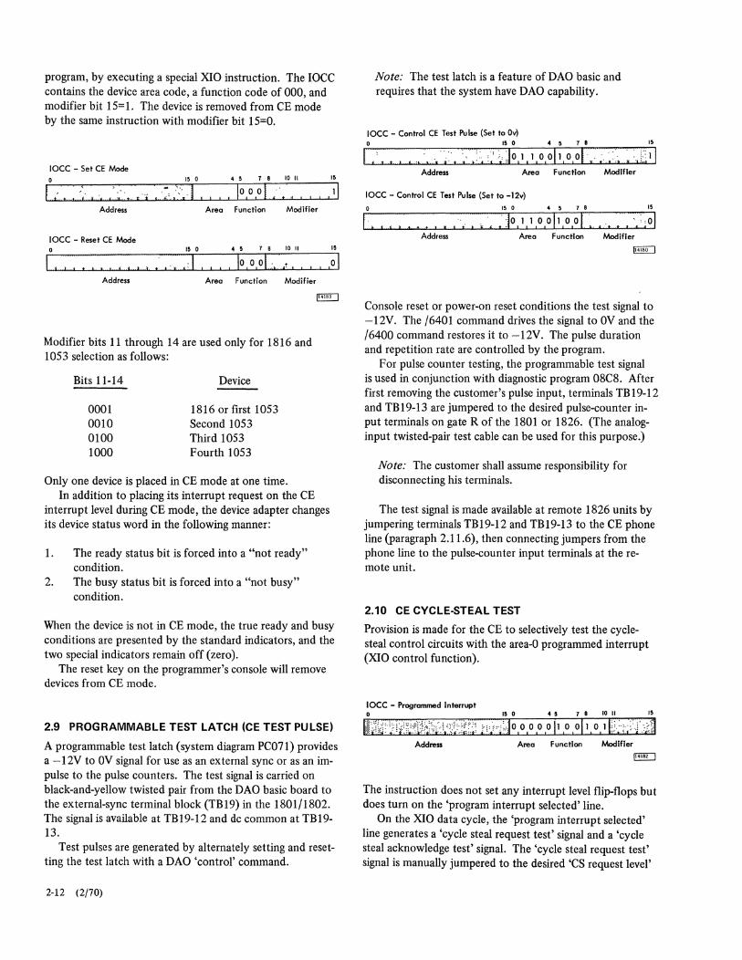
program, by executing a special XIO instruction. The IOCC contains the device area code, a function code of 000, and modifier bit 15= 1. The device is removed from CE mode by the same instruction with modifier bit 15=0.
10CC - Set CE Mode o 15 0 4 5 1 8 10 II 15
I;t::-:':·,,'~'·t:'''' (·;,:<·1 1"10 ,0,01,-.,,, " ,II Address Area Function Modifier
10CC - Reset CE Mode 15 0 4 5 1 B 10 II 15
I , ::::: : . : ( f f
Address Area F unction Modifier
Modifier bits 11 through 14 are used only for 1816 and 1053 selection as follows:
Bits 11-14
0001 0010 0100 1000
Device
1816 or first 1053 Second 1053 Third 1053 Fourth 1053
Only one device is placed in CE mode at one time. In addition to placing its interrupt request on the CE
interrupt level during CE mode, the device adapter changes its device status word in the following manner:
1. The ready status bit is forced into a "not ready" condition.
2. The busy status bit is forced into a "not busy" condition.
When the device is not in CE mode, the true ready and busy conditions are presented by the standard indicators, and the two special indicators remain off (zero).
The reset key on the programmer's console will remove devices from CE mode.
2.9 PROGRAMMABLE TEST LATCH (CE TEST PULSE)
A programmable test latch (system diagram PC071) provides a -12V to OV signal for use as an external sync or as an impulse to the pulse counters. The test signal is carried on black-and-yellow twisted pair from the DAO basic board to the external-sync terminal block (TBI9) in the 1801/1802. The signal is available at TB19-12 and dc common at TBI9-13.
Test pulses are generated by alternately setting and resetting the test latch with a DAO 'control' command.
2-12 (2/70)
Note: The test latch is a feature of DAO basic and requires that the system have DAO capability.
10CC - Control CE Test Pulse (Set ta Ov) o 15 0 4 5 1 8 15
I.',. I f •• :.·.·~:·, ~ •• ·»>JOIIII,o,oll,o,oL·;./: ::'/ill Address Area Functlan Modifier
10CC - Control CE Test Pulse (Set to -12v) 15 0 4 5 7 8 15
! . Address Area Function Modifier
Console reset or power-on reset conditions the test signal to -12V. The /6401 command drives the signal to OV and the /6400 command restores it to -12V. The pulse duration and repetition rate are controlled by the program.
For pulse counter testing, the programmable test signal is used in conjunction with diagnostic program 08C8. After first removing the customer's pulse input, terminals TB19-12 and TB19-13 are jumpered to the desired pulse-counter input terminals on gate R of the 1801 or 1826. (The analoginput twisted-pair test cable can be used for this purpose.)
Note: The customer shall assume responsibility for disconnecting his terminals.
The test signal is made available at remote 1826 units by jumpering terminals TB 19-12 and TB 19-13 to the CE phone line (paragraph 2.11.6), then connecting jumpers from the phone line to the pulse-counter input terminals at the remote unit.
2.10 CE CYCLE-STEAL TEST
Provision is made for the CE to selectively test the cyclesteal control circuits with the area-O programmed interrupt (XIO control function).
10CC - Progrmnmed Interrupt o 15 0 4 5 7 8 10 II 15
Yi\~:·}:ri!~~!U~}:~?<)L;tt~; %i~<~JO,O 1°,0,0 il ,0,01 1, O,J[;;·;-/LiD Address Area Function Modifier
The instruction does not set any interrupt level flip-flops but does turn on the 'program interrupt selected' line.
On the XIO data cycle, the 'program interrupt selected' line generates a 'cycle steal request test' signal and a 'cycle steal acknowledge test' signal. The 'cycle steal request test' signal is manually jumpered to the desired 'CS request level'
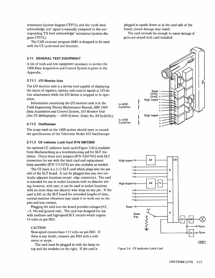
terminator (system diagram CT971), and the 'cycle steal acknowledge test' signal is manually jumpered to the corresponding 'CS level acknowledge' terminator (system diagram CT971).
The CAR exerciser program 08B5 is designed to be used with the CE cycle-steal test function.
2.11 GENERAL TEST EQUIPMENT
A list of tools and test equipment necessary to service the 1800 Data Acquisition and Control System is given in the Appendix.
2.11.1 I/O Monitor Unit
The I/O monitor unit is a service tool capable of displaying the status of registers, latches, and control signals in I/O device attachments while the I/O device is stopped or in operation.
Information concerning the I/O monitor unit is in the Field Engineering Theory-Maintenance Manual, IBM 1800 Data Acquisition and Control System, I/O Monitor Unit (See FE Bibliography -1800 System, Order No. SY26-0550.)
2.11.2 Oscilloscope
The scope used on the 1800 system should meet or exceed the specifications of the Tektronix Model 453 Oscilloscope.
2.11.3 CE I ndicator Latch Card (P/N 5801358)
An optional CE indicator latch card (Figure 2-4) is available from Mechanicsburg as a troubleshooting aid for SLT machines. Thirty-three inch jumpers (PIN 4203785) with SLT connectors for use with the latch card and replacement lamp assembly (P/N 5711078) are also available as needed.
The CE latch is a 2-12 SLT card which plugs into the pin side of the SLT board. It can be plugged into any two vertically adjacent locations except edge connectors. The card is intended for use in socket locations with no discrete wiring; however, with care, it can be used in socket locations with no more than one discrete wire wrap on any pin. If the card is left on the SLT board for extended lengths of time, normal machine vibrations may cause it to work out on the pins and lose contact.
Plugging the card into the board provides voltages (+3, -3, +6) and ground only. The card was designed for use with medium- and high-speed SLT circuits which require +3 volts on pin D03.
CAUTION Slow-speed circuits have +12 volts on pin D03. If there is any doubt, measure pin D03 with a voltmeter or scope.
The card must be plugged in with the lamp on top and the modules on the right. If the card is
plugged in upside down or in the card side of the board, circuit damage may result.
The card extends far enough to cause damage if gates are closed with card installed.
Reset -SYNC -SYNC +
{ High Imped +
In AND + +
Condition + +
{ High Imped -
In AND + +
Condition + +
High Imped-o----\
+o-------~
+ A +o-------~
+o---------~
High Imped+o----I
+0---------1 A +0---------1 +o-------------~
+o------------~
Reset- o------------~
Reset Key
Figure 2-4. CE Indicator Latch Card
A
OR
1800 FEMM (2/10) 2-13
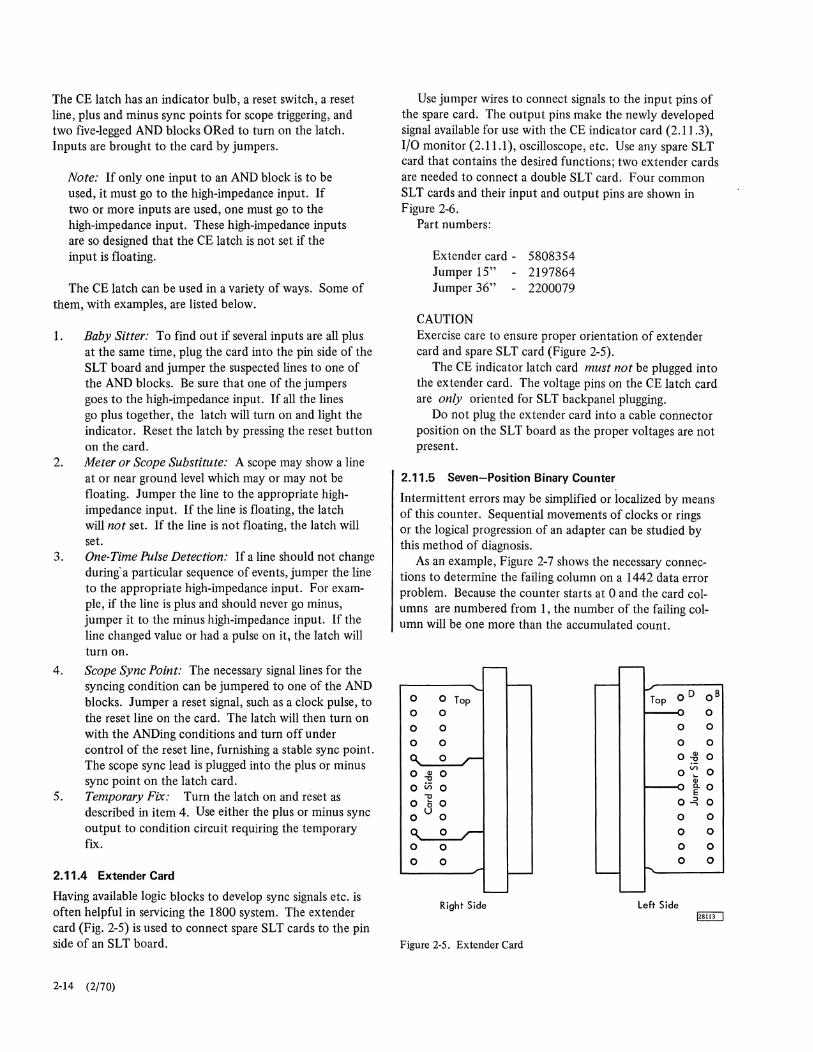
The CE latch has an indicator bulb, a reset switch, a reset line, plus and minus sync points for scope triggering, and two five-legged AND blocks ORed to turn on the latch. Inputs are brought to the card by jumpers.
Note: If only one input to an AND block is to be used, it must go to the high-impedance input. If two or more inputs are used, one must go to the high-impedance input. These high-impedance inputs are so designed that the CE latch is not set if the input is floating.
The CE latch can be used in a variety of ways. Some of them, with examples, are listed below.
1. Baby Sitter: To find out if several inputs are all plus at the same time, plug the card into the pin side of the SLT board and jumper the suspected lines to one of the AND blocks. Be sure that one of the jumpers goes to the high-impedance input. If all the lines go plus together, the latch will turn on and light the indicator. Reset the latch by pressing the reset button on the card.
2. Meter or Scope Substitute: A scope may show a line at or near ground level which mayor may not be floating. Jumper the line to the appropriate highimpedance input. If the line is floating, the latch will not set. If the line is not floating, the latch will set.
3. One-Time Pulse Detection: If a line should not change during'a particular sequence of events, jumper the line to the appropriate high-impedance input. For example, if the line is plus and should never go minus, jumper it to the minus high-impedance input. If the line changed value or had a pulse on it, the latch will turn on.
4. Scope Sync Point: The necessary signal lines for the syncing condition can be jumpered to one of the AND blocks. Jumper a reset signal, such as a clock pulse, to the reset line on the card. The latch will then turn on with the ANDing conditions and turn off under control of the reset line, furnishing a stable sync point. The scope sync lead is plugged into the plus or minus
5. sync point on the latch card. Temporary Fix: Turn the latch on and niset as described in item 4. Use either the plus or minus sync output to condition circuit requiring the temporary fix.
2.11.4 Extender Card
HaVing available logic blocks to develop sync signals etc. is often helpful in servicing the 1800 system. The extender card (Fig. 2-5) is used to connect spare SLT cards to the pin side of an SLT board.
2-14 (2/70)
Use jumper wires to connect signals to the input pins of the spare card. The output pins make the newly developed signal available for use with the CE indicator card (2.11.3), I/O monitor (2.11.1), oscilloscope, etc. Use any spare SLT card that contains the desired functions; two extender cards are needed to connect a double SLT card. Four common SLT cards and their input and output pins are shown in Figure 2-6.
Part numbers:
Extender card - 5808354 Jumper IS" - 2197864 Jumper 36" - 2200079
CAUTION Exercise care to ensure proper orientation of extender card and spare SLT card (Figure 2-5).
The CE indicator latch card must not be plugged into the extender card. The voltage pins on the CE latch card are only oriented for SLT backpanel plugging.
Do not plug the extender card into a cable connector position on the SLT board as the proper voltages are not present.
2.11.5 Seven-Position Binary Counter
Intermittent errors may be simplified or localized by means of this counter. Sequential movements of clocks or rings or the logical progreSSion of an adapter can be studied by this method of diagnosis.
As an example, Figure 2-7 shows the necessary connections to determine the failing column on a 1442 data error problem. Because the counter starts at 0 and the card columns are numbered from 1, the number of the failing column will be one more than the accumulated count.
~
r--0 o Top Top OD oB
0 0 0
0 0 0 0
0 0 0 0
0-8 0
o ~ 0 8.. 0 E
o ~ 0
0 0
0 0
0 0
o 0 0 0
"' -'--
Right Side Left Side ~
Figure 2-5. Extender Card
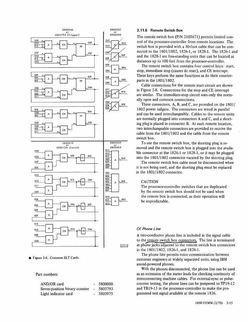
5800040 or
5803794 (Trigger)
009
FF
007
809
FF
006
804
FF
002
5800319 or
5803130 (Lotch)
• Figure 2-6. Common SLT Cards
Part numbers:
AND/OR card Seven-position binary counter Light indicator card
5800207 or 2.11.6 Remote Switch Box
5800000 The remote switch box (P/N 2105671) permits limited con-
~ 010 trol of the processor-controller from remote locations. The 013 switch box is provided with a 30-foot cable that can be con-
~ nected to the 1801/1802, 1826-1, or 1828-1. The 1826-1 and
809 and the 1828-1 are free-standing units that can be located at distances up to 100 feet from the processor-controller.
803 The remote switch box contains four control keys: start,
~ 005 stop, immediate stop (causes dc reset), and CE interrupt.
~ These keys perform the same functions as do their counter-
006 parts in the 1801/1802. D09 A
Cable connections for the remote start circuit are shown in Figure 2-8. Connections for the stop and CE interrupt are similar. The immediate-stop circuit uses only the norm-ally open and common connections.
Three connectors, A, B, and C, are provided on the 1801/ 1802 power tailgate. The connectors are wired in parallel and can be used interchangeably. Cables to the remote uni~s are normally plugged into connectors A and C, and a short-ing plug is placed in connector B. At each remote location, two interchangeable connectors are provided to receive the cable from the 1801/1802 and the cable from the remote switch box.
5800209 To use the remote switch box, the shorting plug is re-or
5800004 moved and the remote switch box is plugged into the availa-011 012 ble connector at the 1826-1 or 1828-1, or it may be plugged 813 into the 1801/1802 connector vacated by the shorting plug. 009 A
810 809 The remote switch box cable must be disconnected when 006 007 it is not being used, and the shorting plug must be replaced 002 in the 1801/1802 connector. 804 805 803 A 802 CAUTION 004
The processor-controller switches that are duplicated 808 807 by the remote switch box should not be used when 010 the remote box is connected, as their operation will
~ be unpredictable. 01
CE Phone Line
A two-conductor phone line is included in the signal cable to the remote switch box connectors. The line is terminated
J28114AJ at phtne jacks adjacent to the remote switch box connectors in the 1801/1802,1826-1, and 1828-1.
- 5800000 - 5803793 - 5803975
The phone line permits voice communication between customer engineers at widely separated units, using IBM sound-powered phones.
With the phones disconnected, the phone line can be used as an extension of the meter leads for checking continuity of interconnecting machine cables. For external-sync or pulsecounter testing, the phone lines can be jumpered to TP 19-12 and TBI9-13 in the processor-controller to make the programmed test signal available at the remote 1826.
1800 FEMM (2/70) 2-15
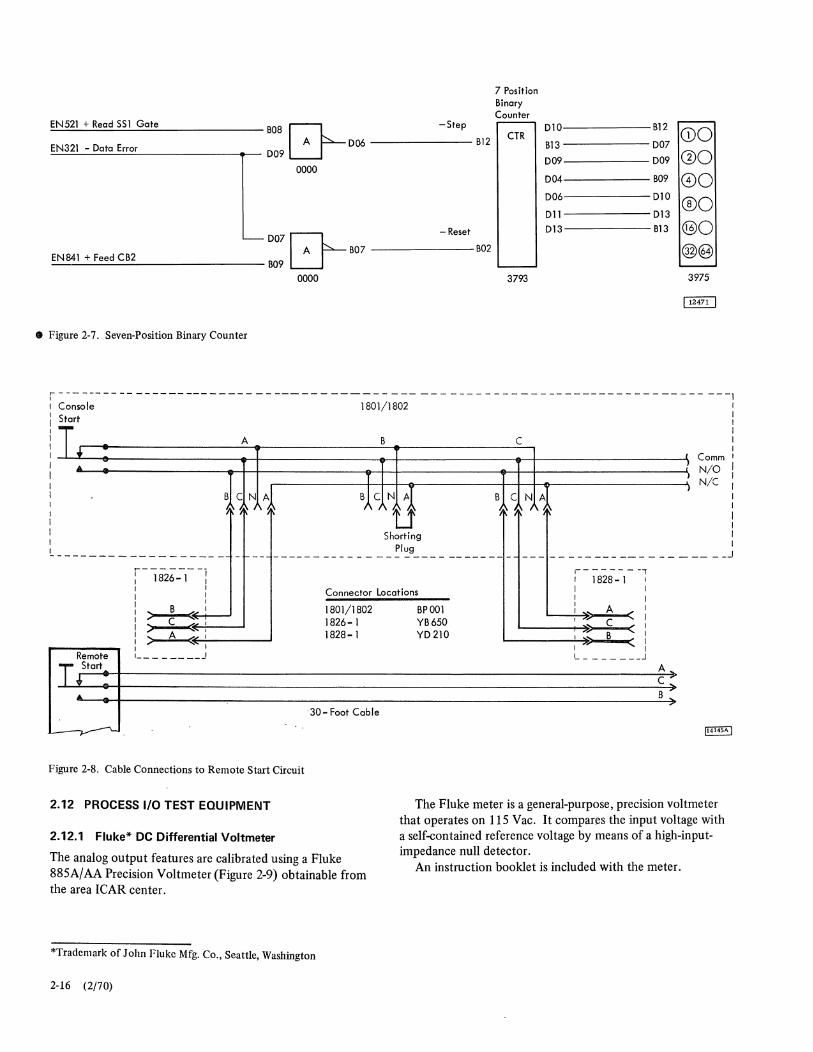
7 Position Binary Counter
EN521 + Read 551 Gate B08&
-Step 010 B12
A 006 B12 CTR (DO EN321 - Oata Error B13 007
009 009 009 Q)O
0000 004 B09 00 006 010 ®O 011 013 013 B13 @O
0078-- Reset
A B07 B02 @@ EN841 + Feed CB2 B09
0000 3793 3975
112471 1
• Figure 2-7. Seven-Position Binary Counter
r- - -- ----- -- -------------- -- ----- - ----- - - -- --- --- - - - -- -- - -- ------- - -- - -- --- ---1
Console 1801/1802 I
~ : T. A B C
... ! Comm
)
B C N A B C N AJ ~ ~~ /\ 1\ U B C
~ N A /\ ~
., N/O N/C
Shorting Plug ----------------- - - -- ---------------------------- --- - - - - - -- - -- - - - - -
'--1826_-1- -j r- -- - - --j
I 1828-1 I I Connector Locations I I I I I
Remote Start
I
) B
~ I
C :> ~ I
A I
;::. ((! I
I ________ J
Figure 2-8. Cable Connections to Remote Start Circuit
2.12 PROCESS I/O TEST EQUIPMENT
2.12.1 Fluke* DC Differential Voltmeter
1801/1802 1826-1 1828-1
'30 - Foot Cable
The analog output features are calibrated using a Fluke 885A/ AA Precision Voltmeter (Figure 2-9) obtainable from the area leAR center.
*Tradcmark of John Flukc Mfg. Co., Seattle, Washington
2-16 (2/70)
I BPOOI I A I
YB650 I ill C < I
ill < I Y0210 I I B
..... I I I L _______ J
A C B
The Fluke meter is a general-purpose, precision voltmeter that operates on 115 Vac. It compares the input voltage with a self-contained reference voltage by means of a high-inputimpedance null detector.
An instruction booklet is included with the meter.

Figure 2-9. Fluke Precision Voltmeter (PIN 453191)
Figure 2-10. Analog Input Calibration Facility
2.12.2 Analog Input Calibration Facility
The analog input calibration facility (Figure 2-10) is housed in the 1828-2 Enclosure that abuts the 1801, 1802, or 1826 containing the AI basic boards. The calibration facility is mounted inside the upper right-hand side of the 1828-2 frame and is accessible from the rear of the enclosure.
Primary power is supplied to the calibration facility through the AI calibration switch on the left side of the 1828 bonnet.
The calibration facility consists of a 30-volt ungrounded power supply, a precision voltage reference unit of 6.3 volts, a resistive divider network, and a high-level solid-state multiplex switch. The circuit schematic is shown on system diagram YD120.
The calibration facility provides the following dc refererice voltages (nominal) for calibration of AI features:
+5 volts -5 volts 500mV 200mV
100mV 50mV 20mV lOmV
1800 FEMM (2/70) 2-17
Exact voltages between terminals are measured at the factory and are recorded (to five significant digits) on the reference unit.
The analog reference voltage can be connected to the special multiplex switch (terminals A and C) for direct switching onto the analog input coaxial cable under program control. The coaxial output of the calibration facility connects to the AI coaxial input cable at the "T" connector (terminal 5) of the last 1851 Multiplexer Terminal installed in the 1828. The special multiplex switch is selected by multiplexer address 113E8, which is outside the normal range of MPX/S addresses. (Actually, any address I 13xx will select the special switch.)
When the analog reference voltage is not being used for calibration, the coaxial cable is left connected for +5V switched input to the analog input bus, and the AI calibration switch is left on. The multiplexed calibration point can be addressed at any time by the customer program or diagnostic program for an operational check on the ADC.
For ADC calibration, and for checking accuracy and repeatability on systems with MPX/S inputs, the output of the multiplexed calibrate point (terminals A and B) is connected directly to the input terminal block on the ADC board. The coaxial cable is disconnected at each end and is replaced by a twisted-pair cable that is provided with the calibration facility.
For calibration of differential (low-level) amplifiers, the analog reference voltage is disconnected from the multiplex switch input and is connected via twisted pair from the appropriate low-level output terminals on the calibrate card to an unused MPX/R input point assigned to the amplifier being calibrated. The reference voltage is connected in this same manner when running accuracy and repeatability checks on systems with MPX/R inputs.
Precautions
The following precautions should be observed to prevent damage to the calibration source or impairment of its accuracy.
1. Do not connect calibration source to customer terminals until current element and customer lines have been removed by customer.
2. Do not connect calibration source to more than one analog input at a time.
3. Do not permit prolonged shorting of calibration source output terminals.
4. Because of impedance mismatch, accurate measurements are not possible if the calibration source is connected directly to a solid-state input point.
2.12.3 Digital Input Test Card
The digital-input test card (PIN 2195669) is used in conjunction with diagnostic programs 0824 and 0825 to test the
2-18 (2/70)
digital-input and process-interrupt features. The test card provides a known digital-input bit configuration to any desired DI or PI group (16 pOints) for reading by the program.
The DI test card consists of a specially wired SLT connector card fitted with two 12-inch leads. Lead 1 is connected to bit positions 0-2-4-6-8-10-12-14 of the test card, and lead 2 is connected to bit positions 1-3-5-7-9-11-13-15.
For testing digital inputs or process interrupts, the input cable from the "R" gate is disconnected at the socket on the adapter board, and the test card is plugged onto the pins of the same socket on the reverse (pin) side of the board.
CAUTION The SL T board can be destroyed if the test card is installed upside down. The card is labeled to indicate proper orientation.
DI PI Group Group Socket
o 1 2 3 4 5 6 7
1 2 3
N2 N3 N4 N5 N6 N7 A6 A7
The test leads are connected to either +3V (D03 pin) or -3V (B06 pin), depending on the bit pattern desired. Pin connections for various bit patterns are shown in the following table.
Pin Connection Resulting Bit Pattern Hex
Lead 1 Lead 2
003 B06 1010101010101010 AAAA
B06 003 0101010101010101 5555
003 003 1111111111111111 FFFF
B06 B06 0000000000000000 0000
2.12.4 Digital Output Test Cable
The digital-output test cable (PIN 2195696) is used in conjunction with diagnostic program 0827 to test the digital output feature.
The DO test cable consists of a lO-foot cable with a serpent connector on one end and an SLT connector card on the other end.
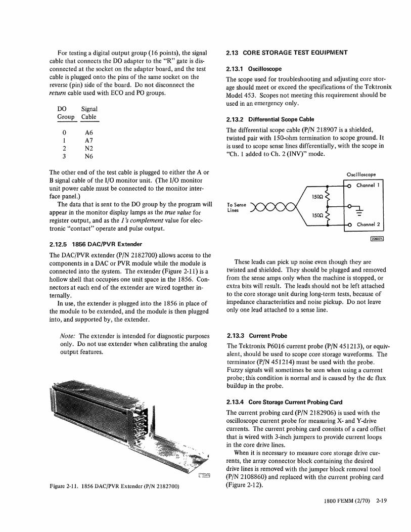
For testing a digital output group (16 points), the signal cable that connects the DO adapter to the "R" gate is disconnected at the socket on the adapter board, and the test cable is plugged onto the pins of the same socket on the reverse (pin) side of the board. Do not disconnect the return cable used with ECO and PO groups.
DO Signal Group Cable
o A6 I A7 2 N2 3 N6
The other end of the test cable is plugged to either the A or B signal cable of the I/O monitor unit. (The I/O monitor unit power cable must be connected to the monitor interface panel.)
The data that is sent to the DO group by the program will appear in the monitor display lamps as the troe value for register output, and as the 1 's complement value for electronic "contact" operate and pulse output.
2.12.5 1856 DAC/PVR Extender
The DAC/PVR extender (P/N 2182700) allows access to the components in a DAC or PVR module while the module is connected into the system. The extender (Figure 2-11) is a hollow shell that occupies one unit space in the 1856. Connectors at each end of the extender are wired together internally.
In use, the extender is plugged into the 1856 in place of the module to be extended, and the module is then plugged into, and supported by, the extender.
Note: The extender is intended for diagnostic purposes only. Do not use extender when calibrating the analog output features.
Figure 2-11. 1856 DAC/PVR Extender (P/N 2182700)
2.13 CORE STORAGE TEST EQUIPMENT
2.13.1 Oscilloscope
The scope used for troubleshooting and adjusting core storage should meet or exceed the speCifications of the Tektronix Model 453. Scopes not meeting this requirement should be used in an emergency only.
2.13.2 Differential Scope Cable
The differential scope cable (P/N 218907 is a shielded, twisted pair with lSO-ohm termination to scope ground. It is used to scope sense lines differentially, with the scope in "Ch. 1 added to Ch. 2 (INV)" mode.
To Sense Lines
Oscilloscope
These leads can pick up noise even though they are twisted and shielded. They should be plugged and removed from the sense amps only when the machine is stopped, or extra bits will result. The leads should not be left attached to the core storage unit during long-term tests, because of impedance characteristics and noise pickup. Do not leave only one lead attached to a sense line.
2.13.3 Current Probe
The Tektronix P6016 current probe (P/N 451213), or equivalent, should be used to scope core storage waveforms. The terminator (P/N 451214) must be used with the probe. Fuzzy signals will sometimes be seen when using a current probe; this condition is normal and is caused by the dc flux buildup in the probe.
2.13.4 Core Storage Current Probing Card
The current probing card (P/N 2182906) is used with the oscilloscope current probe for measuring X- and Y-drive currents. The current probing card consists of a card offset that is wired with 3-inch jumpers to provide current loops in the core drive lines.
When it is necessary to measure core storage drive currents, the array connector block containing the desired drive lines is removed with the jumper block removal tool (P/N 2108860) and replaced with the current probing card (Figure 2-12).
1800 FEMM (2/70) 2-19
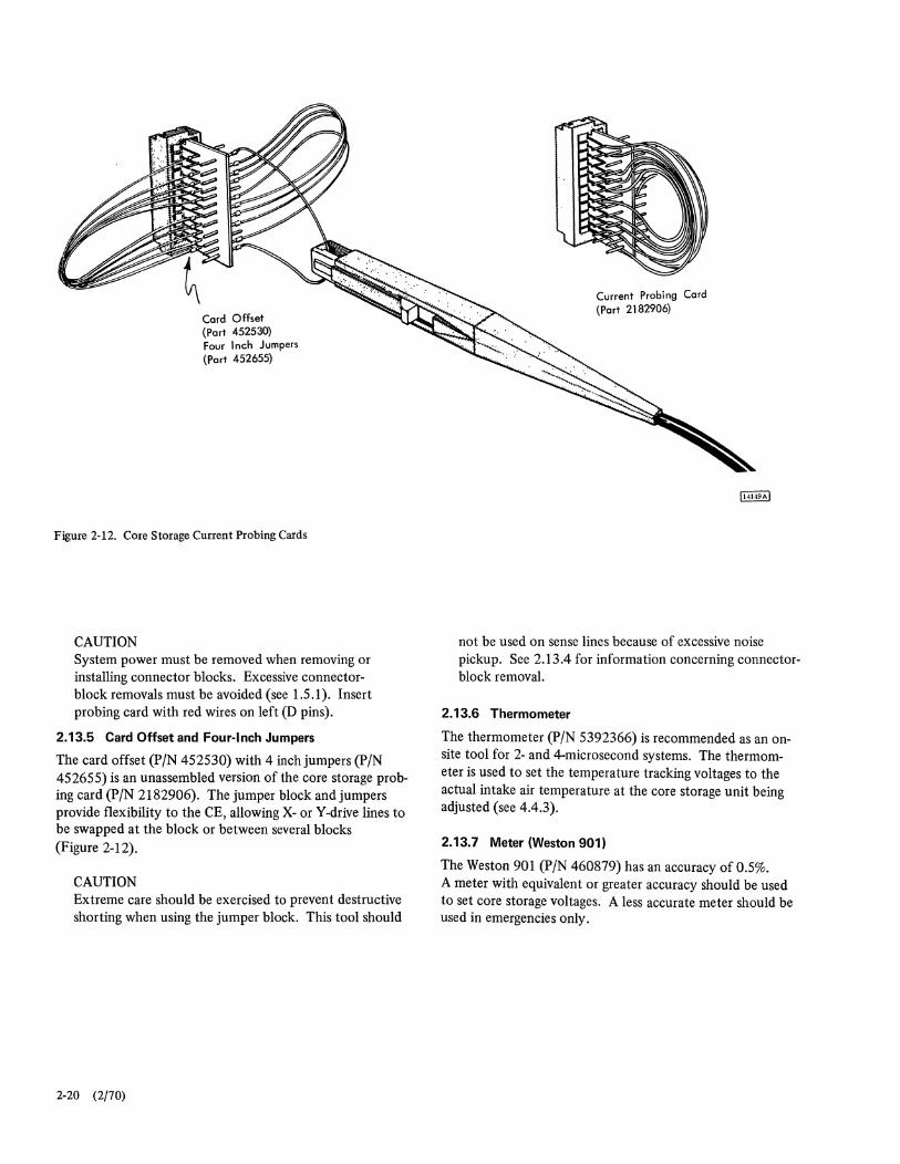
Card Offset (Part 452530) Four Inch Jumpers (Part 452655)
Figure 2-12. Core Storage Current Probing Cards
CAUTION System power must be removed when removing or installing connector blocks. Excessive connectorblock removals must be avoided (see 1.5.1). Insert probing card with red wires on left (D pins).
2.13.5 Card Offset and Four-Inch Jumpers
The card offset (pIN 452530) with 4 inch jumpers (PIN 452655) is an unassembled version of the core storage probing card (PIN 2182906). The jumper block and jumpers provide flexibility to the CE, allowing X- or Y-drive lines to be swapped at the block or between several blocks (Figure 2-12).
CAUTION Extreme care should be exercised to prevent destructive shorting when using the jumper block. This tool should
2-20 (2/70)
Current Probing Card (Part 2182906)
not be used on sense lines because of excessive noise pickup. See 2.13.4 for information concerning connectorblock removal.
2.13.6 Thermometer
The thermometer (PIN 5392366) is recommended as an onsite tool for 2- and 4-microsecond systems. The thermometer is used to set the temperature tracking voltages to the actual intake air temperature at the core storage unit being adjusted (see 4.4.3).
2.13.7 Meter (Weston 901)
The Weston 901 (PIN 460879) has an accuracy of 0.5%. A meter with equivalent or greater accuracy should be used to set core storage voltages. A less accurate meter should be used in emergencies only.
The 1800 system is designed for minimum routine maintenance, as shown in Figure 3-1.
Filter cleaning and replacement is the primary preventive maintenance function. In a relatively clean and air-conditioned environment, filters should not require changing more often than the six-month interval. In particularly dusty environments, it will be necessary to check and replace filters on a schedule learned by experience on the particular system.
Fans and blower motors in the SLT gates and power supplies have sealed bearings that are permanently lubricated.
Code Location or Freq
U R Operation
Chapter 3. Preventive Maintenance
Electromechanical DP I/O units require maintenance according to their published schedules. As with filter replacement, these schedules will have to be adjusted according to the dictates of usage, rate of wear, and environment.
It should not be necessary to run diagnostic programs on a scheduled basis. The exception is where the customer's programming detects the possibility of failures of a specific or nonspecific nature or where the diagnostic program is utilized as a calibration or adjustment check.
Operation Reference
0 Filter, As Check for dirty filters; replace as required. Check cooling fons for proper operation. Sections 4.2.2 Blower Req 5.4.3
8 AOC Check AOC accuracy and repeatability and recalibrate if necessary. Refer to system System logi cs for cal ibrate procedure. Olagrams
3 Amplifier Check and recalibrate, if necessary, fhe buffer or sample and hold amplifier in the Q0810, Q0815
1801/1802/1826 and the differential amplifiers in 1851 'so Refer to system logic for calibrate procedure.
6 1 Analog Check and recal ibrate, if necessary, the Analog Output feature. System Oiag
Output Note: Fluke 885 A/M Precision Voltmeter is required and can be obtained from TA002 Area ICAR Center.
9 Misc Inspect for loose connectors, SLT boards, modules, etc. Check system grounding net-work and line cord for correct operation and safe condition •
• Figure 3-1. 1800 System Preventive Maintenance Chart (Series 4)
1800 FEMM (2/70) 3-1
Chapter 4. Checks, Adjustments, and Removals
Section 1. Basic Unit
4.1 PANEL LAMPS
Indicator lamps and message lamps used in the IBM 1800 Data Acquisition and Control System are removable from the front of the panel.
4.1.1 Indicator Lamp Removal/Replacement
1. Grasp burned-out lamp with thumb and forefinger and pull straight out.
2. Insert new lamp in socket. The lamp and socket are keyed for correct alignment.
4.1.2 Message Lamp Removal/Replacement
1. Remove message button by pulling straight out. 2. Remove old lamp and insert new one, using tool,
PIN 461163. 3. Reinstall message button by pressing straight in.
4.2 GATE BLOWERS
4.2.1 Blower Removal/Replacement
The gate blower assemblies are designed for quick removal. Blower motor lubrication is not required.
1. Remove mainline power. 2. Disconnect the blower power plug at the hinge end of
the gate. 3. Support the blower assembly with one hand. Turn the
latch (Figure 4-1) counterclockwise and uncouple the latch.
4. Support the blower assembly with both hands and pull the assembly away from the hinge end of the gate.
5. Replace the blower assembly by reversing the removal procedure.
6. Turn on mainline power and check blower for proper operation.
4.2.2 Filter Replacement
All blower assemblies in the SLT gates contain replaceable filters. These filters must be inspected regularly on a schedule dictated by the environment and replaced whenever air flow is obviously being restricted. It is not necessary to remove power when replacing gate filters; however, care must be taken not to contact electrical connections with filters that have metal frames.
1. Open SLT gate. 2. Grasp sides of filter at end of gate opposite gate hinges
and pull down to release filter from the plunger retainer.
3. Pull filter from the lip on the hinge end of the gate and lift out.
Note: Plastic filters can be cleaned by vacuuming or by washing in warm water that contains a mild soap or detergent. If filters are cleaned by washing, a system of rotation should be set up whereby a thoroughly dry filter is available to replace the one that is presently removed. Filters that are cleaned by vacuuming should be reinstalled so that the direction of airflow is the same as it was before removal. Discard any filter that shows signs of deterioration.
4. Install clean, dry filter by inserting under lip at hinge end of gate and snapping into position.
4.3 CENTRAL PROCESSING UNIT
4.3.1 Service Check
The diagnostic monitor header program 0800 provides a quick check of basic CPU functions, and indicates those areas that require further checking.
4.3.2 Phase A/B Adjustment
Phase A and phase B pulse durations should be equal within 10%. Favor a shorter phase B pulse duration. Adjustment is made at the I-volt level of positive transition.
Set up scope as follows:
Vert (Chan 1 and 2): 1 V/div Horizontal: 50 ns/div (2 J.J.s); 100 ns/div (4 J.J.s) Sync: -, B phase Mode: Alternate
To adjust: 1. Place mode switch in run position. 2. Scope '+A phase power' at B-B2F2105 (system dia
gram CC021). 3. Scope '+B phase power' at B-B2F211O. 4. Adjust oscillator potentiometer at B-B214 for correct
phase-A and phase-B pulse widths.
18pO FEMM (2/70) 4-1
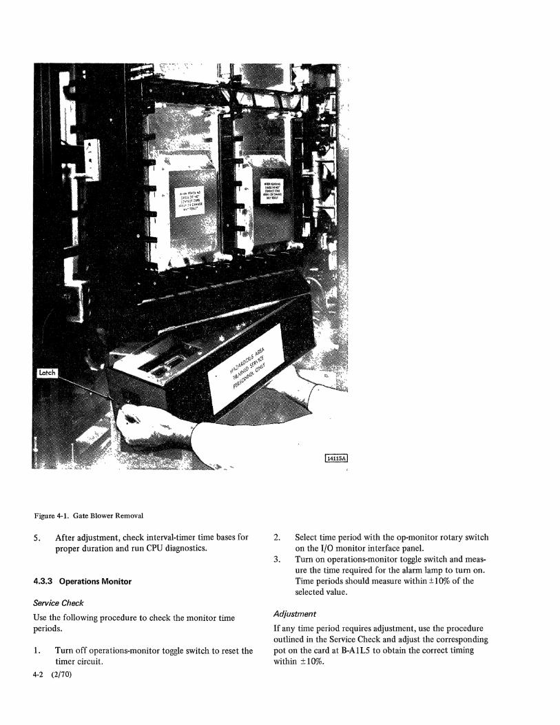
Figure 4-1. Gate Blower Removal
5. After adjustment, check interval-timer time bases for proper duration and run CPU diagnostics.
4.3.3 Operations Monitor
Service Check
Use the following procedure to check the monitor time periods.
1. Turn off operations-monitor toggle switch to reset the timer circuit.
4-2 (2/70)
2.
3.
Select time period with the op-monitor rotary switch on the I/O monitor interface panel. Turn on operations-monitor toggle switch and measure the time required for the alarm lamp to turn on. Time periods should measure within ± 10% of the selected value.
Adjustment
If any time period requires adjustment, use the procedure outlined in the Service Check and adjust the corresponding pot on the card at B-AIL5 to obtain the correct timing within ± 10%.
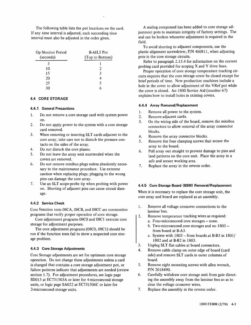
The following table lists the pot locations on the card. If any time interval is adjusted, each succeeding time interval must also be adjusted in the order given.
Op Monitor Period (seconds)
5 10 15 20 25 30
4.4 CORE STORAGE
4.4.1' General Precautions
B-AIL5 Pot (Top to Bottom)
1 2 3 4 5 6
1. Do not remove a core storage card with system power on.
2. Do not apply power to the system with a core storage card removed.
3. When removing or inserting SLT cards adjacent to the core array, take care not to disturb the pressure contacts on the sides of the array.
4. Do not disturb the core planes. 5. Do not leave the array unit unattended when the
covers are removed. 6. Do not remove minibus plugs unless absolutely neces
sary to the maintenance procedure. Use extreme caution when replacing plugs; plugging to the wrong pins can damage the core array.
7. Use an SLT scope-probe tip when probing with power on. Shorting of adjacent pins can cause circuit damage.
4.4.2 Service Check
Core function tests 08CA, 08CB, and 08CC are nonmonitor programs that verify proper operation of core storage.
Core adjustment programs 08CO and 08CI exercise core storage for adjustment purposes.
The core adjustment programs (08CO, 08CI) should be run if the function tests fail to show a suspected core storage problem.
4.4.3 Core Storage Adjustments
Core Storage adjustments are set for optimum core storage operation. Do not change these adjustments unless a card is changed that contains a core storage adjustment pot, or failure patterns indicate that adjustments are needed (review section 1.7). For adjustment procedures, see logic page SDOI3 at EC731503A or later for 4-microsecond storage units, or logic page SA022 at EC731506C or later for 2-microsecond storage units.
A sealing compound has been added to core storage adjustment pots to maintain integrity of factory settings. The seal can be broken whenever adjustment is required in the field.
To avoid shorting to adjacent components, use the plastic alignment screwdriver, P/N 460811, when adjusting pots in the core storage circuits.
Refer to paragraph 2.13.4 for information on the current probing card provided for scoping X and Y drive lines.
Proper operation of core storage temperature tracking circuits requires that the core storage cover be closed except for brief periods of time. New production machines include a hole in the cover to allow adjustment of the VRef pot while the cover is closed. An 1800 Service Aid (number 67) explains how to install holes in existing covers.
4.4.4 Array Removal/Replacement
1. Remove all power to the system. 2. Remove adjacent cards. 3. On the wiring side of the board, remove the minibus
connectors to allow removal of the array connector blocks.
4. Remove the array connector blocks. 5. Remove the four clamping screws that secure the
array to the board. 6. Pull array out straight to prevent damage to pins and
land patterns on the core unit. Place the array in a safe and secure working area.
7. Replace the array in the reverse order.
4.4.5 Core Storage Board (BSM) Removal/Replacement
When it is necessary to replace the core storage unit, the core array and board are replaced as an assembly.
1. Remove all voltage crossover connections to the laminar bus.
2. Remove temperature tracking wires as required: a. Four-microsecond core storages - none. b. Two-microsecond core storages and no 1803 -
from board at B-A3. c. System with 1803 - from boards at B-B3 in 1801/
1802 and at B-B2 in 1803. 3. Unplug SLT flat cables at board connectors. 4. Remove cable clamp on outer edge of board (card
side) and remove SLT cards in outer columns of board.
5. Remove eight mounting screws with allen wrench, P/N 2018490.
6. Carefully withdraw core storage unit from gate directing the assembly away from the laminar bus so as to clear the voltage crossover wires.
7. Replace the assembly in the reverse order.
1800 FEMM (2/70) 4-3
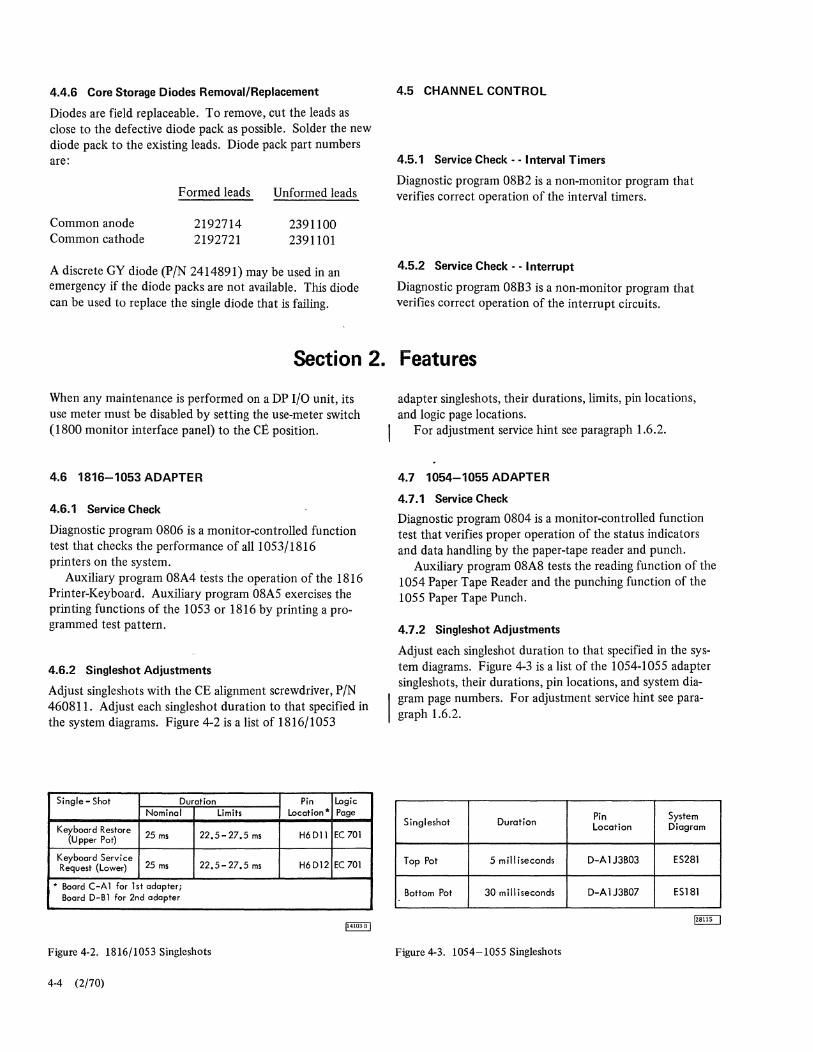
4.4.6 Core Storage Diodes Removal/Replacement
Diodes are field replaceable. To remove, cut the leads as close to the defective diode pack as possible. Solder the new diode pack to the existing leads. Diode pack part numbers are:
Common anode Common cathode
Formed leads
2192714 2192721
Unformed leads
2391100 2391101
A discrete GY diode (P/N 2414891) may be used in an emergency if the diode packs are not available. This diode can be used to replace the single diode that is failing.
Section 2.
When any maintenance is performed on a DP I/O unit, its use meter must be disabled by setting the use-meter switch (1800 monitor interface panel) to the CE position.
4.6 1816-1053 ADAPTER
4.6.1 Service Check
Diagnostic program 0806 is a monitor-controlled function test that checks the performance of all1053/1816 printers on the system.
Auxiliary program 08A4 tests the operation of the 1816 Printer-Keyboard. Auxiliary program 08A5 exercises the printing functions of the 1053 or 1816 by printing a programmed test pattern.
4.6.2 Singleshot Adjustments
Adjust singleshots with the CE alignment screwdriver, PIN 460811. Adjust each singleshot duration to that specified in the system diagrams. Figure 4-2 is a list of 1816/1053
Single - Shot Duration Pin Logic Nominal limits Location * Page
Keyboard Restore (Upper Pot) 25 ms 22.5 - 27.5 ms H6Dll EC 701
Keyboard Service Request (Lower) 25 ms 22.5 - 27.5 ms H6D12 EC 701
* Board C-A 1 far 1st adapter; Board D-B 1 for 2nd adapter
Figure 4-2. 1816/1053 Singieshots
4-4 (2/70)
4.5 CHANNEL CONTROL
4.5.1 Service Check - - I nterval Timers
Diagnostic program 08B2 is a non-monitor program that verifies correct operation of the interval timers.
4.5.2 Service Check - - Interrupt
Diagnostic program 08B3 is a non-monitor program that verifies correct operation of the interrupt circuits.
Features
adapter singleshots, their durations, limits, pin locations, and logic page locations.
For adjustment service hint see paragraph 1.6.2.
4.7 1054-1055 ADAPTER
4.7.1 Service Check
Diagnostic program 0804 is a monitor-controlled function test that verifies proper operation of the status indicators and data handling by the paper-tape reader and punch.
Auxiliary program 08A8 tests the reading function of the 1054 Paper Tape Reader and the punching function of the 1055 Paper Tape Punch.
4.7.2 Singleshot Adjustments
Adjust each singleshot duration to that specified in the system diagrams. Figure 4-3 is a list of the 1054-1055 adapter singleshots, their durations, pin locations, and system diagram page numbers. For adjustment service hint see paragraph 1.6.2.
Singleshot Duration Pin System Location Diagram
Top Pot 5 mill iseconds D-A1J3B03 ES281
Bottom Pot 30 mill iseconds D-A lJ3B07 ES181
Figure 4-3. 1054-1055 Singieshots
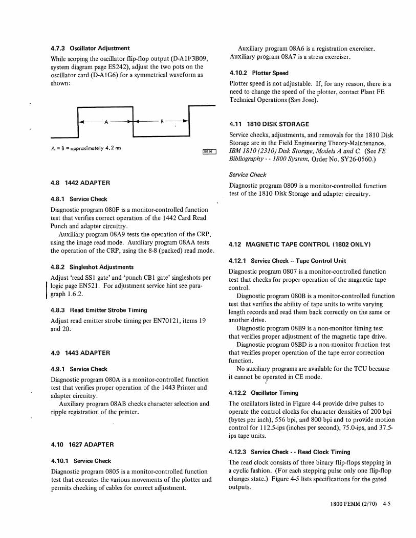
4.7.3 Oscillator Adjustment
While scoping the oscillator flip-flop output (D-AIF3B09, system diagram page ES242), adjust the two pots on the oscillator card (D-AIG6) for a symmetrical waveform as shown:
~I A = B = approximately 4.2 ms
4.8 1442 ADAPTER
4.8.1 Service Check
Diagnostic program 080F is a monitor-controlled function test that verifies correct operation of the 1442 Card Read Punch and adapter circuitry.
Auxiliary program 08A9 tests the operation of the CRP, using the image read mode. Auxiliary program 08AA tests the operation of the CRP, using the 8-8 (packed) read mode.
4.8.2 Singleshot Adjustments
Adjust 'read SSI gate' and 'punch CBl gate' singleshots per
!IOgiC page EN521. For adjustment service hint see paragraph 1.6.2.
4.8.3 Read Emitter Strobe Timing
Adjust read emitter strobe timing per EN70121, items 19 and 20.
4.9 1443 ADAPTER
4.9.1 Service Check
Diagnostic program 080A is a monitor-controlled function test that verifies proper operation of the 1443 Printer and adapter circuitry.
Auxiliary program 08AB checks character selection and ripple registration of the printer.
4.10 1627 ADAPTER
4.10.1 Service Check
Diagnostic program 0805 is a monitor-controlled function test that executes the various movements of the plotter and permits checking of cables for correct adjustment.
Auxiliary program 08A6 is a registration exerciser. Auxiliary program 08A 7 is a stress exerciser.
4.10.2 Plotter Speed
Plotter speed is not adjustable. If, for any reason, there is a need to change the speed of the plotter, contact Plant FE Technical Operations (San Jose).
4.11 1810 DISK STORAGE
Service checks, adjustments, and removals for the 1810 Disk Storage are in the Field Engineering Theory-Maintenance, IBM 1810 (2310) Disk Storage, Models A and C (See FE Bibliography - -1800 System, Order No. SY26-0560.)
Service Check
Diagnostic program 0809 is a monitor-controlled function test of the 1810 Disk Storage and adapter circuitry.
4.12 MAGNETIC TAPE CONTROL (1802 ONLY)
4.12.1 Service Check -- Tape Control Unit
Diagnostic program 0807 is a monitor-controlled function test that checks for proper operation of the magnetic tape control.
Diagnostic program 080B is a monitor-controlled function test that verifies the ability of tape units to write varying length records and read them back correctly on the same or another drive.
Diagnostic program 08B9 is a non-monitor timing test that verifies proper adjustm~nt of the magnetic tape drive.
Diagnostic program 08BD is a non-monitor function test that verifies proper operation of the tape error correction function.
No auxiliary programs are available for the TCU because it cannot be operated in CE mode.
4.12.2 Oscillator Timing
The oscillators listed in Figure 4-4 provide drive pulses to operate the control clocks for character densities of 200 bpi (bytes per inch), 556 bpi, and 800 bpi and to provide motion control for 112.5-ips (inches per second), 75.0-ips, and 37.5-ips tape units.
4.12.3 Service Check - - Read Clock Timing
The read clock consists of three binary flip-flops stepping in a cyclic fashion. (For each stepping pulse only one flip-flop changes state.) Figure 4-5 lists specifications for the gated outputs.
1800 FEMM (2/70) 4-5
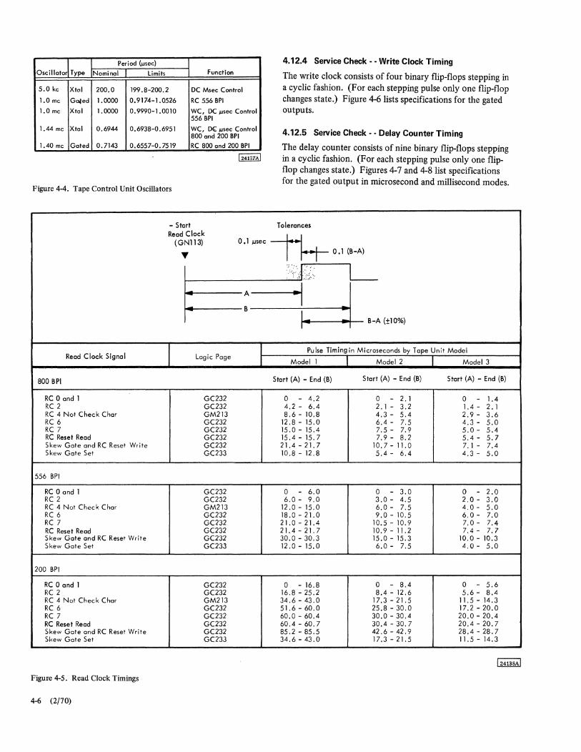
Period (,.Jsec) Osc i lIator Type Nominal I limits I
5.0 kc Xtol 200.0 199.8-200.2
1.0 mc Gated 1.0000 0.9174-1.0526
1.0 mc Xtal 1.0000 0.9990-1. 00 10
1.44 mc Xtal 0.6944 0.6938-0.6951
1.40 mc Gated 0.7143 0.6557-0.7519
Figure 4-4. Tape Control Unit Oscillators
- Start
Function
DC Msec Control
RC 556 BPI
WC, DC psec Control 556 BPI
WC, DG: psec Control 800 and 200 BPI RC 800 and 200 BPI
4.12.4 Service Check - - Write Clock Timing
The write clock consists of four binary flip-flops stepping in a cyclic fashion. (For each stepping pulse only one flip-flop changes state.) Figure 4-6 lists specifications for the gated outputs.
4.12.5 Service Check - - Delay Counter Timing
The delay counter consists of nine binary flip-flops stepping in a cyclic fashion. (For each stepping pulse only one flipflop changes state.) Figures 4-7 and 4-8 list specifications for the gated output in microsecond and millisecond modes.
Tolerances Read Clack
( GN1l3) 0.1 }Jsec --n-r-T 0.1 (B-A)
:~':;Hl"
A l ~ B
B-A (±10%)
Read Clack Signal Logic Page Pulse Timing in Microseconds by Tape Unit Model
Model I Model 2 Model 3
800 BPI Start (A) - End (B) Start (A) - End (8) Start (A) - End (8)
RC 0 and 1 GC232 0 - 4.2 0 - 2.1 0 - 1.4 RC 2 GC232 4.2 - 6.4 2.1 - 3.2 1.4- 2.1 RC 4 Not Check Char GM213 8.6 - 10.8 4.3 - 5.4 2.9- 3.6 RC 6 GC232 12.8 - 15.0 6.4 - 7.5 4.3 - 5.0 RC 7 GC232 15.0 - 15.4 7.5 - 7.9 5.0 - 5.4 RC Reset Read GC232 15.4-15.7 7.9 - 8.2 5.4 - 5.7 Skew Gate and RC Reset Write GC232 21.4-21.7 10.7-11.0 7.1 - 7.4 Skew Gate Set GC233 10.8 - 12.8 5.4 - 6.4 4.3 - 5.0
556 BPI
RC 0 and 1 GC232 0 - 6.0 0 - 3.0 0 - 2.0 RC 2 GC232 6.0 - 9.0 3.0 - 4.5 2.0- 3.0 RC 4 Not Check Char GM213 12.0 - 15.0 6.0 - 7.5 4.0- 5.0 RC 6 GC232 18.0-21.0 9.0 - 10.5 6.0- 7.0 RC 7 GC232 21.0-21.4 10.5 - 10.9 7.0- 7.4 RC Reset Read GC232 21.4-21.7 10.9 - 11.2 7.4 - 7.7 Skew Gate and RC Reset Write GC232 30.0-30.3 15.0 - 15.3 10.0 - 10.3 Skew Gate Set GC233 12.0-15.0 6.0 - 7.5 4.0- 5.0
200 BPI
RC 0 and 1 GC232 0 - 16.8 0 - 8.4 0 - 5.6 RC 2 GC232 16.8 - 25.2 8.4 - 12.6 5.6 - 8.4 RC 4 Not Check Char GM213 34.6 - 43.0 17.3 - 21.5 11.5 - 14.3 RC 6 GC232 51.6 - 60.0 25.8-30.0 17.2 - 20.0 RC 7 GC232 60.0 - 60.4 30.0 - 30.4 20.0-20.4 RC Reset Read GC232 60.4 - 60.7 30.4 - 30.7 20.4-20.7 Skew Gate and RC Reset Write GC232 85.2 - 85.5 42.6 - 42.9 28.4-28.7 Skew Gate Set GC233 34.6 - 43.0 17.3 - 21.5 11.5 - 14.3
Figure 4-5. Read Clock Timings
4-6 (2/70)
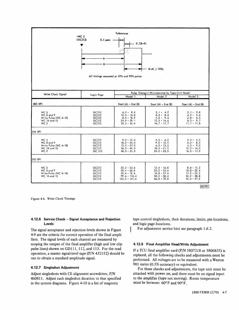
Tolerances -WC 2
!40.1(8-A)
(GC312) 0.1 "sec
...
I: <T :t~±1~) A
8 r All timings measured at 10% and 90% points
Write Clock Signal Logic Page Pulse Timing in Microseconds by Tape Unit Model
I Modell I Model 2 I Model 3
800 8PI Start (A) - End (8) Start (A) - End (8) Start (A) - End (8)
we 5 Ge312 6.3 - 8.4 3.1 - 4.2 2.1 - 2.8 we 8 and 9 Ge312 12.6 - 16.8 6.3 - 8.4 4.2 - 5.6 Write Pulse (We 6-10) Ge312 8.4 - 18.9 4.2 - 9.4 2.8 - 6.3 WC 14 and 15 Ge312 24.9 - 29.1 12.5-14.6 8.3 - 9.7 we 2 Ge312 33.3 - 35.4 16.7-17.7 11.1-11.8
556 8PI
we 5 Ge312 9.0 - 12.0 4.5 - 6.0 3.0 - 4.0 we 8 and 9 Ge312 18.0 - 24.0 9.0 - 12.0 6.0 - 8.0 Write Pulse (We 6-10) Ge312 12.0 - 27.0 6.0 - 13.5 4.0 - 9.0 we 14 and 15 Ge312 36.0 - 42.0 18.0 - 21.0 12.0 - 14.0 we 2 Ge 312 48.0-51.0 24.0 - 25.5 16.0 - 17.0
200 8PI
we 5 Ge312 25.2 - 33.6 12.4 - 16.8 8.4-11.2 we 8 and 9 Ge312 50.4 - 66.8 25.2 - 33.6 16.8 - 22.4 Write Pulse (We 6-10) Ge312 33.6 - 75.6 16.8 - 37.6 11.2 - 25.2 we 14 and 15 Ge312 99.6 - 116.4 50.0 - 58.4 33.2 - 38.8
Ge312 133.2 - 141.6 66.8 - 70.8 44.4 - 47.2
Figure 4-6. Write Clock Timings
4.12.6 Service Check -- Signal Acceptance and Rejection tape control singleshots, their durations, limits, pin locations, and logic page locations. Levels
The signal acceptance and rejection levels shown in Figure 4-9 are the criteria for correct operation of the final amplifiers. The signal levels of each channel are measured by scoping the output of the final amplifier (high and low clip pulse lines) shown on GDlll, 112, and 113. For the read operation, a master Signal-level tape (PIN 432152) should be run to obtain a standard amplitude signal.
4.12.7 Singleshot Adjustment
Adjust singieshots with CE alignment screwdriver, PIN 460811. Adjust each single shot duration to that specified in the system diagrams. Figure 4-10 is a list of magnetic
I For adjustment service hint see paragraph 1.6.2.
4.12.8 Final Amplifier Read/Write Adjustment
If a TCD final amplifier card (pIN 5807218 or 5806835) is replaced, all the following checks and adjustments must be performed. All voltages are to be measured with a Weston 901 meter (0.5% accuracy) or equivalent.
For these checks and adjustments, the tape unit must be attached with power on, and there must be no signal input to the amplifier (tape not moving). Room temperature must be between 60° F and 90° F.
1800 FEMM (2/70) 4-7.
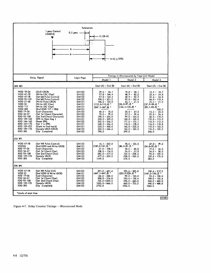
Tolerances
+ }!Sec Control 0.1 j.lSeC ----ti-t-- 0.1 (B-A)
(GM214)
'Y
~ ;1 ~~±I~ A
B
Delay Signal Logic Page Timings in Microseconds by Tape Unit Model
Modell Model 2 Model 3
SOO BPI Start (A) - End (B) Start (A) - End (B) Start (A) - End (B)
WOO 19-26 (Shift CRCR) GN123 39.6 - 56.1 19.5 - 2S.1 13.2 - IS.7 WOO 47-78 (Write CRC Char) GN123 97.S - 164.4 48.9- 82.2 32.6 - 54.8 WOO 47-78 (Set WR Pulse Control) GM132 97.S - 164.4 48.9- 82.2 32.6 - 54.8 WOO 95-159 (Set WR Pulse Control) GM132 198.0-331.2 99.0 - 165.6 66.0 - 110.4 WOO 51-58 (Write Pulse CRCR) GM131 106.2 - 123.0 53.1 - 61.5 35.4 - 41.0 WOO 53 (Write LRC Char) GM131 (112.3-113.0) * (56.5-57.2) * (37.9-38.6) • WOO 117 (Write LRC Char) GM131 (247.1-247.8) * (124.1-124.8) * (83.1-83.8) * WOO 403 (End WOO 117 + 286) GM131 ------ ------ 280.0 ROD 19-36 (Lost Character) GN122 40.0 - 75.0 20.0 - 37.5 13.3 - 25.0 ROD 36-37 (Set 1st Check Character) GN123 75.0 - 79.2 37.5 - 39.6 25.0 - 26.4 ROD 95-158 (Set 2nd Check Character) GN123 198.0 - 330.0 99.0 - 165.0 66.0 - 110.0 ROD 159-162 (EPR to Skew Reg ) GN121 330.0 - 339.0 165.0-169.5 110.0 - 113.0 ROD 164-165 (Reset EPR) GN122 342.0 - 346.2 171.0 - 173.1 114.0 - 115.4 ROO 167-170 (Set 1 in EPR) GN121 348.0 - 356.4 174.0- 178.2 116.0 - 118.8 ROO 159-222 (Gate to find track) GN121 330.0 - 465.0 165.0 - 232.5 110.0 - 155.0 ROD 159-175 (Sample LRCR-<:RCR) GM133 330.0 - 366.6 165.0 - 183.3 110.0 - 122.2 ROO 383 (Op Complete) GM133 798.0 399.0 266.0
556 BPI
WOO 47-78 (Set WR Pulse Control) GN123 14.1 - 247.0 70.5 - 123.5 47.0 - 79.0 WOO53 (End WOO and Write LRCR) GM131 (160.0-161.0) • (80 .5-81 .5) • (54 .0-55.0) * ROD 19-36 (Lost Character) GN122 57.0-108.0 28.5 - 54.0 19.0 - 36.0 ROD 36-37 (Set 1st Check Char) GNI23 108.0 - 114.0 54.0 - 57.0 36.0 - 38.0 ROD 95-158 (Set 2nd Check Char) GNI23 285.0 - 477.0 142.5 - 238.5 95.0 - 159.0 ROD 159-175 (Sample LRCR) GM133 477.0 - 525.0 238.5 - 262.5 159.0 - 175.0 ROD 383 (Op Complete) GMI33 1149.0 574.4 383.0
200 BPI
WOO 47-78 (Set WR Pulse Ctrl) GNI23 391.2 - 651.6 195.6 - 325.8 130.4 - 217.2 WOO 53 (End WOO & Write LRCR) GM131 (447.1-447.8) * (223.9-224.6) * (149.5-150.2) * ROD 19-36 (Lost Character) GN122 160.0 - 300.0 80.0 - 150.0 53.2 - 100.0 ROD 36-37 (Set 1st Check Char) GN123 300.0 - 316.8 150.0 - 158.4 100.0 - 105.6 ROD 95-158 (Set 2nd Check Char) GN123 742.0-1320.0 396.0 - 660.0 264.0 - 440.0 ROD 159-175 (Sample LRCR) GM133 1320.0-1466.0 660.0 - 733.2 440.0 - 488.8 ROD 383 (Op Complete) GM133 3192.0 1596.0 1064.0
"limits of start time
Figure 4-7. Delay Counter Timings - - Microsecond Mode
4-8 (2/10)

Ref Signal ... ... /4 Timing
ao'
Timings in Milliseconds Delay Signal Logic Page Function Reference 9-Track 7-Track
Madel 3 Tape Unit Min. Max. Min. Max.
End WOO GM 131 Reset Go on Write + MS Control GM214 See Note 1 1.7- 2.0
031 or 53 MS not LP GM132 End WO not LP Rise of Go GM215 5.2 - 5.8 5.2 - 5.8
DI60TA GM133 Set Go in Sackspace + MS Control GM214 15.9 - 17.6 15.9 - 17.6
096 TA GM133 Set Skwd RD or WR + MS Control GM214 9.5 - 10.3 9.5 - 10.3
End Read Delay GM132 End RO not LP Rise of Go GM215 1.4 - 1.6 2.7- 3.1
End R 0 Sac kspace Rise of Go GM215 1. 1 - 1.3 1. 1 - 1.3
End RD LP Rise of Go GM215 15.9 - 17.6 15.9 - 17.6
Sksp Reset Rd Cond. GM131 Reset Rd. Cond & Go on Sksp +ROD GM213 0.6 - .8 1.9- 2.2
WD 320 GM133 End WD OP Rise of Go GM215 31.9- 35.2 31.9- 35.2
WD 32 GM132 Set Read Cond On Rise of Go Write 3.1- 3.5 3.1- 3.5
Mode 2 Tape Unit
End WOO GM131 Reset Go on Write See Note 2 Check Char Check Char 031 or 53 MS not LP GM132 End WD not LP Rise of Go
GM215 6.1 - 6.8 6.1- 6.8 D160TA GM133 Set Go in Sksp +MS Control
GM214 31.9- 35.2 31.9- 35.2 096 TA GM133 Set Skwd RD or Wr + MS Control
GM214 19.1- 21.1 19.1 - 21.1 End Read Delay GM132 End RD not LP Rise of Go
GM215 3.4 - 3.7 6.1- 6.8 End RO Sksp Rise of Go
GM215 1.5- 1.6 1.5- 1.6 End RD LP Rise of Go
GM215 20.5 - 22.7 20.5 - 22.7 Bksp Reset Rd Cond GM131 Reset Rd. Cond & Go on Bksp +ROD
GM213 2.1- 2.4 4.1 - 4.6 WD 320 GM133 End WD LP Rise of Go
GM215 63.9 - 70.4 63.9 - 70.4 WD 17 GM214 Set Read Cond on Write Rise of Go
GM215 3.3 - 3.7 3.3 - 3.7
Modell Tape Unit
End WOO GM131 Reset Go on Write See Note 2 Check Char Check Char 031 or 53 MS not LP GM132 End WD not LP Rise of Go
GM215 12.3 - 13.6 12.3 - 13.6 0160 TA GM133 Set Go in Sksp + MS Control
GM214 63.9 - 70.4 63.9 - 70.4 096 TA GM133 Set Bkwd RD or WR + MS Control
GM214 38.3 - 42.2 38.3 - 42.2 End Read Delay GM132 End RO not LP Rise of Go
GM215 6.7 - 7.5 12.3 - 13.6 End RD Sksp Rise of Go
GM215 1.9- 2.2 1. 9 - 2.2 End RD LP Rise of Go
GM215 41. 1 - 45.3 41. 1 - 45.3 Sksp Reset Rd Cond GM131 Reset Rd Cond & Go on Bksp +ROD
GM213 5.5 - 6.2 9.5 - 10.6 WD 320 GM133 End WD LP Rise of Go
GM215 127.9 - 140.8 127.9- 140.8 WD 17 GM214 Set Read Cond on Write Rise of Go
GM215 6.7- 7.5 6.7- 7.5
Notes 1: End WOO for 9-track model 3 occurs with WOO 403. 2: WOO ends with the reset of write release,Go falls with the set of first check characters with Model lor Model 2.
Figure 4·8. Delay Counter Timings - - Millisecond Mode
1800 FEMM (2/70) 4-9
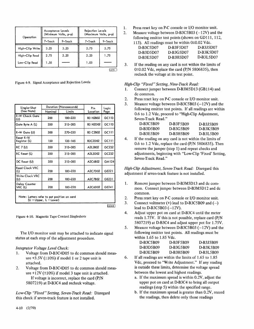
Acceptance Levels Rejectian Levels
Operatian (Minimum Valts, p-p) (Maximum Valts, p-p)
7-Track 9-Track 7-Track 9-Track
High-Clip Write 3.25 3.25 2.75 2.75
Hlgh-C lip Read 2.75 2.25 2.25 1.75
Law-Clip Read 1.55 -- 1.05 --
Figure 4-9. Signal Acceptance and Rejection Levels
Single-Shat Duratian (Nanasecands) Pin Lagic (See Nate) Naminal Limits Lacation Page
R-W Check Gate 200 180-220 B3 H2B02 (U) GC1l3
Gate 8yte A (L) 350 315-385 83 H2D02 GC1l3
R-W Gate (U) 300 270-330 83 C2802 GClll
Reset R-W Register (L) 150 135-165 83C2D02 GClll
RC 7 (U) 350 315-385 A2L3802 GC232
RC Reset (L) 350 315-385 A2L3D02 GC232
DC Reset (U) 350 315-385 A2C6802 GM124
Read Clock VRC (L) 200 180-220 A2C7D02 GE221
Write Clock VRC (U) 200 180-220 A2C7B02 GE231
Delay Counter VRC (L) 200 180-220 A2C6D02 GE241
Note: Letters refer to pot position on card (U = Upper, L = Lower)
Figure 4-10. Magnetic Tape Control Singleshots
The I/O monitor unit may be attached to indicate signal status at each step of the adjustment procedure.
Integrator Voltage Level Check: 1. Voltage from D-B3C4D05 to dc common should meas
ure +3.5V (±1O%) if model 1 or 2 tape unit is attached.
2. Voltage from D-B3C4D05 to dc common should measure +12V (±1O%) if model 3 tape unit is attached.
If voltage is incorrect, replace the card (P /N 5807219) at D-B3C4 and recheck voltage.
Low-Clip "Fixed" Setting, Seven-Track Read: Disregard this check if seven-track feature is not installed.
4-10 (2/70)
1. Press reset key on P-C console or I/O monitor unit. 2. Measure voltage between D-B3C5B03 (-12V) and the
following emitter test points (shown on GD111, 112, 113). All readings must be within 0±0.02 Vdc.
3.
D-B3C5D07 D-B3F5D07 D-B3J5D07 D-B3D5D07 D-B3G5D07 D-B3K5D07 D-B3E5D07 D-B3H5D07 D-B3L5D07
If the reading on any card is not within the limits of 0±0.02 Vdc, replace the card (P/N 5806835), then recheck the voltage at its test point.
High-Clip "Fixed" Setting, Nine- Track Read: 1. Connect jumper between D-B3M5D 13 (GB 114) and
2. 3.
dc common. Press reset key on P-C console or I/O monitor unit. Measure voltage between D-B3C5B03 ( -12V) and the following emitter test points. If all readings are within 0.6 to 1.2 Vdc, proceed to "High-Clip Adjustment, Seven-Track Read."
D-B3C5B09 D-B3F5B09 D-B3D5B09 D-B3G5B09 D-B3E5B09 D-B3H5B09
D-B3J5B09 D-B3K5B09 D-B3L5B09
4. If the reading on any card is not within the limits of 0.6 to 1.2 Vdc, replace the card (P/N 5806835). Then remove the jumper (step 1) and repeat checks and adjustments, beginning with "Low-Clip 'Fixed' Setting, Seven-Track Read."
High-Clip Adjustment, Seven-Track Read: Disregard this adjustment if seven-track feature is not installed.
1. Remove jumper between D-B3M5D13 and dc common. Connect jumper between D-B3M5D12 and dc common.
2. Press reset key on P-C console or I/O monitor unit. 3. Connect voltmeter (+) lead to D-B3C5B09 and (-)
lead to D-B3C5B03 (-12V). 4. Adjust upper pot on card at D-B3C4 until the meter
reads 1.75V. If this is not possible, replace card (P/N 5807219) at D-B3C4 and adjust upper pot for 1.75V.
5. Measure voltage between D-B3C5B03 ( -12V) and the following emitter test points. All readings must be within 1.65 to 1.85 V dc.
D-B3C5B09 D-B3F5B09 D-B3J5B09 D-B3D5B09 D-B3G5B09 D-B3K5B09 D-B3E5B09 D-B3H5B09 D-B3L5B09
6. If all readings are within the limits of 1.65 to 1.85 Vdc, proceed to "Write Adjustment." If any reading is outside these limits, determine the voltage spread between the lowest and highest readings. a. If the maximum spread is within 0.2V, adjust the
upper pot on card at D-B3C4 to bring all output readings (step 5) within the specified range.
b. If the maximum spread is greater than 0.2V, record the readings, then delete only those readings
necessary to bring the spread of the remaining readings within 0.2V. Replace the cards (P/N S80683S) in the channels whose readings were deleted. Then remove the jumper (step 1) and repeat the entire adjustment procedure, beginning with "Low-Clip 'Fixed' Setting, Seven-Track Read."
Write Adjustment: 1. Remove jumper between D-B3MSD 12 and dc com
mon. Connect jumper between D-B2ESB 13 (GB341) and dc common.
2. Press reset key on P-C console or I/O monitor unit. 3. Connect voltmeter (+) lead to D-B3CSB09 and (-)
lead to D-B3CSB03 ( -12V). 4. Adjust lower pot on card at D-B3C4 (level-setter) un
til the meter reads 2.5V. If this is not possible, replace card (part S807219) at D-B3C4 and adjust for 2.SV, then repeat adjustments, beginning with "HighClip Adjustment, Seven-Track Read."
S. Measure voltage between D-B3CSB03 ( -12V) and the following emitter output pins. All readings must be within 2.4 to 2.6 V dc.
D-B3CSB09 D-B3FSB09 D-B3DSB09 D-B3GSB09 D-B3ESB09 D-B3HSB09
D-B3JSB09 D-B3KSB09 D-B3LSB09
6. If all readings are within the limits of 2.4 to 2.6 V dc, proceed to step 7. If any reading is outside these limits, determine the voltage spread between the lowest and highest readings. a. If the maximum spread is within 0.2V, adjust the
lower pot on the card at D-B3C4 to bring all output readings (step S) within the specified range.
b. If the maximum spread is greater than 0.2V, record the readings, then delete only those readings necessary to bring the spread of the remaining readings within 0.2V. Replace the cards (PIN S80683S) in the channels whose readings were deleted. Then remove the jumper (step 1) and repeat the entire adjustment procedure, beginning with "Low-Clip 'Fixed' Setting, Seven-Track Read."
7. Remove jumper between D-B2ESBI3 and dc common. 8. Run diagnostic program 0807. If test does not per
form correctly, check signal acceptance and rejection levels (paragraph 4.12.6).
4.13 SYSTEM/360 ADAPTER
4.13.1 Service Check
Diagnostic programs test the operation of I/O commands, status indicators, data buffer, drivers, and gating controls.
Description
1. PID 08CD enables the CE to test the 1800 side of the adapter while it is off-line to the System/360 channel.
SY26-5956-6 FES: SS27-0724
The System/360 reset line has to be tied down on the 1826 boards to run this test.
2. PID F4D4 may be used to test the System/360 side of the adapter when the 1800 channel has been reterminated or has bypassed the System/360 adapter feature by means of special jumper boards (P/N 2242726). Routines A and B of this section test the transfer of data between the two systems provided that tiedown jumpers are installed as called for on the System/360 printouts when execution of these routines is called for by setting section switch 2 or by instructing the diagnostic monitor to cycle routines A, B, or A and B.
3. PID's 08CE for the 1800 and E4DS for the System/ 360 running concurrently, will test all the functions of the adapter. The System/360 CPU must have available 16k bytes of storage for this test and requires the use ofDMA 4, DMA 8-9, DME, or DM44. PID 08CE does not use the 1800 monitor, but uses the relocatable loader.
4.13.2 Singleshot Adjustments
Adjust the 'transfer' singleshot and the 'tag sample' singleshot per the follOWing procedure. Use the CE alignment screwdriver, PIN 460811.
1. Refer to FY141 and connect a jumper from 26AB3F2D 11 to 26A-B3L3D 1 O. With P-C clock running, scope pin 26A-B3L3B13 and adjust bottom pot on card at 26A-B3L3 so that 'tag sample' pulse (negative) is 300 (±30) nanoseconds wide.
2. Refer to FY201 and connect a jumper from 26AB3F2Dll to 26A-B3L3B07. Scope pin 26A-B3L3D13 and adjust middle pot on card at 26A-B3L3 so that 'transfer SS' pulse (negative) is 300 (±30) nanoseconds wide.
3. Refer to FV2S0 and connect a jumper from 26AB3F2Dli to 26A-B3L3D02. Scope pin 26A-B3L3D12 and adjust the top pot on card at 26A-B3L3 so that the output pulse (negative) is 300 (±30) nanoseconds wide.
4. Remove jumpers attached in steps 1,2, and 3.
S. While running PID 08CD, do the following: a. Scope pin 26A-A3H7B07 and adjust bottom pot
on card at 26A-A3H7 for a 3D-millisecond negative pulse.
b. Scope pin A26-A3H7B03 and adjust top pot on card at 26A-A3H7 for a 3D-millisecond negative pulse. (Refer to ALD FW902 for preceding adjustments.)
4.14 ANALOG INPUT
4.14.1 Precautions
1. Do not remove or install a card in the 18S1 Multiplexer Terminal with system power on.
1800 FEMM (8/70) 4-11
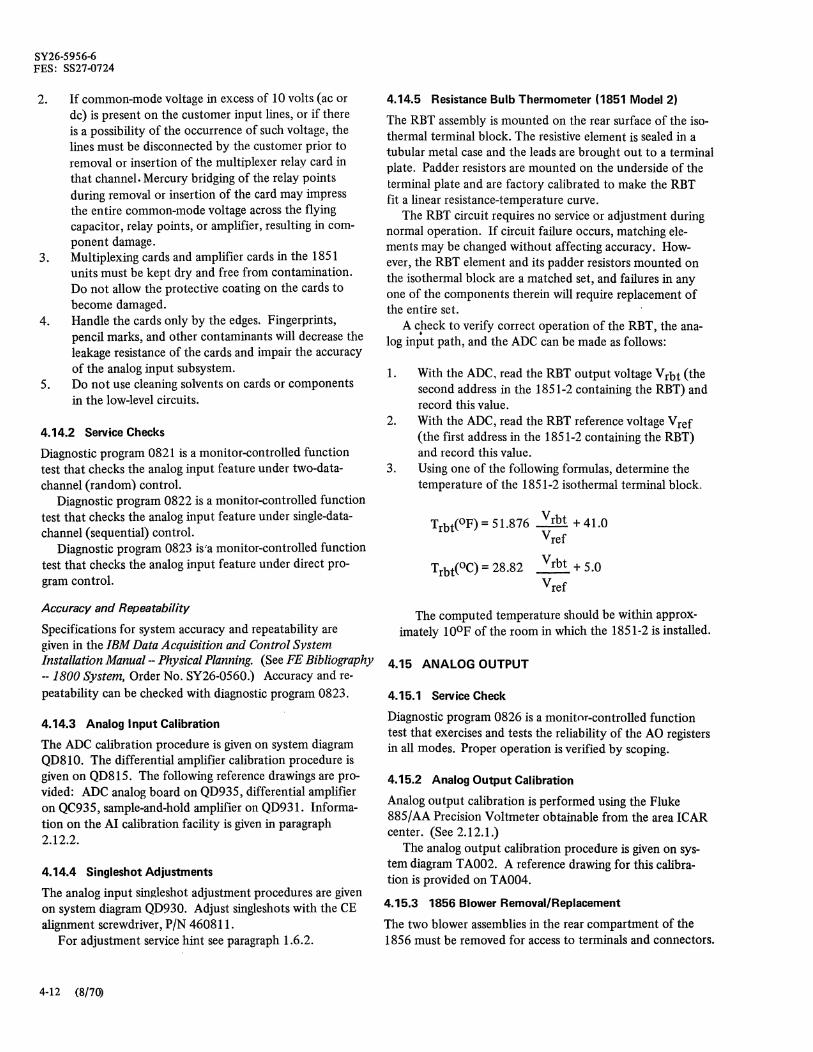
8Y26-5956-6 FE8: 8827-0724
2. If common-mode voltage in excess of 10 volts (ac or dc) is present on the customer input lines, or if there is a possibility of the occurrence of such voltage, the lines must be disconnected by the customer prior to removal or insertion of the multiplexer relay card in that channel. Mercury bridging of the relay points during removal or insertion of the card may impress the entire common-mode voltage across the flying capacitor, relay points, or amplifier, resulting in component damage.
3. Multiplexing cards and amplifier cards in the 1851 units must be kept dry and free from contamination. Do not allow the protective coating on the cards to become damaged.
4. Handle the cards only by the edges. Fingerprints, pencil marks, and other contaminants will decrease the leakage resistance of the cards and impair the accuracy of the analog input subsystem.
5. Do not use cleaning solvents on cards or components in the low-level circuits.
4.14.2 Service Checks
Diagnostic program 0821 is a monitor-controlled function test that checks the analog input feature under two-datachannel (random) control.
Diagnostic program 0822 is a monitor-controlled function test that checks the analog input feature under single-datachannel (sequential) control.
Diagnostic program 0823 is;a monitor-controlled function test that checks the analog input feature under direct program control.
Accuracy and Repeatability
SpeCifications for system accuracy and repeatability are given in the IBM Data Acquisition and Control System Installation Manual- Physical Planning. (See FE Bibliography - 1800 System, Order No. SY26-0560.) Accuracy and repeatability can be checked with diagnostic program 0823.
4.14.3 Analog Input Calibration
The ADC calibration procedure is given on system diagram QD81O. The differential amplifier calibration procedure is given on QD815. The following reference drawings are provided: ADC analog board on QD935, differential amplifier on QC935, sample-and-hold amplifier on QD931. Information on the AI calibration facility is given in paragraph 2.12.2.
4.14.4 Singleshot Adjustments
The analog input singleshot adjustment procedures are given on system diagram QD930. Adjust singleshots with the CE alignment screwdriver, PIN 460811.
For adjustment service hint see paragraph 1.6.2.
4-12 (8/70)
4.14.5 Resistance Bulb Thermometer (1851 Model 2)
The RBT assembly is mounted on the rear surface of the isothermal terminal block. The resistive element is sealed in a tubular metal case and the leads are brought out to a terminal plate. Padder resistors are mounted on the underside of the terminal plate and are factory calibrated to make the RBT fit a linear resistance-temperature curve.
The RBT circuit requires no service or adjustment during normal operation. If circuit failure occurs, matching elements may be changed without affecting accuracy. However, the RBT element and its padder resistors mounted on the isothermal block are a matched set, and failures in any one of the components therein will require replacement of the entire set.
A check to verify correct operation of the RBT, the analog input path, and the ADC can be made as follows:
1. With the ADC, read the RBT output voltage Vrbt (the second address in the 1851-2 containing the RBT) and record this value.
2. With the ADC, read the RBT reference voltage Vref (the first address in the 1851-2 containing the RBT) and record this value.
3. Using one of the follOWing formulas, determine the temperature of the 1851-2 isothermal terminal block.
Trbt(OF) = 51.876 Vrbt + 41.0 Vref
Trbt(oC) = 28.82 Vrbt + 5.0
Vref
The computed temperature should be within approximately 100 F of the room in which the 1851-2 is installed.
4.15 ANALOG OUTPUT
4.15.1 Service Check
Diagnostic program 0826 is a monitor-controlled function test that exercises and tests the reliability of the AO registers in all modes. Proper operation is verified by scoping.
4.15.2 Analog Output Calibration
Analog output calibration is performed using the Fluke 885/AA Precision Voltmeter obtainable from the area ICAR center. (See 2.12.1.)
The analog output calibration procedure is given on system diagram TA002. A reference drawing for this calibration is provided on TA004.
4.15.3 1856 Blower Removal/Replacement
The two blower assemblies in the rear compartment of the 1856 must be removed for access to terminals and connectors.
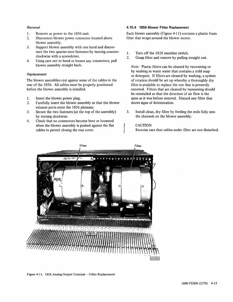
Removal
1. Remove ac power to the 1856 unit. 2. Disconnect blower power connector located above
blower assembly. 3. Support blower assembly with one hand and discon
nect the two quarter-turn fasteners by turning counterclockwise with a screwdriver.
4. Using care not to bend or loosen any connectors, pull blower assembly straight back.
Replacement
The blower assemblies rest against some of the cables in the rear of the 1856. All cables must be properly positioned before the blower assembly is installed.
1. Insert the blower power plug. 2. Carefully insert the blower assembly so that the blower
exhaust ports enter the 1856 plenums. 3. Secure the two fasteners (at the top of the assembly)
by turning clockwise. 4. Check that no connectors become bent or loosened
when the blower assembly is pushed against the flat cables to permit closing the rear cover.
Filter
Figure 4-11. 1856 Analog Output Terminal- - Filter Replacement
4.15.4 1856 Blower Filter Replacement
Each blower assembly (Figure 4-11) contains a plastic foam fIlter that wraps around the blower motor.
1. Turn off the 1828 mainline switch. 2. Grasp filter and remove by pulling straight out.
Note: Plastic fIlters can be cleaned by vacuuming or by washing in warm water that contains a mild soap or detergent. If fIlters are cleaned by washing, a system of rotation should be set up whereby a thoroughly dry fIlter is available to replace the one that is presently removed. Filters that are cleaned by vacuuming should be reinstalled so that the direction of air flow is the same as it was before removal. Discard any filter that shows signs of deterioration.
3. Install clean, dry filter by feeding the ends fully into the channels on the blower assembly.
CAUTION Exercise care that cables under filter are not disturbed.
Filter
1800 FEMM (2/70) 4-13
4.16 DIGITAL INPUT
4.16.1 Service Check - - Digital Input and Process Interrupt
Diagnostic program 0824 is a monitor-controlled function test that checks the operation of digital input features under data-channel control.
Diagnostic program 0825 is a monitor-controlled function test tha,t checks operation of digital input features under direct program control.
The digital-input test card (paragraph 2.12.3) is used with each of these tests to provide a known input bit configuration.
4.16.2 Service Check· - Pulse Counter
Diagnostic program 08C8 (I/O scope routine) is used in conjunction with the programmable CE test pulse (2.9) to check pulse counter operation.
4.17 DIGITAL OUTPUT
4.17.1 Service Check
Diagnostic program 0827 is a monitor-controlled function test that exercises the digital output registers in all modes.
The digital--output test cable (2.12.4) is used with the function test to permit displaying the DO group (16 bits) on the I/O monitor unit.
4.17.2 Singleshot Adjustments
Adjust single shots with CE alignment screwdriver, PIN 460811. Adjust each single shot duration to that specified in the system diagram. Figure 4-12 is a list of digital output singleshots, their durations, limits, pin locations, and logic page locations.
For adjustment service hint see paragraph 1.6.2.
4.18 SELECTOR CHANNEL
4.18.1 Service Check
The follOWing monitor-controlled function tests are provided for checking the operation of the selector channel:
4-14 (2/70)
Single - Shot Duration Pin Nominal Limits Location
PO Busy (Lower Pot) 1.5 ms 1.35-1.65ms B3 E3 004
PO Busy Reset (Lower Pot) 1.5 ms 1.35-1.65 ms B3E4D04
PO Reset 1.5..,sec 1.35-1.65 ..,sec B3E2B02 (Upper Pot)
Figure 4-12. Digital Output Singieshots
0810 0811 0812 0813 0814 0892
Selector channel function test 2841 fUnction test 2311 function test Two-channel switch function test CE pack initialization 2841/2311 MPX on-line test
4.18.2 Singleshot Adjustments
Logic Page
PB051
PB051
PB051
The selector channel single shot adjustments are given on system diagram FSO 11. Adjust single shots with the CE alignment screwdriver, part number 460811.
4.19 COMMUN ICATIONS ADAPTER
4.19.1 Service Check
The following monitor-controlled function tests are provided for checking the operation of the communications adapter:
080E Communications adapter Wraparound 080D Communications adapter transmit/receive 0891 Communications adapter MPX on-line test
4.19.2 Adjustments
No adjustments are required for the communications adapter feature.
Power on/off sequencing for the 1800 system is described in the FE Theory of Operation, Processor-Controller, and is
Chapter 5. Power Su ppl ies
shown graphically in the maintenance diagram manual (FEMDM).
Section 1. Basic Unit
The 1800 system operates from one three-phase mainline power cord. The primary voltage input is 208/230 Yac (+10%;-8%) at 60 Hz, or 195/220/235/380/408 Yac (+10%; -8%) at 50 Hz.
Primary power enters the 1801 or 1802 through a line fIlter and a 50-amp mainline power circuit breaker (CBl) and is sequenced to all system units except the 1053 Printer and the 1816 Printer-Keyboard. The 1053 and 1816 have their own mainline power cords.
For all normal maintenance operations, the circuit breakers on the 1801 or 1802 power sequence box are left on and the system is powered up and down from the on and off switches on the programmer's console. The circuit breakers are provided for isolation of branch circuit overloads, but they may also be tripped manually as a safeguard against power being restored to a unit that has been shut down for servicing.
5.1 PRECAUTIONS
1. Before connecting or disconnecting ac power cables in any system unit, remove primary power as directed in paragraph 1.3.2.
2. Before working on any power supply, remove power from the unit and allow at least one minute for capacitors to discharge. Check the dc output voltage with a meter before attempting maintenance.
3. Remove power before replacing power supply regulator cards.
4. Each power supply heat sink is at an electrical potential when power is on. Do not permit heat sinks to become shorted to one another or to the machine frame.
5. Do not defeat the functions of power sequence relays or sense relays by picking them manually or by jumpering the points, as damage to solid-state components may result.
6. Do not operate power supplies without at least 25% rated load. (See 5.5.1.)
5.2 SYSTEM POWER-ON PROCEDURE
1. Check that operations-monitor switch is off. 2. If System/360 adapter is installed, check that System/
360 is in a stopped condition. 3. Press the on button. Power-on lamp should light and
gate blowers should operate in all units. After a delay of several seconds, the ready lamp should turn on to indicate that dc voltages are present and the system is ready for operation.
4. The lamp.test button may be pressed to check opera· tion of all console indicator (small) lamps.
5.3 SYSTEM POWER·OFF PROCEDURE
1. If System/360 adapter is installed, see 1.3.4. 2. Turn off operations-monitor switch. 3. Press the off button. The off button drops all power
in the system with the exception of the 115-Yac con· venience outlets and the 24-Yac sequencing voltage. In the 1828 Enclosure, the 115 Yac is used to power the AI calibration facility, and the 24 Yac is used to power the PYR-2 zener reference supply.
5.4 ADJUSTMENT AND REMOVAL PROCEDURES.
With the exception of the 48-Y dc supplies and several special-purpose supplies, the 1800 system uses standard MPS (medium power standard) power supplies. They are housed in vertically mounted tubs at the rear of each unit. Servicing access is by opening the rear cover of the bay and by opening the swinging gates at the front.
5.4.1 MPS Power Supply Adjustment
It will be necessary to adjust a power supply output voltage if the regulator card is replaced or if the setting of the voltage adjustment has been changed for marginal checking purposes (1.4) or as a result ofvibration.
1800 FEMM (2/70) 5-1

Before adjusting or replacing a power supply whose output voltage is incorrect, determine that the input voltage at the primary of the power supply transformer is within + 10%, -8% of the nominal value.
An adjustment pot (Rl) on each MPS power supply permits adjusting the output voltage at least ±8%. The lock nut on the adjustment shaft should be tight enough to prevent the shaft from turning due to vibration, but not so tight that the shaft cannot be turned with a screwdriver. Tightening the lock nut after adjustment may cause the shaft to turn and change the voltage setting.
Voltages should be adjusted as close as possible to the nominal value and should be measured with a Weston 901 meter (0.5% accuracy), or equivalent, at the points specified on the follOWing logic pages:
1801/1802 1803 1826-1 or 2 1826-3
YAOlO YS240 YB140 YB240
Voltage measurements are considered valid only after power has been on for at least 15 minutes to allow temperatures to stabilize.
The output of each MPS power supply is adjusted at installation and will change only slightly with aging of regulator components. A change in output voltage in conjunction with a machine failure is often a result of the failure rather than the cause. Do not attempt to correct the trouble by adjusting the power supply voltage.
Figure 5-1. Power Supply Fan Assembly and Air Filter
5-2 (2/70)
5.4.2 MPS Power Supply Removal/Replacement
1. Remove mainline power and take necessary measures to prevent its being restored. Wait at least one minute for capacitors to discharge.
2. Disconnect external leads to the power supply terminal board.
3. Remove the two retaining clips (one at the top, one at bottom) on the exposed ends of the power supply rails. Slide the supply out of the machine.
4. Reverse this procedure to install the supply.
CAUTION If power supply is being replaced, make certain that correct input transformer is provided (50 or 60 Hz) and that transformer primary is wired correctly for the input voltage.
5.4.3 Power Supply Filter Replacement
Fans are mounted at the bottom of each power supply tub. The fan housing contains a replaceable plastic filter (Figure 5-1) that must be periodically inspected, and replaced as required.
Plastic filters can be cleaned by vacuuming or by washing in warm water that contains a mild soap or detergent. If filters are cleaned by washing, a system of rotation should be set up whereby a thoroughly dry filter is available to replace the one that is presently removed. Filters that are cleaned by vacuuming should be reinstalled so that the direction of
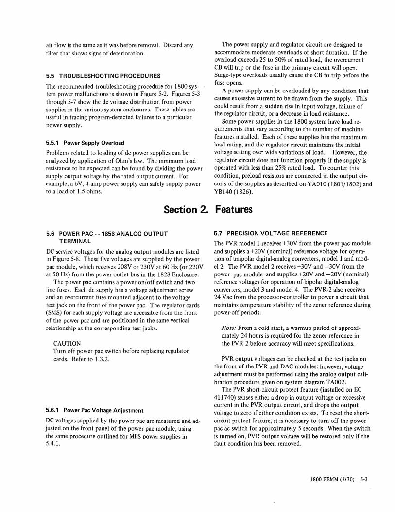
air flow is the same as it was before removal. Discard any filter that shows signs of deterioration.
5.5 TROUBLESHOOTING PROCEDURES
The recommended troubleshooting procedure for 1800 system power malfunctions is shown in Figure 5-2. Figures 5-3 through 5-7 show the dc voltage distribution from power supplies in the various system enclosures. These tables are useful in tracing program-detected failures to a particular power supply.
5.5.1 Power Supply Overload
Problems related to loading of dc power supplies can be analyzed by application of Ohm's law. The minimum load resistance to be expected can be found by dividing the power supply output voltage by the rated output current. For example, a 6V, 4 amp power supply can safely supply power to a load of 1.5 ohms.
Section 2.
5.6 POWER PAC· ·1856 ANALOG OUTPUT TERMINAL
DC service voltages for the analog output modules are listed in Figure 5-8. These five voltages are supplied by the power pac module, which receives 208Vor 230V at 60 Hz (or 220V at 50 Hz) from the power outlet bus in the 1828 Enclosure.
The power pac contains a power on/off switch and two line fuses. Each dc supply has a voltage adjustment screw and an overcurrent fuse mounted adjacent to the voltage test jack on the front of the power pac. The regulator cards (SMS) for each supply voltage are accessible from the front of the power pac and are positioned in the same vertical relationship as the corresponding test jacks.
CAUTION Turn off power pac switch before replacing regulator cards. Refer to 1.3.2.
5.6.1 Power Pac Voltage Adjustment
DC voltages supplied by the power pac are measured and adjusted on the front panel of the power pac module, using the same procedure outlined for MPS power supplies in 5.4.1.
The power supply and regulator circuit are designed to accommodate moderate overloads of short duration. If the overload exceeds 25 to 50% of rated load, the overcurrent CB will trip or the fuse in the primary circuit will open. Surge-type overloads usually cause the CB to trip before the fuse opens.
A power supply can be overloaded by any condition that causes excessive current to be drawn from the supply. This could result from a sudden rise in input voltage, failure of the regulator circuit, or a decrease in load resistance.
Some power supplies in the 1800 system have load requirements that vary according to the number of machine features installed. Each of these supplies has the maximum load rating, and the regulator circuit maintains the initial voltage setting over wide variations of load. However, the regulator circuit does not function properly if the supply is operated with less than 25% rated load. To counter this condition, preload resistors are connected in the output circuits of the supplies as described on Y AO 10 (1801/1802) and YBI40 (1826).
Features
5.7 PRECISION VOLTAGE REFERENCE
The PVR model 1 receives +30V from the power pac module and supplies a +20V (nominal) reference voltage for operation of unipolar digital-analog converters, model 1 and mode12. The PVR model 2 receives +30V and -30V from the power pac module and supplies +20V and -20V (nominal) reference voltages for operation of bipolar digital-analog converters, model 3 and model 4. The PVR-2 also receives 24 Vac from the processor-controller to power a circuit that maintains temperature stability of the zener reference during power-off periods.
Note: From a cold start, a warmup period of approximately 24 hours is required for the zener reference in the PVR-2 before accuracy will meet specifications.
PVR output voltages can be checked at the test jacks on the front of the PVR and DAC modules; however, voltage adjustment must be performed using the analog output calibration procedure given on system diagram T A002.
The PVR short-circuit protect feature (installed on EC 411740) senses either a drop in output voltage or excessive current in the PVR output circuit, and drops the output voltage to zero if either condition exists. To reset the shortcircuit protect feature, it is necessary to turn off the power pac ac switch for approximately 5 seconds. When the switch is turned on, PVR output voltage will be restored only if the fault condition has been removed.
18'00 FEMM (2/70) 5-3

• VI 'rj
,j:. ~. ... '" N VI -- ~ -.l
.9 "<:I 0 ~
'" ... Vl $:: '0 '0
-< >-l ... 0 $:: cr" (D ;. 0 0
S-OC> 0 $:: p: '"
1801/1802
Check fuses, relays, and de volts (Group B of Fig 5 - 3)
Correct trouble, power up, and check de voltages. Run diagnostics if necessary.
Check overcurrent CBs at MPS supplies in 1801/1802 (Graup B of Fig 5-3) and 1826 (Fig 5 and 6)
1803 1826
On
Preliminary checks:
1. Customer description of trouble. 2. Mainline and EPO switches, power-on lights, blowers,
and motors at all units. 3. Open machine covers and check for smoke, acrid odor, etc . 4. Check historical efror log.
No
Check ac power input from 1801/1802 CB2, fuses, relays, and de yolts
Check ac power input from 1801/1802 CB2, fuses, relays, and
Check ac power input 10 1828 from 1801/ 1802 CB3, power pac fuses, and de outputs (Fig 5-8)
Check ac power input: 1053-1816 line cord, 1054-1055 (115 Vae)
from P- C tailgate
1. Check for primary voJtage surge.
2. Check for primary short.
de volts (Fig 5-4) (Fig 5 and 6)
Yes No
1. Replace regulator card. 2. Replace power supply.
switches, 1627 (115 Vae) from P-C.
1442, 1443, 1810 (primary service) from p- C.
2401-2402 (primary service) from 1802 CB4.
Check fuses, circuit breakers, and power su lout ut at unit.
3. Isolate fault by disconnecting portions of load circuit. 4. Check power supply preload- (parograph 5.5.1). 5. Check power supply and input/output circuits for shorts or opens. 6. Check cable connections (power and ground), minibus and
vol tage crossover connections. 7. Scope ac and de lines for intermittent disturbances and noise
(sharp transients may not be detected on the oscilloscope). 8. 1856 power pac-see paragraph 5.6. 9. PVR-see paragraph 5.7.
3. Reset CBl
1. Check primary ekt fuses (Fig 5 - 3).
2. Meter de output of supply as "On" button is pressed.
On
On
Verify mainline input OK: 1. Room dist. panel. 2. Line cord. 3. EPO switeh(es)
Check Fl and F2 (24 Vae)
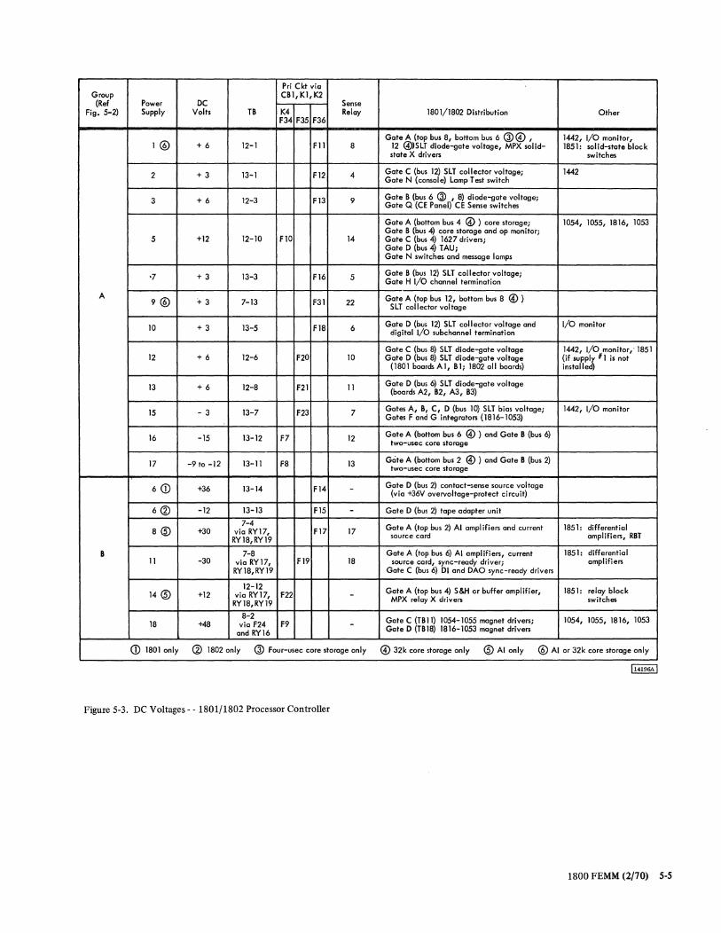
Pri Ckt via Group C81,Kl,K2 (Ref Power DC Sense
Fig. 5-2) Supply Volts T8 K4 Relay 1801/1802 Distribution Other F34 F35 F36
1@ Gate A (top bus 8, bottom bus 6 @@ , 1442, I/O monitor,
+ 6 12-1 Fll 8 12 @)SLT diode-gate voltage, MPX solid- 1851: solid-state block state X drivers switches
2 +3 13-1 F12 4 Gate C (bus 12) SLT collector voltage; Gate N (console) Lamp Test switch
1442
3 + 6 12-3 F13 9 Gate 8 (bus 6 @ , 8) diode-gate voltage; Gate Q (CE Panel) CE Sense switches
Gate A (bottom bus 4 @») core storage; 1054, lOSS, 1816, 1053 Gate 8 (bus 4) core storage and op monitor;
5 +12 12-10 FlO 14 Gate C (bus 4) 1627 drivers; Gate D (bus 4) TAU; Gate N switches and message lamps
q +3 13-3 F16 5 Gate 8 (bus 12) SLT collector voltage; Gate H 1/0 channel termination
A 9@ +3 Gate A (top bus 12, bottom bus 8 @) 7-13 F31 22 SLT collector voltage
10 +3 13-5 F18 6 Gate D (bus 12) SLT collector voltage and digital I/o subchannel termination
I/O monitor
Gate C (bus 8) SLT diode-gate voltage 1442, I/O monitor,· 1851 12 + 6 12-6 F20 10 Gate D (bus 8) SLT diode-gate voltage (if supply # 1 is not
(1801 boards A I, 81; 1802 all boards) installed}
13 + 6 12-8 F21 11 Gate D (bus 6) SLT diode-gate voltage (boards A2, 82, A3, 83)
15 - 3 13-7 F23 7 Gates A, 8, C, D (bus 10) SLT bias voltage; 1442, 1/0 monitor Gates Fond G integrators (1816-1053)
16 -15 13-12 F7 12 Gate A (bottom bus 6 @) ) and Gate 8 (bus 6) two-usee core storage
17 -9 to -12 13-11 F8 13 Gate A (bottom bus 2 @ ) and Gate 8 (bus 2) two-usee core storage
6CD +36 13-14 F14 - Gate D (bus 2) contact-sense source voltage (via +36V overvoltage-protect circuit)
6® -12 13-13 F15 - Gate D (bus 2) tape adapter unit
7-4 Gate A (top bus 2) AI amplifiers and current 1851: di ff erent i a I 8® +30 via RY17, F17 17
RY18,RY19 source card amplifiers, R8T
B 7-8 Gate A (top bus 6) AI ampl ifi ers, current 1851: differential 11 -30 via RY17, F19 18 source card, sync-ready driver; amplifiers
RY18,RY19 Gate C (bus 6) DI and DAO sync-ready drivers
12-12 Gate A (top bus 4) S&H or buffer amplifier, 1851: relay block 14® +12 via RY17, F22 -
RY18,RY19 MPX relay X drivers switches
8-2 Gate C (T81l) 1054-1055 magnet drivers; 1054, lOSS, 1816, 1053 18 +48 via F24 F9 -and RY16 Gate D (T818) 1816-1053 magnet drivers
CD 1801 only (i) 1802 only @ Four-usee core storoge only @ 32k core storage only ® AI only @ Alar 32k core storage only·
Figure 5-3. DC Voltages - - 1801/1802 Processor Controller
1800 FEMM (2/70) 5-5
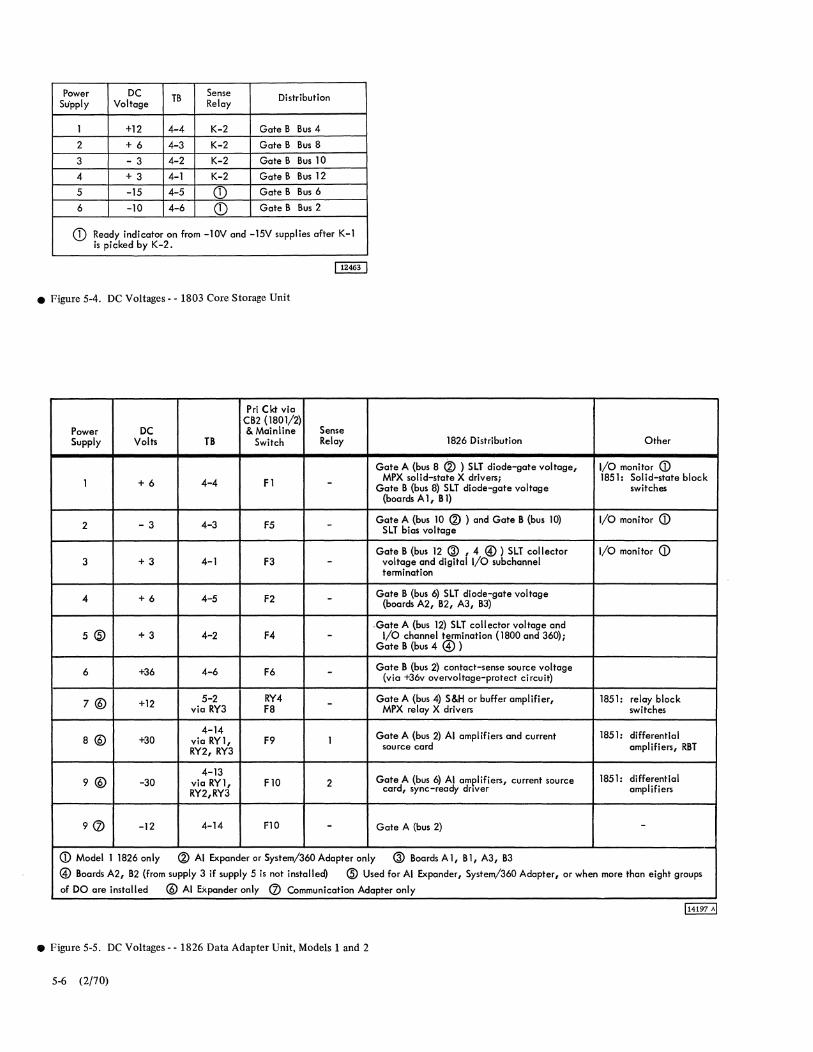
Power DC TB Sense Distribution Supply Voltage Relay
1 +12 4-4 K-2 Gate B Bus 4
2 + 6 4-3 K-2 Gate B Bus 8
3 - 3 4-2 K-2 Gate B Bus 10
4 + 3 4-1 K-2 Gate B Bus 12
5 -15 4-5 CD Gate B Bus 6
6 -10 4-6 CD Gate B Bus 2
CD Ready indicator on from -10V and -15V supplies after K-l is picked by K-2 .
• Figure 5-4. DC Voltages - - 1803 Core Storage Unit
Pri Ckt via CB2 (1801/2)
Power DC & Mainline Sense Supply Volts TB Switch Relay 1826 Distribution Other
Gate A (bus 8 ® ) SLT diode-gate voltage, I/O monitor <D 1 +6 4-4 Fl - MPX solid-state X drivers; 1851: Solid-state block
Gate B (bus 8) SLT dlode-gate voltage switches (boards A I, B 1)
2 - 3 4-3 F5 - Gate A (bus 10 ® ) and Gate B (bus 10) SLT bias voltage
I/O monitor <D
Gate B (bus 12 @ , 4 @) SLT collector I/O monitor <D 3 +3 4-1 F3 - voltage and digital I/O subchannel
termination
4 +6 4-5 F2 - Gate B (bus 6) SLT diode-gate voltage (boards A2, B2, A3, B3)
5® .Gate A (bus 12) SLT collector voltage and
+3 4-2 F4 - I/O channel termination (1800 and 360); Gate B (bus 4 @ )
6 +36 4-6 F6 - Gate B (bus 2) contact-sense source voltage (via +36v overvoltage-protect circuit)
7@ +12 5-2 RY4 - Gate A (bus 4) S&H or buffer amplifier, 1851: relay block via RY3 F8 MPX relay X drivers switches
4-14 Gate A (bus 2) AI amplifiers and current 1851: differential 8@ +30 via RY1, F9 1 RY2, RY3 source card amplifiers, RBT
4-13 Gate A (bus 6) AI amplifiers, current source 1851: differential 9@ -30 via RY1, FlO 2
RY2,RY3 card, sync-ready dnver amplifiers
90 -12 4-14 FlO - Gate A (bus 2) -
<D Modell 1826 only ® AI Expander or System/360 Adapter only @ Boards A I, B I, A3, B3
@ Boards A2, B2 (from supply 3 if supply 5 is nat installed) ® Used for AI Expander, System/360 Adapter, or when more than eight groups
of DO are installed ® AI Expander only o Communication Adapter only
• Figure 5-5. DC Voltages - - 1826 Data Adapter Unit, Models 1 and 2
5-6 (2/70)
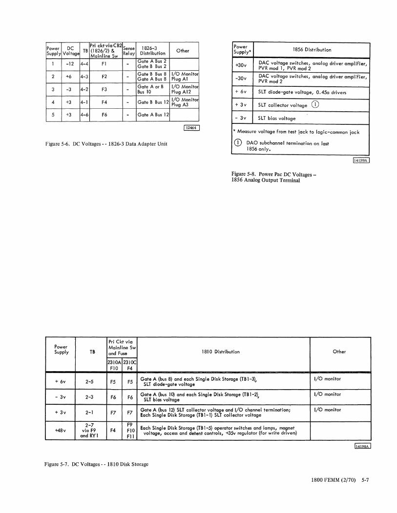
Power DC Pri ckt via CB2 Sense 1826-3 Supply VoltagE TB (1826/2) & Relay Distribution Other
Mainline Sw
Power 1856 Distribution Supply*
1 -12 4-4 Fl - Gate A Bus 2 Gate B Bus 2 +30v DAC voltage switches, analog driver amplifier,
PVR mod I, PVR mod 2
2 +6 4-3 F2 - Gate B Bus 8 I/o Monitor Gote A Bus 8 Plug Al -30v DAC voltage switches, analog driver amplifier,
PVR mod 2
3 -3 4-2 F3 - Gate A or B I/o Monitor Bus 10 Plug A12 + 6v SLT diode-gate voltage, 0.45a drivers
4 +3 4-1 F4 - Gate B Bus 12 I/o Manito Plug A3 + 3v SLT collector voltage CD
5 +3 4-6 F6 - Gate A Bus 12 - 3v SLT bias voltage
* Measure voltage from test jack to logic-common jack
Figure 5-6. DC Voltages - - 1826-3 Data Adapter Unit CD DAO subchannel termination on last
Pri Ckt via Power Mainline Sw Supply TB and Fuse
2310A 2310C FlO F4
+ 6v 2-5 F5 F5
- 3v 2-3 F6 F6
+ 3v 2-1 F7 F7
2-7 F9 +48 v via F9 F4 FlO
and RYI Fll
1856 only.
Figure 5-8. Power Pac DC Voltages-1856 Analog Output Terminal
1810 Distribution Other
Gate A (bus 8) and each Single Disk Storage (TB 1-3), I/o monitor SLT diode-gate voltage
Gate A (bus 10) and each Single Disk Storage (TBI-2) SLT bias voltage '
I/O monitor
Gate A (bus 12) SLT collector voltage and I/O channel termination; I/O monitor Each Single Disk Storage (TB 1-1) SLT collector voltage
Each Single Disk Storage (TB 1-5) operator switches and lamps, magnet voltage, access and detent controls, +35v regulator (for write drivers)
Figure 5-7. DC Voltages--181O Disk Storage
1800 FEMM (2/70) 5-7
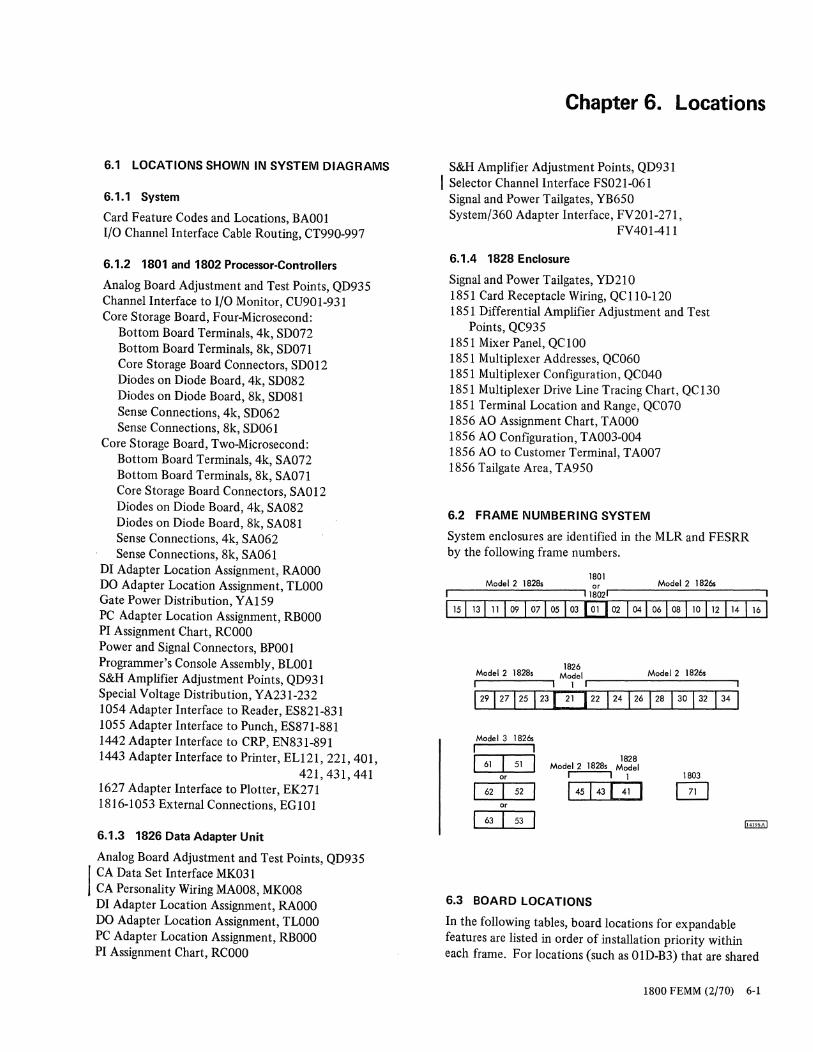
6.1 LOCATIONS SHOWN IN SYSTEM DIAGRAMS
6.1.1 System
Card Feature Codes and Locations, BAOOI I/O Channel Interface Cable Routing, CT990-997
6.1.2 1801 and 1802 Processor-Controllers
Analog Board Adjustment and Test Points, QD935 Channel Interface to I/O Monitor, CU901-931 Core Storage Board, Four-Microsecond:
Bottom Board Terminals, 4k, SDOn Bottom Board Terminals, 8k, SD071 Core Storage Board Connectors, SD012 Diodes on Diode Board, 4k, SD082 Diodes on Diode Board, 8k, SD081 Sense Connections, 4k, SD062 Sense Connections, 8k, SD061
Core Storage Board, Two-Microsecond: Bottom Board Terminals, 4k, SAOn Bottom Board Terminals, 8k, SA071 Core Storage Board Connectors, SA012 Diodes on Diode Board, 4k, SA082 Diodes on Diode Board, 8k, SA081 Sense Connections, 4k, SA062 Sense Connections, 8k, SA061
DI Adapter Location Assignment, RAOOO DO Adapter Location Assignment, TLOOO Gate Power Distribution, Y A159 PC Adapter Location Assignment, RBOOO PI Assignment Chart, RCOOO Power and Signal Connectors, BPOOI Programmer's Console Assembly, BLOOI S&H Amplifier Adjustment Points, QD931 Special Voltage Distribution, YA231-232 1054 Adapter Interface to Reader, ES821-831 1055 Adapter Interface to Punch, ES871-881 1442 Adapter Interface to CRP, EN831-891 1443 Adapter Interface to Printer, EL121, 221, 401,
421,431,441 1627 Adapter Interface to Plotter, EK271 1816-1053 External Connections, EG 101
6.1.3 1826 Data Adapter Unit
Analog Board Adjustment and Test Points, QD935
I CA Data Set Interface MK031 CA Personality Wiring MA008, MK008 DI Adapter Location Assignment, RAOOO DO Adapter Location Assignment, TLOOO PC Adapter Location Assignment, RBOOO PI Assignment Chart, RCOOO
Chapter 6. Locations
S&H Amplifier Adjustment Points, QD931 I Selector Channel Interface FS021-061
Signal and Power Tailgates, YB650 System/360 Adapter Interface, FV201-271,
FV401-411
6.1.4 1828 Enclosure
Signal and Power Tailgates, YD210 1851 Card Receptacle Wiring, QC 110-120 1851 Differential Amplifier Adjustment and Test
Points, QC935 1851 Mixer Panel, QC 100 1851 Multiplexer Addresses, QC060 1851 Multiplexer Configuration, QC040 1851 Multiplexer Drive Line Tracing Chart, QC130 1851 Terminal Location and Range, QC070 1856 AO Assignment Chart, TAOOO 1856 AO Configuration, TA003-004 1856 AO to Customer Terminal, TA007 1856 Tailgate Area, TA950
6.2 FRAME NUMBERING SYSTEM
System enclosures are identified in the MLR and FESRR by the follOWing frame numbers.
Model 2 1828. 1801 Model 2 18260 I 118~1 I
115113111 I 09 I 071 05 I 03 I 01 I 02 I 041 061 08 110 112 114 116 I
Model 3 18260 I I I 61 I 51 I
or
62 I 52 or
63 I 53
1828 Model 2 1828. Model
I I 1
1 45143 I 41 I
6.3 BOARD LOCATIONS
Model 2 18260
1803
~
In the following tables, board locations for expandable features are listed in order of installation priority within each frame. For locations (such as 0ID-B3) that are shared
1800 FEMM (2/70) 6-1
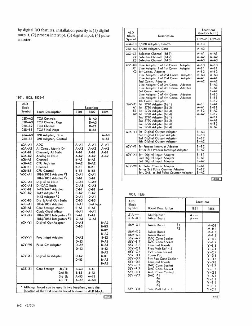
by digital I/O features, installation priority is (1) digital output, (2) process interrupt, (3) digital input, (4) pulse counter.
1801, 1802, 1826-1
ALD Block Locations Symbol Board Description 1801 1802 1826
02D-A2 TCU Controls D-A2 02D-A3 TCU Clocks, Regs D-A3 02D-B2 TCU Channel D-B2 02D-B3 TCU Final Amps D-B3
26A-A3 360 Adapter, Data A-A3 26A-B3 360 Adapter, Control A-B3
6OA-Al ADC A-AI A-AI A-AI 6OA-A2 AI Comp, Matrix Dr A-A2 A-A2 A-A2 6OA-BI Channel, AI Basic A-BI A-Bl A-Bl 6OA-B2 Analog In Basic A-B2 A-B2 A-B2 60B-AI Channel B-Al B-Al 6OB-A2 CPU Registers B-A2 B-A2 6OB-BI Channel B-Bl B-BI 60B-B2 CPU Control, B-B2 B-B2
*6OC-AI 1816/1053 Adapter 'I C-AI C-AI 1816/1053 Adapter #2 D-BI D-Bl
6OC-A2 Digital In Basic C-A2 C-A2 6OC-A3 DI-DAO Basic C-A3 C-A3 6OC-B1 1443/1627 Adapter C-Bl C-BI <-"
*6OC-B2 1442 Adapter 'I C-B2 C-B2 1442 Adapter '2 D-Al D-AI
6OC-B3 Dig & Anal Out Basic C-B3 C-B3 6OD-AI 1054/1055 Adapter D-Al D-AI .. ... 6OE-AI Core Storage Mixer E-Al E-AI 6OH-Al Cycle-Steal Mixer H-AI H-AI 6OX-X5 18i 6/1 053 Integrators #i F-Al F-AI
1816/1053 Integrators #2 G-AI G-AI 6OX-YI Digital Out Adapter D-A3 B-A3
0-83 B-B3 B-B2 B-A2
6OY-Vl Proc Intrpt Adapter D-A2 B-82 D-B3 B-A2
6OY-WI Pu Ise C tr Adapter D-A2 B-AI D-B3 B-B2
B-A2 6OY-XI Digital In Adapter 0-82 B-BI
0-83 B-Al B-A2
63Z-Z1 Core Storage 4k/8k B-A3 B-A3 2nd 8k B-83 B-B3 3rd 8k A-B3 A-B3 4th 8k A-A3 A-A3
* Although board can be used In two locations, only the location of the first adapter board Is shown In ALD block.
6-2 (2/70)
Locations ALD (factory build) Block Description
Symbol 1826-2 1826-3
26A-B 3 S/360 Adapter, Control A-B3
26A-A3 S/36O Adapter, Data A-A3
26Z-Z1 Selector Channel (Bd I) A-AI A-AI Z2 Selector Channel (Bd 2) A-A2 A-A2 Z3 Selector Channel (Bd 3) A-A3 A-A3
26Z-X3 Li ne Adapter 0 of 1st Comm Adapter A-B3 A-B3 XI Line Adapter I of 1st Comm Adapter A-B I A-B I X2 1st Comm. Adapter A-B2 A-B2
Line Adapter 0 of 2nd Comm Adapter A-A3 A-A3 Line Adapter I of 2nd Comm Adapter A-AI A-AI 2nd Comm. Adapter A-A2 A-A2 Line Adapter 0 of 3rd Comm Adapter B-A3 Li ne Adapter I of 3rd Comm Adapter B-AI 3rd Comm. Adapter B-A2 Line Adapter 0 of 4th Comm Adapter B -B 3 Li ne Adapter I of 4th Comm Adapter B -B I 4th Comm Adapter B -B2
26Y-BI 1st 2790 Adapter (Bd 1) A-B I B -AI Al 1 st 2790 Adapter (Bd 2) A-AI B -B I B2 1st 2790 Adapter (Bd 3) A-B2 B-A2 A2 1st 2790 Adapter (Bd 4) A-A2 B -B 2
2nd 2790 Adapter (Bd 1) A-B 1 2nd 2790 Adapter (Bd 2) A-AI 2nd 2790 Adapter (Bd 3) A-B2 2nd 2790 Adapter (Bd 4) A-A2
6OX-YI 1st Digital Output Adapter B-A3 2nd Digital Output Adapter B -B3 3rd Digital Output Adapter B -B 2 4th Digital Output Adapter B-A2
60Y-VI I st Process I nterrupt Adapter B -B 2 I st or 2nd Process I nterrupt Adapter B-A2
60Y-XI 1st Digital Input Adapter B -B I 2nd Digital Input Adapter B-AI 3rd Digital Input Adapter B-A2
60Y-WI 1st Pulse Counter Adapter B-AI 1st or 2nd Pulse Counter Adapter B -B 2 1st, 2nd I or 3rd Pu I se Counter Adapter B-A2
112451 I
1851, 1856
ALD Locations Block Symbol Board Description 1851 1856
51A --- Multiplexer A---51A-X3 Mixer Board A---
56M-X 1 Mixer Board #1 M-G8 #2 M-H8
56M-X2 Mixer Board M-E 8 56M-X3 Mixer Board M-F 8 56Y-A7 DAC Conn Socket Y-A7 56Y -B 7 DAC Conn Socket Y-B 7 56Y -B 8 Termina I Boards Y-B 8 56Y -C 1 Prec Volt Ref - 2 Y-C I 56Y -C7 PVR Conn Socket Y-C7 56Y -D I Power Pac Y-D 1 56Y -D 7 Pwr Pac Conn Socket Y-D7 56Y -D8 Terminal Boards Y-D8 56Y -E 7 DAC Conn Socket Y-E 7 56Y -F 7 DAC Conn Socket Y-F 7 56Y-GI Anlg Chan Control Y-GI 56Y-Y7 DAC #1 V-A I
#2 Y-B I #3 Y-E I #4 Y-F I
56Y -Y8 Prec Volt Ref - I Y-C I
6.4 WIRED LOGIC (WL) JUMPERING
6.4.1 Interrupt, Cycle Steal, IPL
Analog Input and Comparator, QD041, QD042, QD991 Cycle Steal (Channel Board), BC101, CU991, CU995 Cycle Steal (Mixer Board), BCl01, CT997
I Communications Adapter, MA008, MB997 Digital and Analog Output, PBOOO, PA991 Digital Input, PDOOO, PA991 Interrupt (Additional Levels), BC150, CU995 Interval Timers and Console, BC150, CU991, CU995
I Selector Channel, FSO 11, FSO 13 System/360 Adapter, FV001, FZ991 Tape Control Unit, GAlli, GB991 1053-1816 Printer and Printer-KB, EA001, EA991 1054-1055 Paper Tape Reader-Punch, ES001, ES992 1442 Card Read Punch, EN001, EN991 1443 Printer, EJ005, EJ991 1627 Plotter, EJ001, EJ991 1810A Disk Storage, FA001, FA991, FA992 1810B Disk Storage, FC001, FC991
6.4.2 Other
AO Addressing, TAOO 1, T A051 AO Optional Features, TA001, TA661, TA631, TA991 Core Storage Module Selection, 2-ILS, SA111 Core Storage Module Selection, 4-lLs, SD331
I Communications Adapter, MA008, MB997, MB998, MB999 DI Group Addressing, RA002, RA021 DI High-Speed Voltage Input, RAlll-821 DO Control, TL001, TL051 DO Group Addressing, TL001, TL1lO, TL120, TL130,
TL140 Interval Timer (Time Selection), CU991
I Line Adapter, MK008, MM998, MM999 PC Coupler, RB991 PC Group Addressing, RB005, RB021 PI High-Speed Input, RClll-821 PI ILSW Bit Jumpering, RC004, RC981 PI Level Decode Jumpering, RC002, RC981 PI Request Jumpering, RC001, RC991 System/360 Adapter Address Decode, FV005, FY101 System/360 Adapter Select-Bypass, FV005, FV251
I 2790 Adapter LA005, LC991
6.5 COMPONENT LOCATIONS INDEX
6.5.1 1801 and 1802 Processor-Controllers
Console switches and lamps are shown on BLOOl, BL005, and BL009. ALD page locations of other components are shown on YA700-710.
&
Fuses (Y AlOO)
F1 thru F36 F37 F38,F39
Relays (Y AlOO)
RY1 thru RY16 RY17 thru RY19 RY20 thru RY23
Contactors (YAl10)
K1 thruK4 K5
Circuit Breakers (Y AlOO)
CB1 thru CB4
Edge Connectors (YAl10)
EC1 thru EC12 EC15 thru EC20
Terminal Boards (Y Al10)
TB1 thru TB6 TB6B TB7 TB8 TB9 TBIO TBll TB12, TB13 TB14, TB15, TB16 TB17 TB18 thru TB20 TB21 TB22 TB23
6.5.2 1803 Core Storage Unit
Lamps CB Power on Neon Ready
Fuses
Figure 6-13 Figure 6-14 Figure 6-13
F1 through F7 Figure 6-14
Contactors
Kl K2
Figure 6-14 Figure 6-14
Figure 6-3, 6-4 Figure 6-1 Figure 6-2
Figure 6-5 Figure 6-6 Figure 6-5
Figure 6-3, 6-4 Figure 6-4
Figure 6-3, 6-4
Figure 6-5 Figure 6-1
Figure 6-3, 6-4 Figure 6-4 Figure 6-6 Figure 6-5 Figure 6-3, 6-4 Figure 6-1 Figure 6-2 Figure 6-6 BL001 Figure 6-1 Figure 6-2 Figure 6-3 Figure 6-2 Figure 6-1
YS210 YS210 YS240
YS210
YS210 YS240
1800 FEMM (2/70) 6-3
Edge Connectors
ECI and 2
Mainline CB
Terminal Board
TBI and 2 TB4
Figure 6-15
Figure 6-14
Figure 6-14 Figure 6-15
YS210
YS210 YS240
6.5.3 1826 Data Adapter Unit, Models 1 and 2
Fuses
Fl thruFlO
Relays
RYI thru RY3 RY4, RY5
Edge Connectors
ECI
Terminal Boards
TBI thru TB3 TB4, TBS TB6
6.5.4 1826-3 Data Adapter Unit
Lamps
CB Figure 6-23 Power On N.eon Figure 6-24
Fuses (YB110)
F 1 through F7 Figure 6-24
Relays (None)
Contactors (None)
Circuit Breakers (None)
Main Line Switch Figure 6-23
Edge Connector
ECI
Terminal Boards
TBI TB2
TB4
6-4 (2/70)
Figure 6-25
Figure 6-24 Figure 6-24
Figure 6-25
Figure 6-18
Figure 6-19 Figure 6-18
Figure 6-18
Figure 6-18 Figure 6-19 Figure 6-18
YB220 YB210
YB210
YB210 YB21O, YB220 and YB2S0 YB240
6.5.5 1828 Enclosure
Fuses
Fl, F2 Figure 2-28
Terminal Boards
TBl, TB2 TB4
YD210 Figure 2-28
6.6 LOCATIONS FIGURE LISTING
Figure 6-1. Figure 6-2. Figure 6-3.
Figure 6-4.
Figure 6-S. Figure 6-6. Figure 6-7. Figure 6-8. Figure 6-9. Figure 6-10. Figure 6-11. Figure 6-12. Figure 6-13. Figure 6-14. Figure 6-1S. Figure 6-16. Figure 6-17. Figure 6-18.
Figure 6-19. Figure 6-20. Figure 6-21.
Figure 6-22. Figure 6-23. Figure 6-24. Figure 6-2S. Figure 6-26. Figure 6-27.
Figure 6-28. Figure 6-29. Figure 6-30. Figure 6-31.
1801/1802 Processor-Controller (Front) 1801/1802 Processor-Controller (Rear) 1801/1802 Power Sequence Assembly (60-Hz) 1801/1802 Power Sequence Assembly (50-Hz) 1801/1802 Relay Panel A 1801/1802 DC Distribution Assembly 1801 Customer Termination Area Customer Terminal Block (Digital I/O) Fault Protection Boards (Digital I/O) 1801 SLT Board Locations 1802 SLT Board Locations 1803 Core Storage Unit (Front) 1803 Core Storage Unit (Rear) 1803 AC Power Distribution Assembly 1803 DC Power Panel 1803 SLT Board Locations 1826 Data Adapter Unit (Mod 1 and 2) 1826 Power Sequence Assembly (Mod 1 and 2) 1826 DC Power Panel (Mod 1 and 2) 1826 SLT Board Locations (Mod 1) 1826 Customer Termination Area
1826 Data Adapter Unit, Model 3 (Front) 1826 Data Adapter Unit, Model 3 (Rear) 1826-3 Power Distribution Assembly 1826-3 DC Power Panel 1826-2 SLT Board Locations 1826-3 SLT Board Locations
1828 Enclosure 1851 Multiplexer Terminal (Front) 1856 Analog Output Terminal (Front) 18S6 AO Board Coordinates
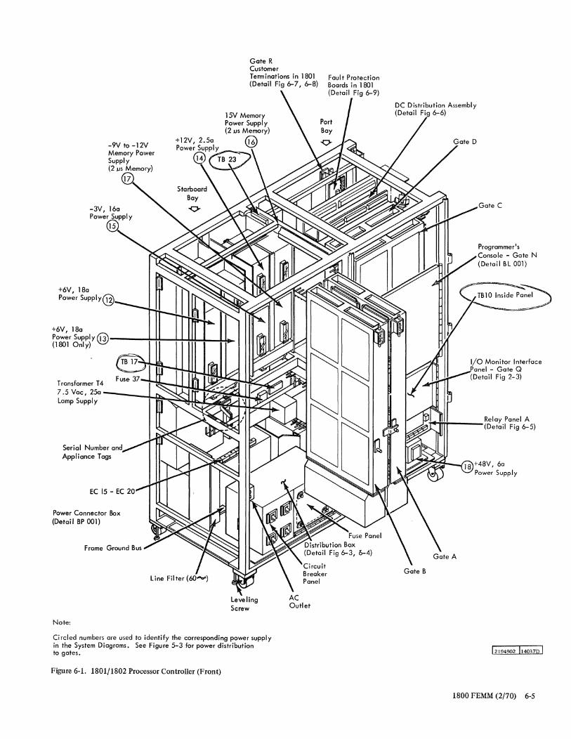
-9Vto-12V
+6V, 180 Power Suppl y@
Gate R Customer Terminations in 1801 (Detail Fig 6-7, 6-8)
+6V, 180 Power Supply @----+*-++-!#--4--..&..J~ (1801 Only)
Transformer T 4 ~~~:::t~f~~~iJU: 7.5 Voc, 250--__ -+-!r..~::s~ Lamp Supply
Serial Number and App Ii once Togs
Power Connector Box (Detail BP 001)
Frame Ground Bus
Note:
Leveling Screw
Circled numbers are used to identify the corresponding power supply in the System Diagrams. See Figure 5-3 for power distribution to gates.
Figure 6-1. 1801/1802 Processor Controller (Front)
Foul t Protection Boards in 1801 (Detail Fig 6-9)
DC Distribution Assembly (Detail Fig 6-6)
J::-,+liH-l-____ Relay Panel A (Detail Fig 6-5)
12194902 114037D 1
1800 FEMM (2/70) 6-5

Programmer's Console - Gote N (Detail BL 001)
Relay Panel A (Detai I Fig. 6-5)
Gate T
Port Tower liP"
Signal Tailgate ___ ...,..p:~~~~::-.,..~ (Detail BP 001)
NOTE:
Gate G Gate F 1053/1816 1053/1816 Expander Basic (Integrators Mounted on Card Connectors Inside)
Circled numbers are used to identify the carresponding power supply in the System Diagrams. See Figure 5-3 for power distributian to gates.
Figure 6-2. 1801/1802 Processor-Controller (Rear)
6-6 (2/70)
Starboard Tower
leol Custarner Termination Area (Detai Is Fig. 6-7, 6-8)
+36v,3a Power Supply o (leol) -12v,2.5a Pawer Supply (1802)
+3v, 12a Power Supply
+3v, 160 Power Supply
+3v, 160 Power Supply
+6v, ISo Power Supply
+6v, 180 Power Supply
-JOv, 20 Power Supply
+JOv,2a Power Supply
0-3v, Power Failure Protec t Supp I y
+12v,5a Power Supply
+3v, 160 Power Supply
12194902 1 14038D I
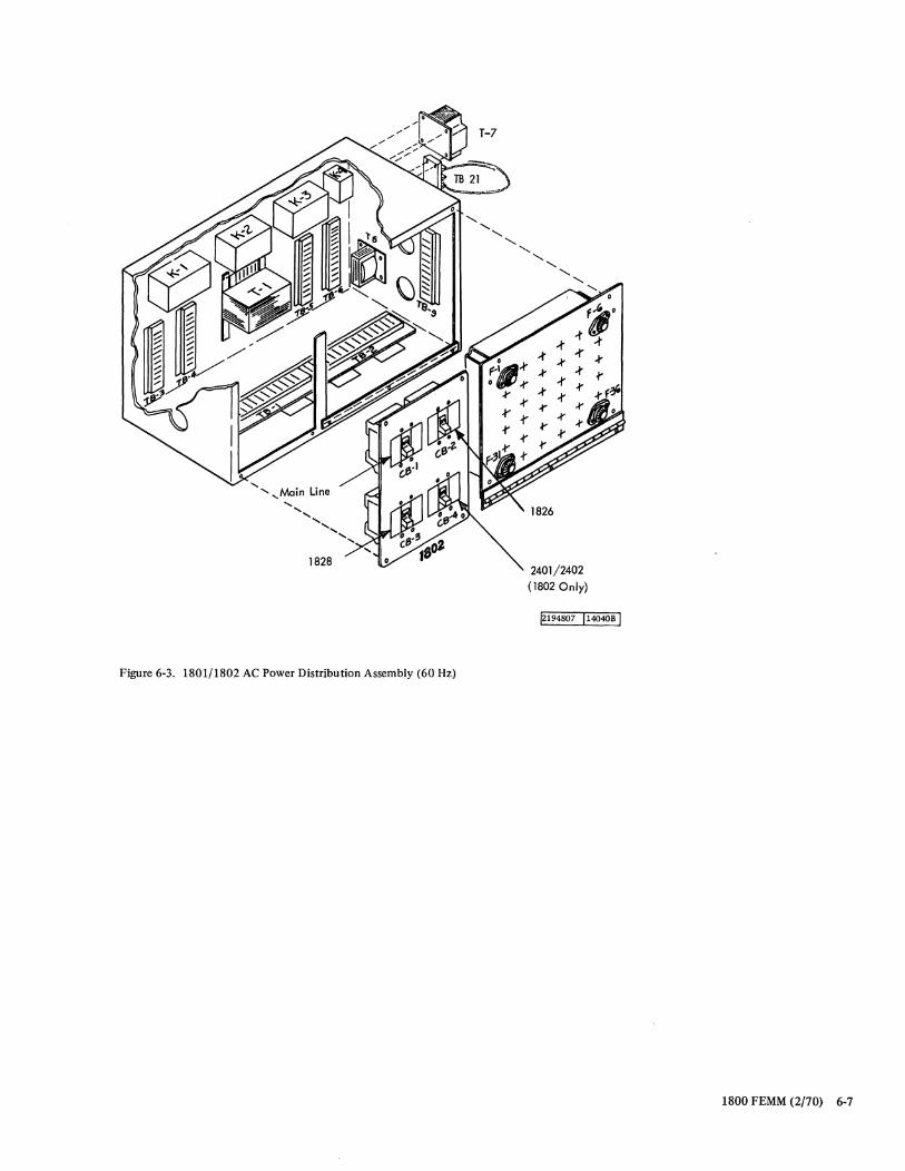
T-7
1828
Figure 6-3. 1801/1802 AC Power Distribution Assembly (60 Hz)
11" -t • -t -t -t .... -r .... .... ....
of -t .... of
.f'"
2401/2402 (1802 Only)
12194807 1140408 1
1800 FEMM (2/70) 6-7
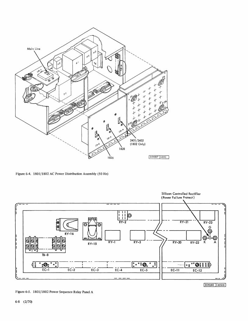
" "
Figure 6-4. 1801/1802 AC Power Distribution Assembly (50 Hz)
/ I
I I
I \.- --
RY-IS
TB-8
Figure 6-5. 1801/1802 Power Sequence Relay Panel A
6-8 (2/70)
RY-l
12194827 114131
Si !icon Controlled Rectifier (Power Foi lure Protect)
D ___ _ RY-3
1: 00 :00 00:1 EC-4 EC-5
---"'\
RY-21 RY-23
G
D~ --"R"'"'y'---20::-0-- RY -22 K A
-----___ -_-_-1 0 g 00088 g gP
EC-ll EC::-12
I I
I I ,
-- -"
12195285 114050B 1
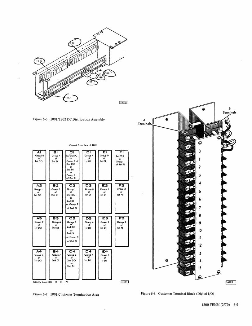
Figure 6-6. 1801/1802 DC Distribution Assembly
AI Group 0
of 1st DO
A2 Group 1
of 1st DO
A3 Group 2
of 1st DO
A4 Group 3
of 1st DO
BI Group 4
of 2nd 01
B2 Group 5
of 2nd 01
B3 Group 6
of 2nd 01
B4 Group 7
of 2nd 01
Viewed From Rear of '801
01 1st/2nd PC
or Group Oof 2nd DO
or 2nd 01
or Group I of 2nd PI
02 Group I
of 2nd DO
or 2nd 01
or Group 2
of 2nd PI
03 Gr~2
2nd DO
or 2nd 01
or Group 3
of 2nd PI
04 Group 3
of 2nd DO
or 2nd 01
01 Group 4
of 1st 01
02 Group 5
of 1st 01
03 Group 6
of 1st 01
04 G~t7
1st 01
Priority Seon: DO - PI - 01 - PC
Figure 6-7. 1801 Customer Termination Area
EI Group 0
of 1st 01
E2 Group I
of 1st 01
E3 Group 2
of 1st 01
E4 Group 3
of 1st 01
FI 1st PCA
or Group I of 1st PI
F2 Group 2
of 1st PI
F3 Group 3
of 1st PI
Temll nClIs",:!-
Figure 6-8. Customer Terminal Block (Digital I/O)
1800 FEMM (2/70) 6-9
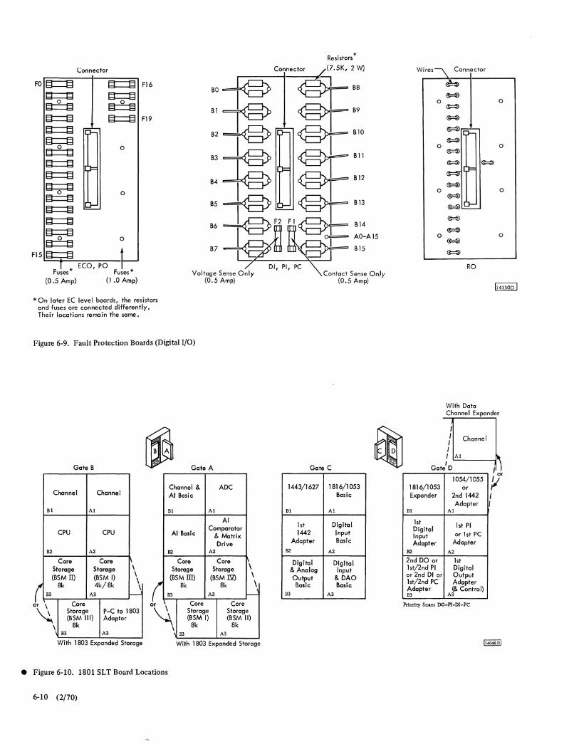
Resistors"
Connector
F16 M BB FO §:::::§ §::::§
~ §:::::::§ §::::§ §:::::§
~ §::::§
F19
o
~'"'1?;.5K' 2 ~ BO I
~ :~ ~ ~ ~ ::0
OJ I~ ~ ~BII B4 I ~BI2
§::::§
~ §::=:§ §:::::::§
~ §::::§
o
:: I ~ ~ F2 FI ~ ~l ::: B7 ~ c3: ;~;A1' ~ o
t ECO, PO I
F159
Fuses" (0.5 Amp)
Fuses" (1.0 Amp)
Voltage Sense Only (0.5 Amp)
"On later EC level boards, the resistors and fuses are connected differently. Their locations remain the same.
Figure 6-9. Fault Protection Boards (Digital I/O)
Gate B Gate A
Channel Channel Channel & AOC AI Basic
BI Al BI Al
AI
CPU CPU AI Basic Comparator
& Matrix Drive
B2 A2 B2 A2
Core Core Care Core Storage Storage \ (BSMID (BSM I) \
\ ( B3 Bk
4k/Bk \ A3 ---'
Core o 0
Storage Storage (BSMill) (BSM BZ)
( B3
8k Bk A3
Core Core
\ \ \
-r \
~ Storage P-C to lB03
r \
~ Storage Storage
(BSM III) Adapter
\ Bk B3 A3
(BSM I) (BSM II)
\ Bk Bk
B3 A3
W,th 1 B03 Expanded Storage With 1 B03 Expanded Storage
• Figure 6-10. 1801 SLT Board Locations
6-10 (2/10)
01, PI, PC Contact Sense Only
(0.5 Amp)
Gate C
1443/1627 lB16/1053 Basic
BI Al
lst Olgltol 1442 Input
Adapter Basic
B2 A2
~igital ~igital & Analog Input Output & OAO Basic Basic
B3 A3
Wires~ Connector
o
o
o
o
~
~
~
~
~,.::~
~
~J=~ ~
~
~
~.2::....
RO
With Data
o
o
o
o
Channe I Expander
I f Channel , I Al
Gate'O
1054/1055 lB16/1053 or Expander 2nd 1442
Adapter BI Al
1st lst PI ~igital Input or lst PC Adapter Adapter
B2 A2
2nd DO or lst 1st/2nd PI Digital or 2nd 01 or Output 1st/2nd PC Adapter Adapter (& Control) B3 A3
Priority Scan: DO-P1-DI-PC
I
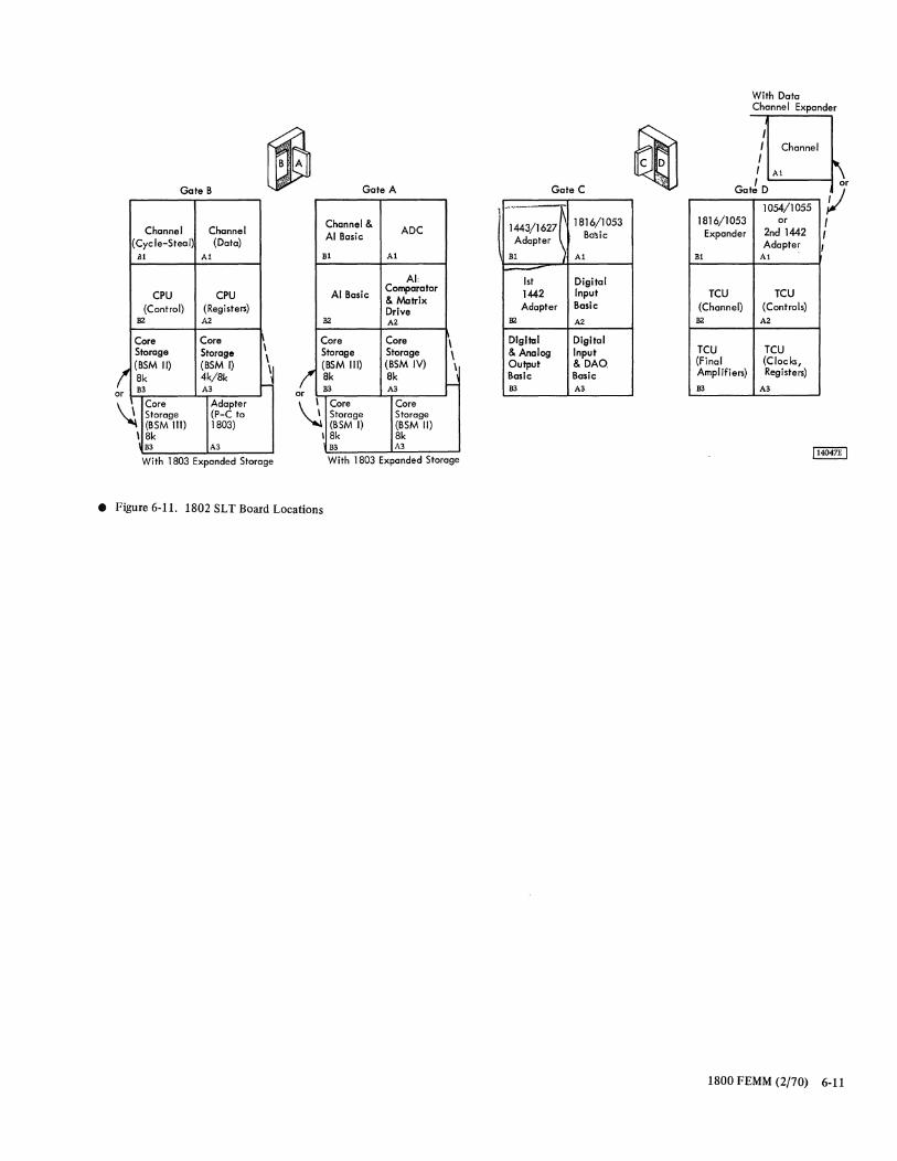
Gate B Gate A
Channel Channel (Cyc le-Stea I) (Data)
Channel & ADC
AI Basic
81 Al 81 Al
AI:
CPU CPU (Control) (Registers)
AI Basic Comparator & Matrix Drive
BZ A2 BZ A2
Core Core \ Storage Storage \
! (BSM II) (BSM I)
~ 8k 4k/8k B3 A3 I-
or a
Core Core \ Storage Storage \
( (SSM III) (BSM IV) \ 8k 8k B3 A3 I-
~ Core Adapter Storage (P-C to (8SM III) 1803) ~
Core Core Storage Storage (BSM I) (8SM II)
\ 8k , 8k 8k B3 A3 B3 A3
With 1803 Expanded Storage With 1803 Expanded Storage
• Figure 6-11. 1802 SLT Board Locations
Gate C
-1443/16271 1816/1053
Adapter 8a1;ic
81 Al - 1st Digitol 1442 Input Adapter Basic
BZ A2
Digital Digital & Analog Input Output & DAO, Basic Basic B3 A3
With Data Channel Expander
I I Channel I I Al
Gat~ 0
1054/1055 1816/1053 or
Expander 2nd 1442 I Adapte~ I
81 Al
TCU TCU (Channel) (Controls)
BZ A2
TCU TCU (Final (Clocks, Amplifiers) Registers)
53 A3
1800 FEMM (2/70) 6-11
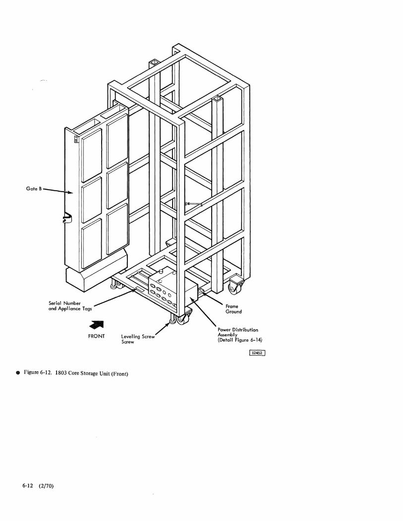
Gate B
Serial Number and Appl iance Tags
FRONT Leveling Screw Screw
• Figure 6-12. 1803 Core Storage Unit (Front)
6-12 (2/70)
Pawer Distribution Assembly (Detail Figure 6-14)
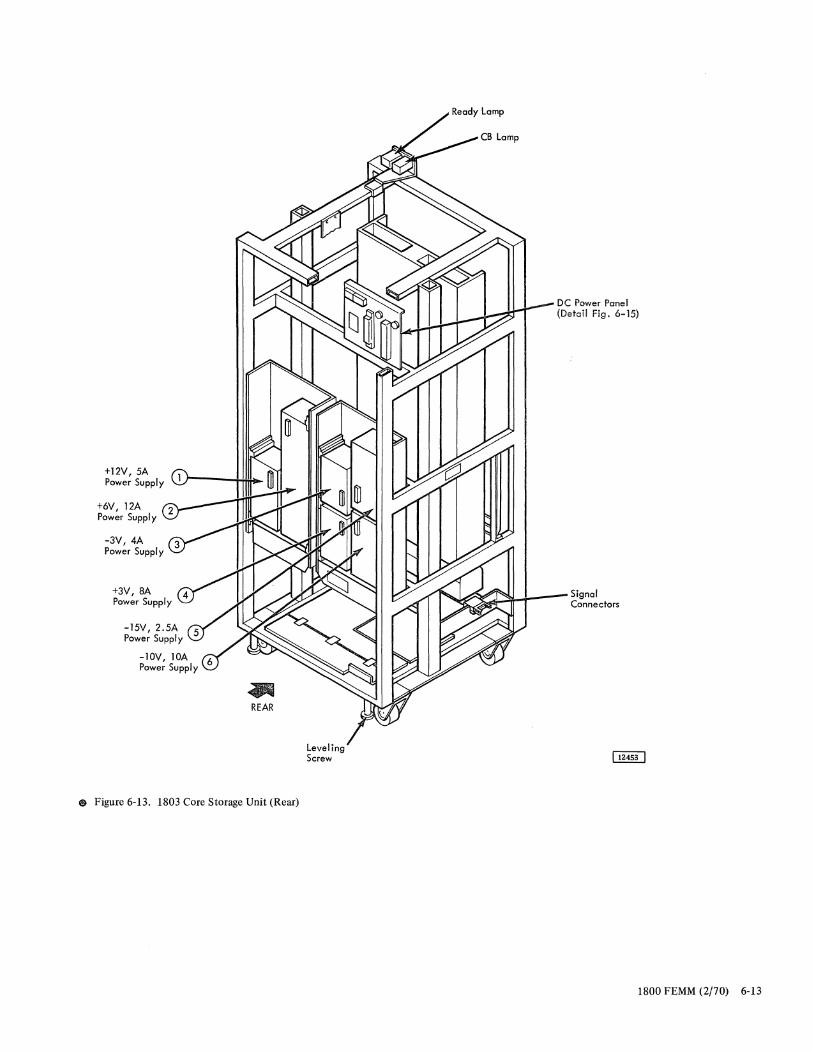
+12V,5A Power Supply
+6V, 12A 2 Power Supply
+3V,8A Power Supply
~ REAR
f) Figure 6-13. 1803 Core Storage Unit (Rear)
Leveling Screw
DC Power Panel (Detail Fig. 6- 15)
Signal ..::ll:l-i ..... -- Connectors
1800 FEMM (2/70) 6-13
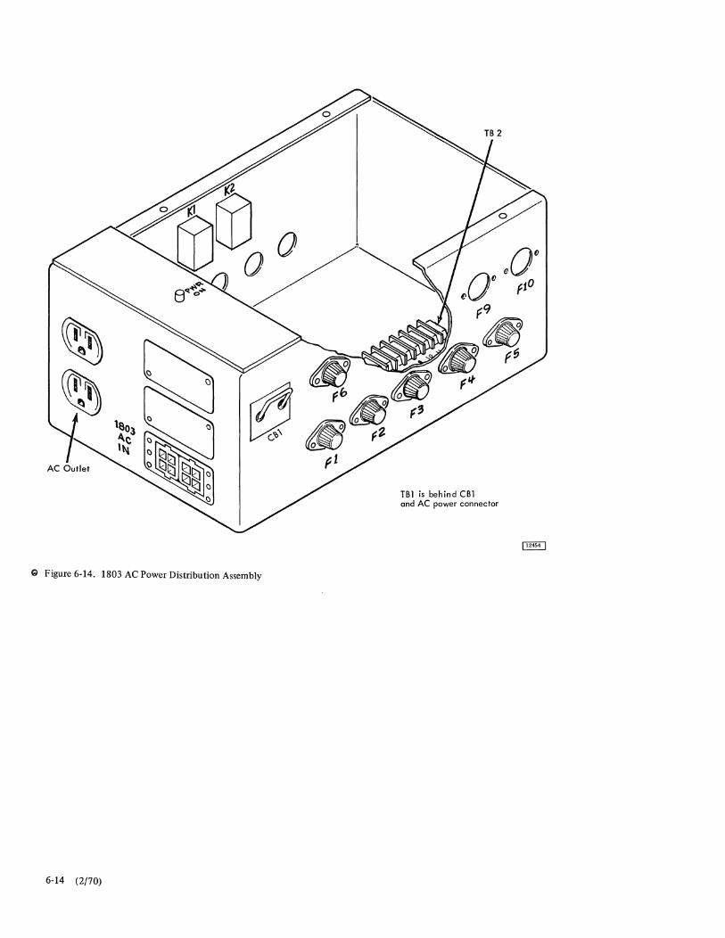
@ FO 19ure 6-14. 1803
6-14 (2/70)
AC Power DO ° lstnbution A ssembly
~~~ ~cbehind CBl power connector
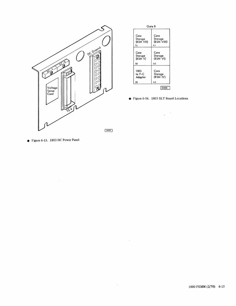
Gate B
Core Core Storage (BSM VII)
Storage (BSM VIII)
81 Al
Core Core Storage Storage (BSM V) (BSM Vi)
B2 A2
1803 Core to P-C Storage Adopter (BSM IV)
B3 A3
• Figure 6-16. 1803 SLT Board Locations
• Figure 6-15. 1803 DC Power Panel
1800 FEMM (2/70) 6-15
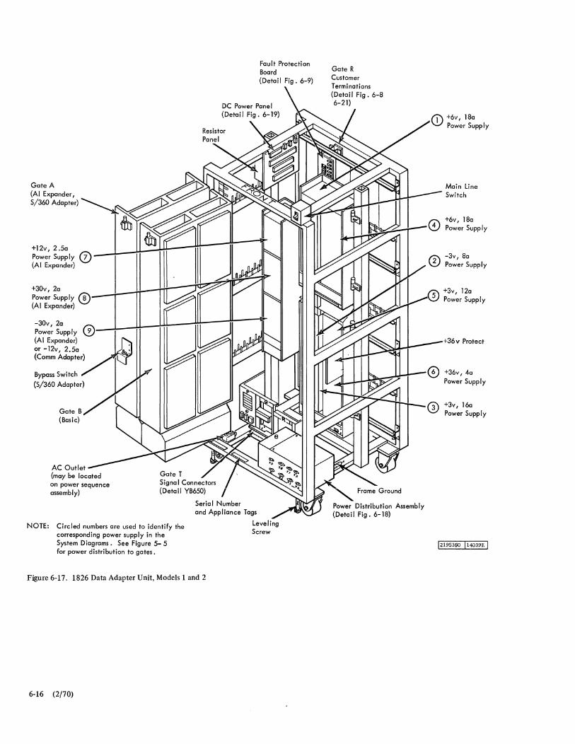
+12v,2,5a 0 Power Supply 7 (AI Expander)
+30v,2a Power Supply ® (AI Expander)
Gate B (Basic)
AC Outlet (may be located on power sequence assembly)
Gate T Signa I Connectors (Detail YB650)
Serial Number
Fau I t Protecti on Board (Detail Fig, 6-9)
and Appliance Tags
NOTE: 'd t'fy the Circled numbers are used to ,I e~ 1
corresponding power sUPF~ly In ; e5 Stem Diagrams, See Igure -f: power distribution to gates,
U 't Models 1 and 2 1826 Data Adapter m, Figure 6-17,
6-16 (2/70)
Leveling Screw
Gate R
Frame Ground
Power Distribution Assembly (Detail Fig, 6-18)
CD
+6v, 18a Power Supply
+3"6 v Protect
+36v,4a Power Supply
+3v, 160 Power Supply
12195360 1 14039E 1
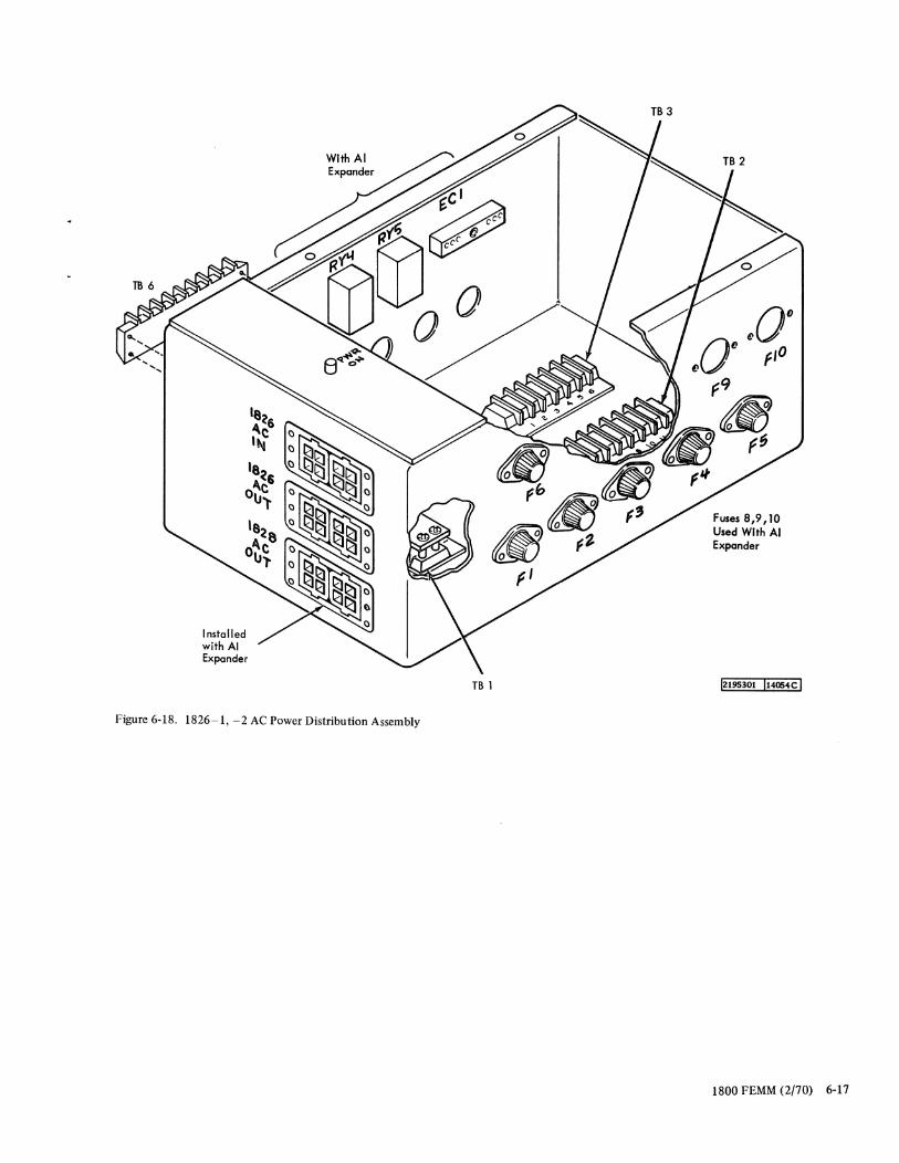
Installed with AI Expander
F JgUre 6-18. 1826 -1,-2ACP
WIth AI Expander
ower Distribu . tion Assembly
TB 1
Fuses 8,9,10 Used WIth AI Expander
12195301 114 054cl
1800 FEMM (2/7 0) 6-17
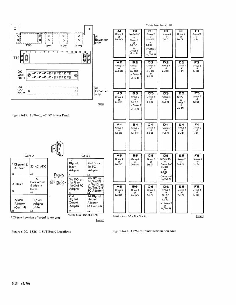
o
DC ,------- ----- ---, Gnd 10 0 I No.2 L __________________ J
Figure 6-19. 1826-1, -2 DC Power Panel
]AI Expander only
]AI Expander only
Gate A Gate B
1st
* Channel & 20 KC ADC AI Basic
Digital 2nd DI or Input 1st PC Adapter Adapter
B1 A1 81 A1
AI
AI Basic Campara tar & Matrix Drive
B2 A2
3rd DO or 4th DO or
- 1st PI or 1st/2nd PI
1st/2nd PC or 3rd DI or
Adapter 1st/2nd/3rd PC Adapter
82 A2
5/360 5/360 Adapter Adapter (Control) (Data)
2nd 1st Digital Digital Output Output Adapter Adapter (& Control)
B3 A3 B3 A3
Priority Scan: DO-PI-DI-PC .. Channe I portion of board is not used
Figure 6-20. 1826-1 SLT Board Locations
6-18 (2/70)
AI Group 2
of 2nd DO
A2 Group 3
of 2nd DO
A3 Group a
of lst DO
A4 Group 1
of lstDO
AS Group 2
of lstDO
AS Group 3
of lstDO
BI lst/2nd PC
or Group 0
of 3rd DO
or Group 1 of lst PI
B2 Group 1
of 3rd DO
or Group 2
of lst PI
B3 Group 2
of 3rd DO
or Group 3
of lst PI
B4 Group 3
of 3rd DO
B5 Group 0
of 2nd DO
BS Group I
of 2nd DO
Vi ewed From Rear of 1826
CI Group 2
of 4th DO
3rd DI
or Group 3
of lst/2nd PI
C2 Group 3
of 4th DO
3rd DI
C3 Group 4
of 3rd DI
C4 Group 5
of 3rd DI
C5 Group 6
of 3rd DI
CS Group 7
of 3rd DI
01 Group 4
of 2nd DI
02 Group 5
of 2nd DI
03 Group 6
of 2nd DI
04 Group 7
of 2nd DI
05 st/2nd PC
or Group 0 of 4th DO
or 3rd DI
or Group 1 of lst/2nd PI
OS Group 1
of 4th DO
or 3rd DI
or Group 2 of
lst/2nd PI
Priority Seon: DO - PI - DI - PC
Figure 6-21. 1826 Customer Termination Area
EI Group 6
of lst DI
E2 Group 7
of lst DI
E3 lst PC
or Group 0
of 2nd DI
E4 Group 1
of 2nd DI
E5 Group 2
of 2nd DI
ES Group 3
of 2nd DI
FI Group 0
of lst DI
F2 Group 1
of 1st DI
F3 Group 2
of lst DI
F4 Group 3
of lst DI
F5 Group 4
of lst DI
FS Group 5
of lst DI
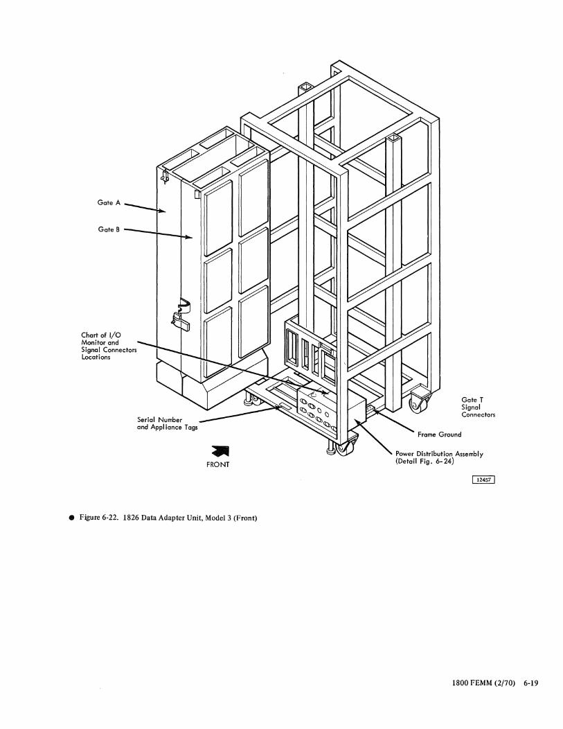
G ... A::t Gate B -,..-_J....~
Chart of I/O Monitor and Signal Connectors Locations
Serial Number and Appliance Tags
• FRONT
• Figure 6-22. 1826 Data Adapter Unit, Model 3 (Front)
Frame Ground
Gate T Signal Connectors
Power Distribution Assembly (Detail Fig. 6-24)
1800 FEMM (2/70) 6-19
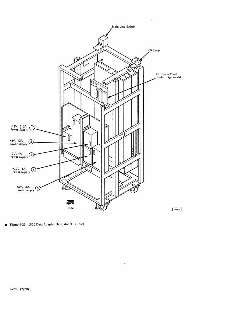
-12V,2.SA Power Supply
+6V,12A Power Supply
-3V,4A Power Supply
+3V,16A Power Supply
+3V, 16A Power Supply
~ REAR
• Figure 6-23. 1826 Data Adapter Unit, Model 3 (Rear)
6-20 (2/70)
Main Line Switch
DC Power Panel (Detail Fig. 6-25)
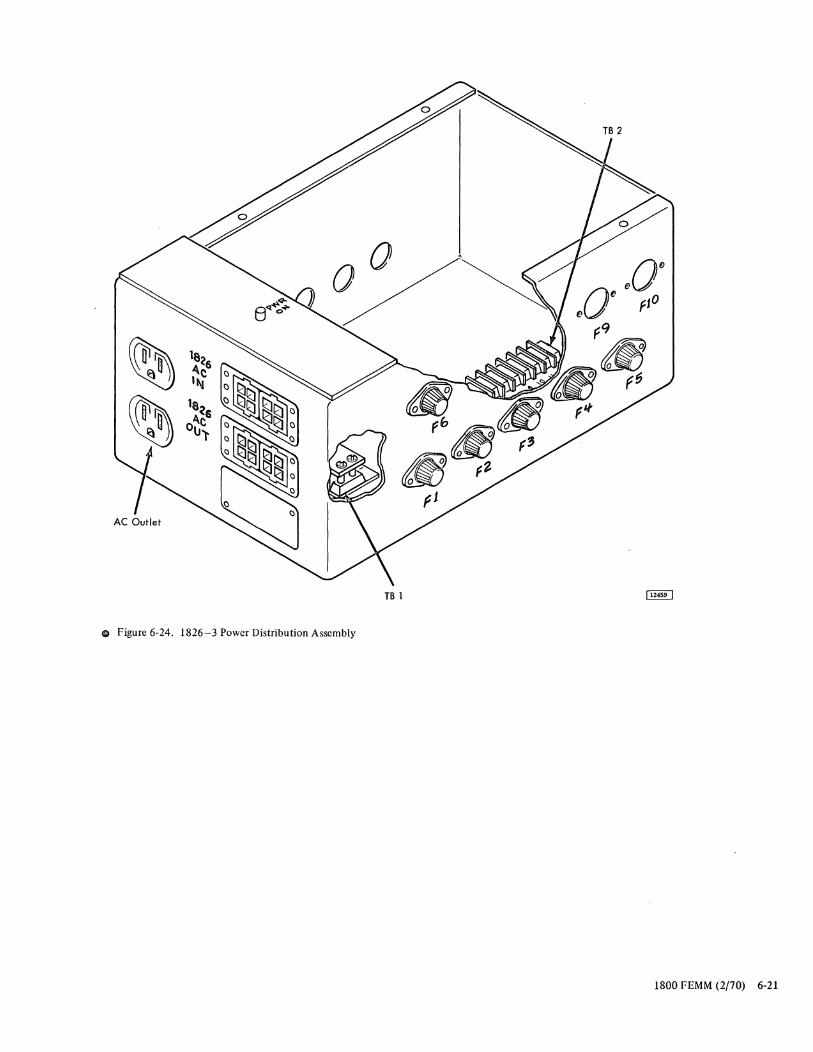
TB 1
iii> Figure 6-24. 1826-3 Power Distribution Assembly
1800 rEMM (2/70) 6-21
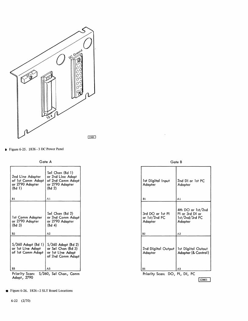
.. Figure 6-25. 1826-3 DC Power Panel
Gate A
Sel Chan (Bd 1) 2nd Line Adapter or 2nd Line Adapt of 1 st Comm Adapt of 2nd Comm Adapt or 2790 Adapter or 2790 Adapter (Bd 1) (Bd 2)
B1 A1
Sel Chan (Bd 2) 1 st Comm Adapter or 2nd Comm Adapt or 2790 Adapter or 2790 Adapter (Bd 3) (Bd 4)
B2 A2
S/360 Adapt (Bd 1) S/360 Adapt (Bd 2) or 1st Line Adapt or Sel Chan (Bd 3) of 1 st Comm Adapt or 1 st Line Adapt
of 2nd Comm Adapt
B3 A3
Priority Scan: S/360, Sel Chan, Comm Adapt, 2790
• Figure 6-26. 1826-2 SLT Board Locations
6-22 (2/70)
Gate B
1st Digital Input 2nd DI or 1st PC Adapter Adapter
B1 A1
4th DO or 1 st/2nd 3rd DO or 1st PI PI or 3rd DI or or 1 st /2nd PC 1 st/2nd/3rd PC Adapter Adapter
B2 A2
2nd Digital Output 1 st Digital Outout Adapter Adapter (& Control)
B3 A3
Priority Scan: DO, PI, DI, PC

Gate A
2nd Line Adapter Sel Chan (Bd 1) or 2nd Line Adapt of 1st Comm Adapt of 2nd Comm Adapt or 2nd 2790 Adapt
(Bd 1) or 2nd 2790 Adapt (Bd 2)
B1 A1
1 st Comm Adapter Sel Chan (Bd 2)
or 2nd 2790 Adapt or 2nd Comm Adapt
(Bd 3) or 2nd 2790 Adapt (Bd 4)
B2 A2
1st Line Adapter Sel Chan (Bd 3)
of 1 st Comm Adapt or 1 st Li ne Adapt of 2nd Comm Adapt
B3 A3
Priority Scan: Sel Chan, Comm Adapt, 2790
G Figure 6-27. 1826-3 SLT Board Locations
Gate B
2nd Line Adapter 2nd Li ne Adapter of 4th Comm Adapt of 3rd Comm Adapt or 1 st 2790 Adapt or 1 st 2790 Adapt (Bd 2) (Bd 1)
B1 A1
4th Comm Adapter 3rd Comm Adapter or 1 st 2790 Adapt (Bd 4)
or 1 st 2790 Adapt (Bd 3)
B2 A2
1st Line Adapter 1 st Line Adapter of 4th Comm Adapt of 3rd Comm Adapt
B3 A3
Priority Scan: Comm Adapt, 2790
112462 1
1800 FEMM (2/70) 6-23
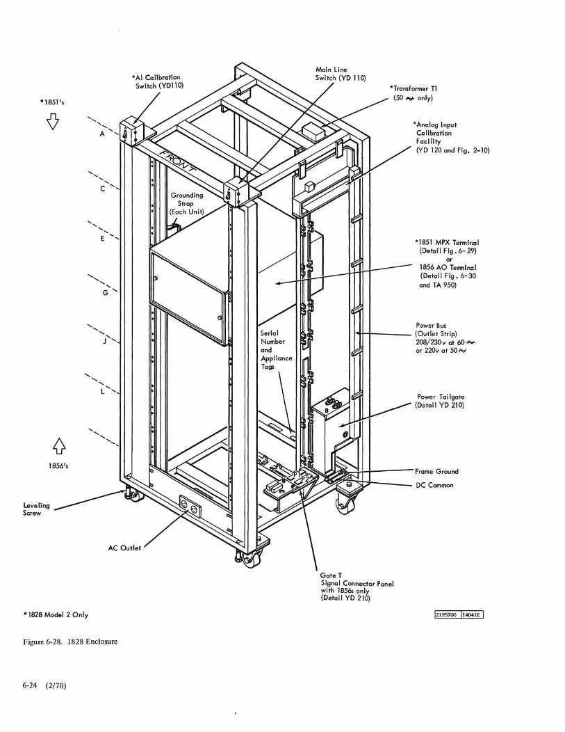
*1851'5
1856's
Leveling Screw
..........
* 1828 Model 2 Only
.......... J .....
Figure 6-28. 1828 Enclosure
6-24 (2/70)
*Transformer Tl (50 _ only)
*Analog Input Calibration Facility (YO 120 and Fig. 2-10)
*1851 MPX Terminal (Detail Fig. 6- 29)
or 1856 AO Terminal (Detail Fig. 6- 30 and TA 950)
Power Bus r'I1rt---- (Outlet Strip)
208/230v at 60.p"o. or 220v at 50,.."
Power Tailgate (Detai I YO 210)
~M.~~~~~~H-+----- Frame Ground
A~~~~~ ____ DC Common
Gate T Signal Connector Panel with 1856s only (Detail YO 210)
12195700 114041£ 1

Serial Number on Left Mounting Flange
Figure 6-29. 1851 Multiplexer Terminal (Front)
Analog Signal Cable Connectors
1 Amplifier Switch X Drive (MPX/R Only) 2 + First MPX Level Output, First Amplifier Input 4 - First MPX Level Output, First Amplifier Input 3 + Second MPX Level Output, Second Amplifier Input 6 - Second MPX Level Output, Second Amplifier Input 5 Analog Input to ADC
-----------~-----------05
04 06
Power Cable and Multiplexer Drive Cab I e Entry to A-X3 Mixer Board Mounted Inside Panel (Detail QC 100)
Multiplexer Drive Gate Connector from Mixer Board
Appliance Label
IHOO liEMM (2/70) 6-25
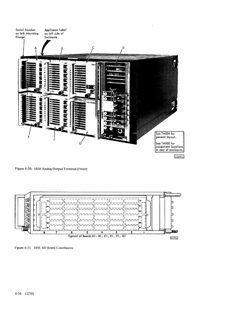
Serial Number on left Mounting Flange
Appliance Label on left side of Enclosure
F
Figure 6-30. 1856 Analog Output Terminal (Front)
Figure 6-31. 1856 AO Board Coordinates
6-26 (2/70)
See T A004 for general layout.
See T A 950 for component locations in rear of enclosure.
Appendixes
APPENDIX A. SPECIAL CIRCUITS Description PIN
This manual makes no distinction between special and Wire gripper 452529 standard circuits. Card offset extender (2) 452530
Probe tip (3) 452531 Pin aligner, card side 452535
APPENDIX B. WORLD TRADE Pin aligner, probe side 452536
World Trade differences are covered in their logical places Pin replacement kit 453158
in the manual. Card extender, 6 pak 452554 Card extender, 12 pak 452555 Light, trouble 450147
APPENDIX C. TOOLS AND TEST EQUIPMENT Manual cart (holds 36 volumes) Headset, telephone, sound power (if
453147
Shipped with System system has remote 1826 or 1828 units) (2) 460260 Adapter cord - 1 for each headset 2108538
Description PIN Adapter cord - 40 ft. (used to extend phone to System/360 console when
I/O Monitor - shipped with each 1801/1802 2194933 system has System/360 channel to
Analog input calibrate facility - shipped in channel adapter feature) 460261
1828 nearest the ADC N/A Adapter cord - used to connect two
Portable start/stop box - shipped with adapter cords (460261) together when
each 1801/1802 N/A System/360 console is over 40 feet
Digital output test cable (if system has away 2183478
DO feature) 2195696 Probe, plastic 453101
Digital input test card 2195669 Wire caddy 453106
Jumper assembly - core storage adj. 2182906 Thermometer 5392366
Cable assembly - differential scope leads- 2182907 Indicator removal tool 461163
DAC extender (if system has 1856) 2182700 Scope, Tektronix 453 (The 453 is the recommended scope for the 1800) 453047
Current probe 451213 Probe termination 451214 Simpson Meter Model 260 450497
Not Shipped with System Weston 901 DC Meter (must have 3V and 15V range) 460879
Description PIN Fluke Meter -(see 2.12.1) 453191 CE Indicator Latch Card 5801358
Hand wrap tool, 30 gauge or 452527 32 Inch SLT Jumpers 4203785 Power bit and sleeve (to be used with Core Jumper Block Removal Tool 2108860
existing wire wrapping guns) 453090 4" SLT Jumpers 452655 Deletion tool with check light 452533 CE Alignment screwdriver 460811 Wire stripper, 30 gauge 452528 Jumperboards 2242726
1800 FEMM (2/70) A-I
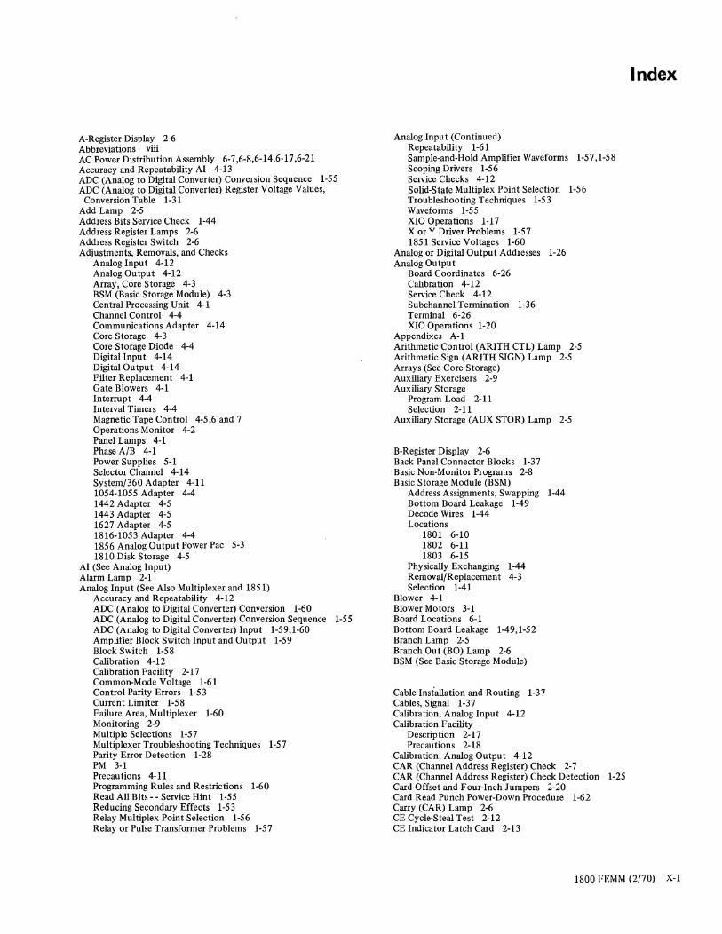
A-Register Display 2-6 Abbreviations viii AC Power Distribution Assembly 6-7,6-8,6-14,6-17,6-21 Accuracy and Repeatability AI 4-13 ADC (Analog to Digital Converter) Conversion Sequence 1-55 ADC (Analog to Digital Converter) Register Voltage Values, Conversion Table 1-31
Add Lamp 2-5 Address Bits Service Check 1-44 Address Register Lamps 2-6 Address Register Switch 2-6 Adjustments, Removals, and Checks
Analog Input 4-12 Analog Output 4-12 Array, Core Storage 4-3 BSM (Basic Storage Module) 4-3 Central Processing Unit 4-1 Channel Control 4-4 Communications Adapter 4-14 Core Storage 4-3 Core Storage Diode 4-4 Digital Input 4-14 Digital Output 4-14 Filter Replacement 4-1 Gate Blowers 4-1 Interrupt 4-4 Interval Timers 4-4 Magnetic Tape Control 4-5,6 and 7 Operations Monitor 4-2 Panel Lamps 4-1 Phase A/B 4-1 Power Supplies 5-1 Selector Channel 4-14 System/360 Adapter 4-11 1054-1055 Adapter 4-4 1442 Adapter 4-5 1443 Adapter 4-5 1627 Adapter 4-5 1816-1053 Adapter 4-4 1856 Analog Output Power Pac 5-3 1810 Disk Storage 4-5
AI (See Analog Input) Alarm Lamp 2-1 Analog Input (See Also Multiplexer and 1851)
Accuracy and Repeatability 4-12 ADC (Analog to Digital Converter) Conversion 1-60 ADC (Analog to Digital Converter) Conversion Sequence 1-55 ADC (Analog to Digital Converter) Input 1-59,1-60 Amplifier Block Switch Input and Output 1-59 Block Switch 1-58 Calibration 4-12 Calibration Facility 2-17 Common-Mode Voltage 1-61 Control Parity Errors 1-53 Current Limiter 1-58 Failure Area, Multiplexer 1-60 Monitoring 2-9 Multiple Selections 1-57 Multiplexer Troubleshooting Techniques 1-57 Parity Error Detection 1-28 PM 3-1 Precautions 4-11 Programming Rules and Restrictions 1-60 Read All Bits - - Service Hint 1-55 Reducing Secondary Effects 1-53 Relay Multiplex Point Selection 1-56 Relay or Pulse Transformer Problems 1-57
Analog Input (Continued) Repeatability 1-61 Sample-and-Hold Amplifier Waveforms 1-57,1-58 Scoping Drivers 1-56 Service Checks 4-12 Solid-State Multiplex Point Selection 1-56 Troubleshooting Techniques 1-53 Waveforms 1-55 XIO Operations 1-17 X or Y Driver Problems 1-57 1851 Service Voltages 1-60
Analog or Digital Output Addresses 1-26 Analog Output
Board Coordinates 6-26 Calibration 4-12 Service Check 4-12 Subchannel Termination 1-36 Terminal 6-26 XIO Operations 1-20
Appendixes A-I Arithmetic Control (ARITH CTL) Lamp 2-5 Arithmetic Sign (ARITH SIGN) Lamp 2-5 Arrays (See Core Storage) Auxiliary Exercisers 2-9 Auxiliary Storage
Program Load 2-11 Selection 2-11
Auxiliary Storage (AUX STOR) Lamp 2-5
B-Register Display 2-6 Back Panel Connector Blocks 1-37 Basic Non-Monitor Programs 2-8 Basic Storage Module (BSM)
Address Assignments, Swapping 1-44 Bottom Board Leakage 1-49 Decode Wires 1-44 Locations
1801 6-10 1802 6-11 1803 6-15
Physically Exchanging 1-44 Removal/Replacement 4-3 Selection 1-41
Blower 4-1 Blower Motors 3-1 Board Locations 6-1 Bottom Board Leakage 1-49,1-52 Branch Lamp 2-5 Branch Out (BO) Lamp 2-6 BSM (See Basic Storage Module)
Cable Installation and Routing 1-37 Cables, Signal 1-37 Calibration, Analog Input 4-12 Calibration Facility
Description 2-17 Precautions 2-18
Calibration, Analog Output 4-12 CAR (Channel Address Register) Check 2-7 CAR (Channel Address Register) Check Detection 1-25 Card Offset and Four-Inch Jumpers 2-20 Card Read Punch Power-Down Procedure 1-62 Carry (CAR) Lamp 2-6 CE Cycle-Steal Test 2-12 CE Indicator Latch Card 2-13
Index
1800 FEMM (2/70) X-I
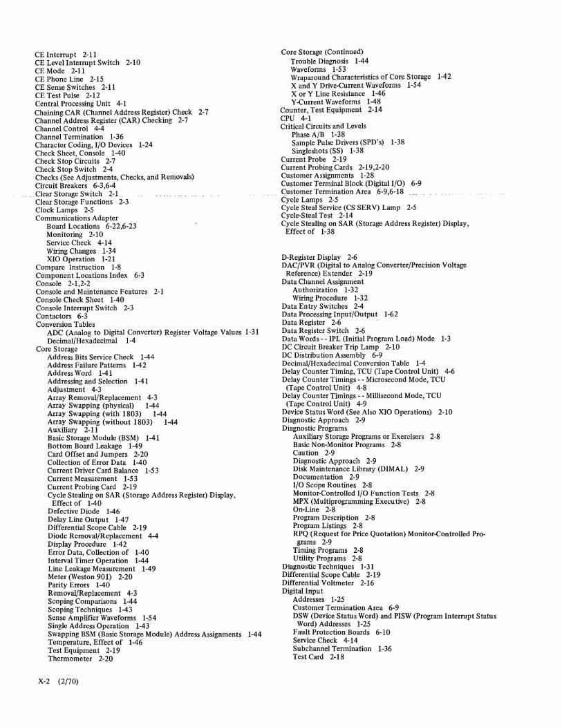
CE Interrupt 2-11 CE Level Interrupt Switch 2-10 CEMode 2-11 CE Phone Line 2-15 CE Sense Switches 2-11 CE Test Pulse 2-12 Central Processing Unit 4-1 Chaining CAR (Channel Address Register) Check 2-7 Channel Address Register (CAR) Checking 2-7 Channel Control 4-4 Channel Tennination 1-36 Character Coding, I/O Devices 1-24 Check Sheet, Console 1-40 Check Stop Circuits 2-7 Check Stop Switch 2-4 Checks (See Adjustments, Checks, and Removals) Circuit Breakers 6-3,6-4
_ Clear Storage Switch 2-L Clear Storage Functions 2-3 Clock Lamps 2-5 Communications Adapter
Board Locations 6-22,6-23 Monitoring 2-10 Service Check 4-14 Wiring Changes 1-34 XIO Operation 1-21
Compare Instruction 1-8 Component Locations Index 6-3 Console 2-1,2-2 Console and Maintenance Features 2-1 Console Check Sheet 1-40 Console Interrupt Switch 2-3 Contactors 6-3 Conversion Tables
ADC (Analog to Digital Converter) Register Voltage Values 1-31 Decimal/Hexadecimal 1-4
Core Storage Address Bits Service Check 1-44 Address Failure Patterns 1-42 Address Word 1-41 Addressing and Selection 1-41 Adjustment 4-3 Array Removal/Replacement 4-3 Array Swapping (physical) 1-44 Array Swapping (with 1803) 1-44 Array Swapping (without 1803) 1-44 Auxiliary 2-11 Basic Storage Module (BSM) 1-41 Bottom Board Leakage 1-49 Card Offset and Jumpers 2-20 Collection of Error Data 1-40 Current Driver Card Balance 1-53 Current Measurement 1-53 Current Probing Card 2-19 Cycle Stealing on SAR (Storage Address Register) Display,
Effect of 1-40 Defective Diode 1-46 Delay Line Output 1-47 Differential Scope Cable 2-19 Diode Removal/Replacement 4-4 Display Procedure 1-42 Error Data, Collection of 1-40 Interval Timer Operation 1-44 Line Leakage Measurement 1-49 Meter (Weston 901) 2-20 Parity Errors 1-40 Removal/Replacement 4-3 Scoping Comparisons 1-44 Scoping Techniques 1-43 Sense Amplifier Waveforms 1-54 Single Address Operation 1-43 Swapping BSM (Basic Storage Module) Address Assignments 1-44 Temperature, Effect of 1-46 Test Equipment 2-19 Thermometer 2-20
X-2 (2/70)
Core Storage (Continued) Trouble Diagnosis 1-44 Waveforms 1-53 Wraparound Characteristics of Core Storage 1-42 X and Y Drive-Current Wavefonns 1-54 X or Y Line Resistance 1-46 Y -Current Waveforms 1-48
Counter, Test Equipment 2-14 CPU 4-1 Critical Circuits and Levels
Phase A/B 1-38 Sample Pulse Drivers (SPD's) 1-38 Singleshots (SS) 1-38
Current Probe 2-19 Current Probing Cards 2-19,2-20 Customer Assignments 1-28 Customer Terminal Block (Digital I/O) 6-9 <:!lstomer Tennination Area _6-9,6-18 ___ _ Cycle Lamps 2-5 Cycle Steal Service (CS SERV) Lamp 2-5 Cycle-S teal Test 2-14 Cycle Stealing on SAR (Storage Address Register) Display,
Effect of 1-38
D-Register Display 2-6 DAC/PVR (Digital to Analog Converter/Precision Voltage
Reference) Extender 2-19 Data Channel Assignment
Authorization 1-32 Wiring Procedure 1-32
Data Entry Switches 2-4 Data Processing Input/Output 1-62 Data Register 2-6 Data Register Switch 2-6 Data Words - - IPL (Initial Program Load) Mode 1-3 DC Circuit Breaker Trip Lamp 2-10 DC Distribution Assembly 6-9 Decimal/Hexadecimal Conversion Table 1-4 Delay Counter Timing, TCU (Tape Control Unit) 4-6 Delay Counter Timings - - Microsecond Mode, TCU
(Tape Control Unit) 4-8 Delay Counter Timings - - Millisecond Mode, TCU
(Tape Control Unit) 4-9 Device Status Word (See Also XIO Operations) 2-10 Diagnostic Approach 2-9 Diagnostic Programs
Auxiliary Storage Programs or Exercisers 2-8 Basic Non-Monitor Programs 2-8 Caution 2-9 Diagnostic Approach 2-9 Disk Maintenance Library (DIMAL) 2-9 Documentation 2-9 I/O Scope Routines 2-8 Monitor-Controlled I/O Function Tests 2-8 MPX (Multiprogramming Executive) 2-8 On-Line 2-8 Program Description 2-8 Program Listings 2-8 RPQ (Request for Price Quotation) Monitor-Controlled Programs 2-9
Timing Programs 2-8 Utility Programs 2-8
Diagnostic Techniques 1-31 Differential Scope Cable 2-19 Differential Voltmeter 2-16 Digital Input
Addresses 1-25 Customer Tennination Area 6-9 DSW (Device Status Word) and PISW (Program Interrupt Status
Word) Addresses 1-25 Fault Protection Boards 6-10 Service Check 4-14 Sub channel Termination 1-36 Test Card 2-18
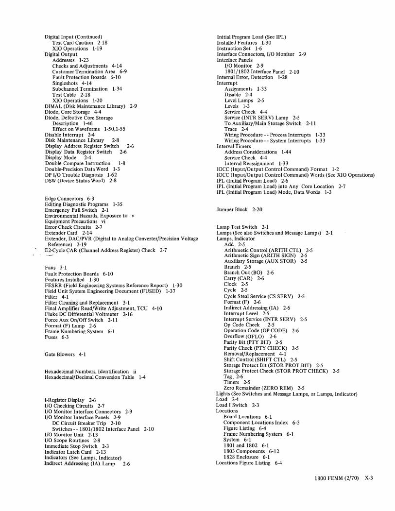
Digital Input (Continued) Test Card Caution 2-18 XIO Operations 1-19
Digital Output Addresses 1-23 Checks and Adjustments 4-14 Customer Termination Area 6-9 Fault Protection Boards 6-10 Singleshots 4-14 Subchannel Termination 1-34 Test Cable 2-18 XIO Operations 1-20
DIMAL (Disk Maintenance Library) 2-9 Diode, Core Storage 4-4 Diode, Defective Core Storage
Description 1-46 Effect on Waveforms 1-50,1-55
Disable Interrupt 2-4 Disk Maintenance Library 2-8 Display Address Register Switch 2-6 Display Data Register Switch 2-6 Display Mode 2-4 Double Com'pare Instruction 1-8 Double-Precision Data Word 1-3 DP I/O Trouble Diagnosis 1-62 DSW (Device Status Word) 2-8
Edge Connectors 6-3 Editing Diagnostic Programs 1-35 Emergency Pull Switch 2-1 Environmental Hazards, Exposure to v Equipment Precautions vi Error Check Circuits 2-7 Extender Card 2-14 Extender, DAC/PVR (Digital to Analog Converter/Precision Voltage
Reference) 2-19 E2-Cycle CAR (Channel Address Register) Check 2-7
Fans 3-1 Fault Protection Boards 6-10 Features Installed 1-30 FESRR (Field Engineering Systems Reference Report) 1-30 Field Unit System Engineering Document (FUSED) 1-37 Filter 4-1 Filter Cleaning and Replacement 3-1 Final Amplifier Read/Write Adjustment, TCU 4-10 Fluke DC Differential Voltmeter 2-16 Force Aux On/Off Switch 2-11 Format (F) Lamp 2·6 Frame Numbering System 6-1 Fuses 6-3
Gate Blowers 4-1
Hexadecimal Numbers, Identification ii Hexadecimal/Decimal Conversion Table 1-4
I-Register Display 2-6 I/O Checking Circuits 2-7 I/O Monitor Interface Connectors 2-9 I/O Monitor Interface Panels 2-9
DC Circuit Breaker Trip 2-10 Switches - - 1801/1802 Interface Panel 2-10
I/O Monitor Unit 2-13 I/O Scope Routines 2-8 Immediate Stop Switch 2-3 Indicator Latch Card 2-13 Indicators (See Lamps, Indicator) Indirect Addressing (lA) Lamp 2-6
Initial Program Load (See IPL) Installed Features 1-30 Instruction Set 1-6 Interface Connectors, I/O Monitor 2-9 Interface Panels
I/O Monitor 2-9 1801/1802 Interface Panel 2-10
Internal Error, Detection 1-28 Interrupt
Assignments 1-33 Disable 2-4 Level Lamps 2-5 Levels 1-3 Service Check 4-4 Service (INTR SERV) Lamp 2-5 To Auxiliary/Main Storage Switch 2-11 Trace 2-4 Wiring Procedure - - Process Interrupts 1-33 Wiring Procedure - - System Interrupts 1-33
Interval Timers Address Considerations 1-44 Service Check 4-4 Interval Reassignment 1-33
IOCC (Input/Output Control Command) Format 1-2 IOCC (Input/Output Control Command) Words (See XIO Operations) IPL (Initial Program Load) 2-6 IPL (Initial Program Load) into Any Core Location 2-7 IPL (Initial Program Load) Mode, Data Words 1-3
Jumper Block 2-20
Lamp Test Switch 2-1 Lamps (See also Switches and Message Lamps) 2-1 Lamps, Indicator
Add 2-5 Arithmetic Control (ARITH CTL) 2-5 Arithmetic Sign (ARITH SIGN) 2-5 Auxiliary Storage (AUX STOR) 2-5 Branch 2-5 Branch Out (BO) 2-6 Carry (CAR) 2-6 Clock 2-5 Cycle 2-5 Cycle Steal Service (CS SERV) 2-5 Format (F) 2-6 Indirect Addressing (IA) 2-6 Interrupt Level 2-5 . Interrupt Service (INTR SERV) 2-5 Op Code Check 2-5 Operation Code (OP CODE) 2-6 Overflow (OFLO) 2-6 Parity Bit (PTY BIT) 2-5 Parity Check (PTY CHECK) 2-5 Removal/Replacement 4-1 Shift Control (SHIFT CTL) 2-5 Storage Protect Bit (STOR PROT BIT) 2-5 Storage Protect Check (STOR PROT CHECK) 2-5 Tag, 2-6 Timers 2-5 Zero Remainder (ZERO REM) 2-5
Lights (See Switches and Message Lamps, or Lamps, Indicator) Load 2-4 Load I Switch 2-3 Locations
Board Locations 6-1 Component Locations Index 6-3 Figure Listing 6-4 Frame Numbering System 6-1 System 6-1 1801 and 1802 6-1 1803 Components 6-12 1828 Enclosure 6-1
Locations Figure Listing 6-4
1800 FEMM (2/70) X-3
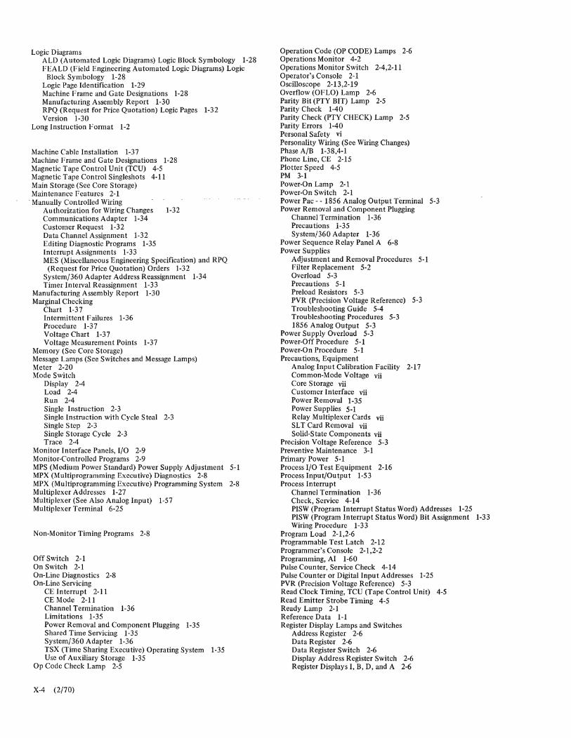
Logic Diagrams ALD (Automated Logic Diagrams) Logic Block Symbology 1-28 FEALD (Field Engineering Automated Logic Diagrams) Logic
Block Symbology 1-28 Logic Page Identification 1-29 Machine Frame and Gate Designations 1-28 Manufacturing Assembly Report 1-30 RPQ (Requcst for Price Quotation) Logic Pages 1-32 Version 1-30
Long Instruction Format 1-2
Machine Cable Installation 1-37 Machine Frame and Gate Designations 1-28 Magnetic Tape Control Unit (TCU) 4-5 Magnetic Tape Control Singleshots 4-11 Main Storage (See Core Storage) Maintenance Features 2-1
. Manually Controlled Wiring Authorization for Wiring Changes 1-32 Communications Adapter 1-34 Customer Request 1-32 Data Channel Assignment 1-32 Editing Diagnostic Programs 1-35 Interrupt Assignments 1-33 MES (Miscellaneous Engineering Specification) and RPQ
(Request for Price Quotation) Orders 1-32 System/360 Adapter Address Reassignment 1-34 Timer Interval Reassignment 1-33
Manufacturing Assembly Report 1-30 Marginal Checking
Chart 1-37 In termi ttcn t Failures 1-36 Procedure 1-37 Voltage Chart 1-37 Voltage Measurement Points 1-37
Memory (See Core Storage) Message Lamps (See Switches and Message Lamps) Meter 2-20 Mode Switch
Display 2-4 Load 2-4 Run 2"4 Single Instruction 2-3 Single Instruction with Cycle Steal 2-3 Single Step 2-3 Single Storage Cycle 2-3 Trace 2-4
Monitor Interface Panels, I/O 2-9 Monitor-Controlled Programs 2-9 MPS (Medium Power Standard) Power Supply Adjustment 5-1 MPX (Multiprogramming Executive) Diagnostics 2-8 MPX (Multiprogramming Executive) Programming System 2-8 Multiplexer Addresses 1-27 Multiplexer (See Also Analog Input) 1-57 Multiplexer Terminal 6-25
Non-Monitor Timing Programs 2-8
Off Switch 2-1 On Switch 2-1 On-Line Diagnostics 2-8 On-Line Servicing
CE Interrupt 2-11 CE Mode 2-11 Channel Termination 1-36 Limitations 1-35 Power Removal and Component Plugging 1-35 Shared Time Servicing 1-35 System/360 Adapter 1-36 TSX (Time Sharing Executive) Operating System 1-35 Use of Auxiliary Storage 1-35
Op Code Check Lamp 2-5
X-4 (2/70)
Operation Code (OP CODE) Lamps 2-6 Operations Monitor 4-2 Operations Monitor Switch 2-4,2-11 Operator's Console 2-1 Oscilloscope 2-13,2-19 Overflow (OFLO) Lamp 2-6 Parity Bit (PTY BIT) Lamp 2-5 Parity Check 1-40 Parity Check (PTY CHECK) Lamp 2-5 Parity Errors 1-40 Personal Safety vi Personality Wiring (See Wiring Changes) Phase A/B 1-38,4-1 Phonc Line, CE 2-15 Plotter Speed 4-5 PM 3-1 Power-On Lamp 2-1 Power-On Switch 2-1 Power Pac - - 1856 Analog Output Terminal 5-3 Power Removal and Component Plugging
Channel Termination 1-36 Precautions i-35 System/360 Adapter 1-36
Power Sequence Relay Panel A 6-8 Power Supplies
Adjustment and Removal Procedures 5-1 Filter Replacement 5-2 Overload 5-3 Precau tions 5-1 Preload Resistors 5-3 PVR (Precision Voltage Reference) 5-3 Troubleshooting Guide 5-4 Troubleshooting Procedures 5-3 1856 Analog Output 5-3
Power Supply Overload 5-3 Power-Off Procedure 5-1 Power-On Procedure 5-1 Precautions, Equipment
Analog Input Calibration Facility 2-17 Common-Mode Voltage vii Core Storage vii Customer Interface vii Power Removal 1-35 Power Supplies 5-1 Relay Multiplexer Cards vii SLT Card Removal vii Solid-State Components vii
Precision Voltage Reference 5-3 Preventive Maintenance 3-1 Primary Power 5-1 Process I/O Test Equipment 2-16 Process Input/Output 1-53 Process Interrupt
Channel Termination 1-36 Check, Service 4-14 PISW (Program Interrupt Status Word) Addresses 1-25 PISW (Program Interrupt Status Word) Bit Assignment 1-33 Wiring Procedure 1-33
Program Load 2-1,2-6 Programmable Test Latch 2-12 Programmer's Console 2-1,2-2 Programming, AI 1-60 Pulse Counter, Service Check 4-14 Pulse Counter or Digital Input Addresses 1-25 PVR (Precision Voltage Reference) 5-3 Read Clock Timing, TCU (Tape Control Unit) 4-5 Read Emitter Strobe Timing 4-5 Ready Lamp 2-1 Reference Data 1-1 Register Display Lamps and Switches
Address Register 2-6 Data Register 2-6 Data Register Switch 2-6 Display Address Register Switch 2-6 Register Displays I, B, D, and A 2-6
Relays 6-3 Remote Switch Box 2-15 Removals (See Adjustments, Checks, and Removals) Repeatability, Analog Input 1-61 Reserved Main Storage Locations 1-3 Reset Switch 2-3 Resistance Bulb Thermometer 4-12 RPQ (Request for Price Quotation) Logic Pages 1-28 RPQ (Request for Price Quotation) Monitor-Controlled Programs 2-9 Run Lamp 2-1 Run Switch 2-4
Safety Exposure to Environmental Hazards vi Line-Powered Equipment vii Machine Warning Labels vii Oscilloscopes vii Personal vi Power Cords vii
. Power Supplies vii Sample Pulse Drivers (SPD's) 1-38 Selector Channel
Board Locations 6-22,6-23 Monitoring 2-10 Service Check 4-14 Singleshot Adjustment 4-14 XIO Operation 1-22
Sense and Program Switches 2-4 Serpent Connector Contacts 1-37 Service Checks (See Adjustments, Checks, and Removals) Servicing Limitations
Channel Termination 1-36 Power Removal and Component Plugging 1-37 Shared Time Servicing 1-35 System/360 Adapter 1-36 TSX (Time Sharing Executive) Operating System 1-36 Use of Auxiliary Storage 1-35
r- __ ShifLControl (SHIFT CTL) Lamp 2-5 Short Instructitm Format 1-1 Signal Acceptance and Rejection Levels, TCU 4-7 Signal Cables 1-37 Single Instruction 2-3 Single Instruction with Cycle Steal 2-3 Single Step 2-3 Single Storage Cycle 2-3 Singleshot Triggering 1-38 Single-Precision Data Word 1-2 SLT Contact Wear 1-37 SLT Maintenance
Field Unit System Engineering Document (FUSED) 1-37 Machine Cable Installation 1-37 SLT Contact Wear 1-37 Voltage Levels and Delays 1-37 Wire Color Codes 1-37
Sound-Powered Phones 2-15 SPD's (Sample Pulse Drivers) 1-38 Special Circuits A-I Special Purpose Wiring 1-30 Start Switch 2-3 Stop Immediate Switch 2-3 Storage Protect Bit (STOR PROT BIT) Lamp 2-5 Storage Protect Check (STOR PROT CHECK) Lamp 2-5 Storage (See Core Storage) Storage-Protect Bit 2-5 Switch Box (Remote) 2-15 Switches and Message Lamps
Alarm Lamp 2-1 Clear Storage 2-1 Console-Interrupt Switch 2-3 Emergency Pull 2-1 Immediate Stop 2-3 Indicator Lamps 2-4 Lamp Test 2-1 Load I Switch 2-3
Switches and Message Lamps (Continued) Mode 2-3 Off 2-1 On 2-1 PowerOn 2-1 Program Load 2-1 Ready 2-1 Register Display Lamps and Switches 2-6 Removal/Replacement 4-1 Reset 2-3 Run 2-4 Start 2-3 Stop 2-3 Toggle Switches 2-4 Wait 2-1
Switches - - 1801/1802 Interface Panel 2-10 CE Level Interrupt 2-10 CE Sense 2-10 Force Auxiliary On/Off 2-10 Interrupt to Auxiliary/Main Storage 2-10 Operations Monitor 2-11 Use Meter 2-10
Switches, Toggle 2-4 System Paperwork Binder 1-30 System Power-Off Procedure 5-1 System Power-On Procedure 5-1 System/360 Adapter
Address Reassignment 1-34 Adjustment and Service Check 4-11 Disconnecting 1800 System 1-35 Monitoring 2-10 Service Check 4-1 To Power Down 1-35 To Power Up 1-35 Wiring Procedure 1-34
T -Clock Lamps 2-5 Tag Lamps 2-6 Tape Control Unit 4-5 TCU 4-5 Temperature Tracking 4-3 Terminal Boards 6-3 Test Cable 2-18 Test Equipment
Core Storage 2-19 General 2-13 List of Test Equipment A-I Process I/O 2-16 Seven Position Counter 2-14
Thermometer 2-20 Time Intervals, Op Monitor 2-11 Time Pulses A, Band C 1-29 Timer Interval Reassignment
Authorization 1-33 Wiring Procedure 1-33
Timer Lamps 2-5 Toggle Switches
Check Stop 2-4 Data Entry 2-4 Disable interrupt 2-4 Operations Monitor 2-4 Sense and Program 2-4 Write Storage Protect Bits 2-4
Tools and Test Equipment 2-13,A-l Trace 2-4 Triggering Singleshots 1-38 Troubleshooting Procedures, Power Supplies 5-3
Use Meter Switch 2-10 Utility Programs 2-8
Vector Addresses, Interrupt 1-3 Voltage Crossover Assemblies 1-37
1800 FEMM (2/70) X-5
Voltage, Primary 5-1 Voltages
1801/1802 5-5 1826 Data Adapter Unit 5-6 1856 Analog Output 5-7 2310 Disk Storage 5-6
Wait Lamp 2-1 Wire Color Codes 1-37 Wired Logic (WL) Jumpering
Interrupt, Cycle-Steal, IPL 6-3 Other 6-3
Wiring Changes, Manually Controlled Authorization for Wiring Changes 1-32 Customer Request 1-32 Communications Adapter 1-34 Data Channel Assignment 1-32 Description - 1-30 - -Editing Diagnostic Programs 1-35 Interrupt Assignments 1-33 Line Adapters 1-34 MES (Miscellaneous Engineering Specification) and RPQ
(Request for Price Quotation) Orders 1-32 System/360 Adapter Address Reassignment 1-34 Timer Interval Reassignment 1-33
World Trade A-I Wraparound Characteristics of Core Storage 1-42 Write Clock Timing, TCU (Tape Control Unit) 4-6 Write Storage Protect Bits Switch 2-4
X or Y Line Resistance, Core Storage 1-46 X-Clock Lamps 2-5 XIO Operations
Analog Input 1-17 Communications Adapter 1-21 Digital and Analog Output 1-20 Digital Input 1-19 Internal (Area Zero) 1-9 Selector Channel 1-22 System/360 Adapter 1-17 Tape Control Unit 1-15 1053 Printer and 1816 Printer-Kcyboard 1-10 1054 Paper Tape Reader and 1055 Paper Tape Punch 1-11 1442 Card Read Punch 1-12 1443 Printer 1-13 1627 Plotter 1-13 1810 Disk Storage 1-14
Zero Remainder (ZERO REM) Lamp 2-5
1053 (See 1816) 1054-1055 Paper Tape
Adapter Locations 6-10,6-11 Adapter Service Check 4-4 Adjustments 4-4 DC Voltages 5-5 IPL (Initial Program Load) Data Word 1-3 IPL (Initial Program Load) Procedure 2-7 XIO Operations 1-11
X-6 (2/70)
1442 Card Read Punch Adapter Location 6-10,6-11 Character Coding 1-24 Checks and Adjustment 4-5 DC Voltages 5-5 IPL (Initial Program Load) Data Word 1-3 IPL (Initial Program Load) Procedure 2-6 Power Down Procedure 1-62 XIO Operations 1-12
1443 Printer Adapter Location 6-10,6-11 Carriage Control Chars. 1-25 Character Coding 1-24 Service Check 4-5 XIO Operations 1-13
1627 Plotter Adapter Location 6-10,6-11
_ S!lrvic!l Check _ 4-5 Speed Change 4-5 XIO Operations 1-13
1800 System Console Check Sheet 1-40
1801, 1802 Processor-Controllers Checks and Adjustments 4-1 Locations 6-1 through 6-11 PM 3-1 Power Supplies 5-5
1810 Disk Storage Service Check 4-5 Voltages 5-7
1803 Core Storage Unit Address Swapping 1-44 BSM (Basic Storage Module) Locations 6-15 Interval Timer Operation 1-44 Locations 6-12 Selection 1-41 Time Pulses A, B, and C 1-29 Wraparound 1-42
1816-1053 Printers Character Coding 1-24 Checks and Adjustments 4-4 DC Voltages 5-5 XIO Operations 1-10
1826 Data Adapter Channel Termination 1-36 Locations 6-1 through 6-23 PM 3-1 Power Supplies 5-6,5-7
1828 Enclosure Locations 6-1 through 6-24
1851 Multiplexer Terminal (See Also Analog Input) Locations 6-1 through 6-25
1856 Analog Output Terminal Channel Termination 1-36 Blower Filter Replacement 4-13 Blower Removal 4-12 DAC/PVR (Digital to Analog Converter/Precision Voltage
Reference) Extender 2-19 Locations 6-1 through 6-26 PM 3-1 Power Pac 5-3 Precision Voltage Reference 5-3
2401-2402 Magnetic Tape Adapter Location 6-11 Checks and Adjustments 4-5 XIO Operations 1-15
Copyright © 2022 FDOKUMEN