Ceramic Micro Heater Technology for Gas Sensors
10
ROMANIAN JOURNAL OF INFORMATION SCIENCE AND TECHNOLOGY Volume 10, Number 1, 2007, 43–52 Ceramic Micro Heater Technology for Gas Sensors C. MOLDOVAN 1 , O. NEDELCU 1 , P. JOHANDER 2 , I. GOENAGA 3 , D. GOMEZ 3 , P. PETKOV 4 , U. KAUFMANN 5 , H.-J. RITZHAUPT-KLEISSL 5 , R. DOREY 6 , K. PERSSON 7 1 National Institute for R&D in Microtechnologies, Erou Iancu Nicolae 32 B, Bucharest 077190, Romania 2 IVF – Industrial Research and Development Corporation; Argongatan 30, S431 53 Molndal, Sweden 3 Fundacion Tekniker, Micro and Nanotechnology Department, Av. Otaola 20, 20600 Eibar, Spain 4 Manufacturing Engineering and Multidisciplinary Technology Centre, Cardiff University, UK 5 Forschungszentrum Karlsruhe, Institut f¨ ur Materialforschung III, P.O. Box 3640, 76021 Karlsruhe, Germany 6 Nanotechnology Group, Cranfield University, Cranfield, Bedfordshire, UK 7 IMEGO, Arvid Hedvalls Backe 4, SE 411 33 Goteborg, Sweden Abstract. The paper presents the design and manufacturing steps of mi- cro heaters, built on ceramic suspended membranes for gas sensor applications. The micro heaters are designed and fabricated by combining laser milling tech- niques, and conductive ceramic technology. Trenches are created in the ceramic substrate in order to define the geometry of the heater using laser processing of the substrate. The heater is completed by filling the trenches with conduc- tive ceramic paste and then baking to remove the solvent from the paste. The final step involves releasing the membrane by laser milling, enabling it to be suspended on four bridges, to minimise the dissipation of the heat in the sub- strate. The temperature of the heater element was measured with a heat camera from FLIR 40 system comparing the case of the heater positioned on top of a released membrane and that of the non-released membrane. The simulation of the heater build on top of a released membrane was compared with the heater measurements. Keywords: Micro heaters, gas sensor.
-
Upload
independent -
Category
Documents
-
view
0 -
download
0
Transcript of Ceramic Micro Heater Technology for Gas Sensors

ROMANIAN JOURNAL OF INFORMATIONSCIENCE AND TECHNOLOGYVolume 10, Number 1, 2007, 43–52
Ceramic Micro Heater Technologyfor Gas Sensors
C. MOLDOVAN1, O. NEDELCU1, P. JOHANDER2,
I. GOENAGA3, D. GOMEZ3, P. PETKOV4, U. KAUFMANN5,H.-J. RITZHAUPT-KLEISSL5, R. DOREY6, K. PERSSON7
1National Institute for R&D in Microtechnologies,Erou Iancu Nicolae 32 B, Bucharest 077190, Romania
2IVF – Industrial Research and Development Corporation;Argongatan 30, S431 53 Molndal, Sweden
3Fundacion Tekniker, Micro and Nanotechnology Department,Av. Otaola 20, 20600 Eibar, Spain
4Manufacturing Engineering and Multidisciplinary Technology Centre,Cardiff University, UK
5Forschungszentrum Karlsruhe, Institut fur Materialforschung III,P.O. Box 3640, 76021 Karlsruhe, Germany
6Nanotechnology Group, Cranfield University,Cranfield, Bedfordshire, UK
7IMEGO, Arvid Hedvalls Backe 4, SE 411 33 Goteborg, Sweden
Abstract. The paper presents the design and manufacturing steps of mi-
cro heaters, built on ceramic suspended membranes for gas sensor applications.
The micro heaters are designed and fabricated by combining laser milling tech-
niques, and conductive ceramic technology. Trenches are created in the ceramic
substrate in order to define the geometry of the heater using laser processing
of the substrate. The heater is completed by filling the trenches with conduc-
tive ceramic paste and then baking to remove the solvent from the paste. The
final step involves releasing the membrane by laser milling, enabling it to be
suspended on four bridges, to minimise the dissipation of the heat in the sub-
strate. The temperature of the heater element was measured with a heat camera
from FLIR 40 system comparing the case of the heater positioned on top of a
released membrane and that of the non-released membrane. The simulation of
the heater build on top of a released membrane was compared with the heater
measurements.
Keywords: Micro heaters, gas sensor.

44 C. Moldovan et al.
1. Introduction
Micro heaters are an essential part in chemoresistive gas sensors [1]. The heatingelement must create an accurate and uniform heating of the sensor surface. The hea-ting element is normally made on Silicon, LTCC or alumina substrate. The commonmethods to manufacture heating element is thin film deposition of metal and litho-graphic/ etch process [2] and thick film screen printed on LTCC and alumina [3]. Theheat distribution in such 2D design concepts is not so good due to the spreading ofheat and thus quite large power consumption. This could be improved by a 3D designconcept by suspending the heating element in four bridges, so the heating and sen-sing element will be thermally isolated from the surrounding substrate. This has beendemonstrated in silicon by bulk etching of silicon [4], [5]. This design gives a muchmore uniform heating of the sensor surface and much faster heating characteristics.In this paper we demonstrate a similar design concept by laser machining in LTCCand alumina.
Laser milling process overview
Laser milling involves applying laser energy to remove material through ablationin a layer-by-layer fashion. CNC programs for laser milling are obtained directly froma three-dimensional CAD model of the workpiece. Thus, apart from being a materialremoval rather than material accretion system, a laser-milling machine operates likeany other layered technology manufacturing equipment.
Material removal
The laser milling process removes material as a result of interaction between thelaser beam and the substrate or workpiece. Several removal mechanisms can takeplace, depending on a number of process parameters related to the beam and theworkpiece material.
During interaction between the laser radiation and the material, electrons in thesubstrate are excited by the laser photons. As a result, the electron subsystem isheated to a high temperature and the absorbed energy is transferred to the atomiclattice [6]. Energy losses are caused by heat transport via electrons into the bulk ofthe substrate. According to classical linear theory, light absorption is described bythe Beer-Lambert law, which states that the absorption of a particular wavelength oflight transmitted through a material is a function of the material path length and isindependent of the incident intensity. For the very high intensities, which can be achie-ved in laser processing, non-linear phenomena take place and cause stronger energyabsorption. According to the linear absorption model, the electrons excited by photonabsorption transfer the heat energy to the lattice and cause melting or vaporisation.In the case of extreme intensities, as with ultrashort pulse ablation, the bound elec-trons of the material can be directly freed. Effects such as multiphoton absorptionand avalanche ionisation can be observed. Thermal conduction in the material drawsenergy away from the focal spot and leads to heat affected zones. For metals, laser

Ceramic Micro Heater Technology for Gas Sensors 45
light absorption is not a major problem, because the band structure of the materialallows the absorption of most low-to-moderate energy photons. Metals absorb laserradiation with their electrons in the conduction band and near to the Fermi level. Forsemiconductors and insulators, including ceramics and polymers, the Fermi level isbetween the valence and conduction bands. The requirement that an electron has toabsorb enough energy to pass through the forbidden region between the valence andconduction bands sets a limit on the photon energies that can be absorbed by a linearprocess. There are two methods for non-linear absorption: an electron avalanche anda strong multiphoton absorption.
In the case of an electron avalanche, some electrons with intermediate energies areexcited into the conduction band by single photon absorption. The electrons in theconduction band can absorb single photons of the incident light, which will increasetheir energy. These electrons collide with bound electrons, which lead to avalancheionisation.
Multiphoton absorption is another mechanism for non-linear absorption in whichan electron transfers from the valence band to the conduction band by absorbingseveral photons. In general, as materials reach a critical density of electrons, theystart to absorb sufficient photon energy to undergo ablation. It is important to notethat there is a material dependent ablation threshold fluence, below which the laserablation cannot start and material removal is not feasible.
The response of the substrate to laser radiation is influenced by a number ofmaterial characteristics. Hence, for optimal machining results a proper match of lasersource and material should be achieved. Generally, higher absorption efficiency leadsto a more effective laser milling process. Thermal conductivity is another key materialfactor. This affects the dissipation of the absorbed energy into the bulk of the material,the energy losses, the material removal efficiency and the dimensions of the heataffected zone (HAZ) [7], [8].
2. Experimental set up
A commercial femtosecond Ti:sapphire laser system has been used to perform themicromachining of LTCC and briefly, the system is basically composed by:
(i) a femtosecond seed laser (Coherent, Vitesse LP SB) with an output averagepower of 250 mW at a pulse repetition rate (PRR) of 80 MHz;
(ii) a multipass amplifier (Quantronix, Odin-Compact DP 1.0) based on ChirpedPulse Amplification (CPA);
(iii) a LBO crystal for doubling the natural wavelength of Ti: sapphire beam fromλ = 800 nm to λ = 400 nm by means of Second Harmonic Generation (SHG)techniques.
The resulting beam, used to perform all the experimental tests presented in thiswork, is gaussian (beam quality, M2 ∼1.2 (TEM00)), circular (3 mm in diameter),ultraviolet (λ = 400 nm), pulse length is 90 fs and the maximum energy peak is

46 C. Moldovan et al.
350 µJ. Fluence on the sample has been controlled by the rotation of a half-wave platethat changes the polarization plane of the beam before the LBO crystal. Consideringthat the conversion efficiency strongly depends on the polarization direction, it waspossible to control energy variations from 0 µJ to 350 µJ in steps of 1 µJ.
The samples for the experimental tests were placed in a computer controlled XYZ-stage positioning system from Aerotech with resolution of 0.1 µm and repeatability(3σ) of 1 µm in the case of the XY-stages and 0.5 µm and 2 µm, respectively, forthe Z-stage. A circular 2 mm mask was used before focusing the beam on the samplein order to remove the tails of the gaussian profile. A fused silica plano-convex lenswith focal length of 100 mm (Newport, SPX022) was used as focusing optics. In allcases, focal point was focused on the surface of the sample and no image projectiontechnique was used.
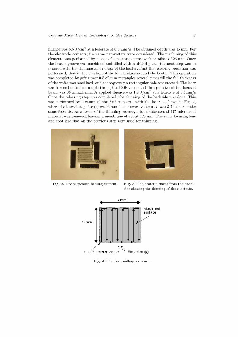
3. Design and manufacturing
The heating element is suspended in four supporting bridges that also serve aselectrical leads to the heating elements (see Fig. 1). The two other beams could beused for connection of sensor element. The heating element is a serpentine directlylaser-milled into the substrate material and filled with AuPtPd paste. The heaterelement is released by laser milling and the backside of the heater is thinned so thethermal mass is reduced (Figs. 2 and 3).
Fig. 1. The design of the electroceramic heater(100 mm width) on the ceramic membrane (2 000×2 000 mm2)
suspended on four bridges (300×200 mm2 each).
Laser technology has been performed for:
(i) the micromachining of a groove-electrode structure where conductive ceramicpaste will be embedded;
(ii) the thin and release of the microheater, driving to a suspended membrane.
In the first case, the laser was slightly de-focussed on the sample in order to get abigger spot size, leading to a faster machining of the 100 mm-wide grooves. The applied
Ceramic Micro Heater Technology for Gas Sensors 47
fluence was 5.5 J/cm2 at a federate of 0.5 mm/s. The obtained depth was 45 mm. Forthe electrode contacts, the same parameters were considered. The machining of thiselements was performed by means of concentric curves with an offset of 25 mm. Oncethe heater groove was machined and filled with AuPtPd paste, the next step was toproceed with the thinning and release of the heater. First the releasing operation wasperformed, that is, the creation of the four bridges around the heater. This operationwas completed by going over 0.5×2 mm rectangles several times till the full thicknessof the wafer was machined, and consequently a rectangular hole was created. The laserwas focused onto the sample through a 100FL lens and the spot size of the focusedbeam was 36 mm±1 mm. A applied fluence was 1.8 J/cm2 at a federate of 0.5mm/sOnce the releasing step was completed, the thinning of the backside was done. Thiswas performed by “scanning” the 3×3 mm area with the laser as shown in Fig. 4,where the lateral step size (s) was 6 mm. The fluence value used was 3.7 J/cm2 at thesame federate. As a result of the thinning process, a total thickness of 175 microns ofmaterial was removed, leaving a membrane of about 225 mm. The same focusing lensand spot size that on the previous step were used for thinning.
Fig. 2. The suspended heating element. Fig. 3. The heater element from the back-
side showing the thinning of the substrate.
Fig. 4. The laser milling sequence.

48 C. Moldovan et al.
4. Measurement of the thermal properties
The temperature of the heater element was measured with a heat camera fromFLIR 40 system. This system could record 50 images/s and the dynamics of thesystem could be analysed. The heater reaches about 490◦C in 5 seconds.
Fig. 5. The power-on curve for the released
heater element.
Fig. 6. The heat distribution from the released
heating element.
Fig. 7. The Non-released heater element.
Ceramic Micro Heater Technology for Gas Sensors 49
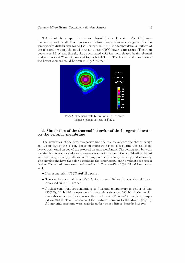
This should be compared with non-released heater element in Fig. 8. Becausethe heat spread in all directions outwards from heater elements we get at circulartemperature distribution round the element. In Fig. 6 the temperature is uniform atthe released area and the outside area at least 400◦C lower temperature. The inputpower was 1.1 W and this should be compared with the non-released heater elementthat requires 2.4 W input power of to reach 490◦C [1]. The heat distribution aroundthe heater element could be seen in Fig. 8 below.
Fig. 8. The heat distribution of a non-released
heater element as seen in Fig. 7.
5. Simulation of the thermal behavior of the integrated heateron the ceramic membrane
The simulation of the heat dissipation had the role to validate the chosen designand technology of the sensor. The simulations were made considering the case of theheater positioned on top of the released ceramic membrane. The comparison betweenthe simulation results and measurements results in the conditions of identical layoutand technological steps, allows concluding on the heaters processing and efficiency.The simulations have the role to minimize the experiments and to validate the sensordesign. The simulations were performed with CoventorWare2004, MemMech modu-le [1].
• Heater material: LTCC AuPdPt paste.
• The simulation conditions: 550◦C, Step time: 0.02 sec; Solver step: 0.01 sec;Analyzed time: 0 – 0.2 sec.
• Applied conditions for simulation: a) Constant temperature in heater volume(550◦C); b) Initial temperature in ceramic substrate: 293 K; c) Convectionthrough external surfaces: convection coefficient: 25 W/m2K; ambient tempe-rature: 293 K. The dimensions of the heater are similar to the Mask 1 (Fig. 1).All material constants were considered for the conditions described above.

50 C. Moldovan et al.
The results are presented in Figs. 9 and 10 indicating the thermal distribution inthe ceramic substrate after 0.02 s (Fig. 9) and after 0.2 s (Fig. 10). A very uniformdistribution of the heat after 0.2 s can be observed.
Fig. 9. Thermal distribution after 0.02 s at 550◦C.
Fig. 10. Thermal distribution after 0.2 s at 550◦C.
Figure 11 is describing the evolution of the heating process.

Ceramic Micro Heater Technology for Gas Sensors 51
Fig. 11. Evolution of average and minimum temperature
in alumina substrate.
Comparing Fig. 10 showing the simulation of the thermal distribution with Fig.6 showing the measurements of the heat distribution from the released heating ele-ment, we can conclude on the similarities of the thermal behaviour in terms of re-ached temperature (500◦C) and area of temperature distribution (identical for bothcases, concentrated on the released membrane). The membrane suspended by fourmicrobridges is uniformly heated at 500◦C, providing the needed temperature forthe working sensor. In the case of measurements, the time for uniformly heating ofthe membrane depends on the power supply. In the case of simulation, there are noelectrical parameters involved in the model, and the model is considering that thesubstrate will be kept at constant temperature 550◦C. That way, the differences ap-peared between simulation and measurements (Figs. 5 and 11) in terms of the timefor uniform heating of the substrate at 500◦C can be explained.
6. Conclusions
The purpose of the work was to establish the technology for obtaining heatersallowing the uniform heating of the sensor substrate to be used in gas sensors micro-fabrication.
The heaters design and manufacturing methodology described in the paper willact as a demonstrator for that technology. The main goal/overall objective is to obtainminiaturized, low cost devices on non-silicon substrates, with high sensitivity and lowpower consumption to be used in portable devices. The described technologies allowthe generation of new type of microsensors with existing tools (software, technologicalfacilities, etc.).
Acknowledgements. The authors express the acknowledgements to the 4M NoEfor supporting the work described in this paper. All results have been obtained in the

52 C. Moldovan et al.
frame of 4M, WP8 (Ceramic Cluster). Anders Lofgren Ericsson MicroWave for kindhelps with the IR measurements.
Literatur
[1] MOLDOVAN, C., NEDELCU, O., KAUFMANN, U., RITZHAUPT-KLEISSL, H.J.,DIMOV, S., PETKOV, P., DOREY, R., PERSSON, K., GOMEZ, D., JOHANDER,P., Proceedings 4M Conference on Multi Material Micro Manufacture, 29 June – 1 July2005, Karlsruhe, pp. 211–217.
[2] SHUEHL, J., CAVICCHI, R. E., GAITAN, M., SEMANCIK, S., IEEE Electron DevicesLett., 14, 1993, pp. 118–120.
[3] ZAWADA, T., DZIEDZIC, A., GOLONKA, L. J., 14th European Microelectronics andPackaging & Exhibition, Friedrichhafen, Germany, 23–25 June 2003.
[4] SEMANCIK, S., CAVICCHI, R. E., WHEELER, M. C., TIFFANY, J. E., POIRIER,G. E., WALTON, R. M., SUEHLE, J. S., PANCHAPAKESAN, B., DEVOE, D. L.,Sensor and Actuators, B77, 2001, pp. 579–591.
[5] WELCH, J., Micro-Machined Thin Film Hydrogen Gas Sensors, Proceedings 2002 USDOE Hydrogen Program Review NREL/CP-610-32405.
[6] SHIRK, M. D., MOLIAN, P. A., A review of ultrashort pulsed laser ablation of materials,Journal of Laser Applications, vol. 10, no. 1, 1998, pp. 18–28.
[7] KAUTEK, W., KRUGER, J., Femtosecond pulse laser ablation of metallic, semiconduc-ting, ceramic and biological materials, Proceedings SPIE, vol. 2207, 1994, pp. 600–610.
[8] VON DER LINDE, D., SOKOLOWSKI-TINTEN, K., The physical mechanisms ofshort-pulse laser ablation, Applied Surface Science, vol. 154–155, 2000, pp. 1–10.