Analysis on insulator–metal transition in yttrium doped LSMO from electron density distribution
Nano Res. 2010, 3(12): 874–880
874
Atomically Smooth Ultrathin Films of Topological Insulator Sb2Te3
Guang Wang1, Xiegang Zhu1, Jing Wen1, Xi Chen1, Ke He2, Lili Wang2, Xucun Ma2, Ying Liu3, 4, 5, Xi Dai2,
Zhong Fang2, Jinfeng Jia1, 4 ( ), and Qikun Xue1, 2 1 Key Lab for Atomic, Molecular and Nanoscience, Department of Physics, Tsinghua University, Beijing 100084, China 2 Institute of Physics, the Chinese Academy of Sciences, Beijing 100190, China 3 Department of Physics, The Pennsylvania State University, Pennsylvania 16802, USA 4 Department of Physics, Shanghai Jiaotong University, Shanghai 200240, China 5 Department of Physics, Zhejiang University, Hangzhou, China Received: 19 August 2010 / Revised: 10 October 2010 / Accepted: 17 October 2010 © The Author(s) 2010. This article is published with open access at Springerlink.com
ABSTRACT The growth and characterization of single-crystalline thin films of topological insulators (TIs) is an important step towards their possible applications. Using in situ scanning tunneling microscopy (STM) and angle-resolved photoemission spectroscopy (ARPES), we show that moderately thick Sb2Te3 films grown layer-by-layer by molecular beam epitaxy (MBE) on Si(111) are atomically smooth, single-crystalline, and intrinsically insulating. Furthermore, these films were found to exhibit a robust TI electronic structure with their Fermi energy lying within the energy gap of the bulk that intersects only the Dirac cone of the surface states. Depositing Cs in situ moves the Fermi energy of the Sb2Te3 films without changing the electronic band structure, as predicted by theory. We found that the TI behavior is preserved in Sb2Te3 films down to five quintuple layers (QLs). KEYWORDS Topological insulator, electronic structure, scanning tunneling microscopy, angle-resolved photoemission spectroscopy, molecular beam epitaxy
1. Introduction
The discovery of graphene, featuring massless Dirac charge carriers with exceedingly high mobility and saturation velocity [1], has raised the question as to whether other Dirac fermion systems also exist. A series of three-dimensional (3-D) topological insulators (TIs) have recently been discovered [2–9]. A TI is a gapped insulator in the bulk, but possesses gapless surface states featuring a Dirac cone electronic band structure. These gapless surface states, protected by
time-reversal symmetry, are very robust. So far, topological surface states have been observed in Bi1–xSbx, Bi2Se3, and Bi2Te3 [10–26].
The growth of high-quality thin films of TIs is an important step towards any realistic applications of these materials. In particular, the growth of TI thin films on industrial standard substrates such as Si would enable further developments in material engineering and integration, such as bipolar or gradient doping, and heterostructure and/or superlattice fabrication using advanced semiconductor technologies. The
Nano Res. 2010, 3(12): 874–880 ISSN 1998-0124DOI 10.1007/s12274-010-0060-2 CN 11-5974/O4Research Article
Address correspondence to [email protected]
Nano Res. 2010, 3(12): 874–880
875
growth of thin films of Bi2Te3 and Bi2Se3 has been accomplished by molecular beam epitaxy (MBE). Angle-resolved photoemission spectroscopy (ARPES) measurements carried out in situ were used to show that the Fermi energies of these films lie in the band gap of the bulk, intersecting with the Dirac cone of the surface states [18, 19]. The TI properties of the films were also confirmed by observation of standing waves and Laudau levels [22, 26].
Recent theory [9] and experiment [16] have revealed that bulk stoichiometric Sb2Te3 is also a TI. Single crystals of Sb2Te3 were grown by melting a mixture of Sb and Te, which typically contains an over-stoichiometric amount of Sb [27] closely related to the concentration of native defects near the lattice sites of Te [28, 29]. The substitutional Sb defects at Te sites result in a high background hole carrier density and the presence of the Fermi energy in the bulk valence band continuum. In these materials, doping had to be used to move the Fermi energy back to the bulk gap [13, 14, 16]. Sb2Te3 has been extensively studied in the context of ther- moelectric material research [30, 31] and the growth of Sb2Te3 films by MBE and other techniques has been investigated [32–34]. In fact, p-type Bi2Te3/Sb2Te3 superlattices were found to possess the highest thermoelectric figure of merit (ZT) of about 2.4 at 300 K [35]. Vanadium-doped Sb2–x VxTe3 films (x ≈ 0.35) display ferromagnetism up to temperatures of 177 K while the Curie temperature (TC) in Sb2–xCrxTe3 (x ≈ 0.59) is increased to 190 K [36].
Here we report the results of our systematic study of thin films of Sb2Te3 grown layer-by-layer by MBE on Si(111). We explored the growth dynamics for various Te/Sb flux ratios and Si substrate temperatures using reflection high-energy electron diffraction (RHEED) and identified unique Te-rich growth dynamics for preparing TI films by the characteristic RHEED intensity oscillations of layer-by-layer MBE growth. We found that moderately thick Sb2Te3 films are atomically smooth, exhibiting robust TI electronic structure with their Fermi energy lying within the energy gap of the bulk. Further more, the Fermi level can be tuned by in situ Cs deposition. We found that Sb2Te3 with a thickness of 5 quintuple layers (QL) featuring two quantum well states (QWSs) is required if the material is to exhibit TI behavior.
2. Experimental section
Our experiments were performed in an ultra-high vacuum (UHV) system which combined an MBE growth chamber, a low temperature scanning tunneling microscope (STM) (Omicron) and an ARPES (Gammadata Scienta). The base pressure of the system was better than 5 × 10–11 Torr. Si(111)–7 × 7 substrates were cleaned by a standard multi-cycle flashing process [37]. Sb (99.9999%) and Te (99.9999%) were both evaporated from standard Knudsen cells. RHEED patterns were used to calibrate the in-plane lattice constant of the Sb2Te3 films with respect to the Si(111)–7 × 7 surface, while the RHEED intensity of the (0, 0) diffraction recorded by a charge-coupled device (CCD) camera was used to measure the growth dynamics. The samples were cooled down to 77 K during STM imaging and ARPES measurements. Photoelectrons were excited by the He Iα resonant line (21.21 eV), and collected by a Scienta R4000 analyzer (energy resolution ΔE = 10 meV).
3. Results and discussion
Similar to Bi2Te3 and Bi2Se3, Sb2Te3 possesses a rhombo- hedral crystal structure. Along the [111] crystallographic direction, the unit cell contains five atomic layers with a stacking sequence of Te(1)–Sb–Te(2)–Sb–Te(1), forming a QL. The lattice constant is 10.13 Å along this direction and 4.25 Å in the ab (111) plane. The QL is terminated by a Te(1) layer on both sides. The interaction between two adjacent QLs is of the van der Waals type [9]. A cleaved surface of a bulk crystal is usually Te-terminated with an unreconstructed (1 × 1)-Te structure [20–22]. Similar to the well-known layer-by-layer growth of GaAs with an As4 molecular beam [38], ideal MBE growth of a Sb2Te3 film in units of a QL along the [111] direction should be possible with a Te2 molecular beam under Te-rich conditions.
By systematically varying the Te2/Sb flux ratios (θ ) and the substrate temperature (TSi) we found that the stoichiometric TI could only be achieved under Te-rich conditions (θ = 8 – 20) with the growth temperature satisfying TSb > TSi TTe [18, 19]. Here, TSb and TTe are the temperatures of Sb and Te Knudsen cells, which were used to precisely control the deposition flux
Nano Res. 2010, 3(12): 874–880
876
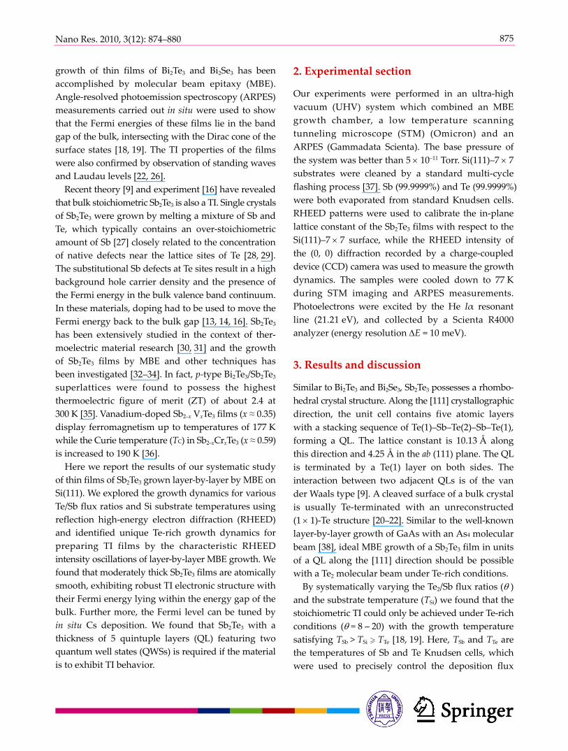
(and thus the ratio) of Sb and Te. The optimized conditions for the fabrication of the Sb2Te3 film were found to be: TSb = 450 °C, TTe = 310 °C, and TSi = 320 °C, resulting in θ ≈ 15 and a growth rate of ~2 QL per minute. In Fig. 1(a), we show the RHEED pattern of a typical Sb2Te3 film with a thickness of 50 QL. The electron beam incidence is along the [110] ( Γ −Κ ) direction. The sharp streaky pattern indicates that the film has an atomically flat surface morphology. The in-plane lattice constant of the 50-QL-films measured from the diffraction pattern with respect to that of Si(111), is 4.26 ± 0.03 Å, consistent with the bulk value of 4.25 Å. Oscillation of the RHEED intensity of the (0, 0) diffraction (the central streak) as a function of growth time is also observed, suggesting a layer-by- layer growth. Here each oscillation corresponds to the deposition of a single QL of Sb2Te3.
A STM image of a typical 50-nm-thick film is shown in Fig. 1(b). The atomically flat morphology is evident.
Figure 1 (a) The RHEED patterns of typical Sb2Te3 films taken along the [110] direction. (b) STM image of the 50-nm-thick film. The image scale is 0.5 μm × 0.5 μm. The insert shows an atomically resolved STM image (2.5 nm × 2.5 nm). (c) ARPES spectra of the 30-nm-thick Sb2Te3 film without doping. (d) ARPES spectra of the 30-nm-thick Sb2Te3 film after depositing 0.1 ML Cs, showing electron-doping of surface states. Both the spectra were taken along the Γ – K direction
The 1 × 1 RHEED pattern and the high resolution STM image with a well-defined 1 × 1 symmetry (insert of Fig. 1(b)) suggest that the growth surface is the Te-terminated Sb2Te3(111)-(1 × 1) surface [20–22]. This surface is similar to that obtained by cleaving a bulk crystal [12–17]. The steps shown in Fig. 1(b) are about 1.0 nm in height, corresponding to 1 QL. As expected, the growth on Si(111) proceeds along the [111] crystallographic direction.
The TI behavior of our MBE grown films was probed by ARPES measurements. In Fig. 1(c) we show the electronic band structure of the 50-nm-thick Sb2Te3 films in the ARPES spectra taken along the Γ −K direction. Besides the broad M-shape valence band (VB) at the bottom, there is an upper linear band dispersion representing the massless Dirac cone and a lower M-shape surface state which is consistent with theoretical calculations [9]. The upper surface state (SS1) and lower surface state (SS2) can be clearly seen around the Γ point as red and blue markers dispersing in the bulk gap. Similar to the bulk crystal, the MBE- grown Sb2Te3 films are also naturally p-type, with the Dirac point located very close to, but slightly above, the Fermi level, making the Dirac point unobservable directly by ARPES measurements. It is interesting to note that, different from the recent ARPES measure- ments on the cleaved (111) surface of the bulk crystal Sb2Te3 [16], our measurements showed that the Fermi energy of the as-grown Sb2Te3 film lies in the energy gap and only intersects the surface Dirac cone, which indicates the film is an intrinsic TI in the absence of doping. Therefore, the fine structure of the surface states and the Dirac cone in the Sb2Te3 film can be observed. In contrast, only large energy scale images of the bulk valence bands without surface state information could be observed in bulk Sb2Te3 crystals [16] since the Fermi energy lies in the bulk valence band continuum. Furthermore, the Sb2Te3 film is found to have very stable bulk and surface states in the ultra high vacuum (UHV) chamber, showing no obvious aging effect or photoinduced doping typical of Bi-based materials [16–19]. The observation indicates that our as-grown Sb2Te3 films are high-quality TIs, containing fewer defects and impurities in comparison with the bulk samples.
Nano Res. 2010, 3(12): 874–880
877
The ability to tune the Fermi level position in a TI is important for electrical transport measurements and device preparation [14]. Surface hole doping of Bi2–xCaxSe3 has been reported by NO2 adsorption [14]. We found that by depositing Cs on a Sb2Te3 film, its Fermi energy was shifted, as shown in Fig. 1(d). Here the Fermi energy is shifted upwards by about 50 meV by depositing about 0.1 monolayer (ML) of Cs. The Dirac point is now clearly visible below the Fermi energy (Fig. 1(d)). Unlike the conventional surface states, the Dirac cone does not change its shape and intensity after the Cs deposition, illustrating that the robustness of the Dirac cone surface states [2–9].
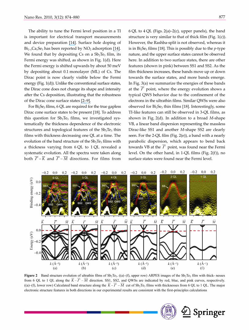
For Bi2Se3 films, 6 QL are required for the true gapless Dirac cone surface states to be present [18]. To address this question for Sb2Te3 films, we investigated sys- tematically the thickness dependence of the electronic structures and topological features of the Sb2Te3 thin films with thickness decreasing one QL at a time. The evolution of the band structure of the Sb2Te3 films with a thickness varying from 6 QL to 1 QL revealed a systematic evolution. All the spectra were taken along both Γ – Κ and Γ − M directions. For films from
6 QL to 4 QL (Figs. 2(a)–2(c), upper panels), the band structure is very similar to that of thick film (Fig. 1(c)). However, the Rashba-split is not observed, whereas it is in Bi2Se3 films [18]. This is possibly due to the p-type nature, and the upper surface states cannot be observed here. In addition to two surface states, there are other features (shown in pink) between SS1 and SS2. As the film thickness increases, these bands move up or down towards the surface states, and more bands emerge. In Fig. 3(a) we summarize the energies of these bands at the Γ point, where the energy evolution shows a typical QWS behavior due to the confinement of the electrons in the ultrathin films. Similar QWSs were also observed for Bi2Se3 thin films [18]. Interestingly, some TI-like features can still be observed in 3-QL films, as shown in Fig. 2(d). In addition to a broad M-shape VB, a linear band dispersion representing the massless Dirac-like SS1 and another M-shape SS2 are clearly seen. For the 2-QL film (Fig. 2(e)), a band with a nearly parabolic dispersion, which appears to bend back towards VB at the Γ point, was found near the Fermi level. On the other hand, in 1-QL films (Fig. 2(f)), no surface states were found near the Fermi level.
Figure 2 Band structure evolution of ultrathin films of Sb2Te3. ((a)–(f), upper row) ARPES images of the Sb2Te3 film with thick- nessesfrom 6 QL to 1 QL along the K – Γ – M direction. SS1, SS2, and QWSs are indicated by red, blue, and pink curves, respectively.((a)–(f), lower row) Calculated band structure along the K – Γ – M cut of Sb2Te3 films with thicknesses from 6 QL to 1 QL. The majorelectronic structure features in both directions in our experimental results are consistent with the first-principles calculations

Nano Res. 2010, 3(12): 874–880
878
Since the surface states above the Fermi level cannot be observed by our ARPES, the thickness at which the gapless Dirac cone forms is difficult to determine by experiment only. Therefore, we carried out first- principles calculations on the thickness-dependent electronic structure. We found an excellent agreement between our experimental data and theoretical calculations (Fig. 2 lower panels). Theoretically, the decay length of the wave functions of the surface states was found to be on the order of 2 nm. The coupling between the surface states from top and bottom sides of the film, which is determined by the penetration depth of the surface-state wave function of a TI, deter- mines the minimum thickness for the TI behavior. Starting from the 5-QL film, the coupling between the two surfaces becomes sufficiently weak, and TI behavior marked by the presence of a single Dirac- cone surface state was found to emerge. Moreover, the Fermi velocity can be calculated from the band structure. In Fig. 3(b), we plot the Fermi velocity and the position of the Dirac point for different films. Both the Fermi velocity and the Dirac point position are already close to the bulk value at a thickness of 6 QL. The Fermi velocity from our measurements is about 4.4 × 10⁵ m/s, which agrees well with the results of our theoretical calculations.
In the spectra of the very thick Sb2Te3 film (Fig. 1(c)), we can hardly observe the bulk band which should evolve from the QWSs. The reason is that the states in bulk bands become 3-D, and thus can only appear in photoemission spectra at a certain photon energy which connects the initial and final states. Since in our measurements, only one photon energy (21.21 eV) is used—which may not satisfy the emission condition— the absence of the bulk bands in ARPES spectra is to be expected.
The systematic behavior observed above suggests that two QWSs are necessary for the observation of TI in a film. QWSs are formed in ultrathin films because of the confinement of the movement of electrons. For atomically flat thin films grown on Si(111), QWSs have been found to give rise to many novel properties [39, 40]. Clearly, the QWSs observed in our Sb2Te3 films also originate from quantum confinement. Here the electrons come from the valence bands rather than conduction bands—as observed previously in metal films. Interestingly, it appears that at least two QWSs are needed for a TI film to host Dirac cone surface states. Typically electrons confined in a thin film or an interface system are considered quasi two-dimensional (2-D) as long as only the lowest quantum state is occupied. Therefore when two QWSs are occupied in
Figure 3 (a) Thickness-dependent normal emission ARPES spectra of Sb2Te3 films with different thicknesses. QWS peaks are markedby arrows. (b) Thickness-dependent Fermi velocities and Dirac points of thin films of Sb2Te3. The Fermi velocity was measured byfitting the experimental dispersion with E = ħVFK

Nano Res. 2010, 3(12): 874–880
879
a film, which corresponds to a thickness of about 5 nm for our Sb2Te3 films, the electrons in the film cease to be quasi 2-D. On the other hand, it is surprising that 3-D topological properties persist when only two QWSs are occupied. Indeed, for Bi2Se3 films, even though two QWSs were found for a film as thin as 3 QL, a Dirac cone was found only when the film thickness reaches a minimum of 6 QL with two QWSs [18]. Therefore, the presence of two QWSs must be a necessary, but not sufficient condition, for a film to show TI behavior.
4. Conclusions
We have demonstrated experimentally that atomically flat, single-crystalline, and—to date—the thinnest TI can be prepared by depositing Sb2Te3 onto Si(111) using MBE. The as-grown thick Sb2Te3 films exhibit robust TI behavior with their Fermi energy intersecting only the Dirac cone of the surface states. The Fermi energy of the Sb2Te3 film was tuned by in situ Cs deposition. Thickness-dependent ARPES studies and first-principles calculations showed that a thickness of 5 QL for Sb2Te3 films featuring two QWSs is required for the presence of TI behavior.
Acknowledgements
The work is supported by the National Natural Science Foundation of China (NSFC) and the National Basic Research Program of the Ministry of Science and Technology of China (MOST). Work at Pennsylvania State University is supported by the National Science Foundation (NSF) under Grant No. DMR 0908700.
Open Access: This article is distributed under the terms of the Creative Commons Attribution Noncommercial License which permits any noncommercial use, distribution, and reproduction in any medium, provided the original author(s) and source are credited.
References
[1] Casto Neto, A. H.; Guinea, F.; Peres, N. M. R.; Novoselov, K. S.; Geim, A. K. The electronic properties of graphene. Rev. Mod. Phys. 2009, 81, 109–162.
[2] Bernevig, B. A.; Zhang, S. C. Quantum spin Hall effect. Phys. Rev. Lett. 2006, 96, 106802.
[3] König, M.; Wiedmann, S.; Brüne, C.; Roth, A.; Buhmann, H.; Molenkamp, L. W.; Qi, X. L.; Zhang, S. C. Quantum spin Hall insulator state in HgTe quantum wells. Science 2007, 318, 766–770.
[4] Fu, L.; Kane, C. L.; Mele, E. J. Topological insulators in three dimensions. Phys. Rev. Lett. 2007, 98, 106803.
[5] Moore, J. E.; Balents, L. Topological invariants of time- reversal-invariant band structures. Phys. Rev. B 2007, 75, 121306.
[6] Fu, L.; Kane, C. L. Topological insulators with inversion symmetry. Phys. Rev. B 2007, 76, 045302.
[7] Qi, X. L.; Hughes, T. L.; Zhang, S. C. Topological field theory of time-reversal invariant insulators. Phys. Rev. B 2007, 78, 195424.
[8] Qi, X. L.; Li, R. D.; Zang, J. D.; Zhang, S. C. Inducing a magnetic monopole with topological surface states. Science 2009, 323, 1184–1187.
[9] Zhang, H. J.; Liu, C. X.; Qi, X. L.; Dai, X.; Fang, Z.; Zhang, S. C. Topological insulators in Bi2Se3, Bi2Te3, and Sb2Te3
with a single Dirac cone on the surface. Nat. Phys. 2009, 5, 438–442.
[10] Hsieh, D.; Qian, D.; Wray, L.; Xia, Y.; Hor, Y. S.; Cava, R. J.; Hasan, M. Z. A topological Dirac insulator in a quantum spin Hall phase. Nature 2008, 452, 970–974.
[11] Hsieh, D.; Xia, Y.; Wray, L.; Qian, D.; Pal, A.; Dil, J. H.; Osterwalder, J.; Meier, F.; Bihlmayer, G.; Kane, C. L.; Hor, Y. S.; Cava, R. J.; Hasan, M. Z. Observation of unconventional quantum spin textures in topological insulators. Science 2009, 323, 919–922.
[12] Xia, Y.; Qian, D.; Hsieh, D.; Wray, L.; Pal, A.; Lin, H.; Bansil, A.; Grauer, D.; Hor, Y. S.; Cava, R. J.; Hasan, M. Z. Observation of a large-gap topological-insulator class with a single Dirac cone on the surface. Nat. Phys. 2009, 5, 398–402.
[13] Chen, Y. L.; Analytis, J. G.; Chu, J. H.; Liu, Z. K.; Mo, S. K.; Qi, X. L.; Zhang, H. J.; Lu, D. H.; Dai, X.; Fang, Z.; Zhang, S. C.; Fisher, I. R.; Hussain, Z.; Shen, Z. X. Experimental realization of a three-dimensional topological insulator, Bi2Te3. Science 2009, 325, 178–181.
[14] Hsieh, D.; Xia, Y.; Qian, D.; Wray, L.; Dil, J. H.; Meier, F.; Osterwalder, J.; Patthey, L.; Checkelsky, J. G.; Ong, N. P.; Fedorov, A. V.; Lin, H.; Bansil, A.; Grauer, D.; Hor, Y. S.; Cava, R. J.; Hasan, M. Z. A tunable topological insulator in the spin helical Dirac transport regime. Nature 2009, 460, 1101–1105.
[15] Hor, Y. S.; Richardella, A.; Roushan, P.; Xia, Y.; Checkelsky, J. G.; Yazdani, A.; Hasan, M. Z.; Ong, N. P.; Cava, R. J. p-type Bi2Se3 for topological insulator and low-temperature thermoelectric applications. Phys. Rev. B 2009, 79, 195208.
[16] Hsieh, D.; Xia, Y.; Qian, D.; Wray, L.; Meier, F.; Dil, J. H.; Osterwalder, J.; Patthey, L.; Fedorov, A. V.; Lin, H.; Bansil, A.; Grauer, D.; Hor, Y. S.; Cava, R. J.; Hasan, M. Z. Observation

Nano Res. 2010, 3(12): 874–880
880
of time-reversal-protected single-Dirac-cone topological- insulator states in Bi2Te3 and Sb2Te3. Phys. Rev. Lett. 2009, 103, 146401.
[17] Xia, Y.; Qian, D.; Hsieh, D.; Shankar, R.; Lin, H.; Bansil, A.; Fedorov, A. V.; Grauer, D.; Hor, Y. S.; Cava, R. J.; Hasan, M. Z. Topological control: Systematic control of topological insulator Dirac fermion density on the surface of Bi2Te3. Preprint at http://arxiv.org/abs/0907.3089 (2009).
[18] Zhang, Y.; He, K.; Chang, C. Z.; Song, C. L.; Wang, L. L.; Chen, X.; Jia, J. F.; Fang, Z.; Dai, X.; Shan, W. Y.; Shen, S. Q.; Niu, Q.; Qi, X. L.; Zhang, S. C.; Ma, X. C.; Xue, Q. K. Crossover of the three-dimensional topological insulator Bi2Se3 to the two-dimensional limit. Nat. Phys. 2010, 6, 584–588.
[19] Li, Y. Y.; Wang, G.; Zhu, X. G.; Liu, M. H.; Ye, C.; Chen, X.; Wang, Y. Y.; He, K.; Wang, L. L.; Ma, X. C.; Zhang, H. J.; Dai, X.; Fang, Z.; Liu, Y.; Qi, X. L.; Jia, J. F.; Zhang, S. C.; Xue, Q. K. Intrinsic topological insulator Bi2Te3 thin films on Si and their thickness limit. Adv. Mater. 2010, 22, 4002–4007.
[20] Urazhdin, S.; Bilc, D.; Tessmer, S. H.; Mahanti, S. D.; Kyratsi, T.; Kanatzidis, M. G. Scanning tunneling microscopy of defect states in the semiconductor Bi2Se3. Phys. Rev. B 2002, 66, 161306.
[21] Urazhdin, S.; Bilc, D.; Tessmer, S. H.; Mahanti, S. D.; Kyratsi, T.; Kanatzidis, M. G. Surface effects in layered semiconductors Bi2Se3 and Bi2Te3. Phys. Rev. B 2004, 69, 085313.
[22] Zhang, T.; Cheng, P.; Chen, X.; Jia, J. F.; Ma, X. C.; He, K.; Wang, L. L.; Zhang, H. J.; Dai, X.; Fang, Z.; Xie, X. C.; Xue, Q. K. Experimental demonstration of topological surface states protected by time-reversal symmetry. Phys. Rev. Lett. 2009, 103, 266803.
[23] Zhang, G. H.; Qin, H. J.; Teng, J.; Guo, J. D.; Guo, Q. L.; Dai, X.; Fang, Z.; Wu, K. H. Quintuple-layer epitaxy of thin films of topological insulator Bi2Se3. Appl. Phys. Lett. 2009, 95, 053114.
[24] Roushan, P.; Seo, J.; Parker, C. V.; Hor, Y. S.; Hsieh, D.; Qian, D.; Richardella, A.; Hasan, M. Z.; Cava, R. J.; Yazdani, A. Topological surface states protected from backscattering by chiral spin texture. Nature 2009, 460, 1106–1109.
[25] Alpichshev, Z.; Analyits, J. G.; Chu, J. H.; Fisher, I. R.; Chen, Y. L.; Shen, Z. X.; Fang, A.; Kapitulnik, A. STM imaging of electronic waves on the surface of Bi2Te3: Topologically protected surface states and hexagonal warping effects. Phys. Rev. Lett. 2010, 104, 016401.
[26] Cheng, P.; Song, C. L.; Zhang, T.; Zhang, Y. Y.; Wang, Y. L.; Jia, J. F.; Wang, J.; Wang, Y. Y.; Zhu, B. F.; Chen, X.; Ma, X. C.; He, K.; Wang, L. L.; Dai, X.; Fang, Z.; Xie, X. C.; Qi, X. L.; Liu, C. X.; Zhang, S. C.; Xue, Q. K. Landau quantization of topological surface states in Bi2Se3. Phys. Rev. Lett. 2010, 105, 076801.
[27] Abrikosov, N.; Poretskaya, L.; Ivanova, I. Investigation of the Sb–Te system. Zh. Neorg. Khim. 1959, 4(11), 2525–2531 (in Russian). TR: Russ. J. Inorganic Chem., 1959, 4(11), 1163–1166.
[28] Horak, J.; Tichy, L.; Lostak, P.; Vasko, A. Lattice-defects in iodine-doped Sb2Te3 and Bi2Te3 crystals. Cryst. Latt. Def. 1976, 6, 233–238.
[29] Horak, J.; Cermak, K.; Koudelka, L. Energy formation of antisite defects in doped Sb2Te3 and Bi2Te3 crystals. J. Phys. Chem. Solids 1986, 47, 805–809.
[30] Simon, G.; Eichler, W. Y. Galvanomagnetische und ther- moelektrische transportuntersuchungen an Sb2Te3. Phys. Status Solidi B 1981, 103, 289–295.
[31] Stordeur, M.; Simon, G. Investigation of the weak-field charge transport in semiconducting V2–VI3 compounds with trigonal symmetry II. Interpretation of the weak-field charge transport in Sb2Te3 single crystals. Phys. Status Solidi B 1984, 124, 799–806.
[32] Chien, Y. J.; Zhou, Z. H.; Uher, C. Growth and transport properties of Sb2−xVxTe3 thin films on sapphire substrates. J. Cryst. Growth 2005, 283, 309–314.
[33] Venkatasubramanian, R.; Colpitts, T.; Watko, E.; Lamvik, M.; EI-Masry, N. MOCVD of Bi2Te3, Sb2Te3 and their superlattice structures for thin-film thermoelectric applications. J. Cryst. Growth 1997, 170, 817–821.
[34] Iwata, Y.; Kobayashi, H.; Kikuchi, S.; Hatta, E.; Mukasa, K. In situ reflection high-energy electron diffraction (RHEED) observation of Bi2Te3/Sb2Te3 multilayer film growth. J. Cryst. Growth 1999, 203, 125–130.
[35] Venkatasubramanian, R.; Siivola, E.; Colpitts, T.; O’Quinn, B. Thin-film thermoelectric devices with high room- temperature figures of merit. Nature 2001, 413, 597–602.
[36] Chien, Y. J. Transition metal-doped Sb2Te3 and Bi2Te3 diluted magnetic semiconductors. Ph.D. Dissertation, University of Michigan, USA, 2007.
[37] Li, J. L.; Jia, J. F.; Liang, X. J.; Liu, X.; Wang, J. Z.; Xue, Q. K.; Li, Z. Q.; Tse, J. S.; Zhang, Z. Y.; Zhang, S. B. Spontaneous assembly of perfectly ordered identical-size nanocluster arrays. Phys. Rev Lett. 2002, 88, 066101.
[38] Xue, Q. K.; Hashizume, T.; Sakurai, T. Scanning tunneling microscopy of III–V compound semiconductor (001) surfaces. Prog. Surf. Sci. 1997, 56, 1–131.
[39] Guo, Y.; Zhang, Y. F.; Bao, X. Y.; Han, T. Z.; Tang, Z.; Zhang, L. X.; Zhu, W. G.; Wang, E. G.; Niu, Q.; Qiu, Z. Q.; Jia, J. F.; Zhao, Z. X.; Xue, Q. K. Superconductivity modulated by quantum size effects. Science 2004, 306, 1915–1917.
[40] Jia, J. F.; Li, S. C.; Zhang, Y. F.; Xue, Q. K. Quantum size effects induced novel properties in two-dimensional electronic systems: Pb thin films on Si(111). J. Phys. Soc. Jpn. 2007, 76, 082001.
Copyright © 2022 FDOKUMEN