Low voltage vertical organic field-effect transistor with polyvinyl alcohol as gate insulator
6
Low voltage vertical organic field-effect transistor with polyvinyl alcohol as gate insulator Lucieli Rossi, Keli F. Seidel, Wagner S. Machado, and Ivo A. Hümmelgen Citation: Journal of Applied Physics 110, 094508 (2011); doi: 10.1063/1.3660406 View online: http://dx.doi.org/10.1063/1.3660406 View Table of Contents: http://scitation.aip.org/content/aip/journal/jap/110/9?ver=pdfcov Published by the AIP Publishing Articles you may be interested in Modeling of a vertical tunneling graphene heterojunction field-effect transistor Appl. Phys. Lett. 101, 033503 (2012); 10.1063/1.4737394 Low- organic layer as a top gate dielectric for graphene field effect transistors Appl. Phys. Lett. 100, 193117 (2012); 10.1063/1.4711776 Solution-processible high-permittivity nanocomposite gate insulators for organic field-effect transistors Appl. Phys. Lett. 93, 013302 (2008); 10.1063/1.2949320 Hysteresis-free organic field-effect transistors and inverters using photocrosslinkable poly(vinyl cinnamate) as a gate dielectric Appl. Phys. Lett. 92, 143306 (2008); 10.1063/1.2907974 Static model for organic field-effect transistors including both gate-voltage-dependent mobility and depletion effect Appl. Phys. Lett. 88, 233514 (2006); 10.1063/1.2211148 [This article is copyrighted as indicated in the article. Reuse of AIP content is subject to the terms at: http://scitation.aip.org/termsconditions. Downloaded to ] IP: 200.19.73.233 On: Fri, 04 Apr 2014 13:57:15
-
Upload
independent -
Category
Documents
-
view
1 -
download
0
Transcript of Low voltage vertical organic field-effect transistor with polyvinyl alcohol as gate insulator

Low voltage vertical organic field-effect transistor with polyvinyl alcohol as gateinsulatorLucieli Rossi, Keli F. Seidel, Wagner S. Machado, and Ivo A. Hümmelgen
Citation: Journal of Applied Physics 110, 094508 (2011); doi: 10.1063/1.3660406 View online: http://dx.doi.org/10.1063/1.3660406 View Table of Contents: http://scitation.aip.org/content/aip/journal/jap/110/9?ver=pdfcov Published by the AIP Publishing Articles you may be interested in Modeling of a vertical tunneling graphene heterojunction field-effect transistor Appl. Phys. Lett. 101, 033503 (2012); 10.1063/1.4737394 Low- organic layer as a top gate dielectric for graphene field effect transistors Appl. Phys. Lett. 100, 193117 (2012); 10.1063/1.4711776 Solution-processible high-permittivity nanocomposite gate insulators for organic field-effect transistors Appl. Phys. Lett. 93, 013302 (2008); 10.1063/1.2949320 Hysteresis-free organic field-effect transistors and inverters using photocrosslinkable poly(vinyl cinnamate) as agate dielectric Appl. Phys. Lett. 92, 143306 (2008); 10.1063/1.2907974 Static model for organic field-effect transistors including both gate-voltage-dependent mobility and depletioneffect Appl. Phys. Lett. 88, 233514 (2006); 10.1063/1.2211148
[This article is copyrighted as indicated in the article. Reuse of AIP content is subject to the terms at: http://scitation.aip.org/termsconditions. Downloaded to ] IP:
200.19.73.233 On: Fri, 04 Apr 2014 13:57:15
Low voltage vertical organic field-effect transistor with polyvinyl alcoholas gate insulator
Lucieli Rossi, Keli F. Seidel, Wagner S. Machado, and Ivo A. Hummelgena)
Departamento de Fısica, Universidade Federal do Parana, Caixa Postal 19044, 81531-980 Curitiba PR,Brazil
(Received 8 July 2011; accepted 7 October 2011; published online 8 November 2011)
We report the preparation of low gate leakage current organic field effect transistors in vertical
architecture using polyvinyl alcohol as gate insulator and C60 fullerene as n-type semiconductor
in devices with gate, source, and drain electrodes of Al. Intermediate electrode and top electrode
operate, respectively, as source and drain, or vice-versa, depending on polarity. In these devices the
intermediate electrode (source or drain) is permeable to the electric field produced by the gate so
that increased drain current is obtained at either increasingly negative gate voltage when the source
is the intermediate electrode or increasingly positive gate voltage when the drain is the intermediate
electrode. VC 2011 American Institute of Physics. [doi:10.1063/1.3660406]
INTRODUCTION
A significant effort has been made in the last years to
develop organic field effect transistors able to operate at low
voltages. Due to the low mobility of charge carriers in or-
ganic semiconductors, the conventional field-effect transistor
(FET) geometry originally proposed by Lilienfeld1 usually
imposes some constraints to transistor operational character-
istics, like high operational voltage and long response times
due to the long pathways of the charge carriers along the
transistor channel.
In order to reduce the distances covered by charge car-
riers in the semiconductor, vertical transistor architectures
like the permeable-base2,3 and metal-base transistor,4,5 origi-
nally proposed for inorganic semiconductors, were also
successfully applied to organic semiconductors, allowing
operation at low voltages (< 5 V),6,7 obtaining current gain
and even reasonably high unitary gain frequencies, of the
order of 170 kHz.8 Additional vertically structured organic
transistor architectures, like static induction transistor9 and
space-charge limited transistor10 were also demonstrated in
the effort to develop this type of device architecture in
organic electronics.
A few years ago, vertical field-effect transistors
(VFETs) in which essentially a capacitor and an organic
semiconductor diode were stacked in a tandem structure and
showing one common electrode were reported.11–13 In these
devices LiF was employed as gate insulator. It was proposed
that this material should be advantageous due to the high ca-
pacitance of the capacitor part of the device, which would
also be a requirement for the proper operation of devices
constructed in this structure. One serious drawback presented
by these LiF devices was the large leakage current of the ca-
pacitor,11 corresponding to a high gate current in the FET,
which under such conditions practically operate much more
as a two-terminal device. The same architecture was also
more recently used for organic light-emitting transistors on
plastic,14 SiO2-gate transistors with carbon nanotubes for
charge injection enhancement15 and transistors based on
other material combinations.16–19
Apart from the above cited problem, the use of LiF as a
gate insulator implies in high gate capacitance, which is a
necessary characteristic in the conventional architecture or-
ganic FETs for the conducting channel formation. This high
capacitance, however, results high RC time constant values
when the device is operated, with a consequent limitation of
the frequency at which such devices can be switched
or modulated, so that insulator options are welcome for this
structures, especially those compatible with flexible
substrates.
In this article, we report the preparation of VFETs pre-
pared sequentially depositing Al (the gate terminal), polyvi-
nyl alcohol (PVA), Al (source or drain), C60 and Al (source
or drain).
EXPERIMENTAL
The devices were prepared depositing a 100 nm thick
Al (Aldrich,> 99.99%) bottom gate (G) electrode at a
base pressure of 10�6 Torr by thermal evaporation, at
�20 nm s�1 onto previously cleaned glass substrate. In the
sequence, the gate insulator, a 250 nm thick PVA (Fluka,
MW¼ 130.000) layer was deposited from a 50 mg=mL PVA
solution in ultrapure water by spin coating at 1500 rpm dur-
ing 60 s. After this procedure the sample was annealed at
130 �C during 60 min and then during 4 h at 60 �C in
vacuum, following a procedure described by Sun et al.20
The further step was a 20 nm Al electrode deposition, at
�4 nm s�1. This layer is very thin to allow electric field per-
meability,21 and this characteristic tends to imply in high
electrical resistance. But high resistance results serious per-
formance degradation due to the voltage drop along the film
in the path to the wire connecting point. To assuage this
problem we also prepared devices in which an additional
100 nm Al (�20 nm s�1) layer was evaporated on top of the
a)Author to whom correspondence should be addressed. Electronic mail:
[email protected]. Fax: þ55-41-33613645.
0021-8979/2011/110(9)/094508/5/$30.00 VC 2011 American Institute of Physics110, 094508-1
JOURNAL OF APPLIED PHYSICS 110, 094508 (2011)
[This article is copyrighted as indicated in the article. Reuse of AIP content is subject to the terms at: http://scitation.aip.org/termsconditions. Downloaded to ] IP:
200.19.73.233 On: Fri, 04 Apr 2014 13:57:15
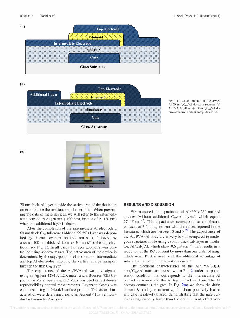
20 nm thick Al layer outside the active area of the device in
order to reduce the resistance of this terminal. When present-
ing the date of these devices, we will refer to the intermedi-
ate electrode as Al (20 nmþ 100 nm), instead of Al (20 nm)
when this additional layer is absent.
After the completion of the intermediate Al electrode a
60 nm thick C60 fullerene (Aldrich, 99.5%) layer was depos-
ited by thermal evaporation (�4 nm s�1), followed by
another 100 nm thick Al layer (�20 nm s�1), the top elec-
trode (see Fig. 1). In all cases the layer geometry was con-
trolled using shadow masks. The active area of the device is
determined by the superposition of the bottom, intermediate
and top Al electrodes, allowing the vertical charge transport
through the thin C60 layer.
The capacitance of the Al=PVA=Al was investigated
using an Agilent 4284 A LCR meter and a Boonton 72B Ca-
pacitance Meter operating at 2 MHz was used in fast device
reproducibility control measurements. Layers thickness was
estimated using a Dektak3 surface profiler. Transistor char-
acteristics were determined using an Agilent 4155 Semicon-
ductor Parameter Analyzer.
RESULTS AND DISCUSSION
We measured the capacitance of Al=PVA(250 nm)=Al
devices (without additional C60=Al layers), which equals
27 nF cm�2. This capacitance corresponds to a dielectric
constant of 7.6, in agreement with the values reported in the
literature, which are between 5 and 8.22 The capacitance of
the Al=PVA=Al structure is very low if compared to analo-
gous structures made using 230 nm thick LiF layer as insula-
tor, Al=LiF=Al, which show 0.6 lF cm�2. This results in a
reduction of the RC constant by more than one order of mag-
nitude when PVA is used, with the additional advantage of
substantial reduction in the leakage current.
The electrical characteristics of the Al=PVA=Al(20
nm)=C60=Al transistor are shown in Fig. 2 under the polar-
ization condition that corresponds to the intermediate Al
contact as source and the Al top contact as drain. The Al
bottom contact is the gate. In Fig. 2(a) we show the drain
current ID and gate current IG for drain positively biased
and gate negatively biased, demonstrating that the gate cur-
rent is significantly lower than the drain current, effectively
FIG. 1. (Color online) (a) Al/PVA/
Al(20 nm)/C60/Al device structure; (b)
Al/PVA/Al(20 nmþ 100 nm)/C60/Al de-
vice structure; and (c) complete device.
094508-2 Rossi et al. J. Appl. Phys. 110, 094508 (2011)
[This article is copyrighted as indicated in the article. Reuse of AIP content is subject to the terms at: http://scitation.aip.org/termsconditions. Downloaded to ] IP:
200.19.73.233 On: Fri, 04 Apr 2014 13:57:15
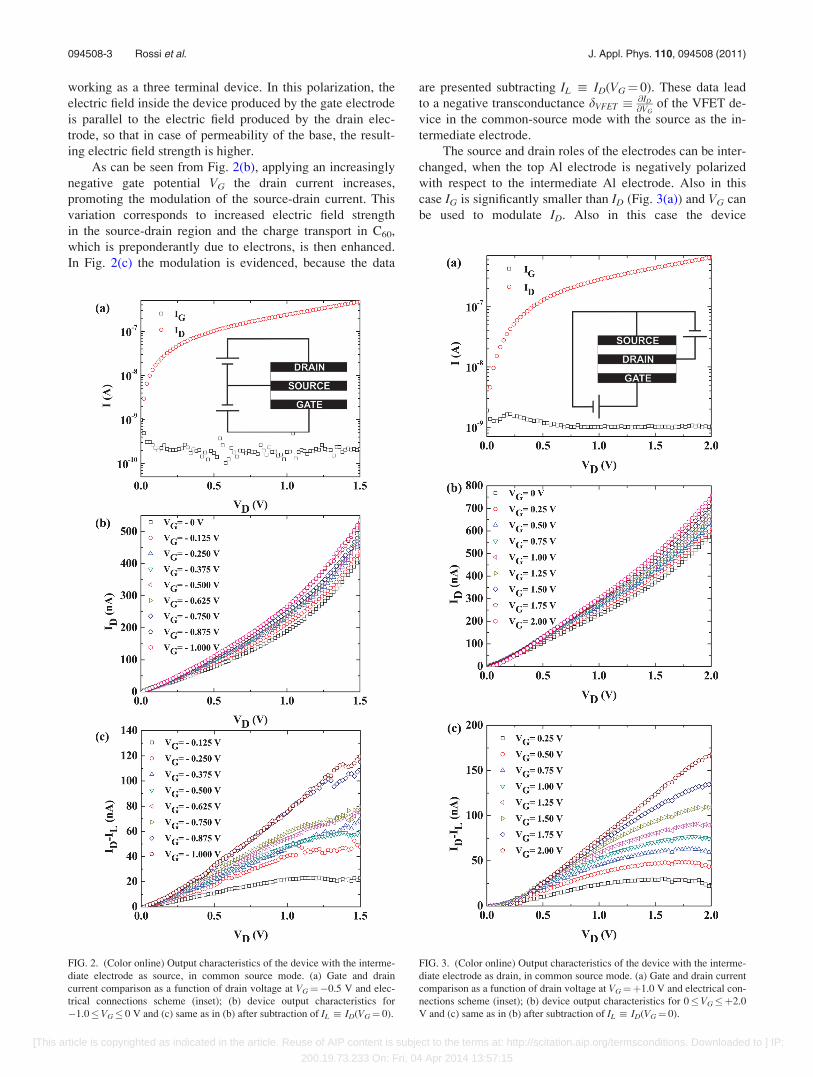
working as a three terminal device. In this polarization, the
electric field inside the device produced by the gate electrode
is parallel to the electric field produced by the drain elec-
trode, so that in case of permeability of the base, the result-
ing electric field strength is higher.
As can be seen from Fig. 2(b), applying an increasingly
negative gate potential VG the drain current increases,
promoting the modulation of the source-drain current. This
variation corresponds to increased electric field strength
in the source-drain region and the charge transport in C60,
which is preponderantly due to electrons, is then enhanced.
In Fig. 2(c) the modulation is evidenced, because the data
are presented subtracting IL : ID(VG¼ 0). These data lead
to a negative transconductance dVFET � @ID
@VGof the VFET de-
vice in the common-source mode with the source as the in-
termediate electrode.
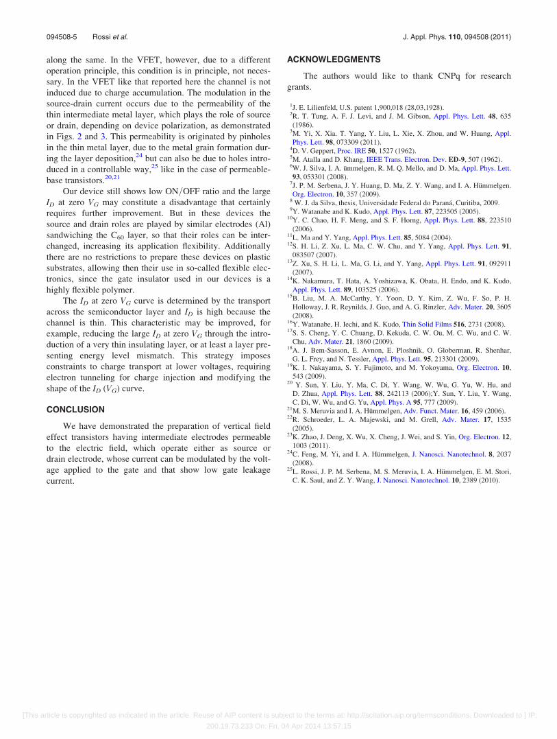
The source and drain roles of the electrodes can be inter-
changed, when the top Al electrode is negatively polarized
with respect to the intermediate Al electrode. Also in this
case IG is significantly smaller than ID (Fig. 3(a)) and VG can
be used to modulate ID. Also in this case the device
FIG. 2. (Color online) Output characteristics of the device with the interme-
diate electrode as source, in common source mode. (a) Gate and drain
current comparison as a function of drain voltage at VG¼�0.5 V and elec-
trical connections scheme (inset); (b) device output characteristics for
�1.0�VG� 0 V and (c) same as in (b) after subtraction of IL : ID(VG¼ 0).
FIG. 3. (Color online) Output characteristics of the device with the interme-
diate electrode as drain, in common source mode. (a) Gate and drain current
comparison as a function of drain voltage at VG¼þ1.0 V and electrical con-
nections scheme (inset); (b) device output characteristics for 0�VG�þ2.0
V and (c) same as in (b) after subtraction of IL : ID(VG¼ 0).
094508-3 Rossi et al. J. Appl. Phys. 110, 094508 (2011)
[This article is copyrighted as indicated in the article. Reuse of AIP content is subject to the terms at: http://scitation.aip.org/termsconditions. Downloaded to ] IP:
200.19.73.233 On: Fri, 04 Apr 2014 13:57:15

polarization corresponds to parallel electric fields, and posi-
tive VG increases ID leading to a positive transconductance
of the VFET device in the common-source mode with the
drain as the intermediate electrode and source as top elec-
trode. In this case VG is positive and due to the change in the
orientation of the electric field between source and drain and
the effect of the electric field produced by the gate remains
additive.
The dependence of the drain current on gate voltage
(shown in Fig. 4) of our VFETs differs from that shown in
planar FETs. The transconductance dVFET � @ID
@VGis dependent
on gate voltage, dVFETj j increasing with increasing VGj j. This
is due to the charge transport in the C60 layer, space-charge
limited current (characterized by I / V2), which leads to a
linear dependence offfiffiffiffiffiID
pon VD at VG¼ 0 for larger VD val-
ues, like shown in Fig. 5. Due to this dependence and the
additive character of the electric filed produced by drain and
gate voltages for large gate voltages, the ID(VG) curve, like
presented in Fig. 4, should also progressively tend to a para-
bolic dependence.
The constructive field modulation in the case of the de-
vice with intermediate source electrode, expressed as a nega-
tive transconductance in that case, differs from that observed
in other VFET devices,11,18 polarized in common-source
mode (like in Fig. 2), which show positive transconductance.
In our devices the electric field produced by the gate enhan-
ces the electric field produced by the drain, so that the source
effectively acts as a grid, which is permeable to the electric
field. Positive transconductance in such a configuration, by
the other way, requires a more complex mechanism, includ-
ing polarization of the dielectric medium and charge com-
pensation by the source, with a thickness less than the
electrostatic screening length of the source material, to
explain the device operational characteristics.
It is evident that the current magnitude as well as the
modulation capability of the devices like those presented in
Figs. 2 and 3 are too low. To overcome this difficulty, we
prepared devices with the additional 100 nm thick Al layer
in the intermediate electrode, as explained in the previous
section. These Al=PVA=Al(20 nmþ 100 nm)=C60=Al devi-
ces can also be modulated using both, positive and negative
gate polarization, as demonstrated in Fig. 6, which shows the
drain current variation as a function of gate voltage. In this
device, the second Al layer (100 nm) of the intermediate
electrode was evaporated so that the distance to the active
area of the devices was 100 lm. As a consequence the ID
current and modulation amplitude can be improved, reducing
the resistance of the intermediate metal terminal. Since one
requirement of this terminal is the permeability to the elec-
tric field, the thin metallic layer must be restricted to a mini-
mum, exceeding as less as possible the active device area.
Apart from the strategy used here, it is worth to mention
that other strategies were reported to allow the preparation of
thicker metal layers still presenting permeable character, not
showing too high in-plane resistance, like the co-evaporation
of the metal and the organic semiconductor during the per-
meable electrode preparation.23
The use of PVA as an insulator layer reduces the capaci-
tance of the gate with a consequent reduction of the RC time
constant. In the case of the conventional FET, the high
capacitance is necessary because it corresponds to a high dis-
placement of charges in the channel, inducing conductivity
FIG. 6. (Color online) Output characteristics of the Al=PVA=Al
(20 nmþ 100 nm)=C60=Al device with the intermediate electrode as source,
in common source mode, for �1.5�VD� 0 V after subtraction of
IL: ID(VG¼0).
FIG. 4. VFET transference curve at VD¼�0.48 V. Device with the interme-
diate electrode as source, in common source mode.
FIG. 5. (Color online) Plot of the ID(VD) dependence, evidencing the space-
charge limited current characterized by I / V2. The open circles correspond
to experimental data and the red straight line corresponds to
@I1=2D
�VD ¼ 1:0. The device configuration is the same as in Fig. 3.
094508-4 Rossi et al. J. Appl. Phys. 110, 094508 (2011)
[This article is copyrighted as indicated in the article. Reuse of AIP content is subject to the terms at: http://scitation.aip.org/termsconditions. Downloaded to ] IP:
200.19.73.233 On: Fri, 04 Apr 2014 13:57:15
along the same. In the VFET, however, due to a different
operation principle, this condition is in principle, not neces-
sary. In the VFET like that reported here the channel is not
induced due to charge accumulation. The modulation in the
source-drain current occurs due to the permeability of the
thin intermediate metal layer, which plays the role of source
or drain, depending on device polarization, as demonstrated
in Figs. 2 and 3. This permeability is originated by pinholes
in the thin metal layer, due to the metal grain formation dur-
ing the layer deposition,24 but can also be due to holes intro-
duced in a controllable way,25 like in the case of permeable-
base transistors.20,21
Our device still shows low ON=OFF ratio and the large
ID at zero VG may constitute a disadvantage that certainly
requires further improvement. But in these devices the
source and drain roles are played by similar electrodes (Al)
sandwiching the C60 layer, so that their roles can be inter-
changed, increasing its application flexibility. Additionally
there are no restrictions to prepare these devices on plastic
substrates, allowing then their use in so-called flexible elec-
tronics, since the gate insulator used in our devices is a
highly flexible polymer.
The ID at zero VG curve is determined by the transport
across the semiconductor layer and ID is high because the
channel is thin. This characteristic may be improved, for
example, reducing the large ID at zero VG through the intro-
duction of a very thin insulating layer, or at least a layer pre-
senting energy level mismatch. This strategy imposes
constraints to charge transport at lower voltages, requiring
electron tunneling for charge injection and modifying the
shape of the ID (VG) curve.
CONCLUSION
We have demonstrated the preparation of vertical field
effect transistors having intermediate electrodes permeable
to the electric field, which operate either as source or
drain electrode, whose current can be modulated by the volt-
age applied to the gate and that show low gate leakage
current.
ACKNOWLEDGMENTS
The authors would like to thank CNPq for research
grants.
1J. E. Lilienfeld, U.S. patent 1,900,018 (28,03,1928).2R. T. Tung, A. F. J. Levi, and J. M. Gibson, Appl. Phys. Lett. 48, 635
(1986).3M. Yi, X. Xia. T. Yang, Y. Liu, L. Xie, X. Zhou, and W. Huang, Appl.
Phys. Lett. 98, 073309 (2011).4D. V. Geppert, Proc. IRE 50, 1527 (1962).5M. Atalla and D. Khang, IEEE Trans. Electron. Dev. ED-9, 507 (1962).6W. J. Silva, I. A. ummelgen, R. M. Q. Mello, and D. Ma, Appl. Phys. Lett.
93, 053301 (2008).7J. P. M. Serbena, J. Y. Huang, D. Ma, Z. Y. Wang, and I. A. Hummelgen.
Org. Electron. 10, 357 (2009).8 W. J. da Silva, thesis, Universidade Federal do Parana, Curitiba, 2009.9Y. Watanabe and K. Kudo, Appl. Phys. Lett. 87, 223505 (2005).
10Y. C. Chao, H. F. Meng, and S. F. Horng, Appl. Phys. Lett. 88, 223510
(2006).11L. Ma and Y. Yang, Appl. Phys. Lett. 85, 5084 (2004).12S. H. Li, Z. Xu, L. Ma, C. W. Chu, and Y. Yang, Appl. Phys. Lett. 91,
083507 (2007).13Z. Xu, S. H. Li, L. Ma, G. Li, and Y. Yang, Appl. Phys. Lett. 91, 092911
(2007).14K. Nakamura, T. Hata, A. Yoshizawa, K. Obata, H. Endo, and K. Kudo,
Appl. Phys. Lett. 89, 103525 (2006).15B. Liu, M. A. McCarthy, Y. Yoon, D. Y. Kim, Z. Wu, F. So, P. H.
Holloway, J. R. Reynilds, J. Guo, and A. G. Rinzler, Adv. Mater. 20, 3605
(2008).16Y. Watanabe, H. Iechi, and K. Kudo, Thin Solid Films 516, 2731 (2008).17S. S. Cheng, Y. C. Chuang, D. Kekuda, C. W. Ou, M. C. Wu, and C. W.
Chu, Adv. Mater. 21, 1860 (2009).18A. J. Bem-Sasson, E. Avnon, E. Ploshnik, O. Globerman, R. Shenhar,
G. L. Frey, and N. Tessler, Appl. Phys. Lett. 95, 213301 (2009).19K. I. Nakayama, S. Y. Fujimoto, and M. Yokoyama, Org. Electron. 10,
543 (2009).20 Y. Sun, Y. Liu, Y. Ma, C. Di, Y. Wang, W. Wu, G. Yu, W. Hu, and
D. Zhua, Appl. Phys. Lett. 88, 242113 (2006);Y. Sun, Y. Liu, Y. Wang,
C. Di, W. Wu, and G. Yu, Appl. Phys. A 95, 777 (2009).21M. S. Meruvia and I. A. Hummelgen, Adv. Funct. Mater. 16, 459 (2006).22R. Schroeder, L. A. Majewski, and M. Grell, Adv. Mater. 17, 1535
(2005).23K. Zhao, J. Deng, X. Wu, X. Cheng, J. Wei, and S. Yin, Org. Electron. 12,
1003 (2011).24C. Feng, M. Yi, and I. A. Hummelgen, J. Nanosci. Nanotechnol. 8, 2037
(2008).25L. Rossi, J. P. M. Serbena, M. S. Meruvia, I. A. Hummelgen, E. M. Stori,
C. K. Saul, and Z. Y. Wang, J. Nanosci. Nanotechnol. 10, 2389 (2010).
094508-5 Rossi et al. J. Appl. Phys. 110, 094508 (2011)
[This article is copyrighted as indicated in the article. Reuse of AIP content is subject to the terms at: http://scitation.aip.org/termsconditions. Downloaded to ] IP:
200.19.73.233 On: Fri, 04 Apr 2014 13:57:15