Transistor Circuit Handbook - World Radio History
216
r,
-
Upload
khangminh22 -
Category
Documents
-
view
6 -
download
0
Transcript of Transistor Circuit Handbook - World Radio History

r,

To
BENNETT WELLINGTON COOKE, SR.
President of
Coyne Electrical School
from 1919 to 1956
TRANSISTOR CIRCUIT
HANDBOOK
ByLoisis E. GARNER, JR.
A PRACTICAL REFERENCEBOOK COVERING BASIC CIR-CUITS, PRACTICAL APPLICA-TIONS AND DATA ON USESFOR TRANSISTORS.
F. W. KreimendahlCOBBLE MT. STA.
Westfield, - Mass.
Published byEDUCATIONAL BOOK PUBLISHING DIVISION
COYNE ELECTRICAL SCHOOLChicago 12, Ill.

Copyright 1956
byCOYNE ELECTRICAL SCHOOL
All rights reserved including the right to repro-duce this book or parts thereof in any form.
PATENT NOTICE
Circuits shown in this book are provided for informational andeducational purposes only-to provide the design engineer with prac-tical circuit information and to provide the experimenter and studentwith simple construction projects to aid him in his work. The inclu-sion of any circuit in this book does not constitute an automatic licenseto manufacture and/or sell equipment using said circuit where a validpatent exists covering the circuit or modifications thereof. Therefore,neither author nor publisher can be responsible for possible infringe-ment of issued or pending patents caused by disclosures contained inmaterial published in this volume, and readers are advised to investi-gate the possibilities of such infringement before making, using, orselling articles or techniques described.
Printed in the U.S.A.
AUTHOR'S PREFACEAfter the invention of the triode early in the year of 1906,
the vacuum tube ruled unchallenged as an amplifying device forseveral decades. When a semiconductor amplifier, the transistor,was announced in 1948 by Messrs. Shockley, Bardeen and Brattainof the Bell Telephone Laboratories, it seemed to offer the firstreal challenge to the undisputed supremacy of the vacuum tube.And that challenge has been justified! For in less than a decadesince its announcement as a successful laboratory experiment, thetransistor has passed from the experimental stage to mass produc-tion as a practical commercial device. Today, the transistor hasvirtually replaced the vacuum tube in some types of instrumentsand is seriously challenging it in other fields.
The advantages of the transistor as an amplifying device arenumerous . . . it is, at one time, more compact, lighter in weight,longer lived, more rugged, fantastically more efficient, and, poten-tially, less costly than its older competitor, even though just asversatile in circuit application. With all of these desirable char-acteristics, it is no wonder, then, that the transistor is findingincreasing uses in military and civilian electronic equipment,that home experimenters and hams are starting to use and towork with it in their basement laboratories, and that electronicengineers are given more frequent assignments to transistorizeexisting gear or to design new equipment efficiently utilizing theunique physical and electrical characteristics of this fabuloussemiconductor amplifier.
In the early days of the transistor, published technical papers,magazine articles, and books were concerned primarily with thephysics and mathematics of semiconductor operation, with tran-sistor construction details, and with predictions of future uses.Today, with transistor design starting to crystallize, the emphasisis shifting to practical applications, to transistor circuit design,and to production and test techniques. This is as it should be, forany new development, marvelous as it may be in the laboratory,and as intriguing as it may be as an experiment, becomes of realvalue only when it can be utilized in down to earth practical de-vices. Until a new invention can be put to work in day-to-dayactivities, it can be classified as little more than a curiosity as faras the mass of humanity is concerned.

AUTHOR'S PREFACE (Continued)The author, realizing the value of actual circuit information in practical
laboratory work, felt that a collection of transistor circuits would be welcomedby the design engineer and home experimenter alike. Hence the presentvolume. In this book, the author has induded as many transistor circuits asis practicable within the space and economic limitations imposed. An efforthas been made to show not only basic circuits, such as might be used in thedesign of complex equipment, but also complete circuits for simple instru-ments, controls, and transistorized equipments.
In line with the purpose of providing a maximum number of circuits,theory and mathematics have been minimized, if not eliminated altogether.Where the reader requires theoretical information, it is suggested that herefer to one or more of the publications listed in the Bibliography.
This book is not intended to be read as a novel nor studied like a textbook.Instead, it should serve the reader as a reference source of practical circuitinformation . . . to be referred to when needed, and to be glanced throughoccasionally so that the owner might be familiar with its general contents.To simplify the use of this volume as a true Handbook, the contents havebeen divided into four relatively independent parts.
PART I covers, briefly, basic Laboratory Practice as far as transistor cir-cuitry is concerned. It is not intended to be all-inclusive nor complete to thelast detail, for this is a circuit handbook, not a laboratory manual. However,it is intended that this section will point up some of the more importantfactors to remember and to outline many of the basic techniques which willprove helpful when working with transistor circuitry.
PART II is devoted to Basic Circuits. These are circuits which may beused alone for class work and experimental study, or which may be used as"building blocks" in various combinations in the design of complete instru-ments and equipments. The design engineer should find this part of thebook of especial interest.
PART III covers circuit applications. In some cases practical constructionhints will be given. In all cases, parts vlaues will be shown and componenttypes specified. It is felt that the ham, gadgeteer, and home experimenterwill find this part of the volume particularly valuable in the pursuit of hishobby.
PART IV covers general Reference material of value in circuit work, butnot given elsewhere in the volume.
Some of the circuits given were worked out specifically for this volume.Some were adopted from the author's many published magazine articles andtechnical papers. Others were suggested by transistor and transistor componentmanufacturers. Others represent transistorized versions of well known vacuumtube circuits. Still others represent practical versions of theoretical circuitsdescribed in patents or in advanced technical papers. No one source con-tributed the majority of circuits shown, and hence individual credits have notbeen given. However, general credits are listed in the Acknowledgements aswell as the Bibliography.
July, 1956
Louis E. GARNER, JR.
Wheaton, Maryland
ACKNOWLEDGEMENTSFew modern technical books are the work of a lone individual. Nearly all
writers must depend on assistance from many sources. This is especially true of abook of this type, which surveys virtually the entire field of transistor circuitry.This volume became possible only when leading semiconductor and componentmanufacturers indicated their willingness to cooperate with the author . . . by fur-nishing encouragement, technical advice, and, in many cases, samples of theirproducts.Had test components not been available, the author would have found itimpossible to bench -test the nearly two hundred circuits described . .. and, withoutbench -testing, these many, many circuits would be of questionable value as practicalexamples of transistor applications. Therefore, the author wishes to acknowledgehere the assistance received and to list, in detail, the firms who helped him in theresearch necessary to produce this volume.
The careful reader may note that a few rather well-known manufacturing firmsare not listed. Lest the author be accused of being partial, he hastens to point outthat he made a sincere effort to contact every transistor and transistor componentmanufacturer in the nation. However, some few firms refused to cooperate as amatter of "Company Policy" which prohibited the disclosure of any material whichmight be considered "trade secrets"; some few others had not yet crystallized theirdesigns and production plans and thus were reluctant to release any information orsamples; and, finally, some few others were interested only in Government andlimited Industrial sales of their products and, therefore, objected to any generaltype of publicity.
The author has long felt that the usual acknowledgement list, which gives firmnames only, fails to convey the truly personal help extended by individuals withinthose firms. Therefore, in this instance, the author wishes to depart from usualcustom and to acknowledge the help of both individuals and firms . . . to all, theauthor's thanks:
AMPEREX ELECTRONIC CORPORATIONIrwin Rudich
ANSELL ENGINEERING COMPANY
ARGONNE ELECTRONICS MANUFACTURINGCORPORATION
L. Lionel
AUSTIN -CRAFT, INC.Clyde Austin
AUTOMATIC MANUFACTURING COMPANYPhilip Lepofsky
BARCO, INC.Irving I. Aaron
BIl TAN-BOENECKE COMPANYBob Himmel
BOURNS LABORATORIESG. G. Tronson
BURGESS BATTERY COMPANYF. E. FryerR. D. Miller
CBS-HYTRONAllan Dusalt
CENTRAI.AB DIVISION OF GLOBE -UNION,INC.
J. B. Holtz
CHICAGO STANDARD TRANSFORMERCORPORATION
P. N. CookBob Peel
CLAIREX CORPORATIONA. F. Deuth
ELGIN NATIONAL WATCH COMPANY-ELECTRONICS DIVISION
Jack Gilhooley
THE ELECTRATOMIC COMPANY
FORTIPHONE, LTD.
GENERAL CEMENT MANUFACTURINGCOMPANY
S. B. Valiulis
GENERAL ELECTRIC COMPANYJim SweeneyCalvin E. TainterDon Reik
GENERAL TRANSISTOR CORPORATIONHerman Fialkov
GERMANIUM PRODUCTS CORPORATIONMaxwell Ratner
GRAYHILLCharles E. Hawk

ACKNOWLEDGEMENTS (Continued)HARDY & DIXON
Norman HardyTHE HEATH COMPANY
Eugene Fiebich
HEWER, INC. (L. M. BENDER)Otto Heeger
HUPP ELECTRONICS COMPANYFred E. SmithNeil H. Sanders
HYDRO-AIRELes King
INSULINE CORPORATION OF AMERICAB. L. Cahn
INTERNATIONAL RECTIFIER CORPORATIONJ. T. Cataldo
JENSEN MANUFACTURING COMPANYOtis F. Ivie
KEIL ENGINEERING PRODUCTSEdward W. Keil
LAFAYETTE RADIO(Radio Wire Television, Inc.)
Jack PletmanLionel Zimmerman
L. G. WHTTE COMPANY
NIACLEN COMPANY
P. R. MALLORY & COMPANYP. R. Hufnagel
MASSIE ASSOCIATESMort MassieJim Redmon
MCCOY ELECTRONICS COMPANYDave Jacoby
J. W. MILLER COMPANYJ. R. Hummes
MORRIS F. TAYLOR COMPANYMorris Taylor
PHILCO CORPORATIONChester C. PondJohn Campbell
POTTER & BRUMFIELDDel Fagge
QUANTUM ELECTRONICS, INC.Tom Lommasson
RADIO CORPORATION OF AMERICAF. F. NeunerWally Weeton
RADIO RECEPTOR COMPANY, INC.Jerome MeltzerStanley Kramer
RAYTHEON MANUFACTURING COMPANYNorm KrimJohn HickeyFrank Dukat
SHURE BROTHERS, INC.V. MachinH. T. HarwoodP. G. Anderson
SPRAGUE ELECTRIC COMPANYTed Lempke
S UPEREX ELECTRONICS CORPORATIONMarvin L. Buchalter
SUTTON ELECTRONIC CORPORATIONS. H. Schapiro
SYLVANIA ELECTRIC PRODUCTS, INC.Walter BankB. H. AlexanderJim Gosnell
TECHNIQUES, INC.Al GeduldMort Lewis
TEK NI -LABELS COMPANYRichard Andrew
TELEVISION ACCESSORIES COMPANYSheldon W. Gates
TRANSITRON ELECTRONIC CORPORATION
Jim HangsteferTRIPLETT ELECTRICAL INSTRUMENT
COMPANY
TUNG-SOL ELECTRIC COMPANYEugene C. Peet
UNITED TRANSFORMER CORPORATIONJ. Barreca
UNIVERSITY LOUDSPEAKERS, INC.Lawrence J. Epstein
UTAH RADIO PRODUCTS
VOKAR CORPORATIONRobert G. Dailey
POPULAR ELECTRONICS MAGAZINEPerry Ferrell
RADIO & TELEVISION NEWSOliver ReadBill Stocklin
ELECTRONIC DESIGNEdward E. Grazda
TABLE OF CONTENTS
Title and Description Page
AUTHOR'S PREFACEPART I - LABORATORY PRACTICE
CHAPTER 1 - INTRODUCTION 1-14Basic Amplifier Characteristics; Semiconductor Materials; Types of Tran-sistors; Transistor Construction; Number of Electrodes; Arrangement ofSemiconductors; Circuit Configurations.
CHAPTER 2 - TECHNIQUES 15-32Tools and Laboratory Equipment; Techniques; Test Equipment; Bread-boarding; Care of Transistors; Wiring Techniques; Power Transistors;Testing Transistors; Circuit Modifications.
CHAPTER 3 - COMPONENTS 33-46Resistors and Controls; Capacitors; R.F. Coils and Transformers; AudioCoils and Transformers; Audio Transducers; Sockets; Hardware; PowerSupplies.
PART II - BASIC CIRCUITSINTRODUCTION TO PART II 47-48
CHAPTER 4 - AMPLIFIERS 49-74Direct -Coupled Amplifiers; Audio Amplifiers; Basic Amplifier Configura-tions; D. C. Stabilization; Interstage Coupling; Gain Controls; ToneControls; Feedback; Phase Inverters; Push -Pull Circuits; Power Ampli-fiers; Video Amplifiers; R.F. Amplifiers; R.F. Coupling Methods; Neu-tralization Methods; Practical I.F. Amplifier and AVC Circuit; SpecialPurpose Amplifiers; Selective Amplifier; Magnetic Amplifier.CHAPTER 5 - OSCILLATORS 75-92Audio Oscillators; "Tickler" Feedback; Hartley and Colpitts; WienBridge; Two -Stage and Push -Pull; Special Audio Oscillators; R.F. Oscil-lators; Basic R.F. Oscillators; Crystal -Controlled Oscillators; Special R.F.Oscillators; Special Purpose Oscillators; Emitter-Coupled Multivibrators;Collector -Coupled Multivibrators; Other Special Purpose Oscillators.CHAPTER 6 - SPECIAL PURPOSE CIRCUITS 93-118Detectors, Clippers and Limiters; Simple R.F. Detector; Clippers andLimiters; Mixer -Converters; Gates and Flip -Flops; Monostable Circuits;Bistable Circuit; Phototransistors; Junction Tetrodes; Basic TetrodeCircuits; Practical Tetrode Oscillator; Test Circuits; Gain and FrequencyResponse Measurement; Impedance Measurement; Leakage Currents;Alpha Measurement; Beta Measurement; Obtaining Transistor Charac-teristic Curves.
PART III - CIRCUIT APPLICATIONSINTRODUCTION TO PART III 119-121CHAPTER 7 - AUDIO APPLICATIONS 122-166Basic Applications; Simple Headphone Amplifier; Basic Push -PullAmplifier; Compact Hearing Aid; Special Purpose Applications; Elec-tronic Stethoscope; Selective Audio Amplifier; The Geigamp; GeneralAudio Applications; Transistorized Intercom; Electronic Power Mega-

TABLE OF CONTENTS ( Continued)
Title and Description Pagephone; Audio Mixer; P.A. System; Hi Fi Applications; Hi Fi Preamp;Quality Phonograph Amplifier.CHAPTER 8 - R.F. APPLICATIONS 167-216Receivers; Simple Receiver; Regenerative Receiver; Pocket Receiver;Hi Fi Tuner; Superheterodyne Receiver; Transmitters; Miniature HomeBroadcaster; Wireless Code Practice Oscillator; 100 KC Crystal Calibrator;Ham Gear; Simple Station Monitor; R.F. Frequency Meter; Special R.F.Circuits; Frequency Doubler; High Frequency Oscillator.CHAPTER 9 - TEST INSTRUMENTS 217-278Signal Generators; Audio Sine Wave Generator; R.F. Alignment Generator;The Signal Squirter; Square -Wave Generator; Pulse Generator; SpecialInstruments; Sine Wave Clipper; Transistor Tester; Meter Amplifiers;High Impedance Voltmeter; Light Meters; Audio Level Meter; SignalTracer.
CHAPTER 10 - CONTROLS AND GADGETS 279-334Control Circuits; Basic Timers; Precision Timer; Rain Alarm; LightControlled Relays; TV Commercial Killer; Sound Switch; Gadgets; CodePractice Oscillator; Loudspeaker Operated C.P.O.; Light Beam Receiver;Musical Gadgets and Toys; Transistorized Metronome; Electronic "Ban-jo"; Transistorized "Organ"; General Semiconductor Applications; Recti-fier Circuits; CdS Photocell Relay; 60 Cycle Stroboscope; Signal TracingProbe; Zener Oscillator; Signal Clipper; Modulator; Crystal Receiver;Relay Circuits; Meter Applications; Sun Batteries.
PART IV - REFERENCE DATAINTRODUCTION TO PART IV 335-337
CHAPTER 11-TRANSISTOR CHARACTERISTICS -MANUFACTURERS 337-352
Transistor Characteristics Chart; Junction Triodes; Power Transistors;Junction Tetrodes; Silicon Transistors; Transistor Manufacturers; Tran-sistor Test Equipment Chart; Transistor Test Equipment Manufacturers;Transistor Components Chart; Transistor Components Manufacturers.
CHAPTER 12 - DEFINITIONS AND DESIGN FORMULA 353-376Definitions; Design Formula; Transistor Parameters; Equivalent Cir-cuits; Approximate Amplifier Design Formula.CHAPTER 13 - SPECIAL TECHNIQUES - NEW DEVELOPMENTS 377-396Special Techniques; Printed Circuits; Potting; Commercial BreadboardChassis; Commercial Transistor Tester; New Developments.
CHAPTER 14 - BIBLIOGRAPHY 397-410Bibliographic Lists; Books and Booklets; Trade Publications; GeneralPeriodicals; Magazines; Professional Journals; Trade Magazines; Maga-zine Articles and Technical Papers; Patents.
PART I - LABORATORY PRACTICE
Chapter 1
INTRODUCTION
Amplifier vacuum tubes may be considered as a sub -groupwithin a large class of thermionic tubes, which includesdiodes, power rectifiers, phototubes, and special purposevacuum and gas -filled tubes. In an analogous manner, transis-tors may be considered as a group within a general class ofsemiconductor devices, including diodes, photo -cells, and spe-cial purpose units. There are other analogies between thesetwo classes of electronic devices. With thermionic tubes, thereare triodes, tetrodes, and other types. Similarly, with transis-tors, there are both triodes and tetrodes, with special purposetypes theoretically possible, and many now in a developmentalstage. With thermionic tubes, triodes, for example, may beobtained with varying characteristics to suit them to particu-lar applications . . . with high or low gain, with low inherent
BASIC AMPLIFIER CHARACTERISTICS
(Junction Transistors)
Type Amplifier InputImpedance
OutputImpedance
VoltageGain
PowerGain Phase
Grounded -Emitter* Moderate ModerateHighto High High Reversal
Grounded -BaseVery Low
toModerate
High Moderate Moderateto High In Phase
Grounded -Collector HighModerateto Low
Low (Lessthan I) Low In Phase
*With high power transistors in the grounded -emitter configuration, both inputand output impedances are likely to be low.
TABLE A

2 TRANSISTOR CIRCUIT HANDBOOK
noise, and with other special characteristics. Similarly, withtransistors, special types are available having either high orlow gain . . . and low noise types are avaliable for criticalaudio applications.
All transistors depend for their operation upon the electricalproperties of a class of materials known as semiconductors.Among the semiconductors are both chemical elements suchas selenium, germanium and silicon, and compounds, includ-ing certain metallic sulphides, such as cadmium sulphide andlead sulphide, some oxides, such as copper oxide, and manyothers. Almost all the semiconductors are crystalline sub-stances which are neither good insulators nor good conductors,but which may act as either, depending on the physical andelectrical conditions to which they are subjected. When a semi-conductor acts as a conductor, electrical current flow throughthe substance may take place in two ways-by means of amovement of free electrons, as in an ordinary conductor, orby the gradual migration of positive "holes" through themolecular structure. A "hole" is the absence of an electronneeded to complete the structure of a molecule or atom. Thisdeficiency can be made up by robbing a nearby molecule ofone of its electrons and the "hole," in this manner, can travelslowly through a crystalline structure, just as if it were a realparticle. Since electrons carry a negative charge, semiconduc-tors in which current flow occurs primarily by means of freeelectrons are termed "negative" or N -type semiconductors.Since a "hole" is the absence of an electron, it may be con-sidered to carry the opposite charge and, thus, semiconductorsin which current flow occurs primarily by means of holes aretermed "positive" or P -type semiconductors. Both N -type andP -type semiconductors are needed in a transistor.
Semiconductor Materials: At the present writing, germa-nium and silicon are the most popular semiconductor mate-rials for transistor manufacture, but selenium, copper sul-phide, copper oxide, and other semiconductors are usedextensively in the production of diodes, power rectifiers,
TYPES OF TRANSISTORS 3
photo-cells and other devices. In practice, the conductioncharacteristics of a semiconductor may be changed by addinga small quantity of properly chosen impurity to the purematerial. If the impurity has the effect of increasing thenumber of free electrons in the material, it will make thesemiconductor have N -type properties. Since the impurityadds or "donates" electrons to the structure, such materialsare called donors. On the other hand, if the addition of theimpurity results in an increase in the number of "holes" inthe crystalline structure, it gives the basic semiconductorP -type properties, and, since these holes can accept free elec-trons, this type of impurity is called an acceptor. As faras germanium is concerned, typical donor impurities arephosphorus, arsenic, and antimony, while typical acceptorimpurities are indium, aluminum, boron and gallium.
TYPES OF TRANSISTORS
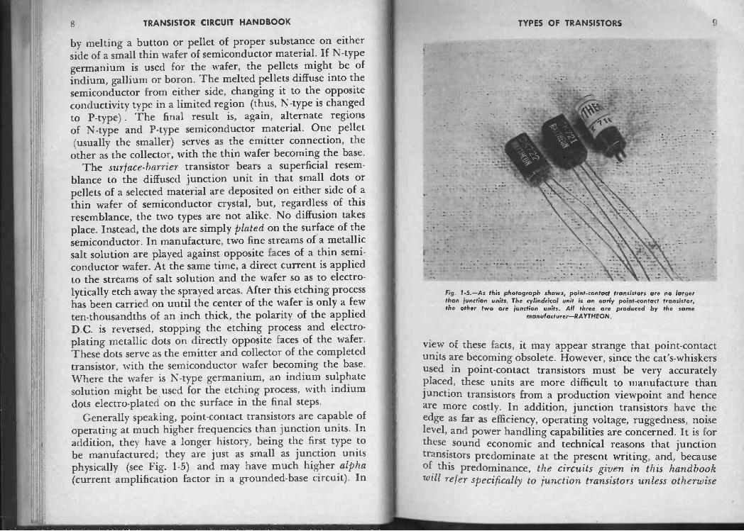
Today, transistors are available in a wide variety of stylesand types (see Fig. 1-1) , each with its own individual elec-trical characteristics. An even greater variety of types may beexpected in the future. Subminiature types are available forcompact wiring, larger types for power work. A hearing aidtransistor and a power unit are compared in Fig. 1-2. Sometransistors are designed primarily for switching and controloperations, others for audio work, and still others for highfrequency circuitry. Experimental transistors have been usedin R.F. circuits at frequencies as high as several hundredmegacycles. However, regardless of their individual electricalcharacteristics, all transistors may be classed in general group-ings based on (a) their type of construction, (b) number ofelectrodes, triodes, tetrodes, etc., and (c) the arrangement ofsemiconductors used. Let us discuss each grouping individu-ally.
Type of Construction: The four basic types of transistorconstruction currently employed are illustrated schematicallyin Fig. 1-3. Only triode transistors are shown in this illustra-

4 TRANSISTOR CIRCUIT HANDBOOK TYPES OF TRANSISTORS
Fig. 1-1.-A collection of typical transistors. A match book is includedfor size comparison. Transistors shown include units manufacured by RCA,GE, CBS-HYTRON, SYLVANIA, RAYTHEON, RADIO RECEPTOR, AMPEREX,
TRANSISTRON, and GERMANIUM PRODUCTS.
tion, with the emitter, base, and collector electrodes roughlyanalogous to the cathode, grid, and plate, respectively, of avacuum tube. Of the types shown, the point -contact transistoris the oldest, having made its first public appearance in 1948
at the Bell Telephone Laboratories in New York. The junc-tion transistor was not announced until three years later, inJuly of 1951. The surface -barrier transistor is the newest type,having, at this writing, just been released in commercialproduction quantities (1955) . All four types may be used incircuit work but the point -contact transistor appears to berapidly approaching obsolescence, for almost all major transis-tor manufacturers contacted by the author have indicated
Fig. 1-2.-A TRANSISTRON hearing aid type transistor compared to a SYLVANIApower ransistor to show relative sizes. Pencil gives an idea of true size.
that they have discontinued or are planning to discontinuethe production of point -contact units.
In construction, the point -contact transistor consists of aminute block of N -type or P -type semiconductor material,with two fine, closely spaced "cat's -whiskers" or point elec-trodes making pressure contact against its surface. The semi-conductor may be a small square measuring only 1/20 of aninch on each side by about 1/50 of an inch thick. The cat's -whiskers are separated by only a few thousandths of an inch.One electrode serves as the emitter and the other as the col-lector, with the small block of semiconductor material itselfserving as the base. The enlarged photograph of a point -contact transistor given in Fig. 1-4 clearly illustrates the type

6 TRANSISTOR CIRCUIT HANDBOOK TYPES OF TRANSISTORS
Emitter "Cat -Whiskers" Collectorv. -Point Contacts '44,
P Regions
Base
POINT -CONTACT TYPE
Emitter
N Type Material
Base
GROWN JUNCTION TRANSISTOR
Indium Pellets
P Regions
Emitter Collector
Base
DIFFUSED JUNCTION TRANSISTOR
Flat Etched OutRegion Plated Indium Dots
Emitter Collector
Base
SURFACE -BARRIER TRANSISTOR
Fig. 1-3.-The four types of transistor construction are shown schematicallyin this sketch.
of construction employed . . . both cat's -whiskers as well asthe small piece of semiconductor material are clearly visible.During the manufacturing process, small regions are formedunder each electrode's contact point with a conductivity typeopposite to that of the base. Where the base is N -type material,as in Fig. 1-3, these regions are given P -type properties, andvice -versa. The characteristics of the base material identifiesthe transistor. Thus, we have both N -base and P -base point -contact transistors.
Junction transistors may be manufactured in two ways-aseither grown or as diffused junction units. Both types areshown in Fig. 1-3. Their electrical characteristics are quitesimilar and they may be used in much the same circuits. Thegrown junction transistor is the more difficult to manufactureand consists of a single crystal of semiconductor materialhaving alternate layers of P -type and N -type substances. The
Fig. 1-4.-Enlarged photograph of a point -contact transistor. The two cat's -whiskers and the small block of semiconductor material are clearly visible.
central layer of the "sandwich" formed is much thinner thanthe outer layers and serves as the base. In practice this layermay have a thickness of only only one one -thousandths of aninch. To produce a grown junction crystal, certain impuritiesare added to a semiconductor, such as germanium, while it isin a molten state. These impurities are chosen so as to "dope"the material to give it either N -type or P -type characteristics.A large single crystal may then be grown by dipping a "seed"crystal into the molten metal and slowly withdrawing it underrotation. Additional impurities are added during the drawingprocess to produce alternate N -type and P -type layers in thesingle crystal. Later, the large crystal may be cut into smallersections and leads attached at the proper points to produceindividual transistors. A diffused junction transistor is made
8 TRANSISTOR CIRCUIT HANDBOOK TYPES OF TRANSISTORS 9
by melting a button or pellet of proper substance on eitherside of a small thin wafer of semiconductor material. If N -typegermanium is used for the wafer, the pellets might be ofindium, gallium or boron. The melted pellets diffuse into thesemiconductor from either side, changing it to the oppositeconductivity type in a limited region (thus, N -type is changedto P -type) . The final result is, again, alternate regionsof N -type and P -type semiconductor material. One pellet(usually the smaller) serves as the emitter connection, theother as the collector, with the thin wafer becoming the base.
The surface -barrier transistor bears a superficial resem-blance to the diffused junction unit in that small dots orpellets of a selected material are deposited on either side of athin wafer of semiconductor crystal, but, regardless of thisresemblance, the two types are not alike. No diffusion takesplace. Instead, the dots are simply plated on the surface of thesemiconductor. In manufacture, two fine streams of a metallicsalt solution are played against opposite faces of a thin semi-conductor wafer. At the same time, a direct current is appliedto the streams of salt solution and the wafer so as to electro-lytically etch away the sprayed areas. After this etching processhas been carried on until the center of the wafer is only a few
ten -thousandths of an inch thick, the polarity of the appliedD.C. is reversed, stopping the etching process and electro-
plating metallic dots on directly opposite faces of the wafer.These dots serve as the emitter and collector of the completedtransistor, with the semiconductor wafer becoming the base.Where the wafer is N -type germanium, an indium sulphatesolution might be used for the etching process, with indiumdots electro-plated on the surface in the final steps.
Generally speaking, point -contact transistors are capable ofoperating at much higher frequencies than junction units. Inaddition, they have a longer history, being the first type tobe manufactured; they are just as small as junction unitsphysically (see Fig. 1-5) and may have much higher alpha(current amplification factor in a grounded-base circuit). In
Fig. 1-5.-As this photograph shows, point -contact transistors are no largerthan junction units. The cylindrical unit is an early point -contact transistor,the other two are junction units. All three are produced by the some
manufacturer-RAYTHEON.
view of these facts, it may appear strange that point -contactunits are becoming obsolete. However, since the cat's -whiskersused in point -contact transistors must be very accuratelyplaced, these units are more difficult to manufacture thanjunction transistors from a production viewpoint and henceare more costly. In addition, junction transistors have theedge as far as efficiency, operating voltage, ruggedness, noiselevel, and power handling capabilities are concerned. It is forthese sound economic and technical reasons that junctiontransistors predominate at the present writing, and, becauseof this predominance, the circuits given in this handbookwill refer specifically to junction transistors unless otherwise

10 TRANSISTOR CIRCUIT HANDBOOK TYPES OF TRANSISTORS 11
stated. It is possible, of course, that modified point -contact tran-sistors will again be manufactured in production quantitiesin the future, perhaps for use in special purpose applications.
Number of Electrodes: The majority of present day transis-tors are triodes, although both point -contact and junctiontetrode units have been manufactured in moderate produc-tion quantities. Light sensitive phototransistors, in general,have only two electrodes, the third electrode being replacedby the light sensitive surface, and thus they may be consideredas a type of diode. A number of specialized transistors havebeen suggested as theoretical possibilities, and some have evenbeen hand -assembled for laboratory tests. Such units includethe analog transistor, PN "Hook" transistor, and variousmulti -purpose transistors. The analog transistor is a theoretical
type utilizing a special construction to obtain electrical char-acteristics similar to those obtained with vacuum tubes (i.e.,high input and high output impedances) . The PN "Hook"transistor is a special type junction transistor using threejunctions instead of the usual two (such as a PNPN transistor)and, theoretically, may have a gain many times greater thanthat obtained with conventional junction units. Multi -purposetransistors are roughly analogous to multi -purpose vacuumtubes, in which several relatively independent tube assembliesare contained within a single envelope, often with a commoncathode. As far as transistors are concerned, one possible typemight be a unit combining a PNP and a NPN junctiontransistor into a single unit, for application in push-pullstages using the complementary symmetry principle.
Arrangement of Semiconductors: As we have seen, mosttransistors are made up of alternate regions of N -type andP -type semiconductor materials. Even the point -contact trans-istor falls within this category, because small regions undereach electrode point are converted to a conductivity typeopposite that of the base material during the manufacturingprocess. The exact arrangement of semiconductor materialswithin the transistor determines the polarities of the D.C.
powersupply voltages applied to the electrode terminals when
the transistor is connected in a practical circuit. The applica-tion of incorrect voltages may very easily ruin the transistor.Hence it is extremely important that the worker be familiarwith the semiconductor arrangement in the transistors heemploys and, further, that he know the proper D.C. supplyvoltages for each basic transistor type.
Junction transistors are identified as PNP or NPN, withthe middle letter designating the conductivity characteristicof the base material. The schematic symbol employed issimilar for both types and consists of a heavy straight linerepresenting the base, together with slanting lines to the baserepresenting the emitter and collector terminals. An arrow-head identifies the emitter terminal. It points towards thebase in the case of PNP transistors, as shown at (a) in Fig. 1-6,and away from the base in the case of NPN units, as shown at(b) in Fig. 1-6. Proper power supply connections for bothtypes of transistors, connected as grounded -emitter amplifiers,are given in Fig. 1-6. Note that with the PNP transistor, boththe base and collector are negative with respect to the emitter.With the NPN unit, the base and collector are positive withrespect to the emitter.
Point -contact transistors are identified by the type of basematerial used in their construction rather than by the threeletter designation employed to identify junction units. Thus,we have both N -base and P -base point -contact transistors.However, as far as the schematic symbols and D.C. powersupply polarities are concerned, the N -base point -contacttransistor may be considered as equivalent to the PNPjunction transistor, while the P -base point -contact unit isequivalent to the NPN junction transistor.
CIRCUIT CONFIGURATIONSIn Fig. 1-6, the basic circuit arrangement for a grounded -
emitter transistor amplifier stage was used to illustrate thepower supply connections for PNP and NPN transistors.

12 TRANSISTOR CIRCUIT HANDBOOK CIRCUIT CONFIGURATION 13
Actually, there are three basic circuit arrangements that maybe employed, depending on the way a signal is applied to astage, the location of the output load impedance, and on howthe output is obtained from the stage. These are roughlyanalogous to the three basic vacuum tube amplifier circuits,with the grounded -emitter circuit approximately equivalent
In
PNP TRANSISTOR
(a)
Out
In
NPN TRANSISTOR
Base
(b)
Collector
Emitter
Fig. 1-6.-The schematic symbols and D.C. power supply connections for PNPand NPN transistors are shown here. The only difference in the schematicsymbols is in the direction in which the arrowhead points on the line
representing the emitter electrode.
Out
to the grounded cathode tube circuit, the grounded -base tothe grounded -grid, and the grounded -collector to the groundedplate or cathode follower. All three circuits are shown inFig. 1-7, together with the corresponding vacuum tube circuitarrangements. In each case, the power supply connectionsare for PNP junction transistors. With NPN units, supplypolarities would be reversed. Each stage is identified by thetransistor element (or tube electrode) that is common toboth the input and output circuits. This is generally calledeither the "grounded" or the "common" element but, in
actual practice, this element need not necessarily be connectedto circuit ground.
Referring to Fig. 1-7, with the grounded -emitter circuitarrangement (a) , the input signal is applied between the baseand emitter, with the output signal appearing between col-lector and emitter. The emitter is thus common to bothcircuits. In the grounded -base circuit (b) , the input signal isapplied between emitter and base, with the output appearing
CollectoOut
In
in Emitter CollectorOut
In
Emitter
RL
Grounded -EmitterTransistor Circuit ,
I.
Grounded Bose -Transistor Circuit
Cathode
R,
Grounded -Grid+
Tube Circuit(b)
Plato
Grid
Collector
GroundedCollector _Transistor Circuit
-
In
Grounded Plate TubeCircuitcp(Cathode Fo
lower)(c)
Fig. 1-7.-The three basic transistor circuit configurations with the roughlyequivalent vacuum tube circuit arrangements. Power supply polarities shownare for PNP transistors . . . polarities would be reversed for NPN units. See
TABLE A for a comparison of their basic electrical characterisics.
between collector and base, and the base is common to boththe input and output circuits. Finally, with the grounded -collector cricuit (c) , the input is applied between base andcollector and the output appears between emitter and col-lector, with the collector becoming the common element.Signal phase reversal occurs in the grounded -emitter, but notin the grounded -base and grounded -collector configurations.A single battery may be used to supply all D.C. operatingvoltages or a separate "bias" battery may be provided in thebase circuit, at the option of the individual designer. Two

14 TRANSISTOR CIRCUIT HANDBOOK
batteries are shown at (a) , a single battery at (c) . The basiccharacteristics of the three standard transistor circuit con-figurations are summarized in Table A. The characteristicslisted are based on currently available transistor types.
PART I - LABORATORY PRACTICE
Chapter 2
TECHNIQUES
Experimental transistor circuit work may be undertakenwith many of the same tools, laboratory test instruments andmechanical skills that are used in the assembly and test ofconventional vacuum tube circuits. Except where fundamentalsemiconductor research is involved, the individual or labo-ratory contemplating transistor circuit experiments need notanticipate more than a modest expenditure for special toolsor laboratory equipment, nor need the worker have to spenda long training period to acquire new skills or to learn newtechniques. In most cases, any special skills that are neededmay be acquired on the job, simply by approaching earlyprojects with care and forethought, following the advice givenin an old proverb . . . "to make haste slowly!"
Perhaps the most important practical skill the laboratorytechnician or home experimenter need acquire is the abilityto work with components many times smaller than those usedin conventional electronics work. There is no question thatsomewhat greater skill, and certainly greater patience, isrequired when working with subminiature components thanwhen working with `full-sized" parts. In addition to sharpen-ing his mechanical skills, if the technician has worked withvacuum tube circuits exclusively for a long period of time,he may have to rechannel his thinking somewhat so that hecan readily accept and work with voltage, current and im-pedance values of a different order than those with which hemay have been familiar. When working with vacuum tubecircuits, for example, D.C. operating voltages in the neighbor-hood of several hundred volts are the rule-but with transis-tors, high voltages are seldom used, even in higher power
15

16 TRANSISTOR CIRCUIT HANDBOOKTOOLS AND LABORATORY EQUIPMENT i7
circuits. Supplies of a fraction of a volt may be encounteredin some circuits. Then, too, when dealing with the usualtransistor circuits, he will have to pay close attention to powersupply polarities . . . reversed plate voltage may seldomdamage a vacuum tube, but reversed D.C. supply voltage isalmost sure to ruin a transistor. To complicate matters, dif-ferent types of transistors may require exactly opposite supplyvoltage polarities (i.e., PNP and NPN units) , and, in somecases, both types may be used in the same circuit (i.e., com-plementary symmetry push-pull amplifiers) . In using transis-tors for the first time, the worker will be faced with theseeming paradox of working with components that aresimultaneously more rugged mechanically, yet more easilydamaged electrically than vacuum tubes.
TOOLS AND LABORATORY EQUIPMENTTransistor circuits may be wired into either "full-sized" or
subminiature equipment. But even if no special attempt ismade at subminiaturization, since transistors and most transis-tor components are much smaller than conventional electroniccomponents, they are a little awkward to handle with full-sizedhand tools. For this reason, the technician planning appre-ciable transistor circuitry work should be outfitted withscaled -down tools. Jeweler's pliers are ideal for this type ofwork and are now stocked by many Electronic Parts Distribu-tors. A typical assortment of hand tools especially selectedfor transistor circuit work is shown in Fig. 2-1. Included area cased set of jeweler's pliers, an OR YX subminiature solder-ing instrument, a scribe, tweezers, small brush, pocket magni-fier, and a set of jeweler's screw -drivers. The small screw-drivers are not essential to wiring, of course, but are usefulwhen working with the miniature assemblies in which transis-tors are frequently installed. Additional tools which would beuseful in subminiature assembly work, but which are notshown in the photograph, would include a small hand orbench vise, fitted with smooth soft -metal jaws, a penlight,
Fig. 2-1.-Hand tools useful when working with transistor circuits.
miniature socket wrenches, a set of Swiss Needle Files, and apower tool kit, including the power unit, small drill bits,rotary brushes, and similar accessories.
Techniques: Although the majority of small tools are han-dled and used in the same way their conventional sizedcounterparts are employed, there are a few special techniqueswhich the worker may wish to learn. The use of a jeweler'sscrewdriver is illustrated in Fig. 2-2. The cap on the screw-driver's handle is free to rotate and is held lightly with onefinger, which both applies pressure and guides the tool. Thebody of the handle is rotated gently by the thumb and anotherfinger. This technique makes it difficult to apply excessivetorque, thus minimizing the danger of damage to the screw-driver's blade or any tendency to "strip" the threads of small

18 TRANSISTOR CIRCUIT HANDBOOK TOOLS AND LABORATORY EQUIPMENT 19
Fig. 2-2.-Proper technique for using a jeweler's screwdriver.
machine screws. When wiring transistorized circuits, a smallpencil -type soldering instrument is preferable to a full-sizedtool. The tip should be kept clean and well -tinned so allsoldering operations may be completed as quickly as practi-
cable. The use of a heat sink is recommended (see section onCARE OF TRANSISTORS and Fig. 2-9) . In subminiaturewiring, simple lap joints are frequently employed in prefer-ance to the "wrap -around" connections common in conven-tional electronic assemblies. In some instances, the worker
may find it easier to clamp his soldering instrument in a vise,holding the components to be wired in his hands, as shownin Fig. 2-3. While resistors and small capacitors may be held
Fig. 2-3.-Some technicians prefer to clamp their soldering instrument in a vise.
in place by their leads, transformers and other large com-ponents are frequently mounted either by cementing in placeor by clamping in position with small spring or wire clips.Other special assembly techniques employed in transistor

20 TRANSISTOR CIRCUIT HANDBOOK TOOLS AND LABORATORY EQUIPMENT 21
circuit work include the use of etched or printed circuits andthe potting of sub -assemblies in plastic. These special topicswill be discussed in Part IV of this volume.
Test Equipment: Audio and R.F. Signal Generators, Oscillo-scopes, VTVMs, Impedance Bridges, in fact, almost every typeof electronic test equipment found useful in vacuum tubecircuit work will find similar applications in experimentaltransistor work. Some test equipment items are especiallyimportant. A good assortment of individual meters is highlydesirable and, for circuit development work, almost manda-
tory. If voltmeters are sometimes considered a shade morevaluable than current meters in vacuum tube work, withtransistors the reverse is true. Thus, while the meter assort-ment should include several D.C. microammeters for check-ing base current values and milliammeters for collector andemitter current measurements (or, in the case of high powertransistors, D.C. ammeters) , one or two D.C. voltmetersshould be ample for general work, especially if multi -rangeinstruments are provided. Since battery power supplies areused extensively in transistor circuitry, a good Battery Testerwould be a desirable addition to the lab. The tester chosenshould be designed to check the batteries under load condi-tions. If precise circuit tests and transistor parameter measure-ments are to be made, one or more adjustable output ConstantCurrent power supplies are desirable. However, for generalexperimental work, any standard adjustable voltage D.C.
supply will be found almost as useful, provided its outputcan be reduced to near zero and that low voltages can beobtained without difficulty. Where circuit development is
undertaken with a view towards eventual mass production,enviromental test chambers are a desirable addition to the
laboratory's complement of test equipment, to permit thethorough checking of compensation circuits under actualconditions. At this writing, commercially available transistorsare somewhat more sensitive to temperature and humidityvariations than are vacuum tubes and a thorough enviro-
mental test of circuits contemplated for production is goodengineering practice.
Breadboarding: It is standard engineering practice to bread-board or to "rough assemble" new circuits, not only as adouble-check on the validity of a theoretical design, but alsofor determining circuit values that are difficult either tocalculate or to estimate in advance. Breadboarding may beused for checking mechanical and electrical layouts and forlocating unforeseen "bugs" in a design. In addition, a bread-board assembly, once checked out, is useful for determiningthe practical effect of component tolerances on circuit opera-tion. Many experienced practical electronics engineers preferto work up a new circuit design right on a breadboard chassis,keeping mathematical calculations and other paper work to a
Fig. 2-4.-A "Universal" Breadboard chassis designed for ransistor tests.

22 TRANSISTOR CIRCUIT HANDBOOK
minimum. With transistors, the breadboard check of a circuitdesign is, if anything, more important than with vacuum tubecircuits. Unfortunately, the small physical size of transistorsmakes them a little difficult to handle conveniently on the lab.bench. For this reason, the individual laboratory worker mayfind it worthwhile to assemble a "breadboard" chassis specifi-
F:g. 2 -5. --Detail of transistor socket mounting.
cally for checking transistor circuits. One such "universalbreadboard" chassis is shown in Fig. 2-4. A subminiaturein -line tube socket serves as a transistor socket, and is mountedon three small stand-off terminals. A detail view of the socketmounting is given in Fig. 2-5. Several terminal strips areprovided on the chassis to permit the easy mounting andwiring of resistors, capacitors, and other components. The use
TOOLS AND LABORATORY EQUIPMENT 23
of a breadboard chassis is illustrated in the typical lab. bench
set-up shown in Fig. 2-6. For maximum utility, the basicchassis is used in conjunction with clip type test leads andpanel meters. In addition to home built chassis, commercial"breadboards" are available-see Part IV. Other useful acces-sories, not shown in the photograph, would include Resistance
Fig. 2-6.-A ypical experimental set-up for checking a breadboardedtransistor circuit.
and Capacitor Substitution Boxes, and an assortment of small"universal" transformers and inductors. Proper electrode pinconnections for a standard triode transistor are shown at (a)in Fig. 2-7, for a tetrode junction transistor at (b) in the sameillustration. However, not all manufacturers adhere to thisstandard" pin arrangement. Pin connections for certain
transistors of three popular manufacturers are shown at (a) ,

24 TRANSISTOR CIRCUIT HANDBOOK
(b) , and (c) of Fig. 2-8. The pin arrangement shown at (a)is used on TRANSITRON subminiature types 2N88, 2N89and 2N90. The connections shown at (b) are employed byPHILCO on their types 2N47, 2N49 and SB-100. And thepin arrangement used by RAYTHEON on their types CK721,CK722, CK725 and CK727 is shown at (c) .
Note Wide Spacing
(a) (b)Fig. 2-7.-Pin connections for standard triode (a) and tetrode junction (b) transistors.
Base
Red dot
Collector Emitter
(0)
Red Ime
,Red lineEmitter
Th;":".CollectorBase
(b)
Emitter
E
e- Red dot
Base
Red dot
Collector
(c)
Fig. 2-8.-Special transistor pin connections used by some manufacturers.TRANSITRON (a); PHILCO (b); RAYTHEON (c).
CARE OF TRANSISTORS 25
CARE OF TRANSISTORS
It is unlikely that transistors will ever be "given away" in
quantities, and therefore, regardless of how inexpensive theymay become, they still represent a financial investment,whether their cost is borne by the Research Account of alarge corporation or the "hobby budget" of a home experi-menter. And any investment should be handled with care. Ithas been mentioned that transistors are many times morerugged than vacuum tubes as far as mechanical shock isconcerned. Some transistors may successfully withstand anacceleration of 20,000 to 30,000 g,* whereas an accelerationof 750 g is about the upper limit as far as vacuum tubes areconcerned. But this inherent ruggedness is no excuse for de-liberate abuse. Although mechanically rugged, transistors maybe easily damaged by electrical overload or excessive heat.Therefore, the laboratory worker will find it profitable toadopt a few "rules of practice" to follow when working withtransistors. Later, as he gains experience, he will find himselffollowing these rules almost subconsciously. For ease in refer-ence, the basic rules are listed below in numerical order . . .
but remember that the order of listing does not indicate theorder of importance-all are equally important.
1. Avoid Excessive Heat - High temperatures, whetherapplied externally or internally generated, may cause perma-nent damage to a transistor or permanent change in itselectrical characteristics. Excessive heat may be avoided bytaking care in soldering (see comments under WIRINGTECHNIQUES, as given below) , by avoiding operationclose to hot vacuum tubes, power resistors or other com-ponents likely to dissipate quantities of heat, and by avoidingoperation at near maximum ratings under conditions of highambient temperatures. When transistors are used at higherthan normal temperatures, their operational specs should be"derated" accordingly . . . refer to the manufacturer'sspecification sheets for specific suggestions.
g -=Acceleration due to gravity; the standard unit for measuring acceleration; equal to32 ft /sec.

26 TRANSISTOR CIRCUIT HANDBOOK CARE OF TRANSISTORS 27
2. Avoid Electrical Transients - Voltage or current surgeswhich exceed the transistor's maximum ratings, even if onlymomentarily, may cause permanent damage. When workingwith new transistor circuit designs, transient pulses may beminimized by avoiding the sudden application of supplyvoltages-use a variable supply and adjust slowly to finalvalues. Avoid the use of circuits which involve extensiveswitching of high level signals or D.C. voltages. When workingwith assembled circuits or built-up equipment, do not insertor remove transistors from their sockets with the power ON
unless absolutely necessary.3. Always Double -Check Transistor Type and Voltage
Polarities - Remember that different types of transistors re-quire different D.C. supply voltage polarities for operation,and that the application of an incorrect voltage may damagethe transistor. Before wiring a circuit, make sure you knowwhether the transistor is a PNP or NPN unit (or a P -baseor N -base type, if it is a point -contact transistor) , and checkto see that all supply voltages are applied with the properpolarity.
4. Observe the Maximum Ratings - Although some elec-tronic components are conservatively rated and may beslightly overloaded without damage, the Absolute MaximumRatings specified by transistor manufacturers mean exactlythat. Even a momentary overload may cause irreparable dam-age. When breadboarding or testing new circuits, it is a goodidea to connect D.C. current meters in series with eachelectrode to maintain a constant check on emitter, collectorand base currents. The meters should be by-passed with ap-propriate capacitors when working with A.C. amplifiers,oscillators, and similar circuits, of course.
WIRING TECHNIQUES: In order to avoid possible heatdamage, all transistor circuit wiring should be carried out asquickly as possible, using a hot, clean, well -tinned solderinginstrument. Do not solder to transistor socket terminals with-out first removing the transistor, and allow ample time for
Fig. 2-9.-Proper use of a heat sink in soldering a transistor lead.
the joints to cool before reinserting the transistor. Where atransistor is wired directly into a circuit by means of its leads,use the maximum lead length consistent with good electricallayout and circuit design, protecting the bare wire withspaghetti tubing. For maximum protection, use a heat sinkon the transistor lead between the soldered joint and the bodyof the transistor itself. The proper use of a heat sink is clearlyillustrated in Fig. 2-9. The transistor lead being soldered isgrasped with a pair of long -nosed pliers, which act to conductheat away from the transistor proper. When installing surface -barrier transistors, care should be taken to avoid voltagesurges derived from soldering irons operating from A.C. lines.As a precaution against such surges, the use of gun -type sol-dering instruments or isolation transformers is recommended.
POWER TRANSISTORS: High -power transistors present spe-cial problems in practical circuit work. First, because they

28 TRANSISTOR CIRCUIT HANDBOOK CARE OF TRANSISTORS 29
are designed to handle watts instead of milliwatts, they gen-erate a good deal of internal heat. Most commercial powertransistors are designed to dissipate as much of this heat aspossible. Two techniques are used. One is to design theexternal case to act as a heat radiator by providing coolingfins. Another is to make provision for mounting the transistordirectly to a metal chassis, which then acts as an external heatsink. Often, both techniques are used at the same time, asshown in Fig. 2-10. Another problem encountered with high -power units, especially with germanium transistors, is thatof "runaway." This generally occurs at high ambient tempera-tures when the internal power dissipation through self -heatinglowers the resistance of the semiconductor, materially increas-ing collector current, thereby increasing power dissipation
Fig. 2-10.-High-power transistor mounted on a chassis for maximum heat dissipation.
and raising the temperature still further. This can lead, even-tually, to serious damage, if not complete destruction, of thetransistor. Even if the transistor itself is not seriously damaged,the circuit becomes unstable. To guard against the possibilityof collector current runaway, stabilization of D.C. operatingpoints is strongly recommended in all applications involvingthe use of high -power transistors.
TESTING TRANSISTORSThe practical laboratory worker has several testing tech-
niques at his disposal. First, he can use a laboratory-type Tran-sistor Test Set. These instruments are currently produced bya number of manufacturers and, for the most part, incorporatefacilities for completely evaluating all important character-istics and parameters of both point -contact and junction tran-sistors. Transistor Testers are discussed in Part IV.
If the worker does not have a commercial Transistor TestSet available, he can duplicate most of the tests by usingindividual instruments. The basic instruments needed formost tests include a high -impedance VTVM, individual cur-rent meters and at least two adjustable output constant -current D.C. power supplies-one for each transistor electrodein the standard configurations. Where an especially builtconstant -current supply is not available, a satisfactory substi-tute may be assembled by connecting a high value resistor inseries with a conventional adjustable B voltage supply. Forbest results the series resistor should have a value at least 100(and preferably 1000) times higher than the expected load-this means the D.C. output current will be virtually inde-pendent of load and the assembly will act like a true constant -current supply. The expected load may be determined byreferring to the manufacturer's specification sheet for thetransistor to be tested; the load is the D.C. resistance of theelectrode in question. Referring to the data sheet on thetransistor, the equipment is set up to supply specified currentsto the various electrodes and the D.C. electrode voltages are
30 TRANSISTOR CIRCUIT HANDBOOK TESTING TRANSISTORS 31
measured using the VTVM. These are actual electrode volt-ages . . . not source voltages, for a considerable drop willoccur across the series resistor. A series of tests may then bemade, with one electrode current kept constant and the otherelectrode current varied in small steps. These measured valuesmay be plotted on a graph and compared to the characteristiccurves given in the transistor manufacturer's data sheet. Es-sentially the same technique is employed to make tests ofboth grounded -base and grounded -emitter circuits, and toobtain data to plot such curves as emitter current vs, emittervoltage for a constant collector current (grounded base con-figuration) , collector current vs, collector voltage for a con-stant emitter current (grounded base) , collector current vs.collector voltage for a constant base current (grounded emit-ter) , etc. When making tests of this nature, all the precautionsmentioned in the section CARE OF TRANSISTORS shouldbe observed.
Detailed tests of transistor characteristics, as important asthey may be in a complete over-all evaluation of the compo-nent, are much too time consuming for most types of practicalcircuit work. A simpler and much more rapid test may bemade by setting up a basic amplifier stage, applying a knowninput signal and proper D.C. operating voltages to the transis-tor, then checking over-all gain and individual electrode cur-rents. While such a test does not give a quantitative evaluationof the transistor, it does give a qualitative "Good -Bad" check.If the gain is unusually low, or if the various electrode currentsrun high, or both, the transistor may be considered defective.This test is more effective in those cases where the transistormanufacturer has supplied "Typical Operating Character-istics" as part of his specification sheet, for the measured valuesmay be compared directly to known standards. However,when making such a comparison, a one-to-one correspondenceshould not be expected, for all transistors are manufacturedwithin broad tolerance limits . . . only where the measuredvalues are far different from expected values should the tran-
sistor be considered defective. The "Typical Operating Char-acteristics" may also be used as a guide in setting up the orig-inal test circuit.
Where a transistor is to be used in a fairly critical circuit,such as a high -gain, low noise audio amplifier, or as a highfrequency R.F. oscillator, there is no really satisfactory testother than that of substitution. That is, the suspected transis-tor is actually tried in the desired circuit. If it fails to givesatisfactory performance, it is considered "Bad," at least asfar as the one circuit is concerned. Of course, transistors failingthis test may still be satisfactory for other, less critical, appli-cations. A modification of this test technique, sometimes usedby manufacturers of transistorized equipment, is to set up atest circuit which electrically duplicates the equipment beingproduced. All transistors are first checked in the test circuitand individually selected for best performance in variousstages of the equipment. As an example, in the manufactureof a transistorized superheterodyne receiver, some units may beselected to give their best performance as local oscillators,others as I.F. amplifiers, and still others as detectors andaudio amplifiers.
CIRCUIT MODIFICATIONSAlthough all the circuits given in this volume have been
"bench -tested" in the laboratory, economic considerationshave prohibited their production engineering. It is to beexpected, therefore, that the individual experimenter whoassembles the circuits may, in some instances, find it necessaryto make minor changes in component values when workingwith transistors or other components having characteristicsdifferent from those used by the author, even if due only tonormal tolerance variations. In addition, since any circuitdesign generally represents a compromise between different,often conflicting, situations, if the individual builder or ex-perimenter wishes his circuit to excell in one special character-istic, such as having maximum battery life, maximum gain,

32 TRANSISTOR CIRCUIT HANDBOOK
minimum distortion, minimum noise, maximum selectivity,or maximum power output, he will find it necessary to makeexperimental changes in the circuit to emphasize the desiredcharacteristic. In some cases, the change may be little morethan the adjustment of one or two component values. In othercases, considerable modification of the basic circuit may benecessary. Unless otherwise indicated, special temperatureand humidity compensation or D.C. stabilization circuits havenot been included as part of the experimental circuits shown,for the use of such circuits is largely a matter of individualneed and, therefore, is best left to the individual designer.
Several general rules should be followed when makingexperimental circuit modifications. First, of course, the workershould adhere to all the suggestions given in the sectionCARE OF TRANSISTORS. In most circuits, NPN junctiontransistors may be substituted for PNP units with corres-ponding characteristics, provided power supply polarities arereversed. Before changing components or connections in anytransistor circuit, the experimenter will find it desirable toconnect D.C. current meters in series with the various transis-tor electrode leads, so that he can monitor changes in currentvalues at all times, making sure that no circuit or componentchange permits the maximum ratings of the transistor to beexceeded. For additional information of value in modifyingand re -designing circuits, the reader will find it worthwhile torefer to the general Reference Data given in Part IV of thisvolume and especially to the reference sources listed in theBibliography.
PART I - LABORATORY PRACTICE
Chapter 3
COMPONENTS
Many of the electronic and hardware components used intransistor circuitry are simply scaled -down versions of con-ventional parts. This is not too surprising, for these semi-conductor amplifiers almost naturally call for subminiaturecomponents to match their own minute physical size. But themere desirability and need for subminiature components isnot, in itself, enough to insure their design and production.They must be feasible as well, both from an economic and aproduction engineering viewpoint. Fortunately, the uniqueelectrical characteristics of transistors almost ideally fit themfor the design of subminiature components.
It is an established fact that the physical size of electroniccomponents is dependent, to a large extent, upon their powerhandling capacity and voltage breakdown characteristics. Ahigh -capacity, high -voltage capacitor must be large physicallybecause a comparatively thick dielectric is needed to with-stand high voltage stresses and the thick dielectric, in turn,reduces capacity, necessitating a larger unit to obtain highcapacity. A high wattage resistor must be large to obtainsufficient surface area to dissipate a quantity of heat. And,similarly, high power transformers are large because heavierconductors are required to carry large currents, thicker insula-tion is needed to withstand high voltages, and more iron isneeded in the core to handle the strong magnetic fieldsproduced without reaching saturation. With the majority oftransistor circuits, powers are measured in the milliwatts andcurrents in the micro- and milliamperes; operating voltagesare low-but a fraction of those found in vacuum tube circuits.Hence, the subminiaturization of components designed spe-
33

34 TRANSISTOR CIRCUIT HANDBOOK
cifically for transistor circuitry is not only desirable, buteconomically feasible as well-and such subminiaturizationmay be considered good engineering practice.
RESISTORS AND CONTROLS: Several subminiature resistors,a volume control and a selector switch well suited to transistorcircuitry are shown in Fig. 3-1. A transistor and a package ofbookmatches are included for size comparison purposes. Thetransistor is a GE PNP junction triode, the resistors aremanufactured by FORTIPHONE, LTD. of England, thevolume control is a CENTRALAB item and the selectorswitch is a standard GRAYHILL unit. Subminiature resistorsand controls, like a number of other subminiature compo-nents, were manufactured commercially long before transis-tors became practical commercial items. Prior to the practical
Fig. 3-1.-Subminiature resistors, volume control, and selector switch.Transistor and bookmatches included for size comparison.
CIRCUIT MODIFICATIONS 35
development of the transistor, such components were usedprincipally in vacuum tube hearing aids, in miniature instru-ments, and in specialized types of military equipment. Ingeneral, except for their physical size and minor refinementsin construction, subminiature resistors are similar to theirlarger counterparts.
CAPACITORS: The low input impedance of the averagetransistor amplifier stage necessitates the use of fairly largeinterstage coupling capacitors in R -C and impedance -coupledtransistor audio amplifiers. In the past, large capacity andsmall size were not considered compatible features, but withthe development and successful commercial production oflow voltage aluminum and tantalum electrolytic capacitors,it is now possible to obtain fairly large capacities in units
Fig. 3-2.-Subminiature electrolytic capacitors compared to a standard paper unit.

36 TRANSISTOR CIRCUIT HANDBOOK COMPONENTS 37
which, in some ratings, are smaller, physically, than thetransistors with which they are used.
A typical assortment of subminiature capacitors is illus-trated in Fig. 3-2, with a GE PNP triode transistor and anormal -sized paper capacitor included for size comparisonpurposes. The large capacitor shown is a standard 0.25 Mfd.,600 volt paper capacitor manufactured by GUDEMAN. Onealuminum and two small tantalum capacitors are shown; allthree are rated at 2.0 mfd. or more, with working voltagesfrom 6 to 18 volts. Three manufacturers are represented-BARCO, MALLORY, and GE. Also shown is a miniaturemetallized paper capacitor, made by AEROVOX. Althoughrated at 0.5 Mfd., 200 volts, the unit is considerably smallerthan the standard paper tubular item. In spite of their largersize, miniature metallized paper capacitors are sometimesused in transistor circuits in place of electrolytics wherespecial characteristics are needed for critical applications.
Some idea of the comparative sizes of commercially availa-ble capacitors may be obtained by comparing their relativevolumes in terms of units having the same capacity and work-ing voltage. Taking a 1Mfd., 150 volt foil -type capacitor asthe "standard," if a paper unit has a volume of 100%, ametallized paper unit will have a volume of 40%, an alumi-num electrolytic a volume of 15%, and a tantalum electrolytica volume of 10%. Of course, low working voltages are therule rather than the exception in transistor circuitry, and, inlow voltages, the size differential between the different ca-pacitor types is even greater.
Application -wise, aluminum electrolytics are less costlythan tantalum units, but the tantalum units have the edge asfar as life and temperature characteristics are concerned.Tantalum electrolytic capacitors are manufactured in twoforms. One employs the conventional foil construction and ismade by winding two paper -separated foil electrodes into acylindrical unit. The electrolyte is held by the absorbentpaper. During the manufacturing process, an oxide film is
formed on the foil, and this serves as the dielectric, just as ina conventional electrolytic capacitor. Non -polarized designsare possible if both foils are filmed with oxide. The otherform employs an electrode of sintered powdered tantalum.The anode is made by compressing the powdered tantaluminto the proper shape, then welding the particles together bysintering in a vacuum furnance. The final result is a veryporous mass which has a large surface area for dielectric oxideformation. In the foil type of construction, the outer caseserves simply to contain the wound foil capacitor, but in thesintered anode type, the case, generally made of silver, servesas the cathode.
In transistorized R.F. circuits, small paper as well as bothceramic and silver mica capacitors are employed. Variablecapacitors may be compression trimmers, conventional rotat-ing air dielectric units, or a newly introduced type whichemploys a teflon dielectric. Other types are in a developmentalstage and may be available in the near future.
R.F. COILS AND TRANSFORMERS: The subminiaturizationof R.F. coils presents special problems to the design engineer.As coils are made smaller, finer wire must be used in theirconstruction, increasing both D.C. and A.C. resistances. Inaddition, more compact construction generally means higherdistributed capacities and greater losses. All of these factorstend to reduce coil "Q" and efficiency, both at high fre-quencies where distributed capacities are important and atlow frequencies which require larger inductance values. Asif these problems were not discouraging enough to the de-signer, the transistors with which the coils and transformersare used offer a low impedance loading, coupled with fairlyhigh internal capacities . . . additional factors to reduceover-all circuit "Q." Nonetheless, R.F. coil manufacturershave been able to design successfully and to produce inproduction quantities R.F. coils and transformer suitable forsubminiature transistor circuitry.
A selection of commercially available coils is shown in Fig.

38 TRANSISTOR CIRCUIT HANDBOOK
3-3, together with a RAYTHEON type CK722 PNP junctiontransistor and a package of bookmatches for size comparisonpurposes. Included are two shielded I.F. transformers and alocal oscillator coil for a broadcast band superheterodyne re-ceiver. One of the I.F. transformers is manufactured by
Fig. 3-3.-Subminiature R.F. coils and If. transformers.
AUTOMATIC MANUFACTURING CORPORATION,the other I.F. transformer and the oscillator coil are productsof the VOKAR CORPORATION. In all three units, pow-dered iron cores are used, both for tuning and to help main-tain good stability and a reasonably good "Q" in a smallvolume coil. As an example of the specifications encounteredin this work, the smaller I.F. transformer (VOKAR) ispermeability tuned, incorporates a 200 Mmf. capacitor withinits shielding case, and is designed to resonate at 262 Kc with
COMPONENTS 39
an unloaded "Q" of not less than 80. The mechanical designis such as to permit installation on a printed circuit wiringboard, with final connections accomplished through a dipsoldering process.
AUDIO COILS AND TRANSFORMERS: The size of the copperwire used in the winding and the amount of iron in the corelaminations of an audio transformer are both dependent onthe direct current which flows through the winding as wellas on the power handled by the unit. The amount and typeof insulation required between individual windings andbetween the winding and core depends on the voltagesapplied to and developed within the transformer. All threefactors . . . core size, winding, and insulation . . . affect theover-all size of the transformer. Except for special "high -power" applications, in the majority of transistor audio cir-cuits D.C. currents are small, on the order of one or twomilliamperes; D.C. voltages are low, from 1.5 to 12 volts orso; and, of course, powers are small, perhaps from a fractionof a milliwatt up to 20 or 30 milliwatts. In the "high -power"circuits, D.C. voltages may run from 6 to 60 volts, or more,and currents from 100 Ma. up to several amperes. How-ever, in the low power circuits, subminiaturization of audioinput, coupling and output transformers is both feasible anddesirable.
Several typical miniature iron -core audio transformers areshown in Fig. 3-4, together with a GE PNP junction transistorand a package of bookmatches. The largest unit shown is anEnglish -made audio choke, designed primarily for hearing aidapplications. The remainder are American -made audio trans-formers. The two middle units are, respectively, a "Sub-Ouncer" and a "Sub-subouncer," both manufactured byUTC. The smallest transformer shown is not appreciablylarger than the transistor itself and is one of a series of thesmallest iron -core transformers currently manufactured forcommercial use. Some of these units weigh only about 1/10of an ounce. They are manufactured by the CHICAGO

40 TRANSISTOR CIRCUIT HANDBOOK
Fig. 3-4.-Subminiature iron -core audio transformers and choke.
STANDARD TRANSFORMER CORPORATION. Not-withstanding their small size, they are quite well made andhave a frequency response more than adequate for theirintended applications.
AUDIO TRANSDUCERS: Hearing aids and other types ofaudio amplifiers require some kind of electromechanicaltransducer to convert acoustic energy into electrical signalsand vice versa. When dealing with transistorized circuits, itis often desirable to use audio transducers which are com-parable in physical size to the transistors and their relatedsubminiature electrical components. A selection of typicalunits especially designed for transistor circuitry is shown inFig. 3-5 along with a SYLVANIA transistor. Again, a packageof bookmatches is included for size comparison purposes.The loudspeaker is a miniature, high -efficiency PM unit
COMPONENTS
Fig. 3-5.-Subminiature audio transducers . . . loudspeaker, microphone,and earphone. Bookmatches and transistor give some idea of relative sizes.
designed and manufactured by the JENSEN MANUFAC-TURING CO. of Chicago, Illinois. Measuring only 11/8"deep by 234" in diameter, the unit weighs less than 23/4ounces, yet has a power rating of 150 milliwatts and a usefulfrequency range from 250 to 3000 cps. In the center of thephotograph, next to the transistor, is a SHURE BROTHERSmagnetic microphone cartridge. With good sensitivity andan output impedance of only 1000 ohms, this unit providesan excellent match directly to the input of a junction transis-tor connected as a grounded -emitter amplifier. Also shownin the illustration is a magnetic hearing aid type earphone,together with its matching miniature cord. Manufactured byFORTIPHONE, LTD. of England, this item is available ina number of impedance values to meet almost any desired
42 TRANSISTOR CIRCUIT HANDBOOK COMPONENTS 43
output circuit. In most cases, hearing aid earphones are usedin conjunction with a plastic earpiece custom molded to fitthe individual user. Because of the comparatively low im-pedances encountered in transistor circuits, electromagnetictransducers are used to a greater extent than piezoelectricunits, as demonstrated by the sample units described.
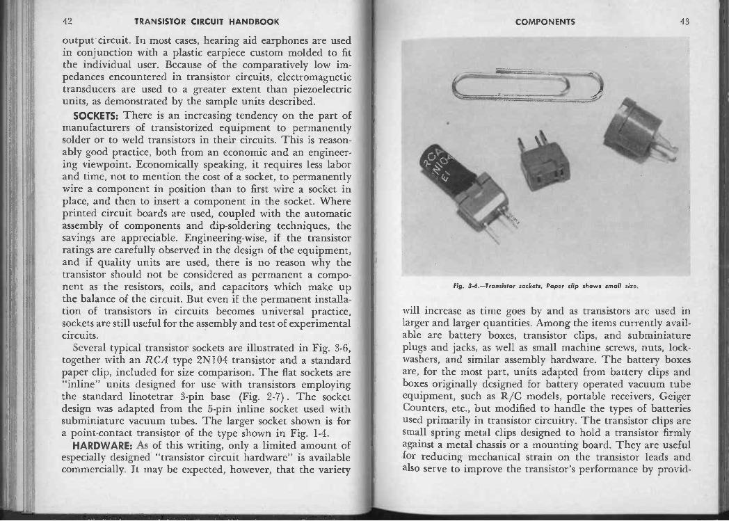
SOCKETS: There is an increasing tendency on the part ofmanufacturers of transistorized equipment to permanentlysolder or to weld transistors in their circuits. This is reason-ably good practice, both from an economic and an engineer-ing viewpoint. Economically speaking, it requires less laborand time, not to mention the cost of a socket, to permanentlywire a component in position than to first wire a socket inplace, and then to insert a component in the socket. Whereprinted circuit boards are used, coupled with the automaticassembly of components and dip -soldering techniques, thesavings are appreciable. Engineering -wise, if the transistorratings are carefully observed in the design of the equipment,and if quality units are used, there is no reason why thetransistor should not be considered as permanent a compo-nent as the resistors, coils, and capacitors which make upthe balance of the circuit. But even if the permanent installa-tion of transistors in circuits becomes universal practice,sockets are still useful for the assembly and test of experimentalcircuits.
Several typical transistor sockets are illustrated in Fig. 3-6,together with an RCA type 2N104 transistor and a standardpaper clip, included for size comparison. The flat sockets are"inline" units designed for use with transistors employingthe standard linotetrar 3 -pin base (Fig. 2-7) . The socketdesign was adapted from the 5 -pin inline socket used withsubminiature vacuum tubes. The larger socket shown is fora point -contact transistor of the type shown in Fig. 1-4.
HARDWARE: As of this writing, only a limited amount ofespecially designed "transistor circuit hardware" is availablecommercially. It may be expected, however, that the variety
Fig. 3-6.-Transistor sockets. Paper clip shows small size.
will increase as time goes by and as transistors are used inlarger and larger quantities. Among the items currently avail-able are battery boxes, transistor clips, and subminiatureplugs and jacks, as well as small machine screws, nuts, lock -washers, and similar assembly hardware. The battery boxesare, for the most part, units adapted from battery clips andboxes originally designed for battery operated vacuum tubeequipment, such as R/C models, portable receivers, GeigerCounters, etc., but modified to handle the types of batteriesused primarily in transistor circuitry. The transistor clips aresmall spring metal clips designed to hold a transistor firmlyagainst a metal chassis or a mounting board. They are usefulfor reducing mechanical strain on the transistor leads andalso serve to improve the transistor's performance by provid-

44 TRANSISTOR CIRCUIT HANDBOOK COMPONENTS 15
ing a heat sink against the transistor's case which helpsconduct away internally generated heat.
POWER SUPPLIES: Since the operating voltages needed bytransistor circuits are low, with current requirements minute,both A.C. line -operated units and batteries are practical foruse as transistor power supplies. With the exception of special"high -power" transistor circuits, A.C. power supplies, whereused, are generally much simpler, more compact; and con-siderably lighter than their vacuum tube counterparts. R -Cfilter networks are practical because of the low currentsneeded and, therefore, are used extensively in place of themore costly L -C filters favored for vacuum tube powersupplies. Constant current power supplies are needed formeasuring transistor parameters and for other laboratory testsand, theoretically at least, should always be used for biascurrent purposes in transistor circuits. Nonetheless, in actualpractice more conventional power supplies are generally em-ployed, with a large value series resistor serving to limitcurrent flow and to give the practical effect of a constantcurrent supply. Although line -operated power supply systemsare quite practical for transistor work, and may be used inlaboratory development and in "high -power" non -portableapplications, by far the most popular transistor power suppliesare chemical batteries, even though the transistorized equip-ment in which they are employed is subject to almostcontinuous use.
Both zinc -carbon and mercury batteries are used extensivelyin transistor circuitry. An assortment of typical commercialtransistor batteries is shown in Fig. 3-7, together with a GEPNP junction transistor, included for size comparison. TheRCA Transistor Battery shown at the left is a special unitdesigned primarily for experimental work. It is made up offifteen individual 1.4 volt cells stacked to give a total of 21volts, yet so designed that it may be cut into smaller sectionsto give any voltage desired, from a minimum of 1.4 voltsfrom a single cell up to a maximum of 21 volts, in 1.4 volt
hog VOLT.PARAiii Mt!
VOLT SiAft:
Y$0 88
NNOoi AN1rNisworti,k.rupg IL
Oar,*
Fig. 3-7.-Battery-type transistor power supplies. See text for detaileddescription of the units shown.
increments. Grouped close to the transistor itself are fourMALLORY mercury batteries. The smallest unit, seen fromthe end in the photo, is a single cell which measures only alittle over 1/2" in diameter by less than 1/4" high, yet has arated life of 250 Milliampere -hours (MaH) . The largest unitshown in the photograph is only slightly larger than a con-ventional penlight cell, yet has a capacity of 3600 MaH. Two"stacked" mercury batteries are also shown, both with acapacity of 250 MaH, but rated at 2.5 and 6.5 volts, respec-tively. When it is remembered that a transistor circuit mayrequire less than 1 milliampere for operation, these life ratingsbecome significant. Some circuits have been designed whichwill operate continuously from a single battery for severalyears. To the left in the illustration is shown a collection offour BURGESS zinc -carbon batteries which are especially

46 TRANSISTOR CIRCUIT HANDBOOK
popular for transistor work. Included are a standard No. 7penlight cell, a compact 30 volt battery, and two 221/2 voltbatteries employing different physical construction. In gen-eral, mercury batteries have a greater capacity and muchlonger shelf life than zinc -carbon batteries of comparablephysical size. Because of this, mercury cells are frequentlypreferred in low -voltage transistor applications where theirlonger life justifies their considerably higher initial cost. Onthe other hand, zinc -carbon batteries are generally preferredfor higher voltage, low -current applications because of theirmore compact size. And with comparatively recent improve-ments in mechanical and chemical design and construction,pioneered by BURGESS and others, the shelf and operatinglife of zinc -carbon batteries is quite adequate for manyapplications.
Transistor amplifier and oscillator circuits are marvelouslyefficient. Class A transistor amplifiers may closely approachthe theoretically ideal figure of 50% efficiency, while Class Ccircuits may hit 98 to 99%, almost reaching the "perfect"figure of 100%. Oscillator circuits run somewhat better than70% efficient. Because of this high efficiency, the engineercalled on to design a power supply for a transistor circuitwill find it easy to determine total power requirements. Heneed only design the supply to have a little over twice thepower capacity of the total wattage rating of all Class Astages, plus a little more than the total of all Class C stages.Where gain, rather than power, stages are used, overall powerrequirements may be measured in micro- or milliwatts. Thismeans that heretofore untapped sources of power may wellbe used to operate certain specialized transistor circuits. Suchspecial power supplies may include "Solar Batteries" (self -
generating photocells) , thermocouples, or, theoretically, elec-trical power from bio-chemical sources. Experimental light -and heat -powered oscillators, amplifiers, and receivers havebeen built and demonstrated in the past, and may well becomecommercial reality in the future.
PART II - BASIC CIRCUITS
Introduction to PART II
Chapters 4, 5, and 6 which, together, make up Part II ofthis Handbook, cover Basic Transistor Circuits. These are,for the most part, one and two stage circuits which may beused individually, if desired, but which will generally be usedby the engineer and circuit designer as "building blocks" inthe design of more complex circuits and complete equip-ments. In the interest of space conservation, only transistorcircuits are covered. Subsidiary circuits made up only ofR, C, and L parameters, such as filter networks, differentiationand integration networks, etc., will not be covered as such,for detailed information on such circuits is readily availablein other texts. Nor will design formulae be given at this time.Although design techniques and formula derivation fallwithin the province of more conventional textbooks, somebasic design equations will be given as part of the GeneralReference material found in Part IV of this volume.
Virtually all the basic circuits shown have been bench -tested in the laboratory. Except for a few of the more criticalcircuits, typical component values are specified in order toaid the practical engineer and the experimenter to wire a"breadboard" circuit with a minimum of calculation. Circuitvalues are not necessarily optimum for all types of transistors,for although each circuit for which parts values are listed hasbeen checked out with a number of transistors, minor adjust-ments in circuit parameters may be desirable for best opera-tion with specific units. Unless otherwise stated, all partsvalues given in Chapters 4, 5, and 6 are based on the use ofmedium to high gain, low power transistors, including suchPNP units as AMPEREX 0070, 0071, CBS-HYTRON2N37, 2N38, GENERAL ELECTRIC 2N76, 2N107,RADIO RECEPTOR RR34, RR20, RAYTHEON CK721,
47

48 TRANSISTOR CIRCUIT HANDBOOK
CK722, RCA 2N104, SYLVANIA 2N34, and TRANSIT-RON 2N34, and such NPN units as GERMANIUM PROD-UCTS 2N97, 2N103, and SYLVANIA 2N35. Most of theR.F. amplifier and high frequency oscillator circuits werechecked with RAYTHEON 2N112 (CK760) and 2N113(CK761) PNP transistors. The tetrode circuits given inChapter 6 were checked with GERMANIUM PRODUCTS3N23 (RD X 302) double -base NPN tetrode units. Thephototransistor circuits given in Chapter 6 were checked withRADIO RECEPTOR RR66 PNP phototransistors. Eitherbatteries or AC -operated D.C. supplies may be used as powersources for the circuits.
The individual experimenter should not hesitate to makemodifications in the basic circuits. However, in makingchanges, he should follow the general suggestions given inthe earlier sections CARE OF TRANSISTORS and CIR-CUIT MODIFICATIONS in Chapter 2 (TECHNIQUES)of this volume. Perhaps the most common change will bethe substitution of a different general type of transistor forthe type specified in the circuit diagram (for example, substi-tution of a NPN transistor for a PNP unit) . This type ofmodification may be made if all D.C. polarities are reversed.Another modification may be the addition of a D.C. stabiliza-tion circuit to a basic amplifier or oscillator to reduce opera-tional variations with temperature changes and to improvetransistor interchangeability in a given circuit, thus bettersuiting the circuit to commercial applications. Typical D.C.stabilization methods are given in Chapter 4, and these maybe used with almost any basic circuit. Still another type ofmodification is the adaptation of a particular circuit to adifferent configuration. For example, a grounded -emitterHartley type oscillator may be modified for operation as agrounded -base circuit. Such modifications are feasible if thedesigner takes impedance and phase conditions into account.
PART II - BASIC CIRCUITS
Chapter 4
AMPLIFIERS
Transistor amplifier circuits may be classified in any oneof several ways. From a theoretical viewpoint, it is convenientto group all circuits according to one of the three basicconfigurations . . . grounded -emitter, grounded -collector, orgrounded -base . . . then to treat circuit parameters and loadsas complex impedances. It is then a comparatively routine,albeit tedious and perhaps difficult, matter to analyze theoperation of the circuit in general mathematical terms. Botha static and a dynamic analysis of each circuit may be madeand its theoretical response to varying conditions may bedetermined in general terms. By substituting measured orknown values for the general transistor characteristics andfor independent variables in the derived equations, dependentvariables may be determined and the operation of the circuitdescribed in quantitative terms. Purely resistive or resonantloads may be handled as special cases of a general problem.
While such an approach to circuit classification and descrip-tion is possible, and has the advantage of reducing virtually alltransistor amplifier circuits to one of three basic types, thepractical engineer and technician can hardly afford the timerequired to wade through pages of mathematical analysis toobtain a final circuit design. From a practical viewpoint, it ismuch more convenient to classify transistor amplifier circuitsaccording to the type of signals handled, and to describe thecircuits in terms of schematic diagrams and typical compo-nent values. Therefore, it is this approach we will use in thisvolume.
DIRECT -COUPLED AMPLIFIERS: In vacuum -tube amplifiercircuits using the popular grounded -cathode configuration
49

50 TRANSISTOR CIRCUIT HANDBOOK AMPLIFIERS 51
the grid and plate electrodes are supplied with D.C. operatingvoltages of exactly opposite polarities with respect to thegrounded electrode (cathode) . In addition, these two voltageshave different orders of magnitude . . . grid potentials aremeasured in volts, plate potentials in hundreds of volts. Direct -
coupling between successive stages becomes quite difficult.With transistors, on the other hand, the base (analogous toa vacuum tube's grid) and collector (analogous to a- vacuumtube's plate) electrodes are supplied with voltages having thesame polarity with respect to the emitter (corresponding tothe vacuum tube's cathode) and, further, on the same orderof magnitude. Since the transistor is essentially a current -operated device, contrasted to the vacuum tube, a voltage -operated device, currents are of more importance in deter-mining operating conditions than are voltages. And currentsmay be limited or controlled quite easily by using resistors.Therefore, from a purely practical viewpoint, it is somewhateasier to direct -couple transistor amplifier stages than it is todirect -couple vacuum tubes. Direct-coupled amplifiers maybe of two types . . . (a) D.C. amplifiers and (b) A.C. ampli-fiers. With D.C. amplifiers, the direct-coupling is carried outthroughout, from input to output, and the circuits are capableof handling signals of essentially zero cycles per second. WithA.C. amplifiers, on the other hand, direct-coupling techniquesare employed only between succeeding stages, with capacitiveor transformer coupling employed at either the input oroutput, or both. The frequency response of such an amplifier,while it may be better than that of a conventional A.C.amplifier, still does not extend down to zero cycles per second(D.C.) .
L
(a)
D.C. TYPE DIRECT -COUPLED AMPLIFIERS - (a) Single stage amplifier;(b) Two -stage amplifier utilizing the complementary symmetrical character-istics of PNP and NPN transistors; (c) Two -stage circuit using transistors ofthe same type ... essentially a grounded -collector stage directly coupled toa grounded base stage. In all three cases, the "Load" may be a meter, relay,resistor, or similar device. In circuits (a) and (b), the application of D.C. tothe input, with the polarity shown, results in an increase in the currentthrough the load. In circuit (c), the current through the Load is reduced withthe application of an input signal . . . it is at its maximum with zero input.
All three circuits may be used as A.C. Type Direct -Coupled Amplifiers ifproper bias currents are provided and if the inputs are isolated from externalD.C. voltages. Of the three circuits, (b) has the highest gain. The operationof circuit (b) may be changed by interchanging the position of the PNP andNPN transistors and reversing the polarity of the power source ... with thisarrangement, the input signal should be positive with respect to circuitground. The operation of these circuits may be checked by connecting avariable D.C. voltage source to the input through a current limiting resistor(1 Megohm is satisfactory), then varying the input current in discrete steps,checking the Load current at the same time.

52 TRANSISTOR CIRCUIT HANDBOOK AMPLIFIERS 53
Power12 v.
(0)
PCr 2
RP
R,47K
+Power12 V.
(b)
PNP
RS4.7K
Fig. 4-2
A.G. TYPE DIRECT -COUPLED AMPLIFIERS - (a) Two -stage amplifier madeup of cascaded grounded -emitter stages; (b) Two -stage amplifier made up ofa grounded -collector stage direct -coupled to a grounded -emitter stage. Ofthe two circuits shown, circuit (a) has by far the greater gain, but circuit (b)has a higher input impedance.
The general arrangement shown at (a) may be extended to three or fourstages, if desired, provided proper collector load and emitter resistors arechosen. In both circuits, a degree of D.C. stabilization is attained by the useof a voltage divider (R1 and R2) to provide bias for the first stage and theuse of by-passed emitter resistors. Total current drain, for either circuit, waschecked at less than 2.0 Ma. at the voltages specified. Small electrolyticcapacitors may be used for coupling and by-pass purposes.
Due to the differences between the input and output impedances of thegrounded -emitter stage, the gain of the direct -coupled amplifier (a) is con-siderably less than could be obtained with a transformer -coupled circuit.Either of these circuits, with modifications, may be used as D.C. Type Direct -Coupled Amplifiers. Essential modifications are the removal of the inputblocking capacitors (C1) and a change in the input bias arrangement.
AUDIO AMPLIFIERS: Unlike Direct -Coupled transistor am-plifiers, which are likely to be much simpler than theirvacuum tube counterparts, transistor audio amplifiers are,in many ways, just as complex as related vacuum tube circuits.This increase in complexity is the result of the differences be-tween the input and output impedances of a single stage. With
most vacuum tube amplifier circuits, both input and outputimpedances are high, and no special techniques are needed tomatch impedances in interstage coupling. With transistoramplifiers, on the other hand, input impedances are generallylow and output impedances high. If maximum gain is to beobtained from a given number of stages, special steps must betaken to match these impedance differences. Of course, asimilar problem exists in the case of the Direct -Coupledamplifier, but the very nature of direct -coupled circuits pre-cludes the possibility of obtaining maximum gain and thusthe problem is minimized. In addition to the problem ofimpedance matching, transistor amplifiers differ from vacuumtube circuits in another important aspect. In vacuum tubecircuits, the input and output of a single stage may be con-sidered as completely isolated except at high frequencies (dueto small interelectrode capacities) . With transistors, on theother hand, there is a direct resistive connection between theinput and output terminals of the transistor. While thisinterelectrode connection may be ignored in some types ofpractical design work, it does exist, and may become of realimportance in critical circuits. Finally, vacuum tubes operateas temperature -saturated devices and, for most practical work,ambient temperatures may be ignored in circuit design. Suchis not the case with transistors. Germanium transistors, espe-cially, are quite sensitive to temperature variations. This factmust be given consideration in the design of commercial (asopposed to experimental) circuits.
In designing transistor audio amplifiers, in addition to thespecial problems encountered due to the very nature of thesesemiconductor devices, there are the usual problems whichare common to both vacuum tube and transistor audio cir-cuits. These include the design of gain (volume) and fre-quency response (tone) control circuits, feedback circuits,phase splitters, push-pull circuits, and power amplifiers. Ofcourse, the Class of amplifier operation must be consideredalso. As with vacuum tubes, single -ended transistor audic

54 TRANSISTOR CIRCUIT HANDBOOK AMPLIFIERS
amplifiers are generally operated Class A, while push-pullcircuits may be either Class A, Class AB, or Class B. Withtransistor amplifiers, it is bias current, rather than voltage,that determine the location of the operating point and hencethe Class of operation.
(a) (b)
Fig. 4-3(c)
BASIC AMPLIFIER CONFIGURATIONS - (a) Grounded -emitter; (b)Grounded -collector; (c) Grounded -base. Resistive loads and capacitivecoupling are shown in all three circuits. Signal phase reversal occurs in thegrounded -emitter circuit (a), but not in the grounded -collector (b) andgrounded -base (c) circuits.
All three circuits can contribute power gain, but voltage gain can beobtained only with the grounded -emitter and grounded -base circuits. Thevoltage gain of the grounded -collector circuit is always less than LO withcurrently available junction transistors. The input impedance of the grounded -base circuit is low; of the grounded -emitter circuit moderate; of the grounded -collector circuit high . . . approaching the input impedance of vacuum tubecircuits.
There is considerable spread in both input and output impedances, how-ever, depending on the characteristics of the individual transistor. As far asoutput impedances are concerned, the grounded -base circuit has a fairlyhigh output impedance, the grounded -emitter circuit a moderately highvalue, and the grounded -collector circuit a moderate to low value.
It is interesting to note that the output impedance of the grounded -collectorcircuit approximates the input impedance of the grounded -emitter circuit.In all three circuits, either dual ("Bias" and "Power") or single ("Power") D.C.supply sources may be used. A single D.C. source is shown at (a) and (b), a
dual source at (c). To use a single D.C. source in the grounded -base circuit,omit the "Power" source, connecting R, directly to ground. Connect a suitableresistor between base and ground, by-passed by a large capacitor (typicalvalue may be 150,000 ohm resistor, by-passed by 1 Mfd.). The "Bias" sourcethen serves as the power supply. Of the three circuits, the grounded -emitterconfiguration supplies the greatest voltage and power gain.
C2 PNP
R,
IMeg.
C-2
Bias 'Power.
(0)
PNP
RsIK
(d)Power
Re1K
PNP
R,
IMeg.
3a.
R,47K
(b)
PNP
(e)
Fig. 4-4
-Power
R48.2K
PNP
-(f) Power
Ro8.2K
D.C. STABILIZATION AND TEMPERATURE COMPENSATION - Circuits(a) and (b) do not provide stabilization and are included simply to illustratebasic bias methods using a dual (a) and single (b) power source. In bothcases R1 determines base bias current and hence the D.C. operating point;R2 serves as the collector load. The grounded -emitter configuration is usedthroughout for purposes of simplification. However, similar techniques maybe employed in the grounded -base and grounded -collector configurations.Circuits (c), (d), (e), and (f) all illustrate various techniques of D.C. stabiliza-tion. With proper design, all the techniques shown will give satisfactoryresults, but the circuits shown at (e) and (f) are probably the best for highlycritical applications.
The purpose of D.C. stabilization is to establish the transistor's D.C. oper-ating point in such a way that it is virtually independent of individualtransistor characteristics and of changes in those characteristics due to fluctu-ations in ambient temperature conditions or in junction temperature due to"self -heating" effects. The operating point is established by the bias currentand hence the basic method of D.C. stabilization is (1) to fix the bias current

56 TRANSISTOR CIRCUIT HANDBOOK
as independent of transistor characteristics and (2) to permit the bias currentto automatically adjust for changes in collector current as may occur due tochanges in ambient temperatures. With germanium transistors, as junctiontemperature is increased, the collector current tends to increase. Thus, goodstabilization will require that bias current vary in such a manner as to keepcollector current constant. In this manner, the operation of the circuit willremain essentially constant with temperature variations. In addition, transistorinterchangeability in the circuit is improved.
Since collector current is directly proportional to bias current, properstabilization will require that a tendency for collector current to increaseshould result in a tendency for bias current to decrease, restoring the circuitto normal. In circuit (c) the D.C. stabilization is obtained by returning thebase resistor R1 to the collector electrode. Base current depends on the sizeof R1 and on collector -emitter voltage. As the collector current tends to
increase, the collector -emitter voltage drops, due to the increased voltagedrop across R2, and this, in turn reduces bias current, restoring the circuit
to normal.In circuit (d), essentially the same results are obtained by the use of a
by-passed resistor between emitter and ground (R3, by-passed by C2); note
that base resistor R1 returns to the negative side of the power supply instead
of to the collector electrode. The voltage drop across the emitter resistor issuch as to oppose normal bias and since this voltage depends on the collectorcurrent, the emitter resistor provides a good method of D.C. stabilization.Circuits (e) and (f) are similar in operation to the circuits just described,except that the action is further improved by the use of a voltage dividernetwork (R1 and R). Circuit (f) is especially well suited to transformer -coupledcircuits.
As mentioned elsewhere, D.C. stabilization is not always necessary, butshould be added to circuits intended for military or industrial applications.Unless otherwise noted, D.C. stabilization has been omitted from the majorityof transistor circuits shown in this volume in the interests of circuit simplification.
The circuits shown here illustrate the use of D.C. stabilization methods asapplied to simple audio amplifiers. However, almost identical techniques areused in the case of D.C. amplifiers, R.F. amplifiers, and A.F. and R.F. oscil-lators. These techniques also may be applied to special purpose circuits suchas multivibrators, clippers, and flip flops. In the case of R -C controlledoscillators, including relaxation circuits, D.C. stabilization is important formaximum transistor interchangeability.
In extremely critical applications, such as instrumentation circuits, theDesign Engineer may find it worthwhile to consider the use of thermistors orvaristors in place of pure resistors in the D.C. stabilization network. Spaceprohibits a detailed discussion of such techniques here.
Bias
(a)
AMPLIFIERS
PNP
B
57
(c) (d)
Fig 4-5
INTERSTAGE COUPLING - Capacitive coupling is shown at (a); transformercoupling at (b) and (c); tapped impedance coupling at (d). In all four casesit is assumed that the grounded -emitter configuration is employed and thatthe coupling is from the collector of one stage to the base of the followingstage. And in all four circuits the D.C. bias current is established by baseresistor R1. In (a) the collector load ZL may be a resistor, a choke coil, or acomplex impedance, while Cc serves as the coupling capacitor.
Because of the low input impedance of the following stage, the reactanceof Cc must be kept low to minimize signal loss and low frequency phase shift.At audio frequencies Cc may have a value of several microfarads. In circuits(b) and (c), a small transformer, T1, is used to match impedances. The primarywinding has a high impedance, matching the high output impedance of onestage, while the secondary has a low to moderate impedance, matching theinput of the following stage. Circuits (b) and (c) are quite similar in operation.
The chief difference in the two circuits is the method of supplying basebias current. A shunt -fed system is shown at (b), with C1 serving as a D.C.blocking capacitor to prevent a short of bias current by the low D.C. re-sistance of the transformer's secondary winding. This arrangement may beused where it is desirable to keep D.C. out of the transformer's secondary.A series -fed system is shown at (c). Here C1 by-passes base resistor R1 andkeeps it from affecting the signal current. Circuit (d) is similar in operationto circuit (c) except that a tapped impedance rather than a transformer isused for impedance matching. If desired, Z1 may be considered as a typeof auto -transformer, however. Of the four circuits, (a) offers the least gain
. (b), (c), and (d) have similar gain.

58 TRANSISTOR CIRCUIT HANDBOOK AMPLIFIERS 59
(0) (b)
T,
(c)
PNP 11-SOOK\PNP
(e)
Fig. 4-6
GAIN CONTROLS - An input gain control is shown at (a); an output gaincontrol at (b); two types of "constant impedance" controls at (c) and (d);a series type gain control at (e). The actual control circuits are enclosed bydotted lines.
In choosing a gain control for a transistor circuit, it is important that thearrangement used not affect direct currents in the circuit and that variationsin circuit impedance values as the control is varied be kept to a minimum.The control arrangements shown at (a) and (b) are probably the mostpopular. Unfortunately, circuit (a) does permit a small change in the loadingof the transformer secondary as the control is adjusted and this change, inturn, is reflected back into the primary circuit. With the control arm at groundposition (minimum gain), the transformer's secondary sees a load equal tothe impedance of the control (R1), or approximately 1,000 ohms. On theother hand, when the control arm is in its maximum gain position, the lowinput impedance of the transistor is effectively shunted across the controland the transformer secondary looks into this parallel load . . . the totalloading may drop from 1,000 ohms to 500 ohms or less . . . that is, abouthalf the load presented with the control in its minimum gain position.
Circuits (c) and (d) are modifications of the basic gain control circuit (a)in an attempt to equalize the loading of the transformer's secondary withminimum and maximum gain adjustment. The output gain control shown at(b) is suitable where the circuit feeds a high impedance load. This controlcircuit is not satisfactory if the load is the primary of a transformer, forexample.
Because of the low input impedance of a transistor amplifier stage, aseries type gain control is practical, as illustrated at (e). The series typecontrol has two minor disadvantages, however . . . (1) there is a change inthe loading of the preceding stage as the control is adjusted and (2) thesignal level cannot be reduced to zero.
(0)
Fig. 4-7(b)
TONE CONTROLS - (a) Treble "losser" control; (b) Bass "losser" control.In both circuits, the tone control network is enclosed by a dotted line. Incircuit (a), coupling capacitor Cc has a normal value, C1 may have a valueas low as 0.01 mfd to as large as 0.5 mfd, depending on circuit requirements,and R1 may have a value from 5K to 50K.
In operation, adjusting RT reduces the collector -to -ground impedance athigh frequencies, reducing gain at these frequencies and lowering the highfrequency response of the amplifier. In circuit (b), coupling capacitor Cc ismade much smaller than normal ... it may have a value as low as 0.05 mfdinstead of the usual value of several microfarads; Cr may have a value offrom 1.0 to 20 mfd, and RT a value from 1.0K to 20K.
In operation, the small coupling capacitor Cc permits the interstagecoupling of high frequency signals without appreciable attenuation. Lowfrequencies, on the other hand, may be attenuated by the adjustment of R -r.Circuits (a) and (b) are called "losser" type tone controls because theiroperation depends on reducing the gain of the amplifier over the desiredfrequency range by "losing" the signals at those frequencies. Both circuitsare direct adaptations from their counterparts in vacuum tube amplifiercircuits.

60 TRANSISTOR CIRCUIT HANDBOOK AMPLIFIERS 61
(0)
Fig. 4-8
FEEDBACK - (a) Degenerative feedback introduced into a single stagegrounded -emitter amplifier; (b) Degenerative feedback introduced into eachstage of a two -stage amplifier, with cathode -coupled positive feedbackbetween stages.
When an un-bypassed resistor is introduced between emitter and groundin a grounded -emitter amplifier stage, several changes take place in thecircuit's operation. First, a degree of D.C. stabilization is introduced (see
Fig. 4-4). Secondly, the input impedance is increased. Thirdly, the over-allgain of the stage is reduced as a result of the degenerative (inverse) feed-back voltage developed across the resistor; this inverse feedback also reducesdistortion.
In addition to these effects, the output capacity of the stage is reduced,extending the frequency response of the amplifier. The effects obtained arethus analogous to those encountered in vacuum tube amplifiers where an un-
bypassed cathode resistor is used. In circuit (a) emitter resistor Ro providesdegeneration; in circuit (b) emitter resistors R2 and R6 provide inverse feed-back in their respective stages. However, in circuit (b) part of the gain loss
through degeneration is recovered by providing a positive feedback signalfrom the second stage to the first. This is accomplished through resistor 12.1
which serves to couple the two emitters together.In both circuits the amount of degeneration is directly proportional to the
size of the emitter resistor. In circuit (b) the positive feedback between stagesis inversely proportional to the size of coupling resistor R4.
(0)
Fig. 4-9(b)
To
184
OutputR3 Stoges
OVERALL FEEDBACK - (a) Series type base -coupled; (b) Emitter -coupled.As with vacuum tube audio amplifiers, the over-all
frequency response maybe improved and distortion reduced if inverse feedback is used between theoutput and input stages of a multi -stage transistor amplifier.
In circuit (a) the feedback signal is obtained across the output stage's loadimpedance and fed back through blocking capacitor Co to resistive voltagedivider Ro-R3. The ratio of these two resistors determines the amount of in-verse feedback. The feedback signal is coupled into the input stage in serieswith the driving signal. In circuit (b) the negative feedback is coupled intothe emitter circuit of the input stage, appearing across the un-bypassedemitter resistor Ro . . . the amount of feedback is determined by the ratio ofthe two resistors R3 and RI in the voltage divider circuit.
In addition to the two methods shown, an inverse feedback signal may becoupled directly into the base circuit in some cases . . . that is, essentiallyin parallel with the input signal. In both circuits C2 will normally be quitelarge so as to offer negligible reactance at the lowest frequency to beamplified. However, proper choice of this capacitor will permit a consider-able boost in low frequency response of the amplifier . . . to obtain thisboost, Co is made smaller so as to reduce the amount of inverse feedback atlower frequencies. Depending on where the feedback signal is obtained, C2may not always be necessary.
In general, the inverse feedback signal may be obtained from two places. (1) across the output stage's load, (2) from the secondary of the output
transformer. However, regardless of the choice of feedback signal source,

62 TRANSISTOR CIRCUIT HANDBOOK
or the method of injection into the input stages, care must be taken that thefed back signal bears the proper phase relationship to the input signal.Otherwise, positive feedback and oscillation may result. Incorporating atuned circuit into the feedback path may result in a boost (or dip) of theamplifier's response at a specific frequency . . . such an arrangement maybe desirable for some specialized applications. Again, since a bass boostmay be given the amplifier by the adjustment of Co in circuits (a) and (b),this provides a means of tone control.
R,
Input
R4Fig. 4-10
C4
BASIC PHASE INVERTER - Using two transistors, the phase inverter circuitshown is a direct adaptation of its vacuum tube counterpart. Componentvalues are not given for they will vary considerably with the characteristicsof the transistors used*. Both transistors are connected using the grounded -emitter configuration. Voltage Divider R, -R, provides bias current and D.C.bias stabilization for the upper transistor, while R3 -R4 serves a similar func-tion for the lower unit.
In operation, a signal applied through C1 to the input of the upper tran-sistor is amplified, appearing across collector load R5 -R6, where it is appliedto the following stage through C3. The portion of the amplified signal ap-pearing across R6 is applied through Co to the input of the lower transistor,
*NOTE: Where component values are given in PART II of this HANDBOOK, the circuits shownhave been checked with several transistors of similar types and the circuits have been foundreasonably non -critical . . . or only minor changes in values have been needed to obtainoperation. Where component values are not given, if means either that the values aresimilar to those given in related circuits or that the circuit appears to be critical on thebasis of tests with available transistors, and the author feels that listing specific valuesmight tend to lead the worker astray. In PART III of this HANDBOOK, dealing with complete"equipment" circuits, all component values as well as transistor types will be specified.
AMPLIFIERS 63
where further amplification occurs, with the signal appearing across collectorload Ri applied to the following stages through C4. Since phase reversaloccurs in each grounded emitter stage, the signals appearing at C3 and C4are 180° out -of -phase.
For a properly balanced output, both transistors should have identicalgain characteristics and R7 should equal the collector load of the uppertransistor. This load impedance is made up of R5 in series with R6, with R6, inturn, shunted by the comparatively low input impedance of the lower tran-sistor. The ratio of these resistors (R5/R6) approximates stage gain. If the twotransistors do not have equal gain, the ratio R3/ R; may be adjusted until thesignals available through C3 and C4 are of equal magnitude.
R,IBOK
ct2100K
Fig. 4-11
PRACTICAL PHASE INVERTERS - (a) Transformer type; (b) Split -load type;(c) Emitter -coupled type; (d) Split -load type direct -coupled to a grounded -emitter amplifier.
In circuit (a), transformer T1 not only serves to provide a push-pull signal,but also may be used to match the output impedance of the grounded -emitteramplifier to the input impedance of the following stage.
In circuit (b) voltage divider 121-12,, establishes base bias current and pro-vides a degree of D.C. stabilization; collector (R3) and emitter (R4) load re-sistors may have identical values with some types of transistors; with others,different values are needed to obtain a balanced output.
In circuit (c), resistors R1 and R3 provide base bias current and D.C. stabili-zation for their respective transistors; coupling between the two transistors

64 TRANSISTOR CIRCUIT HANDBOOK AMPLIFIERS 65
is through the common emitter connection. A reasonably well balanced out-put can be obtained with circuit (c) if the transistors are well matched andif the common emitter resistor (R3) has a value considerably higher than theemitter -base impedance. Circuit (d) is the split -load phase inverter shown at(b) direct -coupled to a grounded -emitter amplifier. Of the circuits shown(including the Basic Circuit given in Fig. 4-10), circuit (b) has the highestinput impedance.
Although all the circuits provide some gain, circuit (b) gives a voltage gainof less than two. Circuit (a) provides the best impedance match when thephase inverter is coupled to a push-pull transistor amplifier, and is mandatoryfor driving Class B high power transistor circuits.
3g
4 PNP
C3-4 NPN
(b)
Fig. 4-12
NPN PNPR3 -4.7K
R, PNP NPN
47K
(c)
PUSH-PULL CIRCUITS - (a) Conventional; (b) Complementary Symmetry;(c) Cascaded Complementary Symmetry. Circuit (a) is a conventional trans-former -coupled push-pull amplifier employing transistors of the same type.The general arrangement is quite similar to its vacuum tube counterpart.D.C. stabilization is not provided in the circuit shown, although it is recom-
mended in power applications (see Fig. 4-4).Circuit (a) may be operated Class A, AB or B, depending on bias current
and drive requirements. It may be used as an output stage, with To driving aloudspeaker voice coil or similar load; it may be used as a driver for anotherpush-pull circuit. The grounded -emitter configuration is shown, but a similararrangement may be employed using either grounded -base or grounded -collector circuits.
Circuits (b) and (c) utilize the complementary symmetrical characteristicsof transistors of different types to obtain push-pull operation with a single -ended input and output; note that center -tapped transformers are not re-quired. In operation, base -current changes in the same directions in PNP
and NPN transistors cause the collector currents to change in opposite direc-tions. If the collector current of the PNP transistor increases, that of the NPNunit decreases.
In both (b) and (c) the "LOAD" may be a resistor, impedance matchingtransformer, or similar device . .. or, in some cases, a high impedance loud-speaker voice coil. Thus, these circuits permit a speaker voice coil to bedriven directly, without the need of a matching transformer. For best results,reasonably well -matched transistors should be used in circuits (b) and (c).Circuit (c) is the more critical of the two and, in some cases especially selectedtransistors must be employed.
Mica Washer \Hi -Power
Transistor
t1///// /1/Insulating Skoulder
Washer
FIT
Mounting NutFig. 4-13
/Metal Chassis
//IL
Mounting Stud
POWER AMPLIFIERS -A typical mounting for a "high power" transistor isshown. In order to improve heat dissipation, power transistors are frequentlyassembled in a metal case which serves as a heat radiator. This case, in turn,may be mounted on a metal chassis to provide a "heat sink".
With some transistors, one of the electrodes (usually the collector) may beinternally connected to the outer case. Unless this electrode is to be grounded,electrical insulation must be provided between the transistor's case and themetallic heat sink, while still permitting maximum transfer of heat energy.Hence the mounting arrangement illustrated in the sketch. The mica washermay be only 0.0015 inches thick and may be coated with silicone oil toimprove heat conductivity. The insulating shoulder washer may be fiber ornylon.
The basic circuit arrangements used for power amplifiers are virtuallyidentical to those used in low power circuits (Figs. 4-3, 4-5, and 4-12). The

66 TRANSISTOR CIRCUIT HANDBOOK AMPLIFIERS 67
major differences are in the operating currents and voltages employed and
in the magnitude of the impedances encountered. These values vary withdifferent transistors, of course, but for a typical high power transistor (1 wattor more . . . up to 50 watts or higher), the input impedance of a circuitemploying the grounded -emitter configuration may be around 10 ohms,compared to about 500-1000 ohms in the case of lower -power transistors.The output impedance may be in the neighborhood of 50 to 100 ohms, andcollector currents may run from a hundred milliamperes to several amperes... compared to a fraction of a milliampere for a low power amplifier. D.C.operating voltages may run from three to twenty-four volts. In general,Class A operation is employed with single -ended circuits, Class AB andClass B operation for push-pull circuits.
D.C. stabilization is almost mandatory for high power circuits, especiallywhere the transistors are operated near their maximum ratings, to preventcollector current "runaway" (see section on POWER TRANSISTORS, Chap-ter 2). Properly designed Class B power amplifiers may have efficienciesrunning between 75 and 80%. While there may be more distortion in atransistor power amplifier than in an analogous vacuum tube unit, the dis-tortion may be minimized and brought to acceptable levels by the use ofinverse feedback (see Figs. 4-8, 4-9).
VIDEO AMPLIFIERS: Except for degree, the problems en-countered in the design of wide -band (video) transistor am-plifiers are similar to those encountered in the design of audioamplifier circuits. As with analogous vacuum tube circuits,the designer must compensate for low frequency phase shiftand high frequency losses. Conventional techniques are used.
PNPC
1
SeaLz lPNP
ire1
1
C Cl
R
C.1Bias
VIDEO AMPLIFIER COMPENSATION (Fig. 4-14) - Wide -band transistoramplifiers may employ the same circuit configurations used at audio fre-quencies, but with special steps taken to compensate for the loss of gain atthe low and high frequency ends of the spectrum. Two major factors limitfrequency response . . . (1) the characteritsics of the transistor itself and(2) related circuit characteristics.
In designing a transistorized video amplifier, then, the first step is to selecta transistor with a "good" high frequency characteristic. This may be ajunction triode with an alpha cut-off frequency of several megacycles, ajunction tetrode, a surface barrier unit, or the newly developed "field-effect"transistor. In general, since electrons migrate faster than "holes", NPN tran-sistors have better high frequency characteristics than PNP units. As far as
basic circuit configurations are concerned, the grounded -base arrangementis best for high frequencies because of its low output capacity (approximatelyequal to the collector capacitance), but not as good for low frequencies dueto its low input impedance. The grounded -emitter arrangement has a muchhigher output capacity, but offers higher gain and a higher input impedance.By using an un-bypassed emitter resistor to provide degeneration, the highfrequency response as well as the input impedance of the grounded -emitterconfiguration may be improved considerably (see Fig. 4-8) at the loss ofsome gain. However, even with the reduced gain due to degeneration, thegrounded -emitter configuration may still provide more gain than thegrounded -base arrangement. Therefore, from a practical viewpoint, thegrounded -emitter configuration is probably the best.
The low frequency response may be extended by making coupling capacityCi as large as is practicable and, where necessary, providing a standardlow -frequency compensation circuit as part of the collector load impedance(R3-00 in the diagram). In critical circuits, direct -coupling may be employedto obtain the best low frequency response characteristic.
The high frequency response may be extended by using a fairly low valuecollector load resistor (R1), and by providing shunt (L1) or series (Lo) peakinginductances. In operation, L1 can be chosen to resonate with the outputcollector capacitance plus shunt distributed capacities (Cc) at a frequencyslightly higher than the desired upper frequency limit, raising the gain atthe upper end of the spectrum; L, can be chosen to form a series resonantcircuit with the input capacity of the following stage (CB). Both types ofpeaking may be used in some circuits.
Both the high and low frequency response is improved by the use of anun-bypassed emitter resistor to provide degeneration.

68 TRANSISTOR CIRCUIT HANDBOOK AMPLIFIERS 69
R.F. AMPLIFIERS: Transistor R.F. and audio amplifiers sharemany similarities but, at the same time, have a number ofdifferences. All three basic circuit configurations may be usedat either R.F. or audio frequencies. R.F., like audio, ampli-fiers may be either single stage or cascaded multiple stages.Both single -ended and push-pull circuits may be employedwith either type of amplifier. Both have similar problems ofinterstage impedance matching and the need for D.C. sta-bilization. Several Classes of operation may be employed(Class A, AB, B, etc.) . However, in other respects, the twotypes of amplifiers are quite different. Component valuesmay be of a different order of magnitude, especially as far asby-pass and coupling capacitors are concerned. In R.F. ampli-fiers, resonant circuits are employed as collector loads, so thatthe resulting amplifier has a frequency response limited to acomparatively narrow band; neutralization may be necessaryto minimize circuit instability; especially designed or selectedtransistors may be needed if reasonable gain is to be obtainedat higher frequencies.
Transistor R.F. amplifiers may be divided into three gen-eral groupings: (a) narrow band, (b) moderately wide band,and (c) wide band. As with corresponding vacuum tube cir-cuits, as the bandwidth is increased, the gain is reduced. Thebasic transistor R.F. amplifier, made up by the direct substi-tution of a resonant R.F. circuit for a resistive load, has amuch wider bandwidth than an analogous vacuum tube am-plifier. This results from the lowered Q of the resonantcircuit which, in turn, is brought about by the resistive load-ing of the transistor itself. To obtain a narrow band R.F.amplifier, resonant circuits are tapped down at lower im-pedance points to achieve a closer matching to the transistor.Where an extremely wide band is needed, the usual tech-niques of (a) resistive loading, (b) overcoupling, and (c)staggered tuning of multiple stages may be employed toachieve the necessary bandwidth.
(a) (b) (c)
PNP
B
Bias
(d)
Bias
(e)
Fig. 4-15
({)
R. F. AMPLIFIER COUPLING METHODS - (a) Tapped coil; (b) Transformercoupling; (c) Tapped -primary transformer coupling; (d) "Tapped" capacitor;(e) Tapped coil and tapped capacitor; (f) Transformer coupling with tappedcapacitor. In all the circuits shown, it is assumed that the grounded -emitterconfiguration has been employed; however, similar techniques could be usedfor the other configurations.
In (a), tuned circuit L1 -C1 serves as the collector load impedance for thedriving stage, while a tap on Li at a low impedance point permits a goodmatch to the input of the following stage. In circuit (b) a step-down R.F.transformer L1 -L2 provides the proper high to low impedance match; Li is
tuned by Cl; L2 may be left untuned, or may be tuned by C2 if desired.Circuit (c) is similar to circuit (b) in that transformer coupling is used, but theprimary winding Li is tapped down to minimize the loading effect of thetransistor and thus to provide a higher Q circuit and better selectivity. Al-though a tapped inductance coil is often used for impedance matching, a"tapped" capacitor will do the same job . a "tapped" capacitor is madeby connecting two capacitors in series. In circuit (d), the collector load ismade up of Li tuned by Ci and C2 in series. The ratio C2/C1 determines theimpedance match; generally Co will have from five to twenty times the ca-pacity of C1, with correspondingly low reactance. Circuit (e) is similar tocircuit (d) except that the coil Li is also tapped down to provide a higherQ circuit. Finally, circuit (f) illustrates transformer coupling combined with aseries capacitor arrangement for impedance matching.

70 TRANSISTOR CIRCUIT HANDBOOK
All the circuits shown may be used both as I.F. or R.F. amplifiers and forpower circuits as well as receiver amplifiers. Circuits (c) and (e) permit thebest selectivity and highest gain with currently available transistors. Circuits(b) and (f) are good where a wide -band response is desired and where over -coupling techniques are to be employed.
From an economic viewpoint, circuits (a) and (d) are probably the leastcostly. While it is possible to utilize the internal capacities of the transistor,plus distributed wiring capacities, as part of the tuned circuit, it is generallybetter practice to "swamp" these capacities with fixed capacitors, minimizingtuning changes with changes in transistor characteristics. Swamping transistorcapacities will also result in better transistor interchangeability.
AVC
(a)
Power
(C)
NEUTRALIZATION METHODS-(a) Grounded -base amplifier; (b) Grounded -emitter amplifier with primary feedback; (c) Grounded -emitter amplifier withsecondary feedback. In all three circuits, it is assumed that the transistors areused as receiver R.F. or I.F. amplifiers and hence a source of AVC current isindicated; however, similar techniques may be used with power amplifiers.
In transistorized R.F. amplifiers, neutralization is needed to insure circuitstability and interchangeability of transistors. In circuit (a), the feedback isdetermined by resistor R5, which is usually small (under 10 ohms); C2 is usedonly for D.C. blocking purposes and, for normal I.F. frequencies, may havea value of about 0.01 mfd.; other circuit values will vary with the transistorused and with the frequency of operation. In circuit (b), the feedback isdetermined by the tap on primary coil L3 and by C4. In circuit (c), feedbackis controlled by C3 and R4.
AMPLIFIERS 71
In all three circuits, best results are obtained when the feedback is ad-justed for the individual transistor. However, it is often possible to arrive at
a compromise figure that will work with the majority of transistors of a given
type. With currently available transistors in properly neutralized circuits,
power gains of from 20 to 35 db per stage are possible.
To
C, -0.I
C,- 430
PNP
Sig. Gen.R.IK
HI
150K
AVC
T.-M.11er 2041
C 1 Ca
R3 t c3 0.2s1K 1
T.25
6V.Re
, -%Mtg.),
-
(a)
)
LZi sReo
455KC _
541K
C0-4-30<
T 2041
PRP
L 1
R3-39K
C,6AVCaus T
Fig. 4-17(b)
R,54K
PRACTICAL I.F. AMPLIFIER AND AVC CIRCUIT - (a) 455 KC I.F. Amplifier;(b) R.F. Power Detector with AVC Output. In both circuits, component valuesare for operation at 455 Kc using Raytheon's 2N112 (CK760) PNP transistor.Circuit (a) is arranged for use as a single stage experimental amplifier. Ifused in a receiver, C1 and R1 would be replaced by the secondary of an I.F.transformer and the secondary of T1 (L0) would be coupled to the followingstage instead of to a dummy load (R5).
For test purposes, the lower end of R2 may be connected to a 1 megohmpotentiometer (R0) across the power supply instead of to an AVC currentsource. The grounded emitter configuration is used; neutralization is obtainedby means of feedback capacitor CN, which may be adjusted for best resultswith the transistor used. A grounded -emitter power gain second detectorcircuit is shown at (b); the circuit is basically a Class B amplifier, supplying again of about 10 db; a small bias is supplied by divider net -work R3 -R4 tobring the transistor out of the low -gain region. Both the audio signal andthe AVC control voltage are obtained from the collector, with R2 and C3serving as the AVC filter network. The I.F. transformers shown in both circuitsare commercially available items.

72 TRANSISTOR CIRCUIT HANDBOOK AMPLIFIERS 73
SPECIAL PURPOSE AMPLIFIERS: Transistors are adaptableto almost any number of special purpose amplifier applica-tions. Even a partial coverage of the possibilities could easilyfill a volume. However, for purposes of illustration, twoexamples are given.
Input
Fig. 4-18
Chicago SiandordTransformer Co.
UMIll
SELECTIVE AMPLIFIER - The circuit shown provides maximum gain at aselected audio frequency, sharply reduced gain at other frequencies. Thegrounded -emitter configuration is employed. In operation, emitter resistorR3 introduces degenerative feedback at all frequencies, lowering the gain ofthe stage. The collector load impedance is a tuned circuit made up of theprimary winding of transformer T1 and Capacitor CT. This alone would insurea peak in the amplifier's response. In addition, however, in -phase energy isfed back from the secondary winding of the transformer through R1 to theinput of the stage. This positive feedback partially cancels the degenerationintroduced by R3, giving an added boost at the selected frequency.
In assembling such a circuit, care must be taken to connect the secondarywinding so that an in -phase rather than an out -of -phase signal is fed backto the input. R1 may be adjusted to provide a greater or lesser feedback sig-nal. If R1 is made too small, the feedback may become excessive and thecircuit will become unstable . . . in some cases oscillation may take place.If R1 is made too large, negligible feedback will occur and little peakingwill be obtained.
In some applications, the base resistor Ro may be returned to ground in-stead of to the negative terminal of the power source . .. such a connectionis illustrated by the dotted line. CT is chosen to resonate the primary of Tiat the desired frequency.
PNP
ReactorCoil
LoadTs
rtfilFig. 4-19
A.C. IN
TRANSISTORIZED MAGNETIC AMPLIFIER -A number of approaches areopen to the designer wishing to transistorize a magnetic amplifier circuit.One such arrangement is shown. Here, a transistor is connected in thegrounded -base configuration. In some other application, a grounded -emitteror grounded -collector configuration might be preferred, although a differentcircuit arrangement would be required.
It is beyond the planned scope of this volume to give a detailed discussionof magnetic amplifier operation. The circuit shown above is included forreference purposes only. For a more detailed discussion, the reader is re-ferred to Richard H. Spencer's excellent paper TRANSISTOR -CONTROLLEDMAGNETIC AMPLIFIER, on pages 136, 137, 138, 139, and 140 of the August,1953 issue of McGraw-Hill's Electronics.

Credit: Bell Telephone Laboratories.
Discussing the crystal structure of semi -conductive materials are thesescientists whose work resulted in the Transistor's invention - Dr. WilliamShockley, Dr. Walter H. Brattain and Dr. John Bardeen. It was through suchpurely theoretical studies and extensive laboratory investigations that thenew physical principle on which the Transistor functions was discovered andexplained.
PART II - BASIC CIRCUITS
Chapter 5
OSCILLATORS
Fundamentally, an oscillator is but an amplifier with re-generative feedback. With this in mind, it is a comparativelysimple matter to set up the basic requirements of an oscillator.whether it be a vacuum tube or a transistor circuit, and theseare:
(1) A signal amplier stage or stages.(2) A feedback arrangement coupling the amplifier's in-
put and output terminations having the followingcharacteristics:(a) The feedback signal must be regenerative-that is,
a change in the output signal in a given directionmust result in a feedback signal which continuesthe change in the same direction up to the limitsimposed by the amplifier's operation.
(b) The feedback signal must be of sufficient ampli-tude to overcome circuit losses, making the opera-tion of the device self-sustaining. In general, thismeans that the ratio of the output to the feedbacksignal must approximate or be less than stage gain.The lower the losses, the less feedback needed.
Where a specific frequency of operation is required,a tuned (resonant) circuit must be incorporated eitherin the amplifier proper or in the feedback path. Thismay be an L -C circuit, a piezoelectric crystal, or anR -C network with a specific time constant.
In a way, the design of vacuum tube oscillator circuitspresents fewer problems than does the design of correspond-ing transistor circuits. In a vacuum tube circuit, with both
(3)
75

76 TRANSISTOR CIRCUIT HANDBOOK
high input and output impedances, the problem of obtaininga feedback signal with minimum loss is not generally a diffi-cult one. Rather, the chief problem is that of obtaining asignal with the proper phase relationship to insure regenera-tive feedback. In a transistor oscillator, on the other hand, thecircuit designer is faced with the dual problem of obtainingregenerative feedback and also matching the high output to thelow input impedances in such a way as to keep circuit lossesto a minimum. In general, this problem is attacked in oneof two ways- (a) by incorporating an impedance matchingarrangement in the feedback circuit, and (b) by acceptingthe inherent losses of mis-matched impedances and dependingon circuit gain to overcome these losses. The designer workingwith commercial or industrial circuits must also consider theneed for D.C. stabilization (see Fig. 4-4, Chapter 4) , espe-cially as it affects output amplitude, signal waveform, andfrequency stability.
Transistor oscillators, like transistor amplifiers, may begrouped most conveniently according to the type of signalhandled (Audio, R.F., etc.) . Hence, in presenting basicoscillator circuits, we shall follow essentially the same outlineused in Chapter 4. However, the reader must remember thattransistor oscillators also may be classed according to thebasic circuit configuration employed.
AUDIO OSCILLATORS: Audio oscillators are generally con-sidered to operate within the frequency range of 20 to 20,000c.p.s. However, most of the oscillator circuits shown may beused at ultrasonic, and even at R.F. frequencies, with theproper choice of transistors and components. The specialproblems encountered in the design of audio oscillators arenot far different from those encountered in the design oftransistorized audio amplifiers. In fact, small iron core trans-formers designed for the interstage coupling of transistoramplifiers often make excellent oscillator transformers.
ChitagoItandecd.UM4114
220k
1.514-
6V,
(0)
OSCILLATORS 77
(b)
Fig. 5-1
B4k
Nk
(c)
"TICKLER" FEEDBACK CIRCUITS - (a) Grounded -base configuration; (b)Grounded -emitter configuration with shunt -fed base; (c) Grounded -emitterconfiguration with series -fed base. In these circuits, a small iron -core trans-former (Ti) serves the dual function of providing an in -phase feedback signaland of matching the transistor's high output to its low input impedance.
A step-down turns ratio between the primary and secondary windings isused in each case. In general, a greater step-down is used with the grounded -base configuration because the input impedance of this circuit is lower thanthat of the grounded -emitter arrangement.
In all three circuits, the frequency of operation may be fixed by connect-ing a small capacitor (CT) across either the primary or secondary (or both)windings to form a tuned circuit. Circuits (b) and (c) are virtually identicalexcept for the means of supplying base bias current. In circuit (b), a shuntarrangement is used and no D.C. flows through the transformer's secondarywinding; the series -fed arrangement used in circuit (c) permits a small D.C.flow through the secondary. In circuit (b), the lower end of the secondarywinding may be returned either to the emitter or to the negative side of thepower supply, as shown by the dotted line. In circuits (b) and (c), capacitorC1 should be large enough to prevent series tuning the secondary winding.In all three circuits, if the best quality signal waveform (sinusoidal) is to beobtained, the transformers chosen must properly match the transistors used,and the D.C. resistances must be chosen for the supply voltages and tran-sistors employed ... these are R1 and R2 in circuit (a), R1 in circuits (b) and (c).
If oscillation is not obtained in an experimental circuit set-up, either theprimary or the secondary lead connections should be reversed.

78 TRANSISTOR CIRCUIT HANDBOOKOSCILLATORS 79
CI
R,-IsOK
tipStan co A-3856
C Blu+1B
+ -
(a)
ReP
3 V.
[3z122:11_
6V.
(b)
Utahs'1747
Fig. 5-2
Utah °1747
(c)
R,10K
"HARTLEY" AND "COLPITTS" CIRCUITS - a) Hartley oscillator; (b) Col -pins grounded -emitter oscillator; (c) Colpitts grounded -base oscillator. Inall three circuits a tapped impedance is used to provide the feedback energynecessary to start and sustain oscillation. In the Hartley circuit (a), a tappedinductance coil is employed; in the Colpitts circuits (b,c), "tapped" capacitors(two capacitors in series) are used. Either the grounded -emitter or thegrounded -base configuration may be employed with both types of oscillatorcircuits.
In circuit (a) the tap on the inductance coil should be located at the properpoint to provide an impedance match between the collector and base cir-cuits-the coil (T1) then acts as a type of auto -transformer. With the propertap, a by-pass capacitor (C1) should be provided across the base resistor (R1).However, in the circuit shown a center -tapped coil is employed and the baseresistor R1 is left un-bypassed to limit the base signal currents. Either a seriesor a shunt -fed arrangement may be used . . . a series -fed circuit is shown.The coil may be tuned by a parallel capacitor if desired. In circuits (b) and(c), an inductance coil (L1) is tuned by two capacitors in series (C1 and C
The impedance ratio of these two capacitors should approximate the ratioof the output and input impedances of the transistor. A good rule of thumbis to make the "input" capacitor approximately ten times larger than the"output" capacitor, although a more precise impedance match will insurethe best quality signal waveform. Since one capacitor is much smaller than
the other, and the two are in series, the smaller capacitor (and coil) deter-mines the frequency of operation. The fixed resistors (R1 and R,) should bechosen both to limit electrode currents within maximum ratings and to insurea good quality signal.
R,WK
R,10K
CI- 0.1
PNP
c,0.1
6V.
C3- 2
R6220K
PNP
I I
C4- z
Fig. 5-3
WIEN BRIDGE (R -C) OSCILLATOR -A transistorized version of a standardvacuum tube Wien Bridge audio oscillator is shown. Only the basic circuitis illustrated and, therefore, no provision has been made for D.C. stabiliza-tion, output amplitude stabilization, or for minimizing waveform distortionat different frequencies. However, such refinements would be desirable in acommercial version of the circuit. The grounded -emitter configuration is
employed.Since phase reversal occurs in a grounded -emitter stage, a two -stage
circuit is needed to obtain a positive (in phase) feedback signal. Conven-tional R -C coupling is used between stages, with R5 serving as the collectorload for the first stage, C3 as the coupling capacitor, and R6 as the baseresistor for the second stage. R7 is the collector load resistor for the secondstage and the signal appearing across this resistor is coupled back throughcapacitor C4 to the input. As in the corresponding vacuum tube circuit, thefrequency of operation is determined by the R1C1-R0C2 combination. How-ever, in choosing values for this network, the comparatively low input im-pedance of the transistor must be taken into account. Fortunately, un-bypassed emitter resistor R4 helps raise the input impedance of the stage,although this resistor is part of the bridge circuit.
R722K

80 TRANSISTOR CIRCUIT HANDBOOK OSCILLATORS 81
The adjustment of R3 determines the quality of the signal produced . . .
that is, how closely the waveform approaches that of a "pure" sine wave.Incorrect adjustment of this resistor may prevent oscillation or may result ina badly distorted waveform. The circuit, as shown, operates at a single fre-quency, but could easily be changed to a variable frequency oscillator bymaking the components in the frequency determining network (R1C1-R2C2)variable . . . either continuously or by means of a switching arrangement.With the values shown, frequency is about 120 c.p.s.
UtaK'1747
(a)
R422K
Fig. 5-4(b)
TWO -STAGE AND "PUSH-PULL" OSCILLATORS-(a) Two -Stage oscillator;(b) "Push -Pull" Circuit. The audio oscillator shown at a) is simply a two -stage,grounded -emitter, capacitor coupled amplifier with a series -tuned circuit(Li -CT) providing the feedback path between the "output" of the second stageand the "input" to the first stage. The general arrangement is similar tothat used in the Wien Bridge Oscillator (Fig. 5-3). R1 and R3 are the baseresistors, R, and R4 the collector load resistors for the first and second stages,respectively.
Several modifications are possible in the basic circuit, depending on theneeds of the individual designer. A few of these are . . . (a) Adding un-bypassed emitter resistors to provide degeneration, reducing distortion andimproving stability; (b) D.C. bias stabilization; (c) Using a second series -tuned circuit between stages in place of coupling capacitor C1; (d) Using aPNP-NPN direct -coupled circuit configuration; (e) Using a piezo-electriccrystal in place of the series -tuned circuit. The "Push -Pull" oscillator shownat (b) utilizes a center -tapped coil or transformer (Ti) and two transistors ina grounded -emitter configuration, with a cross -feed arrangement between
collectors and bases. No attempt is made to match impedances, and hencethe series base resistors (R1 and R2) are left un-bypassed to limit base signalcurrents. A series -fed circuit is employed.
Possible modifications in the basic circuit include . . . (1) Taps on thetransformer to provide a better impedance match to the bases; (2) A shunt -fed arrangement; (3) "Tuning" T1 by means of a parallel capacitor; (4)Emitter -to -ground resistor; (5) Shunt capacitors across the base resistors.Circuit (b) is quite efficient and capable of supplying considerable powerwithout overloading the transistors . . . in power applicaions, oscillatortransformer Ti may also serve as the output element by providing a second-
ary winding.
LT
(a)
CT
(b)
Fig 5-5
SPECIAL AUDIO OSCILLATORS - (a) Phase -Shift Oscillator; (b) Grounded -
base Oscillator. In experimental tests, both of these circuits appeared to be
relatively critical, with different component values needed to obtain oscilla-tion with different transistors . . . and, in some cases, even with differenttransistors of the same type. It is difficult to say whether this was due totolerances in the transistors or in the components used. However, to avoidmisleading the worker, component values are not given and the basic circuits
are shown for reference purposes only.The phase -shift oscillator (a) is a direct adaptation of the analogous
vacuum tube circuit. The grounded -emitter configuration is employed. Sincephase reversal occurs in a grounded -emitter stage, a phase- shifting network
is employed between the output (collector) and input (base) electrodes toobtain the necessary in -phase feedback signal to start and sustain oscillation.This network consists of three R -C circuits (R1C1, R2C2 and R3C3) each ofwhich provides a 60° shift, giving a total shift of 180°. The design is critical

82 TRANSISTOR CIRCUIT HANDBOOK OSCILLATORS 83
because of the high losses in the phase -shift network and the low inputimpedance of the transistor. Emitter resistor R4 serves a dual function . . .
(1) It serves to raise the input impedance of the stage, and (2) it providesdegeneration which, in turn, improves stability and reduces distortion; how-ever, its size is fairly critical ... too large a value here will provide too muchdegeneration, preventing oscillation, while too small a value may result inexcessive distortion or, again, the failure to obtain oscillation (due to thelowered input impedance of the stage). In some cases, better results can beobtained if the base resistor (R3) is returned to the negative side of the powersupply instead of to ground.
Oscillator (b) uses a grounded -base configuration with a series -tuned circuit(LT -CT) coupling the input and output. Z1 and Z2 are the emitter and collectorloads, respectively. Since phase reversal does not occur in the grounded -base configuration, a special phase -shifting network is not needed betweenthe input and output circuits. However, because of the great differencesbetween the input and output impedances of this circuit configuration, it is
often difficult to obtain sufficient positive feedback to overcome circuit lossesand to start and maintain oscillation. Since feedback losses are so great inboth circuits (a) and (b), best results can be obtained when high -gain tran-sistors are employed.
R.F. OSCILLATORS: At the present time, the upper fre-quency limit of transistor oscillators is set not so much bypractical circuit design considerations as by the character-istics of available transistors. The majority of transistor R.F.oscillators are quite similar to lower frequency (audio) cir-cuits and analogous to corresponding vacuum tube arrange-ments. Generally speaking, NPN transistors may be used athigher frequencies than PNP units, and tetrodes and barriertype transistors at much higher frequencies than conventionaltriodes. At present, "field effect" transistors appear to bethe best as far as upper frequency limit is concerned. How-ever, newly developed manufacturing techniques, includingGE's new "meltback" process, as well as improvements inbasic transistor design, indicate that the eventual upper fre-quency limit will be comparable to that of vacuum tubes . . .
at least into the thousands or tens of thousands of megacycles.In fact, due to the inherent higher efficiency of transistors,as compared to vacuum tubes, and the fact that extremelysmall electrode elements and close spacings may be used due
to the low operating voltages employed, it appears safe topredict that the upper frequency limit of future transistorsmay exceed that of present day vacuum tubes. From a practi-cal design viewpoint, transistors appear to be useful as oscil-lators at much higher frequencies than they can be used asamplifiers, and it is not uncommon to use them as oscillatorswell past their nominal "alpha cutoff"* frequencies. Whendesigning transistor R.F. oscillators, the engineer should re-member that the factors which affect circuit operation atlower frequencies are accentuated at higher frequencies. Stagegain as well as interelectrode resistances and capacitanceschange with changes in temperature and with variations inD.C. supply currents. At lower frequencies, the gain andresistance variations are the more important. At high fre-quencies, the effects of capacitance variations predominate.Hence, in designing transistor circuits for industrial or com-mercial applications, D.C. stabilization is extremely important. . . unless specifically mentioned in the captions, D.C. sta-bilization has not been provided in the basic circuits shown.However, the techniques used in stabilizing oscillator circuitsare essentially like those used in amplifier design, as describedin Chapter 4 (Fig. 4-4) . Where the maximum in frequencystability is desired, it may be necessary to "swamp" inter -electrode capacities with external fixed capacitors as well asproviding D.C. stabilization.
*Alpha Cutoff Frequency: Frequency at which Alpha (current gain in grounded -base circuit) is 0.707 its low frequency value.
"Alpha cutoff" is a relatively old term, used with the original point -contacttransistors. Although still specified by some transistor manufacturers in giving theelectrical characteristics of their products, it is gradually being replaced by newerterms.
One term replacing "alpha cutoff" as indicative of a transistor's frequency responseis "beta cutoff." "Beta cutoff frequency" is similar to "alpha cutoff" in that it isthe frequency at which the beta (current gain in the grounded -emitter circuit)is down 3 db from its low frequency value. "Beta cutoff" is especially useful whenreferring to junction transistor circuits.
Still another term coming into use is the "Figure of Merit." This is approximatelythe frequency at which the power gain of the transistor is reduced to unity (1.0) .In general, the "Figure or Merit" will have a much higher value than either "Alphacutoff" or "Beta cutoff."
All three terms are expressed in kilocycles (kc) or megacycles (mc) .
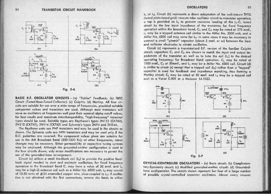
84 TRANSISTOR CIRCUIT HANDBOOKOSCILLATORS 85
(a) (b)
RFC2.5 MHY
(C)
C40.02
Fig. 5-6
BASIC R.F. OSCILLATOR CIRCUITS - (a) "Tickler" Feedback; (b) TBTCCircuit (Tuned -Base -Tuned -Collector); (c) Colpitts; (d) Hartley. All four cir-cuits are suitable for use over a wide range of frequencies, provided suitablecomponent values and transistors are used. Although most transistors willserve as oscillators at frequencies well past their nominal alpha cutoff values,for best results and maximum interchangeability, "high -frequency" transistortypes should be used. Suitable types are Raytheon's types 2N112 (CK760),2N113 (CK761), 2N114 (CK762) and Sylvania's types 2N94 and 2N94A.
The Raytheon units are PNP transistors and may be used in the circuits asshown. The Sylvania units are NPN transistors and may be used only if theD.C. polarities are reversed. The component values given are suitable foruse in the AM Broadcast Band (550-1600 Kc); at other frequencies, minorchanges may be necessary. Either permeability or capacitive tuning systemsmay be employed. Although the grounded -emitter configuration is used inthe four circuits shown, only minor modifications are necessary to permit theuse of the grounded -base arrangement.
Circuit (a) utilizes a small feedback coil (L2) to provide the positive feed-back signal needed to start and maintain oscillation; for fixed frequencyoperation in the Broadcast Band C1 may have a value of 50 mmf. and L1may be a high -Q antenna coil such as a Miller No. 6300 unit; Lo may consistof 15-50 turns of X24 enamelled copper wire, close -coupled to Li; if oscilla-tion is not obtained with the first connections, reverse the leads to either
Li or L2. Circuit (b) represents a direct adaptation of the well-known TPTG(tuned -plate -tuned -grid) vacuum tube oscillator circuit to transistor operation;a tap is provided on Li to prevent excessive loading of the L1 -C1 tunedcircuit by the low input impedance of the transistor; for fixed frequencyoperation within the broadcast band, C1 and Co may be rated at 270 mmf.,Li may be a tapped antenna coil similar to the Miller No. 2000 unit, and aMiller No. 6300 coil may serve for L in some cases it may be necessary toconnect a small "gimmic" capacitor (about 5 mmf. or so) between the baseand collector electrodes to obtain oscillation.
Circuit (c) represents a transistorized R.F. version of the familiar Colpittscircuit; capacitors C1 and C2 are chosen to match the input and output im-pedances of the transistor as well as to tune the coil (L1) to the desiredoperating frequency; for Broadcast Band operation, C1 may be rated at1000 mmf., C2 at 50mmf., and Li may be a Miller No. 6300 coil. Circuit (d)is similar to circuit (c) except that a tapped coil (L1) rather than a "tapped"capacitor is used for feedback and impedance matching, thus forming aHartley circuit; Ci may be rated at 50 mmf. and L1 may be a tapped coilsuch as a Vokar C-801 or a Meissner 14-1033.
Fig 5-7
CRYSTAL -CONTROLLED OSCILLATORS - (a) Basic circuit; (b) Complemen-tary -Symmetry circuit; (c) Modified grounded -emitter circuit; (d) Grounded -base configuration. The circuits shown represent but four of a large numberof possible crystal -controlled transistor oscillators. Almost every vacuum
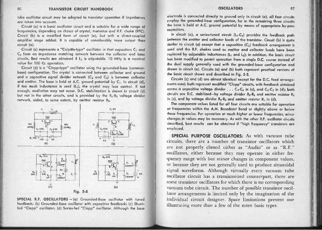
SI; TRANSISTOR CIRCUIT HANDBOOK OSCILLATORS 87
tube oscillator circuit may be adapted to transistor operation if impedancesare taken into account.
Circuit (a) is a basic oscillator circuit and is suitable for a wide range offrequencies, depending on choice of crystal, transistor and R.F. choke (RFC).Circuit (b) is a modified form of circuit (a), but with a direct -coupledamplifier stage added. It is capable of considerably more output thancircuit (a).
Circuit (c) represents a "Colpitts-type" oscillator in that capacitors C1 andC2 form an impedance matching network between the collector and basecircuits. Best results are obtained if L1 is adjustable. 10 MHy is a nominalvalue for 100 Kc operation.
Circuit (d) is a "Clapp -type" oscillator using the grounded -base (common -base) configuration. The crystal is connected between collector and groundand a capacitive signal divider network (C2 and C:3) is between collectorand emitter. The base is held at A.C. ground potential by C1. In circuit (d),if too much inductance is used (L1), the crystal may lose control. If notenough, oscillation may not occur. D.C. stabilization is shown in circuit (d)but not in the other circuits, and is provided by the R1 -R3 voltage dividernetwork, aided, to some extent, by emitter resistor R3.
C,
RFC
25 PANy
C,-50
R422K
(c)
CI,4.7K
270MmF
6Y.
270MAIF
Rj22K
(d)
Fig. 5-8
SPECIAL R.F. OSCILLATORS - (a) Grounded -Base oscillator with tunedfeedback; (b) Grounded -Base oscillator with capacitive feedback; (c) Shunt -fed "Clapp" oscillator; (d) Series -fed "Clapp" oscillator. Although the base
electrode is connected directly to ground only in circuit (a), all four circuitsemploy the grounded -base configuration, for in the remaining three circuitsthe base is held at A.C. ground potential by means of appropriate by-passcapacitors.
In circuit (a), a series -tuned circuit (11-C1) provides the feedback pathbetween the emitter and collector loads of the transistor. Circuit (b) is quitesimilar to circuit (a) except that a capacitive (C1) feedback arrangement isused and the R.F. chokes used as emitter and collector loads have beenreplaced by adjustable inductances (Li and 10); in addition, the basic circuithas been modified to permit operation from a single D.C. source instead ofthe dual supply generally used with the grounded -base configuration andshown in circuit (a). Circuits (a) and (b) both represent practical versions ofthe basic circuit shown and described in Fig. 5-5.
Circuits (c) and (d) are almost identical except for the D.C. feed arrange-ments used; both represent modified "Clapp" circuits, with feedback obtainedacross a capacitive voltage divider . . . C2 -C3 in (c), and C1 -C2 in (d); bothcircuits are D.C. stabilized-by voltage divider R3 -R4 and emitter resistor R2in (c), and by voltage divider R2 -R3 and emitter resistor R1 in (d).
The component values listed for all four circuits are suitable for operationat frequencies within the A.M. Broadcast Band or slightly above or belowthese frequencies. For operation at much higher or lower frequencies, minorchanges in values may be necessary. As with the other R.F. oscillator circuitsdescribed, best results can be obtained if "high frequency" transistors areemployed.
SPECIAL PURPOSE OSCILLATORS: As with vacuum tubecircuits, there are a number of transistor oscillators whichare not properly classed either as "Audio" or as "R.F."oscillators, either because they may operate in either fre-quency range with but minor changes in component values,or because they are not generally used to produce sinusoidalsignal waveforms. Although virtually every vacuum tubeoscillator circuit has a transistorized counterpart, there aresome transistor oscillators for which there is no correspondingvacuum tube circuit. The number of possible transistor oscil-lator arrangements is limited only by the imagination of theindividual circuit designer. Space limitations prevent ourillustrating more than a few of the more basic types.

88 TRANSISTOR CIRCUIT HANDBOOK OSCILLATORS 89
Fig. 5-9
EMITTER -COUPLED MULTIVIBRATORS - (a) Basic Emitter -Coupled circuit;(b) Sawtooth waveform circuit; (c) Adjustable stability circuit; (d) Direct -coupled circuit. The emitter -coupled transistor multivibrator is roughly analo-gous to the cathode -coupled vacuum tube multivibrator.
The basic emitter -coupled circuit is given at (a). Circuit (b) represents thebasic circuit modified to supply a sawtooth output signal; the essentialmodification is the addition of a standard R -C "charge -discharge" circuit(R3 -C3) as part of the collector load of the second transistor-in operation,C3 is charged slowly through R3, then discharged rapidly as the second tran-sistor switches from a non -conducting to a conducting state. Circuit (c) is
another version of the basic circuit, but with an adjustable emitter resistor(R3) to permit a control on circuit stability. Circuit (d) is similar to circuit (c)but illustrates the use of direct -coupling between stages.
In all four circuits, the first transistor is connected using the grounded -baseconfiguration, the second transistor using the common -emitter arrangement;note that the base of the first transistor is heavily by-passed to ground inevery case. Thus, with the exception of circuit (b), all the circuits shown oper-ate in essentially the same fashion . . . several versions are given simply toillustrate a few of the many modifications possible. Basic signal waveformsare shown.
Component values may be varied to change the frequency of operationas well as the symmetry and exact waveform of the signals produced . . .
operating frequencies are not listed, since they will vary with the transistors
used. If desired, any of the circuits may be "locked -in" with an externalsignal by applying an appropriate sync pulse to the ungrounded collectoror base electrodes (collector of first transistor, base of second) or to theemitter circuit.
R,
22K12Me9
(b)
Fig. 5-10
COLLECTOR -COUPLED MULTIVIBRATORS - (a) Basic Collector -CoupledCircuit; (b) Complementary -symmetry circuit. Circuit (a) is a transistorizedversion of the familiar plate -coupled vacuum tube multivibrator, but circuit(b) is unique to transistor circuitry-there is no analogous vacuum tube ar-rangement, for circuit (b) utilizes the complementary symmetrical character-istics of transistors of different types.
The grounded -emitter configuration is used in both circuits. Either circuitmay be synchronized with external signals; the sync signal may be appliedeither to the base or collector electrodes of either transistor in circuit (a); incircuit (b) the sync signal may be applied to the common collector -base con-nection between stages.
In circuit (a), if the collector load resistors, base resistors, and couplingcapacitors are made equal (i.e., R1 = R3, R2 = R4, C1 = C2), and similartransistors are used, the resulting signal will have a symmetrical time division;a non -symmetrical signal (pulse) will result if corresponding parameters arenot equal, with the degree of non -symmetry proportional to the differencesin values between corresponding components. In circuit (b), the comple-mentary symmetrical properties of PNP and NPN transistors are utilized toprovide direct interstage coupling, resulting in a multivibrator circuit with aminimum of components.
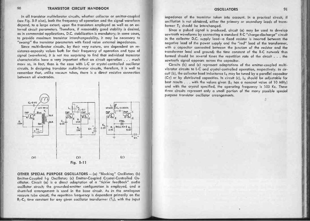
90 TRANSISTOR CIRCUIT HANDBOOK OSCILLATORS 91
In all transistor multivibrator circuits, whether collector or emitter -coupled(see Fig. 5-9 also), both the frequency of operation and the signal waveformdepend, to a large extent, upon the transistors employed as well as on ex-ternal circuit parameters. Therefore, if reasonably good stability is desired,as in commercial applications, D.C. stabilization is mandatory; in some cases,to provide maximum transistor interchangeability, it may be necessary to"swamp" the transistor parameters with fixed value external impedances.
Since multivibrator circuits, by their very nature, are dependent on re-sistance -capacity values both for their frequency of operation and type ofsignal (waveform), it is not too surprising to find that individual transistorcharacteristics have a very important effect on circuit operation . . . much
more so, in fact, than is the case with L -C or crystal -controlled oscillatorcircuits. In designing transistor multivibrator circuits, therefore, it is well toremember that, unlike vacuum tubes, there is a direct resistive connectionbetween all electrodes.
R,220K
Cr 0.02
UTC 50-3
TlPNP Blue
(a)
3V
BLK
BLK0.25
(b)
Fig. 5-11
c20.25
L,10 MNY 0.0005
PNP PNP C
irkX.7
R,2.7K
E
XTAL
Bliley KV-3 R25,6K
B
(C)
6
OTHER SPECIAL PURPOSE OSCILLATORS - (a) "Blocking" Oscillator; (b)Emitter -Coupled l -g Oscillator; (c) Emitter -Coupled Crystal -Controlled Os-cillator. Circuit (a) is a direct adaptation of a "tickler feedback" audiooscillator circuit; the grounded -emitter configuration is employed, and ashunt -fed arrangement is used in the base circuit. As in the analogousvacuum tube circuit, the repetition frequency is dependent primarily on theR1 -C1 time constant for any given oscillator transformer (Ti), with the input
impedance of the transistor taken into account. In a practical circuit, ifoscillation is not obtained, either the primary or secondary leads of trans-former Ti should be interchanged.
Since a pulsed signal is produced, circuit (a) may be used to developsawtooth waveforms by connecting a standard R -C "charge -discharge" circuitin the collector D.C. supply lead-a fixed resistor is inserted between thenegative lead of the power supply and the "red" lead of the transformer,with a capacitor connected between the junction of the resistor and thetransformer lead and ground; the time constant of the R -C network thusformed should be several times the repetition rate of the circuit . . . thesawtooth signal appears across the capacitor.
Circuits (b) and (c) represent adaptations of the emitter -coupled multi -vibrator circuits to L -C and crystal -controlled operation, respectively. In cir-cuit (b), the collector load inductance Li may be tuned by a parallel capacitor(CT) or by distributed capacities. In circuit (c), Ll should be adjustable forbest results . . . with the values given (Li has a nominal value of 10 MHy)and with the crystal specified, the operating frequency is 100 Kc. Thesethree circuits represent only a small portion of the many possible specialpurpose transistor oscillator arrangements.
92 TRANSISTOR CIRCUIT HANDBOOK
Credit: RCA Victor, Division of Radio Corporation of America.
FINAL EXAM - Highly sensitive and exacting electronic test instrumentspass on RCA transistors before they are graduated from the company's plant.Above, a skilled technician is surrounded by layers of finished transistorswhich are to be put over the final production hurdle.
PART II - BASIC CIRCUITS
Chapter 6
SPECIAL PURPOSE CIRCUITS
Like the vacuum tube, the transistor is by no means limitedto amplifier and oscillator circuit applications. There are alarge number of transistor circuits which cannot be groupedconveniently with either Amplifiers or Oscillators. These in-clude such circuits as detectors, clipper -limiters, mixers, andflip-flops, as well as circuits for special transistor types suchas phototransistors and junction tetrodes. For convenience inlisting, all of these circuits are grouped together in this chap-ter as SPECIAL PURPOSE CIRCUITS, even though the individualcircuit types may not be related; a number of Test Circuitsare included also.
In referring to these circuits, it is well to remember that thetransistor is basically an amplifying device and that virtuallyall practical circuits utilize this characteristic in some way.Hence, the three basic amplifier configurations - grounded -base, grounded -emitter, and grounded -collector - are funda-mental to all transistor circuits. For example, a good manyamplifier circuits are shown in Chapter 4, but any of thesemay be classified as belonging to one of the three basic con-figurations, with the only real difference between circuits re-siding in the nature of the loads used, in the Class of operation(A, B, etc.), in the interstage coupling methods used, andwhether or not degenerative feedback is employed. Again, theoscillator circuits illustrated in Chapter 5 are but amplifierswith regenerative feedback between their input and outputterminations.
In an analogous manner, the "Special Purpose" circuitsshown in this chapter might be classed according to the threebasic amplifier configurations and discussed as amplifiers or
93

94 TRANSISTOR CIRCUIT HANDBOOK
oscillators with special characteristics. A limiter then becomesan overdriven amplifier, a detector or mixer a non-linearamplifier, and a flip-flop an oscillator with insufficient feed-back to maintain oscillation. However, for purposes of illus-tration and discussion, we will follow conventional terminol-ogy in labeling and grouping the circuits.
DETECTORS, CLIPPERS AND LIMITERS: In a broad sense, de-tectors, clippers and limiters are all non-linear amplifiers,although the gain, in some cases, may be less than unity. Ifthe term "amplifier" is restricted only to those circuits whichprovide a gain greater than one, then the expression might bechanged from "non-linear amplifiers" to "non-linear devices."Almost every amplifier circuit is non-linear to some degree,and it is this non -linearity which introduces distortion. Fromthe viewpoint of fidelity, a "good" amplifier is one which hasa close approach to perfectly linear operation; from the view-point of the circuit designer requiring detection or clipping,the opposite may be true. Thus, a "poor" amplifier may be a"good" detector or clipper. A single -ended Class B or Class Camplifier makes an excellent clipper, for example. Detectors,clippers, and limiters all employ similar circuits and are simi-lar in operation. The chief difference in these three devices isin their application. A detector is a non-linear device used todemodulate an R.F. signal; it generally accomplishes thisfunction by removing either the positive or the negative -goinghalf of the modulated R.F. signal, allowing a pulsating D.C.to flow through its load impedance; the average value of thepulsating D.C. varies with the modulation. A clipper serves to"chop off" or remove a portion of an applied A.C. signal-itmay be either the positive or negative -going half of the signal,or one or both peaks. A limiter is a specialized type of clipperused to limit the positive and negative peaks of an appliedsignal.
SPECIAL PURPOSE CIRCUITS
PNP
Fig. 6-1
95
Audio Output
SIMPLE R. F. DETECTOR - The detector circuit shown is essentially agrounded -emitter amplifier stage operated without base bias current. In
operation, with no signal applied, D.C. through the collector load is at aminimum. A modulated R.F. signal, supplied by R.F. transformer Tl, is appliedto the base; with a PNP transistor, the positive -going half cycles of the ap-plied signal have relatively little effect on the transistor, since they are ofthe wrong polarity to produce base current flow; the negative -going halfcycles, on the other hand, do produce base current flow and this, in turn,permits the collector current to increase. Without collector capacitor C1, thecollector current would consist of a series of half -wave pulses, with a repe-tition rate equal to the frequency of the applied R.F. signal, and an instan-taneous amplitude proportional to the peak value of each cycle. CapacitorC1 acts to smooth out these pulses, however, so that the collector current hasan average value proportional to the amplitude of the applied signal andan instantaneous value which varies with the modulation envelope of thesignal. Thus, the voltage developed across the collector load, due to thevarying collector current, is a composite signal with both A.C. and D.C.components.
The A.C. component may be obtained through an appropriate D.C. block-ing capacitor and is the demoduated audio or video signal; the D.C. com-ponent is proportional to the R.F. carrier amplitude and may be passedthrough an appropriate R -C filter and used for AVC purposes. In practice,the load is generally a resistor, but, in some applications, may be an audiochoke; in simple receivers, the load may be a pair of high impedanceheadphones.
Another way of analyzing the circuit action is to consider that the base -emitter circuit acts as a simple junction diode as far as the applied R.F. signalis concerned ... thus, the detection action is similar to that obtained with aconventional diode detector, but followed by a direct -coupled amplifier.
Somewhat greater gain can be obtained if a small bias current is appliedto the base (see Fig. 4-17, Chapter 4), but care must be taken that the biascurrent is not great enough to move the operating point to a linear portion

96 TRANSISTOR CIRCUIT HANDBOOK SPECIAL PURPOSE CIRCUITS 9 7
of the transistor's characteristic curves . . . otherwise, the transistor will nolonger act as a detector and will become, instead, an inefficient amplifier.
0.025 PNP
(0)
Pulsesout
III- 6V.
(b)
(c
Fig. 6-2
(d)
CLIPPERS AND LIMITERS - (a) Simple Clipper; (b) Biased Clipper -Limiter;(c) Square -Wave Clipper; (d) Complementary Symmetry Clipper. The
grounded -emitter configuration is used in all four circuits. Circuit (a) is anunbiased (Class B) amplifier and, with a PNP transistor, "clips" the positivehalf cycles of an applied signal. Except for the use of an R -C input arrange-ment, the circuit is almost identical to the Simple R.F. Detector shown in Fig.6-1, and its operation is similar. Collector current is at a minimum with zeroinput signal. Positive -going pulses appear across collector load Ro. With alow input signal level, the pulses have rounded peaks (assuming sine-waveinput); as the input level is increased, the peak collector current also increasesuntil the full source voltage is dropped across Ro; this represents collectorcurrent "saturation" and, at this point, the output pulses acquire flat tops.Thus, with proper drive, rectangular pulses appear across R2.
Circuit (b) is a clipper circuit using a "saturated" amplifier rather than anunbiased one ... in a way, its operation is just the opposite of that of circuit(a). The base resistor R1 is returned to the "hot" side of the power source,establishing a bias current; R1 is then made fairly small, increasing both biasand collector current until "saturation" occurs and virtually the full sourcevoltage is dropped across collector load R. Thus, in circuit (b), collectorcurrent is at a maximum with zero input signal.
With a PNP transistor, this circuit "clips" the negative half cycles of anapplied signal. Negative -going pulses appear across collector load R2; theseare rounded at low signal levels but become rectangular as drive is in-creased. Both circuits (a) and (b) have low input impedances and will givetheir best results when driven with a moderate to low impedance source.Circuit (c) is similar in operation to circuit (a) but with one modification; aresistor (R1) has been added in series with the input lead. This resistor servesa dual purpose ... first, it increases the input impedance of the circuit, thusminimizing the loading effect on the signal source, and, secondly, it improvesthe clipping action of the circuit.
The output of circuit (c), when properly driven, closely approaches asymmetrical rectangular waveform or square -wave, as contrasted to thecomparatively narrow pulses produced by circuit (a). Square -waves may alsobe obtained from circuit (d), which is essentially the clipper circuit shown at(c) direct -coupled to an additional clipper -amplifier stage. Different typetransistors are employed to take advantage of the complementary symmetryprinciple in direct -coupling the two stages.
MIXER -CONVERTERS: When two signals are combined in anon-linear device, the output is a complex signal waveformcontaining the frequencies of both original signals, plus theirsum and difference frequencies, plus harmonics. By providinga tuned output load, any one of these different frequenciesmay be selected. In superheterodyne receiver applications, thedifference frequency is the one generally used, and it then be-comes the I.F. signal for the receiver. Since non-linear opera-tion is essential to the mixing action, a detector circuit per-forms well as a mixer, provided a resonant circuit is substitutedfor the resistive load. The resonant circuit serves two func-tions-(1) it selects the desired I.F. signal and (2) by virtue ofits "fly -wheel" action, it recreates a complete signal from thepulses which the detector supplies. In a radio receiver, oneof the two input signals is the desired broadcast signal, theother is a locally generated R.F. signal, provided by a separateoscillator. Of course, it is possible to combine the oscillatorand mixer actions in one circuit, in which case the compositecircuit may be termed a converter, for it "converts" incomingR.F. signals to a fixed I.F. signal. Since the action of either amixer or a converter is similar to that of a detector, it is com-

98 TRANSISTOR CIRCUIT HANDBOOK SPECIAL PURPOSE CIRCUITS 99
mon practice to call this stage the "1st Detector" in super-heterodyne receivers.
(b)
Fig. 6-3
MIXER AND CONVERTER - (a) Basic Mixer; (b) Triode Converter. Thegrounded -emitter configuration is used in both circuits. The component valuesspecified are for operation at frequencies within the A.M. Broadcast Bandand for I.F.s below 500 Kc. different values may be required at higher or.ower frequencies. For maximum conversion gain, "high frequency" transistortypes should be used.
In circuit (a), the input R.F. signal is selected by the Li -C1 resonant circuit;Li may be an antenna coil, tapped down for proper impedance match to thetransistor's input circuit. The signal from the local oscillator is applied to thebase through capacitor C2. Mixing action occurs within the transistor, whichis operated without bias. The output I.F. signal appears across the primaryof the I.F. transformer
A typical commercial coil for Li is a MILLER #2000 Transistor Loop An-tenna, for Ti a VOKAR #T-101 I.F. transformer. In circuit (b), a single tran-sistor is used both as an oscillator and as a mixer. A modified "tickler feed-back" oscillator circuit is employed, with 12, in the collector circuit, inductivelycoupled to L3, in the emitter circuit. The take -off point on 13 is tapped downto permit a better impedance match to the transistor and thus to reduce theloading on the L3 -C2 oscillator tuned circuit. As in the mixer, tuned circuit
11-C1 selects the incoming R.F. signals; tuning capacitor C1, in the preselectorcircuit, and C2, in the oscillator circuit, are generally ganged together inpractical circuit applications. In a typical experimental circuit, Li and T1may be the coils specified for circuit (a), and T2 may be a VOKAR #C-801oscillator transformer.
GATES AND FLIP-FLOPS: A multivibrator circuit which isunable to sustain oscillation, either because of insufficientfeedback or improper bias, can often be thrown out of itsstable non -oscillating condition by the application of a strongexternal signal or trigger. Depending on the application and onthe circuit arrangement used, two types of operation are gen-erally encountered. In a gate or monostable* circuit, the cir-cuit remains inactive until a strong trigger signal is applied atthe proper input point. The circuit then changes from its stablenon -oscillating condition to an unstable condition tempo-rarily; after a period of time determined by circuit parameters,the circuit returns to its stable condition. In the majorityof applications, the period required for the circuit to returnto a stable condition is made equal to one cycle of oscillation,so that a single output pulse is obtained for each input triggerpulse. In a flip-flop or bistable arrangement, the circuit hastwo stable conditions, and can be switched from one to theother by the application of appropriate trigger pulses at theproper points. Two input pulses are required to return thecircuit to its original stable state, and hence such a circuit maybe used as a binary (scale -of -two) counter. Application -wise,monostable circuits are generally used for pulse formation,producing output signals of known waveform, duration andamplitude from varying input signals; bistable circuits aremore generally used in counter applications. Because of theirsmall physical size, long life, and minute power requirements,transistors are ideal for use in monostable and bistable circuits,especially where such circuits are used in compact militaryequipment or in complex computers.
*A monostable or gate circuit is often called a "one shot multivibrator" or"univibrator."

100 TRANSISTOR CIRCUIT HANDBOOK SPECIAL PURPOSE CIRCUITS 101
Cz-0.01
(c)
Fig. 6-4
4 7K
MONOSTABLE CIRCUITS - (a) Collector -Coupled; (b) Emitter -Coupled; (c)"Complementary Symmetry" Collector -Coupled. All three circuits are directadaptations from corresponding multivibrator circuits.
In circuit (a), the output pulse generally is obtained across the collectorload resistor R2; the input trigger is applied through C1. The adjustment ofR4 determines the stability of the circuit; with some transistors, R., may beadjusted for free -running multivibrator action, in which case there may betwo regions of monostable action, one on either side of the adjustment whereoscillation takes place. Pulses of opposite polarity are produced, dependingon which monostable adjustment is chosen.
In circuit (b), the output pulse appears across collector load R.,2; the inputtrigger is applied through Co to the common emitter circuit. The adjustmentof R3 establishes the bias on the second transistor and thus determineswhether free -running or monostable action is obtained.
Circuit (c) utilizes the complementary symmetrical characteristics of tran-sistors of different types to permit direct -coupling between stages. The outputpulse is obtained across collector load Ro; the input trigger is applied to thecommon collector -base connection through capacitor C1. This circuit is quitesimilar to the multivibrator circuit shown in Chapter 5 (Fig. 5-10) with butone small change ... base resistor R1 is returned to the negative side of thepower supply, thus heavily biasing the first transistor and stabilizing thecircuit. The circuit remains stable until a trigger pulse is applied, then goesthrough its cycle of operation and returns to its stable state.
The basic operation of all three circuits is similar in that all three aremultivibrators which have been stabilized in a non -oscillating state by the
application of proper bias currents. In circuit (a), adjusting R4 sets the bias
for the second transistor; in circuit (b), adjusting R3 sets the bias for thesecond transistor; and in circuit (c), returning the base resistor R1 to the "hot"side of the power source establishes the bias current for the first transistor.Again, in all three circuits, the application of a trigger pulse initiates acumulative change in circuit operation which is sustained only by the R -Ctime constant of the coupling circuits so that the circuits eventually return totheir normal stable state.
R,3100K IN34A 8.
R22K 8.2K
0 II
C,-SOMMF
4-z
a.
0101
IN34A
R850K
C
PNP
R - 33K
Cz-470MMF
-C4 R6
0.01 39K
C3 470MMF
R739K
6 V.
C
PN P
E
Fig. 6-5
BISTABLE CIRCUIT - This circuit represents a transistorized version of afamiliar vacuum tube binary counter. In essence, it is a non -oscillating collec-tor -coupled multivibrator which has two stable states, and which can betransferred from one state to the other by the application of an appropriatetrigger pulse. In operation, one or the other of the two transistors startsconducting first.
For purposes of discussion, let us say it is the left-hand transistor. As col-lector current flows, a voltage drop occurs across the collector load resistorRo, reducing the potential available for supplying base bias current to thesecond transistor through voltage divider RI -R7. At the same time, the emittercurrent flowing through resistor Rs develops a voltage which tends to opposenormal base bias current flow in the right-hand transistor.
Since collector current is limited in the right-hand transistor, due to thelack of proper base bias, comparatively little voltage drop occurs across
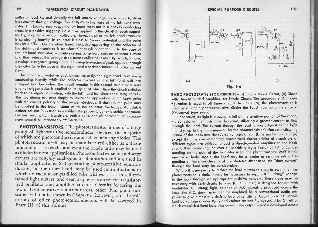
102 TRANSISTOR CIRCUIT HANDBOOK SPECIAL PURPOSE CIRCUITS 103
collector load R3, and virtually the full source voltage is available to drivebias current through voltage divider R5 -R6 to the base of the left-hand tran-sistor. This bias current keeps the left hand transistor in a heavily conductingstate. If a positive trigger pulse is now applied to the circuit through capaci-tor C1, it appears on both collectors. However, since the left-hand transistoris conducting heavily, its collector is close to ground potential and the pulsehas little effect. On the other hand, the pulse appearing on the collector ofthe right-hand transistor is transferred through capacitor C3 to the base ofthe left-hand transistor; a positive -going pulse here reduces collector currentand thus reduces the voltage drop across collector resistor R2, which, in turn,develops a negative -going signal. This negative -going signal, applied throughcapacitor C2 to the base of the right-hand transistor, intiates collector currentflow.
The action is cumulative and, almost instantly, the right-hand transistor isconducting heavily while the collector current in the left-hand unit hasdropped to a low value. The circuit remains in this second stable state untilanother trigger pulse is applied to its input, at which time the circuit switchesback to its original operation, with the left-hand transistor conducting heavily.The two diodes are used simply to insure the application of a trigger pulsewith the correct polarity to the proper electrode; if desired, the pulse maybe applied to the base instead of to the collector electrodes. Adjustableemitter resistor R8 is used to establish the proper bias for bistable operation.For best results, both transistors, both diodes, and all corresponding compo-nents should be reasonably well -matched.
PHOTOTRANSISTORS: The phototransistor is one of a largegroup of light-sensitive semiconductor devices, the majorityof which are photoconductive and self-generating diodes. Thephototransistor itself may be manufactured either as a diodejunction or as a triode, and even the triode units may be usedas diodes in most applications. Photoconductive semiconductordevices are roughly analogous to phototubes and are used insimilar applications. Self -generating photo -sensitive semicon-ductors, on the other hand, may be used in applications inwhich no vacuum or gas -filled tube will work . . . in self-con-tained light meters, and even as power sources for transistor-ized oscillator and amplifier circuits. Circuits featuring theuse of light sensitive semiconductors, other than phototran-sistors, will not be shown in Chapter 6; however, typical appli-cations of other photo -semiconductors will be covered inPART III of this volume.
Light(steady)!
Not Used
PNP NPN
Light(steady)
rB
Not Used
(b)
Fig. 6-6
BASIC PHOTOTRANSISTOR CIRCUITS-(a) Simple Diode Circuit; (b) Diodewith Direct -Coupled Amplifier; (c) Triode Circuit. The grounded -emitter con-figuration is used in all three circuits. In circuit (a), the phototransistor isused as a simple photoconductive diode; the Load may be a meter or aD'Arsonval type relay.
In operation, as light is allowed to fall on the sensitive portion of the diode,the collector -emitter resistance decreases, allowing a greater current to flowthrough the load. The current through the load is proportional to the lightintensity, up to the limits imposed by the phototransistor's characteristics, the
nature of the load, and the source voltage. Circuit (b) is similar to circuit (a)except that the complementary symmetrical characteristics of transistors ofdifferent types are utilized to add a direct -coupled amplifier to the basiccircuit, thus increasing the over-all sensitivity by a factor of 10 to 50, de-pending on the gain of the transistor used; the phototransistor itself is still
used as a diode. Again, the Load may be a meter or sensitive relay. De-pending on the characteristics of the phototransistor used, the "dark current"through the load may be considerable.
Where it is necessary to reduce the load current to close to zero when thephototransistor is dark, it may be necessary to supply a "bucking" voltageto the load through an appropriate resistive network. These steps may benecessary with both circuits (a) and (b). Circuit (c) is designed for use withmodulated (pulsating) light, so that an A.C. signal is produced across theload; the A.C. signal may then be amplified by a conventional audio am-plifier to give almost any desired level of sensitivity. Circuit (c) is D.C. stabil-ized by voltage divider R3 -R4 and emitter resistor R1, bypassed by C1, all ofwhich establish a fixed base bias current. The output signal is developed across
Light(pulsating)
L,UTAII*1747
R4- 100K
(a) (c)

104 TRANSISTOR CIRCUIT HANDBOOK SPECIAL PURPOSE CIRCUITS 105
collector load resistor R2. A choke (Li) is used in the base circuit, but is notabsolutely essential to circuit operation unless R3 and R4 have low values.
For maximum sensitivity to a specific light signal, base choke L1 may betuned to the light's modulating frequency by an appropriate parallel capaci-tor, and collector load R2 may be replaced by a resonant circuit, again tunedto the same frequency. In all three circuits, the overall sensitivity may be in-creased considerably by using a lens system to concentrate incoming lighton the most sensitive portion of the phototransistor's surface.
JUNCTION TETRODES: At the present writing tetrode tran-sistors are produced commercially by just a few manufacturersand are available only in a limited number of types. Thislimited availability prompts the author to list tetrode circuitsas Special Purpose Circuits at this time and to group themtogether in this Chapter. In the future, perhaps even in a lateredition of this volume, the author feels that junction tetrodetransistors will join their older triode "brothers" as standarddevices, and that, at that time, tetrode circuits may be groupedappropriately with corresponding triode amplifiers and oscil-lators. Currently available tetrode transistors are, in effect,"double -base" triodes, for two connections are made to thebase electrode. In most applications the second base is biasedwith reverse current. This bias, in turn, repels charges travel-ing from the emitter and narrows the area over which currentcan travel through the base. Since the major conduction isforced to take place in the region close to the normal baseconnection, diffusion is kept to a minimum and transistoraction is limited to this region. The net effect is to lower thebase resistance considerably (in the grounded -base configura-tion), allowing the transistor to be used at much higher fre-quencies than would be possible otherwise. Of course, thesecond base connection may be used for other purposes also. . . for inserting a modulation signal, for gain control, formixing two signals, and in similar applications. A tetrode maybe used as a triode, if desired, simply by allowing one ofthe base connections to "float." In such cases, different triodecharacteristics are obtained, depending on which base con-nection is used.
BIAS(b
C4
(c)
Fig. 6-7
BASIC TETRODE CIRCUITS - (a) Amplifier; (b) Mixer; (c) Oscillator; (d)Converter. The grounded -base configuration is used in all four circuits. Com-ponent values are not specified for these basic circuits, for exact values will
vary considerably with the types of transistors used and the exact operatingconditions desired; however, in most cases, the D.C. operating voltages andcurrents of the emitter and collector circuits are about the same as for acorresponding triode, while the second base (B2) current will be on the orderof from 0 to 2.0 milliamperes . .. note that the second base is biased with apolarity opposite that of the regular base (B1).
The basic circuit shown at (a) may be used as a wide -band resistance -coupled amplifier or as an R.F. amplifier; as an R.F. amplifier, the emitter(R1), and collector (R3) loads may be replaced by inductive or resonant cir-cuits; as a wide -band resistance -coupled amplifier, the bandwidth may beextended by making collector load R3 smaller and smaller, but only at theexpense of reduced gain at lower frequencies. With presently availabletransistors, bandwidths of 5 to 10 me (to 3 db point) are not uncommon, withgains in the neighborhood of 15 to 25 db.
Circuit (b) may be used for mixing two R.F. signals to produce an I.F.signal, which appears across resonant circuit 1.1-05. One signal is applied tothe emitter circuit, the other to the second base.
Circuit (c) is a typical R.F. oscillator arrangement, using a modified Hartleycircuit; with presently available transistors, operating frequencies in excess

106 TRANSISTOR CIRCUIT HANDBOOK SPECIAL PURPOSE CIRCUITS 107
of 100 Mc may be obtained without great difficulty. Circuit (d) combines a"tickler feedback" oscillator and mixer into one circuit to provide an I.F.converter. The feedback signal necessary to start and sustain oscillation isobtained from coil 12, inductively coupled to 1.3, in the collector circuit.Resonant circuit L1 -C1 is tuned to the incoming R.F. signal, 13-C4 to the oscilla-tor frequency, and the primary of Ti to the I.F. value. R.F. coil Li is tappeddown to permit an impedance match to the comparatively low input imped-ance of the stage, and thus to minimize loading on the tuned circuit.
C,50MMF NPN
R,18K
Fig. 6-8
TETRODE OSCILLATOR (Fig. 6-8) -A breadboarded version of the circuitshown gave good results as an R.F. oscillator, operating over the rangeof 16 to 25 Mc. A GERMANIUM PRODUCTS CORP. type 3N23 tetrode junc-tion transistor was used in the author's experimental circuit; Li was a standardTV I.F. "transformer" coil to which four turns of #30 insulated copper wirewere added for feedback purposes. The circuit is a modified Hartley oscilla-tor arrangement, using a grounded -emitter configuration. In operation, Li
forms a resonant circuit with its own and circuit distributed capacities; tuningis by means of the coil's (Li) powdered iron core.
The first base (B1) is shunt -fed, with the feedback signal applied throughcapacitor C1 and bias current supplied through base resistor R1, which re-turns to the positive side of the power source. Thus, the first base is positivewith respect to the emitter, and has the correct polarity for a grounded -emitter NPN stage. Emitter resistor R2, by-passed by capacitor C2, has a dualpurpose; first, it serves to provide a degree of D.C. stabilization; secondly,it serves to provide the proper bias for the second base (B2). The second basereturns directly to ground. The voltage drop across R2 due to emitter currentraises the emitter slightly above ground in a positive direction. Thus, thesecond base is negative with respect to the emitter, and thus is biased withthe opposite D.C. polarity of the first base. Capacitor C3 serves as a by-passacross the power source. This circuit may be modulated by inserting the
modulating signal in series with the D.C. supply lead to coil Li.
TEST CIRCUITS: Techniques and circuits which are usefulfor testing transistors and transistorized equipment fall intotwo general groupings . . . (1) those which are basic to labora-
tory practice and which may be used for testing any type ofelectronic equipment, whether transistor or vacuum tubeoperated, and (2) those specifically designed for determiningtransistor characteristics and performance. As far as a tran-sistor's operation in a specific circuit is concerned, basic infor-mation relative to its performance characteristics may be givenby indicating all D.C. electrode voltages and currents as wellas specifying the circuit's performance; D.C. voltages andcurrents are referred to the common or grounded electrode,whether it be the base, emitter, or collector. Individual transis-tor characteristics, irrespective of specific circuit operation, maybe given by families of characteristic curves; typical familiesmay be prepared for each basic circuit configuration; for thegrounded -base circuit, the following groupings may be used . . .
(a) Emitter Voltage vs. Emitter Current for a fixed CollectorCurrent (Input Characteristic); (b) Collector Voltage vs. Col-lector Current for a fixed Emitter Current (Output Character-istic); (c) Emitter Current vs. Collector Voltage for a constantCollector Current (Forward Characteristic); (d) CollectorCurrent vs. Emitter Voltage for a constant Emitter Current

108 TRANSISTOR CIRCUIT HANDBOOK
(Feedback Characteristic). Similar families of curves may beprepared for the grounded -emitter configuration, in whichcase the base electrode is substituted for the emitter in eachgrouping. Unless special techniques are employed, preparingfamilies of characteristic curves is, at the best, a time consum-ing process, requiring from scores to hundreds of individualmeasurements and a final careful plotting of points on appro-priate graphs (refer to the section TESTING TRANSIS-TORS in Chapter 2-TECHNIQUES). For a more rapidevaluation of a transistor's characteristics, two methods maybe used . . . (1) the standard "Substitution Test" of the tran-sistor in a desired circuit arrangement as a check on its per-formance and (2) measurement of its essential gain character-istics (alpha and/or beta) and its leakage currents.
SIGNAL
SOURCE
[SIGNAL GEN ]
DRIVEN
DEVICE
[AMPLIFIER]
Fig. 6-9
GAIN & FREQUENCY RESPONSE MEASUREMENT - The circuit arrange-ment shown in block diagram form may be used to check both the overallgain and the frequency response of virtually any signal handling device,whether vacuum tube or transistor operated. The SIGNAL SOURCE suppliesan A.C. voltage of known frequency and amplitude; in most cases, it will bea variable frequency Signal Generator - an Audio Generator is used forchecking audio amplifiers, an R.F. Signal Generator for checking radioreceivers.
The DRIVEN DEVICE is the piece of equipment to be tested ... it may bea single amplifier stage, a complete multi -stage amplifier, a radio receiver,or any similar signal handling equipment. Resistor RL is the normal outputload for the DRIVEN DEVICE. The VTVM is used to check both input andoutput signal amplitudes. To measure gain, use the VTVM to check input andoutput signal amplitudes by transferring the "hot" lead from point "A" topoint "B". Voltage gain may be determined by dividing the output voltageby the input voltage.
Where power gain is desired, its numerical value may be determined by
SPECIAL PURPOSE CIRCUITS 109
taking the input and output impedances into account. Assuming that bothimpedances are resistive, input power may be determined by squaring theinput voltage and dividing by the input impedance; output power may bedetermined by squaring the output voltage and dividing by RL. In both cases,power is in watts, voltages in volts, and resistances in ohms. The numericalpower gain is the output power divided by the input power; however, powergain is generally expressed in db rather than as a numerical ratio. Thepower gain in db is equal to ten times the logarithm (to the base 10) of theratio of output to input powers. Simply obtain the logarithm of the numericalvalue of power gain and multiply by 10.
To measure frequency response, use the VTVM to check input and outputsignal amplitudes as before. The input amplitude is kept constant as thefrequency of the SIGNAL SOURCE is varied over the desired range in dis-crete steps, and the output signal amplitude is measured and recorded ateach point. The set of measurements obtained are then converted into gainfigures, using the methods described above, and the results listed in a tableor plotted on a graph.
When making either gain or frequency response measurements, care mustbe taken that the input signal is kept well below the overload point for theDRIVEN DEVICE being tested.
SIGNAL
SOURCE
R
B
(a)
DRIVEN
DEVICE
[AMPLIFIER, M]
SIGNAL
SOURCE g[AMP. OUTPUT]
(b)
Fig. 6-10IMPEDANCE MEASUREMENTS (a) Input Impedance; (b) Output Imped-ance. Circuit (a) is used to determine the input impedance of any DRIVENDEVICE, such as an audio amplifier, a test instrument, a receiver, or anysimilar equipment driven by an external signal. The same technique may beused both on single stages and on complete equipments.
A SIGNAL SOURCE, VTVM, and a calibrated, non -inductive variable re-sistor (R) are the basic instruments needed. If the DRIVEN DEVICE is an

110 TRANSISTOR CIRCUIT HANDBOOKSPECIAL PURPOSE CIRCUITS 111
amplifier, it should be terminated in its normal load impedance. The SIGNALSOURCE may be a Signal Generator (either audio or R.F., depending on theequipment to be checked) with a low impedance output. If a calibrated re-sistor is not available, any non -inductive variable resistor may be used inits place, provided the resistance setting can be checked accurately with animpedance bridge or similar instrument. To measure the input impedance,use the SIGNAL SOURCE to apply an appropriate signal to the DRIVENDEVICE and calibrated resistor (R) connected in series, taking care not tooverload the input of the equipment.
Use the VTVM to check the signal voltage across both the calibrated re-sistor (R) and the input to the DRIVEN DEVICE by transferring its "hot" leadback and forth between points "A" and "B". Adjust the resistor (R) until thesetwo voltages are equal . . . the exact readings are not too important. Whenthe voltages at points "A" and "B" are equal, the resistance (R) is equal tothe input impedance of the DRIVEN DEVICE.
Circuit (b) is used to determine the output impedance of any SIGNALSOURCE, such as a signal generator, or an amplifier driven with an externalsignal. A VTVM is used to measure the output voltage of the SIGNAL SOURCEunder "no-load" conditions (Swi open). A calibrated, non -inductive resistor(R) is connected across the output (Swi closed) and the signal output, underload, measured with the VTVM. Resistor R is adjusted until the output voltage,under load, is equal to one-half the "no-load" voltage. At this point, R isequal to the output impedance of the SIGNAL SOURCE. As before, if theSIGNAL SOURCE is an amplifier driven by an external signal, care must betaken that the equipment is not overdriven.
The input impedance of transistor circuits varies widely, depending on boththe transistor and on the circuit configuration used. With the grounded -baseconfiguration, the impedance is generally low, ranging from about 25 to1,000 ohms. With the grounded -emitter configuration, the input impedance ismoderate, ranging from 250 to 2500 ohms or more. With the grounded -
collector configuration, the input impedance is high, ranging from 50,000 to500,000 ohms.
The output impedance of the grounded -base configuration is high, gener-ally between 50,000 ohms and 1 megohm. The grounded -emitter configura-tion has a moderately high output impedance, ranging from 5,000 to 50,000ohms. Finally, the grounded -collector circuit (sometimes called an "emitter -follower") has a moderately low output impedance, ranging from 500 to25,000 ohms.
These typical values apply only to low -power junction transistors. Ingeneral, "hi -power" transistors have both low input and low output im-pedances. Typical input impedances may range from 5 to 25 ohms; outputimpedances from 20 to 100 ohms.
(a)
Fig. 6-11
Not Connected
LEAKAGE CURRENTS - (a) Collector -Base (Ico); (b) Collector -Emitter (lobo).
In both circuits, meter M is a microammeter of suitable range. The currentvalues measured may be compared with the transistor's published data at
the test voltages specified by the manufacturer. In both cases, the smaller the
leakage current measured, the better; in addition the currents should not be
erratic. Both currents may tend to increase with age and with increases inambient temperature. Of the two leakage current values, the collector -base
current (leo) should be much the smaller, ranging from 0 to around 20 or 25
microamperes; the collector -emitter leakage current may range as high as
100 to 150 microamperes, but should generally be much smaller. If the
measured leakage currents are excessively high, or if the readings are
erratic, the transistor is probably defective.With NPN transistors, battery polarities and meter connections are re-
versed. The collector -base leakage current with zero emitter current (leo), as
determined with circuit (a), is often called collector saturation current and,
sometimes, collector cut-off current.Silicon transistors have much lower leakage current values than germanium
units. Whereas a good quality germanium transistor may have a saturation
current value ranging up to 5 microamperes, a silicon transistor may have a
saturation current of but a fraction of a microampere. In most practical work,
as long as the saturation current is below one microampere, it can be ignored.

112 TRANSISTOR CIRCUIT HANDBOOK SPECIAL PURPOSE CIRCUITS 113
CONSTANT
CURRENT
SUPPLY
PNP
E ecVOLTAGE
REGULATED
s y
+1
Fig. 6-12
ALPHA MEASUREMENT - (a) Static Measurement; (b) Dynamic Measure-ment. Alpha is the current amplification factor of the transistor in thegrounded -base configuration and may be defined as the ratio of the changein collector current to an incremental change in emitter current at a constantcollector potential. This factor may be determined by either static (D.C.) ordynamic (A.C.) measurements. Both techniques are shown.
In both circuits, M1 and M2 are milliammeters and the CONSTANT CUR-RENT SUPPLIES are either laboratory test units or conventional adjustablevoltage supplies with a large value resistor connected in series (see sectionTESTING TRANSISTORS, Chapter 2-Techniques).
In circuit (a), the VOLTAGE REGULATED SUPPLY may be either an A.C.operated circuit or batteries. In circuit (b), series resistors R1 and R2 are usedsimply to develop small A.C. voltages which can be measured by A.C.VTVMs M3 and M4 . . . suitable values are from 5 to 50 ohms. R1 shouldequal R2. The power supplies should be heavily by-passed to A.C.; this maybe accomplished by connecting high value electrolytic capacitors across theiroutput terminals. The A.C. signal source should have a very low D.C. re-sistance ... in general, this will be the secondary of a step-down transformerdriven by a Signal Generator. The power supply polarities shown in bothcircuits (a) and (b) are for PNP transistors ... for NPN units, reverse powersupply and meter connections.
To measure alpha using the "static" method, as shown at (a), first adjustall D.C. operating voltages and currents to the values suggested by the tran-
sistor manufacturer in his specification sheets. Note the values of emitter andcollector currents. Next, vary the emitter current a small amount (from 0.05
to 0.2 ma), noting the corresponding change in collector current. Alpha isthen the ratio of the difference between the two collector current values to
the difference between the corresponding emitter current values. Differentvalues of alpha may be obtaind for the same transistor, depending on the
initial voltage and current values.To measure alpha using the "dynamic" method, shown at (b), first adjust
all D.C. operating currents to the values suggested by the transistor manu-facturer in his specification sheets. Next, apply a small A.C. signal to the
emitter circuit, as shown (this signal should be a fraction of a volt for mostsmall transistors). Determine the A.C. voltages appearing across R1 (M3) and
R2 (M4). Alpha is then the ratio of the voltage measured by M4 to that indi-cated by M3. The "dynamic" method for measuring alpha is generally used
to determine how alpha varies with frequency and to determine the alphacut-off frequency (fc - frequency at which alpha is 0.707 of its low fre-quency value ... that is, the frequency at which the gain is down 3 db fromits low frequency value).
(0) (b
Fig. 6-13
BETA MEASUREMENT - (a) Static Measurement; (b) Dynamic Measurement.
Beta is the current amplification factor of a transistor in the grounded -emitterconfiguration and may be defined as the ratio of the change in collector
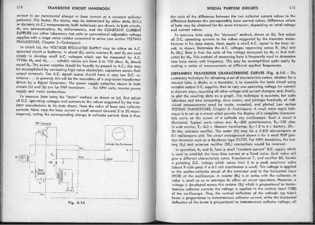
111 TRANSISTOR CIRCUIT HANDBOOK SPECIAL PURPOSE CIRCUITS 115
current to an incremental change in base current at a constant co/lectorpotential. This factor, like alpha, may be determined by either static (D.C.)or dynamic (A.C.) measurements; both techniques are shown. In both circuits,MI are microammeters, M2 milliammeters, and the CONSTANT CURRENTSUPPLIES are either laboratory test units or conventional adjustable voltagesupplies with a large value resistor connected in series (see section TESTINGTRANSISTORS, Chapter 2-Techniques).
In circuit (a), the VOLTAGE REGULATED SUPPLY may be either an A.C.operated circuit or batteries. In circuit (b), series resistors R1 and R2 are usedsimply to develop small A.C. voltages which can be measured by A.C.VTVMs M3 and M4 . . . suitable values are from 5 to 100 ohms. R1 shouldequal R2. The power supplies should be heavily by-passed to A.C.; this maybe accomplished by connecting high value electrolytic capacitors across theiroutput terminals. The A.C. signal source should have a very low D.C. re-sistance ... in general, this will be the secondary of a step-down transformerdriven by a Signal Generator. The power supply polarities shown in bothcircuits (a) and (b) are for PNP transistors ... for NPN units, reverse powersupply and meter connections.
To measure beta using the "static" method, as shown at (a), first adjustall D.C. operating voltages and currents to the values suggested by the tran-sistor manufacturer in his data sheets. Note the value of base and collectorcurrents. Next, vary the base current a small amount (around 5 to 20 micro-amperes), noting the corresponding change in collector current. Beta is then
M Iti I
PNP Transistor
BoseRi Current
!Ver.
Rz
SR, _L
Her.
16nd.
117V.4.C. I
Cathode Ray Oscilloscope
-0 V H
-oGnd.
Fig. 6-14
the ratio of the difference between the two collector current values to thedifference between the corresponding base current values. Difference valuesof beta may be obtained for the same transistor, depending on intial voltageand current values.
To measure beta using the "dynamic" method, shown at (b), first adjustall D.C. operating currents to the values suggested by the transistor manu-facturer in his data sheets. Next, apply a small A.C. signal to the base cir-cuit, as shown. Determine the A.C. voltages appearing across R1 (M3) andR2 (M4). Beta is then the ratio of the voltage measured by M4 to that indi-cated by M3. This method of measuring beta is frequently used to determinehow beta varies with frequency. This may be accomplished quite easily bymaking a series of measurements at different applied frequencies.
OBTAINING TRANSISTOR CHARACTERISTIC CURVES (Fig. 6-14) - Thecustomary technique for obtaining a set of characteristic curves, whether for avacuum tube, a diode, or a transistor, is to assemble the basic circuit usingvariable output D.C. supplies, then to vary one operating voltage (or current)in discrete steps, recording all other voltage and current changes, and, finally,to plot the resulting data on a graph. This technique is accurate, but quitelaborious and time consuming, since scores, and perhaps hundreds, of indi-vidual measurements need be made, recorded, and plotted (see sectionTESTING TRANSISTORS, Chapter 2-Techniques). A much more rapid tech-nique is to set up a circuit which permits the display of a complete character-istic curve on the screen of a cathode ray oscilloscope. Such a circuit is
illustrated. Typical parts values are: R1 -50K potentiometer, R2-100 ohm,1/2 watt resistor, T1-6.3 v. filament transformer, B1-1.5 to 6 v. battery, SRI. -20 Ma. selenium rectifier. The meter (M) may be a 0-500 microampere or0-1 milliampere unit. The circuit arrangement shown is for a small PNP junc-tion transistor such as a Raytheon type CK722. For NPN transistors, the bat-tery (B1) and selenium rectifier (SRO connections would be reversed.
In operation, R1 and B1 form a small "constant current" D.C. supply whichis used to establish the base bias current at a fixed value. Each value willgive a different characteristic curve. Transformer T1 and rectifier SRI furnisha pulsating D.C. voltage which varies from 0 to a peak maximum value(about 9 volts peak if a 6.3 volt transformer is used). This voltage is appliedto the emitter -collector circuit of the transistor and to the horizontal input(HOR) of the oscilloscope. A resistor (R2) is in series with the collector; its
value is small so as to minimize its effect on circuit operation. However, avoltage is developed across this resistor (R2) which is proportional to instan-taneous collector current; this voltage is applied to the vertical input (VER)of the oscilloscope. Thus, the vertical deflection of the cathode ray tube'sbeam is proportional to instantaneous collector current, while the horizontaldeflection of the beam is proportional to instantaneous collector voltage, all

116 TRANSISTOR CIRCUIT HANDBOOK SPECIAL PURPOSE CIRCUITS 117
with a fixed base current. The resulting trace is an accurate output character-istic curve for the transistor in the grounded -emitter configuration (i.e., col-lector voltage vs. collector current for a fixed base current). A similar tech-nique may be used to obtain other types of characteristics curves. The re-sulting curves may be photographed or traced directly from the screen ofthe oscilloscope.
Fig. 6-15
CHARACTERISTIC CURVE GENERATOR - An assembled practical versionof the circuit given in Fig. 6-14. The part of the circuit enclosed by the dottedline has been assembled on a small aluminum chassis for experimental lab.work. The battery (BI) and rheostat (R1) are self-contained; the meter (M)is external, connected to the chassis through the leads shown in the back-ground. Base current is adjusted by the small knob marked "BASE CUR.",which controls the setting of RI. Oscilloscope connections are to the terminalstrip terminals on one side of the chassis; the terminals marked "GND","HOR", and "VER" are connected to corresponding terminals of the oscillo-
scope. The transistor socket used is a special experimental socket of the typeused by transistor manufacturers for production testing of transistors.
Fig. 6-16
For rapid checking of both PNP and NPN transistors, a reversing switchmay be added to interchange the polarities of the bias battery (B1) andselenium rectifier (SRI) . . . see Fig. 6-14.
Commercial Characteristic Curve Generators are available; some of theseare capable of displaying a whole "family" of curves on the screen of anoscilloscope at one time. Refer to Chapter 14 for a list of transistor testequipment manufacturers.
TYPICAL CHARACTERISTIC CURVES - Actual photographs of the oscillo-scope presentation of characteristic curves obtained using the characteristiccurve generator shown in Figs. 6-14 (schematic) and 6-15 (photo of assem-bled unit). The two curves to the left are for a Raytheon type CK722 PNPjunction transistor at base currents of 100 (upper curve) and 20 (lower curve)microamperes. The curve to the right represents the characteristic of a type1N34 germanium diode. It was obtained by connecting the diode in place ofthe emitter -collector terminals of the transistor.

118 TRANSISTOR CIRCUIT HANDBOOK
Fig. 6-17
A "FAMILY" OF CURVES - Actual photograph of a "family" of outputcharacteristics curves for a Raytheon type CK722 PNP junction transistor, ob-
tained using the characteristic curve generator shown in Figs. 6-14 (schematic)and 6-15 (photo of assembled unit). The curves are for base currents of 25,50, 100, 150, and 200 microamperes, respectively, reading from the bottomto the top.
The "double -trace" effect is due to a slight amount of low frequency phase
shift in the oscilloscope used to obtain the curves. Normally, one trace isproduced as the collector voltage goes from zero to its peak value, anotheras the voltage is dropped from its peak back to zero. These traces willoverlap and appear as one curve unless there is phase -shift in the oscilloscopeused. A family of curves is obtained by making a multiple photographicexposure, readjusting the base current to a new value for each exposure,and recentering the curve on the screen of the oscilloscope.
PART III - CIRCUIT APPLICATIONS
Introduction to PART III
The Basic Circuits presented in PART II were intendedto be of maximum value to two major groups of workers-Design Engineers and Advanced Students. The Design Engi-neer should find the Basic Circuits of value as "BuildingBlocks" in the design of complex equipment. For example, hemay combine I.F. and Audio Amplifiers from Chapter 4 withan R.F. Oscillator from Chapter 5 and a Mixer from Chapter6 to work up the circuit design of a transistorized superhetero-dyne receiver. Or he may combine a D.C. amplifier fromChapter 4 with an R.F. Detector from Chapter 6 to develop asensitive R.F. Field Strength Meter. In both equipments hemay use the D.C. stabilizing methods outlined in Chapter 4.
The more advanced Student should find the Basic Circuitsof value both for experiments and theoretical study, for heshould find it more convenient to analyze and to examinesingle stage circuits than to attempt the analysis of a completeequipment. For the maximum in educational value, the stu-dent should combine a theoretical analysis of a circuit withpractical laboratory tests.
But technical students and Design Engineers are not theonly groups who desire transistor circuit information. Thereare many others who desire and need such data and, numeric-ally, these groups represent far more individuals. Included inthe latter groups are Hams, experimental Audiophiles, elec-tronic hobbyists, servicemen, and, of course, home buildersand experimenters. These groups, in general, prefer completeequipment circuit information, including actual constructiondetails. It is to these groups that PART III is dedicated, for init will be found complete circuits covering the application oftransistors to specific items of equipment.
119

120 TRANSISTOR CIRCUIT HANDBOOK AUDIO APPLICATIONS -CIRCUIT DESIGN 121
Although PART III, covering Circuit Applications, isaimed primarily at the practical experimenters' group, it isfelt that others, including Design Engineers, may find thisdata of value. For example, a factory engineer, presented witha design project involving a piece of transistorized test equip-ment, may find that one of the circuits shown in Chapter 9,with modifications, may meet his requirements. Or, if unableto find the exact circuit desired, he may be able to get ideas,to stimulate his imagination, and to clarify his thoughts byperusing the circuits illustrated. At the least, he may wish toincorporate some of the features of the circuits shown into hisparticular project.
The circuits described in PART III, like those in earlierChapters, have been derived from many sources. A numberwere adapted from the author's published magazine articlesand technical papers. Some were obtained from transistor andcomponent manufacturers. Others were worked up specificallyfor this volume. But all the circuits shown have been bench -
tested, and, where model photographs are shown, the circuitshave actually been incorporated into finished equipment.
Like the circuits shown earlier, not all have been Produc-tion Engineered. This does not mean that any particular cir-cuit is critical, however. Rather, it means that variations incomponent and transistor characteristics, even if due only tobroad tolerances, may require minor changes in componentvalues to obtain optimum operation. In addition, it may meanthat circuits used under extreme temperature and humidityconditions may require modification to obtain satisfactoryoperation. In most cases, this modification will include theaddition of D.C. Stabilization, as described in Chapter 4.
In extreme cases, the circuit modification may require aswitch to a different basic type of transistor or the use of spe-cially selected units. In general, silicon transistors may be usedat higher temperatures than germanium units. Although thecircuits used with both germanium and silicon transistorsmay be similar in configuration, small changes in fixed param-
eters may be necessary to obtain satisfactory operation. Unlessotherwise noted, all the circuits shown were checked out withgermanium transistors of the type listed.
Method of Presentation: The circuits described in PARTIII have been grouped in Chapters according to application.However, each circuit is described as an independent Project.All component values and manufacturers' type numbers aregiven, and these are the components used by the author inassembling his test models. Substitutions are possible in mostcases, but if different components are used, it is important thatthe electrical specifications be similar to those given, even ifmechanical details differ.
In the case of resistors, the wattage rating may be equal toor greater than that given. In the case of capacitors, the work-ing voltage may be equal to or greater than specified. However,in both cases, the electrical value (in ohms or microfarads)should approximate the listed value.
Layout is not especially important except in the case of R.F.and high frequency circuits, but good wiring practice shouldbe followed throughout. In almost every circuit, transistors ofa type other than that specified may be used if appropriatechanges are made in component values, and if the generalcharacteristics of the transistor used approximate those of theunit specified.
PART III - CIRCUIT APPLICATIONS
Chapter 7
AUDIO APPLICATIONS
The first widespread commercial application of transistorswas as audio amplifiers. In one field, the Hearing Aid industry,the transistor has completely displaced its older rival, thevacuum tube. Although early transistors, both junction and

122 TRANSISTOR CIRCUIT HANDBOOK AUDIO APPLICATIONS -CIRCUIT DESIGN 123
point -contact, were rather noisy, and the background "tran-sistor hiss" was an accepted characteristic and drawback oftransistorized audio circuits, improved production techniqueshave resulted in units with an inherent noise level even lessthan that of vacuum tubes giving comparative gain.
Since most transistorized audio circuits require so littlepower that battery operation is actually more economical thanA.C. line operation, a second source of noise . . . hum . . . hasbeen eliminated. It is no wonder, then, that today the tran-sistor is finding increasing use in other audio applications . . .
as Hi Fi Preamplifiers, in remote microphone amplifiers andmixers, and in various types of audio instrumentation.
C,- 0.5 TO IOMFd.
R,150K
2N34
TOE
R347K
Fig. 7-1.-Simple Headphone Amplifier.
CRYSTAL
EARPHONE
ALTERNATEOUTPUT
BASIC AUDIO APPLICATIONSHEADPHONE AMPLIFIER: Non -critical and easy to assemble,
the circuit given in Fig. 7-1 represents perhaps the simplestaudio application for a transistor. A single unit is used as aone -stage audio amplifier to drive a pair of headphones. Bymaking a slight change in the output load, either crystal ormagnetic headphones may be used. Possible applications forthe device are numerous . . . it may be used to boost the gain
of a crystal receiver; it may be used to "pull in" weak short-wave stations when used with a Communications Receiver; itmay be used with test instruments requiring Headphones asan indicating device . . . impedance bridges, signal tracers,etc.; it may even be used as a "personal" phonograph amplifierwhen connected to a high output crystal or ceramic phono-graph cartridge (through a step-down matching transformer).
CIRCUIT DESCRIPTION: Referring to Fig. 7-1, we see thatthe Headphone Amplifier is a single -stage audio amplifier us-ing a PNP transistor connected in the grounded -emitter con-figuration. Capacitor C, serves as a D.C. blocking and couplingcapacitor, R, as the base "bias" resistor, and the Headphone(or resistor R3) as the output load. Resistor R in the emittercircuit, provides degeneration, stabilizing the amplifier bothwith respect to gain and as far as D.C. characteristics are con-cerned. Power is supplied by a single battery (B,), controlledby switch Sw,.
In operation, audio signals applied to the input are coupledthrough C, to the base -emitter circuit of the 2N34 transistor.Amplification takes place in this stage, with the amplified sig-nal driving the Headphone. If the unit is used with crystal,instead of magnetic, headphones, a resistor (R3) serves as theoutput load. The input impedance varies from about 1,000 toas high as 5,000 or 10,000 ohms, depending on the choice ofemitter resistor R9. As R9 is made larger, the input impedancegoes up, but stage gain drops.
PARTS LIST:C, - 0.5 to 10 Mfd.R, - 250K, 1/2 W. Carbon resistor.R2 - 50-150, 1/2 W. Carbon resistor.R3 - 47K, 1/2 W. Carbon resistor.2N34 (Transitron transistor).B, - 3 to 9 volt battery (penlight cells).Sw, SPST Switch (toggle or slide).HEADPHONE - High Impedance Magnetic or Crystal
Headset.

124 TRANSISTOR CIRCUIT HANDBOOK
MISC. - Case - Plastic Box or small metal box (such asL.M.B. No. M00); Transistor socket; solder, wire, misc.Hdwe.
CONSTRUCTION HINTS: The entire Headphone Amplifiermay be assembled in a small plastic or metal case, with thefinal case size more dependent on your wiring skill and thetype of batteries you use than on anything else. If small mer-cury batteries are used (such as Mallory RM-625), a quitesmall case will serve. If penlight cells are used, a larger casewill be needed. The Transitron transistor may be mounted ina socket or soldered in place by means of its leads. If solderedpermanently in place, however, be sure the suggestions out-lined in Chapter 2 (under CARE OF TRANSISTORS) arefollowed. Battery voltage is not critical . . . use 2, 3, 4 or morecells, as you wish. In some cases, however, R,'s value may haveto be changed for optimum operation. You can vary the sizeof R, to obtain the best compromise between gain and stabil-ity . . . use from 50 to 150 ohms here . . . or, for maximum gain,leave out this resistor entirely, connecting the emitter (E)directly to the positive side of the battery. Where the assemblyis to be connected to a signal source having appreciable D.C.
INPUT
2N 109
Fig. 7-2.-Basic Push -Pull Power Amplifier.
OUTPUT
AUDIO APPLICATIONS -CIRCUIT DESIGN 125
present, C1 should be a 200 to 400 volt paper capacitor, witha value of from 0.5 to 2.0 Mfd. If no D.C. is present at theINPUT terminals, C1 may be an electrolytic, with a value offrom 2 Mfd. to 10 Mfd. . . . this will give a better low fre-quency response.
PUSH-PULL POWER AMPLIFIER: Where a low to moderateamount of audio power is required, the designer has a choiceof using either a "High Power" transistor as a single -endedClass A amplifier or a pair of lower power transistors in ClassB push-pull. From a power requirement viewpoint, the secondchoice is the more economical of the two. The circuit given inFig. 7-2 is typical of the output circuits using two mediumpower transistors in Class B push-pull. It may be used as theoutput stage in a phoriograph amplifier or in a receiver, oralone as a moderate gain power amplifier. If used as a self-contained instrument, it may be driven by a pre -amplifier, or,if desired, by a high level output phonograph cartridge. If asuitable matching transformer is substituted for T it may bedriven by a carbon microphone.
CIRCUIT DESCRIPTION: The amplifier circuit shown in Fig.7-2 consists of two PNP transistors connected in Class B push-pull, using the grounded -emitter configuration. TransformersT1 and T, serve to match to the transistors' input (base) andoutput (collector) circuits, respectively. Base bias current issupplied by voltage divider Capacitor C1, across theprimary of the output transformer, by-passes high frequencyaudio signals and thus reduces the effects of any harmonic dis-tortion that may be present. Power is supplied by battery B1,controlled by switch Sw1.
The amplifier may be used to drive a higher -powered cir-cuit or to drive a small loudspeaker directly. Power output isbetween 50 and 100 milliwatts with an efficiency of around60%. Power gain is approximately 30 db.
PARTS LIST:R1 - 2.7K, V2 W. Carbon resistor.R. - 150 ohm, 1/2 W. Carbon resistor.

126 TRANSISTOR CIRCUIT HANDBOOK
C1 - 0.05 Mfd., 150 volt paper or ceramic capacitor.T1 - Input transformer - High Impedance input to 1500
ohms, C.T. (RCA type No. XT -8907).T2 - Output transformer - Primary Impedance to 400
ohms, C.T. to match loudspeaker (RCA type No.XT -8908).
B1 -6 volt battery (Burgess No. Z4).Sw1 - SPST Toggle or Slide type switch.TRANSISTORS - (2) RCA 2N109.MISC. - (2) Transistor sockets; small chassis; terminal
strips; wire, solder, screws, nuts, other small hardware(input and output connectors, etc.)
CONSTRUCTION HINTS: The complete amplifier may beassembled on a small chassis or in an aluminum or plastic box.Use rosin core solder only and follow ordinary good wiringpractice. No special precautions must be observed and layoutis non -critical. It is necessary that transistor sockets be used,however, since the 2N109 is equipped with short pins insteadof the usual long wiring leads. Once the wiring is completedand checked, the battery and transistors may be installed . . .
do not insert or remove the transistors with the power "ON",however, for heavy transient currents may result and these, inturn, may damage the transistors.
Suitable miniature loudspeakers for use with this circuitare the Argonne No. AR -95, and the Jensen P275 -Y.
HEARING AID: An individual need not be nearly deaf tofind a Hearing Aid useful. Slightly impaired hearing may re-sult in embarrassment, job difficulties and, in the case of stu-dents, poor grades. Such hearing may be corrected, in somecases, by a Hearing Aid of moderate gain. But, unfortunately,most commercial Hearing Aids are designed to have the highgain needed by a nearly deaf person and are priced according-ly. Not so the Hearing Aid shown in Figs. 7-3 and 7-4. Thiscircuit is designed to provide only moderate gain, but is bothinexpensive and comparatively easy to assemble. It representsa compromise between the factors of circuit complexity, gain,parts cost, and reliability. Since only two transistors are used,
AUDIO APPLICATIONS -CIRCUIT DESIGN 127
current drain is low and battery life long, resulting in mini-mum upkeep expense.
But before assembling your own Hearing Aid, there is animportant point to remember . . . the circuit given in Fig. 7-3is for educational purposes only. It is not suggested as a rem-edy or cure .. . only your Physician, after proper tests, can tell
you whether you need a Hearing Aid.
U
MIC-
R,
GAIN2K
C1
8 MED
T
2N1OS 2N105
R5100
Fig. 7-3.-Compact Hearing Aid Amplifier.
C3 80MFD+
Sw,
JOUTPUT
CIRCUIT DESCRIPTION: The Hearing Aid circuit given inFig. 7-3 is a two -stage transformer -coupled amplifier. PNPtransistors, connected in the grounded -emitter configuration,are employed. A medium impedance magnetic microphone(MIC.) is used as a pick-up, eliminating the need for an inputmatching transformer. A high impedance magnetic earset isused in the output.
In operation, audio signals striking the microphone (MIC.)are converted into electrical signals. A portion of the audiosignal is applied to the base -emitter circuit of the first 2N105
amplifier stage, depending on the setting of GAIN control R1.Base bias current for the first stage is supplied through resistorR, by-passed by capacitor C1. An unby-passed emitter resistor,R3, provides degeneration and helps stabilize this stage.
The amplified signal in the collector circuit of the first stage

128 TRANSISTOR CIRCUIT HANDBOOK AUDIO APPLICATIONS -CIRCUIT DESIGN 129
is coupled through transformer T1 to the second amplifierstage, another 2N105 transistor. The transformer acts to matchthe high output impedance of the first stage to the low inputimpedance of the second stage, insuring an efficient transferof energy. Bias current for the second stage is supplied throughbase resistor R4, by-passed by C2. Again, an unby-passed emit-ter resistor, R5, provides both A.C. and D.C. stabilization.
A high impedance magnetic earphone, plugged into jack J1,serves as the final output load and converts the amplifiedaudio signal into sound waves. Power is supplied by mercurybattery B1, controlled by Sw1 (on the GAIN control), and by-passed by capacitor C3, which, in turn, prevents interstagecoupling through the power supply circuit.
PARTS LIST:R, - 2K Miniature potentiometer, with switch
(Centralab B16-2).R2 - 220K, 1/2 W. Carbon resistor.R3 - 220 ohm, I/2 W. Carbon resistor.R, - 100K, 1/2 W. Carbon resistor.R, - 100 ohm, 1/2 W. Carbon resistor.C1, C, -8 Mfd., 6 volt capacitor (Sprague No. TE-1068).C3 - 80 Mfd., 6 volt capacitor (2 Sprague No. TE-1095).T, - Interstage transformer, 20K to 1K
(Chicago Standard UM -113).MIC. - 1000 Ohm Magnetic Microphone
(Shure Bros. MC -20).Sw1 - SPST Switch (on R1).B1 -5 Volt Mercury battery (Mallory No. TR-114R).J1 - Miniature open circuit jack (Telex No. 9240).TRANSISTORS - (2) RCA 2N105 PNP units.MISC. - Earphone, High Impedance (Argonne No. AR -
50); Miniature plug (Telex No. 9231); Small metal case;wire; solder; Misc. Hdwe.
CONSTRUCTION HINTS: The author's model of the HearingAid, as shown in Fig. 7-4, was assembled in a small metal case
. . . an old Edgeworth sliced tobacco can! The case was en -
ameled with a bright finish after machining. You can use asimilar case when assembling your own model or, if you pre-fer, a housing of your own choosing . . . a small plastic box is
a good choice. You'll find it easiest to mount the parts on asmall Bakelite or plastic panel, completing all wiring beforefinal installation in the case proper. Subminiature assemblyand wiring requires patience and skill!!!
Fig. 7-4.-Hearing Aid assembled in a small metal box.
If you're ambitious, you might prefer to work up an etchedcircuit layout for the unit. Refer to Chapter 13 for informa-tion on Printed Circuit Techniques.
But regardless of the method of construction you choose, besure to observe electrolytic capacitor and battery polarities . . .
and, of course, follow the usual precautions when installingthe transistors. Although layout is not too critical, you shouldobserve good practice, keeping the "input" and "output"leads well separated. To prevent excessive noise in use, themicrophone should be cushioned in a rubber mounting. Use

130 TRANSISTOR CIRCUIT HANDBOOK AUDIO APPLICATIONS-CIRCUIT DESIGN 131
Rubber -To -Metal Cement (GC No. 35-2*) for making up andmounting this assembly.
SPECIAL PURPOSE AUDIO APPLICATIONSAN ELECTRONIC "STETHOSCOPE": A Vibration Pick-up -
Amplifier or electronic "Stethoscope" is not only an extremelyuseful instrument, but an intriguing device to use, even innon -technical work. With it, an operator can listen to virtuallyinaudible sounds in machinery, or can hear the tumblers ofcombination locks falling into place like heavy blocks. Withpractice, he can often listen through walls and doors, over-hearing conversations in closed rooms. The transistorized in-strument shown in Figs. 7-5, 7-6, and 7-8 is fairly easy toassemble, inexpensive, and easy to use. It should be of valueto locksmiths, mechanics, detectives, and repairmen.
CIRCUIT DESCRIPTION: The transistorized electronic "Steth-oscope" consists of three elements . . . (a) an "input" trans-ducer which converts mechanical vibrations into electricalsignals, (b) an audio amplifier, and (c) an "output" transducerwhich converts electrical signals into sound. In the author'smodel, a crystal phonograph cartridge serves as the "input"transducer and a magnetic earset as the "output" transducer.The amplifier is a three -stage transistorized circuit.
Referring to Fig. 7-5, we see that the amplifier uses twoPNP transistors and one NPN unit, with direct coupling be-tween stages. The direct coupling insures a good low frequencyresponse characteristic and also minimizes the need for trans -
PICK -UP
GT-I4
[PNP]R, 4.7K
Rz10K
GT-I4
[PNP]2N103
03 2.7K [NPN]
POWER
Fig. 7-5.-A transistorized electronic "Stethoscope".
OUTPUT
Fig. 7-6.-Exterior view of the electronic "Stethoscope".
formers or other special parts. The first stage is a grounded -collector amplifier, and is used to provide an impedance match
between the high output impedance of the crystal pick-up andthe low input impedance of the succeeding transistor stage.
Following the grounded-collector stage, which provides little
or no gain, is a cascaded two -stage complementary amplifier.In operation, R1, C1 and R2 form the GAIN control net-
work, with R1 and R2 acting as a simple voltage divider. Ca-
pacitor C1 is used for coupling and D.C. blocking purposesonly. Resistor R3, by-passed by C2, is used in the direct -coupled

132 TRANSISTOR CIRCUIT HANDBOOK
complementary amplifier simply for protective purposes . . .
that is, to limit D.C. flow and to protect the transistors. Theyare not otherwise essential to circuit operation . . . and, in fact,somewhat greater gain will be obtained if these two compo-nents are replaced by a direct connection. Power is suppliedby battery B1, controlled by slide switch Sw1.
PARTS LIST:R, - 4.7K, 1/2 W. Carbon resistor.R, - 10K Potentiometer, Audio Taper
(Centralab No. B-18).R3 - 2.7K, 1/2 W. Carbon resistor.C C, - 50 Mfd., 6 volt capacitors (Sprague No. TE-1100).Sw, SPST Slide switch.B, -5 volt mercury battery (Mallory No. TR-114R).J, - Open circuit 'phone jack.PICK-UP - High output crystal phonograph cartridge
(Astatic L -70-A).TRANSISTORS - (2) General Transistor type GT-14
(PNP). (1) Germanium Products type 2N103 (NPN).MISC. - (3) Transistor sockets; Small metal case (ICA No.
29435); Control Knob; Magnetic Earphone and Plug(Telex No. 4680); Metal spike; wire, solder, screws, nuts,Misc. Hdwe.
CONSTRUCTION HINTS: With care, the entire electronic"Stethoscope", including both the amplifier and pick-up car-tridge, may be assembled into the standard 23/4" x 21/Ei" x 15/"aluminum box specified in the Parts List and shown in thephotographs. Controls may be labeled with Tekni-Label de-cals, protected, after application, with at least two coats ofclear plastic spray. Neither layout nor lead dress are critical,but you should follow the usual practice of keeping input andoutput leads well separated. Be sure to observe all polarities,both of electrolytic capacitors and battery. Finally, do not in-stall the transistors until after you have double-checked forwiring errors and accidental shorts.
A detailed view of the pick-up's mounting is given in Fig.7-7. The crystal phonograph cartridge used is mounted on the
AUDIO APPLICATIONS -CIRCUIT DESIGN 133
case so as to bear against a 4" to 8" long metal spike which, inturn, serves as a test -probe. An old ice -pick point, a hardenednail, or anything similar may serve as the probe. Other thanbearing against the phono cartridge's case, there is no mechan-
ical or electrical connection between the test probe and therest of the circuit.
Fig. 7-7.-Detail of crystal cartridge mounting.
To use the electronic "Stethoscope", plug in the earset(into jack J,), close switch Sw and hold the probe against theobject to be checked. Gradually adjust the GAIN control (R0)until the desired volume level is obtained . . . avoid overload-

134 TRANSISTOR CIRCUIT HANDBOOK AUDIO APPLICATIONS-CIRCUIT DESIGN 135
ing the amplifier, as severe distortion may result. Proper useof the instrument is shown in Fig. 7-8.
Fig. 7-8.-Using a transistorized electronic "Stethoscope" to listen to the vibrationof an electric motor.
SELECTIVE AUDIO AMPLIFIER: Although most audio ampli-fiers are designed to have a more or less "flat" frequency re-sponse, it is possible to assemble a unit which, like a radio re-ceiver, is "tuned" to give maximum gain at a single frequency,with little or no gain at other frequencies. The circuit for suchan amplifier is given in Fig. 7-9. This unit may be used advan-tageously wherever a single audio frequency is of interest . . .
for example, when used with a Communications Receiver tolisten to CW (code) signals, it is effective in reducing back-ground noise and interference; a Selective Audio Amplifier isalso useful for "nulling" the output of Impedance Bridges orother test instruments giving an audible indication.
0
- 05 MRI.
R,
10K
GAIN
2N107 2N107
T5
CRN
Cs
BLUE
a
RED
R5220K
N.
1 czT 0.002.
0005
R32.7K
BLUE
RED
RsISOIS
SLR
Ci-01MN.
C
C4BOOM
Rs100K
FEEDBACK
CST 0.001
CR
.11OUTPUT
ItIll I-""
-FR 5La,
POWER
Fig. 7-9.-A Selective Audio Amplifier.
CIRCUIT DESCRIPTION: Referring to Fig. 7-9, we see that atwo -stage transformer -coupled circuit is employed, using PNPtransistors in the common -emitter configuration. A peakedresponse characteristic is obtained by modifying the basic cir-cuit in several ways. First, the primaries of coupling trans-formers T2 and T3 are tuned by capacitors C3 and C4, respec-tively. Secondly, considerable negative feedback is introducedin the first stage by unby-passed emitter resistor R3. This de-generation would normally reduce amplifier gain at all fre-quencies, but is cancelled at one frequency by a positive feed-back signal obtained from the secondary of T3 and coupledback to the emitter through C5 and R5. Finally, by-pass capaci-tors C2 and C, are chosen to be effective only at higher fre-quencies, providing additional degeneration in the base circuiton the low frequency side of the peaked or "resonant" fre-quency.
The Selective Audio Amplifier has a moderately high inputimpedance, provided by input transformer T1, and a moderateoutput impedance. The author's model provided an overallgain of approximately 40 db at the peaked frequency of 860cycles, falling off to 20 db at 700 and 1500 cycles. The outputlevel may be adjusted by GAIN control R1, the "peaking" byFEEDBACK control R5. If desired, R5 may be adjusted to

136 TRANSISTOR CIRCUIT HANDBOOK AUDIO APPLICATIONS -CIRCUIT DESIGN 137
throw the circuit into oscillation. Power is supplied by a 6 -voltbattery, B1, made up of four penlight cells in series, and con-trolled by POWER switch Sw,.
PARTS LIST:R1 - 10K, Potentiometer, Audio Taper
(Centralab No. B-18).R, - 220K, V2 W. Carbon resistor.R3 - 2.7K, 1/2 W. Carbon resistor.
- 150K, 1/2 W. Carbon resistor.R, - 100K Potentiometer, Linear Taper
(Centralab No. B-40).C1 - 0.5 Mfd., 400 V. Paper capacitor.C2 - 0.002 Mfd., ceramic (Centralab No. DM -202).C3 - 0.005 Mfd., ceramic (Centralab No. DM -502).C, - 800 Mmf. mica capacitor.C5 - 0.001 Mfd., ceramic (Centralab No. DM -102).C, - 0.1 Mfd., ceramic capacitor (Centralab No. DF-104).T,, T2, T3 - Interstage transistor transformers
(Chicago Standard Transformer Co. No. UM -113).J, - Open circuit 'phone jack.Sw, - SPST Toggle switch.B5 -6 -volt battery (4 Burgess type Z).TRANSISTORS - (2) GE type 2N107.MISC. - (2) Transistor sockets; (2) Knobs; High Impe-
dance Magnetic Headphones; Battery Box for 4 penlightcells (Austin -Craft); Small cabinet (L.M.B. No. 108); (2)Binding posts; Wire, solder, screws, nuts, terminal strips,misc. Hdwe.
CONSTRUCTION HINTS: Although layout and lead dressare not extremely critical, you'll find it best to devote somethought to parts arrangement before starting construction. Aclean, "in -line" circuit arrangement is preferred, with thecores of adjacent transformers at right angles to each other.Pay especial attention to the location of capacitors C2, C3, C4,C5, and C6, as you may wish to change the values of these com-ponents during final test and adjustment. The transistors maybe mounted in sockets or wired permanently in place . . . the
usual precauations should be followed if you decide to solderto the transistor leads, however.
When the wiring is completed and double-checked for pos-sible errors, make sure the POWER switch Sw, is in the OFFposition before inserting the transistors. Double-check, too,on the polarity of battery connections. Note that four penlightcells are connected in series to provide a 6 -volt battery.
ADJUSTMENT AND USE: Capacitors Co, C3, C,, C, and C6are chosen experimentally to give a peaked output at the de-sired frequency. The values given in Fig. 7-9 were those usedin the author's model . . . which peaked at about 860 cycles/second. Another model may peak at a different frequency,even with capacitors of the same (marked) value due to differ-ences in wiring capacities, tolerances of components, and otherfactors. These capacitor values should be determined with theHeadphone plugged into the OUTPUT jack J1 . . . high im-pedance headphones are prefeired to minimize circuit loading.
With the circuit wired and checked, try adjusting FEED-BACK control R5, listening to the Headphone . . . you shouldbe able to throw the circuit into oscillation. If not, reverse theconnections to the secondary of T3. In operation, the sharpesttuned action is obtained when R, is adjusted to a point justbelow the oscillation level.
THE GEIGAMP: Low cost Geiger Counters, of the type usedby most amateur prospectors, are generally designed for Head-phone operation only. While this type of design keeps initialcost low, the resulting gear may be bothersome to use, forHeadphones can be mighty uncomfortable if worn for hoursat a stretch . . . as may occur during a prospecting trip. Loud-speaker operation is much to be preferred, if available.
The Geigamp (short for Geiger Amplifier) is a self-containedunit designed especially as an accessory for low cost GeigerCounters. It provides loudspeaker operation when its INPUTleads are connected to the "PHONE" jacks of a Counter; nomodification of the Counter itself is needed.
This instrument is a good example of a "Special Purpose"transistor circuit design. It is not a "good" general purpose

138 TRANSISTOR CIRCUIT HANDBOOK AUDIO APPLICATIONS -CIRCUIT DESIGN 139
audio amplifier, for its frequency response is limited and itsdistortion level is intolerably high for use in amplifying musicor voice. However, it does an excellent job of amplifyingGeiger Counter clicks, and is quite economical of operation. . . a set of batteries should last around 200 hours. The circuitis simple, straightforward, and reliable.
CIRCUIT DESCRIPTION: Referring to the schematic diagramgiven in Fig. 7-10, we see that three PNP transistors are em-ployed in this circuit. One is connected as a Class A single -ended "gain" amplifier and serves to drive two transistorsconnected in Class B push-pull. The grounded -emitter con-figuration is employed in both stages and transformer couplingis used throughout. The Class B push-pull stage serves as thepower amplifier and drives the loudspeaker.
2N107
SPI(R
Courtesy Popular Electronics
Fig. 7-10.-Circuit of the Geigamp . . . a Geiger Counter amplifier.
In operation, an audio signal applied to the INPUT leadsappears across GAIN control R1. A portion of this signal, depending on the setting of R1, is applied through couplingcapacitor C, to the base of the first transistor. Base bias currentfor this stage is supplied by voltage divider R1 -R2.
The amplified signal in the collector circuit of the first tramsistor stage is coupled through transformer T, to the push-pulloutput stage, which is operated without bias current, and thusas a Class B stage. Transformer T, serves the dual function ofmatching the high output impedance of the first stage to the
low input impedance of the output stage and of providing apush-pull "drive" signal.
Further amplification occurs in the push-pull stage, with thefinal output signal coupled through transformer T2 to drivethe loudspeaker. Since the output stage operates without basebias current, its D.C. power requirements are low except whena signal is being amplified. Average current drain, of the entirecircuit, is only about 5 Ma.
Power is supplied by a "battery" made up of four mercurycells connected in series, controlled by POWER switch Sw,.
PARTS LIST:R, - 15K Potentiometer, Audio Taper
(Centralab No. B-20).R2 - 22K, 1/2 W. Carbon resistor.R3 - 1K, 1/2 W. Carbon resistor.C, - 0.5 Mfd., 200 V. metallized paper capacitor.T, - Transistor driver transformer, 10K to 2K C.T.
(Argonne No. AR -109).T, - Output transformer, 500 ohms C.T. to 3.2 ohms
(Argonne No. AR -119).Sw, - SPST Slide Switch.B, - Battery-(4) Mallory RM-1R mercury cells in series.SPKR -2y2" PM Loudspeaker, 3.2 ohm voice coil.TRANSISTORS - (3) GE type 2N107.MISC. - Cabinet (cut down from ICA No. 29077); 36"
Lamp cord; (2) 'phone tips; rubber grommet; wire, solder,nuts, screws, Misc. Hdwe., etc.
CONSTRUCTION HINTS: An exterior view of the Geigamp,alongside a commercial Geiger Counter is given in Fig. 7-11,while an interior view is shown in Fig. 7-12. A standard alu-minum chassis was cut down to make the small metal cabinetand a scrap piece of aluminum bent to make a back cover. Beltloops were fitted on the back cover for ease in carrying.
The battery is made up by fitting four Mallory RM-1R mer-cury cells into a piece of plastic tubing and clamping the ends.

140 TRANSISTOR CIRCUIT HANDBOOK AUDIO APPLICATIONS -CIRCUIT DESIGN 141
Fig. 7-11.-The Geigamp alongside a commercial Geiger Counter with whichit can be used.
This assembly is visible in Fig. 7-12 as the tube -like device onone side of the loudspeaker. You may wish to substitute a fiveor six volt mercury battery for this assembly . . . a suitablechoice is the Mallory type TR-134R (5 volt) or TR-135R(6.5 volt).
In the author's model, as shown in the photographs, the
amplifier proper has been assembled on an etched circuitboard (see Chapter 13-Special Techniques) but conventionalconstruction techniques may be employed if preferred by thebuilder. Where an etched circuit board is used, the transistorsare soldered permanently in place . . . if you use this proce-dure, be sure to follow the usual precautions (see Chapter 2-Care of Transistors).
A length of twin -conductor lamp cord may be used for con-necting the Geigamp to the Geiger Counter with which it isused. This cord should be terminated in 'phone tips. a 'phone
Fig. 7-12.-Interior view of the Geigamp.Courtesy Popular Electronics
plug, or whatever type of connector is appropriate to fit theHEADPHONE terminals of the Geiger Counter. 'Phone tipswere used in the author's model.
GENERAL AUDIO APPLICATIONSTWO -STATION INTERCOM: Two-way intercommunication
systems are widely used by industry, business and the profes-sions. A manufacturer will use such a system to maintain con-tact between executives and various departments. A businesshouse finds such systems valuable for rapid communicationbetween offices. And professional men . . . doctors, dentists,

142 TRANSISTOR CIRCUIT HANDBOOK
engineers and lawyers, find such equipment indispensable fordaily contact between themselves and their secretaries or re-
ceptionists.Most commercial Intercoms (short for Intercommunication)
are vacuum -tube operated and suffer the usual disadvantagesof such equipment . . . excessive heating, tendency to develophum and noise, frequent servicing as tubes burn out, and a
dependence on nearby line receptacles. This last characteristicrenders the majority of such systems impractical for field orportable use as well as limiting their application to localitieswhere line voltage is readily available.
The transistorized Intercom shown in Figs. 7-13 and 7-14
offers all the advantages of a two-way intercommunication sys-tem without the disadvantages inherent in vacuum -tube oper-ated equipment. It is compact, self-contained, lightweight, and
completely independent of line voltage requirements. Nor isit subject to inherent hum or tube failure problems.
REMOTE TALX-BAC
Kg- ZOK
211107
E
5
YELLOW
MX. 120
R..4.70
20107
_ 60MFd.
I?, 100
IIIIFB POWER
Fig. 7-13.-A transistorized two -station Intercom.
AUDIO APPLICATIONS -CIRCUIT DESIGN
Fig. 7-14.-Using the transistorized Intercom.
143
CIRCUIT DESCRIPTION: Referring to the schematic diagram(Fig. 7-13), we observe that five PNP transistors are employed,three as voltage amplifiers (or "gain" stages) and two in push-
pull as a power amplifier. Resistance -capacity coupling is usedbetween the first three stages and transformer coupling be-tween the last "gain" stage and the power amplifier. PM loud-speakers are used both as sound reproducing devices and as
microphones, with an input transformer (T1) used to matchthe low voice coil impedance (3.2 ohms) to the moderate inputimpedance of the first stage, and an output transformer (T3)used to match the push-pull power stage to the output loud-speaker's voice coil. Resistor R5 serves as the GAIN control;switch Swi as the POWER switch; switch Sw, as the PUSH -TO -TALK switch at the "Master" unit (housing the ampli-fier); and, finally, switch Sw3 as the PUSH -TO -TALK switch

144 TRANSISTOR CIRCUIT HANDBOOK
at the remote location. Inverse (degenerative) feedback is pro-vided across the last two stages to minimize distortion, withresistor R9 serving as the feedback path.
In operation, PUSH -TO -TALK switch Sw2 serves to inter-change the connections of the two PM loudspeakers betweenthe "Input" and "Output" of the transistorized amplifier . . .
permitting either to serve as a microphone while the otherserves as a sound reproducing device. With the switch in theposition shown in Fig. 7-13, the "Remote" speaker serves as amicrophone when Sw, is depressed, and the built-in speakerin the "Master" serves its normal function as a loudspeaker.When Sw, is depressed, the speaker in the "Master" becomes amicrophone, while the remote unit is driven as a loudspeaker.With Sw, depressed, switch Sw3 has no effect on circuit opera-tion.
Power is supplied by a single six -volt battery, controlled bySw,. Battery life is reasonably long due to the low power re-quirements of the transistor stages.
PARTS LIST:R, - 390K, 1/2 W. Carbon resistor.R,, R, - 10K, J/2 W. Carbon resistors.R3 - 330K, 1/2 W. Carbon resistor.R4 - 6.8K, 1/2 W. Carbon resistor.R, - 25K Potentiometer, Audio Taper
(Centralab B-27).R7 - 2.2K, 1/2 W. Carbon resistor.
- 820 ohm, 1/2 W. Carbon resistor.R9 - 22K, 1/2 W. Carbon resistor.
4.7K, 1/2 W. Carbon resistor.120 Ohm, 1/2 W. Carbon resistor.100 Ohm, 1/2 W. Carbon resistor.
C0 -5 Mfd., 6 volt electrolytic (Sprague No. TE-1084).C3, C4 - 25 Mfd., 6 volt electrolytic (Sprague No. TE-1091).C5 - 50 Mfd., 6 volt electrolytic (Sprague No. TE-1100).C6, C7 - 60 Mfd., 6 volt electrolytic (Sprague No. TE-1101).T, - Transistor Input transformer (Argonne AR -125
3.2 ohms to 4K.
R10-R11-R10-
AUDIO APPLICATIONS -CIRCUIT DESIGN 145
T2 - Transistor Driver trans. (Argonne AR -109) . . .
10K to 2K, C.T.T3 - Transistor Output trans. (Argonne AR -119) . . .
500 C.T. to 3.2 ohms.Sw, SPST Slide or Toggle switch.Sw2 - DPDT Spring Return, Push-button or lever switch.Sw3 - SPST Spring Return Push-button switch.B, -6 volt battery (Burgess No. Z4).SPKR - 3" PM Loudspeaker, 3.2 ohm voice coil (2 needed).TRANSISTORS - (5) GE type 2N107.MISC. - (2) Cabinets (ICA No. 3996); (1) Chassis (ICA
No. 29082); Spkr. grill screen; (5) transistor sockets; Bat-
tery box (Austin -Craft No. 110); Knob; Wire, solder,machine screws, nuts, terminal strips, Misc. Hdwe., etc.
CONSTRUCTION HINTS: The transistorized Intercom maybe assembled quite easily in a commercial cabinet, as shownin Fig. 7-14, giving the completed instrument a professional"factory -built" appearance. Two cabinets are needed, one ofwhich houses a PM Spkr, the battery (B,), the amplifier, andPUSH -TO -TALK switch Sw, . . . this unit is the "Master".The second cabinet houses the other PM loudspeaker andswitch Sw3 and serves as the REMOTE TALK -BACK or"Slave" unit. The Master and Slave are connected togetherwith a length of 3 -conductor intercom wire.
The amplifier proper may be built on a small sub -chassis, tobe installed in the cabinet and connected to the Spkr, Swo, andthe battery, after being checked out for possible wiring errors.Be sure to observe electrolytic capacitor and battery polarities,as indicated in Fig. 7-13. Do not insert or remove the tran-sistors with the power "ON".
Layout is not critical, although the usual practice of keep-ing "Input" and "Output" circuits well separated should beobserved. Mount nearby or adjacent transformers so theircores are at right angles to each other. The transistors may bemounted in sockets or wired permanently in place. If yousolder these components in place, follow the usual precau-tions. Since the GAIN control, is adjusted only during

146 TRANSISTOR CIRCUIT HANDBOOK AUDIO APPLICATIONS-CIRCUIT DESIGN 147
initial installation, it can be mounted on the back of thechassis or cabinet. The POWER switch, Sw is generallyturned "OFF" and "ON" only once each day . . . in normaluse . . . and, therefore, it, too, can be mounted on the back ofthe unit. The PUSH -TO -TALK switch, Sw2, should be read-ily accessible, however, and may be mounted either on the topor side of the cabinet . . . in the model this switch is mountedon the top.
In a few instances, you may find that readjustment of biascurrents will improve gain, give greater power output, or re-duce distortion. The values of resistors R1, R3, R6, and R10may be adjusted to change bias currents in their respectivestages.
INSTALLATION AND USE: With the construction completedand all wiring checked, install the battery and transistors.Connect the Master and Slave units together with a length of3 -conductor cable. Close the POWER switch, and depress thePUSH -TO -TALK switch (Sw2), speaking into the Master'sloudspeaker and listening for a sound from the Slave unit.Readjust the GAIN control if necessary. As a final test, releaseSw2 and depress Sw3 (on the Slave unit), speaking into theSlave's loudspeaker and and listening for a sound from theMaster unit.
To install the two-way Intercom system, place the Masterat one location, the Slave at the other. Run a length of 3 -con-ductor intercom cable between the two locations and connectto appropriate terminals on the Master and Slave units. Suchcable is generally color -coded, so identifying leads should beeasy. The cable should be wired neatly in place . . . you canuse insulated staples to tack the connecting cable around base-boards. Finally, turn the system "ON" and adjust the GAINcontrol to the desired level, with a helper at the Slave's loca-tion to use the talk -back switch (Sw3).
POWER MEGAPHONE: With both low input and outputimpedances, the "high power" type of transistor is especiallyadaptable to direct -drive by a carbon microphone and to direct -driving a moderate impedance "paging" type trumpet loud-
speaker . .. with neither input nor output transformers needed.Such an assembly makes a simple, compact, light -weight, in-expensive, but effective electronic Power Megaphone. Thecircuit for such an instrument is given in Fig. 7-15, while anactual model is shown in Fig. 7-16.
MIC.
2N95
B
C,
0.02 MFd.
®,R,
160MRI.
Sw,POWER
:(131
45 OHMS
B2
Fig. 7-15.-An electronic Power Megaphone.
Fig. 7-16.-Exterior view of the transistorized Power Megaphone.

148 TRANSISTOR CIRCUIT HANDBOOK AUDIO APPLICATIONS -CIRCUIT DESIGN 149
A Power Megaphone has applications in many fields . . .
policemen, firemen, athletic coaches, traffic directors, CivilDefense workers, construction foremen, yachters, cheerlead-ers, drill instructors, pitchmen and announcers are but a fewof the people who can use such an instrument to advantage.Even the typical housewife should find such a device handy. . . for calling the children home or for giving instructions tothe milkman, iceman, or bread delivery man. And since theinstrument directs as well as amplifies the voice, the housewifewould probably find it handy for asking the next door neigh-bor for an extra cup of sugar or flour!
CIRCUIT DESCRIPTION: Referring to Fig. 7-15, we see that asingle NPN power transistor is used, connected in the com-mon -emitter amplifier configuration. A carbon microphone(MIC.) serves both to establish D.C. base bias current and tosupply the driving audio signal. The voice coil of a pagingtype trumpet loudspeaker (SPKR) completes the collector cir-cuit and serves as the collector load impedance. Power is sup-plied by four 1.5 volt cells, connected in series to supply 6 volts(B1 and B2), with a tap at 3 volts to supply current to the micro-phone circuit.
In operation, a steady base bias current flows through thebase -emitter circuit, with its value determined by the staticD.C. resistance of the microphone, the internal resistance ofthe transistor, and R1. A corresponding current flow takesplace in the collector -emitter circuit, but of greater magni-tude,due to the gain of the transistor . . . and the higher volt-age available in this circuit. When sound waves strike themicrophone, its resistance varies, changing the base bias cur-rent, and causing the collector current to vary in the samemanner. Collector current variations are greater than the basecurrent variations, however, due to the amplification providedby the transistor. This changing collector current flow is re-produced as sound waves by the loudspeaker.
Capacitor C across the microphone, acts to by-pass higherfrequency signals and thus to reduce microphone "hiss" (acharacteristic of carbon microphones). Unby-passed emitter
resistor R, is included for A.C. and D.C. stabilization purposesand provides a slight amount of degeneration. Capacitor C2,across the battery supply and POWER switch Sw,, serves toabsorb current surges when the unit is turned "ON" and"OFF".
The operation of the instrument is controlled by a push-button power switch, Sw so that maximum current draintakes place only when the Power Megaphone is in actual use.
PARTS LIST:R, - 3.3 Ohm, 3 Watt resistor (see "Construction Hints").Cl - 0.02 Mfd., paper capacitor, 150 to 400 volts.C2 - 160 Mfd., 6 volt electrolytic (Barco No. P6-100).Sw, - SPST push-button switch.B1, B2 - (4) Flashlight Cells (Size C or D) in series.MIC. Single Button carbon Microphone
(Shure Bros. No. R10).SPKR - "Paging" type trumpet loudspeaker, 3 Watts, 45
ohm impedance, similar to University type MIL -45.TRANSISTOR - Sylvania type 2N95.MISC. - (2) Double battery boxes (Austin -Craft No. 144
or 145, depending on dry cells used); Small metal case(L.M.B. No. 136); Microphone stand adaptor (Atlas No.AD -11); Wire, solder, machine screws, nuts, terminalstrips, Misc. Hdwe, etc.
CONSTRUCTION HINTS: Since the circuit of the PowerMegaphone is so simple and straightforward, there are noproblems of layout or lead dress to give the builder difficulty.A housing is needed for the amplifier, of course. In the author'smodel, the one -stage amplifier was assembled in a small alu-minum box which, in turn, was attached to the trumpet loud-speaker's mounting bracket. An Atlas microphone adaptorwas attached to the bottom of the case, to permit mountingthe completed unit on a microphone stand. When hand-held,the entire case or housing serves as a handle.
The power transistor used is supplied with a tapped hole topermit mounting it directly to a metal chassis, using a singlescrew. Such a mounting insures maximum heat dissipation.

150 TRANSISTOR CIRCUIT HANDBOOK
The collector electrode is internally connected to the tran-sistor's case, however. Therefore, if you mount the transistoron the case, do not ground other parts of the circuit. On theother hand, you may prefer to insulate the transistor, usingthin insulating washers . . . for details, refer to Chapter 4,Fig. 4-13.
Two adjustments should be made for optimum perform-ance after wiring is completed and checked. First, R, mayhave a value of from 2.5 ohms to as high as 10 ohms. As R, isincreased in value, gain drops but stability improves. About3.3 ohms seems to be optimum (3 ten ohm resistors in parallel).An easy way to determine the best value for R, in your par-ticular unit is to connect four 10 ohm resistors in parallel . . .
using one, two, three or four units as needed to give best per-formance. The second adjustment needed is the microphonecurrent . . . in the author's model, best results were obtainedwith the tap at 3 volts; as shown in Fig. 7-15, but you may wishto try taps at 1.5, 4.5, or 6 volts (one, three and four dry cells,respectively).
OPERATION: The Power Megaphone is designed to be usedfor close -talking in a moderately loud voice. To use the unit,hold the Mike within a few inches of your lips, depress thePOWER switch Sw1, and speak in a raised voice, "aiming" thetrumpet loudspeaker in the direction in which you wish toproject your voice. Keep Swi depressed only as long as youare talking in order to conserve battery life.
INPUT
JI
Jz
INPUTZ
Re -47K R7 -27K.
R+ -47K R8 -7-7K
Fig. 7-17.-A transistorized 2 -Channel Audio Mixer.
AUDIO APPLICATIONS-CIRCUIT DESIGN 151
AUDIO MIXER: Low cost amplifiers and recorders generallyhave a single microphone input jack. This places a definitelimit on the applications of the instrument, for the operatorcannot, for example, pick up music at one location and a sing-ing voice at another. Such a limitation may be overcome byadding the transistorized accessory shown in Figs. 7-17 and7-18. This Audio Mixer combines two signal inputs into
Fig. 7-18.-Exterior view of the Audio Mixer, showing the unit in use.
one, while, at the same time, providing separate GAIN or"FADER" controls over each input. By adjusting the controls,the operator can bring both inputs to full volume, can reduceboth to "zero", can operate the two inputs at different levels,or can "fade" one signal in and the other out, as he chooses.The entire instrument is simple to construct, reliable, and
comparatively inexpensive.CIRCUIT DESCRIPTION: Basically, the Audio Mixer consists

152 TRANSISTOR CIRCUIT HANDBOOK AUDIO APPLICATIONS -CIRCUIT DESIGN 153
of two independent amplifier stages, with separate inputs, butwith the outputs combined through a resistive isolating net-work. Two PNP transistors are employed, connected in thecommon -emitter configuration. Referring to Fig. 7-17, R, andR2 serve as the input GAIN or FADER controls, R5 and R6 asthe output load resistors, and R, and R8 as the output network,isolating the two channels. Capacitors C, and C2 serve both ascoupling capacitors and D.C. isolating capacitors, preventingthe bias current from being shorted to ground when theFADER controls are turned down. Bias currents for the twotransistors are provided by resistors R3 and R4. Power for theentire circuit is supplied by a single battery, controlled byPOWER switch Sw,.
The bias arrangement used deserves some comment. Whenthe base resistors are returned to the collector electrodes in-stad of to the power source or to ground, the circuit is D.C.stabilized. At the same time, some degenerative feedback isintroduced, increasing the amplifier's input impedance and,at the same time, improving the A.C. stability, thus minimiz-ing differences between transistors. The arrangement used isessentially that shown in Chapter 4, Fig. 4-4(c), and discussedunder the topic of D.C. STABILIZATION AND TEMPER-ATURE COMPENSATION.
PARTS LIST:R,, R0 - 5K Potentiometers, Audio Taper
(Centralab No. B-12).R3, R, - 47K, 1/2 W. Carbon resistors.R3, R, - 18K, 1/2 W. Carbon resistors.R7, R, - 27K, 1/2 W. Carbon resistors.C C2 -8 Mfd., 6 volt electrolytic (Barco No. P6-8).J1, J2, J3 - Open circuit 'phone jacks.Sw, - SPST Toggle switch.B, -5 volt mercury battery (Mallory type TR-164R).TRANSISTORS - (2) Transitron type 2N34.MISC. - (2) Transistor sockets; (2) Control Knobs; Case
(ICA No. 2944); Wire, solder, machine screws, nuts, ter-minal strips, ground lugs, Misc. Hdwe., etc.
CONSTRUCTION HINTS: The author's model is shown inFig. 7-18. The average builder should have no difficulty as-sembling a duplicate unit in two or three evenings or on aweekend. Neither parts layout nor lead dress are critical, soyou can follow your own inclinations when building the unit. . . but you will find it worthwhile to observe good wiringpractices. If you wish, you can replace the 'phone packs (J1,and J3) used in the model and specified in the PARTS LISTwith other types of connectors . . . Microphone receptacles,phono jacks, tip jacks, or coaxial connectors, as may be mostconvenient for your audio equipment. The professional "Fac-tory -Built" appearance of the model shown in Fig. 7-18 wasobtained by applying Tekni-Label decals to the case . . . aftermachining, but before mounting parts. The decals were pro-tected with two coats of clear acrylic plastic spray.
APPLICATION AND USE: The Audio Mixer has a moderateinput impedance (about 5,000 ohms) and thus is well -suited touse with magnetic or dynamic microphones. If high -impedancemicrophones are to be used with it (such as crystal units) astep-down transformer should be used between the micro-phone and the appropriate INPUT jack. In operation, thetwo signals to be mixed are applied to the two INPUT jacks,and a cable connected between the OUTPUT jack (J3) andthe audio equipment (amplifier or recorder) with which theAudio Mixer is to be used. Use shielded cables for all inter -equipment connections. Controls R, and R2 are used to con-trol the individual inputs, while the GAIN or VOLUMEcontrol of the audio amplifier (or recorder) serves as the"MASTER" gain control.
PUBLIC ADDRESS AMPLIFIER: While the Power Megaphonedescribed earier is useful for many applications, its power out-put is definitely limited because a single power transistor,operating essentially as a Class A amplifier, is used. Wheregreater power is needed, two transistors may be operated in apush-pull Class B power amplifier. Using commonly availabletransistors, it is possible to obtain around 5 watts audio outputfrom such an arrangement. This is ample power for applica-

154 TRANSISTOR CIRCUIT HANDBOOK AUDIO APPLICATIONS-CIRCUIT DESIGN 155
ALTERNATE GAIN CONTROL
Fig. 7-19.-A transistorized P.A. System.
OUTPUT
tions in small auditoriums, at club and committee meetings,in school rooms, with limited outdoor gatherings, and, whenused to drive trumpet type loudspeakers, in mobile P.A. work.The circuit for such an amplifier is given in Fig. 7-19, whilean assembled model is shown in Fig. 7-20. Since the amplifieris intended for use with a 12 volt automobile battery, it isespecially well -suited to portable and outdoor applications.
CIRCUIT DESCRIPTION: Referring to the schematic diagramgiven in Fig. 7-19, we see that three NPN power transistorsare used in a two -stage amplifier. A Class A "gain" stage isused to drive a Class B push-pull power output stage. Thecommon -emitter configuration is used in both stages, andtransformer coupling employed throughout. To minimize theneed for pre -amplifier stages, a carbon microphone (supplyinga relatively high level signal) is used with the amplifier.
In operation, a steady D.C. flows through the microphonecircuit, including R1, the microphone (MIC.), and the pri-mary of input transformer T1. When sound waves strike themicrophone, its resistance varies, varying the D.C. in the same
manner. The audio portion of this pulsating D.C. signal istransferred through Ti to the base -emitter circuit of the firststage. Microphone current is determined by rheostat R1, by-passed by C5. Capacitor C1, across the microphone terminals,is included to minimize "hiss".
Bias current for the first stage, to insure Class A operation,is obtained from voltage divider R3 -R4, by-passed by C9. Theamplified signal in the collector circuit is coupled to the push-pull output stage through transformer T2, which serves thedual function of matching impedances and providing a push-pull drive signal.
Further amplification takes place in the push-pull stage,with the final output signal coupled to the loudspeaker throughtransformer T3. Negative (degenerative) feedback across theentire amplifier is provided by C3 and R2 to reduce distortionand to stabilize gain. By making R2 adjustable, the feedback
Fig. 7-20.-The transistorized P.A. System, less microphone. The loudspeaker is in the floorbaffle to the righ, the amplifier itself in the case to the left. The type of power transistor
used is shown.

156 TRANSISTOR CIRCUIT HANDBOOK AUDIO APPLICATIONS -CIRCUIT DESIGN 157
may be varied to control gain . . . and R2 can then serve as aGAIN control. If desired, however, a conventional type ofGAIN control (R5) may be used, with R2 left at a fixed value.
Power for the amplifier is supplied by a single battery, Bcontrolled by POWER switch Sw A large by-pass capacitor,C4, is connected across the power source to minimize currentsurges when the amplifier is turned "ON", and also to preventpossible interstage coupling through the power supply circuit.
PARTS LIST:R, - 2K Carbon potentiometer (Centralab No. B-6).R2 - 25K Carbon potentiometer (Centralab No. B-37).
- 100 ohm, 1 W. Carbon resistor.R4 - 2.7K, 1 W. Carbon resistor.R, - 100 ohm Carbon potentiometer.C, - 0.01 Mfd., 200 volt paper capacitor.C2 - 50 Mfd., 25 volt electrolytic (Barco No. P25-50).C3 - (See CONSTRUCTION HINTS).C4 - 1000 Mfd., 25 volt electrolytic
(Sprague No. TVL-1230).C, - 25 Mfd., 25 volt electrolytic (Barco No. P25-25)
see text.T, - Line to Voice -Coil transformer.T2 - Transistor Driver transformer (UTAH No. 1744).T3 - High Power transistor output transformer
(UTAH No. 1743).Sw SPST Toggle switch.B, - 12 Volt storage battery (or two Burgess No. F4P1 in
series).MIC. Single button carbon microphone.TRANSISTORS - (3) Sylvania type 2N95 . . . two should
be matched pair.MISC. - Cabinet (Bud No. CA -1754); Control Knob; Ter-
minal strips; Wire, solder, machine screws, nuts, Misc.Hdwe., etc.
ACCESSORY - PM Loudspeaker(s) in baffle or trumpettype loudspeaker.
R3
CONSTRUCTION HINTS: Although the circuit appears rela-tively simple, the transistorized P.A. System is definitely not aproject for the rank beginner. It should be undertaken onlyby someone who has had experience working with transistorcircuits and who can trouble -shoot in cases of trouble . . . andcan make minor modifications in the circuit to obtain opti-mum performance.
For minimum distortion, it is essential that the two tran-sistors used in the Class B push-pull stage be a matched pair. . . the manufacturer can often supply such pairs on specialorder. All three power transistors are mounted directly to themetal chassis to insure maximum heat dissipation. Use ma-chine screws which fit the tapped holes in the transistors, in-stalling thin insulating and shoulder washers to prevent adirect electrical connection to the chassis. Remember that thecollector electrode is connected directly to the transistor'souter case in these units.
Although the microphone is shown wired directly into thecircuit in Fig. 7-19, you may wish to provide a jack and plugarrangement for this component. The input transformer (T,)should also be chosen to match the microphone used . . . anominal unit will be a "Line -to -Voice -Coil" transformer, de-signed to match a 500 or 600 ohm line to an 8 ohm voice coil. . . low impedance to base.
Degenerative feedback is provided by R. and C3, connectedbetween the secondary of the output transformer T3 and theprimary of the input transformer T1. Two connections to T3are possible, depending on which of the secondary leads aregrounded . . . one connection will provide the desired degen-erative feedback, the other connection will provide regenera-tive (positive) feedback, which can result in oscillation. There-fore, if oscillation occurs, reverse T3's secondary leads. Feed-back capacitor C, may have a value of from 0.5 Mfd to as highas 50 Mfd., depending on the operating characteristic desired.As smaller capacities are used, degeneration becomes effectiveonly at higher frequencies.
With the circuit shown, gain is varied by adjusting the
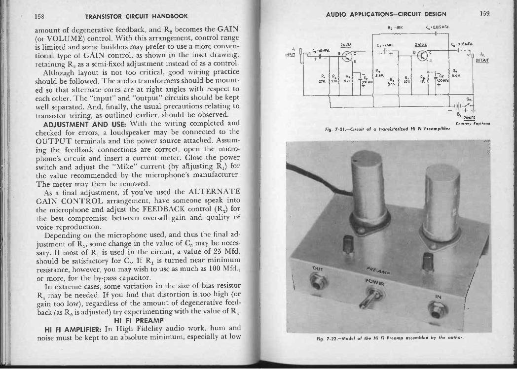
158 TRANSISTOR CIRCUIT HANDBOOK AUDIO APPLICATIONS-CIRCUIT DESIGN 159
amount of degenerative feedback, and R9 becomes the GAIN(or VOLUME) control. With this arrangement, control rangeis limited and some builders may prefer to use a more conven-tional type of GAIN control, as shown in the inset drawing,retaining R2 as a semi -fixed adjustment instead of as a control.
Although layout is not too critical, good wiring practiceshould be followed. The audio transformers should be mount-ed so that alternate cores are at right angles with respect toeach other. The "input" and "output" circuits should be keptwell separated. And, finally, the usual precautions relating totransistor wiring, as outlined earlier, should be observed.
ADJUSTMENT AND USE: With the wiring completed andchecked for errors, a loudspeaker may be connected to theOUTPUT terminals and the power source attached. Assum-ing the feedback connections are correct, open the micro-phone's circuit and insert a current meter. Close the powerswitch and adjust the "Mike" current (by afljusting R1) forthe value recommended by the microphone's manufacturer.The meter may then be removed.
As a final adjustment, if you've used the ALTERNATEGAIN CONTROL arrangement, have someone speak intothe microphone and adjust the FEEDBACK control (R,,) forthe best compromise between over-all gain and quality ofvoice reproduction.
Depending on the microphone used, and thus the final ad-justment of R1, some change in the value of C5 may be neces-sary. If most of R, is used in the circuit, a value of 25 Mfd.should be satisfactory for C5. If R, is turned near minimumresistance, however, you may wish to use as much as 100 Mfd.,or more, for the by-pass capacitor.
In extreme cases, some variation in the size of bias resistorR4 may be needed. If you find that distortion is too high (orgain too low), regardless of the amount of degenerative feed-back (as R, is adjusted) try experimenting with the value of R4.
HI Fl PREAMPHI Fl AMPLIFIER: In High Fidelity audio work, hum and
noise must be kept to an absolute minimum, especially at low
J,
u t_icoomFd.NPUT- 1 1
R,27K
RZ27K
2N133
R3
8.2K
C
Rs 18K C4 -0.015MFd.
czI300stro
C5 2MF.
-/-
R45.6K
Re82K
21.1132.
8 C
C, -0.05MFd.
OUTPUT
R9Cg
54KR,R810K I K
I300MF-I-
Fig. 7-21.-Circuit of a transistorized Hi Fi Preamplifier
B,POWER
Courtesy Raytheon
Fig. 7-22.-Model of the Hi Fi Preamp assembled by the author.
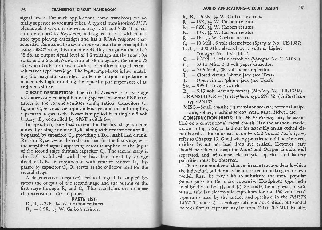
160 TRANSISTOR CIRCUIT HANDBOOK AUDIO APPLICATIONS -CIRCUIT DESIGN 161
signal levels. For such applications, some transistors are ac-tually superior to vacuum tubes. A typical transistorized Hi Fiphongraph Preamp is shown in Figs. 7-21 and 7-22. This cir-cuit, developed by Raytheon, is designed for use with reluct-ance type pick-up cartridges and has a RIAA response char-acteristic. Compared to a twin -triode vacuum tube preamplifierusing a 6SC7 tube, this unit offers 44 db gain against the tube's32 db, an output signal level of 1.6 volts against the tube's 0.4volts, and a Signal Noise ratio of 78 db against the tube's 72db, when both are driven with a 10 millivolt signal from areluctance type cartridge. The input impedance is low, match-ing the magnetic cartridge, while the output impedance ismoderately high, matching the typical input impedance of anaudio amplifier.
CIRCUIT DESCRIPTION: The Hi Fi Preamp is a two -stageresistance -coupled amplifier using special low -noise PNP tran-sistors in the common -emitter configuration. Capacitors C1,C3, and C6 serve as the input, interstage, and output couplingcapacitors, respectively. Power is supplied by a single 6.5 voltbattery, B1, controlled by SPST switch Sw1.
In operation, base bias current for the first stage is deter-mined by voltage divider R1 -R2 along with emitter resistor R3,by-passed by capacitor C2, providing a D.C. stabilized circuit.Resistor R4 serves as the collector load for the first stage, withthe amplified signal appearing across it applied to the inputof the second stage through capacitor C3. The second stage isalso D.C. stabilized, with base bias determined by voltagedivider R6 -R, in conjunction with emitter resistor R3, by-passed by capacitor C5. R9 serves as the collector load for thesecond stage.
A degenerative (negative) feedback signal is coupled be-tween the output of the second stage and the output of thefirst stage through R5 and C4. This establishes the responsecharacteristic of the amplifier.
PARTS LIST:R1, R2 - 27K, 1/2 W. Carbon resistors.R3 - 8.2K, 1/2 W. Carbon resistor.
R4, R9 - 5.6K, V2 W. Carbon resistors.R5 - 18K, 1/2 W. Carbon resistor.Rs - 82K, 1/2 W. Carbon resistor.R, - 10K, 1/2 W. Carbon resistor.R8 - 1K, 1/2 W. Carbon resistor.C1 - 10 Mfd., 6 volt electrolytic (Sprague No. TE-1087).C2, C5 - 300 Mfd. electrolytic, 6 volts or higher
(Sprague No. TVL-1434).C3 -2 Mfd., 6 volt electrolytic (Sprague No. TE-1081).C4 - 0.015 Mfd., 200 volt paper capacitor.C6 - 0.05 Mfd., 200 volt paper capacitor.J1 - Closed circuit 'phone jack (see Text).J2 - Open circuit 'phone jack (see Text).Sw1 - SPST Toggle switch.B1 - 6.15 volt mercury battery (Mallory No. TR-135R).TRANSISTORS-(1) Raytheon type 2N132; (1) Raytheon
type 2N133.MISC.-Small chassis; (2) transistor sockets; terminal strips,
wire, solder, machine screws, nuts, Misc. Hdwe., etc.CONSTRUCTION HINTS: The Hi Fi Preamp may be assem-
bled on a conventional metal chassis, like the author's modelshown in Fig. 7-22, or laid out for assembly on an etched cir-cuit board . . . for information on Printed Circuit Techniques,refer to Chapter 13. Good wiring practice should be observed,neither lay -out nor lead dress are critical. However, careshould be taken to keep the Input and Output circuits wellseparated, and, of course, electrolytic capacitor and batterypolarities must be observed.
There are a number of changes in construction details whichthe individual builder may be interested in making in his ownmodel. First, he may wish to substitute the more popularphono jacks for the more expensive Headphone type jacksused by the author (J1 and J2). Secondly, he may wish to sub-stitute tubular electrolytic capacitors for the 150 volt "can"type units used by the author and specified in the PARTSLIST (C, and C5) . . . voltage rating is not critical, but shouldbe over 6 volts, capacity may be from 250 to 400 Mfd. Finally,

162 TRANSISTOR CIRCUIT HANDBOOK AUDIO APPLICATIONS-CIRCUIT DESIGN 163
he may wish to substitute a zinc -carbon dry battery for themercury battery specified . . . a suitable replacement is aBurgess type Z4.
With the wiring completed and double-checked for errors,a lead may be run from the INPUT jack to the phonograph'scartridge and from the OUTPUT jack to the amplifier withwhich the Hi Fi Preamp is to be used. Be sure to use shieldedcables for these connections. After checking the Preamp'soperation, it should be permanently mounted at some locationnear the record player . . . many builders will prefer to mountit directly in the record player's base, if room is available.
PHONOGRAPH AMPLIFIER: Because of their low power re-quirements, transistors are ideally suited to the design of bat-tery -operated portable entertainment equipment . . . radioreceivers, phonographs, Guitar amplifiers, etc. We'll discusstransistorized radios in a later Chapter; the schematic diagramfor a high quality Phonograph Amplifier is given in Fig. 7-23.This circuit, developed by the Amperex Electronic Corpora-tion, is fully temperature compensated, and is designed to givemaximum performance with only four transistors. Although
R, -330
F-Th
XTM.
PICKUP
- GAIN
R,6.100K
125 .5.6K
R5BZK
0,71
I5K CL
+IL25
100K
R6
TONE 1C I5K 4 R,
.olI1_
1136
+ 11111'11
/3,POWER
TURNTABLE
moToR,
*WC. THERMISTOR MEG COE0
Courtesy Amperex
Fig. 7-23.-Circuit of a high quality transistorized Phonograph Amplifier. This unit mightalso be used as a Guitar or similar "Music" amplifier, or even as a low power P.A. system.
designed primarily for use in a portable record player, theamplifier is also suitable for use as a musical instrument am-plifier if a suitable pick-up is substituted for the phonographcartridge. It might also serve as the audio section of a transis-torized receiver or as a "loudspeaker booster" for a crystal set.
CIRCUIT DESCRIPTION: The Phonograph Amplifier shownin Fig. 7-23 uses four PNP junction transistors . . . two areresistance -coupled as "gain" stages and two are connected as apush-pull Class B power amplifier. Audio power output isapproximately 200 milliwatts under normal operating condi-tions. D.C. operating power is supplied by a single six voltbattery, controlled by switch Sw1.
In operation, the audio signal is obtained from a high out-put crystal or ceramic phonograph cartridge and fed throughmatching resistor R1 to GAIN control R2. Although consider-able signal is lost in R1, this is offset by the high output of thecartridge and the gain of the amplifier. From the GAIN con-trol, the signal is coupled through R4 and C2 to the input of thefirst amplifier stage. Potentiometer R8 and capacitor C, forma simple "losser" type tone control . . . as R3 is reduced invalue, more and more high frequency signals are by-passed tocircuit ground through C1. Stabilized operation of the firststage is assured by the base bias current arrangement, consist-ing of voltage divider R5 -R, and emitter resistor R7, by-passedby capacitor C3.
The amplified audio signal appearing across collector loadresistor R8 is coupled through capacitor C4 to the second stage.This stage, too, is D.C. stabilized by the base bias current cir-cuit . . . in this case consisting of voltage divider R30 -R andemitter resistor R12, by-passed by capacitor C5.
Additional amplification takes place in the second stage.The collector load for this stage is the primary of transformerT1, which serves both to match the output of the gain stage tothe input of the power output stage and to provide the push-pull drive signal needed.
The power output stage consists of a matched pair of tran-sistors operated as Class B push-pull amplifiers, with D.C.
it

161 TRANSISTOR CIRCUIT HANDBOOK AUDIO APPLICATIONS -CIRCUIT DESIGN 165
stabilization assured by a bias network consisting of R9, R15,and thermistor R14. The power stage is matched to the loud-speaker load by transformer T2. Degenerative (negative) feed-back to the input of the second stage is provided to insuredistortionless operation . . . R13 serves to couple the negativefeedback signal from the secondary of T2 back to the earlierstage. PARTS LIST:
Ri - 330K, y2 W. Carbon resistor.- 500K, Carbon potentiometer, Audio Taper
(Centralab B61).R3 - 100K, Carbon potentiometer (Centralab B41).R4, R,, R - 15K, y2 W. Carbon resistors.R, - 82K, /2 W. Carbon resistor.R7 - 1.8K, y2 W. Carbon resistor.R8 - 5.6K, V2 W. Carbon resistor.R9 - 3K, Carbon potentiometer (Centralab B8).R10 - 39K, y2 W. Carbon resistor.R12 - 470 ohm, y2 W. Carbon resistor.R13 - 100K, y2 W. Carbon resistor.
- 75 ohm thermistor (@ 25°C), negative temperaturecoefficient.
R15 - 120 ohm, y2 W. Carbon resistor.C1 - 0.01 Mfd., disc ceramic capacitor
(Centralab No. DD6-103).C2, C3, 25 Mfd., 25 volt electrolytics
(Barco No. P25-25).C, - 80 Mfd., 6 volt electrolytic (Barco No. P6-80).T1 - Transistor driver transformer (Argonne No. AR -109).To - Transistor output transformer
(Argonne No. AR -139).Sw1, Sw, - SPST Toggle or Slide switches.B1 -6 volt battery . . . Burgess No. Z4, Mallory No. TR-
135R, or four Burgess No. 2 flashlight cells in series.PICK-UP - Tone arm with crystal or ceramic cartridge
with high output (0.5 volt or higher output).MOTOR -6 volt D.C. motor and turntable (see CON-
STRUCTION HINTS).
R14
PM SPKR - 6" to 10" PM Loudspeaker, 8 ohm voice coil.TRANSISTORS - (2) Amperex type 0071; Matched pair
Amperex type 0072.MISC. - Small chassis or etched circuit board; (2) control
knobs; Cabinet; Terminal strips; Machine screws, nuts,wire, solder, Misc. Hdwe.
CONSTRUCTION HINTS: The Phonograph Amplifier maybe assembled either on a conventional chassis or on an etchedcircuit board, depending on the individual builder's prefer-ence (for details on Printed Circuits, see Chapter 13). It isnecessary to solder the transistors in place, since these particu-lar units are not well suited to mounting in standard transistorsockets. Observe the usual precautions against overheatingwhen installing the transistors. And, of course, be sure todouble-check electrolytic capacitor and battery polarities.
You may have some slight difficulty locating a phonographturntable and motor combination requiring six volts D.C.-although several have been made for commercial applications,the author knows of no "across -the -counter" sources of suchunits. If you have a machine shop available, and are skilled inmechanical design, you might wish to design and build yourown turntable -motor around one of the commonly availableminiature battery -operated model motors. Or, as an alterna-tive, you might wish to substitute a spring -driven motor andturntable for the electric unit.
Average current drain for the amplifier proper is only about30 milliamperes at 6 volts, or about 0.18 watts (180 milliwatts).Therefore, the total current drain will depend more on thephonograph motor used than on the amplifier. For maximumbattery life, the spring -driven motor -turntable suggested aboveis recommended. If the spring -driven motor is used, either theBurgess Z4 or the Mallory TR-135R batteries may be used. Ifan electric motor is employed, four large (Burgess No. 2) flash-light batteries should be used as a power source . . . the flash-light cells are connected in series and may be mounted in twoAustin -Craft No. 145 Battery Boxes.
After the wiring is completed and double-checked for errors,

166 TRANSISTOR CIRCUIT HANDBOOK
check the connection of feedback resistor R13 to transformerT2. With one connection oscillation may occur, due to positivefeedback. If this happens, reverse the secondary leads (T2).BIAS control R9 should be set about mid -way in its range dur-ing this test. As a final step, R9 is set so that the 0072's drawabout 1.5 milliamperes under "no signal" conditions. Thisshould be between 1000 and 3000 ohms. Use a milliameter(connected between the Red transformer lead of T, and Sw1)to check collector current during this adjustment.
CONCLUSIONThe projects described in this Chapter represent only a
small sampling of the possible applications of transistors toAudio circuits, but they should give the reader a definite"feeling" for the potentialities of these mighty mites. Theauthor hopes the reader will feel encouraged to "carry on"from this point and work up new applications of his own.
In later Chapters additional audio applications will be cov-ered . . . and circuits will be shown for control circuits, codepractice oscillators, toys, and other transistorized devices oper-ating at audio frequencies.
Chapter 8
R.F. APPLICATIONS
Early point -contact transistors could be used at both audioand radio frequencies; not so the early junction units, whichwere suitable for use at audio frequencies only. For a longtime, the expressions "R.F. Transistor" and "Point -ContactTransistor" were almost interchangeable. However, with im-provements in design, modifications in construction, and re-finements in manufacturing methods, the upper frequencylimit of junction transistors has been extended higher andhigher until, today, units are available which will operate inthe tens of megacycles. In addition, new techniques have pro-duced transistors which are useable at hundreds, and eventhousands, of megacycles. It is reasonably safe to predict thatin the future the upper frequency limit of transistor operationwill continue to be pushed ever higher.
The majority of the projects described in this Chapter arebased on the use of transistors operating at AM BroadcastBand frequencies (550-1500 KC) and lower. In most instances,however, the circuits given will work at higher frequencies ifproper changes are made in the tuned circuit parameters andif a suitable transistor type is employed. The "criteria" forchoosing an R.F. transistor is its alpha cutoff frequency (orbeta cutoff frequency). This is the frequency at which the gainof the transistor is 0.707 of its low frequency value. Most tran-sistors may be used as oscillators at frequencies greater thantheir cutoff frequency, however. In critical circuits, additionalfactors to consider are the base resistance, which should below, and the interelectrode capacities, which should also below.
When working with tuned circuits, the experimenter shouldremember that the transistor, in most configurations, has a/ow input impedance, and only a moderately high output im-
167

168 TRANSISTOR CIRCUIT HANDBOOK
pedance. If connected directly across a parallel resonant cir-cuit, it may cause considerable loading, resulting in poorselectivity and relatively low gain. For best results, it is a goodidea to "tap down" to match the transistor's impedance.
RECEIVERS
SIMPLE RECEIVER: Radio receivers are by far the most popu-lar projects with students, with home builders, and withgadgeteers. Even the more advanced worker will sometimes
ANT. 0
Gloct 0
viii
36:1AVAI *1!1
TUNING LI '"
1N34A
K
2N107
HEADPHONE
-,0Well 51
Fig. 8-1.-Simple transistorized Receiver using a diode detector.
Fig. 8-2.-Overall view of the Simple Receiver.
RF APPLICATIONS-CIRCUITS 169
get the urge to assemble a receiver . . . if for no other purposethan to demonstrate to his family and friends. The transistor-ized receiver shown in Figs. 8-1 and 8-2 is an excellent projectfor the beginner. It is non -critical, inexpensive, and easy toassemble. The average worker should have no difficulty dupli-cating the author's model in a single evening. When used witha good ground and a moderate sized antenna, it is satisfactoryfor reception of most local stations with adequate Headphonevolume. Under favorable conditions, distant stations may bepulled in".
CIRCUIT DESCRIPTION: As can be seen by reference to Fig.8-1, the Simple Receiver consists of little more than a tunedcircuit, a diode detector, and a transistor amplifier. A PNPtransistor is used, connected in the grounded -emitter configu-ration. Power is supplied by a 15 volt "Hearing Aid" battery,B1, controlled by a SPST Toggle switch, Sw1.
In operation, radio signals picked up by the Antenna -Ground system are selected by a tuned circuit made up ofvariable tuning capacitor C1 and high Q coil L1. A tap is pro-vided on the coil to match the high -impedance tuned circuitto the comparatively low input impedance of the detector -amplifier circuit. The selected R.F. signal supplied from thetap on L1 is fed to the detector, consisting of a 1N34A diodeand the base -emitter circuit of the 2N107 transistor. Theaudio portion of the detected signal is amplified by the tran-sistor and used to drive the Headphone, which serves as thecollector load impedance for the transistor.
PARTS LIST:CI - 365 Mmf. variable capacitor.L1 - Transistor antenna coil (Lafayette No. MS -166).Sw, SPST Toggle switch.B1 - 15 Volt Hearing Aid battery (Burgess No. Y10).Diode - 1N34A germanium diode.Transistor - (1) GE type 2N107.MISC. - (1) transistor socket; (4) binding posts; Battery
box (Austin -Craft No. 136); Control knob; High impe-
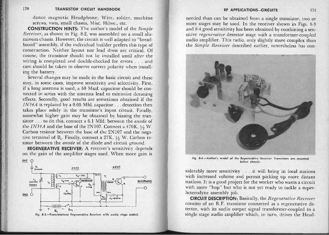
170 TRANSISTOR CIRCUIT HANDBOOK RF APPLICATIONS-CIRCUITS 171
dance magnetic Headphone; Wire, solder, machinescrews, nuts, small chassis, Misc. Hdwe., etc.
CONSTRUCTION HINTS: The author's model of the SimpleReceiver, as shown in Fig. 8-2, was assembled on a small alu-minum chassis. However, the circuit is well adapted to "bread-board" assembly, if the individual builder prefers this type ofconstruction. Neither layout nor lead dress are critical. Ofcourse, the transistor should not be installed until after thewiring is completed and double-checked for errors . . . andcare should be taken to observe correct polarity when install-ing the battery.
Several changes may be made in the basic circuit and thesemay, in some cases, improve sensitivity and selectivity. First,if a long antenna is used, a 50 Mmf. capacitor should be con-nected in series with the antenna lead to minimize detuningeffects. Secondly, good results are sometimes obtained if the1N34A is replaced by a 0.05 Mfd. capacitor . . . detection thentakes place solely in the transistor's input circuit. Finally,somewhat higher gain may be obtained by biasing the tran-sistor . . . to do this, connect a 0.1 Mfd. between the anode ofthe 1N34A and the base of the 2N107. Connect a 470K, I/2 W.Carbon resistor between the base of the 2N107 and the nega-tive terminal of B1. Finally, connect a 27K, V2 W. Carbon re-sistor between the anode of the diode and circuit ground.
REGENERATIVE RECEIVER: A receiver's sensitivity dependson the gain of the amplifier stages used. When more gain is
2N135
1111111111 sw+
28107
Fig. 8-3.-Transistorized Regenerative Receiver with audio stage added.
needed than can be obtained from a single transistor, two ormore stages may be used. In the receiver shown in Figs. 8-3and 8-4 good sensitivity has been obtained by combining a sen-sitive regenerative detector stage with a transformer -coupledaudio amplifier. This radio, only slightly more complex thanthe Simple Receiver described earlier, nevertheless has con -
Fig. 8-4.-Author's model of he Regenerative Receiver. Transisors are mountedbelow chassis.
siderably more sensitivity . . . it will bring in local stationswith increased volume and permit picking up more distantstations. It is a good project for the worker who wants a circuitwith more "hop" but who is not yet ready to tackle a super-heterodyne assembly job.
CIRCUIT DESCRIPTION: Basically, the Regenerative Receiverconsists of an R.F. transistor connected as a regenerative de-tector, with its audio output signal transformer -coupled to asingle stage audio amplifier which, in turn, drives the Head-
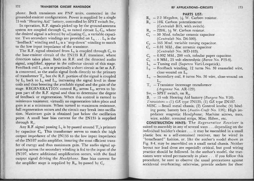
172 TRANSISTOR CIRCUIT HANDBOOK RF APPLICATIONS -CIRCUITS 173
phone. Both transistors are PNP units, connected in thegrounded -emitter configuration. Power is supplied by a single15 volt "Hearing Aid" battery, controlled by SPST switch Sw1.
In operation, R.F. signals picked up by the ground -antennasystem are coupled through C1 to tuned circuit L1 -C2, wherethe desired signal is selected by adjusting C2, a variable capaci-tor. Two secondary windings are provided on L, . . . L2 is the"feedback" winding and L3 is a "step-down" winding to matchto the low input impedance of the transistor.
The R.F. signal obtained from L3 is coupled through C3 tothe base -emitter circuit of the 2N135 R.F. transistor, wheredetection takes place. Both an R.F. and the detected audiosignal, amplified, appear in the collector circuit of this stage.Feedback coil L2 acts as practically a short circuit as far as A.F.is concerned, so the audio signal feeds directly to the primaryof transformer T1, but the R.F. portion of the signal is coupledby L2 back to L1 and L3, increasing the signal level in thesecoils and thus boosting the available signal and the gain of thestage. REGENERATION control R2, across L.>, serves to by-pass part of the R.F. signal and thus to determine the degreeof feedback or regeneration. When this control is turned tominimum resistance, virtually no regeneration takes place andgain is at a minimum. When turned to maximum resistance,full regeneration occurs and the circuit may break into oscilla-tion. Maximum gain is obtained just below the oscillationpoint. A small base bias current for the 2N135 is suppliedthrough R1.
Any R.F. signal passing L2 is by-passed around T1's primaryby capacitor C4. This transformer serves to match the highoutput impedance of the 2N135 to the low input impedanceof the 2N107 audio amplifier, insuring the most efficient trans-fer of energy and thus maximum gain. The audio signal ap-pearing across the secondary winding is fed to the input of the2N107, where additional amplification occurs, with the finaloutput signal driving the Headphone. Base bias current forthe amplifier stage is supplied by R3, by-passed by C5.
PARTS LIST:R1 - 2.2 Megohm, 1/2 W. Carbon resistor.R2 - 10K Carbon potentiometer
(Centralab B15, with switch).- 220K, 1/2 W. Carbon resistor.- 50 Mmf. tubular ceramic capacitor
(Centralab No. D6-500).C2 - 365 Mmf. variable tuning capacitor.C3 - 0.01 Mfd., disc ceramic capacitor
(Centralab No. MD -103).C4 - 0.002 Mfd., 200 volt, tubular paper capacitor.C5 -8 Mfd., 25 volt electrolytic (Barco No. P25-8).L1 - Tuning coil (Superex Vari-Loopstick).L2 - Feedback winding, 12 turns No. 30 enameled wire,
close -wound on L1.L3 - Secondary coil, 8 turns No. 30 wire, close -wound on
L1.T1 - Transistor interstage transformer
(Argonne No. AR -129).Sw1 SPST switch, on R,.B1 - 15 volt Hearing Aid battery (Burgess No. Y10).Transistors - (1) GE type 2N135; (1) GE type 2N107.MISC. - Small metal chassis; (2) Control knobs; (4) bind-
ing posts; battery box (Austin -Craft No. 136); High im-pedance magnetic Headphone; Machine screws, nuts,wire, solder, terminal strips, Misc. Hdwe., etc.
CONSTRUCTION HINTS: The Regenerative Receiver issuited to assembly in any of several ways . . . depending on theindividual builder's choice . . . it may be assembled in a smallplastic box as a self-contained receiver, may be wired in"breadboard" fashion, or, like the author's model shown inFig. 8-4, may be assembled on a small metal chassis. Neitherlayout nor lead dress are especially critical, but good wiringpractice should be followed. In the author's model, the tran-sistors were wired permanently in place . . . if you follow thisprocedure, be sure to observe the usual precautions againstaccidental overheating; otherwise, provide sockets for these
R3C1

174 TRANSISTOR CIRCUIT HANDBOOK
components. Do not install the battery until all wiring is com-pleted and double-checked for accuracy . . . and make sureboth battery and electrolytic capacitor (CO polarities areobserved.
The connections to feedback winding L2 are critical . .
with one connection, the feedback signal will tend to cancelthe original signal, resulting in a loss of gain. If trouble is en-countered, try reversing the lead connections to this coil.
Although the circuit is non -critical, maximum performancecan be obtained by adjusting the bias currents to give opti-mum performance with the individual transistors used. Tochange the bias current values, adjust the sizes of R, (for the2N135) and R3 (for the 2N107).
To use the Regenerative Receiver, connect a good groundto the GND. terminal and an antenna to the ANT. terminal.Connect a high impedance magnetic headset to the HEAD-PHONE terminals and turn up the REGENERATION con-trol, closing switch Sw1. Adjust R2 near its maximum resist-ance value . . . if an audio tone or "putt -putt" sound is heardin the Headphone, turn back R2 until this sound just dis-appears. Finally, adjust TUNING control C2 to pick up thedesired station . . . tune slowly, as the setting may be critical.Readjust R2, "if necessary", as C2 is adjusted and as stations arereceived.
POCKET RECEIVER: Because of their small size, transistorsare ideally suited to the design of miniaturized equipment,
EIND.
ANT.
C.,- UMW
liltZ. lit
ca. _A III363IntAF
L.,
7, LI
IN34A21434 2N35
EARPHONE
OUTPUT
B,
Fig. 8-5.-Schematic diagram of a Pocket Receiver using a two -stagecomplementary amplifier.
%.1
RF APPLICATIONS-CIRCUITS 175
but no attempt has been made to miniaturize the design of theradio receivers described thus far in this Chapter. However, askilled worker, using standard, commercially available compo-nents can assemble a moderate gain transistorized receiver ina box smaller than a package of cigarettes! Such a Pocket Re-ceiver is shown in Fig. 8-6, while the schematic circuit diagram
Fig. 8-6.-Exterior view of the Pocket Receiver . . . assembled in a small plastic box!
is given in Fig. 8-5 and an interior view of the model in Fig.8-7. This tiny receiver operates from its own self-containedbattery and drives a small magnetic earset. While an externalantenna and ground are needed for best reception, strongnearby stations can sometimes be received directly.

176 TRANSISTOR CIRCUIT HANDBOOK RF APPLICATIONS -CIRCUITS 177
Fig. 8-7.-Interior view of the Pocket Receiver.
CIRCUIT DESCRIPTION: Referring to Fig. 8-5, we see thatthe Pocket Receiver consists of a tuned circuit, a diode detec-tor, and a two -stage complementary amplifier, using both PNPand NPN transistors. The common -emitter configuration isused in the amplifier stages. Power is supplied by a small 15volt Hearing Aid battery, controlled by a SPST switch Sw1.The output drives a high impedance magnetic earphone.
In operation, radio signals picked up by the antenna -groundsystem are coupled through C1 to tuned circuit L1 -C2 wherethe desired station is selected by adjusting variable capacitorC2. Secondary winding L2, on L1, couples R.F. energy to the1N34A diode detector and serves to match the low input im-pedance of the detector -amplifier stage, minimizing loading ofthe L1 -C2 tuned circuit, and thus insuring good gain and rea-sonable selectivity.
The detected audio signal, in the base -emitter circuit of thefirst stage, a 2N34 PNP transistor, is amplified by this stageand direct -coupled through R1 to the base -emitter circuit of
the second stage, a 2N35 NPN transistor. R1 serves simply tolimit base current flow in the second stage and thus to protectthe transistors against overloads on strong stations . . . it is nototherwise essential to circuit operation. Further amplificationoccurs in the second stage, with the output audio signal usedto drive a high impedance magnetic earphone, connected toOUTPUT jack L.
PARTS LIST:R, - 2.2K, 1/2 W. Carbon resistor.C1 - 50 Mmf. tubular ceramic capacitor
(Centralab No. D6-500).C2 - Miniature tuning capacitor, 365 Mmf.
(Lafayette No. MS -215).L1 - R.F. Antenna coil
(Superex Ferri-Loopstick cut down).L2 - Approx. 15-20 turns No. 30 enameled wire on L1.B1 - 15 Volt Hearing Aid battery (Eveready No. 504ER).Sw1 SPST switch (see CONSTRUCTION HINTS).Diode - 1N34A germanium diode.Transistors - (1) Sylvania type 2N34; (1) Sylvania type
2N35.MISC. - Open circuit jack, J1 (Telex No. 9240); High im-
pedance magnetic earphone (Argonne No. AR50); Mini-ature 'phone plug (Telex No. 9231); (2) transistor sock-ets; control knob; small plastic case; Machine screws;nuts, wire, solder, Misc. Hdwe., etc.
CONSTRUCTION HINTS: While neither circuit layout norlead dress are critical, some care must be exercised in assem-bling and wiring the Pocket Receiver if the small size of theauthor's model is to be retained. Make up a "mock" layout ortwo before drilling holes in the plastic case or attempting tomount components.
The layout and construction used by the author is clearlyevident in the exterior and interior photos of his model, givenin Figs. 8-6 and 8-7, respectively. The 15 volt battery is heldfirmly against the plastic case by a small "L" bracket; the twotransistor sockets are mounted on another small bracket, cut

178 TRANSISTOR CIRCUIT HANDBOOK RF APPLICATIONS-CIRCUITS 179
from a scrap piece of thin aluminum. Both the battery andsocket brackets are held in place by a single machine screwand nut. Simple "Lap" joints were used for soldering all con-nections.
The SPST switch, Swi, consists of a small machine screw, asmall coil spring, and a hex nut. A lead is soldered directly to
C.401,1
ANT 0 F-1
etax0
3
a
Carboy ova3 ®- Ly 1Crt5101.
es IR, 4*
+1Cr nava
0111PVT
C. -0.011111M, 4
Fig. 8-8.-Diagram of a Hi Fi AM Tuner featuring a transistorized preamplifier.
Fig. 8-9.-Exterior view of the Hi Fi Tuner in its cabinet.
Fig. 8-10.-Rear view of the Hi Fi Tuner's chassis.
the nut. In operation, depressing and releasing the screw givesa "push-button" action, while a permanent closure can bemade by turning the screw in until it bears against the positiveterminal of the battery. Switch construction is clearly shownin Fig. 8-7.
HI Fl AM TUNER: High Fidelity enthusiasts or audiophilesare naturally interested in how transistors may be applied totheir pet hobby. In Chapter 7, we discussed the circuit of a

180 TRANSISTOR CIRCUIT HANDBOOK RF APPLICATIONS -CIRCUITS 181
Hi Fi Phonograph Preamplifier (Figs. 7-21 and 7-22). A tran-sistorized Hi Fi Tuner covering the AM Broadcast Band isshown in Figs. 8-8, 8-9 and 8-10. When used with a high qual-ity audio amplifier and loudspeaker, and conected to a goodAntenna -Ground system, this tuner will give results thatshould please even a discriminating "Golden Ear". In additionto its ability to deliver a high quality audio signal, the Hi FiAM Tuner is free of the hum and noise often associated withA.C. line operated equipment, for, being transistorized andbattery -powered, it is completely independent of power lineconnections.
CIRCUIT DESCRIPTION: The Hi Fi Tuner consists of a broadband, but selective, R.F. tuned circuit, a diode detector, anda two -stage resistance -coupled transistor amplifier, featuringPNP transistors connected in the grounded -emitter configura-tion. Power is supplied by a single 6 volt battery, controlledby SPST switch Sw1, mounted on the GAIN (VOLUME) con-trol, R2. Due to the small power requirements of the tran-sistors, battery life should be quite long under normal oper-ating conditions.
Refer to Fig. 8-8. In operation, R.F. signals picked up bythe Antenna -Ground system are fed directly into the primaryof transformer L3. R.F. transformers L1 and L2, coil L3, tuningcapacitors C3 and C4, and coupling capacitors C1, C2 and C3form a double -tuned bandpass tuning arrangement whichserves to select the desired station. Although this circuit has abandwidth of 25 KC at the 2 db points, it is able to selectadjacent stations without difficulty, because of the high Q ofthe coils specified.
The selected radio signal is detected by the CK705 diode,with the audio signal appearing across diode load resistor R1.Capacitor C. serves to by-pass any R.F. remaining after detec-tion. From here the audio signal is coupled through capacitorC7 to the GAIN (VOLUME) control, consisting of fixed re-sistor R3 and potentiometer R0.
A portion of the available audio signal, depending on thesetting of Ro, is coupled through Cs to the base -emitter circuit
of the first amplifier stage. Base bias current for the first stageis supplied through resistor R4. Amplification takes place inthe first stage, with the audio signal appearing across collectorload resistor R5 coupled through capacitor C9 to the input ofthe second stage. Additional amplification takes place in thesecond stage, with the output signal, appearing across collectorload resistor R7, coupled through C1, to OUTPUT jack J1.Bias current for the second stage is supplied by base resistorRs.
PARTS LIST:(1) MILLER No. 585 Tuner Kit, including the following
components:L1, L2 - T.R.F. Ant. coils (Miller No. 242-A).L3 - Mutual coupling coil (Miller No. EL -55).C1, C2 - Coupling capacitors (included in coils L1 and L2).C3, C4 -2 -Gang tuning capacitor, 365 Mmf. each.J1 - Phono type jack (OUTPUT).Plus hardware items . . . including the following:
(1) 2 -Terminal screw -type ANT.-GND. terminal strip.(1) Chassis, 7"x5"x11/2" (Miller No. 855-1).(1) Slide rule dial assembly (Miller No. 152-H).Assorted mounting hardware, screws, nuts, etc.
In addition to the MILLER kit, the following items areneeded:
R1 - 100K, 1/2 W. Carbon resistor.R2 15K Carbon Potentiometer, Audio Taper
(Centralab B20), with switch.R3 - 47K, y, W. Carbon resistor.R4 - 330K, V2 W. Carbon resistor.R5 - 10K, //2 W. Carbon resistor.R6 - 390K, 1/2 W. Carbon resistor.R7 - 6.8K, 1/2 W. Carbon resistor.C5 - 0.015 Mfd., 200 volt tubular paper capacitor.C6 - 500 Mmf., tubular ceramic capacitor
(Centralab No. MD -501).C7, C8 - 25 Mfd., 6 volt electrolytics (Barco No. P6-25).C9 -5 Mfd., 8 volt electrolytic (Barco No. PS8-5).

182 TRANSISTOR CIRCUIT HANDBOOK RF APPLICATIONS-CIRCUITS 183
C10 - 0.05 Mfd., 200 volt, tubular paper capacitor.Sw1 - SPST switch, on R,.B1 -6 volt battery (Burgess No. Z4).Diode -- Raytheon type CK705.Transistors - (2) Raytheon type CK722.MISC. - (2) Control knobs; Cabinet (Bud No. C-1789);
Battery box; Ground lugs, machine screws, nuts, wire,solder, terminal strips, other Misc. hdwe.
CONSTRUCTION HINTS: With a moderate amount of carein assembly, even a builder of limited experience can assemblea Hi Fi Tuner which equals the author's model (shown inFigs. 8-9 and 8-10) and thus rivals professional "factory -built"equipment in appearance. Neither parts layout nor lead dressare especially critical but, of course, good wiring practiceshould be followed.
Machine work is minimized by the pre -drilled and punchedchassis furnished as part of the MILLER kit specified in thePARTS LIST, although not eliminated altogether. The basicMILLER kit is made up as a crystal receiver and thus thereis no provision, on the chassis, for the transistorized audio am-plifier. A few additional holes will be needed for this circuit. . . or, if you prefer, you can employ the technique used bythe author. He assembled the entire transistor amplifier on asmall "sub -chassis" and mounted it, in turn, under the maintuner chassis.
The transistors may be wired permanently in place or in-stalled in the common "in -line" subminiature sockets. If sold-ered in place, the usual precautions to avoid overheatingshould be observed. In any case, the battery should not be in-stalled until after all wiring is completed and double-checkedfor possible errors. Be sure to observe battery and electrolyticcapacitor polarities.
With the wiring completed and checked, install the battery,the transistors, and connect an ANTENNA and GROUNDto the proper terminals. Use a shielded cable to connect theHi Fi Tuner's output to your audio system. Next, with thetuning capacitor plates fully meshed, adjust the dial pointer
to the extreme low frequency end of the dial. Now, tune tothe high frequency end of the dial, picking up a station some-where from 1200 to 1600 KC. Check the dial reading wherethe station is tuned to see if it corresponds with station'sknown operating frequency.
If dial reading does not correspond with station frequency,readjust the small trimmer capacitors on the sides of C3 andC, . . . both at the same time . . . using an insulated alignmenttool. Recheck the dial reading, and keep adjusting until dialreading corresponds with station frequency. The Hi Fi Tuneris then aligned and ready for use . . . you can install it in thecabinet specified in the PARTS LIST or one of your ownchoosing.
SUPERHETERODYNE RECEIVER: If a High Fidelity system isconsidered the "Queen" of audio amplifiers, then the "super -het" receiver must certainly be considered the "King" of radioreceivers, for this general type of circuit offers the maximumin gain and selectivity combined with ease of operation andreliability. The circuit for a simplified four -transistor superhetis given in Fig. 8-11. This particular receiver covers the AMBroadcast Band (500-1500 KC) and uses commercially avail-able components. It has been designed primarily for ease in
T# T cl(TO6A
C
1,
_2 -2-r-
11
0062 L j
C. 01
24-23K .0.
n,
Ts.,
2
0#122
T -
Fig. 8-11.-Schematic diagram of a four -transistor Superheterodyne Receiver.
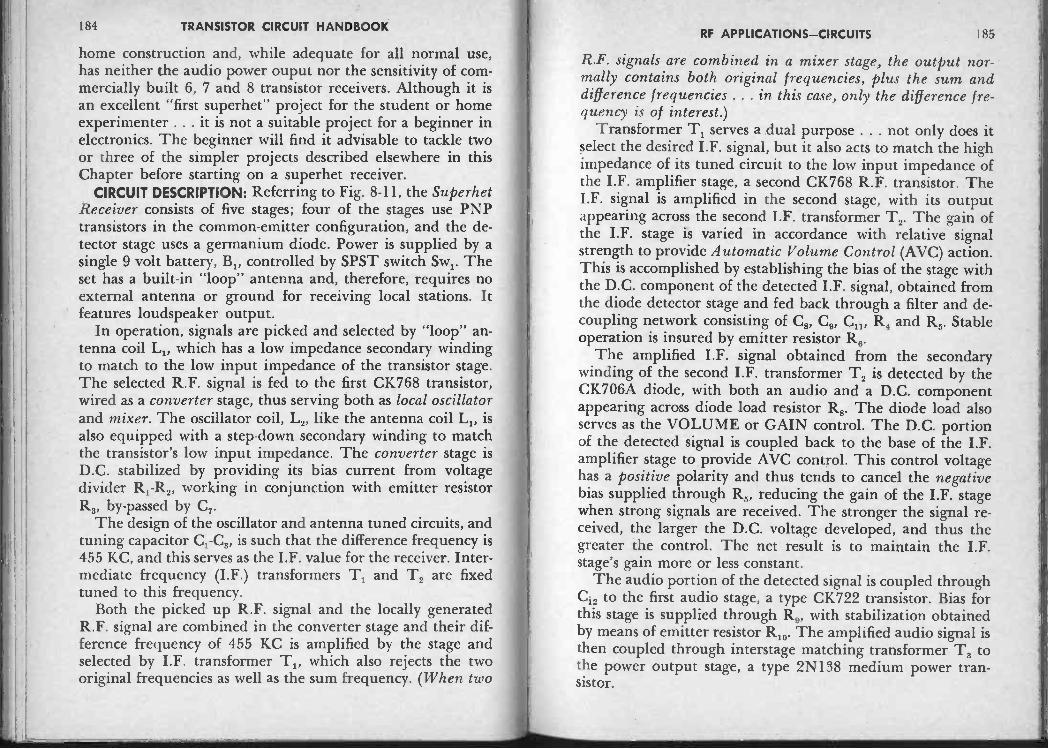
184 TRANSISTOR CIRCUIT HANDBOOKRF APPLICATIONS -CIRCUITS 185
home construction and, while adequate for all normal use,has neither the audio power ouput nor the sensitivity of com-mercially built 6, 7 and 8 transistor receivers. Although it isan excellent "first superhet" project for the student or homeexperimenter . . . it is not a suitable project for a beginner inelectronics. The beginner will find it advisable to tackle twoor three of the simpler projects described elsewhere in thisChapter before starting on a superhet receiver.
CIRCUIT DESCRIPTION: Referring to Fig. 8-11, the SuperhetReceiver consists of five stages; four of the stages use PNPtransistors in the common -emitter configuration, and the de-tector stage uses a germanium diode. Power is supplied by asingle 9 volt battery, B1, controlled by SPST switch Sw1. Theset has a built-in "loop" antenna and, therefore, requires noexternal antenna or ground for receiving local stations. Itfeatures loudspeaker output.
In operation, signals are picked and selected by "loop" an-tenna coil L1, which has a low impedance secondary windingto match to the low input impedance of the transistor stage.The selected R.F. signal is fed to the first CK768 transistor,wired as a converter stage, thus serving both as local oscillatorand mixer. The oscillator coil, L2, like the antenna coil L1, isalso equipped with a step-down secondary winding to matchthe transistor's low input impedance. The converter stage isD.C. stabilized by providing its bias current from voltagedivider R1 -R2, working in conjunction with emitter resistorR3, by-passed by C7.
The design of the oscillator and antenna tuned circuits, andtuning capacitor C1 -C3, is such that the difference frequency is455 KC, and this serves as the I.F. value for the receiver. Inter-mediate frequency (I.F.) transformers T1 and T2 are fixedtuned to this frequency.
Both the picked up R.F. signal and the locally generatedR.F. signal are combined in the converter stage and their dif-ference frequency of 455 KC is amplified by the stage andselected by I.F. transformer T1, which also rejects the twooriginal frequencies as well as the sum frequency. (When two
R.F. signals are combined in a mixer stage, the output nor-mally contains both original frequencies, plus the sum anddifference frequencies . . . in this case, only the difference fre-quency is of interest.)
Transformer T1 serves a dual purpose . . . not only does itselect the desired I.F. signal, but it also acts to match the highimpedance of its tuned circuit to the low input impedance ofthe I.F. amplifier stage, a second CK768 R.F. transistor. TheI.F. signal is amplified in the second stage, with its outputappearing across the second I.F. transformer T2. The gain ofthe I.F. stage is varied in accordance with relative signalstrength to provide Automatic Volume Control (AVC) action.This is accomplished by establishing the bias of the stage withthe D.C. component of the detected I.F. signal, obtained fromthe diode detector stage and fed back through a filter and de -coupling network consisting of C8, C9, C11, R4 and R5. Stableoperation is insured by emitter resistor R6.
The amplified I.F. signal obtained from the secondarywinding of the second I.F. transformer T2 is detected by theCK706A diode, with both an audio and a D.C. componentappearing across diode load resistor R8. The diode load alsoserves as the VOLUME or GAIN control. The D.C. portionof the detected signal is coupled back to the base of the I.F.amplifier stage to provide AVC control. This control voltagehas a positive polarity and thus tends to cancel the negativebias supplied through R5, reducing the gain of the I.F. stagewhen strong signals are received. The stronger the signal re-ceived, the larger the D.C. voltage developed, and thus thegreater the control. The net result is to maintain the I.F.stage's gain more or less constant.
The audio portion of the detected signal is coupled throughC12 to the first audio stage, a type CK722 transistor. Bias forthis stage is supplied through R9, with stabilization obtainedby means of emitter resistor R10. The amplified audio signal isthen coupled through interstage matching transformer T3 tothe power output stage, a type 2N138 medium power tran-sistor.
186 TRANSISTOR CIRCUIT HANDBOOK
Additional gain is obtained from the output stage, with thefinal audio signal coupled to the PM loudspeaker throughoutput transformer T4. The power output stage is stabilizedby means of emitter resistor R13 and the voltage divider net-work used to supply base bias current . . . R and R12, with
R12 by-passed by C13. Capacitor C14, from the 2N138's collectorto ground, serves to by-pass higher frequency signals and thusto reduce the effect of harmonic distortion.
PARTS LIST:
R1, R5 - 100K, V2 W. Carbon resistors.R2 27K, y2 W. Carbon resistor.R3 - 1K, y2 W. Carbon resistor.
- 3.3K, y2 W. Carbon resistor.R6 - 330 ohm, 1/2 W. Carbon resistor.R7, R - 4.7K, y2 W. Carbon resistor.R. - 15K Carbon potentiometer, Audio Taper
(Centralab B20).R9 - 220K, y2 W. Carbon resistor.R10 - 47 ohm, y2 W. Carbon resistor.R12 470 ohm, y2 W. Carbon resistor.R13 - 100 ohm, y2 W. Carbon resistor.C1, C3 Subminiature dual superhet tuning capacitor
(Argonne No. AR -93).C2, C4 Trimmer capacitors . . . part of C1 -C3.
C5, CO, C9, C10, C11, C14 - 0.01 Mfd. Disc ceramics(Centralab MD -103).
C7 0.005 Mfd. Disc ceramic (Centralab MD -502).Cs, C13 - 10 Mfd., 12 volt electrolytic
(Sprague No. TE-1128).C12 -2 Mfd., 6 volt electrolytic (Sprague No. TE-1081).C15 - 25 Mfd., 10 volt electrolytic (Sprague No. TE-1118).L, - "Loop" Antenna coil (Argonne No. AR -97).
- Superhet Oscillator coil (Argonne No. AR -98).Ti, T2- I.F. Transformers, 455 KC (Argonne No. AR -60).T3 - Transistor interstage transformer, 20K to 1K
(Argonne No. AR -104).
RF APPLICATIONS -CIRCUITS 187
T, - Output transformer 400 ohms to 11 ohms(Argonne No. AR -120).
SPKR - Miniature PM Loudspeaker, 10 ohm V.C.(Argonne No. AR -95).
Sw1 - SPST Switch, on R8.B1 -9 volt battery (RCA No. VS300).Diode - (1) Raytheon type CK706A.Transistors - (2) Raytheon type CK768; (1) Raytheon type
CK722; (1) Raytheon type 2N138.MISC. - (4) transistor sockets; battery clips; (2) control
knobs; plastic case or cabinet; terminal strips; Machinescrews, nuts, wire, solder, Misc. Hdwe., etc.
CONSTRUCTION HINTS: While parts layout and wiring leaddress are not especially critical, the builder should exercisecare in laying out the receiver if trouble is to be avoided inmechanical assembly and electrical operation, The accepted"rules" of good wiring practice should be observed . . . thatis signal leads should be kept reasonably short and direct,"input" and "output" circuits of each stage should be keptwell separated, and exposed leads should be protected withinsulating spaghetti tubing.
The 4 -transistor Superhet Receiver is suited to either con-ventional metal chassis construction or to assembly on anetched circuit board, depending on the individual builder'spreference. For information on Printed Circuit Techniquesrefer to Chapter 13. However, regardless of whether conven-tional construction or etched circuitry is employed, the finalreceiver should be housed in a plastic or wooden case (cabinet),for a metal case will tend to shield the "loop" antenna coil L1.
Although the transistors specified in the PARTS LIST areequipped with wire leads suitable for permanent solderinginto the circuit, the author recommends the use of sockets,with the transistor leads cut off to an appropriate length. Theadvantages are two -fold . . . there is less chance of heat damageto the transistors since they are installed after wiring is com-pleted and checked, and, secondly, the builder can experimentwith different transistors. Although the circuit is non -critical

188 TRANSISTOR CIRCUIT HANDBOOK RF APPLICATIONS -CIRCUITS 189
and should not require "selected" transistors for operation, itis an accepted fact that maximum performance of a transistorcircuit may be obtained with selected units.
Once the wiring is completed, re -check the circuit for pos-sible wiring errors or accidental shorts before installing thetransistors or the battery. Pay especial attention to the polarityof electrolytic capacitor connections.
The final step is alignment. With the transistors and batteryinstalled, turn the unit "ON" and turn the VOLUME control(R8) to its full volume position. Turn the TUNING control(C1 -C3) until the plates are fully meshed. Loosely couple astandard R.F. Signal Generator to the antenna coil L1 . . .
often, you can do this simply by placing the "hot" Signal Gen-erator lead near this coil. Set the instrument to supply a modu-lated R.F. signal at 455 KC. Next, using the proper type ofinsulated alignment tool, carefully adjust I.F. transformers T1and T2 for maximum signal output . . . use the minimum signalfrom the Signal Generator which will allow you to hear a tonefrom the loudspeaker of the receiver. Reduce the Signal Gen-erator's output during alignment if necessary to keep signallevel to a minimum. This is necessary to avoid AVC action.
With the I.F. transformers peaked, adjust the TUNINGcontrol for minimum capacity and set the Signal Generator at1575 KC. Adjust trimmer capacitors C, and C, (on the back ofthe tuning capacitor) for peak output. Again, use the mini-mum signal level which permits a useable signal from theloudspeaker. If you've used a calibrated dial, C4 may be set tomake the dial reading correspond with actual frequency, whileC, may be used to "peak" the output at about 1500 KC.
If trouble is encountered with the completed model, it mayindicate either an error in wiring or one or more defectiveparts. Oscillation may indicate poor layout in the R.F. andI.F. circuit sections. Distortion may indicate either defectiveparts or the need for readjustment of bias currents in the audiosection . . . resistors R9 and R may be changed to adjust biasin their respective changes. Finally, if the receiver responds tothe I.F. signal, but appears "dead" at R.F. during alignment,
it may indicate that the local oscillator is not functioning . . .
again, check parts and lead connections also try interchangingthe two CK768 transistors.
MIC.
10(1K
Fig. 8-12.-A miniature Wireless Microphone or "Home Broadcaster".
Fig. 8-13.-Exterior of the "Home Broadcaster"-smaller than a package of cigarettes!!

190 TRANSISTOR CIRCUIT HANDBOOK RF APPLICATIONS -CIRCUITS 191
Fig. 8-14.-Inferior view of the "Home Broadcaster".
TRANSMITTERSWIRELESS MICROPHONE: Although smaller than a package
of cigarettes, the instrument shown in Figs. 8-12, 8-13 and 8-14is actually a miniature Home Broadcaster . . . a type of self-contained "Broadcast Station" which an operator can use tobroadcast his voice through any standard AM Broadcast Re-ceiver within its range. It uses standard components and maybe assembled quite easily by a worker of moderate skill. Al-though its range will depend on the receiver with which it isused, the unit is designed to have a maximum range of 8 to15 feet to insure operation well within the legal limits estab-lished by the FCC. It makes an excellent toy for children, andmay also be used for "party fun" at adult get-togethers.
CIRCUIT DESCRIPTION: The Wireless Microphone uses twoPNP transistors in a rather unique series circuit arrangement,although the basic circuit used with both transistors is essen-tially the common -emitter configuration. A type CK760 R.F.transistor is used as an R.F. oscillator; a type CK722 unit asan audio amplifier. Power is supplied by a single 15 volt Hear-ing Aid battery, controlled by a simple SPST push-buttonswitch, Sw1.
Refer to Fig. 8-12. In operation, the CK760 oscillates at aradio frequency determined by tuned circuit C, -L1. The feed-
back necessary to start and sustain oscillation is determined bysecondary coil L2, coupled to L1. Coil L2 serves a triple func-tion . . . it couples to the tuned circuit, it matches the high im-pedance of the tuned circuit to the input impedances of thetransistor, and, by virtue of its tap, it supplies the necessaryfeedback between collector and base electrodes to insure os-cillation. Base bias current for the R.F. oscillator is suppliedthrough resistor R1. Capacitor C3 serves simply as a D.C.blocking capacitor to avoid applying the full supply voltageto the base.
The R.F. oscillator is modulated by varying its emitter cur-rent in accordance with an audio signal. This is accomplishedby the CK722 transistor, which is connected in series with theCK760's emitter electrode and the power supply, B1. TheCK722 thus serves the dual purpose of modulating the R.F.oscillator and acting as an audio amplifier for the signal ob-tained from the low impedance magnetic microphone (MIC.).Base bias current for the CK722 is supplied by R2, by-passedby C. Capacitor C4, connected between the CK760's emitterand circuit "ground", by-passes R.F. signals at this point, in-suring the operation of the CK760 as a common -emitter oscil-lator, but does not affect the audio signal delivered by theCK722.
The modulated R.F. signal is fed through C1 to "output"jack J into which the antenna wire is plugged. This capacitorserves simply to reduce the capacitive loading of the antennaand is not otherwise essential to circuit operation.
PARTS LIST:R, - 27K, V2 W. Carbon resistor.
- 100 K, I/2 W. Carbon resistor.C1 - 50 Mmf., tubular ceramic capacitor
(Centralab D6-500).C, - 150 Mmf. tubular ceramic . . . see text
(Centralab D6-151).C3 - 0.002 Mfd., disc ceramic (Centralab DD -202).C4 - 0.01 Mfd., disc ceramic (Centralab DD -103).

192 TRANSISTOR CIRCUIT HANDBOOK RF APPLICATIONS -CIRCUITS 193
C, - 16 Mfd., 12 volt electrolytic (Barco No. P12-16).L1 - R.F. Antenna coil, cut down
(Superex Ferri-Loopstick).L2 - About 20 turns of No. 30 enameled wire, close -wound
on L1, with tap about 4 or 5 turns from "base" end.J1 - Miniature open circuit jack (Telex No. 9240).PL,- Miniature plug (Telex No. 9231).B1 - 15 volt Hearing Aid battery (Eveready No. ER505E).Sw1 - SPST switch (see text).MIC. - Miniature magnetic microphone
(Shure Bros. No. MC -11).Transistors - (1) Raytheon CK760; (1) Raytheon CK722.MISC. - (2) transistor sockets; small plastic case; Machine
screws, nuts, wire, solder, Misc. Hdwe., etc.CONSTRUCTION HINTS: The construction details of the
author's model of the Wireless Microphone are clearly visiblein the exterior and interior views of the unit, given in Figs.8-13 and 8-14, respectively. Good wiring practice should befollowed, of course, but no special precautions are necessaryin regard to parts layout and lead dress. Since the workingarea is rather confined . . . at least if the builder attempts toduplicate the author's model as far as size is concerned . . . itis suggested that "lap" joints be used for all soldered connec-tions.
Mechanically, the two transistor sockets are mounted in asmall bracket cut from scrap aluminum, and this bracket, to-gether with the small "L" bracket used to hold the battery (B,)in place, are mounted on the plastic case with a single machinescrew and hex nut. The small microphone is held in place bya simple "U" bracket, made from a strip of sheet metal, andtwo machine screws and nuts.
Push-button switch Sw1 is made up from a small machinescrew, a small coil spring which just fits the screw, and a hexnut. The lead connection is made by soldering a flexible wireto the hex nut. This switch is arranged on the side of the plas-tic case, as shown in Fig. 8-14. When depressed, it makes con-tact with one terminal of B, (a wire is soldered to the opposite
terminal of the battery). A "permanent" connection can bemade by turning the screw in, against the pressure of thespring, until firm contact is made with the battery. This switchis thus identical to that described in Chapter 7 (Pocket Re-ceiver).
Coils L1 and L2 deserve some mention. Coil L1 is made upfrom a commercial antenna coil by cutting away all the card-board form except the short portion on which the coil properis wound, retaining only the coil and the iron "slug". If theiron "slug" is tapped, it may be mounted on the plastic casewith a machine screw . . . otherwise, it can be cemented inplace. Coil L1 consists of about 20 turns of fine enameled wire,close -wound right on top of L1, and with a tap about 4 or 5turns from the "base" end . . . or 15 or 16 turns from the endconnected to the transistor's collector electrode.
If you fail to obtain proper operation when you try the com-pleted Wireless Microphone, you may want to experimentwith L2. Moving the tap towards the center will increase feed-back (if you don't get oscillation). In some cases you may wishto increase or decrease the number of turns to obtain optimumoperation with your particular coil and transistor combination.
Several modifications in the basic design are possible, de-pending on the individual builder's inclinations. The "plug-in" type of antenna used in the author's model may be re-placed by a permanently soldered length of hook-up wire,eliminating J1and PL thus reducing cost slightly. Switch Sw1may be replaced with a toggle or slide switch. The microphonemay be replaced with a PM loudspeaker, together with amatching "output" transformer . . . connect the high impe-dance primary winding of the transformer to the transistorand R the low impedance winding to the speaker's voice coilterminals.
With the wiring completed and checked, the transistors maybe installed and the unit tried. Connect the antenna . . . thisshould be from 2 to 5 feet long and may be ordinary hook-upwire. Turn on an AM Broadcast receiver, and, standing closeto the receiver, depress switch Sw, and start counting slowly,

194 TRANSISTOR CIRCUIT HANDBOOK RF APPLICATIONS-CIRCUITS 195
holding the microphone within a few inches of your lips. Withthe receiver's volume turned up, tune slowly over the Broad-cast Band until you pick up your voice.
For proper operation, the tuning of the Wireless Micro-phone should be such that the signal is picked up at a "deadspot" on the Receiver's dial . . . that is, where no station isheard. To change the tuning of the unit, you can slide L,along its core or, for a major shift in frequency, you can re-place C2 with another capacitor. If C2 is made smaller, operat-ing frequency is increased . . . as C, is made larger, frequencyis decreased. Best results are generally obtained when the fre-quency is adjusted near the middle or low frequency end ofthe band . . . below 1000 KC.
ANT.
C1-7
MMF
END.
ZN 135
-220 BI
Fig. 8-15.-Circuit for a Wireless Code Practice Oscillator.
KEY
WIRELESS CODE PRACTICE OSCILLATOR: Prospective ship-board radio operators, "hams", and military communicationsworkers are just a few of the individuals who need to knowthe Radiotelegraph Code. To learn the code, most beginnerswork with audio frequency "Code Practice Oscillators" . . .
instruments which sound an audio tone in a pair of Head -
Fig. 8-16.-Using the Wireless C.P.O.
Fig. 8-17.-Interior view of the Wireless C.P.O.

196 TRANSISTOR CIRCUIT HANDBOOK RF APPLICATIONS -CIRCUITS 197
phones or in a loudspeaker each time a sending key is de-pressed. We'll show and describe transistorized versions ofsuch devices in a later chapter. The code practice oscillator(C.P.O.) shown in Figs. 8-15, 8-16, and 8-17 is not an audiounit and, therefore, uses no Headphones or speaker in its de-sign. Instead, this device permits true "on the air" practicewhen used with a standard Communications Receiver. TheWireless C.P.O. is actually a miniature self-contained CWtransmitter with a limited range . . . no connection to the re-ceiver with which it is used is needed!
CIRCUIT DESCRIPTION: Referring to Fig. 8-15, we see thatthe Wireless C.P.O. uses a single PNP R.F. type transistorconnected as an R.F. oscillator, using the common -emitterconfiguration.
In operation, the frequency is determined by the tuned"tank" circuit L1 -C2. Secondary coil L2, coupled to L1, servesboth to match the input and output impedances of the tran-sistor and to provide the feedback necessary to start and sus-tain oscillation. L2 is connected directly to the transistor'scollector electrode and through capacitor C3 to the base. Basebias current is supplied through resistor R1.
Power is supplied by a single 15 volt Hearing Aid typebattery, controlled by the sending KEY, which is normallyplugged into jack J1. A series resistor, R3, prevents currentsurges which could damage the transistor as the circuit iskeyed rapidly. By-pass capacitor C4, from emitter to circuitground, serves both as a "key -click" filter and to prevent de-generation which R2 might introduce.
The output CW radio signal is coupled to the antenna bind-ing post (ANT.) through capacitor C1, which serves to reducethe loading and detuning effect of the antenna lead. For con-venience in operation, and to minimize possible body capacity
effects, a ground binding post (GND.) is also provided . . . thispermits an external ground to be connected to circuit ground.
PARTS LIST:R1 - 27K, y2 W. Carbon resistor.R, - 220 ohm, y2 W. Carbon resistor.C1 - 25 Mmf. tubular ceramic capacitor.
- Tuning capacitor, tubular ceramic .
100 Mmf.C3 - 0.005 Mfd., disc ceramic (Centralab DD -502).
- 0.1 Mfd., 200 volt paper capacitor.L1 - R.F. Antenna coil (Superex Vari-Loopstick).L2 - 18 turns #30 enameled wire, close -wound on L1, tap
about 4 to 6 turns from end connected to transistor'sbase.
Ji - Open circuit 'phone jack.B1 - 15 Volt Hearing Aid Battery (Eveready No. 411).Transistor- (1) GE type 2N135.MISC. - (2) Binding posts; (1) Small control knob, 3/16"
hole; transistor socket; battery box (Austin -Craft No.134); small plastic box; small piece of perforated bakeliteboard; Hand Key; Machine screws, nuts, wire, solder,Misc. Hdwe., etc.
CONSTRUCTION HINTS: The layout used in the author'smodel is evident in the interior view of the Wireless C.P.O.,given in Fig. 8-17. The individual builder may follow thislayout when assembling his model, or may make up a new oneto suit his own inclinations, as he chooses, for neither layoutnor lead dress is critical. In the author's model, most of thecircuit is assembled on a small piece of perforated bakelitewhich, in turn, is mounted in the plastic box serving as a case.The transistor socket is cemented to the bakelite using GeneralCement No. 45-2 "All -Purpose" Cement; other parts aremounted with small machine screws and hex nuts.
Coil L, is hand -wound on L1, using No. 30 enameled wire.Specifications for this coil are given in the PARTS LIST, butneither the exact number of turns nor the exact location ofthe tap are critical. Some builders may wish to experimentwith this coil to get maximum performance with their tran-sistor.
C2
C4
. . from 50 to

198 TRANSISTOR CIRCUIT HANDBOOK
When wiring is completed and double-checked for possibleerrors, the transistor and battery may be installed and theHand Key connected to jack J1. Place the completed unit nearyour Communications Receiver, as shown in Fig. 8-16. Makesure the Receiver has had time to "warmp up", then turn onits B.F.O. (Beat Frequency Oscillator) . . . the B.F.O. must beused to obtain an audio tone in the speaker, just as if a codesignal from a radio station were being received, for the Wire-less C.P.O. works just like a CW transmitter.
Depress the Hand Key (or close its switch) and try tuningthe receiver over the range from 1000 to 2000 KC. Tune slow-ly and listen for a beat note. When the signal is received, youcan try your hand at sending code!
For best results, the Wireless C.P.O. should be adjusted toan operating frequency slightly above the AM Broadcast Band(above 1600 KC). Its operating frequency may be changed byadjusting Li's iron "slug" or by changing fixed tuning capaci-tor C2. The capacitor may be changed for a "coarse" frequencyadjustment, with the "slug" adjusted for "fine tuning".
When an antenna lead and ground wire are attached to theproper binding posts, the operating frequency may shift slight-ly, requiring retuning of either the Receiver or the WirelessC.P.O. With a moderate length antenna wire and a goodground connection, the device has a transmitting range of 25to 50 feet, when used with the average Communications Re-ceiver.
CRYSTAL CALIBRATOR: A crystal -controlled R.F. oscillator,operating at a frequency of 100 KC and supplying a signalrich in harmonics, can be an extremely valuable tool in theradio -electronics lab. or home electronics workshop. It can beused for such jobs as calibrating the dial of a CommunicationsReceiver or checking the accuracy of an R.F. Signal Genera-tor. Vacuum -tube operated versions of this instrument havebeen available for a number of years, but, like most vacuum -tube devices, they lack the portability, compact size, and easeof use which characterizes transistorized equipment.
R,IK
RF APPLICATIONS -CIRCUITS
Fig. 8-18.-Diagram of a 100 KC crystal -controlled Calibrator.
Fig. 8-19.-Checking the dial calibration of a communications receiver.
I 99

200 TRANSISTOR CIRCUIT HANDBOOK RF APPLICATIONS-CIRCUITS 201
Fig. 8-20.-Interior view of he Crystal Calibrator.
The Crystal Calibrator shown in Figs. 8-18, 8-19 and 8-20 isa reliable and accurate 100 KC oscillator which is completelyself-contained, requiring no power line connection or externalbatteries, yet is housed within a case hardly larger than apackage of cigarettes. It is completely portable and thus idealfor both lab. and field work; and, with only one control andone adjustment, it is extremely easy to use.
CIRCUIT DESCRIPTION: The schematic wiring diagram ofthe Crystal Calibrator is given in Fig. 8-18. This instrumentuses a single NPN transistor in a modified common -base cir-cuit configuration. It is powered by a 15 volt Hearing Aidbattery, controlled by a SPST miniature slide switch (Sw1).
In operation, adjustable choke coil L1 serves as the collectorload impedance and resistor R1 as the emitter load. Feedbackbetween the collector and emitter circuits is provided by acapacitive voltage divider C1 -C2, which also serves as an im-pedance matching network, matching the relatively high im-
pedance of the collector circuit to the low "input" impedanceof the emitter.
The base is "floated" above circuit ground by resistor R2.This resistor would normally introduce enough degenerationto prevent oscillation, but it is "by-passed" by the 100 KCcrystal (XTAL). Since the crystal acts effectively like a seriesresonant circuit, offering a low impedance at its resonant fre-quency, it serves to "short" the base to ground, permitting thetransistor to work as a common -base amplifier at this one fre-quency. Oscillation can then take place due to the feedbacksupplied by the C1 -C2 network. For proper operation, signalphase relationships must be correct, and this is insured bymaking L1 adjustable.
PARTS LIST:R1 - 1K, 1/2 W. Carbon resistor.R, - 27K, 1/2 W. Carbon resistor.C1 - 100 Mmf. tubular ceramic capacitor
(Centralab D6-102).- 50 Mmf. tubular ceramic capacitor (Erie GPIK).
C3 - 270 Mmf. tubular ceramic capacitor(Centralab D6-271).
L1 - 15 MHy adjustable choke coil (Superex No. V-25).Sw1 - SPST slide switch.B1 - 15 Volt Hearing Aid battery (Burgess No. U10).XTAL - 100 KC Quartz Crystal
(Hupp Electronic Corp. Type 44).Transistor - (1) GE type 2N169.MISC. - Transistor socket; battery box (Austin -Craft No.
134); Small plastic box; Machine screws, nuts, wire,solder, Misc. Hdwe., etc.
CONSTRUCTION HINTS: Most workers should have no diffi-culty assembling and wiring the Crystal Calibrator for neitherparts layout nor lead dress are critical. Only standard, readilyavailable components are used. Even when assembled in asmall plastic box, like that used in the author's model, wiringis not crowded and no special skills are required.
Construction details and general layout used by the author
C2

202 TRANSISTOR CIRCUIT HANDBOOK RF APPLICATIONS -CIRCUITS 203
are clear in the exterior and interior views of his model, shownin Figs. 8-19 and 8-20, respectively. In the author's model, allparts were mounted on a small Bakelite "sub -chassis" which,in turn, was mounted in the plastic case. The transistor socketwas cemented in place, other parts were mounted with smallmachine screws and hex nuts. The adjustable coil, L1, wasmounted using a small "L" bracket made up from a scrappiece of aluminum. The antenna (ANT.) is a 20" to 30"length of flexible hook-up wire.
ADJUSTMENT AND USE: Once wiring is completed andchecked, the transistor and battery may be installed. Remem-ber that a NPN transistor is used, and pay especial attentionto battery polarity.
To use the Crystal Calibrator, simply spread out the ANT.lead near your Communications Receiver and close the powerswitch Sw,. For maximum output, the ANT. lead may beconnected directly to the ANTENNA post of the receiver . . .
no ground connection is needed. Coil L1 must be adjustedinitially until oscillation occurs; afterwards, it serves as a"vernier" control on frequency . . . however, since the oper-ating frequency is controlled primarily by the crystal, don'texpect to be able to shift frequency appreciably by adjustingL1!
The Crystal Calibrator supplies a CW (unmodulated) sig-nal. Therefore, to hear its signal in your receiver, you'll haveto turn on the B.F.O. . . . just as if you were receiving codesignals. When both the set and the instrument are on andproperly adjusted, you'll get audio "beat" notes at 100 KCintervals across the dial. The author's model gave strong beatsto 36 MC, the upper frequency limit of his CommunicationsReceiver. When used to check the calibration of a R.F. SignalGenerator, both the Signal Generator and the Crystal Cali-brator are connected to the receiver . . . the B.F.O. is notneeded in this case, for the "beat" note is obtained betweenthe two R.F. signals.
HAM GEARHAM STATION MONITOR: Some amateur radio operators
like to monitor their CW transmissions. One way they can dothis is to tune their Communications Receiver near their sta-tion frequency and to use it as a "Monitor". This system hasseveral drawbacks . . . not only is there a chance of overloadingthe Receiver, due to the close proximity of a powerful signalsource, but two-way communications are more difficult tocarry on, since the Receiver must be retuned to the incomingstation's frequency after each transmission. A simpler andmore satisfactory approach is to assemble a compact StationMonitor . . . the circuit for a transistorized version of such adevice is given in Fig. 8-21. This unit provides an audio notein the Headphones whenever the transmitter is "sending".
vr#PICK-UP
LOOP
C1-(668 TEXT)
47K
I N66
Fig. 8-21.-Schematic of an easily built Ham Station Monitor.
CIRCUIT DESCRIPTION: The Station Monitor is basically atwo -stage complementary oscillator, using direct -coupled PNPand NPN transistors in the common emitter configuration.Power is supplied by R.F. energy obtained from the station'stransmitter, after appropriate rectification and filtering. Sincepower is supplied only when the transmitter is working, theoscillator can operate only at this time, and since only a smallfraction of a watt is needed by the transistorized oscillator,there is no detrimental effect on the station's power output.
In operation, the type 2N107 PNP transistor is direct -coupled to the type 2N170 NPN unit, forming a two -stageamplifier. A pair of magnetic Headphones serves as the collec-tor load impedance for the second stage. Resistor R1 serves as

204 TRANSISTOR CIRCUIT HANDBOOK
the base resistor for the first stage. Since direct -coupling isemployed, the second stage requires no base resistor. CapacitorC1 is connected between the "output" and the "input" of thetwo -stage amplifier to convert it into an audio oscillator . . .
this capacitor serves as the feedback path.R.F. power is picked up by a small loop near the transmitter
and tranferred to the Station Monitor over a simple transmis-sion line. Here, a 1N66 diode is used as a half --wave rectifierwhich, together with filter network 11.2-C2, forms the D.C.power supply for the audio oscillator.
PARTS LIST:R1 - 47K, 1/2 W. Carbon resistor.R, - 470 ohm, 1/2 W. Carbon resistor.C1 - 0.001 to 0.01 Mfd. (see text), ceramic or paper
capacitor.C2 - 0.5 Mfd., 200 volt paper capacitor.LOOP - Approximately 3 turns hook up wire, about 21/2"
to 3" diameter, loosely coupled to the transmitter.Diode - (1) GE type 1N66.Transistors - (1) GE type 2N107 PNP transistor; (1) GE
type 2N170, NPN.MISC. - (2) Transistor sockets; high impedance magnetic
headphone; twisted pair lamp cord; small plastic box;Machine screws, nuts, wire, solder, Misc. Hdwe., etc.
CONSTRUCTION HINTS: The entire Station Monitor maybe assembled in a small plastic or metal box. Good wiringpractice should be observed, but neither layout nor lead dressare critical. The Pick-up Loop consists of about three turns ofinsulated hook up wire, wound on a form about two to threeinches in diameter. It is connected to the Station Monitor witha short length of twisted pair lamp cord and loosely coupledto the transmitter. You may have to experiment to determinethe best location for the pick-up coil.
When assembling the Station Monitor pay particular atten-tion to the polarity of transistor and diode connections. If de-sired, the NPN and PNP units may be interchanged, provided
RF APPLICATIONS -CIRCUITS 205
the diode is reversed to insure proper power supply voltagepolarity.
Capacitor Cl is chosen experimentally to give the audionote desired. Generally, its value should be between 0.001 and0.01 Mfd., but its final value will depend on the audio fre-quency desired and on the impedance of the Headphone used.
Circuit values are not especially critical, but you may find itworthwhile to experiment somewhat, to obtain optimum per-formance with your particular assembly . . . and under yourspecial operating conditions. You can try varying the valuesof R1, R2 and C2.
R.F. FREQUENCY METER: If there is any one instrument thatis found almost universally in "Ham Shacks", it is probablythe Absorption Frequency Meter. Used for quick transmitterfrequency checks, this instrument may take many forms. Inits simplest form it consists of an inductance coil and variablecapacitor, connected as a tuned circuit in series with a smallflashlight bulb which serves as an indicating device. In use,the instrument is held near the transmitter and tuned throughresonance . . . at the resonant frequency the circulating cur-rent, induced by the proximity of the transmitter, reaches amaximum, and the small bulb glows. Such an instrument re-quires a fair amount of power for operation. Some Hams usea more sensitive form, substituting a diode detector and D.C.meter for the lamp bulb indicator . . . these instruments givea peak in meter reading at resonance, and require less powerthan the simpler circuit.
esTONI**
11/LY
Ca -100 UHF
-.0of2.N541
cc.01 MN.
na5K
METERSENSITIVITY
'PHONES
Fig. 8-22.-Circuit for a transistorized R.F. Frequency Meter.

206 TRANSISTOR CIRCUIT HANDBOOK
By combining the detection and D.C. amplifying character-istics of the transistor with the basic circuitry of the absorptionfrequency meter, we can develop an instrument that is moresensitive than either of the simpler forms, yet is still easy toassemble and to use. The circuit for a transistorized R.F. Fre-quency Meter is given in Fig. 8-22, while an exterior view ofthe author's model of the instrument is shown in Fig. 8-23.
Courtesy Radio 8 Television NewsFig. 8-23.-Exterior view of the R.F. Frequency Meter.
CIRCUIT DESCRIPTION: Referring to Fig. 8-22, tuned cir-cuit L1 -C, is used to pick up the R.F. signal to be checked.Normally, pick-up is made by inductive coupling to the coilproper, but provision has been made for the use of an antennaand ground, if desired. A tap on L, matches the low inputimpedance of the PNP transistor and minimizes the loadingeffect of the transistor on the tuned circuit.
RF APPLICATIONS -CIRCUITS 207
The R.F. signal is coupled through C3 to the base -emittercircuit of the transistor, connected in the common -emitterconfiguration and operated without bias current so as to serveas a detector -amplifier. Resistor R, serves as the base resistor.
The collector current of the transistor varies with the ampli-tude of the applied R.F. signal and this current, in turn, isindicated on the meter (M). Thus, the meter reading indicateswhen there is a peak in the tuning of CA, and therefore theresonance of this circuit. The meter is shunted by potentiom-eter R2, which serves as a SENSITIVITY control, and thusprevents possible overloading of the meter on strong signals.The meter is by-passed by capacitor C6, which prevents attenu-ation of the audio signal when a modulated R.F. signal is be-ing received, and when Headphones are plugged into jack J,for monitoring purposes. Capacitors C, and C5 serve as R.F.by-pass capacitors. Power is supplied by a single penlight cell,B,, controlled by SPST toggle switch Sw,.
PARTS LIST:
R, - 10K, 1/2 W. Carbon resistor.- 5K, Carbon potentiometer, Linear Taper
(Centralab B10).C, - Variable capacitor, Tuning
(Hammarlund HF-140 . . . 140 Mmf.).C2 - 100 Mmf., tubular ceramic (Centralab D6-101).C3 - 0.005 Mfd., disc ceramic (Centralab MD -502).C4 - 0.002 Mfd., disc ceramic (Centralab-MD-202).C5 - 0.01 Mfd., disc ceramic (Centralab MD -103).C, - 0.1 Mfd., 200 volt tubular paper capacitor.L, - Tapped inductance coil -see text.B, - 1.5 volt penlight cell (Burgess No. Z).Sw, - SPST toggle switch.J, - Closed circuit 'phone jack.M - Meter, 0-200 Microamperes.Transistor - (1) Transitron type 2N34.MISC. - Transistor socket; control knob; coil socket; (2)
binding posts vernier tuning dial (National AM -2); small
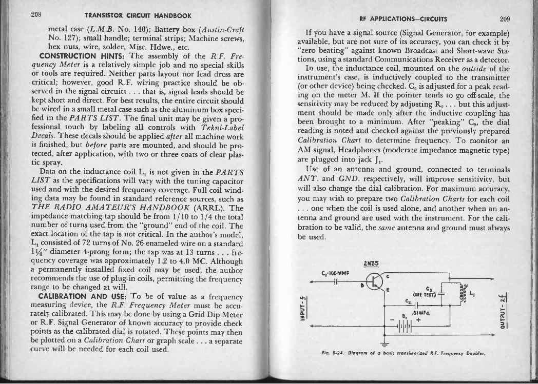
208 TRANSISTOR CIRCUIT HANDBOOK RP APPLICATIONS -CIRCUITS 209
metal case (L.M.B. No. 140); Battery box (Austin -CraftNo. 127); small handle; terminal strips; Machine screws,hex nuts, wire, solder, Misc. Hdwe., etc.
CONSTRUCTION HINTS: The assembly of the R.F. Fre-quency Meter is a relatively simple job and no special skillsor tools are required. Neither parts layout nor lead dress arecritical; however, good R.F. wiring practice should be ob-served in the signal circuits . . . that is, signal leads should bekept short and direct. For best results, the entire circuit shouldbe wired in a small metal case such as the aluminum box speci-fied in the PARTS LIST. The final unit may be given a pro-fessional touch by labeling all controls with Tekni-LabelDecals. These decals should be applied after all machine workis finished, but before parts are mounted, and should be pro-tected, after application, with two or three coats of clear plas-tic spray.
Data on the inductance coil L1 is not given in the PARTSLIST as the specifications will vary with the tuning capacitorused and with the desired frequency coverage. Full coil wind-ing data may be found in standard reference sources, such asTHE RADIO AMATEUR'S HANDBOOK (ARRL). Theimpedance matching tap should be from 1/10 to 1/4 the totalnumber of turns used from the "ground" end of the coil. Theexact location of the tap is not critical. In the author's model,L1 consisted of 72 turns of No. 26 enameled wire on a standard11/4" diameter 4-prong form; the tap was at 13 turns . . . fre-quency coverage was approximately 1.2 to 4.0 MC. Althougha permanently installed fixed coil may be used, the authorrecommends the use of plug-in coils, permitting the frequencyrange to be changed at will.
CALIBRATION AND USE: To be of value as a frequencymeasuring device, the R.F. Frequency Meter must be accu-rately calibrated. This may be done by using a Grid Dip Meteror R.F. Signal Generator of known accuracy to provide checkpoints as the calibrated dial is rotated. These points may thenbe plotted on a Calibration Chart or graph scale . . . a separatecurve will be needed for each coil used.
If you have a signal source (Signal Generator, for example)available, but are not sure of its accuracy, you can check it by"zero beating" against known Broadcast and Short-wave Sta-tions, using a standard Communications Receiver as a detector.
In use, the inductance coil, mounted on the outside of theinstrument's case, is inductively coupled to the transmitter(or other device) being checked. C2 is adjusted for a peak read-ing on the meter M. If the pointer tends to go off -scale, thesensitivity may be reduced by adjusting R, . . . but this adjust-ment should be made only after the inductive coupling hasbeen brought to a minimum. After "peaking" C,, the dialreading is noted and checked against the previously preparedCalibration Chart to determine frequency. To monitor anAM signal, Headphones (moderate impedance magnetic type)are plugged into jack J1.
Use of an antenna and ground, connected to terminalsANT. and GND. respectively, will improve sensitivity, butwill also change the dial calibration. For maximum accuracy,you may wish to prepare two Calibration Charts for each coil. . . one when the coil is used alone, and another when an an-tenna and ground are used with the instrument. For the cali-bration to be valid, the same antenna and ground must alwaysbe used.
2N35
Fig. 8-24.-Diagram of a basic transistorized R.F. Frequency Doubler.
1-

2 I I) TRANSISTOR CIRCUIT HANDBOOK
Fig. 8-25.-Breadboarded Frequency Doubter.
SPECIAL R.F. CIRCUITSFREQUENCY DOUBLER: Where practical considerations
make it difficult to design and build an oscillator to deliver adesired signal frequency, it is common practice to use a Fre-quency Doubler. In its simplest form, this is a non-linear am-plifier which drives a resonant circuit tuned to twice the inputsignal frequency. Transistors are well suited to the design ofsuch devices. The circuit for a transistorized FrequencyDoubler is given in Fig. 8-24, while an assembled "bread-board" model is shown in Fig. 8-25.
CIRCUIT DESCRIPTION: As we can see by referring to Fig.8-24, a single NPN transistor is used in this device, connectedas a tuned amplifier in the common -emitter configuration.Power is supplied by a single battery. Since this is an experi-mental circuit, no controls or switches are provided or needed.
In operation, the input signal is coupled to the base -emitter
RF APPLICATIONS -CIRCUITS 211
circuit through capacitor C1. Since no base resistor is used, thetransistor is operated without bias current and thus acts to"detect" or "clip" the incoming signal, feeding amplifiedpulses to its collector load . . . tuned circuit L1 -C3. Thesepulses "shock -excite" the tuned circuit at its resonant fre-quency, producing an output signal at this value. For fre-quency doubling, resonant circuit 1,1-C3 is tuned to twice thefrequency of the applied signal.
Capacitor C2 serves simply as an R.F. by-pass across thepower source, battery B1, and is not essential to circuit opera-tion.
C2C3 - (See Text).L1 - Adjustable inductance coil (see text).B1 - Battery . . . from 1/2 to 12 volts.Transistor - (1) Sylvania type 2N35 (see text).MISC. - Transistor socket; small chassis; terminal strips;
Machine screws, nuts, wire, solder, Misc. Hdwe., etc.CONSTRUCTION HINTS: The author's model of the Fre-
quency Doubler shown in Fig. 8-25 was assembled on the smallsingle circuit "breadboard chassis" described in Chapter 2(Figs. 2-4, 2-5 and 2-6). Coil L1 and capacitor C3 are chosen toresonate at the desired output frequency. Battery voltage is notcritical, as long as the maximum rating of the transistor is notexceeded.
A Sylvania type 2N35 transistor is specified and shown inthe illustrations. This transistor is suitable for output fre-quencies up to about 1.5 to 2.0 M.G. For higher frequencies,R.F. type transistors should be employed . . . suitable types areSylvania's 2N94 and 2N94A, Raytheon's CK760 series, GE's2N135, 2N136 and 2N137, RCA's 2N139 and 2N140, andGeneral Transistor's GT-760 series. Where PNP transistorsare used, the battery polarity must be reversed.
Although described as a Frequency Doubler, the circuit
PARTS LIST:C1 - 100 Mmf. tubular ceramic capacitor
(Centralab D6-101).- 0.01 Mfd. disc ceramic (Centralab MD -103).

212 TRANSISTOR CIRCUIT HANDBOOK
given in Fig. 8-24 may also be used as a Frequency Tripler orFrequency Quadrupler simply by adjusting tuned circuitL1 -C3 to the appropriate frequency. This is possible becausethe transistor shock -excites the tuned circuit. If loading is keptto a minimum, to prevent damping, even higher frequencymultiplication is possible.
HIGH FREQUENCY OSCILLATOR: Except for the circuitvalues employed, and the types of transistor used, High Fre-quency transistor oscillators are quite similar to their lowerfrequency counterparts. A typical circuit, featuring a SurfaceBarrier transistor, is shown in Fig. 8-26. This circuit is suitablefor use in such applications as in an R.F. Signal Generator, ina low -powered transmitter, or as the local oscillator in a tran-sistorized "short-wave" Superhet radio receiver. Operalingfrequencies up to about 50 MC are possible with the properchoice of tuned circuit components, and good layout andwiring.
5B-100
Ci-SO MMF
L, 3 Lz R1
0100K
Ca.
0.01
CT
= B
R - I K Sw1
Fig. 8-26.-Schematic of a High Frequency Oscillator featuring a"Surface Barrier" transistor.
RF APPLICATIONS -CIRCUITS 213
CIRCUIT DESCRIPTION: The Surface Barrier transistor iswired in a "tickler feedback" arrangement, using a common -emitter circuit configuration. In operation, tuning capacitorCT, together with inductance coil L1 and trimmer capacitorCrr, form the tuned circuit which serves as the collector load.Feedback between the collector and base circuits is providedby coil L2, inductively coupled to L1 . . . generally, these twocoils are wound on the same form. Capacitor C1 and resistor R1are the base coupling capacitor and "base return" resistor,respectively. Power is supplied by a 6 volt battery, B1, con-trolled by SPST switch Sw1.
Resistor R2 and capacitor C2 form a simple "L" type filternetwork which has a dual function. This serves as a de -coupling filter to keep R.F. out of the power supply circuitand also acts to absorb the initial shock when power switch Sw1is thrown "ON" . . . the Surface Barrier transistor is extremelysensitive to electrical shock and may be ruined quite easily bya switching transient.
PARTS LIST:
R1 - 100K, y2 W. Carbon resistor.R2 - 1K, y2 W. Carbon resistor.C1 - 50 Mmf. tubular ceramic capacitor
(Centralab D6-500).C, - 0.01 Mfd., disc ceramic (Centralab MD-103).CT, CTT, L1, L2 - Tuned circuit and feedback coil, see text.B1 -6 volt battery (Burgess No. Z4).Sw1 - SPST Toggle switch.Transistor - (1) Philco type SB-100.MISC. - Small chassis; battery box (Austin -Craft No. 110);
terminal strips; Machine screws, nuts, wire, solder, Misc.Hdwe., etc.
CONSTRUCTION HINTS: Other than the usual "rules" ofgood wiring practice in regard to R.F. circuits, no special stepsare needed in laying out and wiring the circuit itself . . . signalleads should be kept short and direct, "ground" leads shouldgo directly to chassis ground and, if possible, all grounds

214 TRANSISTOR CIRCUIT HANDBOOK AUDIO APPLICATIONS -CIRCUIT DESIGN 215
should be made at a common point, etc. Wiring the transistorinto the circuit calls for special care, however, since the Sur-face Barrier transistor is easily damaged by transient currents.Any test equipment to be connected to the circuit should bebonded together and connected to a good "earth" ground.The soldering iron used should connect to an isolation trans-former rather than directly to the power line, and should haveits shell connected to ground . . . a soldering "gun" is pre-ferred to a conventional iron, if available. If experimentalchanges are to be made in the circuit, a meter should be usedto monitor collector current, making sure it never exceeds thetransistor's maximum ratings at the supply voltage used.
The tuned circuit components (CT, CTT, L1, and Lo) arechosen to operate at the desired frequency. Where severalranges are desired, a standard Band -Switch may be used tochange coils and the trimmer capacitor, with CT left perma-nently connected to the transistor's collector. Data on coil de-sign will be found in any standard text . . . such as THERADIO AMATEUR'S HANDBOOK. In general, coil L,will consist of fewer turns than coil L1, to provide a "step-down" ratio. Both coils are close -wound on the same form. Atlower frequencies L2 may have from 1 / 6 to 1 / 4 the turns ofL1 (chosen to operate at the desired frequency with the tuningcapacitor used). At higher frequencies, the ratio may start toapproach 1:1, as more feedback is required to start and sustainoscillation. In some instances, it may even be necessary to in-terwind L1 and L, . . at least for a couple of turns . . . to insureadequate coupling.
The completed High Frequency Oscillator may be checkedby listening for it with a Communications Receiver, using thebuilt-in B.F.O. If the circuit does not oscillate, try interchang-ing the connections to L2. Make sure there are no errors inwiring and that all parts are good. Finally, if difficulty is stillencountered, experiment with turns ratio of L1 and L2, as wellas with the coupling between these two coils. In a few in-stances, it may be advisable to "bias" the transistor by return-ing a resistor from the base to the neg. side of B1 . . . a good
"starting" value would be 3.3 Megohms. Start with this value,and, checking collector current constantly, try lower values.
CONCLUSIONIn this Chapter we have tried to "highlight" typical R.F.
Applications of transistors. Our major emphasis has been onreceiver circuits, since these are generally the most popular . . .
with both experimenters and students. Additional R.F. Appli-cations will be found in later Chapters.
The circuits given by no means exhaust the possible usesof transistors in R.F. work. Many additional instruments anddevices are possible if the individual reader wishes to exercisehis ingenuity and skill . . . for example, the four -transistorSuperhet Receiver might be modified to become a six -tran-sistor set by adding an additional stage of I.F. amplificationand by changing the audio output stage to a push-pull circuit.The simple Broadcast Band receivers might be used as Longor Short-wave Receivers by changing the tnned circuits em-ployed and by using other transistors. By changing the crystalfrequency and adding a Frequency Doubler, the Crystal Cali-brator could be changed into a low -power Ham Band CWtransmitter. Undoubtedly, the reader can think of many otherapplications and circuit modifications. It is the author's hopethat the reader considers the suggested circuits as a "guide"rather than as a rigid set of inflexible projects.

216 TRANSISTOR CIRCUIT HANDBOOK
Credit: Bell Telephone Laboratories
C. A. Lee, Bell Telephone Laboratories physicist, peers into vacuum oven and adjustsgauge to determine temperature in diffusion chamber where a new germanium transistoris mode. Gas and chemical impuriies are introduced to give material unique electricalproperties. Transistor performs at high frequencies.
Chapter 9
TEST INSTRUMENTS
Compared to equipment using vacuum tubes, transistorizedtest instruments offer the user many advantages from an oper-ational view -point. Instant working, there are no problemsof "warm-up" time, with attendant drift in characteristics.And, since most transistorized instruments are battery pow-ered, the problems brought about by line fluctuations areeliminated, along with hum and line noise. In addition, bat-tery operation, coupled with light weight and compact size,gives such instruments complete portability, making themideal for field use. Reliability is another important advantageoffered by transistorized test instruments, for transistor life is,for practical purposes, virtually infinite . . . there is no dangerof a "filament burn -out" occurring in the midst of importanttests. Finally, since transistorized equipment is likely to besimpler, circuit -wise, than corresponding vacuum tube oper-ated gear, it may be less costly, both to acquire and to maintain.
Electronic instrumentation includes so many different typesof equipment that even an attempt at complete descriptivecoverage would require several books the size of this volume.Therefore, to conserve space, we will cover only basic instru-ments that might find usage in the typical laboratory or main-tenance shop. Nonetheless, in describing transistorized testequipment, we will try to give a cross-sectional view of poten-tial applications to all types of instrumentation. Thus, theindividual reader, by applying his own ingenuity and knowl-edge, should be able to modify and to adopt most of the instru-ments shown to his own specific needs and requirements. Atthe very least, the instruments shown should stimulate thereader's thinking and should serve as a guide in helping himto devise new instruments and test devices.
217

218 TRANSISTOR CIRCUIT HANDBOOK TEST INSTRUMENTS 219
SIGNAL GENERATORS
AUDIO SINE WAVE GENERATOR: A single frequency audiosignal generator can be extremely valuable in the hands of askilled technician. It may be used for such jobs as checking"weak" and "dead" audio circuits in TV, FM, and BroadcastBand radio receivers, and for servicing P.A. Systems, Hi FiAmplifiers, and Intercom installations. The transistorizedaudio generator shown in Figs. 9-1 and 9-2, although small in
R,471(
CK7aa
aSved
CK 722
ci oasmra
-0 6NO
Fig. 9-1.-Circuit for he transistorized Audio Sine Wave Signal Generator.
size and completely self-contained, can be adjusted to give analmost perfect sine wave signal (Fig. 9-3) of sufficient ampli-tude for all general servicing and test applications. The goodquality sine wave delivered by the instrument makes it suit-able for distortion checks as well as for signal injection tests.
CIRCUIT DESCRIPTION: The Audio Sine Wave Generatorshown in Fig. 9-1 uses two PNP transistors-one as an oscilla-tor, the second as a "buffer" amplifier. The common -emitterconfiguration is employed in both circuits. Power is suppliedby a single 15 volt Hearing Aid battery (B1), controlled by aSPST witch Sw1, which is mounted on the OUTPUT controlR5. The total current drain is quite small so that battery life,under typical operating conditions, should approximate the"shelf life" of the unit.
The first transistor is connected as a "Colpitts" audio oscil-lator, with the feedback necessary to start and sustain oscilla-tion furnished by capacitive voltage divider C1 -C,. Operatingfrequency is determined by the tuned circuit made up of L1,
Fig. 9-2.-Exterior view of the Audio Sine Wave Generator-book matches show size.
Fig. 9-3.-The nearly perfect sine wave signal obtained from the Audio Generator.

220 TRANSISTOR CIRCUIT HANDBOOK TEST INSTRUMENTS 221
together with C1 and C2 in series. Base bias current is fur-nished through R1.
Resistors R2 and R3 form an output voltage divider net-work, with the signal appearing across R3 coupled through C3to the "buffer" amplifier stage. The use of a buffer stage pro-vides greater output while, at the same time, minimizing theeffect of external loads on the output frequency, amplitude orsignal waveform. R4 serves as the base resistor for the bufferstage. A 5,000 ohm potentiometer, R5, serves as the collectorload for the buffer amplifier, with the signal appearing acrossit coupled through D.C. blocking capacitor C4 to the outputbinding post. Thus, R5 also serves as the OUTPUT control.
PARTS LIST:
R1 - 47K, V2 W. Carbon resistor.R2, R2 - 27K, 1/2 W. Carbon resistors.R4 - 220K, 1/2 W. Carbon resistor.R3 - 5K Carbon potentiometer, Linear Taper (Centralab).C1 - 0.05 Mfd., 200 volt, paper tubular capacitor.C2 - 0.1 Mfd., 200 volt, paper tubular capacitor.C3 - 0.5 Mfd., 200 volt, paper tubular capacitor.C4 - 0.25 Mfd., 400 volt, paper tubular capacitor.L1 - Small audio choke (primary of audio output trans-
former).Sw, - SPST switch (on R5).B1 - 15 volt Hearing Aid battery (Burgess No. Y10).Transistors - (2) Raytheon type CK722.MISC. - (2) transistor sockets; Battery Box (Austin -Craft
No. 136); (2) binding posts; control knob; small metalcase (/CA No. 29436); terminal strips; machine screws,hex nuts, wire, solder, Misc. Hdwe., etc.
CONSTRUCTION HINTS: The average builder should haveno difficulty in duplicating the author's model, shown in Fig.9-2. Neither parts layout nor lead dress are especially critical,so the builder may arrange parts within the small metal boxused as a "cabinet" to suit his own inclinations. For a profes-sional "touch", the instrument may be labeled with decals.
These should be protected, after application, with at least twocoats of clear plastic or lacquer.
If the usual precautions against overheating are observed,the transistors may be permanently wired into the circuit.This type of construction will result in the most compact as-sembly, but should be followed only where the worker isskilled. Otherwise, small transistor sockets should be employed.
The frequency of operation is determined by choke L1, to-gether with capacitors C1 and C2. In the author's model, L1 isthe primary of a small audio output transformer, salvagedfrom an old portable radio receiver. Almost any small audiochoke may be used in this application, but the ratio of C, andC2, as well as their total capacity, may have to be varied togive optimum performance.
After assembly and test, the output waveform should beobserved on an Oscilloscope. If a good quality sine wave is notobtained, the feedback ratio should be checked (by adjustingthe values of C1 and C2) as well as the size of base resistor R1.In some cases it may be desirable to change R1 to a larger orsmaller resistance value.
Output drive depends on the ratio of R2 and R3 while theperformance of the "buffer" amplifier depends, to a large ex-tent, on base resistor R4. These resistors can be adjusted, ex-perimentally, for optimum results. Occasionally, it may bedesirable to "bias" the output stage by returning R4 to thenegative terminal of B1 instead of to circuit ground.
OPERATION AND USE: As designed, and shown in Fig. 9-1,the Audio Sine Wave Generator supplies a single frequency.If several output frequencies are desired, a selector switch maybe provided to select different capacitors (C1 -C2) or choke coils(L1). The output level is controlled by R5.
To use the instrument to isolate "dead" or "weak" stages inan audio amplifier, connect its output to the input of eachstage, starting at the output stage of the amplifier and workingback towards the first or "pre -amp" stage. There should be anincrease in the audio level (as indicated by either the ampli-fier's loudspeaker or a separate Output Meter) as additional
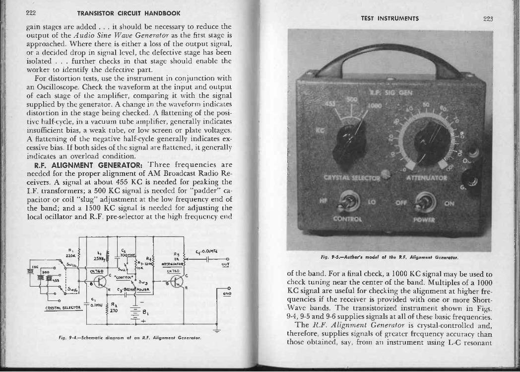
222 TRANSISTOR CIRCUIT HANDBOOKTEST INSTRUMENTS 223
gain stages are added . . . it should be necessary to reduce theoutput of the Audio Sine Wave Generator as the first stage isapproached. Where there is either a loss of the output signal,or a decided drop in signal level, the defective stage has beenisolated . . . further checks in that stage should enable theworker to identify the defective part.
For distortion tests, use the instrument in conjunction withan Oscilloscope. Check the waveform at the input and outputof each stage of the amplifier, comparing it with the signalsupplied by the generator. A change in the waveform indicatesdistortion in the stage being checked. A flattening of the posi-tive half -cycle, in a vacuum tube amplifier, generally indicatesinsufficient bias, a weak tube, or low screen or plate voltages.A flattening of the negative half -cycle generally indicates ex-cessive bias. If both sides of the signal are flattened, it generallyindicates an overload condition.
R.F. ALIGNMENT GENERATOR: Three frequencies areneeded for the proper alignment of AM Broadcast Radio Re-ceivers. A signal at about 455 KC is needed for peaking theI.F. transformers; a 500 KC signal is needed for "padder" ca-pacitor or coil "slug" adjustment at the low frequency end ofthe band; and a 1500 KC signal is needed for adjusting thelocal ocillator and R.F. pre -selector at the high frequency end
Fig. 9-4.-Schematic diagram of an R.F. Alignment Generator.
C AL T UATOR
Fig. 9-5.-Author's model of the R.F. Alignment Generator.
of the band. For a final check, a 1000 KC signal may be used tocheck tuning near the center of the band. Multiples of a 1000KC signal are useful for checking the alignment at higher fre-quencies if the receiver is provided with one or more Short -Wave bands. The transistorized instrument shown in Figs.9-4, 9-5 and 9-6 supplies signals at all of these basic frequencies.
The R.F. Alignment Generator is crystal -controlled and,therefore, supplies signals of greater frequency accuracy thanthose obtained, say, from an instrument using L -C resonant

224 TRANSISTOR CIRCUIT HANDBOOK TEST INSTRUMENTS 225
Fig. 9-6.-Interior view of the R.F. Alignment Generator-note crystal mounting.
circuits to determine operating frequencies. It is completelyself-contained, operating from a built-in battery power supply.Hence, there are no problems of "warm-up" time or shortterm frequency drift to limit its application. Further, the in-strument supplies an output signal of sufficient amplitude toalign even a weak receiver, with strong harmonics available tothe upper frequency limit of most Communications Receivers.
CIRCUIT DESCRIPTION: The instrument uses two R.F. typePNP transistors; one serves as a crystal -controlled oscillatorand is connected in a modified common -emitter configuration;the second transistor serves as a "buffer" or output amplifierand uses a standard common -emitter circuit arrangement.Power is supplied by a single 6 volt battery (B1), controlled by
a SPST toggle switch (SW,). Output impedance is approxi-mately 1000 ohms at full output.
In operation, R.F. Choke coil L1, shunted by loading ca-pacitor C2, forms the collector load for the oscillator stage.The feedback necessary to start and sustain oscillation is sup-plied through one of three quartz crystals, selected by switchSwi. The feedback is between collector and base circuits, withbase current established by resistor R1. The crystal selected bySw, determines the frequency of operation.
R.F. output is obtained from the oscillator across unby-passed emitter resistor R,, and is coupled through C3 to thebase of the buffer amplifier. Extracting an R.F. signal fromthe oscillator in this fashion minimizes circuit loading andassures maximum frequency stability. Base bias current forthe output stage is supplied through R4.
Carbon potentiometer R5 serves as the collector load for theoutput stage, with the amplified R.F. signal appearing acrossit coupled through D.C. blocking capacitor C4 to the OUT-PUT binding post. The setting of this control determines theoutput signal level.
Two other circuit components are of interest. Resistor R3,shunted by switch Sw2, can be used to reduce the D.C. appliedto the oscillator and amplifier circuits and thus to acts as a"Coarse" control on output level. Capacitor Cl serves as ageneral by-pass across the power supply.
PARTS LIST:
R1, R4 - 220K, 1/2 W. Carbon resistors.R, - 270 ohm, V2 W. Carbon resistor.R3 - 10K, 1/2 W. Carbon resistor.R3 - 1K Carbon potentiometer, Linear Taper (Centralab).Cl - 0.1 Mfd., 200 volt paper capacitor.C2 - 330 Mmf. tubular ceramic capacitor
(Centralab No. D6-331).C3 - 800 Mmf. disc ceramic capacitor
(Centralab No. DD -801).Cs - 0.01 Mfd., 600 volt tubular paper capacitor.

226 TRANSISTOR CIRCUIT HANDBOOK TEST INSTRUMENTS 227
L, - 2.5 MHy R.F. Choke (Superex No. F-25).Swiap Swib -2 Pole, 3 Pos. Rotary switch
(Centralab No. PA -1005).Sw,, Sw3 - SPST toggle switches.Bl -6 volt battery (Burgess No. Z4).Crystals - Quartz crystal, 455 KC, 500 KC, 1000 KC (HuppElectronic Corp. Type 20).Transistors - (2) Raytheon type CK760/2N112.MISC. - (2) transistor sockets; (2) control knobs; (2) bind-
ing posts; (3) Crystal sockets; small plastic handle; alumi-num case (/CA No. 29440); Tekni-Label decals; (4) rub-ber feet; machine screws, hex nuts, terminal strips, wire,solder, Misc. Hdwe.
CONSTRUCTION HINTS: Typical construction is clearlyshown in the exterior and interior views of the author's model,given in Figs. 9-5 and 9-6, respectively. Although the entireinstrument is assembled in an aluminum box measuring only3" x 4" x 5", there is no crowding of parts, nor any need touse subminiature components. An external "factory -built"appearance is obtained by using decals to label all controls.These are applied after all machine work (drilling, etc.) is
finished, but before parts are mounted, and are protected,after application, with two coats of clear plastic spray.
Although the transistor sockets are mounted on small sub -chassis, bent from scrap pieces of sheet metal, the crystalsockets are soldered directly to lugs on the CRYSTAL SELEC-TOR switch (Swi). The battery (B1) is held in place by a sim-ple "Z" bracket fastened to the side of the case with a singlemachine screw and nut.
After the wiring is completed, re -check all connectionsbefore installing the transistors. Make sure there are no wiringerrors, nor accidental shorts between bare leads. Pay especialattention to the battery connections . . . remember that polar-ity is important.
OPERATION AND USE: The transistorized R.F. AlignmentGenerator is somewhat easier to use than a conventional R.F.Signal Generator for two reasons . . . first, with no "warm-up"
time required, the instrument can be turned "ON" and"OFF" as often as is needed; secondly, frequency is selectedsimply by turning the CRYSTAL SELECTOR switch insteadof by setting a hard -to -read dial. The ATTENUATOR (R5),is used as a fine or "vernier" control on the output level, whilethe CONTROL switch (Sw2) is used as a "coarse" control.Maximum output is obtained when R3 is shorted out by Sw,. . . a peak signal of about 6 volts is available, or considerablymore than is furnished by the usual service instrument. Thisreserve is valuable for checking sets that are far out of align-ment.
The instrument furnishes an unmodulated (CW) signal.This means that a receiver's AVC voltage should be used as anindication of output rather than an audio signal level. Whenchecking the calibration of a Short -Wave or CommunicationsReceiver, the set's B.F.O. must be "ON".
To use in alignment, connect a shielded lead from theOUTPUT terminals to the receiver. Use a "dummy" antennaof the type recommended by the receiver manufacturer. Con-nect a VTVM or high resistance D.C. voltmeter across the re-ceiver's detector load resistor. Set the R.F. Alignment Gener-ator's CRYSTAL SELECTOR switch to 455 KC and turn upthe ATTENUATOR control until a reading is obtained onthe voltmeter; switch the CONTROL to "HI" output if nec-essary. Next, using an insulated alignment tool, adjust the I.F.transformers of the receiver for maximum output reading.Use the minimum signal necessary to obtain a good voltmeterreading to avoid overloading the receiver. Turn back theATTENUATOR control if necessary.
With the I.F. transformers peaked, switch to the 500 KCcrystal and set the receiver's dial to 1500 KC. Adjust the re-ceiver's local oscillator trimmer capacitor (usually located onthe tuning capacitor section with the smaller plates) for a peakvoltmeter reading. Adjust the pre -selector trimmer capacitorfor a peak reading. Next, tune the receiver to the 500 KCposition and, "rocking" the dial, adjust the "padder" capacitor

228 TRANSISTOR CIRCUIT HANDBOOKTEST INSTRUMENTS 229
(or oscillator coil's "slug") for a peak output. Recheck the1500 KC adjustment.
To use the instrument for checking the calibration of aCommunications Receiver, set the CRYSTAL SELECTORswitch to the 1000 KC crystal. Turn "ON" the receiver'sB.F.O. With the R.F. Alignment Generator set to near maxi-mum output, you should pick up "beats" at 1 megacycle(1 MC) intervals up to as high as your receiver will tune . . .
generally from 30 to 50 MC. If the receiver is properly cali-brated and aligned these beat signals should be obtained atexact dial settings . . . that is, 1 MC, 2 MC, 3 MC, 4 MC, 5 MC,6 MC, etc.
THE SIGNAL SQUIRTER: By far the majority of electronictest instruments are designed primarily for general purposeapplications, even though special models may be manufac-tured for the radio -electronic repair and servicing trades. Notso the instrument shown in Figs. 9-7 and 9-8 and shown in usein Fig. 9-9. This instrument, named The Signal Squirter bythe author, has been designed specifically for use as a servicingtool. It is intended to simplify the application of the "SignalInjection" diagnostic method in servicing amplifiers, broad-cast receivers, TV sets, and similar equipment.
The "Signal Injection" test method is generally applied to"dead" or "weak" receivers or amplifiers. Normally, an audioor R.F. test signal is obtained from a conventional Signal Gen -
CI )00e)(1,2N35 2N34
R,47K
43K
-=-.B, IOK- OUTPUT
LEVEL
I
3.1
It OUTPUT-0.02Ptio
Fig. 9.7.-Circuit for The Signal Squirter.
Fig. 9-8.-Interior view of The Signal Squirter.
erator and applied to various stages in the defective equip-ment, starting at the "output" stage and working back towardsthe first or "input" stage. The type of signal used, whetherA.F. or R.F., as well as its frequency, is changed in accordancewith the equipment being tested and the stage checked. Whenservicing a typical radio receiver, the technician would find itnecessary to change his signal several times . . . for an audiosignal is used for checking the audio stages, a modulated R.F.

230 TRANSISTOR CIRCUIT HANDBOOK TEST INSTRUMENTS 231
Fig. 9-9.-Using The Signal Squirter to service a transistorized receiver.
signal at the I.F. value for checking the I.F. amplifiers and de-tector, and, finally, a modulated R.F. signal at a broadcast fre-
quency for checking the R.F. and converter stages. Simplychanging frequencies and leads can require as much time asthe tests themselves.
The Signal Squirter permits the "Signal Injection" testmethod to be applied without changing test leads, withoutchanging frequencies, and without changing instruments. Itsupplies a complex signal which is basically an A.F. signal, butwhich contains rich harmonics through the AM BroadcastBand. In practice, it may be used to inject a signal at any pointin a typical AM receiver or audio stage. Its probe is simplytouched to the input of the stage to be checked. From its appli-cation, it is easy to see how the author derived the instrument'sname.
This instrument, working from its own self-contained bat-tery, requires no line cord, meter, or auxiliary equipment forits operation. And it works equally well with both vacuum -tube operated and transistorized equipment. What's more, theinstrument is so small that it can be slipped easily into a toolbox . . . or even into the serviceman's shirt pocket . . . makingit a truly portable instrument!
CIRCUIT DESCRIPTION: Referring to Fig. 9-7, we see thatThe Signal Squirter is basically a two -stage direct -coupledcomplementary amplifier, with capacity coupling between the"input" and "output" to convert the amplifier into an audiofrequency multivibrator. The common -emitter circuit con-figuration is used in both stages. Power is supplied by a single15 volt Hearing Aid battery (BO, controlled by a SPST switch(Sw1)
In operation, a type 2N35 NPN transistor is direct -coupledto a type 2N34 PNP unit through resistor R2. This resistorserves simply to limit D.C. current flow between stages andthus to protect the transistors. It is not essential to circuitoperation. Resistor R1 serves as the base resistor for the firststage; because of the direct -coupling, no base resistor is neededfor the second stage.
A potentiometer is used as the collector load for the secondstage and also serves as the OUTPUT control (R3). The "out-put" of the second stage is coupled back to the base of the first
stage through capacitor C1, changing the amplifier into amultivibrator.
The output signal, appearing across R3, and coupledthrough C2 to OUTPUT jack J1, is a sharp pulse, recurring atan audio rate. The pulse type of waveform is a complex signaland contains higher frequency harmonics of considerable am-plitude. In this case, the harmonics extend into, and through,the AM Broadctst Band (above 1600 KC), even though thebasic pulse repetition rate is at an audio frequency. Thus, ineffect, the circuit supplies both Audio and Modulated R.F.signals over a wide frequency range simultaneously.

232 TRANSISTOR CIRCUIT HANDBOOK
PARTS LIST:Ri - 47K, 1/2 W. Carbon resistor.R2 -4.7K, V2 W. Carbon resistor.R3 - 10K, subminiature potentiometer
(Centralab No. B16-2-).C1 - 800 Mmf., disc ceramic (Centralab DD-801).C2 - 0.02 Mfd., disc ceramic (Centralab DD -203).Sw1 - SPST switch, on R3.B1 - 15 volt Hearing Aid Battery (Burgess No. U10).J1 - Subminiature open circuit jack (Telex No. 9240).Transistors-(1) Sylvania type 2N35; (1) Sylvania type 2N34.MISC. - (2) transistor sockets; Subminiature plug (Telex
No. 9231); Small metal case; Ground lugs, machinescrews, nuts, wire, solder, Misc. Hdwe., etc.
CONSTRUCTION HINTS: The circuit is simple and non-critical and, therefore, subject to straightforward construction.No special precautions need be observed regarding either lay-out or lead dress. Of course, the builder should follow theusual "rules" of good wiring practice as far as transistor cir-cuitry is concerned . . . battery polarity should be observed,care should be taken not to overheat the transistor leads, andthe wiring should be double-checked for errors before thetransistors are installed.
Mechanically, the Signal Squirter may be housed in either aplastic or a metal case, but, from an electrical viewpoint, themetal housing is preferred because of its shielding character-istics. The author's model, shown in the photographs, washoused in a flat metal case. Some builders may prefer to use acylindrical housing, however, to give the completed instru-ment a conventional "Probe" appearance.
The output lead is a short length of fairly heavy bus bar,attached to the "hot" (center) terminal of a plug fitting jackJ1. In use, the instrument is held in one hand and this leadused as a test probe. For some work, a ground lead may be de-sirable . . . for such applications, a short length of flexiblehook-up wire attached to the metal case, and with a clip at thefar end, should be satisfactory.
TEST INSTRUMENTS 233
OPERATION AND USE: The average technician should re-quire relatively little practice to become skillful in using TheSignal Squirter. Typical usage is illustrated in Fig. 9-9. Theinstrument may be held in either hand, with one finger usedto manipulate the OUTPUT control and "ON -OFF" switch.The test probe is simply touched to the point at which thesignal is to be "injected" into the equipment under test. Insome cases, depending on the type of equipment being serv-iced and the defect encountered, a "ground" lead connectedbetween the instrument's case and the chassis of the equip-ment being tested will increase the signal level. This shouldbe needed only in rare cases, however.
When servicing a piece of "dead" or "very weak" equip-ment, the Signal Squirter is used is inject a signal into eachstage, starting at the output stage and working back towardsthe input. The output level should increase as each stage addsits gain. Where the output signal first drops appreciably, ordisappears entirely, the defective stage has been located! Fur-ther tests in that stage, using a conventional VoltOhmmeter,should isolate the defective part or parts.
The OUTPUT control is used to set the desired signallevel. In most work, the control is first set for maximum out-put, then gradually turned back as the signal is injected intoearlier stages. Care must be taken not to overload any onestage for this, in itself, may cause improper operation of theequipment and lead to false conclusions.
SQUARE -WAVE GENERATOR: A symmetrical rectangularwaveform, or "square -wave", is made up of a fundamental sinewave signal, plus odd harmonics of gradually decreasing am-plitude. Since the signal's waveshape depends on higher fre-quency harmonic content, as well as their relative amplitude,any loss or deterioration of higher frequency signals, or anyincrease in their amplitude, will result in a change from thenormal square -wave signal. Because of this characteristic, oneof the quickest ways to determine the approximate frequencyresponse of a non -tuned amplifier is to apply square -wave sig-nals at selected frequencies and to noteany changes in waveform.

234 TRANSISTOR CIRCUIT HANDBOOK
A "flat" amplifier will pass square -wave signals withoutchanging the waveshape. An amplifier with limited high fre-quency response, poor low frequency response, or a peak in itscharacteristics, will distort the square -wave signal. The typeof distortion varies with the frequency response of the ampli-fier. A skilled technician, by observing both the "input" and"output" square -wave signals of an Oscilloscope, can drawvalid conclusions about the characteristics of the amplifierunder test.
The circuit of a transistorized Square -Wave Generator, sup-plying signals at four different frequencies, and designed pri-marily for testing audio and instrument amplifiers, is given inFig. 9-10. The instrument is shown connected to a HeathkitOscilloscope in Fig. 9-11, while an interior view is given inFig. 9-12.
CIRCUIT DESCRIPTION: Three transistors are used in theinstrument . . . one PNP and two NPN units. A type 2N34PNP transistor and a type 2N35 NPN unit are connected toform a direct -coupled complementary multivibrator. A second
100K
SOC - 0.02 MEd
locoI
ca- CLOIMFol
C3- 0.000LMILSlug
110- .
FREQUENCY
2N34
II
E4 0.001Miel
2N35
R a
VOC
2N35CC- LOM61 c
a,SK r 22K,
Cs -%MU
g
Si 12 R
R53K
AMPLITUDE
C7 - 0.5M FJ
II -0 ovT
POWER
Fig. 9-10.-Schematic of a simple 4 -frequency Square -Wave Generator.
GND
TEST INSTRUMENTS
Fig. 9-11.-The Square -Wave Generator connected to an Oscilloscope.
235
type 2N35 is used as an output amplifier -clipper. OperatingPower is supplied by a single 15 volt Hearing Aid battery (B,),controlled by SPST toggle switch Sw2.
Refer to Fig. 9-10. A 2N34 and 2N35 transistor are direct -coupled in a complementary multivibrator very similar to thatused in the Signal Squirter described in an earlier project. Butthere are several important differences. First, a selector switch,Sw1, is used to choose any one of several feedback capacitors(C1, C2, C3, C4), thus providing a simple control on operating

236 TRANSISTOR CIRCUIT HANDBOOK TEST INSTRUMENTS 237
Fig. 9-12.-Interior view of the transistorized Square -Wave Generator.
frequency. Secondly, an unby-passed emitter resistor, R2, hasbeen added to the second stage; this resistor changes the out-put from a narrow pulse to a symmetrical rectangular wave.The use of R2, in the emitter circuit of the second stage, elimi-nates the need for an interstage current limiting resistor, sothe collector of the first stage is connected directly to the baseof the second stage. R, serves as the base resistor for the first(2N34) stage, while R3 serves as the output load.
The signal appearing across R3 is coupled through capacitorC, to the base input of the output stage, a common -emitteramplifier operated without bias current in order to obtain"clipping" action, further "squaring" the signal waveform.R4 serves as the base resistor for this stage, with potentiometerR5 serving the dual function of collector load and AMPLI-TUDE control. The final output signal is coupled through Cito the OUTPUT terminal.
PARTS LIST:R, - 100K, 1/2 W. Carbon resistor.R2 - 4.7K, 1/2 W. Carbon resistor . . . see text.R3 - 6.8K, 1/2 W. Carbon resistor . . . see text.R, - 22K, 1/2 W. Carbon resistor.R, - 3K Carbon potentiometer, Linear Taper
(Centralab No. B-8).C,* - 0.02 Mfd., 200 volt tubular paper capacitor.Co* - 0.01 Mfd., disc ceramic capacitor
(Centralab DD -1032).C,* - 0.002 Mfd., 200 volt tubular paper capacitor . . . or
disc ceramic.C4* - 0.001 Mfd., disc ceramic capacitor
(Centralab DD -102).*Frequency determining capacitors . . . see text.
C5 - 16 Mfd., 40 volt electrolytic capacitor(Barco No. P40-16).
Ca - 1.0 Mfd., 200 volt tubular paper capacitor.C7 - 0.5 Mfd., 400 volt tubular paper capacitor.Sw1 - One Pole, 4 Position rotary switch.Sw2 - SPST Toggle switch.B, - 15 volt Hearing Aid battery (Burgess No. Y10).Transistors-(1) Sylvania type 2N34; (2) Sylvania type 2N35.MISC. - (3) transistor sockets; (2) control knobs; (2) bind-
ing posts; Battery box (Austin -Craft No. 136); metal case(ICA No. 29441); (4) rubber feet; terminal strips, ma-chine screws, hex nuts, ground lugs, wire, solder, Misc.Hdwe., etc.
CONSTRUCTION HINTS: The construction details of theauthor's model are clearly evident in the exterior and interiorviews of his instrument, given in Figs. 9-11 and 9-12 respec-tively. The entire circuit, including battery, is easily assem-bled into the 3" x 51/4" x 2" aluminum box specified in thePARTS LIST; there is no crowding of parts. A small alumi-num sub -chassis, bent from scrap metal, supports the threetransistor sockets. For a final professional "touch", the com-pleted instrument was labeled with white decals.

238 TRANSISTOR CIRCUIT HANDBOOKTEST INSTRUMENTS 239
Since neither lay -out nor lead dress are critical, a prospec-tive builder may either follow the author's model or make upa new arrangement to suit his specific requirements. Careshould be taken to keep signal leads short and direct to mini-mize circuit distributed capacities, however. And, of course,special attention should be paid to battery and electrolyticcapacitor polarities.
Although circuit lay -out is not critical, the electrical valuesmay need some adjustment for optimum performance. Theseadjustments can be made best after wiring is completed anddouble-checked and after the instrument has been given a pre-liminary test by checking its output with an Oscilloscope.Specifically, adjustment must be made for output frequency,symmetrical waveform, and best quality waveshape.
The output frequency is changed by changing the values ofcapacitors C1, C2, C3 and C4. The frequencies of 50, 100, 500,and 1,000 (1 KC) C.P.S. used in the author's model werechosen arbitrarily for audio applications. To obtain exactfrequencies at any specific value, it may be necessary to useselected capacitors, due to normal parts tolerances. As an alter-native, each capacitor may be shunted with smaller units to"trim" to exact frequency.
A complementary multivibrator of the type used in this in-strument normally delivers a narrow output pulse. To obtaina symmetrical output waveform or true "square" wave, emit-ter resistor R2 has been added to the circuit. The ratio of R,and R3 will determine the symmetrical qualities of the outputwaveform . . . that is, whether the positive and negative half -cycles of the signal are of equal time duration. Adjust thesetwo resistors experimentally . . . a Resistance Substitution Boxis handy for this job . . . until the desired waveform is ob-tained. Remember that all values listed in Fig. 9-10 and thePARTS LIST are nominal only . . . final values are deter-mined experimentally to match the individual transistors used.
The final check is for the quality of the output waveform.The signal should have straight sides and a flat top. If the sig-nal is distorted, it may be that adequate clipping is not ob-
tained in the output stage. Try interchanging the two 2N35transistors . . . some of these work better as clippers thanothers. Also try varying the bias on this stage. Although nor-mally operated without bias, a small bias current may beadded by conecting a resistor from the base terminal to circuitground . . . this may have a value ranging from as low as 12Kto as high as 220K. Determine the best value experimentally.
OPERATION AND USE: The transistorized Square -WaveGenerator has three controls and two output terminals. Theinstrument is turned "OFF" and "ON" by the POWERswitch (Sw2); no warm-up time is required. The square -waverepetition rate or frequency is set to specific values by theFREQUENCY switch (Sw1). The output level is adjusted bythe AMPLITUDE control (R5); normally, the minimum sig-nal level needed to obtain observable results is used, to avoidpossible overload of the equipment under test. An Oscillo-
scope is a required accessory.To check the response of an amplifier, connect the OUT-
PUT terminals of the Square -Wave Generator to the INPUTof the unit. Use short, direct leads to minimize distributedcapacities. An Oscilloscope is used to check both the output ofthe generator and the output of the amplifier and the wave-forms are compared. Poor low frequency response and phaseshift is indicated by a "tilt" of the top of a 50 cycle signal. Poorhigh frequency response is indicated by a "rounding" of theforward square edge of a 1 KC signal. A peak in amplifier re-sponse may cause either a small "pip" or upward swelling onthe top of the square wave (which should be flat) or, in ex-treme cases, may cause a small "wiggle" in the output signal,due to transient oscillation brought about by shock excitation.
For a fairly thorough test, use all four output frequencies,noting the response of the amplifier to each. Try varying theAMPLITUDE control to make sure there is no overload inthe amplifier . . . output waveform should remain the same,except for height, regardless of the AMPLITUDE control'ssetting, up to the point where overload occurs.

240 TRANSISTOR CIRCUIT HANDBOOK TEST INSTRUMENTS 241
Generally speaking, it is possible, with practice, to deter-mine an amplifier's approximate response characteristics toabout the 10th or 20th harmonic of the square -wave signalused. Thus, a 1KC square -wave serves as a check to about10,000 or 20,000 C.P.S., depending on the skill of the operator.
PULSE GENERATOR: While all of the test instruments de-scribed thus far in this Chapter have had important applica-tions as radio -electronic servicing and repair aids, even if notdesigned expressly for such work, the instrument shown inFigs. 9-13 and 9-14 finds little, if any, application in the main-
aN
smc,.PULSE RUE
Fig. 9-I3.-Circuit of a transisorized Pulse Generator delivering both positive -goingand negative -going pulses.
tenance field. Its primary use is in the experimental labora-tory. The Pulse Generator supplies a repetitive signal of rela-tively short time duration, of variable output amplitude, andwith either a positive -going or negative -going characteristic.
Since the Pulse Generator serves as a source of a special typeof signal waveform, its applications vary considerably with theneeds and interests of the individual user. Typical applica-tions include . . . checking of delay lines and special circuitnetworks, use as a timing marker, triggering sweep circuits,transient response tests of wide -band amplifiers, shock -excita-tion of "ringing" circuits, and tests of electronic counter cir-cuits.
Fig. 9-14.-Exterior view of the Pulse Generator.
CIRCUIT DESCRIPTION: As we can see by reference to theschematic diagram given in Fig. 9-13, the transistorized PulseGenerator uses two PNP transistors. One is connected as ablocking oscillator, using a common -emitter circuit configura-tion; the other serves as an output amplifier, and uses a split -load circuit arrangement to obtain signals with opposite polar-ity characteristics. Operating power is supplied by a single 6volt battery, B1, controlled by a SPST switch (Sw1) and by-passed by a capacitor (CO to minimize interstage coupling aswell as to absorb switching transients.
In operation, transformer T, serves a dual purpose. Its cen-ter -tapped primary winding supplies the feedback necessary tostart and sustain oscillation in the first stage, while its second-ary winding serves to couple the oscillator's signal to theoutput amplifier stage. While the signal's waveshape is deter-

242 TRANSISTOR CIRCUIT HANDBOOK TEST INSTRUMENTS 243
mined primarily by the characteristics of the oscillator trans-former (T,), the frequency or Pulse repetition Rate is deter-mined by the R -C time constant in the base circuit of theoscillator . . . . that is, by coupling capacitor C, and base re-sistors R, and R2. By making R2 variable, we can provide asmooth control over PULSE RATE. The upper frequencylimit is determined by R, and C the lower limit by the totalvalue of R, and R2, plus C1.
The pulse signal obtained from the blocking oscillator stageis coupled through D.C. blocking capacitor C2 to the outputamplifier. This stage serves to provide signals of both positiveand negative polarity, and to act as a "buffer" to isolate theoscillator from the output, but provides little or no signalgain. Positive -going signal pulses are developed across collec-tor load R3; negative -going pulses across emitter load R4. ASPDT switch, Sw,, determines which signal is coupled throughcapacitor C4 to the OUTPUT CONTROL, potentiometer R5.
PARTS LIST:R1 - 47K, 1/2 W. Carbon resistor.R2 -5 Megohm Carbon potentiometer, Linear Taper
(Centralab B-87).R3, R4 - 2.7K, 1/2 W. Carbon resistors (see text).R, - 10K Carbon potentiometer, Linear Taper
(Centralab B-14).C C2 - 0.01 Mfd., disc ceramic capacitors
(Centralab DD6-1032).- 160 Mfd., 6 volt electrolytic (Barco No. P6-160).
C4 - 25 Mfd., 25 volt electrolytic (Barco No. P25-25).T1 - Transistor input transformer, 100K to 1500 ohms
(Argonne AR -102).Sw, - SPST Toggle switch.Sw2 SPDT Toggle switch.B, - 6 volt battery (Burgess No. Z4).Transistors - (2) RCA type 2N109.MISC. - (2) transistor sockets; (2) control knobs; (2) bind-
ing posts; aluminum case, 3" x 4" x 5" (L.M.B. No. 140);
(4) rubber feet; Machine screws, hex nuts, wire, solder,terminal strips, Misc. Hdwe., etc.
CONSTRUCTION HINTS: The author's model of the PulseGenerator was assembled in a standard aluminum box meas-uring 3" x 4" x 5", with plenty of room to "spare". A carefulbuilder should have no difficulty assembling the instrumentin an even smaller case . . . although any reduction in panelspace might crowd the controls. Signal leads should be keptshort and direct to minimize distributed capacities, but, other-wise, circuit lay -out and wiring are not critical. Of course, bat-tery and electrolytic capacitor polarities should be observed.
The "factory -built" appearance of the author's model, asshown in Fig. 9-14, is due almost entirely to the use of com-mercially available decals for labeling the instrument andcontrols, plus the use of an aluminum case pre -finished with agray hammerloid enamel.
There is only one point that might give the builder sometrouble . . . output resistors R3 and R4 may have to be ad-justed. In most cases, these two resistors can have the samevalue. However, where the builder wishes the positive -goingpulse and the negative -going pulse to have exactly the sameamplitude for a given setting of R5, then the final values ofthese two resistors may have to be determined experimentally.As an alternative, a 5K potentiometer may be substituted foreither R3 or R4. After construction and testing, this control isadjusted so that the two output pulses are of equal amplitude.
OPERATION: Typical positive -going output pulses, as sup-plied by the transistorized Pulse Generator, are shown in Fig.9-15. As can be seen, the pulses are reasonably narrow andhave a sharp leading edge. Except for polarity, the positive -going and negative -going pulses are virtually identical.
The instrument is equipped with four controls and twooutput binding posts, one of which serves as the GND termi-nal. The POWER switch and POLARITY control are simpletoggle switches. No warm-up time is required. The pulse fre-quency, or repetition rate, is set by the PULSE RATE con-trol; in the author's model, coverage was from 40 PPS to 400

244 TRANSISTOR CIRCUIT HANDBOOK TEST INSTRUMENTS 245
Fig. 9-M.-Positive-going pulses obtained from the instrument shown in Fig. 9-14.
PPS as R2 was adjusted. The output amplitude is set by theOUTPUT CONTROL (R,); maximum output of the au-thor's model was approximately 1.5 volts peak . . . an amplesignal level for low power and small signal testing. Currentdrain is very low, so battery life should equal the normal "shelflife" of the battery used . . . measured power consumption ofthe author's model was 50 microamperes at 6 volts.
SPECIAL INSTRUMENTSSINE WAVE CLIPPER: A clipped sine wave may be used as
a substitute for a square -wave signal for many basic tests. Thus,an electronics worker who does not feel that his need for aSquare -Wave Generator is great or pressing enough to justifyhis purchase or construction of such an instrument may prefer
IN
CK72Z
Fig. 9-16.-Schematic of a simple, but useful, test instrument-a Sine Wave Clipper.
to assemble a simple Sine Wave Clipper to use in conjunctionwith his standard A.F. Sine Wave Generator. The circuit forsuch an instrument is given in Fig. 9-16, while an assembledmodel is shown in Fig. 9-17 . . . the instrument is so small thatit can be held comfortably in the palm of the hand!
Fig. 9-17.-The Sine Wave Clipper fits easily into the palm of your hand.
CIRCUIT DESCRIPTION: The circuit used is extremely sim-ple, as can be seen by reference to the schematic diagram givenin Fig. 9-16. Basically, the Sine Wave Clipper is a single stageamplifier using a PNP transistor in the common -emitter con-figuration, and operated without base bias current. Power issupplied by a 15 volt Hearing Aid battery, B,, controlled bya SPST switch (Sw,) mounted on the OUTPUT control.
In operation, capacitors C, and C2 serve as input and outputD.C. blocking capacitors, respectively. R, serves as the baseresistor and OUTPUT control R, as the collector load resis-

246 TRANSISTOR CIRCUIT HANDBOOKTEST INSTRUMENTS 247
tor. When a transistor amplifier is operated without bias atfairly high signal levels, it becomes essentially a Class B ampli-fier, and converts applied signals into relatively narrow pulseswith rounded tops. Since some amplification occurs, the out-put signal level will be greater than the input signal.
If the amplifier has a resistive load (R2), the collector cur-rent can increase with increasing applied signal level only alimited amount . . . that is, to the point where the entire sup-ply voltage is dropped across the load resistor. At this point,the rounded tops of the output pulses are clipped off and theoutput signal becomes a rectangular pulse, with straight sidesand flat tops and bases . . . for practical purposes, an unsym-metrical square -wave; and it may be used as a square -wave forquick circuit tests!
Thus, when properly driven, the Sine Wave Clipper sup-plies pulse signals.
PARTS LIST:R, - 22K, V2 W. Carbon resistor.R2 - 10K Carbon potentiometer, Linear Taper
(Centralab B-14).C1, C2 - 1.0 Mfd., 200 volt metallized paper capacitors.Swi - SPST switch, on R2.B, - 15 volt Hearing Aid battery (Burgess Y10).Transistor - (1) Raytheon type CK722.MISC. - Transistor socket; control knob; (4) binding posts;
battery box (Austin -Craft No. 136); aluminum case(ICA No. 29435); Terminal strips, ground lugs, machinescrews, hex nuts, wire, solder, Misc. Hdwe., etc.
CONSTRUCTION HINTS: The average builder should havelittle or no difficulty assembling the Sine Wave Clipper intothe small case shown in the photograph and specified in thePARTS LIST if he takes time to plan component arrange-ment prior to starting assembly and wiring. Layout is non-critical, but all signal leads should be kept short and direct.The "factory -built" appearance of the model was obtained bylabeling the instrument with black decals. Available throughmost radio parts distributors, these decals are applied after
machine work is finished, but before parts are mounted andwiring started. The decals should be protected by at least twocoats of clear lacquer or Acrylic plastic for maximum life.
OPERATION: A standard A.F. Sine Wave Generator isconnected to the INPUT terminals and the OUTPUT ter-minals are connected to the equipment to be tested. Fairlyshort leads should be used to minimize high frequency signalloss due to distributed capacities. For proper drive and clip-ping, an input signal of between three and six volts is needed(from a standard 600 ohm source). The transistorized AudioSine Wave Generator described earlier in this Chapter cansupply sufficient drive only if an auxiliary amplifier is used.Good quality signals may be obtained over the range of from30 to 30,000 C.P.S., with proper drive. Maximum output isapproximately 15 volts peak -to -peak, but a lower signal levelis easily obtained by adjusting the OUTPUT control.
To use the Sine Wave Clipper for checking the response ofan amplifier, simply connect its OUTPUT to the input of theamplifier. Use an Oscilloscope to observe the waveshape of theclipped sine wave signal applied to the amplifier as well as theoutut signal obtained from amplifier. Note any deteriorationof signal waveform. A "rounding" of the sharp leading edgeof the pulse indicates poor high frequency response. A "tilt"in the flat base (or top) of in the signal indicates poor low fre-quency response or severe phase shift. Use a 50 to 100 C.P.S.signal for checking the low frequency response . . . a 5 to 10KC signal for checking high frequency response. Basic wave-form analysis is similar to that used in tests with a Square -Wave Generator (which see).
TRANSISTOR CHECKER: Experimenters and servicemenalike need some simple method for checking their transistors,at least until such time that their work can justify the purchaseof a laboratory type tester, such as the instrument shown anddescribed in Chapter 13. From a practical viewpoint, there arethree things a worker should know for a simple qualitative(Good or Bad?) evaluation of a transistor: Is the transistor"leaky" (or shorted)? Is the unit "open"? Does the transistor

248 TRANSISTOR CIRCUIT HANDBOOK TEST INSTRUMENTS 249
give reasonable gain? The circuit for a simple TransistorChecker which will answer these three questions is given inFig. 9-18, while exterior and interior views of an assembledmodel are given in Figs. 9-19 and 9-20, respectively. This in-
NPH
E
$w10
Sw3 Rt
TEST- GAIN 375K
Swa.ON- OPP
B'
SELECTOR
[IN *NW POSITION]Courtesy Lafayette Radio
Fig. 9-18.-Circuit for a simple Transistor Checker.
strument uses no expensive precision parts and requires nodifficult -to -make calibrations and, therefore, is an excellentproject for the student or home experimenter. It is suitablefor checking both PNP and NPN junction triode transistors.
CIRCUIT DESCRIPTION: Refer to the schematic diagramgiven in Fig. 9-18. The Transistor Checker makes a static(D.C.) test of the transistor's characteristics. Power is suppliedby a self-contained 15 volt Hearing Aid battery (B1), con-trolled by SPST toggle switch Sw1, while a D.C. Milliammeterserves as an indicating device.
In operation, the four -pole -two -position SELECTOR switchSly, acts to reverse the battery and meter polarities, to permittesting both PNP and NPN units. In the "TEST" position
C E
ON PNP NPN TEST
Fig. 9-19.-Author's model of the Transistor Checker.
(Sw3 open), a D.C. voltage is applied to the transistor's emitterand collector electrodes, with the meter in series to read re-sulting current flow; the transistor's base electrode is left"floating" (open) during this test. If the transistor is "Good",current flow should be low, with its value proportional to thetransistor's collector cut-off current (Ic0. A small up-scalemeter reading may be expected of some units, but if more than

250 TRANSISTOR CIRCUIT HANDBOOK TEST INSTRUMENTS 251
Fig. 9-20.-Interior view of the Transistor Checker.
a quarter -scale reading is obtained, it indicates that the tran-sistor is "leaky" (has high 'co). A greater than full-scale readingindicates that the transistor is probably shorted.
When switch Sw3 is thrown to the GAIN position (closed),a small base bias current is applied through resistor R per-mitting an increase in collector -emitter current flow. An up-scale meter reading should be obtained, with the reading pro-
portional to the transistor's gain (beta). If there is no currentflow indicated on the meter, the transistor is "open". A smallreading indicates low gain, a high reading good gain (assumingthe "leakage" current to be low).
PARTS LIST:
R1- 375K, 1 W. Carbon resistor, 5% tolerance (made up360K, 1/2 W. and 15K, V2 W. resistors in series).
SwiA, SwiB, Swic, Swii, - 4P-2Pos. Rotary switchSw2, Sw3 - SPST Toggle switches.B1 - 15 volt Hearing Aid battery (Burgess No. Y10).METER - 0-2 Milliamperes D.C. Milliammeter, high re-
sistance coil (Sterling No. 835, Type 68N).MISC. - Transistor socket; Battery box (Austin -Craft No.
136); control knob; metal case (L.M.B. No. 136); (4) rub-ber feet; Machine screws, nuts, wire, solder, Misc. Hdwe.,etc.
(NOTE: Lafayette Radio, 100 Sixth Ave., New York 13,N. Y. offers a "kit" for assembling an instrument of thistype.)CONSTRUCTION HINTS: The lay -out and construction of
the author's model is clear from the exterior and interior viewsgiven in Figs. 9-19 and 9-20. Black decals were used to labelthe instrument and controls. Since only D.C. circuits are in-volved, neither parts arrangement nor lead dress are critical,and since no semiconductors are used in the circuit proper, nospecial precautions against heat damage are needed. The in-dividual builder may either follow the author's lay -out ormake up a new one to suit his own inclinations. After assem-bly is completed, however, all wiring should be double-checkedfor accuracy, with special attention to battery and meterpolarities.
OPERATION AND USE: Testing a transistor with the Tran-sistor Checker is simplicity itself. First, determine the type oftransistor to be tested (NPN or PNP), referring to the tablegiven in Chapter 11 if necessary, and set the SELECTORswitch (Sw1) accordingly. With Sw3 in the TEST position, close

252 TRANSISTOR CIRCUIT HANDBOOK TEST INSTRUMENTS 253
the ON -OFF switch (Sw2) and insert the transistor in its socket.A "Good" transistor should cause little, if any, meter deflec-tion . . . the maximum reading should not exceed 0.5 milli-amperes (1/4 scale deflection). Readings in excess of this valueindicate that the transistor has a high cut-off current (I.) andmay be considered excessively "leaky" . . . if a greater thanfull scale reading is obtained, the transistor may be considered"shorted".
To check for gain, throw Sw3 to the GAIN position (closingit) and again note meter reading. An up-scale reading shouldbe obtained, with the reading proportional to transistor gain.If a "zero" meter reading was obtained in the first test, thenthe transistor's beta may be approximated by multiplying theactual meter reading by 25. Thus, if a reading of 1.2 milli-amperes is obtained, beta is approximately 30. If a greaterthan "zero" reading was obtained in the first test, this multi-plying factor does not hold. High gain transistors may give agreater than full-scale reading . . . this does not indicate a de-fective unit. On the other hand, if "zero" meter readings areobtained with both the leakage and gain tests, the transistor isopen.
In addition to its application in basic transistor tests, theTransistor Checker is also valuable for selecting transistorswith special characteristics. For example, it might be used toselect the highest gain transistor out of a group of similarunits. Or it might be used for obtaining a "matched pair" oftransistors for push-pull applications. Or it could be used forselecting a unit with low D.C. leakage for D.C. amplifierapplications.
Several modifications in the basic circuit may be made, ifdesired by the individual builder. First, since current is drawnonly when a transistor is inserted in the socket, ON-OFFswitch Sw2 may be left out of the circuit . . . simply connectthe battery direct to switch Swls. A second modification,which may appeal to some builders, is the substitution of apush-button switch for Sw3 in place of the Toggle switch speci-fied in the PARTS LIST and shown on the model.
TEST METERS
METER AMPLIFIERS: Some types of technical and scientificwork require the measurement of extremely small direct cur-rents-on the order of several microamperes, or less. Metersfor measuring such small currents, while available, are gener-ally very expensive and quite delicate, hardly suitable for thecomparatively rough usage encountered in a typical labora-tory. Fortunately, the sensitivity of a D.C. meter may be in-creased considerably by adding a direct-coupled transistoramplifier. The overall sensitivity of the combination dependsboth on the sensitivity of the basic meter movement and onthe gain (beta) of the transistor used. Gain multiplying factorsof 10 to 50 are fairly easy to achieve with commonly availabletransistors. For higher gains, two or more transistors may beused in cascade.
Two typical Meter Amplifier circuits are given in Fig. 9-21.The circuit shown in Fig. 9-21(a) uses a single transistor todrive a meter. The circuit given in Fig. 9-21(b) uses two tran-sistors in cascade to achieve higher gain; in addition, calibra-
PNP
(0.) (b)
Fig. 9-21.-Circuits for two transistorized Meter Amplifiers-(a) Single Stage and(6) Cascaded Stages.

254 TRANSISTOR CIRCUIT HANDBOOK TEST INSTRUMENTS 255
tion and zero adjustment provision has been added to the
latter circuit.CIRCUIT DESCRIPTION: With junction transistors, the com-
mon -emitter circuit is used almost universally for D.C. ampli-
fication, except where impedance matching considerations or
other factors dictate the use of the common -collector or com-
mon -base configurations. The circuit shown in Fig. 9-21(a)
represents the basic D.C. amplifier. In operation, the transistor
is operated without base bias current and meter current is
essentially the "leakage" current of the transistor. With a good
quality transistor, the "zero input" meter reading should ap-
proximate zero. When the amplifier is connected into a D.C.
circuit, current flowing through the circuit becomes, essen-tially, the base "bias" current of the transistor. A flow of bias
current allows collector current to flow, giving an up-scale
meter reading. Collector current is of much greater magnitudethan base current, of course, due to the gain of the transistor.
Thus, the gain of this circuit is directly proportional to the
beta of the transistor used.Greater gain is obtained when two transistors are connected
in cascade, as shown in Fig. 9-21(b). The common -emitter con-
figuration is used in both stages. Although operating essen-
tially like the basic circuit, several refinements have been
made to insure more linear operation. First, both stages are
biased . . . the bias current for the first stage is determined by
R1, in conjunction with the adjustment of R2. The bias cur-
rent of the second stage is determined by R4 and R5, plus the
"zero input" current of the first stage (and hence, to some ex-
tent, on the setting of R2). Finally, a bridge type output circuit
is employed . . . the "upper" arms of the bridge circuit arecollector load resistor R, and Potentiometer R2, the "lower"
arms of the bridge are potentiometer R3 and the emitter -
collector circuit of the second stage; the meter (M) is con-
nected directly across the bridge. Since bias adjustment con-
trol R2 is part of the output circuit, it contributes a certain
amount of feedback to the input, helping to stabilize the cir-
cuit with variations in transistor characteristics.
PARTS LIST-Fig. 9-21(a):B, - 1.5 volt to 6 volt battery.M - Meter . . . 100 microamperes to 2 milliamperes
(see text).Transistors - Any small signal PNP type . . . examples, GE
2N107, 2N45; Raytheon CK722, CK721; Sylvania 2N34;Transitron 2N34; Germanium Products 2N103, 2N98;etc.
MISC. - Small meter case; (2) binding posts; Machinescrews, nuts, wire, solder, Misc. Hdwe., etc.
PARTS LIST-Fig. 9-21(b):R, - 390K, 1/2 W. Carbon resistor.R2 - 1200 Ohm, Carbon or wirewound potentiometer.R3 - 250 Ohm, Carbon or wirewound potentiometer.R4 - 5.6K, 1/2 W. Carbon resistor.R,, R, - 560 Ohm, 1/2 W. Carbon resistors.Sw, - SPST Toggle switch.B, - 1.5 to 4.5 volt battery.M - Meter . . . 100 microamps. to 2 milliamps. (see text).Transistors - See text.MISC. - Small meter case; (2) binding posts or tip jacks;
(2) control knobs; Battery box; Machine screws, nuts,wire, solder, Misc. Hdwe., etc.
CONSTRUCTION HINTS: Construction of either of the twoMeter Amplifier circuits shown should be simple and straight-forward. With only D.C. circuits involved, both lay -out andlead dress are non -critical. There are a few points which thebuilder should keep in mind, however. First, since most cir-cuit currents are on a low order of magnitude, it is importantthat circuit resistances be kept low; for this reason, it is rec-ommended that the transistors be wired permanently into thecircuit, to avoid the resistances developed in the pressure con-tacts used in sockets. The usual precautions to avoid over-heating of transistor leads should be observed.
Almost any D.C. meter may be used in either circuit, de-pending on the overall sensitivity desired. Maximum sensi-
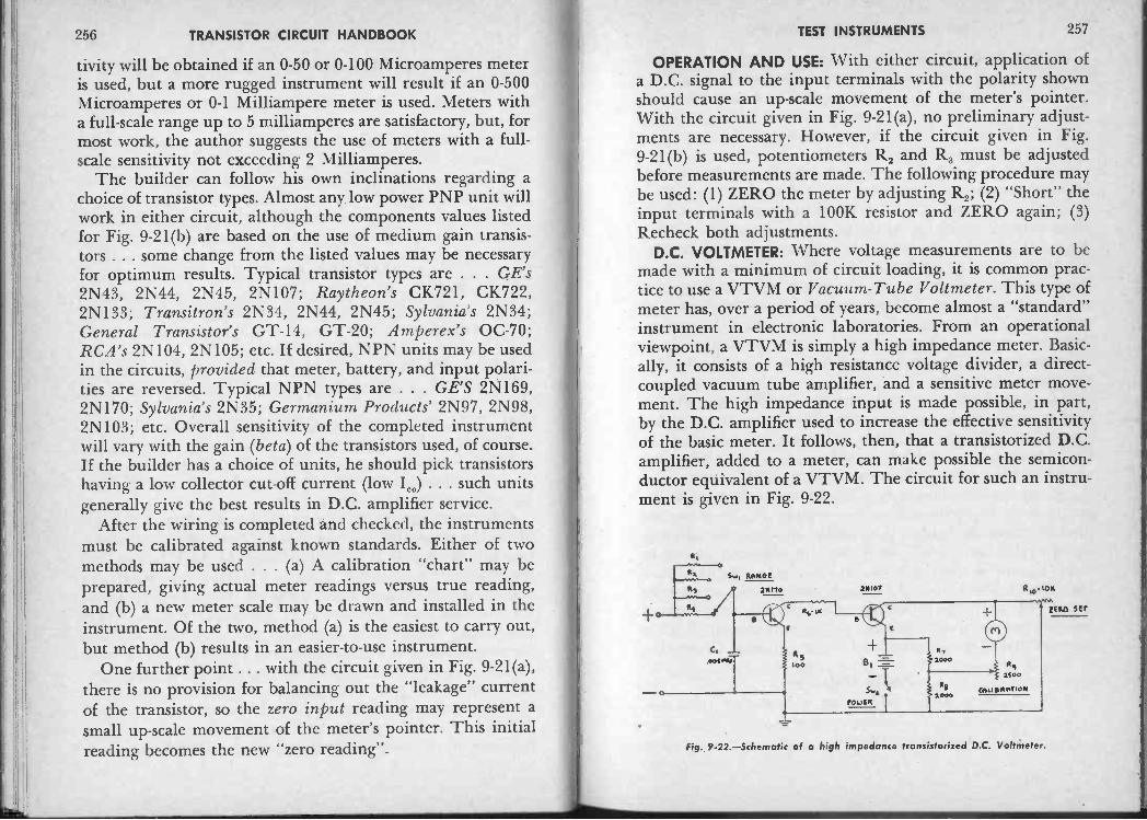
256 TRANSISTOR CIRCUIT HANDBOOK TEST INSTRUMENTS 257
tivity will be obtained if an 0-50 or 0-100 Microamperes meteris used, but a more rugged instrument will result if an 0-500Microamperes or 0-1 Milliampere meter is used. Meters witha full-scale range up to 5 milliamperes are satisfactory, but, formost work, the author suggests the use of meters with a full-scale sensitivity not exceeding 2 Milliamperes.
The builder can follow his own inclinations regarding achoice of transistor types. Almost any low power PNP unit willwork in either circuit, although the components values listedfor Fig. 9-21(b) are based on the use of medium gain transis-tors . . . some change from the listed values may be necessaryfor optimum results. Typical transistor types are . . . GE's2N43, 2N44, 2N45, 2N107; Raytheon's CK721, CK722,2N133; Transitron's 2N34, 2N44, 2N45; Sylvania's 2N34;General Transistor's GT-14, GT-20; Amperex's 0C-70;RCA's 2N104, 2N105; etc. If desired, NPN units may be usedin the circuits, provided that meter, battery, and input polari-ties are reversed. Typical NPN types are . . . GE'S 2N169,2N170; Sylvania's 2N35; Germanium Products' 2N97, 2N98,2N103; etc. Overall sensitivity of the completed instrumentwill vary with the gain (beta) of the transistors used, of course.If the builder has a choice of units, he should pick transistorshaving a low collector cut-off current (low Ico) . . . such unitsgenerally give the best results in D.C. amplifier service.
After the wiring is completed and checked, the instrumentsmust be calibrated against known standards. Either of twomethods may be used . . . (a) A calibration "chart" may beprepared, giving actual meter readings versus true reading,and (b) a new meter scale may be drawn and installed in theinstrument. Of the two, method (a) is the easiest to carry out,but method (b) results in an easier -to -use instrument.
One further point . . . with the circuit given in Fig. 9-21(a),there is no provision for balancing out the "leakage" currentof the transistor, so the zero input reading may represent asmall up -scale movement of the meter's pointer. This initialreading becomes the new "zero reading".
OPERATION AND USE: With either circuit, application ofa D.C. signal to the input terminals with the polarity shownshould cause an up -scale movement of the meter's pointer.With the circuit given in Fig. 9-21(a), no preliminary adjust-ments are necessary. However, if the circuit given in Fig.9-21(b) is used, potentiometers R2 and R3 must be adjustedbefore measurements are made. The following procedure maybe used: (1) ZERO the meter by adjusting R2; (2) "Short" theinput terminals with a 100K resistor and ZERO again; (3)Recheck both adjustments.
D.C. VOLTMETER: Where voltage measurements are to bemade with a minimum of circuit loading, it is common prac-tice to use a VTVM or Vacuum -Tube Voltmeter. This type ofmeter has, over a period of years, become almost a "standard"instrument in electronic laboratories. From an operationalviewpoint, a VTVM is simply a high impedance meter. Basic-ally, it consists of a high resistance voltage divider, a direct -
coupled vacuum tube amplifier, and a sensitive meter move-ment. The high impedance input is made possible, in part,by the D.C. amplifier used to increase the effective sensitivityof the basic meter. It follows, then, that a transistorized D.C.amplifier, added to a meter, can make possible the semicon-ductor equivalent of a VTVM. The circuit for such an instru-ment is given in Fig. 9-22.
Fig. 9-22.-Schematic of o high impedance transistorized D.C. Voltmeter.

258 TRANSISTOR CIRCUIT HANDBOOK TEST INSTRUMENTS 259
CIRCUIT DESCRIPTION: The transistorized high impedanceD.C. Voltmeter uses a two -stage amplifier, employing PNPand NPN transistors in a direct -coupled complementary am-plifier circuit. The common -emitter circuit configuration isused in both stages. Operating power is supplied by a single 6volt battery, controlled by SPST switch Sw2.
Referring to Fig. 9-22, resistors R1, R2, R3 and R4, selectedby selector switch Sw1, together with the moderate input im-pedance of the type 2N170 NPN transistor, form a simpleseries network which limits the maximum base current for agiven D.C. voltage applied to the input terminals. These re-sistors thus serve to determine the different voltage ranges ofthe instrument. Capacitor C1, from base to circuit ground,serves to by-pass any A.C. components in the applied D.C.voltage and, otherwise, is not essential to circuit operation.The unby-passed emitter resistor R5 serves the dual functionof helping to stabilize the first stage and of increasing its effec-tive input impedance.
D.C. amplification occurs in the first (NPN) stage, with itsoutput direct -coupled to the second (PNP) stage through cur-rent limiting resistor R6. After additional amplification, thefinal output is used to drive a simple bridge circuit consistingof the emitter -collector impedance of the 2N107 transistor,R7, R8, and potentiometer R10. The indicating meter (M), to-gether with its series calibrating resistor, R9, is connecteddirectly across the bridge. The bridge circuit is initially bal-anced under "no signal" conditions by adjusting one of itsarms (R10). This effectively cancels the effect of any D.C. pass-ing through 2N107 due to "leakage" and permits zeroing themeter. When a signal is received, the bridge is thrown out ofbalance and an up -scale meter reading is obtained, which isproportional to the amplitude of the amplified D.C. signal.
PARTS LIST:
R1, R2, R3, R4 - Range calibrating resistors (see text).R, - 100 ohm, V2 W. Carbon resistor.R6 - 1K, 1/2 W. Carbon resistor.
R7, R, - 2K, y2 W. Carbon resistors.R9 - 2500 ohm Carbon potentiometer, Linear Taper
(Centralab B-7).R10 - 10K Carbon potentiometer, Linear Taper
(Centralab B-14).C1 - 0.005 Mfd., disc ceramic (Centralab MD -502).Sw1 - Rotary selector switch, 1 pole (see text) . . .
(Centralab PA -2001).Sw2 - SPST Toggle switch.B1 -6 volt battery (Burgess No. Z4).M - Meter . . . 0-100 Microamperes to 1 Milliamperes
(see text).Transistors - (1) GE 2N170; (1) GE 2N107.MISC. - (2) Binding posts; (3) control knobs; Battery box
(Austin -Craft No. 110); metal case (ICA No. 29442); (4)rubber feet; small handle; terminal strips; Machinescrews, nuts, wire, solder, ground lugs, Misc. Hdwe., etc.
CONSTRUCTION HINTS: With neither parts lay -out norlead dress critical, this instrument is well suited to assemblyusing either "conventional" metal chassis construction or thenewer etched circuit techniques. An etched circuit boardmight very well be designed to mount on the back of the meteritself (M). For information on Printed Circuit Technique,refer to Chapter 13. Although transistor sockets may be in-stalled, the author feels it is best to wire these components inplace in an application of this type. Exercise care in protectingthese components against heat damage during installation.
Meters with a full scale sensitivity of from 100 microam-peres to 1 milliampere may be used in this circuit. The averagebuilder will probably prefer to use the popular 1 MA meter,but, of course, the more sensitive the meter movement, thegreater the overall sensitivity of the instrument. The numberof range resistors required (R1, R,, R3, R4, etc.), as well astheir individual values and the number of positions on therotary RANGE switch (Sw1), will depend on the number ofranges the builder wishes in his own instrument, on theirmaximum value, and on the basic meter movement used

260 TRANSISTOR CIRCUIT HANDBOOK
(and hence on overall sensitivity). If desired, a conventional"tapped" voltage divider resistor multiplier network may besubstituted for the individual resistors shown in Fig. 9-22. Formaximum accuracy in setting up the basic ranges, subminia-ture "trimmer" potentiometers may be used in place of fixedresistors for each range (R R2, R3, etc.). These may be ar-ranged in a "bank" in the final instrument . . . a typical ar-rangement of such units is illustrated in Fig. 9-23.
Fig. 9-23.-Range calibration potentiometers used in a transistorized meter circuit.
After the wiring is completed and checked, the instrumentmust be calibrated. Generally, the range resistors (R1, R2, R3,etc.) are chosen to give full-scale meter deflection when themaximum voltage of each range is applied to the "input" ter-minals. CALIBRATION rheostat R3 may be set to from 50to 500 ohms, depending on the resistance of the meter move-ment used; after the range resistors are chosen and installed,
TEST INSTRUMENTS 261
R3 is used as a vernier control for setting the full-scale reading. . . this is done by setting the instrument to its lowest rangeand, after adjusting R10 for a "zero" reading with no input,applying an accurate test voltage equal to full-scale reading ofthat range. The CALIBRATION control is then readjustedto give a full-scale reading.
Either of several methods may be used for making up thefinal scale calibrations. First, of course, known D.C. voltagesare applied and the actual meter readings noted, enabling theworker to prepare a "table" correlating actual meter readingswith applied voltages. If desired, the table may be used alone,with the operator interpolating in-between values. Or thesereadings may be plotted on a smooth curve, using regulargraph paper . . . the resulting curve is then used as a Calibra-tion Chart for the instrument. Finally, a new dial may bemade up for the instrument, giving actual voltage readingsinstead of current values.
OPERATION: The instrument is used in much the samemanner that any voltmeter is employed, except for the initial"setting" up. Turn the instrument "ON" by closing POWERswitch Sw2. No warm-up time is needed. Set the RANGEswitch to its lowest range. Adjust ZERO SET control R10 to"zero" the meter. Apply a known D.C. voltage to the inputterminals, observing polarity. This voltage should be equal tothe full-scale reading of the range to which Sw1 is set. AdjustCALIBRATION control R, for a fullscale reading. Finally,re -check the ZERO SET control. The instrument is now readyfor use.
In general, the ZERO SET and CALIBRATION controlsshould hold their settings reasonably well. Readjustmentshould be necessary only with aging of the battery and changesin the transistors' characteristics due to changing ambient
temperatures.Like any sensitive meter, care must be taken not to overload
the instrument. When making voltage measurements, startwith the highest range unless you are reasonably sure of theapproximate voltages in the circuit under test.

969 TRANSISTOR CIRCUIT HANDBOOK TEST INSTRUMENTS 263
LIGHT METERS: Architects, electrical engineers, educationaladvisors, office managers, illumination engineers, industrialpsychologists, efficiency specialists, interior designers and in-dustrial engineers are but a few of the groups who may useLight Meters in their work. Applications range from deter-mining the relative illumination levels in schools, offices,shops and factories, to the analysis of the reflectivity character-istics of paints, draperies, wall paper, or other wall and ceilingcoverings. Photographers, both amateur and professional, arelarge users of these instruments.
The simplest Light Meter is a self -generating photocell (or"sun battery") connected to a sensitive meter movement. Suchinstruments have limited sensitivity, due to the limited outputof the photocells; and, because of the sensitive meter move-ment used, are subject to shock and vibration damage. Semi-conductor photocells are used in most of these instruments,supplying essentially a D.C. output.
Since the transistor, itself a semiconductor device, makes anexcellent D.C. amplifier, a logical move would be a "marriage"of a photocell and a transistor amplifier into one instrument.
R7.
2N34
ALTE11110. COMMTION
R,2K
(a) (b)Fig. 9-24.-Two Light Meter circuits-(a) Basic circuit using a selenium photocell and
(b) Basic circuit using a Cadmium Sulfide photocell.
Such an arrangement will provide an instrument of greatersensitivity; in addition, ruggedness should be greater, since thegain of the transistor will permit the use of an indicatingmeter less delicate than the one required with a photocellalone.
Circuits for three different transistorized Light Meters aregiven in Figs. 9-24 and 9-25. Basic circuits, using a single tran-
2 N197 21197
as
Fig. 9-25.-A very Sensitive Light Meter circuit featuring a cascaded complementary amplifier.
1N1T
0010
2N107
lig27t
211107
ca INN
R!'so, so
C
a,
c.!.cc
c).[!!! Tin)
I +
sue,e
POWER
Fig. 9-26.-Schematic of an easily built Audio Level Meter.
... RFC Die Tort]
)
sistor, are given in Fig. 9-24, while a more sensitive circuit,using two transistors in cascade, is shown in Fig. 9-25. The twocircuits given in Fig. 9-24, while basically similar, illustratethe use of two different types of photocells.

264 TRANSISTOR CIRCUIT HANDBOOK TEST INSTRUMENTS 265
CIRCUIT DESCRIPTION: Referring to Fig. 9-24(a), a PNPtransistor serves as a one -stage direct -coupled amplifier. Thecommon -emitter configuration is used. Power is supplied by asingle battery, B1, controlled by SPST switch Sw1. In opera-tion, with no light falling on the photocell (PC,), base currentis virtually zero, and hence collector current, as indicated bymeter M, is at a minimum value. When light falls on the self -generating photocell, a small current is produced. This be-comes the base bias current for the transistor and permits aconsiderably larger collector current to flow, due to the gainof the transistor, and gives an up -scale reading on the meter.As more light falls on the photocell, base current, and thuscollector current, both increase. The meter (M) is shunted bya simple rheostat, R1, which serves as the Sensitivity control.As R1 is reduced in value, more of the collector current can beby-passed around the meter, reducing the meter reading for agiven light intensity.
An alternate connection for the positive lead of the photo-cell is shown dotted in the schematic diagram. Instead of re-turning to the positive terminal of the power supply, it is re-turned, through R2, to the negative side of the circuit. Thisprovides a small bias on the photocell and increases circuitsensitivity slightly. Optimum bias, for a given photocell andtransistor, is determined by making R2 adjustable.
The circuit shown in Fig. 9-24(b) uses a photoconductiverather than a "self -generating" type of photocell. With theformer, no current is developed by light falling on its sensitivesurface; instead, its resistance changes. To utilize this changeof resistance, the photocell is biased by a separate battery, B1,which, in turn, is controlled by switch Sw1. The bias currentis limited by series resistor R1 and CALIBRATION controlR2. This circuit, like the first one, also uses a single PNP tran-sistor as a common -emitter amplifier. Transistor operatingpower is supplied by a second battery, B2, controlled by switchSw2, which, in practice, is ganged with the "bias" switch Sw1.
In addition to using a different type of photocell, the circuitgiven in Fig. 9-24(b) differs from the first one in another im-
portant respect . . . the simple series meter circuit has beenreplaced by a bridge arrangement, to permit "balancing" outany steady collector current which may flow due to inherent"leakage" (high Ico) in the transistor. The upper arms of thebridge are made up by ZERO adjustment potentiometer R4.The lower arms of the bridge consists of the emitter -collectorcircuit of the transistor and resistor R3. The meter (M) isconnected across the bridge.
Greater sensitivity is obtained by cascading two NPN tran-sistors in a direct -coupled amplifier in the circuit given in Fig.9-25. A "self -generating" photocell (PC) is used with this cir-cuit so only one battery (B1) is needed for operation; it is con-trolled by POWER switch Sw1. Base bias for the first stageis furnished both by the photocell PC and through resistor R1,which has a relatively high value. Both stages use the common -emitter configuration. The first stage is direct -coupled to thesecond stage, with the base bias current for the second stagedetermined by the collector current of the first stage, as wellas by SENSITIVITY control R3 and fixed resistor R2.
The amplified output of the second stage is coupled to theindicating meter M through a bridge network, permitting the"dark" (no signal) current of the output transistor to be bal-anced out. The upper arms of the bridge are made up of fixedresistor R5 and part of ZERO ADJUST potentiometer R4.The lower arms of the bridge are made up of the emitter -collector impedance of the output transistor and the remain-ing part of potentiometer R4. The meter is connected directlyacross the bridge.
In operation, light falling on the photocell (PC) results inan increase in the base current of the first stage. This, in turn,causes a much larger change in the collector current, due tothe gain of the transistor. As the collector current of the firststage changes, the base bias current of the second stage changesin a similar manner, with its amplified output changing thebalance of the bridge circuit and permitting an up -scale read-ing on the meter.

266 TRANSISTOR CIRCUIT HANDBOOK TEST INSTRUMENTS 267
PARTS LIST-Fig. 9-24(a):R, - 2K, Carbon or wirewound potentiometer.R2 - 1 Megohm Carbon potentiometer (alternate circuit).PC, - "Self -generating" selenium photocell
(International Rectifier Co. type B2M).M - Meter . . . 0-100 microamperes to 0-1 milliamperes
(see text).SPST Toggle switch.
B, -3 volt battery (Two Burgess No. Z in series).Transistor - (1) Transitron type 2N34.MISC. - Transistor socket; aluminum or plastic case; con-
trol knob; battery box (Austin -Craft No. 124); terminalstrips; Machine screws, nuts, wire, solder, Misc. Hdwe.,etc.
PARTS LIST-Fig. 9-24(b):R, - 120K, 1/2 W. Carbon resistor.R2 - 100K Carbon potentiometer (Centralab B-40).R, - 2.2K, I/2 W. Carbon resistor.R, - 10K Carbon potentiometer (Centralab B-14).PC, - Cadmium Sulfide photocell (RCA No. 6694).M - Meter . . . 0-100 microamperes to 0-1 milliamperes
(see text).Sw Sw2 - DPST Toggle switch.
B, - 221/2 volt Hearing Aid battery (Burgess No. U15).B2 -6 volt battery (Burgess No. Z4).Transistor - (1) Transitron type 2N34.MISC. - (2) transistor sockets; aluminum or plastic case;
(2) control knobs; (2) battery boxes (Austin -Craft No.113 for 221/2 volt battery, No. 110 for 6 volt battery); lens(optional); terminal strips; Machine screws, nuts, wire,solder, Misc. Hdwe., etc.
PARTS LIST-Fig. 9-25:R, - 3.9 Megohm, 1/2 W. Carbon resistor.R2 - 10K, 1/2 W. Carbon resistor.R2 - 1 Megohm Carbon potentiometer (Centralab B-69).R4 - 25K Carbon potentiometer (Centralab B-26).
R. - 22K, y2 W. Carbon resistor.PC - "Self -generating selenium photocell
(International Rectifier Co. type B2M).M - Meter . . . 0-100 microamperes to 0-1 milliamperes
(see text).Swi-SPST Toggle switch.B, -6 volt battery (Burgess No. Z4).Transistors - (2) Germanium Products type 2N97.MISC. - (2) transistor sockets; aluminum or plastic case;
(2) control knobs; battery box (Austin -Craft No. 110);lens (optional); terminal strips; Machine screws, nuts,wire, solder, Misc. Hdwe., etc.
CONSTRUCTION HINTS: The same construction techniquesmay be applied to any of the three transistorized Light Metercircuits. Either "conventional" or Printed Circuit wiringmethods may be employed (see Chapter 13). Good wiringpractice should be followed, of course, but neither parts ar-rangement nor lead dress are critical.
Although PNP transistors are specified for the circuits givenin Fig. 9-24 and NPN units for the circuit given in Fig. 9-25,the opposite types may be used in either circuit, provided allD.C. polarities are reversed. The transistor used in the simplecircuit given in Fig. 9-24(a) should be selected for a low col-lector cutoff current (Ico) to avoid too high a "dark" readingon the meter. However, since the other two circuits employ abridge balancing arrangement in their output, this factor isnot as important.
The selenium photocells specified for the circuits given inFigs. 9-24(a) and 9-25 are equipped with small mountingbrackets and color -coded leads. The Cadmium Sulfide photo-cell used in the circuit shown in Fig. 9-24(b) mounts in astandard transistor socket. In all three circuits, however, thephotocell must be mounted so that the light being measuredcan fall on its sensitive surface. For maximum sensitivity, asmall lens may be used to concentrate light on the photocell.If desired, a darkened filter may be mounted so that it can beswung in front of photocell-a mechanical "sensitivity" control.

268 TRANSISTOR CIRCUIT HANDBOOK
Meters with full scale sensitivities ranging from 100 micro-amperes to 1 milliampere may be used in any of the three cir-cuits. The more sensitive the meter movement used, thegreater the overall sensitivity of the complete instrument. Ofcourse, where an instrument is intended for considerable"field" use, it should be remembered that, in general, the lesssensitive meters are more rugged from a mechanical viewpoint.
After assembly and wiring is completed and checked, thefinished instrument should be calibrated. If the Light Meter isto be used for relative tests only, such as comparing the reflec-tivity characteristics of two types of material, chances are anarbitrary calibration . . . or none at all (except the meter scale). . . will be satisfactory. If it is to be used for absolute measure-ments, it may be calibrated by checking its readings against aknown standard . . . such as an Exposure Meter borrowed froma photographer friend.
OPERATION: The operation of the three instruments isself-evident from the schematic circuit diagrams. With anyLight Meter, the instrument is held so that the light to bemeasured, whether direct or reflected, falls on the sensitivesurface of the photocell. The unit is turned "ON" and, afterany necessary adjustments are made, the meter is read.
If the instrument has been assembled according to the cir-cuit given in Fig. 9-24(a), two adjustments are possible, de-pending on whether the alternate construction shown is fol-lowed. Generally, R, is set for the desired full-scale sensitivity.If the alternate arrangement is used, R, is first set to maximumsensitivity (full resistance), then R2 is set for the best compro-mise between the "dark" reading (photocell covered), whichshould be as close to "zero" as possible, and maximum sensi-tivity, when the photocell is lighted. This adjustment is madewhen the instrument is first calibrated, then left fixed.
If the circuit given in Fig. 9-24(b) has been followed, theZERO adjustment (R4) is used to "zero" the meter with thephotocell dark. The CAL. (calibrate) adjustment is used to setthe full-scale reading for the maximum light level to be meas-ured. The ZERO (R,) and CAL. (R2) adjustments should be
TEST INSTRUMENTS 269
checked out two or three times during initial calibration.Afterwards, it should only be necessary to adjust the ZEROcontrol just prior to taking a reading.
Finally, if an instrument is assembled according to the cir-cuit given in Fig. 9-25, the procedure followed is similar tothat employed with the circuit given in Fig. 9-24(b), exceptthat the SENSITIVITY control (R2) serves to set the full-scalereading. If desired, calibrations may be made for several set-tings of the SENSITIVITY control, providing the operatorwith two or more ranges.
AUDIO LEVEL METER: The Meter Amplifiers and the D.C.Voltmeter described earlier in this Chapter were designed spe-cifically for D.C. measurements. While A.C. or R.F. signalscould be measured with any of the circuits shown simply byadding an appropriate rectifier (detector) and filter network,all amplication would still take place at a D.C. level. On theother hand, the circuit given in Fig. 9-26 is for an instrumentdesigned for A.C., or, more specifically, A.F. measurementsonly; all amplification takes place at the frequency of the sig-nal being measured, with rectification occurring just prior tothe application of the signal to a D.C. meter.
Such an instrument has many potential applications, de-pending on its final calibration and the type of input deviceused. If equipped with a sensitive microphone or similar pick-up, it could be used as an Audio Noise Meter. If connected toa tape or wire recorder, it could be used as a Recording LevelIndicator. Supplied with test leads and a D.C. blocking capaci-tor on its input, it could serve the Radio -Electronics Service-man as an Audio Output Meter. And if the user were inclinedto "Show Business", he might connect it to a P.A. system foruse as a Monitoring Meter . . . or, on another occasion, hemight attach a microphone and use the device as an ApplauseMeter. The reader can probably think of many additionalapplications for this simple meter.
CIRCUIT DESCRIPTION: Referring to Fig. 9-26, we see thatthe Audio Level Meter consists of a two-stage resistance -coupled amplifier using PNP transistors, followed by a bridge

270 TRANSISTOR CIRCUIT HANDBOOK TEST INSTRUMENTS 271
rectifier which, in turn, drives a D.C. meter. The common -emitter circuit configuration is used in both stages. Operatingpower is supplied by a single 6 volt battery (B,), controlled bySPST switch Sw,.
In operation, an audio signal applied to the INPUT appearsacross GAIN control R.1. The setting of this control deter-mines what portion of the available signal is applied throughcoupling capacitor C, to the input of the first stage. Base biascurrent for this stage is supplied through resistor R2. Stabilityis assured by unby-passed emitter resistor R3.
After amplification in the first stage, the signal appearingacross collector load resistor R4 is coupled through C2 to thesecond stage, where additional amplification occurs. Base biascurrent for the second stage is furnished through resistor R5.Again, an unby-passed emitter resistor (R6) is included in thecircuit to improve A.C. and D.C. stability.
The final amplified signal, appearing across collector loadresistor R7, is coupled through D.C. blocking capacitor C3 toa bridge rectifier consisting of four diode elements. The D.C.output of the bridge rectifier drives a standard D.C. meter,which gives an up -scale reading proportional to the amplitudeof the amplified audio signal applied through C3. CapacitorC4, across the power supply, is included both for de -couplingpurposes and to reduce the effect of switching transients.
PARTS LIST:
R, - 5K Carbon potentiometer (Centralab B-10 or B-12).R2,R5 - 220K, 1/2 W. Carbon resistors.R3, R6 - 82 ohm, 1/2 W. Carbon resistors.R4 - 27K, 1/2 W. Carbon resistor.R7 - 18K, 1/2 W. Carbon resistor.C,, C2 -8 Mfd., 6 volt electrolytic (Barco P6-8).C3 - Electrolytic or paper capacitor (see text).C4 - 25 Mfd., 6 volt electrolytic (Barco P6-25).M - Meter - 0-200 Microamperes.Sw, - SPST Toggle or Slide switch.B, - 6 volt battery (Burgess No. Z4).
Diodes - Instrument rectifier (Conant Series 160, type B),or (4) diodes, such as Raytheon type CK705 or Sylvaniatype 1N 34.
Transistors - (2) GE type 2N107.MISC. - (2) transistor sockets; control knob; small alumi-
num case (L.M.B. No. 140); battery box (Austin -CraftNo. 110); terminal strips; Machine screws, hex nuts,ground lugs, wire, solder, Misc. Hdwe., etc.
CONSTRUCTION HINTS: The Audio Level Meter should beassembled in a small metal case to minimize stray noise andhum pick-up. Although parts lay -out and wiring arrange-ment are not critical, the builder should remember that theinstrument is essentially an audio amplifier and should beguided accordingly . . . signal leads should be kept short anddirect, and the "input" and "output" circuits should be keptwell separated.
If an Oscilloscope is available, the builder will find it worth-while to make a check of the completed circuit, applying asine -wave signal to the INPUT. The bias resistors (R R5) aswell as the collector load resistors (R4, R7) should be adjustedto give the best compromise between gain and minimum dis-tortion. The values listed for these components on the sche-matic diagram are nominal only.
Although an 0-200 microampere meter is specified as an in-dicating device (M), a more (or less) sensitive meter may beused in the circuit . . . for greater sensitivity, a 0-50 or 0-100microammeter may be used; for less sensitivity, and lower cost,an 0-500 microammeter or 0-1 milliammeter may be preferred.
A number of modifications are possible in the basic circuit,depending on the intended application of the completed in-strument and the needs of the individual builder. For ex-ample, if intended for use as an Audio Output Meter, a D.C.blocking capacitor (1.0 Mfd., 400 volts) should be connectedin series with the INPUT terminal. If intended for gain meas-urements, the continuously variable GAIN control may bereplaced by a tapped voltage divider and selector switch, per-mitting the establishment of precise full-scale ranges. Finally,

272 TRANSISTOR CIRCUIT HANDBOOK TEST INSTRUMENTS 273
the selection of coupling capacitor C3 will depend on intendeduse. For higher frequency tests, a moderately small paper ca-pacitor might be used here (0.1 to 0.5 Mfd., 100 volts). If theentire audio spectrum is of interest, a larger electrolytic ca-pacitor (8 to 25 Mfd., 6 volts) should be used to prevent lossof low frequencies. Adjusting C3 will permit an operator to"weigh" the response characteristic of the instrument.
The output bridge rectifier may be either a standard minia-ture instrument rectifier, as specified in the PARTS LIST, orfour individual diodes, connected as shown in the diagram.Similar results will be obtained with either arrangement, butthe instrument rectifier is both less costly and smaller.
Final calibration will depend on intended use. For relativetests, such as may be made with an Audio Output Meter or anApplause Meter, the meter scale calibration may be satisfac-tory. For more precise measurements, the builder may wish tocalibrate the instrument against a known standard, such as anA.G. Voltmeter, expressing the results in db. A CalibrationChart may be prepared, correlating meter readings with dbvalues, or a new scale for the meter may be drawn, as preferredby the individual builder.
OPERATION AND USE: Final operational procedure willdepend, of course, on the intended application of the instru-ment and on the modifications which the individual buildermay make. In general, however, the instrument is turned"ON" and the GAIN control (or switch) set to the desiredfull-scale range. The audio signal to be measured is appliedto the INPUT terminals and the meter read.
SERVICING INSTRUMENTSIGNAL TRACER: In the first section of this Chapter, de-
voted to SIGNAL GENERATORS, we discussed The SignalSquirter, an instrument designed specifically for use in theSignal Injection servicing technique. With this method, asyou may recall, a signal is injected into different stages of a"dead" or "weak" receiver (or amplifier), starting at the finalstage and working back towards the first (or "input") stage.
The effect on equipment operation is noted at each point.Where the output signal, whether indicated on a meter orheard in a loudspeaker, first dropped in level or was "lost",the defective stage had been isolated. After stage isolation,checks in the defective stage with a volt -ohmmeter were usedto isolate the defective part.
There is another powerful servicing technique which issimilar, yet complementary to the Signal Injection method . . .
Signal Tracing. Like the other method, stage -by -stage tests areinvolved. With the Signal Tracing technique, a fixed signal isapplied to the input of the equipment, and this signal istraced, stage -by -stage, from the first (input) stage to the last(output) stage. Defective stages are easily isolated, for the sig-nal will be present at the input of the stage and either lost orvery weak at the output.
Although Signal Injection and Signal Tracing may accom-plish similar results, the well -trained serviceman will takepains to be familiar with both techniques, and to have suitableinstruments for carrying out both types of tests. Generally, theSignal Tracing technique may be used if the serviceman sus-pects trouble in the R.F. stages of, say, a receiver, and theSignal Injection technique used if he suspects trouble with theaudio section. Of course, either method may be used through-out all stages of a piece of equipment, if desired.
A transistorized Signal Tracer, designed primarily for trac-ing through R.F. circuits, is shown in Figs. 9-27 and 9-28 . . .
Courtesy Radio & Television NewsFig. 9-27.-Schematic diagram of a transistorized Signal Tracer.

274 TRANSISTOR CIRCUIT HANDBOOK TEST INSTRUMENTS 275
Courtesy Radio 6 Television NewsFig. 9-28.-Author's model of the Signal Tracer.
and in use in Fig. 9-29. This instrument, although not appre-ciably larger than a conventional meter probe, is completelyself-contained . . . including its own GAIN control, ON -OFFswitch, and power supply. It is easy to construct at compara-tively low cost, and may be carried easily in a tool box . . . oreven in a coat pocket.
CIRCUIT DESCRIPTION: Basically, the transistorized SignalTracer consists of an R.F. diode detector, followed by aGAIN control (R2) and a two -stage transformer -coupled tran-sistor audio amplifier driving a magnetic headphone. PNPtransistors are used in both stages, connected in the common -emitter circuit configuration. Power is supplied by a smallmercury battery (BO controlled by a SPST switch (Sw,) onthe GAIN control.
Refer to Fig. 9-27. In operation, an R.F. signal picked up bythe Probe is applied through coupling capacitor C, to a CK705detector. After detection, the audio signal is applied to a gain
Fig. 9-29.-Using the Signal Tracer to service a broadcast receiver.
control network consisting of fixed resistor R, and potentiom-eter R2. A portion of the available signal, depending on theadjustment of R2, is applied to transformer T which servesto match the high impedance of the GAIN control and detec-

276 TRANSISTOR CIRCUIT HANDBOOK TEST INSTRUMENTS 277
tor circuit to the low input impedance of the transistor ampli-fier.
The audio signal, transferred through T1, is applied to thebase -emitter circuit of the first stage through capacitor C2,which serves to keep the low D.C. resistance of the transform-er's secondary from shorting out the base bias current, appliedthrough resistor R3. After amplification by the first stage, theaudio signal is coupled to the second stage through interstagematching transformer T2. Again, a coupling capacitor (COprevents a short of base bias current to ground; bias currentfor the second stage is supplied through R4. After additionalamplification by the second stage, the audio output signaldrives the magnetic headphones serving as the final collectorload.
PARTS LIST:Ri - 100K, 1/2 W. Carbon resistor.
- 500K Subminiature Carbon potentiometer, withswitch (Centralab No. B16-218).
R3 - 220K, y2 W. Carbon resistor.R. -1/2 W. Carbon resistor . . . 100K to 330K (see text).C1 - 1500 Mmf., disc ceramic (Centralab No. MD -152).C2, C3 - 2 Mfd., 6 volt electrolytic (Barco No. P6-2).T1,T2 - Interstage transistor transformers
(UTC No. SO -3 or Argonne No. AR -129).Sw1 - SPST switch (on R2).B1 - 2.69 volt battery (Mallory type TR-132).HEADPHONE-Magnetic headset, 2000 ohms impedance.Diode - (1) Raytheon type CK705.Transistors - (2) Raytheon type CK722.MISC. - Probe . . . short piece of No. 12 Bus Bar; alligator
clip (2) transistor sockets; tip jack; short length of 11/2"diam. aluminum tubing; Machine screws, hex nuts, wire,solder, Misc. Hdwe., etc.
CONSTRUCTION HINTS: This circuit is well -suited to an"in -line" type of construction - that is, with all stages in adirect line across the chassis or wiring board. As long as goodwiring practice is observed, no difficulties with lay -out or lead
R2
dress should be encountered. In the author's model, shown inFig. 9-28, the "chassis" consists of a small piece of fiber board,to which the transistor sockets and transformer are cemented.The final construction is very similar to that used with PrintedCircuit techniques (see Chapter 13).
Although the model is shown assembled in an aluminumtube, giving the entire instrument a "probe -like" appearance,this type of housing is not mandatory. If preferred by the in-dividual builder, the instrument might very easily be housedin a small metal box . . . perhaps similar to that used in assem-bling The Signal Squirter, described earlier in this Chapter.
The base resistor for the final stage (R4) is chosen after theinstrument is completed and ready for test. The value of thisresistor will vary somewhat with the type of Headphones usedand with the characteristics of the transistor used in the finalstage. Determine the correct value experimentally, choosing aresistance which gives the best compromise between overallgain and minimum distortion. The final value will probablybe in the range of from 100K to 330K.
Several modifications in the basic circuit may be made. Ifhigher gain transistors (such as Raytheon type CK721) aresubstituted for the units specified in the PARTS LIST, theinstrument will be more sensitive. Crystal headphones may besubstituted for the magnetic headset specified, provided a10K, y2 W. carbon resistor is connected from the collector ofthe final stage to the "set" side of switch Sw1 . . that is, so thatthe resistor serves as an output load. Higher or lower operat-ing voltages may be used (1.5 to 6 volts) if the bias resistors(R3 and R4) are adjusted for optimum operation.
OPERATION AND USE: The Signal Tracer is designed for"one -hand" operation, as shown in Fig. 9-29. The GAIN con-trol (ON -OFF switch) is operated with the extended thumb.
To use the instrument for servicing a "dead" or "weak" re-ceiver, first apply a modulated R.F. signal to the input (an-tenna) of the set. Connect the Signal Tracer's "ground" leadto the receiver's chassis. With the HEADPHONE on, turn upthe GAIN control and touch the Probe to the input and out-
278 TRANSISTOR CIRCUIT HANDBOOK
put (grid and plate) of each stage, starting at the antenna, andworking towards the detector stage. There should be a steadyincrease in signal strength, as each stage adds its gain. Whenthe signal level first drops appreciably . . . or disappears . . . asa particular stage is checked, the defective stage has beenisolated!
There are a few important things to remember when usingthe Signal Tracer. First, since headphones are used as an in-dicating device, a modulated R.F. signal must be supplied tothe receiver . . . this can be obtained from a standard R.F. Sig-nal Generator or by tuning in a strong local broadcast station,or even from The Signal Squirter, if this instrument is avail-able. The Signal Tracer and the Signal Squirter, together,make a handy pair of servicing instruments. Secondly, theremay be a slight drop in signal level when the Probe is touchedto a particular stage . . . this is due primarily to the de -tuningand loading effect of the instrument . . . however, as long asthis de -tuning is expected, it should cause no trouble. Finally,since the outer shell or case of the instrument is made of metalfor shielding purposes, and since this shell is connected tocircuit ground, it should be used to check A.C.-D.C. equip-ment only where an isolation transformer is used between theequipment and the power line . . . otherwise, accidental shocksare possible.
CONCLUSIONThe transistorized test instruments described in this Chap-
ter represent a fair cross-section sampling of typical applica-tions. They do not, however, represent even a good percentageof the possible circuits that may be developed around tran-sistors. As the individual worker becomes familiar with tran-sistor circuitry, he will, undoubtedly, see many modificationsof the described instruments. At the same time, he will prob-ably be able to devise many new and different instruments . . .
based on his special needs, and upon his ability to adapt stand-ard circuits to other applications. In addition, as new and bet-ter transistors are developed and offered to the user, the pos-sible circuits will continue to expand in scope and variety.
Chapter 10
CONTROLS AND GADGETSIn discussing transistor circuit applications, it is often well
to remember that the transistor is basically an amplifying de-vice. Its great versatility lies in how its amplifying character-istics can be utilized by the circuit designer and how othercircuit elements can be combined with the transistor to achievethe desired end results. The transistor, alone, is of little prac-tical value. But when combined with batteries, resistors, ca-pacitors, coils, resonant circuits, transformers, relays or meters,it can serve in a wide variety of important jobs.
In the preceding three Chapters, we've discussed transistorcircuit applications to Audio Amplifiers, to R.F. equipment,and to Test Instruments. But transistor applications are by nomeans limited to these three general fields. While Audio Am-plifiers, Radio Receivers and Transmitters represent, perhaps,the major fields of application for transistors as far as the laypublic is concerned, to the "dyed-in-the-wool" gadgeteer, con-trol circuits offer far more experimental possibilities. And ifwe add to these the practical applications of transistors andother semiconductor devices to gadgets and toys, the poten-tialities become truly enormous.
CONTROL CIRCUITSTIMERS: Devices for closing electrical circuits for specific
time intervals have been popular for many years and havebeen used extensively in the commercial, industrial and scien-tific fields. Typical applications have included operating elec-trical mixers (stirrers), controlling electric heaters, switchingexhaust fans or blowers, operating refrigeration devices, con-trolling solenoid valves, and switching recording instruments.Even hobbyists . . . particularly home chemists and amateurphotographers . . . have found such devices useful; chemistshave used them for controlling mixing and heating processes,
279

280 TRANSISTOR CIRCUIT HANDBOOK CONTROLS-TIMERS-RECTIFIER CIRCUITS 281
photographers have found them valuable for operating theirPrint Boxes and Enlargers.
Most commercial timing devices are either electronic, usingvacuum tubes, electro-mechanical, using an electric motor, ormechanical, using a spring -driven clockwork. The electronictimers generally use one to three vacuum tubes and an electro-magnetic relay. Electro-mechanical timers use a slow -speedelectric motor, fitted with a cam which, in turn, operates anelectric switch. Mechanical timers are similar to the electro-mechanical units, except that the electric motor is replaced bya spring -driven clockwork, but with the cam and switch ar-rangement retained.
All three types have limitations which restrict their applica-tions. The electronic and electro-mechanical types usually re-quire line voltage for operation, even though the controlledequipment may be battery operated. Electronic types areprone to tube failure. Mechanical types, whether electrical or
0,- 100KTIME CONTROL
(a) (b)
Fig. 10-I.-Two simple transistorized Timers: Circuit (a) operates on the "charge" cycle ofa capacitor, circuit (b) on the "discharge" cyde.
TO
CONTROLLED
CIRCUIT
R.,- 10 MEG.
TIME CONTROL
Fig. 10-2.-A "Precision" transistorized Timer circuit-no electrolytic capacitors are used.
spring driven, are subject to the usual mechanical failuresbrought on by friction. And, of course, spring -driven typesrequire regular rewinding.
A transistorized Timer offers the user the advantages ofelectronic operation without the disadvantages usually asso-ciated with vacuum -tube operated equipment . . . frequentfilament "burn -out", dependence on line voltage for operation.and execessive heat generation. Three transistorized Timercircuits are given in Figs. 10-1 and 10-2. All three circuits arerelatively simple and easy -to -assemble, even for a worker ofmoderate skill. And all three use commercially available com-ponents.
CIRCUIT DESCRIPTION: A study of the schematic diagramsreveals that all three Timer circuits use transistors in thecommon -emitter circuit configuration. The two circuits givenin Fig. 10-1 use PNP transistors; the circuit given in Fig. 10-2uses both PNP and NPN units in a direct -coupled comple-mentary amplifier arrangement. All three circuits utilize thetime constant of a resistor -capacitor network to determinetheir timing intervals, with the resistor made variable to serveas a TIME CONTROL. The circuits given in Figs. 10-1(a)and 10-2 utilize the "charge" time of a R -C network to deter-mine range, while the circuit given in Fig. 10-1(b) uses the"discharge" time of its R -C network.
282 TRANSISTOR CIRCUIT HANDBOOK CONTROLS -TIMERS -RECTIFIER CIRCUITS 283
Referring to Fig. 10-1(a), when POWER switch Sw2 is
closed, there is a "rush" of current through TIME CON-TROL R2, fixed resistor R1 and the base -emitter circuit of thetransistor, charging electrolytic capacitor C1. This chargingcurrent serves as the base bias for the transistor and permitssufficient collector current to flow to close the relay RLY. Thepower supply battery B1 supplies both the bias and collectorcurrents.
The relay remains closed until C1 approaches full charge,at which time the base bias current drops below the value
necessary to maintain collector current at a level needed tohold the relay "in". The relay drops "out" (opens) and thecircuit is ready for use. Depressing the RESET switch Sw1 dis-charges C1 by shorting it, and re-establishes the base bias cur-rent, closing RLY. Again, the relay remains closed until C1charges, with its "charging time" determined by its value andthe total series resistance . . . for practical purposes, the com-bined value of R1 and R2. Since R2 is variable, it can be usedto change the R -C time constant and thus to vary the timingrange.
The circuit given in Fig. 10-1(b) depends on the "discharge"time of an R -C network to determine its timing range. Inoperation, timing capacitor C1 is charged by battery B2 whenRESET switch Sw2 is depressed. When Sw2 is released, C1discharges through R2 and through the circuit in parallel withR2, consisting of R1, the base -emitter circuit of the transistor,and emitter resistor R3. Unby-passed emitter resistor R3 is in-cluded simply to increase the effective input impedance of thebase -emitter circuit. The portion of the discharge currentflowing over the parallel path (R1, base -emitter, and R3) estab-lishes the base bias current for the transistor, allowing a greatercollector current to flow (due to the gain of the transistor) andclosing the relay, RLY. Collector current is furnished by aseparate battery, B1, controlled by switch Sw1.
The relay (RLY) remains closed until C1 is nearly dis-charged and base bias current drops too low to maintain the
transistor's collector current at a value which will hold therelay "in", Since R2 has a lower resistance than the R1 -base -emitter -R3 path, its value has the greatest effect on C1's dis-charge time and this resistor thus serves as the TIME CON-TROL. The timing cycle may be repeated whenever desiredsimply by depressing and releasing Sw2.
Both of the circuits shown in Fig. 10-1 use large value elec-trolytic capacitors in order to obtain a reasonable timing rangewith the comparatively small series resistors used. The smallseries resistors, in turn, were made necessary by the minimumbase current needed by the transistor to insure relay closure.Such circuits can not be made too accurate because of thetolerances of electrolytic capacitors, plus their tendency tochange value with aging.
In contrast to the first two circuits, the arrangement shownin Fig. 10-2 may be considered almost a Precision Timer. Inthis circuit, the "timing" capacitor has been replaced by asmaller value paper capacitor (CO and a larger series resistanceused to re-establish the timing range. This is made possible bythe use of a two -stage direct -coupled transistor amplifier, usingPNP and NPN transistors in a complementary circuit. Thetwo -stage amplifier, has considerably more gain than the one -stage circuits shown in Fig. 10-1 and hence requires consider-ably less input current to effect and maintain relay closure.
Except for the use of the two -stage circuit, the operation ofthe Precision Timer is almost identical to that of the one -stagebasic Timer shown in Fig. 10-1(a). Timing capacitor C1 ischarged through TIME CONTROL R2, through fixed resis-tor R1, through the base -emitter circuit of the 2N34 transistor,and through emitter resistor R3; the capacitor is dischargedwhen RESET switch Sw1 is depressed. The relay closes whenSw1 is depressed and remains closed while C, is charging, de-pending on the adjustment of R2. Unby-passed emitter resistorR3 serves to raise the input impedance of the first stage. Inter -stage coupling resistor R, serves simply to limit the currentbetween stages, protecting the transistors. Power is suppliedby a single battery, B1, controlled by SPST switch Sw1.

284 TRANSISTOR CIRCUIT HANDBOOK CONTROLS -TIMERS -RECTIFIER CIRCUITS 285
PARTS LIST - Fig. 10-1(a):R, - 3.9K, 1/2 W. Carbon resistor.R2 - 100K Carbon potentiometer (Centralab B-40).C, - 100 Mfd., 15 volt electrolytic
(Sprague No. TVA -1160).Swi SPST, spring return push-button switch.Sw2 SPST Toggle switch.
-6 volt battery (Burgess No. Z4).RLY - Relay, 3500 ohm coil (Advance No. SV/ 1C).Transistor- (1) Raytheon type CK721.MISC. - Transistor socket; Control knob; Battery box
(Austin -Craft No. 110); Metal case (ICA No. 29440); (4)Rubber feet; Machine screws, nuts, wire, solder, Misc.Hdwe., etc.
PARTS LIST - Fig. 10-1(b):R, - 56K, 1/2 W. Carbon resistor.R2 - 25K Carbon potentiometer (Centralab B-26).R3 - 47 ohm, 1/2 W. Carbon resistor.C, - 500 Mfd., 15 volt electrolytic
(Sprague No. TA -1162).Swi - SPST Toggle switch.Sw2 SPDT, spring return push-button switch.B, -6 volt battery (Burgess No. Z4).B2 - 221/2 volt Hearing Aid battery (Burgess No. U15).RLY - Relay, 3500 ohm coil (Advance No. SV/1C).Transistor - (1) Raytheon CK721.MISC. - Transistor socket; control knob; Battery boxes
(Austin -Craft No. 110 for 6 volt battery, No. 113 for 221/2volt battery); Metal case (ICA No. 29440); (4) Rubberfeet; Machine screws, nuts, wire, solder, terminal strips,Misc. Hdwe., etc.
PARTS LIST - Fig. 10-2:R, - 4.7K, 1/2 W. Carbon resistor.R2 - 10 Megohm Carbon potentiometer (Centralab B-98).R3 - 47 ohm, 1 W. Carbon resistor.
R4 - 470 ohm, 1/2 W. Carbon resistor.C, -2 Mfd., 200 volt metallized paper capacitor.Swi SPST, spring return push-button switch.Sw2 - SPST Toggle switch.B, -6 volt battery (Burgess No. Z4).RLY - Relay, 3500 ohm coil (Advance No. SV/1C).Transistors - (1) Sylvania 2N34; (1) Sylvania 2N35.MISC. - Transistor sockets; control knob; battery box
(Austin -Craft No. 110); Metal case (ICA No. 29440); (4)Rubber feet; Machine screws, nuts, terminal strips, wire,solder, Misc. Hdwe., etc.
CONSTRUCTION HINTS: The author's model of a transistor-ized Timer is shown in Fig. 10-3. It has been assembled in astandard 3" x 4" x 5" aluminum case, as specified in thePARTS LIST for all three circuits, and labeled with blackdecals to give it a professional "factory -built" appearance. Anyof the circuits may be assembled in a similar sized case . . .
with room to spare!With neither parts layout nor wiring arrangement critical,
the builder is free to follow his own inclinations regardingconstruction. There are a few points he should remember,however. First, special attention must be paid to battery andelectrolytic capacitor polarities. The transistors should not beinstalled until after all construction is completed and double-checked for possible errors. It is extremely important that theelectrolytic capacitors used in the two circuits given in Fig.10-1 have low leakage . . . only "fresh" stock should be used.And, finally, the relay specified in the PARTS LIST, or itsexact electrical equivalent, must be used . . . substitution of a"plate sensitive" relay in this circuit will not give satisfactoryresults.
After wiring is completed and the circuit's operationchecked, the unit should be calibrated. This can be done bysetting the TIME CONTROL knob to various positions andmeasuring the time delay obtained, using either a Stop Watchor a standard Wrist Watch with a sweep -second hand. If adifferent range is desired, or if more than one range is needed,

286 TRANSISTOR CIRCUIT HANDBOOK
Courtesy Radio & Television NewsFig. 10-3.-Author's model of a transistorized Timer.
different capacitors may be used in place of the "timing ca-pacitor" (C1 in all three circuits). In general, substituting alarger capacitor will increase the maximum range, while asmaller unit will reduce range.
RAIN ALARM: Here's a handy electronic control that shouldfind uses in almost every household . . . a transistorized RainAlarm or Moisture Detector. With such a unit installed, the"lady of the house" can hang her wash out to dry and settledown for a well-earned nap, without the fear that she'll awake
CONTROLS -TIMERS -RECTIFIER CIRCUITS 287
to find her almost dry clothes drenched by an unexpectedshower; the Rain Alarm will awaken her with the first fewdrops of moisture, and in plenty of time to save her wash. The"man of the house" might install the control in his basementworkshop . . . to warn of water seepage or excessive condensa-tion, so he can take steps to protect his valuable tools. And,with the control installed in a home, the entire household canretire on sultry summer evenings, with the windows left openfor night breezes, but without the worry that they'll sleepthrough a sudden summer shower which might otherwisesoak the house.
As can be seen by reference to the schematic diagram givenin Fig. 10-4, the Rain Alarm uses a relatively simple circuit,requiring just a few parts. There is nothing "tricky" in eitherits construction or operation. A typical householder who is"handy with tools" should have little or no difficulty assem-bling his own control in one or two evenings . . . even if hehas not had extensive experience wiring electronic circuits.
CIRCUIT DESCRIPTION: The Rain Alarm uses but one NPNtransistor as a single-stage direct -coupled amplifier to drive asensitive relay. The common -emitter circuit configuration is
Fig. 10-4.-"Rain Alarm" circuit.
TO CONTROLLED CIRCUIT
NO

288 TRANSISTOR CIRCUIT HANDBOOK
employed. Power is supplied by a long-life battery made up offour flashlight cells in series (B1) and controlled by a SPSTswitch (SW,).
In operation, the base circuit of the transistor is normally"open" and the unit operates without bias current. The onlycollector current flowing is that due to the normal "leakage"of the transistor and this is too low to close the relay RLY.When moisture falls on (or condenses on) the two -electrodeSENSOR plate, it closes the base circuit, allowing base biascurrent to flow through limiting resistor R1. The flow of biascurrent permits sufficient collector current to flow to close the
relay (RLY), operating the light, buzzer, or other signal that iscontrolled by it. Capacitor C1, across the relay, serves to pre-vent transient voltage or current peaks due to the inductiveeffects of the relay's coil, as well as to minimize possible "chat-tering" in case of intermittent contact across the SENSOR
plate.PARTS LIST:
Ri - 4.7 K, y2 W. Carbon resistor.C1 - 25 Mfd., 6 volt electrolytic (Barco P6-25).Sw1 - SPST Toggle or Slide switch.B1 -6 volt battery (four flashlight cells . . . Burgess No. 2).RLY - Sensitive relay, 3500 ohm coil (Advance SV I 1C).SENSOR-See Text.Transistor - (1) Germanium Products type 2N98.MISC. - Transistor socket; (2) Binding posts; Small chas-
sis; (2) battery boxes (Austin -Craft No. 145); terminalstrips; Machine screws, nuts, wire, solder, Misc. Hdwe.,etc.
CONSTRUCTION HINTS: Except for care in observing bat-tery and capacitor D.C. polarities, there are no special pre-cautions to follow when assembling and wiring the RainAlarm circuit. Neither parts layout nor lead dress are critical.The author's model was assembled on a small metal chassis,but a duplicate unit could be assembled in a plastic or woodencase, if preferred by the individual builder.
CONTROLS -TIMERS -RECTIFIER CIRCUITS 289
The SENSOR plate is essentially two conductors mountedon an insulating base. It may be made up out of aluminum foil,cemented to a bakelite, lucite or polystyrene board . . . oretched from copper -clad phenolic, using Printed Circuit Tech-niques (see Chapter 13). A grid -like arrangement is used toexpose the maximum conducting area between the two insu-lated electrodes. A drop of moisture bridges this gap and closesthe circuit. The SENSOR used with the author's model,shown in Fig. 10-5, was made up by mounting two metal "pet"combs on a plastic base. The comb's teeth intermesh, but donot touch.
If desired, a PNP transistor may be substituted for the NPNunit shown in the diagram and specified in the PARTS LIST.Typical types are the Raytheon CK722, GE 2N107, RCA2N109, and Transitron 2N43. If a PNP unit is used, reverseboth battery and electrolytic capacitor lead connections.
With the wiring completed and double-checked, and thetransistor and battery installed, the unit is ready for test. Closeswitch Sw1 and touch a moistened finger across the INPUTterminals. The relay (RLY) should close. To install the RainAlarm, connect the two electrodes of the SENSOR plate to the
Fig. 10-5.-Sensor Plate used with the Rain Alarm.

290 TRANSISTOR CIRCUIT HANDBOOK
INPUT terminals using insulated twin -conductor cable. TheSENSOR is placed outside . . . or wherever appropriate . . . so
that moisture can fall on its surface. The relay (RLY) termi-nals are connected to control the alarm circuit, whether abuzzer, light, bell, or other device is used. Use the armature(ARM.) and normally open (NO) terminals as a simple switch.
"ELECTRIC EYE" RELAYS: From both industrial and com-mercial viewpoints, instruments using photoelectric cells or
"electric eyes" as their sensing element are by far the most
popular type of electronic controls. These instruments areused for such widely diversified tasks as automatically openingdoors, counting patrons to an exhibit or show, comparingcolors of processed materials, protecting workers operatingheavy machinery, inspecting cleaned bottles for foreign mat-ter, and even protecting rooms and entire buildings againstintrusion by spies, thiefs, or saboteurs.
Hobbyists and experimenters, like industry, also find that"electric eye" controls rank high as interesting and usefulprojects. A Home Owner might use such a device as a simpleburglar alarm, as an automatic light switch, to control a"trick" doorbell, as an annunciator, or for the remote controlof Audio Amplifiers, TV Receivers, or other electrically oper-ated devices. Transistors are well-suited to the design of "elec-tric eye" controls; circuits for three transistorized Electric Eyes
PC,
(a) (b)
OUT
Fig. 10-6.-Two "Electric Eye" relay circuits (a) Basic circuit; (b) Sensitive version.
CONTROLS-TIMERS-RECTIFIER CIRCUITS 291
zN34
TO CONTROLLED ENT
NC
NO
Fig. 10-7.-Schematic of a transistorized "ON -OFF" Light Control circuit.
are given in Figs. 10-6 and 10-7. A basic circuit, using a singletransistor, is given in Fig. 10-6(a), while a more sensitive two-
stage circuit is shown in Fig. 10-6(b). Finally, a special locked -in "ON -OFF" Light Control circuit is given in Fig. 10-7.
CIRCUIT DESCRIPTION: While details differ, all three of thetransistorized light control circuits share certain features incommon. All three use "self -generating" selenium photocells;all three use transistors in the common -emitter circuit con-figuration; and all three require but a single battery in theirpower supply. The circuit given in Fig. 10-6(a) uses a singlePNP transistor, while the circuits given in Fig. 10-6(b) and10-7 use both PNP and NPN units.
Referring to Fig. 10-6(a), the 2N109 PNP transistor servesas a direct -coupled D.C. amplifier between the selenium photo-cell PC, and the relay RLY. In operation, when the photocellis dark, there is no base bias current supplied to the transistorand collector current is very small . . . the relay remains open.When light strikes the photocell, a small voltage is developedand this, in turn, drives bias current through the base -emittercircuit of the transistor. This base current permits a muchlarger collector current to flow, due to the gain of the tran-sistor, and the collector current, passing through the relay,closes it and operates the external circuit.

292 TRANSISTOR CIRCUIT HANDBOOK
The circuit given in Fig. 10-6(b) operates in much the samefashion, except that two transistors are connected in cascadeto obtain considerably more gain . . . and hence to provide amuch more sensitive circuit. In operation, the 2N34 PNPtransistor and the 2N35 NPN unit form a complementaryamplifier. Coupling resistor R, serves simply to limit currentflow between stages and thus to protect the two transistors; itis not essential to circuit operation. Unby-passed emitter re-sistor Ro is included to increase the input impedance of thefirst stage and to improve stability by its degeneration action.
At first glance, the circuit given in Fig. 10-7 appears verysimilar to the circuit shown in Fig. 10-6(b). Actually, bothcircuits use essentially the same basic two -stage complementaryamplifier, but the second circuit has been modified in twoimportant ways . . . two photocells are used (PC, and PC2) anda small fixed bias has been applied to the first stage through
fixed resistor R, and rheostat R2. The two photocells are con-nected "back-to-back" . . . that is, with opposite polarity. Thenet effect of these changes is to provide a "locked -in" opera-tion . . . the relay stays open or closed.
In operation, the circuits given in Fig. 10-6 close the relayonly while their photocells are lighted. When the light is re-moved, the relay opens. In contrast, the circuit in Fig. 10-7
holds the relay either open or closed, depending on whichphotocell is illuminated last. This permits the unit to be usedfor remote control switching without the need of using asteady light source.
Refer to Fig. 10-7. The small base bias current supplied tothe first stage through R, and R2 results in a larger collectorcurrent flow in the last stage (due to the gain of the amplifier).This final current, through the relay (RLY), is enough to holdthe relay closed, but not to close it, if open. (NOTE: Morecurrent is required to close a relay than to hold it closed). Thecorrect current is determined by adjustment of R2, with bothphotocells dark.
Suppose, now, that photocell PC, is lighted. Due to thepolarity of its connections, this tends to increase bias current
CONTROLS -TIMERS -RECTIFIER CIRCUITS 293
in the first stage, increasing final collector current, and closingthe relay. The relay stays closed even when the light is re-moved from PC, due to the steady collector current estab-lished by the fixed bias of the first stage.
To open the relay, photocell PC2 is lighted. Since it is con-nected with reverse polarity, it tends to oppose and to partiallycancel the fixed bias current. The reduced bias current resultsin a corresponding drop in final collector current, opening therelay. The relay stays open even when the light is removedfrom PC2 since the steady state collector current is not enoughto close it.
PARTS LIST - Fig. 10-6(a):Swi - SPST Toggle or Slide switch.B, -6 volt battery (Burgess No. Z4).RLY-Sensitive relay, 3500 ohm coil (Advance No. SV/1C).PC, - Selenium photocell
(International Rectifier Corp. No. B2M).Transistor- (1) RCA 2N109.MISC.-Transistor socket; small metal case; lens (optional);
battery box (Austin -Craft No. 110); terminal strips; Ma-chine screws, nuts, wire, solder, Misc. Hdwe., etc.
PARTS LIST - Fig. 10-6(b):
R, - 4.7K, 1/2 W. Carbon resistor.R - 39 ohm, 1/2 W. Carbon resistor.Sw, - SPST Toggle or Slide switch.B, -6 volt battery (Burgess No. Z4).RLY-Sensitive relay, 3500 ohm coil (Advance No. SV/1C).PC, - Selenium photocell
(International Rectifier Corp. No. B2M).Transistors - (1) Sylvania 2N34; (1) Sylvania 2N35.MISC. - (2) Transistor sockets; small metal case; lens
(optional); battery box (Austin -Craft No. 110); terminalstrips; Machine screws, hex nuts, wire, solder, Misc.Hdwe., etc.

294 TRANSISTOR CIRCUIT HANDBOOK CONTROLS -TIMERS -RECTIFIER CIRCUITS 295
PARTS LIST - Fig. 10-7:R, - 1 Megohm, y2 W. Carbon resistor.R2 - 5 Megohm Carbon potentiometer (Centralab B-87).R3 - 4.7K, 1/2 W. Carbon resistor.Sw1 - SPST Slide switch.B, -6 volt battery (Burgess No. Z4).RLY-Sensitive relay, 5500 ohm coil (Advance No. SV/1C).PC, PC2 - Selenium photocells
(International Rectifier No. B2M).Transistors - (1) Sylvania 2N34; (1) Sylvania 2N35.MISC. - (2) Transistor sockets; small aluminum case (ICA
No. 29441); small control knob; (4) rubber feet; length1" O.D. alumiunm tubing; Machine screws, nuts, groundlugs, terminal strip; wire, solder, Misc. Hdwe., etc.
CONSTRUCTION HINTS: Except for the usual care to ob-
serve battery polarity and to avoid accidental overheating ofthe transistors, no special precautions need be observed whenassembling and wiring either of the three light -controlled re-lay circuits. Neither layout nor lead dress are critical, so thebuilder can exercise his own judgment about parts arrange-ment. If desired, a small lens may be mounted to concentratelight on the photocell; this will increase sensitivity somewhat.
Courtesy Popular ElectronicsFig. 10-8.-Author's model of the "ON -OFF" Light Control.
Fig. 10-9.-Interior view of the "ON -OFF" Light Controlled Relay.
The construction of the author's model of the "ON -OFF"Light Control unit is clear from the exterior and interior views
given in Figs. 10-8 and 10-9, respectively. The photocells(PC, and PC2) are mounted at opposite ends of a "controlarm" so that the light beam used for operation will strike onlyone photocell at a time. Since the mounting bracket providedfor these photocells is part of the electrical circuit, care mustbe taken to provide adequate insulation; in the model this wasaccomplished by mounting the photocells on a wooden dowelinside the aluminum tube making up the "control arm".Other points of interest in the model . . . the relay contactterminals are brought to a terminal strip on the back of thealuminum case; the POWER switch (Swi) is also mounted onthe back of the case; the battery (BL) is held in place by con-tact pressure between the relay (RLY) and the small chassis on

296 TRANSISTOR CIRCUIT HANDBOOK
which the transistor sockets are mounted . . . with electricalconnections made by soldering leads directly to its terminals.
The final installation procedure, once the completed con-trol circuit has been checked and tested, will vary considerablywith the intended application. In general, however, a focusedlight source will be set up at one location and the Light Con-trol Relay placed at another, with the light beam centeredsquarely on the photocell. Maximum range, or "throw", willdepend on which circuit has been used (single or two -stage),on whether a lens is employed to concentrate the light beam,and on the intensity and sharpness of focus of the light beam.The relay's contact terminals are conected as a switch to ac-tuate the electrical circuit to be operated when the light beamis broken . . . this may be a signal buzzer, bell, or light, a sole-noid lock or valve, or a control motor of some sort, dependingon the specific application.
Fig. 10-10.-The "ON -OFF" Light Controlled Relay used as a TV Commercial Killer.
CONTROLS-TIMERS-RECTIFIER CIRCUITS 297
An interesting application of the "ON -OFF" Light Controlcircuit given in Fig. 10-7 is shown in Fig. 10-10. Here, the unithas been placed on a TV receiver and wired as a "TV Com-mercial Killer". A twin lead is connected to the receiver'sloudspeaker voice coil and to the armature (ARM.) and nor-mally open (NO) contacts of the relay. In use, whenever a"commercial" comes on, the viewer switches on a small, sharp-ly focused flashlight and flashes it momentarily on PC,. Therelay closes, shorting out the speaker voice coil and "killing"the sound. When the "commercial" is over, as evidenced bythe picture content, the viewer again flashes a beam of light atthe control, this time striking PC, and opening the relay . . .
restoring the sound.SOUND SWITCH: To the average layman, an Electric Eye,
or light -controlled relay, is almost a commonplace device. Al-though he might not consider such units exactly "old hat", heis sufficiently familiar with their operation that he is notparticularly impressed by them. But his reaction to a SoundSwitch, or voice -controlled relay, is likely to be far different.To him, the operation of an electrical or mechanical device"on command" may be so unusual as to smack of science -
T,
ORR
CR
ZNIOT
C,-ZSNIFd
Bon
."
C
172cs-2smr4
ammo
So111'.-HO
TLw
RZ'ZOO 9.7K
TO aRITROLLED CRT
211101 ARIA
C e c
RLYa
÷ C4-oomTd.
- Moe.C,
--
Fig. 10-11.-Circuit of a transistorized Sound Switch or voice-controlled relay.
298 TRANSISTOR CIRCUIT HANDBOOK
fiction. Yet a basic Sound Switch, electronically, is no morecomplicated than the more commonplace Electric Eye.The circuit for relatively simple three -transistor SoundSwitch is given in Fig. 10-11. Basically, the instrument consistsof an audio amplifier coupled to a detector and D.C. amplifierwhich, in turn, drives a standard electromagnetic relay. Therelay performs the actual switching operation.
An experimenter with a slight touch of the practical jokerin his nature can have considerable fun with this device. Forinstance, he might connect it to a Radio or TV Receiver.When a particularly obnoxious program comes on, he couldglance in the direction of the receiver, and, raising his voice alittle, tell it to "shut up" . . . with the receiver obeying him!Visiting friends are sure to be amazed. Or, on another occa-sion, he might connect it in place of a lamp switch at a party.During the festivities, he might raise his voice and shout"Lights out!" . . . with the light obeying! The reader can un-doubtedly think of many other possibilities.
CIRCUIT DESCRIPTION: Referring to Fig. 10-11, we see thatthe Sound Switch uses three transistors. The first stage consistsof a PNP unit serving as a single stage transformer -coupledamplifier. The output of the first stage drives a NPN-PNPcomplementary pair, which rectifies the audio signal and thenserves as a two -stage direct -coupled D.C. amplifier, driving theoutput device, a sensitive electromagnetic relay (RLY). Thecommon -emitter circuit configuration is used in all threestages. Power is supplied by two batteries (B1 and B2), con-trolled by a DPST switch, Sw
In operation, the PM loudspeaker acts as a simple micro-phone, converting sound waves which strike it into electricalsignals. These are coupled to the first stage through trans-former T1, which serves to match the low impedance of theloudspeaker's voice coil to the moderate input impedance ofthe transistor. Bias for the first stage is supplied through re-sistor R1. Capacitor C, permits the audio signal from T, to becoupled to the base circuit, but prevents a short of the biaslimiting resistor R, by Ti's secondary winding.
CONTROLS -TIMERS -RECTIFIER CIRCUITS 299
The audio signal is amplified by the first stage and coupledthrough interstage matching transformer T2 to the input ofthe two -stage complementary D.C. amplifier. Capacitor C2serves to by-pass higher frequency signals and to prevent pos-sible interstage coupling which could result in oscillation atan ultrasonic frequency.
Battery B2 supplies a small bias current to the complemen-tary stage through a voltage divider consisting of rheostat R4,fixed resistor R2 and base resistor R3. D.C. blocking capacitorC3 prevents a short of the bias current to ground through thesecondary of T2. This bias current is very small, but with areverse polarity to insure non-linear operation. As a result, thefirst stage acts to rectify the applied audio signal and to pass aD.C. signal to the final stage which is proportional to the levelof the audio signal. C4 serves as a filter and provides time delay.
This D.C. signal, amplified further by the last stage, actuatesthe relay (RLY). Capacitor C5, across power supply batteryserves as a decoupling filter.
PARTS LIST:
R, - 220K, 1/2 W. Carbon resistor.R2 - 120K, y2 W. Carbon resistor.R2 - 4.7K, y2 W. Carbon resistor.R, - 1 Megohm Carbon potentiometer (Centralab B-69).C1, C3 - 25 Mfd., 6 volt electrolytic (Barco P6-25).C2 - 0.001 Mfd. disc ceramic capacitor
(Centralab DD -102).C4 - 80 Mfd., 6 volt electrolytic (Barco P6-80).C, - 160 Mfd., 6 volt electrolytic (Barco P6-160).T, - Transistor output transformer, 400 ohms to 11 ohms
(Argonne AR -120).T2 - Transistor interstage transformer, 10,000 ohms to 2K
(Argonne AR -109).Swi - DPST Toggle switch.B, -6 volt battery (Burgess No. Z4).B2 - 1.5 volt penlight cell (Burgess No. Z).

300 TRANSISTOR CIRCUIT HANDBOOK
PM SPKR - PM Loudspeaker, 10 ohm voice coil(Argonne AR -95).
RLY - Sensitive relay, 5500 ohm coil (Advance SV 1C).Transistors- (2) GE type 2N107; (1) GE type 2N170.MISC. - (3) Transistor sockets; Small metal Box (L.M.B.
No. 142); battery boxes (Austin -Craft No. 110 for 6 -voltbattery, No. 127 for 1.5 volt cell); small control knob;terminal strips; Machine screws, hex nuts, wire, solder,Misc. Hdwe., etc.
CONSTRUCTION HINTS: The Sound Switch may be assem-bled in a small metal or plastic case. For convenience in wir-ing, the author suggests the use of a small sub -chassis, on whichare mounted the transistor sockets, the transformers, andsimilar small components. Although layout is not especiallycritical, signal leads should be kept short and direct, and the"input" and "output" circuits should be kept well separatedto avoid possible overall oscillation. Battery and electrolyticcapacitor polarities must be observed. And bare leads shouldbe covered with spaghetti tubing to avoid accidental shorts.
With the wiring completed and double-checked, the tran-sistors and batteries may be installed and the device tested.Close the power switch, Sw and try speaking in a moderatelyloud voice within two or three feet of the PM loudspeaker.The relay should close and should stay closed for a second orso, due to the "time delay" introduced by capacitor C4. If therelay fails to close, or fails to drop out after a short time delay(after the actuating sound is stopped), R4 should be adjusted.If further trouble is encountered, the wiring should be re-checked and components tested.
Installation methods will vary with the desired use. In gen-eral, the Sound Switch itself is located in a concealed locationso that the controlling sound, whether voice or music, is closeenough to operate it, but so that extraneous sounds and back-ground noise will not initiate operation. The unit's sensitivity,and therefore maximum range, will vary from three to tenfeet, depending on the level of the initiating sound and on theadjustment of the relay (RLY). The relay contacts are used as
CONTROLS-TIMERS-RECTIFIER CIRCUITS 301
a simple switch to actuate the equipment or circuit to be con-trolled by the device.
GADGETS
CODE PRACTICE OSCILLATORS: In an earlier section(Chapter 8), we described and discussed a simple WirelessCode Practice Oscillator. While the prospective Ham wouldfind such an instrument extremely valuable for simulated "on -the -air" practice, its usefulness depends on the availability ofa standard Communications Receiver equipped with a B.F.O.Some learners may not have a Communications Receiver . . .
others may prefer a self-contained instrument that they canuse anywhere. For these groups, as well as for others who mayprefer to work with A.F. rather than R.F. circuits, the AudioCode Practice Oscillator provides a good answer to the prob-lem of learning code.
Circuits for two Code Practice Oscillators are given in Fig.10-12, while assembled models are shown in Figs. 10-13 and10-14. A single transistor provides headphone operation inthe model shown in Figs. 10-12(a) and 10-13. For more con -
R.
4.7K
ZNI07
Ra- 1001(
RjKEY 2.2K
LA*1111161
(a) (b)
Fig. 10-12.-Diagrams for two easily built Code Practice Oscillators-(a) Headphone type;(b) Loudspeaker type.
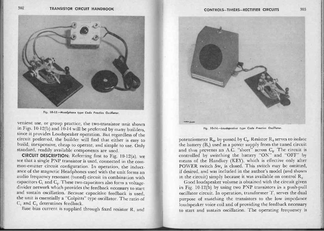
;(1`2 TRANSISTOR CIRCUIT HANDBOOK CONTROLS-TIMERS-RECTIFIER CIRCUITS 303
Fig. 10-13.-Headphone type Code Practice Oscillator.
venient use, or group practice, the two -transistor unit shownin Figs. 10-12(b) and 10-14 will be preferred by many builders,since it provides Loudspeaker operation. But regardless of thecircuit preferred, the builder will find that either is easy tobuild, inexpensive, cheap to operate, and simple to use. Onlystandard, readily available components are used.
CIRCUIT DESCRIPTION: Referring first to Fig. 10-12(a), wesee that a single PNP transistor is used, connected in the com-mon -emitter circuit configuration. In operation, the induct-ance of the magnetic Headphones used with the unit forms anaudio frequency resonant (tuned) circuit in combination withcapacitors C1 and C2. These two capacitors also form a voltage-
divider network which provides the feedback necessary to startand sustain oscillation. Because capacitive feedback is used,the unit is essentially a "Colpitts" type oscillator. The ratio ofC, and C2 determines feedback.
Base bias current is supplied through fixed resistor R1 and
Fig. 10-14.-Loudspeaker type Code Practice Oscillator.
potentiometer R2, by-passed by C3. Resistor R3 serves to isolatethe battery (B1) used as a power supply from the tuned circuitand thus prevents an A.C. "short" across C2. The circuit iscontrolled by switching the battery "ON" and "OFF" bymeans of the Handkey (KEY), which is effective only afterPOWER switch Sw1 is closed. This switch may be omitted,if desired, and was included in the author's model (and shownin the circuit) simply because it was available on control R2
Good loudspeaker volume is obtained with the circuit givenin Fig. 10-12(b) by using two PNP transistors in a push-pulloscillator circuit. In operation, transformer T1 serves the dual
purpose of matching the transistors to the low impedanceloudspeaker voice coil and of providing the feedback necessaryto start and sustain oscillation. The operating frequency is

304 TRANSISTOR CIRCUIT HANDBOOK CONTROLS -TIMERS -RECTIFIER CIRCUITS 305
determined by the transformer used and by the sizes of baseresistors R, and R2, serving both to establish base bias currentand to determine the ratio of the feedback signal. A furthercontrol on frequency is provided by capacitor C which maybe switched across the transformer's primary winding by SPSTswitch Sw,, effectively changing its "natural" resonant fre-quency. Power is supplied by a single battery (B,), controlledby the Handkey (KEY). This circuit, like the first, also usesthe common -emitter circuit configuration, even though thetransistors are connected for push-pull operation.
PARTS LIST - Fig. 10-12(a):R, - 4.7K, 1/2 W. Carbon resistor.R2 - 100K Carbon potentiometer, with switch
(Centralab B -40-S).R3 - 2.2K, 1/2 W. Carbon resistor.C, - 0.02 Mfd., 200 volt, metallized paper capacitor.C2 - 0.05 Mfd., 200 volt, metallized paper capacitor.C3 - 0.1 Mfd., 200 volt, metallized paper capacitor.Sw, - SPST switch (on R2).B, -3 to 6 volt battery (penlight cells in series).Transistor - (1) GE type 2N107.MISC. - Transistor socket; control knob; small metal case
(ICA No. 29435); (4) binding posts; terminal strips; Ma-chine screws, nuts, wire, solder, Misc. Hdwe., etc.
ACCESSORIES - Handkey; Magnetic Headphone(s)1000 to 2000 ohms impedance.
PARTS LIST - Fig. 10-12(b):RR2 -1/2 W. Carbon resistors (see text for values).C, - Tone control capacitor, optional (see text).Ti - Transistor Push -Pull Output transformer
(Argonne No. AR -119).B, -9 volt battery (RCA VS300).PM SPKR - 3" Loudspeaker, 3.2 ohm voice coil.Transistors - (2) Raytheon CK722.MISC. - (2) Transistor sockets; (2) binding posts; small
chassis; battery clips; small cabinet (ICA No. 3996); ter-minal strips; Machine screws, nuts, wire, solder, Misc.Hdwe., etc.
ACCESSORY - Handkey.CONSTRUCTION HINTS: The author's models, shown in Figs.
10-13 and 10-14, should serve to suggest typical constructionto a prospective builder. Relatively few parts are used ineither the Headphone or the Loudspeaker model, so the basiccircuits may be assembled in quite small metal or plastic boxes.In the case of the Loudspeaker model, shown in Fig. 10-14,the size of the loudspeaker used will probably be the deter-mining factor on case size . . . if a 3" loudspeaker is used, astandard Meter Case (specified in the PARTS LIST) makesan attractive housing. Neither parts arrangement or lead dressare critical, so the builder can follow his own inclinations re-garding layout.
If the Headphone model is assembled (Figs. 10-12(a) and10-13), the frequency of operation may be changed by chang-ing capacitors C, and C2. In rare instances it may be necessaryto change component values in this circuit to obtain optimumoperation with the particular pair of Headphones employed.And, of course, other PNP transistors may be used if compo-nent values are adjusted for best operation.
Assembly of the Loudspeaker C.P.O., shown in Figs.10-12(b) and 10-14, requires that certain values be determinedexperimentally. First, base resistors R, and RZ are chosen togive the best compromise between desired tone and outputvolume. These two resistors should have the same value. Theymay be determined either by using a rheostat in each circuitor temporarily connecting a Resistance Substitution Box inplace of the resistors. Typical values should fall between 10Kand 100K. If two output frequencies are required, C, may beadded to the circuit. Again, this value is determined experi-mentally for the tone desired . . . typical values run between0.001 and 0.02 Mfd.
Regardless of which model is assembled, the transistors andbattery should not be installed until after all wiring has been

306 TRANSISTOR CIRCUIT HANDBOOK CONTROLS -TIMERS -RECTIFIER CIRCUITS 307
double-checked for possible errors and accidental shorts. Ifdesired, NPN transistors with similar gain characteristics maybe used in either circuit, provided battery polarities are re-versed.
LIGHT BEAM RECEIVER: The "dits" (dots) and "dahs"(dashes) of the International Morse Code may be transmittedboth as an interrupted Radio Signal and as a flashing LightBeam. Generally speaking, faster communication is possiblewith Radio than with Light, however, since the average trainedoperator can recognize and record messages which he hears astones faster than he can recognize and record messages re-ceived as flashing lights. But if the instrument shown in Fig.10-15 is used, Light Beam signals can be received as audiotones.
This instrument, which employs two transistors and a selen-ium photocell, converts light into an audio signal which canbe heard in the Headphone. The frequency of the audio signalproduced depends, to some extent, on the intensity of the lightbeam striking the photocell. This fact permits the unit to beused as an Audible Light Meter in addition to its applicationas a Light Beam Receiver. A switch is provided to cut out the"tone generation" characteristic, permitting it to be used to
2N34 2N35RS-3.3K
Fig. 10 -15. --Circuit for a Light Beam Receiver or Audio Photometer.
receive modulated light, thus increasing its versatility evenfurther.
CIRCUIT DESCRIPTION: Referring to the schematic diagram(Fig. 10-15), the Light Beam Receiver uses a type 2N34 and atype 2N35 NPN transistor in a modified direct -coupled com-plementary amplifier circuit. The common -emitter configura-tion is used in both stages. The basic amplifier is convertedinto an audio frequency multivibrator by feedback betweenthe "output" and "input" circuits through capacitor C1, con-trolled by switch Sw1.
In operation, oscillation is prevented by a "reverse" biasapplied to the base of the first (PNP) stage. This bias currentis obtained from battery B1, with voltage divider R3 -R4 deter-mining the exact bias level. The self -generating seleniumphotocell PC, is also connected to the base -emitter circuit, butwith a polarity which tends to cancel the bias current suppliedthrough R2. Thus, when light strikes the photocell, the cur-rent produced by it cancels the bias and allows oscillation totake place . . . this is heard as a tone in the Headphone servingas the collector load for the second (NPN) stage.
Unby-passed emitter resistors R1 and R2 are included toimprove circuit stability and to increase the input impedancesof their respective stages. Interstage coupling resistor R5, by-passed by C2, is included to limit maximum current betweenstages and thus to protect the transistors; other than servingfor current limiting purposes, R5 (and C2) is not essential tocircuit operation. Power is supplied by B2, controlled by SPSTswitch Sw2.
PARTS LIST:R1, R2 - 39 ohm, 1/2 W. Carbon resistors.R3 - 1 Megohm Carbon potentiometer (Centralab B-69).R4 - 10K, 1/2 W. Carbon resistor.R, - 3.3K, I/2 W. Carbon resistor.C, - 0.001 Mfd. disc ceramic (Centralab DD -102) . . .
see text.- 16 Mfd., 12 volt electrolytic (Barco No. P12-16).
Sw1, Sw2 - SPST Toggle switches.
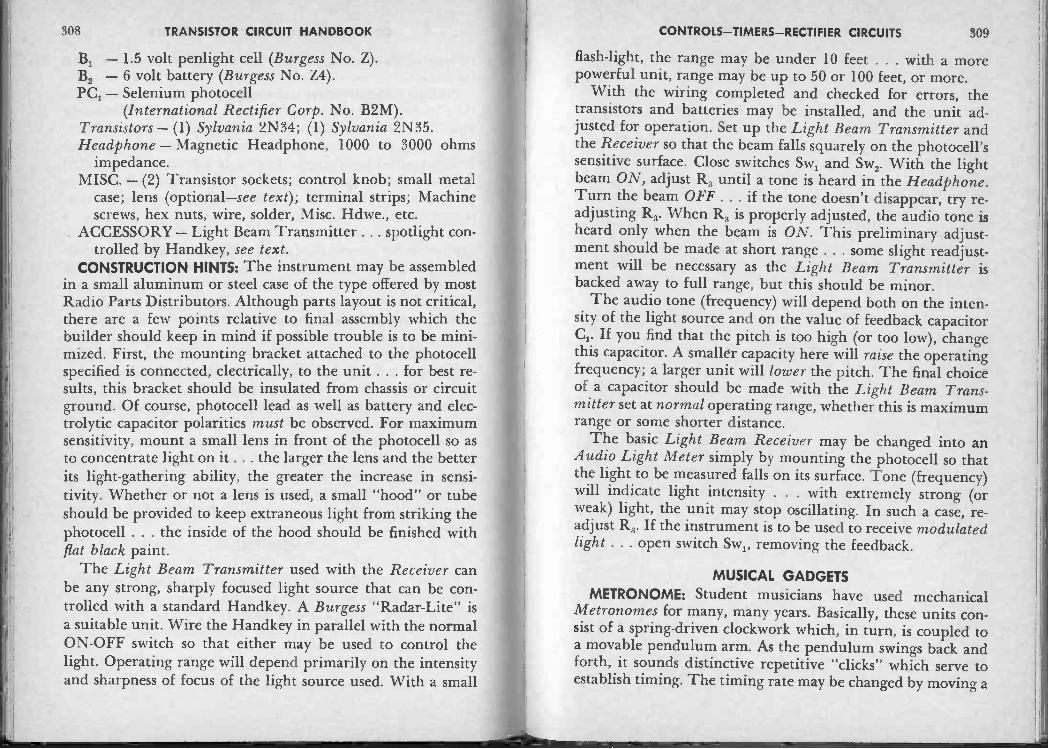
308 TRANSISTOR CIRCUIT HANDBOOK CONTROLS -TIMERS -RECTIFIER CIRCUITS 309
B1 - 1.5 volt penlight cell (Burgess No. Z).B2 6 volt battery (Burgess No. Z4).PC,- Selenium photocell
(International Rectifier Corp. No. B2M).Transistors - (1) Sylvania 2N34; (1) Sylvania 2N35.Headphone - Magnetic Headphone, 1000 to 3000 ohms
impedance.MISC. - (2) Transistor sockets; control knob; small metal
case; lens (optional-see text); terminal strips; Machinescrews, hex nuts, wire, solder, Misc. Hdwe., etc.
ACCESSORY - Light Beam Transmitter . . . spotlight con-trolled by Handkey, see text.
CONSTRUCTION HINTS: The instrument may be assembledin a small aluminum or steel case of the type offered by mostRadio Parts Distributors. Although parts layout is not critical,there are a few points relative to final assembly which thebuilder should keep in mind if possible trouble is to be mini-mized. First, the mounting bracket attached to the photocellspecified is connected, electrically, to the unit . . . for best re-sults, this bracket should be insulated from chassis or circuitground. Of course, photocell lead as well as battery and elec-trolytic capacitor polarities must be observed. For maximumsensitivity, mount a small lens in front of the photocell so asto concentrate light on it . . . the larger the lens and the betterits light -gathering ability, the greater the increase in sensi-tivity. Whether or not a lens is used, a small "hood" or tubeshould be provided to keep extraneous light from striking thephotocell . . . the inside of the hood should be finished withflat black paint.
The Light Beam Transmitter used with the Receiver canbe any strong, sharply focused light source that can be con-trolled with a standard Handkey. A Burgess "Radar-Lite" isa suitable unit. Wire the Handkey in parallel with the normalON -OFF switch so that either may be used to control thelight. Operating range will depend primarily on the intensityand sharpness of focus of the light source used. With a small
flash -light, the range may be under 10 feet . . . with a morepowerful unit, range may be up to 50 or 100 feet, or more.
With the wiring completed and checked for errors, thetransistors and batteries may be installed, and the unit ad-justed for operation. Set up the Light Beam Transmitter andthe Receiver so that the beam falls squarely on the photocell'ssensitive surface. Close switches Sw1 and Sw2. With the lightbeam ON, adjust R3 until a tone is heard in the Headphone.Turn the beam OFF . . . if the tone doesn't disappear, try re-adjusting R3. When R3 is properly adjusted, the audio tone isheard only when the beam is ON. This preliminary adjust-ment should be made at short range . . . some slight readjust-ment will be necessary as the Light Beam Transmitter isbacked away to full range, but this should be minor.
The audio tone (frequency) will depend both on the inten-sity of the light source and on the value of feedback capacitorC1. If you find that the pitch is too high (or too low), changethis capacitor. A smaller capacity here will raise the operatingfrequency; a larger unit will lower the pitch. The final choiceof a capacitor should be made with the Light Beam Trans-mitter set at normal operating range, whether this is maximumrange or some shorter distance.
The basic Light Beam Receiver may be changed into anAudio Light Meter simply by mounting the photocell so thatthe light to be measured falls on its surface. Tone (frequency)will indicate light intensity . . . with extremely strong (orweak) light, the unit may stop oscillating. In such a case, re-adjust R3. If the instrument is to be used to receive modulatedlight . . . open switch Sw1, removing the feedback.
MUSICAL GADGETSMETRONOME: Student musicians have used mechanical
Metronomes for many, many years. Basically, these units con-sist of a spring -driven clockwork which, in turn, is coupled toa movable pendulum arm. As the pendulum swings back andforth, it sounds distinctive repetitive "clicks" which serve toestablish timing. The timing rate may be changed by moving a
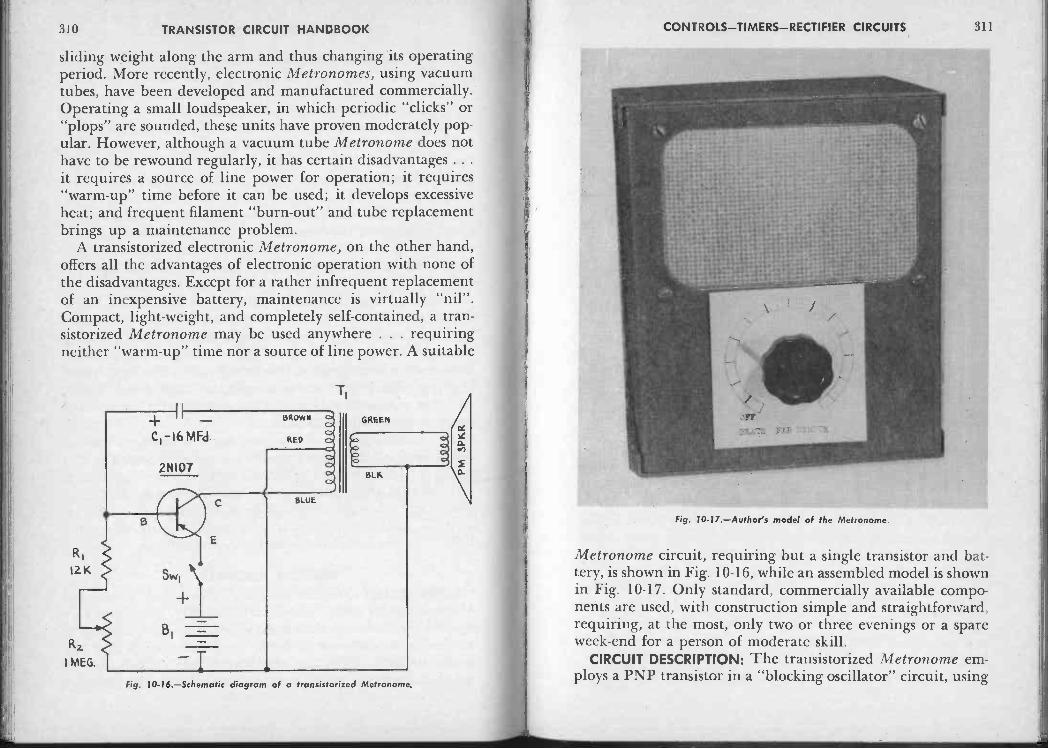
310 TRANSISTOR CIRCUIT HANDBOOK
sliding weight along the arm and thus changing its operatingperiod. More recently, electronic Metronomes, using vacuumtubes, have been developed and manufactured commercially.Operating a small loudspeaker, in which periodic "clicks" or"plops" are sounded, these units have proven moderately pop-ular. However, although a vacuum tube Metronome does nothave to be rewound regularly, it has certain disadvantages . . .
it requires a source of line power for operation; it requires"warm-up" time before it can be used; it develops excessiveheat; and frequent filament "burn -out" and tube replacementbrings up a maintenance problem.
A transistorized electronic Metronome, on the other hand,offers all the advantages of electronic operation with none ofthe disadvantages. Except for a rather infrequent replacementof an inexpensive battery, maintenance is virtually "nil".Compact, light -weight, and completely self-contained, a tran-sistorized Metronome may be used anywhere . . . requiringneither "warm-up" time nor a source of line power. A suitable
+ I -C1-16 M Fd
2N107
R
12K
Rz
I MEG.
SW1
BI
BROviw
RED
BLUE
T
GREEN
O
BLK
Fig. 10-16.-Schematic diagram of a transistorized Metronome.
CONTROLS-TIMERS-RECTIFIER CIRCUITS 311
Fig. 10-17.-Author's model of the Metronome.
Metronome circuit, requiring but a single transistor and bat-tery, is shown in Fig. 10-16, while an assembled model is shownin Fig. 10-17. Only standard, commercially available compo-nents are used, with construction simple and straightforward,requiring, at the most, only two or three evenings or a spareweek -end for a person of moderate skill.
CIRCUIT DESCRIPTION: The transistorized Metronome em-ploys a PNP transistor in a "blocking oscillator" circuit, using

312 TRANSISTOR CIRCUIT HANDBOOK
the common -emitter configuration. Power is supplied by asingle battery, B1, controlled by SPST switch Sw,.
In operation, transformer T, serves the dual purpose ofproviding the feedback necessary to start and sustain oscilla-tion and of matching the transistor's high impedance outputto the low impedance of the loudspeaker's voice coil. To ac-complish this dual purpose, a push-pull output transformer isemployed. The repetition rate is determined by the R -C timeconstant of coupling capacitor C, and the base resistor, madeup of fixed resistor R and the "beat rate" control R2. Adjust-ing R2 changes the R -C time constant and thus changes the
operating rate (frequency).
PARTS LIST:
R, - 12K, y2 W. Carbon resistor.R, - 1 Megohm Carbon potentiometer (Centralab B-69).C, - 16 Mfd., 12 volt electrolytic (Barco P12-16).T, - Transistor output transformer
(Argonne No. AR -138).Sw, - SPST switch, on R2.B, -9 volt battery (RCA No. VS300).PM SP KR - 4" PM Loudspeaker, 3.2 ohm voice coil.Transistor - (1) GE type 2N107.MISC. - Transistor socket; control knob; battery clips;
metal case (L.M.B. No. 142); (4) rubber feet; Machinescrews, nuts, wire, solder, Misc. Hdwe., etc.
CONSTRUCTION HINTS: The exterior view of the author'smodel, given in Fig. 10-17, might be used as a guide by theworker assembling his own unit. However, since parts layoutis not at all critical, the builder can follow his own inclina-tions. Even the metal case can be changed, since it is notneeded for shielding purposes . . . a plastic, or even a woodencase is equally satisfactory for housing this circuit. The onlypoints to watch are the transformer connections and the bat-tery (B,) and electrolytic capacitor (C,) lead polarities. OtherPNP transistors may be substituted for the unit specified and,in most cases, no component changes need be made. Even a
CONTROLS -TIMERS -RECTIFIER CIRCUITS 313
NPN transistor may be used, provided the battery and electro-lytic capacitor leads are reversed.
Once the wiring is completed and checked, the transistorand battery should be installed and the instrument tested. Asa final step, the "rate" control (R2) should be calibrated inBeats Per Minute. This may be done by using another Metro-nome as a standard or by actually counting the individualbeats, using a stop watch (or watch with a sweep -second hand)to determine the timing interval.
If the operating range is not satisfactory, it may be changedquite easily by changing capacitor C,. A larger capacitor herewill lower the maximum beat rate, while a smaller unit willgive a higher repetition rate. The minimum rate (frequency)is determined by fixed resistor R, plus the maximum value ofR2; the maximum rate is determined by R, alone, for a givenvalue of C,. If desired, R, may be changed to vary the maxi-mum rate, but, in general, should not be lower than 10K.
"MUSICAL TOYS": Transistors, because of their small size,light weight, ruggedness, and low cost, are almost ideally suitedto the construction of electronic toys. In addition to their de-sirable physical characteristics, their minute power require-ments make battery operation feasible and this, in turn, per-mits the design of a self-contained and completely portabletoy. More important, the use of low battery voltages insurescomplete freedom from possible shock.
A basic approach to electronic toy design is to assemble astandard circuit into a special or "gimmick" package. For ex-ample, one of the Receiver circuits described in Chapter 8might be assembled as a Wrist Radio, Spaceman's Set, orPolice Receiver, depending on the housing used. Using thisapproach, a "Musical" type of toy might be developed arounda simple audio oscillator driving a loudspeaker. By changingthe housing, the same circuit might become, in turn, a Banjo,an Organ, a Violin, a Guitar or almost any other type of elec-tronic toy. Typical circuits that might be used in such applica-tions are given in Fig. 10-18, while an assembled electronicBanjo is shown in Fig. 10-19.
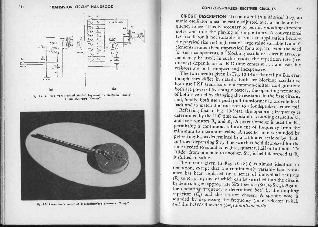
311 TRANSISTOR CIRCUIT HANDBOOK CONTROLS-TIMERS-RECTIFIER CIRCUITS 315
IN AR
WO.RIO
C K722
017181
SAC
Rz- 50K
Ken
nASPKA
I
52"17, C.-0.0170 0.1 BOIL
R 3BAN
2N109
Sv-13,
112
TI
pR
(a) (b)
Fig. 10-18.-Two transistorized Musical Toys-(a) an electronic "Banjo";(b) an electronic "Organ".
Fig. 10-19.-Author's model of a transistorized electronic "Banjo".
CIRCUIT DESCRIPTION: To be useful in a Musical Toy, anaudio oscillator must be easily adjusted over a moderate fre-quency range. This is necessary to permit sounding differentnotes, and thus the playing of simple tunes. A conventionalL -C oscillator is not suitable for such an application becausethe physical size and high cost of large value variable L and Celements render them impractical for a toy. To avoid the needfor such components, a "blocking oscillator" circuit arrange-ment may be used; in such circuits, the repetition rate (fre-quency) depends on an R -C time constant . . . and variableresistors are both compact and inexpensive.
The two circuits given in Fig. 10-18 are basically alike, eventhough they differ in details. Both are blocking oscillators;both use PNP transistors in a common -emitter configuration;both are powered by a single battery; the operating frequencyof both is varied by changing the resistance in the base circuit;and, finally, both use a push-pull transformer to provide feed-back and to match the transistor to a loudspeaker's voice coil.
Referring first to Fig. 10-18(a), the operating frequency isdetermined by the R -C time constant of coupling capacitor C1and base resistors R1 and R2. A potentiometer is used for R2,permitting a continuous adjustment of frequency from theminimum to maximum value. A specific note is sounded bypre-setting R0, as determined by a calibrated scale or by "feel"and then depressing Swi. The switch is held depressed for thetime needed to sound an eighth, quarter, half or full note. To"slide" from one note to another, Swi is held depressed as R2is shifted in value.
The circuit given in Fig. 10-18(b) is almost identical inoperation, except that the continuously variable base resist-ance has been replaced by a series of individual resistors(R1 to R10), any one of which can be switched into the circuitby depressing an appropriate SPST switch (Sw2 to Sw,i). Again,the operating frequency is determined both by the couplingcapacitor (C1) and the resistor chosen. A specific note issounded by depressing the frequency (note) selector switchand the POWER switch (Swi) simultaneously.

316 TRANSISTOR CIRCUIT HANDBOOK
PARTS LIST - Fig. 10-18(a):R, - 6.8K, '/2 W. Carbon resistor.R2 - 50K Carbon potentiometer (Centralab B-31).Ci - 0.25 Mfd., 200 volt tubular paper capacitor.T, - Audio output transformer (Merit A-2900).Swi - SPST Push-button switch, normally open.B, - 221/2 volt Hearing Aid battery (Burgess No. U-15).PM SPKR - 4" to 6" PM Loudspeaker, 6-8 ohm voice coil.Transistor - (1) Raytheon CK722.MISC. - Transistor socket; battery box (Austin -Craft No.
113); Bar knob or control lever; housing (see text); ter-minal strips; Machine screws, nuts, wire, solder, Misc.Hdwe., etc.
PARTS LIST - Fig. 10-18(b):R, - Rio -1/2 Watt Carbon resistors (see text).C, - 200 volt paper capacitor
(0.01 Mfd. to 0.1 Mid., see text).Sw,- Sw- SPST Push-button switches, normally open.B, -9 volt battery (RCA VS300).Ti - Transistor output transformer
(Argonne No. AR -139).PM SPKR - 4" to 8" PM Loudspeaker, 8 ohm voice coil.Transistor- (1) RCA 2N109.MISC.-Transistor socket; battery clips; housing (see text);
Machine screws, nuts, wire, solder, Misc. Hdwe., etc.CONSTRUCTION HINTS: Except for the usual care to observe
battery polarity and to avoid overheating transistor leads, nospecial precautions need be observed when assembling eitherof the circuits shown in Fig. 10-18. Neither parts layout norwiring arrangement are critical. More important than thewiring technique employed is the type of housing and rugged-ness of assembly . . . all components and leads should be secureto prevent damage from the bouncing and jiggling which atoy is likely to receive; and the circuit itself should be wellcovered by the housing, to keep out prying and inquisitivefingers.
CONTROLS -TIMERS -RECTIFIER CIRCUITS 317
The type of housing chosen, as well as its material of con-struction, will depend on the type of instrument to be simu-lated by the toy. Metal, wood, or plastic are all suitable for thehousing, provided a reasonably rugged construction is em-ployed. The circuit given in Fig. 10-18(a) is best for toys whichsimulate instruments providing a more or less continuousvariation of tone . . . in general, most string and wind instru-ments. Typical housings might simulate a violin, a banjo, acello, a guitar, or any similar instrument. The circuit given inFig. 10-18(b), on the other hand, is best suited for toys whichsimulate key -operated instruments, such as pianos, organs, oraccordions.
A toy electronic banjo, using the circuit given in Fig.10-18(a), is shown in Fig. 10-19. This home-made instrumentwas assembled from a round cake pan and a length of alumi-num tubing, painted, then decorated with commercial decals.The control switch (Swi) is mounted near the end of the arm,while the tone control (R2) is operated by a control lever. Apattern of small holes were made in the pan for the loud-speaker. In use, this toy is held like a conventional banjo, withone hand operating the push-button and the other adjustingthe frequency control.
Since the circuit given in Fig. 10-18(a) provides a continu-ous control of frequency, any note within its range may besounded by adjusting R2. The circuit given in Fig. 10-18(b),on the other hand, depends on fixed resistors to determine in-dividual notes (R, to R10) . . . although ten resistors are speci-fied, any number may be used, depending on the number ofnotes required. These resistor values are determined experi-mentally to give the desired note with the particular couplingcapacitor (C,) employed. Typical values range from 12K toabout 220K. Capacitor C, is chosen to place emphasis on eitherthe low-pitched or the high-pitched notes . . . the larger Cthe lower the operating frequency, for a given base resistance.
GENERAL SEMICONDUCTOR APPLICATIONSAs discussed in the INTRODUCTION (Chapter 1), tran-

318 TRANSISTOR CIRCUIT HANDBOOK CONTROLS-TIMERS-RECTIFIER CIRCUITS 3 1 9
sistors are a group within a general class of semiconductorcomponents, with the larger class including diodes, photocells,and other types of devices. Thus far, we have emphasized tran-sistor circuits; this is proper, of course, in a TRANSISTORCIRCUIT HANDBOOK. Although diodes, photocells, andother semiconductor devices have been shown in a number ofinstrument diagrams, their application was generally inci-dental to the transistor circuitry itself. However, the authorfeels that the treatment of general semiconductor applications,if done briefly, would not be completely out -of -place in thisvolume . . . any more than the treatment of diode, phototube,and thyratron applications would be out -of -place, say, in ageneral volume on vacuum tube circuits. It is with this thoughtin mind, then, that we devote the next few pages to circuitsusing semiconductor devices other than transistors.
Typical circuits are given in Figs. 10-20, 10-21, 10-24, 10-26,and 10-27, while photos of assembled models are shown inFigs. 10-22, 10-23, 10-25, 10-28, and 10-29. In order to keepour discussion of each circuit application brief, we shall usean approach intermediate between that employed in discuss-ing the BASIC CIRCUITS in Part II and the detailed de-scriptions employed in the previous sections and Chapters ofPart III.
RECTIFIER CIRCUITS: A diode is a non-linear device, passingcurrent better in one direction than in the other. This char-acteristic makes it useful as a detector or as a rectifier. In prac-tice, both detector and rectifier circuits are similar in appear-ance, differing primarily' in their specific application and inthe additional components used with the basic diode. A de-tector circuit is generally used either to mix two signals, tomodulate one signal with another, or to separate a modulatedsignal into component parts . . . as, for example, separating theR.F. and A.F. components of a modulated R.F. carrier. Arectifier, on the other hand, is generally used to convert A.C.into pulsating D.C., which, in turn, can be changed into pureD.C. by appropriate filtering.
Typical rectifier circuits are given in Fig. 10-20. In any of
-I-
CI
jZ
4 I
CI +
z
a b
z
d
e f
Fig. 10-20.-Basic semiconductor diode Rectifier circuits: (a) Half -Wave; (b) Full -Wave;(c) Full -Wave Bridge; (d) Voltage -Doubler; (e) Voltage-Tripler; (f) Voltage-Quadrupler.
p.

320 TRANSISTOR CIRCUIT HANDBOOK
the circuits, the diode may be a selenium, germanium, or sili-con power rectifier, or a small signal level diode, either junc-tion or point -contact. These circuits may be applied to lowvoltage, high current, or to high voltage, high current, and tohigh voltage, low current applications, depending on the typeof diode used. If suitable capacitor values are chosen, thesecircuits may also be used as detectors.
Half -wave, full -wave, and full -wave bridge rectifiers areshown in Figs. 10-20(a), 10-20(b), and 10-20(c), respectively.In each case, resistor R, is included for current limiting pur-poses, to protect the diode from a damaging current surge incase the applied A.C. voltage is at a peak when input capacitorC, is discharged. Whether included or omitted in a specificcircuit, this small series resistor (generally less than 100 ohms)should be included as a matter of good engineering practicewherever a low impedance diode feeds a high value capaci-tor. The full -wave bridge rectifier shown in Fig. 10-20(c), al-though requiring more diode elements than the circuit givenin Fig. 10-20(b), offers the advantage that a center -tapped driv-ing source is not needed for full -wave rectification.
Voltage multiplying circuits are given in Figs. 10-20(d),10-20(e), and 10-20(f). These circuits supply a D.C. outputvoltage that is a multiple of the peak applied A.C. voltage.Where a sine wave input is used, the peak applied voltage isapproximately 1.41 times the RMS value. Thus, the voltagedoubler circuit shown in Fig. 10-20(d) supplies a no-load D.C.voltage equal to 2.82 times the applied A.C. voltage; the volt-age tripler circuit shown in Fig. 10-20(e) supplies a D.C. out-put equal to 4.23 times the input; the voltage quadruplershown in Fig. 10-20(f) supplies a D.C. output equal to 5.64times the input.
Referring to Fig. 10-20(d), on one half -cycle of the appliedA.G. voltage, either C, or C2 is charged to peak line voltagethrough its appropriate diode. Discharge, except through theoutput load, is prevented by the high back resistance of thediode. On the succeeding half cycle, the other capacitor issimilarly charged to peak line voltage. As far as the D.C. load
CONTROLS -TIMERS -RECTIFIER CIRCUITS 321
is concerned, the two capacitors, C, and C2 are in series aiding,so that their respective D.C. charges add, resulting in the highoutput voltage.
In the voltage tripler circuit, Fig. 10-20(e) C, and C3 arecharged to peak line voltage on one half cycle. On the next,the charge of C, adds to the line voltage to charge C2, throughits diode, to twice peak line voltage. Thus, C2 is charged totwice line voltage, C3 to line voltage, with the result that theD.C. voltage impressed across the output load is three timesthe peak applied A.C. voltage . . . that is, the sum of the D.C.voltage charges across C2 and C3 in series aiding. The voltagequadrupler, Fig. 10-20(f), operates in much the same manner,with C, and C2 charged to peak line voltage, and the seriesoutput capacitors, C3 and C4, each charged to twice the peakapplied A.C. voltage.
In practice, the useful D.C. output voltage is generally lessthan the maximum possible due to the effect of the D.C. load,except where current requirements are almost negligible . . .
as in Geiger Counter and Cathode Ray applications.In any case, with any of the rectifier circuits shown, a stand-
ard filter network is used between the D.C. Output terminalsindicated and the final load. Where current drains are low,R -C filter networks may be used to reduce ripple content.Where the D.C. drain is heavy, L -C networks are used.
To
CONTROLLED
CIRCUIT
Courtesy Radio & Television News
Fig. 10-21.-Circuit of a Cadmium Sulfide (CdS) Photocell Relay.

TRANSISTOR CIRCUIT HANDBOOK
Fig. 10-22.-Author's model of the CdS Photocell Relay.
CdS PHOTOCELL RELAY: A moderately sensitive Light Con-trolled Relay may be assembled by using a Cadmium Sulfidephotoconductive cell, a D.C. power source, and a sensitiveelectromagnetic relay. A typical circuit is given in Fig. 10-21,while exterior and interior views of an assembled model aregiven in Figs. 10-22 and 10-23, respectively. The entire circuithas been assembled in a small aluminum box, with the photo-cell (PC) itself mounted in a thick rubber grommet. Typicalcomponents are as follows: Line cord and plug; Radio Re-ceptor type 8Y1 selenium rectifier; 5.6K, i/2 W. Carbon re-sistor (R1); Clairex type CL -2 Cadmium Sulfide photocell(PC); 2 Mfd., 200 volt paper capacitor (CO; Potter & Brum-field type SS5D relay, 10,000 ohm coil (RLY); aluminum case,Misc. Hdwe., etc.
CONTROLS -TIMERS -RECTIFIER CIRCUITS
Courtesy Radio 8 Television News
Fig. 10-23.-Interior view of the CdS Photocell Relay.
The resistance of a photoconductive cell varies with theamount of light falling on its sensitive surface. The greater thelight, the lower its resistance. In operation, the diode rectifier,together with R1 and C1, form a simple D.C. power supply.The photocell (PC) and the relay (RLY) are in series acrossthis D.C. source. When the photocell is "dark", its resistanceis high and insufficient current can flow to close the relay.When the photocell is exposed to a moderately strong light,its resistance drops, the current goes up, and the relay closes.
60 CYCLE STROBOSCOPE: The word stroboscope is derivedfrom the Greek words meaning-"twisting or turning around"and "to see or view" . . . literally, an instrument for viewing arotating object. In practice, a stroboscope may be used to ob-serve either rotating or vibrating machinery. It accomplishesthis by apparently "stopping" the motion of the object. An

324 325CONTROLS-TIMERS-RECTIFIER CIRCUITS
8YI
TRANSISTOR CIRCUIT HANDBOOK
(a) (b)
:C,- /Us WAG
PROBE I
CE 105
CLIP
GAD LEAD[yLeD51.4]
4,-10A
R, c,MK DOM.
WELDED CASE
R. -120D
(c) (d)
Fig. 10-24.-General semiconductor applications: (a) 60 Cycle Stroboscope;(b) Signal Tracing Probe; (c) Zener Oscillator; (d) Clipper.
electronic stroboscope "stops" motion by illuminating theobject periodically at the same position in its cycle of move-ment. Since the object is always seen in the same position, nomatter how rapidly it is actually moving, it appears to bestanding still.
The circuit for a simple 60 Cycle Stroboscope is given inFig. 10-24(a). This instrument uses a semiconductor device(a diode) to supply pulsating D.C. to a neon bulb, which, inturn, flashes periodically at 60 cycles per second. It may beused to "stop" the motion of rotating or vibrating objectsmoving at this rate (or multiples thereof).
Only four electrical components are required . . . a linecord, a Radio Receptor type 8Y1 selenium rectifier, a 33K,1 W. current limiting resistor (R1), and a type NE -48 neonbulb. The entire instrument is easily assembled in a smallplastic vial. A completed model is shown in Fig. 10-25, alongwith a stroboscopic disk with which it can be used to checkthe speed of record players . . . these small disks are availablefrom most Radio Parts Distributors.
\\0\vollitimi/Ill/l////,N`l.....\\111111///
Fig. 10-25.-A 60 Cycle Stroboscope . . . shown with the disk with which it is used.
SIGNAL TRACING PROBE: Modulated R.F. signals may betraced through a Radio Receiver by using a R.F. Detectortogether with a high gain Amplifier. The circuit for a suitableinstrument is given in Fig. 10-24(b). This Signal TracingProbe features the use of a small Raytheon type CK705 diodeas a detector and incorporates, in its design, a simple R -C filternetwork . . . consisting of R2 and C2. For best results, this in-strument should be assembled in a closed metal tube to pro-vide over-all shielding.
In use, the OUTPUT leads are connected to an AudioAmplifier and the flexible GND. LEAD connected to thechassis of the Receiver under test. The PROBE is touched tothe input and output of various R.F. and I.F. stages in theReceiver to check for the presence of a signal at these points,as well as its relative amplitude. If used on an A.C.-D.C. re-ceiver, an isolation transformer should be employed betweenthe Receiver and the line receptacle to avoid accidental shocks.
ZENER OSCILLATOR: When a D.C. voltage is applied to adiode in its non -conducting direction, very little current willflow until the applied voltage reaches a specific value. At thispoint, a type of "break -down" occurs, and the reverse currentflow will increase appreciably. The voltage at which this con-

326 TRANSISTOR CIRCUIT HANDBOOKCONTROLS-TIMERS-RECTIFIER CIRCUITS 327
dition occurs is called the Zener voltage. This characteristicmay be utilized in a simple relaxation oscillator. A suitablecircuit is shown in Fig. 10-24(c).
The Zener Oscillator requires a D.C. power supply, madeup from a small selenium rectifier (Radio Receptor type 8Y1),a 47 ohm, 1/2 W. Carbon resistor (R1), and a 20 Mfd., 150 voltelectrolytic capacitor (C1). This power supply may be replacedby a 160 volt battery, if desired. The oscillator portion of thecircuit includes a voltage adjustment potentiometer (R2), a100 ohm, 1/2 W. (R3) limiting resistor, a 0.1 Mfd., 200 voltpaper capacitor (C2), and a type 1N34A germanium diode.The output "Load" may be a moderate impedance pair ofHeadphones (1000 ohm magnetic headset) or a small outputtransformer, and is connected in series with C2. The signalwaveform may be observed by connecting an Oscilloscopeacross C2 . . . the 'scope should have a high impedance input,preferably 5 Megohms or more, to prevent undue loading ofthe circuit.
In operation, the D.C. power supply charges capacitor C2slowly through resistors R2 and R3. As long as the voltageacross the capacitor is less than the Zener voltage of the diode,the diode acts as a high impedance . . . almost an open circuit.As soon as the voltage across C2 approaches the Zener voltage,the diode acts like a low impedance device, passing a com-paratively heavy current, and discharging C2. When the volt-age across C2 drops sufficiently, due to its being discharged,the diode again becomes a high impedance device, and thecharging action starts again. The frequency of operation de-pends on the value of C2, on the available voltage, on the indi-vidual diode used, and on the value of the series resistors, R2and R3.
When using this circuit, set R2 at its maximum value, re-ducing it slowly until the circuit breaks into oscillation. Thenturn it back slightly from this point. The Zener Oscillator maybe used as a simple audio oscillator for demonstration pur-poses, for code practice, or as a signal source. It is not suitablefor continuous use, however, for extended operation of the
diode at its Zener voltage rating will result in permanentdamage.
SIGNAL CLIPPER: When a voltage is applied to a diode inits conducting direction, its acts like a very low resistance.This characteristic may be used to "clip" the peaks of an ap-plied signal. A typical circuit is shown in Fig. 10-24(d). Re-ferring to this diagram, almost any diodes may be used in thecircuit . . . suitable types are Raytheon's CK705 and 1N66 orSylvania's 1N34; batteries B1 and B2 set the "clipping" level. . . normally, single penlight cells will be used here. ResistorsR1 and R2 may be 1/2 W. Carbon units.
In operation, an applied A.C. signal is clipped at the voltagelevel determined by batteries B1 and B2. Considering, first, thenegative half -cycle of the applied signal, there is no attenua-tion of the signal, except that caused by the voltage -divideraction of R1 and R2, until the signal level exceeds the voltageof B1. Up to this point, the first diode is biased in its non -con-ducting region. When the applied signal voltage becomesgreater than B1, the diode can conduct and acts like a low re-sistance, forming a voltage -divider with fixed resistance R1and sharply attenuating the signal. The second diode is non-conducting during this period due to the polarity of the ap-plied signal; on the positive half -cycle, however, the first diodedoes not conduct, and the second diode (biased by B2) acts as aclipper. If only one side of the applied A.G. signal is to beclipped, the appropriate diode (and its biasing battery) maybe left out of the circuit. To clip only the negative half -cycle,remove the second diode; to clip only the positive half -cycle,remove the first diode . . . the remaining diode is left in eithercase. If clipping is desired at the "zero" signal level, the biasingbattery may be removed, and the diode connected directlyacross the line.
R.F. APPLICATIONS: A bridge modulator circuit is shownin Fig. 10-26(a). Four R.F. diodes are used . . . Raytheon typeCK705 diodes are satisfactory. This unit may be used to com-bine an audio (A.F.) and a radio (R.F.) signal to provide aModulated R.F. output. The A.F. signal is fed into the circuit

328 TRANSISTOR CIRCUIT HANDBOOKCONTROLS-TIMERS-RECTIFIER CIRCUITS 329
A.F.
REC.
C,- .0005 PAU
R.F.
655.
cx
.001 MFd.
S
(a) (b)
Fig. 10-26.-R.F. Semiconductor Diode applications: (a) Bridge Modulator;(b) Simple Crystal Receiver.
through a small R.F. choke (R.F.C.) . . a typical value is 2.5MHy (Superex No. F-25). The R.F. signal is coupled into thecircuit through a small mica or ceramic capacitor (C1-0.0005Mfd.), which serves to block the A.F. signal. The modulatedoutput is obtained through a 0.001 Mfd. ceramic capacitor(C2). A typical application of this circuit would be to combinean R.F. signal from a small R.F. Signal Generator (such as theunit shown in Chapter 9, Fig. 9-4) with the output from anAudio Oscillator (such as the unit shown in Chapter 9, Fig.9-1) to provide a Modulated R.F. signal. The circuit may beassembled in a small metal box and used as an accessory withother instruments . . . or it may be used as a "built-in" featureof another piece of equipment.
A simple crystal receiver is shown in Fig. 10-26(b). Since nogain is provided, a good antenna and ground system must beused with the unit. Tuning coil L, and variable capacitor C,are chosen to cover the desired frequency range. Capacitor C,,a 0.001 Mfd. mica or ceramic unit, is used as a simple R.F.
(a)
KED
(b)TO CONTROLIA0 CA
(c)'CELLO., (d)
Fig. 10-27.-Semiconductor diode Relay and Mete applications: (a) Sensitive A.C. Relay;(b) Polarized Relay; (c) A.C. Meter; (d) Meter Protection Circuit.
filter. Best results are obtained when high impedance mag-netic headphones are used in this circuit. In this application, asemiconductor diode serves as a simple R.F. detector.
RELAY CIRCUITS: Typical semiconductor diode applicationsto relay circuits are illustrated in Figs. 10-27(a) and 10-27(b).In Fig. 10-27(a), a bridge rectifier is used to convert a D.C.unit into an A.C. Relay. Separate diode elements may be usedto make up the assembly or, if preferred, a pre -assembled"bridge" instrument rectifier may be used. A suitable type isthe Conant Series 500, Type M. This circuit arrangement isoften used with sensitive relays, such as the Advance typeSV/1C.
If a diode is connected in series with a D.C. relay, as shownin Fig. 10-27(b), the assembly becomes a Polarized Relay. Thatis, the relay will work on either A.G. or on D.C. of the correctpolarity. Such a circuit permits two different relays to be con-trolled independently over the same line. A diode is connectedso that one operates with a positive voltage, as shown in the

330 TRANSISTOR CIRCUIT HANDBOOK CONTROLS-TIMERS-RECTIFIER CIRCUITS 331
diagram. A reversed diode is used with the second relay, per-mitting its operation on a negative voltage only. By applyingthe proper voltage to the line, either relay may be closed atwill . . . or both may be closed simultaneously by applying anA.C. voltage. This general arrangement is quite popular incertain types of remote control work.
METER APPLICATIONS: Semiconductor diodes are oftenused as rectifiers to permit the operation of D.C. Meters onA.C. Almost any of the basic rectifier circuits given in Fig.10-20 may be used, but the bridge circuit is probably the mostpopular. This arrangement is shown in Fig. 10-27(c). Themeter (M) is connected directly across the bridge and, often,is by-passed with a small capacitor (C1) to minimize ripple.This capacitor is more important at low frequencies, but, onoccasion, may be used in R.F. work. Typical values, at powerfrequencies and A.F. are .05 to 1.0 Mfd., at R.F. from .001 to.02 Mfd. Either four individual diodes or a single bridge rec-tifier assembly may be used. Typical units are the ConantSeries 500, Type M, Series 160, Type B, and the Series 160-C,Type B -C, or the Bradley Types CX2E4U and CX4D4U.
An interesting application for a shunt diode is shown inFig. 10-27(d), where a semiconductor diode is connected inparallel with a basic meter movement (M). The diode is one ofa series of Meter Protection Diodes developed by The Inter-national Rectifier Corporation (1521 East Grand Ave., ElSegundo, California). These units are designed to protect rela-tively sensitive meters against accidental overloads. In opera-tion, they exhibit a very high resistance within the meter'scalibrated range, but have a comparatively low resistancewhen the voltage drop across the meter (due to current flowthrough it) passes a certain minimum value, acting to shunt,and to protect, the movement.
SUN BATTERIES: The "self -generating" photocells specifiedin a number of earlier projects are, in reality, low power SunBatteries . . . that is, semiconductor devices capable of convert-ing light energy into electrical power. Many semiconductormaterials exhibit these photoelectric characteristics, but the
Fig. I0 -28.--A single selenium Photocell.
majority of commercial Sun Batteries are manufactured fromeither silicon or selenium. A typical selenium cell is shown inFig. 10-28.
Silicon cells are offered by a number of manufacturers, butone of the leading suppliers of "across -the -counter" unitswhich experimenters and gadgeteers may be able to obtain anduse is NATFAB (National Fabricated Products, 2650 WestBelden Avenue, Chicago 47, Illinois). Their type S-1 cell, around unit approximately 11/2" in diameter, can supply up to10 milliwatts in full sunlight under optimum conditions.
Selenium photocells have been available commercially muchlonger than silicon units and have been used for many yearsin Photographers' Exposure Meters. A leading producer ofunits for experimenters is The International Rectifier Cor-poration (1521 East Grand Ave., El Segundo, California).Their popular type B2M unit, with an active area of approxi-mately 0.26 square inches, will develop as much as 0.5 voltsunder "no-load" conditions in average sunlight, or will drive

332 TRANSISTOR CIRCUIT HANDBOOK
Fig. 10-29.-Easily assembled "Sun Battery" . . . will power a simple receiver, an audioamplifier, or a Code Practice Oscillator, or even a low -power transmitter in full sunlight.
a current of 2.0 MA through a 10 ohm load under similarconditions.
Where greater currents, or voltages, are required than canbe delivered by a single cell, whether silicon or selenium,groups of cells may be mounted in "batteries" and connectedin series or parallel combinations. A series arrangement is usedto obtain higher voltages, a parallel arrangement to obtainhigher currents, and a series -parallel arrangement where bothhigher voltages and currents are needed. A typical bank, orbattery, of photocells is shown in Fig. 10-29; six InternationalRectifier type B2M units are used, with their leads brought toindividual terminals, permitting a choice of either series, par-allel, or series -parallel connections, as needed for a particularexperiment. Large banks of Sun Batteries can supply sufficient
power to operate small motors.
CONTROLS-TIMERS-RECTIFIER CIRCUITS 333
Because transistors require so little power for operation, itis only natural to think of combining a transistorized circuitwith a Sun Battery power supply. This is a fairly easy job toaccomplish, for many of the receiver, amplifier, and oscillatorcircuits given in the last few Chapters may be powered by oneor more Sun Batteries. In most cases, it is only necessary toadjust component values (generally the base resistors) for op-timum operation.
The experimenter choosing a Sun Battery may be guidedby both electrical specifications and economic considerations.At this writing, silicon units are much more efficient thanselenium units having the same sensitive area, but are many,many times more expensive. For commercial and militaryapplications, where efficiency, ruggedness, and similar factorsare of prime importance, and economic considerations of sec-ondary interest, silicon units will probably be preferred. Butthe home hobbyist, with his pocketbook and budget to con-sider, will probably prefer to work with the selenium photo-cells.
CONCLUSIONWith the end of this Chapter, we reluctantly conclude Part
III and our discussion of practical transistor Circuit Applica-tions. Throughout the four Chapters making up Part III, wehave attempted to describe a wide variety of equipment cir-cuits, not only to supply the experimenter, gadgeteer, student,Ham, and home -builder with actual construction information,but, in a larger sense, to illustrate how the many, many BasicCircuits discussed in Part II could be applied to every -dayequipment design. At the risk of being repetitious, we havedescribed each equipment circuit as a more or less independ-ent "project". While this has certainly called for some slightduplication of material, particularly in the CONSTRUC-TION HINTS, we feel that the advantages to this approachfar outweigh any possible disadvantages that might accrue.We have felt that the average reader would prefer to have thevarious circuits arranged and described in "project" fashion,for it permits him to refer to those equipments which are of
334 TRANSISTOR CIRCUIT HANDBOOK
especial interest to him without the need of reading throughan entire Chapter or section. As mentioned earlier, the authorintends that this volume shall serve as a true Handbook ratherthan as a text or "story".
Again, we must repeat that the reader should consider theseconstruction projects in the same light that the earlier circuitswere described . . . that is, as a guide to transistor application,rather than as a complete listing. He should not hesitate toadapt the circuits to his own special needs, nor to work upcompletely new circuits, based on combinations and modifica-tions of both the Basic Circuits given in Part II and projectsdescribed in this section (Part III).
PART IV - REFERENCE DATA
Introduction to PART IV
There are a number of topics which are useful to transistorcircuit design and test but which cannot be classified as cir-cuit information. Such topics include data on transistorcharacteristics, definitions of technical terms, basic designformula, laboratory techniques and related supplementaryinformation. For the convenience of the reader, all of thesetopics, except those the author felt would be more helpful asintroductory material, have been grouped together in PARTIV (Reference Data). The introductory topics were discussedin PART I (Laboratory Practice). Like the circuit data givenin PARTS II and III, the reference material in PART IV isnot intended to be read as a novel nor studied as a textbook.Rather, the technical data should be referred to as needed.
The material in PART IV has been divided into fourrelatively independent chapters. Chapter 11 covers TransistorCharacteristics and is based partially on material abstractedfrom a chart appearing in a well known trade publicationand partially on material obtained by the author in responseto inquiries sent to every known transistor manufacturer.Chapter 12 covers basic Definitions and Design Formulas.Of necessity, the amount of design information given hasbeen limited, in keeping with the stated purpose of this vol-ume. The author feels that detailed design information fallsmore within the provinces of textbooks and Design Manuals.Chapter 13 covers Special Techniques not discussed else-where as well as New Developments in the field. In referringto Chapter 13, the reader should remember that the art isstill in a highly fluid state, with new developments announcedby research laboratories and manufacturers almost on a day-to-day schedule. In a semi -permanent work like this volume,
335

336 TRANSISTOR CIRCUIT HANDBOOK
as contrasted to a monthly publication, it is possible to coveronly those developments which have crystallized sufficientlyto permit examination and discussion. For the latest informa-tion on new developments in the field, the reader should usethe material discussed in Chapter 13 as supplemental to ma-terial found in current issues of the various trade publica-tions, professional journals, and popular technical magazines.
A portion of the material in PART IV, especially the in-formation dealing with techniques and new developments inChapter 13, was touched upon briefly in PART I of this vol-ume. The author felt that a more exhaustive treatment ofthe subject matter would have been out -of-place in PART I,but that a more detailed discussion was desirable in view ofthe state of the art. Hence the inclusion of the material onprinted circuits, on a transistor tester, and on "field effect"transistors in Chapter 13.
Finally, Chapter 14 is a basic Bibliography, included forthe convenience of the reader in obtaining more detailed in-formation on specialized topics. A few words concerning theBibliography may be in order. The author makes no claimthat the listing of sources is complete or exhaustive. A com-plete bibliography of all available transistor and semiconduc-tor literature could easily fill a volume. Moreover, such a
complete listing would duplicate existing information, formost of the subject papers that could be listed have alreadybeen listed in other, easily available, bibliographic works.Therefore, in the interests of conserving space, the authorhas tried to limit the bibliography to those technical papers,books, and magazine articles which he found especially help-ful. However, he has included a listing of all transistor biblio-graphic and reference lists with which he is familiar. Most ofthese lists are currently available. The reader planning ex-haustive literary research on any phase of transistor workwill find it worthwhile to consult copies of the bibliographicworks listed.
TRANSISTOR -CHARACTERISTICS -MANUFACTURERS 337
In addition to books, magazines, professional journals, andsimilar conventional sources of circuit data, a good deal ofvaluable reference material will be found in the literaturepublished by transistor and component manufacturers. Someof this material is in the form of reprints of technical papersand magazine articles originally written by members of themanufacturers' staff. However, considerable original materialis available and the reader is advised to check such sourcesfor circuit suggestions and application data relative to specifictypes or circuit components.
PART IV-REFERENCE DATA
Chapter 11
TRANSISTOR CHARACTERISTICS - MANUFACTURERSSECTION A: Transistor Characteristics
The table given on the following pages lists commerciallyavailable transistors and their characteristics. Transistormanufact"urers are identified by a coded list at the end of thetable. This table has been abstracted from a longer TransistorData Chart appearing originally in the July, 1955 issue ofELECTRONIC DESIGN and is reprinted here with thekind permission of the Copyright holder, the Hayden Pub-lishing Co., Inc., of N. Y. The author has modified the origi-nal Data Chart to some extent, principally by excluding anumber of suppliers given in the earlier list. Before listingany manufacturer as a transistor supplier, the author madea sincere effort to contact that manufacturer, either by per-sonal call, by telephone, or by correspondence. Several of thefirms mentioned in the original list indicated that they wereproducing transistors in experimental quantities only and didnot foresee mass production in the immediate future; on thisbasis, the author did not feel it would be germane to listthem as current suppliers. At least one firm (Radio Receptor)has suspended transistor production temporarily. Another

338 TRANSISTOR CIRCUIT HANDBOOK
firm (Hydro -Aire) sold its transistor manufacturing facilities.Still others failed to respond to correspondence and personalcontacts, thus indicating that they were not actively in busi-ness. The only firms retained in the final list are those whowere in current production and who could deliver sample orproduction quantities of transistors on order.
Due to the present extremely fluid state of the field, anytable listing commercially available transistors and their char-acteristics is obsolete almost before it is published. However,the following table covers the transistor types used in provingout the Basic Circuits given in PART II and the EquipmentCircuits given in PART III of this volume, unless otherwisenoted. Nonetheless, the author hastens to caution the readerto use the following table for general reference only, not asa final guide. For full information on the latest availabletransistor types and their electrical and mechanical specifica-tions, write directly to the manufacturers listed.
The majority of the junction transistors listed are PNPunits. These have no special identification. The NPN tran-sistors are identified by an asterisk (*) next to their typenumber. The column headings at the top of the chart standfor the following parameters:
V, Collector voltage/, Collector currentW, Collector dissipation (Where available, the tem-
perature at which W, was measured is given inparentheses.)
a "alpha" or current amplification factor (listedvalue less unity) .
base current amplification factor (listed valuemore than unity) .
PG Power gainPO Power outputZ Source impedance at which PG and PO measuredRL Load resistance at which PG and PO measuredNF Noise factor
TRANSISTOR-CHARACTERISTICS-MANUFACTURERS 339
Fc0 Cutoff frequencyC Type of circuit for which the characteristics are
listed. "GE" being grounded emitter; "GB" be-ing grounded base; "GC" being grounded collec-tor; "CE" being common emitter connection.
P.-, 010 :8
g.4g
70'
coco
cc
o g0
>4 oo 'EA 5
Ce
EDc m
0 F.E.1.01
'!" `,1e'
D I-
.4 .4ot)0 14
CO
Oco0 4
Co .. 7:,',-,00 01 1-, Z1 p,6 0 vs
3.7. 411 ; V
c 1
6'
-=k3
4 g'- JciZi
<4op a
'' )'
.P., ,I
g 't ,- '4o'::
g o
og,'s0..?,
V
.., g 0 0 irj. 2
ai, a o..a 8;- ,- p48 o, .;:s o
U O- c..) ,;-..: g-N$: -54 ... C)s. ...,--'0 ;F:1 o.""
4 4 fal. g'0 rml`' f:0'
C.)c4"4
ad
02
-1/41
PTI
r
o .
Z.) >-
8
zCO
-
8Q..3
EIv
.C, t.2- II
.II _.- a
71 4.20
0 is,o - .4
ei i.i 5 CI i
ac c ; ec no
Z; VE i 6' i-0
1
E.' acQo'-co TE o .e
rj 0 E o o -oc..7,
nN 00 .0 V
O0. - - fi In-ej
6: NI L 6 . ; I: 1 .. 4..2 e _
DI.
:gt7 1 2L c:I.I.
-c.-0
4- I I et 2,
8 z, . 000_
:7-,
C N0 0CVe",
V il!
igi : -cx
8i
1.1-
: E i 1 II
I 2 i `I g- :t 0 . . ....
in . 0
i_c,:.
.....
..-_i
I I°- . 7, .,, i ,. 0 3 -- -0
s -g .- .a.... ,.,7 ° 0 0 TD :t g -i- . i -1,' 7, .2-. - .g _ 1 .00. .E vii-o.'i'x a22 3 - *- 2 t = - 'T ' = ifr -ot -0 ° "E c0 ." 13 : E 5 7- c :E:.o.-...-:-
.Z :22-te.-iflm-t2<ugo.21-23m17 7; 7; c7 7,70
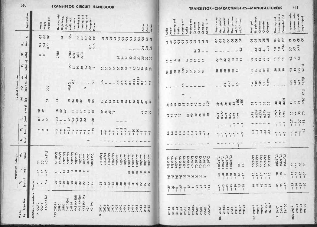
Mad
eB
yT
ype
No.
Max
imum
Rat
ings
Typ
ical
Ope
ratio
nye
(vol
ts)
(ma)
We
(mw
)I°
(ma)
Ve
(vol
ts)
le
(ma)
a or
3P
G
(db)
PO
Zs
RL
(mw
) (k
ilohm
) (k
ilohm
)N
F
(db)
Fe
(Mc)
C
Junc
tion
Tra
nsis
tors
-T
riode
s
A 0
070
0071
2-00
72 (
a)
-5 -5 -6.5
-10
-10
-45
25 25 45 (
45°C
)
-2 -2 -6
0.5
3 60
30 4727
200
10 100.
4
0.4
0.01
GE
GE
GE
CB
S 2
N38
A2N
802N
82
-20
-25
-20
-8 -2 -15
50(5
0°C
)20
175°
C)
35(7
1°C
)
-3 -6 -6
-0.5
-1 -1
18 80 60
3427
(b)
GE
2N10
8(a)
2N11
6H
AI -
HA
8(d)
HA
2-1-
1A9(
d)
HA
3-H
A10
(d)
HC
1
HD
-19
7
-20
-20
-20
-20
-20
-20
-40
-15
- 8
- 8
- 8
-12
- 8
50(2
5°C
)50
(25°
C)
50(5
0°C
)50
(50°
C)
50(5
0°C
)50
(50°
C)
500(
25°C
)1
-3.5
-3 -3 -3 -3 -6 -10
27-0
.5-0
.5-0
.5-2
.5
-50
18 40 30 35 45 10
13 34 40 37 40 30
58(c
) 2 0.
51 1
31 1 0.1
100
3.1
30 30 1.2
30 5
27(6
)27
(b)
12(e
)
27(e
)
0.7
0.15
GB
(c)
GE
GE
GE
GE
GE
G 2
N34
2N36
-25
-25
70(5
0°C
)70
(50°
C)
1 1
-6 -640 45
40 400.
51
30 30G
E
GE
2N37
2N38
-25
-25
70(5
0°C
)70
(50°
C)
1 1
-6 -630 15
36 321 1
30 30G
E
GE
2N39
-30
50(5
0°C
)1
-4.5
139
0.5
3024
GE
2N40
-30
50(5
0°C
)1
-4.5
138
0.5
3024
GE
2N42
-30
50(5
0°C
)1
-4.5
136
0.5
3024
GE
2N43
-45
-50
150(
25°C
)1
-539
0.6
422
1G
E2N
44-4
5-5
015
0(25
°C)
5-2
033
0.22
4.5
221
GE
2N45
-45
-50
150(
25°C
)5
-20
300.
125
4.5
221
GE
2N63
-22
-10
33(3
0°C
)1
-622
390.
820
250.
8G
E2N
64-2
2-1
033
(30°
C)
1-6
4541
1.5
2022
0.8
GE
2N65
-22
-10
33(3
0°C
)1
-690
422.
720
200.
8G
E
GT
-14
-25
(g)
GT
-20
-15
(9)
GT
-24
-6(9
)
GT
-34
-25
(0G
T-3
8-6
(g)
GT
-81
-25
(9)
GT
-81h
-6(g
)
GT
-83
-25
(9)
GT
-87
-25
(9)
GT
-88
-25
(9)
GT
-760
115
GE
2N
432N
43A
2N44
2N45
2N76
2N78
*2N
123
GP
2N
97*
2N98
*2N
99*
2N10
0*2N
103*
P2N
472N
49S
B-1
00
RC
A 2
N77
2N10
42N
105
2N10
9
70(5
0°C
)70
(50°
C)
40(5
0°C
)70
(50°
C)
40(5
0°C
)70
(50°
C)
40(5
0°C
)70
(50°
C)
70(5
0°C
)70
(50°
C)
40(5
0°C
)
-45
-50
150(
25°C
)
-45
-50
150(
25°C
)
-45
-50
150(
25°C
)
-45
-50
150(
25°C
)
-20
-10
1520
50
-20
-20
75
30-1
050
(25°
C)
40-1
050
(25°
C)
40-1
050
(25°
C)
25-
525
(25°
C)
35-1
050
(25°
C)
-35
-20
50(2
5°C
)
- 35
-20
50(2
5°C
)
- 4.
5-5
10(4
0°C
)
-25
-30
-25
- 20
-15
35
-50
150
-15
35
-50
50
1-4
.51
-4.5
1-1
.51
-4.5
1-1
.51
-4.5
1-1
.51
-4.5
1-4
.51
-4.5
1-6
2836
4540
4540
1532 28
6542
9042
4540
2836
6542
4030
(f)
1-5
-10.
9839
1-5
-10.
977
39
1-5
-10.
9538
1-5
-10.
9236
1-5
-10.
9538
-15
10.
9522
(f)
1-5
-125
(f)
3016
3016
3016
3016
I0.
50.
35
130
130
130
130
130
0.7
0.45
1.5
GE
GE
GE
GE
GE
16G
E
12G
E
160.
7G
E
160.
5G
E
161
GE
5G
E
3022
3010
3022
3022
3018
1014 11
1G
E
IG
E
1G
E
1G
E
1G
E
4G
E
6.5
GE
App
licat
ion
Aud
io
Aud
io
Aud
io o
ut.
Hea
ring
aid
Hig
h te
mp.
Hig
h te
mp.
Aud
io o
ut.
Low
noi
se
Hea
ring
aid
Hea
ring
aid
Hea
ring
aid
Com
pute
rP
ower
Aud
io
Aud
ioA
udio
Aud
ioA
udio
Hea
ring
aid
Aud
io
Hea
ring
aid
Aud
ioH
earin
g ai
dC
ompu
ter
Com
pute
r
Com
pute
rC
omp.
& i-
f
Hi -
gain
am
p.M
ed. p
ower
Med
. pow
erM
ed. p
ower
Gen
. pur
pose
r-f/i
-f a
mp.
r -f
/i-f
am
p.
-14.
50.
9338
0.4
100
201
GE
Med
. gai
t
-14.
50.
975
470.
8510
020
2.5
GE
Hi -
gain
am
p.
-14.
50.
975
470.
8510
015
3.5
GE
Com
pute
r
-14.
50.
993
533.
510
020
5G
EC
ompu
ter
-14.
50.
8033
0.22
510
022
0.75
GE
Com
pute
r
1-5
-10.
975
40
1-5
-10.
975
40
1-3
-10.
9533
(f)
-4-0
.7-6
-1-4
-0.7
-4.5
-13
5541
4441
5542
7030
(c)
75 (
i)
1.75
100
4.5
0.75
CE
Lo -
pow
er a
udio
.375
(j)0.
1(k)
CE
Larg
e si
gnal
2015
0.8
GE
Hea
ring
aid
2015
0.8
GE
Lo -
nois
e au
dio
2012
45(h
) G
EC
ompu
ter,
r -
f
NO
O-
1.98
956.
50.
7C
ELo
-po
wer
aud
io
1.05
6812
0.7
CE
Lo -
pow
er a
udio
tcx. 4 t -
-t

Max
imum
Rat
ings
Typ
ical
Ope
ratio
nM
ade
By
Typ
e N
o.V
,I,
(vol
ts)
(ma)
(mw
)
1,V
,lc
PG
PO
Zs
RL
NF
F,,
(ma)
(vol
ts)
(ma)
a or
5(d
b)(m
w)
(kilo
hm)(
kilo
hm)
(db)
(Mc)
CA
pplic
atio
n
RA
Y C
K-7
21
CK
-722
CK
725
CK
727
2N63
2N64
2N65
2N10
62N
112
2N11
32N
114
S2N
342N
35*
2N94
*2N
94A
*
TI
200*
201*
202*
210*
220*
221*
222*
223*
300
301
350(
a)X
-2*
X-5
9*
TR
2N
342N
362N
372N
382N
432N
43A
2N44
2N45
2N63
2N64
2N65
2N76
2N85
2N86
2N87
2N88
2N89
2N90
2N91
2t19
2
TS
DR
-12
6
DR
-12
8
DR
-12
9
DR
-13
0
DR
-13
1
DR
-15
4
DR
-15
5
-15
-10
180(
25°C
)-2
2-1
018
0(25
°C)
-12
-10
180(
25°C
)-6
- 10
180(
25°C
)-2
2-1
010
0(25
°C)
-15
-10
100(
25°C
)-1
2-1
010
0(25
°C)
-6-1
010
0(25
°C)
-6-5
100(
25°C
)-6
-510
0(25
°C)
-6-5
100(
25°C
)
-25
-850
(25°
C)
258
50(2
5°C
)20
1050
(25°
C)
2010
50(2
5°C
)
305
50(2
5°C
)30
550
(25°
C)
305
50(2
5°C
)30
550
(25°
C)
305
50(2
5°C
)30
550
(25°
C)
305
50(2
5°C
)30
550
(25°
C)
-30
-10
50(2
5°C
)-3
0-1
050
(25°
C)
3575
350(
50°C
)(m
)10
850
(75°
C)
1-6
4541
1-6
2239
1-6
9042
0.5
-1.5
2536
1-6
2239
1-6
4541
1-6
9042
0.5
-1.5
2536
1-6
4032
(f)
1-6
4533
(f)
1-6
65
220.
8G
E
250.
7G
E
200.
9G
E
100.
8G
E
250.
7G
E
220.
8G
E
200.
9G
E
100.
8G
E
5G
E
10G
E
20G
E
1-6
4040
0.5
3018
0.6
GE
- 1
640
400.
530
160.
8G
E-0
.56
320.
525
153
GE
- 0.
56
350.
525
156
GE
- 1
59
372.
1 5(
I)0.
520
260.
9G
E-1
519
402.
30(1
)0.
520
231.
1G
E-
15
4943
2.38
(1)
1.25
2020
1.3
GE
22.5
239
120.
510
GE
22.5
0.7
31G
E22
.50.
733
GE
22.5
0.7
35G
E22
.50.
7G
E1
-59
25G
E1
-519
20G
E12
2050
00.
5C
E22
.540
9.5
500
1G
B(c
)12
-200
Tr
= 1
µse
c; T
c =
2 A
ssn
5G
E
-25
-20
125
1-6
-155
411
3020
0.8
-25
-20
125
1-6
-160
411
3020
0.8
-25
-20
125
1-6
-138
371
3022
0.6
-25
-20
125
1-6
-122
351
3024
0.5
-45
-50
375
(m)
1-6
-150
401
3020
0.7
-45
-50
150(
25°C
)1
-6-1
4540
130
101
-45
-50
375
1-6
-122
371
3022
0.5
-45
-50
375
1-6
-119
331
3022
0.4
-45
-20
125
1-6
-122
381
3018
0.5
-25
-20
125
1-6
-145
391
3016
0.7
-25
-20
125
1-6
-190
421
3015
1
-20
-10
125(
25°C
)1
-6-1
2036
180.
5
-45
-100
750(
25°C
)(m
)10
-12
-10
4533
1000
(c)
20.
820
0.8
-60
-100
750(
25°C
)(m
)10
-12
-10
2530
1400
(c)
21.
220
0.8
-30
-100
750(
25°C
)(m
)10
-12
-10
2530
500(
c)2
0.8
200.
8
-12
-10
25(2
5°C
)0.
5-1
.3-0
.535
39.0
251.
510
0.5
-12
-10
25(2
5°C
)0.
5-1
.3-0
.535
39.0
251.
520
0.5
-12
-10
25(2
5°C
)0.
5-1
.3-0
.550
301.
51
0.6
200.
5
-15
500
500(
25°C
)(m
)1
-6-1
40
-25
200
500(
25°C
)(m
)1
-6-1
50 '
-10
850
(25°
C)
-1.5
0.01
0.96
331
3014
-10
850
(25°
C)
-1.5
50.
975
262.
50.
20.
218
-25
850
(25°
C)
-1.5
0.01
0.97
351
3018
0.9
-25
850
(25°
C)
-1.5
0.01
0.93
271
3021
0.5
-25
850
(25°
C)
-1.5
0.01
0.87
241
3024
0.4
-25
850
(25°
C)
-1.5
0.01
0.99
351
3028
0.7
-25
850
(25°
C)
-1.5
0.01
0.97
351
3028
1.4
Sili
con
Tra
nsis
tors
-T
riode
s (S
ilico
n po
wer
type
s ar
e lis
ted
unde
r po
wer
tran
sist
ors.
)
TI 9
03*
904*
905*
904A
*
3010
75(1
50°C
)-1
5.9
0-.9
5
3010
75(1
50°C
)-1
5.9
5-.9
75
3010
75(1
50°C
)-1
53.
975
3010
75(1
50°C
)-1
55.
95
Gen
. pur
pose
Gen
. pur
pose
Hi -
gain
Low
noi
se
Gen
. pur
pose
Gen
. pur
pose
Hig
h ga
inLo
w n
oise
Hi -
freq
uenc
y
Hi -
freq
uenc
y
Hi -
freq
uenc
y
Am
p.
Am
p.
Sw
itchi
ng
Sw
itchi
ng
Hi -
gain
aud
ioH
i -ga
in a
udio
Hi -
gain
aud
ioA
udio
i-f a
mp.
i-f a
mp.
i-f a
mp.
Osc
.-m
ixer
Aud
ioA
udio
Aud
. out
put
Med
. pow
erS
witc
hing
GE
Hi -
gain
am
p.
GE
Hi -
gain
am
p.
GE
Med
ium
gai
nG
EG
en. p
urpo
seG
EH
i -ga
in a
mp.
GE
Hi -
gain
am
p.
GE
Med
ium
gai
nG
EG
en. p
urpo
seG
EG
en. p
urpo
seG
EM
ediu
m g
ain
GE
Hig
h ga
inG
EG
en. p
urpo
seG
EM
ed. p
ower
GE
Med
. pow
erG
EM
ed. p
ower
GE
Sub
min
iatu
reG
ES
ubm
inia
ture
GE
Sub
min
iatu
re
GE
Sw
itchi
ng
GE
Sw
itchi
ng
GE
Hea
ring
aid
GE
Hea
ring
aid
GE
Gen
. pur
pose
GE
Gen
. pur
pose
GE
Gen
.pur
pos
eG
EH
igh
gain
GE
R -
F
233
GB
Hi -
gain
, lo
-leve
l
233
GB
Hi -
gain
, lo
-leve
l
233
GB
Hi -
gain
, lo
-leve
l
23 >
8G
BH
i -ga
in, l
o-le
ve.

Mad
eB
y T
ype
No.
Max
imum
Rat
ings
Typ
ical
Ope
ratio
n
(vol
ts)
(ma)
inV
ele
PG
PO
Z6
R1.
NF
(mw
)(m
a)(v
olts
)(m
a)a
or (
3(d
b)(m
w)
(kilo
hm)
(kilo
hm)
(db)
(Mc)
CA
pplic
atio
n
Pow
er T
rans
isto
rs (
units
with
an
outp
ut o
f%ne
wat
t or
high
er.
W, a
nd P
O g
iven
in w
atts
, RI a
nd Z
s in
ohm
s. A
ll ra
ted
with
a h
eat s
ink.
)
A 2
N11
5
MH
2N
57H
I
H2
H3 H4
P-1
1
S2N
682N
95*
2N10
1
2N10
2*
TI
951*
952*
953*
TR
2N
832N
84
Tet
rode
Tra
nsis
tors
GP
3N
233N
23A
3N23
B
3N23
C
TI
700*
-16
2000
3(60
1-
1 2
636
25
- 60
1000
20(7
0°F
)55
028
500
0.86
-60
800
20(7
0°F
)46
028
400
0.8
- 60
1400
20(7
0°F
)63
528
600
0.92
- 60
350
5(70
°F)
170
2815
00.
82
-60
500
5(70
°F)
160
2815
00.
90
-60
5000
60(7
0°F
)21
3028
2000
0.82
-25
1 50
04(
25°C
)-1
2 -
550
2515
004(
25°C
)12
550
-25
1500
4(25
°C)
-12
--55
025
1500
4(25
°C)
1255
0
5060
1(25
°C)
28
8050
1(25
°C)
45
120
401(
25°C
)67
.5
- 45
- 1
000
10(2
5°C
)10
0-
20-1
00 2
0-3
0 -1
000
10(2
5°C
)10
0-2
0 -1
00 2
0
305
50(2
5°C
)2
22.5
1.3
305
50(2
5°C
)2
22.5
1.3
30-
550
(25°
C)
222
.51.
3
305
50(2
5°C
)2
22.5
1.3
3050
(25°
C)
-15
0.95
276
Cla
ss B
, pus
h-pu
ll
166.
2523
155
20
207.
526
161.
950
211.
960
2024
3.4
155
50
155
50
155
50
155
50
200.
451
210.
61
231
1
56 70 4718
7 87 11 12(k
)
12(k
)
1 2(
k)
12(k
)
1.5 4 8
30(n
)2.
5(c)
100
600
32(n
)2.
0(c)
100
400
12(r
).0
2514
(r)
.025
15(r
).0
2517
(r)
.025
9 9 9 9
0.3
GE
0.2
CE
0.15
CE
0.38
5 C
E CE
CE
0.1
CE
GE
(c)
GE
(c)
GE
(c)
GE
(c)
CE
CE
CE
0.2
GE
0.2
GE
15(s
)
30(s
)
40(s
)
60(s
)
GB
GB
GB
GB
(Sili
con)
(Sili
con)
(Sili
con)
H -
F o
sc.,
amp.
H -
F o
sc.,
amp.
H -
F o
sc.,
amp.
H -
F o
sc.,
amp
-
GE
A G
-C
circ
uit
cw
Nam
e
Tra
nsis
tor
Tes
t Equ
ipm
ent
Des
crip
tion
Man
ufac
ture
r
Sm
all S
igna
l Ana
lyze
.T
est S
et, M
odel
GP
Tes
t Set
, Typ
e 21
0T
est S
et, M
odel
T-6
2A
naly
zer,
Mod
el 1
61
Cur
ve T
race
rs
Dyn
amic
Ana
lyze
r
Cur
ve P
lotte
r
Cur
ve T
race
r
Ana
lyze
r, M
odel
TA
-1A
Ana
lyze
r M
odel
TA
-2
Ana
lyze
r M
odel
TA
-3
Ana
lyze
r M
odel
TA
-4
Te
Sem
i -C
ondu
ctor
Tes
ter,
Mod
el S
RI
Tra
nsis
tor
Tes
ter
Com
paris
on T
este
r, M
odel
TT
-1
IAA
lpha
Tes
ter,
Mod
el A
T -
10
Noi
se F
igur
e M
N F
Met
er, M
odel
NF
C-1
AN
oise
Fig
ure
Tes
t Set
Mis
cella
neou
s
Sem
i -C
ondu
ctor
Min
ority
Car
rier
life-
time
Tes
t Set
, Mod
el 1
.11
Sem
i -C
ondu
ctor
Res
istiv
ityT
est
Set
.
Mod
el J
NI
Nam
e
Mea
sure
s di
rect
ly a
ll h
and
equi
v. I
resi
stan
ces.
Mea
sure
s a,
fi, C
.. fa
I,,,,
volta
ge fe
edba
ck r
atio
and
cha
nnel
effe
ct v
olta
geM
easu
res
h pa
ram
eter
s in
clud
ing
rilM
easu
res
h11,
hi,
h,, a
, 1-a
, and
sta
tic v
alve
sM
easu
res
h,1,
I,0
for
vario
us b
iase
sS
ee T
rans
isto
r A
naly
zers
Mod
els
TA
-1
and
TA
-4
belo
w
Pro
vide
s sw
ept c
urre
nt g
ain,
col
lect
or, t
rans
fer,
and
em
itter
cha
ract
eris
ticm
easu
rem
ents
Plo
ts in
put,
tran
sfer
, and
out
put o
n X
.? p
en r
ecor
der
Plo
ts fa
mily
of c
olle
ctor
or
feed
back
tran
sfer
cur
ves
Mea
sure
s a,
ff. P
lots
a v
s. 1
, and
d v
s. lu
Tra
ces
neg.
res
ista
nce
of p
oint
con
tact
type
s. T
race
s co
llect
or, t
rans
fer,
emitt
er c
hara
cter
istic
sD
ispl
ays
rtc,
rss
, his
Pre
sent
s a
and
6 vs
. fre
quen
cy
Det
erm
ines
con
duct
ivity
In o
r ol
of s
ampl
eT
ests
cur
rent
gai
n. In
clud
es 2
70cy
osc
.
Com
pare
s r
r ga
in a
nd s
tabi
lity
with
sta
ndar
d tr
ansi
stor
Dire
ct r
eadi
ng o
f a a
nd 3
and
a c
ut-o
ff vs
. bia
s
Aut
omat
ical
ly m
easu
res
nois
e fig
ure,
5 to
65
dbS
how
s no
ise
figur
e di
rect
ly o
n 5-
25 o
r 25
-45
db r
ange
. Agc
.
Mea
sure
s ex
pone
ntia
l inc
reas
e as
cor
ners
rec
ombi
ne w
hen
puls
e of
ligh
tis
rem
oved
Mea
sure
s re
sist
ivity
of s
emi -
cond
ucto
r in
ran
ge o
f 0.1
-100
ohm
s cm
.
Pow
er S
uppl
ies
for
Tra
nsis
tors
Des
crip
tion
Bai
rd A
ssoc
.
Ow
en L
abs
Sci
entif
ic S
peci
altie
s
Qua
ntum
Fai
rchi
ld E
ngin
e
Kay
Ele
ctric
Mag
netic
Am
plifi
erP
olyp
hase
Inst
r.
Pol
ypha
se In
str.
Pol
ypha
se In
str.
Pol
ypha
se In
str.
Bai
rd A
ssoc
.
Dev
enco
Ele
ctro
nic
Res
earc
h
Ele
ctro
nic
Res
earc
h
Ele
ctro
nic
Res
earc
h
Rad
io R
ecep
tor
Bai
rd A
ssoc
.
Bai
rd A
ssoc
. Man
ufac
ture
r
Pow
er U
nit,
Mod
el 2
12-A
Pow
er S
uppl
y, M
odel
210
Hig
h C
urre
nt P
. S.,
Mod
el 3
0D
ual S
uppl
y, M
odel
110
Vol
tage
Reg
ulat
ed P
. S.,
Mod
el 4
500
Pow
er S
uppl
y, M
odel
UH
R-2
20P
ower
Sup
ply,
Mod
el D
V60
-1T
win
Pow
er S
uppl
y, M
odel
TR
-200
AT
0-10
0v d
-c
outp
ut a
t 100
ma.
Reg
ulat
ed o
utpu
t con
be
regu
late
dA
djus
tabl
e co
nsta
nt v
olta
ge a
nd c
onst
ant c
urre
nt1.
5 am
p m
oo.,
30vo
cap
acity
. Tub
eles
s su
pply
Dua
l dc
outp
ut fo
r an
y co
mbi
natio
n of
em
itter
or
colle
ctor
bia
sT
wo
iden
tical
reg
ulat
ed d
-c
outp
uts.
Reg
ulat
edU
ltro-
high
reg
ulat
ion
at lo
w v
olta
ges.
Low
inte
rnal
impe
danc
e0-
60v
d -c
. Sta
ble
at lo
w v
olta
ges
Dua
l out
put p
reci
sion
reg
ulat
ed
Ele
ctro
nic
Mea
sure
men
ts
Ele
ctro
nic
Res
earc
h
Ele
ctro
nic
Res
earc
h
Ele
ctro
nic
Res
earc
h
Kep
co L
abor
ator
ies
Kro
hn -
Hite
Inst
r.
Mod
el R
ectif
ier
Uni
vers
al
em
c) 0
wz
cL.
<-1
em=
Pi(-
00
rem
it0Qn
CD
rrg
c"4
`e.)
,sl
j
0toy N
CD
61].
LT
,

346 TRANSISTOR CIRCUIT HANDBOOK
TRANSISTOR TEST EQUIPMENT MANUFACTURERS:
BAIRD ASSOCIATES, INC.33 University RoadCambridge 38, Massachusetts
DEVENCO, INC.150 BroadwayNew York 38, N. Y.
ELECTRONIC MEASURE-MENTS CO., INC.
Lewis Street Sc Maple AvenueEatontown, N. J.
ELECTRONIC RESEARCHASSOCIATES, INC.
Box 29Caldwell, N. J.
FAIRCHILD ENGINE &AIRPLANE CORPORATION
Guided Missle DivisionWyandanch, N. Y.
KAY ELECTRIC COMPANY14 Maple AvenuePine Brook, N. J.
KEPCO LABS.131-38 Sanford AvenueFlushing 55, N. Y.
KROHN-HITE INSTRUMENTCOMPANY
580 Massachusetts AvenueCambridge 39, Massachusetts
MAGNETIC AMPLIFIERS,INC.
632 Tinton AvenueNew York 55, N. Y.
MODEL RECTIFIERCORPORATION
557 Rogers AvenueBrooklyn 25, N. Y.
OWEN LABORATORIES412 Woodward BuildingPasadena 10, California
POLYPHASE INSTRUMENTCOMPANY
705 Haverford RoadBryn Mawr, Pennsylvania
QUANTUM ELECTRONICS,INC.
1921 Virginia Street, NEAlbuquerque, New Mexico
RADIO RECEPTORCOMPANY, INC.
251 W. 19th StreetNew York 11, N. Y.
SCIENTIFIC SPECIALTIESCORPORATION
Snow 8c Union StreetsBoston 35, Massachusetts
TRANSISTOR-CHARACTERISTICS-MANUFACTURERS 347
SECTION C: Transistor Component ManufacturersTransistor component manufacturers and/or suppliers are
identified by code letters in the tabular listing given below inorder to conserve space and to minimize repetition. Themanufacturers' names and addresses are given in a separatelist following the table. The majority of the suppliers listedcan supply subminiature transistor components, but this hasnot been the primary criteria used for choosing these firms.Rather, the listed firms have been chosen on the basis oftheir ability to supply low voltage, low current, low powercomponents, such as are used in transistor circuitry, whethersubminiaturized or not. In additon to the component manu-facturers, suppliers of products supplemental to circuit wir-ing, such as tools, are listed for the convenience of the reader.The author makes no claim that the list is complete or all-inclusive. New manufacturers are entering the field almostdaily. However, the author has contacted all of the firmslisted, either directly or through their representatives, andhas been assured that the listed firms are currently supplyingthe products specified.

348 TRANSISTOR CIRCUIT HANDBOOK TRANSISTOR -CHARACTERISTICS -MANUFACTURERS 849
ComponentBatteries
Zinc -Carbon BB, NC, RCAMercury NC, MALSolar IREC
Manufacturers/Suppliers
Battery Boxes AC
Breadboard ChassisTransistor Sc P -C EC
Cabinets and Small ChassisMetal BR, ICAPlastic LR
CapacitorsLow Voltage CeramicAluminum ElectrolyticTantalum ElectrolyticMetallized PaperSubminiature Variable
MUBI, SPRGE, MAL, SPRAS, CD, GU, SPRAM, LR, MCE, RC
Coils (R.F.)Antenna Sc Local Osc. AEM (LR) , MIC, VI -F Transformers AEM, (LR) , AM, MIC,
V
Miniature R.F. Chokes W
Connectors (Jacks & Plugs)Subminiature SWI, TE
Crystals (Quartz) MCE, SED
Photocells (Semiconductor)Cadmium Sulfide CC, RCA, SEDSelenium IREC
Component
Printed CircuitsTo OrderKitsRepair Kits
RelaysSensitive AD, PBMiniature 8c Subminiature AD, PB
ResistorsFixed, subminiature AB, FLControls, subminiature CEN, FLPrecision Adjustable BL
Sockets CM, EBY
Switches (Miniature)Rotary CEN, GHOther CEN, SWI
Tools (Miniature)Hand Tools (Pliers, etc.) KCOScrewdrivers, etc. GC, ICA, MMPSoldering Instruments 0, UET
Transducers
Earphones FL, LR, TELoudspeakers J, RCA, URP
SHBMicrophones (Lo Z)
Manufacturers/ Suppliers
Transformers & ChokesAudio
PCKEPRO, TECGC
AEM, (LR) , CTC, FL,RCA, TE, TI, UTC,URP
Transistor Kits GTC, LR, SUT, SYL
Wire (Subminiature) TEN

350 TRANSISTOR CIRCUIT HANDBOOK TRANSISTOR-CHARACTERISTICS-MANUFACTURERS 351
MANUFACTURERS
AB-Allen Bradley Co.136 W. Greenfield AvenueMilwaukee 4, Wisconsin
AC-Austin-Craft431 S. Victory BoulevardBurbank, California
AD-Advance Electric and RelayCo.2435 North Noami StreetBurbank, California
AEM-Argonne Electronics Mfg.Corp.27 Thompson StreetNew York 13, N. Y.(Distributed by Lafayette Radio-See Below) .
AM-Automatic ManufacturingCorp.65 Gouverneur StreetNewark 4, N. J.
AS-Astron Corp.255 Grant AvenueEast Newark, N. J.
BB-Burgess Battery Co.Freeport, Illinois
BI-Barco, Inc.Milwaukee 1, Wisconsin
BL-Bourns Laboratories6135 Magnolia AvenueRiverside, California
BR-Bud Radio, Inc.2118 E. 55th StreetCleveland 3, Ohio
CC-Clairex Corporation50 West 26th StreetNew York 10, N. Y.
CD-Cornell Dubilier Elec. Cor-porationSouth Plainfield, N. J.
CEN-Centralab,Division of Globe -Union, Inc.900 East Keefe AvenueMilwaukee 1, Wisconsin
CM-Cinch Mfg. Corp.10265 Homan AvenueChicago 24, Illinois
CTC-Chicago Standard Trans-former Corp.3580 Elston AvenueChicago 18, Illinois
EBY-Hugh H. Eby Co.4700 Stenton AvenuePhiladelphia 44, Pa.
EC-The Electratomic Co.P. 0. Box 827Wheaton, Maryland
FL-Fortiphone, Ltd.247 Regent St., W 1,London, England
GC-General Cement Mfg.919 Taylor AvenueRockford, Illinois
GE-General Electric Co.
Capacitor DepartmentJohn StreetHudson Falls, N. Y.
GH-Grayhill537 Hillgrove AvenueLa Grange, Illinois
MANUFACTURERS
GTC-General Transistor Corpo-ration130-11 90th AvenueRichmond Hills 18, N. Y.
GU-The Gudeman Co.340 West Huron StreetChicago 10, Illinois
ICA-The Insuline Corporationof America186 Granite StreetManchester, N. H.
IREC-International RectifierCorporation1521 East Grand AvenueEl Segundo, California
J-Jensen Mfg. Co.6601 S. Laramie AvenueChicago 38, Illinois
KCO-Kraeuter Sc Co., Inc.Newark, N. J.
KEPRO-Keil EngineeringProducts4536 DuncanSt. Louis 10, Missouri
LR-Lafayette Radio (Distributor)Co. 100 Sixth Avenue
New York 13, N. Y.
MAL-P. R. Mallory 8c Co., Inc.3029 E. Washington StreetIndianapolis 6, Indiana
MCE-McCoy Electronics Co.Mt. Holly Spring, Pa.
MIC-J. W. Miller Co.5917 S. Main StreetLos Angeles 3, California
MMP-Moody Machine Products,Inc.Providence, R. I.
MU-Mucon Corporation9 St. Francis StreetNewark 5, N. J.
NC-National Carbon Co.30 E. 42nd StreetNew York 17, N. Y.
0-Oryx Soldering InstrumentsDistributor: Television Acces-sories Co.P. 0. Box 368Scottsdale, Arizona
PB-Potter & BrumfieldPrinceton, Indiana
PC-Photocircuits CorporationNew StreetGlen Cove, New York
RC-Radio Condenser Co.Camden, N. J.
RCA-Radio Corporation ofAmericaHarrison, N. J.
SED-Formerly Standard Elec-tronics DivisionNow Hupp CorporationP. 0. Box 513Carlisle, Pa.
SHB-Shure Bros.222 Hartrey Ave.Evanston, Illinois
SPR-Sprague Electric Co.North Adams, Massachusetts

352 TRANSISTOR CIRCUIT HANDBOOK
MANUFACTURERS
SWI-Switchcraft, Inc.1320 N. Halsted StreetChicago 22, Illinois
SUT-Sutton Electronic Co., Inc.Lexington, Kentucky
SYL-Sylvania Electric Products,Inc.1100 Main StreetBuffalo 9, N. Y.
TE-Telex, Inc.Telex ParkSt. Paul, Minnesota
TEC-Techniques, Inc.135 Belmont StreetEnglewood, N. J.
TEN-Tensolite Insulated WireCo., Inc.198 Main StreetTarrytown, N. Y.
TI-Texas Instruments, Inc.6000 Lemmon AvenueDallas 9, Texas
UTC-United Transformer Co.150 Varick StreetNew York 13, N. Y.
URP-Utah Radio Products, Inc.1123 E. Franklin StreetHuntington, Indiana
UET-Ungar Electric Tools, Inc.P. 0. Box 312Venice, California
V-Vokar Corporation7300 Huron River DriveDexter, Michigan
W-Wilco Corporation546 Drover StreetIndianapolis 21, Indiana
PART IV-REFERENCE DATA
Chapter 12
DEFINITIONS & DESIGN FORMULA
Absolute Maximum Ratings: The operating limits of a de-vice which, if exceeded, may result in permanent damage.Typical ratings are maximum operating voltages and cur-rents, maximum power dissipation, and maximum operat-ing temperatures. Some manufacturers specify a maximumstorage temperature for semiconductor devices as well asmaximum operating temperatures.
Acceptor: A substance (impurity) which, when added to apure semiconductor material, results in an increase in thenumber of holes so that major conduction through thematerial takes place as a transfer of the hole structure frommolecule to molecule. Since this is equivalent to the trans-fer of a positive charge, the resulting alloy is called a P -TYPEsemiconductor. Typical acceptor materials for germaniumare indium, aluminum and gallium.
AFC: Automatic Frequency Control.AGC: Automatic Gain Control.
Alpha (a) : The current amplification factor of a transistorwhen connected in a grounded -base configuration. Essen-tially, the ratio of the incremental change in collector cur-rent to an incremental change in emitter current at a con-stant collector potential.
Amplifier: A device for changing (increasing) the ampli-tude of a signal without altering its quality. An amplifieris generally used to increase the amount of power associ-ated with a signal, but may be used for impedance match-ing purposes.
353

354 TRANSISTOR CIRCUIT HANDBOOK
Amplifier, Class of Operation: An amplifier's Class is deter-mined by the relation between operating bias and inputsignal. A CLASS A amplifier is biased in such a mannerthat all of the input signal has a control on the output;this generally means that the operating point is fixed nearthe center of the linear portion of the amplifier's operatingcharacteristic curve. A CLASS B amplifier is biased in sucha manner that only the positive (or negative) going halfof an applied signal has a control on the output; this gen-erally means that the operating point is fixed near the bot-tom of the amplifier's characteristic curve, or at the D.C."cutoff" point. A CLASS C amplifier is biased in such amanner that only the peaks (positive or negative) of an
applied signal have control on the output; this generallymeans that the operating point is fixed beyond D.C. outputcurrent cutoff. A CLASS AB amplifier is intermediate be-tween CLASS A and CLASS B. In general, the higher theclass of operation, the more power required to drive theamplifier. Thus, a CLASS B amplifier requires greaterdrive than a CLASS A amplifier. Also, the higher the classof operation, the more efficient the device; a CLASS Camplifier is the most efficient.
Audio (A.F.) : Signals with a frequency which falls withinthe audible range, generally taken to be from 20 to 20,000
c.p.s.AVC: Automatic Volume Control.Base: One of the electrodes in a transistor. Roughly analo-
gous to the grid or "control electrode" of a vacuum tube.In a junction transistor, the base is the intermediate layerof semiconductor material; in a point -contact transistor, the
base is the block of semiconductor material upon which the
point electrodes rest.Beta (() : The current amplification of a transistor when
connected in the grounded -emitter configuration. Essen-
tially, the ratio of the incremental change in collector cur -
REFERENCE DATA -DESIGN FORMULA 355
rent to an incremental change in base current at a constantcollector voltage.
Bias: The steady (D.C.) operating voltage or current appliedto an electrode to establish the basic operating conditionsof a device. A bias voltage is applied to the grid of a vacuumtube to establish its operating conditions. A bias currentestablishes the operating conditions of a transistor.
Breadboard: An experimental circuit set up for test purposes.Characteristics: The electrical specifications of a device,
sometimes given as a table or curve showing the variation ofone electrical quantity with respect to another.
Collector: One of the electrodes in a transistor. Roughlyanalogous to the plate of a vacuum tube. A collector junc-tion is generally biased in a reverse direction.
Compensation: The techniques employed to correct forshortcomings in circuit design or operation. High frequencycompensation is the technique used to extend the frequencyresponse of an amplifier by reducing the effects of distrib-uted wiring capacities and other detrimental factors. Tem-perature compensation is the technique used to minimizechanges in circuit operation with changes in ambient tem-peratures.
Complementary Symmetry: The term applied to circuitsutilizing the similar (symmetrical) but opposite (comple-mentary) characteristics of PNP and NPN junction tran-sistors. The current flowing through each electrode of aPNP transistor is exactly the opposite of that flowing throughthe corresponding electrode of a NPN unit as far as D.C. isconcerned, and assuming normal circuit configurations andpower supply connections.
Configuration: The circuit arrangement. There are threebasic configurations used in transistor circuitry . . . (a)grounded -base, (b) grounded -emitter, and (c) grounded -collector.
Constant Current Supply: A D.C. power supply in whichthe output current is relatively independent of load im-

356 TRANSISTOR CIRCUIT HANDBOOK
pedance. In general, a high impedance supply. A battery orconventional D.C. power supply may be used as a constant
current supply by connecting a high value resistor in serieswith the supply leads. The series resistance should be fromten to one thousand times the expected load resistance.Constant current supplies are used to study transistor char-acteristics.
Converter: Referring to transistor circuitry, a combinationoscillator and mixer. A converter is used in the "front end"of a receiver to change an incoming R.F. signal to a differ-
ent frequency . . . the intermediate frequency (I.F.) . Some-times called a first detector, a term also applied to mixers.
Coupling Methods: The techniques used to connect togethertwo or more stages in a multi -stage amplifier. With direct -coupling there is a direct (resistive) electrical connectionbetween the output of one stage and the input of the suc-
ceeding stage; such an amplifier will pass a D.C. signal.With capacitive -coupling a capacitor is connected between
stages, allowing the A.C. signal to pass, but blocking D.C.With transformer -coupling a transformer is used between
stages; its primary winding is connected to the output of one
stage, its secondary winding to the input of the following
stage. In general, direct -coupled and capacitive -coupledtransistor amplifiers have less gain but better frequency re-
sponse than transformer -coupled amplifiers. Transformer -coupling gives greater gain as it allows the output imped-ance of one stage to be matched to the input impedance ofthe following stage, permitting maximum transfer of energy.
Cutoff Frequency: Generally taken as the frequency at whichthe gain of a device is 3 db below its low frequency value.Used when referring to the variation of alpha or beta withrespect to frequency.
Decibel (db) : Originally, one -tenth of a bel, the fundamentalunit for expressing the relationship between two signalpower levels and to give a quantitative measure of the dif-ferences in sound -sensation levels. Although used origi-
REFERENCE DATA -DESIGN FORMULA 357
nally only for sound measurements, it is now used as thebasic logarithmic unit for indicating power relationships.Mathematically, a change in power level, in decibels, isequal to ten times the logarithm (to the base 10) of theratio of the two powers, or
db . 10 loglo(PilP2).The decibel is also used to express the logarithmic relation-ship between two voltages or currents, and is equal totwenty times the logarithm (to the base 10) of the ratio ofthe two voltages or currents. The db should be used to indi-cate voltage and current ratios only where the two pointswhere the levels are taken have identical impedances. Sincethe db indicates the ratio of two power levels, the gain of anamplifier or the attenuation of a network may be expressedin decibels. Where the power ratio is less than unity (thatis, a loss occurs) , the fractional ratio is inverted and the lossindicated by giving the db value a negative sign. In audiowork, a level of zero (0) db is equal to an absolute value of0.006 watts (6 milliwatts) . Power levels below this value areexpressed as negative, above as positive.
Derate: To reduce the rating of a device. Generally used inreferring to the power dissipation of a transistor. When apower transistor is used at high ambient temperatures, it iscustomary to derate the unit to prevent excessive heatingwith resulting damage.
Detector: An electrical circuit or device used to remove themodulation from a carrier signal.
Diode: An electrical device having two electrodes . . . cathodeand anode. May be either a semiconductor or a vacuumtube.
Dissipation: .A loss of energy. Generally used to indicate theamount of electrical energy converted into heat by a device.Expressed in watts. A transistor may be rated by its collectordissipation in watts . . . this is the maximum amount ofelectrical power that the transistor can convert into heat atits collector electrode without damage. This value may bereduced (derated) at high ambient temperatures. In gen-

358 TRANSISTOR CIRCUIT HANDBOOKREFERENCE DATA -DESIGN FORMULA 359
eral, the higher the rated power dissipation of a device, thegreater the power it can handle, assuming normal efficien-cies.
Donor: A substance (impurity) which, when added to a puresemiconductor material, results in an increase in the num-ber of free electrons so that major conduction through thematerial takes place as a movement of electrons. Since thisis equivalent to the transfer of a negative charge, the result-ing alloy is called a N -TYPE semiconductor. Typical donormaterials for germanium are phosphorus, arsenic and anti-mony.
Efficiency: The ratio of useful power output to power input.Generally expressed as a percentage. A "perfect" devicewould be 100% efficient. Since the difference between pow-er output and power input to a device represents a loss of
energy, the more efficient a device, the lower the internallosses. A "perfect" device would have zero losses.
Emitter: One of the electrodes in a transistor. Roughlyanalogous to the cathode of a vacuum tube. An emitter junc-tion is generally biased in a forward direction.
Feedback: In a mechanical or electrical system, returning acontrol signal from one part of the system to an earlier stage.The signal is "fed back," hence the term.
Feedback, Degenerative: Also termed negative or inversefeedback. A feedback signal that is out -of -phase with theforward moving signal at the point at which it is injectedinto the system, thus tending to cancel a portion of thenormal signal. Degenerative feedback thus tends to neu-tralize or to cancel changes in the signal, reducing dis-tortion, reducing gain (in an amplifier) , and extending thefrequency response of the system. Degenerative feedback isoften used in audio amplifiers as a means of reducing dis-tortion. It is also used in R.F. amplifiers to prevent oscilla-tion, where it is termed neutralization (which see) .
Feedback, Regenerative: Also termed positive feedback. Afeedback signal that is in -phase with the forward moving
signal at the point at which it is injected into the system,thus tending to increase the amplitude of that signal. Re-generative feedback thus tends to continue changes in thesignal in the same direction, increasing the system's gain.Regeneration is sometimes used to increase the gain of anR.F. amplifier. Where enough regenerative feedback is used
to overcome circuit losses, oscillation may take place.Fieldistor: A type of transistor in which the current through
the semiconductor is controlled by an electric field from anelectrode near to, but not in contact with, the semiconduc-tor. Either a point -contact or junction diode is used, withthe field electrode added. A fieldistor has a high input im-pedance. As of this writing only experimental units havebeen made . . . not now in commercial production.
Field Effect: The influence of an electrical field. Used forcontrol purposes in the fieldistor and in the field effect orunipolar transistor, which see.
Forward Current: The D.C. flow resulting when a semicon-ductor junction is biased in its low resistance direction . . .
or, its "conducting" direction.Frequency: The periodic rate at which a quantity changes.
Generally expressed in cycles per second (c.p.s.) , in thou-sands of cycles per second (kilocycles, or simply Kc) , or in
millions of cycles per second (megacycles, or Mc) in elec-tronics work.
g (symbol) : Acceleration due to gravity. Approximately 32feet per second. Used for measuring the shock that a systemcan stand. The acceleration due to gravity (g) has becomethe standard unit for determining both acceleration anddeceleration, permitting a deceleration drop or shock tobe expressed as "so many g."
Gain: The amount of amplification which a system gives to a
signal. If the system reduces (attenuates) the signal, thegain is said to be less than unity (one) . In electrical systems,voltage and current gains are often expressed as simple nu-

360 TRANSISTOR CIRCUIT HANDBOOK
merical ratios of output to input signal amplitudes. Powergain, on the other hand, is more generally expressed indecibels.
Ground: In circuit work, a common connection point, eithera metal chassis, a common terminal, or a ground bus. If apoint has zero voltage with respect to ground, it is said to beat "ground potential."
Grounded -Base: Also common -base or GB. A transistor cir-cuit configuration in which the base electrode is common toboth the input and output circuits. The base need not beconnected directly to circuit ground, however. A grounded -base transistor circuit is roughly analogous to a grounded-
grid vacuum tube circuit.Grounded -Collector: Also common -collector or GC. A tran-
sistor circuit configuration in which the collector electrodeis common to both the input and output circuits. The col-lector need not be connected directly to circuit ground,however. A grounded -collector transistor circuit is roughlyanalogous to a grounded -plate or cathode -follower vacuumtube circuit.
Grounded -Emitter: Also common -emitter or GE. A tran-sistor circuit configuration in which the emitter electrodeis common to both the input and output circuits. Theemitter need not be connected directly to circuit ground,however. A grounded -emitter transistor circuit is roughlyanalogous to a grounded cathode vacuum tube circuit.
Hall Effect: The influence of crossed electric and magneticfields in a conductor or semiconductor, developing a poten-tial difference (Hall voltage) between the edges of thematerial.
Heat Sink: As applied to transistor work, a mass of metal orother good heat conductor which serves to quickly absorband to dissipate quantities of heat energy. Used to preventoverheating of a transistor or semiconductor's electrodes.
Hole: In semiconductor work, the absence of an electron inthe atomic or molecular structure of a material resulting in
REFERENCE DATA -DESIGN FORMULA 361
a net positive charge which can be transferred through thematerial by the exchange of valence bonds. In effect, the"hole" acts more or less like a particle with the mass andsize of an electron, but with a positive charge.
I.F. (Intermediate Frequency) : The frequency of the sig-nal to which all incoming R.F. signals are converted in asuperheterodyne receiver. In general, it is a fixed frequencyintermediate in value between the incoming R.F. signal andthe final demodulated (audio or video) signal, hence itsname.
Impedance: The opposition which a circuit or componentoffers to the flow of electric current. It is expressed in ohmsand is equal to the ratio of the effective value of the voltageapplied to the circuit to the resulting current flow. In A.C.circuits, the impedance is a complex quantity includingboth resistance and reactance. In D.C. circuits, the impe-dance is purely resistive.
Impurity: In transistor work, a substance which, when addedto a pure semiconductor, gives it specified electrical proper-ties. See acceptor and donor.
Junction: An area or point of contact between two dissimilarmetals or materials. In semiconductor work, a junction maybe formed by pressure contact of a point electrode, by weld-
ing, by alloying, by plating, and by "growing" a single crys-tal containing alternate layers of dissimilar materials. Inmost transistor work a junction is between P -type and N -
type semiconductor materials.
Kilo-: Metric prefix used to indicate "thousand." Examples. . . kilocycles, thousand cycles; kilovolt, thousand volts; kilo-watt, thousand watts.
Load: In general, a device or circuit that absorbs or uses pow-er from a generator or other source. A resistor connectedacross a battery acts as a load on the battery, absorbing elec-trical energy and converting it into heat. In electrical cir-cuits, the lower the resistance or impedance of a loading

362 TRANSISTOR CIRCUIT HANDBOOK
device, the greater the energy absorbed and hence thegreater the load. Since transistors, in general, have a lowinput impedance, they act to load circuits to which they areconnected.
Matching: Coupling two circuits or devices in such a mannerthat maximum energy transfer can take place. In general,this means making the input impedance of the driven de-vice match the output impedance of the driving device.Since transistors, in the usual circuit configurations, havea low input, but high output impedance, maximum gaincan be obtained from multistage circuits only when coup-ling transformers or similar devices are used to match im-pedances.
Meg-: Prefix meaning "million." Example . . . megohm,million ohms.
Micro-: Prefix meaning one -millionth of a quantity. Ex-amples . . . microwatt, one -millionth of a watt; micro-ampere, one -millionth of an ampere. Due to the low powersrequired by transistor circuits, currents are often expressedin microamperes.
Milli-: Prefix meaning one -thousandth of a quantity. Ex-amples .. . milliwatt, one -thousandth of a watt; milliampere,one -thousandth of an ampere. The maximum power dissi-pation of low power transistors is generally expressed inmilliwatts.
Mixer: An electrical circuit used to combine two signals.Generally refers to that stage in a superheterodyne radioreceiver where the incoming R.F. signal and the signal sup-plied by the local oscillator are combined to produce theI.F. signal. Often called the first detector. A non-linearamplifier or a detector are good mixers.
Modulate: To change or vary . . . such as varying the ampli-tude (amplitude modulation) or frequency (frequencymodulation) of a signal. The circuit which modulates a sig-nal is called a modulator. The reverse of modulation is
REFERENCE DATA -DESIGN FORMULA 363
de -modulation or detection. A mixer circuit (above) mayalso serve as a modulator.
Neutralization: Generally used with reference to R.F. am-plifier circuits. The technique used to cancel the effects offeedback between the input and output terminations of astage due to interelectrode coupling, which, in a transistor,is both resistive and capacitive. Neutralization improves the
stability of an R.F. amplifier, reducing any tendency tooscillate and making its alignment (tuning) less critical.The general technique is to use degenerative (out-of -phase)feedback to cancel the energy fed back due to interelectrode
coupling.Noise Factor: At the present writing, a number of methods
are used to express the Noise Factor of a transistor, with theresult that a certain degree of confusion exists in the field.The best definition is probably that given in MilitaryStandards MIL -T -12679A, as follows: "For a linear systemat a selected input frequency, the noise factor is the ratio ofthe total noise power per unit bandwidth (at a correspond-ing output frequency) available at the output terminals, tothe portion thereof engendered at the input frequency bythe input termination, whose noise temperature is standard(290°K) at all frequencies." The best junction transistorshave a noise factor approximating or less than the bestvacuum tubes.
Oscillator: In general, an electrical circuit which converts aD.C. supply voltage into an A.G. signal by means of a self-
sustaining action. A basic oscillator is an amplifier withsufficient regenerative feedback to overcome circuit losses.
Parameter: A constant corresponding to and expressing someelectrical characteristic or property of a device or network.If a transistor is considered as a four -terminal network (twoinput, two output terminals) , its parameters may be givenin any of three forms. The R -PARAMETERS are resistance orimpedance values obtained when the transistor is consideredas an open -circuit network. The G -PARAMETERS are conduc-
364 TRANSISTOR CIRCUIT HANDBOOKREFERENCE DATA -DESIGN FORMULA 365
tance or admittance values obtained when the transistor isconsidered as a short-circuited network. In practice, the R -PARAMETERS are most convenient for describing point -con-tact transistors, the G -PARAMETERS for describing junctiontransistors. Both systems are in use. However, there is an in-creasing tendency for engineers to refer to the hybrid orH -PARAMETERS, which combine the features of both systems.For additional information on this subject, refer to SECTIONB of this chapter.
Photodiode: A two -electrode light sensitive device. In gen-eral, the resistance between the two electrodes varies in-versely with the amount of light falling on the light sensitivesurface.
Phototransistor: A light sensitive transistor. May have twoor three electrodes, although a two electrode device is moreproperly called a photodiode.
Power: In semiconductor work, the rate at which electricalenergy is fed to or taken from a device. Expressed in watts,milliwatts, or microwatts. In general, in resistive circuits,the power, in watts, is equal to the product of the voltageacross the circuit in volts and the current through the cir-cuit in amperes, or, Power (watts) Voltage (volts)Current (amps.)
Rectifier: A device that permits greater current flow in onedirection than in the other. A "perfect" rectifier would havezero resistance to the flow of current in the forward direc-tion, infinite resistance to the flow of current in the reversedirection. Most diodes may be used as rectifiers. A rectifiermay be used to convert A.C. into pulsating D.C.
Reverse Current: The D.C. flow resulting when a semicon-ductor junction is biased in its high resistance direction . . .
or, its "non -conducting" direction.R. F. (Radio Frequency) : Signals with a repetition rate
(frequency) above the audible range, but below the fre-quencies associated with heat and light. Generally taken to
be from 20,000 c.p.s. (20 Kc) to 30,000,000,000 c.p.s.(30,000 Mc) .
Runaway, Collector Current: A condition that may occurwhen a power transistor is operated without D.C. stabiliza-tion at high ambient temperatures. The collector currentincreases the collector junction temperature, reducing thecollector resistance and allowing a greater current to flow.
The increased current increases collector junction heatingstill more, resulting in a further drop in collector resistanceand still greater increase in current. The action may con-tinue until the transistor is destroyed.
Saturation Current: The collector current flowing withzero emitter current. Sometimes called leakage current orcollector cutoff current. Abbreviated Ie. May be determinedby applying a reverse bias to the collector -base junction,with the emitter circuit open. In general, the lower thesaturation current, the better the transistor. A high qualitytransistor may have a saturation current of less than 5 micro-
amperes. An excessively high saturation current indicates adefective transistor.
Semiconductor: In general, a material, usually crystalline instructure, with electrical resistivities intermediate betweenthose of a conductor (metal) and an insulator. Often,the resistivity may be changed by the application of variousphysical forces, such as heat, light, or electrical and mag-netic fields. Semiconductors may be grouped into threegeneral classes. An intrinsic semiconductor is one in whichthe concentration of acceptors and donors is zero, so thatcurrent flow is by means of both holes and free electrons inequal quantities. A P -type semiconductor is one with amajority of acceptors, so that current flow is primarily bymeans of hole migration. An N -type semiconductor is onewith a majority of donors, so that current flow is primarilyby means of free electrons.
Stability: The ability of a circuit or device to maintain itsoperating characteristics constant despite changes in tem-

366 TRANSISTOR CIRCUIT HANDBOOKREFERENCE DATA -DESIGN FORMULA 367
peratures, humidity, power supply voltages (or currents) ,etc.; or, the ability of a circuit to be completely independentof changes of any nature as far as its operating character-istics are concerned. Often used with respect to a particularcharacteristic, such as frequency stability, when referring tooscillators, gain stability, when referring to amplifiers, etc.The techniques used to increase the stability of a circuit arestabilization methods.
Stability Factor: A mathematical quantity relating the vari-ation in output current to the variation of saturation cur-rent in a transistor. In its basic form, the stability factor is apartial differential equation.
Tantalytic: (Trade Mark) The name applied to tantalumelectrolytic capacitors manufactured by the General ElectricCompany.
Tetrode: A device having four electrodes.Transducer: A device by means of which energy may flowfrom one type of transmission to another type of transmis-
sion system. Sometimes taken to be a device used for con-verting energy from one form to another. For example, aloudspeaker is a transducer, converting electrical energyinto sound energy, a microphone is a tranducer, used forconverting sound energy into electrical energy. In a truetransducer, the wave characteristics of the energy are main-tained in the flow from one system to another.
Transient: A temporary, non -periodic, current flow (or volt-age) induced in a circuit or device by a change in loadingor applied voltages. It generally exists only while the circuitis readjusting itself to a new set of conditions. It may be inthe form of a narrow pulse, or, sometimes, a damped oscilla-tory wave train.
Transistor: A device which depends for its essential action onthe movement and control of charges in a semiconductormaterial. In general, a semiconductor device having severalelectrodes in which the resistance between two electrodes
is controlled by the current supplied to another electrode.The name is coined from the expression TRANSfer res-ISTOR.
Transistor, Analog: A theoretical transistor type analogousto a vacuum tube in construction and operation, except thatcurrent flow is through a semiconductor material instead ofthrough a vacuum. A central emitter serves as a "cathode".This, in turn, is surrounded by an area of intrinsic semicon-ductor material in which are located "grid" electrodes of asemiconductor material of a type opposite that of the emit-ter. Completely surrounding the entire structure is anotherlayer of semiconductor material of a type similar to that ofthe central emitter. The outer layer is analogous to theplate of a vacuum tube. In practice, the analog transistorshould have a high input impedance.
Transistor, Coaxial: A special type of point -contact transis-tor in which the base consists of a thin disk of semiconductormaterial mounted in a small cartridge. The emitter andcollector connections are point electrodes making pressurecontact on either side of the thin disk, and mounted co -axially to the cartridge body (hence the name) . The co-axial transistor should have good stability, should be fairlysimple to produce, and offers the advantage of shielding be-tween input and output connections, where the grounded -base configuration is employed.
Transistor, Junction: A transistor in which the electrodesconsist of alternate layers of semiconductor material, gen-erally of opposite types. It may be a single crystal containingalternate layers developed during the growing process or acrystal of one type of material with the outer layers formedby a welding or plating process. The basic construction isindicated by a letter terminology which identifies the tran--sistor. Thus, a NPN transistor consists of two N -type semi-conductor layers with a P -type semiconductor layer in-be-tween. Basic types are NPN and PNP. More recently, fourlayer types have been introduced, including NPIN, PNIP,
368 TRANSISTOR CIRCUIT HANDBOOK
and PNPN transistors. The "I" indicates a layer of intrinsicsemiconductor material.
Transistor, PN Hook: A junction type transistor in whichthe collector electrode has been replaced by an additionaljunction. Generally, a PNP transistor with the collectorelectrode (P -type material) replaced by a PN junction, form-ing a PNPN transistor. A theoretical type, its gain shouldbe many times greater than that of a conventional junctiontransistor.
Transistor, Point -Contact: A transistor in which the baseconsists of a small pellet of N-type or P -type semiconductormaterial and the collector and emitter electrodes consist ofsmall wire "cat's whiskers" in pressure contact on the sur-face of the semiconductor and in close proximity to eachother. May be identified as N -base or P -base point -contacttransistors, depending on the semiconductor material used.
Transistor, Surface -Barrier: A junction type transistormanufactured by the Philco Corporation. The base consistsof a wafer of semiconductor material which has been etchedthin by an electrolytic process, with the emitter and collect-or electrodes consisting of small metal dots electroplated onopposite sides of the etched area. This type of transistor ischaracterized by an excellent high frequency response.
Transistor, Unipolar: Also called a Field Effect transistor,occasionally termed a "transtrictor." A transistor differingfrom point -contact and junction transistors both in con-struction and operation. In its basic form, it consists of aslab of semiconductor material with a junction formedaround its center and with two electrical contacts in thevicinity of, but on opposite sides of, the junction. If theslab is N-type material, a P -type junction is formed. Thejunction serves as one electrode, the two electrical contactsas the other electrodes. The junction is termed a "gate,"the other two electrodes are called the "source" and "drain."In operation, the current flow between the source anddrain is controlled by an electric field set up by the gate
REFERENCE DATA -DESIGN FORMULA 369
electrode. Thus, the operation depends on the influenceof an electric field, hence the name "field effect." The uni-polar transistor is characterized by good high frequency re-sponse and a high input impedance. As of this writing, it isnot avaialble as a commercial device, but has been built inexperimental quantities by a number of laboratories.
Transistor, Tetrode: A four -electrode transistor. May beeither point -contact or junction type. The most commontype that is currently available is a junction tetrode whichis essentially a junction triode with two base connections.It is characterized by an excellent high frequency response,both as an amplifier and as an oscillator. With two base con-nections, it is valuable as a modulator or mixer. Experi-mental units have been manufactured which operate atfrequencies in excess of 1,000,000,000 c.p.s. (1,000 Mc) .
Triode: An electrical device having three electrodes. Themajority of transistors that are currently available as com-mercial devices are triodes.
Valence: A measure of the ability of atoms of an element tocombine with other atoms to form molecules. When atomsare combined in molecular structures, the forces holdingthe structure together are valence bonds.
Zener Voltage: If a voltage is applied to a semiconductorjunction in its high resistance or "non -conducting" direc-tion, very little reverse current will flow until the appliedvoltage reaches a specific value. At this point, the reversecurrent will suddenly increase appreciably. In general, thevoltage at this point is the maximum reverse voltage thatcan be safely applied to the junction and is termed theZener voltage.
Section B: DESIGN FORMULATransistor Parameters: For analysis and design purposes,
the transistor is generally considered to be a four -terminalnetwork with one input and one output terminal common, asshown in Fig. 12-1. The characteristics of this network may be

370 TRANSISTOR CIRCUIT HANDBOOK REFERENCE DATA-DESIGN FORMULA 371
IIO
INPUT e
I
4 -TERMINALNETWORK
2
e2 OUTPUT
I 2
Fig. 12-1.-Basic four -terminal network representation shown as a "black box." Input andoutput terminals and input and output voltages and currents are identified. Arrows show
conventional flow.
expressed in terms of measurements made between the variousterminals, assuming voltages (e1, e2) and currents (i1, i2) asshown in the diagram. If the resistances between the variousterminals are specified, we have the basic r-parameters of thetransistor; these values are given in ohms. If the conductancesbetween the network terminals are specified, we have the basicg -parameters of the transistor; these values are given in mhosor micromhos. It is also possible to use a combination of bothr and g parameters, in which case the characteristics of thetransistor are expressed as hybrid or h-parameters. The lastsystem is rapidly becoming the most popular among designengineers.
Some engineers prefer to use the more general form of rand g parameters, substituting impedance (z) values in place ofresistances and admittance (y) values in place of conductances.In such cases, the r -parameters become z -parameters and theg -parameters become y -parameters. For purposes of our dis-cussion, we will use r, g and h- terminology, but the readershould remember that the more general terms may be substi-tuted in the equations if desired.
The r -parameters may be defined as follows . . . the sub-script numerals indicate the terminals at which the valuesapply, referring to Fig. 12-1:(1) r-input resistance with open -circuit output termi-
nals, equal to e xl i with i, 0.(2) r22-output resistance with open -circuit input termi-
nals, equal to ed i with i, 0.
r -f eedback or reverse transfer resistance, with theinput open, equal to e I i with i1 - 0.
r-forward transfer resistance with open -circuit out-put terminals, equal to e2/i withi20.
The g -parameters may be defined as follows . . . again, thesubscript numerals indicate the terminals at which the valuesapply, referring to Fig. 12-1:(5) g-input conductance with the output terminals
shorted, equal to i11 e with e2 0.
(6) g-output conductance with the input terminalsshorted, equal to id e with e1 0.
(7) g-feedback or reverse transfer conductance with theinput terminals shorted, equal to i1/ e2, with e1 0.
(8) g51-forward transfer conductance with the output ter-minals shorted, equal to id e with e,, 0.
Finally, the h -parameters are defined as follows . . . again,the subscript numerals indicate the terminals at which thevalues apply, referring to Fig. 12-1. Note that the h -parameterscombine features of the r- and g -parameters, and also includenew terms indicating circuit gain or amplification:(9) h-input resistance (impedance) with the output ter-
minals shorted, equal to e11 i with e, -= 0.(10) h-output conductance (admittance) with the input
terminals open, equal to ide with i1 0.
(11) h-input to output voltage ratio with open -circuit in-put terminals, equal to ell e,.
(12) h-output to input current ratio with shorted outputterminals, equal to id i with e2 - 0. Given a nega-tive sign by convention.
The r -parameter values, as well as h11, are given in ohms.Note that h i§ not equal to r11, however, for one measurementis made with an open -circuit output, the other with a shortedoutput. The g -parameter values, as well as h22, are given inmhos or micromhos. Note that h22 is not equal to g22, however,for one measurement is made with the input terminalsshorted, the other with the input terminals open. The lasttwo parameter values, 1112 and 1121, are pure numbers, sincethey represent ratios. The last parameter, h21, is the current
(3)
(4)
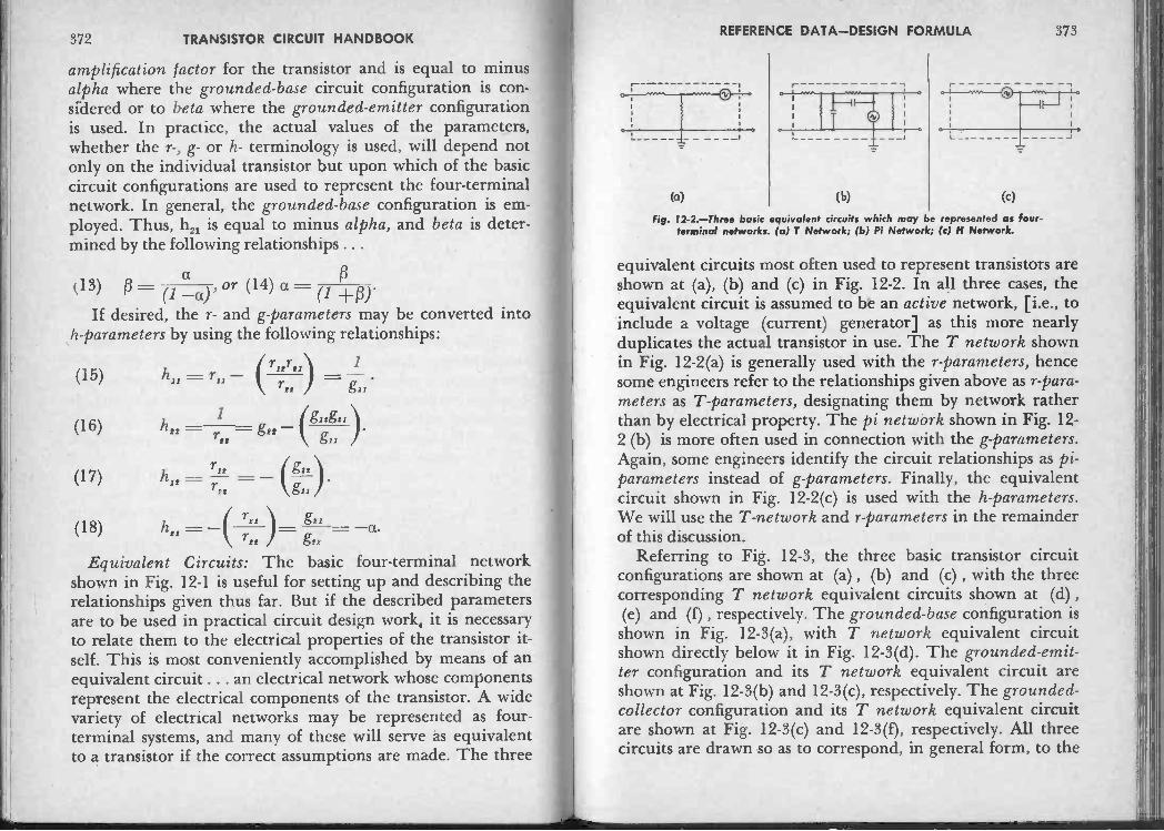
372 TRANSISTOR CIRCUIT HANDBOOK REFERENCE DATA-DESIGN FORMULA 373
amplification factor for the transistor and is equal to minusalpha where the grounded -base circuit configuration is con-sidered or to beta where the grounded -emitter configurationis used. In practice, the actual values of the parameters,whether the r-, g- or h- terminology is used, will depend notonly on the individual transistor but upon which of the basiccircuit configurations are used to represent the four -terminalnetwork. In general, the grounded -base configuration is em-ployed. Thus, h21 is equal to minus alpha, and beta is deter-mined by the following relationships . . .
13) =-(1 _a , or (14) a -
(1 +13 ivIf desired, the r- and g -parameters may be converted into
h -parameters by using the following relationships:
(15) h r - rrr 1
gii
(16) ger(gitg21)g
a.ru g2s
Equivalent Circuits: The basic four -terminal networkshown in Fig. 12-1 is useful for setting up and describing therelationships given thus far. But if the described parametersare to be used in practical circuit design work, it is necessaryto relate them to the electrical properties of the transistor it-self. This is most conveniently accomplished by means of anequivalent circuit . . . an electrical network whose componentsrepresent the electrical components of the transistor. A widevariety of electrical networks may be represented as four -terminal systems, and many of these will serve as equivalentto a transistor if the correct assumptions are made. The three
h- 1 - -r
(0) (b) (c)
Fig. 12-2.-Three basic equivalent circuits which may be represented as four -terminal networks. (a) T Network; (b) Pi Network; (c) H Network.
equivalent circuits most often used to represent transistors areshown at (a), (b) and (c) in Fig. 12-2. In all three cases, theequivalent circuit is assumed to be an active network, [i.e., toinclude a voltage (current) generator] as this more nearlyduplicates the actual transistor in use. The T network shownin Fig. 12-2(a) is generally used with the r -parameters, hencesome engineers refer to the relationships given above as r -para-meters as T -parameters, designating them by network ratherthan by electrical property. The pi network shown in Fig. 12-2 (b) is more often used in connection with the g -parameters.Again, some engineers identify the circuit relationships as pi -parameters instead of g -parameters. Finally, the equivalentcircuit shown in Fig. 12-2(c) is used with the h -parameters.We will use the T -network and r -parameters in the remainderof this discussion.
Referring to Fig. 12-3, the three basic transistor circuitconfigurations are shown at (a) , (b) and (c) , with the threecorresponding T network equivalent circuits shown at (d) ,(e) and (f) , respectively. The grounded -base configuration isshown in Fig. 12-3(a), with T network equivalent circuitshown directly below it in Fig. 12-3(d). The grounded -emit-ter configuration and its T network equivalent circuit areshown at Fig. 12-3(b) and 12-3(c), respectively. The grounded -collector configuration and its T network equivalent circuitare shown at Fig. 12-3(c) and 12-3(f), respectively. All threecircuits are drawn so as to correspond, in general form, to the

374 TRANSISTOR CIRCUIT HANDBOOK REFERENCE DATA-DESIGN FORMULA 375
Fig. 12-3.-The three fundamental transistor circuit configurations together with their Tnetwork equivalent circuits. The grounded -base configuration is shown at (a) and (d); thegrounded -emitter configuration is shown at (b) and (e); the grounded -collector configuration
is shown at (c) and (f).
four -terminal network given in Fig. 12-1. The componentsmaking up the T network equivalent circuits are identified asfollows:
re-emitter resistance.rb-base resistance.re-collector resistance.retie-internal generator (voltage source) , withrm-mutual resistance for the network, andie-emitter current (through re) .
Referring back to Fig. 12-1 and to the r -parameter defini-tions (1) to (4), the T network equivalent circuit componentsare related to the r -parameters as follows:
I. In the grounded -base circuit, Figs. 12-3(a) and 12-3(d):(19) r11 = re + rb.(20) r22 - re +(21) r12 = rb(22) r21 = rb.
II. In the grounded -emitter circuit, Figs. 12-3(b) and 12-3 (e) :
(23) r11 = rb re.(24) r2, = re + re - rm.(25) r1, = re.(26) r21=-- re - rm.
III. In the grounded -collector circuit, Figs. 15-3 (c) and15-3 (f) :
(27) r11= re(28) r22 = re + re - rin(29) r12 = re - rm.(30) r2, = re.
Approximate Amplifier Design Formula: Typical oper-ating transistor T network equivalent circuits are given inFig. 12-4. These are similar to the circuits given in Fig. 12-3,but with the addition of a load resistance (RL) and a signalvoltage source (E.) having an internal resistance (RG) . Im-pedances (Z) may be substituted for resistances if desired.D.C. supply sources are omitted for reasons of clarity. If a fewsimple, but legitimate, assumptions are made, it is possible todescribe each of the three circuits in terms of relatively simpledesign formulas. These formulas are given below and holdtrue for most circuit design work involving standard junctiontransistors. For more exact design equations, and for the deri-vation of the formulas given below, the reader should referto the very excellent references listed in the Bibliography
Fig. 12-4.-The three fundamental transistor circuit configurations shown as their operatingT network equivalent circuits. The emitter, base, and collector connections are identifiedoutside the dotted box, which represents the transistor proper. The grounded -base con-figuration is shown at (a), the grounded -emitter configuration at (6), and the grounded -
collector configuration at (c).
376 TRANSISTOR CIRCUIT HANDBOOK
(Chapter 14). In the following formulas it is assumed thatthe sum of the emitter resistance (re) and the base resistance(rb) is much less than the load resistance (R,) and that thisvalue, in turn, is much less than the network's mutual re-sistance (rm) ; it is also assumed that the sum of the emitterand base resistances (re + rb) is much less than the signalsource's internal impedance (RG) and that this value, in turn,is much less than the collector resistance (re) :
I. In the grounded -base circuit, Fig. 15-4 (a) :
(31)(32)
(33)
(34) Current Amplification a.
a 2RL
aRL
Input Impedance - r, ± rb(1 -a).Output Impedance re.
Voltage Amplification re + rb(1 -a)
(35) Power Gain -__-_ re + rb(1 -a)II. In the grounded -emitter circuit, Fig. 15-4 (b) :
re(36)
(37)
(38)
(39)
(40)
Input Impedance rb -a.Output Impedance re(1 - a).
aRLVoltage Amplification re +
-rb(1 -a)*
Current Amplificationa2RLPower Gain
re(1 -a) ± rb(1 -a)2*III. In the grounded -collector circuit, Fig. 15-4 (c) :
(41) Input Impedance - ((3 + 1)R1.(42) Output Impedance 11G(1 -a).(43) Voltage Amplification 1.
(44) Current Amplification + 1.(45) Power Gain - 1.
In all of the above formulas, the current amplification fac-tors, alpha (a) and beta ((3) are as defined earlier. See SECTION Aof this chapter.
PART IV-REFERENCE DATA
Chapter 13
SPECIAL TECHNIQUES - NEW DEVELOPMENTS
SECTION A: Special TechniquesPrinted Circuits: Transistors and printed circuit techniques
are related from an historical viewpoint. Both becameimportant parts of the American Industrial Scene at aboutthe same time. But there are other relationships - themajority of currently available transistorized equipment hasbeen manufactured using printed circuits; transistors, be-cause of their small physical size, long life, and low powerrequirements, are ideal components for the assembly of sub-miniature equipment . . . and printed circuit techniques areideal as manufacturing methods for such equipment. Becauseof these close relationships, as well as the growing importanceof printed circuit techniques, the author felt it would be ger-mane to discuss printed circuits as a part of this volume. How-ever, he hastens to point out that printed circuits are notconfined to transistor circuitry, nor must all transistor equip-ment be assembled using printed circuit techniques. Printedcircuits are applicable to all types of wiring, even includingnon -electronic electrical applications. And transistors may beused in circuits wired using older "conventional" techniques.
Basically, printed circuits are electrical circuits in whichindividual wire lead connections have been replaced by atwo-dimensional conductive pattern bonded to an insulatingbase material. The name itself is derived from one of thescore or more techniques that are used for producing suchcircuits. Although there are many different techniques thatmay be used to manufacture printed circuits, most of thesemay be classed as belonging to one of two major systems.Where deposit methods are used, the conductive pattern is
377
378 TRANSISTOR CIRCUIT HANDBOOK SPECIAL TECHNIQUES -NEW DEVELOPMENTS 379
deposited directly upon the insulating base material. Wherestripping techniques are used, the insulating base is coveredwith the conductive material (usually metallic, such as cop-per, brass, aluminum or silver) ; the final circuit is made byremoving excess material to leave the desired pattern. Eitherchemical etching or electrical or mechanical methods maybe used to strip away the unwanted conductor.
Among the deposit methods are printing, painting, spray-ing, plating and hot -die stamping. Two or more of thesemethods may be combined; for example, a thin conductivepattern may be printed on an insulating base, then later builtup with metallic layers deposited by an electroplating process.Conducting (metallic) , insulating and resistive inks or paintsmay be used with the first three methods, permitting com-ponents (resistors and capacitors) as well as conducting leadsto be formed. A metallic foil is generally used with the hot -die stamping process, with the foil imbedded slightly in thebase material by the die. Where hot -die stamping is used, thebase may be paper, plastic, laminated phenolic, rubber, orsimilar materials. All of these materials may be used withthe printing, painting, and spraying methods, as well as glassand various ceramics. If a glass or ceramic base is used, theprinted circuit may be fused in place by high -temperaturefiring, assuring an extremely strong and stable bond. If theconductive material is applied by painting, a brush or penmay be used "freehand" for individual jobs, or a stencil orsilk screen pattern employed for production runs. A stencilor mask is employed when the conductive material is to besprayed onto the insulating base. Deposit techniques arewidely used in the production of small components (resistorsand capacitors) and compact network and single stage as-semblies, although, at this writing, these techniques are notused extensively in the production of complete equipmentcircuits.
The more popular stripping methods include stamping,embossing, and etching. In most cases, where stripping tech-
niques are employed, the raw material is a metal -clad lami-nate. Copper -clad phenolics are used extensively. Both thestamping and embossing methods use dies. With the stampingtechnique, the metallic foil is cut out by a die having theshape of the desired circuit. After stamping, the unwantedfoil is stripped away from the base, leaving the finished cir-cuit. Where the embossing method is used, the metallic foilis pressed into the surface of the insulating base material bythe pressure of a die having the proper shape for the desiredcircuit. After pressing, the embossed surface is cut away, usingeither a milling device or abrasive action. This operationremoves all the exposed metallic surfaces except those pressedinto the insulating material and beyond the reach of the cut-ting device. The finished circuit pattern is actually embeddedin the base material. Where the etching technique is em-ployed, a special resist material is deposited on the metallicfoil in the pattern of the desired circuit. The metal -clad lami-nate is then exposed to the etching ("eating away") actionof a chemical solution which attacks all the exposed foil butis held back by the resist wherever it covers the metal. Afterall the excess foil is etched away, the resist is removed andthe final etched circuit is ready for further processing. Allthree stripping techniques have been used in the manufactureof printed circuits, but etching is by far the most popularand is worthy of more detailed discussion. Stripping tech-niques are used most often in the preparation of completeequipment circuits, but have been used in the preparationof components, principally inductance coils, small capacitors,and switch assemblies.
As mentioned above, the etching method is currently themost popular process for producing printed circuits. A ma-jority of manufacturers use this technique, with copper -cladlaminate (usually phenolic base) serving as the basic ma-terial and ferric chloride solution serving as an etchant. Ac-tual manufacturing techniques vary widely, however, princi-pally in the type of "resist" used, in the way the resist is
380 TRANSISTOR CIRCUIT HANDBOOK
applied, and in the way the etchant is applied. The principalmethods now used are outlined briefly below:
Ink and Paint Resists-An acid resistant ink or paint isapplied to the metallic surface of the laminate in the patternof the desired circuit. For small "custom" jobs, the paintmay be applied with a brush or pen. For short productionruns, a silk-screen or similar stencil may be employed.
Photoengraving-The copper -clad laminate is coated witha light-sensitive enamel. The prepared laminate is then ex-posed to strong light through a negative of the circuit draw-ing and the enamel developed to obtain an acid resist pattern.The unexposed material is removed during the developingprocess, leaving a protective covering only where light struckthe surface of the laminate.
Offset printing-The circuit pattern is printed on the cop-per -clad laminate using a plate prepared, photographically,from an original circuit drawing. While the ink is still wet,asphalt powder is dusted onto the ink and fused at a moder-ately high temperature to form an acid resistive pattern.
Plated resists-A reverse of the circuit pattern is printedon the copper -clad phenolic. The laminate is then electro-plated with a metal that is unaffected by the ferric chlorideused to etch the copper (silver, solder, hard nickel or rhodi-um may be used) . The plating is deposited only where thecircuit pattern appears for the reverse ink pattern preventsthe plating from taking place on other areas. After plating,the ink is removed using an appropriate solvent, leaving ex-posed copper except where the plated pattern covers thesurface.
Etching-After the copper -clad laminate has been coveredwith a resist in the desired circuit pattern, the board is etchedin a ferric chloride or similar acid solution. The unprotectedcopper is eaten away, leaving a conductive pattern onlywhere the copper is protected by the resist. Several etchingtechniques are employed. Still etching is the slowest andconsists simply of immersing the laminate in a tray or tank
SPECIAL TECHNIQUES -NEW DEVELOPMENTS 381
of the etchant solution. A somewhat more rapid method isto use a deep tank of etchant, agitated with air bubblessupplied from a compressor. Air -agitated baths are suitablefor mass production. Even more rapid etching may be ac-complished by using a splash etching process. A machine isused in which small paddles splash the etchant against theprepared copper -clad laminate boards. The most rapid andmost efficient etching method is that employing a sprayprocess. Small nozzles direct the etchant solution against thelaminate boards in a steady spray.
When the etching is completed, the boards are washed andcleaned. Ink or photographic resists are removed with ap-propriate solvents or by mechanical abrasion. Mounting holesare drilled or punched in the circuit boards, small componentsare mounted by passing their leads through the holes, and thecompleted circuit finished by soldering all connections simul-taneously by dipping the board in a tank of molten solder.
The methods just described are especially well suited tothe mass production of electronic circuits, and it is in quantityproduction that printed circuit techniques find their greatestapplication at the present time. To the manufacturer, the useof printed circuits offers a great reduction in labor costs over"hand -wiring," which may represent as much as 50% of theproduction costs of "conventionally -wired" electronic equip-ment. In addition, when compared to hand -wired circuits,printed circuits are less costly from a materials viewpoint,more compact, faster to assemble, and consistently alike, as-suring better quality control and more consistent operationof the final product. Finally, since wiring errors are elimi-nated, final inspection processes are simplified and less costly.
Printed circuits may offer the advantages of simplified cir-cuit layout, compact construction, and better circuit perform-ance to the laboratory worker as well as to the manufacturer.Recognizing this fact, several manufacturers have made upbasic "kits" containing the materials necessary to the produc-tion of printed circuits and have offered these kits to labora-

382 TRANSISTOR CIRCUIT HANDBOOK SPECIAL TECHNIQUES -NEW DEVELOPMENTS 383
tory workers, home experimenters, and prototype equipmentdesigners. Two such kits are shown in Figs. 13-1 and 13-2.
Any one of several different methods may be used by thelaboratory worker in making up a "one-shot" etched circuit.The chief difference in the various methods is in the typeof resist used. The three most popular methods are illustratedin Fig. 13-3. Shown are a tape resist, an ink resist, and anegative such as might be used with the photographic process.Regardless of the type of resist used, essentially the same step-by-step process is followed in making up a complete printedcircuit assembly. The important steps are as follows:
(1) Initial circuit layout to scale.(2) Preparation of the copper -clad laminate board.
Fig. 13-1.-A KEPRO Etched Circuit Kit. The kit includes copper laminate, ink resist, etchingsolution, steel wool, an etching tray, a small brush, and full instructions.
(3) Transfer of the layout to the board as a pattern of resist.(4) Etching the laminate.(5) Removing the resist.(6) Machining the board.(7) Final assembly.
Let us discuss each of these steps in turn.(1) Initial layout: Before work on the circuit board itselfcan be started, a scale layout of the desired circuit must beprepared. The layout shows the location of all componentsand the position of all conductors on the final board. If tapeor ink resists are to be used, the layout may be full-sized. Ifa photographic process is to be used, it is customary to makethe initial layout four times full size, then to reduce to full
Fig. 13-2.-A TECHNIQUES Printed Circuit Kit. Designed for small laboratories, this kitincludes copper laminate, tube sockets, ink resist, tape resist, a small drill, eyelets, and
packes of etching powder, together with full instructions.

384 TRANSISTOR CIRCUIT HANDBOOK
Fig. 13-3.-Three popular techniques used for making up "one-shot" etched circuits in thelaboratory. Reading from left to righ, the methods shown include tape resist, ink resist,
and a photographic negative far a printed circui layout.
size photographically. Such reduction of the initial layoutminimizes errors and insures a finer finished job.(2) Board preparation: Once the layout is completed, theoverall dimensions of the final board can be determined anda piece of copper -clad laminate cut to size. A fine hacksaw,scroll saw, or jigsaw may be used for this operation. Oncecut to size, the copper foil surface is carefully cleaned andwashed to remove dirt and grease, then scrubbed with pumiceor an abrasive household cleanser to develop a slightlyroughened surface. Etching is much faster if the surface ofthe copper is roughened slightly. If a photographic processis to be used, the light sensitive solution is flowed evenlyacross the surface of the board and allowed to dry.
SPECIAL TECHNIQUES -NEW DEVELOPMENTS 385
(3) Transferring the layout: If tape or ink resists are to beused, the full-scale layout is transferred to the surface of thecopper foil in any manner desired by the individual worker.Many workers prefer to trace the layout pattern on the cop-per foil, using the layout drawing and stencil carbon. Othersprefer to transfer the layout drawing using dividers and simi-lar means. Regardless of the method used, once the patternis on the board, the paths of conductors are covered with theresist, whether Scotch tape or acid resistant ink. The tapeis simply pressed into place and burnished flat with a smoothtool. The ink may be flowed on using a pen or fine brush.If several identical boards are to be prepared, a paper orsilk screen stencil of the layout may be prepared and the inkapplied through the stencil. If a photographic process is to
Fig. 13-4.-After the desired layout has been ransferred to the copper -clad laminateas a pattern of resist, the board is etched in an enamel or plastic tray.

386 TRANSISTOR CIRCUIT HANDBOOK SPECIAL TECHNIQUES -NEW DEVELOPMENTS 387
be used, the prepared board is simply exposed to a strong lightthrough the previously prepared full-size negative. A strongwhite or ultra -violet light is generally used. The exposuretime varies with the light, but is generally on the order ofseveral minutes. Once exposed, the board is developed. Theexact development technique will depend on the chemicalsused . . . follow the manufacturers' recommendations here.(4) Etching: With the pattern of resist on the board, awarm solution of ferric chloride is placed in an enamel, plas-tic, or glass tray, and the board placed in the tray so that itis completely covered by the etchant. See Fig. 13-4. The solu-tion is agitated during the etching process. The board maybe removed from time to time for inspection. Don't allowthe etchant to touch bare skin . . . use rubber gloves andtongs. When all excess copper has been etched away, washthe board in clear water. Remove all traces of etchant.(5) Removing the resist: With the etching completed andthe board washed, the resist must be removed. Tape resist issimply stripped off. Ink or photographic resist is removedby scrubbing with fine steel wool.(6) Machining: Small holes are drilled through the boardwhere leads are to pass through and where components areto be mounted. Special care must be taken not to crack theboard. In general, it is best to drill from the copper foil side.(7) Final assembly: Small brass or copper eyelets may bemounted in holes where connections are likely to be removedoften. Parts are mounted simply by passing their leads throughappropriate holes. Large components, such as tuning capaci-tors, may be held in place by small machine screws, nuts,and brackets. "One-shot" circuits are usually hand -soldered(as opposed to the dip -soldering technique employed in mass
production). Use a small tip (11/2") hot soldering iron anda low melting point solder (such as G -C No. 9131) . Com-plete the soldering as quickly as possible. Too much heat willresult in the copper foil separating from the insulating base.Although components may be mounted on both sides of an
etched circuit board, it is customary to mount all the com-ponents on the side opposite that of the conductors. A typicaletched circuit board, seen from the "wiring" side, is shownin Fig. 13-5.
Fig. 13-5.-A ypical etched circuit board.
Potting: Another technique often used with, but not con-fined to, transistor circuits, is that of "potting" a completedcircuit. Potting is simply encapsulating a circuit or compo-nent in a plastic -like material that completely surrounds itand serves to enclose and protect it. The basic idea of pottingis not new. Transformers, capacitors, electrical networks, andsimilar components have been potted since the early days ofradio. Pitch and various hard waxes were used in the pastbut, more recently, various resins have been employed. Pot-
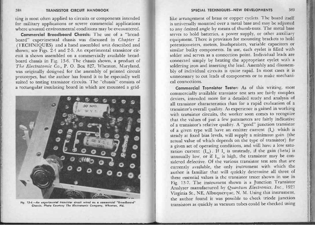
388 TRANSISTOR CIRCUIT HANDBOOK SPECIAL TECHNIQUES -NEW DEVELOPMENTS 389
ting is most often applied to circuits or components intendedfor military applications or severe commercial applicationswhere unusual environmental conditions may be encountered.
Commercial Breadboard Chassis: The use of a "bread-board" experimental chassis was discussed in Chapter 2(TECHNIQUES) and a hand assembled unit described andshown; see Figs. 2-4 and 2-5. An experimental transistor cir-cuit is shown assembled on a commercially available bread-board chassis in Fig. 13-6. The chassis shown, a product ofThe Electratomic Co., P. 0. Box 827, Wheaton, Maryland,was originally designed for the assembly of printed circuitprototypes, but the author has found it to be especially wellsuited to testing transistor circuits. The "chassis" consists ofa rectangular insulating board in which are mounted a grid -
Fig. 13-6.-An experimental transistor circuit wired on a commercial "Breadboard"Chassis. Photo Courtesy The Electratomic Company, Wheaton, Md.
like arrangement of brass or copper eyelets. The board itselfis universally mounted over a metal base and may be adjustedto any desired angle by means of thumb -nuts. The metal baseserves to hold batteries, a power supply, or other auxiliaryequipment. There is provision for mounting brackets to holdpotentiometers, meters, loudspeakers, variable capacitors orsimilar bulky components. In use, each eyelet is filled withsolder and serves as a connection point. Individual leads areconnected simply by heating the appropriate eyelet with asoldering iron and inserting the lead. Assembly and disassem-bly of individual circuits is quite rapid. In most cases it isunnecessary to cut leads of components or to make mechani-cal connections.
Commercial Transistor Tester: As of this writing, mostcommercially available transistor test sets are fairly complexdevices, intended more for a detailed study and analysis ofall transistor characteristics than for a rapid evaluation of atransistor's overall quality. As experience is gained in workingwith transistor circuits, the worker soon comes to recognizethat the values of just a few parameters are fairly indicativeof a transistor's relative quality. A "good" junction transistorof a given type will have an emitter current (Ie) which issteady at fixed bias levels, will supply a minimum gain (theactual value of which depends on the type of transistor) fora given set of operating conditions, and will have a low satu-ration current (Ico) . If Ie is unsteady, if the gain (beta) isunusually low, or if lco is high, the transistor may be con-sidered defective. Of the various transistor test sets that arecurrently available, the only instrument with which theauthor is familiar that will quickly determine all three ofthese essential values is the transistor tester shown in use inFig. 13-7. The instrument shown is a Junction TransistorAnalyzer manufactured by Quantum Electronics, Inc., 1921
Virginia St., NE, Albuquerque, N. M. Using this instrument,the author found it was possible to check triode junctiontransistors as quickly as vacuum tubes could be checked using

390 TRANSISTOR CIRCUIT HANDBOOKSPECIAL TECHNIQUES -NEW DEVELOPMENTS 391
Fig. 13-7.-Using a QUANTUM Junction Transistor Analyzer to check transistors.
a "service" type emission tube tester. The Quantum transistortester is, itself, transistorized and completely self-contained,with its own built-in power supply. It includes a built-inoscillator supplying an A.C. signal for checking beta as wellas appropriate switches and controls for establishing Ie andfor checking Ico. It handles both NPN and PNP junctiontransistors. Self -calibration is provided to compensate for longterm drift and unusual ambient temperature conditions.
In operation, only five switches or controls are adjusted.One switch is set for the type of transistor being tested (NPNor PNP), another for the measurement desired (Ie, beta, orIco) , and another for the beta range to be used. Betas of 0-50or 0-100 may be measured. One control is used for initialcalibration for any given set of tests and another is used toset I. to a fixed level for beta measurements.
SECTION B: New Developments
The Melt -Back Process: A new method of transistormanufacture developed by General Electric in which wire -
shaped crystals rather than sliced semiconductor ingots areused. Because of the small size of the crystals, the meltedsemiconductor material cools rapidly and there is less inter-mixing or contamination between adjacent semiconductorlayers. The process may be used to produce semiconductorcrystals in which the layer of impurities is as thin as 1/5000".The transistors produced by this process have extremely highgains and are usable at frequencies much higher than tran-sistors produced using older processes. As of this writing,transistors made by the new process are not available on thecommercial market.
Zone Metter: A device developed by the Bureau of Stand-ards to obtain high -purity semiconductor materials. In opera-tion, the solid material to be purified is placed in a fusedslicia or carbon boat within a glass tube. A water-cooled in-duction coil, coaxial with the tube, is passed slowly along thelength of the tube. The semiconductor is rapidly heated tomelting point by eddy currents induced by the R.F. energyflowing through the inductance coil. This melting takesplace only iii a narrow zone, however, which is within thedirect influence of the coil. As the coil moves along, themolten zone moves along with it. Impurities tend to separateat the zone boundaries, so after the material has been melteda number of times, impurities tend to concentrate at oneend of the bar . . . which may then be cut off.
Diflusion Techniques: Relatively new methods used in themanufacture of high frequency, low to medium power tran-sistors. Three procedures for manufacturing transistors bydiffusion are in current use. The diffused -base and double -
diffusion techniques were developed by Bell Telephone Lab-oratories, the grown -diffused method by Texas Instruments.All three techniques are based on the solid-state diffusion of
impurity atoms through semiconductor material under pre-

392 TRANSISTOR CIRCUIT HANDBOOK
cisely controlled conditions involving the accurate control oftemperature, chemical purities, and other factors.
In the diffused -base method, small bars of one type of semi-conductor material are cut, lapped, polished, and given aslight etch. These bars eventually serve as the collector layer.Where PNP transistors are to be made, the bars might be cutfrom P-type germanium. After washing, the bars are placedin an oven where a small amount of impurity is diffused ontothe surface to form a thin base layer. Again, to make a PNPtransistor, arsenic -doped germanium could be used as a sourceof N -type impurity. Next, a thin film of metal (aluminum inthe example) is evaporated onto a small masked area, thenalloyed to the bar with heat, forming the emitter area. As afinal step, the bar may be masked again and additional metallicdeposits made for electrode connections. Diffused -base tech-niques have been used to make germanium transistors withan alpha -cutoff frequency of 400-600 Mc and a collector dissi-pation of 150 milliwatts.
Double -diffused transistors may be made in any of severalways, but one common technique relies on differences in thediffusion rates of various semiconductor impurities. In prac-tice, selected donor and acceptor impurities may be diffusedsimultaneously into a prepared bar of, say, N -type semicon-ductor, which eventually serves as the collector. One impuritydiffuses faster into the semiconductor, getting ahead of theother, and forming a base layer of opposite characteristics. Forexample, a N -type semiconductor bar may be used, togetherwith a fast -diffusing acceptor and a slow -diffusing donor im-purities. The acceptor impurity, diffusing faster than thedonor, gets ahead of it and forms an intermediate P -type layerbetween the inner and outer N -type layers, resulting in a NPNtransistor. After diffusion, the semiconductor bar is completelycovered with diffused N-type and P -type layers, with the cen-tral bar forming the collector, the intermediate layer the base,and the outer layer the emitter. Final base contact is made byalloying directly through the outer emitter area. Connectionto the central collector is made by masking the unit and etch -
SPECIAL TECHNIQUES -NEW DEVELOPMENTS 393
ing away the unwanted layers in a limited area. The double -diffusion technique has been used to make silicon transistorswith alpha -cutoff frequencies of 100-120 Mc and collectordissipations of 500 milliwatts.
The grown -diffused method developed by Texas Instru-ments utilizes solid-state diffusion techniques while the crystalis being grown, resulting in an ultra -thin base region. Silicontransistors produced with this technique give good gains upto 30Mc, or more, while maintaining useful power outputs totemperatures of 150°C. Germanium units have been producedwith cutoff frequencies of 200 Mc, and collector dissipationratings of 25 milliwatts at 75°C.
Prior to the application of diffusion techniques to the pro-duction of transistors, similar methods were used to producehigh power semiconductor rectifiers with extremely high effi-ciencies. As an example, two pea -sized units mounted on acooling fin are able to furnish better than 20 amperes at 100volts, with only 20 watts lost in heat dissipation. It would ap-pear that similar techniques might one day result in truly"high -power" transistors.
Special Purpose Transistors: A number of specialized tran-sistors and related semiconductor devices have been designedand manufactured, both in the laboratory and in pilot plantquantities. These units are different from the usual "specialtransistors", such as junction tetrodes, R.F. units, low -noiseadio transistors, sub -miniature units, and "hi -power" transis-tors, both in construction and in application. Among the typesthat have been made are the Field -Effect transistor, the Tan-dem transistor, the "Thyratron" transistor, and the Double -based diode. It is expected that other special units will bedeveloped by manufacturers and offered in the future.
The Field -Effect transistor is a unipolar semiconductor de-vice which differs from junction transistors in that currentflow is predominantly by one type of carrier (electrons or"holes") and that this current flow is caused by field driftrather than slow diffusion, a relatively high electric field in-tensity (voltage) being employed between electrodes. This

394 TRANSISTOR CIRCUIT HANDBOOKSPECIAL TECHNIQUES -NEW DEVELOPMENTS 395
unit features a high input and high output impedance, andhas moderately good frequency response. Pilot plant unitshave been used as oscillators up to 10 or 12 Mc.
The Tandem transistor is essentially two junction triodetransistors in a single housing, with a direct internal connec-tion between the emitter of one transistor and the base of thesecond unit. It is roughly analogous to a "multi -purpose"vacuum tube which consists of two separate tubes in a singleenvelope. In operation, the unit acts like a grounded -collectoramplifier stage direct -coupled to a grounded -emitter stage.The first unit serves as the "base leak" of the second stage. Itis used as a self-contained cascade amplifier and features highinput as well as good output impedances. In addition, varyingthe input base bias current varies the gain considerably, per-mitting the unit to be used as a variable gain device . . . rough-ly similar to a variable mu vacuum tube. MARVELCO in-troduced these units.
The "Thyratron" transistor, developed by IBM, and pro-duced in experimental quantities, is a unique unit with ajunction emitter and point -contact collector. It has the "allor nothing" characteristic which is analogous to a thyratronthermionic tube and, for this reason, is named after the earlierdevice. In operation, in the grounded -emitter configuration,a small base current will keep the collector load current low.If the base current is removed, however, the emitter -collectorimpedance drops and a high load current can flow . . . the tran-sistor is "on". To turn the unit "off", the base current mustbe returned and the collector voltage dropped to a low value.Since the semiconductor material used (germanium) is sensi-tive to light, the unit can also be switched with a light signal.
The Double -based diode provides an action very similar tothat of a "thyratron" transistor, in that it may be used as aswitching device with an "off" and an "on" state. The basicunit consists of a rectifying junction made to a bar, the endsof which are terminated in ohmic connections. It is called adouble -based diode because it is similar in construction to anordinary crystal diode having two bases and, in fact, if the two
connections are tied together electrically, the unit will oper-ate as a conventional diode. The double -based diode is thussimilar to a junction tetrode transistor, but without the collec-tor electrode and connection. Under some operating condi-tions the double -based diode exhibits a negative -resistanceinput characteristic, permitting its use in astable, monostable,and bistable multivibrators, as well as in counters, oscillators,and phase detectors, in addition to its basic switch operation.Pilot production of double -based diodes has been started byGeneral Electric but, as of this writing, test samples were notavailable for circuit investigation.
The author hopes to include circuits for many of these spe-cial purpose semiconductor devices in future additions of theTRANSISTOR CIRCUIT HANDBOOK . . . as well as cir-cuits for other, as yet undeveloped, units. Among the possiblefuture devices could be a "complementary -symmetry" tandemtransistor . . . essentially a cascaded NPN-PNP transistor pairin a single hermetically sealed container, with the collector ofone direct -coupled, internally, to the base of the second unit.Still another possibility would be a push-pull complementary -symmetry tandem transistor . . . again, a NPN-PNP pair, butwith matched characteristics and with the collector electrodesdirect -coupled internally . . . a type of self-contained single -ended push-pull amplifier.
396 TRANSISTOR CIRCUIT HANDBOOK
Credit: Bell Telephone Laboratories
Apparatus used at Bell Telephone Laboratories to control, automatically, diffusion processused in making new high frequency transisors. Panel at left controls flow of chemicalimpurities and gas through the tubes coiled in tank of water in center. From tubes, im-purities are introduced into oven at the right, where, under gas and at carefully regulatedtemperatures, hey are diffused ino material. An attendant can easily check the progressof the diffusion process.
PART IV-REFERENCE DATA
Chapter 14
BIBLIOGRAPHY
Published transistor literature is running a course similarto that followed by literature in any new technical field.Starting as a small trickle, it has progressed to a veritable floodand now covers the gamut of literary effort . . . from popularaccounts to the most profound technical papers. A completeand comprehensive listing of all transistor literature would re-quire more space than can be allotted to the subject in thisvolume. Therefore, the author has had to exercise consider-able discretion in choosing items to be listed. The selectionof any article, book or paper over some other does not implyit is in any way superior to an unlisted work. In many cases,the author's guiding rule has been availability. Unfortunately,some of the most valuable published works have had a limiteddistribution. For the convenience of the reader, the author hassubdivided the Bibliography into types of publications, withseparate listings of books, trade publications, magazine articles,and similar topics. The section on Magazine Articles andTechnical Papers has been further subdivided into subjectcoverage. In each section, the works are listed in numericalorder. This listing is sometimes arbitrary and sometimeschronological. In no case is the listing order intended to indi-cate the relative importance of the individual works.
BIBLIOGRAPHIC LISTS
1. TRANSISTOR REPORT CATALOG: Office of TechnicalServices, U .S. Department of Commerce, Washington 25, D. C.(10c).
2. TRANSISTOR BIBLIOGRAPHY (Magazine Artides FeaturingRaytheon Transistors) : Raytheon Manufacturing Co., 55 ChapelStreet, Newton 58, Massachusetts.
397

398 TRANSISTOR CIRCUIT HANDBOOK BIBLIOGRAPHY -SPECIAL ARTICLES 399
3. GUIDE TO TRANSISTOR LITERATURE, 1954: The GlennL. Martin Company, Presentations Section, Engineering Division,Baltimore 3, Maryland.
4. TRANSISTORS AND THEIR APPLICATIONS -A BIBLI-OGRAPHY, 1948-1953, Alan R. Krull: Technological InstituteLibrary, Northwestern University Library, Evanston, Illinois.
5. TRANSISTOR RESEARCH BULLETIN, Volume 1, Nos. 1 to6: National Scientific Laboratories, Inc., 2010 MassachusettsAvenue, N. W., Washington 6, D. C.
BOOKS AND BOOKLETS1. APPLICATIONS OF TRANSISTORS TO ELECTRONIC
COUNTING EQUIPMENT, Richard E. Kimes: Office of Tech-nical Services, Department of Commerce, Washington 25, D. C.(Publication No. PB 111610-$2.00) .
2. THE TRANSISTOR: SELECTED REFERENCE MATERIALON CHARACTERISTICS AND APPLICATIONS, Bell Tele-phone Laboratories, Inc.: Available from Office of TechnicalServices, U. S. Department of Commerce, Washington 25, D. C.(Publication No. PB 111054-$20.00) .
3. TRANSISTOR APPLICATIONS (50 Practical Circuits usingRaytheon CK722 Transistors) : Raytheon Manufacturing Co.,55 Chapel Street, Newton 58, Massachusetts (50c) .
4. 28 USES FOR JUNCTION TRANSISTORS: Sylvania ElectricProducts, Inc., 1740 Broadway, New York 19, N. Y. (25c) .
5. POWER REQUIREMENTS FOR TRANSISTOR CIRCUITS,J. Dalfonso: P. R. Mallory & Co., Inc., North Tarrytown, N. Y.
6. THE SURFACE -BARRIER TRANSISTOR, Members of theTechnical Staff, Philco Research Division: Philco Corporation,4700 Wissahickon Ave., Philadelphia 44, Pa. (Reprints of aseries of articles appearing originally in Proc. of the I.R.E.) .
7. APPLICATION NOTES ON THE PHILCO SURFACE BAR-RIER TRANSISTOR: Philco Corporation, 4700 WissahickonAve., Philadelphia 44, Pa.
8. SURFACE BARRIER TRANSISTOR SWITCHING CIR-CUITS: Philco Corporation, 4700 Wissahickon Ave., Philadelphia44, Pa.
9. TRANSISTORS, Louis E. Garner, Jr. (Coyne, Distributed byHoward W. Sams) .
10. TRANSISTORS -THEORY AND PRACTICE, Rufus P. Turner(Gernsback) .
11. FUNDAMENTALS OF TRANSISTORS, Leonard Krugman(Rider) .
12. TRANSISTORS -THEORY AND APPLICATIONS, A. Cob-lenz and H. Owens (McGraw-Hill) .
13. ELECTRONS AND HOLES IN SEMICONDUCTORS, WilliamShockley (Van Nostrand) .
14. PRINCIPLES OF TRANSISTOR CIRCUITS, R. F. Shea et al(Wiley) .
15. TRANSISTOR AUDIO AMPLIFIERS, R. F. Shea (Wiley) .
The booklets listed below are published by the Technical Publica-tions Group of the BELL TELEPHONE SYSTEM and are, for themost part, reprints of technical papers and articles by staff membersof the Bell Telephone Laboratories, which were originally publishedin such journals as THE PHYSICAL REVIEW, ELECTRICALENGINEERING, the BELL SYSTEM TECHNICAL JOURNAL,ELECTRONICS, and PROCEEDINGS OF THE I.R.E.16. THE TRANSISTOR AND RELATED EXPERIMENTS, Bar-
deen, Brattain, Shockley, and Pearson: Monograph B-1574 (origi-nal paper, June, 1948) .
17. TRANSISTORS, Becker, Shive, Kock, Wallace: MonographB-1640.
18. SOME CONTRIBUTIONS TO TRANSISTOR ELECTRON-ICS: Monograph 1726.
19. DUALITY AS A GUIDE IN TRANSISTOR CIRCUIT DE-SIGN, Wallace. Raisbeck: Monograph 1874.
20. PROPERTIES OF p -n JUNCTION TRANSISTORS, Shockley,Sparks, Teal, Wallace, and Pietenpol: Monograph 1909 (originalpaper, July, 1951) .
21. TRANSISTOR CIRCUIT DESIGN, Raisbeck: Monograph 1932.22. PRESENT STATUS OF TRANSISTOR DEVELOPMENT,
Morton: Monograph 1993.23. TRANSISTOR EQUATIONS, Stansel: Monograph 2066.24. A JUNCTION TRANSISTOR TETRODE FOR HIGH -
FREQUENCY USE, Wallace, Schimpf,, Dick ten: Monograph 2089.25. FOUR -TERMINAL p -n -p -n TRANSISTORS, Ebers: Monograph
2099.26. TRANSISTOR ELECTRONICS: IMPERFECTIONS, UNI-
POLAR, AND ANALOG TRANSISTORS, Shockley: Mono-graph 2101.
TRADE PUBLICATIONS
A number of manufacturers publish periodicals which are sent toqualified people in the field on request, sometimes gratis and some-times for a nominal subscription fee. To the author's knowledge,there is no such publication devoted exclusively to transistors; how-
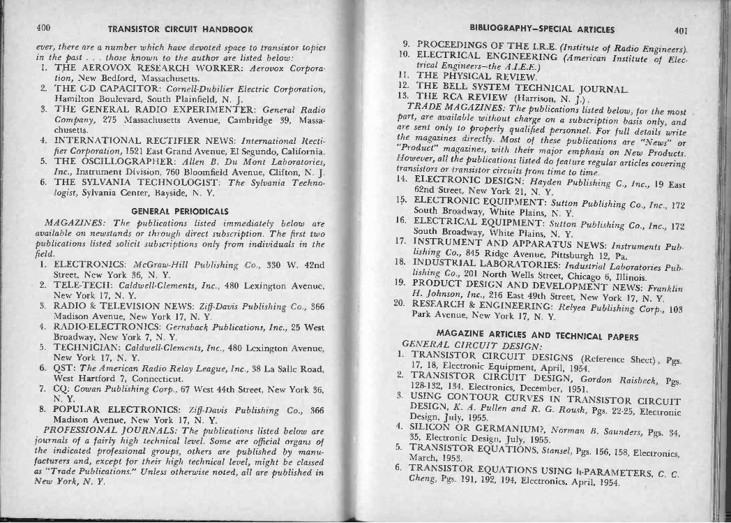
400 TRANSISTOR CIRCUIT HANDBOOK
ever, there are a number which have devoted space to transistor topicsin the past . . . those known to the author are listed below:1. THE AEROVOX RESEARCH WORKER: Aerovox Corpora-
tion, New Bedford, Massachusetts.2. THE C -D CAPACITOR: Cornell-Dubilier Electric Corporation,
Hamilton Boulevard, South Plainfield, N. J.3. THE GENERAL RADIO EXPERIMENTER: General Radio
Company, 275 Massachusetts Avenue, Cambridge 39, Massa-chusetts.
4. INTERNATIONAL RECTIFIER NEWS: International Recti-fier Corporation, 1521 East Grand Avenue, El Segundo, California.
5. THE OSCILLOGRAPHER: Allen B. Du Mont Laboratories,Inc., Instrument Division, 760 Bloomfield Avenue, Clifton, N. J.
6. THE SYLVANIA TECHNOLOGIST: The Sylvania Techno-logist, Sylvania Center, Bayside, N. Y.
GENERAL PERIODICALSMAGAZINES: The publications listed immediately below are
available on newstands or through direct subscription. The first twopublications listed solicit subscriptions only from individuals in thefield.
1. ELECTRONICS: McGraw-Hill Publishing Co., 330 W. 42ndStreet, New York 36, N. Y.
2. TELE-TECH: Caldwell -Clements, Inc., 480 Lexington Avenue,New York 17, N. Y.
3. RADIO & TELEVISION NEWS: Ziff -Davis Publishing Co., 366Madison Avenue, New York 17, N. Y.
4. RADIO -ELECTRONICS: Gernsback Publications, Inc., 25 WestBroadway, New York 7, N. Y.
5. TECHNICIAN: Caldwell -Clements, Inc., 480 Lexington Avenue,New York 17, N. Y.
6. QST: The American Radio Relay League, Inc., 38 La Salle Road,West Hartford 7, Connecticut.
7. CQ: Cowan Publishing Corp., 67 West 44th Street, New York 36,N. Y.
8. POPULAR ELECTRONICS: Ziff -Davis Publishing Co., 366Madison Avenue, New York 17, N. Y.
PROFESSIONAL JOURNALS: The publications listed below arejournals of a fairly high technical level. Some are official organs ofthe indicated professional groups, others are published by manu-facturers and, except for their high technical level, might be classedas "Trade Publications." Unless otherwise noted, all are published inNew York, N. Y.
BIBLIOGRAPHY-SPECIAL ARTICLES 401
9. PROCEEDINGS OF THE I.R.E. (Institute of Radio Engineers).10. ELECTRICAL ENGINEERING (American Institute of Elec-trical Engineers-the A.I.E.E.)
11. THE PHYSICAL REVIEW.12. THE BELL SYSTEM TECHNICAL JOURNAL.13. THE RCA REVIEW (Harrison, N. J.).
TRADE MAGAZINES: The publications listed below, for the mostpart, are available without charge on a subscription basis only, andare sent only to properly qualified personnel. For full details writethe magazines directly. Most of these publications are "News" or"Product" magazines, with their major emphasis on New Products.However, all the publications listed do feature regular articles coveringtransistors or transistor circuits from time to time.14. ELECTRONIC DESIGN: Hayden Publishing C., Inc., 19 East
62nd Street, New York 21, N. Y.15. ELECTRONIC EQUIPMENT: Sutton Publishing Co., Inc., 172
South Broadway, White Plains, N. Y.16. ELECTRICAL EQUIPMENT: Sutton Publishing Co., Inc., 172
South Broadway, White Plains, N. Y.17. INSTRUMENT AND APPARATUS NEWS: Instruments Pub-
lishing Co., 845 Ridge Avenue, Pittsburgh 12, Pa.18. INDUSTRIAL LABORATORIES: Industrial Laboratories Pub-lishing Co., 201 North Wells Street, Chicago 6, Illinois.19. PRODUCT DESIGN AND DEVELOPMENT NEWS: FranklinH. Johnson, Inc., 216 East 49th Street, New York 17, N. Y.20. RESEARCH & ENGINEERING: Relyea Publishing Corp., 103Park Avenue, New York 17, N. Y.
MAGAZINE ARTICLES AND TECHNICAL PAPERSGENERAL CIRCUIT DESIGN:
1. TRANSISTOR CIRCUIT DESIGNS (Reference Sheet) , Pgs.17, 18, Electronic Equipment, April, 1954.2. TRANSISTOR CIRCUIT DESIGN, Gordon Raisbeck, Pgs.128-132, 134, Electronics, December, 1951.3. USING CONTOUR CURVES IN TRANSISTOR CIRCUITDESIGN, K. A. Pullen and R. G. Roush, Pgs. 22-25, Electronic
Design, July, 1955.4. SILICON OR GERMANIUM?, Norman B. Saunders, Pgs. 34,35, Electronic Design, July, 1955.5. TRANSISTOR EQUATIONS, Stansel, Pgs. 156, 158, Electronics,March, 1953.6. TRANSISTOR EQUATIONS USING h -PARAMETERS, C. C.
Cheng, Pgs. 191, 192, 194, Electronics, April, 1954.

402 TRANSISTOR CIRCUIT HANDBOOK BIBLIOGRAPHY-SPECIAL ARTICLES 403
7. DESIGNING RELIABLE TRANSISTOR CIRCUITS-I, N. B.Saunders, Pgs. 24-27, Electronic Design, March, 1955.
8. DESIGNING RELIABLE TRANSISTOR CIRCUITS-II, N.B. Saunders, Pgs. 37-39, Electronic Design, April, 1955.
9. TRANSISTOR CIRCUIT COMPONENTS, Wright Air De-velopment Center (available from the Library of Congress, Pub-lication Board Project, Washington 25, D. C.) .
10. OPERATING TRANSISTORS AT HIGHER VOLTAGES, G.H. Didinger, Pgs. 44, 45, Electronic Design, July, 1955.
11. JUNCTION TRANSISTOR CIRCUIT APPLICATIONS, P.G. Sulzer, Pgs. 170-173, Electronics, August, 1953.
12. JUNCTION TRANSISTOR PULSE FORMING CIRCUITS,J. B. Oakes, Pgs. 165-167, Electronics, September, 1954.
13. JUNCTION TRANSISTOR SWITCHING CIRCUITS, T. A.Prugh, Pgs. 168-171, Electronics, January, 1955.
14. TRANSISTORS USE EMITTER -COUPLED FEEDBACK, F. C.Alexander, Jr., Pgs. 188, 190, 192, Electronics, December, 1954.
15. DIRECTLY COUPLED TRANSISTOR CIRCUITS, R. H.Beter, W. E. Bradley, R. B. Brown, M. Rubinoff, Pgs. 132-136,Electronics, June, 1955.
16. TRANSISTORS GENERATE MULTIWAVEFORMS, E. Keon-jian and J. J. Suran, Pgs. 138, 139, Electronics, July, 1955.
17. TRANSISTOR C -R TUBE DEFLECTION CIRCUITS, J. W.Taylor, Jr. and T. M. Moore, Pgs. 146-149, Electronics, July, 1955.
18. SURFACE -BARRIER TRANSISTOR MEASUREMENTS ANDAPPLICATIONS, R. J. Turner, Tele-Tech, August, 1954.
19. PHOTODIODES AND PHOTOTRANSISTORS-I, R. G. Seedand R. B. Holt, Pgs. 8, 9, Electronic Design, September, 1953.
20. PHOTODIODES AND PHOTOTRANSISTORS-II, R. G. Seedand R. B. Holt, Pgs. 10, 11, Electronic Design, November, 1953.
21. FIELD EFFECT TRANSISTOR CIRCUIT DESIGN-I, C.Huang, W. Marshall and B. H. White, Pgs. 38, 39, ElectronicDesign, July, 1955.
AMPLIFIER DESIGN:22. TRANSISTORIZE YOUR AUDIO AMPLIFIERS, C. W. Martel,
Pgs. 40, 41, 125, 126, Radio 8c Television News, March, 1953.23. DIRECT -COUPLED TRANSISTOR AMPLIFIERS, R. B. Hur-
ley, Pgs. 26-28, Electronic Equipment, April, 1955.24. TRANSISTOR CHOPPERS FOR STABLE D -C AMPLIFIERS,
R. L. Bright and A. P. Kruper, Pgs. 135-137, Electronics, April,1955.
25. TRANSIENT ANALYSIS OF TRANSISTOR AMPLIFIERS,W. F. Chow and J. J. Suran, Pgs. 189-191, Electronics, November,1953.
26. NOISE IN TRANSISTOR AMPLIFIERS, E. Keonjian and J. S.Schaffner, Pgs. 104-107, Electronics, February, 1953.
27. GAIN -STABILIZED TRANSISTOR AMPLIFIER, C. A. Krause,Pgs. 183-185, Electronics, February, 1954.
28. TEMPERATURE -STABILIZED TRANSISTOR AMPLIFIERS,H. J. Tate, Pgs. 144-147, Electronics, June, 1954.
29. FEEDBACK -STABILIZED TRANSISTOR AMPLIFIER, D. W.Slaughter, Pgs. 174, 175, Electronics, May, 1955.
30. FEEDBACK IN JUNCTION TRANSISTOR CIRCUITS, D.W. Gade, Pgs. 174-176, 178, Electronics, June, 1954.
31. FEEDBACK SIMPLIFIES TRANSISTOR AMPLIFIERS, S.
Schenkerman, Pgs. 129-131, Electronics, November, 1954.32. PRACTICAL TWO -STAGE TRANSISTOR AMPLIFIERS, R.
L. Riddle, Pgs. 169-171, Electronics, April, 1954.33. TRANSISTOR AMPLIFIERS FOR ANALOG COMPUTERS,
G. M. Ettinger, Pgs. 119-121, Electronics, July, 1955.POWER AMPLIFIER DESIGN:
34. DESIGN OF TRANSISTOR POWER AMPLIFIERS, S. K.Ghandhi, Pgs. 146-149, Electronics, March, 1954.
35. POWER TRANSISTOR CIRCUIT DESIGN, Pgs. 14-15, Elec-tronic Equipment, August, 1954.
36. DESIGN PROCEDURES FOR POWER TRANSISTORS-I,H. T. Moore, Pgs. 58-61, Electronic Design, July, 1955.
37. DESIGN PROCEDURES FOR POWER TRANSISTORS-II,H. T. Moore, Pgs. 42-45, EleCtronic Design, September, 1955.
38. CLASS B OPERATION OF TRANSISTORS-I, K. E. Loof-bourrow, Pgs. 28-31, Electronic Design, July, 1955.
39. CLASS B OPERATION OF TRANSISTORS-II, K. E. Loof-bourrow, Pgs. 34-37, Electronic Design, August, 1955.
40. RATING TRANSISTORS TO PREVENT "RUNAWAY," N.DeWolf, Pgs. 28-29, Electronic Design, February, 1955.
41. HIGH FIDELITY TRANSISTOR POWER AMPLIFIER, R. L.Riddle, Pgs. 174, 176, Electronics, September, 1955.
MAGNETIC AMPLIFIERS:42. TRANSISTOR -CONTROLLED MAGNETIC AMPLIFIER, R.
H. Spencer, Pgs. 136-140, Electronics, August, 1953.43. TRANSISTOR PREAMPLIFIER DRIVES MAGNETIC
SERVO, M. B. Zucchino, Pgs. 168-171, Electronics, March, 1954.COMPLEMENTARY SYMMETRY:

404 TRANSISTOR CIRCUIT HANDBOOKBIBLIOGRAPHY-SPECIAL ARTICLES 405
44. SYMMETRICAL PROPERTIES OF TRANSISTORS ANDTHEIR APPLICATIONS, G. C. Sziklai, Pg. 717, Proceedingsof the I.R.E., June, 1953.
45. COMPLEMENTARY SYMMETRY TRANSISTOR CIRCUITS,R. D. Lohman, Pgs. 140-143, Electronics, September, 1953.
46. COMPLEMENTARY SYMMETRY, R. H. Spencer (Letter) ,Pgs. 426, 428, Electronics, April, 1953.
HIGH FREQUENCY (R.F.) DESIGN:47. HIGH -FREQUENCY TRANSISTOR TETRODE, R. L. Wal-
lace, Jr., L. G. Schimpf, E. Dickten, Pgs. 112-113, Electronics,January, 1953.
48. HIGH -FREQUENCY TRANSISTOR AMPLIFIERS, W. F.Chow, Pgs. 142-145, Electronics, April, 1954.
49. HOW TO DESIGN I -F TRANSISTOR TRANSFORMERS,R. G. Webster, Pgs. 156-158, 160, Electronics, August, 1955.
50. HIGH FREQUENCY TRANSISTORS, Pgs. 32-33, ElectronicDesign, February, 1955.
51. VHF TRANSISTOR OSCILLATORS, H. E. Hollmann, Pgs.220, 222, 224, 226, Electronics, June, 1954.
52. JUNCTION TRANSISTORS FOR HIGH-FREQUENCY OS-CILLATORS, I. Queen, Pgs. 87-88, Radio -Electronics, August,1954.
53. DESIGN OF TRANSISTORIZED HIGH -GAIN PORTABLE,W. E. Sheehan and J. H. Ivers, Pgs. 159-161, Electronics, March,1955.
54. F -M TRANSISTOR OSCILLATOR, H. H. Wieder and N. Cass,Pgs. 198, 200, 202, Electronics, July, 1953.
55. TRANSISTOR CONVERTER, L. J. Hruska, Pgs. 212, 214, Elec-tronics, September, 1954.
TESTS AND MEASUREMENTS:56. METHODS AND EQUIPMENT FOR TRANSISTOR TEST-
ING, B. J. O'Neill and A. Gutterman, Pgs. 172-175, Electronics,July, 1953.
57. TEST TECHNIQUES FOR TRANSISTORS, R. P. Turner,Pgs. 78, 80, 82, Radio -Electronics, March, 1953.
58. JUNCTION TRANSISTOR CHECKER, E. Bohr, Pgs. 30-32,Radio -Electronics, August, 1954.
59. TESTER FOR TRANSISTOR SELECTION, N. H. Kramer,Pgs. 240, 242, 244, Electronics, June, 1954.
60. CATHODE-RAY TUBE PLOTS TRANSISTOR CURVES, J.Kurshaw, R. D. Lohman, G. B. Herzog, Pgs. 122-127, Electronics,February, 1953.
61. OBTAINING TRANSISTOR CHARACTERISTIC CURVES,W. Philbrook, Pgs. 66-67, Radio & Television News, September,1953.
62. VERSATILE TRANSISTOR TESTER, J. Gibbons, Pgs. 10-11,46, Radio Electronic Engineering section of Radio & TelevisionNews, June, 1954.
63. A BRIDGE FOR JUNCTION TRANSISTOR MEASURE-MENTS, D. Dorman, Pgs. 10-11, 39, Radio -Electronic Engineeringsection of Radio & Television News, October, 1954.
64. A SIMPLE TRANSISTOR TESTER, Pgs. 3-9, C -D Capacitor,May, 1954.
65. TRANSISTOR MEASUREMENTS WITH THE VACUUM -TUBE BRIDGE, A. G. Bousquet, Pgs. 1-4, General Radio Ex-perimenter, March, 1953.
66. TRANSISTOR AMPLIFIER-CUTOFF FREQUENCY, D. E.Thomas, Pgs. 1481-1482, Proceedings of the I.R.E., November,1952 (Reprinted as Bell Telephone System Technical PublicationsMonograph 2095).
67. MEASURING TRANSISTOR TEMPERATURE RISE, J. Tel-lerman, Pgs. 185-187, Electronics, April, 1954.
FOREIGN:68. BRITISH TRANSISTOR APPLICATIONS, D. D. Jones, Pgs.
54-57, Electronic Design, July, 1955.69. USSR SEMICONDUCTOR RADIO RECEIVER, Pgs. 20-21,
Electronic Design, August, 1955.70. USSR TRANSISTOR DATA CHART, Pgs. 162-162, Electronic
Design, September, 1955.71. USSR TRANSISTORIZED SUPERHET RECEIVER, Pg. 169,
Electronic Design, September, 1955.
MAGAZINE ARTICLES (APPLICATIONS)
GENERAL CIRCUIT INFORMATION:1. SPECIAL-PURPOSE TRANSISTOR CIRCUITS, Pgs. 3-10, C -D
Capacitor, February, 1955.2. JUNCTION TRANSISTOR CIRCUITS, The Aerovox Re-
search Worker, April -May, 1953.3. TRANSISTOR FLIP-FLOP USES TWO FREQUENCIES, R.
L. Brock, Pgs. 175-177, Electronics, June, 1954.4. TRANSISTOR PULSE SUPPLY, T. A. Prugh and J. W. Keller,
Pgs. 188, 190, 192, 194, 197, Electronics, July, 1954.

406 TRANSISTOR CIRCUIT HANDBOOK BIBLIOGRAPHY-SPECIAL ARTICLES 407
5. AGC FOR TRANSISTOR AMPLIFIERS, Pgs. 224, 226, 228,Electronics, January, 1954.
6. DEMONSTRATION TRANSISTOR CIRCUITS, E. Bohr, Pgs.45-47, Radio -Electronics, December, 1954.
7. TRANSISTOR AMPLIFIERS REDUCE DELAY LINE AT-TENUATION, A. H. Schooley, Pgs. 181-183, Electronics, May,1954.
8. SIMPLE CIRCUIT STABILIZES TRANSISTOR, F. E. Barron,Pgs. 182, 184, 186, Electronics, May, 1954.
AUDIO AMPLIFIERS:9. PUSH-PULL TRANSISTORS, Pgs. 68, 72, Radio -Electronics,
June, 1953.10. LOW -DRAIN HEARING AID, Pg. 36, Radio -Electronics, Sep-
tember, 1954.12. LOW -NOISE TRANSISTOR PREAMPLIFIER, R. P. Turner,
Pg. 64, Radio -Electronics, August, 1954.13. SELECTIVE A -F TRANSISTOR AMPLIFIER, D. Bier and
S. Rosen, Pgs. 208, 210, Electronics, December, 1954.14. A PRACTICAL TRANSISTOR PREAMP, B. Edelman, Pgs.
39, 86, Radio 8c Television News, August, 1955.15. TRANSISTOR GUITAR AMPLIFIER, L. E. Garner, Jr., Pgs.
74-75, 192-193, Radio & Television News, November, 1953.16. A TRANSISTORIZED APPLAUSE METER, L. E. Garner, Jr.,
Pgs. 82-83, 120-121, Radio Sc Television News, March, 1954.OSCILLATORS:
17. TRANSISTOR OVERTONE GENERATOR, I .Queen, Pg. 59,Radio -Electronics, December, 1954.
18. TRANSISTOR AM TEST OSCILLATOR, E. Bohr, Pgs. 52-54,Radio -Electronics, September, 1954.
19. LOW -DISTORTION TRANSISTOR AUDIO OSCILLATOR,P. G. Sulzer, Pgs. 171-173, Electronics, September, 1953.
20. TRANSISTOR PHONO OSCILLATOR, E. Bohr, Pgs. 74, 76,Radio -Electronics, May, 1954.
21. SELF -KEYED TRANSISTOR OSCILLATOR, P. C. Alexander,Jr., Pgs. 214, 216, Electronics, July, 1954.
22. STABILIZED TRANSISTOR AUDIO OSCILLATOR, Pg. 208,Electronics, December, 1953.
23. I.F.-R.F. CRYSTAL OSCILLATOR USES JUNCTION TRAN-SISTOR, I. Queen, Pgs. 92, 94, Radio -Electronics, May, 1954.
24. TRANSISTOR SAWTOOTH OSCILLATOR, H. G. Ruden-berg, Pgs. 50-51, Radio -Electronics, November, 1952.
25. TRANSISTOR OSCILLATOR CIRCUIT, L. Fleming, Pgs.196, 198, Electronics, June, 1953.
26. TRANSISTOR DIP OSCILLATOR, R. P. Turner, Pgs. 51, 85,Radio Sc Television News, July, 1955.
27. A TRANSISTOR CODE PRACTICE OSCILLATOR, L. E.Garner, Jr., Pgs. 40-41, 99, Radio Sc Television News, April, 1953.
28. A TRANSISTORIZED AUDIO OSCILLATOR, L. E. Garner,Jr., Pgs. 68-69, Radio & Television News, September, 1953.
29. A SUBMINIATURE CODE PRACTICE OSCILLATOR, L. E.Garner, Jr., Pgs. 40-41, Radio & Television News, February, 1954.
30. A PUSH-PULL TRANSISTOR AUDIO OSCILLATOR, L. E.Garner, Jr., Pgs. 48-50, Popular Electronics, April, 1955.
RECEIVERS:31. TRANSISTOR BROADCAST REGENERATOR, P .G. Sulzer,
Pg. 200, Electronics, June, 1953.32. REGENERATIVE TRANSISTOR RECEIVER, Dr. W. H.
Grace, Jr., Pgs. 84-85, Radio -Electronics, August, 1954.33. TRANSISTORIZED WRIST -RADIO, U. S. Department of
Commerce, Office of Technical Services, Washington 25, D. C.(No. PB 111461, 25c) .
34. BUILD THIS TRANSISTOR RECEIVER, R. K. Dixon, Pgs.35-37, 132, Radio 8c Television News, February, 1953.
35. POCKET RADIO, H. G. McEntee, Pgs. 205-207, 264, PopularScience Monthly, September, 1954.
36. TRANSISTOR PORTABLE GETS ALL THE STATIONS,H. G. McEntee, Pgs. 209-214, Popular Science Monthly, September,1955.
37. TRANSISTOR RADIO USES NO POWER SUPPLY, 1)r. W.H. Grace, Jr., Pg. 96, Radio -Electronics, April, 1955.
38. TRANSISTORIZED INTERFLEX RECEIVER, Dr. W. H.Grace, Jr., Pgs. 54-55, Radio -Electronics, August, 1955.
39. ALL TRANSISTOR AUTOMOBILE RECEIVER, Pg. 50, RadioSc Television News, July, 1955.
TRANSMITTERS AND HAM GEAR:40. SOLARIZED QSO, E. Laird Campbell, Pgs. 11, 110, CQ, Sep-
tember, 1955.
408 TRANSISTOR CIRCUIT HANDBOOK
41. A TRANSISTORIZED AUDIO FILTER FOR AMATEURRECEPTION, Raytheon Mfg. Co., 55 Chapel Street, Newton 58,Massachusetts.
42. TRANSISTOR FREQUENCY STANDARD, P. G. Sulzer, Pgs.206, 208, 210, 212, 214, Electronics, May, 1953.
43. A NEW, SENSITIZED GRID -DIP ADAPTOR, Pgs. 3-7, C -DCapacitor, August, 1955.
44. SENSITIVE TRANSISTORIZED FIELD STRENGTH ME-TER, Aerovox Research Worker, Part I, July, 1955; Part II,August, 1955.
TEST INSTRUMENTS:45. TRANSISTOR POWER SUPPLY FOR GEIGER COUNTERS,
A. R. Pearlman, Pgs. 144, 145, Electronics, August, 1954.46. VEST-POCKET TRANSISTOR ALPHA METER, B. P. Ker-
foot, Pgs. 216, 218, 220, 222, 224, Electronics, December, 1953.47. TRANSISTORIZED VOLTMETER, R. P. Turner, Pgs. 54-55,
Radio -Electronics, December, 1954.48. A TRANSISTOR OPERATED LIGHT METER, L. E. Garner,
Jr., Pgs. 93-96, Popular Electronics, March, 1955.49. TRANSISTORIZED SINE -WAVE GENERATOR, L. E. Garner.
Jr., Pgs. 43-45, Popular Electronics, September, 1955.50. A number of transistorized test instruments are described in
Raytheon's TRANSISTOR APPLICATIONS book . . . see itemNo. 3 under BOOKS AND BOOKLETS in this Bibliography.
PATENTS
The U. S. Patents listed below represent only a fraction of the totalnumber of patents issued covering transistors and transistor circuits.These were chosen because they have been referred to or reviewed intrade literature and, therefore, may be considered to be of more thancasual interest. In order to conserve space, only the last names of theinventors have been given. The titles listed may not be the "official"title in every case . . . liberties have been taken in a few instances toprovide a more descriptive listing. In most cases, the firms to whichthe patents are assigned are shown in parentheses in abbreviated form."RCA" refers to the Radio Corporation of America; "BTL" to theBell Telephone Laboratories, Inc. The "basic" transistor patent isgenerally considered to be U.S. Pat. No. 2,524,035 (BTL).
1. FILAMENT TYPE TRANSISTOR, No. 2,502,479, Pearson andShockley (BTL) .
BIBLIOGRAPHY -SPECIAL ARTICLES 409
2. N -P JUNCTION TRANSISTOR, No. 2,502,488, Shockley (BTL) .3. TRANSISTOR HAVING HIGH IMPEDANCE INPUT, No.
2,524,033, Bardeen (BTL) .4. FIELD CONTROLLED TRANSISTOR, No. 2,524,034, Brattain
and Gibney (BTL) .5. TRANSISTOR MICROPHONE, No. 2,549,550, Shockley (BTL) .6. JUNCTION TRANSISTOR, No. 2,569,347, Shockley (BTL) .7. MAKING SEMICONDUCTOR DEVICES, No. 2,629,672, Oliver
(BTL) .8. LINE CONTACT TRANSISTOR, No. 2,580,027, Johnson
(RCA) .9. SEMICONDUCTOR TRANSLATING DEVICE, No. 2,651,831,
Bond, Sparks, Teal (BTL) .10. TRANSISTOR AMPLIFIER CIRCUITS, No. 2,652,460, Wal-
lace (BTL) .11. ELECTRIC SEMICONDUCTOR, No. 2,653,374, Matthews and
White (International Standard Electric Company of New York) .12. MAKING SEMICONDUCTOR DEVICES, No. 2,654,059, Sparks
(BTL) .13. SEMICONDUCTOR SIGNAL TRANSLATING DEVICE, No.
2,655,610, Ebbers (BTL) .14. FOUR -ELECTRODE TRANSISTOR MODULATOR, No.
2,657,360, Wallace (BTL) .15. INVERTED GROUNDED EMITTER TRANSISTOR AMPLI-
FIER, No. 2,659,773, Barney (BTL) .16. BIDIRECTIONAL TRANSISTOR AMPLIFIER, No. 2,659,774,
Barney (BTL) .17. TWO-WAY TRANSISTOR ELECTRICAL TRANSMISSION
SYSTEM, No. 2,662,122, Ryder (BTL) .18. TRANSISTOR "FOLLOWER," No. 2,663,796, Raisbeck and
Wallace (BTL) .19. FREQUENCY CONTROLLED TRANSISTOR OSCILLATOR,
No. 2,663,800, Herzog (RCA) .20. SEMICONDUCTOR SIGNAL TRANSLATING DEVICES, No.
2,663,806, Shockley (BTL) .21. TRANSISTOR SIGNALING, No. 2,666,812, Kircher (BTL) .
22. TRANSDUCER, No. 2,666,861, Campbell (Reed Research, Inc.) .
23. REGENERATIVE TRANSISTOR AMPLIFIER, No. 2,670,445,Felker (BTL) .

410 TRANSISTOR CIRCUIT HANDBOOK INDEX24. SEMICONDUCTOR TRANSLATING DEVICE, No. 2,672,523,
Shockley (BTL) .25. TWO -TERMINAL SINE WAVE OSCILLATOR, No. 2,675,474,
Eberhard (RCA) .
26. TRANSISTOR BIAS CIRCUIT, No. 2,680,160, Yaeger (BTL) .27. TRANSISTOR OSCILLATOR, No. 2,681,996, Wallace (BTL) .28. SEMICONDUCTOR CURRENT CONTROL DEVICE, No.
2,689,930, Hall (General Electric Co.) .
29. TRANSISTOR SYSTEM FOR TRANSLATING SIGNALS INTWO DIRECTIONS, No. 2,691,073, Lowman (Hazeltine Re-search, Inc.) .
30. TRANSISTOR AMPLIFIER FOR LOW DISTORTION, No.2,691,077, Koros (RCA) .
31. OSCILLATION GENERATOR, No. 2,692,337, Hanson (BTL) .32. PUSH-PULL SINE -WAVE OSCILLATOR, No. 2,698,386, Eber-
hard and Endres (RCA) .
33. SEMICONDUCTOR FREQUENCY CONVERTER, No. 2,701,-302, Giacoletto (RCA) .
34. SEMICONDUCTOR OSCILLATION GENERATOR, No.2,701,309, Barney (BTL) .
35. TRANSISTOR MODULATION SYSTEM, No. 2,702,316, Friend(RCA) .
36. VARIABLE PROFILE TRANSISTORS, No. 2,702,361, Seilerand Fedotowski (International Standard Electric Corporation) .
37. PN JUNCTION TRANSISTOR, No. 2,705,767, Hall (GeneralElectric Co.) .
38. COAXIAL TRANSISTORS, No. 2,707,310, Conrad (Stromberg-Carison Co.) .
39. TRANSISTOR MULTIVIBRATOR, No. 2,707,752, Gabler(North American Aviation, Inc.)
40. TRANSISTOR TRIGGER CIRCUIT, No. 2,708,720, Anderson(BTL) .
41. CONSTANT VOLTAGE SEMICONDUCTOR DEVICE, No.2,709,780, Kircher (BTL) .
42. HETERODYNE CONVERTER, No. 2,713,117, Haegele (Syl-vania Electric Products, Inc.
43. SELF -POWERED SEMICONDUCTOR DEVICES, No. 2,713,644,Rappaport (RCA) .
AAbsorption Frequency Meter, 205Acceleration due to Gravity (g), 25, 359Acceptor, 3, 353, 361, 365, 392Accordian, electronic, 317A.G. Power Supplies, 44A.G. Relay, 329Admittance, 364A.F., 354AFC, 353 ,A.F. Coils, 39-40A.F. Transformers, 39-40AGC, 353Alarm, Burglar, 290Alarm, Rain, 286-290Alignment, 188, 227, 363Alpha, 8, 112-114, 353, 372, 376Alpha cut-off frequency, 67, 83-84, 113,
167Alpha measurement, 112-113Aluminum, 3Aluminum electrolytic, 35, 36Ambient temperature, 55Amplification factor, current (see alpha,
beta), 8, 112-114, 353, 372, 376Amplifier, 49-73, 353Amplifier, audio, 52-66Amplifier, buffer, 220, 224, 242Amplifier characteristics, 1Amplifier, class, 53-54, 64, 68, 354Amplifier, complementary, 258 (also see
Complementary amplifier andComplementary Symmetry)
Amplifier configurations, 11-13, 54Amplifier, D.C., 253, 257, 262, 263Amplifier, Direct -coupled, 49-52, 287,
288Amplifier, grounded -base, 1, 12-13, 30,
54Amplifier, grounded -collector, 1, 12-13,
30, 54Amplifier, grounded -emitter, 1, 11-13,
30, 54-56Amplifier, Headphone, 122-124Amplifier, Hearing Aid, 126-130Amplifier, magnetic, 73Amplifier, meter, 253-257Amplifier, phonogaph, 162-166Amplifier, power, 65, 124-126Amplifier, Public Address, 153-158Amplifier, push-pull, 124-126Amplifier, R.F., 68-71Amplifier, selective, 72, 134-137Amplifier, tetrode, 105Amplifier, video, 66-67Amplifying device, 279Amplitude stabilization, 79AM Tuner, Hi Fi, 179-183
Analog transistor, 10, 367Analogy, transistor to vacuum tube,
11-14, 50, 66Analysis, dynamic, 49Analysis, static, 49Annunciator, 290Antenna, Dummy, 227Antimony, 3Applause Meter, 269Arrangement of semiconductors, 10-11Arsenic, 3Attenuate, 359Audio, 354Audio amplifiers, 52-66Audio amplifier, selective, 72, 134-137Audiophiles, 179Audio Level Meter, 263, 269-272Audio Light Meter, 306-309Audio Mixer, 151-153Audio Noise Meter, 269Audio Output Meter, 269Audio Photometer, 306-309Audio Oscillators, 76-82Automatic assembly, 42Automatic Frequency Control (AFC),
353Automatic Gain Control (AGC), 353Automatic Volume Control (AVC), 70,
71, 95, 185, 227, 354AVC (see Automatic Volume Control,
above)
BBack resistance, 320Banjo, electronic, 313-314, 317Base, 4, 6, 10, 11, 13, 354, 418Base resistance, 167Basic circuits, 47-118Battery boxes, 43Battery life, 45-46Battery, mercury, 44-46Battery power supplies, 44Battery, Solar (see Battery, Sun)Battery, Sun, 46, 262, 264-265, 306-307,
330-333Battery Tester, 20Battery, zinc -carbon, 44-46Beats, 202Beat frequency oscillator (see B.F.O.)Beat, zero, 209bel, 356Beta, 249, 254, 256, 354, 372, 376Beta cut-off frequency, 83, 167Beta measurement, 113-114B.F.O., 198, 202, 214, 227-228, 301Bias, 13, 44, 54-56, 254, 355Bias, reverse, 307Bias, multivibrators, 100-101

Emitter-follower-(Cont.)(also grounded -collector)
Engineering, production, 31, 120Enviromental tests, 20-21Equipment, laboratory, 16
test, 20, 345Equivalent circuits, 372-375Etchant, 379, 381, 386Etched circuits, 378-387Etching, 8Excitation, shock, 239, 240Exposure meter, 268, 331
FFactor, current amplification, 8,
112-114, 353, 372, 376noise, 363stability, 366
Family of curves, 118Feedback, 60, 61, 70, 75-76, 302-303, 358
characteristic, 108degenerative, 60, 61, 66, 358, 363inverse, 60, 61, 66, 358, 363losses, 82negative, 60, 61, 66, 358, 363overall, 61positive, 60, 62, 72, 75, 79, 358-359,
363regenerative, 75, 358-359, 363R.F., 70-71tickler, 77, 84oscillator, tickler, 106, 213
Field effect, 359Field effect transistor, 67, 82, 368-369,
393Fieldistor, 359Figure of merit, 83Filter networks, 44
L -C, 321R -C, 321, 325
First detector, 356, 362Flip-flop, 93, 99-102Fly -wheel action, 97Formula, design, 375-376Forward characteristics, 107Forward current, 359Four -terminal network, 369-370Frequency, 359
alpha cut-off, 67, 83, 84, 113, 167beta cut-off, 83, 167boost, 62characteristics, high, 67compensation, 66-67cut-off, 83, 356drift, 224
Frequency doubler, 209-212Frequency meter, R.F., 205-209Frequency quadruplet, 212Frequency response, low, 67Frequency response measurement, 108Frequency response, 233, 239, 247
Frequency stability, 225Frequency tripler, 212Front end, 356Full-waire rectifier, 319-321
Gg, 25, 359Gain, 54, 249, 359
controls, 58-59measurement, 108power, 1, 376-377R.F., 71voltage, 1, 109, 376-377
Gallium, 3, 8Gate, 99-101, 368GB, 360GC, 360GE, 360Geigamp, 137-141Geiger counter, 321Generator, characteristic curve, 116
Pulse, 240-244R.F. Alignment, 222-228Sine Wave, 218-222Square -Wave, 233-240
Germanium, 2, 3, 7, 318Gimmic, 85Golden Ear, 180g -parameters, 363-364, 369-372Gravity, acceleration due to (g), 25, 359Grid, 4Ground, 12-13, 360Ground bus, 360Ground potential, 360Grounded -base, 1, 12-13, 30, 54, 360,
372, 373, 376Grounded -base oscillator, 81, 85-87Grounded -cathode, 12, 49, 360Grounded -collector, 1, 12-13, 30, 54,
360, 373, 376Grounded -emitter, I, 11-13, 30, 54-56,
360, 372-373, 376Grounded -grid, 12, 360Grounded -plate, 12, 360Grown -diffused, 393Guitar, electronic, 313, 317
HHalf -wave rectifier, 319-321Hall effect, 360Hall voltage, 360Ham Shack, 205Ham Station Monitor, 202-205Hardware, 42-44Harmonics, 97, 224, 230, 231, 233, 240Harmonic distortion, 125Hartley oscillator, 78-79, 84, 90, 105,
106HI FI AM Tuner, 179-183HI FI Preamplifier, 158-162High frequency characteristics, 67
High frequency oscillator, 212-215High frequency transistors, 67, 84, 87,
98, 167-168, 211Hiss, microphone, 148, 155Hiss, transistor, 122Holes, 2, 353, 360, 365Headphone Amplifier, 122-124Hearing Aid, 126-130Heat, 25Heat dissipation, 65Heat powered, 46Heat radiator, 28, 65Heat sink, 19, 27-28, 44, 65, 360h -parameters, 363-364, 369-372H Network, 373Hook transistor, PN, 368Humidity compensation, 32, 120Hybrid parameters, 364, 370-372
IIco, 249, 256, 265, 267I.F., 356, 361, 362I.F. amplifier, 70-71, 356, 361, 362Impedance, 361
circuit configurations, 110coupling, 57input, 1, 35, 53, 59, 109-110, 376-377load, 12matching, 52-54, 68, 76measurements, 109-110output, 1, 53, 109-110, 376-377power transistor, 66, 110
Impurity, 3, 353, 358, 361, 392(see donor and acceptor)
Indium, 3, 8Indium sulphate, 8Injection, Signal, 228-231, 233, 272Input characteristic, 107Interchangeability, 55, 60, 66, 70, 90Intercom, 141-146Interelectrode capacities, 167Intermediate frequency, 356, 361, 362Interstage coupling, 53, 57Intrinsic semiconductor, 365, 367, 368Inverse feedback, 60, 61, 66, 358, 363Inverters, phase, 62-64Isolation transformer, 278
JJeweler's pliers, 16Jeweler's screwdrivers, 16Jeweler's screwdrivers, using, 17-18Joints, lap, 19Junction, 361Junction and point -contact transistors,
comparison, 8Junction temperature, 55Junction transistor, 4, 6, 367Junction transistor, diffused, 6, 7Junction transistor, grown, 6, 7
KKiller, TV commercials, 297
LLaboratory equipment, 16Laminate, 379-387Lap joints, 19L -C filter networks, 321L -C oscillator, 315Lead sulfide, 2Leakage currents, 111, 249-252, 254, 256,
258, 265, 285, 288, 365Lens, 308Level Meter, Audio, 263, 269-272Life, battery, 45-46
shelf, 46transistor, 217
Light, 330beam receiver, 306-309beam throw, 296beam transmitter, 308Controlled Relay, 322Meters, 262-269Meter, Audio, 306-309modulated, 309
Light -powered, 46Limiter, 93-97Linear, 94Linotetrar, 42Load, 361Loading, circuit, 225Load impedance, 12Local oscillator, 212, 227Long -wave receiver, 215Losser circuits, 59Losses, 358Loudspeaker, 366Low frequency response, 67
MMagazine articles, 401-408Magnetic amplifier, 73Manufacturers, components, 350-352Manufacturers, test equipment, 346Manufacturers, transistors, 339Matched pair, 157, 163, 252Matching, 362Matching impedances, 52-54, 68, 76Maximum ratings, 26
absolute, 353Measurement, alpha, 112-113
beta, 113-114dynamic, 112-114frequency response, 108gain, 108impedance, 109-110static, 112-114
Measuring parameters, 44Megaphone, Power, 146-150Meltback process, 82, 391
Melter, zone, 391Mercury battery, 44-46Merit, Figure of, 83Meters, 26Meter amplifiers, 253-257Meter, applause, 269Meter applications, 330Meter, Audio Level, 263, 269-272
Audio Light, 306-309Audio Noise, 269Audio Output, 269Exposure, 268, 331Light, 262-269output, 221
Meter protection diodes, 330Meter, R.F. Frequency, 205-209Metronome, 309-313Microphone, 366
hiss, 148, 155wireless, 190-194
Migration, 2Mixer, 93, 97-99, 356, 362
Audio, 151-153tetrode, 105
Modifications, circuit, 31, 48Modulate, 318, 362Modulated light, 309Modulated R.F., 231, 277, 327-328Modulation, 104, 107Modulator, 362 (see detector)
bridge, 327-328Moisture Detector, 286-290Molecule, 2Monitor, Ham Station, 202-205Monitoring meter, 269Monostable circuit, 99-101
complementary, 180Mounting, power transistor, 65-66Multipliers, voltage, 319-321Multi -purpose transistors, 10Multivibrators, 88-90, 307Multivibrator, bias, 100-101
collector -coupled, 89-90complementary, 89-90, 231, 234direct -coupled, 88-90emitter -coupled, 88-89one-shot, 99-101
Musical toys, 313-317
NN -base, 6, 11, 368Negative feedback, 60-61, 66, 358, 363Network, filter, 44
four -terminal, 369-370H-, 373L -C filter, 321Pi-, 373R -C, 281-282, 315, 321, 325T-, 373
Neutralization, 68, 70-71, 358, 363Noise factor, 363
Noise level, 122Non-linear, 94, 97, 318, 362NPIN transistor, 367NPN, 10-11, 32, 67, 82NPN transistor, 367N -type semiconductor, 2, 7-8, 358, 361,
365, 388Nulling, 134
0One shot multivibrator, 99-101Operating characteristics, typical, 30-31Organ, electronic, 313-314, 317Oscillation, 62, 72, 80, 359
transient, 239Oscillator, 75-91, 363
audio, 76-82blocking, 90-91, 311, 315Clapp, 85-87Code Practice, 301-306Colpitts, 78-79, 84, 219, 303crystal controlled, 85-86, 90-91Hartley, 78-79, 84, 90, 105, 106high frequency, 212-215L -C, 315local, 212, 227phase -shift, 81push-pull, 303R -C, 79-80, 88-90relaxation, 326R.F., 82-87sawtooth, 88Surface Barrier transistor, 212TBTC, 84tetrode, 105-106tickler feedback, 98, 106, 213TPTG, 85two -stage, 79-81Wien Bridge, 79-80Zener, 324-326
Oscilloscope, 222, 234, 235, 239, 247,271, 326
display, 115-118Output characteristics, 107, 116Output impedances, 1, 53, 109-110,
376-377Overall feedback, 61Overload, 25, 233
PPadder, 227Pair, matched, 157, 163. 252Parameter, 338-339, 363, 369-372
g-, 363-364, 369-372hybrid, 364, 370-372measuring, 44r-, 363-364, 369-372
Patents, 408-410P -base, 6, 11, 368Peaks, transient, 288 _Peaking coils, 67
Peaking coils-(Cont.)series, 67shunt, 67
Pendulum, 309Periodicals, 400-401Phase, 1, 13, 54, 62, 358-359Phase -inverter, 62-64Phase -shift, 57, 66, 239, 247
oscillator, 81Phonograph amplifier, 162-166Phosphorus, 3Photocells, 262, 291, 330-333
Cadmium Sulfide, 262, 267, 321, 323relays, 290-297, 321-323selenium, 262, 267, 291, 306-307,
330-333self -generating (see photocell,
selenium and Sun Battery)Photoconductive cell, 264, 322Photodiode, 364Photoengraving, 380Photography, 280Photometer, Audio, 306-309Phototransistors, 10, 102-104, 364Phototransistor circuit, complementary,
103Pi network, 373Pi parameters, 373Piano, electronic, 317Piezoelectric, 42, 75, 80, 85-86Pin connections, 23-24Pip, 239Plate, 4Pliers, Jeweler's, 16PNP, 10-11, 32, 67, 82PN "Hook" transistor, 10PNP transistor, 367PNIP transistor, 367PNPN transistor, 10, 368Pocket Receiver, 174-179Point -contact transistor, 4, 8-11, 167,
368Point -contact and junction transistors,
comparison, 8Polarities, 10, 16, 26, 32, 48, 49Polarized relay, 329Police Receiver, 313Potential, Ground, 360Positive feedback, 60, 62, 72, 75, 79,
358-359, 363Potting, 387-388Power, 364Power amplifiers, 65, 124-126Power amplifier distortion, 66Power amplifier, push-pull, 124-126Power, audio circuits, 39
dissipation, 28gain, 1, 376megaphone, 146-150required by transistors, 45-46supplies, 44-46, 54
Power audio circuits-(Cont.)supplies, constant current, 20, 29, 44,,
112-115, 355transistors, 1, 27-29, 65-66transistor mounting, 65-66
Practice, rules of, 25-27Preamplifier, Hi Fi, 158-162Printed circuit, 39, 42, 377-387Probe, Signal Tracing, 272-278, 324-325P -type semiconductor, 2, 78, 353, 361,
365, 368Public Address Amplifier, 153-158Pulse, 231, 236, 238, 240-244, 246
circuits, 89-91Pulse generator, 240-244Push-pull circuits, 64Push-pull oscillator, 80-81, 303Push-pull power amplifier, 124-126
Q, 37-39, 68Quadrupler, frequency, 212Quadrupler, voltage, 319-321
RRadiator, heat, 28, 65Radio, Wrist, 313Rain Alarm, 286-290Range, 296, 308Ratings, Maximum, 26
Absolute Maximum, 353Ratio, Signal/Noise, 160R -C network, 281, 282, 315, 321, 325R -C oscillators, 79-80, 88-90R -C time constant, 101, 242, 312Receiver, Communications, 196, 198,
209, 214, 224, 227-228, 301crystal, 328Light Beam, 306-309Long -Wave, 215Police, 313Pocket, 174-179Regenerative, 170-174Short -Wave, 215, 227Simple, 168-170
Recording Level Indicator, 269Rectangular wave, 233-236Rectifier, 269, 318-321, 364
full -wave, 319-321half -wave, 319-321
Reflectivity, 262, 268Regenerative feedback, 75, 358-359, 363Regenerative Receiver, 170-174Relaxation oscillator, 326Relay, A.G., 329
circuits, 329Electric Eye, 290-297light controlled, 290-297, 322photocell, 290-297, 321-323polarized, 329Voice -Controlled, 297-301

Reliability, 217Remote control, 290, 292, 330Resist, 379-387Resistance, back, 320
base, 167Resistors, 34-35Resonant circuits, 67-72, 75, 97Response, frequency, 233, 239, 247Response, low frequency, 67Response measurement, frequency, 108Response, transient, 240Reverse bias, 307Reverse current, 325, 364, 369R.F., 364
Alignment Generator, 222-228amplifiers, 68-71applications, 167-215, 327-329coils, 37-39circuit coupling, 69circuit gain, 71feedback, 70-71Frequency Meter, 205-209modulated, 231, 277, 327-328oscillators, 82-87transformers, 37-39
Ringing, 240Ripple, 321, 330Rocking, 227r -parameters, 363-364, 369-372Ruggedness, 25Rules of Practice, 25-27Runaway, collector current, 28, 66, 365
SSaturation, 96Saturation current, 365Saturation current, collector, 111Sawtooth oscillator, 88Screwdriver, Jeweler's, 16-18Seed crystal, 7Selection, 252Selective audio amplifier, 72, 134-137Selectivity, 70, 168Selenium, 2, 318, 331Selenium photocell, 262, 267, 291,
306-307, 330-333Self -generating photocell
(see Sun Battery)Self -heating, 28, 55Semiconductor, 2, 365Semiconductor applications, general,
317-334Semiconductors, arrangement of, 10-11Semiconductor, intrinsic, 365, 367-368Semiconductor, N -type, 2, 7-8, 358, 361,
365, 388Semiconductor, P -type, 2, 7-8, 353, 361,
365, 368Sensor, 287, 290Series aiding, 321Series -fed bias, 57
Series peaking, 67Servicing, 228, 240, 247, 269, 272-278Shelf life, 46, 244Shock, 25, 359Shock excitation, 211-212, 239-240Short-wave receiver, 215, 227Shunt -fed bias, 57Shunt peaking, 67Signal Injection, 228-231, 233, 272Signal/Noise Ratio, 160Signal Squirter, 228-233Signal Tracing, 272-278Signal Tracing Probe, 272-278, 324-325Silicon, 2, 318, 331Silicon vs. germanium transistors, 111,
120Simple Receiver, 168-170Sine wave, 80, 219, 221, 233, 271Sine Wave Clipper, 244-247Sine Wave Generator, 218-222Sink, Heat, 19, 27-28, 44, 65, 360Sintering, 37Sockets, 42Solar Battery (see Sun Battery)Soldering, 18-19, 26-27
dip, 39, 42, 381Sound switch, 297-301Source, 368Spaceman's Set, 313Special D.C. supplies, 46Special transistors, 393-395Square -wave, 233-234, 238, 246
clipper, 96-97generator, 233-240
Squaring, 236Stability, 70, 90, 270, 292, 307, 363, 365
factor, 366frequency, 225
Stabilization, 29, 32amplitude, 79D.C., 55, 66, 68, 76, 79, 83, 120, 365
Stabilize, 254Static analysis, 49
measurements, 112-114tests, 248
Stethoscope, 130-134Storage temperature, 353Stroboscope, 323-325Structure, crystalline, 2, 3Subminiature, 15-16, 33Substitution, 31, 48Substitution test, 108Sun Battery, 46, 262, 264-265, 306-307,
330-333Superheterodyne, 183-189, 215, 361-362Superhet alignment, 188, 227, 363Supply voltages, 11Surface Barrier transistor, 4, 8, 24, 27,
212, 368Surges, 26Swamping, 70, 83, 90
Symbol, 11-12Synchronization, 88-90
TTandem transistor, 394Tantalum electrolytic, 35-36Tantalytic, 366TBTC oscillator, 84Technical papers, 401-408Techniques, 17Temperature, ambient, 55
compensation, 32, 55, 120junction, 55storage, 353variations, 53
Test circuits, 107-118distortion, 222enviromental, 20-21equipment, 20, 345equipment manufacturers, 346instruments, 217-278static, 248
Tester, battery, 20transistor, 389-390
Testing transistors, 29Tetrode, 10, 24, 82, 104-107, 366, 369
amplifier, 105Tetrode circuits, 105-107
converter, 105-106mixer, 105oscillators, 105-107
Thermionic tubes, 1Thermister, 56, 164Thermocouple, 46Throw, light beam, 296Thyratron transistor, 394Tickler feedback, 77, 84Tickler feedback oscillator, 98, 106, 213Time, charge, 281-282
constant, 281-282, 315constant, R -C, 90-91, 101, 242, 312
Timers, 279-286T -network, 373Tolerances, 21, 30-32, 81, 120Tone controls, 59Tools, 16Toys, musical, 313-317T -parameters, 373TPTG oscillator, 85Transducers, 40-42, 366Transformer, A.F., 39-40
coupling, 57isolation, 278R.F., 37-39
Transient, 26, 366Transient oscillation, 239Transient peaks, 288Transient response, 240Transistor, 366
analogy to vacuum tube, 11-14, 50, 66analog, 10, 367
Transistor-(Cont.)Care of, 25Characteristics, 30, 340-344Checker, 247-252circuits, coupling, 49, 52-54, 57clips, 43-44coaxial, 367comparison to vacuum tube, 53complementary -symmetry, 395construction, 3-11diffused junction, 6-7element, 12field effect, 67, 82, 368-369, 393grown junction, 6-7high frequency, 67, 84, 87, 98, 167-168,
211hiss, 122impedances, power, 66, 110junction, 4-6, 367life, 217manufacturers, 339mounting, power, 65-66multi -purpose, 10NPIN, 367NPN, 367PN "Hook," 368PNIP, 367PNP, 367PNPN, 10, 368power, 1, 27-29, 65-66point -contact, 4, 8-11, 167, 368silicon vs. germanium, 111, 120special, 393-395Surface Barrier, 4, 8, 24, 27, 212, 368Tandem, 394Tester, 389,390tetrode, 10, 24, 82, 104-107, 366, 369thyratron, 394triode, 3-4, 10, 24types, 3, 67unipolar, 368-369
Transmitter, Light Beam, 308Transtrictor, 368Trigger, 99-102, 240Tripler, frequency, 212Tripler, voltage, 319-321Tuned circuit, 75 (see Resonant circuit)Tuner, HI FI AM, 179-183TV Commercial Killer, 297Two -Stage oscillator, 79-81Type of signals, 49Typical operating characteristics, 30-31
UUltrasonic, 76Unipolar, 359Unipolar transistor, 368-369Univibrator, 99-101Unmodulated, 227

VVacuum tubes, 1Valence, 369Valence bonds, 361, 369Variable capacitors, 37Variations, temperature, 53Varistors, 56Video amplifiers, 66-67Violin, electronic, 313, 317Voice -controlled relay, 297-301Voltage -divider, 327Voltage doubler, 319-321Voltage gain, 1, 109
Hall, 360multiplier circuits, 319-321quadrupler, 319-321
Voltages, supply, 11Voltage tripler, 319-321Voltmeter, D.C., 257-261VTVM, 227, 257
wWarm-up time, 217, 224, 226, 239, 243,
310Waveform, 77-78, 80, 87, 91, 99-102,
220-222, 231, 233, 238-240, 247,326
Wave, rectangular, 233-236Waveshape (see Waveform)Weigh, 272Wien Bridge oscillator, 79-80Wireless C.P.O., 194-198
Microphone, 190-194Wiring, 26Wrist Radio, 313
X -Y -Zy -parameters, 370Zener oscillator, 324-326Zener voltage, 369Zero beat, 209Zinc -carbon battery, 44-46Zone inciter, 391z -parameters, 370

0... i;,)
4
C
it
raif .4
.1' 1,9:Or r
# Y & Ili A
yryswits 'ft.,.0;
oar
1 to
fdry
.111
1