5 transistor bias circuits
77
5 T RANSISTOR B IAS C IRCUITS CHAPTER OUTLINE 5–1 The DC Operating Point 5–2 Voltage-Divider Bias 5–3 Other Bias Methods 5–4 Troubleshooting Application Activity GreenTech Application 5: Wind Power CHAPTER OBJECTIVES ◆ Discuss and determine the dc operating point of a linear amplifier ◆ Analyze a voltage-divider biased circuit ◆ Analyze an emitter bias circuit, a base bias circuit, an emitter-feedback bias circuit, and a collector-feedback bias circuit ◆ Troubleshoot faults in transistor bias circuits ◆ Q-point ◆ DC load line ◆ Linear region ◆ Stiff voltage divider ◆ Feedback VISIT THE COMPANION WEBSITE Study aids and Multisim files for this chapter are available at http://www.pearsonhighered.com/electronics INTRODUCTION As you learned in Chapter 4, a transistor must be properly biased in order to operate as an amplifier. DC biasing is used to establish fixed dc values for the transistor currents and voltages called the dc operating point or quiescent point (Q-point). In this chapter, several types of bias circuits are discussed. This material lays the groundwork for the study of amplifiers, and other circuits that require proper biasing. APPLICATION ACTIVITY PREVIEW The Application Activity focuses on a system for controlling temperature in an industrial chemical process. You will be dealing with a circuit that converts a temperature measure- ment to a proportional voltage that is used to adjust the temperature of a liquid in a storage tank. The first step is to learn all you can about transistor operation. You will then apply your knowledge to the Application Activity at the end of the chapter. KEY TERMS
-
Upload
khangminh22 -
Category
Documents
-
view
5 -
download
0
Transcript of 5 transistor bias circuits

5 TRANSISTOR BIAS CIRCUITS
CHAPTER OUTLINE
5–1 The DC Operating Point5–2 Voltage-Divider Bias5–3 Other Bias Methods5–4 Troubleshooting
Application ActivityGreenTech Application 5: Wind Power
CHAPTER OBJECTIVES
◆ Discuss and determine the dc operating point of a linearamplifier
◆ Analyze a voltage-divider biased circuit
◆ Analyze an emitter bias circuit, a base bias circuit, anemitter-feedback bias circuit, and a collector-feedbackbias circuit
◆ Troubleshoot faults in transistor bias circuits
◆ Q-point
◆ DC load line
◆ Linear region
◆ Stiff voltage divider
◆ Feedback
VISIT THE COMPANION WEBSITE
Study aids and Multisim files for this chapter are available athttp://www.pearsonhighered.com/electronics
INTRODUCTION
As you learned in Chapter 4, a transistor must be properlybiased in order to operate as an amplifier. DC biasing is usedto establish fixed dc values for the transistor currents andvoltages called the dc operating point or quiescent point(Q-point). In this chapter, several types of bias circuits arediscussed. This material lays the groundwork for the study of amplifiers, and other circuits that require proper biasing.
APPLICATION ACTIVITY PREVIEW
The Application Activity focuses on a system for controllingtemperature in an industrial chemical process. You will bedealing with a circuit that converts a temperature measure-ment to a proportional voltage that is used to adjust thetemperature of a liquid in a storage tank. The first step is tolearn all you can about transistor operation. You will thenapply your knowledge to the Application Activity at the endof the chapter.
KEY TERMS

THE DC OPERATING POINT ◆ 229
DC Bias
Bias establishes the dc operating point (Q-point) for proper linear operation of an ampli-fier. If an amplifier is not biased with correct dc voltages on the input and output, it can gointo saturation or cutoff when an input signal is applied. Figure 5–1 shows the effects ofproper and improper dc biasing of an inverting amplifier. In part (a), the output signal is anamplified replica of the input signal except that it is inverted, which means that it is out of phase with the input. The output signal swings equally above and below the dc biaslevel of the output, VDC(out). Improper biasing can cause distortion in the output signal, asillustrated in parts (b) and (c). Part (b) illustrates limiting of the positive portion of the out-put voltage as a result of a Q-point (dc operating point) being too close to cutoff. Part (c)shows limiting of the negative portion of the output voltage as a result of a dc operatingpoint being too close to saturation.
180°
5–1 THE DC OPERATING POINT
A transistor must be properly biased with a dc voltage in order to operate as a linearamplifier. A dc operating point must be set so that signal variations at the input terminalare amplified and accurately reproduced at the output terminal. As you learned inChapter 4, when you bias a transistor, you establish the dc voltage and current values.This means, for example, that at the dc operating point, IC and VCE have specifiedvalues. The dc operating point is often referred to as the Q-point (quiescent point).
After completing this section, you should be able to
❏ Discuss and determine the dc operating point of a linear amplifier❏ Explain the purpose of dc bias
◆ Define Q-point and describe how it affects the output of an amplifier◆ Explain how collector characteristic curves are produced ◆ Describe and draw a dc load line ◆ State the conditions for linear operation ◆ Explain whatcauses waveform distortion
(a)
VDC (in)
(c)
(b)
Vin
Linear operation: larger output has same shape as inputexcept that it is inverted
Nonlinear operation: output voltagelimited (clipped) by cutoff
Nonlinear operation: output voltage limited(clipped) by saturation
VDC (out)
Vout
Amplifier symbol
� FIGURE 5–1
Examples of linear and nonlinear operation of an inverting amplifier (the triangle symbol).
Graphical Analysis The transistor in Figure 5–2(a) is biased with VCC and VBB to obtaincertain values of IB, IC, IE, and VCE. The collector characteristic curves for this particular

IB
RB10 k�VBB
0 V – 5 V βDC = 100
VCC
10 VVCE
IE
–
+
RC
220 �IC
(a) DC biased circuit (b) Collector characteristic curves
20
30
40
50
60
1 2 3 4 5 6 7 8 9 10VCE (V)
100 A
200 A
300 A
400 A
500 A
600 A
IC (mA)
0
10 μ
μ
μ
μ
μ
μ
� FIGURE 5–2
A dc-biased transistor circuit with variable bias voltage (VBB) for generating the collector characteristiccurves shown in part (b).
230 ◆ TRANSISTOR BIAS CIRCUITS
transistor are shown in Figure 5–2(b); we will use these curves to graphically illustrate theeffects of dc bias.
In 1965, a single transistor costmore than a dollar. By 1975, thecost of a transistor had dropped toless than a penny, while transistorsize allowed for almost 100,000transistors on a single chip. From1979 to 1999, processorperformance went from about 1.5 million instructions per second(MIPS) to over 1,000 MIPS. Today’sprocessors, some topping out atwell above one billion transistors,run at 3.2 GHz and higher, deliverover 10,000 MIPS, and can bemanufactured in high volumeswith transistors that cost less than1/10,000th of a cent.
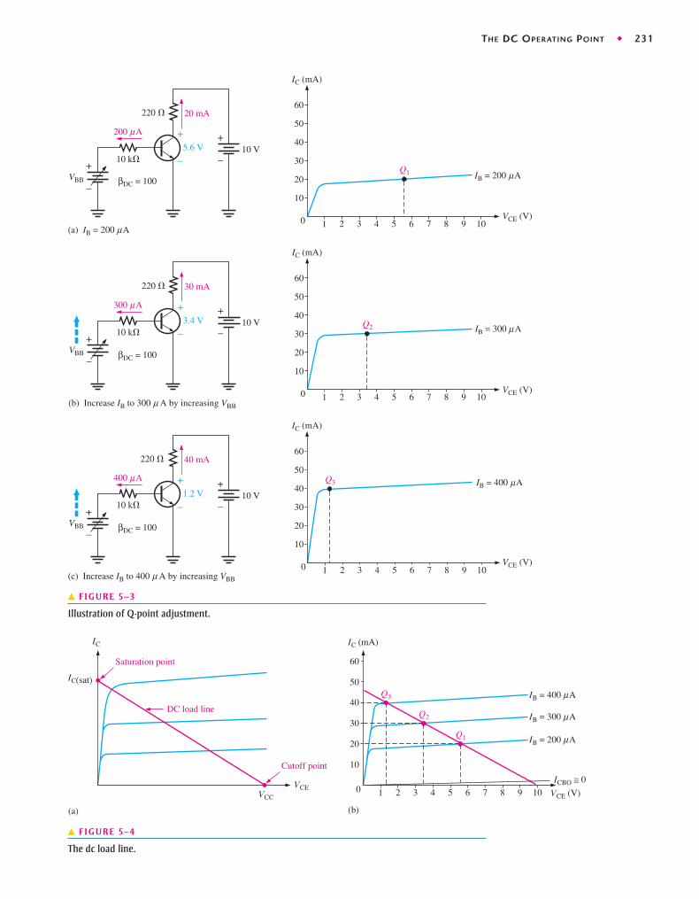
F Y IIn Figure 5–3, we assign three values to IB and observe what happens to IC and VCE.
First, VBB is adjusted to produce an IB of as shown in Figure 5–3(a). Sincethe collector current is 20 mA, as indicated, and
This Q-point is shown on the graph of Figure 5–3(a) as Q1.Next, as shown in Figure 5–3(b), VBB is increased to produce an IB of and an IC
of 30 mA.
The Q-point for this condition is indicated by Q2 on the graph.Finally, as in Figure 5–3(c), VBB is increased to give an IB of and an IC of
40 mA.
is the corresponding Q-point on the graph.
DC Load Line The dc operation of a transistor circuit can be described graphicallyusing a dc load line. This is a straight line drawn on the characteristic curves from thesaturation value where IC IC(sat) on the y-axis to the cutoff value where VCE VCCon the x-axis, as shown in Figure 5–4(a). The load line is determined by the externalcircuit (VCC and RC), not the transistor itself, which is described by the characteristiccurves.
In Figure 5–3, the equation for IC is
This is the equation of a straight line with a slope of �1 RC, an x intercept of VCE VCC,and a y intercept of VCC RC, which is IC(sat).> =>
IC =VCC - VCE
RC=
VCC
RC-
VCE
RC= -
VCE
RC+
VCC
RC= - a 1
RCbVCE +
VCC
RC
==
Q3
VCE = 10 V - (40 mA)(220 Æ) = 10 V - 8.8 V = 1.2 V
400 mA
VCE = 10 V - (30 mA)(220 Æ) = 10 V - 6.6 V = 3.4 V
300 mA
VCE = VCC - ICRC = 10 V - (20 mA)(220 Æ) = 10 V - 4.4 V = 5.6 V
IC = bDC IB,200 mA,
THE DC OPERATING POINT ◆ 231
400 Aμ
200 Aμ
μ
μ
300 Aμ
IB = 200 Aμ
–
+
VBB
10 V5.6 V
–
+
20 mA
(a) IB =
10
20
30
40
50
60
1 2 3 4 5 6 7 8 9 100 VCE (V)
IC (mA)
–
+
–
+
VBB
10 V3.4 V
–
+
30 mA
(b) Increase IB to 300 A by increasing VBB
10
20
30
40
50
60
1 2 3 4 5 6 7 8 9 100 VCE (V)
IB = 300 A
IC (mA)
–
+
–
+
VBB
10 V1.2 V
–
+
40 mA
(c) Increase IB to 400 A by increasing VBB
10
20
30
40
50
60
1 2 3 4 5 6 7 8 9 100 VCE (V)
IB = 400 A
IC (mA)
–
+
Q1
Q2
Q3
220 �
220 �
10 k�
220 �
10 k�
10 k�
βDC = 100
βDC = 100
βDC = 100
μ
μ
200 Aμ
� FIGURE 5–3
Illustration of Q-point adjustment.
IB = 300 A
IB = 400 Aμ
10
20
30
40
1 2 3 4 5 6 7 8 9 100 VCE (V)
IC (mA)
IB = 200 A
50
60
Q3
Q1
Q2
ICBO ≅ 0
μ
μ
(b)
VCC
VCE
IC
IC(sat)
Saturation point
Cutoff point
DC load line
(a)
� FIGURE 5–4
The dc load line.

232 ◆ TRANSISTOR BIAS CIRCUITS
The point at which the load line intersects a characteristic curve represents the Q-pointfor that particular value of IB. Figure 5–4(b) illustrates the Q-point on the load line for eachvalue of IB in Figure 5–3.
Linear Operation The region along the load line including all points between saturationand cutoff is generally known as the linear region of the transistor’s operation. As long asthe transistor is operated in this region, the output voltage is ideally a linear reproductionof the input.
Figure 5–5 shows an example of the linear operation of a transistor. AC quantities areindicated by lowercase italic subscripts. Assume a sinusoidal voltage, Vin, is superimposedon VBB, causing the base current to vary sinusoidally above and below its Q-pointvalue of This, in turn, causes the collector current to vary 10 mA above and belowits Q-point value of 30 mA. As a result of the variation in collector current, the collector-to-emitter voltage varies 2.2 V above and below its Q-point value of 3.4 V. Point A on theload line in Figure 5–5 corresponds to the positive peak of the sinusoidal input voltage.Point B corresponds to the negative peak, and point Q corresponds to the zero value of thesine wave, as indicated. VCEQ, ICQ, and IBQ are dc Q-point values with no input sinusoidalvoltage applied.
300 mA.100 mA
3.4VCEQ
–
+
10 k�
VBB
VCC
10 V
220 �
–
+3.7 V
Vin
VBB – 0.7 V
RB=
VceIBQ =
RB
RC
βDC = 100
3.7 V – 0.7 V
10 k�= 300 A
ICQ = βDC IBQ = (100)(300 A) = 30 mA
VCEQ = VCC – ICQ RC = 10 V – (30 mA)(220 �) = 3.4 V
Ib
μ
μ
IB = 300 A
IB = 400 Aμ
10
20
30
4045.5
1.2 5.6 100 VCE
VCC
(V)
IC (mA)
IB = 200 A
50
60
A
B
Q μ
μ
Ic
� FIGURE 5–5
Variations in collector current and collector-to-emitter voltage as a result of a variation in base current.
Waveform Distortion As previously mentioned, under certain input signal conditionsthe location of the Q-point on the load line can cause one peak of the Vce waveform to belimited or clipped, as shown in parts (a) and (b) of Figure 5–6. In each case the input sig-nal is too large for the Q-point location and is driving the transistor into cutoff or saturationduring a portion of the input cycle. When both peaks are limited as in Figure 5–6(c), thetransistor is being driven into both saturation and cutoff by an excessively large input sig-nal. When only the positive peak is limited, the transistor is being driven into cutoff but notsaturation. When only the negative peak is limited, the transistor is being driven into satu-ration but not cutoff.
Gordon Moore, one of the foundersof Intel, observed in an article inthe April, 1965, issue of Electronicsmagazine that innovations intechnology would allow a doublingof the number of transistors in agiven space every year (in an updatearticle in 1975, Moore adjusted therate to every two years to accountfor the growing complexity ofchips), and that the speed of thosetransistors would increase. Thisprediction has become widelyknown as Moore’s law.
F Y I

THE DC OPERATING POINT ◆ 233
Saturation
IC
ICQ Q
0 VCC
VCE
VCEQ
Saturation
I BQ
Vce
VCCVCE
Cutoff
Q
I BQ
IC
ICQ
Cutoff 0
Vce
VCEQ
(a) Transistor is driven into saturation because the Q-point istoo close to saturation for the given input signal.
VCEQ
VCC
VCE
I BQ
Cutoff
Cutoff
Q
0
Saturation
IC
ICQ
Saturation
Vce
Inputsignal
Inputsignal
Inputsignal
(b) Transistor is driven into cutoff because the Q-point istoo close to cutoff for the given input signal.
(c) Transistor is driven into both saturation and cutoff because theinput signal is too large.
� FIGURE 5–6
Graphical load line illustration of a transistor being driven into saturation and/or cutoff.
Determine the Q-point for the circuit in Figure 5–7 and draw the dc load line. Find themaximum peak value of base current for linear operation. Assume
Solution The Q-point is defined by the values of IC and VCE.
VCE = VCC - ICRC = 20 V - 13.07 V = 6.93 V
IC = bDCIB = (200)(198 mA) = 39.6 mA
IB =VBB - VBE
RB=
10 V - 0.7 V
47 kÆ= 198 mA
bDC = 200.EXAMPLE 5–1

234 ◆ TRANSISTOR BIAS CIRCUITS
The Q-point is at IC 39.6 mA and at VCE 6.93 V.Since IC(cutoff ) 0, you need to know IC(sat) to determine how much variation in
collector current can occur and still maintain linear operation of the transistor.
The dc load line is graphically illustrated in Figure 5–8, showing that before satura-tion is reached, IC can increase an amount ideally equal to
However, IC can decrease by 39.6 mA before cutoff (IC 0) is reached. Therefore,the limiting excursion is 21 mA because the Q-point is closer to saturation than to cut-off. The 21 mA is the maximum peak variation of the collector current. Actually, itwould be slightly less in practice because VCE(sat) is not quite zero.
=
IC(sat) - ICQ = 60.6 mA - 39.6 mA = 21.0 mA
IC(sat) =VCC
RC=
20 V
330 Æ= 60.6 mA
===
IC (mA)
VCE (V)
60.6
39.6
06.93 20
Ideal saturation
Ideal cutoff
Q
� FIGURE 5–8
–
+
RB
47 k�
RC330 �
VBB10 V
VCC20 V–
+
� FIGURE 5–7
Determine the maximum peak variation of the base current as follows:
Related Problem* Find the Q-point for the circuit in Figure 5–7, and determine the maximum peak value ofbase current for linear operation for the following circuit values:
Open the Multisim file E05-01 in the Examples folder on the companion website.Measure IC and VCE and compare with the calculated values.
1.0 kÆ, and VCC = 24 V.bDC = 100, RC =
Ib( peak) =Ic( peak)
bDC=
21 mA
200= 105 MA
*Answers can be found at www.pearsonhighered.com/floyd.

VOLTAGE-DIVIDER BIAS ◆ 235
1. What are the upper and lower limits on a dc load line in terms of VCE and IC?
2. Define Q-point.
3. At what point on the load line does saturation occur? At what point does cutoff occur?
4. For maximum Vce, where should the Q-point be placed?
SECTION 5–1 CHECKUPAnswers can be found at www.pearsonhighered.com/floyd.
5–2 VOLTAGE-DIVIDER BIAS
You will now study a method of biasing a transistor for linear operation using a single-source resistive voltage divider. This is the most widely used biasing method. Fourother methods are covered in Section 5–3.
After completing this section, you should be able to
❏ Analyze a voltage-divider biased circuit◆ Define the term stiff voltage-divider ◆ Calculate currents and voltages in avoltage-divider biased circuit
❏ Explain the loading effects in voltage-divider bias◆ Describe how dc input resistance at the transistor base affects the bias
❏ Apply Thevenin’s theorem to the analysis of voltage-divider bias◆ Analyze both npn and pnp circuits
+VCC
RCR1
RER2
I2 + IB
I2
AIB
IE
IC
� FIGURE 5–9
Voltage-divider bias.
Up to this point a separate dc source, VBB, was used to bias the base-emitter junction be-cause it could be varied independently of VCC and it helped to illustrate transistor opera-tion. A more practical bias method is to use VCC as the single bias source, as shown inFigure 5–9. To simplify the schematic, the battery symbol is omitted and replaced by a linetermination circle with a voltage indicator (VCC) as shown.
A dc bias voltage at the base of the transistor can be developed by a resistive voltage-divider that consists of R1 and R2, as shown in Figure 5–9. VCC is the dc collector supplyvoltage. Two current paths are between point A and ground: one through R2 and the otherthrough the base-emitter junction of the transistor and RE.
Generally, voltage-divider bias circuits are designed so that the base current is muchsmaller than the current (I2) through R2 in Figure 5–9. In this case, the voltage-divider cir-cuit is very straightforward to analyze because the loading effect of the base current can beignored. A voltage divider in which the base current is small compared to the current in R2is said to be a stiff voltage divider because the base voltage is relatively independent ofdifferent transistors and temperature effects.
To analyze a voltage-divider circuit in which IB is small compared to I2, first calculatethe voltage on the base using the unloaded voltage-divider rule:
VB � a R2
R1 � R2bVCC
Equation 5–1
Equation 5–2
Equation 5–3
Once you know the base voltage, you can find the voltages and currents in the circuit, asfollows:
VE � VB � VBE
and
IC � IE �VE
RE
Then,VC � VCC � ICRC Equation 5–4

236 ◆ TRANSISTOR BIAS CIRCUITS
Determine VCE and IC in the stiff voltage-divider biased transistor circuit of Figure 5–10if bDC = 100.
EXAMPLE 5–2
RC1.0 k�
VCC+10 V
R110 k�
RE560 �
R25.6 k�
� FIGURE 5–10
Solution The base voltage is
So,
and
Therefore,
and
Related Problem If the voltage divider in Figure 5–10 was not stiff, how would VB be affected?
Open the Multisim file E05-02 in the Examples folder on the companion website.Measure IC and VCE. If these results do not agree very closely with those in theExample, what original assumption was incorrect?
VCE = VC - VE = 4.84 V - 2.89 V = 1.95 V
VC = VCC - ICRC = 10 V - (5.16 mA)(1.0 kÆ) = 4.84 V
IC � IE = 5.16 mA
IE =VE
RE=
2.89 V
560 Æ= 5.16 mA
VE = VB - VBE = 3.59 V - 0.7 V = 2.89 V
VB � a R2
R1 + R2bVCC = a 5.6 kÆ
15.6 kÆb10 V = 3.59 V
The basic analysis developed in Example 5–2 is all that is needed for most voltage-divider circuits, but there may be cases where you need to analyze the circuit with more ac-curacy. Ideally, a voltage-divider circuit is stiff, which means that the transistor does notappear as a significant load. All circuit design involves trade-offs; and one trade-off is thatstiff voltage dividers require smaller resistors, which are not always desirable because ofpotential loading effects on other circuits and added power requirements. If the circuitdesigner wanted to raise the input resistance, the divider string may not be stiff; and moredetailed analysis is required to calculate circuit parameters. To determine if the divider is stiff,you need to examine the dc input resistance looking in at the base as shown in Figure 5–11.
Once you know VC and VE, you can determine VCE.
VCE = VC - VE

VOLTAGE-DIVIDER BIAS ◆ 237
R1
+VCC
R2
VB
RIN(BASE)
R IN(BASE) looking inat base of transistor
RIN(BASE) � 10R2
RIN(BASE) < 10R2
Stiff:
Not stiff:
VB ≅ VCCR2
R1 + R2
VB = VCCR2 �� RIN(BASE)
R1 + R2 �� RIN(BASE)
� FIGURE 5–11
Voltage divider with load.
Loading Effects of Voltage-Divider Bias
DC Input Resistance at the Transistor Base The dc input resistance of the transistor isproportional to so it will change for different transistors. When a transistor is operat-ing in its linear region, the emitter current (IE) is When the emitter resistor isviewed from the base circuit, the resistor appears to be larger than its actual value becauseof the dc current gain in the transistor. That is, RIN(BASE) = VB IB = VB (IE DC).
RIN(BASE) �BDCVB
IE
b>>>bDCIB.
bDC,
Equation 5–5
This is the effective load on the voltage divider illustrated in Figure 5–11.You can quickly estimate the loading effect by comparing RIN(BASE) to the resistor R2 in
the voltage divider. As long as RIN(BASE) is at least ten times larger than R2, the loadingeffect will be 10% or less and the voltage divider is stiff. If RIN(BASE) is less than ten timesR2, it should be combined in parallel with R2.
Determine the dc input resistance looking in at the base of the transistor in Figure5–12. and VB = 4 V.bDC = 125
EXAMPLE 5–3
+VCC
RC560 �
RE1.0 k�
VB
4 V
� FIGURE 5–12
Solution
Related Problem What is RIN(BASE) in Figure 5–12 if and VB = 2 V?bDC = 60
RIN(BASE) =bDCVB
IE=
125(4 V)
3.3 mA= 152 kæ
IE =VB - 0.7 V
RE=
3.3 V
1.0 kÆ= 3.3 mA
238 ◆ TRANSISTOR BIAS CIRCUITS
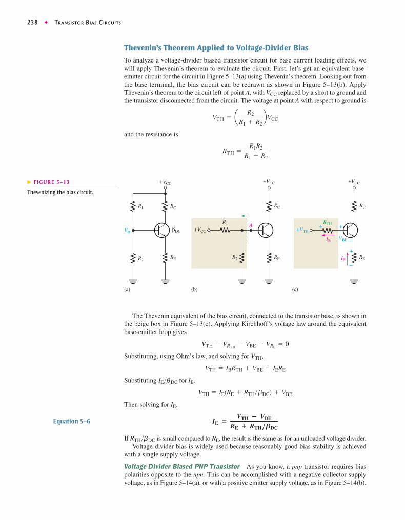
Thevenin’s Theorem Applied to Voltage-Divider Bias
To analyze a voltage-divider biased transistor circuit for base current loading effects, wewill apply Thevenin’s theorem to evaluate the circuit. First, let’s get an equivalent base-emitter circuit for the circuit in Figure 5–13(a) using Thevenin’s theorem. Looking out fromthe base terminal, the bias circuit can be redrawn as shown in Figure 5–13(b). ApplyThevenin’s theorem to the circuit left of point A, with VCC replaced by a short to ground andthe transistor disconnected from the circuit. The voltage at point A with respect to ground is
and the resistance is
RT H =R1R2
R1 + R2
VT H = a R2
R1 + R2bVCC
+VCC
RCR1
VB βDC
(a)
RC
R1
+VCC
RERE R2R2
+VCC
(b)
RC
RTH
+VCC
RE
+VTH
(c)
+ –
IB
+
+
–
–IE
VBE
A
� FIGURE 5–13
Thevenizing the bias circuit.
The Thevenin equivalent of the bias circuit, connected to the transistor base, is shown inthe beige box in Figure 5–13(c). Applying Kirchhoff’s voltage law around the equivalentbase-emitter loop gives
Substituting, using Ohm’s law, and solving for VTH,
Substituting
Then solving for IE,
IE �VTH � VBE
RE � RTH/BDC
VTH = IE(RE + RTH>bDC) + VBE
IE>bDC for IB,
VTH = IBRTH + VBE + IERE
VTH - VRTH- VBE - VRE
= 0
Equation 5–6
If is small compared to RE, the result is the same as for an unloaded voltage divider.Voltage-divider bias is widely used because reasonably good bias stability is achieved
with a single supply voltage.
Voltage-Divider Biased PNP Transistor As you know, a pnp transistor requires biaspolarities opposite to the npn. This can be accomplished with a negative collector supplyvoltage, as in Figure 5–14(a), or with a positive emitter supply voltage, as in Figure 5–14(b).
RTH>bDC

VOLTAGE-DIVIDER BIAS ◆ 239
In a schematic, the pnp is often drawn upside down so that the supply voltage is at the topof the schematic and ground at the bottom, as in Figure 5–14(c).
The analysis procedure is the same as for an npn transistor circuit using Thevenin’s the-orem and Kirchhoff’s voltage law, as demonstrated in the following steps with reference toFigure 5–14. For Figure 5–14(a), applying Kirchhoff’s voltage law around the base-emit-ter circuit gives
By Thevenin’s theorem,
The base current is
The equation for IE is
IE ��VTH � VBE
RE � RTH/BDC
IB =IE
bDC
RTH =R1R2
R1 + R2
VTH = a R2
R1 + R2bVCC
VTH + IBRTH - VBE + IERE = 0
RC
−VCC
R1
RER2
(a) Negative collector supply voltage, VCC
RCR1
RER2
+VEE
(b) Positive emitter supply voltage, VEE
(c) The circuit in (b) redrawn
RE
+VEE
R2
RCR1
+–VBE VE
VB
VC
� FIGURE 5–14
Voltage-divider biased pnp transistor.
Equation 5–7
For Figure 5–14(b), the analysis is as follows:
The equation for IE is
IE �VTH � VBE � VEE
RE � RTH/BDC
IB =IE
bDC
RTH =R1R2
R1 + R2
VTH = a R1
R1 + R2bVEE
-VTH + IBRTH - VBE + IERE - VEE = 0
Equation 5–8

240 ◆ TRANSISTOR BIAS CIRCUITS
Solution This circuit has the configuration of Figures 5–14(b) and (c). Apply Thevenin’stheorem.
Use Equation 5–8 to determine IE.
The negative sign on IE indicates that the assumed current direction in the Kirchhoff’sanalysis is opposite from the actual current direction. From IE, you can determine ICand VEC as follows:
Related Problem Determine for Figure 5–15.
Open the Multisim file E05-04 in the Examples folder on the companion website.Measure IC and VEC.
RIN(BASE)
VEC = VE - VC = 7.68 V - 5.08 V = 2.6 V
VE = VEE - IERE = 10 V - (2.31 mA)(1.0 kÆ) = 7.68 V
VC = ICRC = (2.31 mA)(2.2 kÆ) = 5.08 V
IC = IE = 2.31 mA
=-2.42 V
1.0459 kÆ= -2.31 mAIE =
VTH + VBE - VEE
RE + RTH>bDC=
6.88 V + 0.7 V - 10 V
1.0 kÆ + 45.9 Æ
RTH =R1R2
R1 + R2=
(22 kÆ)(10 kÆ)
22 kÆ + 10 kÆ= 6.88 kÆ
VTH = a R1
R1 + R2bVEE = a 22 kÆ
22 kÆ + 10 kÆb10 V = (0.688)10 V = 6.88 V
Find IC and VEC for the pnp transistor circuit in Figure 5–15.EXAMPLE 5–4
RE1.0 k�
VEE+10 V
R210 k�
RC2.2 k�
R122 k�
βDC = 150
� FIGURE 5–15
Find IC and VCE for a pnp transistor circuit with these values: Refer to Figure
5–14(a), which shows the schematic with a negative supply voltage.
Solution Apply Thevenin’s theorem.
= (0.409)(-6 V) = -2.45 V
VTH = a R2
R1 + R2bVCC = a 47 kÆ
68 kÆ + 47 kÆb (-6 V)
47 kÆ, RC = 1.8 kÆ, RE = 2.2 kÆ, VCC = -6 V, and bDC = 75.R1 = 68 kÆ, R2 =EXAMPLE 5–5
OTHER BIAS METHODS ◆ 241
Use Equation 5–7 to determine IE.
From IE, you can determine IC and VCE as follows:
Related Problem What value of is required in this example in order to neglect RIN(BASE) in keepingwith the basic ten-times rule for a stiff voltage divider?
bDC
VCE = VC - VE = -3.79 V + 2.71 V = �1.08 V
VE = -IERE = -(1.23 mA)(2.2 kÆ) = -2.71 V
VC = -VCC + ICRC = -6 V + (1.23 mA)(1.8 kÆ) = -3.79 V
IC = IE = 1.23 mA
=3.15 V
2.57 kÆ= 1.23 mA
IE =-VTH + VBE
RE + RTH>bDC=
2.45 V + 0.7 V
2.2 kÆ + 371 Æ
RTH =R1R2
R1 + R2=
(68 kÆ)(47 kÆ)
(68 kÆ + 47 kÆ)= 27.8 kÆ
1. If the voltage at the base of a transistor is 5 V and the base current is A, what is thedc input resistance at the base?
2. If a transistor has a dc beta of 190, VB 2 V, and IE 2 mA, what is the dc inputresistance at the base?
3. What bias voltage is developed at the base of a transistor if both resistors in a stiffvoltage divider are equal and
4. What are two advantages of voltage-divider bias?
VCC � �10 V?
��
5 mSECTION 5–2 CHECKUP
5–3 OTHER BIAS METHODS
In this section, four additional methods for dc biasing a transistor circuit are discussed.Although these methods are not as common as voltage-divider bias, you should be ableto recognize them when you see them and understand the basic differences.
After completing this section, you should be able to
❏ Analyze four more types of bias circuits❏ Discuss emitter bias
◆ Analyze an emitter-biased circuit❏ Discuss base bias
◆ Analyze a base-biased circuit ◆ Explain Q-point stability of base bias❏ Discuss emitter-feedback bias
◆ Define negative feedback ◆ Analyze an emitter-feedback biased circuit❏ Discuss collector-feedback bias
◆ Analyze a collector-feedback biased circuit ◆ Discuss Q-point stability overtemperature
Emitter Bias
Emitter bias provides excellent bias stability in spite of changes in or temperature. It usesboth a positive and a negative supply voltage. To obtain a reasonable estimate of the key dcvalues in an emitter-biased circuit, analysis is quite easy. In an npn circuit, such as shown
b

242 ◆ TRANSISTOR BIAS CIRCUITS
in Figure 5–17, the small base current causes the base voltage to be slightly below ground.The emitter voltage is one diode drop less than this. The combination of this small dropacross RB and VBE forces the emitter to be at approximately Using this approxima-tion, you can obtain the emitter current as
VEE is entered as a negative value in this equation.You can apply the approximation that to calculate the collector voltage.
The approximation that is useful for troubleshooting because you won’t needto perform any detailed calculations. As in the case of voltage-divider bias, there is a morerigorous calculation for cases where you need a more exact result.
VE � -1 V
VC = VCC - ICRC
IC � IE
IE =-VEE - 1 V
RE
-1 V.
Calculate IE and VCE for the circuit in Figure 5–16 using the approximationsVE � -1 V and IC � IE.
EXAMPLE 5–6
Solution
Related Problem If VEE is changed to what is the new value of VCE?-12 V,
VCE = 8.4 V - (-1) = 9.4 V
VC = VCC - ICRC = +15 V - (1.4 mA)(4.7 kÆ) = 8.4 V
IE =-VEE - 1 V
RE=
-(-15 V) - 1 V
10 kÆ=
14 V
10 kÆ= 1.4 mA
VE � -1 V
RE10 k�
VCC+15 V
RC4.7 k�
RB
47 k�
VEE–15 V
� FIGURE 5–16
The approximation that and the neglect of may not be accurateenough for design work or detailed analysis. In this case, Kirchhoff’s voltage law can beapplied as follows to develop a more detailed formula for IE. Kirchhoff’s voltage law ap-plied around the base-emitter circuit in Figure 5–17(a), which has been redrawn in part (b)for analysis, gives the following equation:
Substituting, using Ohm’s law,
VEE + IBRB + VBE + IERE = 0
VEE + VRB+ VBE + VRE
= 0
bDCVE � -1 V

OTHER BIAS METHODS ◆ 243
Substituting for and transposing
Factoring out IE and solving for IE,
IE ��VEE � VBE
RE � RB/BDC
a IE
bDCbRB + IERE + VBE = -VEE
VEE,IB � IE>bDC
Equation 5–9
Voltages with respect to ground are indicated by a single subscript. The emitter voltagewith respect to ground is
The base voltage with respect to ground is
The collector voltage with respect to ground is
VC = VCC - ICRC
VB = VE + VBE
VE = VEE + IERE
VEE
VCC
RC
RB
REVB
VE VC
RCIC
+
–
RE
+
–
+–VBE
RB
IB
VEE
IE
+ –
(a) (b)
VCC� FIGURE 5–17
An npn transistor with emitter bias.Polarities are reversed for a pnp tran-sistor. Single subscripts indicate volt-ages with respect to ground.
Determine how much the Q-point (IC, VCE) for the circuit in Figure 5–18 will changeif increases from 100 to 200 when one transistor is replaced by another.bDC
EXAMPLE 5–7
RE10 k�
VCC+15 V
RC4.7 k�
RB
47 k�
VEE–15 V
� FIGURE 5–18

244 ◆ TRANSISTOR BIAS CIRCUITS
Solution For
Therefore,
For
Therefore,
The percent change in IC as changes from 100 to 200 is
The percent change in is
Related Problem Determine the Q-point in Figure 5–18 if increases to 300.bDC
%¢VCE = aVCE(2) - VCE(1)
VCE(1)b100% = a9.71 V - 9.83 V
9.83 Vb100% = �1.22%
VCE
%¢IC = a IC(2) - IC(1)
IC(1)b100% = a1.38 mA - 1.37 mA
1.37 mAb100% = 0.730%
bDC
VCE(2) = VC - VE = 8.51 V - (-1.2 V) = 9.71 V
VE = VEE + IERE = -15 V + (1.38 mA)(10 kÆ) = -1.2 V
VC = VCC - IC(2)RC = 15 V - (1.38 mA)(4.7 kÆ) = 8.51 V
IC(2) � IE =-VEE - VBE
RE + RB>bDC=
-(-15 V) - 0.7 V
10 kÆ + 47 kÆ>200= 1.38 mA
bDC = 200,
VCE(1) = VC - VE = 8.56 V - (-1.3 V) = 9.83 V
VE = VEE + IERE = -15 V + (1.37 mA)(10 kÆ) = -1.3 V
VC = VCC - IC(1)RC = 15 V - (1.37 mA)(4.7 kÆ) = 8.56 V
IC(1) � IE =-VEE - VBE
RE + RB>bDC=
-(-15 V) - 0.7 V
10 kÆ + 47 kÆ>100= 1.37 mA
bDC = 100,
Base Bias
This method of biasing is common in switching circuits. Figure 5–19 shows a base-biasedtransistor. The analysis of this circuit for the linear region shows that it is directly depend-ent on Starting with Kirchhoff’s voltage law around the base circuit,
Substituting IBRB for you get
Then solving for IB,
Kirchhoff’s voltage law applied around the collector circuit in Figure 5–19 gives the fol-lowing equation:
Solving for VCE,
VCE � VCC � ICRC
VCC - ICRC - VCE = 0
IB =VCC - VBE
RB
VCC - IBRB - VBE = 0
VRB,
VCC - VRB- VBE = 0
bDC.
Equation 5–10
Substituting the expression for IB into the formula yields
IC � BDCaVCC � VBE
RBb
IC = bDCIB
Equation 5–11
RC
RB
VBE
+
+VCC
VCE
+
––
� FIGURE 5–19
Base bias.

OTHER BIAS METHODS ◆ 245
Q-Point Stability of Base Bias Notice that Equation 5–11 shows that IC is dependenton The disadvantage of this is that a variation in causes IC and, as a result, VCEto change, thus changing the Q-point of the transistor. This makes the base bias circuitextremely beta-dependent and unpredictable.
Recall that varies with temperature and collector current. In addition, there is alarge spread of values from one transistor to another of the same type due to manu-facturing variations. For these reasons, base bias is rarely used in linear circuits but is dis-cussed here so you will be familiar with it.
bDC
bDC
bDCbDC.
Determine how much the Q-point (IC, VCE) for the circuit in Figure 5–20 will changeover a temperature range where increases from 100 to 200.bDC
EXAMPLE 5–8
RC560 �
RB
VCC+12 V
330 k�
� FIGURE 5–20
Solution For
The percent change in IC as changes from 100 to 200 is
The percent change in VCE is
As you can see, the Q-point is very dependent on in this circuit and thereforemakes the base bias arrangement very unreliable. Consequently, base bias is not nor-mally used if linear operation is required. However, it can be used in switchingapplications.
Related Problem Determine IC if increases to 300.bDC
bDC
= a8.17 V - 10.1 V
10.1 Vb100% = �19.1% (a decrease)
%¢VCE = aVCE(2) - VCE(1)
VCE(1)b100%
= a6.84 mA - 3.42 mA
3.42 mAb100% = 100% (an increase)
%¢IC = a IC(2) - IC(1)
IC(1)b100%
bDC
VCE(2) = VCC - IC(2) RC = 12 V - (6.84 mA)(560 Æ) = 8.17 V
IC(2) = bDCaVCC - VBE
RBb = 200a12 V - 0.7 V
330 kÆb = 6.84 mA
For bDC = 200,
VCE(1) = VCC - IC(1)RC = 12 V - (3.42 mA)(560 Æ) = 10.1 V
IC(1) = bDCaVCC - VBE
RBb = 100a12 V - 0.7 V
330 kÆb = 3.42 mA
bDC = 100,

246 ◆ TRANSISTOR BIAS CIRCUITS
Emitter-Feedback Bias
If an emitter resistor is added to the base-bias circuit in Figure 5–20, the result is emitter-feedback bias, as shown in Figure 5–21. The idea is to help make base bias more pre-dictable with negative feedback, which negates any attempted change in collector currentwith an opposing change in base voltage. If the collector current tries to increase, the emit-ter voltage increases, causing an increase in base voltage because VB VE + VBE. This in-crease in base voltage reduces the voltage across RB, thus reducing the base current andkeeping the collector current from increasing. A similar action occurs if the collector cur-rent tries to decrease. While this is better for linear circuits than base bias, it is still de-pendent on and is not as predictable as voltage-divider bias. To calculate IE, you canwrite Kirchhoff’s voltage law (KVL) around the base circuit.
Substituting for IB, you can see that IE is still dependent on
IE �VCC � VBE
RE � RB/BDC
bDC.IE>bDC
-VCC + IBRB + VBE + IERE = 0
bDC
=
Open the Multisim file E05-08 in the Examples folder on the companion website.Set and measure IC and VCE. Next, set and measure ICand VCE. Compare results with the calculated values.
bDC = 200bDC = 100
RC
RE
RB
VCC
� FIGURE 5–21
Emitter-feedback bias.
Equation 5–12
The base-bias circuit from Example 5–8 is converted to emitter-feedback bias by theaddition of a emitter resistor. All other values are the same, and a transistor witha is used. Determine how much the Q-point will change if the first transis-tor is replaced with one having a Compare the results to those of thebase-bias circuit.
Solution For
For
The percent change in IC is
Although the emitter-feedback bias significantly improved the stability of the bias fora change in compared to base bias, it still does not provide a reliable Q-point.
Related Problem Determine IC if a transistor with is used in the circuit.bDC = 300
bDC
%¢VCE = aVCE(2) - VCE(1)
VCE(1)b100% = a7.90 V - 5.35 V
7.90 Vb100% = �32.3%
%¢IC = a IC(2) - IC(1)
IC(1)b100% = a4.26 mA - 2.63 mA
2.63 mAb100% = 62.0%
VCE(2) = VCC - IC(2)(RC + RE) = 12 V - (4.26 mA)(560 Æ + 1 kÆ) = 5.35 V
IC(2) = IE =VCC - VBE
RE + RB>bDC=
12 V - 0.7 V
1 kÆ + 330 kÆ>200= 4.26 mA
bDC = 200,
VCE(1) = VCC - IC(1)(RC + RE) = 12 V - (2.63 mA)(560 Æ + 1 kÆ) = 7.90 V
IC(1) = IE =VCC - VBE
RE + RB>bDC=
12 V - 0.7 V
1 kÆ + 330 kÆ>100 = 2.63 mA
bDC = 100,
bDC = 200.bDC = 100
1 kÆEXAMPLE 5–9
OTHER BIAS METHODS ◆ 247
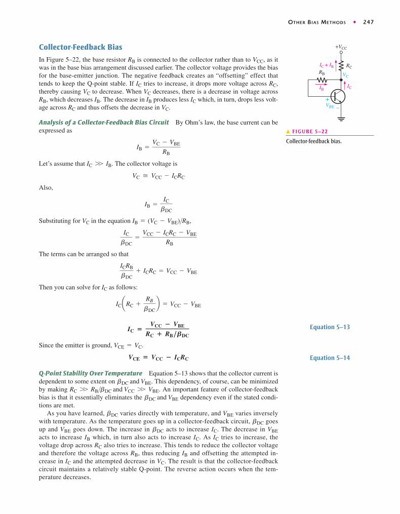
Collector-Feedback Bias
In Figure 5–22, the base resistor RB is connected to the collector rather than to VCC, as itwas in the base bias arrangement discussed earlier. The collector voltage provides the biasfor the base-emitter junction. The negative feedback creates an “offsetting” effect thattends to keep the Q-point stable. If IC tries to increase, it drops more voltage across RC,thereby causing VC to decrease. When VC decreases, there is a decrease in voltage acrossRB, which decreases IB. The decrease in IB produces less IC which, in turn, drops less volt-age across RC and thus offsets the decrease in VC.
Analysis of a Collector-Feedback Bias Circuit By Ohm’s law, the base current can beexpressed as
Let’s assume that The collector voltage is
Also,
Substituting for VC in the equation
The terms can be arranged so that
Then you can solve for IC as follows:
IC �VCC � VBE
RC � RB/BDC
ICaRC +RB
bDCb = VCC - VBE
ICRB
bDC+ ICRC = VCC - VBE
IC
bDC=
VCC - ICRC - VBE
RB
IB = (VC - VBE)>RB,
IB =IC
bDC
VC � VCC - ICRC
IC W IB.
IB =VC - VBE
RB
Equation 5–13
Since the emitter is ground, VCE VC.
VCE � VCC � ICRC
=
Equation 5–14
Q-Point Stability Over Temperature Equation 5–13 shows that the collector current isdependent to some extent on This dependency, of course, can be minimizedby making An important feature of collector-feedbackbias is that it essentially eliminates the dependency even if the stated condi-tions are met.
As you have learned, varies directly with temperature, and VBE varies inverselywith temperature. As the temperature goes up in a collector-feedback circuit, goesup and VBE goes down. The increase in acts to increase IC. The decrease in VBEacts to increase IB which, in turn also acts to increase IC. As IC tries to increase, thevoltage drop across RC also tries to increase. This tends to reduce the collector voltageand therefore the voltage across RB, thus reducing IB and offsetting the attempted in-crease in IC and the attempted decrease in VC. The result is that the collector-feedbackcircuit maintains a relatively stable Q-point. The reverse action occurs when the tem-perature decreases.
bDC
bDC
bDC
bDC and VBE
RC W RB>bDC and VCC W VBE.bDC and VBE.
RC
+VCC
+–VBE
IC + IB
IC
VCRB
IB
� FIGURE 5–22
Collector-feedback bias.

248 ◆ TRANSISTOR BIAS CIRCUITS
Calculate the Q-point values (IC and VCE) for the circuit in Figure 5–23.EXAMPLE 5–10
RC10 k�
VCC+10 V
RB
180 k�
+–0.7 V
βDC = 100
� FIGURE 5–23
Solution Using Equation 5–13, the collector current is
Using Equation 5–14, the collector-to-emitter voltage is
Related Problem Calculate the Q-point values in Figure 5–23 for and determine the percentchange in the Q-point from
Open the Multisim file E05-10 in the Examples folder on the companion website.Measure IC and VCE. Compare with the calculated values.
bDC = 100 to bDC = 200.bDC = 200
VCE = VCC - ICRC = 10 V - (788 mA)(10 kÆ) = 2.12 V
IC =VCC - VBE
RC + RB>bDC=
10 V - 0.7 V
10 kÆ + 180 kÆ>100= 788 MA
1. Why is emitter bias more stable than base bias?
2. What is the main disadvantage of emitter bias?
3. Explain how an increase in causes a reduction in base current in a collector-feed-back circuit.
4. What is the main disadvantage of the base bias method?
5. Explain why the base bias Q-point changes with temperature.
6. How does emitter-feedback bias improve on base bias?
bDC
SECTION 5–3 CHECKUP
5–4 TROUBLESHOOTING
In a biased transistor circuit, the transistor can fail or a resistor in the bias circuit canfail. We will examine several possibilities in this section using the voltage-divider biasarrangement. Many circuit failures result from open resistors, internally open transistorleads and junctions, or shorted junctions. Often, these failures can produce an apparentcutoff or saturation condition when voltage is measured at the collector.
After completing this section, you should be able to
❏ Troubleshoot faults in transistor bias circuits❏ Troubleshoot a voltage-divider biased transistor circuit
◆ Troubleshoot the circuit for several common faults ◆ Use voltage measurementto isolate a fault
TROUBLESHOOTING ◆ 249
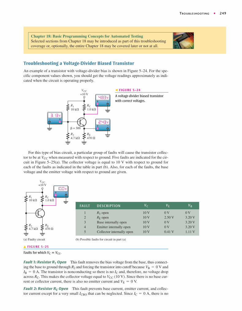
Troubleshooting a Voltage-Divider Biased Transistor
An example of a transistor with voltage-divider bias is shown in Figure 5–24. For the spe-cific component values shown, you should get the voltage readings approximately as indi-cated when the circuit is operating properly.
For this type of bias circuit, a particular group of faults will cause the transistor collec-tor to be at VCC when measured with respect to ground. Five faults are indicated for the cir-cuit in Figure 5–25(a). The collector voltage is equal to 10 V with respect to ground foreach of the faults as indicated in the table in part (b). Also, for each of the faults, the basevoltage and the emitter voltage with respect to ground are given.
Fault 1: Resistor R1 Open This fault removes the bias voltage from the base, thus connect-ing the base to ground through R2 and forcing the transistor into cutoff because VB 0 V andIB 0 A. The transistor is nonconducting so there is no IC and, therefore, no voltage dropacross RC. This makes the collector voltage equal to VCC (10 V). Since there is no base cur-rent or collector current, there is also no emitter current and VE 0 V.
Fault 2: Resistor RE Open This fault prevents base current, emitter current, and collec-tor current except for a very small ICBO that can be neglected. Since IC 0 A, there is no=
=
==
V–+
V–+
V–
R110 k�
RC1.0 k�
R24.7 k�
RE470 �
VCC+10 V
� = 300
+
� FIGURE 5–24
A voltage-divider biased transistorwith correct voltages.
V–+
R110 k�
RC1.0 k�
R24.7 k�
RE470 �
VCC+10 V
(a) Faulty circuit (b) Possible faults for circuit in part (a)
FAULT DESCRIPTION VC VE VB
10 V10 V10 V10 V10 V
0 V2.50 V0 V0 V0.41 V
0 V3.20 V3.20 V3.20 V1.11 V
12345
R1 openRE openBase internally openEmitter internally openCollector internally open
� FIGURE 5–25
Faults for which VC � VCC.
Chapter 18: Basic Programming Concepts for Automated TestingSelected sections from Chapter 18 may be introduced as part of this troubleshootingcoverage or, optionally, the entire Chapter 18 may be covered later or not at all.

250 ◆ TRANSISTOR BIAS CIRCUITS
voltage drop across RC and, therefore, VC = VCC = 10 V. The voltage divider produces avoltage at the base with respect to ground as follows:
When a voltmeter is connected to the emitter, it provides a current path through its highinternal impedance, resulting in a forward-biased base-emitter junction. Therefore, theemitter voltage is The amount of the forward voltage drop across the BEjunction depends on the current. VBE = 0.7 V is assumed for purposes of illustration, but itmay be much less. The result is an emitter voltage as follows:
Fault 3: Base Internally Open An internal transistor fault is more likely to happen thanan open resistor. Again, the transistor is nonconducting so IC � 0 A and VC � VCC � 10 V.Just as for the case of the open RE, the voltage divider produces 3.2 V at the external baseconnection. The voltage at the external emitter connection is 0 V because there is no emit-ter current through RE and, thus, no voltage drop.
Fault 4: Emitter Internally Open Again, the transistor is nonconducting, so IC � 0 Aand VC � VCC � 10 V. Just as for the case of the open RE and the internally open base, thevoltage divider produces 3.2 V at the base. The voltage at the external emitter lead is 0 Vbecause that point is open and connected to ground through RE. Notice that Faults 3 and 4produce identical symptoms.
Fault 5: Collector Internally Open Since there is an internal open in the transistor col-lector, there is no IC and, therefore, VC � VCC � 10 V. In this situation, the voltage divider isloaded by RE through the forward-biased BE junction, as shown by the approximate equiva-lent circuit in Figure 5–26. The base voltage and emitter voltage are determined as follows:
VE = VB - VBE = 1.11 V - 0.7 V = 0.41 V
= a 427 Æ10.427 kÆ
b10 V + 0.7 V = 0.41 V + 0.7 V = 1.11 V
VB � a R2 7RE
R1 + R2 7REbVCC + 0.7 V
VE = VB - VBE = 3.2 V - 0.7 V = 2.5 V
VE = VB - VBE.
VB = a R2
R1 + R2bVCC = a 4.7 kÆ
14.7 kÆb10 V = 3.20 V
VCC+10 V
R110 k�
RE470 �
R24.7 k�
VB VE
Diode equivalent of BE junction
� FIGURE 5–26
Equivalent bias circuit for an inter-nally open collector.
There are two possible additional faults for which the transistor is conducting or appears to be conducting, based on the collector voltage measurement. These are indicatedin Figure 5–27.
Fault 6: Resistor RC Open For this fault, which is illustrated in Figure 5–27(a), the col-lector voltage may lead you to think that the transistor is in saturation, but actually it is

TROUBLESHOOTING ◆ 251
nonconducting. Obviously, if RC is open, there can be no collector current. In this situation,the equivalent bias circuit is the same as for Fault 5, as illustrated in Figure 5–26.Therefore, VB � 1.11 V and since the BE junction is forward-biased,
When a voltmeter is connected to the collector to measure VC, a current path is providedthrough the internal impedance of the meter and the BC junction is forward-biased by VB.Therefore,
Again the forward drops across the internal transistor junctions depend on the current.We are using 0.7 V for illustration, but the forward drops may be much less.
Fault 7: Resistor R2 Open When R2 opens as shown in Figure 5–27(b), the base voltageand base current increase from their normal values because the voltage divider is nowformed by and In this case, the base voltage is determined by the emittervoltage
First, verify whether the transistor is in saturation or not. The collector saturation cur-rent and the base current required to produce saturation are determined as follows (assum-ing VCE(sat) � 0.2 V):
Assuming the transistor is saturated, the maximum base current is determined.
Since this amount of base current is more than enough to produce saturation, the transistoris definitely saturated. Therefore, VE, VB, and VC are as follows:
VC = VCC - IC(sat)RC = 10 V - (6.67 mA)(1.0 kÆ) = 3.33 V
VB = 3.83 V
VE = 3.13 V
IB =VCC
R1 + RIN(BASE)=
10 V
182 kÆ= 54.9 mA
RIN(BASE) =BDCVB
IE=
(300)(3.83 V)
6.67 mA= 172 kÆ
VB = VE + VBE = 3.83 V
VE = IE(sat)RE = 3.13 V
IE(sat) � 6.67 mA
IB(sat) =IC(sat)
bDC=
6.67 mA
300= 22.2 mA
IC(sat) =VCC - VCE(sat)
RC + RE=
9.8 V
1.47 kÆ= 6.67 mA
(VB = VE + VBE).RIN(BASE).R1
VC = VB - VBC = 1.11 V - 0.7 V = 0.41 V
VE = VB - VBE = 1.11 V - 0.7 V = 0.41 V
−+
−+
− +
R110 k�
RC1.0 k�
R24.7 k�
RE470 �
VCC+10 V
� = 300
(a) RC open
R110 k�
RC1.0 k�
R24.7 k�
RE470 �
VCC+10 V
� = 300
(b) R2 open
− +
−+
−+
mV
mV
V V
V
V
� FIGURE 5–27
Faults for which the transistor is con-ducting or appears to be conducting.

252 ◆ TRANSISTOR BIAS CIRCUITS
Multisim Troubleshooting Exercises
These file circuits are in the Troubleshooting Exercises folder on the companion website.Open each file and determine if the circuit is working properly. If it is not workingproperly, determine the fault.
1. Multisim file TSE05-01
2. Multisim file TSE05-02
3. Multisim file TSE05-03
4. Multisim file TSE05-04
5. Multisim file TSE05-05
1. How do you determine when a transistor is saturated? When a transistor is in cutoff?
2. In a voltage-divider biased npn transistor circuit, you measure VCC at the collector andan emitter voltage 0.7 V less than the base voltage. Is the transistor functioning in cut-off, or is RE open?
3. What symptoms does an open RC produce?
SECTION 5–4 CHECKUP
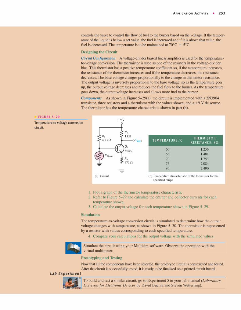
Application Activity: Temperature to Voltage Conversion
The focus of this Application Activity is a temperature-sensing circuit that converts the tem-perature of a liquid to a proportional voltage for the purpose of maintaining the temperatureof the liquid within a specified range. Figure 5–28 illustrates the temperature-control system.The temperature sensor is a thermistor, which is a device whose resistance changes withtemperature. The thermistor is connected to a transistor circuit that is biased for linear opera-tion. The output voltage of the circuit is proportional to the thermistor resistance and thus tothe temperature of the liquid in the tank. The output voltage goes to an interface circuit that
Valveinterface
Temperature-to-voltageconversioncircuit
DC powersupply
Thermistor
Continuouslyvariable valve
Fuel flow
� FIGURE 5–28
Temperature-control system.
APPLICATION ACTIVIT Y ◆ 253
controls the valve to control the flow of fuel to the burner based on the voltage. If the temper-ature of the liquid is below a set value, the fuel is increased and if it is above that value, thefuel is decreased. The temperature is to be maintained at
Designing the Circuit
Circuit Configuration A voltage-divider biased linear amplifier is used for the temperature-to-voltage conversion. The thermistor is used as one of the resistors in the voltage-dividerbias. This thermistor has a positive temperature coefficient so, if the temperature increases,the resistance of the thermistor increases and if the temperature decreases, the resistance decreases. The base voltage changes proportionally to the change in thermistor resistance.The output voltage is inversely proportional to the base voltage, so as the temperature goesup, the output voltage decreases and reduces the fuel flow to the burner. As the temperaturegoes down, the output voltage increases and allows more fuel to the burner.
Components As shown in Figure 5–29(a), the circuit is implemented with a 2N3904transistor, three resistors and a thermistor with the values shown, and a +9 V dc source.The thermistor has the temperature characteristic shown in part (b).
70°C ; 5°C.
R3
RTherm
VOUT
470 �
Q1
2N3904
+9 V
R21 k�
(a) Circuit
R14.7 k�
(b) Temperature characteristic of the thermistor for the specified range
T
TEMPERATURE,�CTHERMISTOR
RESISTANCE, k�
1.2561.4811.7532.0842.490
6065707580
� FIGURE 5–29
Temperature-to-voltage conversioncircuit.
1. Plot a graph of the thermistor temperature characteristic.2. Refer to Figure 5–29 and calculate the emitter and collector currents for each
temperature shown.3. Calculate the output voltage for each temperature shown in Figure 5–29.
Simulation
The temperature-to-voltage conversion circuit is simulated to determine how the outputvoltage changes with temperature, as shown in Figure 5–30. The thermistor is representedby a resistor with values corresponding to each specified temperature.
4. Compare your calculations for the output voltage with the simulated values.
Simulate the circuit using your Multisim software. Observe the operation with thevirtual multimeter.
Prototyping and Testing
Now that all the components have been selected, the prototype circuit is constructed and tested.After the circuit is successfully tested, it is ready to be finalized on a printed circuit board.
To build and test a similar circuit, go to Experiment 5 in your lab manual (LaboratoryExercises for Electronic Devices by David Buchla and Steven Wetterling).
Lab Experiment
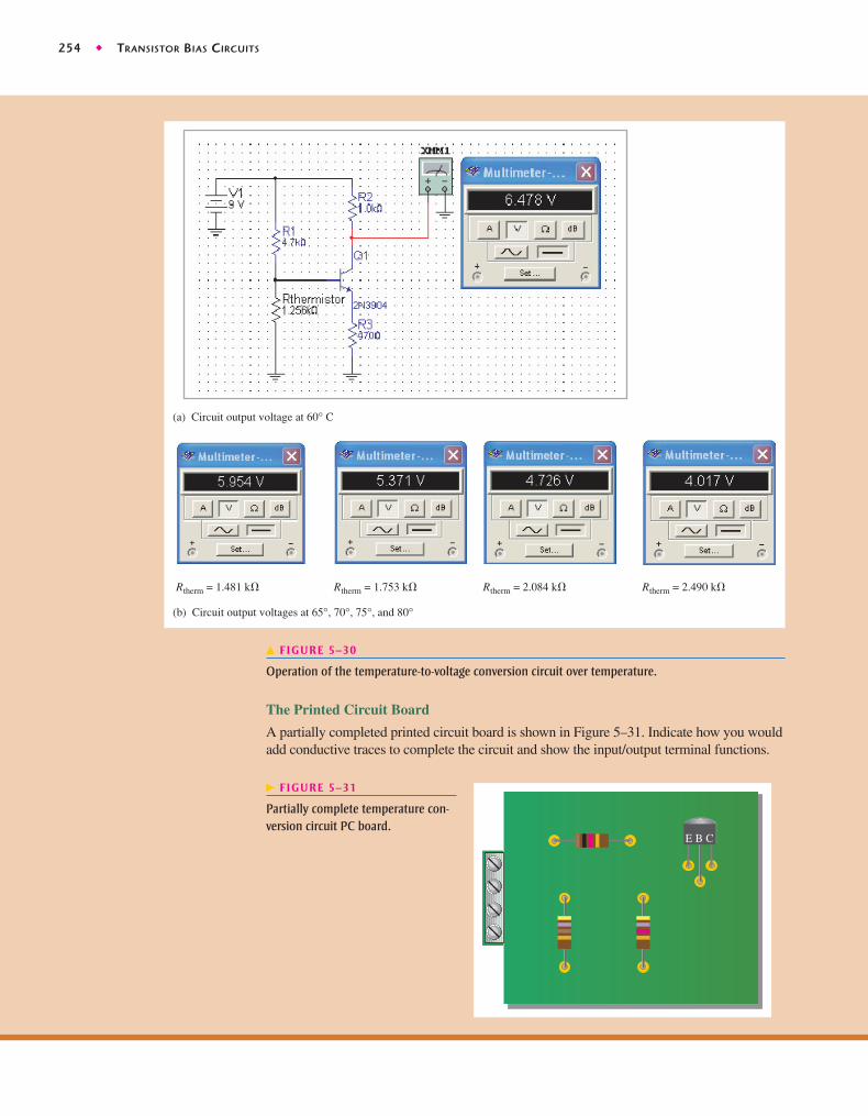
254 ◆ TRANSISTOR BIAS CIRCUITS
(a) Circuit output voltage at 60° C
(b) Circuit output voltages at 65°, 70°, 75°, and 80°
Rtherm = 1.481 k� Rtherm = 1.753 k� Rtherm = 2.084 k� Rtherm = 2.490 k�
� FIGURE 5–30
Operation of the temperature-to-voltage conversion circuit over temperature.
The Printed Circuit Board
A partially completed printed circuit board is shown in Figure 5–31. Indicate how you wouldadd conductive traces to complete the circuit and show the input/output terminal functions.
E B C
� FIGURE 5–31
Partially complete temperature con-version circuit PC board.
SUMMARY OF TRANSISTOR BIAS CIRCUITS ◆ 255
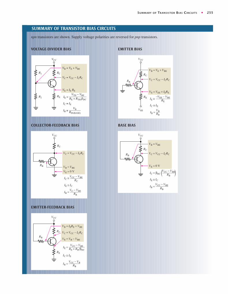
SUMMARY OF TRANSISTOR BIAS CIRCUITS
npn transistors are shown. Supply voltage polarities are reversed for pnp transistors.
VOLTAGE-DIVIDER BIAS EMITTER BIAS
COLLECTOR-FEEDBACK BIAS BASE BIAS
EMITTER-FEEDBACK BIAS
RC
IC ≅ IE
VC = VCC − ICRC
VTH − VBE
RE + RTH/βDC
VE = IE RE
VCC
R1
RER2
VB = VE + VBE
IE =
IB ≅VB
RIN(BASE)
VCC
RC
RB
IE ≅ IC
VC = VCC − ICRC
VB = VBE
VE = 0 V
IB =VC − VBE
RB
IC ≅VCC − VBE
RC
RC
RB
VCC
IE ≅ IC
VC = VCC − ICRC
VB = VBE
VE = 0 V
IC = βDCVCC − VBB
RB
IB =VCC − VBE
RB
RC
RE
RB
VCC
IC ≅ IE
VC = VCC − ICRC
VE = VB − VBE
VB = IERE + VBE
IE =VCC − VBE
RE + RB/βDC
IB =VCC − VB
RB
RC
RB
VCC
RE
VEE
IC ≅ IE
VC = VCC − ICRC
VB = VE + VBE
VE = VEE + IERE
IB =VBRB
IE ≅−VEE − VBE
RE

256 ◆ TRANSISTOR BIAS CIRCUITS
SUMMARY
Section 5–1 ◆ The purpose of biasing a circuit is to establish a proper stable dc operating point (Q-point).
◆ The Q-point of a circuit is defined by specific values for IC and VCE. These values are called thecoordinates of the Q-point.
◆ A dc load line passes through the Q-point on a transistor’s collector curves intersecting the verti-cal axis at approximately IC(sat) and the horizontal axis at VCE(off).
◆ The linear (active) operating region of a transistor lies along the load line below saturation andabove cutoff.
Section 5–2 ◆ Loading effects are neglected for a stiff voltage divider.
◆ The dc input resistance at the base of a BJT is approximately
◆ Voltage-divider bias provides good Q-point stability with a single-polarity supply voltage. It isthe most common bias circuit.
Section 5–3 ◆ Emitter bias generally provides good Q-point stability but requires both positive and negativesupply voltages.
◆ The base bias circuit arrangement has poor stability because its Q-point varies widely with
◆ Emitter-feedback bias combines base bias with the addition of an emitter resistor.
◆ Collector-feedback bias provides good stability using negative feedback from collector to base.
KEY TERMS Key terms and other bold terms in the chapter are defined in the end-of-book glossary.
DC load line A straight line plot of IC and VCE for a transistor circuit.
Feedback The process of returning a portion of a circuit’s output back to the input in such a way asto oppose or aid a change in the output.
Linear region The region of operation along the load line between saturation and cutoff.
Q-point The dc operating (bias) point of an amplifier specified by voltage and current values.
Stiff voltage divider A voltage divider for which loading effects can be neglected.
KEY FORMULAS
Voltage-Divider Bias
5–1 for a stiff voltage divider
5–2
5–3
5–4
5–5
5–6
5–7
5–8
Emitter Bias
5–9 IE ��VEE � VBE
RE � RB/BDC
IE �VTH � VBE � VEE
RE � RTH/BDC
IE ��VTH � VBE
RE � RTH/BDC
IE �VTH � VBE
RE � RTH/BDC
RIN(BASE) �BDCVB
IE
VC � VCC � ICRC
IC � IE �VE
RE
VE � VB � VBE
VB � a R2
R1 � R2bVCC
bDC.
bDCRE.

CIRCUIT-ACTION QUIZ ◆ 257
Base Bias
5–10
5–11
Emitter-Feedback Bias
5–12
Collector-Feedback Bias
5–13
5–14
TRUE/FALSE QUIZ Answers can be found at www.pearsonhighered.com/floyd.
1. DC bias establishes the dc operating point for an amplifier.
2. Q-point is the quadratic point in a bias circuit.
3. The dc load line intersects the horizontal axis of a transistor characteristic curve at VCE � VCC.
4. The dc load line intersects the vertical axis of a transistor characteristic curve at IC � 0.
5. The linear region of a transistor’s operation lies between saturation and cutoff.
6. Voltage-divider bias is rarely used.
7. Input resistance at the base of the transistor can affect voltage-divider bias.
8. Stiff voltage-divider bias is essentially independent of base loading.
9. Emitter bias uses one dc supply voltage.
10. Negative feedback is employed in collector-feedback bias.
11. Base bias is less stable than voltage-divider bias.
12. A pnp transistor requires bias voltage polarities opposite to an npn transistor.
CIRCUIT-ACTION QUIZ Answers can be found at www.pearsonhighered.com/floyd.
1. If VBB in Figure 5–7 is increased, the Q-point value of collector current will
(a) increase (b) decrease (c) not change
2. If VBB in Figure 5–7 is increased, the Q-point value of VCE will
(a) increase (b) decrease (c) not change
3. If the value of R2 in Figure 5–10 is reduced, the base voltage will
(a) increase (b) decrease (c) not change
4. If the value of R1 in Figure 5–10 is increased, the emitter current will
(a) increase (b) decrease (c) not change
5. If RE in Figure 5–15 is decreased, the collector current will
(a) increase (b) decrease (c) not change
6. If RB in Figure 5–18 is reduced, the base-to-emitter voltage will
(a) increase (b) decrease (c) not change
7. If VCC in Figure 5–20 is increased, the base-to-emitter voltage will
(a) increase (b) decrease (c) not change
8. If R1 in Figure 5–24 opens, the collector voltage will
(a) increase (b) decrease (c) not change
9. If R2 in Figure 5–24 opens, the collector voltage will
(a) increase (b) decrease (c) not change
10. If R2 in Figure 5–24 is increased, the emitter current will
(a) increase (b) decrease (c) not change
VCE � VCC � ICRC
IC �VCC � VBE
RC � RB/BDC
IE �VCC � VBE
RE � RB/BDC
IC � BDC aVCC � VBE
RBb
VCE � VCC � ICRC

258 ◆ TRANSISTOR BIAS CIRCUITS
SELF-TEST Answers can be found at www.pearsonhighered.com/floyd.
Section 5–1 1. The maximum value of collector current in a biased transistor is
(a) (b) IC(sat) (c) greater than IE (d)
2. Ideally, a dc load line is a straight line drawn on the collector characteristic curves between
(a) the Q-point and cutoff (b) the Q-point and saturation
(c) VCE(cutoff) and IC(sat) (d)
3. If a sinusoidal voltage is applied to the base of a biased npn transistor and the resulting sinu-soidal collector voltage is clipped near zero volts, the transistor is
(a) being driven into saturation (b) being driven into cutoff
(c) operating nonlinearly (d) answers (a) and (c)
(e) answers (b) and (c)
Section 5–2 4. The input resistance at the base of a biased transistor depends mainly on
(a) (b) RB (c) RE (d)
5. In a voltage-divider biased transistor circuit such as in Figure 5–13, RIN(BASE) can generally beneglected in calculations when
(a) (b) (c) (d)
6. In a certain voltage-divider biased npn transistor, VB is 2.95 V. The dc emitter voltage is ap-proximately
(a) 2.25 V (b) 2.95 V (c) 3.65 V (d) 0.7 V
7. Voltage-divider bias
(a) cannot be independent of (b) can be essentially independent of
(c) is not widely used (d) requires fewer components than all the other methods
Section 5–3 8. Emitter bias is
(a) essentially independent of (b) very dependent on
(c) provides a stable bias point (d) answers (a) and (c)
9. In an emitter bias circuit, The emitter current
(a) is 5.3 mA (b) is 2.7 mA
(c) is 180 mA (d) cannot be determined
10. The disadvantage of base bias is that
(a) it is very complex (b) it produces low gain
(c) it is too beta dependent (d) it produces high leakage current
11. Collector-feedback bias is
(a) based on the principle of positive feedback (b) based on beta multiplication
(c) based on the principle of negative feedback (d) not very stable
Section 5–4 12. In a voltage-divider biased npn transistor, if the upper voltage-divider resistor (the one con-nected to VCC) opens,
(a) the transistor goes into cutoff (b) the transistor goes into saturation
(c) the transistor burns out (d) the supply voltage is too high
13. In a voltage-divider biased npn transistor, if the lower voltage-divider resistor (the one con-nected to ground) opens,
(a) the transistor is not affected (b) the transistor may be driven into cutoff
(c) the transistor may be driven into saturation (d) the collector current will decrease
14. In a voltage-divider biased pnp transistor, there is no base current, but the base voltage is ap-proximately correct. The most likely problem(s) is
(a) a bias resistor is open (b) the collector resistor is open
(c) the base-emitter junction is open (d) the emitter resistor is open
(e) answers (a) and (c) (f) answers (c) and (d)
RE = 2.7 kÆ and VEE = 15 V.
bDCbDC
bDCbDC
R1 V R2RIN(BASE) 7 10R2R2 7 10RIN(BASE)RIN(BASE) 7 R2
bDC and REbDC
IB = 0 and IB = IC>bDC
IE - IBbDCIB

PROBLEMS ◆ 259
15. If R1 in Figure 5–25 is open, the base voltage is
(a) +10 V (b) 0 V (c) 3.13 V (d) 0.7 V
16. If R1 is open, the collector current in Figure 5–25 is
(a) 5.17 mA (b) 10 mA (c) 4.83 mA (d) 0 mA
PROBLEMS Answers to all odd-numbered problems are at the end of the book.
BASIC PROBLEMSSection 5–1 The DC Operating Point
1. The output (collector voltage) of a biased transistor amplifier is shown in Figure 5–32. Is thetransistor biased too close to cutoff or too close to saturation?
� FIGURE 5–32
≈ 0 V
2. What is the Q-point for a biased transistor as in Figure 5–2 with
3. What is the saturation value of collector current in Problem 2?
4. What is the cutoff value of VCE in Problem 2?
5. Determine the intercept points of the dc load line on the vertical and horizontal axes of the collector-characteristic curves for the circuit in Figure 5–33.
VCC = 18 V, and RC = 1.0 kÆ?IB = 150 mA, bDC = 75,
� FIGURE 5–33
Multisim file circuits are identifiedwith a logo and are in the Problemsfolder on the companion website.Filenames correspond to figure num-bers (e.g., F05-33).
6. Assume that you wish to bias the transistor in Figure 5–33 with To what voltagemust you change the VBB supply? What are IC and VCE at the Q-point, given that
7. Design a biased-transistor circuit using VBB = VCC = 10 V for a Q-point of IC � 5 mA and VCE� 4 V. Assume The design involves finding RB, RC, and the minimum power ratingof the transistor. (The actual power rating should be greater.) Sketch the circuit.
8. Determine whether the transistor in Figure 5–34 is biased in cutoff, saturation, or the linear region. Remember that is valid only in the linear region.IC = bDCIB
bDC = 100.
bDC = 50?IB = 20 mA.
RC10 k�
RB
–
+VBB10 V
1.0 M� –
+VCC20 V
RC390 �
RB
VCC+8 V
10 k�
VBB1.5 V
βDC = 75
� FIGURE 5–34

260 ◆ TRANSISTOR BIAS CIRCUITS
� FIGURE 5–35
20
30
40
50
60
1 2 3 4 5 6 7 8 9
Q-point
10VCE (V)
100 A
200 A
300 A
400 A
500 A
600 A
IC (mA)
0
10 μ
μ
μ
μ
μ
μ
9. From the collector characteristic curves and the dc load line in Figure 5–35, determine the following:
(a) Collector saturation current
(b) VCE at cutoff
(c) Q-point values of IB, IC, and VCE
10. From Figure 5–35 determine the following:
(a) Maximum collector current for linear operation
(b) Base current at the maximum collector current
(c) VCE at maximum collector current
Section 5–2 Voltage-Divider Bias
11. What is the minimum value of in Figure 5–36 that makes
12. The bias resistor R2 in Figure 5–36 is replaced by a potentiometer. What minimum re-sistance setting causes saturation?
13. If the potentiometer described in Problem 12 is set at what are the values for IC and VCE?
14. Determine all transistor terminal voltages with respect to ground in Figure 5–37.
15. Show the connections required to replace the transistor in Figure 5–37 with a pnp device.
16. (a) Determine VB in Figure 5–38.
(b) How is VB affected if the transistor is replaced by one with a
17. Determine the following in Figure 5–38:
(a) Q-point values
(b) The minimum power rating of the transistor
18. Determine I1, I2, and IB in Figure 5–38.
bDC of 50?
2 kÆ,
15 kÆRIN(BASE) G 10R2?bDC
RC1.5 k�
+15 V
βDC = 150
RE680 �
R24.7 k�
R122 k�
RC2.2 k�
+9 V
βDC = 110
RE1.0 k�
R215 k�
R147 k�
� FIGURE 5–36
� FIGURE 5–37
RC1.8 k�
VCC–12 V
βDC = 150
RE560 �
R25.6 k�
R133 k�
� FIGURE 5–38

25. What value of RC can be used to decrease IC in Problem 24 by 25 percent?
26. What is the minimum power rating for the transistor in Problem 25?
27. A collector-feedback circuit uses an npn transistor with Determine the collector current and the collector voltage if
28. Determine IB, IC, and VCE for a base-biased transistor circuit with the following values:VCC = 12 V,
29. If in Problem 28 doubles over temperature, what are the Q-point values?
30. You have two base bias circuits connected for testing. They are identical except that one is biased with a separate VBB source and the other is biased with the base resistor connected to VCC.Ammeters are connected to measure collector current in each circuit. You vary the VCC supplyvoltage and observe that the collector current varies in one circuit, but not in the other. In whichcircuit does the collector current change? Explain your observation.
31. The datasheet for a particular transistor specifies a minimum of 50 and a maximum of 125. What range of Q-point values can be expected if an attempt is made to mass-producethe circuit in Figure 5–42? Is this range acceptable if the Q-point must remain in the transis-tor’s linear region?
32. The base bias circuit in Figure 5–42 is subjected to a temperature variation from The decreases by 50 percent at and increases by 75 percent at from its nominalvalue of 110 at What are the changes in IC and VCE over the temperature range of0°C to 70°C?
25°C.70°C0°CbDC
0°C to 70°C.
bDCbDC
bDC
RB = 22 kÆ, and RC = 100 Æ.bDC = 90,
bDC = 200.RB = 47 kÆ.VCC = 12 V, RC = 1.2 kÆ, and
PROBLEMS ◆ 261
Section 5–3 Other Bias Methods
19. Analyze the circuit in Figure 5–39 to determine the correct voltages at the transistor terminalswith respect to ground. Assume
20. To what value can RE in Figure 5–39 be reduced without the transistor going into saturation?
21. Taking VBE into account in Figure 5–39, how much will IE change with a temperature increasefrom The VBE is 0.7 V at and decreases 2.5 mV per degree Celsius.Neglect any change in
22. When can the effect of a change in be neglected in the emitter bias circuit?
23. Determine IC and VCE in the pnp emitter bias circuit of Figure 5–40. Assume
24. Determine VB, VC, and IC in Figure 5–41.
bDC = 100.
bDC
bDC.25°C25°C to 100°C?
bDC = 100.
RE470 �
RB
VEE+10 V
10 k�
RC330 �
–10 VVCC
RC1.8 k�
VCC+3 V
RB
33 k�βDC = 90
VCC
+5 V
RC1.0 k�
RB
10 k�
RE2.2 k�
–5 VVEE
� FIGURE 5–39
� FIGURE 5–40 � FIGURE 5–41
� FIGURE 5–42
RC100 �
VCC+9 V
RB15 k�

262 ◆ TRANSISTOR BIAS CIRCUITS
Section 5–4 Troubleshooting
33. Determine the meter readings in Figure 5–43 if R1 is open.
− +
−+
−+
R1
V1
V2
V3
33 k�RC2.2 k�
R210 k�
RE1.0 k�
VCC+8 V
�DC = 200
� FIGURE 5–43
� FIGURE 5–44
− +
−+
−+
− +
−+
−+
− +
−+
−+
− +
−+
−+
R110 k�
RC1.0 k�
R21.0 k�
RE100 �
VCC+12 V
�DC = 180
(a)
R1100 k�
RC10 k�
R210 k�
RE1.0 k�
VCC+20 V
�DC = 200
(b)
R112 k�
RC680 �
R227 k�
RE1.5 k�
VCC+10 V
�DC = 100
(c)
R18.2 k�
RC1.0 k�
R222 k�
RE3.3 k�
VCC+9 V
�DC = 120
(d)
V
V
mV
V
V
V
V
V
V
V
VV
34. Assume the emitter becomes shorted to ground in Figure 5–43 by a solder splash or stray wireclipping. What do the meters read? When you correct the problem, what do the meters read?
35. Determine the most probable failures, if any, in each circuit of Figure 5–44, based on the indi-cated measurements.
36. Determine if the DMM readings 2 through 4 in the breadboard circuit of Figure 5–45 are cor-rect. If they are not, isolate the problem(s). The transistor is a pnp device with a specified dcbeta range of 35 to 100.

PROBLEMS ◆ 263
37. Determine each meter reading in Figure 5–45 for each of the following faults:
(a) the resistor open (b) the resistor open
(c) the resistor open (d) the resistor open
(e) a short from emitter to ground (f) an open base-emitter junction
APPLICATION ACTIVITY PROBLEMS38. Determine VB, VE, and VC in the temperature-to-voltage conversion circuit in Figure 5–29(a) if
R1 fails open.
39. What faults will cause the transistor in the temperature-to-voltage conversion circuit to go intocutoff?
40. A thermistor with the characteristic curve shown in Figure 5–46 is used in the circuit of Figure5–29(a). Calculate the output voltage for temperatures of Assume a stiffvoltage divider.
41. Explain how you would identify an open collector-base junction in the transistor in Figure 5–29(a).
45°C, 48°C, and 53°C.
1.0 kÆ10 kÆ5.6 kÆ680 Æ
4
DCV
V �COM
5 1
3
DCV
V �COM
4 1
2
DCV
V �COM
3 1
1
DCV
V �COM
2 1
E B C
2
3 5
1
4
V V V V
� FIGURE 5–45
2.6
2.4
2.2
2.0
1.8
1.6
1.4
45 46 47 48 49 50 51 52 53 54 55T (°C)
R (k�)� FIGURE 5–46

264 ◆ TRANSISTOR BIAS CIRCUITS
DATASHEET PROBLEMS42. Analyze the temperature-to-voltage conversion circuit in Figure 5–47 at the temperature ex-
tremes indicated on the graph in Figure 5–46 for both minimum and maximum specifieddatasheet values of hFE. Refer to the partial datasheet in Figure 5–48.
43. Verify that no maximum ratings are exceeded in the temperature-to-voltage conversion circuitin Figure 5–47. Refer to the partial datasheet in Figure 5–48.
44. Refer to the partial datasheet in Figure 5–49.
(a) What is the maximum collector current for a 2N2222A?
(b) What is the maximum reverse base-emitter voltage for a 2N2218A?
45. Determine the maximum power dissipation for a 2N2222A at
46. When you increase the collector current in a 2N2219A from 1 mA to 500 mA, how much doesthe minimum (hFE) change?
ADVANCED PROBLEMS47. Design a circuit using base bias that operates from a 15 V dc voltage and draws a maximum
current from the dc source (ICC(max)) of 10 mA. The Q-point values are to be IC � 5 mA andVCE � 5 V. The transistor is a 2N3904. Assume a midpoint value for bDC.
bDC
100°C.
RC1.0 k�
VCC+9.1 V
R15.6 k�
RE470 �
2N3904
T R2
Output
Absolute Maximum Ratings* TA = 25°C unless otherwise noted
*These ratings are limiting values above which the serviceability of any semiconductor device may be impaired.
NOTES:1) These ratings are based on a maximum junction temperature of 150 degrees C.2) These are steady state limits. The factory should be consulted on applications involving pulsed or low duty cycle operations.
Symbol Parameter Value Units
VCEO Collector-Emitter Voltage 40 V
VCBO Collector-Base Voltage 60 V
VEBO Emitter-Base Voltage 6.0 V
IC Collector Current - Continuous 200 mA
TJ, Tstg Operating and Storage Junction Temperature Range -55 to +150 °C
ON CHARACTERISTICS*hFE DC Current Gain IC = 0.1 mA, VCE = 1.0 V
IC = 1.0 mA, VCE = 1.0 VIC = 10 mA, VCE = 1.0 VIC = 50 mA, VCE = 1.0 VIC = 100 mA, VCE = 1.0 V
40701006030
300
VCE(sat) Collector-Emitter Saturation Voltage IC = 10 mA, IB = 1.0 mAIC = 50 mA, IB = 5.0 mA
0.20.3
VV
VBE(sat) Base-Emitter Saturation Voltage IC = 10 mA, IB = 1.0 mAIC = 50 mA, IB = 5.0 mA
0.65 0.850.95
VV
� FIGURE 5–47
� FIGURE 5–48
Partial datasheet for the 2N3904transistor. Copyright FairchildSemiconductor Corporation. Used by permission.

PROBLEMS ◆ 265
Maximum Ratings
Rating
Collector-Emitter voltageCollector-Base voltageEmitter-Base voltageCollector current — continuous
Total device dissipation @ TA = 25°C Derate above 25°CTotal device dissipation @ TC = 25°C Derate above 25°COperating and storage junction Temperature range
SymbolVCEO
VCBO
VEBO
IC
PD
PD
2N22182N22192N22212N2222
30605.0800
Unit
WattmW/°C
0.84.57
3.017.1
TJ, Tstg
2N2218,A2N2219,A
2N2218A2N2219A2N2221A2N2222A
40756.0800
0.52.28
1.26.85
2N2221,A2N2222,A
2N55812N5582
40756.0800
0.63.33
2.011.43
2N55812N5582
WattmW/°C
°C–65 to +200
V dcV dcV dc
mA dc
Electrical Characteristics (TA = 25°C unless otherwise noted.)
Characteristic Symbol Max UnitMin
Off CharacteristicsCollector-Emitter breakdown voltage (IC = 10 mA dc, IB = 0)
Collector-Base breakdown voltage (IC = 10 A dc, IE = 0)
Emitter-Base breakdown voltage (IE = 10 A dc, IC = 0)
Collector cutoff current (VCE = 60 V dc, VEB(off) = 3.0 V dcCollector cutoff current (VCB = 50 V dc, IE = 0) (VCB = 60 V dc, IE = 0) (VCB = 50 V dc, IE = 0, TA = 150°C) (VCB = 60 V dc, IE = 0, TA = 150°C)Emitter cutoff current (VEB = 3.0 V dc, IC = 0)Base cutoff current (VCE = 60 V dc, VEB(off) = 3.0 V dc)
V(BR)CEO
V(BR)CBO
V(BR)EBO
ICEX
ICBO
IEBO
IBL
V dc
V dc
V dc
nA dc
A dc
nA dc
nA dc
3040
6075
5.06.0
—
————
—
—
——
——
——
10
0.010.01101010
20
Non-A SuffixA-Suffix, 2N5581, 2N5582
Non-A SuffixA-Suffix, 2N5581, 2N5582
Non-A SuffixA-Suffix, 2N5581, 2N5582
A-Suffix, 2N5581, 2N5582
Non-A SuffixA-Suffix, 2N5581, 2N5582Non-A SuffixA-Suffix, 2N5581, 2N5582
A-Suffix, 2N5581, 2N5582
A-Suffix
On CharacteristicsDC current gain (IC = 0.1 mA dc, VCE = 10 V dc)
(IC = 1.0 mA dc, VCE = 10 V dc)
(IC = 10 mA dc, VCE = 10 V dc)
(IC = 10 mA dc, VCE = 10 V dc, TA = – 55°C)
(IC = 150 mA dc, VCE = 10 V dc)
(IC = 150 mA dc, VCE = 1.0 V dc)
(IC = 500 mA dc, VCE = 10 V dc)
Collector-Emitter saturation voltage (IC = 150 mA dc, IB = 15 mA dc)
(IC = 500 mA dc, IB = 50 mA dc)
Base-Emitter saturation voltage (IC = 150 mA dc, IB = 15 mA dc)
(IC = 500 mA dc, IB = 50 mA dc)
hFE
VCE(sat)
VBE(sat)
—
V dc
V dc
2035
2550
3575
1535
40100
2050
20302540
——
——
0.60.6
——
——
——
——
——
120300
——
————
2N2218,A, 2N2221,A, 2N5581(1)2N2219,A, 2N2222,A, 2N5582(1)
2N2218,A, 2N2221,A, 2N55812N2219,A, 2N2222,A, 2N5582
2N2218,A, 2N2221,A, 2N5581(1)2N2219,A, 2N2222,A, 2N5582(1)
2N2218,A, 2N2221,A, 2N55812N2219,A, 2N2222,A, 2N5582
2N2218,A, 2N2221,A, 2N55812N2219,A, 2N2222,A, 2N5582
2N2218,A, 2N2221,A, 2N55812N2219,A, 2N2222,A, 2N5582
2N2218, 2N22212N2219, 2N22222N2218A, 2N2221A, 2N55812N2219A, 2N2222A, 2N5582
Non-A SuffixA-Suffix, 2N5581, 2N5582
Non-A SuffixA-Suffix, 2N5581, 2N5582
Non-A SuffixA-Suffix, 2N5581, 2N5582
Non-A SuffixA-Suffix, 2N5581, 2N5582
0.40.3
1.61.0
1.31.2
2.62.0
μ
μ
μ
� FIGURE 5–49
Partial datasheet for 2N2218A–2N2222A.

266 ◆ TRANSISTOR BIAS CIRCUITS
48. Design a circuit using emitter bias that operates from dc voltages of +12 V and Themaximum ICC is to be 20 mA and the Q-point is at 10 mA and 4 V. The transistor is a 2N3904.
49. Design a circuit using voltage-divider bias for the following specifications: VCC � 9 V, ICC(max)� 5 mA, IC � 1.5 mA, and VCE � 3 V. The transistor is a 2N3904.
50. Design a collector-feedback circuit using a 2N2222A with VCC � 5 V, IC � 10 mA, and VCE �1.5 V.
51. Can you replace the 2N3904 in Figure 5–47 with a 2N2222A and maintain the same range ofoutput voltage over a temperature range from
52. Refer to the datasheet graph in Figure 5–50 and the partial datasheet in Figure 5–49. Determinethe minimum dc current gain for a 2N2222A at for VCE � 1 V.-55°C, 25°C, and 175°C
45°C to 55°C?
-12 V.
� FIGURE 5–50
4.03.0
2.0
1.0
0.2
0.3
0.5
0.7
0.5 0.7 1.0 2.0 3.0 5.0 10 20 30 50 70 100 200 300 500
h FE, n
orm
aliz
ed d
c cu
rren
t gai
n
IC, collector current (mA)
TJ = 175°C
25°C
–55°C
VCE = 1.0 VVCE = 10 V
53. A design change is required in the valve interface circuit of the temperature-control systemshown in Figure 5–28. The new design will have a valve interface input resistance of Determine the effect this change has on the temperature-to-voltage conversion circuit.
54. Investigate the feasibility of redesigning the temperature-to-voltage conversion circuit in Figure5–29 to operate from a dc supply voltage of 5.1 V and produce the same range of output volt-ages determined in the Application Activity over the required thermistor temperature rangefrom
MULTISIM TROUBLESHOOTING PROBLEMSThese file circuits are in the Troubleshooting Problems folder on the companion website.
55. Open file TSP05-55 and determine the fault.
56. Open file TSP05-56 and determine the fault.
57. Open file TSP05-57 and determine the fault.
58. Open file TSP05-58 and determine the fault.
59. Open file TSP05-59 and determine the fault.
60. Open file TSP05-60 and determine the fault.
60°C to 80°C.
10 kÆ.

Wind energy, like solar energy, is a major renewable resource. Wind is actually a productof solar energy because differences in earth temperatures result in the movement of air.Wind turbines harvest energy from the wind and may be used as small single units tosupply an individual home or wind farms where tens to hundreds of large units harvestwind energy and convert it to electricity.
Two key elements in a wind turbine are the blades and the ac generator. In many windturbines, electronic circuits sense the wind direction and speed and adjust the orientationand pitch of the blades to maximize the energy collected from the wind. The generatorproduces a varying ac voltage that depends on the rotational speed of the blades due tothe wind. Since the frequency and amplitude of a generator output varies with windspeed, the ac output is converted to dc and then back to 60 Hz ac with an inverter. Like asolar power system, the energy can be stored in batteries using a charge controller forsmaller applications, or the energy can be connected directly to the grid for large-scaleapplications.
Figure GA5–1 shows a basic diagram of a horizontal-axis wind turbine (HAWT) forsmall power applications, such as home use. A typical wind turbine has three blades andis mounted on a very high support tower. Wind energy is converted to mechanical energyby the rotating blades. As shown in Figure GA5–1, the blade rotation is applied to a shaft,which is geared up to turn the ac generator shaft at a higher rate than the blades are rotat-ing. The generator rotation produces an ac voltage output with a frequency that dependson the rate of rotation. Since it is a variable frequency and amplitude output, as previ-ously mentioned, the ac is converted to dc by the ac-to-dc converter. The dc is sent to acharge controller that charges the storage batteries. The battery output is applied to aninverter where it is converted to a 120 V, 60 Hz ac voltage for individual consumer use.The wind vane and yaw bearing assembly are used on small turbines to keep the bladespointed into the wind. An anemometer senses the wind speed in order to brake the bladeswhen the wind reaches a specified speed. This prevents mechanical damage if the windspeed is too high.
GreenTech Application 5: Wind Power
GREENTECH APPLICATION 5 ◆ 267
AC generator
Rotator blades
Brake Gears
Support poleYaw bearings
DC to external chargecontroller, batteries,and inverter
AC-to-DCconverter
Control electronics
Anemometer
Wind vane
� FIGURE GA5–1
Basic small HAWT system operation.

The AC-to-DC Converter
Because of the variable frequency of the ac from the generator, it must first be convertedto dc for the charge controller. A rectifier and regulator are used for the conversion, as illustrated in Figure GA5–2. The ac voltage from the generator varies in amplitude andfrequency as a function of wind speed. The ac-to-dc converter changes the varying ac to a varying dc voltage, which is then applied to a voltage regulator to produce a specifiedconstant dc voltage, as shown.
Large-Scale Wind Turbines
Figure GA5–3 is a horizontal axis grid-tie turbine, which is the most common configura-tion for commercial wind farm applications. The wind direction sensor sends a signal tothe control electronics so the yaw motor can keep the turbine pointing into the wind. Thewind speed sensor sends a signal to the control electronics so the pitch of the blades canbe adjusted for maximum efficiency. Also, when the wind exceeds a specified speed, thecontrol electronics activates the brakes to reduce or stop rotation of the blades, preventingdamage to the unit.
Full-wave rectifierwith filter
From ac generator
Voltage regulatorTo chargecontroller
� FIGURE GA5–2
AC-to-DC converter block diagram.
Rotator blades
Brake Gears
Yaw motor
Tower
3-phase60 Hz acto grid step-up transformer
AC-to-DCconverter
3-phaseinverter
Control electronics
Wind sensors
AC generator
� FIGURE GA5–3
Large horizontal-axis wind turbine (HAWT).
268 ◆ TRANSISTOR BIAS CIRCUITS

GREENTECH APPLICATION 5 ◆ 269
v = wind velocityρ = air density
r = radius = length of blade
A = πr2 = area through whichthe blades sweep
� FIGURE GA5–4
Factor determining the available power in the wind.
For large wind turbines (above 100 kW–150 kW) the voltage generated is usually 690 Vthree-phase ac. The output goes to a transformer usually located in the tower or near itsbase and is stepped up to thousands of volts depending on the requirements of the localelectrical grid.
Power in the Wind
The amount of power available in the wind can be calculated using the following formula:
In the formula, is the density of the air, A is the area swept by the blades, and v is thevelocity (speed) of the wind. Note that the power is dependent on the length of the blades,r, and the cube of the wind speed, v3. Since A � if the length of the blades is doubled,pr2,
r
P =rAv3
2
Betz Law This law states that the theoretical limit of the amount of power that can beextracted from the wind is 59% if all conditions are perfect. This limiting factor was de-veloped by Albert Betz in 1926. In practice, 20% to 40% can normally be expected.
Wind Power Curve
A wind power curve shows the amount of power that can be extracted over a range ofwind speeds (velocities) for specific turbines. Wind power curves will vary from one typeof turbine to another. Figure GA5–5 shows a typical curve. The cut-in speed is the windspeed at which the blades begin to turn. The start-up speed is the wind speed at which theblades are moving fast enough to cause the generator to produce electricity. The start-upspeed is slightly higher than the cut-in speed. The maximum power output is the peakpower that the turbine can produce. For this example curve, the maximum power outputis approximately 200 kW at a wind speed of approximately 28 mph.
To limit the rotational speed of the blades above the maximum power output (MPO) point inorder to prevent damage to the machine, a process called furling is used. Ideally, the curve iskept as level as possible as shown by the dashed portion of the curve in Figure GA5–5.However, in practice, the power decreases above that point, once the furling process is acti-vated. Furling can be accomplished by changing the pitch of the blades or turning the entireturbine away from the wind direction slightly under direction of the control electronics. Also,when the wind reaches a predetermined maximum, the turbine can be completely shut down.For example, the curve shows this turbine being shut down at 45 mph.
the available power in the wind will be increased by four times (22 � 4). If the wind velocity doubles, the available power in the wind is increased by eight times (23 � 8). Ofcourse, a turbine cannot convert all of the available wind power into mechanical power toturn the generator. In fact, most practical turbines can convert less than 50% of the windpower. Figure GA5–4 illustrates the factors that affect the amount of power that can beextracted from the wind.

270 ◆ TRANSISTOR BIAS CIRCUITS
20018016014012010080604020
00 5 10 15 20 25 30 35 40 45
Wind speed (mph)
Power (kW)
Shut down
Maximum power output
Cut in Start up
Furling
� FIGURE GA5–5
Example of a wind power curve for a wind turbine.
Questions
Some questions may require research beyond the content of this coverage. Answers are atthe end of the book.
1. What does HAWT stand for?
2. Why does the input voltage to the ac-to-dc converter vary in amplitude andfrequency?
3. What are the physical factors that determine the amount of power available in thewind that strikes the blades of a turbine?
4. What is the Betz limit?
5. In wind farms, how close together should the turbines generally be placed?
The following websites are recommended for viewing HAWTs in action.Many other websites are also available.
http://www.youtube.com/watch?v=eXejxcW-XGo
http://www.youtube.com/watch?v=RFPj9frhKuo
http://www.youtube.com/watch?v=7PLvr-lpADM&NR=1
http://www.youtube.com/watch?v=7rlVMJgPRc4
http://www.youtube.com/watch?v=NeVClBaQI_Q
http://www.youtube.com/watch?v=PEEAl9laoUg
http://www.youtube.com/watch?v=N9_FKGxD27g
http://www.youtube.com/watch?v=v05MuBseBQE
http://www.youtube.com/watch?v=hBRfboAscww

6BJT AMPLIFIERS
CHAPTER OUTLINE
6–1 Amplifier Operation6–2 Transistor AC Models6–3 The Common-Emitter Amplifier6–4 The Common-Collector Amplifier6–5 The Common-Base Amplifier6–6 Multistage Amplifiers6–7 The Differential Amplifier6–8 Troubleshooting
Application ActivityGreenTech Application 6: Wind Power
CHAPTER OBJECTIVES
◆ Describe amplifier operation
◆ Discuss transistor models
◆ Describe and analyze the operation of common-emitteramplifiers
◆ Describe and analyze the operation of common-collectoramplifiers
◆ Describe and analyze the operation of common-baseamplifiers
◆ Describe and analyze the operation of multistage amplifiers
◆ Discuss the differential amplifier and its operation
◆ Troubleshoot amplifier circuits
◆ r parameter
◆ Common-emitter
◆ ac ground
◆ Input resistance
◆ Output resistance
◆ Attenuation
◆ Bypass capacitor
◆ Common-collector
◆ Emitter-follower
◆ Common-base
◆ Decibel
◆ Differential amplifier
◆ Common mode
◆ CMRR (Common-moderejection ratio)
APPLICATION ACTIVITY PREVIEW
The Application Activity in this chapter involves a preamplifiercircuit for a public address system. The complete system includes the preamplifier, a power amplifier, and a dc powersupply. You will focus on the preamplifier in this chapterand then on the power amplifier in Chapter 7.
VISIT THE COMPANION WEBSITE
Study aids and Multisim files for this chapter are available athttp://www.pearsonhighered.com/electronics
INTRODUCTION
The things you learned about biasing a transistor in Chapter 5are now applied in this chapter where bipolar junctiontransistor (BJT) circuits are used as small-signal amplifiers.The term small-signal refers to the use of signals that take upa relatively small percentage of an amplifier’s operationalrange. Additionally, you will learn how to reduce an ampli-fier to an equivalent dc and ac circuit for easier analysis, andyou will learn about multistage amplifiers. The differentialamplifier is also covered.
KEY TERMS

272 ◆ BJT AMPLIFIERS
AC Quantities
In the previous chapters, dc quantities were identified by nonitalic uppercase (capital) sub-scripts such as IC, IE, VC, and VCE. Lowercase italic subscripts are used to indicate ac quan-tities of rms, peak, and peak-to-peak currents and voltages: for example, Ic, Ie, Ib, Vc, andVce (rms values are assumed unless otherwise stated). Instantaneous quantities are repre-sented by both lowercase letters and subscripts such as ic, ie, ib, and vce. Figure 6–1 illus-trates these quantities for a specific voltage waveform.
VceVce
Vce
vce
VCE
00
t
Vce
rmsavg
V� FIGURE 6–1
Vce can represent rms, average, peak,or peak-to-peak, but rms will be assumed unless stated otherwise. vce
can be any instantaneous value onthe curve.
6–1 AMPLIFIER OPERATION
The biasing of a transistor is purely a dc operation. The purpose of biasing is to estab-lish a Q-point about which variations in current and voltage can occur in response to an ac input signal. In applications where small signal voltages must be amplified—such as from an antenna or a microphone—variations about the Q-point are relativelysmall. Amplifiers designed to handle these small ac signals are often referred to assmall-signal amplifiers.
After completing this section, you should be able to
❏ Describe amplifier operation❏ Identify ac quantities
◆ Distinguish ac quantities from dc quantities❏ Discuss the operation of a linear amplifier
◆ Define phase inversion ◆ Graphically illustrate amplifier operation◆ Analyze ac load line operation
The American inventor Lee DeForest (1873–1961) is one ofseveral pioneers of radiodevelopment. De Forestexperimented with receiving long-distance radio signals and in 1907patented an electronic devicenamed the audion, which was thefirst amplifier. De Forest’s newthree-electrode (triode) vacuumtube boosted radio waves as theywere received and made possiblewhat was then called “wirelesstelephony,” which allowed thehuman voice, music, or anybroadcast signal to be heard.
H I S T O R Y N O T E
In addition to currents and voltages, resistances often have different values when a cir-cuit is analyzed from an ac viewpoint as opposed to a dc viewpoint. Lowercase subscriptsare used to identify ac resistance values. For example, Rc is the ac collector resistance, andRC is the dc collector resistance. You will see the need for this distinction later. Resistancevalues internal to the transistor use a lowercase to show it is an ac resistance. An exam-ple is the internal ac emitter resistance, r¿e.
r¿
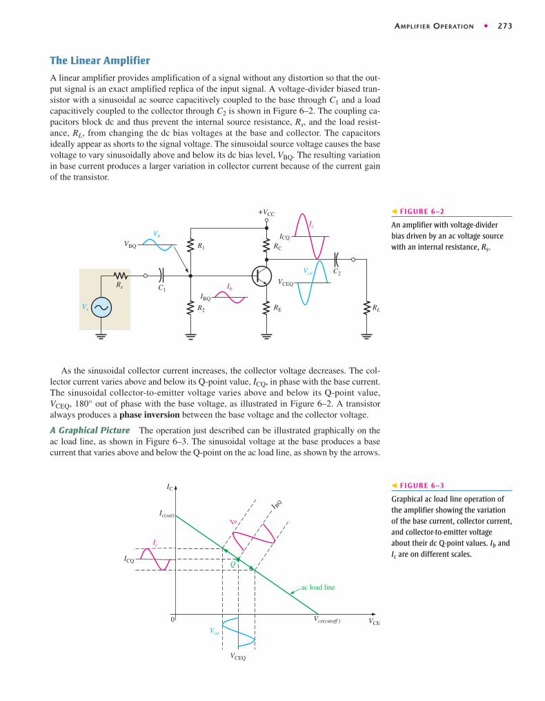
AMPLIFIER OPERATION ◆ 273
The Linear Amplifier
A linear amplifier provides amplification of a signal without any distortion so that the out-put signal is an exact amplified replica of the input signal. A voltage-divider biased tran-sistor with a sinusoidal ac source capacitively coupled to the base through C1 and a loadcapacitively coupled to the collector through C2 is shown in Figure 6–2. The coupling ca-pacitors block dc and thus prevent the internal source resistance, Rs, and the load resist-ance, RL, from changing the dc bias voltages at the base and collector. The capacitorsideally appear as shorts to the signal voltage. The sinusoidal source voltage causes the basevoltage to vary sinusoidally above and below its dc bias level, VBQ. The resulting variationin base current produces a larger variation in collector current because of the current gainof the transistor.
RC
+VCC
R1
RER2 RL
C2
Vb
IbRs
Ic
ICQ
Vce
VCEQ
Vs
C1IBQ
VBQ
� FIGURE 6–2
An amplifier with voltage-dividerbias driven by an ac voltage sourcewith an internal resistance, Rs.
As the sinusoidal collector current increases, the collector voltage decreases. The col-lector current varies above and below its Q-point value, ICQ, in phase with the base current.The sinusoidal collector-to-emitter voltage varies above and below its Q-point value,VCEQ, out of phase with the base voltage, as illustrated in Figure 6–2. A transistoralways produces a phase inversion between the base voltage and the collector voltage.
A Graphical Picture The operation just described can be illustrated graphically on theac load line, as shown in Figure 6–3. The sinusoidal voltage at the base produces a basecurrent that varies above and below the Q-point on the ac load line, as shown by the arrows.
180°
VCEQ
0 VCE
I b
IC
Ic
Q
ac load line
Vce
ICQ
Ic(sat)
Vce(cutoff )
I BQ
� FIGURE 6–3
Graphical ac load line operation ofthe amplifier showing the variationof the base current, collector current,and collector-to-emitter voltageabout their dc Q-point values. Ib andIc are on different scales.

274 ◆ BJT AMPLIFIERS
Lines projected from the peaks of the base current, across to the IC axis, and down to theVCE axis, indicate the peak-to-peak variations of the collector current and collector-to-emitter voltage, as shown. The ac load line differs from the dc load line because the effec-tive ac collector resistance is RL in parallel with RC and is less than the dc collector resist-ance RC alone. This difference between the dc and the ac load lines is covered in Chapter 7in relation to power amplifiers.
The ac load line operation of a certain amplifier extends above and below theQ-point base current value of as shown in Figure 6–4. Determine the resultingpeak-to-peak values of collector current and collector-to-emitter voltage from thegraph.
50 mA,10 mAEXAMPLE 6–1
Solution Projections on the graph of Figure 6–4 show the collector current varying from 6 mAto 4 mA for a peak-to-peak value of 2 mA and the collector-to-emitter voltage varyingfrom 1 V to 2 V for a peak-to-peak value of 1 V.
Related Problem* What are the Q-point values of IC and VCE in Figure 6–4?
1
2
3
1 2 3 40VCE (V)
10 A
20 A
30 A
40 A
50 A
70 A
IC (mA)
7
8
6
5
4
60 AIc
Vce
I b
Q
μ
μ
μ
μ
μ
μ
60 Aμ
50 Aμ
40 Aμ
μ
� FIGURE 6–4
*Answers can be found at www.pearsonhighered.com/floyd.
1. When Ib is at its positive peak, Ic is at its _____ peak, and Vce is at its _____ peak.
2. What is the difference between VCE and Vce?
3. What is the difference between Re and ?rœe
SECTION 6–1 CHECKUPAnswers can be found at www.pearsonhighered.com/floyd.

TRANSISTOR AC MODELS ◆ 275
r Parameters
The five r parameters commonly used for BJTs are given in Table 6–1. The italic lowercaseletter r with a prime denotes resistances internal to the transistor.
6–2 TRANSISTOR AC MODELS
To visualize the operation of a transistor in an amplifier circuit, it is often useful to represent the device by a model circuit. A transistor model circuit uses various internaltransistor parameters to represent its operation. Transistor models are described in thissection based on resistance or r parameters. Another system of parameters, called hparameters, is briefly described.
After completing this section, you should be able to
❏ Discuss transistor models❏ List and define the r parameters❏ Describe the r-parameter transistor model❏ Determine re� using a formula❏ Compare ac beta and dc beta❏ List and define the h parameters
� TABLE 6–1
r parameters.
r PARAMETER DESCRIPTION
ac alpha (Ic Ie)
ac beta (Ic Ib)
ac emitter resistance
ac base resistance
ac collector resistancer¿c
r¿b
r¿e
>bac
>aac
r-Parameter Transistor Model
An r-parameter model for a BJT is shown in Figure 6–5(a). For most general analysiswork, it can be simplified as follows: The effect of the ac base resistance is usuallysmall enough to neglect, so it can be replaced by a short. The ac collector resistance isusually several hundred kilohms and can be replaced by an open. The resulting simplifiedr-parameter equivalent circuit is shown in Figure 6–5(b).
The interpretation of this model circuit in terms of a transistor’s ac operation is asfollows: A resistance appears between the emitter and base terminals. This is theresistance “seen” looking into the emitter of a forward-biased transistor. The collectoreffectively acts as a dependent current source of or, equivalently, representedby the diamond-shaped symbol. These factors are shown with a transistor symbol inFigure 6–6.
Determining re� by a Formula
For amplifier analysis, the ac emitter resistance, is the most important of the r parame-ters. To calculate the approximate value of you can use Equation 6–1, which is derivedr¿e,
r¿e,
bacIb,aacIe
(r¿e)
(r¿c)(r ¿b)

276 ◆ BJT AMPLIFIERS
′rb
Ie
′rc�acIe
C
′re
Ib
B
E
(a) Generalized r-parameter model for a BJT
′re
B
(b) Simplified r-parameter model for a BJT
�acIe ≅ βacIb
C
E
� FIGURE 6–5
r-parameter transistor model.
assuming an abrupt junction between the n and p regions. It is also temperature dependentand is based on an ambient temperature of 20°C.
βacIb
C
B
E
Ic = βacIb
C
B
E
Ib ′re
′re
� FIGURE 6–6
Relation of transistor symbol to r-parameter model.
Equation 6–1
The numerator will be slightly larger for higher temperatures or transistors with a grad-ual (instead of an abrupt) junction. Although these cases will yield slightly differentresults, most designs are not critically dependent on the value of and you will gener-ally obtain excellent agreement with actual circuits using the equation as given. Thederivation for Equation 6–1 can be found in “Derivations of Selected Equations” atwww.pearsonhighered.com/floyd.
r¿e,
rœe �25 mV
IE
Determine the of a transistor that is operating with a dc emitter current of 2 mA.
Solution
Related Problem What is IE if r¿e = 8 Æ?
r¿e �25 mV
IE=
25 mV
2 mA= 12.5 æ
r¿eEXAMPLE 6–2

TRANSISTOR AC MODELS ◆ 277
Comparison of the AC Beta ( ac) to the DC Beta ( DC)
For a typical transistor, a graph of IC versus IB is nonlinear, as shown in Figure 6–7(a). Ifyou pick a Q-point on the curve and cause the base current to vary an amount then thecollector current will vary an amount as shown in part (b). At different points on thenonlinear curve, the ratio will be different, and it may also differ from the IC IBratio at the Q-point. Since the values of these two quan-tities can differ slightly.
bDC = IC>IB and bac = ¢IC>¢IB,>¢IC>¢IB
¢IC
¢IB,
BB
IBQ0
ICQ
IC
IB
Q
(a) βDC = IC/IB at Q-point
Q� IC
IC
IB
� IB
(IB,
IC)
0
(b) βac = � IC/� IB
� FIGURE 6–7
IC-versus-IB curve illustrates the dif-ference between Bac � ¢IC/¢IB.
BDC � IC/IB and
h Parameters
A manufacturer’s datasheet typically specifies h (hybrid) parameters (hi, hr, hf, and ho) be-cause they are relatively easy to measure.
The four basic ac h parameters and their descriptions are given in Table 6–2. Each of thefour h parameters carries a second subscript letter to designate the common-emitter (e),common-base (b), or common-collector (c) amplifier configuration, as listed in Table 6–3.The term common refers to one of the three terminals (E, B, or C) that is referenced to acground for both input and output signals. The characteristics of each of these three BJTamplifier configurations are covered later in this chapter.
� TABLE 6–2
Basic ac h parameters.h PARAMETER DESCRIPTION CONDITION
hi Input impedance (resistance) Output shorted
hr Voltage feedback ratio Input open
hf Forward current gain Output shorted
ho Output admittance (conductance) Input open
� TABLE 6–3
Subscripts of h parameters for each of the three amplifier configurations.
CONFIGURATION h PARAMETERS
Common-Emitter hie, hre, hfe, hoe
Common-Base hib, hrb, hfb, hob
Common-Collector hic, hrc, hfc, hoc
Relationships of h Parameters and r Parameters
The ac current ratios, convert directly from h parameters as follows:
bac = hfe
aac = hf b
aac and bac,

278 ◆ BJT AMPLIFIERS
Because datasheets often provide only common-emitter h parameters, the followingformulas show how to convert them to r parameters. We will use r parameters throughoutthe text because they are easier to apply and more practical.
r¿b = hie -hre
hoe(1 + hfe)
r¿c =hre + 1
hoe
r¿e =hre
hoe
1. Define each of the parameters:
2. Which h parameter is equivalent to
3. If IE � 15 mA, what is the approximate value of rœe?
Bac?
Aac, Bac, r¿e, r¿b, and r¿c.SECTION 6–2 CHECKUP
6–3 THE COMMON-EMIT TER AMPLIFIER
As you have learned, a BJT can be represented in an ac model circuit. Three amplifierconfigurations are the common-emitter, the common-base, and the common-collector.The common-emitter (CE) configuration has the emitter as the common terminal, orground, to an ac signal. CE amplifiers exhibit high voltage gain and high current gain.The common-collector and common-base configurations are covered in the sections6–4 and 6–5.
After completing this section, you should be able to
❏ Describe and analyze the operation of common-emitter amplifiers❏ Discuss a common-emitter amplifier with voltage-divider bias
◆ Show input and output signals ◆ Discuss phase inversion❏ Perform a dc analysis
◆ Represent the amplifier by its dc equivalent circuit❏ Perform an ac analysis
◆ Represent the amplifier by its ac equivalent circuit ◆ Define ac ground◆ Discuss the voltage at the base ◆ Discuss the input resistance at the base andthe output resistance
❏ Analyze the amplifier for voltage gain◆ Define attenuation ◆ Define bypass capacitor ◆ Describe the effect of an emitter bypass capacitor on voltage gain ◆ Discuss voltage gain without a bypass capacitor ◆ Explain the effect of a load on voltage gain
❏ Discuss the stability of the voltage gain◆ Define stability ◆ Explain the purpose of swamping re� and the effect on inputresistance
❏ Determine current gain and power gain
Figure 6–8 shows a common-emitter amplifier with voltage-divider bias and couplingcapacitors C1 and C3 on the input and output and a bypass capacitor, C2, from emitter toground. The input signal, Vin, is capacitively coupled to the base terminal, the output sig-nal, Vout, is capacitively coupled from the collector to the load. The amplified output is
out of phase with the input. Because the ac signal is applied to the base terminal as180°

THE COMMON-EMITTER AMPLIFIER ◆ 279
the input and taken from the collector terminal as the output, the emitter is common to boththe input and output signals. There is no signal at the emitter because the bypass capacitoreffectively shorts the emitter to ground at the signal frequency. All amplifiers have a com-bination of both ac and dc operation, which must be considered, but keep in mind that thecommon-emitter designation refers to the ac operation.
Phase Inversion The output signal is out of phase with the input signal. As theinput signal voltage changes, it causes the ac base current to change, resulting in a changein the collector current from its Q-point value. If the base current increases, the collectorcurrent increases above its Q-point value, causing an increase in the voltage drop acrossRC. This increase in the voltage across RC means that the voltage at the collector decreasesfrom its Q-point. So, any change in input signal voltage results in an opposite change incollector signal voltage, which is a phase inversion.
DC Analysis
To analyze the amplifier in Figure 6–8, the dc bias values must first be determined. To dothis, a dc equivalent circuit is developed by removing the coupling and bypass capacitorsbecause they appear open as far as the dc bias is concerned. This also removes the loadresistor and signal source. The dc equivalent circuit is shown in Figure 6–9.
Theveninizing the bias circuit and applying Kirchhoff’s voltage law to the base-emittercircuit,
VE = IERE = (3.58 mA)(560 Æ) = 2 V
IC � IE = 3.58 mA
IE =VTH - VBE
RE + RTH>bDC=
2.83 V - 0.7 V
560 Æ + 34.6 Æ= 3.58 mA
VTH = aR2
R1 + R2bVCC = a
6.8 kÆ6.8 kÆ + 22 kÆ
b 12 V = 2.83 V
RTH =R1R2
R1 + R2=
(6.8 kÆ)(22 kÆ)
6.8 kÆ + 22 kÆ= 5.19 kÆ
180°
R26.8
2.83 VDC
0
0
8.20 VDC
2.13 VDC
k� RE560 �
R122 k�
Vin
RC1.0 k�
VCC+12 V
VoutVout
βDC = 150
βac = 160
RL
C1
Vb
Vc
1 F
C210 F
C3
1 F
μ
μ
μ
� FIGURE 6–8
A common-emitter amplifier.
R122 k�
R26.8 k�
RE560 �
RC1.0 k�
VCC+12 V
βDC = 150
� FIGURE 6–9
DC equivalent circuit for the ampli-fier in Figure 6–8.

280 ◆ BJT AMPLIFIERS
AC Analysis
To analyze the ac signal operation of an amplifier, an ac equivalent circuit is developed asfollows:
1. The capacitors C1, C2, and C3 are replaced by effective shorts because their valuesare selected so that XC is negligible at the signal frequency and can be consideredto be
2. The dc source is replaced by ground.
A dc voltage source has an internal resistance of near because it holds a constant volt-age independent of the load (within limits); no ac voltage can be developed across it so itappears as an ac short. This is why a dc source is called an ac ground.
The ac equivalent circuit for the common-emitter amplifier in Figure 6–8 is shown inFigure 6–10(a). Notice that both RC and R1 have one end connected to ac ground (red) be-cause, in the actual circuit, they are connected to VCC which is, in effect, ac ground.
0 Æ
0 Æ.
VCE = VC - VE = 8.42 V - 2 V = 6.42 V
VC = VCC - ICRC = 12 V - (3.58 mA)(1.0 kÆ) = 8.42 V
VB = VE + 0.7 V = 2.7 V
RC1.0 k�
R122 k�
R26.8 k�
RC1.0 k�
R122 k�
R26.8 k�
Rs
Vs
(a) Without an input signal voltage (b) With an input signal voltage(AC ground is shown in red.)
ac source� FIGURE 6–10
AC equivalent circuit for the ampli-fier in Figure 6–8.
In ac analysis, the ac ground and the actual ground are treated as the same point electri-cally. The amplifier in Figure 6–8 is called a common-emitter amplifier because the bypasscapacitor C2 keeps the emitter at ac ground. Ground is the common point in the circuit.
Signal (AC) Voltage at the Base An ac voltage source, Vs, is shown connected to theinput in Figure 6–10(b). If the internal resistance of the ac source is then all of thesource voltage appears at the base terminal. If, however, the ac source has a nonzero inter-nal resistance, then three factors must be taken into account in determining the actual sig-nal voltage at the base. These are the source resistance (Rs), the bias resistanceand the ac input resistance at the base of the transistor This is illustrated inFigure 6–11(a) and is simplified by combining R1, R2, and Rin(base) in parallel to get thetotal input resistance, Rin(tot), which is the resistance “seen” by an ac source connected tothe input, as shown in Figure 6–11(b). A high value of input resistance is desirable so thatthe amplifier will not excessively load the signal source. This is opposite to the require-ment for a stable Q-point, which requires smaller resistors. The conflicting requirement forhigh input resistance and stable biasing is but one of the many trade-offs that must be con-sidered when choosing components for a circuit. The total input resistance is expressed bythe following formula:
(Rin(base)).(R1 7 R2),
0 Æ,
Equation 6–2 Rin(tot) � R1 7 R2 7 Rin(base)

THE COMMON-EMITTER AMPLIFIER ◆ 281
As you can see in the figure, the source voltage, Vs, is divided down by Rs (source resist-ance) and Rin(tot) so that the signal voltage at the base of the transistor is found by the volt-age-divider formula as follows:
If then where Vb is the input voltage, Vin, to the amplifier.
Input Resistance at the Base To develop an expression for the ac input resistance look-ing in at the base, use the simplified r-parameter model of the transistor. Figure 6–12shows the transistor model connected to the external collector resistor, RC. The inputresistance looking in at the base is
The base voltage is
and since
Substituting for Vb and Ib,
Cancelling Ie,
Rin(base) =Vb
Ib=
Ier¿eIe>bac
Ib �Ie
bac
Ie � Ic,
Vb = Ier¿e
Rin(base) =Vin
Iin=
Vb
Ib
Vb � VsRs V Rin(tot),
Vb = aRin(tot)
Rs + Rin(tot)bVs
R1
Rs
R2 Rin(base)
Base
Vs
(a)
Rs
Rin(tot) = R1 || R2 || Rin(base)
Base
Vs
(b)
Vin
� FIGURE 6–11
AC equivalent of the base circuit.
Vb
IbB
E
′re
Ie
βac Ib = Ic
C
+VCC
RC
� FIGURE 6–12
r-parameter transistor model (insideshaded block) connected to externalcircuit.
Equation 6–3
Output Resistance The output resistance of the common-emitter amplifier is the re-sistance looking in at the collector and is approximately equal to the collector resistor.
Rin(base) � Bacrœe
Equation 6–4
Actually, but since the internal ac collector resistance of the transistor, istypically much larger than RC, the approximation is usually valid.
r¿c,Rout = RC 7 r¿c,
Rout � RC
Determine the signal voltage at the base of the transistor in Figure 6–13. This circuit isthe ac equivalent of the amplifier in Figure 6–8 with a 10 mV rms, signalsource. IE was previously found to be 3.80 mA.
300 ÆEXAMPLE 6–3

282 ◆ BJT AMPLIFIERS
Voltage Gain
The ac voltage gain expression for the common-emitter amplifier is developed using themodel circuit in Figure 6–14. The gain is the ratio of ac output voltage at the collector (Vc)to ac input voltage at the base (Vb).
Notice in the figure that Therefore,
The Ie terms cancel, so
Av =IeRC
Ier¿e
Vc = aacIeRC � IeRC and Vb = Ier¿e.
Av =Vout
Vin=
Vc
Vb
Solution First, determine the ac emitter resistance.
Then,
Next, determine the total input resistance viewed from the source.
The source voltage is divided down by Rs and Rin(tot), so the signal voltage at thebase is the voltage across Rin(tot).
As you can see, there is significant attenuation (reduction) of the source voltage dueto the source resistance and amplifier’s input resistance combining to act as a voltagedivider.
Related Problem Determine the signal voltage at the base of Figure 6–13 if the source resistance is and another transistor with an ac beta of 200 is used.
75 Æ
Vb = aRin(tot)
Rs + Rin(tot)bVs = a
873 Æ1173 Æ
b10 mV = 7.44 mV
Rin(tot) = R1 7 R2 7 Rin(base) =1
1
22 kÆ+
1
6.8 kÆ+
1
1.05 kÆ
= 873 Æ
Rin(base) = bacr¿e = 160(6.58 Æ) = 1.05 kÆ
r¿e �25 mV
IE=
25 mV
3.80 mA= 6.58 Æ
R26.8 k�
RC1.0 k�R1
22 k�
Rs
300 �
Vs10 mV
βac = 160
� FIGURE 6–13
RC
r ′e
Vc
Vb
B
αacIe
E
C
Ie
� FIGURE 6–14
Model circuit for obtaining ac voltagegain.
Equation 6–5 Av �RC
r¿e

THE COMMON-EMITTER AMPLIFIER ◆ 283
Equation 6–5 is the voltage gain from base to collector. To get the overall gain of theamplifier from the source voltage to collector, the attenuation of the input circuit must beincluded.
Attenuation is the reduction in signal voltage as it passes through a circuit and corre-sponds to a gain of less than 1. For example, if the signal amplitude is reduced by half, theattenuation is 2, which can be expressed as a gain of 0.5 because gain is the reciprocal ofattenuation. Suppose a source produces a 10 mV input signal and the source resistancecombined with the load resistance results in a 2 mV output signal. In this case, the attenu-ation is 10 mV 2 mV � 5. That is, the input signal is reduced by a factor of 5. This can be>
R1 || R2
RC
AttenuationVs /Vb
Rs
Vs
Vb
Voltagegain
base-to-collector
Vc /Vb
Vout
Overallvoltage gain
Vc /Vs
Vc
� FIGURE 6–15
Base circuit attenuation and overall voltage gain.
Effect of the Emitter Bypass Capacitor on Voltage Gain The emitter bypass capac-itor, which is C2 in Figure 6–8, provides an effective short to the ac signal around theemitter resistor, thus keeping the emitter at ac ground, as you have seen. With the bypasscapacitor, the gain of a given amplifier is maximum and equal to
The value of the bypass capacitor must be large enough so that its reactance over thefrequency range of the amplifier is very small (ideally ) compared to RE. A goodrule-of-thumb is that the capacitive reactance, XC, of the bypass capacitor should be atleast 10 times smaller than RE at the minimum frequency for which the amplifier mustoperate.
10XC … RE
0 Æ
RC>r¿e.
expressed in terms of gain as 1 5 � 0.2.Assume that the amplifier in Figure 6–15 has a voltage gain from base to collector of Av
and the attenuation from the source to the base is Vs Vb. This attenuation is produced bythe source resistance and total input resistance of the amplifier acting as a voltage dividerand can be expressed as
The overall voltage gain of the amplifier, is the voltage gain from base to collector, Vc Vb,times the reciprocal of the attenuation, Vb Vs.
A¿v = aVc
Vbb a
Vb
Vsb =
Vc
Vs
>>A¿v,
Attenuation =Vs
Vb=
Rs + Rin(tot)
Rin(tot)
>
>

284 ◆ BJT AMPLIFIERS
Select a minimum value for the emitter bypass capacitor, C2, in Figure 6–16 if the amplifier must operate over a frequency range from 200 Hz to 10 kHz.
EXAMPLE 6–4
Calculate the base-to-collector voltage gain of the amplifier in Figure 6–16 both with-out and with an emitter bypass capacitor if there is no load resistor.
Solution From Example 6–3, for this same amplifier. Without C2, the gain is
Av =RC
r¿e + RE=
1.0 kÆ567 Æ
= 1.76
r¿e = 6.58 Æ
EXAMPLE 6–5
� FIGURE 6–16VCC
+12 V
RC1.0 k�
R26.8 k�
RE560 �
R122 k�
C1
C2
C3
2N3904
Vout
Vin
Solution The XC of the bypass capacitor, C2, should be at least ten times less than RE.
Determine the capacitance value at the minimum frequency of 200 Hz as follows:
This is the minimum value for the bypass capacitor for this circuit. You can always usea larger value, although cost and physical size may impose limitations.
Related Problem If the minimum frequency is reduced to 100 Hz, what value of bypass capacitor mustyou use?
C2 =1
2pf XC2=
1
2p(200 Hz)(56 Æ)= 14.2 MF
XC2 =RE
10=
560 Æ10
= 56 Æ
Voltage Gain Without the Bypass Capacitor To see how the bypass capacitor affectsac voltage gain, let’s remove it from the circuit in Figure 6–16 and compare voltage gains.
Without the bypass capacitor, the emitter is no longer at ac ground. Instead, RE is seenby the ac signal between the emitter and ground and effectively adds to in the voltagegain formula.
r¿e
Equation 6–6
The effect of RE is to decrease the ac voltage gain.
Av �RC
rœe � RE

THE COMMON-EMITTER AMPLIFIER ◆ 285
Effect of a Load on the Voltage Gain A load is the amount of current drawn from theoutput of an amplifier or other circuit through a load resistance. When a resistor, RL, is con-nected to the output through the coupling capacitor C3, as shown in Figure 6–17(a), it cre-ates a load on the circuit. The collector resistance at the signal frequency is effectively RCin parallel with RL. Remember, the upper end of RC is effectively at ac ground. The acequivalent circuit is shown in Figure 6–17(b). The total ac collector resistance is
Replacing RC with Rc in the voltage gain expression gives
Rc =RCRL
RC + RL
With C2, the gain is
As you can see, the bypass capacitor makes quite a difference.
Related Problem Determine the base-to-collector voltage gain in Figure 6–16 with RE bypassed, for thefollowing circuit values: RC = 1.8 kÆ, RE = 1.0 kÆ, R1 = 33 kÆ, and R2 = 6.8 kÆ.
Av =RC
r¿e=
1.0 kÆ6.58 Æ
= 152
Equation 6–7
When because of RL, the voltage gain is reduced. However, if thenand the load has very little effect on the gain.Rc � RC
RL W RC,Rc 6 RC
Av �Rc
rœe
Vin
+VCC
R1
C1
C2R2
RC
RE
RL
(a) Complete amplifier
R1 || R2
Rc = RC || RL
(b) AC equivalent (XC1 = XC2 = XC3 = 0)
Vout
C3
� FIGURE 6–17
A common-emitter amplifier with an ac (capacitively) coupled load.
Calculate the base-to-collector voltage gain of the amplifier in Figure 6–16 when aload resistance of is connected to the output. The emitter is effectively bypassedand
Solution The ac collector resistance is
Rc =RCRL
RC + RL=
(1.0 kÆ)(5 kÆ)
6 kÆ= 833 Æ
r¿e = 6.58 Æ.5 kÆ
EXAMPLE 6–6

286 ◆ BJT AMPLIFIERS
Stability of the Voltage Gain
Stability is a measure of how well an amplifier maintains its design values over changes intemperature or for a transistor with a different Although bypassing RE does produce themaximum voltage gain, there is a stability problem because the ac voltage gain is depend-ent on Also, depends on IE and on temperature. This causes thegain to be unstable over changes in temperature because when increases, the gain de-creases and vice versa.
With no bypass capacitor, the gain is decreased because RE is now in the ac circuitHowever, with RE unbypassed, the gain is much less dependent on
If the gain is essentially independent of because
Swamping r�e to Stabilize the Voltage Gain Swamping is a method used to minimizethe effect of without reducing the voltage gain to its minimum value. This method“swamps” out the effect of on the voltage gain. Swamping is, in effect, a compromisebetween having a bypass capacitor across RE and having no bypass capacitor at all.
In a swamped amplifier, RE is partially bypassed so that a reasonable gain can beachieved, and the effect of on the gain is greatly reduced or eliminated. The total external emitter resistance, RE, is formed with two separate emitter resistors, RE1 andRE2, as indicated in Figure 6–18. One of the resistors, RE2, is bypassed and the other is not.
Both resistors (RE1 � RE2) affect the dc bias while only RE1 affects the ac voltage gain.
Av =RC
r¿e + RE1
r¿e
r¿er¿e
Av �RC
RE
r¿eRE W r¿e,r¿e.(Av = RC>(r¿e + RE)).
r¿er¿er¿e since Av = RC>r¿e.
b.
Therefore,
The unloaded gain was found to be 152 in Example 6–5.
Related Problem Determine the base-to-collector voltage gain in Figure 6–16 when a load resist-ance is connected from collector to ground. Change the resistance values as follows:
and The emitter resistor iseffectively bypassed and r¿e = 18.5 Æ.
R2 = 6.8 kÆ.R1 = 33 kÆ,RE = 1.0 kÆ,RC = 1.8 kÆ,
10 kÆ
Av =Rc
r¿e=
833 Æ6.58 Æ
= 127
Vin
Vout
+VCC
R1
C3
C1
RC
R2
RE2
RE1
C2
� FIGURE 6–18
A swamped amplifier uses a partiallybypassed emitter resistance to mini-mize the effect of r�e on the gain inorder to achieve gain stability.

THE COMMON-EMITTER AMPLIFIER ◆ 287
If RE1 is at least ten times larger than then the effect of is minimized and theapproximate voltage gain for the swamped amplifier is
r¿er¿e,
Determine the voltage gain of the swamped amplifier in Figure 6–19. Assume that thebypass capacitor has a negligible reactance for the frequency at which the amplifier isoperated. Assume r¿e = 20 Æ.
EXAMPLE 6–7
Equation 6–8Av �RC
RE1
VCC+10 V
R133 k�
RC3.3 k�
RE2330 �
RE1330 �
C3
C1
R210 k�
1 F
Vin
Vout
C210 F
1 F
μ
μ
μ
� FIGURE 6–19
Solution RE2 is bypassed by C2. RE1 is more than ten times so the approximate voltage gain is
Related Problem What would be the voltage gain without C2? What would be the voltage gain with C2bypassing both RE1 and RE2?
Av �RC
RE1=
3.3 kÆ330 Æ
= 10
r¿e
The Effect of Swamping on the Amplifier’s Input Resistance The ac input resist-ance, looking in at the base of a common-emitter amplifier with RE completely bypassed,is When the emitter resistance is partially bypassed, the portion of the resist-ance that is unbypassed is seen by the ac signal and results in an increase in the ac inputresistance by appearing in series with The formula isr¿e.
Rin = bacr¿e.
Equation 6–9Rin(base) � Bac(rœe � RE1)
For the amplifier in Figure 6–20,
(a) Determine the dc collector voltage.
(b) Determine the ac collector voltage.
(c) Draw the total collector voltage waveform and the total output voltage waveform.
EXAMPLE 6–8
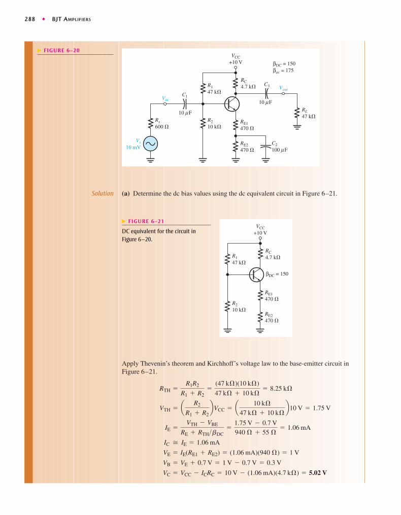
288 ◆ BJT AMPLIFIERS
Solution (a) Determine the dc bias values using the dc equivalent circuit in Figure 6–21.
10 Fμ
Vout
VCC+10 V
C3
Vs10 mV
RC4.7 k�
RL47 k�
R210 k�
RE2470 �
C2100 F
R147 k�
RE1470 �
Vin
Rs600 �
βDC = 150βac = 175
10 F
C1
μ
μ
� FIGURE 6–20
VCC+10 V
RC4.7 k�
R210 k�
RE2470 �
R147 k�
RE1470 �
βDC = 150
� FIGURE 6–21
DC equivalent for the circuit inFigure 6–20.
Apply Thevenin’s theorem and Kirchhoff’s voltage law to the base-emitter circuit inFigure 6–21.
VC = VCC - ICRC = 10 V - (1.06 mA)(4.7 kÆ) = 5.02 V
VB = VE + 0.7 V = 1 V - 0.7 V = 0.3 V
VE = IE(RE1 + RE2) = (1.06 mA)(940 Æ) = 1 V
IC � IE = 1.06 mA
IE =VTH - VBE
RE + RTH>bDC=
1.75 V - 0.7 V
940 Æ + 55 Æ= 1.06 mA
VTH = aR2
R1 + R2bVCC = a
10 kÆ47 kÆ + 10 kÆ
b10 V = 1.75 V
RTH =R1R2
R1 + R2=
(47 kÆ)(10 kÆ)
47 kÆ + 10 kÆ= 8.25 kÆ

THE COMMON-EMITTER AMPLIFIER ◆ 289
(b) The ac analysis is based on the ac equivalent circuit in Figure 6–22.
RE1470 �
R1 || R28.25 k�Vs
10 mV
βac = 175Vb
Rc =RCRL
RC + RL
Rs600 �
� FIGURE 6–22
AC equivalent for the circuit inFigure 6–20.
The first thing to do in the ac analysis is calculate
Next, determine the attenuation in the base circuit. Looking from the source, the total Rin is
Therefore,
The attenuation from source to base is
Before Av can be determined, you must know the ac collector resistance Rc.
The voltage gain from base to collector is
The overall voltage gain is the reciprocal of the attenuation times the amplifiervoltage gain.
The source produces 10 mV rms, so the rms voltage at the collector is
(c) The total collector voltage is the signal voltage of 84.5 mV rms riding on a dclevel of 4.74 V, as shown in Figure 6–23(a), where approximate peak values aredetermined as follows:
The coupling capacitor, C3, keeps the dc level from getting to the output. So, Vout is equalto the ac component of the collector voltage (Vout(p) � (84.5 mV)(1.414) � 119 mV),
Min Vc ( p) = VC - 1.414 Vc = 4.74 V - (84.5 mV)(1.414) = 4.62 V
Max Vc( p) = VC + 1.414 Vc = 4.74 V + (84.5 mV)(1.414) = 4.86 V
Vc = A¿vVs = (8.45)(10 mV) = 84.5 mV
A¿v = aVb
VsbAv = (0.93)(9.09) = 8.45
Av �Rc
RE1=
4.27 kÆ470 Æ
= 9.09
Rc =RCRL
RC + RL=
(4.7 kÆ)(47 kÆ)
4.7 kÆ + 47 kÆ= 4.27 kÆ
Attenuation =Vs
Vb=
Rs + Rin(tot)
Rin(tot)=
600 Æ + 7.53 kÆ7.53 kÆ
= 1.08
Rin(tot) = 47 kÆ 7 10 kÆ 7 86.5 kÆ = 7.53 kÆ
Rin(base) = bac(r¿e + RE1) = 175(494 Æ) = 86.5 kÆ Rin(tot) = R1 7 R2 7 Rin(base)
600 Æ
r¿e �25 mV
IE=
25 mV
1.06 mA= 23.6 Æ
r¿e.

290 ◆ BJT AMPLIFIERS
Current Gain
The current gain from base to collector is However, the overall current gain ofthe common-emitter amplifier is
Ic>Ib or bac.
as indicated in Figure 6–23(b). The source voltage, Vs, is shown to emphasize thephase inversion.
Related Problem What is Av in Figure 6–20 with RL removed?
Open the Multisim file E06-08 in the Examples folder on the companion website.Measure the dc and the ac values of the collector voltage and compare with the calculated values.
(a) Total collector voltage
+119 mV
0 V
–119 mV
(b) Source and output ac voltages
Vout
Vs
4.86 V
4.74 V
4.62 V
Vc
� FIGURE 6–23
Voltages for Figure 6–20.
Equation 6–10
Is is the total signal input current produced by the source, part of which (Ib) is base cur-rent and part of which (Ibias) goes through the bias circuit as shown in Figure6–24. The source “sees” a total resistance of The total current produced bythe source is
Is =Vs
Rs + Rin(tot)
Rs + Rin(tot).(R1 7 R2),
Ai �Ic
Is
R1 || R2
Rc
Ibias
Is
Rs
Vs
+
–
Ib Ic
Rin(tot)
Vb
Vc� FIGURE 6–24
Signal currents (directions shown arefor the positive half-cycle of Vs ).

THE COMMON-COLLECTOR AMPLIFIER ◆ 291
Power Gain
The overall power gain is the product of the overall voltage gain and the overall cur-rent gain (Ai).
(A¿v)
Equation 6–11
where A¿v = Vc>Vs.
Ap � A¿v Ai
1. In the dc equivalent circuit of an amplifier, how are the capacitors treated?
2. When the emitter resistor is bypassed with a capacitor, how is the gain of the amplifieraffected?
3. Explain swamping.
4. List the elements included in the total input resistance of a common-emitteramplifier.
5. What elements determine the overall voltage gain of a common-emitter amplifier?
6. When a load resistor is capacitively coupled to the collector of a CE amplifier, is thevoltage gain increased or decreased?
7. What is the phase relationship of the input and output voltages of a CE amplifier?
SECTION 6–3 CHECKUP
6–4 THE COMMON-COLLECTOR AMPLIFIER
The common-collector (CC) amplifier is usually referred to as an emitter-follower(EF). The input is applied to the base through a coupling capacitor, and the output is atthe emitter. The voltage gain of a CC amplifier is approximately 1, and its main advan-tages are its high input resistance and current gain.
After completing this section, you should be able to
❏ Describe and analyze the operation of common-collector amplifiers❏ Discuss the emitter-follower amplifier with voltage-divider bias❏ Analyze the amplifier for voltage gain
◆ Explain the term emitter-follower❏ Discuss and calculate input resistance❏ Determine output resistance❏ Determine current gain❏ Determine power gain❏ Describe the Darlington pair
◆ Discuss an application❏ Discuss the Sziklai pair
An emitter-follower circuit with voltage-divider bias is shown in Figure 6–25. Noticethat the input signal is capacitively coupled to the base, the output signal is capacitivelycoupled from the emitter, and the collector is at ac ground. There is no phase inversion, andthe output is approximately the same amplitude as the input.
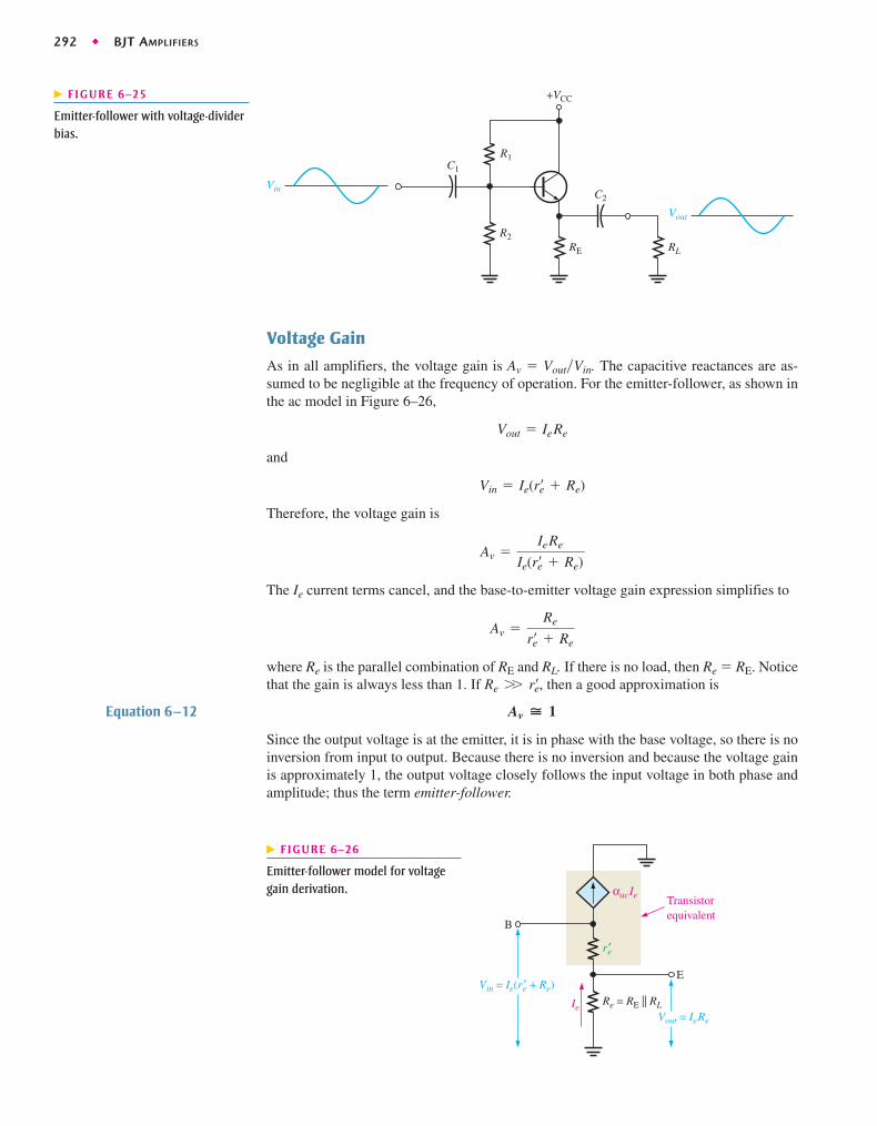
292 ◆ BJT AMPLIFIERS
Voltage Gain
As in all amplifiers, the voltage gain is Av � Vout�Vin. The capacitive reactances are as-sumed to be negligible at the frequency of operation. For the emitter-follower, as shown inthe ac model in Figure 6–26,
and
Therefore, the voltage gain is
The Ie current terms cancel, and the base-to-emitter voltage gain expression simplifies to
where Re is the parallel combination of RE and RL. If there is no load, then Re � RE. Noticethat the gain is always less than 1. If then a good approximation isRe W r¿e,
Av =Re
r¿e + Re
Av =IeRe
Ie(r¿e + Re)
Vin = Ie(r¿e + Re)
Vout = IeRe
+VCC
R1
R2RE RL
Vin
Vout
C1
C2
� FIGURE 6–25
Emitter-follower with voltage-dividerbias.
Equation 6–12
Since the output voltage is at the emitter, it is in phase with the base voltage, so there is noinversion from input to output. Because there is no inversion and because the voltage gainis approximately 1, the output voltage closely follows the input voltage in both phase andamplitude; thus the term emitter-follower.
Av � 1
r ′e
Vin = Ie(r ′e + Re)
B
αacIe
E
Vout = IeRe
Re = RE || RLIe
Transistorequivalent
� FIGURE 6–26
Emitter-follower model for voltagegain derivation.

THE COMMON-COLLECTOR AMPLIFIER ◆ 293
Input Resistance
The emitter-follower is characterized by a high input resistance; this is what makes it auseful circuit. Because of the high input resistance, it can be used as a buffer to minimizeloading effects when a circuit is driving a low-resistance load. The derivation of the inputresistance, looking in at the base of the common-collector amplifier, is similar to that forthe common-emitter amplifier. In a common-collector circuit, however, the emitter resistoris never bypassed because the output is taken across Re, which is RE in parallel with RL.
Since
The Ib terms cancel; therefore,
If then the input resistance at the base is simplified toRe W r¿e,
Rin(base) � bac(r¿e + Re)
Rin(base) �bacIb(r¿e + Re)
Ib
Ie � Ic = bacIb,
Rin(base) =Vin
Iin=
Vb
Ib=
Ie(r¿e + Re)
Ib
Equation 6–13
Equation 6–14
Equation 6–15
Equation 6–16
The bias resistors in Figure 6–25 appear in parallel with Rin(base), looking from the inputsource; and just as in the common-emitter circuit, the total input resistance is
Output Resistance
With the load removed, the output resistance, looking into the emitter of the emitter-follower,is approximated as follows:
Rin(tot) = R1 7 R2 7 Rin(base)
Rin(base) � BacRe
where
Power Gain
The common-collector power gain is the product of the voltage gain and the current gain.For the emitter-follower, the power gain is approximately equal to the current gain becausethe voltage gain is approximately 1.
Since the power gain isAv � 1,
Ap = Av Ai
Iin = Vin>Rin(tot).
Ai �Ie
Iin
Ap � Ai
Rs is the resistance of the input source. The derivation of Equation 6–14, found in“Derivations of Selected Equations” at www.pearsonhighered.com/floyd, is relativelyinvolved and several assumptions have been made. The output resistance is very low, makingthe emitter-follower useful for driving low-resistance loads.
Current Gain
The current gain for the emitter-follower in Figure 6–25 is
Rout � aRs
Bacb 7 RE

294 ◆ BJT AMPLIFIERS
Determine the total input resistance of the emitter-follower in Figure 6–27. Also findthe voltage gain, current gain, and power gain in terms of power delivered to the load,RL. Assume and that the capacitive reactances are negligible at the fre-quency of operation.
bac = 175
EXAMPLE 6–9
Solution The ac emitter resistance external to the transistor is
The approximate resistance, looking in at the base, is
The total input resistance is
The voltage gain is By using you can determine a more precise value ofAv if necessary.
Therefore,
and
So,
The small difference in Av as a result of considering is insignificant in most cases.The current gain is The calculations are as follows:
Ai =Ie
Iin=
12.7 mA
297 mA= 42.8
Iin =Vin
Rin(tot)=
3 V
10.1 kÆ= 297 mA
Ie =Ve
Re=
AvVb
Re�
(0.992)(3 V)
235 Æ=
2.98 V
235 Æ= 12.7 mA
Ai = Ie>Iin.r¿e
Av =Re
r¿e + Re=
235 Æ237 Æ
= 0.992
r¿e �25 mV
IE=
25 mV
14.2 mA= 1.76 Æ
IE =VE
RE=
6.69 V
470 Æ= 14.2 mA
= (0.739)(10 V) - 0.7 V = 6.69 V
VE = aR2
R1 + R2bVCC - VBE = a
51 kÆ18 kÆ + 51 kÆ
b10 V - 0.7 V
r¿e,Av � 1.
Rin(tot) = R1 7 R2 7 Rin(base) = 18 kÆ 7 51 kÆ 7 41.1 kÆ = 10.1 kæ
Rin(base) � bacRe = (175)(235 Æ) = 41.1 kÆ
Re = RE 7 RL = 470 Æ 7 470 Æ = 235 Æ
VCC+10 V
R118 k�
R251 k� RE
470 �
Vout
RL470 �
Vin
3 V rms
C1
C2
2N3904
10 Fμ
1 Fμ
� FIGURE 6–27

THE COMMON-COLLECTOR AMPLIFIER ◆ 295
The Darlington Pair
As you have seen, is a major factor in determining the input resistance of an amplifier.The of the transistor limits the maximum achievable input resistance you can get froma given emitter-follower circuit.
One way to boost input resistance is to use a Darlington pair, as shown in Figure 6–28.The collectors of two transistors are connected, and the emitter of the first drives the baseof the second. This configuration achieves multiplication as shown in the followingsteps. The emitter current of the first transistor is
This emitter current becomes the base current for the second transistor, producing a sec-ond emitter current of
Therefore, the effective current gain of the Darlington pair is
Neglecting by assuming that it is much smaller than RE, the input resistance isre¿
bac = bac1bac2
Ie2 � bac2Ie1 = bac1bac2Ib1
Ie1 � bac1Ib1
bac
bac
bac
The power gain is
Since RL � RE, one-half of the power is dissipated in RE and one-half in RL. Therefore,in terms of power to the load, the power gain is
Related Problem If RL in Figure 6–27 is decreased in value, does power gain to the load increase ordecrease?
Open the Multisim file E06-09 in the Examples folder on the companion website.Measure the voltage gain and compare with the calculated value.
Ap(load ) =Ap
2=
42.8
2= 21.4
Ap � Ai = 42.8
Sidney Darlington (1906–1997) wasa renowned electrical engineer,whose name lives on through thetransistor configuration he patentedin 1953. He also had inventions inchirp radar, bombsights, and gunand rocket guidance. In 1945, hewas awarded the Presidential Medalof Freedom and in 1975, he receivedIEEE’s Edison Medal “for basiccontributions to network theory andfor important inventions in radarsystems and electronic circuits” andthe IEEE Medal of Honor in 1981“for fundamental contributions tofiltering and signal processingleading to chirp radar.”
H I S T O R Y N O T E
Equation 6–17Rin � Bac1Bac2RE
+VCC
RE
βac1
βac2
Ie2 ≅ βac1βac2Ib1
Ie1 ≅ βac1Ib1
Ib1
Vin
� FIGURE 6–28
A Darlington pair multiplies �ac.
An Application The emitter-follower is often used as an interface between a circuit witha high output resistance and a low-resistance load. In such an application, the emitter-follower is called a buffer.
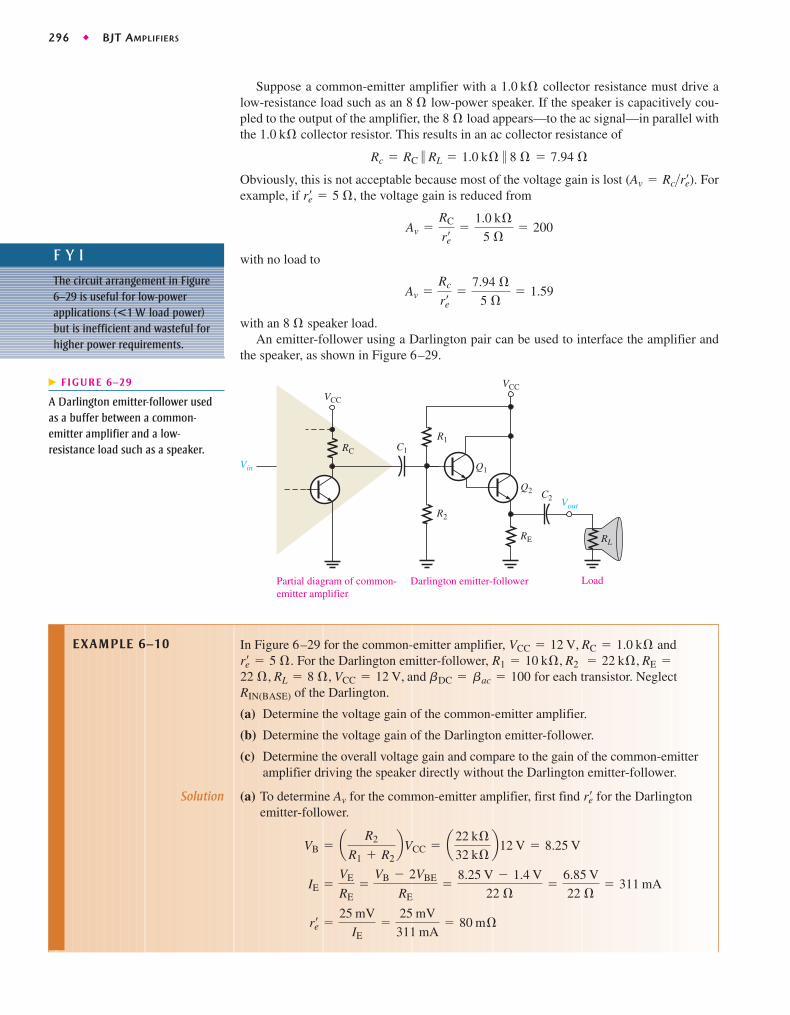
296 ◆ BJT AMPLIFIERS
Suppose a common-emitter amplifier with a collector resistance must drive alow-resistance load such as an low-power speaker. If the speaker is capacitively cou-pled to the output of the amplifier, the load appears—to the ac signal—in parallel withthe collector resistor. This results in an ac collector resistance of
Obviously, this is not acceptable because most of the voltage gain is lost Forexample, if the voltage gain is reduced from
with no load to
with an speaker load.An emitter-follower using a Darlington pair can be used to interface the amplifier and
the speaker, as shown in Figure 6–29.
8 Æ
Av =Rc
r¿e=
7.94 Æ5 Æ
= 1.59
Av =RC
r¿e=
1.0 kÆ5 Æ
= 200
r¿e = 5 Æ,(Av = Rc>r¿e).
Rc = RC 7 RL = 1.0 kÆ 7 8 Æ = 7.94 Æ
1.0 kÆ8 Æ
8 Æ1.0 kÆ
The circuit arrangement in Figure6–29 is useful for low-powerapplications load power)but is inefficient and wasteful forhigher power requirements.
(<1 W
F Y I
VCC
R1
C2
R2
RE RL
Vin
LoadDarlington emitter-followerPartial diagram of common-emitter amplifier
Q2
Q1
VCC
RC C1
Vout
� FIGURE 6–29
A Darlington emitter-follower usedas a buffer between a common-emitter amplifier and a low-resistance load such as a speaker.
In Figure 6–29 for the common-emitter amplifier, andFor the Darlington emitter-follower,
for each transistor. Neglectof the Darlington.
(a) Determine the voltage gain of the common-emitter amplifier.
(b) Determine the voltage gain of the Darlington emitter-follower.
(c) Determine the overall voltage gain and compare to the gain of the common-emitteramplifier driving the speaker directly without the Darlington emitter-follower.
Solution (a) To determine Av for the common-emitter amplifier, first find for the Darlingtonemitter-follower.
r¿e =25 mV
IE=
25 mV
311 mA= 80 mÆ
IE =VE
RE=
VB - 2VBE
RE=
8.25 V - 1.4 V
22 Æ=
6.85 V
22 Æ= 311 mA
VB = aR2
R1 + R2bVCC = a
22 kÆ32 kÆ
b12 V = 8.25 V
r¿e
RIN(BASE)
bac = 10022 Æ, RL = 8 Æ, VCC = 12 V, and bDC == 22 kÆ, RE =R1 = 10 kÆ, R2r¿e = 5 Æ.
VCC = 12 V, RC = 1.0 kÆEXAMPLE 6–10

THE COMMON-COLLECTOR AMPLIFIER ◆ 297
The Sziklai Pair
The Sziklai pair, shown in Figure 6–30, is similar to the Darlington pair except that itconsists of two types of transistors, an npn and a pnp. This configuration is sometimes
Note that RE must dissipate a power of
and transistor Q2 must dissipate
Next, the ac emitter resistance of the Darlington emitter-follower is
The total input resistance of the Darlington emitter-follower is
The effective ac collector resistance of the common-emitter amplifier is
The voltage gain of the common-emitter amplifier is
(b) The effective ac emitter resistance was found in part (a) to be The voltagegain for the Darlington emitter-follower is
(c) The overall voltage gain is
If the common-emitter amplifier drives the speaker directly, the gain is 1.59 as wepreviously calculated.
Related Problem Using the same circuit values, determine the voltage gain of the common-emitteramplifier in Figure 6–29 if a single transistor is used in the emitter-follower in place ofthe Darlington pair. Assume Explain the difference in the voltagegain without the Darlington pair.
bDC = bac = 100.
A¿v = Av (EF) Av (CE) = (0.99)(172) = 170
Av =Re
r¿e + Re=
5.87 Æ80 mÆ + 5.87 Æ
= 0.99
5.87 Æ.
Av =Rc
r¿e=
860 Æ5 Æ
= 172
Rc = RC 7 Rin(tot) = 1.0 kÆ 7 6.16 kÆ = 860 Æ
= 10 kÆ 7 22 kÆ 7 1002(80 mÆ + 5.87 Æ) = 6.16 kÆ Rin(tot) = R1 7 R2 7 b2
ac (r¿e + Re)
Re = RE 7 RL = 22 Æ 7 8 Æ = 5.87 Æ
PQ2 = (VCC - VE)IE = (5.4 V)(311 mA) = 1.68 W
PRE= I2
ERE = (311 mA)2(22 Æ) = 2.13 W
George Clifford Sziklai, born inHungary in 1909, was an electronicsengineer, who emigrated to NewYork in 1930. Among many othercontributions to radio and TV, heinvented the transistorconfiguration named after him, theSziklai pair, also known as thecomplementary Darlington. Sziklaiis also credited with constructingthe first image orthicon televisioncamera and inventing a high-speedelevator in addition to some 200other patents.
H I S T O R Y N O T E
+VCC
RE
Q2
Q1
βac1Ib
βac1βac2Ib
βac1Ib
Ib
� FIGURE 6–30
The Sziklai pair.

298 ◆ BJT AMPLIFIERS
known as a complementary Darlington or a compound transistor. The current gain isabout the same as in the Darlington pair, as illustrated. The difference is that the Q2 basecurrent is the Q1 collector current instead of emitter current, as in the Darlingtonarrangement.
An advantage of the Sziklai pair, compared to the Darlington, is that it takes lessvoltage to turn it on because only one barrier potential has to be overcome. A Sziklaipair is sometimes used in conjunction with a Darlington pair as the output stage ofpower amplifiers. In this case, the output power transistors are both the same type (twonpn or two pnp transistors). This makes it easier to obtain exact matches of the outputtransistors, resulting in improved thermal stability and better sound quality in audioapplications.
1. What is a common-collector amplifier called?
2. What is the ideal maximum voltage gain of a common-collector amplifier?
3. What characteristic of the common-collector amplifier makes it a useful circuit?
SECTION 6–4 CHECKUP
6–5 THE COMMON-BASE AMPLIFIER
The common-base (CB) amplifier provides high voltage gain with a maximumcurrent gain of 1. Since it has a low input resistance, the CB amplifier is the most appro-priate type for certain applications where sources tend to have very low-resistanceoutputs.
After completing this section, you should be able to
❏ Describe and analyze the operation of common-base amplifiers❏ Determine the voltage gain
◆ Explain why there is no phase inversion❏ Discuss and calculate input resistance❏ Determine output resistance❏ Determine current gain❏ Determine power gain
A typical common-base amplifier is shown in Figure 6–31. The base is the commonterminal and is at ac ground because of capacitor C2. The input signal is capacitivelycoupled to the emitter. The output is capacitively coupled from the collector to a loadresistor.
Voltage Gain
The voltage gain from emitter to collector is developed as follows
Av =Vout
Vin=
Vc
Ve=
Ic Rc
Ie(r¿e 7 RE)�
Ie Rc
Ie(r¿e 7 RE)
(Vin = Ve, Vout = Vc).
The CB amplifier is useful at highfrequencies when impedancematching is required because inputimpedance can be controlled andbecause noninverting amps havebetter frequency response.
F Y I

THE COMMON-BASE AMPLIFIER ◆ 299
+VCC
C3RC
RL
R2 RE
R1
C1
Vin
Rc = RC || RL
RE
r ′e
E
B
(a) Complete circuit with load (b) AC equivalent model
IcC2
Vin
Vout
� FIGURE 6–31
Common-base amplifier with voltage-divider bias.
Equation 6–18
Equation 6–19
Equation 6–20
Equation 6–21
Equation 6–22
where Notice that the gain expression is the same as for the common-emitteramplifier. However, there is no phase inversion from emitter to collector.
Input Resistance
The resistance, looking in at the emitter, is
If thenRE W r¿e,
Rin(emitter) =Vin
Iin=
Ve
Ie=
Ie(r¿e 7 RE)
Ie
Rc = RC 7 RL.
Av �Rc
r¿e
RE is typically much greater than so the assumption that is usually valid.The input resistance can be set to a desired value by using a swamping resistor.
Output Resistance
Looking into the collector, the ac collector resistance, appears in parallel with RC. Asyou have previously seen in connection with the CE amplifier, is typically much largerthan RC, so a good approximation for the output resistance is
r¿cr¿c,
r¿e 7 RE � r¿er¿e,
Rin(emitter) � r¿e
Current Gain
The current gain is the output current divided by the input current. Ic is the ac output cur-rent, and Ie is the ac input current. Since the current gain is approximately 1.Ic � Ie,
Rout � RC
Power Gain
Since the current gain is approximately 1 for the common-base amplifier and the power gain is approximately equal to the voltage gain.
Ap = Av Ai,
Ai � 1
AP � Av
If thenRE W r¿e,
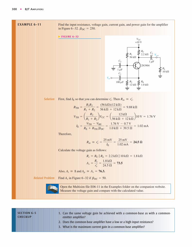
300 ◆ BJT AMPLIFIERS
Find the input resistance, voltage gain, current gain, and power gain for the amplifierin Figure 6–32. bDC = 250.
EXAMPLE 6–11
Vout
VCC+10 V
Vin
RL10 k�
RC2.2 k�
R212 k�
RE1.0 k�
R156 k�
2N3904
C2
C1
100 F
C3
1 Fμ
1 Fμ
μ
� FIGURE 6–32
Solution First, find IE so that you can determine Then
Therefore,
Calculate the voltage gain as follows:
Also,
Related Problem Find Av in Figure 6–32 if
Open the Multisim file E06-11 in the Examples folder on the companion website.Measure the voltage gain and compare with the calculated value.
bDC = 50.
Ai � 1 and Ap � Av = 76.3.
Av =Rc
r¿e=
1.8 kÆ24.5 Æ
= 73.5
Rc = RC 7 RL = 2.2 kÆ 7 10 kÆ = 1.8 kÆ
Rin � r¿e =25 mV
IE=
25 mV
1.02 mA= 24.5 æ
IE =VTH - VBE
RE + RTH>bDC=
1.76 V - 0.7 V
1.0 kÆ + 39.5 Æ= 1.02 mA
VTH = aR2
R1 + R2bVCC = a
12 kÆ56 kÆ + 12 kÆ
b10 V = 1.76 V
RTH =R1R2
R1 + R2=
(56 kÆ)(12 kÆ)
56 kÆ + 12 kÆ= 9.88 kÆ
Rin � r¿e.r¿e.
1. Can the same voltage gain be achieved with a common-base as with a common-emitter amplifier?
2. Does the common-base amplifier have a low or a high input resistance?
3. What is the maximum current gain in a common-base amplifier?
SECTION 6–5 CHECKUP

MULTISTAGE AMPLIFIERS ◆ 301
Multistage Voltage Gain
The overall voltage gain, of cascaded amplifiers, as shown in Figure 6–33, is the productof the individual voltage gains.
A¿v,
6–6 MULTISTAGE AMPLIFIERS
Two or more amplifiers can be connected in a cascaded arrangement with the outputof one amplifier driving the input of the next. Each amplifier in a cascaded arrange-ment is known as a stage. The basic purpose of a multistage arrangement is to increasethe overall voltage gain. Although discrete multistage amplifiers are not as common asthey once were, a familiarization with this area provides insight into how circuitsaffect each other when they are connected together.
After completing this section, you should be able to
❏ Describe and analyze the operation of multistage amplifiers❏ Determine the overall voltage gain of multistage amplifiers
◆ Express the voltage gain in decibels (dB)❏ Discuss and analyze capacitively-coupled multistage amplifiers
◆ Describe loading effects ◆ Determine the voltage gain of each stage in a two-stage amplifier ◆ Determine the overall voltage gain ◆ Determine the dc voltages
❏ Describe direct-coupled multistage amplifiers
Equation 6–23
where n is the number of stages.
A¿v � Av1Av2Av3 Á Avn
Equation 6–24
Amplifier voltage gain is often expressed in decibels (dB) as follows:
This is particularly useful in multistage systems because the overall voltage gain in dB isthe sum of the individual voltage gains in dB.
A¿v(dB) = Av1(dB) + Av2(dB) + Á + Avn(dB)
Av(dB) � 20 log Av
Av3Av2Av1 AvnInput
VCC
Output
� FIGURE 6–33
Cascaded amplifiers. Each triangular symbol represents a separate amplifier.
A certain cascaded amplifier arrangement has the following voltage gains: What is the overall voltage gain? Also express each gain in
decibels (dB) and determine the total voltage gain in dB.Av2 = 15, and Av3 = 20.
Av1 = 10, EXAMPLE 6–12

302 ◆ BJT AMPLIFIERS
Capacitively-Coupled Multistage Amplifier
For purposes of illustration, we will use the two-stage capacitively coupled amplifier inFigure 6–34. Notice that both stages are identical common-emitter amplifiers with theoutput of the first stage capacitively coupled to the input of the second stage. Capacitivecoupling prevents the dc bias of one stage from affecting that of the other but allows the acsignal to pass without attenuation because at the frequency of operation.Notice, also, that the transistors are labeled Q1 and Q2.
XC � 0 Æ
1 Fμ
1 Fμ
VCC+10 V
βDC = βac = 150 for Q1 and Q2
R74.7 k�
R81.0 k�
R610 k�
Vout
R34.7 k�
R41.0 k�
R210 k�
Q1Vin Q2
C5
R547 k�
R147 k�
1st stage 2nd stage
C4100 F
1 F
C3C1
C2100 F
μ
μ μ
� FIGURE 6–34
A two-stage common-emitter amplifier.
Solution
Related Problem In a certain multistage amplifier, the individual stages have the following voltagegains: What is the overall gain? Express each gainin dB and determine the total voltage gain in dB.
Av1 = 25, Av2 = 5, and Av3 = 12.
A¿v(dB) = 20.0 dB + 23.5 dB + 26.0 dB = 69.5 dB
Av3(dB) = 20 log 20 = 26.0 dB
Av2(dB) = 20 log 15 = 23.5 dB
Av1(dB) = 20 log 10 = 20.0 dB
A¿v = Av1Av2Av3 = (10)(15)(20) = 3000
Loading Effects In determining the voltage gain of the first stage, you must consider theloading effect of the second stage. Because the coupling capacitor C3 effectively appearsas a short at the signal frequency, the total input resistance of the second stage presents anac load to the first stage.
Looking from the collector of Q1, the two biasing resistors in the second stage, R5and R6, appear in parallel with the input resistance at the base of Q2. In other words, thesignal at the collector of Q1 “sees” R3, R5, R6, and Rin(base2) of the second stage all inparallel to ac ground. Thus, the effective ac collector resistance of Q1 is the total of allthese resistances in parallel, as Figure 6–35 illustrates. The voltage gain of the firststage is reduced by the loading of the second stage because the effective ac collectorresistance of the first stage is less than the actual value of its collector resistor, R3.Remember that Av = Rc>r¿e.

MULTISTAGE AMPLIFIERS ◆ 303
Voltage Gain of the First Stage The ac collector resistance of the first stage is
Remember that lowercase italic subscripts denote ac quantities such as for Rc.You can verify that IE 1.05 mA, , and The effective
ac collector resistance of the first stage is as follows:
Therefore, the base-to-collector voltage gain of the first stage is
Voltage Gain of the Second Stage The second stage has no load resistor, so the ac col-lector resistance is R7, and the gain is
Compare this to the gain of the first stage, and notice how much the loading from the sec-ond stage reduced the gain.
Overall Voltage Gain The overall amplifier gain with no load on the output is
If an input signal of , for example, is applied to the first stage and if there is no atten-uation in the input base circuit due to the source resistance, an output from the second stageof will result. The overall voltage gain can be expressed in dBas follows:
DC Voltages in the Capacitively Coupled Multistage Amplifier Since both stages inFigure 6–34 are identical, the dc voltages for Q1 and Q2 are the same. Since and the dc base voltage for Q1 and Q2 is
The dc emitter and collector voltages are as follows:
VC = VCC - ICR3 = 10 V - (1.05 mA)(4.7 kÆ) = 5.07 V
IC � IE = 1.05 mA
IE =VE
R4=
1.05 V
1.0 kÆ= 1.05 mA
VE = VB - 0.7 V = 1.05 V
VB � aR2
R1 + R2bVCC = a
10 kÆ57 kÆ
b10 V = 1.75 V
bDCR8 W R6,bDCR4 W R2
A¿v(dB) = 20 log (13,495) = 82.6 dB
(100 mV)(13,495) � 1.35 V
100 mV
A¿v = Av1Av2 = (68.5)(197) � 13,495
Av2 =R7
r¿e=
4.7 kÆ23.8 Æ
= 197
Av1 =Rc1
r¿e=
1.63 kÆ23.8 Æ
= 68.5
Rc1 = 4.7 kÆ 7 47 kÆ 7 10 kÆ 7 3.57 kÆ = 1.63 kÆ
Rin(base2) = 3.57 kÆ.r¿e = 23.8Æ=
Rc1 = R3 7 R5 7 R6 7 Rin(base2)
Vin Q1
R34.7 k�
R547 k�
R610 k�
Rin(base 2)3.57 k�
Input resistance of second stage � FIGURE 6–35
AC equivalent of first stage in Figure6–34, showing loading from secondstage input resistance.

304 ◆ BJT AMPLIFIERS
Direct-Coupled Multistage Amplifiers
A basic two-stage, direct-coupled amplifier is shown in Figure 6–36. Notice that there areno coupling or bypass capacitors in this circuit. The dc collector voltage of the first stageprovides the base-bias voltage for the second stage. Because of the direct coupling, thistype of amplifier has a better low-frequency response than the capacitively coupled type inwhich the reactance of coupling and bypass capacitors at very low frequencies may be-come excessive. The increased reactance of capacitors at lower frequencies produces gainreduction in capacitively coupled amplifiers.
Direct-coupled amplifiers can be used to amplify low frequencies all the way down to dc(0 Hz) without loss of voltage gain because there are no capacitive reactances in the circuit.The disadvantage of direct-coupled amplifiers, on the other hand, is that small changes in thedc bias voltages from temperature effects or power-supply variation are amplified by the suc-ceeding stages, which can result in a significant drift in the dc levels throughout the circuit.
Vout
Q1Vin Q2
R5
R6
R3
R4R2
R1
+VCC� FIGURE 6–36
A basic two-stage direct-coupled amplifier.
1. What does the term stage mean?
2. How is the overall voltage gain of a multistage amplifier determined?
3. Express a voltage gain of 500 in dB.
4. Discuss a disadvantage of a capacitively coupled amplifier.
SECTION 6–6 CHECKUP
6–7 THE DIFFERENTIAL AMPLIFIER
A differential amplifier is an amplifier that produces outputs that are a function of thedifference between two input voltages. The differential amplifier has two basic modes ofoperation: differential (in which the two inputs are different) and common mode (inwhich the two inputs are the same). The differential amplifier is important in operationalamplifiers, which are covered beginning in Chapter 12.
After completing this section, you should be able to
❏ Describe the differential amplifier and its operation❏ Discuss the basic operation
◆ Calculate dc currents and voltages❏ Discuss the modes of signal operation
◆ Describe single-ended differential input operation ◆ Describe double-endeddifferential input operation ◆ Determine common-mode operation
❏ Define and determine the common-mode rejection ratio (CMRR)