The Sonksen logMAR Test of Visual Acuity: I. Testability and reliability
Upload
independentCategory
view
0download
0
Fault characterisation and testability issues ofcomplementary pass transistor logic circuits
M. Faisal, A. Hasib and A.B.M.H. Rashid
Abstract: Testability of basic and complex logic gates employing complementary pass transistorlogic (CPL) circuits under various single stuck faults has been investigated. Results show that allstuck-on faults, bridging faults and more than 90% of stuck-at faults in basic CPL gates aredetectable only by current monitoring, generally known as IDDQ testing. It is also shown that allstuck-open faults in the basic CPL gates are detectable only by logic monitoring using anappropriate two-pattern test. Testability analysis of a CPL full-adder under a single stuck-on faultcondition shows that stuck-on faults on all MOS transistors of the SUM logic and the CARRYlogic circuit can be detected by signal source current monitoring with appropriate test vectors.Similarly, stuck-at faults on all MOS transistors of the full-adder can be detected by currentmonitoring only, and stuck-open faults on all MOS transistors of the full-adder can be detected byan appropriate two-pattern test. It is concluded that signal source current monitoring (IDDQ testing)is the best method for fault detection in CPL circuits, and gives more than 94% fault coverage ofstuck-at, stuck-on and bridging faults; and logic monitoring gives 100% fault coverage of stuck-open faults.
1 Introduction
Complementary pass transistor logic (CPL) is a new familyof advanced differential CMOS logic that has much higherspeed and lower power consumption compared to conven-tional static CMOS logic [1]. The main concept behind CPLis the use of an nMOS pass transistor network for logicorganisation and elimination of the pMOS latch. CPLconsists of complementary inputs/outputs, an nMOS logicnetwork, and CMOS output inverters. Other attractivefeatures of this family are lower delay, a lower number oftransistors and less silicon area compared to conventionalCMOS circuits for the same functionality. ArbitraryBoolean functions can be constructed from the passtransistor network by combining the basic circuit modules,an AND/NAND module, an OR/NOR module, and aXOR/XNOR module. The powerful logic functionality ofCPL due to the multilevel pass transistor network realisescomplex Boolean functions efficiently with a small numberof nMOS transistors, thus further reducing area and delaytime. Avci et al. [2] presented a general and effective CPLdesign method for pipeline circuits that have enhancedperformance over conventional CMOS circuits in terms ofsilicon area, speed, and reduced power dissipation. Yanoand co-workers [1] fabricated a 3.8ns CMOS 16 16 bitmultiplier using CPL, having a speed more than twice asfast as conventional CMOS due to lower input capacitance
and higher logic functionality. Abu-Khater et al. [3] haveshown that a full adder constructed with CPL provides apower saving of 50% compared to a conventional CMOSfull adder, and CPL implementation of a Booth encoder fora multiplier provides 30% power saving and 15% speedimprovement compared to static CMOS implementation. Anovel low-power 32-bit adder has been designed usingconditional sum adder (CSA) architecture and CPL-likelogic structure that outperforms several architectures usingCMOS circuit styles in terms of power and speed [4].Additionally, many authors have fabricated CPL circuitsand have shown the improvement in both speed and powercompared to conventional CMOS [5–7]. However, the faultcharacterisation and testability issues of CPL circuits havenot yet been presented.
Today’s high-performance integrated circuits containmillions of transistors on a single chip [8]. It is essential toadopt a design-for-testability (DFT) approach in designingsuch complex integrated circuits in order to facilitate testingand save cost [9]. In previous papers, we reported on apreliminary study of the testability issue of basic CPLcircuits [10, 11]. This paper reports on rigorous analytic andsimulation results regarding the testability of basic CPLgates and CPL full-adder circuits for stuck-on, stuck-open,stuck-at and bridging faults. First a qualitative analysis ofthe fault behaviour is performed by fault simulation. Thequalitative analysis and SPICE simulation results show thatfor CPL circuits, steady-state supply current testing (IDDQ
testing) gives a very wide range of fault coverage.
2 Fault analysis of basic CPL circuits
Figure 1 shows basic CPL circuits. The behaviour of thesecircuits for various single stuck-on, stuck-open, stuck-at andbridging faults has been analysed. The fault strength for allcases except stuck-open faults was varied from 0 to 20 kO.SPICE level-3 parameters were used for the simulations andthe normal operating current was 5 pA.
M. Faisal and A.B.M.H. Rashid are with the Department of Electrical andElectronic Engineering, Bangladesh University of Engineering and Technology,Dhaka-1000, Bangladesh
A. Hasib is with the Institute of Information and Communication Technology,Bangladesh University of Engineering and Technology, Dhaka-1000,Bangladesh
E-mail: [email protected]
r IEE, 2005
IEE Proceedings online no. 20041113
doi:10.1049/ip-cds:20041113
Paper first received 27th October 2003 and in revised form 23rd August 2004
IEE Proc.-Circuits Devices Syst., Vol. 152, No. 3, June 2005 215
2.1 Struck-on faultIf a transistor is permanently ON irrespective of the inputsignal applied at the gate then it is referred to as stuck-on.This fault may occur when the source and drain terminalsof a transistor are short-circuited due to mask misalignmentor excessive source–drain out-diffusion. This type of faultcan be modelled by placing a resistance Rf indicating faultstrength in parallel with the transistor between therespective terminals.
Figure 2 shows the fault simulation circuit of a stuck-onfault on MOS M1 in a CPL AND gate with test vector[A¼ 1, B¼ 0]. The test vectors [A¼ 0, B¼ 0], [A¼ 0, B¼ 1]and [A¼ 1, B¼ 1] produce the correct logic and nosignificant current flows. However, when input vector[A¼ 1, B¼ 0] is applied, M2 turns ON and a huge currentflows through Rf and M2. In a fault-free circuit, the vector[A¼ 1, B¼ 0] would have pulled the output node down toground level, i.e. would produce the correct logic. In thefaulty circuit, the output voltage becomes
Vout ¼ Ron=ðRf þ RonÞ
VIH ð1Þwhere Ron is the ON resistance of M2 and VIH is the inputhigh logic level at A. When fault strength is maximum, i.e.Rf approaches zero, Vout approaches VIH, and when Rf isvery large Vout approaches 0V. Now since Vout can attainany value from 0 to VIH, hence, the stuck-on fault at M1
cannot be detected by logic monitoring. However, steady-state current is very large due to the low resistance pathbetween VIH and ground. Steady-state current is given by
I ¼ VIH=ðRf þ RonÞ ð2ÞHence, the fault can be detected by current monitoring, i.e.IDDQ testing.
SPICE simulation has been used to analyse the effect ofstuck-on fault on all transistors of all the basic CPL gates.Figure 3 shows the variation of output voltage Vout andsignal current IDDQ as a function of Rf for a fault on thetransistor M1 of the basic CPL AND gate with test vector[A¼ 1, B¼ 0]. This is in agreement with the analysis madeabove. The simulation revealed that the current under faultcondition, varied from 3mA to 0.24mA, whereas thenormal operating current was only 5 pA. Thus, this faultcan be detected by current monitoring. Similarly it has beenfound that all single stuck-on faults in all CPL basic circuitscan be detected by current monitoring by applyingappropriate test vectors, but no logic monitoring is possible.The result is summarised in Table 1.
2.2 Stuck-at faultIt is assumed that this fault causes a line in the circuit tobehave as if it were permanently at logic ‘0’ or logic ‘1’. Ifthe line is permanently at logic ‘0’ it is said to be stuck-at-0:if the line is permanently at logic ‘1’ it is said to be stuck-at-1[12]. We have considered two types of stuck-at fault: (i) a
A A A AB BB B
B B B
B BB
M1 M4 M1 M4 M1 M4
M3M2 M3M2 M3M2
A A A A
Q′ NAND
Q
AND
Q′ NOR
Q
OR
Q′ EXNOR
Q
EXOR
Fig. 1 Basic CPL circuits
M2
M1
B
A
B
Vout
RfVIH
VIH
Fig. 2 Simulation circuit for stuck-on fault on MOS M1 of CPLAND gate for test vector [A¼ 1, B¼ 0]
output voltage
current (mA)
−1
−2
−3
0
curr
ent I
DD
Q, m
A
5
4
3
2
1
0
outp
ut v
olta
ge, V
0 5 10 15 20
fault strength Rf, kΩ
Fig. 3 Variation of output voltage Vout and signal current IDDQ
with fault strength Rf for stuck-on fault on M1 of CPL AND circuitfor test vector [A¼ 1, B¼ 0]
216 IEE Proc.-Circuits Devices Syst., Vol. 152, No. 3, June 2005

stuck-at fault between gate and source; and (ii) a stuck-atfault between gate and drain. As with the stuck-on fault,this fault is modelled by placing a resistor Rf between thegate and source/drain terminals of the faulty device asshown in Fig. 4. This figure shows the simulation circuit fora gate to source stuck-at fault onMOSM2 of the basic CPLAND gate for test vector [A¼ 1, B¼ 1].
The test vector [A¼ 0, B¼ 1] produces the correct outputlogic and no significant current flows. However, whenvectors [A¼ 0, B¼ 0], [A¼ 1, B¼ 1] and [A¼ 1, B¼ 0] areapplied, the fault can be detected. When test vector [A¼ 1,B¼ 1] is applied, MOS M1 turns ON and a short circuitcurrent flows through Rf and M1. In a fault-free circuit thisvector would produce a high level output. In the faulty
circuit the output voltage is given by
Vout ¼ Rf =ðRf þ RonÞ
VIH ð3Þ
When fault strength is maximum, i.e. Rf approaches zero,Vout approaches 0V and when Rf is very large Vout
approaches VIH. Now since Vout can attain any value from0 to VIH depending on Rf, the stuck-at fault at M2 cannotbe detected by logic monitoring. However, the steady-statecurrent is large due to the low resistance path between VIH
and ground. The steady-state current is given by
I ¼ VIH=ðRf þ RonÞ ð4ÞHence, the fault can be detected by current monitoring, i.e.IDDQ testing.
SPICE simulation was carried out for single stuck-atfaults between gate and source/drain terminals in all basicgates. Figure 5 shows that output current varies from3.05mA to 0.158mA. Hence the fault is detectable bycurrent monitoring. Similar analysis and SPICE simulationswere performed for other gates. It has been found that allstuck-at faults can be detected by current monitoring,except forMOSM3 in AND/NAND gates andMOSM2 inOR/NOR gates in which the gate and drain terminals havethe same input variable. Simulation results are summarisedin Tables 2 and 3.
2.3 Stuck-open faultPhysical defects or electromigration in aluminum conduc-tors may cause a MOS transistor to become permanentlyopen and insensitive to its input signal. To model a stuck-open fault a large resistance is inserted between the source/drain terminal and the circuit node to which the terminalwould otherwise be connected.
A single stuck-open fault can be detected by applying atwo-pattern test; the first vector to be applied is called theinitialisation vector and the second vector is called the testvector [13, 14]. Two vectors are applied to the faulty circuitsequentially. These two vectors are chosen so that underfault-free conditions, the outputs are complements to eachother. The first one initialises the relevant output node to adefinite logic state. The second one sensitises the fault; itcauses both nMOS devices connected to the same outputnode to be OFF. As a result the output node becomes
Table 1: Simulation results for stuck-on faults
Stuck-onMOS
Test vector/ABS
AND/NANDgate
OR/NORgate
XOR/XNORgate
M1 (00) no no no
(01) no yes yes
(10) yes no no
(11) no no yes
M2 (00) no no yes
(01) yes no no
(10) no yes yes
(11) no no no
M3 (00) no no yes
(01) yes no no
(10) no yes yes
(11) no no no
M4 (00) no no no
(01) no yes yes
(10) yes no no
(11) no no yes
Minimum fault current, IDDQ¼0.1588 mAIn all cases no logic monitoring is possible, but current monitoringis possible with an appropriate test vector (denoted ‘yes’)
A B
M2
M1
Vout
Rf
VIHVIH
VIH
B
B
Fig. 4 Simulation circuit for stuck-at fault between gate andsource of MOS M2 of AND gate for test vector [A¼ 1, B¼ 1]
5
4
3
2
1
0
−1
−2
−3
0
curr
ent I
DD
Q, m
A
current (mA)output voltage
outp
ut v
olta
ge, V
0 5 10 15 20
fault strength Rf , kΩ
Fig. 5 Variation of output voltage Vout and signal source currentIDDQ as a function of Rf for stuck-at fault between gate and sourceon MOS M2 of AND gate for test vector [A¼ 1, B¼ 1]
IEE Proc.-Circuits Devices Syst., Vol. 152, No. 3, June 2005 217
floating and the circuit exhibits sequential behaviour. Theoutput node retains its previous logic level for some timebefore being discharged due to leakage current flowing inthe circuit. Reading the output logic level soon afterapplication of the sensitising vector would show a faultyoutput thereby indicating the presence of a stuck-open fault.In the circuit of Fig. 6, application of input vector [A¼ 0,B¼ 0] initialises the output node to a logic low level. Whenthe sensitising vector [A¼ 1, B¼ 1] is applied, the output
node is disconnected from either of the two input nodes Aand B, and is floating, thereby retaining the previous logiclow level. This faulty level can be read quickly to indicatethe presence of the stuck-open fault on M1. Similar analysisof all the circuits of Fig. 1 shows that all single stuck-openfaults result in incorrect output logic and therefore can bedetected by logic monitoring.
SPICE simulations were carried out for all single stuck-open faults in all the basic CPL gates. The output node wasconnected to a 0.1 pF capacitor. For all SPICE simulationsof stuck-open faults, the minimum value of fault strengthwas taken as 10MO. In all cases, the sensitising vector wasapplied within 10ns after application of the initialisationvector. The output was monitored after a time delay of100ns. This monitoring time is far less than the leakagecurrent time constant. The result is summarised in Table 4.
2.4 Bridging faultA bridging fault is generally defined as a short between twoor more signal lines in the circuit as shown in Fig. 7. Such a
Table 2: Simulation results for stuck-at fault between gateand source of MOS trasnsistor
Stuck-atMOS
Test vector/ABS
AND/NANDgate
OR/NORgate
XOR/XNORgate
M1 (00) no yes yes
(01) yes yes yes
(10) no no no
(11) no yes no
M2 (00) yes no no
(01) no no no
(10) yes yes yes
(11) yes no yes
M3 (00) no yes yes
(01) yes yes yes
(10) no no no
(11) no yes no
M4 (00) yes no no
(01) no no no
(10) yes yes yes
(11) yes no yes
Minimum fault current, IDDQ¼0.1588 mAIn all cases no logic monitoring is possible, but current monitoringis possible with an appropriate test vector (denoted ‘yes’)
Table 3: Simulation results for stuck-at fault between gateand drain
Stuck-atMOS
Test Vector/ABS
AND/NANDgate
OR/NORgate
XOR/XNORgate
M1 o004 no yes yes
o014 yes no no
o104 yes no no
o114 no yes yes
M2 o004 yes no yes
o014 yes no no
o104 yes no no
o114 yes no yes
M3 o004 no yes no
o014 no yes yes
o104 no yes yes
o114 no yes no
M4 o004 yes yes yes
o014 no no no
o104 no no no
o114 yes yes yes
Minimum fault current, IDDQ¼0.25 mAIn all cases no logic monitoring is possible, but current monitoringis possible with an appropriate test vector (denoted ‘yes’)
M2
M1
R f
B
BA
VIH
VIH
VIH
B
Cout
Vout
Fig. 6 Stuck-open fault in M1 of CPL AND gate with test vector[A¼ 1, B¼ 1] applied after initialisation vector [A¼ 0, B¼ 0]
Table 4: Simulation results for stuck-open faults
Stuck-open AND/NAND OR/NOR XOR/XNOR
MOS Successful2-patterntestoAB,AB4
Successful2-patterntestoAB,AB4
Successful2-patterntestoAB,AB4
M1 o00, 114 o01,004 o01,004
o10,114 o11,004 o10,004
M2 o11,004 o00,014 o00,014
o11,104 o00,114 o11,014
M3 o11,004 o00,014 o00,014
o11,104 o00,114 o11,014
M4 o00,114 o01,004 o01,004
o10,114 o11,004 o10,004
Maximum fault current, IDDQ¼ 132.8 nAIn all cases the fault is detectable by logic monitoring using anappropriate two-pattern test
218 IEE Proc.-Circuits Devices Syst., Vol. 152, No. 3, June 2005

fault may occur due to defective masking or etching,breakdown of insulator, etc. [15].
In the case of output bridging, as the output logic levelsare complementary, one MOS from each section of a basiclogic module remains ON for any test pattern. Obviously,this type of fault cannot be detected by logic monitoring,however, signal current flowing through the MOS transis-tors and the fault resistance Rf is large and is given byI ¼ VIH=ð2Ron þ Rf Þ. In the case of input bridging, forappropriate test patterns the steady state current is verylarge compared to the normal operating current and is givenby I ¼ VIH=Rf .
SPICE simulation was carried out to analyse the effect ofinput/output bridging faults for all the basic CPL circuitmodules. Figure 8 shows the variation of output voltageVout and signal source current IDDQ as a function of Rf forAND/NAND module. The current under fault conditionsvaries from 1.46mA to 0.156mA, which is much higherthan the normal operating current, and hence, this type offault can be detected by current monitoring. Similar resultshave been obtained for other gates.
3 Fault characterisation of CPL full-adder
Figure 9 shows CPL full-adder SUM and CARRY logiccircuits. The behaviour of these circuits under various singlestuck-on, stuck-at and stuck-open faults has been analysedand is detailed in the following Sections.
3.1 Stuck-on faultSimilar analysis and SPICE simulations as done for basicCPL gates was performed for a single stuck-on fault on allthe transistors of SUM logic and CARRY logic circuits. Itwas found that for the SUM logic circuit a single stuck-onfault on all the eight transistors was detectable by currentmonitoring using appropriate test vectors. For some testvectors, the fault was detected by logic monitoring, but inall cases a large flow of signal current was observed.
Consider a single stuck-on fault on MOS M5 of the CPLfull-adder SUM logic circuit. The fault is modelled in Fig. 9.The test vectors (000), (010), (100) and (110) producecorrect logic and no significant current flows in the circuit.Hence these vectors are incapable of detecting the fault. Fortest vectors (001), (011), (101) and (111), a large signalsource current flows and the fault is detected by currentmonitoring. In Fig. 10, the test vector (001) is applied, M3,M4, M7 and M8 turn ON and steady-state current IDDQ
flows through M4, M7, Rf and M3 of the circuit. In thefaulted circuit, the output voltage is
Vout ¼ ðRf þ RonÞ=ðRf þ 3RonÞ
VIH ð5Þ
M2 M3
R f
NOR
Q′ OR Q
M1 M4
A B
B
B
B
A
Fig. 7 Bridging fault between complementary output terminals ofOR/NOR gate
Q′Q
0 5 10 15 20
0
1
2
3
4
outp
ut v
olta
ge, V
fault strength, k Ω
IDDQ
1.5
0.5
1.0
0
sour
ce c
urre
nt I D
DQ
, mA
Fig. 8 Variation of Vout and IDDQ with fault strength Rf for outputbridging of AND/NAND module
B
A
C
S
M1
M2
M3
M4
M5
M6
M7M8
B
A
S
C
A
A
A
B
BB
B
C C
C
C
C
M2 M1 M6 M5
M3 M7
M4 M8
M9M10
M12
M11
CA
A
A
a
b
Fig. 9 CPL full-adder logic circuita SUMb CARRY
IEE Proc.-Circuits Devices Syst., Vol. 152, No. 3, June 2005 219

The above equation shows that when fault strength is amaximum, i.e. Rf approaches zero, Vout approaches VIH/3and when Rf is very large Vout approaches VIH. Now sinceVout can attain any value from VIH/3 to VIH depending onRf. Hence the stuck-on fault at M5 cannot be detected bylogic monitoring. However, the steady state current is highdue to the low resistance path between VIH and ground.The steady-state current is given by
I ¼ VIH=ðRf þ 3RonÞ ð6Þ
Hence, the fault can be detected by current monitoring(IDDQ testing).
The signal source current is approximately 5.4mA with afault strength of 100 ohms, compared to the normaloperating current of 5 pA. The result is summarised inTable 5. Similarly, for the CARRY logic circuit, a stuck-onfault on all twelve transistors can be detected by currentmonitoring with appropriate test vectors. For some testvectors, the fault can be detected by logic monitoring, but inall cases, it is also accompanied by large signal sourcecurrent flow. The result is summarised in Table 6. For theCPL full-adder CARRY circuit, M1 and M2; M3 and M4;M5 and M6; M7 and M8; M9 and M10; and M11 and M12
have the same results.
3.2 Stuck-at faultSimilar analysis and SPICE simulations have been carriedout for stuck-at faults on all transistors of SUM logic andCARRY logic circuits, and simulation results are sum-marised in Tables 7 and 8.
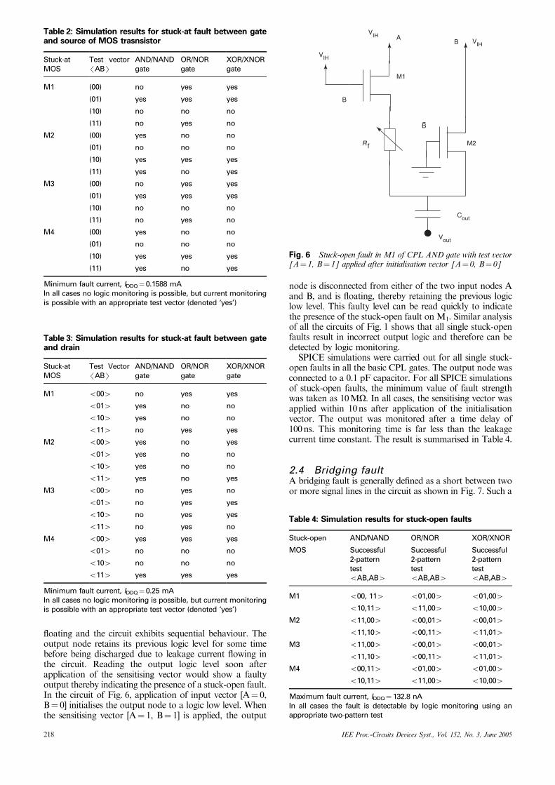
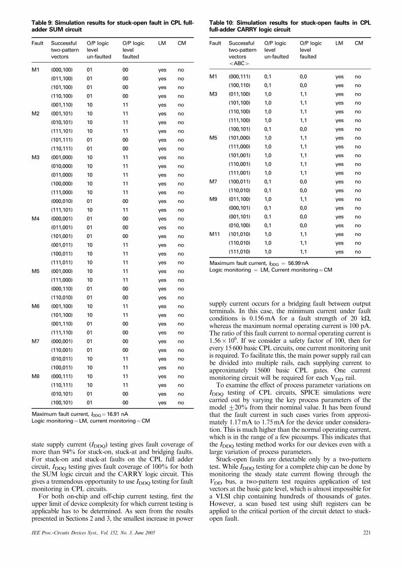
3.3 Stuck-open faultSimilar fault analysis and SPICE simulations have beenperformed for stuck-open faults on all transistors of SUMlogic and CARRY logic circuits of the full-adder. Simula-tion results are summarised in Tables 9 and 10.
4 Testability issues of CPL circuits
The qualitative analysis and simulation results presented inSections 2 and 3 show that for CPL basic circuits steady-
M5 M7
M4
R f
M3
C
VIHVIH
VIH
VIH
Vout
A
A
C
Fig. 10 Equivalent circuit for stuck-on fault on M5 of CPL full-adder SUM circuit for test vector [A¼ 0, B¼ 0, C¼ 1]
Table 5: Simulation results for stuck-on faults in CPL full-adder SUM circuit
Fault Successful test vector oABC4 LM CM
M1 (000),(001), (010), (011) no yes
M2 (000),(001), (010), (011) no yes
M3 (100),(101), (110), (111) no yes
M4 (100),(101), (110), (111) no yes
M5 (001),(011), (101), (111) no yes
M6 (001),(011), (101), (111) no yes
M7 (000),(010), (100), (110) no yes
M8 (000),(010), (100), (110) no yes
Minimum fault current, IDDQO¼0.194mALogic monitoring¼LM, current monitoring¼CM
Table 6: Simulation results for stuck-on faults in CPL full-adder CARRY circuit
Fault Successful Test Vector oABC4 LM CM
M1 (001),(100) no yes
M3 (011),(110) no yes
M5 (011),(110) no yes
M7 (001),(100) no yes
M9 (001),(011) no yes
M11 (100),(110) no yes
Minimum fault current, IDDQ¼ 0.195mALogic monitoring¼LM, current monitoring¼CM
Table 7: Simulation results for stuck-at faults in CPL full-adder SUM circuit
Fault Successful Test Vector oABC4 LM CM
M1 (010),(011), (110), (111) no yes
M2 (000),(001), (100), (101) no yes
M3 (000),(001), (100), (101) no yes
M4 (010),(011), (110), (111) no yes
M5 (000),(001), (110), (111) no yes
M6 (010),(011), (100), (101) no yes
M7 (010),(011), (100), (101) no yes
M8 (000),(001), (110), (111) no yes
Minimum fault current, IDDQ¼ 0.232 mALogic monitoring¼LM, current monitoring¼CM
Table 8: Simulation results for stuck-at faults in CPL full-adder CARRY logic circuit
Fault Successful test vector oABC4 LM CM
M1 (001), (010) (011),(101) no yes
M3 (000),(100) (110),(111) no yes
M5 (000),(001) (011),(111) no yes
M7 (010),(100) (101),(110) no yes
M9 (011), (100) no yes
M11 (000),(001) (010),(101) (110),(111) no yes
Minimum fault current, IDDQ¼ 0.2329 mALogic monitoring¼LM, current monitoring¼CM
220 IEE Proc.-Circuits Devices Syst., Vol. 152, No. 3, June 2005
state supply current (IDDQ) testing gives fault coverage ofmore than 94% for stuck-on, stuck-at and bridging faults.For stuck-on and stuck-at faults on the CPL full addercircuit, IDDQ testing gives fault coverage of 100% for boththe SUM logic circuit and the CARRY logic circuit. Thisgives a tremendous opportunity to use IDDQ testing for faultmonitoring in CPL circuits.
For both on-chip and off-chip current testing, first theupper limit of device complexity for which current testing isapplicable has to be determined. As seen from the resultspresented in Sections 2 and 3, the smallest increase in power
supply current occurs for a bridging fault between outputterminals. In this case, the minimum current under faultconditions is 0.156mA for a fault strength of 20 kO,whereas the maximum normal operating current is 100 pA.The ratio of this fault current to normal operating current is1.56 106. If we consider a safety factor of 100, then forevery 15600 basic CPL circuits, one current monitoring unitis required. To facilitate this, the main power supply rail canbe divided into multiple rails, each supplying current toapproximately 15600 basic CPL gates. One currentmonitoring circuit will be required for each VDD rail.
To examine the effect of process parameter variations onIDDQ testing of CPL circuits, SPICE simulations werecarried out by varying the key process parameters of themodel 720% from their nominal value. It has been foundthat the fault current in such cases varies from approxi-mately 1.17mA to 1.75mA for the device under considera-tion. This is much higher than the normal operating current,which is in the range of a few picoamps. This indicates thatthe IDDQ testing method works for our devices even with alarge variation of process parameters.
Stuck-open faults are detectable only by a two-patterntest. While IDDQ testing for a complete chip can be done bymonitoring the steady state current flowing through theVDD bus, a two-pattern test requires application of testvectors at the basic gate level, which is almost impossible fora VLSI chip containing hundreds of thousands of gates.However, a scan based test using shift registers can beapplied to the critical portion of the circuit detect to stuck-open fault.
Table 9: Simulation results for stuck-open fault in CPL full-adder SUM circuit
Fault Successfultwo-patternvectors
O/P logiclevelun-faulted
O/P logiclevelfaulted
LM CM
M1 (000,100) 01 00 yes no
(011,100) 01 00 yes no
(101,100) 01 00 yes no
(110,100) 01 00 yes no
(001,110) 10 11 yes no
M2 (001,101) 10 11 yes no
(010,101) 10 11 yes no
(111,101) 10 11 yes no
(101,111) 01 00 yes no
(110,111) 01 00 yes no
M3 (001,000) 10 11 yes no
(010,000) 10 11 yes no
(011,000) 10 11 yes no
(100,000) 10 11 yes no
(111,000) 10 11 yes no
(000,010) 01 00 yes no
(111,101) 10 11 yes no
M4 (000,001) 01 00 yes no
(011,001) 01 00 yes no
(101,001) 01 00 yes no
(001,011) 10 11 yes no
(100,011) 10 11 yes no
(111,011) 10 11 yes no
M5 (001,000) 10 11 yes no
(111,000) 10 11 yes no
(000,110) 01 00 yes no
(110,010) 01 00 yes no
M6 (001,100) 10 11 yes no
(101,100) 10 11 yes no
(001,110) 01 00 yes no
(111,110) 01 00 yes no
M7 (000,001) 01 00 yes no
(110,001) 01 00 yes no
(010,011) 10 11 yes no
(100,011) 10 11 yes no
M8 (000,111) 10 11 yes no
(110,111) 10 11 yes no
(010,101) 01 00 yes no
(100,101) 01 00 yes no
Maximum fault current, IDDQ¼16.91 nALogic monitoring¼LM, current monitoring¼CM
Table 10: Simulation results for stuck-open faults in CPLfull-adder CARRY logic circuit
Fault Successfultwo-patternvectorsoABC4
O/P logiclevelun-faulted
O/P logiclevelfaulted
LM CM
M1 (000,111) 0,1 0,0 yes no
(100,110) 0,1 0,0 yes no
M3 (011,100) 1,0 1,1 yes no
(101,100) 1,0 1,1 yes no
(110,100) 1,0 1,1 yes no
(111,100) 1,0 1,1 yes no
(100,101) 0,1 0,0 yes no
M5 (101,000) 1,0 1,1 yes no
(111,000) 1,0 1,1 yes no
(101,001) 1,0 1,1 yes no
(110,001) 1,0 1,1 yes no
(111,001) 1,0 1,1 yes no
M7 (100,011) 0,1 0,0 yes no
(110,010) 0,1 0,0 yes no
M9 (011,100) 1,0 1,1 yes no
(000,101) 0,1 0,0 yes no
(001,101) 0,1 0,0 yes no
(010,100) 0,1 0,0 yes no
M11 (101,010) 1,0 1,1 yes no
(110,010) 1,0 1,1 yes no
(111,010) 1,0 1,1 yes no
Maximum fault current, IDDQ ¼ 56.99nALogic monitoring ¼ LM, Current monitoring¼CM
IEE Proc.-Circuits Devices Syst., Vol. 152, No. 3, June 2005 221
There are many new defect mechanisms affectingadvanced CMOS technologies. These are gate oxide failure,ultra-thin oxide reliability etc. Dielectric breakdown of gateoxide would turn on the drain-back-gate or source-back-gate junction and a large forward current would flow, whichcould be detected by IDDQ testing. However, gate oxidethickness reduction in deep submicron technology couldlead to parametric failure. Parametric failure in CMOS ICsleads to severe detection problem. Detection of these newtypes of fault is still a nascent research area and much workis being done to overcome the difficulties [16–18].
5 Conclusions
Theoretical analysis and SPICE simulations of the testabi-lity of basic CPL circuits under various single stuck faultshas been presented. It was found that all stuck-on faults onall CPL basic gates were detected by current monitoring butno logic monitoring was possible. Similar results have beenobtained for stuck-at faults between gate and source of theMOS devices of all basic CPL gates. However, for stuck-atfaults between gate and drain, it was found that all stuck-atfaults between gate and drain could be detected by currentmonitoring except for the following two MOS devices: (i)MOS M3 of the basic AND/NAND gate and (ii) MOS M2
of the basic OR/NOR gate for which the gate and drainterminals have the same input variable. In the case of stuck-open faults, it was found that stuck-open faults on all MOStransistors of all basic CPL gates were detected with logicmonitoring by applying an appropriate two-pattern test.Stuck-at and stuck-on are the most common faults on VLSIcircuits and for CPL basic gate circuits IDDQ testing givesfault coverage of more than 94% for stuck-at, stuck-on andbridging faults. In the case of a CPL full-adder, we havefound that stuck-on and stuck-at faults on all transistors ofSUM logic and CARRY logic circuits can be detected bycurrent monitoring, i.e. IDDQ testing provides 100% faultcoverage. Like CPL basic circuits, stuck-open faults on alltransistors of a CPL full-adder are detectable by logicmonitoring applying an appropriate two-pattern test.Therefore, it can be concluded that signal source currentmonitoring (IDDQ testing) is the best method for commonfault detection in CPL circuits and that it gives a very widerange of fault coverage. Again for detecting stuck-openfaults, logic monitoring with a two-pattern test is the onlyavailable method so far and for CPL basic circuits it givesfault coverage of 100%. Therefore, other than low power
consumption, higher speed and higher logic functionality,CPL circuits are also very promising from a testability pointof view.
6 References
1 Yano, K., Yamanaka, T., Nishida, T., Saito, M., Shimohigashi, K.,and Shimizu, A.: ‘A 3.8ns CMOS 16 16 -b multiplier usingcomplementary pass-transistor logic’, IEEE J. Solid-State Circuits,1990, 25, (2), pp. 388–395
2 Avci, M., and Yildirim, T.: ‘General design method for complemen-tary pass transistor logic circuits’, Electron. Lett., 2003, 39, (1),pp. 46–48
3 Abu-Khater, I.S., Bellaouar, A., and Elmasry, M.I.: ‘Circuittechniques for CMOS low-power high-performance multipliers’, IEEEJ. Solid-State Circuits, 1996, 31, (10), pp. 1535–1546
4 Abu-Khater, I.S., Bellaouar, A., Elmasry, M.I., and Yan, R.H.:‘Circuit/architecture for low-power high-performance 32-bit adder’.Proc. IEEE 5th Great Lakes Symp. on VLSI, Buffalo, NY, USA,1995, pp. 74–77
5 Strallo, A.G.M., and Napoli, E.: ‘A fast and area efficientcomplimentary pass-transistor logic carry-skip adder’. Proc. 21st Int.Conf. on Microelectronics, MIEL, 1997, Vol. 2, pp. 701–704
6 Wang, L.K., and Chen, H.H.: ‘A low power high speed errorcorrection code macro using complementary pass-transistor logic’.Proc. 10th Annual IEEE Int. ASIC Conf. and Exhibition, 1997,pp. 17–20
7 Fuse, T., Oowaki, Y., and Terauchi, M.: ‘An ultra low voltage SOICMOS pass-gate logic’, IEICE Trans. Electron, 1997, E80-C, (3),pp. 472–477
8 ‘IBM S/390 G3 and G4’, IBM J. Res. Dev., 1997, 41, special issue,Nos. 4/5, July/Sept. 1997
9 Williams, T., and Parker, K.: ‘Design for testability - a survey’, IEEETrans. Comput., 1982, C-31, pp. 2–15
10 Aziz, S.M., Rashid, A.B.M.H., and Karim, M.: ‘Fault characteriza-tion of complementary pass-transistor logic circuits’. Proc. IEEE Int.Conf. on Semiconductor Electronics, Malaysia, 2000, pp. 80–84
11 Rashid, A.B.M.H., Karim, M., and Aziz, S.M.: ‘Testing complemen-tary pass-transistor logic circuits’. Proc. IEEE Int. Symp. on Circuitsand Systems (ISCAS 2001), Sydney, Australia, 2001, Vol. 4, pp. 5–8
12 Jha, N.K., and Kundu, S.: ‘Testing and reliable design of CMOScircuits’ (Kluwer Academic Publishers, USA, 1990)
13 Wadsack, R.L.: ‘Fault modeling and logic simulation ofCMOS and MOS integrated circuits’, Bell Syst. Tech. J., 1978, 57,(5), pp. 1449–1474
14 Maly, W., Nag, P.K., and Nigh, P.: ‘Testing oriented analysis ofCMOS ICs with opens’. Proc. Int. Conf. on Computer-Aided Design,Santa Clara, CA, 1995, pp. 344–347
15 Mei, K.C.Y.: ‘Bridging and stuck-at faults’, IEEE Trans. Comput.,1974, C-23, (7), pp. 720–727
16 Bernardini, S., Portal, J. M., and Masson, P.: ‘A tunneling model forgate oxide failure in deep sub-micron technology’. Proc. Design,Automation and Test in Europe (DATE) Conf., 16–20 Feb 2004,Vol. 2, pp. 1404–1405
17 Dragic, S., and Margala, M.: ‘A 1.2V built-in architecture for highfrequency on-line IDDQ/delta IDDQ test’. Proc. IEEE ComputerSociety Annual Symp. on VLSI, Pittsburg, USA, 25–26 April,pp. 148–153
18 Powell, T.J., Pair, J., St. John, M., and Counce, D.: ‘Delta IDDQ fortesting reliability’. Proc. 18th IEEE VLSI Symp., Montreal, Canada,4–5 April 2000, pp. 439–443
222 IEE Proc.-Circuits Devices Syst., Vol. 152, No. 3, June 2005
Copyright © 2022 FDOKUMEN