The Field-Effect Transistor (FET)
69
中央大學通訊系 張大中 Electronics I, Neamen 3th Ed. 1 The Field-Effect Transistor (FET) 張大中 中央大學 通訊工程系 [email protected] CO2005: Electronics I
-
Upload
khangminh22 -
Category
Documents
-
view
3 -
download
0
Transcript of The Field-Effect Transistor (FET)

中央大學通訊系 張大中 Electronics I, Neamen 3th Ed. 1
The Field-Effect Transistor(FET)
張大中中央大學 通訊工程系
CO2005: Electronics I

中央大學通訊系 張大中 Electronics I, Neamen 3th Ed. 2
The metal-oxide-semiconductor field-effect transistor (MOSFET) becomes a practicalreality in the 1970s.
The MOSFET, compared to BJTs, can be made very small, that is, it occupies a very smallarea in IC chip.
In the MOSFET, the current is controlled by an electric field applied perpendicular to boththe semiconductor surface and to the direction of current.
The phenomenon applying an electric field perpendicular to the surface is called the fieldeffect.
Basic MOS capacitor structure
MOSFET

中央大學通訊系 張大中 Electronics I, Neamen 3th Ed. 3
The Physics of the MOS Capacitor
Gate
中央大學通訊系 張大中 Electronics I, Neamen 3th Ed. 4
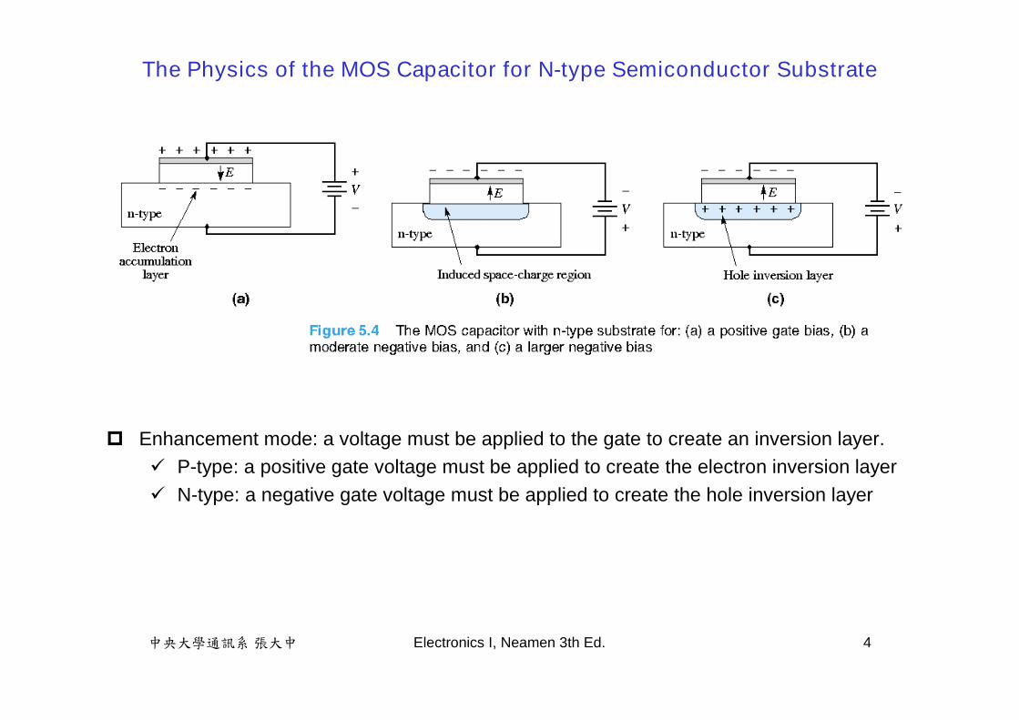
Enhancement mode: a voltage must be applied to the gate to create an inversion layer. P-type: a positive gate voltage must be applied to create the electron inversion layer N-type: a negative gate voltage must be applied to create the hole inversion layer
The Physics of the MOS Capacitor for N-type Semiconductor Substrate

中央大學通訊系 張大中 Electronics I, Neamen 3th Ed. 5
Transistor Structure
Transistor Operation
NMOS
Large enough positivevoltage induces anelectron inversion layer.
Connection between D andS is created so that acurrent can be generated.

中央大學通訊系 張大中 Electronics I, Neamen 3th Ed. 6
The threshold voltage of the n-channel MOSFET is denoted as and is defined as theapplied gate voltage needed to create an inversion charge.
We can think of the threshold voltage as the gate voltage required to “turn on”thetransistor.
MOSFET Current-Voltage Characteristics
TNV

中央大學通訊系 張大中 Electronics I, Neamen 3th Ed. 7
The versus characteristics for small values of
MOSFET Current-Voltage Characteristics
Di DSv DSv

中央大學通訊系 張大中 Electronics I, Neamen 3th Ed. 8
MOSFET Current-Voltage Characteristics

中央大學通訊系 張大中 Electronics I, Neamen 3th Ed. 9
Nonsaturation (triode) Region
Saturation Region
Ideal MOSFET Current-Voltage Characteristics
TNGSsatDSDS Vvvv )(
)2(])(2[ 2)(
2DSDSsatDSnDSDSTNGSnD vvvKvvVvKi
)also()( TNGSsatDSDS Vvvv 2)( TNGSnD VvKi
DSDo
vir
/1
Note: In the saturation region,

中央大學通訊系 張大中 Electronics I, Neamen 3th Ed. 10
Conduction Parameter
The conduction parameter is a function of both electrical and geometric parameters. Electrical Parameters: The oxide capacitance and carrier mobility are essentially
constants for a given technology.
Geometrical Parameters: The width-to-length ratio (W/L) is a variable in the design ofMOSFETs that is used to produce specific current-voltage characteritics in MOSFETcircuits.
Conduction Parameter
2oxn
nC
LW
K (conduction parameter)
oxC
nWL
: oxide capacitance per unit area
: electron mobility
: channel width
: channel length
thicknessoxide:,1
oxox
ox tt
C
constant:2 nn
n kk
LW
K
中央大學通訊系 張大中 Electronics I, Neamen 3th Ed. 11

中央大學通訊系 張大中 Electronics I, Neamen 3th Ed. 12
In the p-channel enhancement-mode device, a negative gate-to-source voltage must beapplied to create the inversion layer of holes that connects the source and drain regions.
The threshold voltage, denoted an for the PMOS is negative for an enhancement-mode devices. The threshold voltage is positive for a depletion-mode device.
Holes flow from the source to the drain, the conventional current enters the source andleaves the drain.
PMOS
TPV

中央大學通訊系 張大中 Electronics I, Neamen 3th Ed. 13
Nonsaturation (triode) Region
Saturation Region
Ideal PMOS Current-Voltage Relationship
:when )( TPSGsatSDSD Vvvv
)2(])(2[ 2)(
2SDSDsatSDpSDSDTPSGpD vvvKvvVvKi
:)0also(when )( TPSGsatSDSD Vvvv 2)( TPSGpD VvKi

中央大學通訊系 張大中 Electronics I, Neamen 3th Ed. 14
Circuit Symbols
N-channel enhancement-mode MOSFET
P-channel enhancement-mode MOSFET
中央大學通訊系 張大中 Electronics I, Neamen 3th Ed. 15
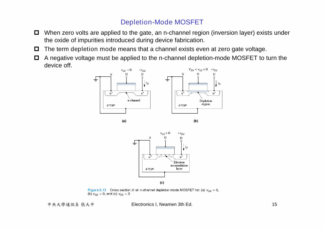
When zero volts are applied to the gate, an n-channel region (inversion layer) exists underthe oxide of impurities introduced during device fabrication.
The term depletion mode means that a channel exists even at zero gate voltage. A negative voltage must be applied to the n-channel depletion-mode MOSFET to turn the
device off.
Depletion-Mode MOSFET

中央大學通訊系 張大中 Electronics I, Neamen 3th Ed. 16
I-V Curves and Circuit Symbols for Depletion-mode MOSFET
中央大學通訊系 張大中 Electronics I, Neamen 3th Ed. 17
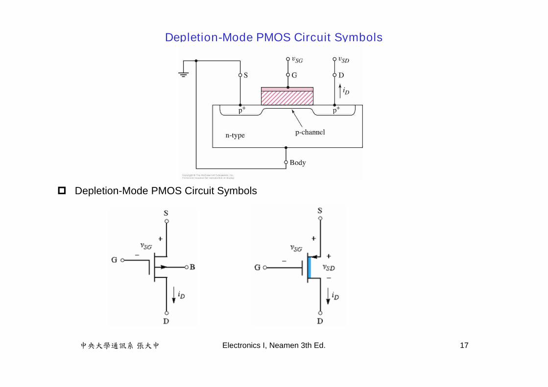
Depletion-Mode PMOS Circuit Symbols
Depletion-Mode PMOS Circuit Symbols

中央大學通訊系 張大中 Electronics I, Neamen 3th Ed. 18
Complement MOS (CMOS) technology uses both NMOS and PMOS in the same circuit. To design electrically equivalent NMOS and PMOS devices, adjusting the W/L ratios of the
transistors is required.
CMOS

中央大學通訊系 張大中 Electronics I, Neamen 3th Ed. 19
Summary of MOS Transistor Operation
中央大學通訊系 張大中 Electronics I, Neamen 3th Ed. 20
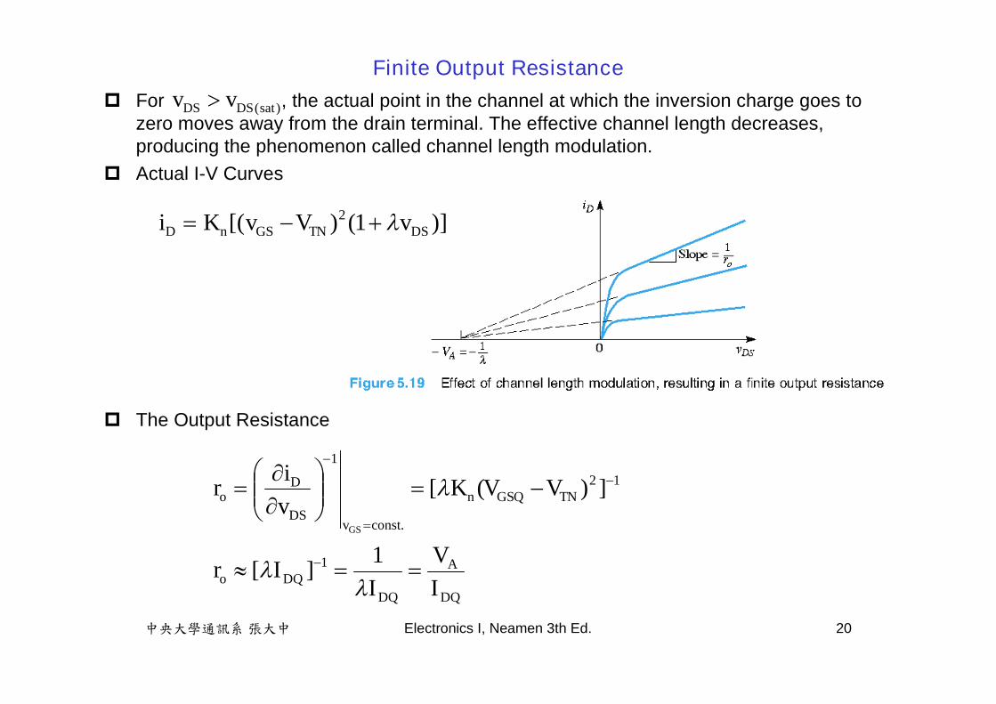
For , the actual point in the channel at which the inversion charge goes tozero moves away from the drain terminal. The effective channel length decreases,producing the phenomenon called channel length modulation.
Actual I-V Curves
The Output Resistance
Finite Output Resistance
)]1()[( 2DSTNGSnD vVvKi
12
const.
1
])([
TNGSQn
vDS
Do VVK
vi
r
GS
DQ
A
DQDQo I
VI
Ir
1
][ 1
)sat(DSDS vv
中央大學通訊系 張大中 Electronics I, Neamen 3th Ed. 21
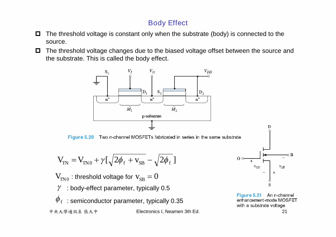
The threshold voltage is constant only when the substrate (body) is connected to thesource.
The threshold voltage changes due to the biased voltage offset between the source andthe substrate. This is called the body effect.
Body Effect
]22[0 fSBfTNTN vVV
0TNV
f
: threshold voltage for
: body-effect parameter, typically 0.5
: semiconductor parameter, typically 0.35
0SBv
中央大學通訊系 張大中 Electronics I, Neamen 3th Ed. 22
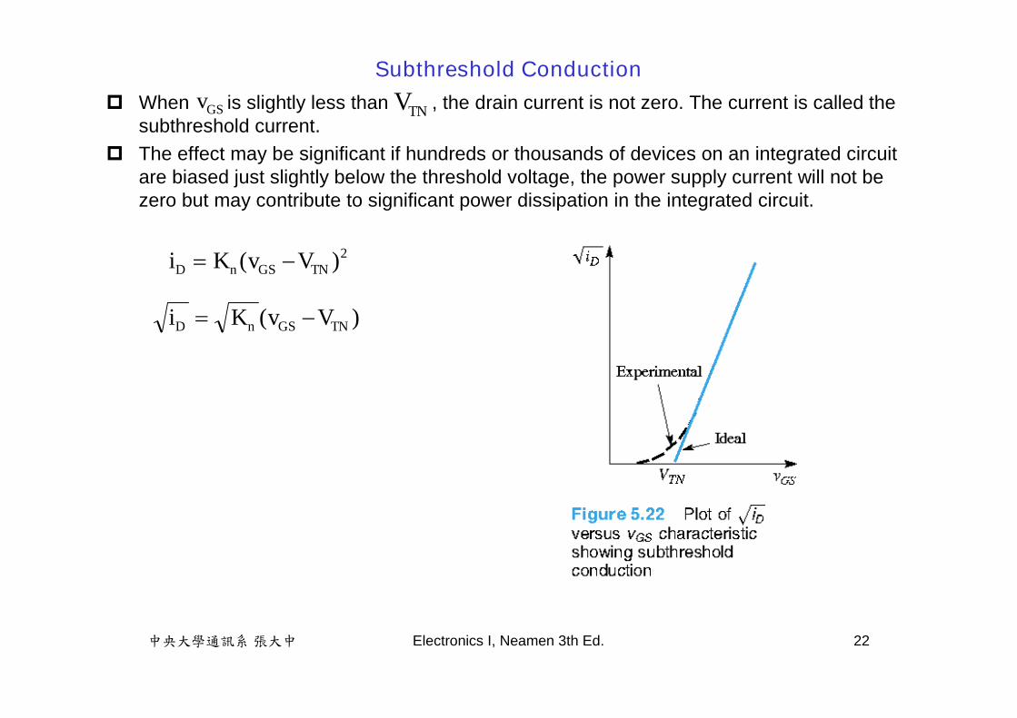
When is slightly less than , the drain current is not zero. The current is called thesubthreshold current.
The effect may be significant if hundreds or thousands of devices on an integrated circuitare biased just slightly below the threshold voltage, the power supply current will not bezero but may contribute to significant power dissipation in the integrated circuit.
Subthreshold Conduction
GSv TNV
2)( TNGSnD VvKi
)( TNGSnD VvKi

中央大學通訊系 張大中 Electronics I, Neamen 3th Ed. 23
Breakdown: The drain-to-substrate pn junction may break down if the applied drainvoltage is too high and avalanche multiplication occurs. The breakdown is the samereverse-biased pn junction breakdown.
Punch-through: when the drain voltage is large enough for the depletion region aroundthe drain to extend completely through the channel to the source terminal. This effectcauses the drain current to increase rapidly with only a small increase in drain voltage.
Near-avalanche: The source-substrate-drain structure is equivalent to that of a bipolartransistor. As the device size shrinks, we may begin to see a parasitic bipolar transistoraction with increases in the drain voltage. This parasitic action enhances the breakdowneffect.
If the electric field in the oxide becomes large enough, breakdown can also occur in theoxide, which can lead to catastrophic failure.
Temperature Effect Threshold voltage decreases with temperature, thus the drain current increases with
temperature with a given . The conduction parameter decreases as the temperature increases. The net effect of increasing temperature is a decrease in drain current at a given .
Breakdown and Temperature Effects
GSV
GSV

中央大學通訊系 張大中 Electronics I, Neamen 3th Ed. 24
NMOS Common-Source Circuit
中央大學通訊系 張大中 Electronics I, Neamen 3th Ed. 25
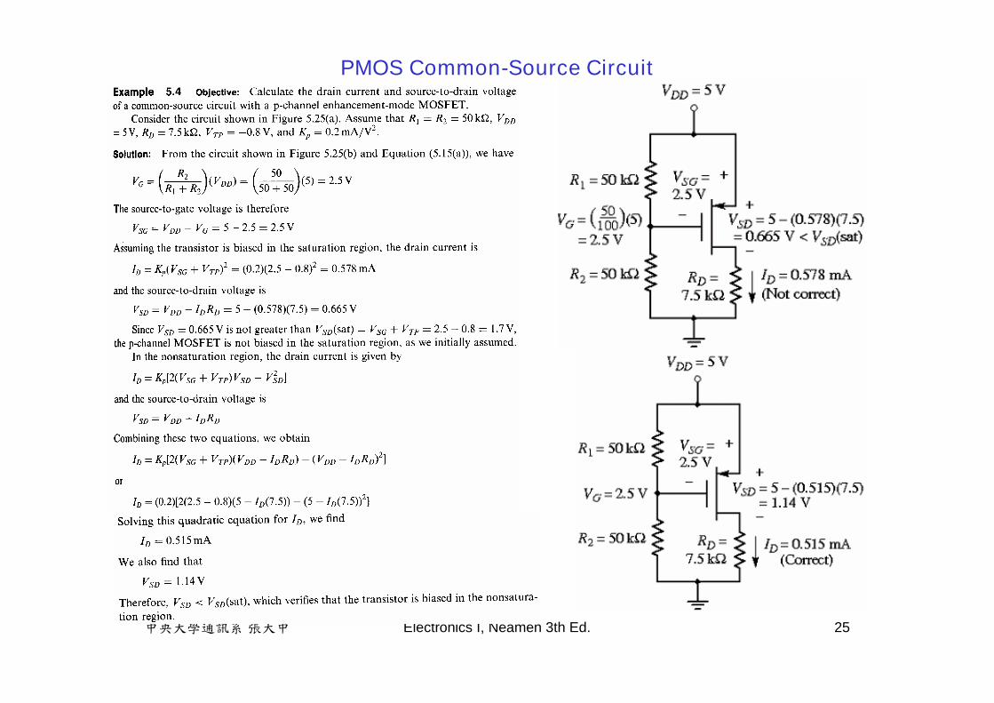
PMOS Common-Source Circuit
中央大學通訊系 張大中 Electronics I, Neamen 3th Ed. 26
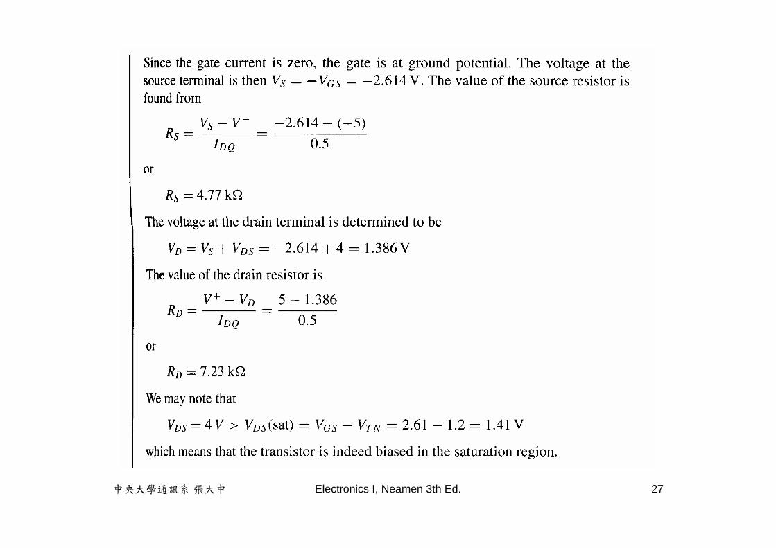
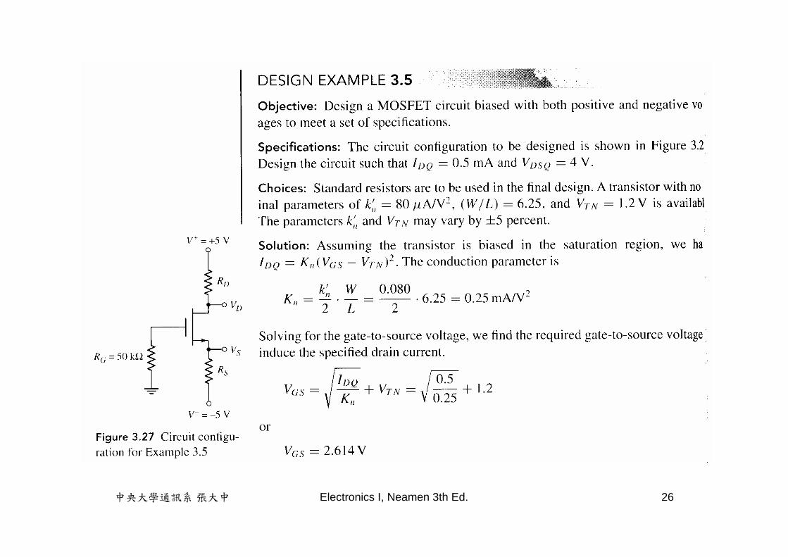
中央大學通訊系 張大中 Electronics I, Neamen 3th Ed. 27
中央大學通訊系 張大中 Electronics I, Neamen 3th Ed. 28
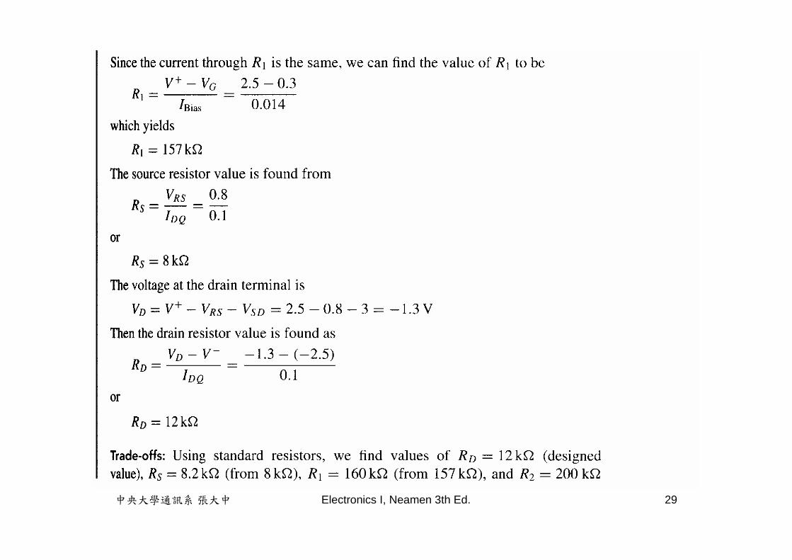
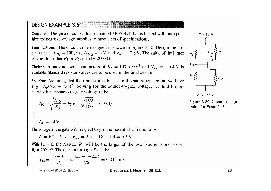
中央大學通訊系 張大中 Electronics I, Neamen 3th Ed. 29

中央大學通訊系 張大中 Electronics I, Neamen 3th Ed. 30
中央大學通訊系 張大中 Electronics I, Neamen 3th Ed. 31
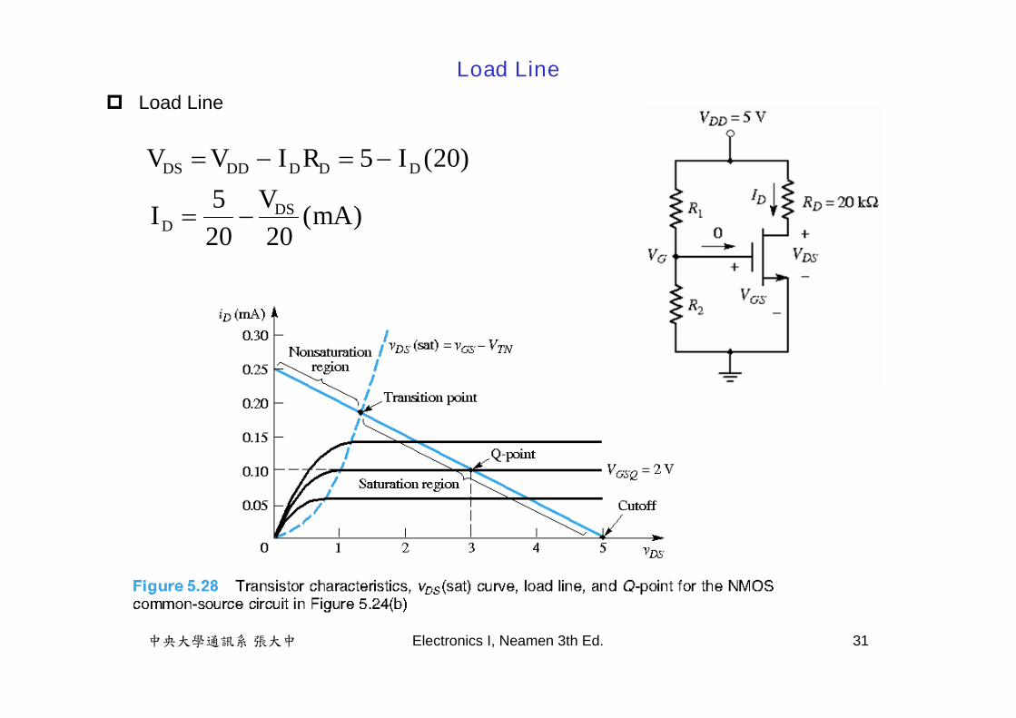
Load Line
Load Line
)mA(2020
5
)20(5
DSD
DDDDDDS
VI
IRIVV

中央大學通訊系 張大中 Electronics I, Neamen 3th Ed. 32

中央大學通訊系 張大中 Electronics I, Neamen 3th Ed. 33

中央大學通訊系 張大中 Electronics I, Neamen 3th Ed. 34

中央大學通訊系 張大中 Electronics I, Neamen 3th Ed. 35

中央大學通訊系 張大中 Electronics I, Neamen 3th Ed. 36
An enhancement-mode MOSFET is used as a nonlinear resistor. The transistor is always biased in the saturation region and called a load device.
Nonlinear Resistor
22
)(
)()(
0,
TNDSnTNGSnD
TNTNGSSatDSGSDS
VvKVvKi
VVvvvv
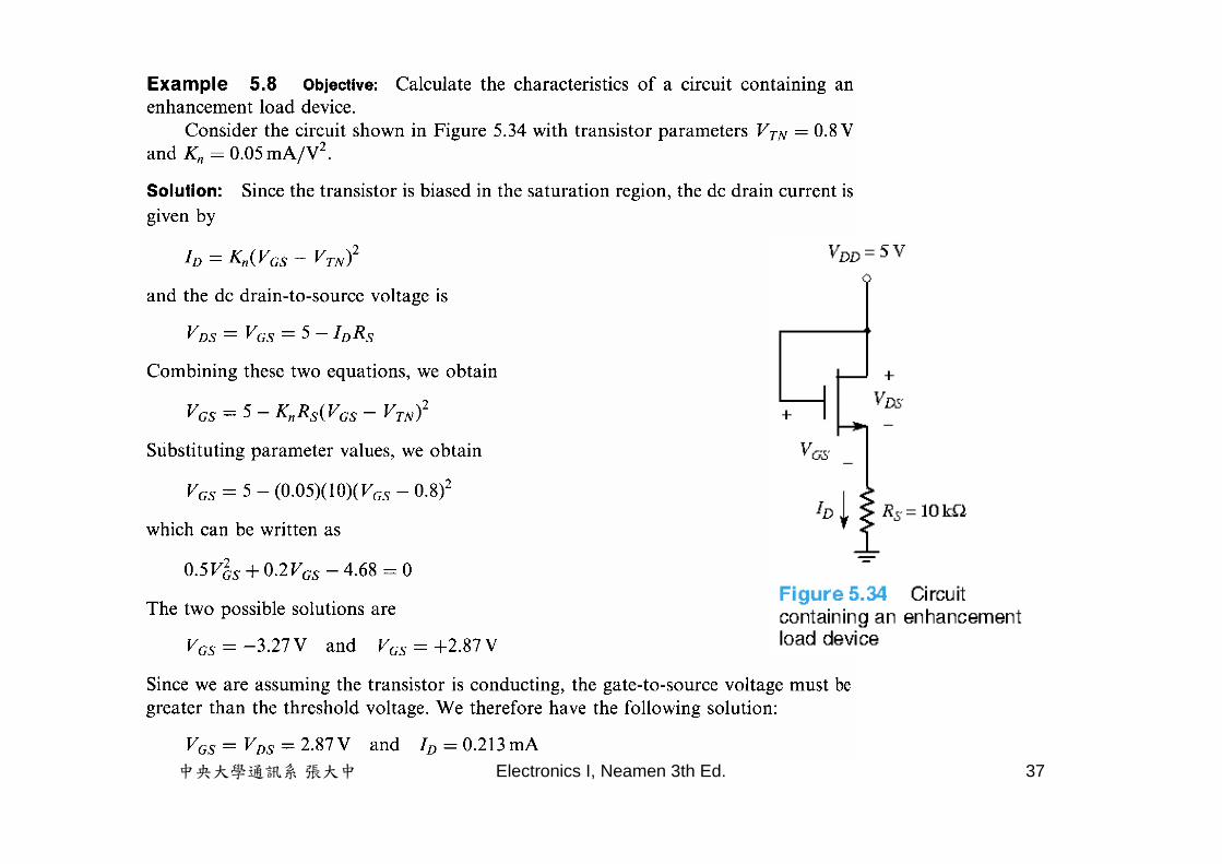
中央大學通訊系 張大中 Electronics I, Neamen 3th Ed. 37
中央大學通訊系 張大中 Electronics I, Neamen 3th Ed. 38

中央大學通訊系 張大中 Electronics I, Neamen 3th Ed. 39

中央大學通訊系 張大中 Electronics I, Neamen 3th Ed. 40
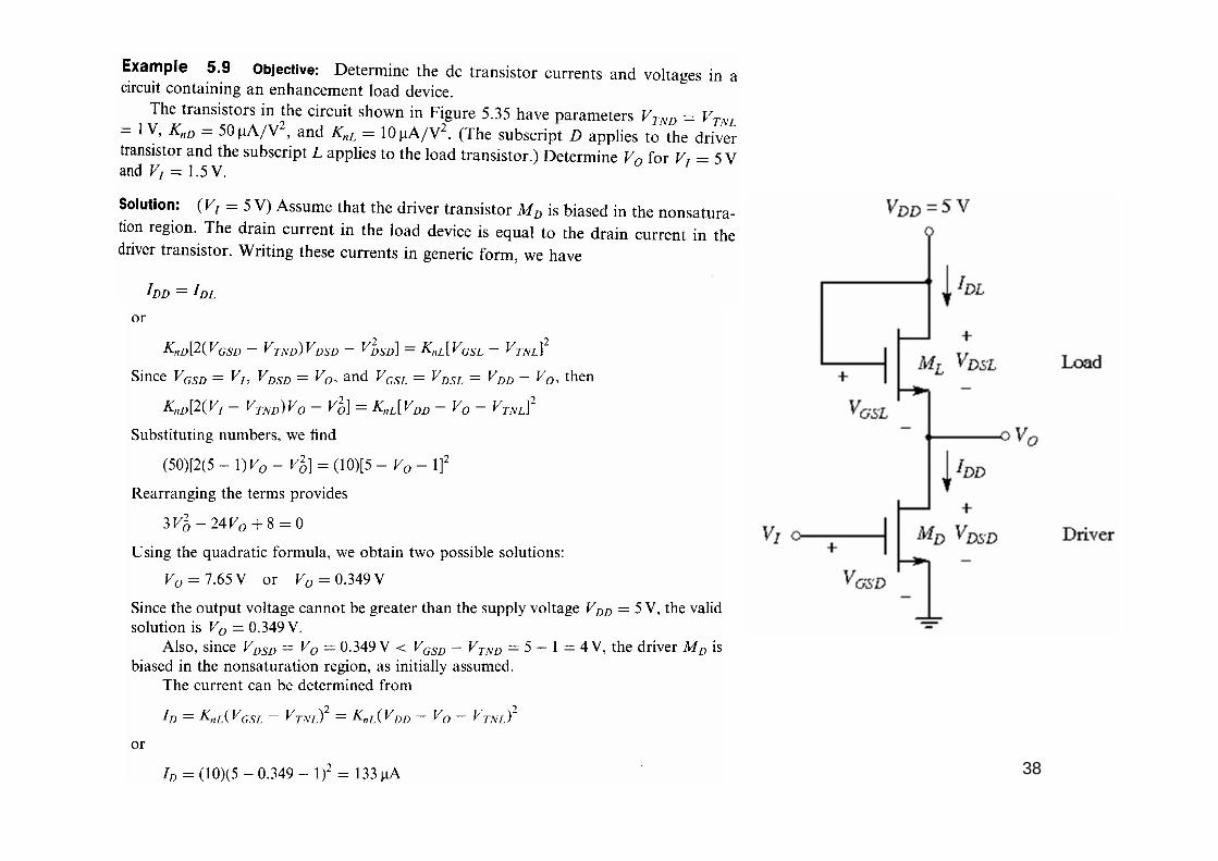
The Transition Point for Saturation and Non-saturation Regions(1) Load Device Transistor Characteristics
(2) Transition Point for the Driver Transistor
(3) For the transition input voltage
2
2
)(
)(
OTNLDDnL
TNLGSLnLDL
VVVK
VVKI
TNDGSDSatDSD VVV )(
The current in the saturation region,2
)(2
)( )( SatDSDnDTNDGSDnDSatDD VKVVKI
ItGSD VV
The transition output voltage TNDItSatDSDOtO VVVVV )(
DLSatDD II )(
22 )()( TNDItTNLDDnLTNDItnD VVVVKVVK
)()( TNDItTNLDDnLTNDItnD VVVVKVVK
nLnD
nLnDTNDTNLDDIt KK
KKVVVV
/1)/1(
)(SatDDI DLI
DSDVOtV
DDQI
DDI
TNLDD VV
ItV
ItV
OtV

中央大學通訊系 張大中 Electronics I, Neamen 3th Ed. 41
Depletion-mode MOSFET as a Load Device

中央大學通訊系 張大中 Electronics I, Neamen 3th Ed. 42

中央大學通訊系 張大中 Electronics I, Neamen 3th Ed. 43
CMOS Inverter

中央大學通訊系 張大中 Electronics I, Neamen 3th Ed. 44
If , the transistor is in cut-off.
If (and make ), the transistor is biased in the non-saturation region.
NMOS Inverter
TNI Vv
DDO
DVv
i0
TNI Vv
DDDDO
OOTNInD
RivvvvVvKi
])(2[ 2
DSTNI vVv
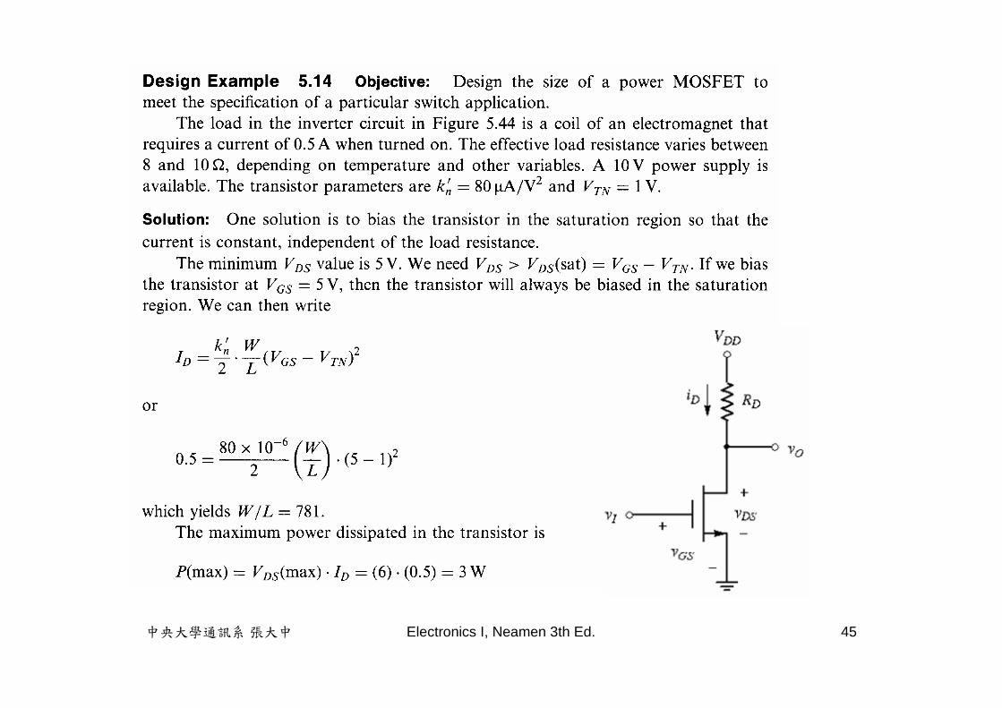
中央大學通訊系 張大中 Electronics I, Neamen 3th Ed. 45

中央大學通訊系 張大中 Electronics I, Neamen 3th Ed. 46
Digital Logic Gate

中央大學通訊系 張大中 Electronics I, Neamen 3th Ed. 47
We can establish a particular Q-point on the load line by designing the ratio of the biasresistors and .
MOS Small-Signal Amplifier
1R 2R

中央大學通訊系 張大中 Electronics I, Neamen 3th Ed. 48
Constant-Current Biasing
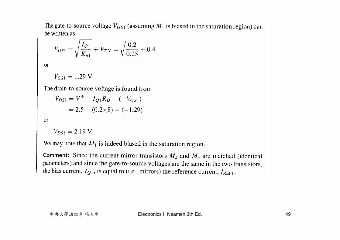
中央大學通訊系 張大中 Electronics I, Neamen 3th Ed. 49

中央大學通訊系 張大中 Electronics I, Neamen 3th Ed. 50

中央大學通訊系 張大中 Electronics I, Neamen 3th Ed. 51

中央大學通訊系 張大中 Electronics I, Neamen 3th Ed. 52
Constant-Current Biasing
2444
2333 )()( TNGSnTNGSn VVKVVK
VVV GSGS 34
43
43343 /1
/
nn
nnTNTNGS KK
KKVVVV
2232 )( TNGSnQ VVKI

中央大學通訊系 張大中 Electronics I, Neamen 3th Ed. 53
中央大學通訊系 張大中 Electronics I, Neamen 3th Ed. 54
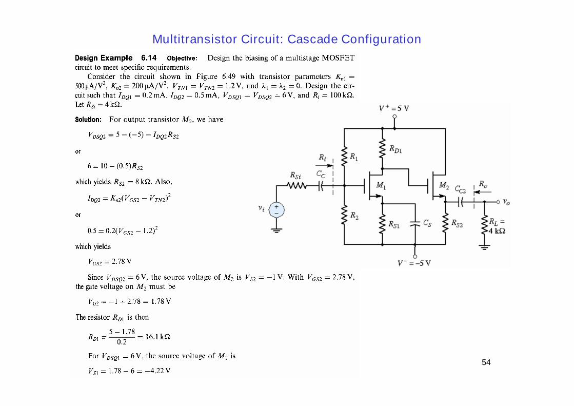
Multitransistor Circuit: Cascade Configuration

中央大學通訊系 張大中 Electronics I, Neamen 3th Ed. 55

中央大學通訊系 張大中 Electronics I, Neamen 3th Ed. 56
Multitransistor Circuit: Cascode Configuration
中央大學通訊系 張大中 Electronics I, Neamen 3th Ed. 57

中央大學通訊系 張大中 Electronics I, Neamen 3th Ed. 58
Cross Section Structure
IV curves for small drain-to-source voltages
PN Junction Field-Effect Transistor
Pinchoff

中央大學通訊系 張大中 Electronics I, Neamen 3th Ed. 59
The drain voltage changes for a given gate voltage.
PN JFET
中央大學通訊系 張大中 Electronics I, Neamen 3th Ed. 60
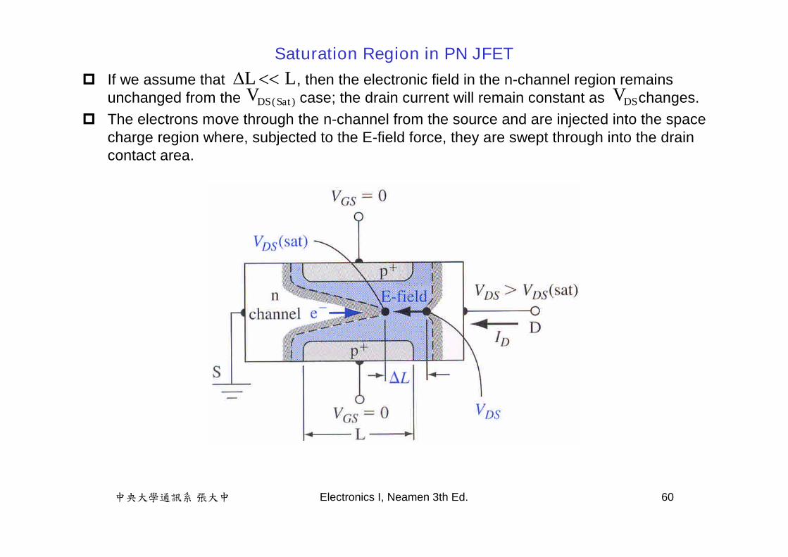
If we assume that , then the electronic field in the n-channel region remainsunchanged from the case; the drain current will remain constant as changes.
The electrons move through the n-channel from the source and are injected into the spacecharge region where, subjected to the E-field force, they are swept through into the draincontact area.
Saturation Region in PN JFETLL
)(SatDSV DSV

中央大學通訊系 張大中 Electronics I, Neamen 3th Ed. 61
A reverse-bias gate-to-source voltage induces a space-charge region under the metal gate,which modulates the channel conductance.
If a negative applied gate voltage is sufficiently large, the space-charge region willeventually reach the substrate, the pinchoff will occur.
It is equivalent to an n-channel depletion-mode device, since a gate voltage must beapplied to pinch off the channel.
N-Channel Depletion-mode MESFET

中央大學通訊系 張大中 Electronics I, Neamen 3th Ed. 62
The channel is pinched off even at . To open the channel, the depletion region must be reduced; that is, a forward-biased
voltage is applied to the gate-semiconductor (G-S) junction. The threshold voltage is the gate-to-source voltage required to create the pinch-off
condition.
N-Channel Enhancement-mode MESFET0GSv
中央大學通訊系 張大中 Electronics I, Neamen 3th Ed. 63
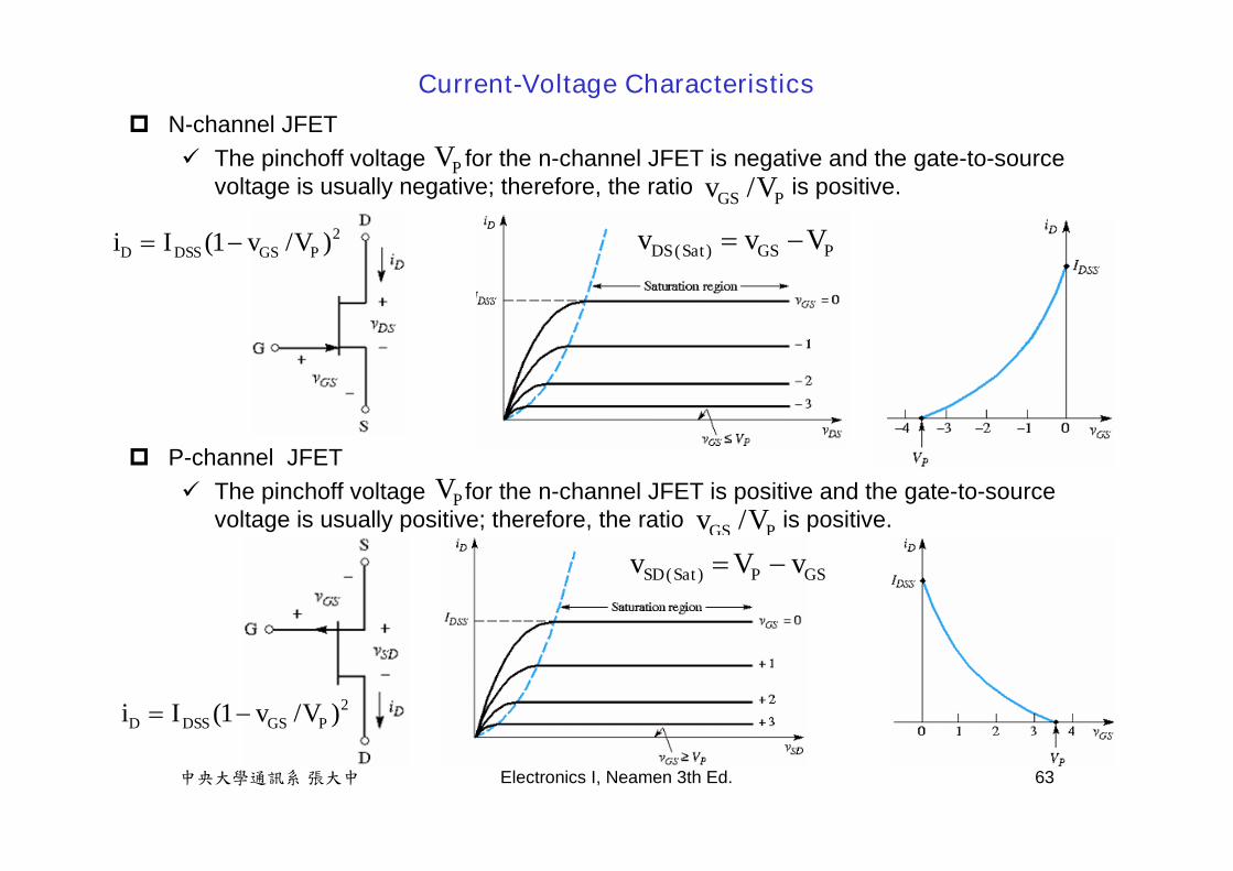
N-channel JFET The pinchoff voltage for the n-channel JFET is negative and the gate-to-source
voltage is usually negative; therefore, the ratio is positive.
P-channel JFET The pinchoff voltage for the n-channel JFET is positive and the gate-to-source
voltage is usually positive; therefore, the ratio is positive.
Current-Voltage Characteristics
PVPGS Vv /
2)/1( PGSDSSD VvIi PGSSatDS Vvv )(
PVPGS Vv /
2)/1( PGSDSSD VvIi
GSPSatSD vVv )(

中央大學通訊系 張大中 Electronics I, Neamen 3th Ed. 64

中央大學通訊系 張大中 Electronics I, Neamen 3th Ed. 65
Output Resistance for PN JFET
Saturation Region for Ideal Enhancement-mode MESFET
Nonsaturation Region for Ideal Enhancement-mode MESFET
JFET Properties
For an n-channel enhancement-mode MESFET, the threshold voltage is positive.
)1()/1( 2DSPGSDSSD vVvIi
112
const.
1
)/1(
DQPGSDSS
vDS
DO IVvI
vi
r
GS
2)( TNGSnD VvKi
])(2[ 2DSDSTNGSnD vvVvKi
中央大學通訊系 張大中 Electronics I, Neamen 3th Ed. 66

中央大學通訊系 張大中 Electronics I, Neamen 3th Ed. 67

中央大學通訊系 張大中 Electronics I, Neamen 3th Ed. 68

中央大學通訊系 張大中 Electronics I, Neamen 3th Ed. 69