Recommendations for board assembly of Infineon transistor ...
Upload
independentCategory
view
1download
0
ARTICLE IN PRESS
Physica E 41 (2008) 196–201
Contents lists available at ScienceDirect
Physica E
1386-94
doi:10.1
� Corr
E-m
journal homepage: www.elsevier.com/locate/physe
Impact of single halo implantation on the carbon nanotube field-effecttransistor: A quantum simulation study
Zahra Arefinia, Ali A. Orouji �
Electrical Engineering Department, Semnan University, Semnan, Iran
a r t i c l e i n f o
Article history:
Received 7 June 2008
Accepted 7 July 2008Available online 16 July 2008
PACS:
85.35.p
85.35.Kt
68.65.k
Keywords:
CNTFET
Short-channel effects (SCEs)
Single halo (SH) implantation
Non-equilibrium Green’s function (NEGF)
77/$ - see front matter & 2008 Elsevier B.V. A
016/j.physe.2008.07.003
esponding author. Tel.: +98 2614462954; fax
ail address: [email protected] (A.A. Orouji).
a b s t r a c t
For the first time, the impact of single halo (SH) implantation on the carbon nanotube field-effect
transistor (CNTFET) with doped source and drain extensions has been investigated using quantum
simulation. The simulations are based on the self-consistent solution of the two-dimensional
Poisson–Schrodinger equation, within the non-equilibrium Green’s function (NEGF) formalism. The
results show SH-CNTFET decreases significantly leakage current and drain conductance and increases
on–off current ratio and voltage gain as compared to conventional CNTFET. It is seen that short-channel
effects in this structure are suppressed because of the perceivable step in the surface potential profile,
which screens the drain potential.
& 2008 Elsevier B.V. All rights reserved.
1. Introduction
Carbon nanotube field-effect transistors (CNTFETs) are ultrathin body devices [1] that do not suffer from severe mobilitydegradation as typically observed for silicon MOSFETs withnanometer dimensions [2]. CNT transistors scaled down to�10 nm or even shorter have attracted a great deal of interest[3–5].
Archetype CNTFETs are currently planar in nature, mostly dueto their relative simplicity and moderate compatibility withexisting manufacturing technologies, but ultimate performanceis likely to be reached by employing a coaxial geometry [6].Coaxial structures are not easily realized in practice, but they havebeen the subject of several theoretical investigations that haveattempted to establish performance limits [4].
On the other hand, the control of the gate voltage on thechannel decreases as the channel length shrinks because of theincreased charge sharing from source and drain. Therefore, drain-induced barrier lowering (DIBL) is an important issue withdecreasing channel length that needs to be addressed whileproviding immunity against short-channel effects (SCEs). Toenhance the immunity against SCEs, several novel devicestructures have been reported in literature to circumvent the
ll rights reserved.
: +98 2313331623.
undesirable SCEs in MOSFETs [7,8]. Halo implantation is one of thedevice technologies to realize high performance [9,10]. Haloimplantation creates a non-uniform potential under the channeland causes to suppress channel leakage current [11].
In order to achieve the benefits of both halo implantation andCNTFET structures, we have proposed application of single halo(SH) implantation in CNTFET structures to reduce SCEs. Therefore,for the first time we have simulated SH-CNTFET structure usingtwo-dimensional (2-D) quantum simulation. The simulationshave been done by self-consistently solution between 2-D Poissonequation and Schrodinger equation with open boundary condi-tions, within the non-equilibrium Green’s function (NEGF) frame-work. Then we have obtained the fundamental electricalproperties of SH-CNTFET such as output characteristics, transcon-ductance characteristics, local density of states, electron density,electron velocity, and electrostatic potential of the conductionband. Our results demonstrate that the proposed SH-CNTFETexhibits significantly reduced short-channel effects thus makingit a more reliable device configuration than the conven-tional CNTFET (C-CNTFET) for high performance CMOS circuitapplications.
2. SH-CNTFET structure
In the SH-CNTFET, as shown in Fig. 1, we consider a (13, 0) CNTwith a diameter of �1 nm that is embedded in a cylindrical gate

ARTICLE IN PRESS
VG
VSVD
i-CNTn -CNT n -CNT
5 nm 30 nm 30 nm 10 nm
15 nm
2nm
p-CNT
z
r
b2q b2q b2q b2qtt
U1 U2 UN-1 UN
Halo implantation
t
Fig. 1. (a) SH-CNTFET structure with coaxial gate. Halo implantation with length of 5 nm on the source side of the SH-CNTFET is illustrated. (b) Mode-space Hamiltonian.
The circles and squares correspond to two nonequivalent real space carbon rings, A and B, respectively.
Z. Arefinia, A.A. Orouji / Physica E 41 (2008) 196–201 197
insulator of HfO2 with thickness 2 nm and dielectric constant 16[12]. The channel length is 15 nm, which consists of 10 nmundoped (intrinsic) CNT and 5 nm p-doped CNT as halo implanta-tion. The length of n-doped CNT extensions is 30 nm at the sourceand drain ends. Pocket implantation on the source side of the SH-CNTFET is kept at 0.7 nm�1 and the source/drain doping is 1 nm�1.All the device parameters of the C-CNTFET are equal to the SH-CNTFET unless its 15 nm channel is intrinsic CNT.
3. Simulation approach
Since the potential and charge density are invariant around thenanotube in the coaxially gated carbon nanotube transistor,the Poisson equation is essentially a 2-D problem along the tube(z-direction) and the radial direction (r-direction) in cylindricalcoordinates. Therefore, we obtain the self-consistent electrostaticsusing a 2-D finite difference method. The potential profile obeysthe Poisson equation
r2Ujðr; zÞ ¼ �
q
�rðr; zjÞ (1)
where Uj(r,z) is the electrostatic potential, e is the dielectricconstant, and r(r,zj) is the net charge density distribution, whichincludes dopant density as well. The net charge distribution r(r,zj)is given by
rðr ¼ rCNT; zjÞ ¼ pðzjÞ � nðzjÞ þ NþD � N�ArðrarCNT; zÞ ¼ 0 (2)
where rCNT is equal to CNT radius, ND+ and NA
� are the ionized donorand acceptor concentrations, respectively. Here, it is assumed thatthe induced charge and the dopants are uniformly distributedover the CNT surface. The electron and hole concentrations (n andp, respectively) are computed by solving the Schrodinger equationwith open boundary conditions by means of the NEGF formalism[13].
The retarded Green’s function for the device in matrix form iscomputed as [14]
GðEÞ ¼ ½ðEþ iZþÞI � H � SS � SD��1 (3)
where SS and SD are the self-energies of the source and drain,respectively, Z+ is an infinitesimal positive value, E is the energy,
I is the identity matrix, and H is the Hamiltonian of the CNT. Ascan be seen from Eq. (3), the transport is assumed here to becompletely ballistic.
The device Hamiltonian used in this paper is based on theatomistic nearest neighbor pz-orbital tight-binding approximation[15]. The cylindrical geometry of the device, which is shown inFig. 1(a), ensures symmetry in the angular direction, thusdrastically simplifying the mode-space treatment of electrontransport [16,17].
In the mode-space treatment of an (n, 0) zigzag CNT, thedependence of the electronic state on the angle along the tube’scircumference j is expanded in a set of circular harmonicsexp(iqj) with the angular quantum number q. It spans the integervalues of 1–2n or, equivalently, �n+1 to n. The integer values of q
outside this range would produce equivalent harmonics at thecrystal lattice sites. The total Hamiltonian splits into independentmatrices for subbands associated with each value of q [16], givingrise to a 1-D Hamiltonian with two-site unit cell, as schematicallyshown in Fig. 1(b), where each site corresponds to one of the twononequivalent real space carbon rings, A or B. The period of thezigzag tube in the longitudinal direction contains four such rings,ABAB, and has a length of 3acc [15], where acc ¼ 0.142 nm is thecarbon–carbon bond length in graphene.
The Hamiltonian matrix for the subbands with angularquantum number q in an (n, 0) zigzag CNT is then given by
H ¼
U1 b2q
b2q U2 t 0
t U3 b2q
. ..
0 t UN�1 b2q
b2q UN
266666666664
377777777775
N�N
(4)
where b2q ¼ 2t cos(pq/n), tE3 eV is the nearest neighbor hoppingparameter, and N is the total number of carbon rings along thedevice. Here, the diagonal elements Uj correspond to the on-siteelectrostatic potential along the tube surface. All electronicsubbands in a CNT are fourfold degenerate due to the two spinstates and the twofold valley degeneracy [15]. The valleydegeneracy comes from the two subbands with the same energydispersion but with different q-values.
ARTICLE IN PRESS
0 0.1 0.2 0.3 0.4 0.50
1
2
3
4
5
6
Dra
in C
urre
nt (µ
A)
Drain-Source Voltage (V)
SH-CNTFETC-CNTFET
VGS=0.5 V
Fig. 2. Output characteristics of C-CNTFET and SH-CNTFET structures at VGS ¼ 0.5 V.
Z. Arefinia, A.A. Orouji / Physica E 41 (2008) 196–201198
Particular attention must be put in the definition of each self-energy matrix, which can be interpreted as a boundary conditionof the Schrodinger equation. In our simulation, we haveconsidered a self-energy for semi-infinite leads as boundaryconditions, which enables to consider the CNT as connected toinfinitely long CNTs at its ends. The source self-energy function SS
has all its entries zero except for the (1,1) element [16]:
SSð1;1Þ
¼ðE� U1Þ
2þ t2 þ b2
2q �
ffiffiffiffiffiffiffiffiffiffiffiffiffiffiffiffiffiffiffiffiffiffiffiffiffiffiffiffiffiffiffiffiffiffiffiffiffiffiffiffiffiffiffiffiffiffiffiffiffiffiffiffiffiffiffiffiffiffiffiffiffiffiffiffiffiffiffiffiffiffiffiffiffiffiffiffiffiffiffiffi½ðE� U1Þ
2þ t2 þ b2
2q�2 � 4ðE� U1Þ
2t2q
2ðE� U1Þ
(5)
Similarly, SD has only its (N, N) element nonzero, and it is given byan equation similar to Eq. (5) with U1 replaced by UN.
Level broadening can be defined as follows [18]:
GðEÞ ¼ i SðEÞ �SyðEÞj k
¼ SinðEÞ þ Sout
ðEÞ (6)
where Sy represents the Hermitean conjugate of S matrix. Also,Sin/out are the in/out-scattering functions for contact coupling,which defined as below
SinS=D ¼ GS=Df E� EFS=FD
� �(7a)
SoutS=D ¼ GS=D½1� f ðE� EFS=FDÞ� (7b)
where f(E) is the Fermi distribution, and EFS/FD denotes the sourceand drain Fermi energies, respectively. The electron and holecorrelation functions are then given by
GnðEÞ ¼ GðEÞSin
ðEÞGyðEÞ (8a)
GpðEÞ ¼ GðEÞSout
ðEÞGyðEÞ (8b)
Note that the electron and hole correlation functions Gn=pi=j ðE; qÞ
are the matrices defined in the basis set of ring numbers i, j andsubbands q (we will imply the last index in the rest of this paper).Thus, the diagonal elements of Gn=p
i=j ðE; qÞ correspond to the energydensity of carrier occupation at those basis sites (single carbonring, A or B, in a specific subband) with a given energy E.Therefore, the total electron/hole density (per unit length) at a sitezj is given by
nðzjÞ ¼Xq;s
1
Dz
Z þ1�1
Gnj;jðE; qÞ
2pdE (9a)
pðzjÞ ¼Xq;s
Z þ1�1
Gpj;jðE;qÞ
2p dE1
Dz(9b)
where summation is performed over the spin and subbandvariables, and it produces the degeneracy factor of four (for eachnonequivalent subband).
It should be noted that, even though Eqs. (9a) and (9b) give thetotal carrier densities distributed throughout the whole energyrange, what we really need in determining the self-consistentpotential on the tube surface, Uj�U(r ¼ rCNT, zj), is the inducedcharge density. This can be determined by performing theintegrals in Eqs. (9a) and (9b) in a limited energy range definedwith respect to the local charge neutrality energy EN [19,20]. In asemiconducting CNT, due to the symmetry of the conduction andvalence bands, EN is expected to be at the midgap energy.Therefore, the induced electron and hole densities at site zj,which are calculated from Eqs. (9a) and (9b), are
nðzjÞ ¼4
Dz
Z þ1EN ðjÞ
Gnj;jðEÞ
2pdE (10a)
pðzjÞ ¼4
Dz
Z EN ðjÞ
�1
Gpj;jðEÞ
2pdE (10b)
Finally, the Poisson equation is solved to determine the self-consistent electrostatic potential Uj along the tube surface. Thecalculated potential Uj
new gives rise to a modified Hamiltonian(Eq. (4)), eventually leading to the self-consistent loop betweenthe electrostatics and the quantum transport. The convergencecriterion is used in this process to monitor the maximum changein the potential profile between consecutive iterations, i.e., max(|Uj
old�Uj
new|) pUtol, where the tolerance value Utol is normallytaken to be 1 meV.
Finally, the current flow from site zj to zj+1 in the nearestneighbor tight-binding scheme can be expressed as [21]
Ij!jþ1 ¼Xq;s
ie
_
Z þ1�1
dE
2p ½Hj;jþ1ðqÞGnjþ1;jðE; qÞ � Hjþ1;jðqÞG
nj;jþ1ðE; qÞ�
(11)
wherein the nondiagonal terms of the Hamiltonian (Eq. (4))contain only the contributions of hopping. It is worth mentioningthat the aforementioned equation is a general relationship that isvalid even under dissipative transport. Under ballistic conditions,however, Eq. (11) further simplifies (for each nonequivalentsubband) to
I ¼4e
_
Z þ1�1
dE
2p TðEÞ½f ðE� EFSÞ � f ðE� EFDÞ� (12)
with the transmission coefficient T(E) given by
TðEÞ ¼ traceðGSðEÞGðEÞGDðEÞGyðEÞÞ (13)
From a numerical point of view, Green’s function is computedby means of the recursive Green’s function (RGF) technique[21,22].
4. Results and discussion
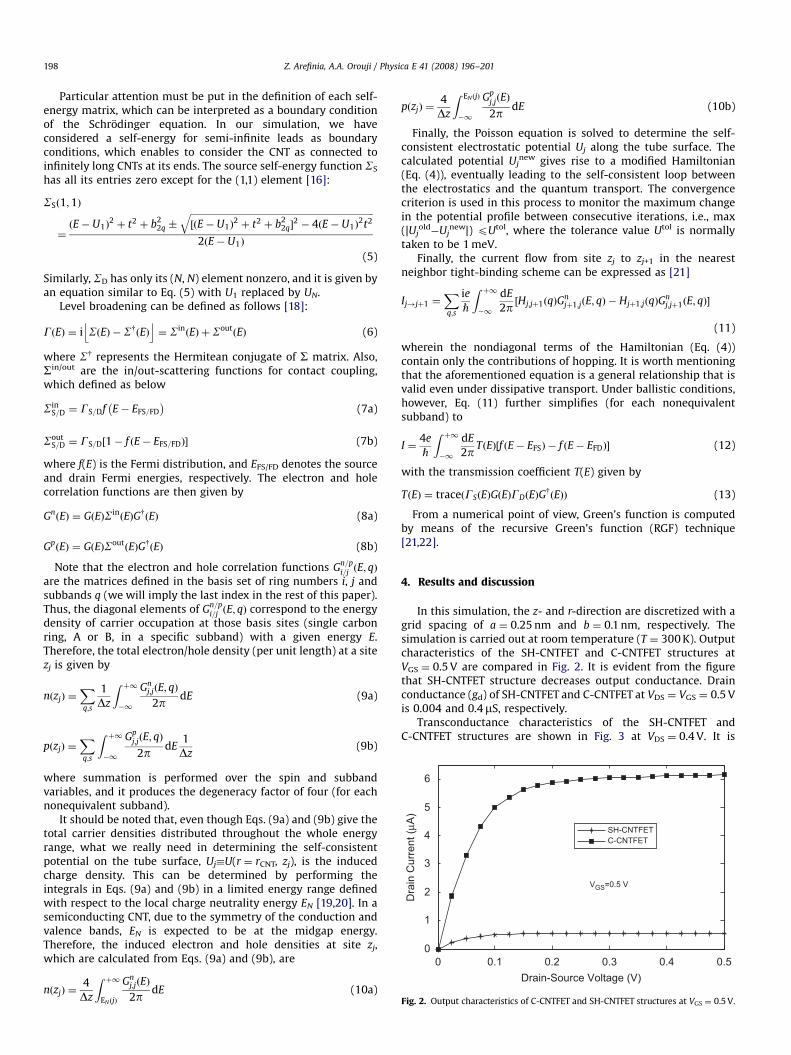
In this simulation, the z- and r-direction are discretized with agrid spacing of a ¼ 0.25 nm and b ¼ 0.1 nm, respectively. Thesimulation is carried out at room temperature (T ¼ 300 K). Outputcharacteristics of the SH-CNTFET and C-CNTFET structures atVGS ¼ 0.5 V are compared in Fig. 2. It is evident from the figurethat SH-CNTFET structure decreases output conductance. Drainconductance (gd) of SH-CNTFET and C-CNTFET at VDS ¼ VGS ¼ 0.5 Vis 0.004 and 0.4mS, respectively.
Transconductance characteristics of the SH-CNTFET andC-CNTFET structures are shown in Fig. 3 at VDS ¼ 0.4 V. It is
ARTICLE IN PRESS
0 0.2 0.4 0.6 0.8 110-8
10-710-6
10-510-410-3
10-210-1
100101
Dra
in C
urre
nt (µ
A)
Gate-Source Voltage (V)
SH-CNTFETC-CNTFET
VDS=0.4V
Fig. 3. Transconductance characteristics of C-CNTFET and SH-CNTFET structures
on logarithmic scale at VDS ¼ 0.4 V.
0 0.2 0.4 0.6 0.8 1
10
20
30
40
50
60
Gate-Source Voltage (V)
Dra
in C
urre
nt (µ
A)
SH-CNTFETC-CNTFET
VDS=0.4V
VDS=40mV
Fig. 4. Transconductance characteristics of C-CNTFET and SH-CNTFET structures
on linear scale at VDS ¼ 0.4 V and VDS ¼ 40 mV.
0 1 3 5 7 9 11 13 15
-0.1
0
0.1
0.2
0.3
Position along the Channel (nm)
Pot
entia
l (V
)
SH-CNTFETC-CNTFET
VGS=0.5 VVDS=0.4V
Fig. 5. Potential profile along the channel of SH-CNTFET and C-CNTFET at
VGS ¼ 0.5 V and VDS ¼ 0.4 V.
Fig. 6. Electrostatic potential of conduction band of nanotube as a function of
drain-source voltage (VDS) and position along the nanotube at VGS ¼ 0.5 V.
Z. Arefinia, A.A. Orouji / Physica E 41 (2008) 196–201 199
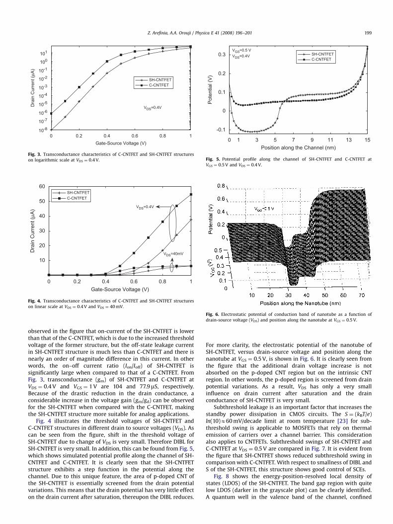
observed in the figure that on-current of the SH-CNTFET is lowerthan that of the C-CNTFET, which is due to the increased thresholdvoltage of the former structure, but the off-state leakage currentin SH-CNTFET structure is much less than C-CNTFET and there isnearly an order of magnitude difference in this current. In otherwords, the on–off current ratio (Ion/Ioff) of SH-CNTFET issignificantly large when compared to that of a C-CNTFET. FromFig. 3, transconductance (gm) of SH-CNTFET and C-CNTFET atVDS ¼ 0.4 V and VGS ¼ 1 V are 104 and 77.9mS, respectively.Because of the drastic reduction in the drain conductance, aconsiderable increase in the voltage gain (gm/gd) can be observedfor the SH-CNTFET when compared with the C-CNTFET, makingthe SH-CNTFET structure more suitable for analog applications.
Fig. 4 illustrates the threshold voltages of SH-CNTFET andC-CNTFET structures in different drain to source voltages (VDS). Ascan be seen from the figure, shift in the threshold voltage ofSH-CNTFET due to change of VDS is very small. Therefore DIBL forSH-CNTFET is very small. In addition, this can be found from Fig. 5,which shows simulated potential profile along the channel of SH-CNTFET and C-CNTFET. It is clearly seen that the SH-CNTFETstructure exhibits a step function in the potential along thechannel. Due to this unique feature, the area of p-doped CNT ofthe SH-CNTFET is essentially screened from the drain potentialvariations. This means that the drain potential has very little effecton the drain current after saturation, thereupon the DIBL reduces.
For more clarity, the electrostatic potential of the nanotube ofSH-CNTFET, versus drain-source voltage and position along thenanotube at VGS ¼ 0.5 V, is shown in Fig. 6. It is clearly seen fromthe figure that the additional drain voltage increase is notabsorbed on the p-doped CNT region but on the intrinsic CNTregion. In other words, the p-doped region is screened from drainpotential variations. As a result, VDS has only a very smallinfluence on drain current after saturation and the drainconductance of SH-CNTFET is very small.
Subthreshold leakage is an important factor that increases thestandby power dissipation in CMOS circuits. The S ¼ (kBT/e)ln(10)E60 mV/decade limit at room temperature [23] for sub-threshold swing is applicable to MOSFETs that rely on thermalemission of carriers over a channel barrier. This considerationalso applies to CNTFETs. Subthreshold swings of SH-CNTFET andC-CNTFET at VDS ¼ 0.5 V are compared in Fig. 7. It is evident fromthe figure that SH-CNTFET shows reduced subthreshold swing incomparison with C-CNTFET. With respect to smallness of DIBL andS of the SH-CNTFET, this structure shows good control of SCEs.
Fig. 8 shows the energy-position-resolved local density ofstates (LDOS) of the SH-CNTFET. The band gap region with quitelow LDOS (darker in the grayscale plot) can be clearly identified.A quantum well in the valence band of the channel, confined
ARTICLE IN PRESS
Z. Arefinia, A.A. Orouji / Physica E 41 (2008) 196–201200
states in it and tunneling from valence well into band gap can beseen. Because of the existence of the barriers at the source anddrain end, the source/drain incident wave is reflected and thequantum interference pattern between the incident and reflectedwaves is apparent.
Fig. 8. Energy-position-resolved local density of states (LDOS) for SH-CNTFET at
VGS ¼ 0.1 V and VDS ¼ 0.5 V. Also energy profile of conduction (EC) and valence (EV)
band, source Fermi level (EFS) and drain Fermi level (EFD) are depicted.
0 1 3 5 7 9 11 13 15
-4
-3
-2
-1
0
1
2
x 106
Position along the Channel (nm)
Ele
ctro
n D
ensi
ty (c
m-1
)
VDS=0.4 V
p-CNT i-CNT
VGS=0 V
VGS=0.1 V
VGS=0.2 V
VGS=0.3 V
VGS=0.4 V
Fig. 9. Charge distribution of the SH-CNTFET along the channel for different gate-
source biases at VDS ¼ 0.4 V.
0.1 0.2 0.3 0.4 0.5 0.6 0.7
60
500
1000
Gate-Source Voltage (V)
Sw
ing
(mV
/dec
ade)
SH-CNTFETC-CNTFET
VDS=0.5 V
Fig. 7. Subthreshold swing of SH-CNTFET and C-CNTFET at VDS ¼ 0.5 V.
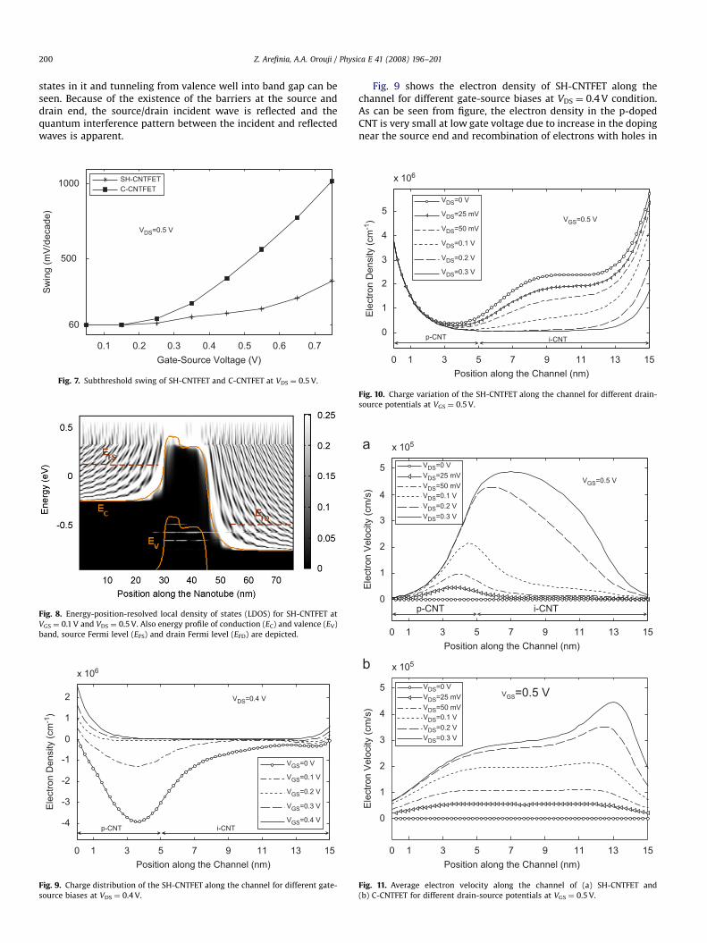
Fig. 9 shows the electron density of SH-CNTFET along thechannel for different gate-source biases at VDS ¼ 0.4 V condition.As can be seen from figure, the electron density in the p-dopedCNT is very small at low gate voltage due to increase in the dopingnear the source end and recombination of electrons with holes in
0 1 3 5 7 9 11 13 15
0
1
2
3
4
5
x 106
Position along the Channel (nm)E
lect
ron
Den
sity
(cm
-1)
VDS=0 V
VDS=25 mV
VDS=50 mV
VDS=0.1 V
VDS=0.2 V
VDS=0.3 V
p-CNT i-CNT
VGS=0.5 V
Fig. 10. Charge variation of the SH-CNTFET along the channel for different drain-
source potentials at VGS ¼ 0.5 V.
0 1 3 5 7 9 11 13 15
0
1
2
3
4
5
x 105
Position along the Channel (nm)
Ele
ctro
n V
eloc
ity (c
m/s
)
p-CNT
VDS=0 VVDS=25 mVVDS=50 mVVDS=0.1 VVDS=0.2 VVDS=0.3 V
i-CNT
VGS=0.5 V
0 1 3 5 7 9 11 13 15
0
1
2
3
4
5
x 105
Position along the Channel (nm)
Ele
ctro
n V
eloc
ity (c
m/s
)
VGS=0.5 VVDS=0 VVDS=25 mVVDS=50 mVVDS=0.1 VVDS=0.2 VVDS=0.3 V
Fig. 11. Average electron velocity along the channel of (a) SH-CNTFET and
(b) C-CNTFET for different drain-source potentials at VGS ¼ 0.5 V.
ARTICLE IN PRESS
Z. Arefinia, A.A. Orouji / Physica E 41 (2008) 196–201 201
this region. The surface electron density profile of SH-CNTFETalong the channel at different drain-source potential is shown inFig. 10. It is clearly seen that variation of electron density withdrain-source potential in the p-doped channel region is verysmall. So halo implantation is caused by reduction of electrondensity in the channel. Consequently, decreasing of electrondensity reduces mobility.
Figs. 11(a) and (b) show simulated value of electron velocityalong the channel for SH-CNTFET and C-CNTFET, respectively.These clearly show that velocity peaks of C-CNTFET are near thedrain end, while velocity peaks of SH-CNTFET are far from drainend, in the vicinity of the halo pocket. Also, there is a considerablereduction in the velocity at the drain end in the case of the SH-CNTFET structure when compared with C-CNTFET. Therefore, weare expecting that the hot carrier effect improves with theelectron velocity reduction at the drain end of SH-CNTFET [24].
5. Conclusion
In this paper, a two-dimensional (2-D) full quantum mechan-ical simulation has been developed to evaluate the fundamentalphysics of application of single halo (SH) implantation to thecarbon nanotube field-effect transistor (CNTFET) with dopedsource and drain. The simulation loop consists of two blocks:the Poisson equation, which is solved for the potential profile, andthe transport equation, which is solved for charge and currentdistribution in the device. The ballistic transport is modeled bySchrodinger equation. The Schrodinger equation is solved usingthe well-known non-equilibrium Green’s function technique. Thefinite difference discretization scheme is used in all of thenumerical implementation. The results have shown SH-CNTFETdecreases significantly leakage current and increases on–offcurrent ratio as compared to C-CNTFET. Also, there is draincurrent reduction in the SH-CNTFET that results from thethreshold voltage increment and the mobility reduction. Conse-
quently, because of the drastic reduction in the drain conductanceof SH-CNTFET, a considerable increase in the voltage gain can beobserved for the SH-CNTFET when compared with the C-CNTFET.From the device point of view, SH-CNTFET structure shows bettercontrol of SCEs and makes it suitable for high-performance CMOSapplications.
References
[1] J. Appenzeller, J. Knoch, R. Martel, V. Derycke, S. Wind, P. Avouris, IEEE Trans.Nanotechnology 1 (2002) 184.
[2] K. Uchida, J. Koga, S. Takagi, IEDM Tech. Dig. (2003) 805.[3] F. Leonard, J. Tersoff, Phys. Rev. Lett. 88 (2002) 258302.[4] J. Guo, M. Lundstrom, S. Datta, Appl. Phys. Lett. 80 (2002) 3192.[5] T.S. Xia, L.F. Register, S.K. Banerjee, J. Appl. Phys. 95 (2004) 1597.[6] J. Guo, S. Goasguen, M. Lundstrom, S. Datta, Appl. Phys. Lett. 81 (2002)
1486.[7] A. Chaudhry, M.J. Kumar, IEEE Trans. Device Mater. Reliab. 4 (2004) 99.[8] A.A. Orouji, M.J. Kumar, IEEE Trans. Device Mater. Reliab. 5 (2005) 509.[9] G.V. Reddy, M.J. Kumar, Microelectron. J. 35 (2004) 761.
[10] S. Zanchetta, A. Todon, A. Abramo, L. Selmi, E. Sangiorgi, Solid-State Electron.46 (2002) 429.
[11] T. Endoh, Y. Momma, IEICE TRANS. ELECTRON. E 90-C (2007) 1000.[12] Z. Arefinia, A.A. Orouji, Physica E (2008), doi:10.1016/j.physe.2008.04.005.[13] S. Datta, Superlattices Microstruct. 28 (2000) 253.[14] S. Datta, Electronic Transport in Mesoscopic Systems, Cambridge University
Press, Cambridge, UK, 1995.[15] R. Saito, G. Dresselhaus, M.S. Dresselhaus, Physical Property of Carbon
Nanotubes, Imperial College Press, London, UK, 1998.[16] J. Guo, S. Datta, M. Lundstrom, M.P. Anantram, Int. J. Multiscale Comput. Eng.
2 (2004) 257.[17] R. Venugopal, Z. Ren, S. Datta, M.S. Lundstrom, D. Jovanovic, J. Appl. Phys. 92
(2002) 3730.[18] S. Datta, Quantum Transport: Atom to Transistor, Cambridge University. Press,
Cambridge, UK, 2005.[19] J. Tersoff, Phys. Rev. Lett. 52 (1984) 465.[20] J. Tersoff, Phys. Rev. Lett. 56 (1986) 675.[21] R. Lake, G. Klimeck, R.C. Bowen, D. Jovanovic, J. Appl. Phys. 81 (1997) 7845.[22] A. Svizhenko, M.P. Anantram, T.R. Govindam, B. Biegel, J. Appl. Phys. 91 (2001)
2343.[23] S.M. Sze, Physics of Semiconductor Devices, Wiley, New York, 1981.[24] T.H. Ning, P.W. Cook, R.H. Dennard, C.M. Schuster, H.N. Yu, IEEE Trans.
Electron Devices ED-26 (1979) 346.
Copyright © 2022 FDOKUMEN