Spin valve transistor (Spintronics)
26
A SEMINAR REPORT ON SPIN VALVE TRANSISTOR Seminar In charge Seminar Guide Submitted By Er. Amit Katiyar Er. Ajeet Srivastava Eeshan Mishra Er. Roli Nigam University Institute of Engineering & Technology Chhatrapati Sahu Ji Maharaj University Kanpur-208024 Session 2013-2014
-
Upload
kanpuruniversity -
Category
Documents
-
view
8 -
download
0
Transcript of Spin valve transistor (Spintronics)

A
SEMINAR REPORT
ON
SPIN VALVE TRANSISTOR
Seminar In charge Seminar Guide Submitted By
Er. Amit Katiyar Er. Ajeet Srivastava Eeshan Mishra
Er. Roli Nigam
University Institute of Engineering & Technology
Chhatrapati Sahu Ji Maharaj University
Kanpur-208024
Session 2013-2014

CONTENTS
1. INTRODUCTION……………………………………………………………………….……..1
2. BASIC DEVICE STRUCTURE AND PROPERTIES…………………………….………. …6
3. FABRICATION: VACUUM METAL BONDING………………………………………..….11
4. PHYSICAL BASIS: HOT ELECTRON SPIN TRANSPORT……………………………….14
5. (MAGNETORESISTIVE RANDOM ACCESS MEMORY (MRAM)…………….………..16
6. ADVANTAGES OF SPIN VALVE TRANSISTOR…………………………………………20
7. LIMITATIONS OF SPIN VALVE TRANSISTOR …………………………………….……20
8. APPLICATIONS OF SPIN VALVE TRANSIATOR…………………………………….…21
9. CONCLUSIONS………………………………………………………………..………..…...22
10. REFERENCES………………………………………………………………………………23

LIST OF FIGURES
1. Scheme of Electronics using spin degrees of freedom……………………………………1
2. Ways in which semiconductor and ferromagnetic material can be combined…….………3
3. Basic layout of SVT…………………………………………………………………...…..6
4. Energy Band diagram of SVT…………………..…………………………………………7
5. Collector current v/s magnetic field………………………………….......………………..8
6. Collector current v/s collector base voltage……………………………..……………….09
7. Concept of Vacuum metal bonding…………………………………….………………..11
8. Final test chip with 52 SVTs…………………………………………………..…………13
9. MRAM introduced………………………………………………………….……...…....16
10. MRAM reading process…………………………………………………………………17
11. MRAM writing process…………………………………………………………………17
12. MRAM v/s Other technologies………………………………………………………..…18
13. Thermally assisted magnetic switching………………………………………….………19

ABSTRACT
In a world of ubiquitous presence of electrons can you imagine any other field displacing
it? It may seem peculiar, even absurd, but with the advent of spintronics it is turning into reality.
In our conventional electronic devices we use semi conducting materials for logical
operation and magnetic materials for storage, but spintronics uses magnetic materials for both
purposes. These spintronic devices are more versatile and faster than the present one. One such
device is Spin Valve Transistors (SVT).
Spin valve transistor is different from conventional transistor. In this for conduction we
use spin polarization of electrons. Only electrons with correct spin polarization can travel
successfully through the device. These transistors are used in data storage, signal processing,
automation and robotics with less power consumption and results in less heat. This also finds its
application in Quantum computing, in which we use Qubits instead of bits.

INTRODUCTION
Fig 0: Scheme of Electronics using spin degrees of freedom
Two experiments in 1920‟s suggested spin as an additional property of the electron. One
was the closely spaced splitting of Hydrogen spectral lines, called fine structure. The other was
Stern – Gerlach experiment, which in 1922 showed that a beam of silver atoms directed through
an inhomogeneous magnetic field would be forced in to two beams. These pointed towards
magnetism associated with the electrons.

Spintronics, also known as magneto electronics, manipulates the electron spin and resulting
magnetic moment, to achieve improved functionalities e.g. Spin transistors, memories, etc.
Spin is the root cause of magnetism that makes an electron tiny magnet. Magnetism is
already been exploited in recording devices. Where data is recorded and stored as tiny areas of
magnetized iron or chromium oxide. To access that information the head detects the minute
changes in magnetic field. This induces corresponding changes in the head‟s electrical resistance
– a phenomenon called Magneto Resistance.
BRIEF HISTORY
It seems almost inevitable that electronics in the near future will employ the electron spin
degree of freedom. Two exciting scientific breakthroughs within the last 15 years and their
exceptionally rapid implementation into products already demonstrate the impact of using the
electron spin. In 1988, the giant magneto resistance (GMR) effect was discovered in multilayer
structures that contain layers of ferromagnetic metals separated by a thin spacer of normal metal.
The resistance of such structures was found to depend greatly on the relative magnetic
1920s: Spin concept
1921 : Stern-Gerlach Experiment
The Moore's Law
1988: Discovery of Giant Magnetoresistance
1991: Invention of Spin Valve by IBM
1994: Magnetic Tunnel Junction with large Magneto resistance ratio
2002: Plastic Shows promise for SpintronicsMagnetic AComputer memory
2005: Commercialization of MTJ Read head

orientation of neighbouring magnetic layers, making it attractive for application in highly
sensitive magnetic field sensors.
As early as 1997, GMR was incorporated into the read-heads of magnetic hard disc
recording systems, where it has been one of the main factors enabling the tremendous increase in
storage density over the past decade. The second important breakthrough was the demonstration
in 1995 of large tunnel magneto resistance (TMR) in tunnel junctions in which two
ferromagnetic electrodes are separated by an ultrathin insulator.
Key features are the large spin dependence of the tunneling process, even at room
temperature, and the reproducible fabrication of reliable tunnel barriers typically using 1–2 nm of
Al2O3. These features facilitated the development of a high performance magnetic random access
memory (MRAM). It is non-volatile, has low power consumption and fast switching speed, and
has the potential of becoming a universal memory. The first introduction of tunneling based
MRAM into the market is imminent. While GMR and tunneling magneto resistance demonstrate
the opportunities of using electron spin, it is still an open question how pervasive the use of spin
will be, and what classes of material it will involve.
In GMR and TMR structures, Ferro magnets are combined with thin layers of normal
metals and insulators, respectively. We are thus missing the most essential material in
contemporary electronics, namely, semiconductors. The core element of electronics is the
transistor with its amplification, which relies on extremely pure semiconductor materials in
which electrical conduction can be controlled by manipulating the carrier density using electric
fields supplied by a gate. Semiconductors allow precise tuning of carrier concentrations, band
gap engineering, and, interestingly, also exhibit extremely long electron spin lifetimes , Spin-
electronics (or spintronics) based on semiconductors is therefore an active and promising
research field, with several approaches being explored in parallel. These are briefly reviewed
below. Spin-transport in (quantum-) structures built exclusively from non-magnetic or
paramagnetic semiconductors is explored actively, but a concern is that the creation of a spin
polarization at present involves optical techniques or large magnetic fields to induce a sizable
Zeeman splitting of the spin states. It would be advantageous to use conventional magnetic
materials such as Fe, Ni, Co and their alloys, in which ferromagnetism is robust and Curie
temperatures are high. This supports a stable, virtually ever lasting memory function, while
switching between different magnetization states is extremely rapid, typically at nanosecond or
even picosecond timescales. It is, thus, attractive to examine different ways (figure 1) to combine
ferromagnets and semiconductors.
The most straightforward approach is the one employed in MRAM, where an array of
magnetic memory elements is placed on top of a semiconductor wafer containing transistors and
other circuitry required to drive the memory.
This requires a modest, yet not trivial integration at the system level, but does not take
advantage of the unique properties of semiconductors in manipulating spin. The most intimate
form of integration is to put magnetic properties into semiconductor materials, thus creating
ferromagnetic semiconductors.
Such materials can be obtained by doping with a certain amount of magnetic atoms, as in
the case of the notable example of GaMnAs. Interplay between ferromagnetism and carrier
densities via electrical gating has been achieved in some of the materials. The hunt is now on for
compounds that exhibit both semiconducting and ferromagnetic properties at temperatures well
above room temperature.
An intermediate option is to create hybrid device structures in which ferromagnets and
semiconductors are combined. One could think of much different geometry of such hybrid
structures. Two main categories will be distinguished, based on whether the control and
manipulation of the spins occurs in the semiconductor or in the ferromagnetic material. In the
first category, electron spins that originate from a ferromagnetic source material are injected into
a semiconductor, in which they are transported and manipulated, followed by some means of
spin detection at the „other end‟ of the device. Much progress has recently been made on the first
important step of spin-injection into the semiconductor , but implementation into working
devices that operate at room temperature remains to be demonstrated. The opposite is true for the
second class of hybrid devices, where a device concept has been successfully demonstrated by
Monsma et al with the introduction of the spin-valve transistor (SVT) in 1995, and the
subsequent observation of huge magnetic response at room temperature a few years later. While
the spin dependence of the transport is in the ferromagnetic materials, the semiconductors are
used to create energy barriers in the electron‟s potential landscape that are essential to the
operation of the device.

BASIC DEVICE STRUCTURE AND PROPERTIES
The SVT was introduced in 1995 and is the first working hybrid device in which
ferromagnets and semiconductors have been closely integrated, and both materials are essential
in controlling the electrical transport through the device. The three-terminal device has the
typical emitter/base/collector structure of a (bipolar) transistor, but is different in that the base
region is metallic and contains at least two magnetic layers separated by a normal metal spacer
(see figure 2).

The two magnetic layers act as polarizer and analyzer of electron spins, such that the
relative orientation of the magnetization of the two layers determines the transmission of the
base. The resulting salient feature of the SVT is that the collector current depends on the
magnetic state of the base. This was first demonstrated by Monsma et al in a SVT showing a
huge change of 390% of the collector current in an applied magnetic field at low temperature. In
1998, the first device operating at room temperature was achieved, having a 15% effect in fields
of a few kOe. More recently, we succeeded in the reproducible fabrication of SVTs that exhibit
magneto current effects up to 400% at room temperature, and in small magnetic fields of only a
fewOe.
Unlike other spintronic devices, the SVT is based on the spin-dependent transport of non-
equilibrium, so-called hot electrons, rather than Fermi electrons. In order to illustrate this and
explain the principle of operation, let us consider the specific structure that was used. That

particular SVT uses silicon as the semiconductor for the emitter and collector, and has a metallic
base that contains a Ni80Fe20/Au/Co spin valve (see figure 3). At the interfaces between the metal
base and the semiconductors, energy barriers (Schottky barriers) are formed.
These energy barriers prevent electrons with the Fermi energy from travelling through the
structure. To obtain the desired high quality Schottky barrier with good rectifying behaviour and
thermionic emission dominating, low doped Si (1–10_cm) is used and thin layers of, e.g. Pt and
Au are incorporated at the emitter and collector side, respectively.
These also serve to separate the magnetic layers from direct contact with Si.The operation
of the SVT is as follows. A current is established between the emitter and the base (the emitter
current IE), such that electrons are injected into the base, perpendicular to the layers of the spin
valve. Since the injected electrons have to go over the Si/Pt Schottky barrier, they enter the base
as non-equilibrium, hot electrons. The hot electron energy is determined by the emitter Schottky,
which is typically between 0.5 and 1 eV, depending on the metal/semiconductor combination
[25]. As the hot electrons traverse the base, they are subjected to inelastic and elastic scattering,
which changes their energy as well as their momentum distribution. Electrons are only able to
enter the collector if they have
retained sufficient energy to
overcome the energy barrier at
the collector side, which is
chosen to be somewhat lower
than the emitter barrier.
Equally important, a hot
electron can only enter the
collector if its momentum
matches with that of one of the
available states in the collector
semiconductor. The fraction of
electrons that is collected, and thus the collector current IC, depends sensitively on the scattering
in the base, which is spin dependent when the base contains magnetic materials. The total
scattering rate is controlled with an external applied magnetic field, which changes the relative
magnetic alignment of the ferromagnetic Ni80Fe20 and Co layers in the base.
This is illustrated in figure 4, where IC at room temperature is plotted as a function of
magnetic field, for a transistor with a Si(100) emitter, a Si(111) collector and the following base:
Pt(20 Å)/NiFe(30 Å)/Au(35 Å)/Co(30 Å)/Au(20+20 Å).
At large applied fields, the two magnetic layers have their magnetization directions
aligned parallel. This gives the largest collector current (IP
C =11.2nA). When the magnetic field
is reversed, the difference in switching fields of Co(22 Oe) and NiFe (5 Oe) creates a field region
where the NiFe and Co magnetizations are antiparallel. In this state, the collector current is
drastically reduced (IAP
C = 3.3 nA). The magnetic response of the SVT, called the magneto
current (MC), is defined as the change in collector current normalized to the minimum value, i.e.
where P and AP refer to the
parallel and antiparallel
magnetic state of the base
spin valve, respectively.
Thus, the relative magnetic
response is MC = 240%,
which is huge indeed. It was
shown that the collector
current and the MC are
virtually independent of a
reverse bias voltage applied
across the collector Schottky
barrier, provided that the
intrinsic „leakage‟ current

this induces in the collector diode is negligible compared to the hot-electron current. This is
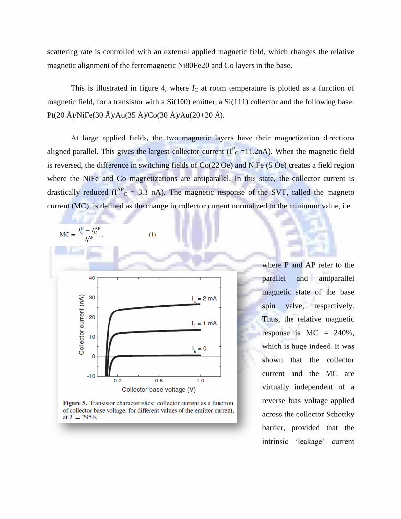
indeed the case, as can be seen in figure 5.
A voltage between base and collector does not affect the hot-electron current because it
does not significantly change the maximum of the Schottky barrier when measured with respect
to the Fermi energy in the metal. In other words, the energy barrier seen by hot electrons coming
from the base is hardly changed. Similarly, a change of the emitter to base voltage, or
equivalently the emitter current, does not affect the energy at which hot electrons are injected
into the base. Also here, the applied voltage hardly modifies the maximum of the emitter
potential barrier. The result is that the collector current is simply linearly proportional to the
emitter current, as shown in figure 6. It should be noted here that huge or even colossal magnetic
response has been observed in other materials and devices. The uniqueness of the SVT is that the
huge relative magnetic effect is obtained at room temperature, and that only small magnetic
fields of a few Oe are required. The combination of these three features is what makes it
attractive. Furthermore, the results are reproducible and the properties of the device can be
manipulated to a certain extent by controlling the thickness of layers, the type of materials, etc.
Nevertheless, a particular point that needs attention is the absolute value of the output current. In
the above example, an emitter current of 2mA was used and the corresponding transfer ratio,
defined as α = IC/IE, is thus of the order of 10−6
. In this context, it is important to remember that
the term „transistor‟ should not be confused with „amplifier‟. The word transistor was chosen in
analogy with the metal base transistor (MBT), a device that is similar to the SVT except that the
base contains only non-magnetic metals. These structures were studied extensively in the 1960s
and 1970s, from which it became clear that a metallic base has too little transmission to support
amplification, Hence, the SVT should not be judged on its (lack of) amplification. Rather, it
should be viewed as a device with a magnetic field dependent electrical output, which is the
basic functionality one needs for a magnetic field sensor or a magnetic memory element.
Although current gain is thus not required for most applications, a small absolute current is a
disadvantage. This issue and the progress made so far is addressed in one of the subsequent
sections.
The energy barrier at the emitter side is needed to create injection of hot electrons, such
that transport is governed by non-equilibrium processes. The collector energy barrier acts as an
energy and momentum filter, allowing only a fraction of the hot electrons to pass into the
collector, and reflecting the rest. The collector Schottky barrier (Au/Si in the above example)
selects only on the basis of energy and momentum, but not on the spin of the incoming hot
electrons. In some sense, the role of spin is thus indirect as it is merely used to manipulate the
energy and momentum distribution of the hot electrons during their motion through the base.
This is essential though, as spin couples to an external applied magnetic field and is our handle to
the outside world. The origin of the large magnetic sensitivity of the SVT is the non-equilibrium
nature of the transport that gives an exponential decay of base transmission, together with the
strong spin dependence of the elastic and inelastic scattering parameters in ferromagnetic
materials.
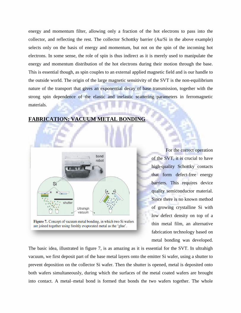
FABRICATION: VACUUM METAL BONDING
For the correct operation
of the SVT, it is crucial to have
high-quality Schottky contacts
that form defect-free energy
barriers. This requires device
quality semiconductor material.
Since there is no known method
of growing crystalline Si with
low defect density on top of a
thin metal film, an alternative
fabrication technology based on
metal bonding was developed.
The basic idea, illustrated in figure 7, is as amazing as it is essential for the SVT. In ultrahigh
vacuum, we first deposit part of the base metal layers onto the emitter Si wafer, using a shutter to
prevent deposition on the collector Si wafer. Then the shutter is opened, metal is deposited onto
both wafers simultaneously, during which the surfaces of the metal coated wafers are brought
into contact. A metal–metal bond is formed that bonds the two wafers together. The whole

process of metal deposition and bonding is done in situ under ultrahigh vacuum conditions in a
molecular beam epitaxy system. This yields clean and incredibly strong metallic bonding.
A kind of recrystallization occurs when the two metal surfaces are brought into contact.
This can repair structural defects at the bonding interface; provided the two surfaces are not too
rough and atomic diffusion is sufficiently large.
The driving force for the formation of the chemical bonds is the gain in free energy when
two surfaces are combined to form a bulk crystal structure. The quality, strength and reliability
of the metal bond therefore depend on the type of metal used, as well as on the particular film
topography (roughness, etc). To study the bonding interface, we performed metal bonding in
structures that are simpler than the SVT in that they contain only one type of metal, instead of
the complete spin valve. The bonding interfaces were then investigated by electron microscopy
(TEM).
Two examples are where two Si substrates are bonded together by two 5 nm thick Co
layers (left panel) or two Au layers (right panel). For the Co structure, one can clearly recognize
a lighter band that indicates a high density of structural defects at the bonded interface (denoted
by the dashed arrow). In contrast, for the case of Au one recognizes parallel atomic (111) planes
running across the complete Au layer and no clear bonding interface is visible. Although we
have mostly used Au, good results have also been obtained with other metals such as Cu and Ti.
For practical reasons related to the mechanical design of the ultrahigh vacuum bond
robot, the bonding is typically done at room temperature with 1 cm2 pieces of Si. Special care
has to be taken to work in dust-free conditions and remove edge particulates after sawing of the
wafers. We note that bonding is not limited to Si, but is a versatile technique that allows one to
join many kinds of semiconductors. For example, SVTs with GaAs as the emitter and Si as
collector have been successfully fabricated using vacuum metal bonding.
After metal bonding, the structures are further processed into smaller devices using
standard photolithography and a series of dry and wet etching steps.

The first step is to pattern the emitters into squares ranging from 350 × 350 μm2 to 1 × 1
mm2, using lithography and wet etching. The most convenient and reproducible way to do this
uses a siliconon- insulator (SOI) wafer for the emitter. After bonding, the handle wafer of the
SOI wafer is first etched away, using the buried oxide as the etch stop. Subsequently, the oxide is
etched away, leaving a thin Si layer of homogeneous and well defined thickness. This layer, 3μm
thick, has a doping
profile already built
in. The front side is
low doped
(concentration 1015
cm−3
, n-type), to form
a proper Schottky
barrier with the metal
base. The back side is
highly doped such
that a good Ohmic
contact is obtained by
deposition of Cr and Au. The final standard chip consists of a total of 52 SVTs with different
sizes (see figure 9). Electrical connections to these relatively large SVTs are made by ultrasonic
wire bonding.

PHYSICAL BASIS: HOT ELECTRON SPIN TRANSPORT
Unlike other spintronic devices, the SVT is based on the spin-dependent transport of hot
electrons, rather than Fermi electrons. Transport at the Fermi energy has been widely studied in
connection with (giant-) magneto resistance effects and it is well-established that conduction in
ferromagnets and their multilayers is dependent on the spin of the electrons. However, hot-
electron transport is distinctly different from ordinary transport at the Fermi energy. Therefore,
to understand the operation of the SVT and avoid erroneous interpretation of results, it is best to
„forget‟ about what we know about GMR and spin-dependent scattering in spin valves. It has
been known for quite some time that scattering rates of hot electrons in ferromagnetic materials
are spin dependent.
Early work on hot-electron scattering at energies of about 5 eV employed spin-polarized
photoemission from over layer structures. This and also later experiments , at energies as low as
1.5 eV showed unambiguously that the inelastic mean free path of hot electrons is spin
dependent in ferromagnets. More precisely, experiments carried out thus far have always found
that the inelastic mean free path of hot electrons is shorter for the minority spin electrons. A
common interpretation is that this originates from the difference in the number of unoccupied
states for the hot electron to scatter into, assuming electron–hole pair excitations to be the
dominant scattering mechanism. Scattering processes have also been investigated using
transmission through freestanding magnetic thin film foils, as well as by a time resolved, two-
photon photoemission (2PPE) experiment that directly probed the inelastic lifetime for majority
and minority spin. Spin-dependent scattering of hot electrons is essential in a variety of spin-
polarized electron spectroscopies that are widely used to examine magnetic materials. It leads to
spin filtering and in magnetic multilayers it gives rise to phenomena such as the hot-electron
spin-valve effect, first observed for secondary electrons. This is employed in the magnetic
version of ballistic electron emission microscopy (BEEM), which enables magnetic imaging with
nanometer resolution. With the introduction of the SVT, hot-electron spin-transport was
implemented in a solid-state electronic device. A thorough understanding of the spin dependent
scattering mechanisms of hot electrons is paramount to the further development of this type of

device. Interestingly, the SVT itself has opened up a new route to study spin dependent
scattering processes of hot electrons, extending experiments to lower energy in the range
between 0.5 and 1.5 eV. The origin of the large magneto current effect and consider the factors
that distinguish the SVT from magneto resistive structures such as a magnetic multilayer.
First of all, transport is by hot electrons, which probe a different portion of the band
structure than Fermi electrons, while the dominant scattering mechanisms are different and
include inelastic scattering such as by electron–hole pair excitations.
Second, the resistance of metals is governed by the mean free path, and the resistivity is
inversely proportional to the mean free path. In contrast, the hot-electron transport in the SVT is
a non-equilibrium phenomenon where the current transmission depends exponentially on the
base thickness, and the parameter that controls the decay is the attenuation length.
Furthermore, the relative magnetic effect (the MC) of the SVT is rather insensitive to
scattering that carries no spin dependence, as it attenuates the current for both spins with an
equal factor, leaving the ratio unchanged. A final point is that transport is largely perpendicular
to the magnetic layers, such that the electrons have to cross all the interfaces. All these factors
together facilitate the large effects.
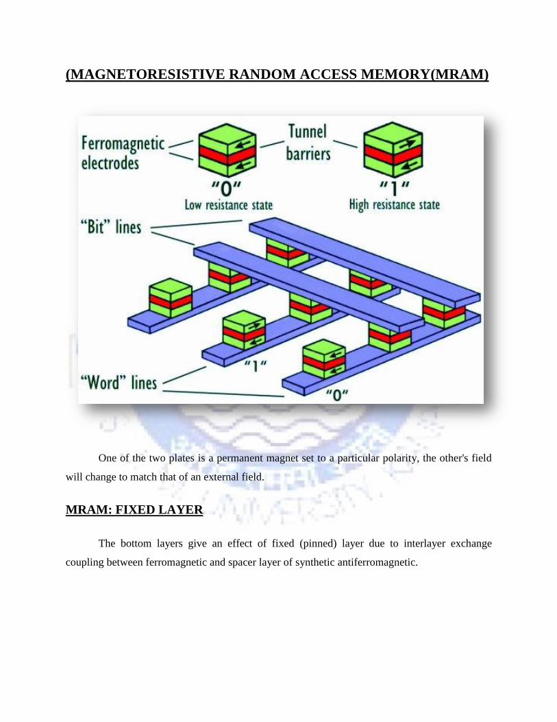
(MAGNETORESISTIVE RANDOM ACCESS MEMORY(MRAM)
One of the two plates is a permanent magnet set to a particular polarity, the other's field
will change to match that of an external field.
MRAM: FIXED LAYER
The bottom layers give an effect of fixed (pinned) layer due to interlayer exchange
coupling between ferromagnetic and spacer layer of synthetic antiferromagnetic.

MRAM: READING PROCESS
• Transistor is “ON”
• Measuring of electrical
resistance of a small sense
current from a supply line through
the cell to the ground.
MRAM: WRITING PROCESS
Transistor is “OFF”
When current is passed through
the write lines, an induced magnetic
field is created at the junction, which
alters the polarity of the free layer.

In order to change the polarity of the
free layer, both fields are necessary.
Only the bit in which current is applied
in both hard and easy axis will be written. The
other bits will remain half-select.
MRAM: CHARACTERISTICS
• Non-volatility
• Infinite endurance
• High speed performance
• Low cost
MRAM V/S OTHER RAM TECHNOLOGIES

FUTURE MRAM IMPROVEMENTS
Thermal Assisted Switching
• Solves the first-generation selectivity and
stability problems
• Cost-effective and scalable memory
technology to at least the 32nm node
MRAM STATUS
• 2003 - A 128 Kbit MRAM chip was introduced, manufactured with a 180 nm
lithographic process
• 2004 - Infineon unveiled a 16-Mbit prototype, manufactured with a 180 nm lithographic
process
• 2005 - Sony announced the first lab-produced spin-torque-transfer MRAM
• 2007 - Tohoku University and Hitachi developed a prototype 2 Mbit Non-Volatile RAM
Chip employing spin-transfer torque switching
• 2008 - Scientists in Germany have developed next-generation MRAM that is said to
operate with write cycles under 1 ns.
• 2009 - Hitachi and Tohoku University demonstrated a 32-Mbit spin-transfer torque RAM
(SPRAM)
ADVANTAGES OF SVT (SPIN VALVE TRANSISTOR)
Traditional transistors use on & off charge currents to create bits – the binary 0&1 of Computer
information. Quantum spin field effect transistor will use up & down spin states to generate the
same binary data.
A currently logic is usually carried out using conventional electrons, while spin is used for
memory. Spintronics will combine both.
In most Semi Conducting transistors the relative proportion of the up & down carries types are
equal. If Ferro Magnetic material is used as the carrier source then the ratio can be deliberately
skewed in one direction.
Amplification and / or switching properties of the Device can be controlled by the external
magnetic field applied to the device.
One of the problems of charge current electrons is that we pack more devices together, the chip
heats up. Spin current releases heat but it is rather less.
LIMITATIONS
Controlling spin for long distances.
Difficult to INJECT and MEASURE spin.
Interference of fields with nearest elements.
Control of spin in silicon is difficult.
APPLICATIONS:
Spin transistors have huge potential for incorporation in stable, high sensitivity magnetic
field sensors for automotive, robotic, mechanical engg. & data storage applications.
This may also be used as Magnetically Controlled Parametric Amplifiers & Mixers, as
magnetic signal processors, for control of brush less DC motors & as Magnetic Logic
elements.
In log applications they have the advantage over conventional semiconductor chips that they
do not require power to maintain their memory slate. It finds its application towards
Quantum Computer, a new trend in computing. Here we use Qubits instead of bits. Qubit
also represents only 1& 0 but here they show superposition these classical states. But it is in
pioneering stage.
There are major efforts ongoing at Honeywell, IBM, Motorola in developing RAM based on
spin valves and metal tunnel junctions such devices called MRAM have demonstrated faster
speed, high density low power consumption, non-volatility and radiation harness they are
promising replacements for the Semi Conducting RAM currently used.
CONCLUSION
Perhaps the most influential aspect of the SVT is that it showed the value of functional
integration of semiconductor and ferromagnetic materials into hybrid electronic devices. Room
temperature effects as large as 400% in small magnetic fields are now routinely obtained, a
feature that has attracted significant attention. Much progress has been made in optimizing
device performance, focusing on the output current level and noise sources. Further
improvements are still required in order to capitalize on the huge magnetic sensitivity of such
structures for application in magnetic field sensors or magnetic memories.
At the same time, the SVT opened up a new route to systematically study the fundamental
physics of spin dependent transport of hot electrons at energies of the order of 1 eV. New
insights into the origin of spin-dependent hot-electron scattering have been obtained, including
the dominance of volume effects over interfaces in the spin dependence of the transmission, the
effect of thermal spin waves, and the surprisingly important role of elastic scattering processes.
The latter feature points to the relevance of establishing the precise relation between scattering
and structural properties of the devices, an area that has still remained largely unexplored. It also
hints at an interesting route to the next generation of devices in which epitaxial growth
techniques will be used to obtain transistors with high structural quality.
The basic concept of the SVT has also led to the development of a number of related device
structures such as the MTT (Magnetic Tunnel Transistor). The tunability of the hot-electron
energy provides unique possibilities for spectroscopic studies, while enhanced base transmission
is anticipated. Moreover, it has been realized that hot-electron spin filtering may have some
attractive features for spin-injection into a semiconductor, in particular the ability to reach a spin
polarization near 100% with conventional ferromagnets. Work that is in progress will soon
provide more information on the feasibility of this approach.
Another interesting research avenue we are currently exploring is the study of hot-electron spin-
transport in novel materials such as half-metallic ferromagnets and oxides. Such materials may
also offer new types of hybrid electronic devices combining ferromagnets and semiconductors.