PM6507 Transistor Curve-tracer
102
HILIPS
-
Upload
khangminh22 -
Category
Documents
-
view
3 -
download
0
Transcript of PM6507 Transistor Curve-tracer

HILIPS

t~tC-, ~ ~ i~y I
..
A A
A
- PHILIPS
TRANSISTOR CURVE-TRACER PM 6507 9452 065 07. t
9499 520 04511 1/469/1/04
Manual
2
CONTENTS
GENERAL
I. INTRODUCTION 7
II. WORKING PRINCIPLE 7
^~ III. BLOCK DIAGRAM 8 1. Control section 8 2. Display section i2
IV. TECHNICAL DATA 13
V. ACCESSORIES 15
DIRECTIONS FOR USE
VI. INSTALLATION 17
A. Adjustment to the local mains voltage 17 B. Earthing 17 C. Connection to the mains 17 D. Rack mounting version 18
VII. OPERATING INSTRUCTIONS 19
A. Survey of the controls 19 B. Hints for testing semi-conductors 19 C. Functions of the controls 19 D. Operation 23
1. Basic setting 23 2. Switching-on the apparatus 23 3. Connection of asemi-conductor 23 4. Adjusting the display section 23 5. Setting for testing semi-conductors with 3 or 4 terminals 23 6. Setting for breakdown tests of diodes and other elements with 2 connections 26 7. Setting for external control or programming 27
SERVICE DATA
VIII. CIRCUIT DESCRIPTION 37
A. Supply section 37 ,_, 1. Mains supply 37
2. Collector voltage supply 37 3. H.T. supply 37 4. Direct voltage source +31.51 +300x'-30 V 37
B. Step generator 39 1. Phase shifter, amplifier and rectifier, pulse shaper 39 2. Duty cycle 39
,^, 3. Ring counter 39 4. Amplifier 43 5. Power amplifier 44
C. Display section 44 1. Circuit for I, • and V, l; measurements 45 2. Circuit for Vi;l.; measurements 46 3. Circuit for breakdown voltage and leakage current measurements 47
,_ 4. Difference amplifier for X and Y-deflection 48 5. Output amplifiers for X and Y-deflection 48
6. Brightness control 48
IX. DISASSEMBLY 49
A. Cabinet 49 B. C.R.T. 49

3
C. Removing the subunits D. Removing components
X. MAINTENANCE
XI. SURVEY OF ADJUSTING ELEMENTS
XII. CHECKING AND ADJUSTING
A. Direct voltages -x-30 V and —30 V B. EHT unit 4.5 kV C. 3 kV voltage for testing diodes D. Step generator E. Collector voltage supply F. Monitor
XIII. THE SHIPMENT OF THE INSTRUMENT
52 57
61
62
63
63 64 64 64 64 65
67
XIV. LISTS OF PARTS 68

4
LIST OF FIGURES
1 2 3 4 5
Basic construction Block diagram Accessories Rear side of the instrument Making the instrument suitable fora 19" rack
6 10 15 17 18
6 7 ~ Basic considerations for testing semi-conductors 19 8 9 Front view with controls and sockets 20
10 Trigger point 20 11 Effect of the duty-cycle control 24 12 Curve display with current limiting 24 13 Breakdown characteristics 25 14 Compensation for the rion-linear part of the base-emitter diode characteristic 25 15 I„-V„<-characteristic of an N-channel junction FET 26 16 I„-V„; -characteristic of a P-channel enhancement-type MOS-FET 26 i 7 Position of the screen over the semi-conductor under test 27 18 Display in positions n and C of PM 6546 27 19 Circuit for external programming 28
20 . 47 Various measurements with the curve tracer 29. . .35 48 Supply part 36 49 Collector-voltage source 36 50 H.T.-source 36 51 Step-voltage generator 38 52 Trigger circuit (U9) 38 53 Principle of the ring counter 40 54 Voltage-divider circuit 40
55a Switch position REP FAM 40 55b Switch position SINGLE FAM 41 55c Switch position ONE CURVE 42
56 Amplifier 43 57 Voltage drive 44 58 Collector-current circuit 45 59 Measuring circuit for V,;,; measurement 46 60 Measuring circuit for breakdown-voltage and leakage-current measurements 47 61 X-Power amplifier 49 62 Side view (left) 50 63 Top view 51 64 Bottom view 52 65 H.T. unit U2 (supply for C.R.T.), taken off 53 66 X-Deflection unit U3, taken off 53 67 Y-Deflection unit U4, taken off 54 68 Base-resistor unit U5, taken off 54 69 Shunt unit U6, taken off 55 70 Final-amplifier unit U8, taken off 55 71 Side view right 56 72 Step generator U9, taken off 57 73 Rear view (rear panel taken off) 58 74 Collector-load unit U10, taken off 58 75 H.T. unit U11 (3 kV), taken off 59 76 Socket unit U12, taken off 60 77 Push-button unit U15 and SK4, taken off 60 78 Adjusting the zener diodes 63 79 Adjusting the collector-voltage source 0-10 V 65 80 Hum influence on the C.R.T. 65 81 Adjusting the X-deflection 67 82 Adjusting the Y-deflection 67 83 Front view with item numbers 69 84 Rear view with item numbers 69 85 Side view (left) with item numbers 70 86 PM 6546 with item numbers 70

5
87 Diagram PM 6546 81 88 Printed wiring board PM 6546 81 89 Switch wafers SK2 82 90 Switch wafers SK10 82 91 Switch wafers SK12 82 92 Switch wafers SK13 82 93 Switch wafers SK16 83 94 Connection diagram for mains transformer T2 83 95 Connection diagram for collector transformers T3 and T4 83 96 Connection diagram for H.T. transformer T201 83 97 Connection diagram for H.T. transformer T1101 83 98 Printed wiring board U1, final amplifier 84 99 Printed wiring board U2, H.T. circuit 85
100 Printed wiring board U3A, pre-amplifier 86 101 Printed wiring board U3B, X-deflection 87 102 Printed wiring board U3C, X-deflection 88 103 Printed-wiring board U4A, pre-amplifier 89 104 Printed wiring board U4B, Y-deflection 90 105 Printed wiring board U4C, Y-deflection gt 106 Printed wiring board U5A, base resistors 92 107 Printed wiring board U6A, shunt plate 93 108 Printed wiring board U7, power supply 94 109 Printed wiring board U8A, final amplifier 95 110 Printed wiring board U9A, step generator 96 111 Printed wiring board U9B, ring counter g7 112 Printed wiring board U11A, high-tension unit 98 113 Printed wiring board U13, adjusting circuit 99 114 Circuit diagram of the intensity limiter 100 115 Circuit diagram 103
IMPORTANT
In correspondance concerning this apparatus, please quote the type number and serial number as given on the plate at the back of the apparatus.

6
POWER
SUPPLY
VAu'FI VOLTAGE
GENERATOR
STEP
GENERATOR
COLLECTOR
SUPPLY UNR
J
nA
COLLECTOR CURRENT
AMPLIFIER
Fig. 1 . Basic construction
VERTICAL -MODE~RANOES SELECTOR
TRANSISTOR UNDER TEST
HOR ZON7AL-MODENtANGES SELECTOR
AMPLIFIER
Y-DEFL.
CONTROL SECTION DISPLAY SECTION
AMPLIFIER
X-DEFL.

7
GENERAL
_ 1. Introduction
The PHILIPS Curve-tracer PM 6507 is a universal in-strument for measuring and determining the characte-ristics of transistors and diodes. On the square flat c.r.t. it is possible to display single curves as well as sets of curves (up to 8) in various modes. The swit-chable duty-cycle control circuit permits of displaying characteristics of power transistors up to their limits, without subjecting these transistors to thermal over-load.
_ The current and voltage sources for supplying the semi-conductors under test have a very wide range (I, max. 20 A, V,•~; max. 500 V).
11. Working principle
The simplified diagram of Fig. 1 shows the basic con-struction of the PM 6507. From this diagram it appears that the apparatus essentially consists of 2 sections, namely:
—the supply and control section, and —the display section with the c.r.t.
—The supply and control section comprise all control elements required for setting the desired mode of operation and adjusting the unit to the operating data of the semi-conductor under test. For testing a tran-
'~ sistor these are the collector and base supply vol-tages. For the collector circuit ahalf-wave voltage source of maximum 500 V is available. This voltage has been divided into four ranges, which can be selected by means of push-buttons, and is continu-ously adjustable within these ranges. The base circuit is driven by the step generator.
For testing the breakdown characteristics of diodes a separate H.T. source (max. 3000 V) is available.
Due to its special circuitry the curve tracer can satisfy the high standards set in semi-conductor measuring techniques.
It is therefore extremely suitable for being used in laboratories, but may also serve as a test apparatus for selecting and comparing semi-conductors with certain properties.
Dependent on the repetition frequency and the step value selected, a base signal is obtained which has the shape of a step curve. This will give rise to cur-rent and voltage variations in the collector circuit of the transistor under test which correspond to the properties of this transistor.
—The relevant data are applied to the display section and displayed on the c.r.t. It is possible to select a display method for the curve or set of curves which is in accordance with the operating mode of the transistor. The horizontal and vertical deflection amplifiers can be adjusted to optimum resolution over a wide range so that accurate and clear mea-surements can be made. For testing diodes in the breakdown region the apparatus has been provided with a separate HT generator which can supply voltages up to 3 kV.
8
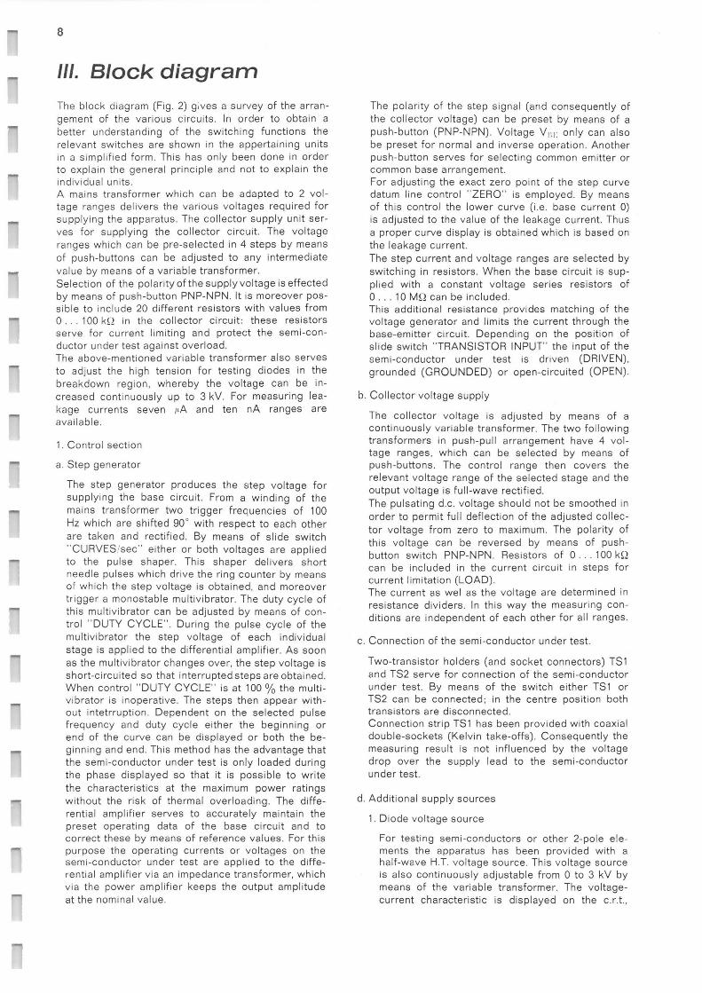
_ 111. Block diagram
The block diagram (Fig. 2) gives a survey of the arran-gement of the various circuits. In order to obtain a
~` better understanding of the switching functions the relevant switches are shown in the appertaining units in a simplified form. This has only been done in order to explain the general principle and not to explain the individual units. A mains transformer which can be adapted to 2 vol-tage ranges delivers the various voltages required for
_ supplying the apparatus. The collector supply unit ser-ves for supplying the collector circuit. The voltage ranges which can be pre-selected in 4 steps by means of push-buttons can be adjusted to any intermediate
_ value by means of a variable transformer. Selection of the polarity of the supply voltage is effected by means of push-button PNP-NPN. It is moreover pos-sible to include 20 different resistors with values from 0. . . 100 kS? in the collector circuit: these resistors serve for current limiting and protect the semicon-ductor under test against overload. The above-mentioned variable transformer also serves
—` to adjust the high tension for testing diodes in the breakdown region, whereby the voltage can be in-creased continuously up to 3 kV. For measuring lea-kage currents seven µA and ten nA ranges are available.
1. Control section
'— a. Step generator
The step generator produces the step voltage for supplying the base circuit. From a winding of the
_. mains transformer two trigger frequencies of 100 Hz which are shifted 90° with respect to each other are taken and rectified. By means of slide switch "CURVES sec" either or both voltages are applied to the pulse shaper. This shaper delivers short needle pulses which drive the ring counter by means of which the step voltage is obtained, and moreover trigger a monostable multivibrator. The duty cycle of
—" this multivibrator can be adjusted by means of con-trol "DUTY CYCLE". During the pulse cycle of the multivibrator the step voltage of each individual stage is applied to the differential amplifier. As soon as the multivibrator changes over, the step voltage is short-circuited so that interruptedsteps are obtained. When control "DUTY CYCLE" is at 100 %the multi-vibrator is inoperative. The steps then appear with-out intetrruption. Dependent on the selected pulse frequency and duty cycle either the beginning or end of the curve can be displayed or both the be-
_ ginning and end. This method has the advantage that the semi-conductor under test is only loaded during the phase displayed so that it is possible to write the characteristics at the maximum power ratings without the risk of thermal overloading. The diffe-rential amplifier serves to accurately maintain the preset operating data of the base circuit and to correct these by means of reference values. For this
—` purpose the operating currents or voltages on the semi-conductor under test are applied to the diffe-rential amplifier via an impedance transformer, which via the power amplifier keeps the output amplitude
~" at the nominal value.
The polarity of the step signal (and consequently of the collector voltage) can be preset by means of a push-button (PNP-NPN). Voltage V,;,; only can also be preset for normal and inverse operation. Another push-button serves for selecting common emitter or common base arrangement. For adjusting the exact zero point of the step curve datum line control "ZERO" is employed. By means of this control the lower curve (i.e. base current 0) is adjusted to the value of the leakage current. Thus a proper curve display is obtained which is based on the leakage current. The step current and voltage ranges are selected by switching in resistors. When the base circuit is sup-plied with a constant voltage series resistors of 0. . . 10 MS? can be included. This additional resistance provides matching of the voltage generator and limits the current through the base-emitter circuit. Depending on the position of slide switch "TRANSISTOR INPUT" the input of the semi-conductor under test is driven (DRIVEN), grounded (GROUNDED) or open-circuited (OPEN).
b. Collector voltage supply
The collector voltage is adjusted by means of a continuously variable transformer. The two following transformers in push-pull arrangement have 4 vol-tage ranges, which can be selected by means of push-buttons. The control range then covers the relevant voltage range of the selected stage and the output voltage is full-wave rectified. The pulsating d.c. voltage should not be smoothed in order to permit full deflection of the adjusted collec-tor voltage from zero to maximum. The polarity of this voltage can be reversed by means of push-button switch PNP-NPN. Resistors of 0. . . 100 k5? can be included in the current circuit in steps for current limitation (LOAD). The current as wel as the voltage are determined in resistance dividers. In this way the measuring con-ditions are independent of each other for all ranges.
c. Connection of the semi-conductor under test.
Two-transistor holders (and socket connectors) TS1 and TS2 serve for connection of the semi-conductor under test. By means of the switch either TS1 or TS2 can be connected; in the centre position both transistors are disconnected. Connection strip TS1 has been provided with coaxial double-sockets (Kelvin take-offs). Consequently the measuring result is not influenced by the voltage drop over the supply lead to the semi-conductor under test.
d. Additional supply sources
1. Diode voltage source
For testing semi-conductors or other 2-pole ele-ments the apparatus has been provided with a half-wave H.T. voltage source. This voltage source is also continuously adjustable from 0 to 3 kV by means of the variable transformer. The voltage-current characteristic is displayed on the c.r.t.,

n n
w w w w w w A A A
COLLECTOR SUPPLY PART
r
8
~b r
i a
0 0
3a ga
l.#.1 .l,T.J ♦ L J
(""t
STEP GENERATOR
-Q
a~qa I
DIS
PLA
Y
SE
CTI
ON
C
ON
TRO
L S
EC
TIO
N~—
~ "~ a ~¢ w c>~~ ~ a o w m
s r
~~u d
W Na
a~
~e
m a
—_~_ —__~+___--~—
E
Fig.
2. B
lock
dia
gram
12
whereby 3 voltage measuring ranges are available which can be reduced by a factor 10 with push-button x.1, as well as several switchable ranges
._ for uA and nA measurements. Push-button "Read" connects the H.T. circuit only when it is closed manually or by means of a pro-tection device.
2. Voltage source for fourth electrode Connection socket "S" on the transistor holder, apart from earthing the transistor case (e.g. with
._,,, H.F. transistors), may also serve for connecting e.g. a second gate in case of field effect transis-tors. For this a variable direct voltage of max. 10 V can be applied (Shield Voltage), whose polarity can be selected by means of a switch.
2. Display section
The display section of the curve tracer does not affect —. the working of the other sections. After having passed
the relevant circuits and after being amplified the vol-tage or current changes occuring in the transistor are displayed on the c.r.t. Two step-switches serve for range selection and mode selection for the horizontal and vertical deflection. The horizontal deflection comprises 12 collector vol-tage ranges, 4 base voltage measuring ranges, one step range position, 3 ranges for diode test voltages and position "EXT" for external control. By means of the step switch for the vertical deflection the collector current range is selected in 18 steps,
s
whereby the sensitivity of 10 steps can be increased
by a factor 103 for measuring diode leakage currents. Moreover, the base voltage measuring sensitivity can be adjusted in 4 steps by means of this switch and an additional position is available for external control. By means of a slide switch all vertical deflection ranges can be extended to either side by a factor 0.5 and 5. To enable proper curve display in case of an inverted signal, a switch has been provided by means of which the polarity of the horizontal and vertical deflection voltages can be reversed. This switch also serves for switching on the calibration voltage ("CAL"). The voltages present on the semi-conductor (or the current relations) are not influenced by the display section. Therefore the operating voltages for the semiconduc-tor under test are applied to the differential amplifiers via high-ohmic input stages. The output amplifiers supply the power required for the magnetic deflection, whereby the trace can be shifted in the horizontal and the vertical direction by means of the combined coarse and fine controls.
The acceleration voltage for the picture tube is delive-red by a 4.5 kV generator. In order to keep the brightness of the picture constant at different sweep speeds a brightness modulator has been provided which increases the intensity at the higher speeds. The brightness of the picture is also influenced by control "Duty Cycle".

13
IV. Technical data
—" Tolerances: Numerical values with statement of tole-rances are guaranteed by the factory. Data without tolerances serve merely for information and represent the properties of an average apparatus.
Step generator
_,,,, Step current generator:
,,,,,
Current steps (constant current values)
Number of curves
Stability of the step spacings
Stability of the current generator
Step voltage generator: Voltage steps mV/step max. internal resistance 2: (current per step 200 mA)
Switchable source resistors
Duty cycle
Zero adjustment of the step voltage
1, 2, 5µA etc . . .200 mA/step (17 steps plus a 0 -step) All current steps can be doubled for a brief period
7 (8 with datum line) adjustable from 2 . . . 8
Between the first and seventh step within an arbitrary range < 1 %; with respect to each other: in all ranges < 3
A load variation of 0.1 V at 1 V causes an error of < 1 % in all ranges
0 20 50 100 200 500 1000 0.1 0.1 0.25 .5 1 2.5 5 All voltage steps can be doubled for a brief period
steps: 0, 1, 2, 5 4 etc . . . 10 MQ (23 steps)
at 100 pulses/sec. 250 sus . . . 6 ms (2.5%. . .60%and 100% at 200 pulses/sec. the same pulse times apply, however, twice the duty cycle in percentages. Overlap from 4 ms.
Can be shifted 100 % (7 steps) in the positive or negative direction (at 200 mA/step and all mV/step ranges max. 12 V at 30 %duty cycle).
Collector supply
Rectified sine-wave voltage, continuously adjustable in 4 ranges Voltage range Max. current Internal resistance Ri
(at 220 V)
0 . . . 10 VP _ 20 A 0.3 2 0. . . 50Vp _~, 4 A 3.8 S2 0. . . 100VP _ u 2 A 16 S? 0. . .500 V~, _ u 0.2 A 400 52
Polarity
Overload protection
—• Current limitation
Connection sockets BU2B
Diode voltage source
Voltage range
Maximum load current
Short circuit current
..., Internal resistance
Voltage sourcefor 4th electrode
Reversible by means of button PNP-NPN
By means of thermo-magnetic switch. Response time at 2x the nominal current: approx. 15 secs. Response time at 10x nominal current: 0.05 secs. at max.
By means of switchable series resistors. Resistance scale: 0, 0.1, 0.2, 0.5 2 etc . . . 100 k~ ± 10 % (20 steps)
provided with Kelvin take-offs when adapter PM6549A is used.
(continuously adjustable half-wave voltage) 0. . .3000 V„ _ ~
1 mA
8 mA~, _„ at max.
370 kS?
0 . . . 10 V; continuously adjustable from 0 to + or —10 V Connection to the "S" socket
14
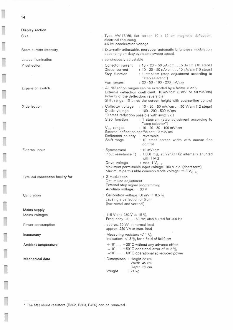
Display section
C.r.t. :Type AW 17/69, flat screen 10 x 12 cm magnetic deflection, electrical focussing.
~' 4.5 kV acceleration voltage
Beam current intensity Externally adjustable, moreover automatic brightness modulation depending on duty cycle and sweep speed.
"~ Lattice illumination : continuously adjustable
Y-deflection :Collector current 10 - 20 - 50 µA/cm . . . 5 A/cm (18 steps) Diode current 10 - 20 - 50 nA/cm . . . 10 ~~A/cm (10 steps)
—. Step function 1 step/cm (step adjustment according to "step selector")
V~;~; ranges 20 - 50 - 100 - 200 mV/cm
Expansion switch :All deflection ranges can be extended by a factor .5 or 5. _ External deflection coefficient: 10 mV/cm (5 mV or 50 mV/cm) Polarity of the deflection: reversible Shift range: 10 times the screen height with coarse-fine control
X-deflection :Collector voltage 10 - 20 - 50 mV/cm . . . 50 V/cm (12 steps) Diode voltage : 100 - 200 - 500 V/cm 10 times reduction possible with switch x.1 Step function 1 step/cm (step adjustment according to
"step selector") V,; ,; ranges 10 - 20 - 50 - 100 mV/cm External deflection coefficient: 10 mV/cm Deflection polarity : reversible Shift range 10 times screen width with coarse fine
control
External input : Symmetrical 10 mV/cm '- Input resistance *) : 1,000 mS?, at Y2/X1/X2 internally shunted
with 1 MS? Drive voltage max. 1 VP_n Maximum permissible input voltage: 100 V d.c. (short-term)
"" Maximum permissible common mode voltage: ~- 8 V„_ I,
External connection facility for Z-modulation Datum line adjustment
_. External step signal programming Auxiliary voltage: + 30 V
Calibration :Calibration voltage: 50 mV ± 0.5 causing a deflection of 5 cm
~" (horizontal and vertical)
Mains supply
Mains voltages 115 V and 230 V ± 15 Frequency: 40. . .60 Hz; also suited for 400 Hz
Power consumption approx. 50 VA at normal load approx. 250 VA at max. load
Inaccuracy Measuring resistors < 1 Indication: < 3 % for a field of 8x10 cm
Ambient temperature +10° . . . +35°C without any adverse effect ,_ —10° . . . -{-50`C additional error of ± 2
—20° . . . -I-60°C operational at reduced power
Mechanical data :Dimensions :Height 22 cm Width 45 cm Depth 32 cm
Weight 21 kg
* The MQ shunt resistors (R362, R363, R426) can be removed.

15
V. Accessories
-- t Mains cable 2 Transistor adapters PM 6549 (for L.F. and power transistors) 1 Manual Optional accessories: Transistor adapter PM 6544 for power transistors (case SOT9; DIN 9A2) Transistor adapter PM 6547 (for RF transistors) Transistor adapter PM 6548 (empty case for mounting special holders) Transistor adapter PM 6549A (for power transistors, with Kelvin take-offs) Diode adapter PM 6546 Polaroid camera assy PM 9380 Camera adapter PM 9377 Supplementary Cense PM 9373
PM 6547
Fig. 3. Accessories
PM 6548 PM 6549
PM 6544
PM 8549A
17
DIRECTIONS FOR USE
.~ Vl. Installation
A. ADJUSTMENT TO THE LOCAL MAINS VOLTAGE
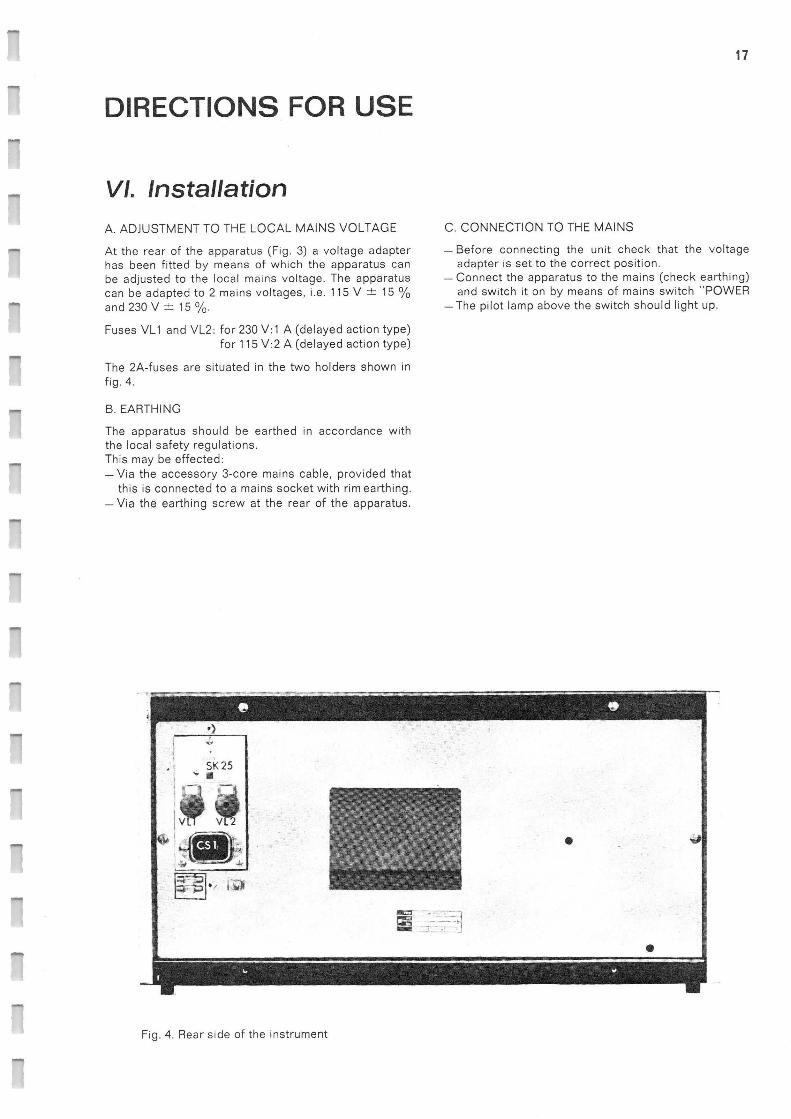
-- At the rear of the apparatus (Fig. 3) a voltage adapter has been fitted by means of which the apparatus can be adjusted to the local mains voltage. The apparatus can be adapted to 2 mains voltages, i.e. 115 V -~- 15
~' and230V -j - 15%.
Fuses VL1 and VL2: for 230 V:1 A (delayed action type) for 115 V:2 A (delayed action type)
The 2A-fuses are situated in the two holders shown in fig. 4.
— B. EARTHING
The apparatus should be earthed in accordance with the local safety regulations.
_ This may be effected: —Via the accessory 3-core mains cable, provided that
this is connected to a mains socket with rim earthing. —Via the earthing screw at the rear of the apparatus.
C. CONNECTION TO THE MAINS
— Before connecting the unit check that the voltage adapter is set to the correct position.
—Connect the apparatus to the mains (check earthing) and switch it on by means of mains switch "POWER
—The pilot lamp above the switch should light up.
Fig. 4. Rear side of the instrument
18
D. RACK-MOUNTING VERSION
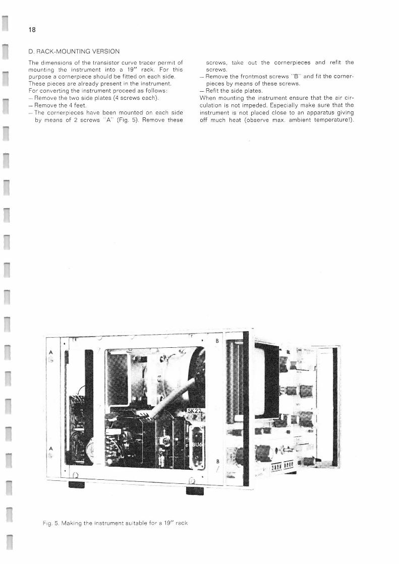
The dimensions of the transistor curve tracer permit of _.. mounting the instrument into a 19" rack. For this
purpose a cornerpiece should be fitted on each side. These pieces are already present in the instrument. For converting the instrument proceed as follows:
... —Remove the two side plates (4 screws each). —Remove the 4 feet. —The cornerpieces have been mounted on each side
by means of 2 screws "A" (Fig. 5). Remove these
i
A A A ..,
A A A t 1
Fig. 5. Making the instrument suitable fora 19" rack
screws, take out the cornerpieces and refit the screws.
—Remove the frontmost screws "B" and fit the corner-pieces by means of these screws.
— Refit the side plates. When mounting the instrument ensure that the air cir-culation is not impeded. Especially make sure that the instrument is not placed close to an apparatus giving off much heat (observe max. ambient temperature!).
19
V11. Operating instructions
A A A A A A R A A A A
A A
n A
ATTENTION:
The collector supply source permits adjustment of vol-tages up to 500 V,,,.;,i; with respect to earth. At the high tension output this is even as high as 3000 V,,,.;,,; with respect to earth. Voltages exceeding 34 V,,,.;,,; may be lethal. When inserting the semi-conductor under test into the sockets or adapter, switch SK18 should always be in position "OFF"! The semi-conductor connection is then interrupted at three points. The utmost of care should be taken when working with high supply voltages. For testing diodes with the aid of the high-tension source, it is advisable to use the special adapter PM 6546, described in this manual.
A. SURVEY OF THE CONTROLS see Fig. 9
B. HINTS FOR TESTING SEMI-CONDUCTORS
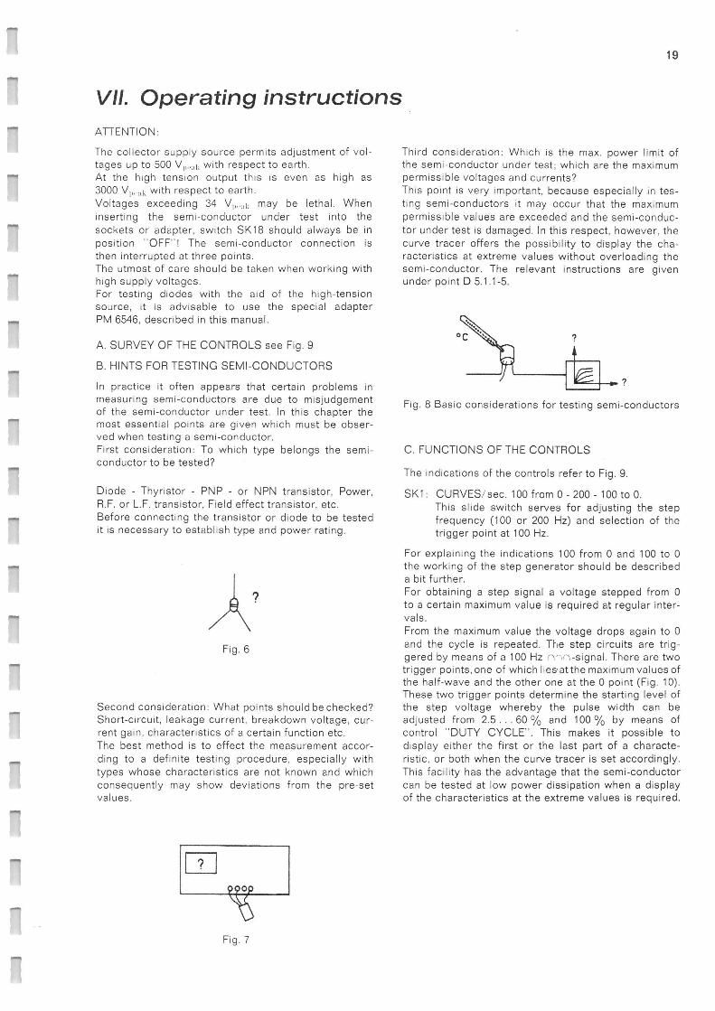
In practice it often appears that certain problems in measuring semi-conductors are due to misjudgement of the semi-conductor under test. In this chapter the most essential points are given which must be obser-ved when testing asemi-conductor. First consideration: To which type belongs the semi-conductor to be tested?
Diode - Thyristor - PNP - or NPN transistor, Power, R.F. or L.F. transistor, Field effect transistor, etc. Before connecting the transistor or diode to be tested it is necessary to establish type and power rating.
~' Fig. 6
Second consideration: What points should be checked? Short-circuit, leakage current, breakdown voltage, cur-rent gain, characteristics of a certain function etc. The best method is to effect the measurement accor-ding to a definite testing procedure, especially with types whose characteristics are not known and which consequently may show deviations from the pre-set values.
Fig. 7
Third consideration: Which is the max. power limit of the semi-conductor under test; which are the maximum permissible voltages and currents? This point is very important, because especially in tes-ting semi-conductors it may occur that the maximum permissible values are exceeded and the semiconduc-tor under test is damaged. In this respect, however, the curve tracer offers the possibility to display the cha-racteristics at extreme values without overloading the semi-conductor. The relevant instructions are given under point D 5.1.1-5.
Fig. 8 Basic considerations for testing semi-conductors
C. FUNCTIONS OF THE CONTROLS
The indications of the controls refer to Fig. 9.
SK1: CURVES/sec. 100 from 0 - 200 - 100 to 0. This slide switch serves for adjusting the step frequency (100 or 200 Hz) and selection of the trigger point at 100 Hz.
For explaining the indications 100 from 0 and 100 to 0 the working of the step generator should be described a bit further. For obtaining a step signal a voltage stepped from 0 to a certain maximum value is required at regular inter-vals. From the maximum value the voltage drops again to 0 and the cycle is repeated. Tf~e step circuits are trig-gered by means of a 100 Hz nnn-signal. There are two trigger points, one of which lies~atthe maximum values of the half-wave and the other one at the 0 point (Fig. 10). These two trigger points determine the starting level of the step voltage whereby the pulse width can be adjusted from 2.5. . .60 % and 100 % by means of control "DUTY CYCLE". This makes it possible to display either the first or the last part of a characte-ristic, or both when the curve tracer is set accordingly. This facility has the advantage that the semi-conductor can be tested at low power dissipation when a display of the characteristics at the extreme values is required.

20
R 301 1 R 302 E
f ~ ~~ ~ ~i1 SB 13L~~ -,~S~K` SK 10. SK 15 ~1. ~_
~✓ R 303 ~ ~ ~~
. C~ - .~o..,,, off,e<n~ A 403
Fig. 9. Front view with controls and sockets
0
L
0
SK 6 SN 7
~~ ~e~
l
0
SK t
~ee ~ ~t ~:
SK 3
SK RIR9
si !s, ~ ~, ~ ` ~BU 3a BlM2a ~ ~S , s
c
DN t1~D5
COt1fC!~R
Pulse witdh adjustable with
"DUTY CYCLE" control
1g0 cycles from 0
i
I
~ ~ 00 cvcles to 0 --~— --~ .. I
I
___. ~ _ _ ~ 2Uil cvcles
PEM 3841
Fig. 10. Trigger point

21
SK2 SOURCE RESISTANCE <2 It is possible to include a number of resistors from 0. . . 10 MS2 in series with base circuit.
-'~ These resistors serve for current limitation as well as for matching the base circuit.
SK3 This step switch serves for selection of the —, number of steps (or curves) to be displayed.
SK4 RANGE10V-50V-100V-500V Push-button switch for selection of the col-
,~ lector voltage range.
SK5 CUT OUT Excess-current cut-out for the collector vol-tage supply. This thermo-magnetic switch cuts out at an excessive primary current. Resetting is effected by depressing the red button.
SK6 READ This push-button serves for starting anon-recurrent curve display or, in case of single curve display, for switching to the next step of the characteristic.
SK7 ONE CURVE -SINGLE FAM. -REP. FAM —' Slide switch for trigger-mode selection
ONE-CURVE -Single curve In this switch position only one curve is dis-played whereby switching to the next step is
'~ effected by means of push-button "READ", dependent on the number of curves selected by means of SK3. SINGLE FAM -One set of curves In case of triggering by means of push-button "READ" non-recurrent display of the selected set of curves is obtained.
_ This display method is employed for heavily loaded transistors which do not permit of long-term operation or for photographic re-cording.
_ REP. FAM. -Repeated display of the set of curves In this switch position the selected curves are permanently displayed.
SK8 R901 DUTY CYCLE
This control serves for adjusting the duration of a curve, i.e. for adjusting the pulse width of _.. the step signal (also see SK1). The potentiometer permits adjustment of the pulse width between 2.5. . .60 % and in the fully clockwise switch position a duty cycle of 100 % is obtained.
SK9 HIGH VOLTAGE Slide switch of switching on the H.T. genera-for for testing diodes as regards breakdown voltage. The switch also serves for selection of two measuring ranges, uA and nA. These ranges correspond to the ranges of range selector SK16.
SK10 STEP SELECTOR Range selector for adjusting the step values
""' of the base-emitter circuit. The switch covers the three groups of ranges «A, mA and mV/ step. The voltage or current step between two
successive curves is determined by this switch. However, the selected value should be taken into account when establishing the value of the signal on the c.r.t., when SK13 or SK16 is in position
SK10A x2. All current and voltage ranges can be doubled by means of this push-button (only for brief periods!).
SK11 TRANSISTOR INPUT Slide switch for switching the input potential: GROUNDED In this position the input of the semiconduc-tor under test is connected to earth. DRIVEN In this position the input of the semiconduc-tor under test is driven by the step generator. OPEN In this position the input of the semiconduc-tor under test is open-circuited.
SK12 COLLECTOR LOAD Step switch by means of which resistors of 0. . . 100 kS2 can be included in series with the collector circuit for current limiting and matching. In this way the power dissipation of transis-tors operated near their load limits can be adapted individually which proves to be very useful in practice.
SK13 COLLECTOR VOLTAGE -BASE VOLTAGE Range selector for horizontal deflection of the trace. The values indicated apply to 1 cm screen distance, independent of the step value selected with SK10, except for position ~! '
In latter position the step value of SK10 applies to 1 cm screen distance. Position "EXT." serves for external horizontal deflection. Connection is effected via BU6 (sensitivity 10 mV/cm).
SK13A x.1. With this push-button the ranges 100 V, 200 V and 500 V of SK13 can be reduced by a factor
SK14 SK15
10.
NORMAL - INVERSE -CALIBRATION
These slide switches serve for polarity rever-sal of the horizontal (SK14) or vertical deflec-tion (SK15). This enables reversal of the trace in both directions, independent of each other. Switch position "CAL" serves for checking the display circuit; a direct voltage of 50 mV is then applied to the amplifier inputs. The indications near range selectors SK13 and SK16 remain valid (with the exception of switch position ~ as well as the base vol-tage ranges 10. . . 100 mV/cm and 20. . .200 mV/cm). The trace on the screen will be 5 cm. For the ranges in brackets the range values selected should be observed, and in position srr! the
sensitivity is 100 mV/cm i.e. a shift of 0.5 cm.

22
SK16 COLLECTOR CURRENT -BASE VOLTAGE Range selector for vertical deflection of the trace. The range values apply to 1 cm screen dis-tance, independent of the step value chosen
with SK10, except for switch position __ ~ In this position the step value of SK10 holds
'~ good for 1 cm screen distance. Position "EXT" serves for external vertical deflection. Connection is effected via BU6 (sensitivity 10 mV/cm).
SK17 x.5 x 1 x 5 Expansion switch. By means of this switch the vertical deflection range (SK16) can be extended by a factor 2 in downward direction and by a factor 5 in the upward direction.
SK18 Toggle switch TS1 -OFF -TS2 for connecting —' semi-conductor TS1 or TS2. The connection
sockets for 4 mm plugs together with the transistor receptacles above these sockets are parallel connected via RF coils. When the toggle switch is in the left-hand position the left hand receptacles and sockets are connected (TS1) and in the right-hand
,_, position TS2 is connected. In the centre posi-tion the sockets and receptacles are discon-nected.
SK19 Push-button switch for PNP-NPN selection, changing over the Vi;~.; from normal to inverse (polarity reversal of the B-E junction) and changing over from common-emitter to com-
,,,,~ mon-base arrangement.
SK20 Slide switch for selecting the + or —10 V direct voltage (~--) which may be added to the "S" connection (shield). This voltage is for instance required for transistors with two inputs.
SK21 POWER ON ~` Mains switch for switching on the apparatus.
SK22 Slide switch for the use of the step-generator with external programming. _ (Accessible via an apperture in the left-hand cabinet plate.)
SK25 Mains voltage adapter 115 V/230 V -~- 15 —' (at the rear of the apparatus).
T1 VOLTAGE Variable transformer for adjusting the collec- for voltage and the high tension (when SK9 is switched on).
R1 Potentiometer for adjusting the "SHIELD" —. voltage from 0 to + or —10 (dependent on
the position of SK20).
R301 INTENSITY _. Potentiometer for brightness control.
R302
R 303
R401
R402
R403
8902
X-SHIFT Ganged potentiometer (coarse and fine adjustment) for horizontal shift of the trace.
Potentiometer for adjusting the d.c. balance of the X amplifier.
Y-SHIFT Ganged potentiometer (coarse and fine ad-justment) for vertical shift of the trace.
SCALE ILLUMINATION Potentiometer for adjusting the lattice illumi-nation.
Potentiometer for adjusting the d.c. balance of the Y amplifier.
ZERO Control for zero shift of the step signal. The lower curve is adjusted to datum or leakage current level by means of R902. For this adjustment SK11 is set at "OPEN", the datum line is read and after SK11 has been reset to "DRIVEN" the lower curve is adjus-ted to the reading obtained, by means of R902. The datum line is correctly adjusted if the curve does not shift when SK11 is switched from "DRIVEN" to "OPEN".
BU1 Earthing socket.
BU2a Transistor receptable for small types
BU2b Connection sockets for power transistors } Switch position TS1 Parallel connections
The E-B and C-S connections have been pro-vided with Kelvin take-offs (voltage and current fed-out separately to prevent measu-ring errors)
BU3a Transistor receptacle for small types
BU3b
BU4 BU5
BU6
D1
LA1
LA2 LA3
Connection sockets for power transistors Switch position TS2 Parallel connections
BNC sockets for connection of a protective holder or connection cable for testing diodes in the breakdown region (max. 3 kV). (BU4 =measuring input) (BU5 =high voltage output ~ )
Multiple connector for external control (on the left hand side of the apparatus)
Push-button to connect the high voltage to socket BU5.
On/off pilot lamp
Lamps for lattice illumination
CS1 Mains socket with rim-earthing contacts (at the rear of the apparatus).

23
D. OPERATION
1. Basic setting
The basic setting of the apparatus depends on the type of semi-conductor and its characteristics as well as on the selected mode.
"' E.g., for measuring an NPN transistor of relatively low power the setting shown in Fig. 20 may be used. It is advisable to start with a low setting in case of a semi-conductor whose characteristic values are not exactly known. This setting can then be changed if amore accurate measurement is permissible.
2. Switching on the apparatus.
After the controls have been set to the initial position, the apparatus can be switched on with switch "POWER ON". If the transistor is already connected it should be
—" ensured that toggle switch SK18 is in the mid position; in this position the semi-conductors (TS1 and TS2) under test are disconnected. The heating up time of the curve tracer is approxima-tely 1 minute. After this the apparatus is ready for operation.
3. Connecting of asemi-conductor
For connection of small transistors two receptacles are available and two socket connectors for 4 mm plugs.
"~ The socket connector and the receptacles above it are parallel connected via R.F. chokes. These chokes pre-vent or suppress parasitic oscillation of R.F. transis-tors which for the same reason should be connected to the plug connectors. In the left-hand position of the toggle switch the left-hand receptacles and sockets (TS1) are connected and
„~ in the right-hand position the right-hand sockets and receptacles (TS2).
4. Adjusting the display section
The display section should be adjusted to the correct horizontal and vertical sensitivity before the semi-conductor under test is connected. First adjust the spot on the screen by means of the X and Y shift controls. The horizontal deflection corresponds to the collector-emitter voltage. As soon as a voltage is applied a horizontal line is displayed on the screen whose length
_ is a measure of the sensitivity adjusted with SK13 or the collector voltage. The vertical deflection defines the value of the collec-tor current of the transistor. Before the semi-conductor
_, is connected range selector SK16 should be set to a sensitivity corresponding to the collector current to be expected. As soon as a transistor is connected a current will flow through the collector circuit which depends on the selected base current or voltage. This current causes a deflection in the vertical direction on the screen, whereby the distance from the datum line to any point
'^ of the curve represents the value of the collector current. The switches NORM./INVERT serve for reversing the trace in the horizontal and vertical direction. An expan-
-"' sion switch permits of extending the vertical measuring range by a factor 2 in the upward direction or by a factor 5 in downward direction.
For the voltage ranges 100 V, 200 V and 500 V of the high voltage generator, apush-button has been provi-ded, which enables an increase of the display sensiti-vity by a factor 10. Control INTENSITY serves for adjusting the intensity of the electron beam. To prevent damaging of the picture tube the beam current intensity should not be excessive, but should be adjusted so that a clear picture is obtained. Balance-adjustment of the horizontal deflection is effected with potentiometer R303. If a VI;i.; of 20 mV, 50 mV or 100 mV is selected with SK13, R303 should be adjusted so that the movement of the spot is minimum (SK11 at "GROUNDED"). Balance-adjustment for the vertical deflection is effec-ted with 8403. While setting SK17 from 1 to x0.5 or x5, R403 should be adjusted so that the electron-beam shift is minimum.
5. Setting for testing semi-conductors with 3 or 4 terminals.
The following description gives a survey of the most important adjustments for displaying a characteristic. The example chosen applies to the display of I, as a function of Vc r;, with I1; as parameter, for a PNP tran-sistor in a TO 5 case.
— Set all the controls to the position shown in Fig. 20 (toggle switch TS1 -OFF -TS2 in the centre posi-tion).
— Switch on the apparatus (switch POWER ON).
—Insert the transistor in the receptacle, e.g. BU2a.
— Check and preset: — VcF. -VOLTAGE —COLLECTOR LOAD — STEP SELECTOR µA, mA/STEP — HORINZONTAL DEFLECTION (range) —VERTICAL DEFLECTION (range)
— Set the toggle switch at TS1.
—Adjust for desired step current (or step voltage and series resistance SK2 for certain traces), and collec-torvoltage.
—Adjust the horizontal and vertical deflection until proper curve display obtained.
—Adjust step switch "LOAD n" so that the curve dis-play is limited (e.g., according to the dotted line in Fig. 12).
—Adjust the level of the lower curve to zero with con-trol "ZERO" by setting slide switch SK11 at "OPEN" and reading the zero line (given by the leakage cur-rent of the transistor). Reset the slide switch at "DRIVEN" and adjust the lower curve to the zero value found by means of control "ZERO".
— By means of control "DUTY CYCLE" the driving time of the step current can be reduced, so that only the beginning of the curve is visible when switch "CURVES/sec." is at position "100 from 0", (Fig. 11 a). In position "100 to 0" the second part of the curve trace is visible (Fig. 11 b) and in position 200 the be-ginning and end of curve can be displayed, (see Fig. 11 c and description under point 5.1.2}.
24
i
5.1. Displaying curves with power limiting
The characteristics of semi-conductors at high loads can only be displayed when the semi-conductor cannot
"` be damaged by this high load. For this purpose the curve tracer offers the following possibilities:
5.1.1. Curve display with limited duty cycle of the step ~-- current (DUTY CYCLE) 100 from 0 or 100 to 0.
When a curve trace of a transistor is displayed the highest power dissipation occurs during the transition from the conductive to the non-conductive state. Fig. 12 shows a curve trace whereby the power dissipation limit P, max. of . . . mW is represented by the dotted line. This display method with limiting at P~;
,.~ max. can be approximated with the curve tracer. This is obtained by reducing the duty cycle of the step current (DUTY CYCLE) and by current limitation with series resistors included by means of the step switch (LOAD n). By means of the DUTY CYCLE control adjustment of the step width between 2.5. . .60 %and 100 % is possible (see Fig. 10 and the description under point C1).
_..
,.-.
(a)
(b) J..
Fig. 11. Effect of the duty-cycle control
(c)
These two methods enable reducing of the load of the semi-conductor under test to a minimum by displaying
—. only that part of the characteristic which is of interest. The semi-conductor may then be loaded to high values without the risk of being overloaded.
~. 5.1.2. Curve display with limited duty cycle of the step current, 200 Hz.
When the number of steps is even the curves are shifted to the beginning or end. In cases of an odd number all curves are uninterrupted but, dependent on the duty cycle adjustment, the centre parts are driven to zero and become consequently interrupted or over-
^ lap.
s
Fig. 12. Curve display with current limiting
In this way a survey of the entire characteristic is ob-tained at a limited load.
5.1.3. Curve display with current limiting by means of series resistors in the collector circuit.
Dependent on the base drive of a transistor currents will flow through the collector circuit which area fac-tor ht,, higher. When series resistors are included in the collector circuit a voltage drop will arise across this resistance which causes a decrease of the collec-tor-emitter voltage of the semi-conductor under test which depends on the transistor drive. In this way a power limitation is obtained which can be adapted to the maximum permissible value of the transistor and which can be adjusted to any value within the resis-tance and voltage ranges (Fig. 12).
5.1.4. Non-recurrent curve display
If certain transistor settings do not permit of conti-nuous operation, display in the "single" mode is possible. For this slide switch SK7 is set at "SINGLE FAM". Triggering is effected by means of push-button "READ" (SK6).
5.1.5. Curve display of one curve out of the set of curves.
From a set of curves, the number of which can be selected by means of switch STEP/FAM, each curve can be displayed individually. Switching over to a higher step is effected by means of push-button "READ" (SK6).
5.2. Displaying curves with voltage drive.
5.2.1. Transistors
a. Leakage current measurements I,~Et, I, Er,, !,_~;R -, I, r;;and breakdown voltage BV. (Fig. 13). Leakage current measurements I, i.;~t, as well as breakdown voltage measurements BV, •c~{ can be effected by means of the resistors from 0 S? (CES) to 10 M52 (CER) which can be switched by means of SK2 (SK10 in position 0 mV/Step). Open base mea-surements (Rf;F = x /CEO) can be effected with SK11 (INPUT OPEN). Measurements with voltage and resistance (CEX) can be effected as described above, however, SK10 should be adjusted to voltage (. . . mV/Step) and the polarity (SK19 A V,;,, INNERS) should be reversed. By means of control R902 "ZERO" any voltage value can be selected. During this measurement it should be observed that the power dissipation near the breakdown limits can be very high, so that it is recommended to limit the power dissipation by including resistors in the collector circuit.
b. Setting at small base currents:
Transistors with a high current gain can be measured most efficiently at a small I; • when the voltage drive on the base takes place via a high load resistance.

25
Example: 100 mV/step — 1 MS2
100 nA/ step.
}i A 10 510~
—~Imeas 1000
—►Imeos 100
i ~; _ 100 mV Compensation of the voltage in the non-linear part
— of the base-emitter diode characteristic is then possible by means of control R902 (Zero); see Fig.. 14.
1 M 52
Second Breakdown
10 'c;tK i ~ I ~ I 1 ICEB ~ ICEX , I ~ I
1- — — — -~' ~ I I ~ICBO I i I t t
BVCEO B CERBVCEB
Fig. 13. Breakdown characteristics
Ig
~--~ ► BVCEX IBVC80
VCEV
PEM 3840
nIg ~✓ i ~
---r o~
~ C BE
1
DC —SHIFT
PEM3B39
Fig. 14. Compensation for the non-linear part of the base-emitter diode characteristic
26
5.2.2. Voltage driven elements such as FET:
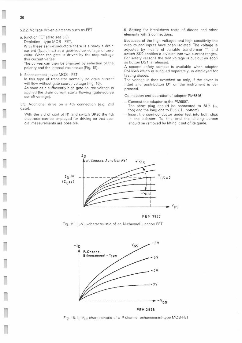
a. Junction FET (also see 5.3). Depletion -type MOS -FET. With these semi-conductors there is already a drain current (li ,, ,~, I„<:) at agate-source voltage of zero volts. When the gate is driven by the step voltage
,_ this current varies. The curves can then be changed by selection of the polarity and the internal resistance (Fig. 15).
b. Enhancement -type MOS -FET. In this type of transistor normally no drain current will flow without gate source voltage (Fig. 16). As soon as a sufficiently high gate-source voltage is applied the drain current starts flowing (gate-source cut-off voltage).
5.3. Additional drive on a 4th connection (e.g. 2nd _ gate).
With the aid of control R1 and switch SK20 tfie 4th electrode can be employed for driving so that spe-cial measurements are possible.
..,
Ip
N_Channel Junction Fet
6. Setting for breakdown tests of diodes and other elements with 2 connections.
Becauses of the high voltages and high sensitivity the outputs and inputs have been isolated. The voltage is adjusted by means of variable transformer T1 and switch SK9 enables a division into two current ranges. For safety reasons the test voltage is cut out as soon as button DS1 is released. A second safety contact is available when adapter PM 6546 which is supplied separately, is employed for testing diodes. The voltage is then switched on only, if the cover is fitted and push-button D1 on the instrument is de-pressed.
Connection and operation of adapter PM6546
- Connect the adapter to the PM6507. The short plug should be connected to BU4 (-, top) and the long one to BU5 (-F, bottom).
-Insert the semi-conductor under test into both clips in the adapter. To this end the sliding screen should be removed by lifting it out of its guide.
j D on
(I Dss)
+ VGS
V GS.0
PEM 3837
Fig. 15. I„-Vi,: -characteristic of an N-channel junction FET
-ID
P_Channel Enhancement -Type
VGS -6V
-5V
-4V
-3V
PEM 3838
-VDS
VDS
Fig. 16. I„-Vi,: -characteristic of a P-channel enhancement-type MOS-FET

27
For measurements in reverse direction, the cathode of the semi-conductor under test should be connec-ted to the positive clip (marked + ~^. ). This elec-
'r trode is connected to the high-voltage when the switch in the adapter is depressed.
— The screen has two different openings. Depending on the semi-conductor under test, the big or small opening can be chosen, so that the anode connec-tion is well screened against stray capacitance. Therefor the screen should be slided as far as pos-
,~, sible over the semi-conductor under test (Fig. 17). For insensitive measurements it is not necessary to use the screen.
5 I
Fig. 17. Position of the screen over the semi-conductor under test
r ~
Switching in
—Close the lid. Thereby the push-button SK1 is de-pressed automatically, by which the high-voltage connection of the semi-conductor under test is in-cluded into the circuit.
— Depress push-button DS1 on the PM6507; by this —' the high-voltage is switched in and applied to the
adapter.
WARNING
MEASUREMENTS WITH HIGH VOLTAGES HAVE TO BE CARRIED OUT WITH CLOSED LID ONLY. NEVER DEPRESS THE PUSH-BUTTON ON THE ADAPTER
—' MANUALLY.
Function of switch SK2
—' In position n_ normal operation with half-wave vol-tage occurs (Fig. 18, upper display). In position C a capacitor is incorporated into the high-voltage circuit. Consequently an integrated supply develops, so that the diode characteristic is not writ-ten from the origin. By this the influence of the switch and junction capacitance on the display is reduced. Nevertheless the breakdown of a diode can be obser-ved under dynamic conditions as a result of the super-imposed ripple voltage. By depressing push-button DS1 on the PM6507 perio-
_, dically, the complete quasi-static leakage-current or breakdown characteristics of the semi-conductor under test can be displayed. The fly-back occurs with atime-constant of 0.6 s. (Fig. 18, lower display).
REMARK
When switch SK2 occupies position C, a voltage drop ~"' arises over the capacitor load and the internal resis-
tance of the voltage source, so that only 70 % of the peak value of the half-wave voltage is available.
Fig. 18. Display in positions n and C of PM 6546
7. Setting the instrument for external control or pro-gramming:
a. Application as X-Y oscilloscope Connector BU6 on the left-hand side of the instru-ment can be employed for X-Y display. The inputs are arranged as follows: - Socket H/K
X1 Socket D X2 Socket F Y1 Socket B Y2 Socket E
b. Special measurements:
—Circuit for testing tunnel diodes —Circuit for simultaneous display of two charac-
teristics.
c. External programming of the step generator and external measuring circuits:
Automatic operation can be obtained by means of an external adapter. Independent of its normal appli-cation and the application as an X-Y oscilloscope the instrument can also be used as an automatic curve tracer. The external programming unit is connected to con-nector BU6 on the left-hand of the instrument. The basic arrangement for external programming appears from circuit diagram Fig. 19. The auxiliary unit should be proportioned so that it agrees with the application and type of semicon-ductor under test. The following formulas serve for calculating the desired operating values in the step voltage gene-rator and the collector supply. Selecting reference resistor Rx in the step gene-rator. This resistor determines the step current per stage.
100 For I ? 500 «A/step RL — I (mA/step) —1 ~n~
For I = 500 µA/step R~ _ 100
Collector voltage: This voltage should be preselected so that it corres-ponds to the max. test voltage. Lower voltages can be obtained by means of an external voltage devider (R, ), the series resistors simultaneously ensuring current limitation.

28
The horizontal deflection sensitivity of the monitor is determined by the two measuring voltage dividers A and B. These dividers can be made identical to the
^ internal divider (R346-R357 and R332-8334), whereby the intermediate stages which are not required may be left out.
Collector current:
Measuring resistance R ) is defined as follows:
.~ 10 mV/cm R) (~) — 1 mA/cm — 10 S2 Ri max ~ 10 k52
(1 mA has been chosen as an example)
_.
i
i
....
.~
SK22
BU6
o N
~ 0 1 0
R 36 5
M
UB
RX
I O
O
VBE
E o (BU 2b)
Base voltage:
For curve display as a function of the base-emitter voltage the X input should be connected to the base-emitter junction of the semi-conductor under test. The voltage divider to be employed should then be high-ohmic, so that the shunt of the base-emitter junction is small.
B O
Y r~
~ SO
F O _~_ I D
VC E
O
—r —
X ~ U ZERO STEP
p A t ~+30V I R V ,l
10 Kfl
RC
O
Z -MODULATION (Brightness control)
Fig. 19. Circuit for external programming
~ -30V PEM 3BG9
(BU 2 b)

29
A A
~n (c~ r~ ~c
~~~ e e ~ a 0
V I I I 0
~ A
0 0
0 0 o I ~~~~~~ l o
I~~~~I (o 0 0 0l m ~ o-
Fig. 20
Cc`i (bl Cc~ Cc~i ,~~01BB ,~p)8
® o
1 -'J
0
O
~ PI
0 ~0000l
I C%/////rJ I 0 m ~ o-
Fig. 21
6=
m
~_:~ ~ R.~~•~,
o ®/
o!~(/'1\
tt ~~JJ//1//:...
o~
m O;
O
o0 (c~ rdl tc'~ ~
o p o ® ~.
0 ® n O ool l0000j
Fig. 22
#~~
~_ __~ r T.
i ~ ~ <"J
~~ 0
a 0
~b o oogl 000J
I ~~~~~~ I ®n o
0
Fig. 23
Basic setting Adjust spot ® NPN-TRANSISTOR
Charact. IC = f (VCE) IB =Parameter
® NPN-TRANSISTOR
Common emitter p
Charact. IC = f (VCE) VBg =Parameter
® NPN-TRANSISTOR
Common emitter
Charact. IC = f (IB)
® NPN-TRANSISTOR
Common emitter
r-i~
~ =c

w 30
A w
A A A
G A
/( m
.ef Q~ ~C ~ I I I o
`tc
;~I
0E
~ ~ '~
°~Q~ ~
E~
O
A O
oO n :O) ,O i1
o ~•• -ogod 0000l ® n o-
Fig. 24
~s, ~ ~ ~ °~0~99'08
°~oj C~
; ,4 -o O ~J0000l l0000l
~ 1 G
Fig. 25
m ~ ~ ~
® o
~ -/ ~ ~~~ o 0 (c~ ~c Cc~ (c~
o~p~gg~p~g o
~,•o O ~ o
:L•zZ] l0 0 0 0l m ~ c3-
Fig. 26
~m :~
~~ ~
-- ~~
(( )) ~Ci1 ~ I I O
o ~
~
m
Vim
oo (~1 A B X01 B
o
b O I r. ' - o ,Qe SQ] l0000l m ~ o-
Fig. 27 V• \~
.=::s
Charact. Il; = f (VBE) Vi ~L =Parameter
I NPN-TRANSISTOR
Common emitter F.,, r ~:'>-
~ x=~B 1
~~ — -~ ~ I
Charact. VIE = f (VcE) IA =Parameter
t~ NPN-TRANSISTOR
Common emitter
1
Charact. I~ = f (VCB) Ig =constant
t~ ~~ NPN-TRANSISTOR
Common base~B
Charact. IC = f (IE) f,, ,~ NPN-TRANSITOR
®~ Common base
Y •I~
w

31
~C CC~ (c5l (C51
°~Q~A9~o 8 0
0
O) A
U O0
O
Q -o O I r L5: o
l0000l 0000l m n o-
Fig. 28
~~9
c a
o -o O f0000l
s~ ~ ~ 0
~ A o
0 0
l0000l ® ~ b
Fig. 29
Cc~i Cc~i ~ (~
o~pp~ B e
0
~ i ~ n
0
0 0
Q .-0 O
~b000l l0000l
i o
® COQ O
~~ i~; .-
>-Fig. 30
~ r~ ~ r~ °:~O~BB~p~@
m O
0 0
Fig. 31
~ r art' o
~~~~~
'"C:TT "
l0000l
I I Ei~;?a o
m ~ Q
e •z;acv
G'!%~ Yr
Charact. I;; = f (V~.;;) NPN-TRANSISTOR Common base
-i I- v:v, a
Charact. V~;B = f (V~B) IF =constant
NPN-TRANSISTOR Common base
IE
~~
R ai / ~~
-~:a
Charact. In = f (VDs)
Vcs =constant N CHANNEL FET
R V~
_ [] +VGs (NORMAL) ® —VGs (INNERS)
I I
Charact. I v = f (VDS) VGig =constant V~2s =Parameter
N CHANNEL FET with 2 gates
GPTE eoov SUBSTRATE
SCU RCE
1 1

32
~~ O (c~
01 990 8 ~.
m r ~c;l ~-+►I o
+~ O
0 O
C~ o O 0000 l o 0 0 0
L . -:a i
m
0
~, o-
Fig. 32
r,'' _ -~ ~~ n ~--f--i o
(_
o \~ n 1 (~ ~
~ o O
~ __- -. ~
co; rol lol n :~4
~;.~ ~~ ~ ~ ~ ~Q~j ~ p
G4 -o O r "a Q poop l0000l ~ ~ o-
Fig. 33
n n n n IA
0
~J o ~
~1
~, ~ o
a o 0
Fig. 34
~; .;~ o
~, ~ o-
!_ ,'
.;.
F`° 7 n n n ~~
~o'~ea,~cj; 9 0
(~
0 ~ ~ 0
on
~ i i 1 0
~ A a
°~ o 0
q -o O ;; ~{b000 l0000 m (p~ o-
~; I 0
Fig. 35 BILATERAL
Silicon controlled rectifier THYRISTOR (SCR)
~__— —
~~
Silicon controlled switch
(SCS)
_K
n
-=;>~_~
(SCS)
UNILATERAL SWITCH BILATERAL SWITCH
1 !=IA

33
~ ~ ~ ~ ~o~ e e i\o~ e
a
0
O
0
o <~ ~ 0
l0000l m ~ o-
Fig. 36 ~~~ a, s2
Fig. 37
m
O Rr1 "'"
e ~ rBa
- ~ ~ i O
,Eat A 8
~ B!t Q
~ l`//
m
O
O I o I C„i;; a ~~o m ~ 4 lS~ool l0000l
7+'~; B~ B3
`CE
~ ~ ~ ~ ~~ "~~~ 8 9 a) 8
O
Zvi /
m
ll'JI ® o
o ~
ol~
~
m
°~ ~
Rr ~~ /
A
o 0
•o O o ~J
000l l0000l m nQ O
Fig. 38
i i
t~gnt
vp
(~ (~ v
otp~6B~0)8 ~-0
® o
Vp~
"rt ~/// O ~ O
O
~b o l0000l l0000l
I I o m ~ o-
'~K
Fig. 39
UNIUCTION-TRANSISTOR (U1T)
--~f f
X-VB9
BZ
B, ~ ~~rB
-+ , , 1 1
r.iB7
FOTO-TRANSISTOR NPN
Forward direction Zener diode Diode
Y •'E
v.tp
r=ip

34
~n1 ~c I mot► ~/~ o
~I°o\~ ~ — m R+~/
O o 0 C~ (c~ ~ ~
°~`o~ ~ ~ o ~ ~~ ~.1 0
o , ~ a o ~.~ oval 00001 m Col o-
- N -Fig. 40
~~ m
- , y I
, IZ
~/
/~
nn'~1 o~"J ~
~(~/V"~ /~
~ (1~ ~l o
0 n bbl n n
~~ O~ A 9 1':~O) ~ o
o r r . ~ l or.o CaZ7 to 0 0 oI ® ~ C~
Fig. 41
® NOi OEPRESSEO
V ` ~(~~ l0~ ~ I Ii i o
- 1 Io
O ~ lv/
~-~(\ ~~Ol J l~1
m
_vo ~~1y~~, IVJ~J
O
~~
~ ~.
(~ ~ ~
~
~o'~OI AB~p)B 500 ~~ in ~.• ~ ~ -~NA~<T
DEPRESS
o 0 0 l i . i o ~
IOOOOI 1000OI ® 1Ul O
Fig. 42
' ~ n i i i o
~ n
o~"J m
-~o(o]
`~
~~A
o 4ERRE
n n n~ 1 J~Gkm
~~~ 9 9 ~~J;.~,~ °,
5$
O o o 1 1 I o
~000i l0000l ® n o-
Fig. 43
Leakage current measurement breakdown
~/'~%~ DIODE reverse direction
NPN
Zener diode Zener range
~~ NPN Expansion and shift 10 x screen
R~
Diode breakdown voltage
Measuring range 10 µA - 1 mA
R~3e0wn
Danger
Diode breakdown voltage Measuring range 10 nA - 10µA Pay attention to screening toyavoid stray capacitance C
With adapter PM 6546 no influence of C

35
A A n A
w
1
w A A
X 8U 6
Y
n n co col .~01
6 @ ~0,,~ ~
O f u l l O
°= w/
~O i O-0
O o O l0000 o 0 0 0)
I i r 0
® (ol o
Fig. 44
Cover switchSK,
s
R. J9;k!1
~D51~
i
Diode breakdown voltage Measuring range 10nA-10µA SKt =cover switch with adapter PM 6546 and C switched in
~J o
0
~~ (c~ 0
~~.o O l0000 0000
I I t o
m ~ O
Fig. 45
~ ~ m
~ C~~~../ ( ( ) 1 (~ I I 1 I 1 O
°~~@
Cc~
o~~J` ~
~Q
~~ 0 0 (cbl d( ~' C~;
°~Q~AA~Q~BI p
o 0 o I I o 0000l l0000l oD n Q
Fig. 46
n n n n
°~~pl®~~OJ @ 0
O
~~~Di
0
n n
0 I I I 1 1
~`'J
0 n ~ o0
0 0 o I I I I
~0000l l0000l ® ~~ o
Fig. 47. Various measurements with the curve tracer
Tunnel-Diode PNP
~'~ Yo
C =integrating time constant 0.6 s
.n =periodic
~~ ~2 6-iii. — I
u --.. N 0
X "YD I
External operations as X-Y-oscilloscope
ou s Sensitivity 10 mV/cm x and y
A

36
T2 T1 T3
O
VL1
k 1
VL2
O ~ ~ o~`
Fig. 48. Supply part
T1
i
230V
115V
SKS
T3 SKG GR 2 Ry
Fig. 49. Collector-voltage source
SK9A
nA yA off
SKS
O
Fig. 50. H.T. source
Jc
6R3
RS GR2 GR1 R4
R1 ..R20
Rmeasuring
lT4
T 17G1
rs z O O 0
PEM 3851
PEM 3850
PEM 3852

37
SERVICE DATA
VIII. Circuit description
...
NOTE: The hundreds of the electrical-component num-bers refer to the unit to which these com-ponents belong. E.g. GR714 means GR14 of unit 7.
A. SUPPLY SECTION
1. Mains supply
The PM 6507 is supplied via a mains transformer and a variable transformer. At mains voltages of 230 V ± 15 % autotransformer T1 is connected in parallel to the primary of mains transformer T2. When the voltage adapter is set at 115 V transformer T1, which can only
_, opegrate at 230 V, is supplied via the primary of T2 (Fig. 48). Variable transformer T1 serves for continuous adjust-ment of the collector voltage which is delivered by the two transformers T3 and T4. T1 moreover serves for continuous adjustment of the high tension on the transformer T1101. Mains trans-former T2 has four isolated windings on the secondary side which deliver the voltages for the (partially sta-bilised) direct voltage sources as well as the trigger voltages for the step generator.
2. Collector voltage supply
The two symmetrical transformers T3 and T4 supply 4 alternating voltages which are shifted 180° in phase
—" with respect to each other. The voltage ranges are selected by means of the push-buttons of SK4. Two pairs of diodes (GR3 and GR4 for the 10-V, 50-V and 100-V ranges and GR1 and GR2 for the 500-V range)
"` supply a pulsating direct voltage of 100 Hz. Via the current limiting resistors RV and measuring resistor R this voltage is applied to the collector-emitter junction
,,,, of the semi-conductor under test (Fig. 49). Fine adjust-ment of the collector voltage is effected with variable transformer T1. This enables continuous adjustment from 0 to maximum in each voltage range. The values
..., on the scale of variable transformer T1 and the voltage ranges of the push-buttons are the approximate maxi-mum values. The pulsating direct voltage should not be smoothed, in order to obtain complete curve dis- play.
3. H.T. supply
_. For measuring the breakdown voltage or leakage cur-rent of diodes, transistors and high-ohmic resistors a 3-kV H.T. supply has been provided. The basic circuit diagram of this voltage source is shown in Fig. 50. H.T. transformer T1101 is supplied via variable trans-former T1. As a result of this the voltage can be ad-justed continuously from 0 to 3 kV. Diodes GR1 and GR2 serve for rectification so that ahalf-wave voltage
"" of positive polarity is available on socket. BU5 when button DS1 is depressed. A functional diagram of the measuring circuit is given in Fig. 60. On the positive
side the voltage is divided into three measuring ranges of 100, 200 and 500 V/cm by SK13/II and resistors R329. . .31 and R1101 . . .3. The output voltage of SK13/II is applied to the horizontal amplifier. In case of a leakage current measurement measuring range UA or nA is selected with SK9. The individual ranges are divided accordingly by means of switch SK1611-I-IV, and SK16/V-I-VI. Diodes GR421 and GR422 serve for protection against excess voltage in the mA ranges and GR1301 in the nA ranges. R1304 serves for 0 adjustment (nA ranges!). Caution! High tension. When using the H.T. source do not touch the semi-conductorunder test!
4. Direct voltage source ~-31.5/ ~-3010/-30 V, U7
Transformer winding 9-10-11 of T2 supplies the alter-nating voltage to rectifier GR702 which delivers two equal voltages. Smoothing is effected in the first by means of C711 and C721. Apart from the additional output voltage of 31.5 V the stabilising circuits of these two voltages are practically identical. Therefore the circuit description may be restricted to the -I-30 V output voltage. Zener diode GR714 is the reference source and in combination with R712 determines the voltage at the base of TS706. This transistor together with TS705 forms a difference amplifier and R710 and R711 are the load resistors. Common emitter resistor R709 together with R710 and R711 determines the setting for these two transistors. The output voltage is present across resistors R706 and R707/708. The base of TS705 then practically has the same level as the base of TS706. TS704 is driven by the voltage difference which arises in the difference amplifier as an output voltage varia-tion. As a result of this the collector-emitter current of TS704 will vary and thus the voltage on the base of TS702. Transistors TS702 and TS701 form a cascade circuit: TS701 assumes such a setting that the output voltage corresponds to the nominal value but for the regulating voltage difference.
Regulation:
In case of a load increase the output voltage will slightly decrease. The voltage on the base of TS706 will remain practically constant due to the stabilising action of the zener diode. The voltage on the base of TS705 however, decreases so that the collector-emitter current of this transistor is reduced. The vol-tage on the base of TS704 will consequently become more positive and a larger base current starts flowing and consequently a higher collector emitter current. The bases of TS702 now becomes more negative and a larger collector-emitter current flows, so that the base-emitter voltage of TS701 will increase. The internal resistance of the collector-emitter junction of TS701 will now decrease and a larger current will flow through the output circuit so that the voltage will in-
38
DUTY
CYCLE
Reod
—O~O—
PHASE
SHIFTER
PHASE
REVERSING STAGE+
RECTIFER
Fig. 51. Step-voltage generator
--~' —R3
f
R<
RS
~1
R6
R7
TRIGGER
RB
iC3
MODE
SWITCH RING
COUNTER (memory)
PEM 3853
~~ SK1
~~
O
~j
R9
C5
TS1
U{
ec roe C6
~~
G R10
A
cz cG v2
R10 R13
R15
C8
~~
TS 2
R1G Rib
C9
ac
R17
= GR 11
R1B
O --0 +30V
7
Fig. 52. Trigger circuit (U9)
R11
R 12
00
pEM 3856
O _30 V

39
crease until the regulating process is stable. The additional 1.5 V voltage is derived from the voltage of TS701 by means of diodes GR712 and GR713 which, in combination with R703, form a voltage divider. Thus a voltage of approximately 1.5 V is obtained on the diodes. Current limiting: If the stabilised voltage source is o~<erloaded a larger voltage drop will arise across 8701. As soon as this voltage drop is larger than the V;;i: of TS703 -f-V„ of GR711, transistor TS703 will become conductive and will consume the base current of TS702. Thus current limitation is obtained.
B. STEP GENERATOR
The basic construction of the step generator appears from the diagram given in Fig. 51: Phase shifter, rec-tifier ~- amplifier stage, trigger stage, duty cycle cir-cuit, mode selector, ring counter. The output signal is a step voltage the number of steps, step width and frequency of which can be adjusted by means of the relevant controls.
1. Phase shifter, amplifier and rectifier, pulse shaper ,~ (Fig. 52)
The phase shifting elements, R903/4 and C901 as well as R905 and C902 are connected to winding 15-17 (A' and B'). The voltages V1 and V2 which are adjustable in phase can be adjusted by means of R903 and R905, and are smoothed by means of filter R907/C904 and R906/ C903. Phase-inverter transistor TS901 and TS902 have collector voltages which are 180° shifted in phase. The two diodes GR901/903 and GR905/907 serve for
.—. full-wave rectification of the voltage. Charging of capacitors C905/6, 8/9 is prevented by diodes GR902/ 904 and GR906/908 respectively. The half-wave vol-tages on points A and B are shifted 90° in phase with
-~- respect to each other. The bases of TS901 and TS902 are connected to minus potential via a voltage divider consisting of R911 and R912. As a result of this the lower peaks of the half-wave voltage drop below the circuit zero level. On account of this, short trigger pulses are obtained across diodes GR910 and GR911. These pulses can be selected by means of SK1 and drive the trigger generator (see Fig. 103). Transistors TS903, 904 and 905 form a pulse shaper which converts the pulses from GR910 and GR911 into an amplified trigger signal of awell-designed shape.
,_ The pulses applied to the base of TS904 cause an increase of the collector-emitter current. As a result of this the base of TS903 becomes more negative and so does the emitter and consequently the base of TS905. The collector-emitter current of TS905 increa-ses so that its collector and consequently the base of TS904 will become more negative. This takes place very fast due to the positive feedback so that TS905
.r discharges capacitor C910. As a result of this a posi-tive voltage surge arises on R927. Because F926 can-not supply such a large current, the collector of TS905 becomes more negative again and blocks the
-" base of TS904. As a result of this the circuit is reset to its rest con-dition until the next half-cycle of the switching process
is started. Via C913 and trigger mode switch SK7 the output pulse is applied to the ring counter and via C911 to the duty cycle control circuit.
2. Duty cycle
By means of the duty cycle controls (R901 and SK8) the duty cycle of the step signal can be varied from 2.5. . .60%or 100%. The duty cycle switch basically consists of a bistable multivibrator with transistors TS906 and TS907 which are coupled by means of RC element R901 and C914/ 15. From C911 positive trigger pulses are applied to the base of TS907 via GR919. This transistor passes this pulse and discharges capacitors C914/ 15 via R935, GR918 and the collector-emitter junction of TS907. Via R901, R932 and R933, capacitors C914/915 are re-charged and as soon as the voltage on the base of TS906 becomes positive, the flip-flop is reset to its initial position. Adjustment of the lower scale value of 2.5% is effec-ted by means of R933 and for 60 % by means of R932 of the RC circuit. In position 100 %SK8 short circuits the base so that only TS907 will be conductive. Diodes GR916 and 917 together with the appertaining voltage divider, supply a biasing voltage for the base potential of TS906. GR919 and 920 form a diode input for positive pulses which drive the base of TS907. GR920 prevents C911 from being charged. The output pulses of the duty cycle switch drive the base of TS908 via R940/C919. This transistor operates as a switch and short circuits the step signal outside the duty cycle switching phase.
3. Ring counter
For the display of a certain number of curves (2 . . . 8) a step signal is required, whose step difference deter-mines the distance from one curve to another. For this, two requirements should be met, viz.: stepwise switching until the number of pre-selected steps is obtained as well as the inclusion of resistance dividers which define the step voltages.These two pro-cesses are performed by the ring counter. Each stage namely has a division ratio which has a certain value. This value determines the step voltage, which is different for each stage. The basic circuit diagram of the ring counter is shown in Fig. 53, in which all switches are open. During ope-ration only one of the switches is closed, so that the voltage divider circuit shown in Fig. 54 is obtained. The step generator can operate in 3 different modes, viz.:
a. Permanent display of recurrent characteristics (REP. FAM).
b. Display of characteristics which are non-recurrent (SINGLE FAM.)
c. Permanent display of a single curve with manual stepping (ONE CURVE).
These three modes are obtained by driving the ring counter accordingly (Fig. 55a, b, c).
a. ln switching mode REP. FAM. (Fig. 55a) the ring counter is driven directly by the trigger pulses from the pulse generator. Via C913 and switch SK7 a positive pulse is applied to the base of TS911. This

40
R 57
O
12 14 16
O O O O O
26 1e 20 22 2G
+30V
R 601; 802 R B40; 8G1
O OV
^"" Fig. 53. Principle o` the ring counter
O+ 30 V
R 73
R 61
R 62
R 65
R 66
R 69
R 70
R 77
R 7B
R 81
R 82
R 65
R 86
R 601; 802 R8G0; 8G1
R 7G
20
Fig. 54. Voltage-divider circuit
PEM 3856 Fig. 55a. Switch position REP FAM
PEM 3855 oov

41
~..
transistor becomes conductive and its collector voltage drops to practically zero. Capacitor C921 is now connected to approximatetly 0 V. After the pulse, TS911 is turned off again and via R958, R954 and C921 a current will flow through the base of TS912. This transistor changes over. As soon as the collector-emitter junction is conductive the base of TS913 becomes more negative and this transistor is also turned on. Due to negative feedback from TS912 to TS913 and vice versa, this circuit will remain in the on-state until the emitter of TS913 becomes more negative than its base (this effect also occurs with thyristors (SCR) and silicon controlled switches (SCS).
„r After the following pulse TS911 is turned on again and connects the collector potential to zero. TS913 and TS912 were coductive up to now and all the other transistors in the ring counter were blocked.
—. Since the emitter of TS913 is connected to zero potential via diode GR926 memory TS912/913 will be released. During this switching process a current surge arises, which reaches the base of TS914 via
—, R959 and C922. TS914 and TS915 change over and remain on until the next pulse.
.., +3ov
In this way a further switching stage is connected in the ring counter after each pulse, till the number of stages selected with SK3 it attained, The relevant switch position of SK3 connects the output pulse to zero potential so that the pulse cannot switch on any more stages. The switching process then starts again with the first stage and in this way continuous switching from the first up to the selected number of stages is obtained.
b. In case of trigger mode "SINGLE FAM." the circuit is as shown in Fig. 55b. The input pulses change over TS911, but the first ring counter stage does not receive a transfer pulse. Only when SK6 is depressed the base of TS912 receives a positive pulse so that stage TS912/ TS913 changes over. Switching of the following stages is effected automatically until the last stage is reached and the switching process is completed. A new switching process cannot be started until button SK6 is depressed. In this way the process takes place only once when the button is depressed. Switching from one stage to another is further described in section a.
R961
1 ~C 920
R952
T YK6
O I O—~ R963
SK7
O O
C913 Y P ---~I a g
ov
—30V
O O
Single Fam
GR923
N
R 956
R966 R966
Fig. 55b. Switch position SINGLE FAM
PEM 3857
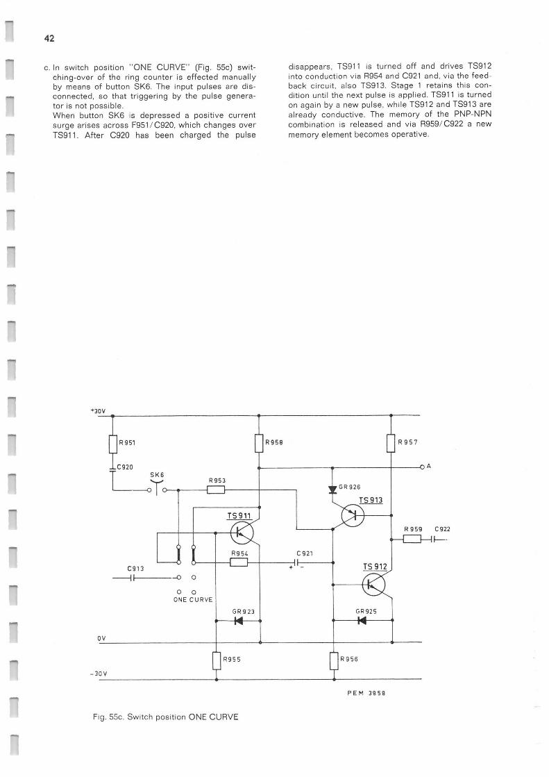
42
.~ c. ln switch position "ONE CURVE" (Fig. 55c) swit-
ching-over of the ring counter is effected manually by means of button SK6. The input pulses are dis-
.~. connected, so that triggering by the pulse genera-tor is not possible. When button SK6 is depressed a positive current surge arises across F951/C920, which changes over TS911. After C920 has been charged the pulse
i
i
~!
w w
w A A
'30V
1
disappears, TS911 is turned off and drives TS912 into conduction via R954 and C921 and, via the feed-back circuit, also TS913. Stage 1 retains this con-dition until the next pulse is applied. TS911 is turned on again by a new pulse, while TS912 and TS913 are already conductive. The memory of the PNP-NPN combination is released and via R959/C922 a new memory element becomes operative.
R 951
IC 920 SK6
R 953
~8 C913
-~ ~ -0 O
O O ONE CURVE
OV
R955
-30V
R958
R956
R957
R 959 C922
~'
Fig. 55c. Switch position ONE CURVE
PEM 3858

43
4. Amplifier (Fig. 56) The output signal of the step generator is present on the base of TS801. This transistor operates as an
-- impedance transformer which converts the step vol-tage into a constant step current of 100 µA per stage. Becauses the step signal —dependent on the function to be displayed —should be inverted, it is connected
"' direct to the base of TS804 by means of a relay (RE801), or to the base of TS802. This transistor forms an inverter stage for the step signal which is then again applied to the difference amplifier. Moreover,
"' the base potential of TS804 can be shifted within a certain range so that zero adjustment of the step signal is possible by means of control "ZERO". The base current of TS803 is varied by means of potentiometer R902. The collector of this transistor is connected to the base of TS804, so that the bias current at the input of the difference amplifier is thus determined.
_, The differential circuit with transistors TS804 and TS805 compares the step voltage across R810/R811 and R828 with the voltage on step switch R607 . . . 623 in the output circuit. The constant step voltage on
—. TS804, which can be adjusted with R811, serves as a reference. In case of a difference TS805, which recei-ves the drive signal via an impedance transformer,
i
.~
r
+r
i
R 632
t30V
drives the power amplifier so that the voltage is cor-rected in voltage divider R607. . .623 until the diffe-rence is eliminated. The step current adjusted with SK10 always remains constant independent of the resistance in the base circuit. When the transistor under test is not current but vol-tage-driven (with a constant voltage from step to step), voltage division is effected by the 200-mA current stage. The power amplifier in this case operates in the same way as with a constant current of 200 mA, whereby this current flows through 8623 (Fig. 57). Series resistors R601 . . .606 are included with SK10 II -F-I. The current from the 200-mA stage then causes a voltage drop across these resistors. In this way 6 voltage ranges are obtained for a step signal which can be selected by means of SK10. In case of voltage drive, series resistors R501 . . . R523 should be selected so that the voltage-drive characte-ristic is not lost. At high resistance values this pro-perty may be employed for current drive (e.g. 0.1 mV/ step 1 MS? = 0.1 µA/step). In switch position 0 resis-tors R501 . . . R523 can also be switched in so that characteristics can be displayed with resistance ter-mination of the base circuit (ICER)•
R 671
ZERO
RBJC
8905
R 025
_30V
TS 803
GR025 I RBOB
Fig. 56. Amplifier
R828
R 809
TS 80C
1 7_STEP
~R8!0
I I
+Vi
R 812
Rfi1G
R 813
_3CV
R816
PRE AMPL
TS 805
R P16
POWER
A MPL.
IMPEDANCE
TRANSFORMER
V2=RG_7_ST EP
1 SK 10
O~
R 607
O
R 623
O
7_STEP
PEM 3859
E

44
... 5. Power amplifier
As appears from the description under point 4, the ,_, current or voltage value of the step signal is deter-
mined by a difference amplifier. This difference am-plifier supplies the control signal for the power ampli-fier. The latter consists of pre-amplifier TS806, emitter-
..... follower TS807 and the final stage with TS808. . . TS811. TS808 and TS809 serve as a driver stage for the final stage with TS810 and TS811 which is a class AB push-pull output stage. Diodes GR801 and 802 provide the potential difference by which the d.c. set-ting of the output stage is determined. The output stage is supplied by a separate voltage source of +18 V/0/-18 V which is delivered by full-wave rec-
"' tifier GR1 and smoothed by C703 and C704.
C. DISPLAY SECTION
-- The display section serves for displaying the current and voltage relations in the transistor under test. By means of 2 mode and range switches, SK13 and SK16,
POWER AMPLIFIER
200 m A~ t
R 623
it is possible to select the horizontal and vertical deflection coefficients for displaying the characteris-tics and selecting the display method. The switches enable selection of various modes and moreover a position "EXT" has been provided for connection of an external signal.
Horizontal deflection (SK 13): The horizontal deflection determines the collector vol-tage in 15 ranges. The 3 upper ranges (100, 200 and 500 V/cm) serve for measuring breakdown voltages (H.T. source). These three voltage ranges can be reduced by a factor 10 with push-button x.1 (SK 13A); when this button is depressed, parallel resistor R385 is disconnected (Fig. 60). Switch position " serves for displaying the step signal whereby the range value selected with SK10 should be employed for reading the signal amplitude. For displaying the base voltage, e.g. as a function of IB, 4 ranges are available from 10. . . 100 mV/cm. External connection: 10 mV/cm, 1 MS2. Vertical deflection (SK16):
.II SKtO I n~V O ~ O 01000
R 601
O O
R 60 2
O O
R 603
p o'
R604
O O
R605
O O
R 606
Fig. 57. Voltage drive
500
200
100
50
20
PE M 3860

45
The vertical deflection operates in the same way as the horizontal deflection (SK13) and serves for range selection of the collector current. From 10 uA to 5 A/
—. cm the collector current can be sub-divided into 18 ranges. Moreover, it can be extended x0.5 and x5 in downward and upward direction. The sensitivity of the 10 lowest ranges can moreover
—' be increased by a factor 1000, so that the indications become nA/cm instead of f1A/cm. This sensitivity is only employed for leakage current measurements; changing over takes place by means of slide switch SK9. Switch position "~j" has the same function as with SK13, and the same applies to the base voltage
T3
T4
GRL
N
N GR3
SK12
1pMT, •~
O O
R<33
~ I ~ ~
R CL1
T G O
O
1O yA
and position "EXT". In this way different display methods are possible by means of SK14 and SK15.
1. Circuit for I, and V, •,.; measurements
The measuring circuit for displaying I, /V, i.; curves (as a function of the base current or voltage) is based on the diagram shown in Fig. 58. The collector-emitter voltage applied to the transistor under test is deter-mined by SK13 and applied to the c.r.t. via the hori-zontal amplifier. The measuring ranges can be selected by means of the voltage divider consisting of R332 . . . R344, and the corresponding step voltage is applied to one input of difference amplifier X.
VOLTAGE MEASUREMENT
c ~ O Q q . SK16~Y+YI
R LG: I '. ~ i RL 60
5A
SK161II
C URRE VT ME4GUR`tMEtiT
Fig. 58. Collector-current circuit
SA
PEM 3861
Trans~stcr under test

46
_.,
The other side of the difference amplifier is connected to attenuator 8346 . . . R357 which is also operated by
_ means of SK13. The combination of SK13/II and SK13/III enables accurate determination of the actual voltage present on the transistor by determining the loads presented by the resistors of SK13/II. Measure-
._ ment of the current flowing through the transistor is effected by means of range switch SK16/V+VI and the corresponding voltage divider. Resistors R442. . . R460 are the measuring resistors for the current stages. The step attenuator coupled with SK16/V-I-VI (III+IV) is only switched in for the "nA" ranges. The voltage drop across shunt resistors R442 . . . R460 is applied to difference amplifier Y via SK16/II or IV,
'^ one input of which is connected to the measuring potential and the other to earth U4/C5.
2. Circuit for VI;L measurements
For curve display, with VLL signal in the horizontal or vertical direction, e.g. I,_~ = f (V~;F;) or VI;L = f (VH~),the measurement is based on the principle shown in the
_ diagram of Fig. 59. The difference amplifiers for hori-zontal or vertical deflection are connected to the base-emitter circuit of the semi-conductor. The step signal from SK10 is determined by this amplifier and applied
i to the relevant attenuator. The desired display range
SK10
.—. _. —. J
DIFFERENT. .AMPL /1i~
SK 16~II ir ~ Y IN
— i
SK12 (—)
Transistor uMer test
GR2 GR<
GR1 GR3
R 3B<
R 381
R 1020
R1001
S K 16~III
Fig. 59. Measuring circuit for V13r measurement
can be selected by means of switch SK13/I or SK16/I. The corresponding voltage component then drives the output amplifier. The collector-emitter circuit is sup-plied by the half-wave voltage obtained from TS -I-T4 and GR1 . . . 4.
3. Circuit for breakdown voltage and leakage current measurements (Fig. 60).
Fos testing 2-pole semi-conductors as regards break-down voltage or leakage current, ahalf-wave voltage is generated by means of continuously variable trans-former T1, H.T. transformer T1101 and GR1101 and 1102. This voltage is applied to socket BU5 via switch con-tact DS1. Voltage measurement is effected by means of the voltage divider consisting of resistors R1101 . . . 1103 and R329. . .331. By means of switch SK13/II one of the three voltage stages is applied to the horizontal amplifier. Via socket BU4 the current through the semiconduc-tor is determined. This measuring circuit is connected to earth via step switch SK16/IV, II, R433. . . R441 and R442 . . . R450. The voltage arising across the resistance selected with range switch SK16 is applied to the input of the verti-
T3
TG
S K 13~I
—o
l\ I FINAL
J AMPL x
10 mV
20mV
60mV I
S K 16~I
100mV —O ,
R ~B
L28
O 20mV
O SOmV
O 100 mV
C~ 200 m V
R L32
PEM 3862
FINAL AMPL. Y

A A A
A A
A A 1 1 A A A A A A A A R
cal amplifier and thus to the vertical deflection of the c. r.t. Slide switch SK9 for switching on the h.t. generetor, moreover serves for changing over from µA to nA ranges. ln position "f~A" of SK9 resistors 8442 . . . R450 are included, and in position "nA" R433 . . . R441 are moreover included in series with R442 . . . R450. De-pendent on the selected range a voltage drop will arise across the included resistors which is proportional to the leakage current flowing through the semiconduc-tor under test.
4. Difference amplifier for X and Y deflection
The preset drive signal is amplified or changed by the semi-conductor under test. This signal is applied to the X and Y amplifiers dependent on the selected mode
i
RS GRp GR1 RG DS1
GK13/II
T 1101 R329
BUS
O
R1... R3
100V~
47
and range, which apply proportional voltages to the horizontal and vertical deflection units of the c.r.t. Theses output signals are determined and amplified by 2 independent difference amplifiers. The following description applies to the X amplifier which functions identically to the Y amplifier. The input stage consists of two field-effect transistors which operate as impedance transformer and ampli-fier. The input signal is applied to the first gate and the second gate serves for adjusting the d.c. balance with R303 or R319. The working points of these transistors are automatically adjusted by means of TS303 and TS304 which are controlled by the constant voltage drop on zener diodes GR304 and 305 in case of a varying drain current. The output signal on the drain connection of TS301
x•1 S KtI A
R 365
BUG
(—)
SK16
~J
R
SK9 ~
p — nA
■_ _ NA
-- off
IY SKi6/II
CG2
456
t0 y4 honA)
r Y_AMPLI FIER
I ~
~
~
I I ~ I
IOmA 1 (tOy A)
I 5K16/Y.YI
tOy A(tOn A)
~ ■ tOmA (tOy A)
R 457---R460
Fig. 60. Measuring circuit for breakdown-voltage and leakage-current measurements
r X _AMPLI FIER
I
I_ 1
PEM 3863
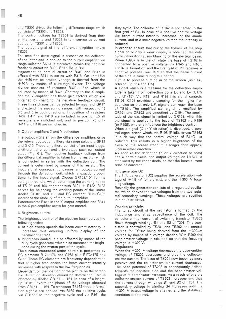
48
and TS306 drives the following difference stage which consists of TS302 and TS305. The control voltage for TS304 is derived from their
_, emitter currents and TS304 in turn serves as current source for TS301 and TS306. The output signal of the difference amplifier drives TS307. The amplified drive signal is present on the collector of the latter and is applied to the output amplifier via range selector SK13. It moreover closes the negative feedback circuit via R322, 8317, R310, R34.
~— Adjustment as parallel circuit to R310 and R317 is effected with R311 in series with 8318. On unit U3A the +50 mV calibration voltage is derived from the +30 V by means of a voltage divider. The voltage
'~ divider consists of resistors R370. . .372 which is adjusted by means of R373. Contrary to the X ampli-fier the Y amplifier has three gain factors which are obtained by changing the negative feedback circuit. These three chages can be selected by means of SK17 and extend the measuring ranges (with respect to 1) 0.5 and 5 in both directions. In position x1 resistors R407, R411 and R418 are included, in position x5 all resistors are switched out, and in position x5 only R411 and 8418 are switched in.
„~ 5. Output amplifiers X and Y deflection
The output signals from the difference amplifiers drive the relevant output amplifiers via range selectors SK13 and SK16. These amplifiers consist of an input stage,
'~ a differential circuit and atwo-stage push-pull output stage (Fig. 61). The negative feedback voltage from the differential amplifier is taken from a resistor which is connected in series with the deflection coil. The current is determined by means of this resistor. The input signal consequently causes an output current through the deflection coil, which is exactly propor-
,~ tional to the input signal. Diodes GR103/104 form a voltage threshold, which determines the working points of TS105 and 106, together with R121 + R122. R188 serves for balancing the working points of the limiter diodes GR101 and 102 and RC element R110/C102 increases the stability of the output amplifier. Potentiometer 8157 in the Y output amplifier and R311 in the Xpre-amplifier serve for gain control.
6. Brightness control
The brightness control of the electron beam serves the following tasks:
"" a. At high sweep speeds the beam current intensity is increased thus ensuring uniform display of the oscilloscope trace.
b. Brightness control is also effected by means of the duty cycle generator which also increases the bright-ness during the written part of the cycle.
The function mentioned under point a is performed by ,r RC elements R174/176 and C162 plus R173/175 and
C163. These RC elements are frequency dependent so that at higher frequencies the beam current intensity increases with respect to the low frequencies. Dependent on the position of the picture on the screen the deflection direction should be determined. This is effected by diodes GR161 . . . 164. In case of a bright-up TS161 inverts the phase of the voltage obtained from GR161 . . . 164. To transistor TS162 three informa-tion signals are applied: via R169 the positive cycle, via GR163/ 164 the negative cycle and via R161 the
duty cycle. The collector of TS162 is connected to the first grid of B1. In case of a positive control voltage the beam current intensity increases, or the anode current, and at a more negative voltage the intensity is reduced. In order to ensure that during the flyback of the step signal no or only a weak display is obtained, the duty cycle generator causes blanking of the electron beam. When TS907 is in the off state the base of TS162 is connected to a positive voltage via R945 and R161. TS162 is turned off and the first grid of B1 receives a negative potential via R163 so that the beam current of the c.r.t. is small during this period. Circuit to prevent burning in of the screen (unit 1A; refer to Fig. 114 and 115) A signal which is a measure for the deflection ampli-tude is taken from deflection coils Lx and Ly (U1/5 and U1/18). Via R191 and R192 this signal controls TS191. C191 provides a damping for the higher fre-quencies so that only L.F. signals can reach the base of TS191. The amplified a.c. signal is rectified by GR191 and GR192 and smoothed by C194. The ampli-tude of the d.c. signal is limited by GR193. After this the signal is applied to the base of TS162 via R196 (or R195), where it influences the brightness control. When a signal (X or Y direction) is displayed, a con-trol signal arises which, via R196 (R195), drives TS162 in such way that the control voltage of B1/G1 is reduced. This results in a higher brightness of the trace on the screen when it is longer than approx. 3 cm in either direction. As soon as the deflection (X or Y direction or both) has a certain value, the output voltage on U1A/1 is stabilised by the zener diode, so that the beam current remains constant.
H.T. generator U2 The H.T. generator (U2) supplies the acceleration vol-tage of +4.5 kV for the c.r.t. and the +300—V focu-sing voltage. Basically the generator consists of a regulated oscilla-tor, which derives the two voltages from the two isola-ted secondary windings. These voltages are rectified in a doubler circuit.
Working principle: The tuned circuit of the oscillator is formed by the inductance and stray capacitance of the coil. The collector-emitter current of switching transistor TS203 flows through windings S1 and S2 of T201. This tran-sistor is controlled by TS201 and TS202, the control voltage for TS202 being derived from the +300—V voltage by means of a voltage divider. With R209 the base-emitter voltage is adjusted so that the focusing voltage is +300 V. Regulation: When the +300—V voltage decreases the base-emitter voltage of TS202 decreases and thus the collector-emitter current. The base of TS201 now becomes more positive and the collector-emitter current decreases. The base potential of TS203 is consequently shifted towards the negative side and the base-emitter vol-tage of this transistor increases. As a result of this the collector-emitter current of TS203 increases and thus the current through windings S1 and S2 of T201. The secondary voltage in winding S4 increases until the +300—V output voltage is attained and the stabilised condition is obtained.

49
IX. Disassembly
CAUTION
In this instrument high tensions of 500 Vp, 3 kVp and 4.5 kVp are generated. Therefore due care should be
"" taken when working on a switched-on instrument.
A. CABINET
Top panel: Loosen the two upper screws at the rear of the instru-ment (Fig. 3) by giving them a quarter turn. The panel can then be slid out to the rear. Bottom panel: Remove the corresponding screws from the bottom plate and remove the tilting bracket by pressing the
,... ends of the bracket together.
A A A A A
430V
INPUT
R lOC
R105
TS 102
T5101
_30V
Ov
= GRtOt R12
R7J6
GR102
R 108
R 112
R 11,
T R 113
R 11G
Rear panel: First remove the top and bottom panels, then remove the three screws on each side. Unsolder the earthing connection or unscrew the soldering tag, if the rear panel should be completely removed. Remove the 4 fixing screws; the panel can then be taken out.
B. CRT
The CRT should be replaced with due care so that undesired mechanical tensions are avoided. It should, moreover, be taken into account that the external dimensions of the CRT may very. Therefore, when replacing the tube strictly adhere to the following instructions. Removing the CRT: — Remove the top, bottom and side plates as well as
the rear panel. — Puil out the tube socket and detach the EHT cable
from the tube by slightly compressing the clips.
I C,02
R110 TS104
GR104
R 115
T5105
Fig. 61. X-Power amplifier
I
~R105 ~GR105
1
R tt9
R 120
GR 103
+lev
T^106 ;
123
~f VOKE
R "'9
TS 1602
PEM 3864
18V
OV

~ so
~.
A A A A
A A w A
w A A
A A A
— Remove the bezel (romove the 4 knurled nuts). —Remove the screw of the bracket at the rear of the
deflection unit. —Slightly loosen the 4 nuts on the threaded studs (on
which the bezel was fitted) at the front of the in-strument (do not remove them).
— Loosen screw M (Fig. 62) until the tensioning strip is loose.
—The tube can now be removed in forward direction after carefully pushing it out of the corner pieces. For fitting a new tube it is advisable to completely remove the deflection unit:
Removing the deflection unit: —Unsolder the connection wires of the deflection coil
at the relevant soldering tags.
IMPORTANT:
Before unsoldering first make a note of the wire colours to prevent interchanging.
— Remove the two fixing screws L (Fig. 62) and take out the complete holder with deflection unit.
—Remove screw K (Fig. 63).
U2 (unit slid out and lid R209 removed)
Fig. 62. Side view (left)
R359
Mounting the deflection unit on the picture tube: —Slide the deflection unit on the tube neck in the
correct position (the screw of bracket down; the correction magnets should be situated on the broad side of the tube).
—Slide the mumetal jacket about 5 mm into the deflec-tion unit.
— Push the deflection coil on the tube, align it and slightly tighten screw K (so that the tube can still be turned in the unit).
Mounting the CRT:
— Push the tube into the cornerpieces, mind the correct position. It should be possible to shift the 4 cornerpieces. The rubber supports should be correctly positioned.
— Fit the tensioning strip but do not yet tighten the screw.
—Slightly tighten the four nuts on the threaded studs so that the cornerpieces can still be shifted.
— Position the tube symmetrically in the front frame; the screen should be flush with the front plate.
—Tighten screw M of the tensioning strip (Fig. 62).
A

51
— Re-align the tube with respect to the front frame and completetly tighten the four nuts of the threaded studs (the screen should now be exactly flush with the front plate).
— Fit the yoke holder, by means of the two screws L (Fig. 62) and make sure that the plexiglass support properly fits against the yoke.
— Align the plexiglass support in the centre position and fix it by means of screw G (Fig. 62).
—Tension the plexiglass support as much as possible.
Accurately align the yoke; it should be slid forward as far as possible. Secure the bracket on the plexiglass support with screw G (Fig. 62). The springs should now press the yolke against the picture tube.
— Connect the deflection unit (mind the colours of the wires), fit the tube socket and the EHT connection.
— Fit the bezel. — Adjust the yoke and the picture tube according to
the instructions of chapter XI.F.2.
Fig. 63. Top view

A
A
A
A
A A
A
...
'"1
A
52
C. REMOVING THE SUB-UNITS
When removing the sub-units be careful when solde-ring connection wires and short connections. Make sure that no wires are interchanged or skipped. Make a wiring list and note the wire colours!
1. Unit U1
This unit is located at the rear of the instrument and is easily accessible after removal of the rear panel.
T2
Fig. 64. Bottom view
T3 T4
2. Unit U2 (Fig. 65)
Remove the left-hand side panel and loosen 2 screws E (Fig. 64). The cover can now be removed and the EHT unit can be pulled out.
SK13 PEM 4045
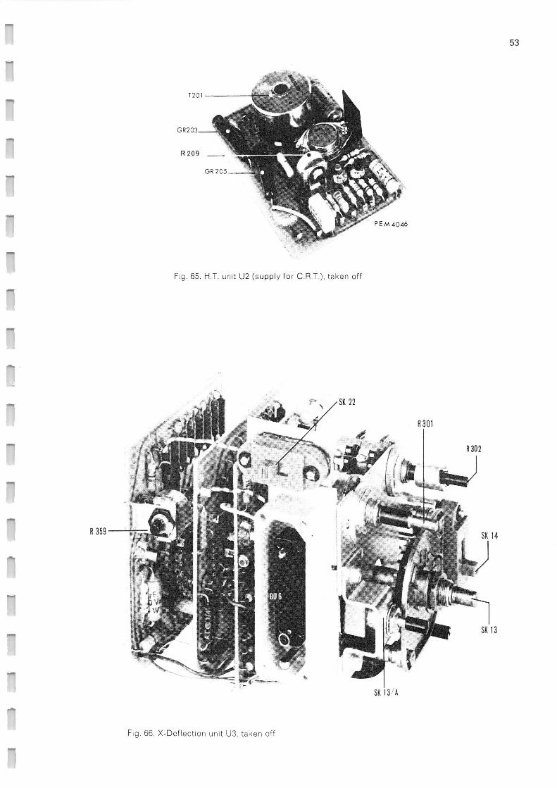
53
R 359
T201
GR203
R 209
Fig. 65. H.T. unit U2 (supply for C.R.T.), taken off
Fig. 66. X-Deflection unit U3, taken off
SK 13'A
R301
R 30 2
SK 14
SK 13

54
Rd01 SK16
1~•
D
Fig. 67. Y-Deflection unit U4, taken off
SK 2
Fig. 68. Base-resistor unit U5, taken off
PEM 4049

55
SK l0A
R 631
Fig. 69. Shunt unit U6, taken off
RE 801
R802
R 811
U8A
U8B
PEM4047
R 833
Fig. 70. Final-amplifier unit U8, taken off

A
1
A A
A A
A
A
A
A
56
3. Units U3, U4, U5 and U6 (Fig. 66, 67, 68, 69)
These units are centrally fixed. Remove the knobs, loosen the central fixing nuts, and unsolder the rele-vant connection wires. Remove the bottom plate, the top plate and, if ne-cessary, the left-hand side panel.
4. Unit U7
Remove the rear panel. The unit is then readily accessible (4 fixing screws).
5. Unit U8 (Fig. 70)
Remove the rear panel. Remove 2 screws N (Fig. 63) and loosen 2 screws O. Unsolder the connection wires. When the unit is slightly pushed down, the screws can be removed from the bayonet holes.
6. Unit U9 (Fig. 72)
Remove the top plate, and then remove unit U5. Remove the knobs, the fixing nuts of SK3, SK8 and R902 as well as the knurled nut of SK6. Remove screw P (Fig. 63) and loosen screw Q (Fig. 71). Unsolder the wires, slide the unit backwards and take it out.
t7'v
f
Fig. 71. Side view right
u
7. Unit U10 (Fig. 74)
Remove the bottom plate, the top plate and the rear panel. Loosen fixing nut R (Fig. 73) and pull out the spindle and knob of T1. Loosen the spindle coupling of SK12 (accessible frcm the top) and pull out the spindle. Remove the two screws T (Fig. 63) at the base plate of U10 and loosen screws S (Fig. 63). Unsolder the con-nection wires and lift out the units.
8. Unit U11 (Fig. 75)
Remove the top plate and the left-hand side plate. Remove three screws U (Fig. 71) as well as screws S (Fig. 63) and take out the angle support. Remove the two screws V (Fig. 71) the EHT unit can now be taken out.
9. Unit U12 (Fig. 76)
Remove the bottom plate and unscrew the knurled nut of SK18. The complete socket and switch unit can now be removed.
Remove the top plate. Loosen. the fixing clips and take out the printed circuit board.
PEM4050
A

57
D. REMOVING COMPONENTS
If components are to be replaced which are located in one of the sub-units, it will generally be necessary to disassemble the relevant unit. The components can then be easily replaced.
1. Variable transformer T1
Remove the top-panel, the cover-plate of the mains-fuses and loosen the mounting plate which has been fitted with the three screws. Remove screws Y
.-. (Fig. 63). Loosen tightening nut R (Fig. 73) and pull out the spindle of T1. Unsolder the connection wires of T1. Loosen the two hexagon screws W (Fig. 63) by means of a spanner (7 mm). The transformer can now
r
~..
U 96
Fig. 72. Step generator U9, taken off
be slightly pushed up and the screws can be removed through the bayonet holes, after which the transformer can be lifted out of the instrument. Before mounting the new transformer, fit the soldering tags and remove the stopping cams on the front of the transformer. The front of the transformer should be fitted completely against the mounting plate.
2. Push-button units SK4 (Fig. 77)
Remove the top plate. Remove the two screws at the side of the push-button unit and unsolder the connec-tion cables.
3. Push-button unit SK19 (Fig. 77)
Remove the bottom plate. Remove the fixing screws on either side and also remove screw X (Fig. 64).
SK 1
SK 3
SK 8
R 901
SK 7
SK 6
R 902
SK 11

58
...,
A A A
r
l
Fig. 73. Rear view (rear panel taken off)
SK 12 Fig. 74. Collector-load unit U10, taken off
0 0
x a
~o~ o~ Q ,moo
Q
n

59
4. Pilot lamp LA1
Remove the right-hand side panel (Fig. 71). Pull out the "' lamp holder in backward direction.
The lamp can now be easily replaced (screw fitting E10, voltage 6 V).
_ Pilot lamps LA2 and LA3. Remove the bezel and the measuring lattice.
CONTACT DSl
DS1 GUS BU4
GRI101
Fig. 75. H.T. unit U11 (3 kV). taken off
The lamps can then be replaced. Bayonet sockets BA7s, voltage 6 V.
5. Switch knobs
The round switch knobs can be removed by carefully prizing off the cap with a knife and loosening the nut of the clamping cone. The knob can then be pulled off the spindle.
SK9 PEM 4052
U11 3KV
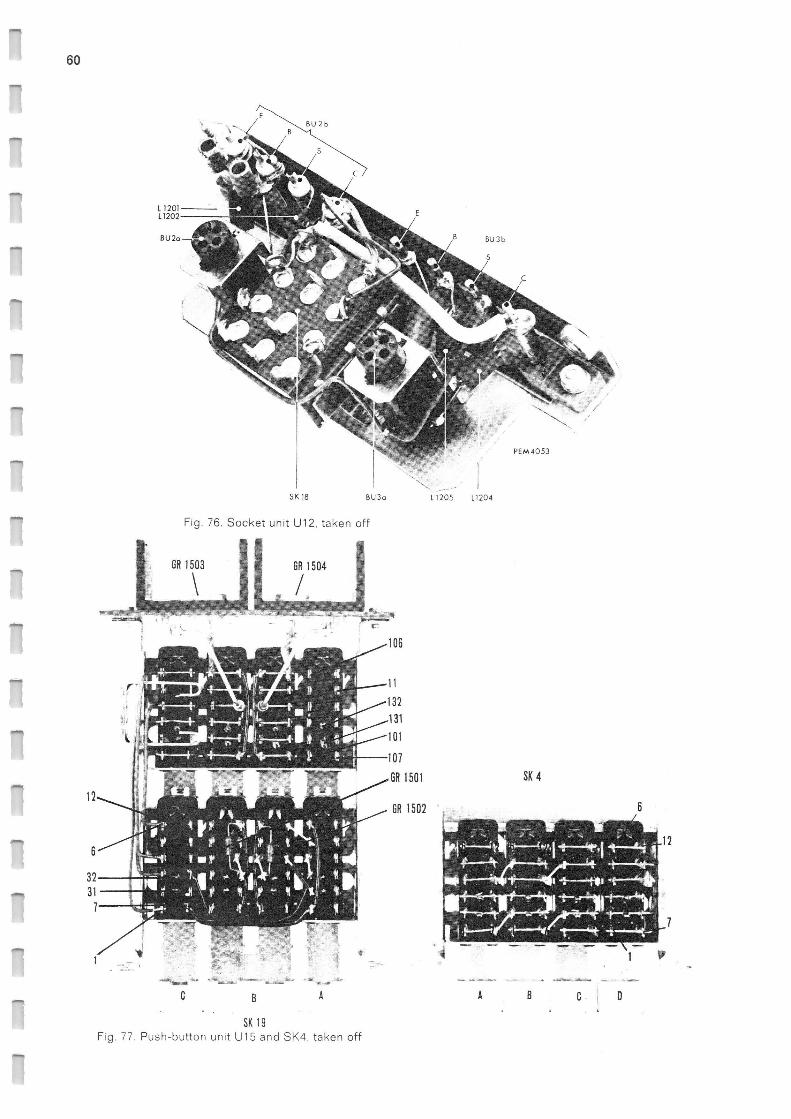
60
w
1F~
A
L 1201 11202
BU2a
SK 18 BU3a
Fig. 76. Socket unit U12, taken off
OR 1503 OR 1504
B A
SK 19 Fig. 77. Push-button unit U15 and SK4, taken off
132
131
101
107
GR 150i
L1205 L 1204
A
SK 4
B C D
A

61
X. Maintenance --- Transistor curve tracer PM 6507 has no components
which are actually subject to wear; therefore, the measuring instrument requires practically no mainte-nance.
However, to ensure trouble-free operation the instru-ment should not be exposed to excessive heat, mois-ture or dust. The perforations in the top plate should not be covered because otherwise the natural cooling will be impeded.
CAUTION:
Do not set the brightness to an unnecessarily high value. In case of continuous operation and a stationary image, the brightness should be kept as low as possible.
Avoid spots of high intensity to prevent burning in of the picture tube. A few hints in the event of faults. Due to the great number of controls and switching possibilities aperating errors are likely to occur. It is advisable to first check the switch settings. Further instructions ar regards the relevant mode of operation are given in the directions for use. In case of a fault it is always possible to consult the local service organisation.
CAUTIONI
When carrying out measurements on an opened in-strument be extremely careful to avoid short-circuits; in view of the ENT source only use insulated tools and clips!
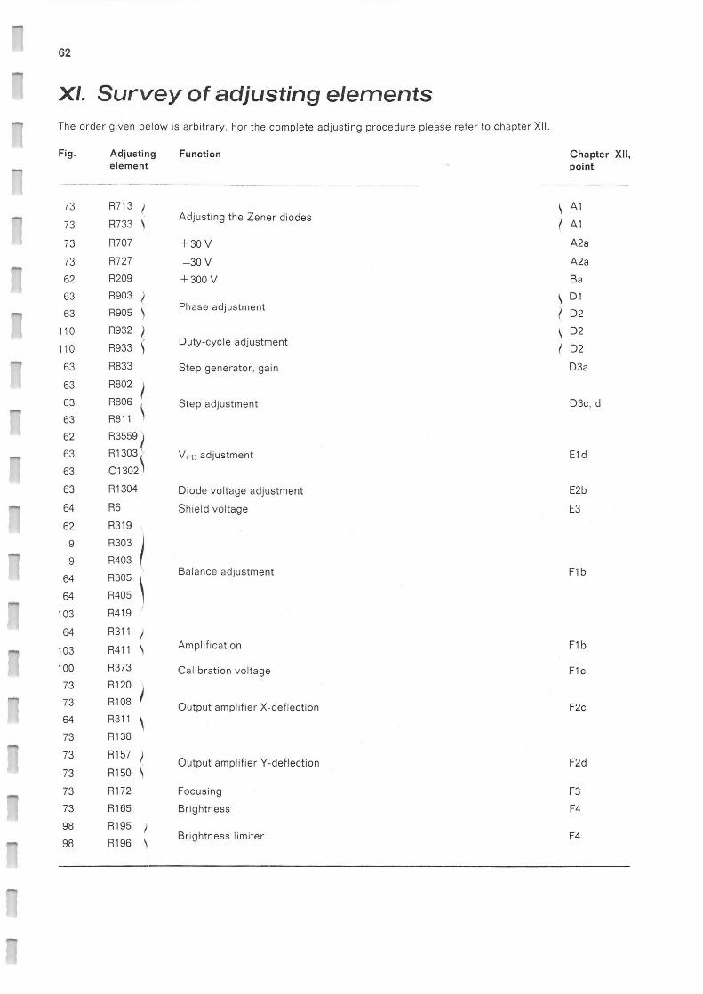
s2
r r A
...
X1. Survey of adjusting elements The order given below is arbitrary. For the complete adjusting procedure please refer to chapter XII.
Fig.
73
73
73
73
62
63
63
110
110
63
63
63
63
62
63
63
63
64
62
9
g
64
64
103 8419
64 8311 r
103 8411 ~ Amplification F1 b
100 8373 Calibration voltage F1c 73 8120
73 8108 Output amplifier X-deflection F2c 64 8311 1
73 8138
73 8157 1 Output amplifier Y-deflection F2d 73 8150 ~
73 8172 Focusing F3
73 8165 Brightness F4
98 8195 ~
Adjusting element
Function Chapter XII, point
8713 f 1 Al
8733 ~ Adjusting the Zener diodes
r Al
8707 -F 30 V Ala
8727 —30 V Ala
8209 -1- 300 V Ba
8903 ~ ~ D1
8905 ~ Phase adjustment j D2
8932 1 ~ D2
8933 y Duty-cycle adjustment j D2
8833 Step generator, gain D3a
8802 )
8806 Step adjustment D3c, d 8811 1
83559
81303 V, ~.: adjustment E1d
C1302~
81304 Diode voltage adjustment E2b
R6 Shield voltage E3
8319
8303 I
8403
8305 Balance adjustment F1 b
8405 I
98 8196 tiBrightness limiter F4
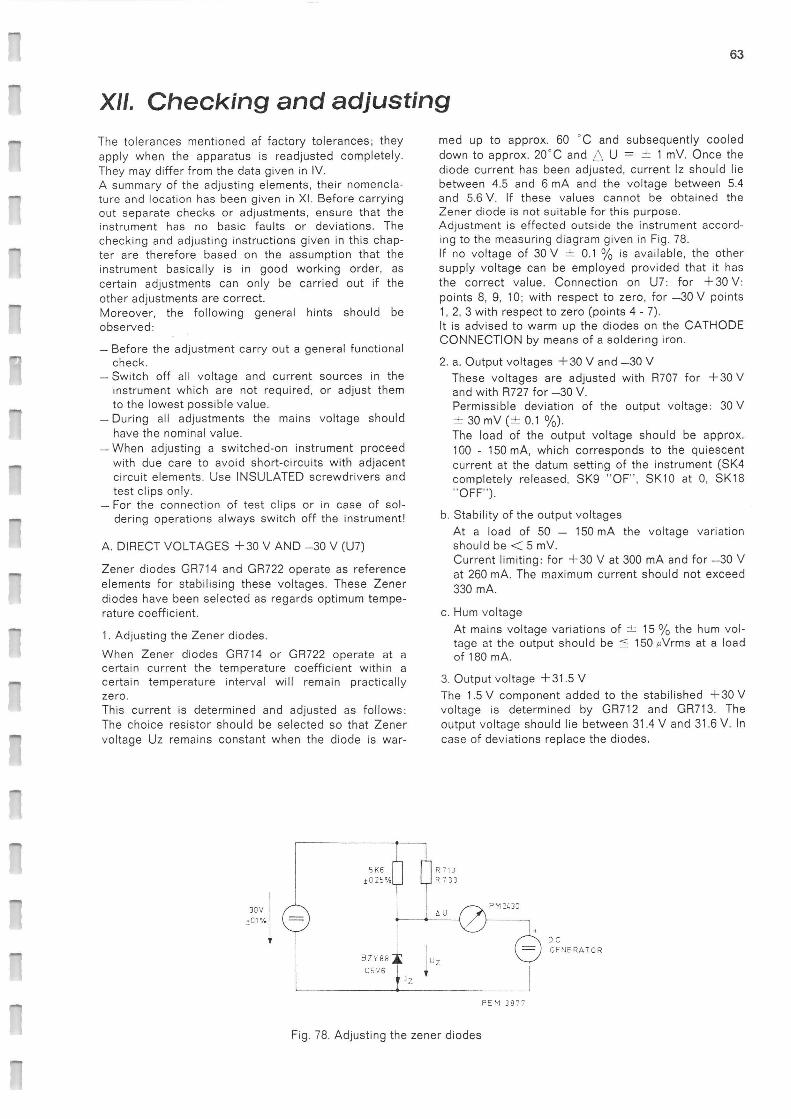
63
X11. Checking and adjusting
-- The tolerances mentioned of factory tolerances; they apply when the apparatus is readjusted completely. They may differ from the data given in IV. A summary of the adjusting elements, their nomencfa-
"' ture and location has been given in XI. Before carrying out separate checks or adjustments, ensure that the instrument has no basic faults or deviations. The checking and adjusting instructions given in this chap-
- ter are therefore based on the assumption that the instrument basically is in good working order, as certain adjustments can only be carried out if the other adjustments are correct. Moreover, the following general hints should be observed:
— Before the adjustment carry out a general functional "~' check.
— Switch off all voltage and current sources in the instrument which are not required, or adjust them to the lowest possible value.
—During all adjustments the mains voltage should have the nominal value.
—When adjusting aswitched-on instrument proceed „_, with due care to avoid short-circuits with adjacent
circuit elements. Use INSULATED screwdrivers and test clips only.
— For the connection of test clips or in case of sol--. Bering operations always switch off the instrument!
A. DIRECT VOLTAGES +30 V AND —30 V (U7)
,,,,_ Zener diodes GR714 and GR722 operate as reference elements for stabilising these voltages. These Zener diodes have been selected as regards optimum tempe-rature coefficient.
1. Adjusting the Zener diodes.
When Zener diodes GR714 or GR722 operate at a certain current the temperature coefficient within a certain temperature interval will remain practically zero. This current is determined and adjusted as follows: The choice resistor should be selected so that Zener
"' voltage Uz remains constant when the diode is war-
30V
+C1
med up to approx. 60 °C and subsequently cooled down to approx. 20°C and Q U = = 1 mV. Once the diode current has been adjusted, current Iz should lie between 4.5 and 6 mA and the voltage between 5.4 and 5.6 V. If these values cannot be obtained the Zener diode is not suitable for this purpose. Adjustment is effected outside the instrument accord-ing to the measuring diagram given in Fig. 78. If no voltage of 30 V ± 0.1 % is available, the other supply voltage can be employed provided that it has the correct value. Connection on U7: for +30 V: points 8, 9, 10; with respect to zero, for —30 V points 1, 2, 3 with respect to zero (points 4 - 7). It is advised to warm up the diodes on the CATHODE CONNECTION by means of a soldering iron.
2. a. Output voltages +30 V and —30 V These voltages are adjusted with R707 for +30 V and with R727 for —30 V. Permissible deviation of the output voltage: 30 V
The load of the output voltage should be approx. 100 - 150 mA, which corresponds to the quiescent current at the datum setting of the instrument (SK4 completely released, SK9 "OF", SK10 at 0, SK18 "OFF").
b. Stability of the output voltages At a load of 50 — 150 mA the voltage variation should be < 5 mV. Current limiting: for -I-30 V at 300 mA and for —30 V at 260 mA. The maximum current should not exceed 330 mA.
c. Hum voltage At mains voltage variations of -±- 15 %the hum vol-tage at the output should be ~_ 150 uVrms at a load of 180 mA.
3. Output voltage ~-31.5 V The 1.5 V component added to the stabilished +30 V voltage is determined by GR712 and GR713. The output voltage should lie between 31.4 V and 31.6 V. In case of deviations replace the diodes.
SK6 f025
Fig. 78. Adjusting the zener diodes
PEM 38'7
CC GENERATOR
64
B. EHT UNIT 4.5 kV (U2)
a. Adjust the -1-300 V voltage with R209 average -- brightness.
b. Check the 4.5 kV voltage by means of HT probe GM 6071 and d.c. voltmeter GM 6020, PM 2440 or
_ PM 2430. Input resistance of the voltmeter 100 Mn. Load resistance of the EHT circuit > 200 MS?. Nomi-nal value: 4500 V = 200 V.
-- C. 3 kV VOLTAGE FOR TESTING DIODES (U11)
Half-wave voltage adjustable with T1, max. value at nominal mains voltage approx. 3 kV.
-- Visual check on CRT: SK13 at 500 V, SK9 at ~~A or nA, Slowly turn T1 fully clockwise. The voltage curve on
"~" the screen will then be 6 cm for 3 kV.
D. STEP GENERATOR (U9)
1. Phase adjustment of the trigger pulses Phase adjustment of the trigger points can be effected by using a transistor as test object and observing the characteristics on the screen of the CRT
1st Phase
,_ —Depress the 10 V button of SK4. — Set T1 (V, ,.;) to mid position (e.g. 5 V). —SK8 at 2.5 %duty cycle. — SK13 at 1 V/cm. ._.. —Set SK16 at a high sensitivity so that accurate
adjustment is possible.
— Set SK1 at "100 from 0".
—" —SK7 at "REP FAM". —SK3 at 8. —Adjust the intersection point of the curves to zero
_.. or minimum by means of R903.
2nd Phase
^- Initial setting as above, however: — SK1 at "100 to 0".
— With R905 adjust the trigger point to max. reversing point.
2. Duty-cycle adjustment 2.5. . .60 % -h 100%
T —Initial setting of instrument: use a transistor as test object and display a set of curves with SK7 at "REP. FAM".
—Turn SK8 fully clockwise (switch in the locked .~.. position).The mark on the knob should point towards
the centre of position 100 %.
—Connect an oscilloscope to U9A/3. —Set SK8 (R901) at position 2.5 %.
The duty cycle phase should now be 250 µs ± 10 us. —Adjustment is effected with R933 (for this, unit U9
must be removed). --- —Set SK8 at 60 %.
The duty cycle phase should now be 6 ms -~ 250 µs. —Adjustment is effected with R932.
3. Adjusting the amplifier (U8)
a. Adjustment of potentiometer "ZERO"
— Connect a resistor of 100 S2 --- 0.2 % to sockets B and E.
— SK1 at "100 from 0". —SK3 at 8. —SK7 at "ONE CURVE". —SK8 at 100 %. — SK10 at 1 mA. — R902 at the centre of its control range (mark under
"ZERO"). — SK19: all buttons released. — Connect a microvoltmeter or digital voltmeter to
the external 100 S2 resistor. —Adjust potentiometer R833 until the output cur-
rent is 0 -~- 10 ~A (~ ± 1 mV3. If this is not possi-ble replace TS814.
—This tolerance should also be maintained if button SK19A is depressed.
b. Adjustment of the negative deflection
Setting as under a, however:
— Set SK3 at 2 . . . 7. —Set SK7 at "One Curve". —Adjust potentiometer R811 so that the current per step is 1 mA for steps 2. . .7 (SK3). Adjust the 1st step (SK3 at 2) by means of R802.
These adjustments should be carried out very accurately (-± 1 % per step or 0.1 V -±- 1 mV across the 100 52 resistor connected to B-E).
c. Adjustment of the positive deflection Setting as under b, however: — SK19A: depressed. —Adjust potentiometer R806 so that the current per
step is 1 mA for steps 1 - 8 (SK3); (tolerance ~-1 % or 0.1 V ± 1 mV across the 100 n resistor connected to B-E).
E. COLLECTOR VOLTAGE SUPPLY
1. Voltage ranges 10 Vp, 50 Vp, 100 Vp, 500 Vp
a. Range 0 - 10 Vp
— SK4A (10 V) depressed. — SK13 at 2 V/cm. — SK16 at 5 A/cm. — SK18 at TS1. —Turn T1 clockwise and check the X-deflection on
the picture screen. Adjustment: 10 V = 5 cm screen distance.
— Connect an oscilloscope to BU2b C (high) and E (low) and check that both halfwaves are present.
— Connect a resistor or 1 n, 100W to BU2b, C and E. —The trace should be deflected in the vertical
direction over approx. 2 cm (2 cm = 10 A), accor-ding to Fig. 79 (the collector voltage source is not stabilished). Short-circuit C-E (R~~ = 0.5 S2), V~~~.; = 10 Vp, i~ _ 20 Ap. After approx. 20 - 25 sec thermal switch SK5 should cut out.
—Hum on the picture tube (Fig. 80): Short-circuit C-E (R,~ = 0.5 S2), V~ L; = 10 Vp, I~~ _ 20 Ap. SK13 at 1 V/cm.

65
b. Range 0 - 50 Vp
— SK4 B depressed. — SK13 at 10 V/cm. — SK16 at 1 A/cm. — Connect a resistor of 10 S?, 100 W to BU2b C-E. —Set SK18 at TS1.
„_, —Adjust V, ~; to 50 V with T1 (5 cm). — I, should be approx. 3,6 A (? 3,6 cm).
c. Range 0 - 100 Vp
—' — SK4 C depressed. — SK13 at 20 Vlcm. — SK16 at 500 mA/cm. — Connect a resistor of 50 2, 100 W to BU2b, C-E.
` —Set SK18 at TS1. —Adjust the V,~~; to 100 V with T1 (5 cm). — I, should be approx. 1.6 A (? 3.2 cm).
d. Range 0 - 500 Vp
— Depress SK4 D. — SK13 at 50 V/cm.
"' — SK16 at 50 mA/cm. — Connect a resistor of 2 kn, 100 W to BU2, C.E. —Set SK18 at TS1. —Adjust the V, ~; to 500 V with T1 (10 cm).
'— — I, should be approx. 0.2 A (?_ 4 cm). Adjustment at smaller currents: — SK13 at 50 V/cm. — SK16 at 10µA/cm. —Adjust V, ~.; to 400 V with T1 (8 cm). — By means of 81303 and C1302 reduce the angle
enclosed by the diverging lines and make the two ._„ traces coincide. Adjust 8359 until the loop as
closely as possible approximates a straight line. After the adjustment the trace should fit inside a rectangle of max. 7 mm height (7 µA p-p) and a
—, width of 8 cm (400 V).
_.,
2. High tension for testing diodes
a. µA ranges
—None of the buttons of SK4 depressed. —SK9 at "µA". — SK13 at 500 V/cm. — SK14 at "INNERS". — SK15 at "NORMAL". — SK16 at 10 µA/cm. — SK17 at "x0.5". —Depress DS1. —Turn T1 clockwise until a horizontal line of 4 cm is
obtained on the screen, corresponding to a vol-tage of 2,000 Vp.
Fig. 79. Adjusting the collector-voltage source 0-10 V
b. nA ranges
—None of the buttons of SK4 depressed. — SK6 at "SINGLE FAM". —SK9 "nA". — SK10 at 1µA/step. — SK11 at "GROUNDED". — SK16 at 10 nA/cm. — SK17 at "x0.5". —Turn R1 fully counter-clockwise. —Depress DS1. — Adjust the picture horizontally with 81304. The
loop should be smaller than 6 mm (3 nA). Ensure that the instrument is earthed.
3. S control voltage
— Set SK20 at — (~-). —Turn R1 fully clockwise. —The voltage on sockets S-E of BU2 (BU3) should be
10 V ~- 0.1 V (adjust by replacing R6). — Repeat the check for the other polarity -F (—). —Check of ,with SK20 at : S.E = 0 V.
F. MONITOR
1. Pre-amplifiers U3 A, and U4 A
Checking and adjusting of the amplifiers can be effec-ted independent of the step signal and the collector circuit by switching the instrument to external opera-tion and by applying asine-wave voltage of approx. 200 Hz to the sockets on the left of the instrument. The adjustment is the same for the horizontal and vertical pre-amplifiers except for the expansion switch on unit U4. In the following description the indications in brackets refer to U4 A and the other indications to U3 A.
a. Checking the input stages as regards gate leakage current
With this check it should be observed that the leakage current of protection diodes GR301/GR302 The diodes should therefore be unsoldered. If the leakage current of a FET is too high, both transistors in the relevant stage should be replaced because they have been selected in pairs (for the ordering code, see list of electrical parts). — Connect a resistor of 1 M2 ± 5 % to sockets B
and H of BU6 (on the left-hand side of the in-strument).
—Set switches SK13 and SK16 at "EXT". —All buttons of SK4 should be released and T1
should be turned fully counter-clockwise.
Y=4cm
X
X:O.Q mm
Fig. 80. Hum influence on the C.R.T.
66
— A small loop is now displayed on the screen. This trace should be adjusted to the centre of the screen at low brightness.
X-inputs:
— Short-circuit sockets D and H of BU6. ,_ —The loop should not shift more than -+- 3 mm in the
horizontal direction (an angular shift of the loop does not affect this check).
— Short-circuit sockets M and H of BU6. —. —Max. deviation in the horizontal direction -~- 3 mm.
Y-inputs:
— Short-circuit sockets E and H. —` —Max. deviation in vertical direction ± 3 mm.
— Short-circuit sockets B and H. —Max. deviation in the vertical direction -±- 3 mm.
_. b. Adjusting the pre-amplifiers
This is effected by means of an external sinewave voltage which should be applied to socket BU6 and
—' checked by means of a millivoltmeter (e.g. PM 2520). Balance adjustment —Initial setting of the instrument according to
„_ Fig. 43. —Set SK13 (SK 16) at "EXT". — Set R303 (R403) "DC BAL" to the centre of the
control range. .... —Short-circuit sockets D and F of BU6 and connect
a sinewave generator (e.g. PM 5121 to H/K (vol-tage 0 V).
—With 8319 (R419) adjust the output voltage to < --, -~ 0.5Vd.c. (available on 01/32 for the X-ampli-
fier, and on U1 /25 for the Y-amplifier). —Adjust the generator to 5 V~,,,, at 200 Hz. —The alternating voltage on the output should be
< 10 mVi ,,, (adjustable with R305-R405). Gain adjustment — With either input D or F connected to earth (E or
B) connect the free input to the generator. '" —Adjust the input voltage to 100 mVrms at 200 Hz.
—Connect an accurate millivoltmeter (e.g. PM 2451) to the outpput (U1/32 for X amplifier and U1/25 for the Y amplifier).
—Adjust the gain to 9.5 ±- 2 % (950 mV) and to 12 -± 2 % (1.2 V) with potentiometer R311 (8411). Check the ranges x5 and x0.5 (SK17). These ranges are only present for the Y-amplifier. The gain is 2.4±5%and24±5%.
— After this check the adjustment with reversed input potential (arbitrarily earthed input).
c. Adjusting the calibration voltage
(Carry out this check when the instrument has attained operating temperature.) Measure the vol-tage between U3A/6b and U3A/9 with a digital volt-meter (e.g. PM 2433). This voltage should be 50 mV, -I- or —0.5 %. If necessary select a different value for R373.
2. Adjusting the output amplifiers and yoke U1
Before these adjustments can be carried out the pre-"` amplifiers should be adjusted. The focusing and bright-
ness control should also be correct. Moreover, the position of the deflection coils should be checked
before the adjustment, by checking the horizontal and vertical deflection axes. For this purpose the procedure below may be followed. If the axis is not correct, the deflection unit should be turned (for yoke fixation see under point IX. B).
a. Deflection coil (yoke)
Initial setting as under c and d respectively. Adjust the picture axis accurately by means of the shift controls. By turning the yoke the line pattern can be made to coincide exactly with the graticule. This check should be effected both for the horizon-tal and the vertical deflection and in position "NOR-MAL" and "lNVERS". For minor corrections hexagon screw "G" (Fig. 62) should be loosened. The yoke can then be shifted slightly in both directions. For greater corrections screw "F" (Fig. 64) should be loosened; before this is done the holder should be aligned in the centre position and secured with screw "G" (for adjust-ment of the yoke see under IX. B).
b. Beam centring
Initial setting: as under c and d respectively. —Shunt the yoke coils at the following points by
means of short pieces of wire: X: U1/4 - U1/5 Y: 01/18 - U1/19
— Before switching on the instrument turn down the brightness.
— By means of the adjusting plates at the rear of the yoke adjust the spot to the centre of the screen.
— Remove the short-circuit. —Adjust the line pattern as decribed under point c. —Use the correction magnets at top and bottom of
the picture tube to correct the vertical lines so that the linearity error does not exceed -~ 1 mm.
—Check the linearity at the top and bottom of the picture, the axis of the yoke should then be pro-perly aligned.
c. X-deflection
Initial setting of the instrument for adjusting the X-amplifier: SK1 at 200 SK2 at 20 5? SK3 at 8 SK4 button 10 V depressed SK7 at REP FAM SK8 at 100 SK10 at 20 mV/step SK11 at DRIVEN SK12 at 2 k5? SK13 at 20 mV/cm (BASE VOLTAGE) SK14 at NORM SK15 at lNVERS SK16 at µA/cm (COLE. CURRENT) SK17 at x1 SK18 at TS1 SK19B depressed (NPN) R902 (ZERO) set to the centre of its control range T1 : Adjusted to collector voltage of approx. 10 Vp,
so that the lines cover the full screen width or screen height.
BU2b: sockets C-E short-circuited.

s7
At this setting the pattern of Fig. 81a should be dis-played. Symmetry adjustment for the vertical and horizontal axes is effected with controls R302 and R401. Switching-over from situation a to b is effec-ted with switch SK14 NORMAL/INNERS.
,_ Adjustment: — Set potentiometer R157 to the centre of its con-
trol range. — Potentiometer R311 should not be at the end of its
-- control range. — R108: This potentiometer serves for adjusting the
symmetry of the gain limitation. — R120: This potentiometer serves for gain adjust-
- ment.
Gain and limitation should be adjusted (both left and right; SK14) so that the lines run exactly in parallel with the lines of the graticule. The setting of R108 (limitation) should be such that proper adjustment is possible by means of gain control R120. This proce-
_ dure should be repeated at various settings of R108 until correct result is obtained.
d. Y-deflection —. The initial setting is the same as with the adjustment
of the X-amplifier described under c., however: SK13 at 1 V/cm (COLE. VOLTAGE) SK14 at NORMAL
—'~ SK15 at NORMAL SK16 at 20 mV;'cm (BASE VOLTAGE) SK18 at OFF. At this setting the picture shown in Fig. 82a will be obtained. Adjustment: 8138: This potentiometer serves for adjusting the symmetry of the gain limitation.
..,
a b
Fig. 81. Adjusting the X-deflection
R150: This potentiometer serves for gain adjustment. Adjustment of the lines displayed is effected in the same way as with the X-deflection. Reversal of the pattern is effected with SK15.
3. Focusing
For focusing adjustment potentiometer R172 should be used (Fig. 75). This potentiometer is accessible via a hole at the rear of the instrument. Adjustment should be effected at average brightness, until optimum sharp-ness is obtained.
4. Brightness control
The brightness is adjusted by means of potentiometer "INTENSITY" (R301) and brightness modulation with R 165. R165 should be adjusted so that the following require-ments are met: — It should be possible to completely suppress the
beam with R301. —When displaying a set of curves with reduced duty
cycle (e.g. 40 %) the lower line (which is written 8 times when SK3 is at 8) should not be visible or only poorly.
—The control range of 8301 should be sufficient to display the lower line completely or partially.
Protection circuit
By means of resistors R195 and 8196 the limiting cir-cuit can be adjusted. Normally, only R196 is included; by interrupting the printed circuit track at the edge of U1A (see Fig. 18) R195 can be included and R196 can be short circuited by soldering the print track under R196 together (minimum value 33 k52). High resistance =small brightness variations. Low resistance =great brightnes variations.
a b
Fgi. 82. Adjusting the Y-deflection
X111. The shipment of the instrument
REMARK
In case of breakdowns one can always apply to the _„ world-wide PHILIPS Service Organisation. Whenever
it is desired to send the instrument to a PHILIPS Service Centre for repair, the following points should be observed:
—tie on a label, bearing full name and address of the sender;
—indicate as complete as possible the symptoms) of the fault(s);
—carefully pack the instrument in the original packing, or, if no longer available, in a wooden crate;
—send the instrument to the address provided by your local PHILIPS representative.

68
r XI V. List of parts
A. MECHANICAL PARTS
Item Fig. Qty Ordering number Description
1 83 4 4822 505 10314 Knurled nut 2 83 1 4822 450 10027 Measuring lattice
-- 2a 83 1 4822 480 30073 Contrast filter 3 83 3 4822 276 10224 Push-button switch (SK6, SK10A, SK13A) 4 83 1 4822 455 90311 Instruction plate
5 83 10 4822 277 20009 Sliding switch 3-pos. (SK1, 7, 9a, 9b, 15, 17, 20, 21)
11,
6 1 4822 413 30329 Switch knob, 14.5 mm dia. ,~ 7 83 1 4822 276 40098 Set of push-buttons SK4
8 83 1 4822 280 40097 Thermo-switch
9 83 1 4822 413 40211 Knob 23 mm dia. 10 83 1 4822 411 60086 Knob for SK9 11 83 1 4822 267 10033 B.N.C. socket BU4 12 83 1 4822 267 10008 B.N.C. socket BU5 13 83 1 4822 277 10021 Mains switch
14 83 1 4822 413 30083 Knob 14.5 mm dia., shaft 4 mm dia. 15 83 1 4822 276 40099 Set of push-buttons SK19
,~ 16 83 2 4822 267 40093 Socket block (BU3b) 17 83 2 4822 255 40002 Transistor socket (h.f.) (BU2a, BU3a) 18 83 2 4822 413 30082 Knob 14.5 mm dia., shaft 6 mm dia.
19 83 4 4822 413 70038 Cover for 14.5 mm dia knob 20 83 1 4822 277 10149 Switch SK18 21 83 5 4822 413 40112 Switch knob 23 mm dia. 22 83 6 4822 413 70037 Cover for 23 mm dia. knob
"' 23 83 4 4822 413 30156 Knob 10 mm dia.
24 83 1 4822 290 40012 Earth terminal 25 84 2 4822 277 20014 Sliding switch (SK22, SK25) 26 84 2 482225640012 Fuse holder 27 84 1 4822 265 20005 Mains connection 28 1 4822 267 40142 Socket block (BU2b)
14,

69
A A w _ .~.`
Nst .ri•ai:t .•~ ~
HORIZONi Lt OEHEC~t
Fig. 83. Front view with item numbers
Fig. 84. Rear view with item numbers
PEM 4055

70
'! 1 '1 11, ~'~ 1J
P E M 4043
Fig. 85. Side view (left) with item numbers
Fig. 86. PM 6546 with item numbers

71
--
r, A A A N n n a
Item Fig. Qty Ordering number Description
28 85 4 4822 462 40157 Rubber block for feet
29 85 2 4822 462 50101 Foot, rear 30 85 2 4822 462 40092 Foot, front 31 85 1 4822 267 50079 Connector BU6 31 a 1 4822 265 50031 Plug for BU6 31 b 1 4822 268 40034 Cover for item 31 a
32 1 4822 273 30136 Rotary switch SK2 33 1 4822 273 30135 Rotary switch SK3 34 1 4822 273 60058 Rotary switch SK10 35 1 4822 273 40178 Rotary switch SK12 36 1 4822 273 50078 Rotary switch SK13 37 1 4822 273 80098 Rotary switch SK16
P M 6546
38 86 1 4822 277 20009 Sliding switch 39 86 2 4822 290 30094 Clamping spring 40 86 2 4822 462 70503 Protective cap 41 86 2m 4822 320 10008 Cable 42 1 4822 264 10006 BNC, long
43 1 4822 265 10003 BNC, short 44 1 4822 216 90175 Printed wiring board with components C1 . . . 4 4 4822 121 40164 Capacitor 0.22 ~F, 1000 V R1,2 2 4822 111 50284 Resistor 100 MS?, 5 %, 1 W R3 1 4822 1 10 40161 Resistor 100 kS?, 5 %, 0.5 W
PM 6544, 47, 48
4 4822 268 10027 Plug pin
PM 6547
1 4822 255 40002 Transistor holder 3 4822 152 20377 Coil
PM 6549A
1 4822 255 40001 Transistor holder

72
B. ELECTRICAL — ELEKTRISCH — ELEKTRISCH — ELECTRIQUE — ELECTRICOS
This parts list does not contain multi-purpose and standard pare. These components are indicated in the circuit diagram by means of identification marks. The specification can be derived from the survey below.
Diese Ersatzteilliste enthalt keine universal- and Standard-Teile. Diese rind im jeweiligen Prinzipschaltbild mit Kennzeichnungen versehen. Die Spezifikation kann aus nachstehender Ubersicht abgeleitet werden.
In deze stuklijsc zijn geen universele en standaardonderdelen opgenomen. Deze componen[en zijn in het principeschema met een merk[eken aangegeven. De specificatie van deze merktekens is hieronder vermeld.
La presente liste ne contient Paz des pieces universelles et standard. Celles-ci ont ete reperees dans le schema de Principe. Leurs specifications soot indiquees ci-dessous.
Esta lista de componentes no comprende componentes universales ni standard. Estos componentes estan provistos en el esquema de principio de una marca. EI significado de estaz marcaz se indica a continuacibn.
Carbon resistor E24 series Carbon resistor E12 series ~1' ~" f Kohleschichtwiderstand, Reihe E24 Kohleschichtwiderstand, Reihe Et2
Koolweerstand E24 reeks 0,125 W 5% Koolweerstand E12 reeks Resistance au carbone, serie E24 Resistance au carbone, serie E12 Resistencia de carbon, serie E24 Resistencia de carbon, serie E12
~• 1 Carbon resistor E12 series Kohleschichtwiderstand, Reihe E12 ~~
Carbon resistor E12 series Kohleschichtwiderstand, Reihe E12
Koolweerstand E12 reeks 0,25 W _< 1 MS2, 5% Koolweerstand E12 reeks Resistance au carbone, serie E12 > 1 MS2, 10% Resistance au carbone, serie E12 Resistencia de carbon, serie E12 Resistencia de carbon, serie E12
I I Carbon resistor E24 series Kohleschichtwiderstand, Reihe E24
Wire-wound resistor Drahtwiderstand
Koolweerstand E24 reeks 0,5 W < 5 MS2, 1% Draadgewonden weerstand Resistance au carbone, serie E24 Resistance bobinee Resistencia de carbon, serie E24 > 10 MS2, 5% Resistencia bobinada
I Carbon resistor E12 series Kohleschichtwiderstand, Reihe E12 ~~
Wire-wound resistor Drahtwiderstand
Koolweerstand E12 reeks 0,5 W _<1,SMS2, 5% Draadgewonden weerstand Resistance au carbone: serie E12 >1,SMS2,10% Resistance bobinee Resistencia de carbon, serie E12 Resistencia bobinada
Tubular ceramic capacitor Rohrkondensator Keramische kondensator, buistype Condensateur ceramique tubulaire Condensador ceramico tubular
Tubular ceramic capacitor Rohrkondensator Keramische kondensator, buistype Condensateur ceramique tubulaire Condensador ceramico tubular
Wire-wound resistor Drahtwiderstand Draadgewonden weerstand Resistance bobinee Resistencia bobinada
Ceramic capacitor, "pin-up" Keramikkondensator "Pin-up" (Perltyp) Keramische kondensator "Pin-up" type Condensateur ceramique, type perlP Condensador ceramico, version "colgable"
"Microplate" ceramic capacitor Miniatur-Scheiben kond ensator "Microplate" keramische kondensator Condensateur ceramique "microplate" Condensador ceramico "microplaca"
Mica capacitor Glimmerkondensator Micakondensator Condensateur au mica Condensador de mica
S EnuicE
500 V
700 V
500 V
30 V
~~ 500 V
10 W 5%
Polyester capacitor Polyesterkondensator Polyesterkondensator Condensateur au polyester Condensador polyester
} f
W
>2,2 MS2, 10%
5°/ 0
0,4 - 1,8 W 0,5%
5,5 W < 200 S2, 10% > 200 S2, 5%
Flat-foil polyester capacitor Miniatur-Polyesterkondensator (flack) Platte miniatuur Polyesterkondensator Condensateur au polyester, type plat Condensador polyester, tipo de placas planaz
Paper capacitor Papierkondensator Papierkondensator Condensateur au papier Condensador de papel
Wire-wound trimmer Drahttrimmer Draadgewonden trimmer Trimmer a fil Trimmer bobinado
Tubular ceramic trimmer Rohrtrimmer Buisvormige keramische trimmer Trimmer ceramique tubulaire Trimmer ceramico tubular
For multi-purpose and standard parts, please see PHILIPS' Service Catalogue.
Fiir die Universal- and Standard-Teile siehe den PHILIPS Service-Katalog.
Voor universele en standaardonderdelen raadplege men de PHILIPS Service Catalogue.
Pour lee pieces universelles et standard veuillez consulter le Catalogue Service PHILIPS.
Para piezas universales y standard consulte el Catalogo de Servicio PHILIPS.
} } }
400 V
250 V
1000 V

73
CONDENSATOREN
Item Ordering number Value Tolerance Voltage Description
C1 4822121 10296 2 µF 630 V Metal-paper _,_ C101 482212140047 10 nF 10% 250 V Tubular
C131 4822 12140047 10 nF 10% 250 V Tubular C161 4822124 20091 8 µF 40 V Electrolytic C162 4822 121 50235 3.3 nF 10% 125 V Polyester
C163 4822 121 50149 2.2 nF 10% 125 V Polyester C192 4822 124 20047 25 µF 6,4 V Electrolytic C193 4822 124 20056 6.4 µF 25 V Electrolytic C194 4822124 20085 1 µF 40 V Electrolytic C201 4822 124 20097 32 µF 64 V Electrolytic
_,_ C202 4822 124 20056 6.4 µF 25 V Electrolytic C203 4822 121 40013 1 µF 10 % 250 V Polyester C205 4822 122 50032 680 pF 20 % 3000 V Ceramic C207 4822 121 40167 82 nF 10 % 400 V Polyester C208 4822 122 50031 1.5 nF 20 % 6000 V Ceramic
C302 4822 121 40049 15 nF 10 % 250 V Disc capacitor C402 4822 121 40049 15 nF 10 % 250 V Disc capacitor C701 4822 124 40004 1250 µF 25 V Electrolytic C702 4822 124 40004 1250 µF 25 V Electrolytic C703 4822 124 40083 2500 µF 25 V Electrolytic
C704 4822 124 40083 2500 µF 25 V Electrolytic C711 4822 124 30032 320 µF 64 V Electrolytic C713 4822 124 20093 8 µF 64 V Electrolytic
_, C714 4822 124 20047 25 µF 40 V Electrolytic C721 4822 124 30032 320 µF 64 V Electrolytic
C723 4822 124 20093 8 µF 64 V Electrolytic "" C724 4822 124 20047 25 µF 40 V Electrolytic
C725 4822 124 20098 5 µF 64 V Electrolytic C726 4822 124 20098 5 µF 64 V Electrolytic C901 4822 121 40027 1.5µF 10 % 100 V Polyester
C905 4822 124 20052 12.5µF 25 V Electrolytic C906 4822 124 20052 12.5µF 25 V Electrolytic
_, C907 4822 124 20054 25 µF 25 V Electrolytic C908 4822 124 20052 12.5µF 25 V Electrolytic C909 4822 124 20052 12.5µF 25 V Electrolytic
^~ C912 4822 124 20022 50 µF 40 V Electrolytic C914 4822 121 50275 150 nF 1 % 63 V Polyester C915 4822 121 50282 91 nF 1 % 63 V Polyester C918 4822 124 20086 16 µF 40 V Electrolytic
"""' C935 4822 121 40047 10 nF 10 % 250 V Disc capacitor C1302 4822 125 60015 18 pF 800/ 1300 V Trimmer
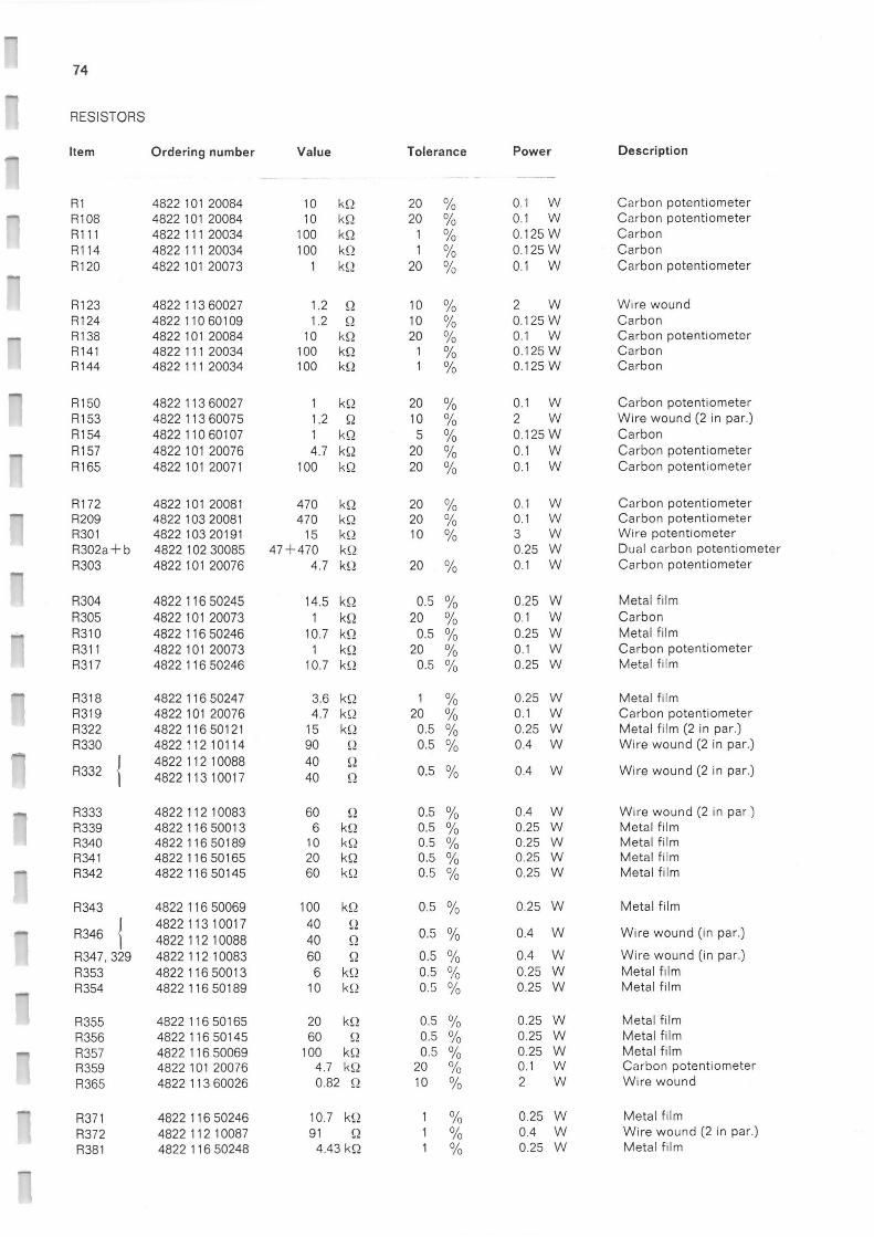
74
RESISTORS
Item Ordering number Value Tolerance Power Description
R1 4822 101 20084 10 kS? 20 0.1 W Carbon potentiometer --~ R 108 4822 101 20084 10 kQ 20 0.1 W Carbon potentiometer
R111 4822 111 20034 100 kS? 1 0.125 W Carbon R114 4822 111 20034 100 k S2 1 0.125 W Carbon R120 4822 101 20073 1 kS? 20 0.1 W Carbon potentiometer
R123 4822 1 13 60027 1.2 2 10 2 W Wire wound R124 4822 1 10 60109 1.2 n 10 0.125 W Carbon
,.._ R 138 4822 101 20084 10 kS? 20 0.1 W Carbon potentiometer R141 4822 111 20034 100 kS2 1 0.125 W Carbon R144 4822 111 20034 100 k52 1 0.125 W Carbon
R150 4822 113 60027 1 kS? 20 0.1 W Carbon potentiometer R153 4822 113 60075 1, 2 52 10 2 W Wire wound (2 in par.) R154 4822 110 60107 1 kn 5 0.125 W Carbon
_ R157 4822 101 20076 4.7 kS2 20 0.1 W Carbon potentiometer R165 4822 101 20071 100 kS2 20 0.1 W Carbon potentiometer
R172 4822 101 20081 470 k52 20 0.1 W Carbon potentiometer R209 4822 103 20081 470 kS2 20 0.1 W Carbon potentiometer R301 4822 103 20191 15 k2 10 3 W Wire potentiometer R 302 a -F b 4822 102 30085 47+470 kS2 0.25 W Dual carbon potentiometer R303 4822 101 20076 4.7 kS2 20 0.1 W Carbon potentiometer
R304 4822 116 50245 14.5 kS? 0.5 0.25 W Metal film 8305 4822 101 20073 1 kS2 20 0.1 W Carbon
.... R310 4822 116 50246 10.7 k4 0.5 0.25 W Metal film R311 4822 101 20073 1 kS? 20 0.1 W Carbon potentiometer R317 4822 1 16 50246 10.7 kS2 0.5 % 0.25 W Metal film
"' R318 4822 116 50247 3.6 k52 1 0.25 W Metal film R319 4822 101 20076 4.7 k52 20 0.1 W Carbon potentiometer R322 4822 i 16 50121 15 k5? 0.5 0.25 W Metal film (2 in par.) R330 4822 ' 12 10114 90 S2 0.5 0.4 W Wire wound (2 in par.)
8332 4822 112 10088 4822 113 10017
40 52 40 52
0.5 0.4 W Wire wound (2 in par.)
..~ R333 4822 112 10083 60 52 0.5 0.4 W Wire wound (2 in par.) 8339 4822 1 16 50013 6 kSZ 0.5 0.25 W Metal film R 340 4822 116 50189 10 k S? 0.5 0.25 W Metal film R341 4822 1 16 50165 20 kS2 0.5 °% 0.25 W Metal film R342 4822 116 50145 60 kSZ 0.5 0.25 W Metal film
R343 4822 116 50069 100 kS2 0.5 0.25 W Metal film 4822 113 10017 40
R346 4822 112 10088 40 n 0.5 0.4 W Wire wound (in par.)
R347, 329 4822 112 10083 60 SZ 0.5 0.4 W Wire wound (in par.) R353 4822 1 16 50013 6 kS2 0.5 0.25 W Metal film R 354 4822 1 16 50189 10 kS? 0.5 0.25 W Metal film
R 355 4822 1 16 50165 20 kS2 0.5 0.25 W Metal film R 356 4822 116 50145 60 S2 0.5 0.25 W Metal film R 357 4822 1 16 50069 100 kS~ 0.5 0.25 W Metal film R359 4822 101 20076 4.7 kS2 20 0.1 W Carbon potentiometer
R365 4822 113 60026 0.82 S? 10 2 W Wire wound
R371 4822 116 50246 10.7 kS? 1 0.25 W Metal film
R372 4822 112 10087 91 S? 1 0.4 W Wire wound (2 in par.) R381 4822 116 50248 4.43 kS? 1 0.25 W Metal film

75
Item
8382 8383 R384 8385
Ordering number
4822 116 50249 4822 116 50037 4822 1 16 50037 4822 1 13 40035
R401a+b 4822 102 30085
R402 4822 103 20186 R403 4822 101 20076 R404 4822 116 50245 R405 4822 101 20073 R407 4822 116 50254
R410 4822 1 16 50246 R417 4822 116 50246 R418 4822 1 16 50024 R419 4822 101 20076 8422 4822 116 50121
R428 4822 116 50037 R429 4822 116 50037 R430 4822 116 50249 R431 4822 116 50029
4822 116 50132 R432 1 4822 116 50099
R433 4822 1 16 5C252 R434 4822 1 16 50253 R435 4822 116 50254 R436 4822 116 50255 R437 4822 116 50145
R438 4822 116 50118 R439 4822 116 50118 R445 4822 112 10081 R501 4822 113 60056 R502 4822 1 13 60056
R503 4822 112 20047 R504 4822 112 20105 R505 4822 112 20045 8506 4822 112 20054 R507 4822 112 20067
R508 4822 1 12 20072 R509 4822 112 20081 8510 4822 112 20094 R511 4822 110 40098 R512 4822 110 40107
R513 4822 110 40121 R514 4822 110 40125 R515 4822 110 40134 R516 4822 110 50147 R517 4822 1 10 50152
R518 4822 110 50161 R519 4822 110 50174 R520 4822 110 50178 R521 4822 1 10 50187 R522 4822 110 50201
Value
2.8 kS2 8.45 kc? 8.45 kS2
333 <_? 47+470 k2
47 kS? 4.7 k~?
14.5 kQ 1 k<_? 1.74 k4
10.7 kS2 10.7 k~?
1.35 k5? 4.7 k52
15 k S?
8.45 k4 8.45 kS2 2.8 kn 1.27 kS2 1.15 kn 1.15 kc?
584 323 103 51 30
10 5 50
1 1
5.6 8.2 4.7 10 33
47 100 330 470
1
kQ k S? k4 kS2 kS?
k5Z k52
S2 n n
;o:o
~~
~
4 S2 n
S2 kS?
3.3 kn 4.7 kn
10 kS? 33 k2 47 kS?
100 kS? 330 kS? 470 kS?
1 M S2 3.3 M S2
Tolerance Power Description
1 0.25 W Metal film 1 0.25 W Metal film 1 0.25 W Metal film 0.5 0.4 W Wire wound
0.25 W Dual carbon potentiometer
3 W Wire potentiometer 20 0.1 W Carbon potentiometer 0.5 0.25 W Metal film 20 0.1 W Carbon potentiometer 0.5 0.25 W Metal film
0.5 0.25 W Metal film 0.5 0.25 W Metal film 0.5 0.25 W Metal film 20 0.1 W Carbon potentiometer 0.5 0.25 W Metal film (2 in par.)
1 0.25 W Metal film 1 0.25 W Metal film 1 0.25 W Metal film 1 0.25 W Metal film (2 in par.)
1 0.25 W Metal film (in par.)
1 0.25 W Metal film 1 0.25 W Metal film 1 0.25 W Metal film 1 0.25 W Metal film 1 0.25 W Metal film (2 in par.)
1 0.25 W Metal film 1 0.25 W Metal film (2 in par.) 0.5 0.4 W Wire wound (2 in par.) 10 2 W Wire wound 10 2 W Wire wound
10 5.5 W Wire wound 10 5.5 W Wire wound 10 5.5 W Wire wound 10 5.5 W Wire wound 10 % 5.5 W Wire wound
10 5.5 W Wire wound 10 5.5 W Wire wound 5 5.5 W Wire wound 5 0.5 W Carbon 5 0.5 W Carbon
5 0.5 W Carbon 5 0.5 W Carbon 5 0.25 W Carbon 5 % 0.25 W Carbon 5 0.25 W Carbon
5 0.25 W Carbon 5 0.25 W Carbon 5 0.25 W Carbon 5 0.25 W Carbon 10 0.25 W Carbon

76
Item Ordering number Value Tolerance Power Description
R523 4822 110 50205 4.7 MS2 10 % 0.25 W Carbon R601 4822 115 80075 Shunt R602 4822 1 15 80077 Shunt
_. R603 4822 1 15 80078 Shunt 8604 4822 115 80078 Shunt
R605 4822 115 80079 Shunt - R606 4822 115 80079 Shunt
R607 4822 116 50144 50 k~2 0.5 % 0.25 W Metal film R608 4822 116 50145 30 kS2 0.5 % 0.25 W Metal film (2 in par.) R609 4822 116 50118 10 kS2 0.5 % 0.25 W Metal film
8610 4822 1 16 50118 5 k5? 0.5 % 0.25 W Metal film (2 in par.) R611 4822 112 10119 3 kS2 0.5 % 0.4 W Wire wound
- 8619 4822 112 10054 5 5? 0.5 % 0.4 W Wire wound (2 in par.) R622 4822 115 80081 Shunt R623 4822 115 80081 Shunt
- R631 4822 110 30134 10 kS? 1 % 0.125 W Carbon R708 4822 113 10001 1.54 kS2 1 % 0.4 W Wire wound R728 4822 113 10001 1.54 kS? 1 % 0.4 W Wire wound R802 4822 101 20071 100 kc_? 20 % 0.1 W Carbon potentiometer
-~ R806 4822 101 20076 4.7 kS2 20 % 0.1 W Carbon potentiometer
R811 482210120073 1 k5? 20 0.1 W Carbon potentiometer R833 4822101 20084 10 kS2 20 0.1 W Carbon potentiometer - R841 4822 116 30062 15 kS? 20 0.6 W N.T.C. R901 4822101 50059 47 kS? 20 0.125 W Carbon potentiometer 8902 4822 102 30136 2x22 kS2 Dual potentiometer
R903 4822 103 20081 22 k~? 20 % 0.1 W Carbon potentiometer R905 4822 101 20084 10 kS2 20 % 0.1 W Carbon potentiometer R962 4822 116 50366 151.5 k5? 0.25 % 0.25 W Metal film
- R966 4822 116 50367 85.9 kS? 0.25 % 0.25 W Metal film R970 4822 116 50368 59.9 k52 0.25 % 0.25 W Metal film
R974 4822 116 50369 46 k52 0.25 % 0.25 W Metal film '-" R978 4822 116 50371 37.25 kS? 0.25 % 0.25 W Metal film
R982 4822 116 50372 31.24 kn 0.25 % 0.25 W Metal film R986 4822 116 50373 26.83 k2 0.25 % 0.25 W Metal film R1001 4822 113 80027 47 kS? 5 % 16 W Wire wound
R1002 4822 113 80015 33 kn 5 % 16 W Wire wound R1003 4822 11540109 10 k52 5 % 16 W Wire wound
-- R1004 4822 115 40095 4.7 k2 5 % 16 W Wire wound R1005 4822 115 50102 3.3 kS2 5 % 40 W Wire wound R1006 4822 115 50073 1 k~? 5 % 40 W Wire wound
"' R1007 4822 115 50069 470 S? 5 % 40 W Wire wound R 1008 4822 115 50067 330 n 5 % 40 W Wire wou n d R1009 4822 115 50062 100 S? 5 % 40 W Wire wound
(adjusted to 100 S?) - R1010 4822 115 50061 47 <.2 5 % 40 W Wire wound
(adjusted to 47 S2) R1011 4822 11550059 33 S2 5 % 40 W Wire wound
_ (adjusted to 33 ~?) R1012 482211550055 10 2 5 % 40 W Wire wound R1013 482211550119 4.7 S2 5 % 40 W Wire wound R1014 4822 115 50002 3.3 ~? 10 % 25 W Wire wound
_.. R1303 4822 101 20084 10 k2 20 % 0.1 W Carbon potentiometer R1304 4822 101 20084 10 kS2 20 % 0.1 W Carbon potentiometer

77
MISCELLANEOUS
Item Ordering number
T1 2422 530 01407
T2 T3 T4 T201
T1101 L1 L601 L1201 L1202
L1203 L1204 LA1 LA2 LA3 B1
4822 146 40163 4822 148 20075 4822 148 20075 4822 158 40034
4822 148 20076 4822 150 10072 4822 158 10132 4822 526 10036 4822 526 10036
4822 526 10036 4822 526 10036 4822 134 40054 4822 134 40005 4822 134 40005 AW 17/69
6 V, 0.1 A 6.3 V, 0.63 W 6.3 V, 0.63 W
Complete printed-wiring boards U 1 4822 216 90074 U 1 A 4822 216 90234 U2 4822 216 90075 U3A 4822 216 90076 U36 4822 216 90177
U3C U4A U46 U4C U5A
U6A U7 U8A U9A U9B
U11A U13 RE801 VL1 VL2 VL3
4822 216 90078 4822 216 90176 4822 216 90079 4822 216 90081 4822 216 90082
4822 216 90083 4822 216 90084 4822 216 90178 4822 216 90086 4822 216 90087
4822 216 90088 4822 216 90089 4822 280 70032 4822 253 30025 4822 253 30025 4822 252 20001
2A, delayed action 2A, delayed action 125° C
Description
Variable transformer (supplied by ELCOMA) Mains transformer Collector transformer Collector transformer H.T. transformer
H.T. transformer Deflection coil Wide-band choke Wide-band choke Wide-band choke
Wide-band choke Wide-band choke Bulb Bulb Bulb C.R.T.
Final amplifier (tensity control H.T. circuit Pre-amplifier X-deflection coefficients
X-deflection coefficients Pre-amplifier Y-deflection soefficients Y-deflection soefficients Base resistors
Shunt plate Power supply Final amplifier Step generator Ring counter
H.T. circuit Adjusting circuit Relay Fuse Fuse Fuse
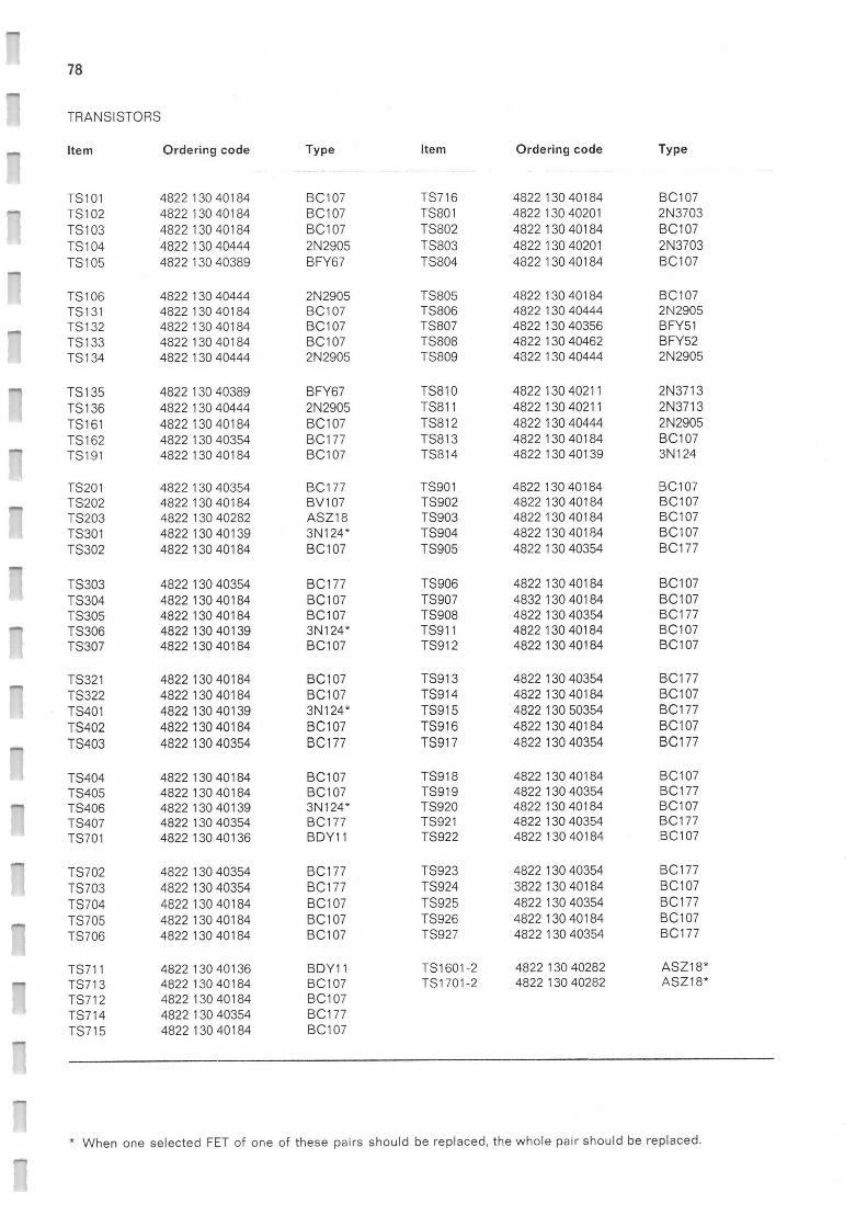
78
TRANSISTORS
,..., Item Ordering code Type Item Ordering code Type
TS101 4822 130 40184 BC107 TS716 4822 130 40184 BC107 —` TS102 482213040184 BC107 TS801 482213040201 2N3703
TS103 4822 130 40184 BC107 TS802 4822 130 40184 BC107 TS 104 4822 130 40444 2N2905 TS803 4822 130 40201 2N3703 TS105 4822 130 40389 BFY67 TS804 4822 130 40184 BC107
TS106 482213040444 2N2905 TS805 482213040184 BC107 TS131 4822 130 40184 BC107 TS806 4822 130 40444 2N2905
,r , TS132 4822 130 40184 BC107 TS807 4822 130 40356 BFY51 TS133 4822 130 40184 BC107 TS808 4822 130 40462 BFY52 TS134 4822 130 40444 2N2905 TS809 4822 130 40444 2N2905
—' TS135 4822 130 40389 BFY67 TS810 4822 130 40211 2N3713 TS136 4822 130 40444 2N2905 TS811 4822 130 40211 2N3713 TS161 4822 130 40184 BC107 TS812 4822 130 40444 2N2905 TS162 4822 130 40354 BC177 TS813 4822 130 40184 BC107
"~ TS191 482213040184 BC107 TS814 482213040139 3N124
TS201 482213040354 BC177 TS901 482213040184 BC107
._ TS202 4822 130 40184 BV107 TS902 4822 130 40184 BC107 TS203 4822 130 40282 ASZ18 TS903 4822 130 40184 BC107 TS301 4822 130 40139 3N124* TS904 4822 130 40184 BC107 TS302 4822 130 40184 BC107 TS905 4822 130 40354 BC177
TS303 4822 130 40354 BC177 TS906 4822 130 40184 BC107 TS304 4822 130 40184 BC107 TS907 4832 130 40184 BC107 TS305 4822 130 40184 BC107 TS908 4822 130 40354 BC177
"` TS306 4822 130 40139 3N124* TS911 4822 130 40184 BC107 TS307 4822 130 40184 BC107 TS912 4822 130 40184 BC107
TS321 4822 130 40184 BC107 TS913 4822 130 40354 BC177 TS322 4822 130 40184 BC107 TS914 4822 130 40184 BC107 TS401 4822 130 40139 3N124* TS915 4822 130 50354 BC177 TS402 4822 130 40184 BC107 TS916 4822 130 40184 BC107
..., TS403 4822 130 40354 BC177 TS917 4822 130 40354 BC177
TS404 4822 130 40184 BC107 TS918 4822 130 40184 BC107 TS405 4822 130 40184 BC107 TS919 4822 130 40354 BC177
"' TS406 482213040139 3N124* TS920 482213040184 BC107 TS407 4822 130 40354 BC177 TS921 4822 130 40354 BC177
TS701 4822 130 40136 BDY11 TS922 4822 130 40184 BC107
TS702 4822 130 40354 BC177 TS923 4822 130 40354 BC177
TS703 4822 130 40354 BC177 TS924 3822 130 40184 BC107 TS704 4822 130 40184 BC107 TS925 4822 130 40354 BC177
.., TS705 4822 130 40184 BC107 TS926 4822 130 40184 BC107 TS706 4822 130 40184 BC107 TS927 4822 130 40354 BC177
TS711 4822 130 40136 BDY11 TS1601-2 4822 130 40282 ASZ18* —~ TS713 4822 130 40184 BC107 TS1701-2 4822 130 40282 ASZ18*
TS712 482213040184 BC107 TS714 4822 130 40354 BC177 TS715 4822 130 40184 BC107
* When one selected FET of one of these pairs should be replaced, the whole pair should be replaced.

79
DIODES
Item Ordering code Type Item Ordering code Type
GR1 4822 130 30198 KBS01(2) GR712 4822 130 30273 BAX16
GR92 4822 130 30281 OA91 GR713 4822 130 30273 BAX16 _ GR93 4822 130 30245 BZY63 GR714 4822 130 30193 BZY88/C5V6
GR101 4822 130 30273 BAX16* GR716 4822 130 30195 BYX10
GR102 4822 130 30273 BAX16* GR721 4822 130 30273 BAX 16
GR103 4822 130 30229 AAZ15 GR722 4822 130 30193 BZY88i C5V6
GR104 4822 130 30273 BAX16 GR724 4822 130 30195 BYX10
G R 105 4822 130 30084 AAZ 18 GR801 4822 130 30273 BAX16
"— GR106 4822 130 30084 AAZ18 GR802 4822 130 30273 BAX16
GR131 4822 130 30273 BAX16* G R803 4822 130 30196 BZY60
_ GR132 4822 130 30273 BAX16* G R804 4822 130 30273 BAX 16 GR133 4822 130 30229 AAZ15 GR805 4822 130 30273 BAX16 GR134 4822 130 30273 BAX16 G R901 4822 1 30 30273 BAX16 GR135 4822 130 30084 AAZ18 GR902 4822 130 30273 BAX16
—^ GR136 4822 130 30084 AAZ18 G R903 4822 130 30273 BAX16
GR201 4822 130 30195 BYX10 G 8904 4822 130 30273 BAX 16
GR202 4822 130 30195 BYX10 G R905 4822 130 30273 BAX 16
GR203 4822 130 30296 BY140 GR906 4822 130 30273 BAX16 GR205 4822 130 30296 BY140 GR907 4822 130 30273 BAX16 GR301 4822 130 30303 BAY32 GR908 4822 130 30273 BAX16
GR302 4822 130 30303 BAY32 GR909 4822 130 30191 OA95 GR303 4822 130 301.89 BA114 G R910 4822 130 30273 BAX16 GR304 4822 130 30132 BZY59 GR911 4822 130 30273 BAX16
—' GR305 4822 130 30132 BZY59 GR912 4822 130 30273 BAX16
GR306 4822 130 30189 BA114 GR913 4822 130 30273 BAX16
GR307 4822 130 30303 BAY32 GR914 4822 130 30273 BAX16 GR308 4822 130 30303 BAY32 GR915 4822 130 30273 BAX16 GR309 4822 130 30189 BA114 GR916 4822 130 30191 OA95 GR310 4822 130 30189 BA1 14 GR917 4822 130 30191 O A95
^ GR311 4822 130 30132 BZY59 GR918 4822 130 30191 OA95
GR401 4822 130 30303 BAY32 GR919 4822 130 30191 OA95 GR402 4822 130 30303 BAY32 GR920 4822 130 30191 OA95 GR403 4822 130 30189 BA114 GR923 . 40 4822130 30191 OA95 GR404 4822 130 30132 BZY59 GR1101 4822 130 30296 BY140
GR405 4822 130 30132 BZY59 GR1301 4822 130 30273 BAX16
GR406 4822 130 30189 BA1 14 GR1501 4822 130 30195 BYX10 GR407 4822 130 30303 ZAY32 G R 1502 4822 130 30195 BYX10 GR408 4822 130 30303 BAY32 G R 1503 4822 7 30 30277 BYX28/400R
-~ GR409 4822 130 30189 BA1 14 G R 1504 4822 130 30277 BYX28/ 400R GR410 4822 130 30189 BA114
GR421 4822 130 30276 BYX20/200R _ GR422 4822 130 30276 BYX20/200 GR701 4822 130 30198 KBS01(2) GR702 4822 130 30279 BY123 GR711 4822 130 30273 BAX16
* These components are selected. Phase refer to the selecting procedure at the end of this chapter.
80
Selection procedures for semi-conductors
—When replacing the power transistors TS1601, 1602, ,^ 1701 and 1702, the replacements should be selected
for a leakage current ~ 10 mA at a V, i.;it-voltage of 50 V.
30V
—When replacing the diodes GR101, 102, 131 and 132, the replacements should be selected for a voltage Ua (see diagram) between 490 and 520 mV, which corresponds to an indication of 90 to 120 mV on the voltmeter.
DIGITAL VOLTMETER
BAX 16
81
R2 100M
R1
C3 ~ SK 2 R 3 ~~220~
~ooK C4 C" SK1
~—o--
LOOM
C1 ~~'
C2
—I izzo~S ~ 2 Diode under test
KN----O j CS 1
~/ ZT: ~~
J PM 6546
Fig. 87. Diagram PM 6546
PEM4516
Fig. 88. Printed wiring board PM 6546
82
SK2/I
SK2/II
Fig. 89. Switch wafers SK2
23 22 ~O, 3
?t fie_ 1 : 4 20 ~~ S
g ,~ G
18 O
~ ~ ~ ~ g
~ ~ 9 ~ •~ t0
d 11 ij 12
SK12/I
SK12/II
SK1O/I
SK1O/II
22 "b
Q~ 3
20
~ •~
5
6 13 H
6
7 8 ~ 0 1
8 t7 ~ ~ 8
10 1; • +o
SK1O/III
SK1O/IV
2d 1 ~ C1 5
21 ~~~~
4 21 ~ ~
q5 ~ 5 Yo
l9 G m ~ ~~ G
t4 ~~ 0 ~ 9 ~ O
~ ~
~ ~ ~Q~~ w A to ~~ 9
1
Fig. 90. Switch wafers SK1O
15
?t L i% 4 21 20 h 20
g 6 B
~ ~ 7 8
>7 ~— v e 17 16 g 16
15 • 10 'd ,, ro 11
SK13/I
SK13/II
~ ~ Q 3 ~ Qi 3 21 ~~ ~ q 21 L ~ ~ q
to ~ >~ 5 E~ J7 ~ 5
O
0~ G
~~' '~ ~ ~~ ~~ e~ e e ~ e
7L ~ ~ 9 t j 9
SK13/111
SK13/IV
21 ~~ 4
40 ~_~ ~ 5
B ~ / O~i 6
fe N ~~ ql+~ +~ ~~~—% e G~~ 9
Is • w I5 • a 15
Fig. 91. Switch wafers SK12 Fig. 92. Switch wafers SK13

83
SK16/I
SK16/II
Fig. 93. Switch wafers SK16
T2
t ~ ~ I I i u . I I I
n ,
t ;~ ~ ~~..~• r: .• •... ~ u--
sron u~~
SK16/III
SK16/IV
23 2d 1
2 ?2
0 3
1t i i J 4
20 ~ y"'~C ~~ 5 19 ~'
0
G
g~ w~ 8 t~ ,~~ s
9 16 ~ ~ 9 tp 15 t0
I4 11
SK16/V
SK16/VI
43 p S 2! 0 3 • !1 4
5 20 ~ 'r~ 5
G 19 H
O ~ 6
7 t8 7
9 ~ ;. 9 i5 ~ ro
N
T3-T4
Fig. 94. Connection diagram for mains transformer T2 Fig. 95. Connection diagram for collector transformers T3 and T4
T201
n
T 1101
II I I II
~~ ~ ( ~?
~ I ~ II i~ i I ~i
- I~ ~I~ ~-.,
~ ~~~ 1 5
Fig. 96. Connection diagram for H.T. transformer T201 Fig. 97. Connection diagram for H.T. transformer T1101

84
24
25f 2s f•
n W
O GR13t
RTTI
27 ~
2e t
29~
301
31~
1
w a T
R'33
rc 3#
R 135
R39 E- '
R4(
~~~
R66
R10
R62 • R43
GR61~ --~ ` R45 }-
GR ~ ~R74~- E
R146
GR134
-{ R 153
-{ R 14 9 1--
O «-{ R 9 }-- ~ .
a --~ R 15 S \
T -~ RI3 }-- E f
-{ R5 -
R3 }-" I
32
33a~
33 C O~
e
0
R76 w~
w
T
a
w®S
G161 +
i
^ R63
u 9 t0 1Da 11 12 13 R17
~ v
35~ n ~~
36~ 0
371 ~~—
^L, 1
m
\~
G
p
~;
I
x
+~ m A
- e o 0 ll
48
~23g
'L2u
/~
19p ~~ U
15~
14~
. nE
t u5
w
n
u
u
3
PEM3866A
Fig. 98. Printed wiring board U1, final amplifier, and U1A intensity control

85
~
/
0
Fig. 99. Printed wiring board U2, H. I . circuit
86
C3
o 3N
m ~
t° a
-`GR9 he `0 ~{ R 15 ~- r ,,~~4;
CI K, ~R7 ~ ~ 1, _
K GRt r ~'t'561 ~ ~'
s--{ R 70 -- -MGR 8?~ ~ ~GRR2r.KF
-{R24~ ~ -[R25r
+~3~.5,a r}
~a~ 5 o B a 7
--~~,y_ 12
~_.1 ~~ ~ ao
`-r'
PEM 3875
0
R II
Fig. 100. Printed wiring board U3A, pre-amplifier

87
.---~ /
~ \ - IIII
0
PEM 3883
Fig. 101. Printed wiring board U3B, X-deflection

88
PEM 3877
Fig. 102. Printed wiring board U3C, X-deflection

89
~ ~
l ~
d
a ~•
•~• •~•
-~
t ) ■
PEM 3876
Fig. 103. Printed wiring board U4A, pre-amplifier

90
~`
~`
•• •~• ~~•
PEM 48 73
Fig. 104. Printed wiring board U4B, Y-deflection

91
~-
1
O t ? 3 4 5 6 1 8 9
PEM 3881
Fig. 105. Printed wiring board U4C. Y-deflection
••• .•. •.•
PEM 3882

92
1 ~~ L
PEM 3 869
Fig. 706. Printed wiring board U5A, base resistors

93
s ~soi
~D
N t0
O M c0 O
cD O
+£N
iFf Q N tD
O
0 t4
fY
O t9
N
PEM 3870
Fig. 107. Printed wiring board U6A, shunt plate

94
•~ 17 T6 l5 14 i3 12
~ • • • -tcnnz?`
N
G7
7
h r I } N~ ~'m~ ~ 9
fist ~ 10
}.~ `~ o„
PEM 3865 Q
Fig. 108. Printed wiring board U17, power supply

95
PAM ae~s
Fig. 109. Printed wiring board U8A, final amplifier

96
~ C9Q1
C902
0904
—{ R506}-
11 r— m m m ~ ~ TT
9 7 6 5 .., .. ~ (l .: w r
—{ R914
'~ -{~~¢ ~^ -~~- —~ R 919 (-=-
» i -~.818~4 -(Cr~i l l ~ r Z-(GR l~ - Q
PEM3872
Fig. t 10. Printed wiring board U9A, step generator

97
11 1e s e ~ c s ~ 3 z 1
~®
1 R956}-25
^-~.
"{
II..~R.~G~ 7 S Q
(~~ -{ R958 +- ti~ g~ -{ R957 f -
© E1
I C 922 I -~ R 959}-
R96
R2
~ 13
T ..14i
~~~j
~~~:
~" 14 c~z~
X15
(1
[~Y~~
15 fi
~~
19
c~z:,
-~R963}~
~+~ g 'LJ" E
{ R 966 {-iR967f-
~% 19 E ZY=Yr✓
-~ R 970 ~-
R97 f~^
(r~ -~ R974
X16 [~Y~~ -~ R977 ~--~Rs7s ~-GR
35
X17 G 927 R 97 9
_/ E i
~ ~'
X18 ~. '~
\~JE~
~{ R985~ ~~
\G:~~ '~ -~ R 986
~-
PEM 3871
Fig. 111. Printed wiring board U9B, ring-counter

98
0
0
~/
PEM3878
Fig. 112. Printed wiring board U11A, high-tension unit

99
/~
PEM 3874
Fig. 113. Printed-wiring board U13, adjusting circuit
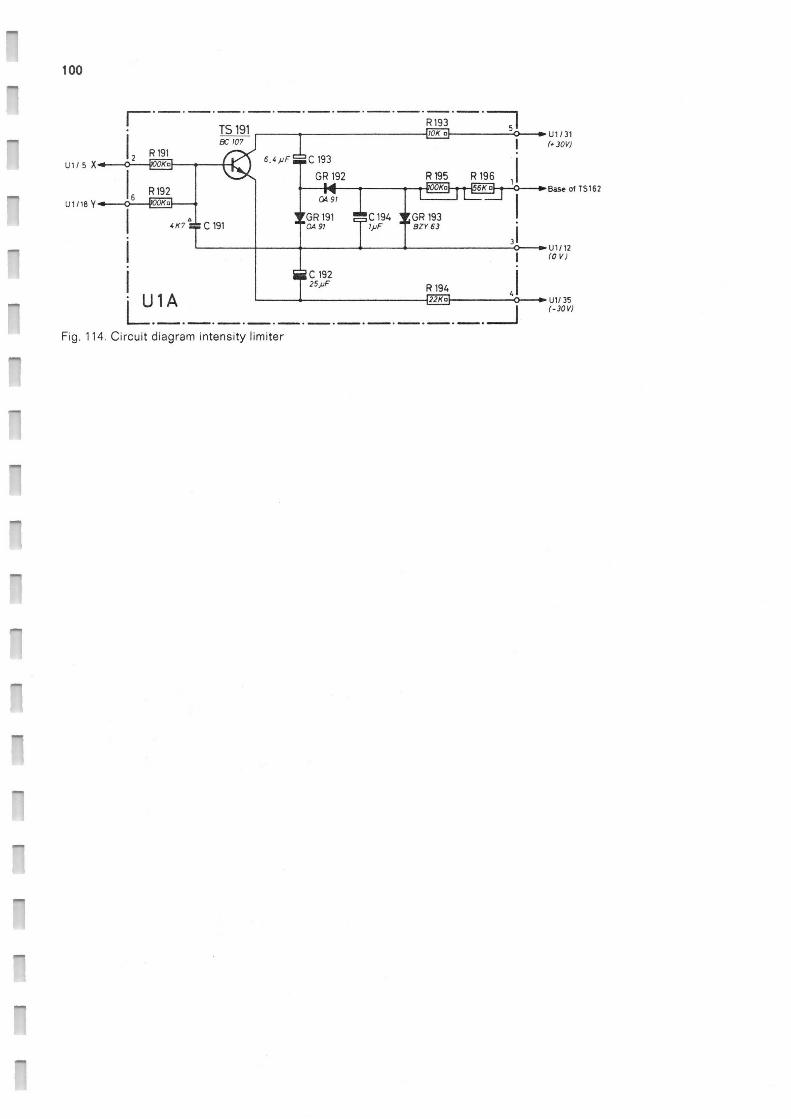
100
12 R 191 U 1 / 5 X OKo
R 192 u 1 / 1e Y ~--~(r00Ko~.--~
I <K~°~C,9,
T5191BC 109
6,<wF ~C 193
GR 192
R 193 'lOK o1
R 195
04 97
=GR 191 oC 194 Q4 91 1vF
GR 193 BZY 63
R196 1I
Fig. 114. Circuit diagram intensity limiter
o C 192 T 25NF R 194 12Ko
.~
U1/31 (• 30VJ
ase o1T5162
U1/ 12 (0 VJ
U1/ 35 (-30V1

i Pf}MER OM
rSj l ~ SK21 VLt o
v °I -~~
L2 `
L.g~ L ~! 14
I
SK 23
T2
G
Iz 6s
z
~ tSV -t p"J
~ \~iBV OY `I~ ~~ 17 .l
GS$V
GRI{ gAX'6
TS @41
~~ 3V —_J
s ~i4Y+
~ti, ~cla ~a2LUF
GR2
)~ 8Y 17) ,y
\ ~~/ --Y
i~ R3< "F, si r i
• ~ Jf
C25
1
GRAS EYk 70
ec qr
I s,uF ~28 GR2i
R21 trAxra~ j y
~R2ti ! ~0,6Va i R_23 rRr ~
♦38V 18Y 1 ~ ~_.. _.__.__
-i6V i OV s 8V i
~_G~R~I2~ GR13
BAX1a►f g(X!6
1 R4 ~Ci3
QyF
~~ aT
R
TS14 B: !OT
~TS12 j 1. . 10TrpT
--;
LA1 ~~~ LA2 LA3
~,~- ~~,r - ~ ~~ .d~~ e-1L. goo l'Res+o tsrn _-s wo ~o 0
_ 11
R29" R33
C7~ ~!Ri2 ~:YT ~
R 3!f
~~ II
C141 ►1,C15 IrsaK ~irx R37
~ I~gii
~ ~ 11 GRt7 ~
QApS 1 1':495
~ if 4„v~R30
I 1
L
„R9 GRi
CS 1 e~a
~~ ~
8G 1414
~la R 38~Yi
{{
(h
K8
1~ i; I;r
l: ::rCLE
~ 1
R f3
I
zsuv
C24r~
~~~'~
~R2B BGRZ 2
ez~ae~ s ve -30 V
e u
OY 5-T
~31,+~V
I
r :iGSi
GRI6 evxro
GR29
avx p
3+.
U7
'' {~ CURVESJSEC. 1 V ~,> p a—~ 1111111 100 F ROM 0
!"'~i / ' '~ 1 2oa
SK 1 •OG ?U 0
11
- *3t,5V
~-~ I r.~_ _.lR90 ~ R504
aa0
~ ` y Cl19 ~1~ .
~~R9~ ~ 1,zv
R 24
R22 GRt2
ewx ra aAx:~s
r'" ~~~
A R4C1 1 8 R47
a ~ R991{~ S~tgg]
L .~.~ ..~
+ISY I
SK19/A Y'K!9/C SK 14l8 y~ g
L.. ~~~~"~,--
~30~
G
jY
sWltcliwFGslrlon too~.~ ~~^ SK 12 ! t,/
~ ~
r~ i+A 7~ 22 !S¢ ~
7 R1 T~Y_,~,v_~$19_I~ i ~
iJ
R
ROI R!2
+ R71 C2S ~. : w
:~5
-45V t-eG v;
r —•- -.~~
SK9!6 ~a---t
GRI
I
1 ~ ~~
GRp ~ ~ SKl9/$ BYxq 1
1 ~•
~iRt ..~ ~ LJ
RE40
BY Ip
s~~a
' ~0V
1 2
2e
R~ I
Ax!a
ecroT 1070 ~C12
23V
7501( }OwF
r1LCtt xs
+30V ~•'=
Ct3 ~r
Ix5
r
c' ~ ~~ ~
R15
RI
-30V
~—
R
3av
1
\^ rh. T57 <
+3ov IY
_,
~+- e6 yYM
C4
WS
TSB.
:ate 3 ~' ~.
BAx,a ~~R26
rs V
R 39
R iL0
,~
'P T
GR29
ass
TS
GR 31
ass
R64 ~RtiB
tt ~y
SK 1 0/~_ "~ SKK?/M
.~
W17CN IN FULLY COUNTER -CLOCK WISE• POSIr ICN •_~•~ ~
i
SKl3J1
O ~ U
p~ U
SK 3 STEF,~FAM.
1 SK t ~ 'p'""~
SpUpr F ~ -)ISi4kCc I i R 1
zl r '
,R2...22
9 ,aQ-"~, ~~IR2)
~ ti' r ~_~ ~r ~
j nU5
R1203 ,~R~w
R4NGKfWi INPil
*SK t1
j+30V
R`_~~ 1bSK20os RG~
Ii
RI
f
q O—
SKlB 1
Kt9/C
1 ~ 5K I$.'C
SK19/C
,Y~o1..t r
O~
-3Gv
SKt3JII y
SK f6/~
+ SK16/j ,.
U4B~J
gas I4~RB6
U9B
1A
Irzo= t+2o:i
BU2/A
BU 3/$
~8
:12~/R
+O'
i °J i ~3~
~t---
Rno!
+30V
GRI
t
R7s t! 3821 BAY):
GR7f ~;R71 Bzrss
~~
,YI ~ R 73 ~~I,R72
_~ en
~ 1
-30V
+ 30Y
GRt eAru
1'SV1 R29
Res --~---f`=SI1
i
+ 30 V~2
0
Ci
J?MT
~3G% L r
GP.2• BAYla 1
GR 3 au ru
R4 =
•R~
~~'2
lam ^ Y,} Xi KS ib ~ SK 17 0 ~.~ ~ 5 J
"`..'_
_rz~ II!
Rib Ip
T5 7
+ 30V
r R23~ i G` x I 4 X SM61
' ~ ~R20 ~ R302 I
u3A ~ u~ ~
i
R12 t'R15 ~R2G
TS i BcroT
P r R3~i
R
R6
-~'~- 1 V
?3V TS2
FL q
~~E M5
~~
GR9
~ K
TS7 BC gTgT
a
Ts/b r n 5 Y
C4 GRt
~ ~ ~~ ~~
~GR2 erxq
tl
t
vR3 Brrp
C5 GR5 -;t
a~ c
} 30V
R40 __ _~
)S
+3ov_„
U4A __.1 U4
C7 ~iY
iR$
;S'J
IR 10
R 32 I BA x!a C3i i
ss
s ❑
a 4 w'4
~w ,_~~; °fs~~1
,r ,~ ~• ~ ~ . e ~11` ~ `s
*GR32 six u
R37
R 92 Q~l.',
TS?~5 hviLYtS
,~
zo
~zx.2~
LU17
"-'-18Y
u~
,e~
J
PEM 3fi36A
Fig. ~ 15. Circui± ci~c~ram PM 657

Sales and service all over the world
Algerie: S.A. Philips Nord-Africaine, Route de la Femme Sauvage, Alger; tel. 647 200/1/2
Argentina: Philips Argentina S.A., Casilla Correo 3479, Buenos Aires; tel. T.E. 70, 7741 al 7749
Australia: Philips Electrical (Pty) Ltd., P.O.B. 2703 G.P.O., 69-79 Clarence Street, Sydney; tel. 20-223
Belgie/Belgique: M.B.L. E., 80 Rue des Deux Gares, Bruxelles; tel. 23 00 00
Bolilvia: Philips Sudamericana, Casilla 1609, La Paz; tel. 5270-5664
Brasil: Messrs. Inbelsa, Rua Amador Bueno 474, Caixa Postal 3159; Sao Paulo; tel. 93-9191
Burma: U Thoung Tin, 36, Barr Street, Rangoon Burundi: Philips S.A.R.L., Avenue de Grece, B.P. 900,
Bujumbura Canada: Phililps Electronic Industries, Electronic Equip-
ment Division, 116 Vanderhoof Avenue, Toronto 17, Ontario; tel. 425-5161
Chile: Philips Chilena S.A., Casilla 2687, Santiago de Chile; tel. 35081
Colombia: Philips Colombiana S.A., Communications Department, Apartado Nacional 1505, Bogota; tel. 473-640
Congo: Philips S.A.R. L., 620, Avenue Industrielle, B.P. 2546, Lubumbashi; Philips Congo S.C.R.L., 137, Bou-levard du 30 Juin, B.P. 1798, Kinshasa; 52, Avenue des Eucalyptus, B.P. 2020, Stanleyville
Costa Rica: Philips le Costa Rica Ltd., Apartado Pos-tal 4325, San Jose; tel. 5670
Curacao: Philips Antillana N.V., Postbus 523, Willem-stad; tel. Curacao 36222-35464
Danmark: Philips A.S., Prags Boulevard 80, Kmben-havn; tel. Asta 2222
Deutschland (Bundesrepublik): Philips Industrie Elek-tronik GmbH., Rdntgenstrasse 22, Postfach 111, 2 Hamburg 63; tel. 501031
Ecuador: Philips Ecuador S.A., Casilla 343, Quito; tel. 30064
EI Salvador: Philips de EI Salvador, Apartado Postal 865, San Salvador; tel. 7441
Egypt: Resident delegate office, P.O.B. 1687, 43 Kasr EI Nil Street, Cairo; tel. 74933
Espana: Philips Iberica S.A.E., Avenida de America, Apartado 2065, Madrid; tel. 2462200
Ethiopia: Philips Ethiopia Priv. Ltd., Co., P.O.B. 659, Cunningham Street, Addis Abeba; tel. 13440
France: Philips Industrie S.A., 105 Rue de Paris, Bo-bigny 93; tel. 845 28-55, 845 27-09
Ghana: Philips (Ghana) Ltd., P.O. Box M 14, Accra

Great Britain: M.E.L. Equipment Company Ltd., Manor _, Royal, Crawley (Sussex}; tel. 28787
Guatemala: Philips de Guatemala S.A., Apartado Pos-tal 238, Guatemala City; tel. 20607-08-09
Hellas: Philips S.A. Hellenique, B.P. 153, Athenes; tel. ._, 230476
Hong Kong: Philips Hong Kong Ltd., P.O.B. 2108, Rooms 1006/1008 Prince's Building. Hong Kong; tel. 33728, 28548
India: Philips India Ltd., PIT/S.E. Dept., 254, Dr. Annie Besant Road, P.O.B. 6598, Worli, Bombay 18; tel. 245144
Iran: Philips Iran Ltd., P.O.B. 1297, Teheran; tel. 48344-"' 68344
Iraq: Philips (Iraq) W.L.L., P.O.B. 5749, South Gate Post Office, Baghdad; tel. 98844
Ireland: Philips Electrical (Ireland) Ltd., Newstead, ~"' Clonskeagh, Dublin 14; tel. 976611
Island: Mr. Snorri P.B. Arnar, P.O.B. 354, Reykjavik; tel. 13869
~., islands Canarias: Philips Iberica S.A.E., Triana 132, Las Palmas 39-41 Santa Cruz de Tenerife
Israel: Isralectra Ltd., 12, Allenby Road, P.O.B. 1608, Haifa; tel. 526231
_ Italia: Philips S.p.A., Casella Postale 3992, Milano; tel. 69.94
Liban: Philips Liban S.A., P.O.B. 670, Beyrouth; tel. 232303-232458/59
-- Malaya: Philips Singapore Ltd., P.O.B. 1358 N.T.S. Building, d'Almeida Street, Singapore; tel. 94914
Maroc: Societe Anonyme Marocaine de Telecommuni-cations, Place Lemaigre Dubreuil, Casablanca; tel.
-- 439-92 Mexico: Philips S.E.T., Apartado Postal 24420, Mexico
7 D.F.; tel. 25-15-40 Nederland: Phililps Bedrijfsapparatuur Nederland N.V.,
` Boschdijk VB, Eindhoven; tel. 3-33-33 Ned. Antillen: Philips Antillana N.V., Postbus 523,
Willemstad, Curagao New Zealand: Electronic Development and Applica-
r tions Co. Ltd., 18-20 Lorne Street, P.O.B. 2097, Wellington; tel. 54-039
Nigeria: Philips (Nigeria) Ltd., Philips House, 6, Ijora ,_ Causeway, P.O.B. 1921, Lagos; tel. 56051/2
Nippon: Philips Products Sales Corporation of Japan, Kokusai Building, 7th Floor, Marunouchi, Chiyoda-Ku, Tokyo; tel. (216)2441
_. Norge: Norsk A.S. Philips, Postboks 5040, Oslo; tel. 463890
Clsterreich: Philips GmbH, Abt. Industrie, Triester-strasse 64, 1101 Wien X; tel. 64 55 11
Pakistan: Philips Electrical Co. of Pakistan Ltd., Bunder Road, P.B. 7101, Karachi; tel. 70071
Paraguay: Phililps del Paraguay S.A., Casilla de Correo 605, Asuncion; tel. 8045-5536-6666
Peru: Philips Peruana S.A., Apartado Postal 1841, Lima; tel. 34620-40265
Philippines: Electronic Development & Application Center, Room 715, Don Santiago Bld., 1344 Taft Ave-nue, Manila
Portugal: Philips Portuguesa S.A.R.L., Rua Joaquim Antonio d'Aquiar 66, Lisboa; tel. 683121 /9
Rhodesia: Philips Rhodesian (Private) Ltd., P.O.B. 994, Gordon Avenue, Salisbury; tel. 29081
Rwanda: Philips Rwanda S.A.R.L., B.P. 449, Kigali Schweiz-Suisse-Svizzera: Philips A.G., Binzstrasse 18,
8027 Zurich 3; tel. 051 44 22 11 Singapore: Philips Singapore Ltd., P.O.B. 1358, N.T.S.
Building, d'Almeida Street, Singapore 1 South Africa: South African Philips (Pty) Ltd., P.O.B.
7703, 2, Herb Street, New Doornfontein, Johannes-burg; tel. 24-0531
Suomi: Oy Phililps Ab, Frederikinkatu 48, Helsinki; tel. 10915
Sudan: Gellatly Hankey & Co. (Engineering) Ltd., P.O.B. 150, Khartoum; tel. 71183
Sverige: Svenska A.B. Philips, Fack, Lidingovagen 50, Stockholm 27; te1. 08/635000
Syrie: Philips Moyen Orient S.A., P.O.B. 2442, Damas; to I. 18605-21650
Taiwan: Yung Kang Trading Co. Ltd., 6 Nan King East Road, 1 Section, P.O.B. 1467, Taipei; tel. 43540
Thailand: Philips Thailand Ltd., 283 Silom Road, Bang-kok; tel. 36985-8
Tunisie: Societe Tunisienne d'Industrie Electronique et de Television, 32 bis Rue Ben Ghedhahem, Tunis
Tiirkiye: Turk Philips Ticaret A.S., Posta Kutusu 504, Istanbul; tel. 447486
Uruguay: Phililps de Uruguay, Avda Uruguay 1287, Montevideo; te1.95641-2-3-4
U.S.A.: Philips Electronic Instruments, 750 South Ful-ton Ave; Mount Vernon, N.Y. 10550-(914) 664-4500
Venezuela: C.A. Philips Venezolana, Apartado Postal 1167, Caracas; tel. 72 01 51
Zambia: Philips Electrical Ltd., Freetown Road, P.O.B. 553, Kitwe; Philips Electrical Ltd., P.O.B. 1878, Lusaka

t, Y'+K~~