Amorphous silicon thin film transistor circuit integration for organic LED displays on glass and...
10
IEEE JOURNAL OF SOLID-STATE CIRCUITS, VOL. 39, NO. 9, SEPTEMBER 2004 1477 Amorphous Silicon Thin Film Transistor Circuit Integration for Organic LED Displays on Glass and Plastic Arokia Nathan, Senior Member, IEEE, Anil Kumar, Kapil Sakariya, Peyman Servati, Student Member, IEEE, Sanjiv Sambandan, Student Member, IEEE, and Denis Striakhilev, Member, IEEE Abstract—This paper presents design considerations along with measurement results pertinent to hydrogenated amorphous silicon (a-Si:H) thin film transistor (TFT) drive circuits for active matrix organic light emitting diode (AMOLED) displays. We describe both pixel architectures and TFT circuit topologies that are amenable for vertically integrated, high aperture ratio pixels. Here, the OLED layer is integrated directly above the TFT circuit layer, to provide an active pixel area that is at least 90% of the total pixel area with an aperture ratio that remains virtually independent of scaling. Both voltage-programmed and current-programmed drive circuits are considered. The latter provides compensation for shifts in device characteristics due to metastable shifts in the threshold voltage of the TFT. Various drive circuits on glass and plastic were fabricated and tested. Integra- tion of on-panel gate drivers is also discussed where we present the architecture of an a-Si:H based gate de-multiplexer that is threshold voltage shift invariant. In addition, a programmable current mirror with good linearity and stability is presented. Programmable current sources are an essential requirement in the design of source driver output stages. Index Terms—Active matrix display, amorphous silicon, organic light emitting diode, thin film transistor. I. INTRODUCTION I NTEREST in hydrogenated amorphous silicon (a-Si:H) technology extends well beyond the active matrix liquid crystal display (LCD) [1] (routinely found in laptops) and stems from a variety of desired technological features, in- cluding low temperature manufacturing with few constraints on the substrate size, material, or topology. More significantly, the a-Si:H active matrix is emerging as a promising technology for back-plane electronics for a new generation of displays based on the organic light-emitting diode (OLED) on both rigid [2] and mechanically flexible [3] substrates. Interest in plastic is being driven by the need for lightweight, unbreakable, and foldable display screens for computers and cell phones as well as for a plethora of new generation applications such as electronic books, newspapers, and maps [4]. Manuscript received December 14, 2003; revised February 28, 2004. This work was supported by the University of Waterloo, the Natural Sciences and Engineering Research Council of Canada (NSERC), Communications and In- formation Technology Ontario (CITO), and IGNIS Innovation Inc. The authors are with the Department of Electrical and Computer Engi- neering, University of Waterloo, Waterloo, ON N2L 3G1, Canada (e-mail: [email protected]). Digital Object Identifier 10.1109/JSSC.2004.829373 The OLED has evolved since inception and is now competing with the LCD [5], [6]. The OLED is lightweight and durable with high brightness, good contrast, and low power consump- tion, making it ideal for portable devices. However, unlike the LCD, the OLED is a current driven device. Consequently, the 1-TFT pixel structure operating as a switch in LCDs cannot pro- vide the constant current and subsequently constant illumination in the OLED pixel. In fact, a minimum of one switching TFT to program and store the analog-voltage and one drive TFT to pro- vide the current is required for these pixels. Hence, AMOLED display pixels need a minimum of two TFTs to control the drive current. Although a-Si:H, by virtue of material structure, does not enjoy the same electronic properties, such as speed (as com- pared to poly-Si or crystalline Si), there is need for this mature technology in this newly emerging and significant application area. Hence, the question arises as to whether circuit techniques can be used to compensate for intrinsic material shortcomings to meet performance requirements. This paper will review pre- cisely these challenges. Specifically, it examines design con- siderations pertinent to on-panel TFT circuits, whose integra- tion requires nonconventional design solutions. Here, we have to deal with material nonuniformity and must supply stable and predictable currents to drive the OLED [7]. We show that a-Si:H driver circuits can satisfy the requirements of area and speed [8], despite its lower mobility as compared to poly-Si [9]. More im- portantly, it has a lower processing cost and has demonstrated fabrication of TFT circuits on plastic substrates [3]. The cir- cuits and pixel architecture demonstrated here are based on TFT structures [10] and physically based compact models that accu- rately predict both the static and dynamic behavior, and imple- mented in VerilogA hardware description language [11], [12]. The choice of VerilogA emanates from the relative ease of im- plementation of differential functions for the dynamic modeling of the TFT in the same. II. PIXEL ARCHITECTURE AND DESIGN Amorphous silicon TFTs have inherent stability problems due to the defect-state creation and charge trapping [13] in the active semiconductor and dielectric layers. In amorphous sil- icon circuit design, one of the biggest hurdles is the prolonged electrical stress induced change in threshold voltage [14]. This shift is most evident in the drive TFT of an OLED display pixel due to its continuous ON state operation. As a result, its 0018-9200/04$20.00 © 2004 IEEE
-
Upload
independent -
Category
Documents
-
view
3 -
download
0
Transcript of Amorphous silicon thin film transistor circuit integration for organic LED displays on glass and...

IEEE JOURNAL OF SOLID-STATE CIRCUITS, VOL. 39, NO. 9, SEPTEMBER 2004 1477
Amorphous Silicon Thin Film Transistor CircuitIntegration for Organic LED Displays
on Glass and PlasticArokia Nathan, Senior Member, IEEE, Anil Kumar, Kapil Sakariya, Peyman Servati, Student Member, IEEE,
Sanjiv Sambandan, Student Member, IEEE, and Denis Striakhilev, Member, IEEE
Abstract—This paper presents design considerations alongwith measurement results pertinent to hydrogenated amorphoussilicon (a-Si:H) thin film transistor (TFT) drive circuits for activematrix organic light emitting diode (AMOLED) displays. Wedescribe both pixel architectures and TFT circuit topologiesthat are amenable for vertically integrated, high aperture ratiopixels. Here, the OLED layer is integrated directly above theTFT circuit layer, to provide an active pixel area that is at least90% of the total pixel area with an aperture ratio that remainsvirtually independent of scaling. Both voltage-programmed andcurrent-programmed drive circuits are considered. The latterprovides compensation for shifts in device characteristics due tometastable shifts in the threshold voltage of the TFT. Various drivecircuits on glass and plastic were fabricated and tested. Integra-tion of on-panel gate drivers is also discussed where we presentthe architecture of an a-Si:H based gate de-multiplexer that isthreshold voltage shift invariant. In addition, a programmablecurrent mirror with good linearity and stability is presented.Programmable current sources are an essential requirement inthe design of source driver output stages.
Index Terms—Active matrix display, amorphous silicon, organiclight emitting diode, thin film transistor.
I. INTRODUCTION
I NTEREST in hydrogenated amorphous silicon (a-Si:H)technology extends well beyond the active matrix liquid
crystal display (LCD) [1] (routinely found in laptops) andstems from a variety of desired technological features, in-cluding low temperature manufacturing with few constraintson the substrate size, material, or topology. More significantly,the a-Si:H active matrix is emerging as a promising technologyfor back-plane electronics for a new generation of displaysbased on the organic light-emitting diode (OLED) on bothrigid [2] and mechanically flexible [3] substrates. Interest inplastic is being driven by the need for lightweight, unbreakable,and foldable display screens for computers and cell phones aswell as for a plethora of new generation applications such aselectronic books, newspapers, and maps [4].
Manuscript received December 14, 2003; revised February 28, 2004. Thiswork was supported by the University of Waterloo, the Natural Sciences andEngineering Research Council of Canada (NSERC), Communications and In-formation Technology Ontario (CITO), and IGNIS Innovation Inc.
The authors are with the Department of Electrical and Computer Engi-neering, University of Waterloo, Waterloo, ON N2L 3G1, Canada (e-mail:[email protected]).
Digital Object Identifier 10.1109/JSSC.2004.829373
The OLED has evolved since inception and is now competingwith the LCD [5], [6]. The OLED is lightweight and durablewith high brightness, good contrast, and low power consump-tion, making it ideal for portable devices. However, unlike theLCD, the OLED is a current driven device. Consequently, the1-TFT pixel structure operating as a switch in LCDs cannot pro-vide the constant current and subsequently constant illuminationin the OLED pixel. In fact, a minimum of one switching TFT toprogram and store the analog-voltage and one drive TFT to pro-vide the current is required for these pixels. Hence, AMOLEDdisplay pixels need a minimum of two TFTs to control the drivecurrent.
Although a-Si:H, by virtue of material structure, does notenjoy the same electronic properties, such as speed (as com-pared to poly-Si or crystalline Si), there is need for this maturetechnology in this newly emerging and significant applicationarea. Hence, the question arises as to whether circuit techniquescan be used to compensate for intrinsic material shortcomingsto meet performance requirements. This paper will review pre-cisely these challenges. Specifically, it examines design con-siderations pertinent to on-panel TFT circuits, whose integra-tion requires nonconventional design solutions. Here, we haveto deal with material nonuniformity and must supply stable andpredictable currents to drive the OLED [7]. We show that a-Si:Hdriver circuits can satisfy the requirements of area and speed [8],despite its lower mobility as compared to poly-Si [9]. More im-portantly, it has a lower processing cost and has demonstratedfabrication of TFT circuits on plastic substrates [3]. The cir-cuits and pixel architecture demonstrated here are based on TFTstructures [10] and physically based compact models that accu-rately predict both the static and dynamic behavior, and imple-mented in VerilogA hardware description language [11], [12].The choice of VerilogA emanates from the relative ease of im-plementation of differential functions for the dynamic modelingof the TFT in the same.
II. PIXEL ARCHITECTURE AND DESIGN
Amorphous silicon TFTs have inherent stability problemsdue to the defect-state creation and charge trapping [13] in theactive semiconductor and dielectric layers. In amorphous sil-icon circuit design, one of the biggest hurdles is the prolongedelectrical stress induced change in threshold voltage [14].This shift is most evident in the drive TFT of an OLED displaypixel due to its continuous ON state operation. As a result, its
0018-9200/04$20.00 © 2004 IEEE

1478 IEEE JOURNAL OF SOLID-STATE CIRCUITS, VOL. 39, NO. 9, SEPTEMBER 2004
Fig. 1. Bottom emissive OLED pixel structure.
increases and the drive current decreases based on the cur-rent-voltage equation in the saturation region [12], in the usualnotation:
(1)
Here, unlike MOS transistors, there is a departure from squarelaw and the value for can range from 2.0–2.3 [15]. In displays,the increase in manifests as a decrease in the brightness ofthe OLED over time, which is undesirable. Hence, simple pixeldriver circuits, like the voltage programmed 2-T circuits are notpractical for OLED displays since they do not compensate forany increase in .
OLED displays are normally fabricated on transparent glasssubstrates. The TFT back-plane electronics is integrated on thesubstrate, and above it are the OLED layers. Most OLED dis-plays are bottom emissive, i.e., the top electrode is metal (usu-ally reflective), and the bottom electrode is transparent indiumtin oxide (ITO) [8]. The light travels down through the substrate,which implies that the electronics in the pixel has to occupy avery small area so that maximum light can pass through to theviewer (the electronics of the back-plane is largely opaque to thevisible light). This structure results in a pixel structure as shownin Fig. 1.
The major disadvantage of bottom emission is that the overallaperture ratio is reduced due to the electronics, which is accept-able as long as the area occupied by the electronics is relativelysmall. This is not the case, however, when the TFT electronicsis based on a-Si:H technology. Because of the low mobility ina-Si:H, the circuit can occupy almost all of the pixel area for fullcolor driver circuits.
A solution to this issue is to use a top emissive OLED ar-chitecture (see, e.g., [16]) based on vertical integration of theTFT back-plane with the OLED, along with thin film encap-sulation [17]. The structure of the top emissive pixel is shown
Fig. 2. Top emissive OLED pixel structure.
in Fig. 2, in which light emission is from the top of the struc-ture (away from the substrate and back-plane). This results in ahigh % aperture ratio because light can be emitted fromthe complete pixel area [18]. Because the TFT circuit area doesnot determine the aperture ratio, this structure is well suited toa-Si:H based displays.
Locating the OLED at the source or drain of the drive TFT hasits benefits and drawbacks, regardless of the technological is-sues associated with fabricating top or bottom emissive OLEDs.If the OLED is at the source of the drive TFT (see Fig. 3), thedrive current is affected by any changes in OLED characteris-tics (e.g., due to aging). On the other hand, the OLED in sourcestructure helps provide a safeguard against small variation inthe drive current by virtue of source degeneration due to theOLED equivalent resistance. So the OLED device aging dic-tates the use of the OLED in the drain of the drive TFT whereasthe short-time stability of the current favors use of the OLED inthe source of the drive TFT. With top emission, the former ne-cessitates the use of a transparent cathode, while in the case ofthe latter a transparent anode is needed. Since there are rough-ness issues still to be addressed in vertical integration of OLEDlayers in the top emission, the bottom emission OLED pixel isfavored for ease of the processing. Further, there is no effect ofthe OLED aging, in case of the current programmed pixel (de-scribed in the next section) by virtue of its intrinsic current-pro-gram nature irrespective of the voltage drop across OLED.
III. -SHIFT COMPENSATED PIXEL CIRCUIT
Here, we present design considerations of pixel driver circuitsthat work with top emitting OLEDs and can drive a constantcurrent through the OLED irrespective of shifts in the driveTFT. Fig. 4 shows a current-mirror-based -shift independenta-Si:H OLED pixel circuit, which automatically compensatesfor any threshold voltage shift. The shift compensation isstrongly dependent on the correlation of TFTs, T3 and T4.Since these two drive TFTs, T3 and T4, have identical initial(since they share the same process and are in physical proximity

NATHAN et al.: AMORPHOUS SILICON TFT CIRCUIT INTEGRATION FOR ORGANIC LED DISPLAYS ON GLASS AND PLASTIC 1479
Fig. 3. The 2-TFT OLED pixel circuit and chip microphotograph.
to each other on the wafer) and they incur the same gate voltagestress by virtue of their common gate node and subsequently bythe common gate overdrive, it is safe to assume that they willhave the identical threshold voltage shift [19], [20].
When becomes high, i.e., pixel is selected by gatedrivers, the transistors T1 and T2 conduct. Initially flowsthrough T2, which charges up the storage capacitor (gate capaci-tances of drive TFTs T3 and T4 function as the storage capacitor,no separate storage capacitance is used). After some time the en-tire flows through T1 and T3. Since the gate of transistorsT3 and T4 are tied together, the data stored on gate capacitanceof drive TFTs programs the data signal on T4 and thus the OLEDgets the desired current.
The foremost advantage of this circuit over the circuit shownin [18] is that this 4-T circuit occupies a smaller area, thus re-sulting in a smaller pixel size. Moreover, unlike the publishedpixel circuit of [18], there is no path between and the drain ofdiode-connected TFT T3 (i.e., during programming through ONTFTs T1 and T2, T3 forms a diode connected structure). This inturn removes the condition of a minimum allowed voltage at thedrain of the smaller drive TFT T3 in our pixel-circuit during theprogram cycle. This facilitates the realization of the higher dy-namic range (25.6 dB in comparison to the 13.06 dB of the pub-lished pixel circuit at a power supply of 15 V), which allows for alarger signal swing at the input. It further implies that the OLEDbrightness can be adjusted over a larger range. Moreover, this cir-cuit offers design flexibility in that the pixel can provide a gainor attenuation of the incoming data current.
Fig. 4. A 4-TFT V -shift compensated pixel circuit and chip micro-photograph.
IV. PARASITIC EXTRACTION AND - MODELING OF PIXELS
Fig. 3 shows the 2-TFT pixel layout along with its equivalentcircuit with extracted values of the parasitics. Parasitic extrac-tion is based on the geometry of the layout for the in-house TFTprocess. Important design rules and other relevant device pa-rameters for the in-house TFT process are illustrated in Table I.The pixel area is 360 m by 360 m. Based on the layout andusing the device parameters in Table I; various resistances andcapacitances for the pixel of Fig. 3 have been calculated as illus-trated in Table II. The dimensions of the 4-TFT pixel are 440 mby 440 m (see Fig. 4). Fig. 4 also shows the pixel with the ex-tracted parasitics. Again, Table II presents the values of differentresistances and capacitances for this circuit.
Using the extracted values of parasitics as shown in Table II,we can simulate the delays that occur due to capacitive andresistive loading on the control lines in the AMOLED array.Assuming that when the switching transistors of a row arecharged the data-lines do not undergo any changes in their re-spective voltages thus rendering the Miller effect insignificant.This is a realistic assumption given the fact that the switchTFTs are turned ON before data is driven on the data-line.The various parasitic resistances and capacitances of thepixel seen by gate drivers can be lumped as the equivalent
- model shown in Fig. 5. Here, since the capacitances

1480 IEEE JOURNAL OF SOLID-STATE CIRCUITS, VOL. 39, NO. 9, SEPTEMBER 2004
TABLE ITYPICAL VALUES OF PROCESS PARAMETERS FOR TFTS
Fig. 5. Equivalent R-C circuit for pixel as seen by gate drivers.
are mostly geometrical, their voltage dependence has beenignored. In Fig. 5, is the gate-line resistance whereasthe consists of: for 2-TFT , and for4-TFT . Inserting the respectivevalues of capacitances from Table II we get: for the 2-TFTpixel and pF; for the 4-TFT pixel
and pF.
V. ARRAY-LEVEL DESIGN CONSIDERATIONS
The AMOLED display arrays are programmed with imagedata on a row by row basis. All pixels in any one row are acti-vated by applying a positive voltage (15 V) to the correspondinggate-line while all the other gate-lines are deactivated with anegative gate voltage ( V). For example, when all the pixelsin the th row are ON, the image data is written from sourcedrivers column by column. Then the gate drivers turn off the throw and activate the ( )th row so that the image data is nowwritten to a new row of pixels. This process is repeated until allthe pixels in the array are written by the image data, followingwhich the next image frame of new image data is programmedinto the array.
The frame time, defined as the time taken to write data toall columns of the array, is an important parameter for any dis-play and it depends on the - delay of the pixels and intercon-nects, as well as the current output capability of the gate drivers.The line time is the time it takes to charge all the capaci-tances in the row, and to turn on each row of the switching TFTs.
TABLE IIDEVICE GEOMETRY AND VARIOUS PARASITICS ALONG WITH
GATE CAPACITORS
Fig. 6. Distributed R-C pixel loading for a row in an n�m array.
This constitutes a major delay component because of the heavycapacitive loading caused by all the transistors in a row. Fol-lowing this, the source or data driver writes data into each pixel,where it has to charge the gate capacitances of the drive TFT.The time taken for this process is called the settling time, .Before the source driver changes the data on the column lines,the gate driver must switch off and discharge the capacitancesin the entire row. The time taken to discharge the gate-line iscalled . We can now define the frame rate (FR), whichfor an array with rows is given by
(2)
The frame time is dominated by , so the gate drivers largelycontrol the frame rate and hence the maximum array size.
The drive capability of the gate driver determines the scal-ability of the array and the loading by pixels determines thedriving speed of the drivers. Using the equivalent - circuitshown in Fig. 5 for a single pixel, the total loading on the rowline degenerates into an - chain consisting of resistancesin series, and capacitances in parallel as shown in Fig. 6. Thedelay of this - chain, assuming that the input is a step pulse,determines . It can be shown that the time constant (for the

NATHAN et al.: AMORPHOUS SILICON TFT CIRCUIT INTEGRATION FOR ORGANIC LED DISPLAYS ON GLASS AND PLASTIC 1481
voltage at a given node to go from 0 to 0.5 after a pulse isapplied at the source) for a cascaded -stage - chain is [21]
(3)
where denotes the number of column or data-lines.Here, the line-time has been assumed to be 2.2 times the
time constant, which stems from considering the time taken inthe rise of the voltage signal from 10% of the final value to90% at any given node. Further, since the discrete s and sare identical in this case, the equation can be reduced to thefollowing form:
(4)
where and depend on the type of pixels (2-T or 4-T)and their layout.
To evaluate the settling time , we assume that while thedata is being written on the pixel, its gate-line voltage remainsstationary. The equivalent capacitance of the pixel in its OFFstate would then be the sum of the gate source overlap capaci-tance of the switching TFT and the gate-line and data-lineoverlap capacitances . When the pixel is ON, thetotal capacitance is the sum of the gate capacitance of the driveTFT, the gate source and gate drain overlap capac-itances of the switching TFTs, and the overlap capacitance be-tween the gate-line and the data-line . This yieldsthe data-line capacitance for the pixel circuits as
(5)
(6)
where denotes the number of row or address lines, de-notes the gate source overlap capacitance of TFT T1,the gate source overlap capacitance of TFT T2, thegate and data-line overlap capacitance, andthe gate capacitance of TFTs T2, T3, and T4, respectively.
If the lumped resistance of the entire data-line is(as extracted from layout; see Table II), the average re-
sistance of switching TFT is 1 M (assumed constant for sim-
plicity) and the voltage that yields the highest gray-levelis , we obtain for the settling time
(7)
(8)
where is the current corresponding to the maximum gray-level. Neglecting the discharge time, along with the assumptionthat row can be made active when the discharge for row
starts, we get, for the maximum possible frame-rate (FR), (9)and (10), shown at the bottom of the page. For the 2-TFT pixel,
and are 0.72 pF and 16 , respectively, whereas forthe 4-TFT pixel, they are 1.96 pF and 19.5 , respectively (seeFig. 5). The above equations are of two different forms due tothe fact that the 2-TFT pixel is voltage-programmed whereas the4-TFT pixel is current-programmed.
For a quarter video graphics array (QVGA) (number of row oraddress lines is , and number of column or data linesis ) with a frame rate of 60 Hz, the data program timefor each row is 69.44 s. Inserting values of the different param-eters from Table II in (9) and (10), the maximum frame-rates are
71 and 59 Hz for the 2-TFT and 4-TFT, respectively. Fig. 7showsthemeasureddatafor thecurrentstability in thepresenceof
shift for the 2-TFT and 4-TFT circuits. Fig. 8 shows the mea-sured steady-state transfer characteristics and the simulated tran-sient responsefor the4-TFTcircuitwith thefullgateanddata-lineload for a QVGA array. In Fig. 8, is the input data currentto the pixel, the output voltage of the gate driver atthe row or address line, the select signal waveform at theswitching TFT gate (this is basically the gate driver output signalcharging through the distributed load of the whole row line -load), the stored gate voltage at the gate of drive TFTs, I-T3the current through the drive TFT T3, and the Drive current is theOLED current, which is the sum of currents through TFTs T3 andT4.Thesettling timeof theDrive current inFig.8 is swhenthe 4-TFT circuit is used, as compared to s for the 2-TFTcircuit. In spite of the relatively slower response time, the 4-TFTcircuitmeets the requirementsstipulatedforaQVGAarray.Thus,our results show that a-Si:H TFT pixel circuits are amenable tothe driving requirements of AMOLED display back-planes, evenafter accounting for the full - loads of OFF pixels on the gateand source lines, interconnect delays, and other parasitic effects.
(9)
(10)

1482 IEEE JOURNAL OF SOLID-STATE CIRCUITS, VOL. 39, NO. 9, SEPTEMBER 2004
Fig. 7. Measured stability of the drive current for the 2-TFT and 4-TFTcircuits.
Fig. 8. Transfer characteristics and transient response of the 4-TFT circuit.
VI. GATE/SOURCE DRIVER INTEGRATION
Programmable current sources are an essential requirementin the design of source driver output stages. Here, the crit-ical building block is a current mirror with good linearity andstability. Figs. 9 and 10, respectively, illustrate the schematicof an a-Si:H cascode current mirror and its transfer and sta-bility characteristics. The instantaneous nonlinearity betweenI-in and I-out (see Fig. 9) is less than 1% and the output cur-rent variation over prolonged operation is less than 4% (seeFig. 10).
Another significant design consideration, particularly withmobile displays, is the integration of on-panel gate drivers.The single driver-cell of the gate de-multiplexer block (fullde-multiplexer constitutes of several of these cells connected
Fig. 9. An a-Si:H cascode current mirror (building block for integrated sourceor data drivers).
Fig. 10. Measured transfer characteristics and output stability for the a-Si:Hcascode current mirror.
Fig. 11. �V invariant pass transistor gate-line driver.
in parallel at the input end) presented in Fig. 11 comprisesseries connected a-Si:H TFTs appropriately buffered to drivethe gate-lines of the array, in which voltages V1 and V2are pulsed as indicated in Fig. 12. In Fig. 12, the signalSelect represents stimulus at select nodes A, B, or C. Theimmunity to -shift is ensured by making the gate voltagesof all TFTs negative when they are in the OFF state. In thisde-multiplexer, T1, T2, and T3 have a duty cycle of 50%, andT4 is ON only once per frame. These duty cycles ensure thatthe gate of the transistors does not see constant voltage stressunlike the drive TFTs (T2 in Fig. 3, and T4 in Fig. 4) ofthe pixel circuit (which sees constant gate bias throughout theframe-time for continuous pixel brightness). Thus, the TFTscan be compensated for their shift in the OFF state. Inaddition, an optimal biasing strategy for the gate overdrivecan be implemented as depicted in Fig. 13.
NATHAN et al.: AMORPHOUS SILICON TFT CIRCUIT INTEGRATION FOR ORGANIC LED DISPLAYS ON GLASS AND PLASTIC 1483
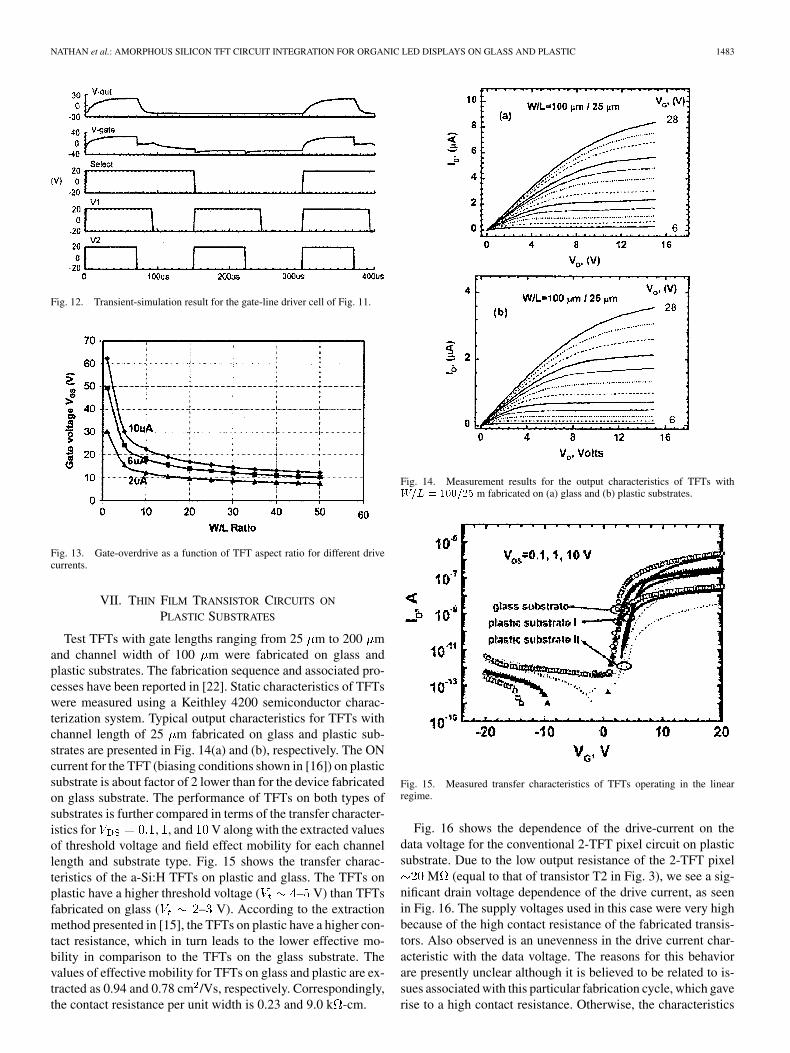
Fig. 12. Transient-simulation result for the gate-line driver cell of Fig. 11.
Fig. 13. Gate-overdrive as a function of TFT aspect ratio for different drivecurrents.
VII. THIN FILM TRANSISTOR CIRCUITS ON
PLASTIC SUBSTRATES
Test TFTs with gate lengths ranging from 25 m to 200 mand channel width of 100 m were fabricated on glass andplastic substrates. The fabrication sequence and associated pro-cesses have been reported in [22]. Static characteristics of TFTswere measured using a Keithley 4200 semiconductor charac-terization system. Typical output characteristics for TFTs withchannel length of 25 m fabricated on glass and plastic sub-strates are presented in Fig. 14(a) and (b), respectively. The ONcurrent for the TFT (biasing conditions shown in [16]) on plasticsubstrate is about factor of 2 lower than for the device fabricatedon glass substrate. The performance of TFTs on both types ofsubstrates is further compared in terms of the transfer character-istics for , , and V along with the extracted valuesof threshold voltage and field effect mobility for each channellength and substrate type. Fig. 15 shows the transfer charac-teristics of the a-Si:H TFTs on plastic and glass. The TFTs onplastic have a higher threshold voltage ( – V) than TFTsfabricated on glass ( – V). According to the extractionmethod presented in [15], the TFTs on plastic have a higher con-tact resistance, which in turn leads to the lower effective mo-bility in comparison to the TFTs on the glass substrate. Thevalues of effective mobility for TFTs on glass and plastic are ex-tracted as 0.94 and 0.78 cm /Vs, respectively. Correspondingly,the contact resistance per unit width is 0.23 and 9.0 k -cm.
Fig. 14. Measurement results for the output characteristics of TFTs withW=L = 100=25 m fabricated on (a) glass and (b) plastic substrates.
Fig. 15. Measured transfer characteristics of TFTs operating in the linearregime.
Fig. 16 shows the dependence of the drive-current on thedata voltage for the conventional 2-TFT pixel circuit on plasticsubstrate. Due to the low output resistance of the 2-TFT pixel
M (equal to that of transistor T2 in Fig. 3), we see a sig-nificant drain voltage dependence of the drive current, as seenin Fig. 16. The supply voltages used in this case were very highbecause of the high contact resistance of the fabricated transis-tors. Also observed is an unevenness in the drive current char-acteristic with the data voltage. The reasons for this behaviorare presently unclear although it is believed to be related to is-sues associated with this particular fabrication cycle, which gaverise to a high contact resistance. Otherwise, the characteristics

1484 IEEE JOURNAL OF SOLID-STATE CIRCUITS, VOL. 39, NO. 9, SEPTEMBER 2004
Fig. 16. Photomicrograph of the conventional 2-TFT pixel circuit on plastic substrate and its measured drive current characteristics for different supply voltage.
Fig. 17. Photomicrograph of the 4-TFT pixel circuit on plastic substrate and its measured drive current characteristics for different supply voltage.
are expected to be linear for a reasonably large range of datavoltage. The saturation of the drive current at large is dueto the transistor T2 moving from saturation to linear regime ofoperation.
Fig. 17 shows the drive-current characteristics of the cur-rent-programmed 4-TFT circuit on the plastic substrate. The cir-cuit can provide a constant drive current through the OLED ir-respective of changes in and of the drive TFT in Fig. 4.Besides the improved stability, the 4-T circuit has a distinct per-formance advantage over the 2-T circuit in terms of its higheroutput resistance, which reduces the dependence of the drivecurrent on drain voltage (see Fig. 17). The current stability in thepresence of shift for the 2-T and 4-T circuits on a plastic sub-strate is very similar to that described earlier in Fig. 7. Here, weagain observed that while the drive current supplied by the 2-T
circuit drops by over 50%, the current supplied by the 4-T circuitremains essentially constant. The initial drop in current over thefirst hour of operation can be viewed as the burn-in phase, and isa characteristic of a-Si:H pixel circuits on both glass and plastic.Fig. 18 illustrates a cascode current mirror on plastic substrate.Its superiority over other current source circuits is evident fromits high output resistance, which has significantly reduced thedrive current dependence on the drain voltage of T3 (see Fig. 9),and the highly linear response.
VIII. CONCLUSION
In this paper, 4-TFT -shift-resistant current drivenAMOLED pixel has been presented. Equivalent - circuitmodels for both voltage and current programmed pixel circuits

NATHAN et al.: AMORPHOUS SILICON TFT CIRCUIT INTEGRATION FOR ORGANIC LED DISPLAYS ON GLASS AND PLASTIC 1485
Fig. 18. Photomicrograph of the cascade current mirror circuit on plastic substrate and its measured drive current characteristics for different supply voltage.
were developed and based on this, the feasibility of a QVGAarray for 60-Hz video-quality frame-rate was discussed alongwith an optimal biasing strategy for management andits effect on drive current. Finally, we successfully demon-strated the integration of a-Si:H TFT circuits on plastic forAMOLED applications. Despite the high contact resistance and
metastability of the TFTs, the circuits were able to providestable and predictable drive currents.
REFERENCES
[1] T. Tsukada, “Active-matrix liquid-crystal displays,” in Technologyand Applications of Hydrogenated Amorphous Silicon, R. A. Street,Ed. New York: Springer, 2000, pp. 7–93.
[2] R. M. A. Dawson and M. G. Kane, “Pursuit of active matrix organic lightemitting diode displays,” in Dig. Tech. Papers, SID Int. Symp., San Jose,CA, June 2001, pp. 372–375.
[3] A. Nathan, D. Stryakhilev, P. Servati, K. Sakariya, A. Kumar, K. S.Karim, and A. Sazanov, “Low temperature a-Si:H pixel circuits for me-chanically flexible AMOLD displays at 120 C for OLED-TFT arrayson plastic substrates,” in Mat. Res. Soc. Symp. Proc., vol. 769, 2003, pp.29–34.
[4] Welcome to 2010 [Online]. Available: http://www.businessweek.com/reprints/00-10/b3 671 021.htm
[5] Cambridge Display Technology. [Online]. Available: http://www.cdtltd.co.uk/
[6] Universal Display Corp. [Online]. Available: http://www.universaldis-play.com/
[7] K. Sakariya, P. Servati, D. Stryahilev, and A. Nathan, “V -shift compen-sated a-Si:H pixel circuits for AMOLED displays,” in Proc. Eur. Display2002: 22nd Int. Display Research Conf., Nice, France, Oct. 2002, pp.609–612.
[8] P. Servati, S. Prakash, A. Nathan, and C. Py, “Amorphous silicon drivercircuits for OLED displays,” J. Vac. Sci. Technol. A, vol. 20, no. 4, pp.1374–1378, 2002.
[9] D. P. Gosain, A. Machida, T. Fujino, Y. Hitsuda, K. Nakano, and J. Sato,“Formation of (100)-textured Si film using an excimer laser on glasssubstrate,” Jpn. J. Appl. Phys., vol. 42, pp. L135–L137, 2003.
[10] P. Servati, K. S. Karim, and A. Nathan, “Static characteristics of a-Si:Hdual-gate TFTs,” IEEE Trans. Electron Devices, vol. 50, pp. 926–932,2003.
[11] P. Servati and A. Nathan, “Modeling of the reverse characteristics ofa-Si:H TFTs,” IEEE Trans. Electron Devices, vol. 49, pp. 812–819, May2002.
[12] , “Modeling of the static and dynamic behavior of a-Si:H TFTs,” J.Vac. Sci. Technol. A, vol. 20, no. 4, pp. 1374–1378, 2002.
[13] M. J. Powell, C. van Berkel, I. D. French, and D. H. Nicholls, “Biasdependence of instability mechanisms in amorphous silicon thin filmtransistors,” Appl. Phys. Lett., vol. 51, p. 1242, 1987.
[14] K. S. Karim, A. Nathan, and J. A. Rowlands, “Amorphous silicon pixelamplifier with�V compensation for low noise digital fluoroscopy,” inIEEE IEDM Tech. Dig., San Francisco, CA, Dec. 2002, pp. 215–218.
[15] P. Servati, D. Striakhilev, and A. Nathan, “Above-threshold parameterextraction and modeling for amorphous silicon thin-film transistors,”IEEE Trans. Electron Devices, vol. 50, pp. 2227–2235, 2003.
[16] G. Gu and S. R. Forrest, “Design of flat-panel displays based on organiclight-emitting devices,” IEEE J. Select. Topics Quantum Electron., vol.4, pp. 83–99, 1998.
[17] Vitex Systems [Online]. Available: http://www.vitexsys.com/solu-tion.html
[18] Y. He, R. Hattori, and J. Kanicki, “Current-source a-Si:H thin film tran-sistor circuit for active matrix organic light emitting displays,” IEEEElectron Device Lett., vol. 21, pp. 590–592, 2000.
[19] M. J. Powell, C. van Berkel, and J. R. Hughes, “Time and temperaturedependence of instability mechanisms in amorphous silicon thin filmtransistors,” Appl. Phys. Lett., vol. 54, no. 14, p. 1323, 1989.
[20] W. B. Jackson and M. D. Moyer, “Creation of near interface defectsin hydrogenated amorphous silicon-silicon nitride heterojunctions: Therole of hydrogen,” Phys. Rev. B, vol. 36, p. 6217, 1989.
[21] E. Elmore, “The transient response of damped linear networks with par-ticular regard to wideband amplifiers,” J. Appl. Phys., vol. 19, pp. 55–63,Jan. 1948.
[22] D. Stryakhilev, A. Sazonov, and A. Nathan, “Amorphous silicon nitridedeposited at 120 C for OLED-TFT arrays on plastic substrates,” J. Vac.Sci. Technol. A, vol. 20, no. 4, pp. 1087–1090, 2002.
Arokia Nathan (S’84–M’88–SM’99) received thePh.D. degree in electrical engineering from theUniversity of Alberta, Edmonton, Alberta, Canada,in 1988, where he was engaged in research relatedto the physics and numerical modeling of semicon-ductor microsensors.
In 1987, he joined LSI Logic Corporation, SantaClara, CA, where he worked on advanced mul-tichip packaging techniques and related issues.Subsequently, he was at the Institute of QuantumElectronics, ETH Zürich, Switzerland. In 1989, he
joined the Department of Electrical and Computer Engineering, University ofWaterloo, Canada, where he is currently a Professor. In 1995, he was a VisitingProfessor at the Physical Electronics Laboratory, ETH Zürich. His presentresearch interests lie in fabrication of devices, circuits, and systems using dis-ordered semiconductor, including organic, materials on rigid and mechanicallyflexible substrates for large area electronics. He held the DALSA/NSERCindustrial research chair in sensor technology, and is a recipient of the NaturalSciences and Engineering Research Council E. W. R. Steacie Fellowship. Hecurrently holds the Canada Research Chair in Nanoscale Elastic Circuits. Hehas published extensively in the field of sensor technology and CAD, and thinfilm transistor electronics, and is a coauthor of the book Microtransducer CAD(Springer, 1999).

1486 IEEE JOURNAL OF SOLID-STATE CIRCUITS, VOL. 39, NO. 9, SEPTEMBER 2004
Anil Kumar received the Bachelors degree in elec-tronics engineering in May 1998 from the Institute ofTechnology BHU, India. In January 2001, he joinedthe University of Waterloo, Canada, as a Mastersstudent in electrical and computer engineering.Currently, he is working toward the Ph.D. degree inthe field of AMOLED display.
From 1998 to 2000, he was with Motorola Semi-conductors as a Circuit Design Engineer and workedon SRAMs/IOs/VCOs.
Mr. Kumar is the current recipient of the CITO Stu-dent Research Excellence Scholarship, 2003.
Kapil Sakariya received the B.Sc. degree in elec-trical engineering from the University of Manitoba,Canada, in 2001, and the M.A.Sc. degree from theUniversity of Waterloo, Canada, in 2002. He is cur-rently working toward the Ph.D. degree at the Uni-versity of Waterloo.
His research interests are in the field of active ma-trix OLED display design using amorphous silicontechnology.
Mr. Sakariya has received numerous provincialand national scholarships including two Natural
Sciences and Engineering Research Council of Canada (NSERC) awards.
Peyman Servati (S’00) received the B.Sc. degree(with honors) in electronics engineering from theUniversity of Tehran in 1998, and the M.A.Sc. andPh.D. degrees from the University of Waterloo,Waterloo, Ontario, Canada, in 2000 and 2004,respectively. His dissertation was on mechanicallyflexible TFTs and circuits for active matrix organiclight-emitting diode (AMOLED) displays andother large area applications. As an undergraduatestudent, he was involved in device simulations in thethin-film laboratories at the University of Tehran.
Subsequently, he joined the a-SiDIC group of the University of Waterloo.He is currently with IGNIS Innovation, Inc., a spin-off company from the
University of Waterloo, working on stable TFT backplanes for AMOLED dis-plays. His present research interest lies in disordered organic and silicon TFTsfor displays and bio applications.
Mr. Servati was a recipient of the Bronze Medal in the XXV I.Ph.O. competi-tions held in Beijing, China, 1994, and currently holds the Natural Sciences andEngineering Research Council (NSERC) of Canada Postgraduate Scholarship.
Sanjiv Sambandan (S’02) received the B.Tech. de-gree (with honors) in electrical engineering from theIndian Institute of Technology, Kharagpur, in 2002.His dissertation was on the development of an opticfiber based cryogenic temperature sensor, for whichhe received the Institute Proficiency Prize 2002. Hereceived the M.A.Sc. degree in electrical and com-puter engineering in 2003 at the University of Wa-terloo, Ontario, Canada, for his thesis on a-Si:H TFT-based driver circuits for AMOLED displays. He iscurrently working toward the Ph.D. degree at the Uni-
versity of Waterloo.
Denis Striakhilev (M’03) received Dipl.Eng. degree(technology of microelectronics) and Ph.D. degree insemiconductor physics from the Moscow Institute ofElectronic Technology (Technical University), MIET(TU) Moscow, Russian Federation, in 1991 and 1996,respectively. During his Ph.D. work, he studied struc-tural, electrical and optical properties of amorphoussemiconductor alloys for photovoltaic applications.
During 1997–1998, he was a Visiting Scientistat the Department of Physics, University of Kaiser-slautern, Kaiserlautern, Germany, and a holder of
a DAAD research scholarship. Subsequently, he was a Research Fellow atthe Department of Material Science, MIET(TU) and Assistant Professor atthe Department of Physics, Yaroslavl State Pedagogical University, Yaroslavl,Russia. Since 2000, he has been with the Department of Electrical andComputer Engineering, University of Waterloo, Waterloo, Ontario, Canada.His present research is primarily related to thin-film devices for display andimaging applications including mechanically flexible electronic devices. He isauthor or coauthor of more than 30 publications and two patents.
Dr. Striakhilev is a member of the Materials Research Society, and Societyfor Information Displays.